31295018467604.pdf - ttu dspace home
TRANSCRIPT
DESIGN AND IMPLEMENTATION OF A POWER
CONVERTER FOR SOIL VITRIFICATION APPLICATION
by
ROBERTO CARLOS IZQUIERDO GARCIA, B.S.E.
A THESIS
IN
ELECTRICAL ENGINEERING
Submitted to the Graduate Faculty of Texas Tech University in
Partial Fulfillment of the Requirements for
the Degree of
MASTER OF SCIENCE
IN
ELECTRICAL ENGINEERING
Approved
August, 2001

ACKNOWLEDGMENT
Thanks to God for make my what I am.
Thanks to my family for their love, support and patience. To my parents who
encourage me to go further, to prepare my self better. Thank to my brother and sister for
encouraging me.
I want to thank Dr. Ramirez from UDLAP and Dr. Hagler from TTU for their
support and help to participate in the dual program between TTU and UDLAP. Thanks to
all the professors in the UDLAP who provide me with the tools to succeed in TTU.
I also want to thank Dr Dickens for his help and for the opportunity to learn from
him, for him support and guidence.
Thanks to all my friends in Lubbock. You help me to grown as a person and help
me to go through difficult situations.
Most of all, I want to thanks to a person who give me her love, support, patience
and most of all, the strength to complete one of my most difficult challenges. She has
been my reason to keep going.
Te amo, Edna Karina.
11
TABLE OF CONTENT
ACKNOWLEDGMENTS ii
ABSTRACT v
LIST OF TABLE vi
LIST OF FIGURES vii
CHAPTER
1. INTRODUCTION 1
2. SOIL STABILIZER 2
2.1 Overview 2
3. BUCK CONVERTER 3
3.1 Dc-dc converter 3
3.2 Buck converter 5
3.3 Continuous conduction mode 6
3.4 Discontinuous conduction mode 8
4. SIMULATION 11
4.1 Buck converter 11
4.2 Controller 13
4.2.1 Voltage mode configuration 14
4.2.2 Current mode configuration 18
5. IMPLEMENTATION 26
5.1 Electric diagram 26
5.1.1 Components 26
5.2 Microcontroller 68HC12 28
5.2.1 PWM module 28
5.2.2 Analog to Digital converter 32
5.2.3 Keyboard 33
5.2.4 LCD 36
5.3 First implemented design 38
5.3.1 Interface Boards 40
iii

5.3.2 Control approach
5.3.2.1 Increment-decrement..
5.3.2.2 Proportional control...
5.4.1 Board
5.4.2 Control annroach
5.4.3 Software
6. CONCLUSIONS
BIBLIOGRAPHY
APPENDIX
A.
B.
C
D.
68HC12CODE
PSPICE SIMULATION
CONTROLLER BOARDS
TORCH TRUCK
42
42
46
49
51
54
56
60
61
62
65
68
79
IV

ABSTRACT
Texas Tech in conjunction with Montech Research proposed the constmction of a
soil stabilizer using a power graphite torch capable of generating hot plasma gas to melt
the soil. The project will be used by the Texas Department of Transportation (TDOx).
The present work is a description of the electrical modules implemented to control
the power of the equipment. The use of a buck converter to control the output power is
proposed. Texas Tech was in charge of the constmction of the electrical part of the
project, a power supply capable to control lOOkW.
The TDOx proposed the project because for some applications a material stronger
than concrete is required, and the melted soil is three times stronger than concrete.
The results observed on the field shows that it is possible to melt down the soil
with an output of SOkW. With further improvement on the design of the power modules it
is possible to control up to lOOkW.

LIST OF TABLES
4.1 Simulation cases 21
5.1 Input keyboard for the matrix board 35
5.2 LCD Instmction set 38
5.3 68HC12 ports 52
5.4 Multiplexer outputs 54
5.5 Keys function 58
VI
LIST OF FIGURES
2.1 Soil stabilizer overview 2
3.1 Switch mode dc-dc conversion 3
3.2 Pulse width modulator: (a) block diagram; (b) comparator signals... 4
3.3 Step-down dc-dc converter 5
3.4 Step-down converter states: (a) switch on: (b) switch off 6
3.5 Continuous conduction mode 6
3.6 Boundary between the continuous and discontinuous mode 8
3.7 Discontinuous conduction in step-down converter 8
3.8 Output voltage ripple in a step-down converter 10
4.1 Buck converter model for PSpice 11
4.2 Simulation ofthe model at D = 50% 12
4.3 Discontinuous conduction mode 13
4.4 Voltage control mode 14
4.5 Voltage controller mode 14
4.6 Plasma burner 15
4.7 Current control with one module 15
4.8 Error signal 16
4.9 Current control with three modules: Iset = 200A 17
4.10 Current control with different setpoints 17
4.11 Current control: (a) Controller, (b) PWM waveform 18
4.12 Use ofthe flip-flop as the controller 19
4.13 PWM control signals: (a) start, (b) reset and (c) clock signal 19
4.14 Current mode 20
4.15 Setpointof200A 20
4.16 Equal setpoints and inductances 21
4.17 Different setpoints, equal inductances 22
4.18 Low load inductance 22
4.19 Different setpoint, low load inductance 23
Vll

4.20 Same setpoints, different inductances 23
4.21 Same setpoint, different inductances 24
4.22 Equal inductances, same setpoint 24
4.23 Equal inductances, same setpoint, low load inductance 25
5.1 Electric diagram 26
5.2 Rectifier bridge (a) symbolic and (b) internal diagram 27
5.3 IGBTSkiiP 1442. Buck converter 27
5.4 Left-aligned waveform, positive polarity 29
5.5 PWM clock chains 30
5.6 PWM left-aligned output channel 31
5.7 Analog-to-Digital Converter 32
5.8 4 x 4 Matrix keyboard 33
5.9 Schematic keyboard connections 34
5.10 LCD Connections 37
5.11 Address lines on the LCD 37
5.12 Block diagram 39
5.13 First design of electrical diagram 39
5.14 Interface board with the HC12 40
5.15 Configuration for the optocouplers 40
5.16 Lowpass filter 41
5.17 Filter design using Simplorer: (a) model; (b) simulation 42
5.18 Increment-decrement 43
5.19 Buck converter on Simplorer 44
5.20 Control stages on Simplorer 44
5.21 Simulation with no initial current on the inductance 45
5.22 Initial condition, IL = 400A 46
5.23 Feedback diagram 46
5.24 Sampling model 47
5.25 Current and Duty cycle 48
5.26 Second design: (a) Main circuit; (b) interior ofthe module 50
Vlll

5.27 Second interface 51
5.28 Internal diagram ofthe controller board 52
5.29 Controller module interface 53
5.30 New PWM controller 55
5.31 Second configuration 55
5.32 Software diagram 56
5.33 Display shell 57
5.34 Registers relations 58
5.35 Display view: (a) Power mode and (b) Current mode 58
B. 1 Plasma burner 66
B.2 Current mode controller 67
C I 68HC12 interface with the IGBTs 69
C.2 Pcboard silk side of diagram on Figure C I 70
C.3 Pcboard component side of diagram on Figure C I 70
C.4 Pcboard solder side of diagram on Figure C I 70
C.5 Schematic ofthe analogic digital interface 71
C.6 Pcboard silk side of diagram on Figure C.5 72
C.7 Pcboard component side of diagram on Figure C.5 72
C8 Pcboard solder side of diagram on Figure C5 72
C.9 Controller box interface between the HC12 and the keyboard-LCD. 73
CIO Pcboard silk side of diagram on Figure C.9 74
C11 Pcboard component side of diagram on Figure C.9 74
C12 Pcboard solder side of diagram on Figure C.9 74
C.13 PWM controller schematic 75
C.14 Pcboard silk side of diagram on Figure C.13 76
C.15 Pcboard component side of diagram on Figure C.13 76
C16 Pcboard solder side of diagram on Figure C.13 76
C.17 Controller interface 77
C.18 Analog interface 77
C.19 68HC12 General interface 78
IX

C.20 Box cover 78
D. 1 Mechanical system 80
D .2 Transformer 80
D.3 Power converter operation 81

CHAPTER 1
INTRODUCTION
A relatively new branch of electronics is power electronics, where the control of
hundred of volts and amperes is achieved with new semiconductor devices such as power
diodes, BJT, Power MOSFETS, thyristors and Insulated Gate Bipolar Transistors (IGBT)
[1]. Such devices allow us to achieve a better performance on diverse applications and
also allow new control techniques based on this technology. One branch is related to the
design of power supplies.
A power supply is a device capable of maintaining a constant voltage or current
delivered to a load using diverse techniques. Among the power supplies, there are the dc-
dc topologies, which have a constant voltage over a period of time. The control ofthe
output power becomes a problem when the load demands high power from the input, then
risking the integrity ofthe application. Therefore it is important to have an adequate
control over the load power to ensure the integrity ofthe application.
To convert and control the voltage we have different topologies. Among them
there is one topology known as the Buck Converter, also know as a Step Down
Converter. The buck converter is a good option to control a dc-dc voltage, because it
simple and efficient. The buck converter is a voltage controller whose voltage output is
lesser than or equal to the input voltage.
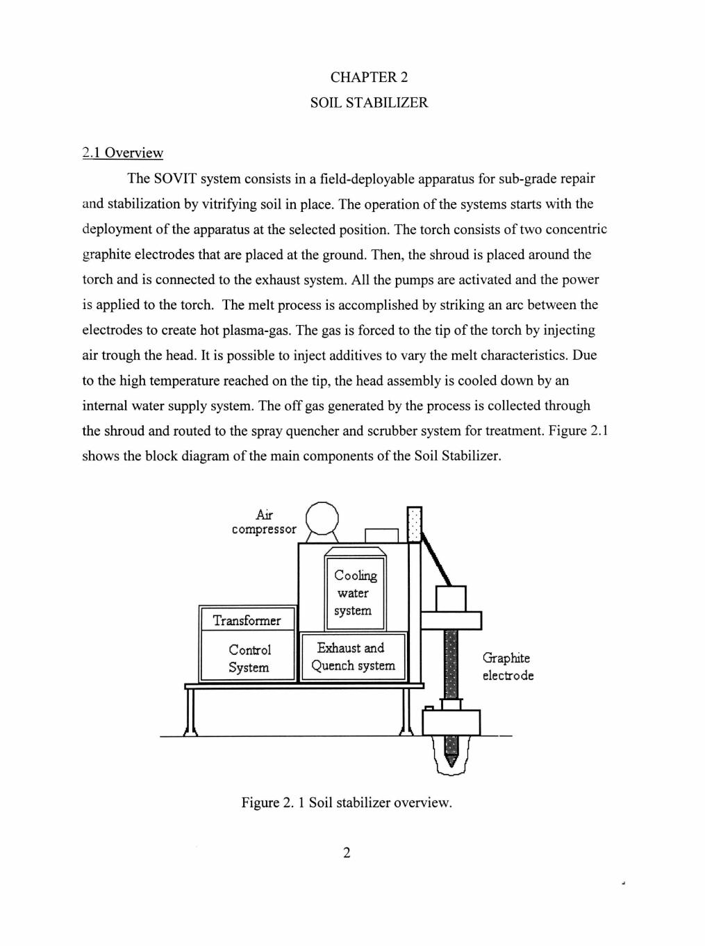
CHAPTER 2
SOIL STABILIZER
2.1 Overview
The SOVIT system consists in a field-deployable apparatus for sub-grade repair
and stabilization by vitrifying soil in place. The operation ofthe systems starts with the
deployment ofthe apparatus at the selected position. The torch consists of two concentric
graphite electrodes that are placed at the ground. Then, the shroud is placed around the
torch and is connected to the exhaust system. All the pumps are activated and the power
is applied to the torch. The melt process is accomplished by striking an arc between the
electrodes to create hot plasma-gas. The gas is forced to the tip ofthe torch by injecting
air trough the head. It is possible to inject additives to vary the melt characteristics. Due
to the high temperature reached on the tip, the head assembly is cooled down by an
internal water supply system. The off gas generated by the process is collected through
the shroud and routed to the spray quencher and scrubber system for treatment. Figure 2.1
shows the block diagram ofthe main components ofthe Soil Stabilizer.
A\
Air compressor
Transformer
Control System
Exhaust and Quench system Graphite
electrode
Figure 2. 1 Soil stabilizer overview.
CHAPTER 3
BUCK CONVERTER
3.1 Dc-dc Converter
Nowadays, the dc-dc is widely used in regulated power supplies and in dc motors
drives. In most applications, the voltage input of these converters comes from non-
regulated dc sources. Switch mode dc-dc converters are used to control the output
voltage, converting them from unregulated to regulated dc input at a desired voltage
level. Some dc-dc converters are:
a. Step-down (buck) converter,
b. Step-up (boost) converter,
c. Step-down/step-up converter,
d. Cuk converter.
The first two converters are basic configurations while the third and fourth are a
combination ofthe first two.
On dc-dc converters, the average output voltage must be controlled to obtain a
desired level, even if the input voltage fluctuates. A switch mode dc-dc converter uses
one or more switches to convert a dc level to another. In a dc-dc converter with a defined
input voltage, the average output voltage is controlled by controlling the switch on and
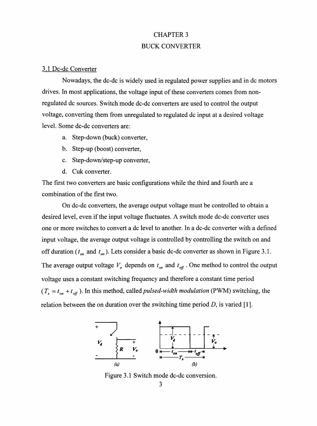
off duration (t^„ and t^^). Lets consider a basic dc-dc converter as shown in Figure 3.1.
The average output voltage V^ depends on r „ and / ^ . One method to control the output
voltage uses a constant switching frequency and therefore a constant time period
(7 ^ = t^^ + t.j.). In this method, called pulsed-width modulation (PWM) switching, the
relation between the on duration over the switching time period D, is varied [1].
^
K + R Vo
(a)
I 1.
O M ^on W^V""
(b)
Figure 3.1 Switch mode dc-dc conversion. 3
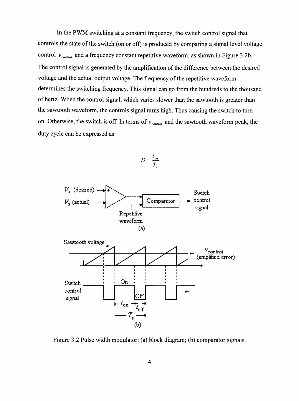
In the PWM switching at a constant frequency, the switch control signal that
controls the state ofthe switch (on or off) is produced by comparing a signal level voltage
control v ,„ / and a frequency constant repetitive waveform, as shown in Figure 3.2b.
The control signal is generated by the amplification ofthe difference between the desired
voltage and the actual output voltage. The frequency ofthe repetitive waveform
determines the switching frequency. This signal can go from the hundreds to the thousand
of hertz. When the control signal, which varies slower than the sawtooth is greater than
the sawtooth waveform, the controls signal turns high. Thus causing the switch to tum
on. Otherwise, the switch is off. In terms of v^^^,^^, and the sawtooth waveform peak, the
duty cycle can be expressed as
D = T.
V^ (desired)
VQ (actual)
Sawtooth voltage
Repetitive waveform
(a)
Switch control signal
(b)
Switch > control
signal
^control (amplified error)
Figure 3.2 Pulse width modulator: (a) block diagram; (b) comparator signals.
3.2 Step-down (Buck) converter
A step-down converter produces a lower average output voltage than the dc input
voltage. Its main application is in regulated dc power supply and dc motor speed control
[1]. Based on the diagram of Figure 3.1a, the basic operation ofthe step-down converter
can be explained. Assuming an ideal switch and a purely resistive load, the instantaneous
output voltage will be as shown on Figure 3.1b, where the output voltage depends on the
switch position. The average output voltage can be calculated in terms ofthe switch duty
ratio:
A' 0 T.
L. \ 1 1 I '"" 1 1 1 V, =- lv,it)dt = - jV,dt+ \Odt =-\ V, \dt ^V,=DV,.
0 J
By varying the duty ratio t^^ IT, ofthe switch, V^ can be controlled. The circuit
of Figure 3.1a has two inconvenient on real applications, (1) the load will be inductive,
and (2) the output voltage fluctuates between 0 and V^, something not possible on some
applications. Even with a resistive load, we can assume to have an inductance associated
with the circuit. This energy would have to be absorbed (or dissipated) by the switch, and
therefore it can be destroyed.
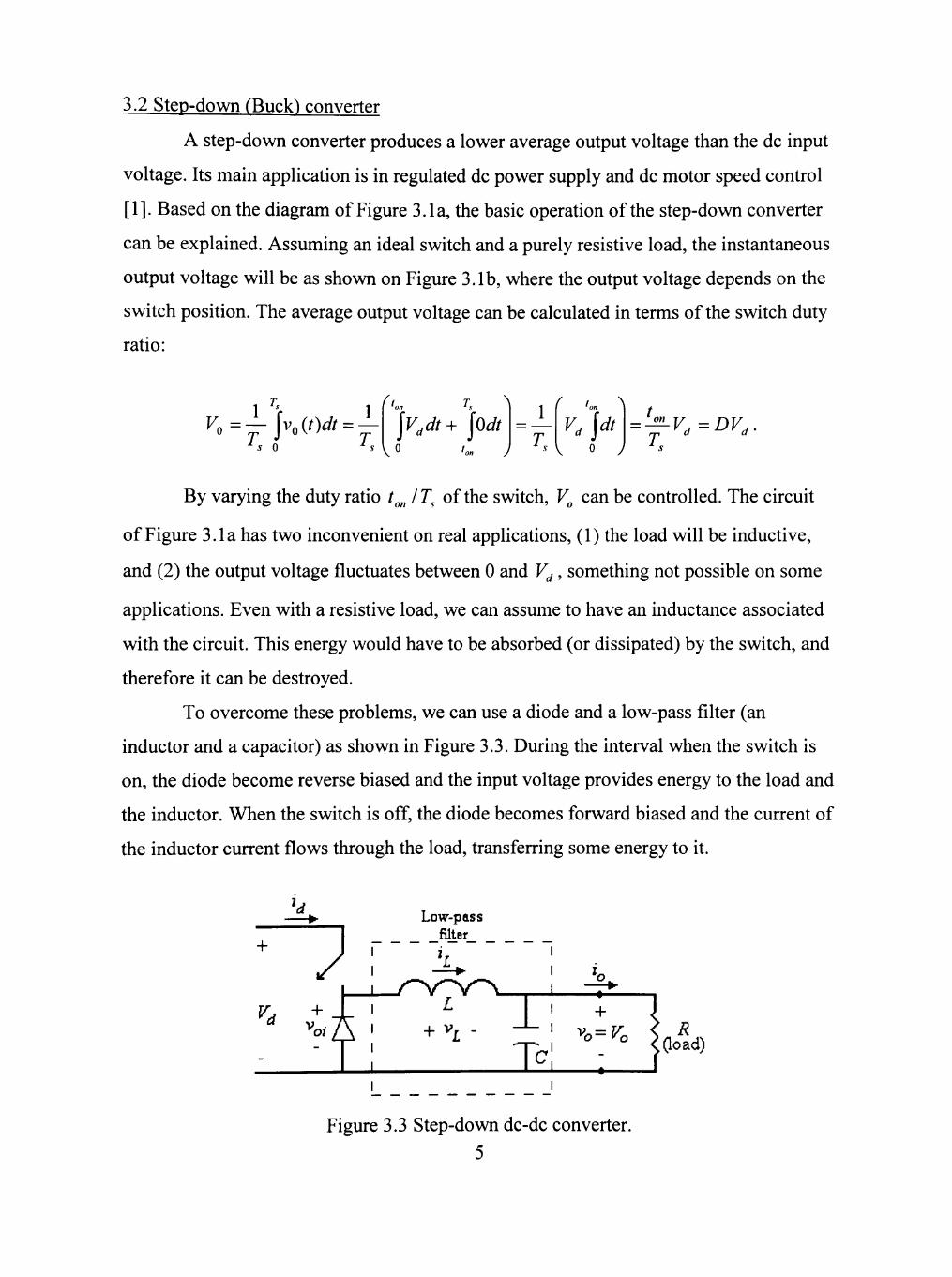
To overcome these problems, we can use a diode and a low-pass filter (an
inductor and a capacitor) as shown in Figure 3.3. During the interval when the switch is
on, the diode become reverse biased and the input voltage provides energy to the load and
the inductor. When the switch is off, the diode becomes forward biased and the current of
the inductor current flows through the load, transferring some energy to it.
Low-pass ater
Figure 3.3 Step-down dc-dc converter.
5
The capacitor in the filter has to be large for applications where the instantaneous
voltage at the output needs to be almost constant, v^=V^. From Figure 3.3, we can
observe that the average inductor current / is equal to the average output current /^
since the average capacitor current in steady state is zero [1].
3.3 Continuous conduction mode
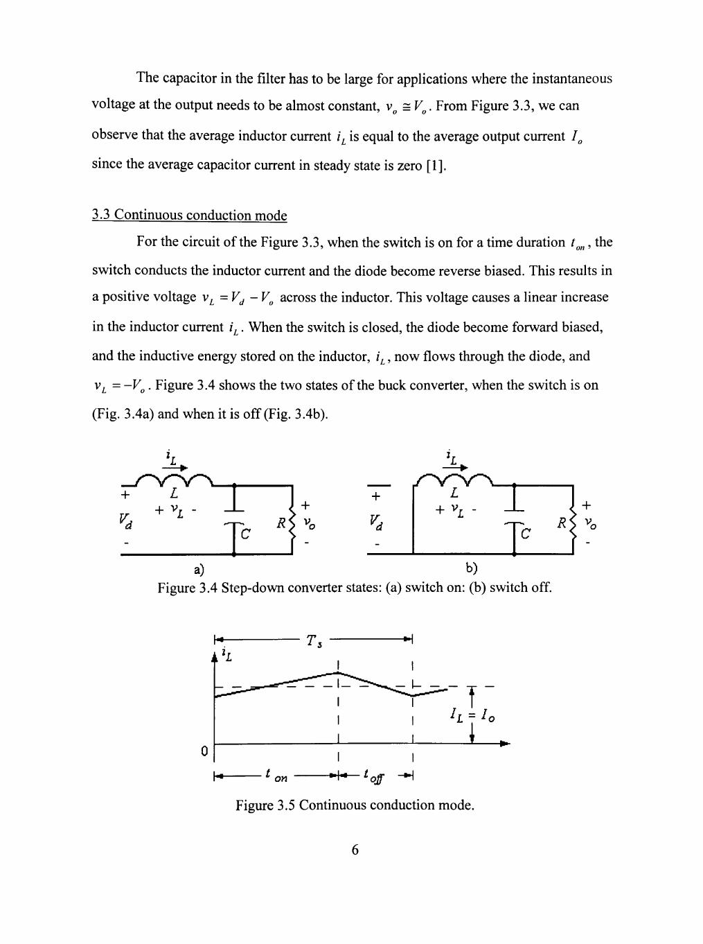
For the circuit ofthe Figure 3.3, when the switch is on for a time duration /^„, the
switch conducts the inductor current and the diode become reverse biased. This results in
a positive voltage v^=Vj - V^ across the inductor. This voltage causes a linear increase
in the inductor current /^. When the switch is closed, the diode become forward biased,
and the inductive energy stored on the inductor, z , now flows through the diode, and
v^ = -V^. Figure 3.4 shows the two states ofthe buck converter, when the switch is on
(Fig. 3.4a) and when it is off (Fig. 3.4b).
^0 +
R
a) b) Figure 3.4 Step-down converter states: (a) switch on: (b) switch off.
Figure 3.5 Continuous conduction mode.

The integral ofthe inductor voltage over a period of time must be zero.
['v,dt=l""v,dt+f'v,dt = 0
Therefore:
{y,-K>o.=K{T,-0
V t -V t =VT -V t d on o on o s o on
K'o« = vj.
or
V t o on r \
In this mode, the output voltage varies linearly with the duty cycle ofthe switch.
Neglecting power losses associated to the circuit, the input power P^ equals the output
power P^:
P = P '^d ^o
VJ,=VJ,
In continuous conduction mode, the step-down converter behaves as a transformer
where the turns ratio ofthe equivalent transformer can be controlled electronically in a
range from 0 to 1 by controlling the duty cycle. When the current ofthe inductor goes to
zero at the end ofthe / ^ period, as shown in Figure 3.6, the converter is at the boundary
ofthe continuous mode. At this boundary, the average inductor current, where the
subscript B refers to the boundary, is
^ LB rs^L,peak "J T ^ '^ °' 97" ^ a ) ~ ^ oB

on 'off - ^ K
Figure 3.6 Boundar}' between the continuous and discontinuous mode.
Therefore, if the average output current becomes less than /^^. then z becomes
discontinuous.
3.4 Discontinuous conduction mode
In this mode, either the input voltage V^ or the output voltage V^ remains
constant during the operation. Figure 3.7 shows the discontinuous mode for both cases.
Onl}' the case with constant input voltage will be discussed.
^ i
^L,peak
> ^ ^
..^^^ Vd-Vo k
\^I
t Vo
y r
^ ^ 1
^2 Ts
A Ir = L
•DT, >^^—AjTi »' »| K-
Figure 3.7 Discontinuous conduction in step-down converter.
In applications were the input voltage V^ is constant, the output voltage V^ is
controlled by adjusting the value of D. From last equation and because V^ = DV^, the
average inductor current at the edge ofthe continuous-conduction mode is
TV
2L
8

The maximum output current that is required to be on the boundary ofthe
continuous mode is found at D=0.5 (assuming that we maintain constant the parameters
values). At D=0.5, the maximum output current required is
T V LB,max Q J
The voltage ratio can be calculated in the discontinuous mode. Lets assume that
the converter is operating at the boundary ofthe continuous mode, as in Figure 3.6, for
given values of T, L, V^. If these parameters are left constant and the output load power
decreases (i.e. the load resistance goes up), then the average inductor current will
decrease, and therefore the output voltage will increase, as shown in Figure 3.7. This
results in a discontinuous inductor current. During the interval IsiTs where the inductor
current is zero, the power to the load resistance is supplied by the filter capacitor. The
inductor voltage at this interval is zero.
3.5 Output voltage ripple
For the previous analysis, the output capacitor is assumed to be large enough as to
achieve v (J) = V^. With a continuous conduction mode as Figure 3.8 shows, the output
volt ripple can be calculated. The peak to peak voltage ripple can be written as
AV = ''^^^^ CI 1 1
where
A/,=^(i-z))r,
By substituting A/ on AF„ gives
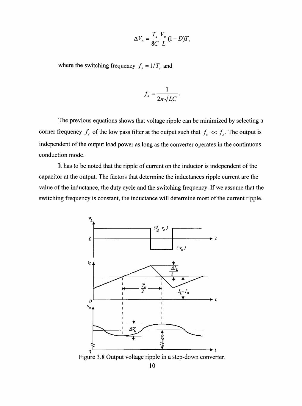
T V AV^=-A-^(l-D)T^
" SC L
where the switching frequency f =\/T^ and
/ . = iTlyflC
The previous equations shows that voltage ripple can be minimized by selecting a
comer frequency / , ofthe low pass filter at the output such that / , « /^. The output is
independent ofthe output load power as long as the converter operates in the continuous
conduction mode.
It has to be noted that the ripple of current on the inductor is independent ofthe
capacitor at the output. The factors that determine the inductances ripple current are the
value ofthe inductance, the duty cycle and the switching frequency. If we assume that the
switching frequency is constant, the inductance will determine most ofthe current ripple.
(V,-v )
(-^n)
-> t
* • t
Figure 3.8 Output voltage ripple in a step-down converter. 10
CHAPTER 4
SIMULATION
The present chapter will present simulations of a buck converter and for the
control to be implemented on the power converter. The details ofthe power converter
will be explained on chapter 5. The models presented here are based on libraries from the
comse Power Electronics imparted by Dr Michel Giesselman
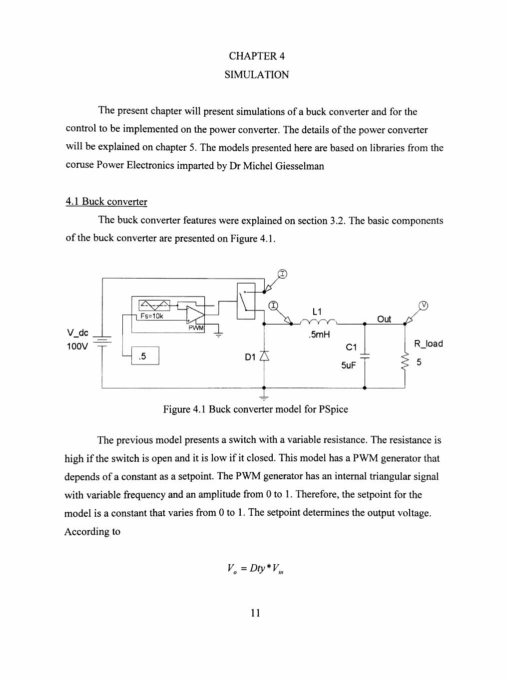
4.1 Buck converter
The buck converter features were explained on section 3.2. The basic components
ofthe buck converter are presented on Figure 4.1.
V dc
100V - r
Figure 4.1 Buck converter model for PSpice
The previous model presents a switch with a variable resistance. The resistance is
high if the switch is open and it is low if it closed. This model has a PWM generator that
depends of a constant as a setpoint. The PWM generator has an internal triangular signal
with variable frequency and an amplitude from 0 to 1. Therefore, the setpoint for the
model is a constant that varies from 0 to 1. The setpoint determines the output voltage.
According to
K=Dty*v,„
11
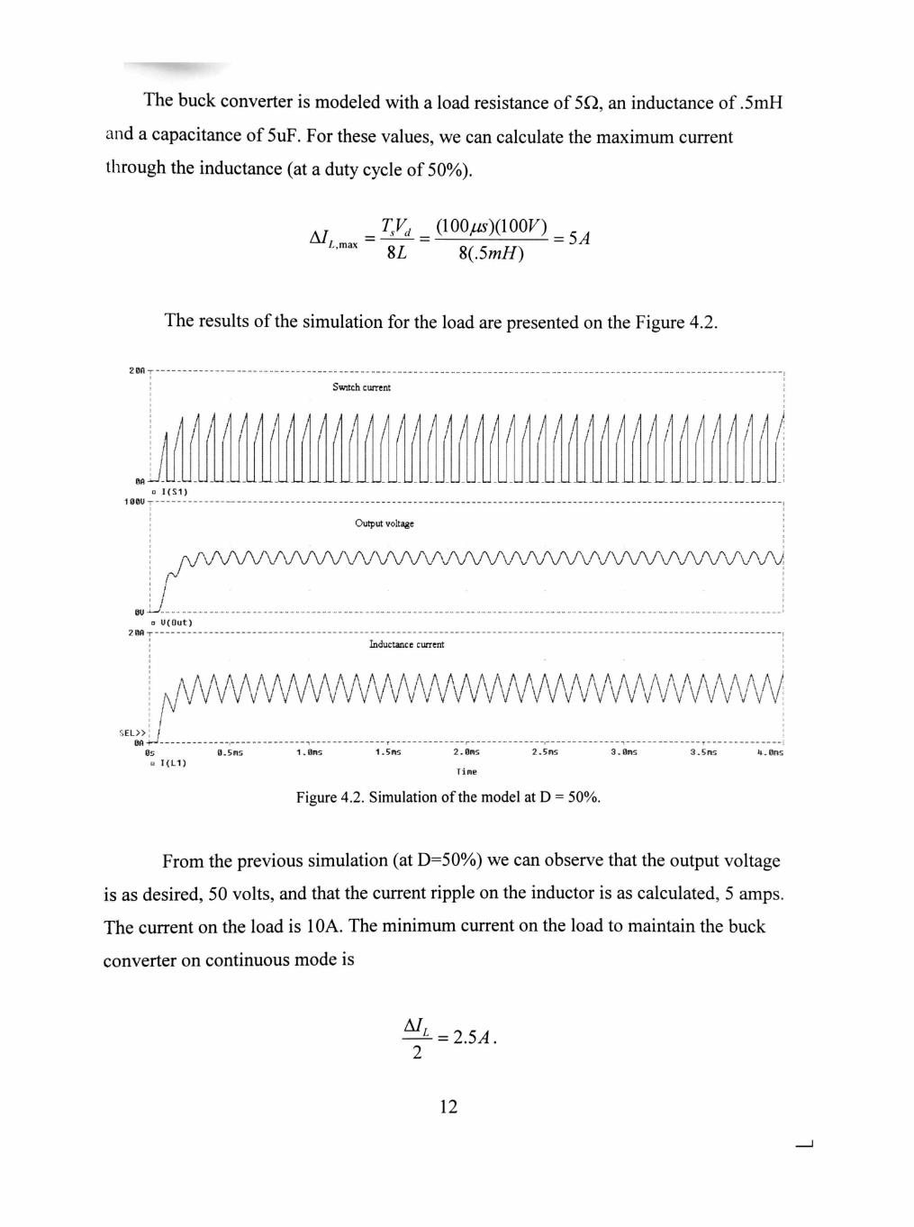
The buck converter is modeled with a load resistance of 5Q, an inductance of .5mH
and a capacitance of 5uF. For these values, we can calculate the maximum current
through the inductance (at a duty cycle of 50%).
^ ^Tf, ^{mjus)(mv)_^^^
' " " SL S(.5mH)
The results ofthe simulafion for the load are presented on the Figure 4.2.
2Bfl-
Switch current
BA u .1 /I /I ^ ,/\ ,i 1 /I ,-1 , U U,\ n,^ HL\ \u
° 1(S1) IBBUT
Output voltage
^^vAAAAAAAAAA/\AAAAAAA/\ / \AAAAA/\AA/vAAAAA^^ r
m ^-D U(flut)
ZBfl-r-Inductance current
i /V A/vVv^^/vWvVvVv^vvVvWv\AWM^A/vVvA^v SEL»: I
m-Os 0.5ns
" ICL1) l.Qms I.Sns 2.8n5
Tine
2.5n5 3.0n5 3.5n5 n.Bns
Figure 4.2. Simulation ofthe model at D = 50%.
From the previous simulation (at D=50%) we can observe that the output voltage
is as desired, 50 volts, and that the current ripple on the inductor is as calculated, 5 amps.
The current on the load is 1OA. The minimum current on the load to maintain the buck
converter on continuous mode is
AI, = 2.5 A
12
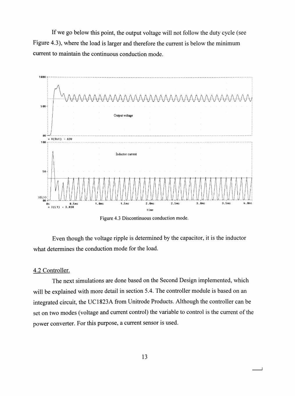
If we go below this point, the output voltage will not follow the duty cycle (see
Figure 4.3), where the load is larger and therefore the current is below the minimum
current to maintain the continuous conduction mode.
108U
BBU-I
V-
»U
i8n
''\''^j'mM\l¥AlW\fiJ\IW\PMf\f\fiAWWWm
Output voltage
• U(Out) •> 63U
0s a.5ns n i { L 1 ) » 3.83f l
3 .5ns Ji. Bns
Figure 4.3 Discontinuous conduction mode.
Even though the voltage ripple is determined by the capacitor, it is the inductor
what determines the conduction mode for the load.
4.2 Controller.
The next simulations are done based on the Second Design implemented, which
will be explained with more detail in section 5.4. The controller module is based on an
integrated circuit, the UC1823A from Unitrode Products. Although the controller can be
set on two modes (voltage and current control) the variable to control is the current ofthe
power converter. For this purpose, a current sensor is used.
13
4.2.1 Voltage mode configuration.
As previously said, although the configuration on the chip is set as voltage mode,
it was the current the variable to control. Figure 4.4 shows the configuration for the
control.
monitor
setpoint
Switch > control
signal Ramp
(a) Ramp
Control
(b)
Figure 4.4 Voltage control mode.
The amplifier uses the output current and the reference current to produce a
control signal, this difference is also known as the error. This signal is then compared
against a repetitive waveform to produce a width-modulated signal that is used to control
the switch (Figure 4.4b). When the output current approximate to the reference current,
the error decreases so as the width ofthe modulated signal.
Figure 4.5 shows the controller model used for the simulation.
Setpoint
O 0 0 0 > -sJ
R17 C12 r-AA^ 1 ^ —
5k .001 u
R15 •VAr-
10k
.001 u R16 •I I—^l—^^v-^
C11 1000
^ ^ - € 1 l J l £ t ^
;'a.
PVVM2 Q
"1
Input current
Figure 4.5 Voltage controller model.
14
The previous controller uses a reference current and the output current. The model
normalizes the output difference in order to have a stable PWM waveform. Figure 4.6
shows the complete model for the power converter.
Buck (Step-Down) Converter for Plasma Burner:
L13 P
500uH
Roff= 1000k R 0 ri= 1 m
R11
-V4-^ ^ S3
t R14 1
Figure 4.6 Plasma burner.
The load ofthe model consist of two resistance connected in parallel. One of them is
open and it closes at 2ms. This change on the resistance ofthe load is in order to observe
the control for variations on the load. The initial resistance is Rl 1 and then is change into
Rl 1//R14. The simulation ofthe model with a setpoint of 200A is shown on Figure 4.6.
B.Srrt 1.nn«; l -S i r ;
Figure 4.7 Current control with one module.
15

The error ofthe system is shown on Figure 4.8, where the error is minimized by
the controller.
8.81! -^ Y^"
-9.2V + •: lis O . ' J F K 1 . B
= U ( D l K K 1 : 0 U r ) - I)
Figure 4.8 Error signal.
It can be observed that the control behavior is very stable for the setpoint current.
The next step is to implement more than one controller in order to have more power and
to observe the behavior ofthe load with more than one power converter. Also the purpose
ofthe simulation is to observe the control with more than one setpoint. Another reason to
have three independent power converters with three independent setpoints is to protect
the modules from each other. In the event that one ofthe modules fails during the
operation, the other two would not have to compensate that loss, therefore suffering a
great stress in a short period of time. Figure B.l in Appendix B shows the converter for
three different power converters. It should be noted that in Figure B.l each model has an
inductance at the output and that they are connected to a single one on the load.
Figure 4.8 shows the results ofthe simulation for equal setpoints and with equal
output inductances. It can be observed that the control for this simulation is very stable
and that the output current is constant even with the change ofthe resistance.
16
J
Load current
Isetl = 200A Iset2 = 200A Iset3 = 200A
Us ll .Sns I .Uns I . S n s " 1(L2!( ) • K 1 2 6 ) I ( L 1 / ) » I ( L 1 3 )
2.DBS 2 .Sns 3.1)ns
T l M
3 .5ns ^ . l lns '4.!>iiis ?».8ns
Figure 4.9 Current control with three modules. Iset = 200A
Figure 4.9 shows the simulation for three different setpoints.
seofl
B.5ni> I.Bn-j 1 .SH; o I ( L 2 9 ) ' I ( L 2 6 ) K L W ) • I {L13)
Z.Sfli a.Bnii
Tine
<(.5iic> S.Oni
Figure 4.10 Current control with different setpoints.
The result for the previous simulations shows that the controller is stable for
ierent setpoints. This was an important issue, because in the event that one ofthe
17
modules could be disconnected abmptly due to a failure, the other modules could still
handle the same current without problem.
4.2.2 Current mode
The current control mode differs from the voltage mode on the feedback for the
PWM. The UC1823A can be configured for a maximum duty cycle, and in this case was
set for a maximum ofthe 80%. Figure 4.11 shows the model ofthe second control.
setpoint Switch ^ control
signal
A Setpoint ciArrent
.^•'^''^ I I I I 1
i i
^
- * -
t Max Duty Cycle
b)
Figure 4.11. Current control: (a) Controller, (b) PWM waveform
The current control for the chip differs from the first on the configuration on some
pins. Instead of comparing the difference ofthe actual current and the reference current,
the amplifier is set for unit gain and the actual current is connected to the comparator.
Whenever the actual current reaches or 'hit' the reference current, the PWM output turns
off and it is tumed on until the next cycle. Figure 4.12 shows the controller model
implemented on the module using a flip-flop.
18
U9A
DSTM2 |CLICJ-Lft>-
Jil^l 1A J. 14
-!C>
12
.13
^
i <f6 , Q H °°l Setpomt
' Tnmit' riirr
Reset
PWM1
Input current
Figure 4.12 Use of a flip-flop as the controller.
The controller for this module was implanted using a flip-flop type J K and a
comparator stage as in the first model. The flip-flop is configured to works as a counter
that changes the state ofthe output with each falling edge ofthe clock transition. In order
to resemble the operation ofthe controller, a maximum duty cycle ofthe 80% is
implemented with the use ofthe reset ofthe flip-flop. The clock transitions are the basis
ofthe controller. The clock uses two signals to fire the transitions, a single falling edge at
the beginning ofthe cycle and the error or difference from the actual current and the
reference current. Figure 4.13 shows the fiip-fiop control signals.
J A i
1 1 1 1 1 1 1 1 L
1 Figure 4.13 PWM control signals, (a) start, (b) reset and (c) clock signal.
In order to tum off the flip-flop whenever the current hits the setpoint is
accomplished by an analog to digital interface that consists ofthe difference between the
current and the setpoint normalized to clock signals from 0 to 5 volts. Figure 4.14 shows
the model used for a single power converter, and Figure 4.15 shows the result of
simulation for a 200A setpoint.
19
L12
V2
600V
aODuH IC=20
Buck (Step-Down) Converter for Plasma Burner;
? T 5DnH
L11
R
) L7 ' 5nH 1
136GuF IC=250V
C
4 L, V"
Ron.1Om i
9
icft^sov C13
1 auF
H 1 ,
D2 A
L17
lOOuH
R22 Roff=ioa(
I i) LI 3 "» " • "
* 2 > - v ^ - ^ ~ . K - 1 snnuH ! \ J V,..
R H I
DSTM3 y |cix_rut> ^
.^ . \ ^ Reset
.,> R14 ?©-
1
U9A
DSTM2 |CIXJ-Lft>-
-U-IJA gj..1.i
3
L-O
:'-fE6 -CM
12 ^
Reset
200
Figure 4.14. Current mode.
<»88-^-type A lOOuH 500uH 200A
/' *^"^^''^'*-^
n I ( L 1 3 ) « 20B 5 .eu-
SEL>> OU
8s 1 . O n s c U ( L I M I T 3 : I N ) > U ( L I M I T 2 : 0 U T )
2 . 0 n s
T i n e
3 . 0 n s J t .ans
Figure 4.15 Setpoint of 200A.
We can observe the trigger signal that turns off the controller when the current
; the setpoint. This control is also very stable for one module. On the Appendix B is
nded the controller used for two modules (B.2), where two separate inductances are
d to inject the current into a main inductance.
Different cases are simulated, where the values ofthe inductances and the setpoint
varied. The simulations were intended to observe the behavior ofthe model for
20
different sepoints and for different values at the inductance. Table 4.1 shows the cases
simulated
Table 4.1 Simulation cases.
Figure
4.16 4.17 4.18 4.19 4.20 4.21 4.22 4.23
L4
lOO^H
100|iH
lOO^H
lOOfiH
lOO iH
lOOiiH
110|iH
llO^H
L8
lOOiiH 100|iH
lOOnH lOO iH
llO^H
llO^H
llOnH
llO^H
L13
500^H
SOO iH 2^H
2^H
500^H
2fiH
500^H
2^H
Setpoint 1
200 100 200 100 200 200 200 200
Setpoint2
200 200 200 200 200 200 200 200
Figure 4.16 presents the case were two modules inject the current into the load. Both
modules present the same setpoint ant 200A and each module has an output inductance of
100|iH. The inductance for the load is of 500|iH. The control behaves pretty stable and
the ripple current is very low.
688-
2«a
.../
^^''
a-mnmmnnnonrfiiiJJJiLiiiiiiiiJiiJiiiiii JUU
8s 1.8ns 2.0ns 3.8ns c U(LIMn3:IH)»19 •^ U(LlMn6:lN)«12 I(L13) u 1(L8) .- KKt)
Tine
It. 0ms ; .ems
Figure 4.16. Equal setpoints and inductances.
Figure 4.17 presents the case where there is a difference on the setpoints. This
case presents an oscillation ofthe switches due to the difference. Once the module with
the lower setpoint reaches the desired current, it turns off, as desired. But when this
21
happens, the other module presents an increment of current in a short period of time, and
the inductor ofthe module tumed off presents a decrement ofthe same magnitude. This
oscillation decreases when the load resistance is reduced. This oscillation is even more
notorious by observing the duty cycle of both modules.
3U8n
280
lee n r i nn fW l j lA^ nj"^vr^^^-
/
taffiil 11 n n i i s 1 . ens 2 . Bras 3 . Ons
a U ( L l N I I 3 : i N ) » 5 « U ( L I M I T 6 : 1 H ) « 7 I ( L 1 3 ) . I ( L 8 ) c I ( L» i ) T i n e
ii.Bns S.eras
Figure 4.17. Different setpoints, equal inductances
Figure 4.18 present the case where the inductance load is smaller, of 2^H. This
represents a bigger current ripple. The systems is more stable because both modules
presents the same setpoint at 200A
6S0n
Hoe
288
' i r ' l i f, ^ I f i j: \ \ i i 'f. \ i, \ \ ^ ?• K '^^ \ \
i/S mmmm
r-= 8-1 mmnfmnfif\M!mhmmAiiiiJu\iMiu\n\uuiiu
es 1 . Onii 2 . ens 3 . Sns u « { L I M 1 T 3 : I N ) » 5 - U ( L I M I T 6 : I N ) « 7 I ( L 1 3 ) * 1 ( L 8 ) o I { L l t )
T i n e
I t . 8ns 5 . 8 n s
Figure 4.18. Low load inductance
22
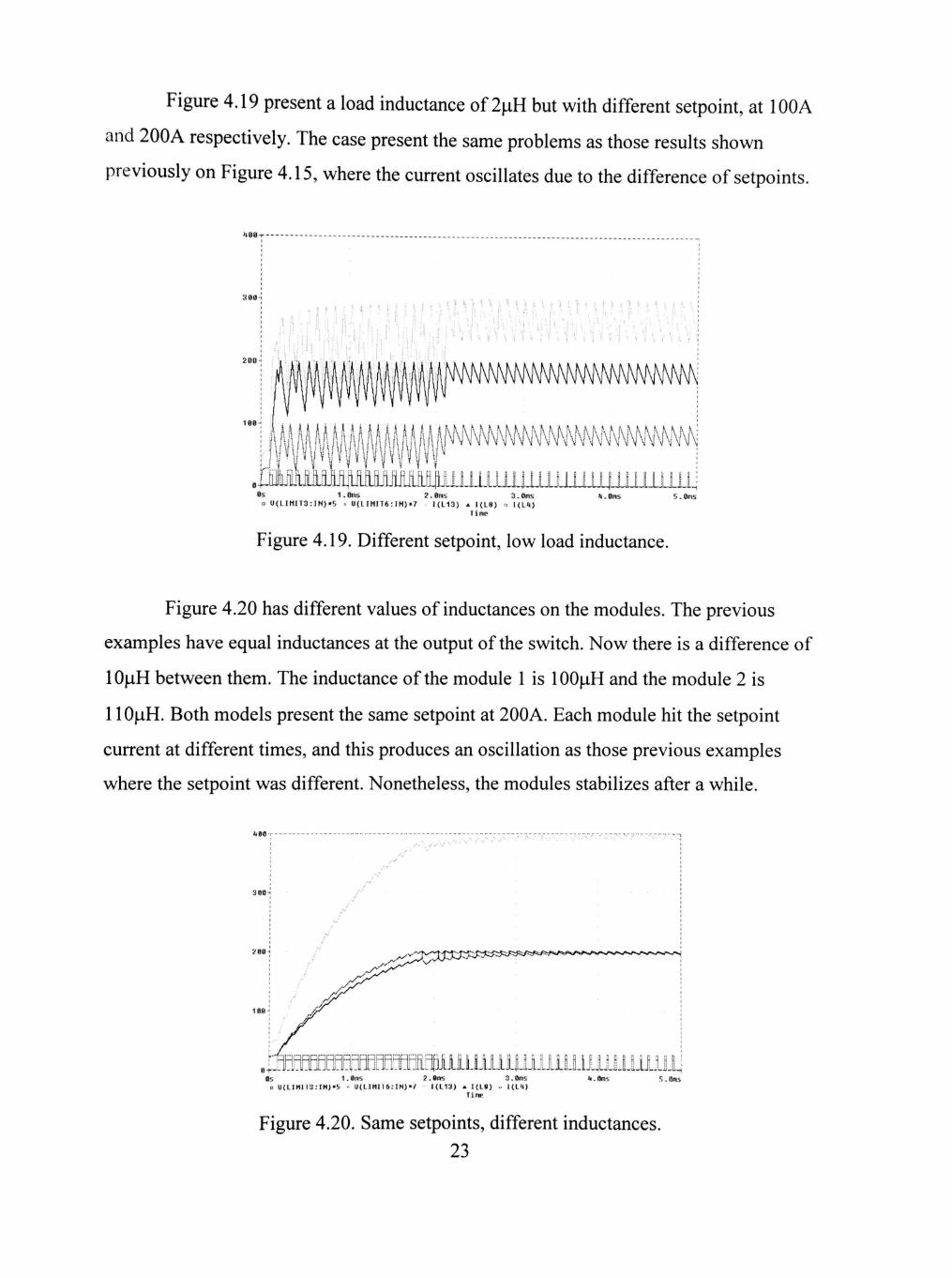
Figure 4.19 present a load inductance of 2|iH but with different setpoint, at lOOA
and 200A respectively. The case present the same problems as those results shown
previously on Figure 4.15, where the current oscillates due to the difference of setpoints.
388
288
! i i M
85. 1 . Bi!i!i 2 . 8ms 3 . Ons * , Ons o U ( H I H T 3 : I N ) . 5 . U (L IM1T6 : IH )« / 1(110) * l ( L 8 ) o l(Li<)
l ine
Figure 4.19. Different setpoint, low load inductance.
Figure 4.20 has different values of inductances on the modules. The previous
examples have equal inductances at the output ofthe switch. Now there is a difference of
10|aH between them. The inductance ofthe module 1 is lOOjiH and the module 2 is
110|uH. Both models present the same setpoint at 200A. Each module hit the setpoint
current at different times, and this produces an oscillation as those previous examples
where the setpoint was different. Nonetheless, the modules stabilizes after a while.
188-;
.IlBTfflfflBliflfflfflaaMilllliiilJlliiUi 9<; I . Dm 2. •« ; 3. 8n"j o U(LIMlia:IH)>!, - U(LIHil6rIN)"/ 1(L13) .. I(LS) ., l(L'l)
Tine
',. nm
Figure 4.20. Same setpoints, different inductances.
23
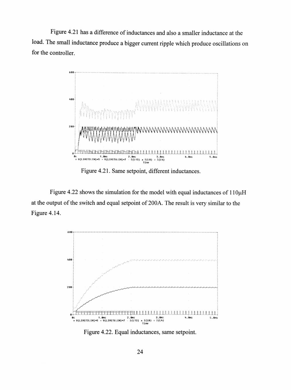
Figure 4.21 has a difference of inductances and also a smaller inductance at the
load. The small inductance produce a bigger current ripple which produce oscillations on
for the controller.
6 8 8 ^
lee^
288
n M :\ .
:n n u M M
0 +
wmwmmmmmmmm
MHOtiPtiDMMliLl!^ imuxii 1 . ens 2 . Bins 3 , 8ms
n U ( I . I M I T 3 : I N ) . 5 ^ U ( L i m T 6 : I N ) » 7 1(1.13) » 1(1.8) o I ( l . i i ) T i n e
S. Ri9S
Figure 4.21. Same setpoint, different inductances.
Figure 4.22 shows the simulation for the model with equal inductances of 110|iH
at the output ofthe switch and equal setpoint of 200 A. The result is very similar to the
Figure 4.14.
688-1
288
y-,y'
y
, / , /
aBfflRHnmp[1±iHi:HIT]a.i...ftJ..^^ Ss 1 . 8 n s 2 . 8 n s 3 . Ons
D U ( L I M 1 T 3 : 1 N ) » 5 » U ( L I M I T 6 : 1 N ) « 7 1 ( L 1 3 ) A I ( L 8 ) C K L I ) T i n e
t.Uns S . 8 n s
Figure 4.22. Equal inductances, same setpoint.
24
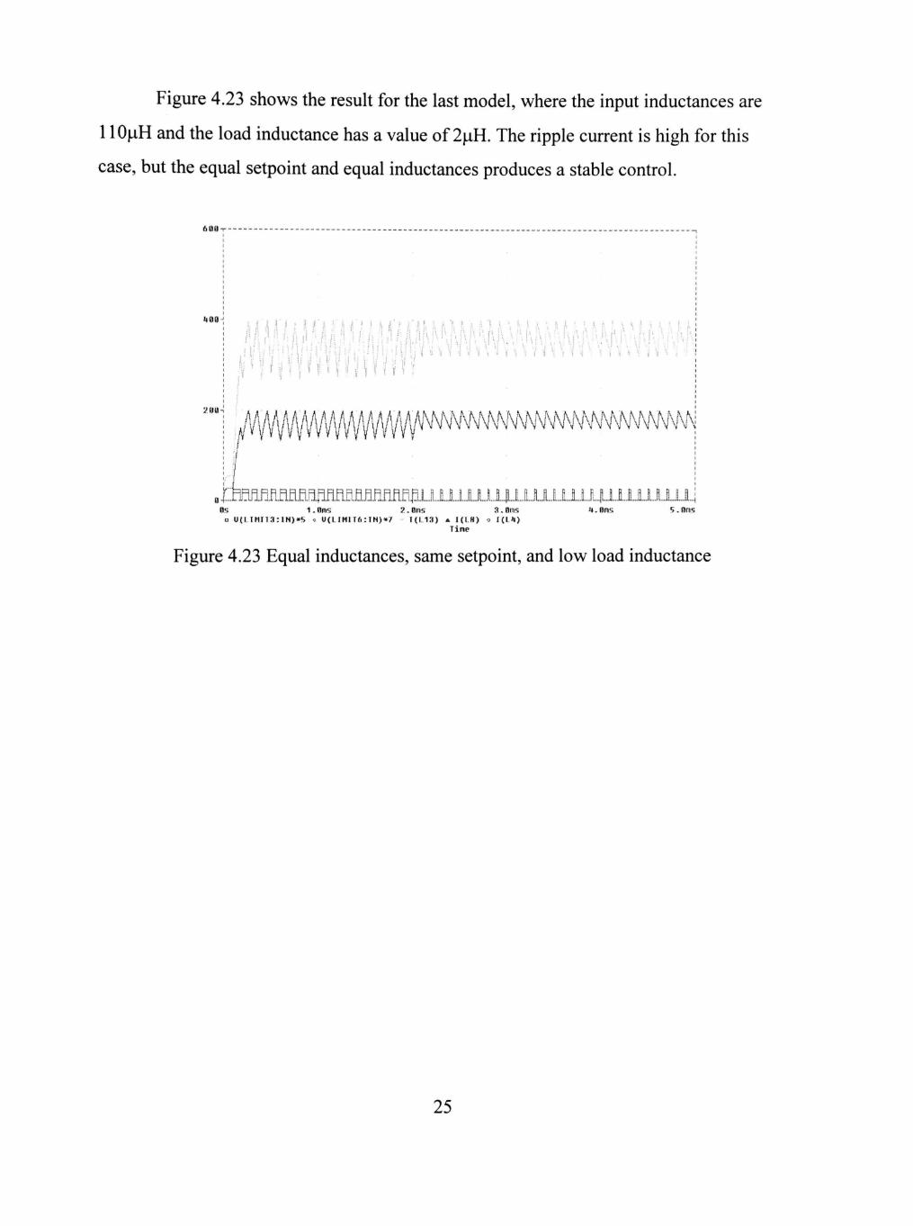
Figure 4.23 shows the result for the last model, where the input inductances are
110|LiH and the load inductance has a value of 2)aH. The ripple current is high for this
case, but the equal setpoint and equal inductances produces a stable control.
6 U 0 - r -
KSO
2nu
A r i ; . I f h y s I ' ^ \ I'' r H ,
F ;M n
\ i i i ?- I \ \ ^, I i^ \ \ i, t \ i ^ I \ \ \ \
1 5 V '1 < ^ ? •: '• i' 1 1 "i 'i ^ '• ? i i ^ N j *
l^'l^%^^^^'^^f^^mM^mmm^mmmi^
thimHiiflflmpmHflmflflfl&ujiiJjjj.|j.iiJ±iJjjjJiiJiJjjjJ OS 1 .Bns 2.8ns a.fliiis u U(l IMn3:lN)»S « 0 ( l IH I t6 : IN )»7 1(113) » l ( l .«) •> 1(1.'t)
Tine
t.Bns 5. Bills
Figure 4.23 Equal inductances, same setpoint, and low load inductance
25
CHAPTER 5
IMPLEMENTATION
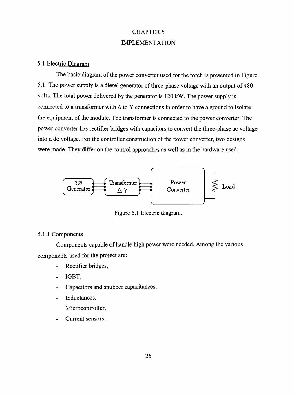
5.1 Electric Diagram
The basic diagram ofthe power converter used for the torch is presented in Figure
5.1. The power supply is a diesel generator of three-phase voltage with an output of 480
vohs. The total power delivered by the generator is 120 kW. The power supply is
connected to a transformer with A to Y connections in order to have a ground to isolate
the equipment ofthe module. The transformer is connected to the power converter. The
power converter has rectifier bridges with capacitors to convert the three-phase ac voltage
into a dc voltage. For the controller constmction ofthe power converter, two designs
were made. They differ on the control approaches as well as in the hardware used.
30 Generator I •
i Transfomier; AY
Power Converter Load
Figure 5.1 Electric diagram.
5.1.1 Components
Components capable of handle high power were needed. Among the various
components used for the project are:
Rectifier bridges,
- IGBT,
Capacitors and snubber capacitances,
Inductances,
Microcontroller,
Current sensors.
26

The rectifier bridge used is the model SKD160 from Semikron. This rectifier
bridge is capable of handle up to 160 amperes of current. The estimated input current
from the power supply was calculated on 450 amps. Three SKD160 units were used in
two different configurations. Figure 5.2 shows the rectifier bridge (internal diagram).
A u nf .
a) b)
Figure 5.2 Rectifier bridge: (a) symbolic and (b) internal diagram
The switch used on the project was the insulated gate bipolar transistor (IGBT). The
IGBT SkiiP 1442 GAR 120 from Semikron was used due to it high capacity to handle
current. It IGBT can handle up to 1200 volts and 560 A rms at a maximum switching
frequency of 14 kHz. The IGBT is a switch controlled by voltage. The internal block
diagram of one IGBT is shown in Figure 5.3. We can observe that this model includes the
diode connected to ground, which simplifies the hardware on the buck converter.
V—P—^—^ l=\ JhV 1^
- f?^ -^Tv-
- T ^
f t f f Driver
-o o—I -O O 1 ^
-o o—I
Figure 5.3 IGBT SkiiP 1442. Buck converter
27

To make the capacitor bank, several models were used, but for the final design the
85uF capacitor from 'Electronic Concept" was used. This capacitor can handle up to
1000 volts of dc.
Two different companies fabricated the inductors. Two inductors of 110 jaH were
designed by MTE Corporation. Each inductor drives 600 volts of AC or 1000 volts of
DC. Another two inductances from Norlake were used. One of them has a value of
lOOuH and the second one is 500|LIH.
In order to have a ground for the equipment, a transformer made by Mitran in
configuration A to Y was used. The input voltage is 460 +/- 5% and the output current is
460Y/266 A.
To measure the input and output current, current sensors from F. W. Bell were
used, the CLN-1000 and the CLN-300. Each one can measure up to lOOOA and 300A,
respectively.
5.2 Microcontroller HC12
The MC68HC912B32 (68HC12) microcontroller unit is a 16 bit device composed
of standard on-chip peripherals including a 16 bit central process unit (CPU 12), a 32-
Kbyte EEPROM, a 1-Kbyte RAM, a 768-byte EEPROM, an asynchronous serial
communication interface (SCI), a serial peripheral interface (SPI), an 8 channel timer and
16 bit pulse accumulator, an 8 bit analog to digital converter (ADC) a four-channel pulse
width modulator (PWM), and a J 1850-compatible byte data link communications module
(BDLC) [9]. This microcontroller has eight ports from which seven can be configured as
input-output.
For this project most ofthe ports were used as input and output ports, but a basic
emphasis is set on to two ports, the PWM module port and the analog to digital converter
port. The use of a keyboard and a Liquid Crystal Display were implemented with ports A,
B and T.
28

5.2.1 PWM Module
The 68HC12 microcontroller from Motorola has a PWM module that allows us to
drive precise waveforms with hardware instead of software. The pulse width modulator
(PWM) subsystem provides four independent 8-bit PWM waveform or two 16 bits PWM
waveform or a combination of one 16-bit and two 8-bit PWM waveforms. Each
waveform channel has a programmable period and a programmable duty cycle as well as
a dedicated counter. A flexible clock select scheme allows four different clock sources to
be used with the counter. Each ofthe modulators can create independent, continuous
waveforms with software-selectable duty rates from 0 to 100% percent. The PWM can be
programmed as left-aligned outputs or center-aligned outputs [9].
One advantage ofthe HC12 is that the duty cycle is easily controllable with one
register. The generated PWM waveform with the HC12 is as follows. It is a left-aligned
signal with a frequency of 10 kHz, a variable duty cycle and has positive polarity. Figure
5.4 shows the resulting waveform.
h«-Duty-H t=.1ms = 1/10 kHz
Figure 5.4 Left aligned waveform, positive polarity.
To program the desired frequency, some register need to be declared. As said before,
we can have 4 independent channels of 8 bits or two channels of 16 bits. Because the
application requires more than 2 outputs, the first option was chosen.
The PWM systems uses the E clock as its primary clock source. From this primary
source, it branches into two separate clock chains, clock A and clock B. Clock A drives
channels 0 and 1 and clock B drives channels 2 and 3. Both clocks are connected to E
through prescalar chains. The job ofthe prescaler is to divide the E clock. The clock A
and B can be connected into a second prescalar, SO for clock A and SI for clock B.
PWPOL allow us to select the second prescalar. The formula for SO is as follows:
29
Clock A = PWCLK{7> hits)
Clock tSO = ClockA
2*{PWSCAL0 + \)
The same applies for SI, but using clock B and PWSCALl, This formula indicates
that we can divide the clock by multiples of two with the second prescalar. Once we have
selected the clock source, we have to select the alignment ofthe channel. Figure 5.5
shows the PWM clock chain.
PSBCK PS8CK IS BH 0 OF PWCTL UEGISIER. INItKNALSlGNALi/WfiOAIlSl If- IHt MCU iS IN 8M:KG!K)UND DEBUG MOOL
CLOCK A
ECLK
0:0:0
0.0:1
0:0:0
0:1:0
0:0:1
0:1:1
0:10
+ 2
1:0:0
0:1:1
-5-2 1:0:0
1:0:1 •*-2
1:1:0
1:0:1
^2
1:1:1 + 2
1:1:0
1:1:1
8-B!! UOV^NCOLJNitR
PWSCNIO
1
= 0
8-BIT SCALE REGISIER
PWSCALO ^ 2
CLOCKB
BITS: PCK82, PCKB1. PCK80
REGISIER: PWPRES
BUS: PCKA2, PCKA1, PCKAO
a BIT DOWN COUNIEP
PV/SCNll
1
= 0
8BI1 SCALE [REGISTER
PWSCALl + 2
•CLOCK SO - {CLOCK A)/2. (CLOCK A)M, (CLOCK A)/6..,, (CLOCK A)/512 "CLOCK SI - (CLOCK 8)/2. (CLOCK B)/4, (CLOCK B)/6..„ (CLOCK B)/r,12
Figure 5.5. PWM clock chains
• - * '
o
q
T
CLOCK TO l-AVM CHANNEL 0
CLKO
J
CLOCK TO l>WM CHANNEL 1
PCLK1
o o
><
T
CLOCK lOPV/M CHANNEL 2
PCLK2
X
T
CLOCK 10 PWJI CHANNEL i
PCLK3
30
The HC12 has the option to select either left-aligned or centered-aligned output. In
this project left alignment was selected to simplify the deduction ofthe formulas to
achieve the desired frequency. Figure 5.6 shows the block diagram ofthe PWM left
aligned module.
CLOCK SOURCE (ECLK)
^^ P*
CLOCf
CJMfc
.EDGt S YNC
i
1 1
1 1
1 WENx
' PPOL ^ 0
PPOL-1
CENIR
PWCNlx
RESt 1
- 0
FROM POP r p DAI A REGISIER
UPCOUNItRONLY
- * "
8-Bll COMPARE
PWDlYx
8-BIIC0f<(PARE^
PWPERx
S
Q
R
MUX
i k
- * - PWDIY - ^
* • •
^
MUX
i
• POLx
_ FIWPLR
i
fOPIN DRIVER
Figure 5.6. PWM left aligned output channel.
The last step it is to set the period ofthe waveform and the duty cycle. The PWM
channel work as follow. The PWCNTx register (counter) will start counting up. When
PWCNTx is equal to PWDTYx (duty cycle), the output bit is set accordingly to the
polarity, but PWCNTx will continue counting up. When PWCNTx reaches PWPERx
(period), PWPERx causes the output bit to be reset, and also causes PWCNTx to be reset
to zero, then starts again.
It is important to note that the resolution ofthe duty cycle depends on the value of
PWPERx. The larger the PWPERx value, the more accurate the duty cycle can be
adjusted. In order to have this, the period needs to be as large as possible.
For this project, the frequency ofthe signal was selected to be lOkHz. The clock A
and B was set for 2MHz (prescalar of 2 on PWCLK). Clock SO and SI were not used.
The PWPER set for 200d (out of 255d). The formula is as follows:
31
Clock _ A
ChannelFreq
SMHz
PWCLK Clock _ A
PWPER
4 2MHZ
200
= 2MHz
= \OkHZ
According to the previous formulas, the maximum resolution ofthe duty cycle is
0.5%. We can consider as a disadvantage the selection ofthe frequency subjected to the
resolution ofthe period, because we have to sacrifice the period for a precise waveform.
5.2.2 Analog-to-Digital Converter (ATD)
The purpose ofthe Analog-to-Digital Converter (ATD) is to allow the HC12 to
read voltages as 8 bit binary numbers. The HC12 has 8 channels of 8-bit A/D and it is
possible to configure them for a 10 bit resolution. Figure 5.7 shows the block diagram for
the ATD.
o
i i a 5 - J
S :3
RCDACA8RAY AND COMPARATOR
u SAR
A? 00
AIDt V i
A1D2
Us fv l AID3
rv A!W
U \ rV AIDS
AIDS
liNf A1D7
ANALOG MUX ANO
mpunm
POSIAjaOATA iNRJi R L a s r t R
T"
ClOCK SLlta>?>Ri:SCALt
iz u iz
VcDA
AN7^)\07
AM&4^AD&
AMS^AOS
AM4*'AC4
A?4J.4'AD3
A^Tjrt'AtX)
A (NILRNALBUS
V
Figure 5.7 Analog-to-Digital Converter.
32

The module has two modes: single mode and multichannel mode. The single
mode takes eight sequential readings from a single channel. The result ofthe 8 samples is
stored from ATDO to ATD7. In the multichannel mode each input channel is selected and
one sample is stored on the result register. The result from channel 0 is sent to ATDO,
channel 1 to ATDl and so on through channel 7. Most ofthe control bits are in the
register ATDCTL5. With the bit SCAN, we can mn continuously samples ofthe
channels, each one independent from each other. Bit 4 on ATDCTL is called MULT and
set for multichannel mode.
For this project, more than one analog input was estimated, therefore the work
focused on the multichannel mode. The bit SCAN was also set to have continuous
conversion from the input channels.
5.2.3 Keyboard
Although the keyboard is not a module ofthe microcontroller, it is explained here
because ofthe connection with the microcontroller. The use of a keyboard is practical as
an interface user-system. A common keyboard is the matrix type, which saves the amount
of I/O pins used to implement it. Each key has it own combination of row and a column
wires. Figure 5.8 presents the internal diagram ofthe keyboard used on the board.
Column 1 Column 2 Column 3 Column 4
1 1(1) 21(2) 3|(3) A | ( ^
PAD t>- 1 im
PAl o- I
PA2 o-
7|(g)
PA3 o-
*l(l^
PA4 o-
I im I SJOU) O O-H
OKI'!)
i
PA5 o-
1 M(7)
9 1(11)
#Ja5)
PA6 o-
J B|(g)
J ^ C|(12)
J ° Dj£<5)
PA7 o-
Rowl
Row 2
Row 3
Row 4
Figure 5. 8. 4 x 4 Matrix Keyboard.
33

It shows a 16 key matrix keyboard. Each key has a momentary contact switch that
is connected to an intersection of a row and a column. When a key is pressed, the switch
makes a momentary connection that causes a short circuit between the row and the
column. When the key is released, the open circuit exists again between all wires. To
determine which key is pressed, the microcontroller must scan the rows and columns to
identify the row and column intersection ofthe short circuit. Each key has an identifying
number.
To identify the key code, the microcontroller scans each contact in sequence, and
increment a counter each time it scans the next key. When it detects a closed contact, the
counter is stopped and it has the corresponding key code. If no closed contact is found,
the key code is reset to zero. This process is called keyboard decoding [10].
To detect a short circuit, the HC12 drives one ofthe output lines low and checks a
corresponding input line. If it is also low, the key was pressed. If the key is not pressed,
the open circuit allows the resistor to pull up the input line into a logic one. For example,
to check key code 8, the HC12 drives PA2 low and checks the input at PA5. If PA5 is
low, then the key was pressed. To save hardware, the port A has the option to activate a
intemal pull up resistance, so for the design it was not necessary to set external resistor
connected to Vdd. Figure 5.9 shows the diagram used to connect the keyboard to the
HC12. It can be noted that also the connection for the reset was set.
PA1 o-PA2 0-PA3 0-P M O -P/56 0-PPflO-PA7 0-
RESETO
4
Pkey,
« -
Figure 5.9 Schematic keyboard connections.
The basis ofthe program for the keyboard was based from [10]. Two main
subroutines are developed, getkey and breakkey. Getkey waits for a key to be pressed and
34

saves the value ofthe key and breakkey waits for the key to be released. The scan
procedure is done using a look-up table. It was necessary to use a debounce routine to
avoid accidental bounces from the keypad.
The table 5.1 shows the keys and their code.
Table 5.1. Input keyboard for the matrix board.
Key Code
1 2 3 A 4 5 6 B 7 8 9 C *
0 #
D
Row
1 1 1 1 2 2 2 2 3 3 3 3 4 4 4 4
Column
1 2 3 4 1 2 3 4 1 2 3 4 1 2 3 4
Port A data (binary) 1110,1110 1101,1110 1011,1110 0111,1110 1110,1101 1101, 1101 1011, 1101 0111, 1101 1110, 1011 1101, 1011 1011, 1011 0111, 1011 1110,0111 1101,0111 1011,0111 0111,0111
Port A data (hex)
EE CE BE 7E ED CD BD 7D EB CB BB 7B E7 C7 B7 77
Although this is the table used for the key scan, it is important to define the order
ofthe key code for the look up table, because the counter is linked with the symbol ofthe
key pressed. Every time the scan starts, it begins with the counter on zero. If the key
pressed is 3, that key will be checked until the counter reaches 3. It s important to observe
the order ofthe values on the look up table. For the keyboard program, there were 4 basic
subroutines, keybo, getkey, breakkey and idkey. The listing pseudocode used for the
keyboard is show next.
; Pseudocode for matrix keyboard driver keybo:
call getkey ; call breakkey ; return ; The result is saved on ACCA
getkey getkeyl
call idkey if counter = 16d repeat getkey ;only 16 keys
35
save key call idkey if actual key = prev key
then return else repeat getkeyl
breakkey breakkeyl
call idkey if counter <> 10, repeat breakkeyl return
idkey
idekeyl keypointer = 0, counter = 0
portA = *keypointer if portA == *keypointer
return increment keypointer & counter if counter < maxcounter
then repeat idkeyl return
if the counter has a number then repeat util key released
clear the pointer and the counter write the key code on portA then read portA, if equal, then a key was pressed
5.2.4 Liquid Crystal Display
Like the keyboard, the liquid crystal display is not a part ofthe microcontroller.
However, it is explained here as part ofthe modules. For the display ofthe data acquired
on the project it was necessary to use a Liquid Crystal Display (LCD). The model used is
the Seiko L4034 4X40 LED Backlight LCD with the HD44780 as the controller chip.
The LCD has two controllers since each one control only two rows, and the LCD has four
rows. This chip is a special purpose LCD controller; it simplifies the work ofthe
microcontroller. This LCD is a simple but reliable because it requires minimum hardware
connections and the rest it is done with software. The communication with the LCD is
parallel and requires eight pins to write the commands, two to for the control signal and
two more for the clock signal. The LCD requires a control signal to set either characters,
the position ofthe cursor or in general to execute the LCD commands. Figure 5.10 shows
the diagram ofthe connections for the LCD.
36
DB7 O-DB5 O-DB3 O-DB1 O-E1A O-RS O-
•Ih-E1B O-Vdd o-
2 4_ 6_
10 H 12_
1? Ii 15 16 n i£ 19 20
-ODB6 -ODB4 -ODB2 -ODBO -O R/W
Vdd Q
R20
VIcA
-O Vdd Led-A
V R21
Figure 5.10 LCD Connections
The LCD works through the HD44780 controller, which has two 8 bit registers,
an instmction register (IR) and a data register (DR). The IR stores instmction codes such
as display clear and cursor shift, address information for display data RAM (DD RAM)
and character generator RAM (CG RAM). The DR temporarily stores data to be written
into the DD RAM or the CG RAM and data to be read out from the DD RAM or the CG
RAM
The DD RAM stores displays data represented in 8-bit character codes. Its
capacity is 80x8 bits, or 80 characters for each controller. The DD RAM address is set in
the Address Counter (AC) and is expressed in hexadecimal. Figure 5.11 shows the DD
RAM address for a 40-character x 4 lines display.
1 Istline
cont?ollet( 2nd line
2nd r i « ^ ^ controller \ 2nd Hne
00
40
00
40
01
41
01
41
26
66
26
66
27
67
27
67
DDRAM address (hex)
Figure 5.11 Address lines on the LCD
The pins DBO to DB7 write the character or the command to be displayed or
executed. El A and R/W are the control bits for the purpose ofthe word control. The
instmction set for the HD4478 is as show on table 5.2
37
Instmction Clear display Return home Entry mode
Display ON-OFF Cursor and display
Shift Function set Set CG RAM
address Set DD RAM
address Read busy flag
Write data to CG or DD RAM
Read data from SG or DD RAM
RS 0 0 0 0 0
0 0
0
0 1
1
R/W 0 0 0 0 0
0 0
0
1 0
1
Table 5.2 Instmction set
DB7 0 0 0 0 0
0 0
1
BF D
D
DB6 0 0 0 0 0
0 1
A
A D
D
DB5 0 0 0 0 0
A A
A
A D
D
DB4 0 0 0 0 1
DL A
A
A D
D
DB3 0 0 0 1
s/c
N A
A
A D
D
DB2 0 0 1 D
R/L
F A
A
A D
D
DBl 0 1
I/D C *
*
A
A
A D
D
DBO 1 *
S B *
*
A
A
A D
D
A best description of each instmction can be found on the technical data ofthe
HD44780. For the execution ofthe instmctions it is necessary to send a pulse of a
constant time to the pin E ofthe controller. The time pulse depends on the instmction.
For example, clear display and Retum Home require a pulse of 1.6 ms, and the rest only a
pulse of 120^s. As long as two different LCD were used, and each one having two
controllers, four different clock signals were required. To work properly with the LCD, it
is necessary to define some bits
1. Display clear 2. Function set
3. Display ON/OFF
4. Entry mode
5.3 First implemented design
DL = 1 N = 0 F= 0 D = 0 C = 0 B = 0 l/D = 1 S = 0
8 bit interface 1 line display
5x7 dot character font Display off Cursor off Blink off +1 (increment mode) No shift
The objective ofthe first design was to control the output power ofthe power
converter. It used IGBTs, capacitors, rectifier bridges and current sensors. Figure 5.12
shows the block diagram for the power converter.
38
30 Power supply
Rectifier Capacitor bridge bank
Buck converter
1 T
Y^ Load
Figure 5.12. Block diagram.
The power converter uses a rectifier bridge and capacitor bank to rectify the 3 0
voltage at the input and IGBTs as the electrical switches for the buck converter. The
output voltage is connected to the load. Although the objective ofthe above configuration
was the control of power, at the end it was for the control of current on the load. A more
detailed diagram ofthe above configuration is shown in Figure 5.13. In order to control
the buck converter, current sensors and the microcontroller 68HC12 from Motorola are
used.
SKD160
30
SKD16D
SKD16Q
± Isenl
SKiiP1442
\J: a
± Isen2
SKiiP1442
68HC12
+
V.
SKiiP1442
Figure 5.13. First design of electrical diagram
In this configuration, the rectifier bridges and the Buck converters are connected
in parallel. The capacitors at the input are used to release stress over the power supply.
39

The output of each sensor is connected to the 68HC12. For this design, the 68HC12 is the
controller ofthe power converter.
5.3.1 Interface boards
For the control ofthe power converters with the 68HC12, it was necessary to
design and constmct two boards to interface the microcontroller with the IGBTs and with
the current sensor (Figure 5.14).
\ ^
V^ ^
^
a A
Controller board
+ f^ut
A/D interface
Microcontroller HC12
Figure 5.14. Interface board with the HC12
The design ofthe first board was based on optocouplers. The optocoupler has two
purposes: to isolate the power supplies and to adequate the voltage levels from the
68HC12 and the IGBTs. The microcontroller work with voltage levels of zero and five
volts and the SKiiP uses voltage levels of zero and fifteen volts. Figure 5.14 shows the
configuration to adequate the voltage levels. The optocoupler used are the HCPL2232
from Agilent Technologies.
2.2k
o +15Va
o Topi
o Top2
o GND
Figure 5.15 Configuration for the optocouplers.
40

The purpose of this interface was to protect the microcontroller from the IGBT's
in case of a failure and to provide an adequate voltage level to fire the IGBTs. The
necessary voltage to trigger the IGBT's is 15 volts, and the output voltage from the HC12
is 5 volts. The optocouplers solve the problems, by isolating the voltage sources and also
coupling the signals. Figure 5.14 shows the configuration to adequate the voltage levels.
The optocoupler used are the HCPL2232 from Agilent Technologies.
The Appendix C shows the complete schematic used for the interface as well as
the board for the connections. Figures C.l and C.4 shows the boards used for the first
design.
On the first design, to measure the output current three different current sensors were
used. To reject the switching noise the current sensors were filtered with a lowpass filter.
The configuration ofthe filter is presented on Figure 5.15. The filter is a Buttherworth of
second order using an operational amplifier TL074A from Texas Instmments. The
current sensors were configured for a voltage level between 0 and 5 volts in relation with
current levels from 0 to lOOOA. For this reason, a unit gain was set for the filters. The cut
off frequency for the filter is 100 Hz. This is done to have a signal as smooth as possible.
Figure 5.16 Lowpass filter
The Appendix C shows the complete diagram for the analog to digital interface
used on the project, it also include the diagrams used for the boards implemented. The
design ofthe filter was simulated on Simplorer, and the response so as the result is shown
on Figure 5.16.
41
S1 lai
.22u
10M.
^K•
2Dk
10k -cn—r
a= 4) .101
LM3101
a)
0 \M-
VM1
b)
Figure 5.17 Filter design using Simplorer: (a) model; (b) simulation
5.3.2 Control approach.
The design ofthe controller based on the 68HC12 for the first design involves the
use ofthe PWM module. The techniques described here for the control use a PWM
constant signal at 10 kHz were the variable to control is the duty cycle. First the control
was intended to be for power. But at the end it focused on the control ofthe current. A
brief description ofthe controller is presented along with the code and simulations on
Simplorer.
5.3.2.1 Increment-decrement control. The first control implemented was an increment-
decrement control, where the variable to control is the current and the control action is
taken on the duty cycle. Figure 5.17 shows the flow chart used for the algorithm. The
control takes the value ofthe current and compare it against the setpoint. Depending on
the value, an action is taken, either increment the duty cycle if the current is below the
setpoint or decrement if the current is above. This control was used to test the IGBTs on
the early stages.
42

Decrement Dty
No
Figure 5.18. Increment-decrement
The pseudocode for the program implemented on the 68HC12is shown next.
; Increment-decrement control
define setpoint read current if current < setpoint
then inc Dty else dec Dty
repeat control
For this stage ofthe project, the 68HC12 test board designed by Dr Giesselman
was used. The setpoint was set using the potentiometer ofthe board.
As previously described, the ATD has a resolution of 8 bits. For this reason the
resolution for the current sensor on the HC12 for those voltage provided by the previous
configuration is of
10004
255b = 3.90A/bit
As we can see, the resolution is low if we try to keep control over a few amps. At
this point, simulations using Simplorer was done for a single branch (Figure 5.18). It can
be noticed that there are no capacitors at the output. As long as the load is soil, there is no
need to filter the output voltage. The main concern is to control the current on the
inductance.
43
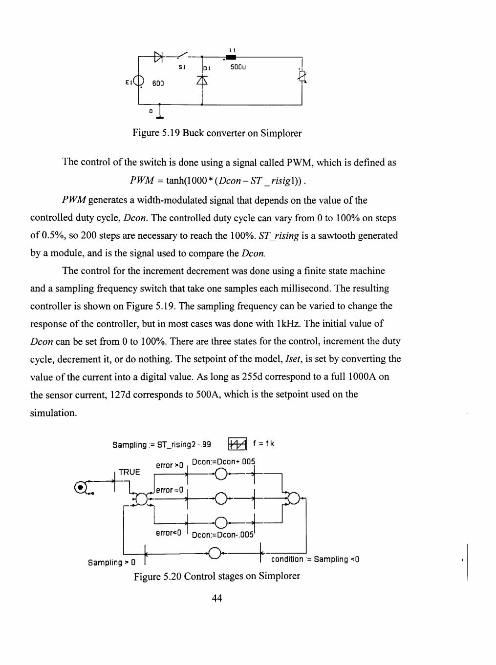
Figure 5.19 Buck converter on Simplorer
The control ofthe switch is done using a signal called PWM, which is defined as
PWM = tanh(l000 * {Dcon -ST_ risigl)).
PWM generates a width-modulated signal that depends on the value ofthe
controlled duty cycle, Dcon. The controlled duty cycle can vary from 0 to 100% on steps
of 0.5%, so 200 steps are necessary to reach the 100%. STrising is a sawtooth generated
by a module, and is the signal used to compare the Dcon.
The control for the increment decrement was done using a finite state machine
and a sampling frequency switch that take one samples each millisecond. The resulting
controller is shown on Figure 5.19. The sampling frequency can be varied to change the
response ofthe controller, but in most cases was done with IkHz. The initial value of
Dcon can be set from 0 to 100%. There are three states for the control, increment the duty
cycle, decrement it, or do nothing. The setpoint ofthe model, Iset, is set by converting the
value ofthe current into a digital value. As long as 255d correspond to a fiill lOOOA on
the sensor current, 127d corresponds to 500A, which is the setpoint used on the
simulation.
Sampling :=ST_rising2-.99 H H f:=1k
®:"n TRUE
error >Q Dcon:=Dcon+.0G5
error =G O O J>\ •o
Sampling > 0
error<0 Dcon:=Dcon-.005
O E
condition - Sampling <0
Figure 5.20 Control stages on Simplorer
44
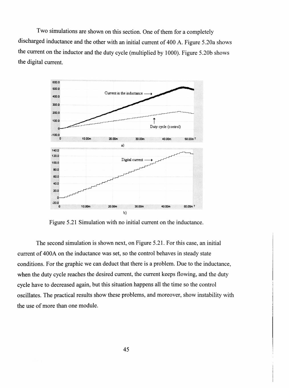
Two simulations are shown on this section. One of them for a completely
discharged inductance and the other with an initial current of 400 A. Figure 5.20a shows
the current on the inductor and the duty cycle (multiplied by 1000). Figure 5.20b shows
the digital current.
•1000 1D.0Dm 2Di30m 30.D0m 40.00m SQ.OOm T
10.00m 20.00m •X.Wm 40.00m SDXJOmT
b)
Figure 5.21 Simulation with no initial current on the inductance.
The second simulation is shown next, on Figure 5.21. For this case, an initial
current of 400A on the inductance was set, so the control behaves in steady state
conditions. For the graphic we can deduct that there is a problem. Due to the inductance,
when the duty cycle reaches the desired current, the current keeps flowing, and the duty
cycle have to decreased again, but this situation happens all the time so the control
oscillates. The practical results show these problems, and moreover, show instability with
the use of more than one module.
45
10.00m ^ " ^ ^ 20.00m 30.00m
a)
40X)Dm 50.00m T
100.0
80.0
60.0
40.0
20.0
O - l
-20.0
Digital current
10.00m 20.Q0m 30.00m 40.00m 50.00m T
b)
Figure 5.22 Initial condition, IL = 400A.
5.3.2.2 Proportional control using the 68HC12. The second control approach
involves proportional control. The control action taken is based on the magnitude ofthe
error or difference between the setpoint and the actual value. Figure 5.22 shows the block
diagram used for the control
Setpoint - * \ V \ ) Output current
Figure 5.23 Feedback diagram
The formula to control the output current ofthe module now is as follows:
46
Dty = G*(Setp-L„„„,).
This control involves the use of a gain G, which is the proportional gain. The
action control is based on the difference ofthe actual value and the desire value. The
pseudocode to implement this control is as follows.
; Pseudocode for the proportional control proportional
read setpoint read current error = setpoint - current Dty cycle = gain * error
repeat proportional
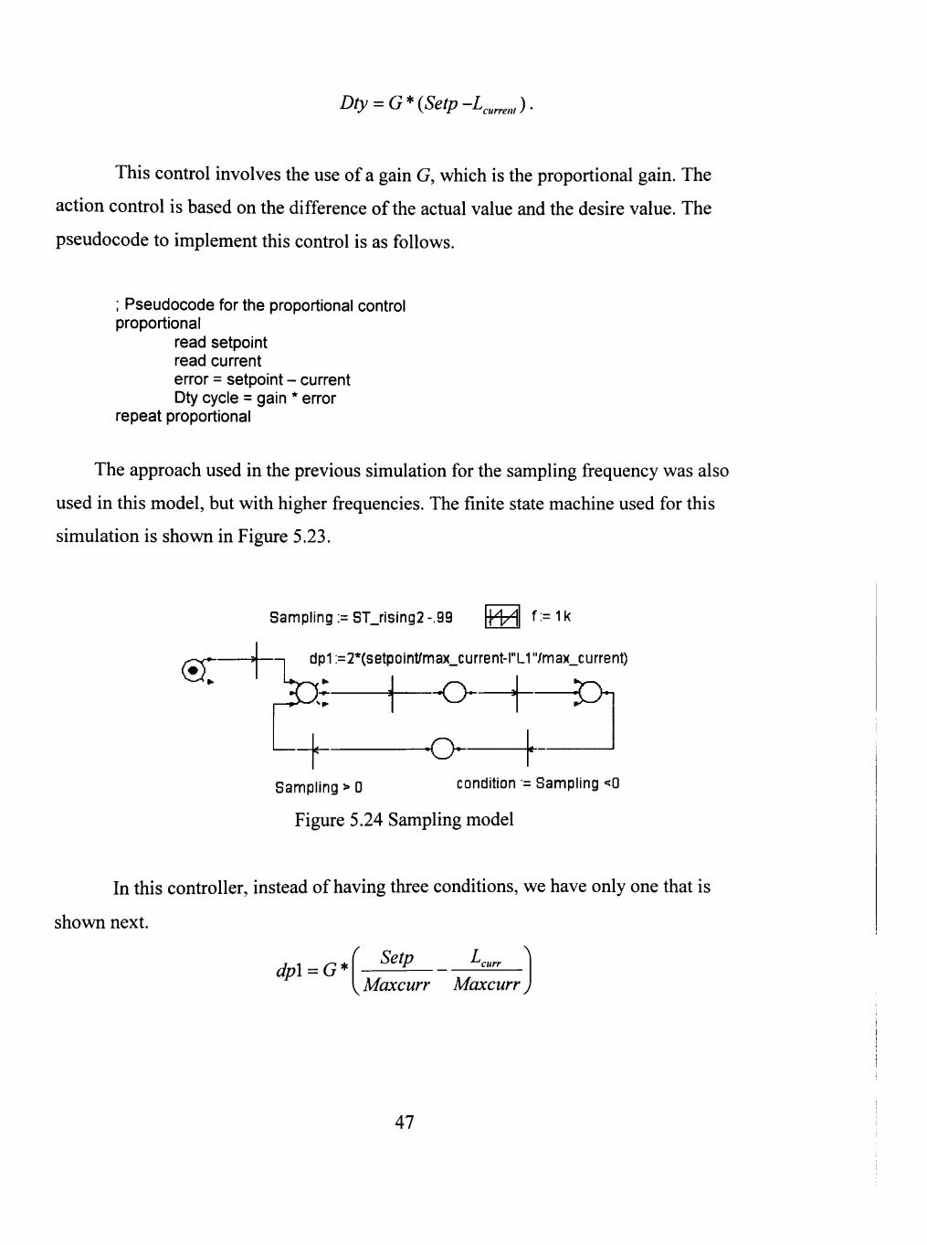
The approach used in the previous simulation for the sampling frequency was also
used in this model, but with higher frequencies. The finite state machine used for this
simulation is shown in Figure 5.23.
Sampling := ST_rising2 -.99 \A A V f : = 1 k
®: d p 1 := 2*(s etp 0 i nt/m ax_c u rre nt-1" LI 7m ax_c u rre nt)
3af O ^
o i
Sampling >0 condition - Sampling <0
Figure 5.24 Sampling model
In this controller, instead of having three conditions, we have only one that is
shown next.
^ Setp L...,, \ dpl = G - n* curr
Maxcurr Maxcurr
47
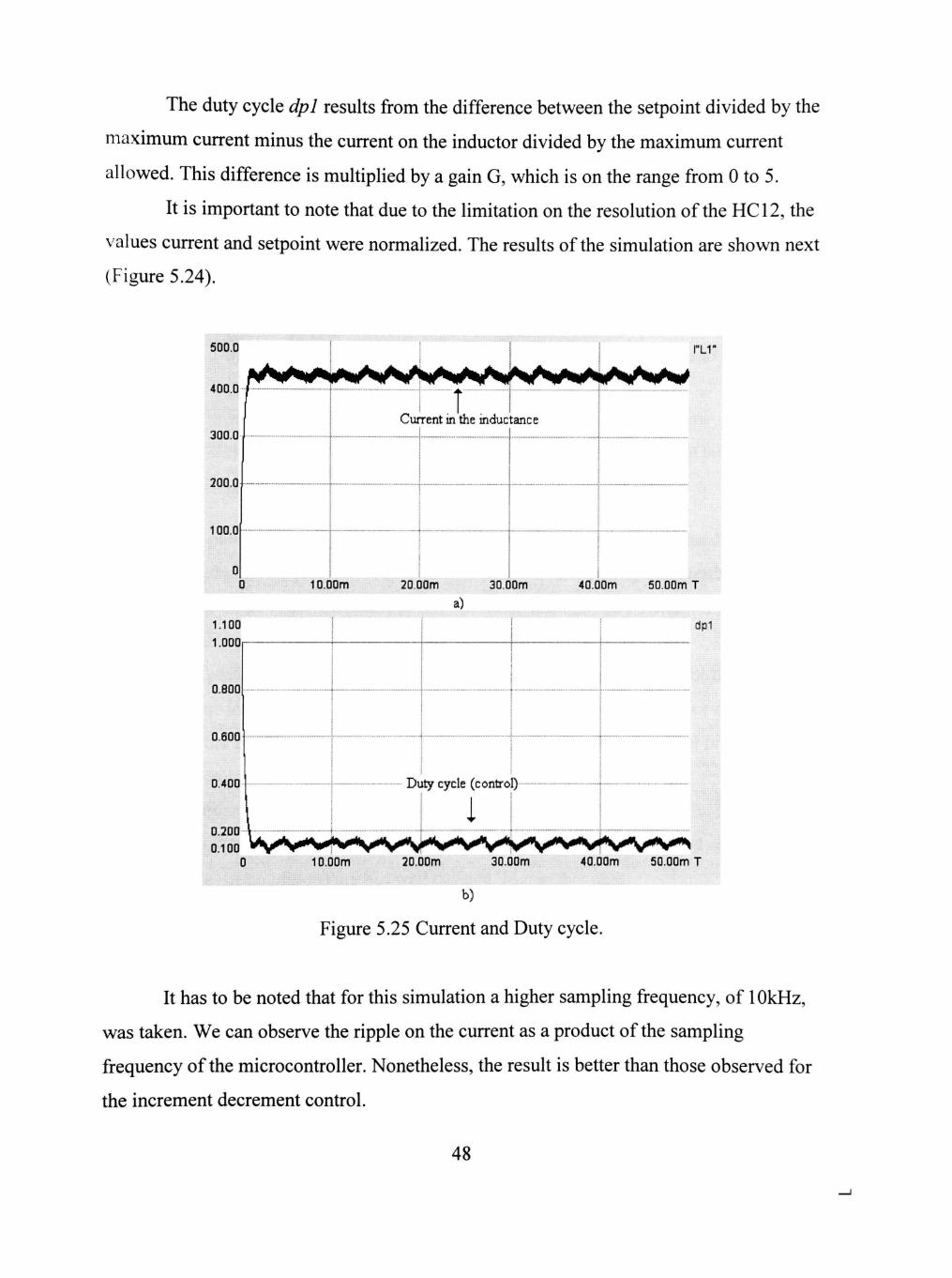
The duty cycle dpi results from the difference between the setpoint divided by the
maximum current minus the current on the inductor divided by the maximum current
allowed. This difference is multiplied by a gain G, which is on the range from 0 to 5.
It is important to note that due to the limitation on the resolution ofthe HC12, the
values current and setpoint were normalized. The results ofthe simulation are shown next
(Figure 5.24).
0.800
0.600
D.4DD
40.QQm SO.OOm T
Figure 5.25 Current and Duty cycle.
It has to be noted that for this simulation a higher sampling frequency, of 1 OkHz,
was taken. We can observe the ripple on the current as a product ofthe sampling
frequency ofthe microcontroller. Nonetheless, the result is better than those observed for
the increment decrement control.
48

On this work, both cases presented noise at the input, even with the analog filters.
For that reason, an averaging filter subroutine was implemented. The basis ofthe
averaging filter is shown on the next code for the HC12.
Sensor 1 dr
Idx Idy
avgl: movb movb addd cpx bne movb movb addd
#$093e #$093f 1,X-,1,Y-1,Y,suml sumh #$0900 avg1 ADR4H,1,Y 1,Y,suml sumh
'sumh' contains the total sum
defines the first pointer second pointer
this is a loop to push the previous values on the next location
and is repeated 62 times (3Eh) the actual value is pushed on the top of the stack and added to the average
Two pointers push one stack of 32 previous values and then the actual value is
saved and added to the previous result. The result is divided by the total number of values
added. This process is done like this to have as much accuracy as possible. It is important
to note that this process add operation time to the HC12
As a partial conclusion, the HC12 do not represent a good option for the buck
converter. The low resolution ofthe AD module present a poor performance ofthe
system, and the configuration ofthe IGBTs and the inductance also present problem, that
was the reason to take another control approach.
However, it might be possible to implement the control using the fuzzy logic
module ofthe HC12, which has special instmctions. This represents a good option for
controls were the conditions are not well defined, like in this case.
5.4 Second implemented design
For the second design a new approach was developed. Instead of having the IGBTs
and the rectifier bridges in parallel, separate modules containing each one were
implemented. Figure 5.25a shows the new configuration for the power converter using
three separate modules. Figure 5.25b shows the interior of each module.
49
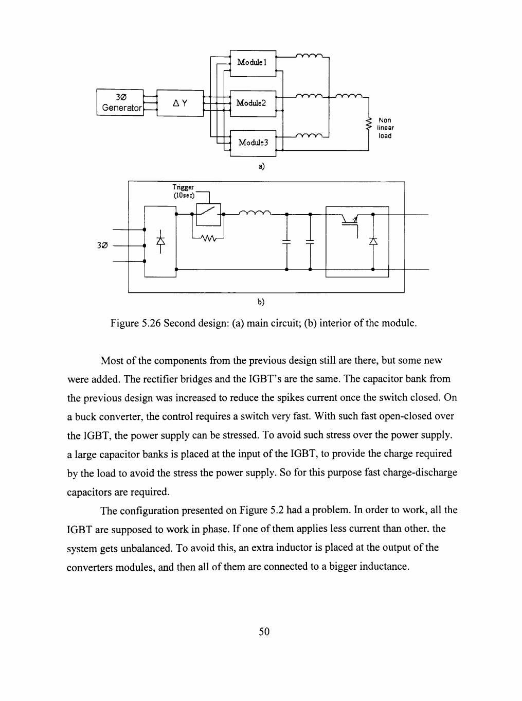
30 Generator
AY
. Module! _r> 'v>^_,
Module2
Module 3 _r>'>~v^_J
Non linear load
a)
30
Trigger (lOsec)'
i> 9-
L-Ayw-i
-f • Y^r^ zx
b)
Figure 5.26 Second design: (a) main circuit; (b) interior ofthe module.
Most ofthe components fi-om the previous design still are there, but some new
were added. The rectifier bridges and the IGBT's are the same. The capacitor bank from
the previous design was increased to reduce the spikes current once the switch closed. On
a buck converter, the control requires a switch very fast. With such fast open-closed over
the IGBT, the power supply can be stressed. To avoid such stress over the power supply,
a large capacitor banks is placed at the input ofthe IGBT, to provide the charge required
by the load to avoid the stress the power supply. So for this purpose fast charge-discharge
capacitors are required.
The configuration presented on Figure 5.2 had a problem. In order to work, all the
IGBT are supposed to work in phase. If one of them applies less current than other, the
system gets unbalanced. To avoid this, an extra inductor is placed at the output ofthe
converters modules, and then all of them are connected to a bigger inductance.
50

The second design also required another approach for the control. This involves
the design and constmction of a new board. The description ofthe control will be
explained on the section 5.4.2.
5.4.1 Interface board
For the second design, a new board was designed with different purpose. In the
previous design, the HC12 was the controller ofthe IGBTs, and the boards were designed
to assist it on that work. Now, a controller board specifically designed for that purpose
does the PWM control. Dr. Jim Dickens designed the controller circuit, which also has a
multiplexer to monitor parameters from the IGBT modules. The schematic so as the
board designed for that purpose is shown on the appendix on Figure C.13.
For this reason, the new functions ofthe HC12 are to display and to serve as an
interface between the user and the controller. The uses for the HC12 are to use a LCD, a
keyboard, to monitor analogical inputs from the controller board and to monitor error
signals from the IGBTs. The model ofthe interface between the HC12 and the modules is
show on Figure 5.26.
LCD
68HC12 Interface
board Controller
board
Keyboard
Table 5.27 Second interface
Most ofthe ports used are for general purposes, even though some of them have
an specific purpose, like the ATD or the PWM. The ports used are defined on Table 5.3.
51
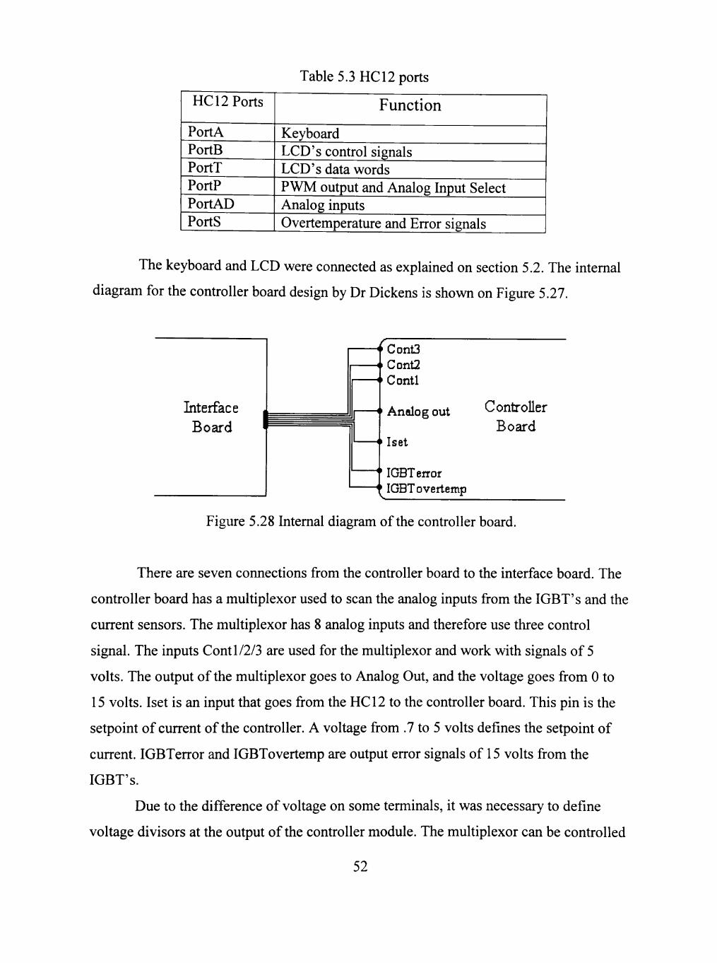
HC 12 Ports
PortA PortB PortT PortP PortAD Ports
Table 5.3 HC 12 ports
Function
Keyboard LCD's control signals LCD's data words PWM output and Analog hiput Select Analog inputs Overtemperature and Error signals
The keyboard and LCD were connected as explained on section 5.2. The intemal
diagram for the controller board design by Dr Dickens is shown on Figure 5.27.
Interface . "D .n..n..u-jj II
lioaro '
<
1 i
1 i
— — H
1 f^ l-nrti'2
' uonu > Cont2 ' Contl
» Analog out
> Iset
' IGBT error ^ IGBTovertemp
Controller Board
Figure 5.28 Intemal diagram ofthe controller board.
There are seven connections from the controller board to the interface board. The
controller board has a multiplexor used to scan the analog inputs from the IGBT's and the
current sensors. The multiplexor has 8 analog inputs and therefore use three control
signal. The inputs Contl/2/3 are used for the multiplexor and work with signals of 5
volts. The output ofthe multiplexor goes to Analog Out, and the voltage goes from 0 to
15 volts. Iset is an input that goes from the HC12 to the controller board. This pin is the
setpoint of current ofthe controller. A voltage from .7 to 5 volts defines the setpoint of
current. IGBTerror and IGBTovertemp are output error signals of 15 volts from the
IGBT's.
Due to the difference of voltage on some terminals, it was necessary to define
voltage divisors at the output ofthe controller module. The multiplexor can be controlled
52

with inputs of 5 volts, so the connection was straight. The IGBT error signals were
connected through a voltage divisor to low the voltage from 15 to 5 volts. The analog
output was also connected to a divisor since the output voltage ofthe signals varies from
0 to 15 volts. The divisor factor was of 3. Due to the configuration ofthe current sensors,
this represents a problem. The current sensors were configured for a maximum output
current of 200 mA on a resistance of 25 ohms. The divisor at the output reduces this
voltage level even more thus reducing the resolution ofthe sensors. For the setpoint the
PWM module from the HC12 was used as a digital to analog converter. For this purpose
a low pass filter was connected to the output ofthe PWM channels. The configuration for
the connections with the modules is shown on Figure 5.28.
PAD4 o-
R10 2k
IGfllCl
RO Ik
PPD o—^VA^ Ik
\fss o ppe o-PP5 o-PP4 O-
,„P' IGBTerrorl o-IGBTovtl O-
D a D • D D D • • a a D
Figure 5.29 Controller module interface.
Because more than one module was used, 4 different input-output connections
were implemented on the same board. The design ofthe board is shown in the appendix
Figure E.9.
Based on the last hardware, the new fijnction ofthe HC12 was to be a setpoint
controller. The user have to define the setpoint of each module and type of control, either
power or current. There were two basic options for the controller:
a. Current or power control,
b. Different setpoint for each module.
Likewise, the HC12 also display information on the LCD. Among the output data
are:
a. Input current,
b. Output current,
53

c. Duty cycle of the PWM controller,
d. Warning signals of over current and over voltage,
e. Output power,
f. Output voltage.
The multiplexer used was the CD4051B from T. I. As explained before, the
selection ofthe channel depend of three bits, contl, cont2 and cont3. The inputs and the
selection word from the multiplexer are listed on the Table 5.4.
Table 5.4 Multiplexer outputs
Name
^outmon
IGBT Uon
l-'mon
IGBT temp
Mnmon
Device
CLN-1000
S K i i P 1442 , lanalogOUI
UC1823A, duty cycle
SKiiP 1442, TempanaiogouT
CLN-300
Voltage range (V)
0-5
0-10
0-15
0-9
0-5
Cont 1/2/3
000
001
010
Oil
100
As previously said, the port S is used for the error and over temperature signals
from the IGBT's. As long as the new controller chip use a voltage for the current
setpoint, the HC12 use the PWM module to generate a dc output voltage using a low pass
filter. It is important to note that different setpoins were programmed in order to avoid
overcurrent on the modules if one ofthe IGBT failed. An universal setpoint could lead to
malfiinctions in the different modules.
5.4.2 Control approach
For the second design the control approach change. Due to the limitation ofthe
HC12 as the controller ofthe modules, an independent analogical controller was used, the
UC1823A from Unitrode Products. Even though two control approaches were simulated,
only one configuration for the controller was used. The controller can be configured as
voltage control and current control. Even though the configuration on the chip was set as
54
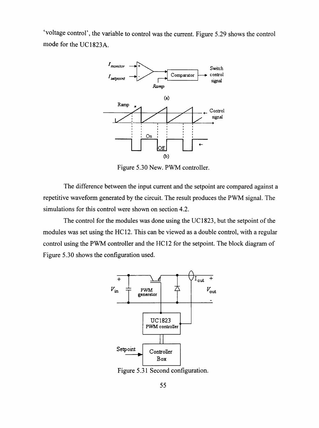
'voltage control', the variable to control was the current. Figure 5.29 shows the control
mode for the UC1823 A.
monitor
ieipoint
Switch » control
signal Ramp
(a) Ramp
Control
(b)
Figure 5.30 New. PWM controller.
The difference between the input current and the setpoint are compared against a
repetitive waveform generated by the circuit. The result produces the PWM signal. The
simulations for this control were shown on section 4.2.
The control for the modules was done using the UC1823, but the setpoint ofthe
modules was set using the HC12. This can be viewed as a double control, with a regular
control using the PWM controller and the HC12 for the setpoint. The block diagram of
Figure 5.30 shows the configuration used.
-1-
i
\J. - PWM
generator
1
Setpoint
1
UCl PWMc
Conb
2
«
>
823 ontroUei
roller Box
, (
yiout
1
-f-
f^ul
Figure 5.31 Second configuration.
55
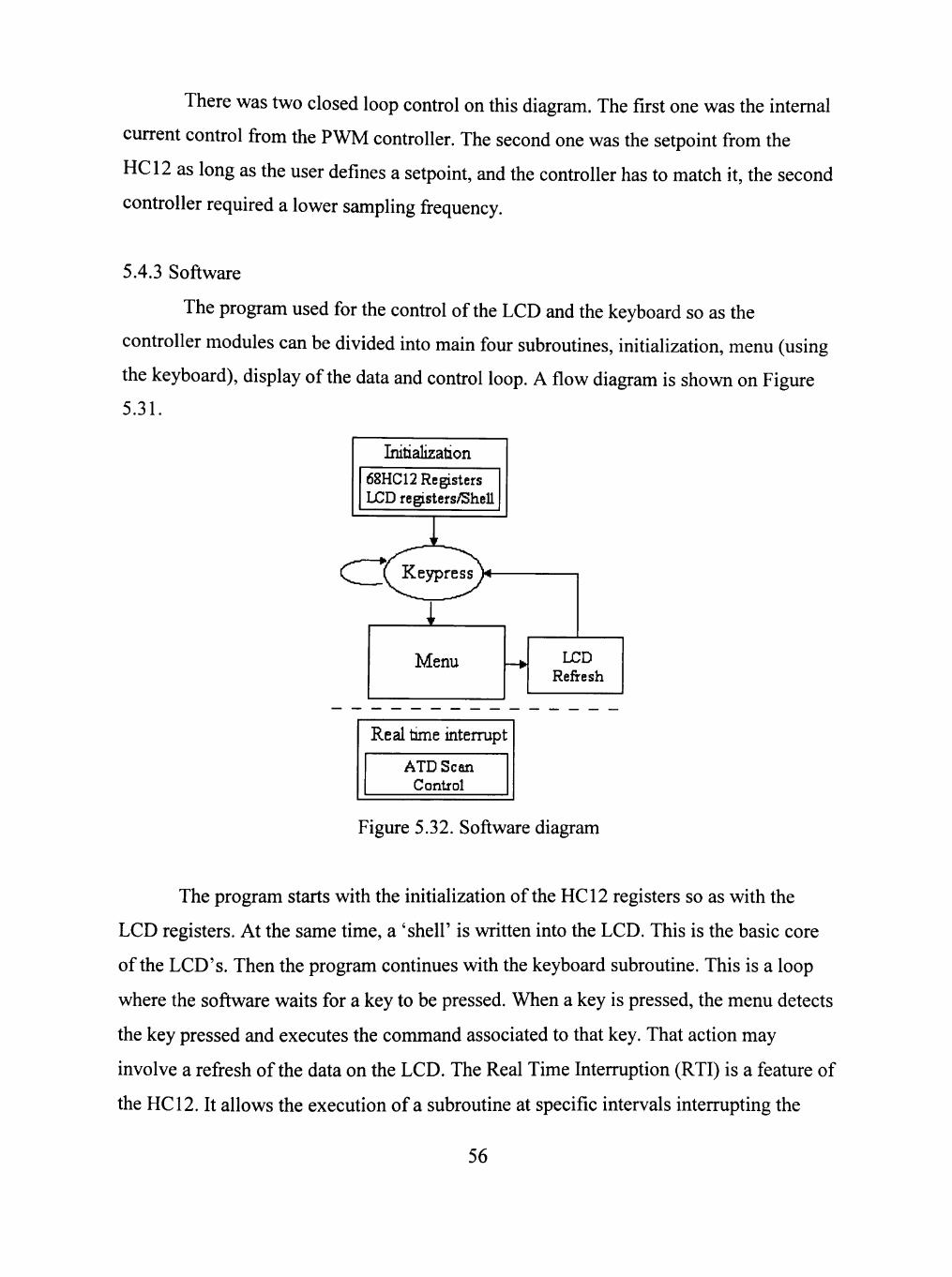
There was two closed loop control on this diagram. The first one was the intemal
current control from the PWM controller. The second one was the setpoint from the
HC12 as long as the user defines a setpoint, and the controller has to match it, the second
controller required a lower sampling frequency.
5.4.3 Software
The program used for the control ofthe LCD and the keyboard so as the
controller modules can be divided into main four subroufines, initialization, menu (using
the keyboard), display ofthe data and control loop. A flow diagram is shown on Figure
5.31.
Initialization 68HC12 Registers LCD registers/Shell
( KeypressjK
Real time interrupt
ATD Scan Control
Figure 5.32. Software diagram
The program starts with the initialization ofthe HC12 registers so as with the
LCD registers. At the same time, a 'shell' is written into the LCD. This is the basic core
ofthe LCD's. Then the program continues with the keyboard subroutine. This is a loop
where the software waits for a key to be pressed. When a key is pressed, the menu detects
the key pressed and executes the command associated to that key. That action may
involve a refresh ofthe data on the LCD. The Real Time Intermption (RTI) is a feature of
the HC12. It allows the execution of a subroutine at specific intervals intermpting the
56
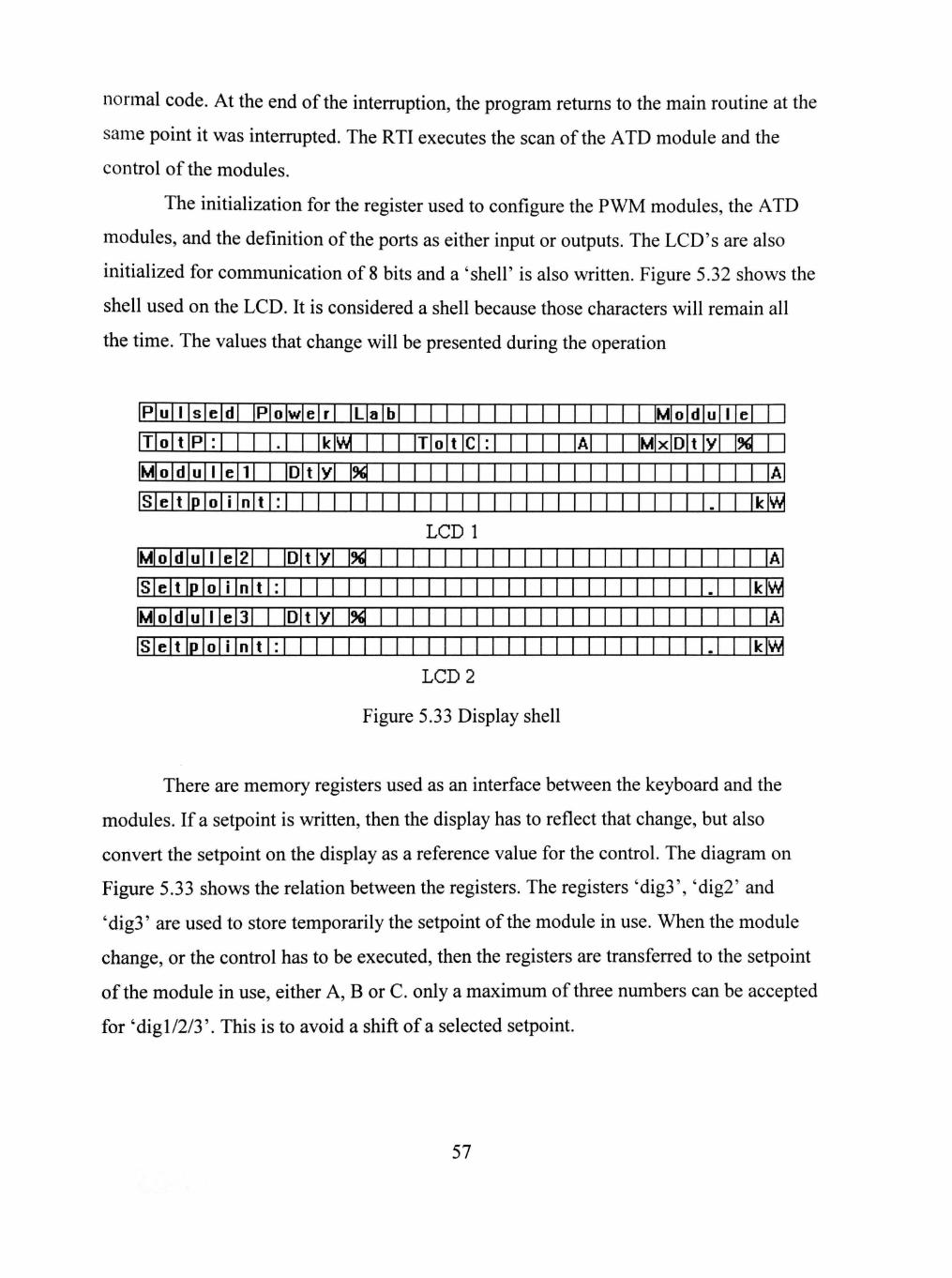
normal code. At the end ofthe intermption, the program returns to the main routine at the
same point it was intermpted. The RTI executes the scan ofthe ATD module and the
control ofthe modules.
The initialization for the register used to configure the PWM modules, the ATD
modules, and the definition ofthe ports as either input or outputs. The LCD's are also
initialized for communication of 8 bits and a 'shell' is also written. Figure 5.32 shows the
shell used on the LCD. It is considered a shell because those characters will remain all
the time. The values that change will be presented during the operation
P u l s e d P o w e r L a b M o d u l e
T o t P : kW T o t C : A M x D t y %
M o d u l e 1 D t y % A
S e t p o i n t : . k W
LCD 1
M o d u l e 2 D t y % A
S e t £.0 i n t : . k W
M o d u l e 3 D t y 9 < i A
S e t p o i n t : . k W
LCD 2
Figure 5.33 Display shell
There are memory registers used as an interface between the keyboard and the
modules. If a setpoint is written, then the display has to reflect that change, but also
convert the setpoint on the display as a reference value for the control. The diagram on
Figure 5.33 shows the relation between the registers. The registers 'dig3', 'dig2' and
'dig3' are used to store temporarily the setpoint ofthe module in use. When the module
change, or the control has to be executed, then the registers are transferred to the setpoint
ofthe module in use, either A, B or C. only a maximum of three numbers can be accepted
for 'dig 1/2/3'. This is to avoid a shift of a selected setpoint.
57

r Display
digBG) dig2(l) digl (1)
setdigA (3) setdigB (3) setdigC (3)
r
0-100% O^FFFF _
SetpointA (2) SetpointB (2) SetpointC (2)
Figure 5.34 Registers relations.
For the menu, the keyboard is used. The keyboard has 16 keys, from which 10 are
used for number codes. The character keys A, B, C, D, and # were used as commands.
Table 5.5 shows the use for each key.
Table 5.5 Keys function.
Key character
A
B
C
D
#
Function
Go. Starts the PWM
Stop. Stops the PWM
Clear. Clear the setpoint
Mode. Control selection
Module selection. Controller module selection
Description
a) Convert setdigA/B/C on setpoint values (0-100%)
b) Tum PWM on (those alowed c) Clear counter a) Decrement all duty cycles at
the same time b) Turn off the PWM a) Clear dig 1/2/3 and the counter b) Leaves same setpoints c) Reflects changes on the LCD's a) Toggle B4 of the mword (0
power/1 current) b) Clear all setdig 1/2/3 c) Reflects changes on the LCD's
a) Increment the content of modulew, changing from l->2->3 and again.
Most ofthe commands call a subroutine to display the change on the LCD's.
Figure5.34 shows the LCD's for the power and current mode.
M o d u l e D t y % 0 0 0 0 0 A
S e t ^ ^ o i n t : 0 0 . 0| |k|W P o w e r O O . O k W
a) Power mode
M o d u l e D t y %|0|0 0 0 0 A
S e t p o i n t : O O l O l l A C u r r e n t 0 0 . 0 kW
b) Current mode Figure 5.35. Display view: (a) Power mode and (b) Current mode.
58
The display of constants values was done using a subroutine inserted into the
keyboard scan. The display ofthe current, voltage, duty cycle from the controller
modules and the error signals was done in sequence. On the first loop, the value ofthe
current was displayed, on the second the voltage and so on. This was done to avoid
excessive time in the display of all the values. The limit to display each character on a
fixed time it may be a problem if numerous characters has to be displayed.
The control for the modules depends on two different subroutines, one to scan the
values ofthe ATD port and the other to control the modules based on the setpoint and the
actual value, either power or current.
The setpoint ofthe user was converted onto a normalized number o 0 to 1, or a
number for 0 to 65535, independently ofthe control mode (power or current). The control
mode then calculated the power ofthe module based on two parameters, the output
current and the duty cycle ofthe controller module. As long as the input voltage is
constant (-630V) and the output voltage depends on the duty cycle, we can calculate the
instantaneous voltage output. By multiplying the output voltage times the current, we
obtain the power. The power has to be normalized also on fractional values. For the
current applies the same. The output current is taken directly and then normalized.
Once we have the power and the current, we call the control routine. This concept
is the same as applied for the increment-decrement control ofthe last approach, but now
the PWM output is converted into a Dc signal that is used as the setpoint for the
controller module. The frequency ofthe control is IkHz, so the reference is almost
constant. The control is before. The setpoint is compared against the reference ofthe user
(power or current) and according to the actual value the duty cyclke in incremented or
decremented to adjust the values.
It can be considered that this control can be risky if we consider there are two
feedbacks for the same purpose.
59

CHAPTER 6
CONCLUSIONS
The objective ofthe project was to control up to lOOkWatts. Practical test on field
shows that it is possible to melt the soil with more that 50kWatts.
The first design implemented to control the power converters present problems.
The low resolution ofthe ATD converter on the 68HC12, the resolution on the PWM, the
configuration ofthe IGBTs and the inductance and the low capacitors at the input causes
instability on the control using the 68HC12. One option could be the use ofthe fiizzy
control module on the 68HC12.
The second design was more stable for different reasons. The control with the
UCl823A was stable and very precise. To split the IGBTs, rectifier bridges and
capacitances into separate modules proves to be a good option to protect the modules
from each other.
The 68HC12 shows as a good option to interface the user with LCD and
keyboard. Nonetheless the microcontroller was instable on the field due to the electric
noise.
With more time, fiirther improvements can be made to ensure a correct interface
between the mutiplexer and the 68HC12. The simulations also show that it is
recommended that the inductances at the output ofthe modules are equal and also the
setpoints ofthe modules.
60

REFERENCES
1. Mohan, Ned. Power Electronics. John Wiley & Sons, New York, 1995.
2. Bayne, B. Stephen. High Power Semiconductor Switching and Reliability, Thesis, Texas Tech University, Dec. 1994.
3. Benda, Vitezslav. Power Semiconductor Devices. John Wiley & Sons, New York, 1994.
4. Blicher, Adolph. Thvristor Physics. Springer-Verlag,New York, 1976.
5. Cogdell, J.R. Foundations of Electrical Engineering. Prentice Hall, Inc., Englewood Cliffs, NJ, 1996.
6. Laster, Clay. Thvristor Theory and Application. Tab Books Inc., Blue Ridge Summit, PA, 1986.
7. Portnoy, W.M. "Thyristors as Switching Elements for Pulsed Power," Pulsed Power Lecture Series, Lecture no. 23. 1980.
8. Streetman, Ben G. Solid State Electronic Devices. Prentice Hall Series in Solid State Physical Electronics, Upper Saddle River, New Jersey, 2000.
9. Motorola Semiconductor. Technical Data MC68HC912B32. Motorola INC. 1997
10. Spasov, Peter. Microcontroller Technology. Regent/Prentice Hall. Englewood Cliffs, NJ. 1993
11. Motorola. Evaluation Board, M68EVB912B32 User's Manual. Motorola INC. 1997
12. Motorola. 68HC12 Reference Manual. Motorola INC. 1997
13. Lipovski, Jack G. Microcontroller interfacing. Academic Press. San Diego, CA. 1999
61

APPENDIX A
68HC12 CODE
62
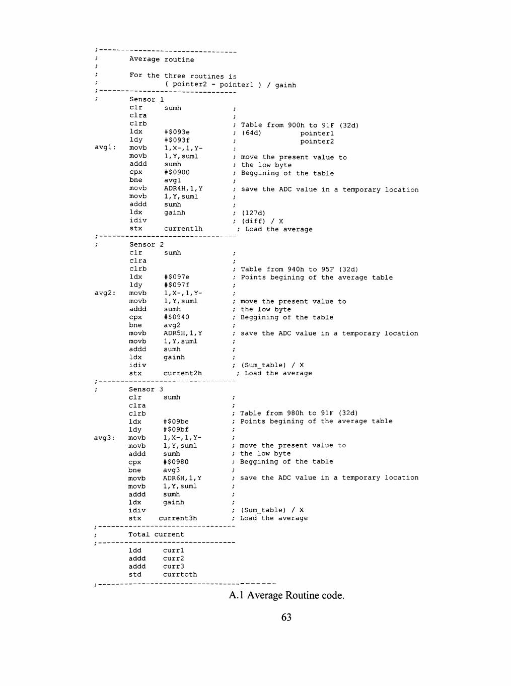
avgl
avg2 :
avg3 :
Average routine
For the three routines is ( pointer2 - pointerl ) / gainh
Sensor clr clra clrb Idx Idy movb movb addd cpx bne movb movb addd Idx idiv stx
sumh
#$093e #$093f 1,X-,1,Y-1, Y, suml sumh #$0900 avgl ADR4H,1,Y 1,Y,suml sumh gainh
currentlh
Sensor clr clra clrb Idx Idy movb movb addd cpx bne movb movb addd Idx idiv stx
sumh
#$097e #$097f 1,X-,1,Y-1, Y,suml sumh #$0940 avg2 ADR5H,1,Y 1,Y,suml sumh gainh
current2h
Sensor clr clra clrb Idx Idy movb movb addd cpx bne movb movb addd Idx idiv stx
sumh
#$09be #$09bf 1,X-,1,Y-1,Y,suml sumh #$0980 avg3 ADR6H,1,Y 1, Y, suml sumh gainh
current3h
Total current
Idd addd addd std
currl curr2 curr3 currtoth
Table from 900h to 91F (32d) (64d) pointerl
pointer2
move the present value to the low byte Beggining of the table
save the ADC value in a temporary location
(127d) (diff) / X
; Load the average
Table from 940h to 95F {32d) Points begining of the average table
move the present value to the low byte Beggining of the table
save the ADC value in a temporary location
(Sum_table) / X ; Load the average
Table from 980h to 91F (32d) Points begining of the average table
move the present value to the low byte Beggining of the table
save the ADC value in a temporary location
(Sum_table) / X Load the average
A. 1 Average Routine code.
63

* MAIN PROGRAM
loop:
Idaa ADR2H ; A -> analogical input staa set_pointl ; A = Setpoint
proport
Idab stab sba bcs Idab mul staa exg Idaa Idy emul cpd bcc stab stab
ional control
ADR4H currentlh ;
end #$C8
error ; A,B #$00 #$0001
#$00C7 end ; PWDTYO PWDTYl
B = Currentl A - B -> A, error = Set-Curr if negative, go to end to adjust the duty cicle to C8h (lOkHz)
Y = Proportional Gain
if not,
end:
bl
Sampling frequency
Idx #$003F dex bne bl
Delay for a sample frequency of Ifh = 20kHz OOh 80kHz
A.2 Proportional control code.
64

APPENDIX B
SIMULATIONS
65
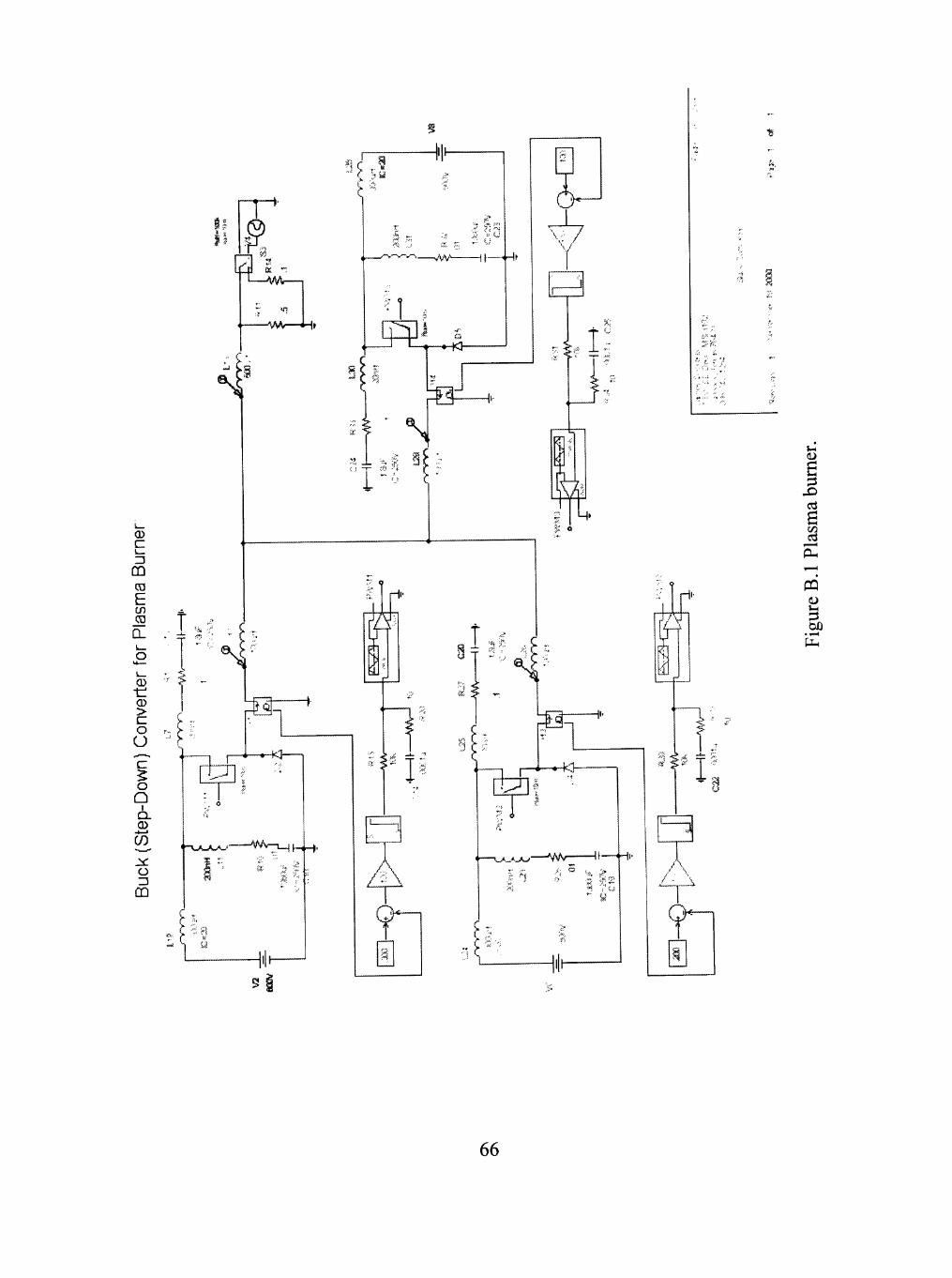
c Zi
m
E en D_
CD
> C o O 'E' o Q
I Q.
o Z3
[^
I ^ ^ 1
-VVA,^-H»
%
w -k1—I
' '-VA.A.A^ ^^^CM H H'
•^ r ^^^
* -
i j i i Ii
T
< j
Zi-^~
4c^
U..*_AJO *^W-
Hil^
'*• •;?,
Ml-
/v
m
" ^ : -
1 s * I
/ • \
o
i
• 1-H
66
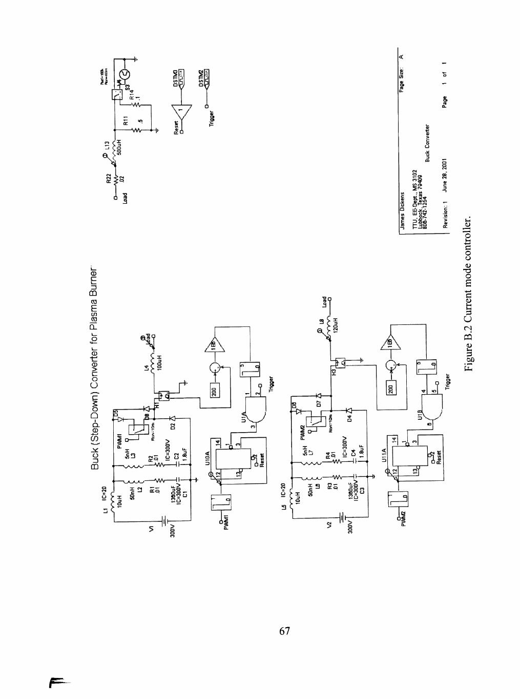
I 01
0) > c o u
«20B
- M
H.X-* aTvo
t=3g > (V
i _
m TO
E
CL
0)
> c o O
5 o Q
I
Q. © -t—'
CO J^ o rs
CD
^ J ' . " do
c
O
—vi/v—I *—H' ? 3 £5 =1
:2o
H Ii
O o
o
U
OX)
67

APPENDIX C
CONTROLLER BOARDS
68
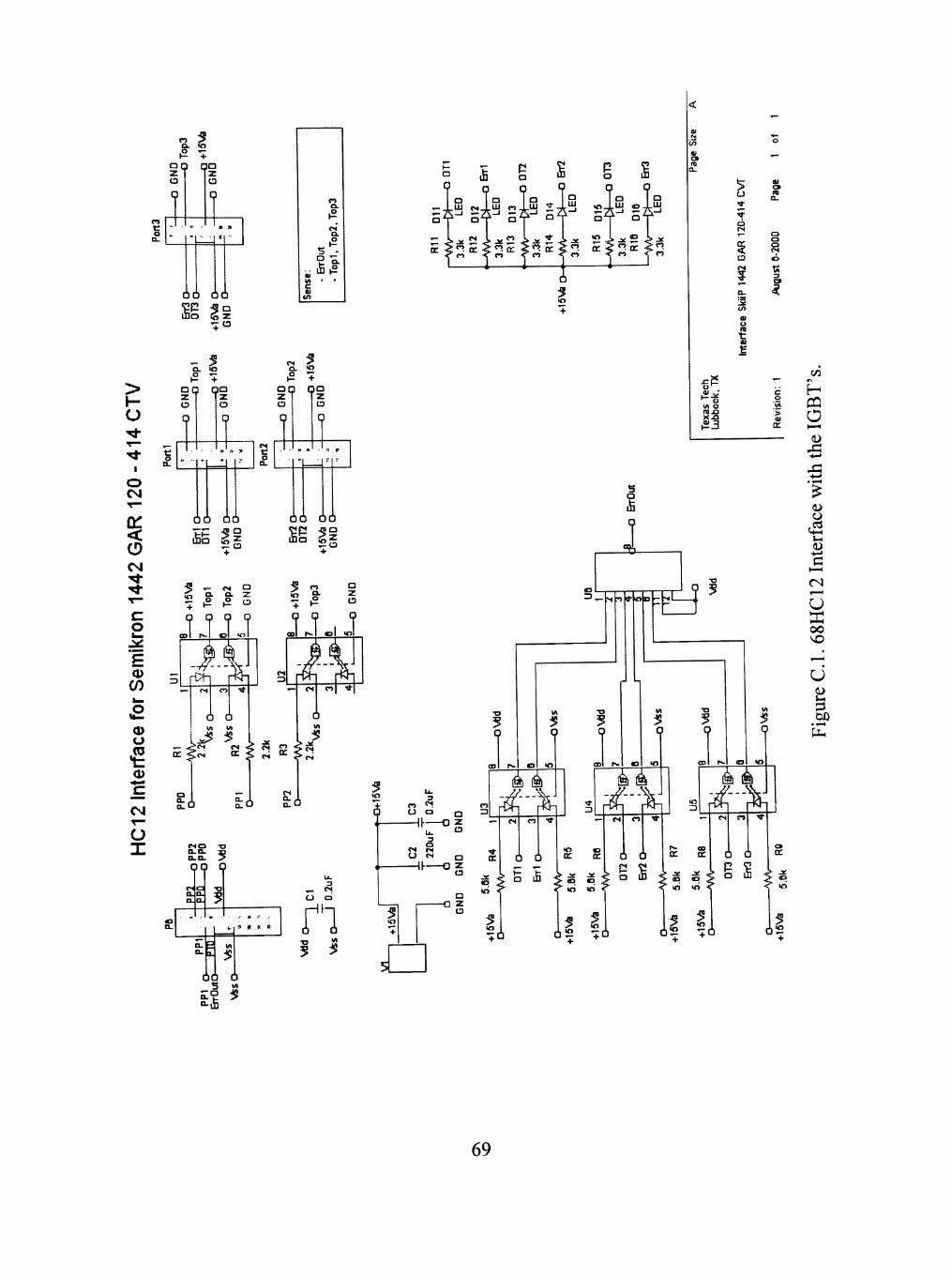
> I -u
o CM
<
CM
C
o
0)
0)
CM
O
c 2 U c
y
3
p
t
)
,
)t
c
)
z c c
c
) J
IC
•M
1
LDO io z
^ ?
O Q Z
o Q
Q Q Z o
CN Q.
• g z o 0
3 '+
z u Q
do DO
mo
do d d 5 1 +
s p 5 0
a I • l a
s p o
U^ si^S: o
ra
t
OI
ra a .
a o OH
o
• ^ o VI o ni.a
i23
s a
JSi.
^ • . - N r» »• o D
•o
Q
00 r^ o m
FFy
5 a 0
O-O. s 0 . 0 . ?
QQ Q
i, s ti k 9
dd d 5:° S n-lS
O d
-o
5 Q
CO r^ 0 t?
Q
^...XXi
( ,
5
3
II
u.
c 1 II - 0
O
• CE Z u
r^i
d d
^ ^ 5 S
cp r^ <g f?
5 Q
IT K
jS3 c
A 6
O 111
4 i
(E K d d a 111
3 1(3
3 Q ^ : ;
on
H O
o < 4 - l
U 00
U
GO • 1-H
69
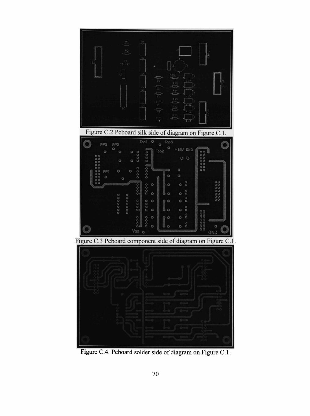
Figure C.2 Pcboard silk side of diagram on Figure C. 1
Figure C.3 Pcboard component side of diagram on Figure C.l,
Figure C.4. Pcboard solder side of diagram on Figure C.l
70
u <v
<— p o
I -0)
o
(/)
I k . o w c o
CO CM
o
ID a z u
5
V) o ra ^
.23
TT
d d
^ o> ^
+
4 C
T TT
o d d
i <S s +
5 3 •O IO
ITT
g i Q Q 4
v._
d d
« ^ ^ +
o t - l
c3 ••->
. l - H
• 1-H
O
o o
a
yr\
U >-i :3 &o
• ^H
71
Figure C.6 Pcboard silk side of diagram on Figure C.5.
Figure C.7 Pcboard component side of diagram on Figure C.5.
Figure C.8 Pcboard solder side of diagram on Figure C.5.
72
e
CD cn
i2
CM
u X CO ( O i— 0)
o u X o
CD
O o O o O o O o
O-
IF
<-iD
w cr
nmm\ iopi-vvv—ii
- Tl>n-a-r ' r j i t j n.Q.Q.
n OOOOCpOOO
</>(/)(/> en 0 . 0 . 0 . 0 .
a - . - M r * * • ! «
0 . 0 . 0 . 0 . 0 . 0 .
dddddddddd (DO) I— I—f- Dl— O. O.O. 0 . 0 . 0 . ^ 1 ^ ^ ^ 0 - 0 - 0 .
c
c
* 1
1
p c
•• P 9> 0 ff
(
pc
.
IC
pc
-
I t
pc
l.
IC
p
.
1
^o—1..
o o . Q.
r - i o r j " -O-O-O-O.
< m < a ]
Q - i - M O ^ l O O ^ -^D ^D CD^D CD ^D^D CD
• o a o a a a o
o * N a > n n ffiCD ^
o a a o K qp CD
—VVVpi'
I S - m o — _. • ' S r a
5S < O- a . D . D . > £ £
\os-^AA—|i
— j N r j ' ^ i o P H P P c
c
p
-
K
c
« •
J
pc
c
p c
' 9 W '
C 9 It W
1 c
p
1
c
.
c
p(]
-
lie
pc
-
IC
[I ' • » |r » »
"- » f p «
) c
PC
»
K
p m
It
\
a a
n»o mm O-O- O- O - O - O -
(3 CDC)
T ^ O IJ
< U
m m ^ m ^
a o o a o : mn Q i l
- ^ V W i i .
5§ ddddddddc) O- O-O- O. O-O. O- O-U)
liJ a:
• a wi
illctSlll' IS. lo ry- 4u> ~ a»o mmmmQp: j j ^ a a a o '
Q U
I
a o
CN
U
o
X o
"o
o U ON
U a> i - i
73
Figure CIO Pcboard silk side of diagram on Figure C.9.
Figure C.l 2 Pcboard solder side of diagram on Figure C.9.
74
N
-*\
m
" ^ O S
C 1 I
* <-M(ovin«
o
3 1
8'* o
n n ii i
- ^ o
Sfi
/ • « — 1 °
^ \ A ^ 1>
SS
1% u o
9S
Is'
I I I
HI li-
Ss
ft^
2 Ut
6 a
3 «_ I < § > S 3 (J g ( J g Ul Z S L*)
n
HI—1>"
BS
se
H i 1>
HI 0 5 %
-P
|§ |8 j
u 4. 'Hfy.
« 3 a] q: 4 I
5 •_< = cJ__2t--H>
N
r)
o 15
o 00 ;-!
'o
O
O H
OX)
n^
£9 ll ^ « J! » T • 9 9 9
.-(sr>.r tft «
CO
75
Figure C.14 Pcboard silk side of diagram on Figure C.13
Figure C.15 Pcboard component side of diagram on Figure C.13.
Figure C.l 6 Pcboard solder side of diagram on Figure C.13.
76
Figure C.17 Controller Interface
Figure C.18 Analog Interface
77
ll->
Hi||i«itmiii.; . It \Ux.m\
I ~mipi!l!!llli!!! iiiyiiiii
Figure C.19 68HC12 General Interface
I I i
B B B B B B B B B B B B B B B B
Figure C.20 Box cover.
78

APPENDIX D
TORCH TRUCK
79
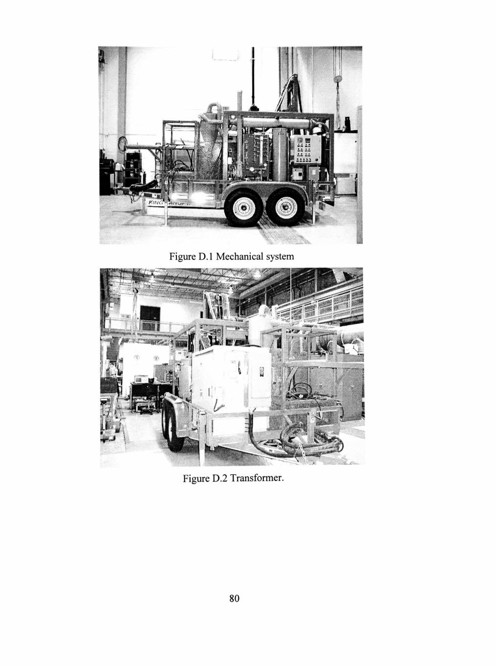
-W^mmm^
Figure D.l Mechanical system
Figure D.2 Transformer.
80
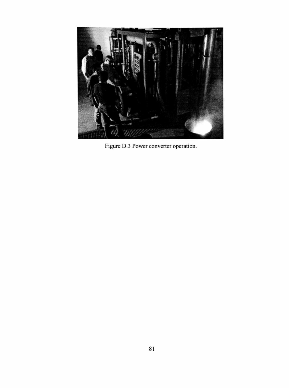
Figure D.3 Power converter operation.
81

PERMISSION TO COPY
In presentmg this thesis m partial hilfillmcnt ofthe requirements for a master's
degree at Texas Tech University or Texas Tech University Health Sciences Center, I
agree that the Library and my major department shall make it freely available for
research purposes. Permission to copy this thesis for scholarly purposes may be
granted by the Director ofthe Library or my major professor. It is understood that
any copying or publication of this thesis for financial gam shaU not be allowed
without my further written permission and that any user may be liable for copyright
infringement.
Agree (Permission is granted.)
Student Signature Date
Disagree (Permission is not granted.)
Student Signature Date