2d nanosheets as functional building blocks for 1d photonic
TRANSCRIPT
DISSERTATION ZUR ERLANGUNG DES DOKTORGRADES DER FAKULTÄT FÜR CHEMIE UND PHARMAZIE DER
LUDWIG-MAXIMILIANS-UNIVERSITÄT MÜNCHEN
2D NANOSHEETS AS FUNCTIONAL BUILDING BLOCKS
FOR 1D PHOTONIC CRYSTAL SENSORS
Katalin Szendrei-Temesi (geb. Szendrei)
aus
Budapest, Ungarn
2018


3
ERKLÄRUNG
Diese Dissertation wurde im Sinne von §7 der Promotionsordnung vom 28. November 2011 von Frau
Prof. Dr. Bettina V. Lotsch betreut.
EIDESSTATTLICHE VERSICHERUNG
Diese Dissertation wurde eigenständig und ohne unerlaubte Hilfe erarbeitet.
München, 20.06.2018
Katalin Szendrei-Temesi
Dissertation eingereicht am: 20.04.2018
Erstgutachterin: Prof. Dr. Bettina V. Lotsch
Zweitgutachter: Prof. Dr. Achim Hartschuh
Mündliche Prüfung am: 28.05.2018


5
Apukámnak
“Just because something doesn't do what you planned it to do doesn't mean it's
useless.”
Thomas Alva Edison
6
KÖSZÖNÖM! DANKE! THANK YOU!
Mein größter Dank geht an meine Doktormutter Bettina Lotsch, ohne die diese Arbeit nicht möglich
gewesen wäre. Danke für Deine fachliche Expertise, Deine Begeisterung für das Thema, für die
Freiheit beim Forschen, für die ausfühliche Korrekturrunden, für die fachlichen und weniger
fachlichen Diskussionen in guten und schlechten Zeiten, für die Konferenzreisen, die Unterstützung
bei der Bewerbung für die Preise an den Konferenzen!
Prof. Achim Hartschuh möchte ich mich für die Übernahme der Rolle des Zweitgutachters bedanken.
Bei meiner Prüfungskommission, bestehend aus Prof. Lena Daumann, Prof. Konstantin Karaghiosoff,
Prof. Hans-Christian Böttcher und Prof. Thomas Bein möchte ich mich für die Zusage und Teilnahme
an meiner Doktorprüfung und für die spannenden Diskussionen über meine Arbeit bedanken.
Alleine hätte ich diese tollen Projekte natürlich nicht geschafft, vielen Dank an die Co-Autoren und
Mitwirkenden an den unterschiedlichen „bunten“ Projekten. Mein besonderer Dank geht an
Dr. Alberto Jiménez-Solano für das optische Resonatorprojekt, das wir zusammen in Sevilla während
meines Forschungsaufenthaltes durchgeführt haben, für das Meistern der Herausforderungen im
Diffusionsprojekt, für seine Expertise in Optik und seine „magic“ in Matlab, die er mir stets versucht
weiterzugeben und natürlich für die Korrektur dieser Dissertation – ¡Muchas gracias! Weiterhin
möchte ich mich bei Dr. Gabriel Lozano und Prof. Hernán Míguez bedanken für die tolle Zeit in Sevilla
am ICMSE-CSIC und das spannende optische Resonatoren Projekt, für ihre Expertise in Optik und
Photonik – ¡Gracias! Bei Pirmin Ganter möchte ich mich für das „H3“ (touchless positioning
interfaces) und „H1“ (Photonische Nase) Projekt, für seine fachliche Expertise, für die
wissenschaftlichen Diskussionen und natürlich für die Nanosheets selber bedanken. Dr. Olalla
Sanchéz-Sobrado danke ich für ihre Unterstützung aus der Ferne bei der Veröffentlichung vom
Touchless-Projekt und für die Idee, die ersten Ergebnisse und die wissenschaftlichen Diskussionen
beim „all-nanosheet“ Projekt. Dr. Sophia Betzler danke ich für die tollen EELS Messungen im Rahmen
des „all-nanosheet“ Projektes und für ihre Begeisterung für das Thema.
Für die externe Betreuung von dieser Doktorarbeit und für die zahlreichen internen Reviews möchte
ich mich bei Dr. Hans Boschker bedanken.
Die zahlreichen wundervollen SEM cross section Bilder danke ich Viola Duppel ganz herzlich. Danke
für Deine Ausdauer mit den komplizierten, sich zusammenfaltenden Proben! Ein großer Dank geht an
Willi Hölle für den Bau der Feuchtekammern, Plexiglas Scheiben und diverse Kleingeräte.

7
Ich möchte meinen Praktikanten ganz herzlich für die spannenden Ergebnisse und Diskussionen
danken, und ich hoffe, dass ihr Spaß hattet mit meinen bunten Forschungsthemen: Bernhard Illes
danke ich für die Messungen am „H1-Selektivität“-Projekt, Andre Mähringer für das unveröffentlichte
MOF/nanosheet Bragg stack Projekt, Jakob Blahusch und Katharina Durner für das „all-nanosheet“
Projekt, Denis Hartmann und Carola Lampe für das „Transfer“ Projekt, und Dimitra
Chatzitheodoridou für das „Diffusion und Aminprojekt“.
Ich möchte mich bei dem kompletten AK Lotsch für diese schönen 3,5 Jahre bedanken, für die lustige
Zeit sowohl in München, also auch in Stuttgart. Einen besonderen Dank geht an die direkten
Münchner Kollegen für die Gruppenveranstaltungen, die wissenschaftlichen Diskussionen und für das
Zuhören in guten und in schlechten Zeiten: Albi, Kerstin, Claudi, Sascha, Anna, Leo, Charlotte,
Hendrik, Stefan, Lars, Dimitra, Annick, Verena, Natalie – Danke!
Für die organisatorische Hilfe im Laufe der Doktorarbeit möchte ich mich bei diversen Leuten ganz
herzlich bedanken – ihr habt meinen Alltag erleichtert. Vielen Dank an Claudia Kamella, die sich um
alle Stuttgarter Angelegenheiten gekümmert hat und wenn sie nicht selber helfen konnte, wusste sie
sofort, an wen man sich wenden soll und an Sigrid Fuhrmann, die sich um die Verwaltungssachen
gekümmert hat. Mein besonderes Dankeschön oder besser gesagt „Köszönöm“ geht an Olga Lorenz,
die mit den Münchner organisatorischen Angelegenheiten behilflich war. Bei Wolfgang Wünschheim
möchte ich mich für die Lösung aller IT-Probleme und bei Thomas Miller für seine technische Hilfe
bedanken.
Für das NIM (Peter Sonntag, Christoph Hohmann, Birgit Ziller, Isabella Almstätter und Silke
Mayerl-Kink) und CeNS team (Susanne Hennig, Claudia Leonhard und Marilena Pinto) möchte ich
mich neben dem „travel award“ und „research visit funding“ für die tollen Veranstaltungen für die
schöne Zeit im Student board, für die Pressemeldungen (Birgit Ziller und Isabella Almstätter) und für
das Cover Bild und für die Grundlagen im 3D image design (Christoph Hohmann) bedanken.
Köszönöm a családomnak a támogatást így a távolból is! Köszönöm, Lacinak, Attilának, Csabinak,
Dórinak és Áginak (Bros&Partners), Anyának, Mamának, Papának, Gábornak a támogatást, illetve
Apukámnak, aki ezt ugyan nem láthatja, de a matematika és a természettudományok iránti szeretét
kellő mértékben átadta, hogy idáig eljussak.
Végül, de nem utolsó sorban köszönöm férjemnek, Gábornak a támogatást és a biztatást nem csak ez
alatt a 3,5 év alatt, hanem mindig. Köszi mindenek előtt a türelmedet, a sok szeretetet, a tanácsaidat,
a mindig diplomatikus megoldási javaslatokat, illetve egyszerűen, hogy vagy.

8
TABLE OF CONTENTS
1. INTRODUCTION 15
1.1 PHOTONIC CRYSTALS 17
1.2 ONE-DIMENSIONAL PHOTONIC CRYSTALS 18
1.2.1 OPTICAL PROPERTIES OF 1D PHOTONIC CRYSTALS 18
1.2.2 OPTICAL PROPERTIES OF RESONATORS 22
1.3 OPTICAL SENSING VIA PHOTONIC CRYSTALS 23
1.3.1 FUNCTIONAL MATERIAL BASED SOLUTION PROCESSED 1D PHOTONIC CRYSTALS FOR CHEMICAL SENSING
APPLICATIONS 24
1.3.1.1 SENSING PLATFORMS BASED ON RI CHANGES – POROUS 1D PHOTONIC CRYSTALS 25
1.3.1.2 SENSING PLATFORMS BASED ON LAYER THICKNESS CHANGES 29
1.3.2 CURRENT CHALLENGES IN PHOTONIC CRYSTAL SENSING 31
1.4 2D MATERIALS 33
1.4.1 EXFOLIATION 33
1.4.2 2D MATERIALS FOR GAS AND VAPOR SENSING 35
1.5 OBJECTIVES 36
1.6 REFERENCES 38
2. METHODS 47
2.1 FABRICATION METHODS 47
2.1.1 SPIN-COATING 47
2.2 CHARACTERIZATION TECHNIQUES 49
2.2.1 ULTRAVIOLET-VISIBLE SPECTROPHOTOMETRY 49
2.2.2 MASS FLOW CONTROL OF VAPORS 51
2.2.3 SPECTROSCOPIC ELLIPSOMETRY 52
2.2.3.1 ELLIPSOMETRIC POROSIMETRY 54
2.2.4 PHOTOLUMINESCENCE 56
2.2.5 SCANNING ELECTRON MICROSCOPY 58
2.2.5.1 ENERGY DISPERSIVE X-RAY SPECTROSCOPY 60
2.2.6 TRANSMISSION ELECTRON MICROSCOPY 61
2.2.6.1 ELECTRON ENERGY LOSS SPECTROSCOPY 63
2.2.7 X-RAY DIFFRACTION 65
2.2.8 DYNAMIC LIGHT SCATTERING 66
9
2.2.9 ATOMIC FORCE MICROSCOPY 67
2.2.10 IMPEDANCE SPECTROSCOPY 68
2.3 THEORETICAL CALCULATIONS 68
2.3.1 TRANSFER MATRIX METHOD 69
2.3.2 GENETIC ALGORITHMS 71
2.4 REFERENCES 73
3. NOVEL SENSING APPLICATIONS ENABLED THROUGH ULTRAHIGH HUMIDITY SENSITIVITY: AN
OPTICAL TOUCHLESS POSITIONING INTERFACE 77
3.1 SUMMARY 77
3.2 TOUCHLESS OPTICAL FINGER MOTION TRACKING BASED ON 2D NANOSHEETS WITH GIANT MOISTURE
RESPONSIVENESS 79
3.3 INTRODUCTION 79
3.4 RESULTS AND DISCUSSION 80
3.5 ACKNOWLEDGEMENTS 91
3.6 REFERENCES 92
4. PRACTICAL ASPECTS OF THE OPTICAL TOUCHLESS POSITIONING INTERFACE: SELECTIVITY,
REPRODUCIBILITY, TEMPERATURE DEPENDENCY 95
4.1 SUMMARY 95
4.2 TESTING THE SELECTIVITY, CYCLING STABILTY AND THE TEMPERATURE DEPENDENCY OF TOUCHLESS
FINGER MOTION TRACKING DEVICES BASED ON 1D PHOTONIC CRYSTALS 97
4.3 ABSTRACT 97
4.4 INTRODUCTION 98
4.5 RESULTS AND DISCUSSION 99
4.6 EXPERIMENTAL 107
4.7 REFERENCES 109
5. TAILORING THE SENSOR`S SELECTIVITY: OPTICAL DISCRIMINATION OF DIFFERENT SOLVENTS
BY 2D NANOSHEET BASED 1D PHOTONIC CRYSTALS 111
5.1 SUMMARY 111
5.2 TOWARDS THE NANOSHEET-BASED PHOTONIC NOSE: VAPOR RECOGNITION AND TRACE WATER SENSING
WITH ANTIMONY PHOSPHATE THIN FILM DEVICES 113
5.3 INTRODUCTION 113
5.4 RESULTS AND DISCUSSION 114

10
5.5 ACKNOWLEDGEMENTS 125
5.6 REFERENCES 125
6. OPTIMIZING THE OPTICAL PROPERTIES: LITHIUM TIN SULFIDE NANOSHEET BASED 1D
PHOTONIC CRYSTALS 127
6.1 SUMMARY 127
6.2 LITHIUM TIN SULFIDE – A HIGH-REFRACTIVE-INDEX 2D MATERIAL FOR HUMIDITY-RESPONSIVE PHOTONIC
CRYSTALS 129
6.3 ABSTRACT 129
6.4 INTRODUCTION 129
6.5 RESULTS AND DISCUSSION 131
6.6 EXPERIMENTAL SECTION 143
6.7 ACKNOWLEDGEMENTS 145
6.8 REFERENCES 146
7. TOWARDS ALTERNATIVE READOUT SCHEMES: FLUORESCENT HUMIDITY SENSORS BASED ON
OPTICAL RESONATORS 149
7.1 SUMMARY 149
7.2 FLUORESCENT HUMIDITY SENSORS BASED ON PHOTONIC RESONATORS 151
7.3 ABSTRACT 151
7.4 INTRODUCTION 151
7.5 RESULTS AND DISCUSSION 153
7.6 EXPERIMENTAL SECTION 161
7.7 ACKNOWLEDGEMENTS 163
7.8 REFERENCES 163
8. TRACKING THE SENSING MECHANISM: DIFFUSION TRACKING OF VAPOR ANALYTES IN
MULTILAYERED STRUCTURES 167
8.1 SUMMARY 167
8.2 TRACKING VERTICAL MOLECULAR DIFFUSION INTO 1-DIMENSIONAL PHOTONIC CRYSTALS 169
8.3 ABSTRACT 169
8.4 INTRODUCTION 169
8.5 RESULTS AND DISCUSSION 171
8.6 ACKNOWLEDGEMENTS 178
8.7 REFERENCES 178

11
9. CONCLUSION AND OUTLOOK 181
9.1 OUTLOOK 183
9.2 REFERENCES 185
10. APPENDIX 187
LIST OF ABBREVIATIONS 188
10.1 SUPPORTING INFORMATION FOR CHAPTER 3 190
10.2 SUPPORTING INFORMATION FOR CHAPTER 5 209
10.3 SUPPORTING INFORMATION FOR CHAPTER 6 226
10.4 SUPPORTING INFORMATION FOR CHAPTER 7 236
10.5 SUPPORTING INFORMATION FOR CHAPTER 8 238
10.6 LIST OF PUBLICATIONS 245
10. 7 CONTRIBUTIONS TO CONFERENCES 247
10.8 CURRICULUM VITAE 249

13
SUMMARY
One-dimensional (1D) Photonic Crystals (1DPCs) have emerged in recent years as a novel functional
platform for optical sensing applications. These bioinspired periodic multilayered structures exhibit a
pronounced structural color originating from interference phenomena, which can be dynamically
varied by external stimuli. Changes in the refractive index or the layer thickness of the individual
layers of the multilayered structure caused by an external stimulus can be translated into spectral
shifts and, hence, into structural color changes, which renders these structures label-free
colorimetric sensors. Although in the last three decades, several research approaches were proposed
in order to improve the optical quality of such photonic sensors, their structural properties and
sensing performance, there are still challenges remaining, which impact the applicability of these
platforms. These include the sensor´s (long-term) stability, the signal reproducibility, the sensitivity,
selectivity, and the improvement of the optical quality and the readout schemes.
This thesis proposes functional material-based solutions to these above mentioned challenges. In
order to improve the sensor’s stability and signal reproducibility, robust and at the same time
stimuli-responsive inorganic materials, namely two-dimensional (2D) nanosheets, were integrated
into 1DPC architectures for the first time. 2D antimony phosphate nanosheets were exfoliated and
afterwards optimized for solution processed 1DPC fabrication schemes. This class of 2D materials
exhibits the capability to intercalate analyte molecules and, as a consequence, to change the layer
thickness significantly. This phenomenon could be exploited in 1DPC architectures and translated
into full-spectrum color shifts, which are among the largest color changes induced by volatile
analytes (humidity or organic vapors) reported to date. These large color changes induce larger
sensitivity, i.e. color change per analyte concentration, which also allowed us to explore novel
sensing applications. One example is the touchless motion tracking of a human finger, whereby the
humidity sheath of a finger can be detected optically in real time and true color, without touching
the sensor surface.
Further, these nanosheets were also able to differentiate optically between chemically similar
analytes, such that even the optical separation of isomers, e.g. 1-propanol and 2-propanol, became
possible. Hereby, optical differentiation between analytes could be traced back to molecular features
such as the molecule size and size-related properties, including acidity or polarity, which determine
the optical response of the 1DPCs to analytes.
Additionally, 2D lithium tin sulfide nanosheets were identified as solution processable
ultrahigh-refractive-index materials, which are advantageous in the field of 1DPC based sensors, as
the optical contrast within the multilayer structure can be further increased. On the one hand, this
14
leads to better optical properties, such as higher reflectance intensity and a more pronounced
structural color; on the other hand, the number of layers and, thus, the entire device thickness and
material costs can be reduced. Additionally, lithium tin sulfide nanosheets showed a great potential
in accumulating water molecules in their interlayer space, similar to the antimony phosphates.
Besides improving the optical properties, this leads to a high sensitivity to ambient humidity. By
combining the two nanosheet materials – antimony phosphate and lithium tin sulfide - in a single
1DPC, an ultrahigh humidity sensitivity could be observed based on the swelling behavior of both
stimuli-responsive materials.
The swelling of the antimony phosphate nanosheets was further exploited to identify alternative
readout schemes besides reflectometry and spectroscopy. Hereby, in collaboration with the group of
Prof. Hernán Miguez, ICMSE-CSIC, in Sevilla, Spain, a carefully designed optical resonator was
constructed based on two porous 1DPCs and a nanosheet “defect” layer. The coupling of the
photonic modes with the emissive properties of dye molecules embedded in the nanosheet layer was
used to modify the photoluminescence of the dyes by swelling of the nanosheet cavity, induced by
humidity changes. In extreme cases, we could even suppress the emission completely, triggered
exclusively by reaching a certain external humidity value. Photoemission as a sensing signal,
compared to the typical photonic readout scheme, offers a more direct way to couple the sensor to
electrical readout schemes.
Finally, for the first time we performed experimental and theoretical studies on molecular diffusion
in 1DPC structures. For this, we designed a 1DPC structure, which was capable of resolving the
layer-by-layer diffusion of analyte molecules within the structure. Hereby, we used antimony
phosphate nanosheet based 1DPCs as a model system, where the intercalation of primary amine
molecules was measured by optical methods. Owing to the acid-base properties of the host layers,
these analytes are trapped in the interlayer space, enabling the spatio-temporal resolved study of
analyte uptake. The experimental measurements were completed with theoretical calculations,
carried out by Alberto Jiménez-Solano, MPI for Solid State Research, Stuttgart, Germany, which
allowed us to extract information about the time dependent layer thickness changes and their
correlation with molecular diffusion.
In summary, this thesis introduces novel material-based solutions for next-generation sensor devices
and sensing applications. Further, due to the high chemical variety and the potential for covalent and
non-covalent post-synthetic modifications of 2D nanosheet materials, these photonic devices offer a
versatile platform for different sensing applications in the future.

– Introduction –
15
1. INTRODUCTION
Only in the period of this PhD thesis (2014-2018), an enormous increase in the usage of gas sensors
in consumer applications from 1.2 million units to 110 million sensor units was observed and
predicted. According to an analysis and forecast of the company Yole Développement in 2016 (Figure
1.1),[1] the growing demand for compact and easy-to-integrate gas sensors will continue for the next
years. This is mainly connected with two important application fields entering the gas sensor market:
wearable technologies and smartphones, where the impact of the latter is more decisive.
Figure 1.1: Optimistic scenario forecast about gas sensors for consumer applications. The image is adapted with
permission.[1]
These novel application fields generate new technological and economical requirements, including
selectivity, long lifetime, small packaging size, low power consumption, wireless communication,
– Introduction –
16
multiple gas detection, high sensitivity, fast response time and low price.[2] The next value
proposition for smartphones lies in the integrity and connectivity of a high variety of sensors and
actuators for internet of things (IoT) applications.[3, 4] For this, multiple sensor units will be integrated
increasingly into one device and connected online for diverse applications, such as enhanced security
(face/eye recognition, fingerprint sensor), motion tracking (accelerometer, gyroscope), sound-related
applications (microphones), optical applications (autofocus, cameras), communication (antenna,
filters) and finally environmental applications (particle, gas, temperature and humidity sensors).[5, 6]
The increasingly complicated sensing cases require not only the integration and connection of these
sensors into one single device but also the development of the sensors themselves in terms of
sensing materials, connectivity and sensing performance.
For gas sensors in particular, depending on the specific application and integration needs, different
readout and detection principles are applied.[7] Metal Oxide Semiconductor (MOS) based or
electrochemical sensors present the most important sensing platforms by measuring either
resistance, capacitance or current intensity changes.[8] Other categories include acoustic sensors
measuring the gas velocity, the rather expensive chromatography based detection methods, or
calorimetric elements, which measure temperature or resistance shifts upon gas adsorption. For this
thesis, the most relevant detection scheme is the optical detection, which ranges from wavelength
shifts upon light absorption of the analyte to photoluminescence changes or color changes induced
by a chemical reaction or gas adsorption.[9] Optical sensors are particularly interesting, as they
provide a readout also in an electricity-free environment, as color changes can be detected
qualitatively also by the naked eye.
Although the demand for novel sensing concepts and sensing targets is high, the bottleneck of the
development is often the sensing material itself.[10] The sensor material usually defines many sensing
descriptors, such as sensitivity, selectivity, response time, stability, reproducibility and accuracy, and
hence, the entire sensor characteristics and applicability. The main focus of this thesis lies on
identifying novel functional materials and integrating them into 1D Photonic Crystal (1DPC)
architectures in order to achieve better sensing performance and to identify novel sensing concepts.
– Introduction –
17
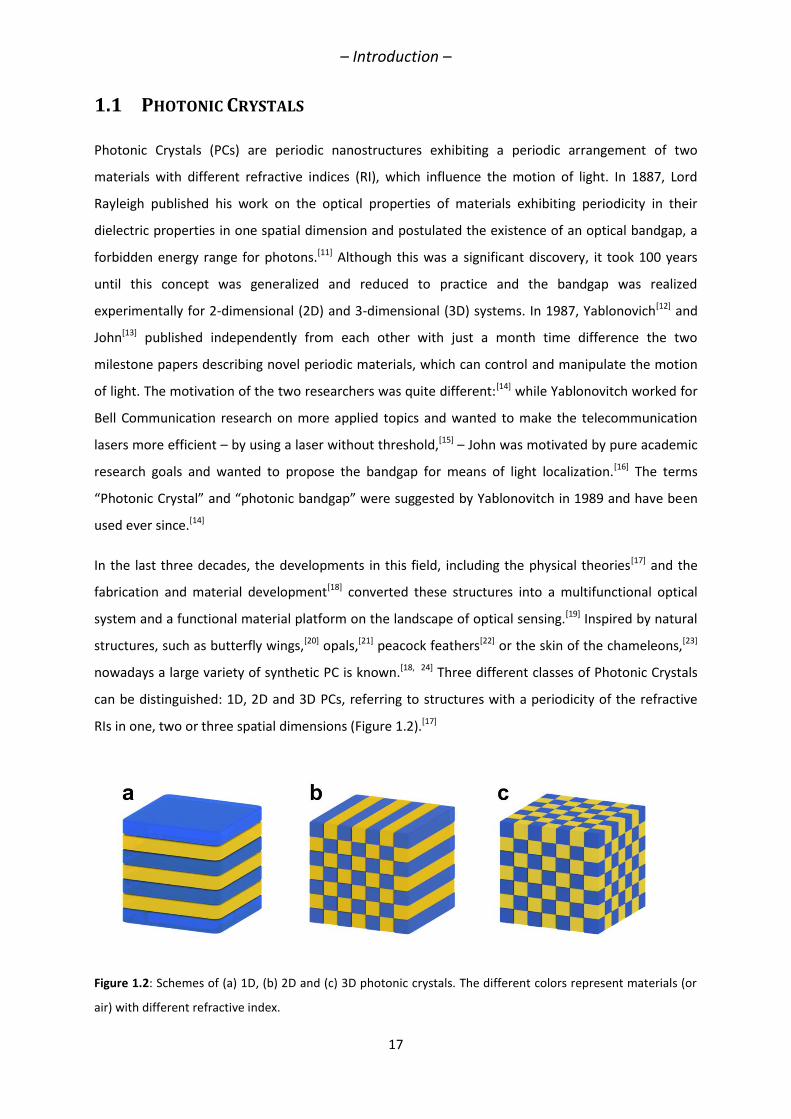
1.1 PHOTONIC CRYSTALS
Photonic Crystals (PCs) are periodic nanostructures exhibiting a periodic arrangement of two
materials with different refractive indices (RI), which influence the motion of light. In 1887, Lord
Rayleigh published his work on the optical properties of materials exhibiting periodicity in their
dielectric properties in one spatial dimension and postulated the existence of an optical bandgap, a
forbidden energy range for photons.[11] Although this was a significant discovery, it took 100 years
until this concept was generalized and reduced to practice and the bandgap was realized
experimentally for 2-dimensional (2D) and 3-dimensional (3D) systems. In 1987, Yablonovich[12] and
John[13] published independently from each other with just a month time difference the two
milestone papers describing novel periodic materials, which can control and manipulate the motion
of light. The motivation of the two researchers was quite different:[14] while Yablonovitch worked for
Bell Communication research on more applied topics and wanted to make the telecommunication
lasers more efficient – by using a laser without threshold,[15] – John was motivated by pure academic
research goals and wanted to propose the bandgap for means of light localization.[16] The terms
“Photonic Crystal” and “photonic bandgap” were suggested by Yablonovitch in 1989 and have been
used ever since.[14]
In the last three decades, the developments in this field, including the physical theories[17] and the
fabrication and material development[18] converted these structures into a multifunctional optical
system and a functional material platform on the landscape of optical sensing.[19] Inspired by natural
structures, such as butterfly wings,[20] opals,[21] peacock feathers[22] or the skin of the chameleons,[23]
nowadays a large variety of synthetic PC is known.[18, 24] Three different classes of Photonic Crystals
can be distinguished: 1D, 2D and 3D PCs, referring to structures with a periodicity of the refractive
RIs in one, two or three spatial dimensions (Figure 1.2).[17]
Figure 1.2: Schemes of (a) 1D, (b) 2D and (c) 3D photonic crystals. The different colors represent materials (or
air) with different refractive index.
– Introduction –
18
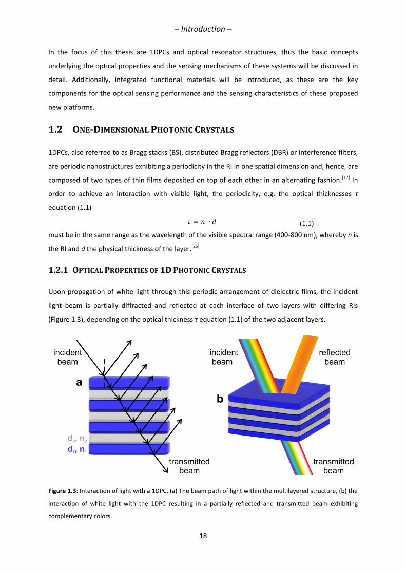
In the focus of this thesis are 1DPCs and optical resonator structures, thus the basic concepts
underlying the optical properties and the sensing mechanisms of these systems will be discussed in
detail. Additionally, integrated functional materials will be introduced, as these are the key
components for the optical sensing performance and the sensing characteristics of these proposed
new platforms.
1.2 ONE-DIMENSIONAL PHOTONIC CRYSTALS
1DPCs, also referred to as Bragg stacks (BS), distributed Bragg reflectors (DBR) or interference filters,
are periodic nanostructures exhibiting a periodicity in the RI in one spatial dimension and, hence, are
composed of two types of thin films deposited on top of each other in an alternating fashion.[17] In
order to achieve an interaction with visible light, the periodicity, e.g. the optical thicknesses τ
equation (1.1)
(1.1)
must be in the same range as the wavelength of the visible spectral range (400-800 nm), whereby n is
the RI and d the physical thickness of the layer.[25]
1.2.1 OPTICAL PROPERTIES OF 1D PHOTONIC CRYSTALS
Upon propagation of white light through this periodic arrangement of dielectric films, the incident
light beam is partially diffracted and reflected at each interface of two layers with differing RIs
(Figure 1.3), depending on the optical thickness τ equation (1.1) of the two adjacent layers.
Figure 1.3: Interaction of light with a 1DPC. (a) The beam path of light within the multilayered structure, (b) the
interaction of white light with the 1DPC resulting in a partially reflected and transmitted beam exhibiting
complementary colors.
– Introduction –
19
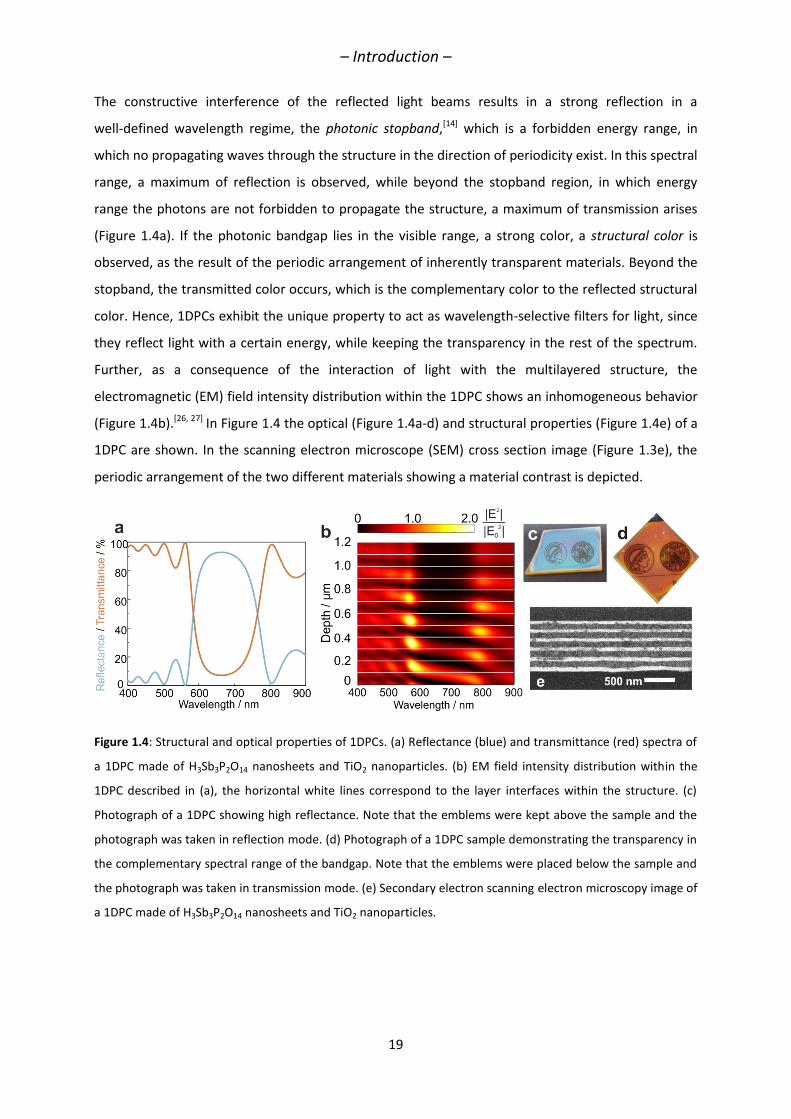
The constructive interference of the reflected light beams results in a strong reflection in a
well-defined wavelength regime, the photonic stopband,[14] which is a forbidden energy range, in
which no propagating waves through the structure in the direction of periodicity exist. In this spectral
range, a maximum of reflection is observed, while beyond the stopband region, in which energy
range the photons are not forbidden to propagate the structure, a maximum of transmission arises
(Figure 1.4a). If the photonic bandgap lies in the visible range, a strong color, a structural color is
observed, as the result of the periodic arrangement of inherently transparent materials. Beyond the
stopband, the transmitted color occurs, which is the complementary color to the reflected structural
color. Hence, 1DPCs exhibit the unique property to act as wavelength-selective filters for light, since
they reflect light with a certain energy, while keeping the transparency in the rest of the spectrum.
Further, as a consequence of the interaction of light with the multilayered structure, the
electromagnetic (EM) field intensity distribution within the 1DPC shows an inhomogeneous behavior
(Figure 1.4b).[26, 27] In Figure 1.4 the optical (Figure 1.4a-d) and structural properties (Figure 1.4e) of a
1DPC are shown. In the scanning electron microscope (SEM) cross section image (Figure 1.3e), the
periodic arrangement of the two different materials showing a material contrast is depicted.
Figure 1.4: Structural and optical properties of 1DPCs. (a) Reflectance (blue) and transmittance (red) spectra of
a 1DPC made of H3Sb3P2O14 nanosheets and TiO2 nanoparticles. (b) EM field intensity distribution within the
1DPC described in (a), the horizontal white lines correspond to the layer interfaces within the structure. (c)
Photograph of a 1DPC showing high reflectance. Note that the emblems were kept above the sample and the
photograph was taken in reflection mode. (d) Photograph of a 1DPC sample demonstrating the transparency in
the complementary spectral range of the bandgap. Note that the emblems were placed below the sample and
the photograph was taken in transmission mode. (e) Secondary electron scanning electron microscopy image of
a 1DPC made of H3Sb3P2O14 nanosheets and TiO2 nanoparticles.
– Introduction –
20
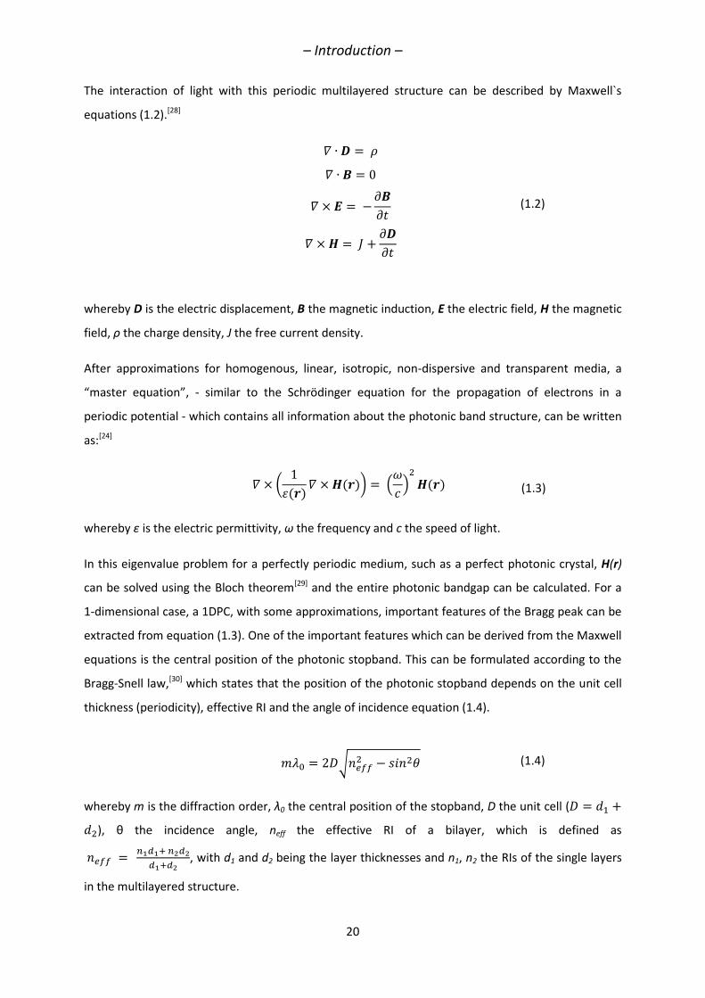
The interaction of light with this periodic multilayered structure can be described by Maxwell`s
equations (1.2).[28]
(1.2)
whereby D is the electric displacement, B the magnetic induction, E the electric field, H the magnetic
field, ρ the charge density, J the free current density.
After approximations for homogenous, linear, isotropic, non-dispersive and transparent media, a
“master equation”, - similar to the Schrödinger equation for the propagation of electrons in a
periodic potential - which contains all information about the photonic band structure, can be written
as:[24]
(1.3)
whereby ε is the electric permittivity, ω the frequency and c the speed of light.
In this eigenvalue problem for a perfectly periodic medium, such as a perfect photonic crystal, H(r)
can be solved using the Bloch theorem[29] and the entire photonic bandgap can be calculated. For a
1-dimensional case, a 1DPC, with some approximations, important features of the Bragg peak can be
extracted from equation (1.3). One of the important features which can be derived from the Maxwell
equations is the central position of the photonic stopband. This can be formulated according to the
Bragg-Snell law,[30] which states that the position of the photonic stopband depends on the unit cell
thickness (periodicity), effective RI and the angle of incidence equation (1.4).
(1.4)
whereby m is the diffraction order, λ0 the central position of the stopband, D the unit cell (
), θ the incidence angle, neff the effective RI of a bilayer, which is defined as
, with d1 and d2 being the layer thicknesses and n1, n2 the RIs of the single layers
in the multilayered structure.
– Introduction –
21
For normal incidence angle, this equation simplifies to equation (1.5)
(1.5)
Further, the reflectance intensity and the bandwidth of the stopband can be estimated by the
equations (1.6) and (1.7), respectively:
(1.6)
and
(1.7)
whereby n0 is the RI of the surrounding medium, ns the RI of the substrate, nl the RI of the low RI
material, nh the RI of the high RI material, and N the number of bilayers.[19]
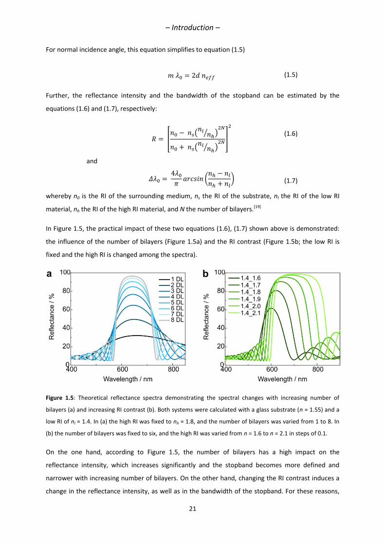
In Figure 1.5, the practical impact of these two equations (1.6), (1.7) shown above is demonstrated:
the influence of the number of bilayers (Figure 1.5a) and the RI contrast (Figure 1.5b; the low RI is
fixed and the high RI is changed among the spectra).
Figure 1.5: Theoretical reflectance spectra demonstrating the spectral changes with increasing number of
bilayers (a) and increasing RI contrast (b). Both systems were calculated with a glass substrate (n = 1.55) and a
low RI of nl = 1.4. In (a) the high RI was fixed to nh = 1.8, and the number of bilayers was varied from 1 to 8. In
(b) the number of bilayers was fixed to six, and the high RI was varied from n = 1.6 to n = 2.1 in steps of 0.1.
On the one hand, according to Figure 1.5, the number of bilayers has a high impact on the
reflectance intensity, which increases significantly and the stopband becomes more defined and
narrower with increasing number of bilayers. On the other hand, changing the RI contrast induces a
change in the reflectance intensity, as well as in the bandwidth of the stopband. For these reasons,
– Introduction –
22
the design before the fabrication and the reverse engineering after the fabrication has an important
role to achieve tailor-made optical properties of these multilayered structures.
1.2.2 OPTICAL PROPERTIES OF RESONATORS
PCs are also called “semiconductors for light”[15] as they exhibit a characteristic bandgap for photons
arising from the periodicity in their dielectric properties, similar to “electronic semiconductors”
whose band gap arises from their periodic crystal structure and the resulting periodic potential for
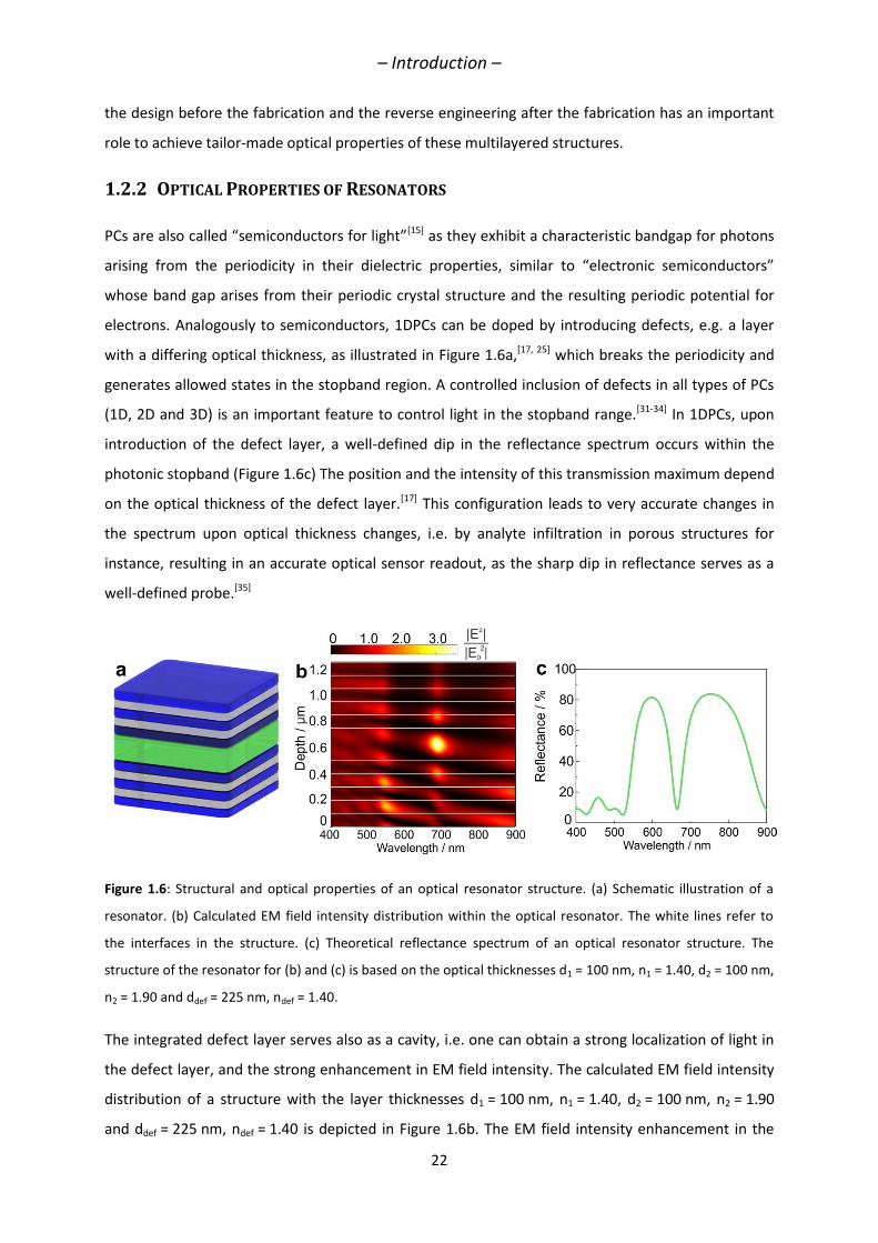
electrons. Analogously to semiconductors, 1DPCs can be doped by introducing defects, e.g. a layer
with a differing optical thickness, as illustrated in Figure 1.6a,[17, 25] which breaks the periodicity and
generates allowed states in the stopband region. A controlled inclusion of defects in all types of PCs
(1D, 2D and 3D) is an important feature to control light in the stopband range.[31-34] In 1DPCs, upon
introduction of the defect layer, a well-defined dip in the reflectance spectrum occurs within the
photonic stopband (Figure 1.6c) The position and the intensity of this transmission maximum depend
on the optical thickness of the defect layer.[17] This configuration leads to very accurate changes in
the spectrum upon optical thickness changes, i.e. by analyte infiltration in porous structures for
instance, resulting in an accurate optical sensor readout, as the sharp dip in reflectance serves as a
well-defined probe.[35]
Figure 1.6: Structural and optical properties of an optical resonator structure. (a) Schematic illustration of a
resonator. (b) Calculated EM field intensity distribution within the optical resonator. The white lines refer to
the interfaces in the structure. (c) Theoretical reflectance spectrum of an optical resonator structure. The
structure of the resonator for (b) and (c) is based on the optical thicknesses d1 = 100 nm, n1 = 1.40, d2 = 100 nm,
n2 = 1.90 and ddef = 225 nm, ndef = 1.40.
The integrated defect layer serves also as a cavity, i.e. one can obtain a strong localization of light in
the defect layer, and the strong enhancement in EM field intensity. The calculated EM field intensity
distribution of a structure with the layer thicknesses d1 = 100 nm, n1 = 1.40, d2 = 100 nm, n2 = 1.90
and ddef = 225 nm, ndef = 1.40 is depicted in Figure 1.6b. The EM field intensity enhancement in the
– Introduction –
23
cavity can lead to a strong modification of absorption[36] and emission[37] properties of an integrated
component and offers a possibility to utilize these in sensing applications.[32]
1.3 OPTICAL SENSING VIA PHOTONIC CRYSTALS
One of the application fields, which developed dynamically since the discovery of photonic crystals, is
the sensing field.[19, 38, 39] According to the Bragg-Snell law equation (1.5), the position of the photonic
stopband and with it, the structural color can be determined from the optical thicknesses of the
constituent layers. This not only means that the reflectance properties can be designed with the
careful fabrication of the structure, but thus also the structural color can be modified dynamically.
Once the optical thickness, e.g. the physical layer thickness or the RI, changes in response to external
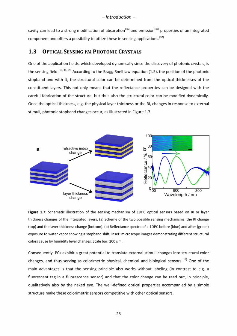
stimuli, photonic stopband changes occur, as illustrated in Figure 1.7.
Figure 1.7: Schematic illustration of the sensing mechanism of 1DPC optical sensors based on RI or layer
thickness changes of the integrated layers. (a) Scheme of the two possible sensing mechanisms: the RI change
(top) and the layer thickness change (bottom). (b) Reflectance spectra of a 1DPC before (blue) and after (green)
exposure to water vapor showing a stopband shift, inset: microscope images demonstrating different structural
colors cause by humidity level changes. Scale bar: 200 μm.
Consequently, PCs exhibit a great potential to translate external stimuli changes into structural color
changes, and thus serving as colorimetric physical, chemical and biological sensors.[19] One of the
main advantages is that the sensing principle also works without labeling (in contrast to e.g. a
fluorescent tag in a fluorescence sensor) and that the color change can be read out, in principle,
qualitatively also by the naked eye. The well-defined optical properties accompanied by a simple
structure make these colorimetric sensors competitive with other optical sensors.
– Introduction –
24
In the last three decades, numerous PC based optical sensors were reported for various sensing
applications and sensing analytes. Just to name some of the representative systems, various chemical
sensors for metal ions (Cu2+,[40] Pb2+,[41, 42] Ca2+,[43] Ba2+, K+, Zn2+[44]), for ionic strength and pH,[45] other
chemically and biologically relevant analytes, such as glucose,[40, 46] volatile organic compounds
(VOC),[47-[52] organic solvents,[53, 54] humidity,[55-57] for physical stimuli such as temperature[58, 59] or
pressure,[60, 61] and also various biological sensors[54, 62-64] were presented.
In the main focus of this thesis are functional material based 1DPCs and resonator structures for
vapor sensing applications, hence in the next chapter an overview of state-of-the-art VOC and
humidity sensors is presented.
1.3.1 FUNCTIONAL MATERIAL BASED SOLUTION PROCESSED 1D PHOTONIC CRYSTALS
FOR CHEMICAL SENSING APPLICATIONS
According to the Bragg-Snell law, equation (1.5), 1DPC based optical sensing relies on two main
mechanisms, first on the changes in RI upon analyte infiltration, and secondly on the changes in the
physical layer thickness. 1DPCs for which the sensing mechanism is based on the swelling or shrinking
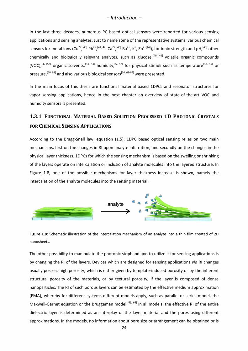
of the layers operate on intercalation or inclusion of analyte molecules into the layered structure. In
Figure 1.8, one of the possible mechanisms for layer thickness increase is shown, namely the
intercalation of the analyte molecules into the sensing material.
Figure 1.8: Schematic illustration of the intercalation mechanism of an analyte into a thin film created of 2D
nanosheets.
The other possibility to manipulate the photonic stopband and to utilize it for sensing applications is
by changing the RI of the layers. Devices which are designed for sensing applications via RI changes
usually possess high porosity, which is either given by template-induced porosity or by the inherent
structural porosity of the materials, or by textural porosity, if the layer is composed of dense
nanoparticles. The RI of such porous layers can be estimated by the effective medium approximation
(EMA), whereby for different systems different models apply, such as parallel or series model, the
Maxwell-Garnet equation or the Bruggeman model.[65, 66] In all models, the effective RI of the entire
dielectric layer is determined as an interplay of the layer material and the pores using different
approximations. In the models, no information about pore size or arrangement can be obtained or is
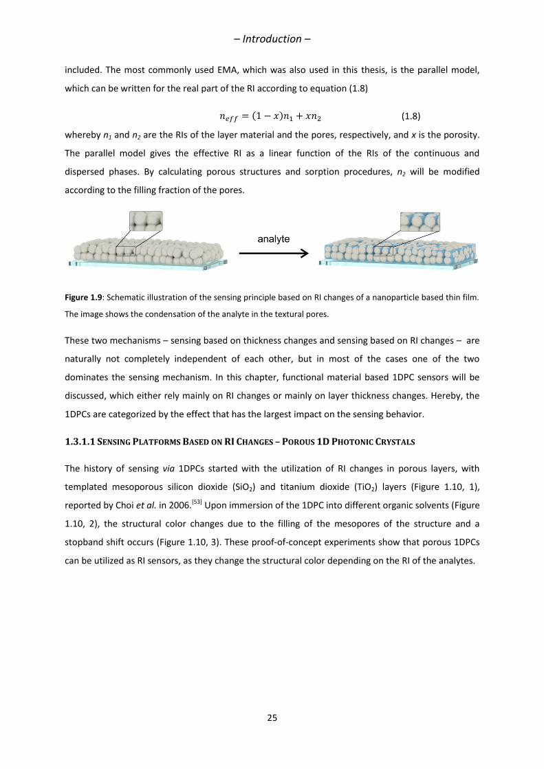
– Introduction –
25
included. The most commonly used EMA, which was also used in this thesis, is the parallel model,
which can be written for the real part of the RI according to equation (1.8)
(1.8)
whereby n1 and n2 are the RIs of the layer material and the pores, respectively, and x is the porosity.
The parallel model gives the effective RI as a linear function of the RIs of the continuous and
dispersed phases. By calculating porous structures and sorption procedures, n2 will be modified
according to the filling fraction of the pores.
Figure 1.9: Schematic illustration of the sensing principle based on RI changes of a nanoparticle based thin film.
The image shows the condensation of the analyte in the textural pores.
These two mechanisms – sensing based on thickness changes and sensing based on RI changes – are
naturally not completely independent of each other, but in most of the cases one of the two
dominates the sensing mechanism. In this chapter, functional material based 1DPC sensors will be
discussed, which either rely mainly on RI changes or mainly on layer thickness changes. Hereby, the
1DPCs are categorized by the effect that has the largest impact on the sensing behavior.
1.3.1.1 SENSING PLATFORMS BASED ON RI CHANGES – POROUS 1D PHOTONIC CRYSTALS
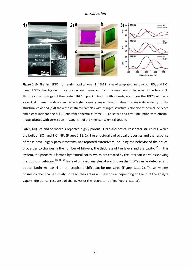
The history of sensing via 1DPCs started with the utilization of RI changes in porous layers, with
templated mesoporous silicon dioxide (SiO2) and titanium dioxide (TiO2) layers (Figure 1.10, 1),
reported by Choi et al. in 2006.[53] Upon immersion of the 1DPC into different organic solvents (Figure
1.10, 2), the structural color changes due to the filling of the mesopores of the structure and a
stopband shift occurs (Figure 1.10, 3). These proof-of-concept experiments show that porous 1DPCs
can be utilized as RI sensors, as they change the structural color depending on the RI of the analytes.
– Introduction –
26
Figure 1.10: The first 1DPCs for sensing applications. (1) SEM images of templated mesoporous SiO2 and TiO2
based 1DPCs showing (a-b) the cross section images and (c-d) the mesoporous character of the layers. (2)
Structural color changes of the created 1DPCs upon infiltration with solvents, (a-b) show the 1DPCs without a
solvent at normal incidence and at a higher viewing angle, demonstrating the angle dependency of the
structural color and (c-d) show the infiltrated samples with changed structural color also at normal incidence
and higher incident angle. (3) Reflectance spectra of three 1DPCs before and after infiltration with ethanol.
Image adapted with permission.[53]
Copyright of the American Chemical Society.
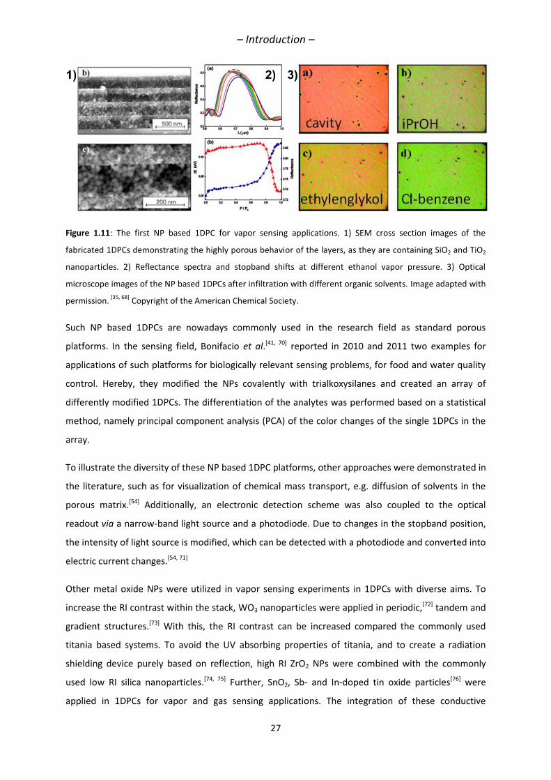
Later, Míguez and co-workers reported highly porous 1DPCs and optical resonator structures, which
are built of SiO2 and TiO2 NPs (Figure 1.11, 1). The structural and optical properties and the response
of these novel highly porous systems was reported extensively, including the behavior of the optical
properties to changes in the number of bilayers, the thickness of the layers and the cavity.[67] In this
system, the porosity is formed by textural pores, which are created by the interparticle voids showing
mesoporous behavior.[35, 68, 69] Instead of liquid analytes, it was shown that VOCs can be detected and
optical isotherms based on the stopband shifts can be measured (Figure 1.11, 2). These systems
posses no chemical sensitivity; instead, they act as a RI sensor, i.e. depending on the RI of the analyte
vapors, the optical response of the 1DPCs or the resonator differs (Figure 1.11, 3).
– Introduction –
27
Figure 1.11: The first NP based 1DPC for vapor sensing applications. 1) SEM cross section images of the
fabricated 1DPCs demonstrating the highly porous behavior of the layers, as they are containing SiO2 and TiO2
nanoparticles. 2) Reflectance spectra and stopband shifts at different ethanol vapor pressure. 3) Optical
microscope images of the NP based 1DPCs after infiltration with different organic solvents. Image adapted with
permission. [35, 68]
Copyright of the American Chemical Society.
Such NP based 1DPCs are nowadays commonly used in the research field as standard porous
platforms. In the sensing field, Bonifacio et al.[41, 70] reported in 2010 and 2011 two examples for
applications of such platforms for biologically relevant sensing problems, for food and water quality
control. Hereby, they modified the NPs covalently with trialkoxysilanes and created an array of
differently modified 1DPCs. The differentiation of the analytes was performed based on a statistical
method, namely principal component analysis (PCA) of the color changes of the single 1DPCs in the
array.
To illustrate the diversity of these NP based 1DPC platforms, other approaches were demonstrated in
the literature, such as for visualization of chemical mass transport, e.g. diffusion of solvents in the
porous matrix.[54] Additionally, an electronic detection scheme was also coupled to the optical
readout via a narrow-band light source and a photodiode. Due to changes in the stopband position,
the intensity of light source is modified, which can be detected with a photodiode and converted into
electric current changes.[54, 71]
Other metal oxide NPs were utilized in vapor sensing experiments in 1DPCs with diverse aims. To
increase the RI contrast within the stack, WO3 nanoparticles were applied in periodic,[72] tandem and
gradient structures.[73] With this, the RI contrast can be increased compared the commonly used
titania based systems. To avoid the UV absorbing properties of titania, and to create a radiation
shielding device purely based on reflection, high RI ZrO2 NPs were combined with the commonly
used low RI silica nanoparticles.[74, 75] Further, SnO2, Sb- and In-doped tin oxide particles[76] were
applied in 1DPCs for vapor and gas sensing applications. The integration of these conductive
– Introduction –
28
materials into such platforms is of interest, as an electric signal, such as the conductance change,
could be combined with the readout based on color changes.[25]
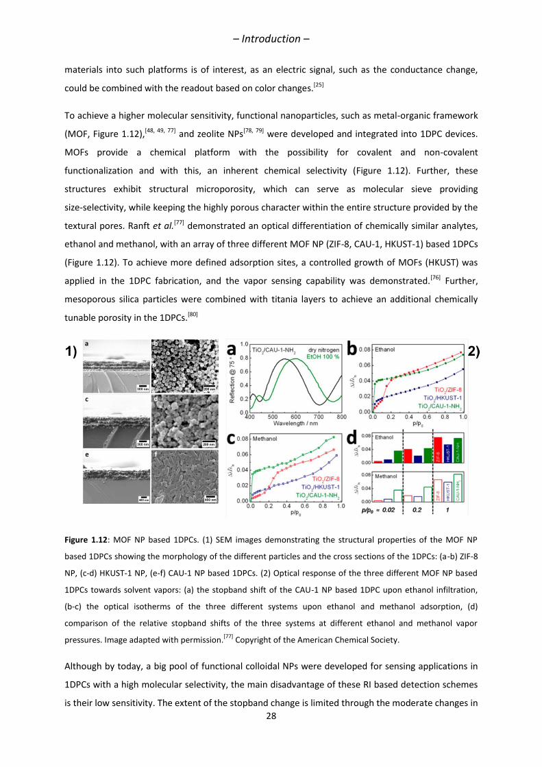
To achieve a higher molecular sensitivity, functional nanoparticles, such as metal-organic framework
(MOF, Figure 1.12),[48, 49, 77] and zeolite NPs[78, 79] were developed and integrated into 1DPC devices.
MOFs provide a chemical platform with the possibility for covalent and non-covalent
functionalization and with this, an inherent chemical selectivity (Figure 1.12). Further, these
structures exhibit structural microporosity, which can serve as molecular sieve providing
size-selectivity, while keeping the highly porous character within the entire structure provided by the
textural pores. Ranft et al.[77] demonstrated an optical differentiation of chemically similar analytes,
ethanol and methanol, with an array of three different MOF NP (ZIF-8, CAU-1, HKUST-1) based 1DPCs
(Figure 1.12). To achieve more defined adsorption sites, a controlled growth of MOFs (HKUST) was
applied in the 1DPC fabrication, and the vapor sensing capability was demonstrated.[76] Further,
mesoporous silica particles were combined with titania layers to achieve an additional chemically
tunable porosity in the 1DPCs.[80]
Figure 1.12: MOF NP based 1DPCs. (1) SEM images demonstrating the structural properties of the MOF NP
based 1DPCs showing the morphology of the different particles and the cross sections of the 1DPCs: (a-b) ZIF-8
NP, (c-d) HKUST-1 NP, (e-f) CAU-1 NP based 1DPCs. (2) Optical response of the three different MOF NP based
1DPCs towards solvent vapors: (a) the stopband shift of the CAU-1 NP based 1DPC upon ethanol infiltration,
(b-c) the optical isotherms of the three different systems upon ethanol and methanol adsorption, (d)
comparison of the relative stopband shifts of the three systems at different ethanol and methanol vapor
pressures. Image adapted with permission.[77]
Copyright of the American Chemical Society.
Although by today, a big pool of functional colloidal NPs were developed for sensing applications in
1DPCs with a high molecular selectivity, the main disadvantage of these RI based detection schemes
is their low sensitivity. The extent of the stopband change is limited through the moderate changes in
– Introduction –
29
the optical thickness of the layers, caused by the RI change, which translates only into rather small
stopband shifts, according to the Bragg-Snell law (1.5). To avoid this, 1DPCs with a swelling
component were developed to achieve larger stopband shifts.
1.3.1.2 SENSING PLATFORMS BASED ON LAYER THICKNESS CHANGES
In order to overcome the drawbacks of the RI change based detection principles and to enhance the
resolution due to larger optical thickness changes of the individual layers, devices were developed
where the physical layer thickness is modulated as a response to the presence of a vapor. This has a
higher impact on the optical thickness and with this also on the resolution and the sensitivity.[25]
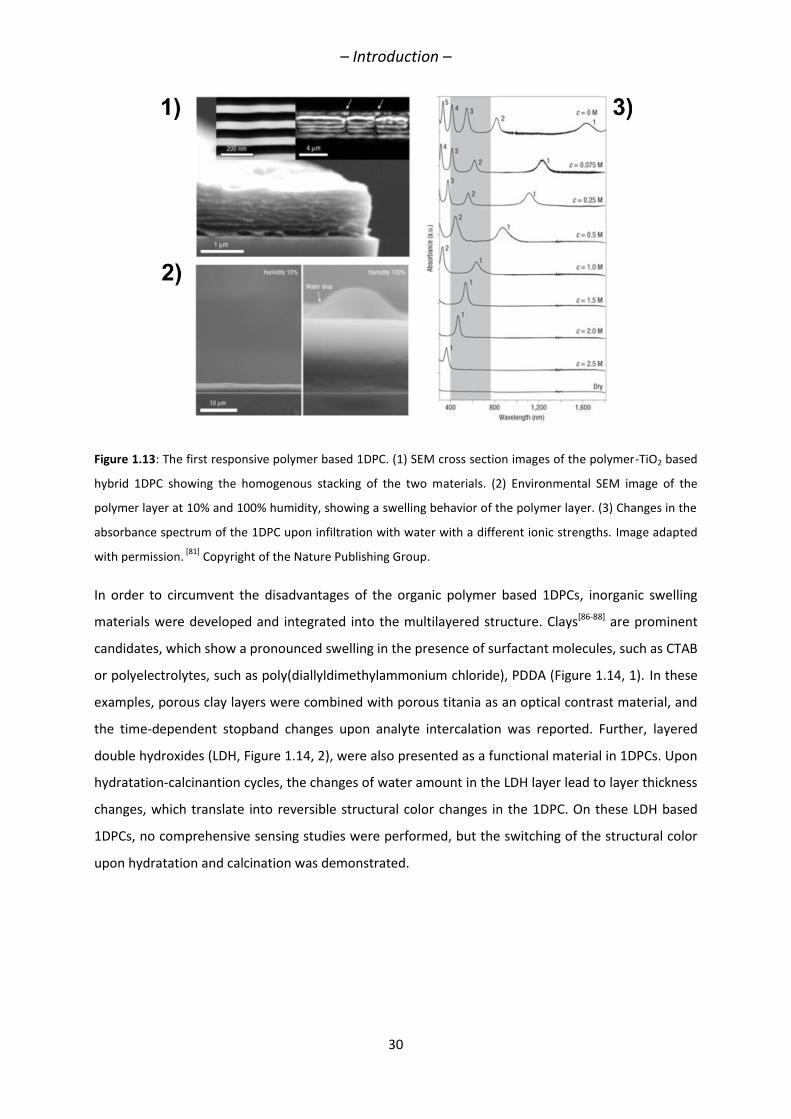
In 2007, shortly after the publication of the first solvent-responsive 1DPCs,[53] the first swelling 1DPCs
were reported (Figure 1.13).[81] In this work, polymer layers were used as the stimuli-responsive
material in a 1DPC, and upon infiltration with a liquid analyte, an enormous, full-spectral stopband
change was observed. Following this principle, many other polymer based 1DPCs were reported in
the last few years. One of the largest stopband changes was obtained by Tian et al.[57] applying a
hydrogel based 1DPC with a stopband shift of around 300 nm. Further, a plethora of hybrid
inorganic-organic polymer based structures were created for chemical vapor and solvent sensing and
detection approaches.[55, 82-85] Although the chemical selectivity can be fine-tuned through the
polymer composition, and the high sensitivity is given by the swelling mechanism, the chemical and
long-term stability of the organic layers and the slow response time in the range of several hours
present severe drawbacks of these systems.
– Introduction –
30
Figure 1.13: The first responsive polymer based 1DPC. (1) SEM cross section images of the polymer-TiO2 based
hybrid 1DPC showing the homogenous stacking of the two materials. (2) Environmental SEM image of the
polymer layer at 10% and 100% humidity, showing a swelling behavior of the polymer layer. (3) Changes in the
absorbance spectrum of the 1DPC upon infiltration with water with a different ionic strengths. Image adapted
with permission. [81]
Copyright of the Nature Publishing Group.
In order to circumvent the disadvantages of the organic polymer based 1DPCs, inorganic swelling
materials were developed and integrated into the multilayered structure. Clays[86-88] are prominent
candidates, which show a pronounced swelling in the presence of surfactant molecules, such as CTAB
or polyelectrolytes, such as poly(diallyldimethylammonium chloride), PDDA (Figure 1.14, 1). In these
examples, porous clay layers were combined with porous titania as an optical contrast material, and
the time-dependent stopband changes upon analyte intercalation was reported. Further, layered
double hydroxides (LDH, Figure 1.14, 2), were also presented as a functional material in 1DPCs. Upon
hydratation-calcinantion cycles, the changes of water amount in the LDH layer lead to layer thickness
changes, which translate into reversible structural color changes in the 1DPC. On these LDH based
1DPCs, no comprehensive sensing studies were performed, but the switching of the structural color
upon hydratation and calcination was demonstrated.
– Introduction –
31
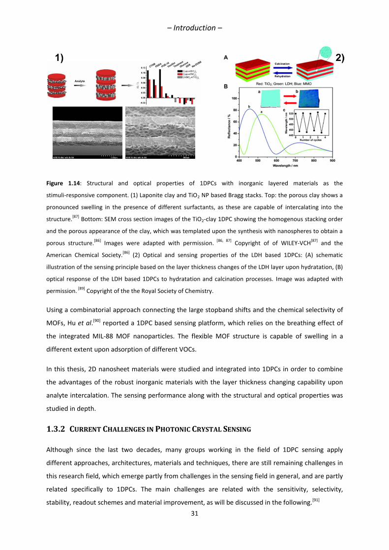
Figure 1.14: Structural and optical properties of 1DPCs with inorganic layered materials as the
stimuli-responsive component. (1) Laponite clay and TiO2 NP based Bragg stacks. Top: the porous clay shows a
pronounced swelling in the presence of different surfactants, as these are capable of intercalating into the
structure.[87]
Bottom: SEM cross section images of the TiO2-clay 1DPC showing the homogenous stacking order
and the porous appearance of the clay, which was templated upon the synthesis with nanospheres to obtain a
porous structure.[86]
Images were adapted with permission. [86, 87]
Copyright of of WILEY-VCH[87]
and the
American Chemical Society.[86]
(2) Optical and sensing properties of the LDH based 1DPCs: (A) schematic
illustration of the sensing principle based on the layer thickness changes of the LDH layer upon hydratation, (B)
optical response of the LDH based 1DPCs to hydratation and calcination processes. Image was adapted with
permission. [89]
Copyright of the the Royal Society of Chemistry.
Using a combinatorial approach connecting the large stopband shifts and the chemical selectivity of
MOFs, Hu et al.[90] reported a 1DPC based sensing platform, which relies on the breathing effect of
the integrated MIL-88 MOF nanoparticles. The flexible MOF structure is capable of swelling in a
different extent upon adsorption of different VOCs.
In this thesis, 2D nanosheet materials were studied and integrated into 1DPCs in order to combine
the advantages of the robust inorganic materials with the layer thickness changing capability upon
analyte intercalation. The sensing performance along with the structural and optical properties was
studied in depth.
1.3.2 CURRENT CHALLENGES IN PHOTONIC CRYSTAL SENSING
Although since the last two decades, many groups working in the field of 1DPC sensing apply
different approaches, architectures, materials and techniques, there are still remaining challenges in
this research field, which emerge partly from challenges in the sensing field in general, and are partly
related specifically to 1DPCs. The main challenges are related with the sensitivity, selectivity,
stability, readout schemes and material improvement, as will be discussed in the following.[91]
– Introduction –
32
The sensitivity of 1DPCs is mainly limited by small stopband shifts, as the majority of 1DPC
optical sensors are based on RI changes due to analyte infiltration. Usually, the filling of the
porous matrix translates into stopband shifts of some tens of nanometers at best. With
increasing stopband changes, the sensitivity (signal change per analyte concentration) and
the resolution can be increased, leading to possible naked-eye-readout or a detection
scheme based on a previous color calibration. This development would pave the way
towards photonic test stripes or other easy-to-use probe methods.
Based on the issue of low sensitivity and small signal changes, the readout schemes are
usually limited to reflectometry or interferometry, but these techniques are impracticable for
commercially used devices. In the last few years, several other approaches were developed
to bypass this technique. The electro-photonic nose was presented, whereby the stopband
shifts change the intensity of a narrow light source by changing the reflectance regime upon
analyte uptake. These light intensity variations could be translated by means of a photodiode
into electric current changes. Further, photoluminescence [92-94] and optical absorption due to
plasmonic effects[95] were combined with photonic structures and were also presented as an
attractive readout scheme.
Another aspect, the stability, is restricted in two different ways: the stability of the sensor
itself and the signal stability. On the one hand, upon storage, the sensing performance can be
altered, giving rise to the need for more frequent calibrations. On the other hand, the sensor
itself can be damaged or poisoned during the sensing event, which is highly unfavorable and
impractical for practical applications.
Finally, one of the largest issues in the sensing field in general is the selectivity and the cross
sensitivity to other chemically similar analytes. Many sensors in this field that do not rely on
molecular recognition or labeling schemes (biological sensors), are usually not chemically
selective and distinguish the analytes often only by RI or solvent polarity.[53, 69] In other
approaches, the selectivity issue is solved with complicated statistical data evaluation, such
as principal component analysis (PCA),[41, 70, 77] or with the application of complex hierarchical
structures.[52]
For these challenges, the development of novel sensing materials, which compensate for the above
shortcomings by featuring for example inherent chemical selectivity or a pronounced swelling
capability, is highly desired. Further, the optimization of existing materials in terms of
monodispersity, homogeneity and crystallinity can also be crucial to establish more efficient devices.
– Introduction –
33
1.4 2D MATERIALS
2D materials are crystalline materials with a thickness of a single layer of atoms or one
crystallographic unit cell, having a thickness in the range between 1 Å and 1 nm and lateral
dimensions of several hundreds of nanometers up to the micron range. Although the first crystalline
2D material, graphene, had already been studied theoretically by Wallace[96] and isolated and imaged
already in 1962 by Boehm et al.,[97] its “re-discovery”, followed by extensive experimental work and
characterization by Andre Geim and Konstantin Novoselov[98] tackled renewed research interest in
this carbon modification in the material science community. In 2010, Geim and Novoselov were
awarded with the Nobel Prize “for groundbreaking experiments regarding the two-dimensional
material graphene”.[99] The exceptional electronic, mechanical, thermal and optical properties differ
significantly from graphite, the three-dimensional (3D) bulk material, which can be lead back to the
unusual electronic and optical properties as well as the high anisotropy and size confinement effects
of the single layered hexagonal lattice of carbon atoms in graphene. After this first revolutionary
discovery, new ways were paved towards other classes of 2D materials, with an even wider scope of
physical and chemical properties.[100] The 2D materials discovered as of today show a rather broad
chemical variety, which gives the possibility for diverse applications as single nanosheets and also
rationally designed nanodevices[101] or hybrid artificial solids.[102-104]
1.4.1 EXFOLIATION
The synthesis methods of these single-layered nanosheets can be performed by different exfoliation
methods:[100] mechanical exfoliation or solution assisted exfoliation into stable colloidal suspensions.
Exfoliation is in general defined as a method, in which larger aggregates are decomposed into smaller
particles or nanosheets, whereby more specifically, if the bulk material is decomposed into single
nanosheets, the process is called delamination. The exfoliation method is mostly dependent on the
type of the bulk material. In the following, some general exfoliation routes will be presented.
The mechanical exfoliation includes methods such as the scotch tape method or rubbing the surface
of a layered crystalline material to another surface to obtain single or multilayered flakes.[98] Besides
graphene,[105] several inorganic van der Waals solids were isolated with this method, such as
MoS2[106, 107] or NbSe2.[108] Although this fabrication method is very straightforward and fast, single
layered nanosheets are produced only in the minority, compared to multilayered flakes, which limits
the scalability to larger scale production. For this reason, solvent assisted exfoliation methods are
more preferred for a sufficient nanosheet fabrication.
– Introduction –
34
Solvent-mediated exfoliation methods were reported in the literature for manifold nanosheet
compositions,[109-119] which can result in lateral sizes of several microns. Further, the separation of
single layered sheets from multilayered flakes is very straightforward by means of sedimentation or
centrifugation. Groundbreaking works on solution processed exfoliation were reported already in the
1990s by Sasaki et al.,[120-121] whereby the exfoliation of single nanosheets was proved by diverse
methods. Only one decade later, with the rediscovery of graphene and the increasing research
interest for 2D materials, these exfoliation methods gain in importance as they make a broad palette
of nanosheet materials accessible.[122-123] Since these developments, several solution based
exfoliation methods, aiming at the disruption of the attractive interlayer forces, were developed and
adapted for the materials to be exfoliated. In the following the exfoliation methods for the two main
types: van der Waals solids and layered ionic materials, are presented.
Van der Waals solids are layered bulk materials, which consist of neutral (i.e. non-charged) layers of
atoms with rather weak van der Waals interlayer bonding. For van der Waals solids, besides the
straightforward but less efficient scotch tape method, different solvent mediated exfoliation routes
were presented. The most straightforward method is the mechanical exfoliation of the layered
structure by ultrasound treatment of the bulk material in an appropriate solvent.[117] The choice of
the solvent depends on the chemical properties and the surface tension of the bulk material,
whereby for a sufficient exfoliation, the solvent molecules intercalate the van der Waals solid,
weaken the interlayer interactions and upon sonication, the bulk material is exfoliated. The drawback
of this method is that not only single layer nanosheets are observed, but also multilayered flakes.
Another method, which circumvents this disadvantage, is the reductive or oxidative intercalation
with a subsequent exfoliation. One example is the intercalation of lithium via electrochemical routes
or chemical methods. By a subsequent sonication step, single layered nanosheets are observed with
a large lateral size. In this process, most probably lithium reduces the bulk material (metal center) in
the first step. Upon contact with water, the metal center is oxidized again and caused by hydrogen
production, the bulk material delaminates into single nanosheets.[110, 124, 125] Further, the chemical
oxidation of the bulk material can lead to the introduction of repulsive forces, such as the oxidation
of graphite to graphene oxide, which significantly facilitates its subsequent exfoliation in polar
solvents such as water.[126] For the reductive and oxidative intercalation methods, a subsequent
stabilization by electrostatic forces[118] or surfactants[127] is needed to prevent agglomeration.
Layered ionic solids are bulk materials consisting of negatively or positively charged crystallographic
layers, whereby charge compensating anions or cations are located in the interlayer space. For
layered ionic materials, different solvent-mediated exfoliation routes are available. The simplest
method, which only applies for specific bulk materials, is the spontaneous exfoliation by stirring,
– Introduction –
35
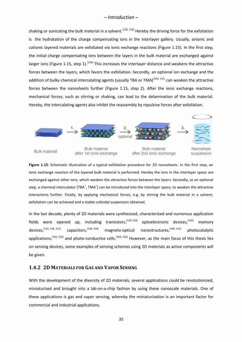
shaking or sonicating the bulk material in a solvent.[128, 129] Hereby the driving force for the exfoliation
is the hydratation of the charge compensating ions in the interlayer gallery. Usually, anionic and
cationic layered materials are exfoliated via ionic exchange reactions (Figure 1.15). In the first step,
the initial charge compensating ions between the layers in the bulk material are exchanged against
larger ions (Figure 1.15, step 1).[130] This increases the interlayer distance and weakens the attractive
forces between the layers, which favors the exfoliation. Secondly, an optional ion exchange and the
addition of bulky chemical intercalating agents (usually TBA or TMA)[104, 131] can weaken the attractive
forces between the nanosheets further (Figure 1.15, step 2). After the ionic exchange reactions,
mechanical forces, such as stirring or shaking, can lead to the delamination of the bulk material.
Hereby, the intercalating agents also inhibit the reassembly by repulsive forces after exfoliation.
Figure 1.15: Schematic illustration of a typical exfoliation procedure for 2D nanosheets. In the first step, an
ionic exchange reaction of the layered bulk material is performed. Hereby the ions in the interlayer space are
exchanged against other ions, which weaken the attractive forces between the layers. Secondly, as an optional
step, a chemical intercalator (TBA+, TMA
+) can be introduced into the interlayer space, to weaken the attractive
interactions further. Finally, by applying mechanical forces, e.g. by stirring the bulk material in a solvent,
exfoliation can be achieved and a stable colloidal suspension obtained.
In the last decade, plenty of 2D materials were synthesized, characterized and numerous application
fields were opened up, including transistors,[132-134] optoelectronic devices,[135] memory
devices,[132, 136, 137] capacitors,[138, 139] magneto-optical nanostructures,[140, 141] photocatalytic
applications,[142, 143] and photo-conductive cells.[144, 145] However, as the main focus of this thesis lies
on sensing devices, some examples of sensing schemes using 2D materials as active components will
be given.
1.4.2 2D MATERIALS FOR GAS AND VAPOR SENSING
With the development of the diversity of 2D materials, several applications could be revolutionized,
miniaturized and brought into a lab-on-a-chip fashion by using these nanoscale materials. One of
these applications is gas and vapor sensing, whereby the miniaturization is an important factor for
commercial and industrial applications.
– Introduction –
36
Most of the presented 2D material based sensor devices rely on electronic changes of the sample.
Upon adsorption, the sensing material can act as an electron donor or acceptor to the adsorbed gas
molecules, and the electric properties, such as resistivity or conductivity can change and be
measured. Many examples based on different readout schemes were presented in the last few years;
here a selection of the most important principles and examples is presented.
Chemiresistive sensors are capable of changing the resistivity upon analyte adsorption. Using this
technique, a broad palette of chemical analytes, such as humidity,[146-150] mercury vapor,[151]
triethylamine,[152, 153] methane,[154] ammonia[155] or VOCs[156] could be reliably detected by MoS2,
functionalized MoS2, SnS2 or VS2 nanosheet based devices. MoS2 and graphene based devices were
further used in field effect transistor (FET) based sensors for environmental monitoring, such as
ethanol,[157] hydrogen,[158] NO,[159] NO2[160] or ammonia[161] detection. FETs have some advantages,
such as portability, the capability for miniaturization and their high sensitivity, which makes these
types of sensors important candidates in this group. In FETs, a semiconductor channel, the sensing
material, connects the metal electrodes, the source and the drain. Upon analyte adsorption, the
drain current flowing from the source to the drain, is modulated, which gives the sensing signal.[162]
Further, 2D nanosheet material based Fabry-Pérot devices were fabricated for humidity and VOC
sensing applications, whereby all fabricated thin film devices act as optical sensors and the
interference color change based on the layer thickness changes can be detected. The layer thickness
changes, in turn, were induced by intercalation of the analyte molecules in the interlayer space of
the randomly restacked nanosheet based thin films.[163]
1.5 OBJECTIVES
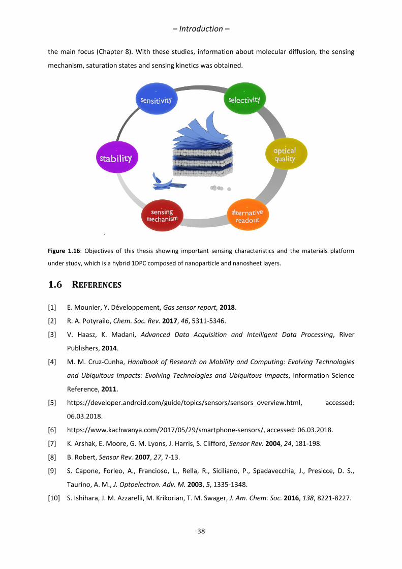
The main goal of this thesis was to tackle salient challenges (such as sensor and signal stability,
selectivity, sensitivity, the development of simple readout schemes, higher optical quality and the
exploration of new sensing materials) in 1DPC based optical sensors. These challenges were
addressed through the integration of environmentally responsive functional materials into 1DPCs.
Specifically, inorganic 2D nanosheets were synthesized, exfoliated into stable colloidal suspensions
and integrated into 1DPCs, which were then characterized in terms of their structure, morphology,
and sensing characteristics.
The first objective was to increase the stopband shifts by using swellable materials, which results in
larger sensing signals and higher sensitivity and signal resolution. The aim of the first project was to
integrate 2D antimony phosphate (H3Sb3P2O14) nanosheets into 1DPCs, as these are known to swell in
their bulk form in the presence of ambient water. By utilizing the enhanced sensitivity of the
– Introduction –
37
exfoliated nanosheets towards water vapor, a further goal of this project was to realize other sensing
approaches additionally to conventional humidity sensors. Inspired by the high sensitivity, one
attempt hereby was to realize touchless positioning devices, which are able to track very small
humidity changes in a very short time, such as the humidity gradient of the human finger (Chapter 3)
and characterizing these novel sensors (Chapter 4).
The second aim was to realize high selectivity towards a certain analyte whilst enabling the sensor to
identify also other analytes or vapor mixtures, similar to photonic nose applications. For this project,
another member of the antimony phosphate family, HSbP2O8, was integrated into 1DPCs, and the
optical response based on the intercalation of analyte molecules was tested for several VOCs and
VOC mixtures (Chapter 5). Furthermore, simple sensing descriptors, such as saturation time and
stopband shift, were analyzed.
A further goal of this thesis was to improve the optical properties of these functional 1DPCs whilst
maintaining good sensing performance. For this goal, another type of nanosheets, namely ultrahigh
RI lithium tin sulfides, were integrated into 1DPCs. In these systems the optical contrast increases
due to the high RI of the nanosheets, which leads to a better optical quality, e.g. higher reflectance
intensities with less deposited layers and, hence, decreased material costs. As these structures are
still highly receptive for ambient water molecules, the sensitivity towards water vapor is still present.
A further goal was to demonstrate the variability of this system, i.e. to combine the nanosheets with
different types of NPs or other nanosheet materials and thus to create hybrid structures with
enhanced or novel optical and sensing properties (Chapter 6).
In chapter 7, we aimed to address alternative readout schemes besides reflectometry or
spectrophotometry. Hereby, we combined the photonic environment with photoluminescent dyes,
whose emissive properties are changed depending on the local photonic environment. In order to
obtain tailor-made optical properties, a careful theoretical design of the hierarchical photonic
structures was necessary, which was done in collaboration with the group of Prof. Hernán Míguez,
ICMSE-CSIC, Sevilla, Spain.
Finally, a target of this thesis was to monitor the time-dependent infiltration and propagation of
analytes within the photonic structure in order to understand the intercalation mechanism and the
molecular diffusion within hybrid nanosheet – nanoparticle 1DPCs. To this end, an experimental set-
up was designed which enables the tracking of analytes through the structure. Further, theoretical
analysis of the optical measurements by fitting the reflectance spectra and analyzing the
time-dependent evolution and diffusion of the analyte molecules into the multilayered structure was
– Introduction –
38
the main focus (Chapter 8). With these studies, information about molecular diffusion, the sensing
mechanism, saturation states and sensing kinetics was obtained.
Figure 1.16: Objectives of this thesis showing important sensing characteristics and the materials platform
under study, which is a hybrid 1DPC composed of nanoparticle and nanosheet layers.
1.6 REFERENCES
[1] E. Mounier, Y. Développement, Gas sensor report, 2018.
[2] R. A. Potyrailo, Chem. Soc. Rev. 2017, 46, 5311-5346.
[3] V. Haasz, K. Madani, Advanced Data Acquisition and Intelligent Data Processing, River
Publishers, 2014.
[4] M. M. Cruz-Cunha, Handbook of Research on Mobility and Computing: Evolving Technologies
and Ubiquitous Impacts: Evolving Technologies and Ubiquitous Impacts, Information Science
Reference, 2011.
[5] https://developer.android.com/guide/topics/sensors/sensors_overview.html, accessed:
06.03.2018.
[6] https://www.kachwanya.com/2017/05/29/smartphone-sensors/, accessed: 06.03.2018.
[7] K. Arshak, E. Moore, G. M. Lyons, J. Harris, S. Clifford, Sensor Rev. 2004, 24, 181-198.
[8] B. Robert, Sensor Rev. 2007, 27, 7-13.
[9] S. Capone, Forleo, A., Francioso, L., Rella, R., Siciliano, P., Spadavecchia, J., Presicce, D. S.,
Taurino, A. M., J. Optoelectron. Adv. M. 2003, 5, 1335-1348.
[10] S. Ishihara, J. M. Azzarelli, M. Krikorian, T. M. Swager, J. Am. Chem. Soc. 2016, 138, 8221-8227.
– Introduction –
39
[11] L. Rayleigh, The London, Edinburgh, and Dublin Philosophical Magazine and Journal of Science
1887, 24, 145-159.
[12] E. Yablonovitch, Phys. Rev. Lett. 1987, 58, 2059-2062.
[13] S. John, Phys. Rev. Lett. 1987, 58, 2486-2489.
[14] K. Tsakmakidis, Nat. Mater. 2012, 11, 1000.
[15] E. Yablonovitch, Scientific American 2001, 285, 47-55.
[16] S. John, Nat. Mater. 2012, 11, 997.
[17] J. D. Joannopoulos, S. G. Johnson, J. N. Winn, R. D. Meade, Photonic crystals: molding the flow
of light, Princeton university press, 2011.
[18] C. López, Adv. Mater. 2003, 15, 1679-1704.
[19] J. Ge, Y. Yin, Angew. Chem. Int. Ed. 2011, 50, 1492-1522.
[20] W. Keiichiro, H. Takayuki, K. Kazuhiro, H. Yuichi, M. Shinji, Jpn. J. Appl. Phys. 2005, 44, L48.
[21] C. I. Aguirre, E. Reguera, A. Stein, Adv. Funct. Mater. 2010, 20, 2565-2578.
[22] J. Zi, X. Yu, Y. Li, X. Hu, C. Xu, X. Wang, X. Liu, R. Fu, P. Natl. A. Sci. 2003, 100, 12576-12578.
[23] J. Teyssier, S. V. Saenko, D. van der Marel, M. C. Milinkovitch, Nat. Commun. 2015, 6, 6368.
[24] G. von Freymann, V. Kitaev, B. V. Lotsch, G. A. Ozin, Chem. Soc. Rev. 2013, 42, 2528-2554.
[25] L. D. Bonifacio, B. V. Lotsch, D. P. Puzzo, F. Scotognella, G. A. Ozin, Adv. Mater. 2009, 21,
1641-1646.
[26] P. Yeh, Optical Waves in Layered Media, John Wiley & Sons, New York, 1988.
[27] L. Novotny, B. Hecht., Principles of Nano-Optics, Cambridge University Press, 2012.
[28] J. C. Maxwell, Philos. T. R. Soc. Lond. 1865, 155, 459-512.
[29] F. Bloch, Z. Physik 1929, 52, 555-600.
[30] G. A. Ozin, A. C. Arsenault, L. Cademartiri, R. S. o. Chemistry, Nanochemistry: A Chemical
Approach to Nanomaterials, Royal Society of Chemistry, 2009.
[31] M. E. Calvo, S. Colodrero, N. Hidalgo, G. Lozano, C. Lopez-Lopez, O. Sanchez-Sobrado, H.
Miguez, Energ. Environ. Sci. 2011, 4, 4800-4812.
[32] Y.-n. Zhang, Y. Zhao, R.-q. Lv, Sensor Actuat. A: Phys. 2015, 233, 374-389.
[33] P. V. Braun, S. A. Rinne, F. García-Santamaría, Adv. Mater. 2006, 18, 2665-2678.
[34] J. D. Joannopoulos, P. R. Villeneuve, S. Fan, Nature 1997, 386, 143-149.
[35] S. Colodrero, M. Ocana, A. R. Gonzalez-Elipe, H. Miguez, Langmuir 2008, 24, 9135-9139.
[36] O. Sánchez-Sobrado, G. Lozano, M. E. Calvo, A. Sánchez-Iglesias, L. M. Liz-Marzán, H. Míguez,
Adv. Mater. 2011, 23, 2108-2112.
[37] A. Jiménez-Solano, J. F. Galisteo-López, H. Míguez, Small 2015, 11, 2727-2732.
[38] R. V. Nair, R. Vijaya, Prog. Quant. Electron. 2010, 34, 89-134.
[39] H. Xu, P. Wu, C. Zhu, A. Elbaz, Z. Z. Gu, J. Mater. Chem. C 2013, 1, 6087-6098.
– Introduction –
40
[40] J. H. Holtz, S. A. Asher, Nature 1997, 389, 829-832.
[41] L. D. Bonifacio, G. A. Ozin, A. C. Arsenault, Small 2011, 7, 3153-3157.
[42] M. M. W. Muscatello, S. A. Asher, Adv. Funct. Mater. 2008, 18, 1186-1193.
[43] S. Chakravarty, J. Topol'ancik, P. Bhattacharya, S. Chakrabarti, Y. Kang, M. E. Meyerhoff, Opt.
Lett. 2005, 30, 2578-2580.
[44] S. A. Asher, A. C. Sharma, A. V. Goponenko, M. M. Ward, Anal. Chem. 2003, 75, 1676-1683.
[45] K. Lee, S. A. Asher, J. Am. Chem. Soc. 2000, 122, 9534-9537.
[46] Y.-J. Lee, S. A. Pruzinsky, P. V. Braun, Langmuir 2004, 20, 3096-3106.
[47] P. A. Snow, E. K. Squire, P. S. J. Russell, L. T. Canham, J. Appl. Phys. 1999, 86, 1781-1784.
[48] F. M. Hinterholzinger, A. Ranft, J. M. Feckl, B. Ruhle, T. Bein, B. V. Lotsch, J. Mater. Chem. 2012,
22, 10356-10362.
[49] A. Ranft, I. Pavlichenko, K. Szendrei, P. M. Zehetmaier, Y. Hu, A. von Mankowski, B. V. Lotsch,
Microporous Mesoporous Mater. 2015, 216, 216-224.
[50] C. McDonagh, C. S. Burke, B. D. MacCraith, Chem. Rev. 2008, 108, 400-422.
[51] H. Yang, P. Jiang, B. Jiang, J. Colloid Interface Sci. 2012, 370, 11-18.
[52] T. L. Kelly, A. Garcia Sega, M. J. Sailor, Nano Lett. 2011, 11, 3169-3173.
[53] S. Y. Choi, M. Mamak, G. von Freymann, N. Chopra, G. A. Ozin, Nano Lett. 2006, 6, 2456-2461.
[54] I. Pavlichenko, E. Broda, Y. Fukuda, K. Szendrei, A. K. Hatz, G. Scarpa, P. Lugli, C. Brauchle, B. V.
Lotsch, Mater. Horiz. 2015, 2, 299-308.
[55] Z. Wang, J. Zhang, J. Xie, C. Li, Y. Li, S. Liang, Z. Tian, T. Wang, H. Zhang, H. Li, W. Xu, B. Yang,
Adv. Funct. Mater. 2010, 20, 3784-3790.
[56] R. A. Barry, P. Wiltzius, Langmuir 2005, 22, 1369-1374.
[57] E. Tian, J. Wang, Y. Zheng, Y. Song, L. Jiang, D. Zhu, J. Mater. Chem. 2008, 18, 1116-1122.
[58] I. Pavlichenko, A. T. Exner, M. Guehl, P. Lugli, G. Scarpa, B. V. Lotsch, J. Phys. Chem. C 2011,
116, 298-305.
[59] I. Pavlichenko, A. T. Exner, M. Guehl, P. Lugli, G. Scarpa, B. V. Lotsch, J. Phys. Chem. C 2011,
116, 298-305.
[60] A. C. Arsenault, T. J. Clark, G. von Freymann, L. Cademartiri, R. Sapienza, J. Bertolotti, E. Vekris,
S. Wong, V. Kitaev, I. Manners, R. Z. Wang, S. John, D. Wiersma, G. A. Ozin, Nat. Mater. 2006,
5, 179-184.
[61] F. Castles, S. M. Morris, J. M. C. Hung, M. M. Qasim, A. D. Wright, S. Nosheen, S. S. Choi, B. I.
Outram, S. J. Elston, C. Burgess, L. Hill, T. D. Wilkinson, H. J. Coles, Nat. Mater. 2014, 13,
817-821.
[62] V. N. Konopsky, E. V. Alieva, Anal. Chem. 2007, 79, 4729-4735.
[63] M. R. Lee, P. M. Fauchet, Opt. Express 2007, 15, 4530-4535.
– Introduction –
41
[64] N. Skivesen, A. Têtu, M. Kristensen, J. Kjems, L. H. Frandsen, P. I. Borel, Opt. Express 2007, 15,
3169-3176.
[65] M. M. Braun, L. Pilon, Thin Solid Films 2006, 496, 505-514.
[66] N. Nagy, Deak, A., Horvölgyi, Z., Fried, M., Agod, A., Barsony, I., Langmuir 2006, 26, 8416-8423.
[67] M. E. Calvo, O. Sánchez-Sobrado, S. Colodrero, H. Míguez, Langmuir 2009, 25, 2443-2448.
[68] S. Colodrero, M. Ocaña, H. Míguez, Langmuir 2008, 24, 4430-4434.
[69] M. C. Fuertes, S. Colodrero, G. Lozano, A. R. González-Elipe, D. Grosso, C. Boissière, C. Sánchez,
G. J. d. A. A. Soler-Illia, H. Míguez, J. Phys. Chem. C 2008, 112, 3157-3163.
[70] L. D. Bonifacio, D. P. Puzzo, S. Breslav, B. M. Willey, A. McGeer, G. A. Ozin, Adv. Mater. 2010,
22, 1351-1354.
[71] A. T. Exner, I. Pavlichenko, D. Baierl, M. Schmidt, G. Derondeau, B. V. Lotsch, P. Lugli, G. Scarpa,
Laser Photonics Rev. 2014, 5, 726-733.
[72] E. Redel, P. Mirtchev, C. Huai, S. Petrov, G. A. Ozin, ACS Nano 2011, 5, 2861-2869.
[73] E. Redel, C. Huai, M. Renner, G. von Freymann, G. A. Ozin, Small 2011, 7, 3465-3471.
[74] M. E. Calvo, J. R. Castro Smirnov, H. Míguez, J. Polym. Sci., Part B: Polym. Phys. 2012, 50,
945-956.
[75] J. R. C. Smirnov, M. Ito, M. E. Calvo, C. López-López, A. Jiménez-Solano, J. F. Galisteo-López, P.
Zavala-Rivera, K. Tanaka, E. Sivaniah, H. Míguez, Adv. Opt. Mater. 2015, 3, 1633-1639.
[76] J. Liu, E. Redel, S. Walheim, Z. Wang, V. Oberst, J. Liu, S. Heissler, A. Welle, M. Moosmann, T.
Scherer, M. Bruns, H. Gliemann, C. Wöll, Chem. Mater. 2015, 27, 1991-1996.
[77] A. Ranft, F. Niekiel, I. Pavlichenko, N. Stock, B. V. Lotsch, Chem. Mater. 2015, 27, 1961–1970.
[78] B. V. Lotsch, F. Scotognella, K. Moeller, T. Bein, G. A. Ozin, Proc. SPIE, 7713, 2010, 7713V.
[79] K. Lazarova, H. Awala, S. Thomas, M. Vasileva, S. Mintova, T. Babeva, Sensors 2014, 14, 12207.
[80] J. Kobler, B. V. Lotsch, G. A. Ozin, T. Bein, ACS Nano 2009, 3, 1669-1676.
[81] Y. Kang, J. J. Walish, T. Gorishnyy, E. L. Thomas, Nat. Mater. 2007, 6, 957-960.
[82] R. Xuan, Q. Wu, Y. Yin, J. Ge, J. Mater. Chem. 2011, 21, 3672-3676.
[83] Z. Wang, J. Zhang, J. Li, J. Xie, Y. Li, S. Liang, Z. Tian, C. Li, Z. Wang, T. Wang, H. Zhang, B. Yang, J.
Mater. Chem. 2011, 21, 1264-1270.
[84] Z. Wang, J. Zhang, Z. Wang, H. Shen, J. Xie, Y. Li, L. Lin, B. Yang, J. Mater. Chem. C 2013, 1, 977-
983.
[85] K. G. Lazarova, R.; Vasileva, M.; Georgieva, B.; Spassova, M.; Malinowski, N.; Babeva, T., Opt.
Quantum Electron. 2016, 6.
[86] B. V. Lotsch, G. A. Ozin, ACS Nano 2008, 2, 2065-2074.
[87] B. V. Lotsch, G. A. Ozin, Adv. Mater. 2008, 20, 4079-4084.
[88] B. V. Lotsch, G. A. Ozin, J. Am. Chem. Soc. 2008, 130, 15252-15253.
– Introduction –
42
[89] J. Han, Y. Dou, M. Wei, D. G. Evans, X. Duan, RSC Adv. 2012, 2, 10488-10491.
[90] Z. Hu, C.-a. Tao, F. Wang, X. Zou, J. Wang, J. Mater. Chem. C 2015, 3, 211-216.
[91] C. Fenzl, T. Hirsch, O. S. Wolfbeis, Angew. Chem. Int. Ed. 2014, 53, 3318-3335.
[92] O. Sanchez-Sobrado, M. E. Calvo, N. Nunez, M. Ocana, G. Lozano, H. Miguez, Nanoscale 2010,
2, 936-941.
[93] M. Li, F. He, Q. Liao, J. Liu, L. Xu, L. Jiang, Y. Song, S. Wang, D. Zhu, Angew. Chem. Int. Ed. 2008,
120, 7368-7372.
[94] X. Zhao, Y. Cao, F. Ito, H.-H. Chen, K. Nagai, Y.-H. Zhao, Z.-Z. Gu, Angew. Chem. Int. Ed. 2006,
118, 6989-6992.
[95] M. Shaban, A. M. Ahmed, E. Abdel-Rahman, H. Hamdy, Sci. Rep. 2017, 7, 41983.
[96] P. R. Wallace, Phys. Rev. 1947, 71, 622-634.
[97] H. P. Boehm, A. Clauss, G. O. Fischer, U. Hofmann, Z. anorg. Allg. Chem. 1962, 316, 119-127.
[98] K. S. Novoselov, A. K. Geim, S. V. Morozov, D. Jiang, Y. Zhang, S. V. Dubonos, I. V. Grigorieva, A.
A. Firsov, Science 2004, 306, 666-669.
[99] https://www.nobelprize.org/nobel_prizes/physics/laureates/2010/, accessed 02.03.2018.
[100] R. Mas-Balleste, C. Gomez-Navarro, J. Gomez-Herrero, F. Zamora, Nanoscale 2011, 3, 20-30.
[101] K. J. Koski, Y. Cui, ACS Nano 2013, 7, 3739-3743.
[102] B. V. Lotsch, Annu. Rev. Mater. Res. 2015, 45, 85-109.
[103] L. Li, R. Ma, Y. Ebina, K. Fukuda, K. Takada, T. Sasaki, J. Am. Chem. Soc. 2007, 129, 8000-8007.
[104] C. Ziegler, S. Werner, M. Bugnet, M. Wörsching, V. Duppel, G. A. Botton, C. Scheu, B. V. Lotsch,
Chem. Mater. 2013, 25, 4892-4900.
[105] A. K. Geim, K. S. Novoselov, Nat. Mater. 2007, 6, 183-191.
[106] B. Radisavljevic, A. Radenovic, J. Brivio, V. Giacometti, A. Kis, Nat. Nanotechnol. 2011, 6,
147-150.
[107] S. Ghatak, A. N. Pal, A. Ghosh, ACS Nano 2011, 5, 7707-7712.
[108] K. S. Novoselov, D. Jiang, F. Schedin, T. J. Booth, V. V. Khotkevich, S. V. Morozov, A. K. Geim,
Proc. Natl. Acad. Sci. U.S.A. 2005, 102, 10451-10453.
[109] P. May, U. Khan, J. M. Hughes, J. N. Coleman, J. Phys. Chem. C 2012, 116, 11393-11400.
[110] Z. Zeng, Z. Yin, X. Huang, H. Li, Q. He, G. Lu, F. Boey, H. Zhang, Angew. Chem. Int. Ed. 2011, 50,
11093-11097.
[111] K.-G. Zhou, N.-N. Mao, H.-X. Wang, Y. Peng, H.-L. Zhang, Angew. Chem. Int. Ed. 2011, 50,
10839-10842.
[112] G. Cunningham, M. Lotya, C. S. Cucinotta, S. Sanvito, S. D. Bergin, R. Menzel, M. S. P. Shaffer, J.
N. Coleman, ACS Nano 2012, 6, 3468-3480.
– Introduction –
43
[113] F. Leroux, M. Adachi-Pagano, M. Intissar, S. Chauviere, C. Forano, J.-P. Besse, J. Mater. Chem.
2001, 11, 105-112.
[114] R. J. Smith, P. J. King, M. Lotya, C. Wirtz, U. Khan, S. De, A. O'Neill, G. S. Duesberg, J. C. Grunlan,
G. Moriarty, J. Chen, J. Wang, A. I. Minett, V. Nicolosi, J. N. Coleman, Adv. Mater. 2011, 23,
3944-3948.
[115] Z. Zeng, T. Sun, J. Zhu, X. Huang, Z. Yin, G. Lu, Z. Fan, Q. Yan, H. H. Hng, H. Zhang, Angew. Chem.
Int. Ed. 2012, 51, 9052-9056.
[116] M. B. Dines, Mater. Res. Bull. 1975, 10, 287-291.
[117] J. N. Coleman, M. Lotya, A. O'Neill, S. D. Bergin, P. J. King, U. Khan, K. Young, A. Gaucher, S. De,
R. J. Smith, I. V. Shvets, S. K. Arora, G. Stanton, H.-Y. Kim, K. Lee, G. T. Kim, G. S. Duesberg, T.
Hallam, J. J. Boland, J. J. Wang, J. F. Donegan, J. C. Grunlan, G. Moriarty, A. Shmeliov, R. J.
Nicholls, J. M. Perkins, E. M. Grieveson, K. Theuwissen, D. W. McComb, P. D. Nellist, V. Nicolosi,
Science 2011, 331, 568-571.
[118] P. Joensen, R. F. Frindt, S. R. Morrison, Mater. Res. Bull. 1986, 21, 457-461.
[119] G. Eda, H. Yamaguchi, D. Voiry, T. Fujita, M. Chen, M. Chhowalla, Nano Lett. 2011, 11,
5111-5116.
[120] T. Sasaki, M. Watanabe, H. Hashizume, H. Yamada, H. Nakazawa, J. Am. Chem. Soc. 1996, 118,
8329-8335.
[121] T. Sasaki, M. Watanabe, H. Hashizume, H. Yamada, H. Nakazawa, Chem. Commun. 1996,
229-230.
[122] H. Nakano, M. Ishii, H. Nakamura, Chem. Commun. 2005, 2945-2947.
[123] R. Ma, Z. Liu, L. Li, N. Iyi, T. Sasaki, J. Mater. Chem. 2006, 16, 3809-3813.
[124] V. Nicolosi, M. Chhowalla, M. G. Kanatzidis, M. S. Strano, J. N. Coleman, Science 2013, 340.
[125] S. Z. Butler, S. M. Hollen, L. Cao, Y. Cui, J. A. Gupta, H. R. Gutierrez, T. F. Heinz, S. S. Hong, J.
Huang, A. F. Ismach, E. Johnston-Halperin, M. Kuno, V. V. Plashnitsa, R. D. Robinson, R. S.
Ruoff, S. Salahuddin, J. Shan, L. Shi, M. G. Spencer, M. Terrones, W. Windl, J. E. Goldberger,
ACS Nano 2013, 7, 2898-2926.
[126] B. Vedhanarayanan, B. Babu, M. M. Shaijumon, A. Ajayaghosh, ACS Appl. Mater. Interfaces
2017, 9, 19417-19426.
[127] C.-J. Shih, A. Vijayaraghavan, R. Krishnan, R. Sharma, J.-H. Han, M.-H. Ham, Z. Jin, S. Lin, G. L. C.
Paulus, N. F. Reuel, Q. H. Wang, D. Blankschtein, M. S. Strano, Nat. Nanotechnol. 2011, 6, 439.
[128] A. Kuhn, T. Holzmann, J. Nuss, B. V. Lotsch, J. Mater. Chem. A 2014, 2, 6100-6106.
[129] T. Holzmann, L. M. Schoop, M. N. Ali, I. Moudrakovski, G. Gregori, J. Maier, R. J. Cava, B. V.
Lotsch, Energy Environ. Sci. 2016, 9, 2578-2585.
[130] M. A. Jobbágy, A. E. Regazzoni, J. Colloid Interface Sci. 2004, 275, 345-348.
– Introduction –
44
[131] L. Chang, M. A. Holmes, M. Waller, F. E. Osterloh, A. J. Moule, J. Mater. Chem. 2012, 22,
20443-20450.
[132] L. Britnell, R. V. Gorbachev, R. Jalil, B. D. Belle, F. Schedin, A. Mishchenko, T. Georgiou, M. I.
Katsnelson, L. Eaves, S. V. Morozov, N. M. R. Peres, J. Leist, A. K. Geim, K. S. Novoselov, L. A.
Ponomarenko, Science 2012, 335, 947-950.
[133] U. Zschieschang, T. Holzmann, A. Kuhn, M. Aghamohammadi, B. V. Lotsch, H. Klauk, J. Appl.
Phys. 2015, 117, 104509.
[134] W. J. Yu, Z. Li, H. Zhou, Y. Chen, Y. Wang, Y. Huang, X. Duan, Nat. Mater. 2012, 12, 246.
[135] Z.-G. Chen, J. Zou, G. Liu, F. Li, Y. Wang, L. Wang, X.-L. Yuan, T. Sekiguchi, H.-M. Cheng, G. Q. Lu,
ACS Nano 2008, 2, 2183-2191.
[136] G. Appala Naidu, N. A. Husam, S. Udo, J. Phys.: Condens. Matter 2017, 29, 035504.
[137] J. Lee, J.-H. Shin, G.-H. Lee, C.-H. Lee, Nanomaterials 2016, 6, 193.
[138] E. G. da Silveira Firmiano, A. C. Rabelo, C. J. Dalmaschio, A. N. Pinheiro, E. C. Pereira, W. H.
Schreiner, E. R. Leite, Adv. Energy Mater. 2014, 4, 1301380.
[139] L. Peng, X. Peng, B. Liu, C. Wu, Y. Xie, G. Yu, Nano Lett. 2013, 13, 2151-2157.
[140] Z. Liu, R. Ma, M. Osada, N. Iyi, Y. Ebina, K. Takada, T. Sasaki, J. Am. Chem. Soc. 2006, 128,
4872-4880.
[141] M. Osada, M. Itose, Y. Ebina, K. Ono, S. Ueda, K. Kobayashi, T. Sasaki, Appl. Phys. Lett. 2008, 92,
253110.
[142] B. Lin, P. Sun, Y. Zhou, S. Jiang, B. Gao, Y. Chen, J. Hazard. Mater. 2014, 280, 156-163.
[143] J. L. Gunjakar, T. W. Kim, H. N. Kim, I. Y. Kim, S.-J. Hwang, J. Am. Chem. Soc. 2011, 133,
14998-15007.
[144] N. Miyamoto, Y. Yamada, S. Koizumi, T. Nakato, Angew. Chem. Int. Ed. 2007, 46, 4123-4127.
[145] T. Yui, Y. Kobayashi, Y. Yamada, T. Tsuchino, K. Yano, T. Kajino, Y. Fukushima, T. Torimoto, H.
Inoue, K. Takagi, Phys. Chem. Chem. Phys. 2006, 8, 4585-4590.
[146] J. Feng, L. Peng, C. Wu, X. Sun, S. Hu, C. Lin, J. Dai, J. Yang, Y. Xie, Adv. Mater. 2012, 24,
1969-1974.
[147] S.-L. Zhang, H.-H. Choi, H.-Y. Yue, W.-C. Yang, Curr. Appl. Phys. 2014, 14, 264-268.
[148] W. M. R. Divigalpitiya, R. F. Frindt, S. R. Morrison, J. Phys. D: Appl. Phys. 1990, 23, 966.
[149] S. Borini, R. White, D. Wei, M. Astley, S. Haque, E. Spigone, N. Harris, J. Kivioja, T. Ryhänen, ACS
Nano 2013, 7, 11166-11173.
[150] B.-H. Wee, W.-H. Khoh, A. K. Sarker, C.-H. Lee, J.-D. Hong, Nanoscale 2015, 7, 17805-17811.
[151] D. Wang, K. Zhou, M. Sun, Z. Fang, X. Liu, X. Sun, Anal. Methods 2013, 5, 6576-6578.
[152] F. K. Perkins, A. L. Friedman, E. Cobas, P. M. Campbell, G. G. Jernigan, B. T. Jonker, Nano Lett.
2013, 13, 668-673.
– Introduction –
45
[153] R. Gatensby, N. McEvoy, K. Lee, T. Hallam, N. C. Berner, E. Rezvani, S. Winters, M. O’Brien, G. S.
Duesberg, Appl. Surf. Sci. 2014, 297, 139-146.
[154] M. Sajjad, P. Feng, Mater. Res. Bull. 2014, 49, 35-38.
[155] S. Weidong, H. Lihua, W. Haishui, Z. Hongjie, Y. Jianhui, W. Pinghui, Nanotechnology 2006, 17,
2918.
[156] J.-S. Kim, H.-W. Yoo, H. O. Choi, H.-T. Jung, Nano Lett. 2014, 14, 5941-5947.
[157] B. Chen, H. Liu, X. Li, C. Lu, Y. Ding, B. Lu, Appl. Surf. Sci. 2012, 258, 1971-1975.
[158] J. L. Johnson, A. Behnam, S. J. Pearton, A. Ural, Adv. Mater. 2010, 22, 4877-4880.
[159] Q. He, Z. Zeng, Z. Yin, H. Li, S. Wu, X. Huang, H. Zhang, Small 2012, 8, 2994-2999.
[160] D. J. Late, Y.-K. Huang, B. Liu, J. Acharya, S. N. Shirodkar, J. Luo, A. Yan, D. Charles, U. V.
Waghmare, V. P. Dravid, C. N. R. Rao, ACS Nano 2013, 7, 4879-4891.
[161] A. L. Friedman, F. Keith Perkins, E. Cobas, G. G. Jernigan, P. M. Campbell, A. T. Hanbicki, B. T.
Jonker, Solid-State Electron. 2014, 101, 2-7.
[162] S. Yang, C. Jiang, S.-h. Wei, Appl. Phys. Rev. 2017, 4, 021304.
[163] P. Ganter, L. M. Schoop, B. V. Lotsch, Adv. Mater. 2017, 29, 1604884.

– Methods –
47
2. METHODS
Every one-dimensional photonic crystal (1DPC) presented in this thesis was carefully designed, and
after the fabrication analyzed with various methods in order to determine and adjust the optical and
structural properties to the different application needs. For this, diverse theoretical calculation tools,
fabrication techniques and a large spectrum of analytical methods were applied, in order to control
and characterize the structural and optical properties. In this section, these methods will be
introduced: first the fabrication methods, secondly the characterization techniques and finally the
theoretical calculations.
2.1 FABRICATION METHODS
In order to create tailor-made 1DPCs and optical resonators, a solution processed fabrication
technique with a very high variability and tunability had to be applied. The method of choice was
spin-coating, which is shown in this section shortly, including its advantages, disadvantages, limits
and possibilities.
2.1.1 SPIN-COATING
Spin-coating was first applied in the 1950s by Emslie et al.[1] and since then it is considered as one of
the simplest solution processed, bottom-up method for thin film and multilayer fabrication for
various systems and applications.[2] For spin-coating, a homogenous and stable colloidal suspension
with a known concentration is needed, which in the first step is deposited on top of a substrate.
Preferably, the suspension is formed in a solvent, which evaporates fast, e.g. an alcoholic medium.
The substrate starts to rotate with the suspension on top of it. In the acceleration step, the majority
of the excess material is removed by centrifugal forces from the substrate and from the residual
substance, the thin film starts to form. Upon rotation, the volatile solvent of the suspension
evaporates, which causes a viscosity increase of the suspension and the thinning of the film. Once
the solvent evaporated completely, the thin film formation is completed. Eventually, a heating step
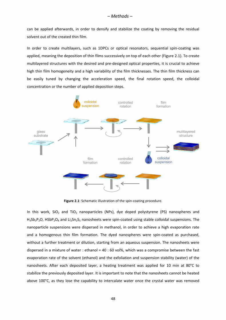
– Methods –
48
can be applied afterwards, in order to densify and stabilize the coating by removing the residual
solvent out of the created thin film.
In order to create multilayers, such as 1DPCs or optical resonators, sequential spin-coating was
applied, meaning the deposition of thin films successively on top of each other (Figure 2.1). To create
multilayered structures with the desired and pre-designed optical properties, it is crucial to achieve
high thin film homogeneity and a high variability of the film thicknesses. The thin film thickness can
be easily tuned by changing the acceleration speed, the final rotation speed, the colloidal
concentration or the number of applied deposition steps.
Figure 2.1: Schematic illustration of the spin-coating procedure.
In this work, SiO2 and TiO2 nanoparticles (NPs), dye doped polystyrene (PS) nanospheres and
H3Sb3P2O, HSbP2O8 and Li2Sn2S5 nanosheets were spin-coated using stable colloidal suspensions. The
nanoparticle suspensions were dispersed in methanol, in order to achieve a high evaporation rate
and a homogenous thin film formation. The dyed nanospheres were spin-coated as purchased,
without a further treatment or dilution, starting from an aqueous suspension. The nanosheets were
dispersed in a mixture of water : ethanol = 40 : 60 vol%, which was a compromise between the fast
evaporation rate of the solvent (ethanol) and the exfoliation and suspension stability (water) of the
nanosheets. After each deposited layer, a heating treatment was applied for 10 min at 80°C to
stabilize the previously deposited layer. It is important to note that the nanosheets cannot be heated
above 100°C, as they lose the capability to intercalate water once the crystal water was removed
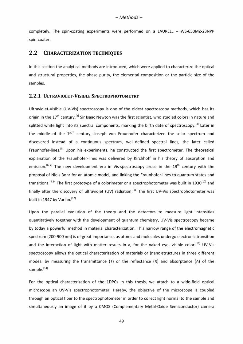
– Methods –
49
completely. The spin-coating experiments were performed on a LAURELL – WS-650MZ-23NPP
spin-coater.
2.2 CHARACTERIZATION TECHNIQUES
In this section the analytical methods are introduced, which were applied to characterize the optical
and structural properties, the phase purity, the elemental composition or the particle size of the
samples.
2.2.1 ULTRAVIOLET-VISIBLE SPECTROPHOTOMETRY
Ultraviolet-Visible (UV-Vis) spectroscopy is one of the oldest spectroscopy methods, which has its
origin in the 17th century.[3] Sir Isaac Newton was the first scientist, who studied colors in nature and
splitted white light into its spectral components, marking the birth date of spectroscopy.[4] Later in
the middle of the 19th century, Joseph von Fraunhofer characterized the solar spectrum and
discovered instead of a continuous spectrum, well-defined spectral lines, the later called
Fraunhofer-lines.[5] Upon his experiments, he constructed the first spectrometer. The theoretical
explanation of the Fraunhofer-lines was delivered by Kirchhoff in his theory of absorption and
emission.[6, 7] The new development era in Vis-spectroscopy arose in the 19th century with the
proposal of Niels Bohr for an atomic model, and linking the Fraunhofer-lines to quantum states and
transitions.[8, 9] The first prototype of a colorimeter or a spectrophotometer was built in 1930[10] and
finally after the discovery of ultraviolet (UV) radiation,[11] the first UV-Vis spectrophotometer was
built in 1947 by Varian.[12]
Upon the parallel evolution of the theory and the detectors to measure light intensities
quantitatively together with the development of quantum chemistry, UV-Vis spectroscopy became
by today a powerful method in material characterization. This narrow range of the electromagnetic
spectrum (200-900 nm) is of great importance, as atoms and molecules undergo electronic transition
and the interaction of light with matter results in a, for the naked eye, visible color.[13] UV-Vis
spectroscopy allows the optical characterization of materials or (nano)structures in three different
modes: by measuring the transmittance (T) or the reflectance (R) and absorptance (A) of the
sample.[14]
For the optical characterization of the 1DPCs in this thesis, we attach to a wide-field optical
microscope an UV-Vis spectrophotometer. Hereby, the objective of the microscope is coupled
through an optical fiber to the spectrophotometer in order to collect light normal to the sample and
simultaneously an image of it by a CMOS (Complementary Metal-Oxide Semiconductor) camera
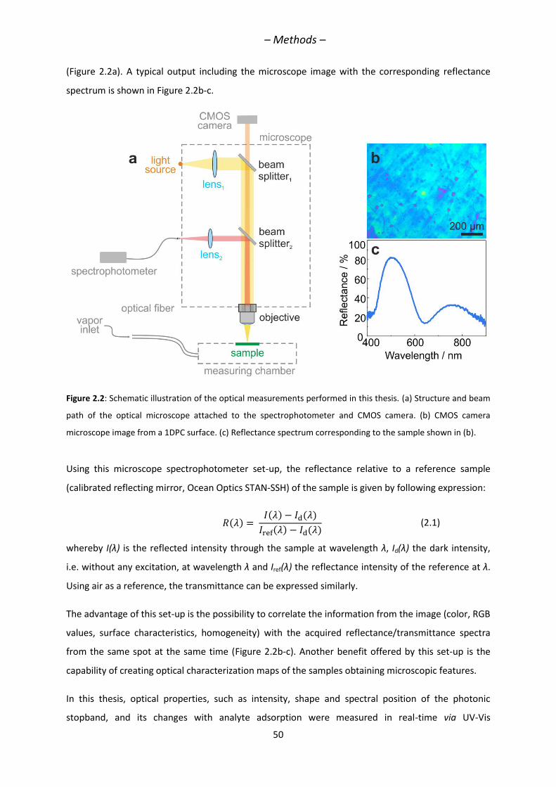
– Methods –
50
(Figure 2.2a). A typical output including the microscope image with the corresponding reflectance
spectrum is shown in Figure 2.2b-c.
Figure 2.2: Schematic illustration of the optical measurements performed in this thesis. (a) Structure and beam
path of the optical microscope attached to the spectrophotometer and CMOS camera. (b) CMOS camera
microscope image from a 1DPC surface. (c) Reflectance spectrum corresponding to the sample shown in (b).
Using this microscope spectrophotometer set-up, the reflectance relative to a reference sample
(calibrated reflecting mirror, Ocean Optics STAN-SSH) of the sample is given by following expression:
(2.1)
whereby I(λ) is the reflected intensity through the sample at wavelength λ, Id(λ) the dark intensity,
i.e. without any excitation, at wavelength λ and Iref(λ) the reflectance intensity of the reference at λ.
Using air as a reference, the transmittance can be expressed similarly.
The advantage of this set-up is the possibility to correlate the information from the image (color, RGB
values, surface characteristics, homogeneity) with the acquired reflectance/transmittance spectra
from the same spot at the same time (Figure 2.2b-c). Another benefit offered by this set-up is the
capability of creating optical characterization maps of the samples obtaining microscopic features.
In this thesis, optical properties, such as intensity, shape and spectral position of the photonic
stopband, and its changes with analyte adsorption were measured in real-time via UV-Vis
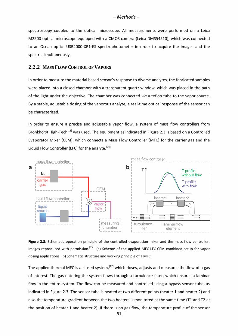
– Methods –
51
spectroscopy coupled to the optical microscope. All measurements were performed on a Leica
M2500 optical microscope equipped with a CMOS camera (Leica DMS54510), which was connected
to an Ocean optics USB4000-XR1-ES spectrophotometer in order to acquire the images and the
spectra simultaneously.
2.2.2 MASS FLOW CONTROL OF VAPORS
In order to measure the material based sensor`s response to diverse analytes, the fabricated samples
were placed into a closed chamber with a transparent quartz window, which was placed in the path
of the light under the objective. The chamber was connected via a teflon tube to the vapor source.
By a stable, adjustable dosing of the vaporous analyte, a real-time optical response of the sensor can
be characterized.
In order to ensure a precise and adjustable vapor flow, a system of mass flow controllers from
Bronkhorst High-Tech[15] was used. The equipment as indicated in Figure 2.3 is based on a Controlled
Evaporator Mixer (CEM), which connects a Mass Flow Controller (MFC) for the carrier gas and the
Liquid Flow Controller (LFC) for the analyte.[16]
Figure 2.3: Schematic operation principle of the controlled evaporation mixer and the mass flow controller.
Images reproduced with permission.[15]
(a) Scheme of the applied MFC-LFC-CEM combined setup for vapor
dosing applications. (b) Schematic structure and working principle of a MFC.
The applied thermal MFC is a closed system,[17] which doses, adjusts and measures the flow of a gas
of interest. The gas entering the system flows through a turbulence filter, which ensures a laminar
flow in the entire system. The flow can be measured and controlled using a bypass sensor tube, as
indicated in Figure 2.3. The sensor tube is heated at two different points (heater 1 and heater 2) and
also the temperature gradient between the two heaters is monitored at the same time (T1 and T2 at
the position of heater 1 and heater 2). If there is no gas flow, the temperature profile of the sensor
– Methods –
52
tube shows a Gaussian shape (green curve), and T1 and T2 are equal. By applying a gas flow, the gas
molecules are heated by heater 1 and the temperature gradient within the sensor tube is shifted
(blue curve), the two measured temperatures drift apart. The temperature profile shift and ΔT is
constant to the mass flow in the tube. The mass flow is controlled via a PID
(proportional-integral-derivative) controller and a valve at the end of the flow tube.
The LFC operates similarly to the MFC, using a sensor tube with a generated temperature difference.
However, hereby the main challenge is to design the components in a way that bubble formation and
retention is avoided. The third component, the CEM evaporates the liquid dosed by the LFC and
mixes it homogenously with the carrier gas, coming from the MFC.
In this thesis, the correct and stable dosing of diverse solvent vapors was crucial to determine the
sensor characteristics, most importantly the selectivity towards the main target, humidity, and to
prove the cross-selectivity to other analytes, such as alcohols, n-heptane, toluene or acetonitrile. The
set-up used in this thesis was calibrated for nitrogen with a maximum flow rate of 200 mL min-1 as a
carrier gas and water with a flow rate of maximum 2 g h-1 as an analyte. By applying different
analytes, the calculation tool of FLUIDAT on the Net software[18] was used. The CEM heater could
provide temperatures between ambient and 200°C.
2.2.3 SPECTROSCOPIC ELLIPSOMETRY
Ellipsometry has its roots in the end of the 19th century, as Paul Drude not only carried out the first
experimental studies on absorbing and transparent solids[19] but also derived the equations and with
this created the theoretical background of ellipsometry.[20] Later, Aspnes and Studna[21] performed
the first spectroscopic ellipsometry measurement by increasing the accuracy of the ellipsometric
measurements, after which wavelength-dependent measurements were possible. The first in situ
measurements were performed in 1984, as Muller and Farmer[22] succeeded to measure the entire
spectrum within a few seconds and with this allow following processes by this technique in real time.
Spectroscopic ellipsometry is a contactless, non-destructive method to determine thin film
properties, such as thickness, complex refractive index, roughness, composition or doping
concentration. Ellipsometry presents a fast and sensitive method, which is based on the
measurement of the changes of light polarization after reflection from the material.[23]
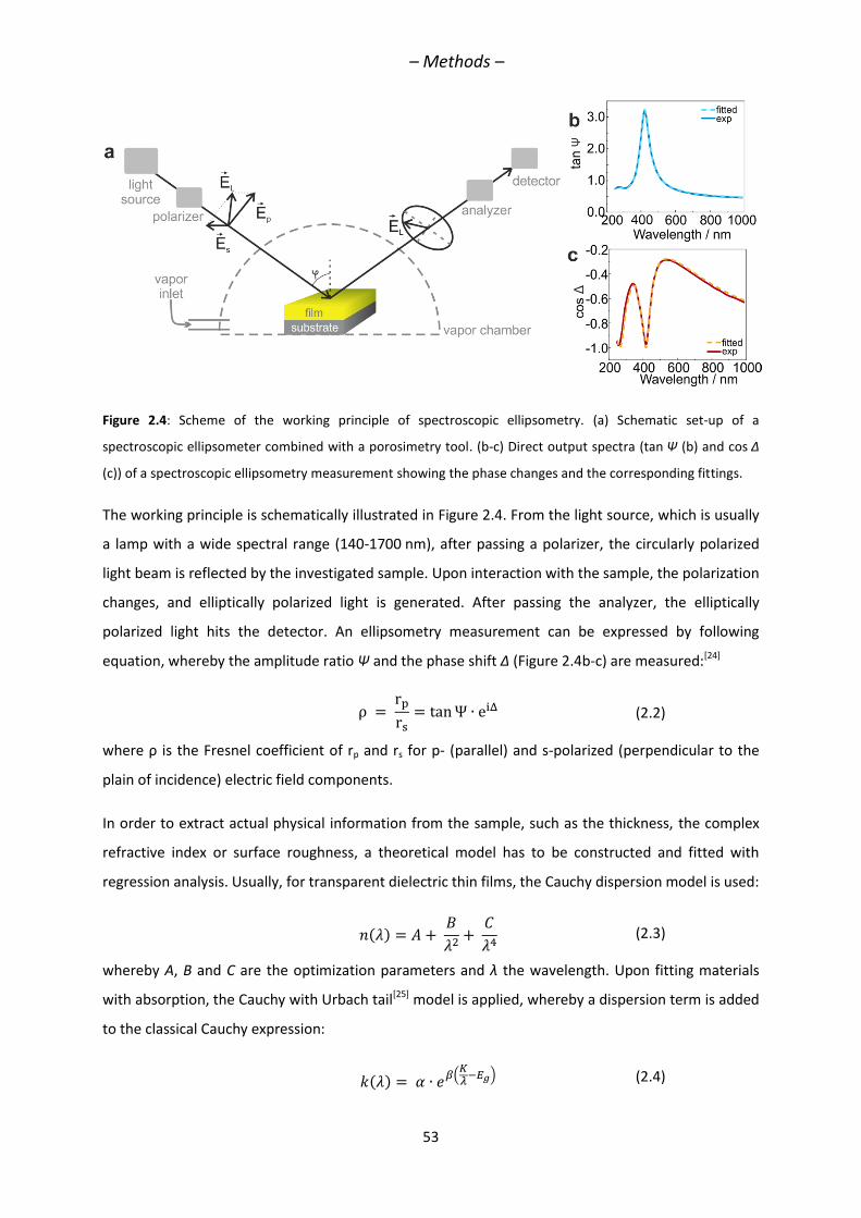
– Methods –
53
Figure 2.4: Scheme of the working principle of spectroscopic ellipsometry. (a) Schematic set-up of a
spectroscopic ellipsometer combined with a porosimetry tool. (b-c) Direct output spectra (tan Ψ (b) and cos Δ
(c)) of a spectroscopic ellipsometry measurement showing the phase changes and the corresponding fittings.
The working principle is schematically illustrated in Figure 2.4. From the light source, which is usually
a lamp with a wide spectral range (140-1700 nm), after passing a polarizer, the circularly polarized
light beam is reflected by the investigated sample. Upon interaction with the sample, the polarization
changes, and elliptically polarized light is generated. After passing the analyzer, the elliptically
polarized light hits the detector. An ellipsometry measurement can be expressed by following
equation, whereby the amplitude ratio Ψ and the phase shift Δ (Figure 2.4b-c) are measured:[24]
(2.2)
where ρ is the Fresnel coefficient of rp and rs for p- (parallel) and s-polarized (perpendicular to the
plain of incidence) electric field components.
In order to extract actual physical information from the sample, such as the thickness, the complex
refractive index or surface roughness, a theoretical model has to be constructed and fitted with
regression analysis. Usually, for transparent dielectric thin films, the Cauchy dispersion model is used:
(2.3)
whereby A, B and C are the optimization parameters and λ the wavelength. Upon fitting materials
with absorption, the Cauchy with Urbach tail[25] model is applied, whereby a dispersion term is added
to the classical Cauchy expression:
(2.4)
– Methods –
54
whereby α is the amplitude of the extinction coefficient, the exponent decay factor, Eg the optical
band gap and K the conversion constant between wavelength and energy units.
2.2.3.1 ELLIPSOMETRIC POROSIMETRY
Since the instrumental developments by Muller and Farmer[22] and later Kim, Collins and Verdam[26]
at the end of the 80s, ellipsometry is considered as a fast analytical method, which is capable of
process monitoring in situ and in real time. One example for such measurements is the monitoring of
vapor sorption in real-time on porous thin films.[27] In this thesis, a spectroscopic ellipsometer was
used, which was equipped with a vapor chamber (Figure 2.4), whereby different solvent vapors could
be dosed and injected to the chamber and the changes of the thin film materials are measured
instantaneously. Hereby again, the phase shift and the amplitude changes were measured
successively and with an automated model, optical isotherms monitoring the thickness and the
refractive index evolution with changing vapor pressure are created.
In this thesis, two different types of materials were investigated via spectroscopic ellipsometry: thin
films of porous materials (Figure 2.5a-b) and of two dimensional (2D) nanosheets (Figure 2.5c-d).
Both are capable of adsorbing vaporous analytes, such as water vapor or volatile organic compounds
(VOCs).
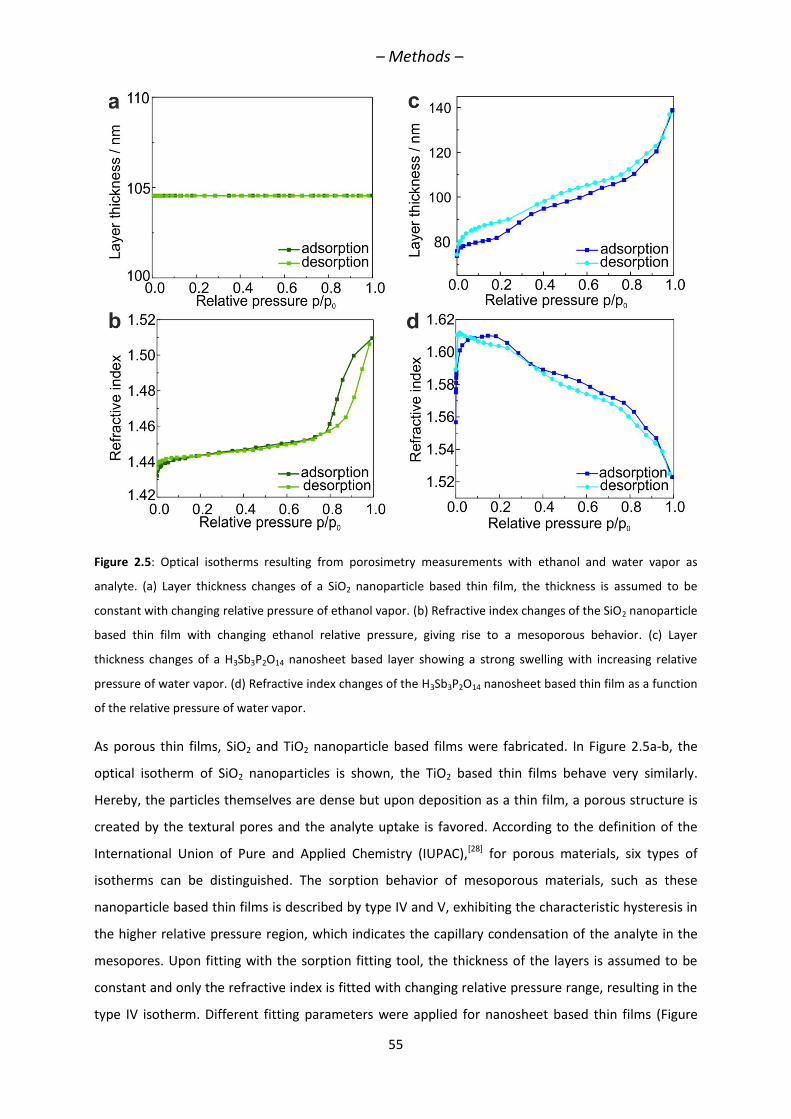
– Methods –
55
Figure 2.5: Optical isotherms resulting from porosimetry measurements with ethanol and water vapor as
analyte. (a) Layer thickness changes of a SiO2 nanoparticle based thin film, the thickness is assumed to be
constant with changing relative pressure of ethanol vapor. (b) Refractive index changes of the SiO2 nanoparticle
based thin film with changing ethanol relative pressure, giving rise to a mesoporous behavior. (c) Layer
thickness changes of a H3Sb3P2O14 nanosheet based layer showing a strong swelling with increasing relative
pressure of water vapor. (d) Refractive index changes of the H3Sb3P2O14 nanosheet based thin film as a function
of the relative pressure of water vapor.
As porous thin films, SiO2 and TiO2 nanoparticle based films were fabricated. In Figure 2.5a-b, the
optical isotherm of SiO2 nanoparticles is shown, the TiO2 based thin films behave very similarly.
Hereby, the particles themselves are dense but upon deposition as a thin film, a porous structure is
created by the textural pores and the analyte uptake is favored. According to the definition of the
International Union of Pure and Applied Chemistry (IUPAC),[28] for porous materials, six types of
isotherms can be distinguished. The sorption behavior of mesoporous materials, such as these
nanoparticle based thin films is described by type IV and V, exhibiting the characteristic hysteresis in
the higher relative pressure region, which indicates the capillary condensation of the analyte in the
mesopores. Upon fitting with the sorption fitting tool, the thickness of the layers is assumed to be
constant and only the refractive index is fitted with changing relative pressure range, resulting in the
type IV isotherm. Different fitting parameters were applied for nanosheet based thin films (Figure
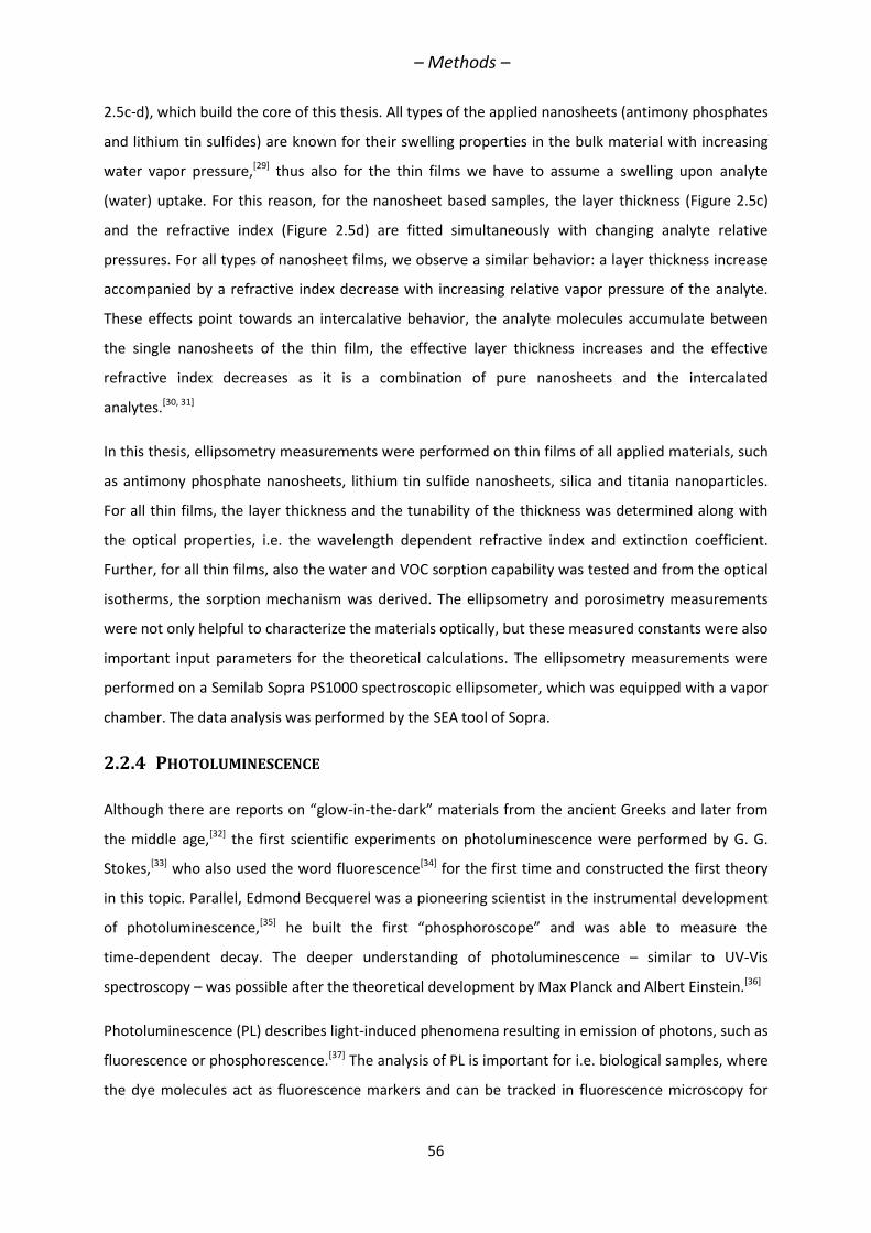
– Methods –
56
2.5c-d), which build the core of this thesis. All types of the applied nanosheets (antimony phosphates
and lithium tin sulfides) are known for their swelling properties in the bulk material with increasing
water vapor pressure,[29] thus also for the thin films we have to assume a swelling upon analyte
(water) uptake. For this reason, for the nanosheet based samples, the layer thickness (Figure 2.5c)
and the refractive index (Figure 2.5d) are fitted simultaneously with changing analyte relative
pressures. For all types of nanosheet films, we observe a similar behavior: a layer thickness increase
accompanied by a refractive index decrease with increasing relative vapor pressure of the analyte.
These effects point towards an intercalative behavior, the analyte molecules accumulate between
the single nanosheets of the thin film, the effective layer thickness increases and the effective
refractive index decreases as it is a combination of pure nanosheets and the intercalated
analytes.[30, 31]
In this thesis, ellipsometry measurements were performed on thin films of all applied materials, such
as antimony phosphate nanosheets, lithium tin sulfide nanosheets, silica and titania nanoparticles.
For all thin films, the layer thickness and the tunability of the thickness was determined along with
the optical properties, i.e. the wavelength dependent refractive index and extinction coefficient.
Further, for all thin films, also the water and VOC sorption capability was tested and from the optical
isotherms, the sorption mechanism was derived. The ellipsometry and porosimetry measurements
were not only helpful to characterize the materials optically, but these measured constants were also
important input parameters for the theoretical calculations. The ellipsometry measurements were
performed on a Semilab Sopra PS1000 spectroscopic ellipsometer, which was equipped with a vapor
chamber. The data analysis was performed by the SEA tool of Sopra.
2.2.4 PHOTOLUMINESCENCE
Although there are reports on “glow-in-the-dark” materials from the ancient Greeks and later from
the middle age,[32] the first scientific experiments on photoluminescence were performed by G. G.
Stokes,[33] who also used the word fluorescence[34] for the first time and constructed the first theory
in this topic. Parallel, Edmond Becquerel was a pioneering scientist in the instrumental development
of photoluminescence,[35] he built the first “phosphoroscope” and was able to measure the
time-dependent decay. The deeper understanding of photoluminescence – similar to UV-Vis
spectroscopy – was possible after the theoretical development by Max Planck and Albert Einstein.[36]
Photoluminescence (PL) describes light-induced phenomena resulting in emission of photons, such as
fluorescence or phosphorescence.[37] The analysis of PL is important for i.e. biological samples, where
the dye molecules act as fluorescence markers and can be tracked in fluorescence microscopy for
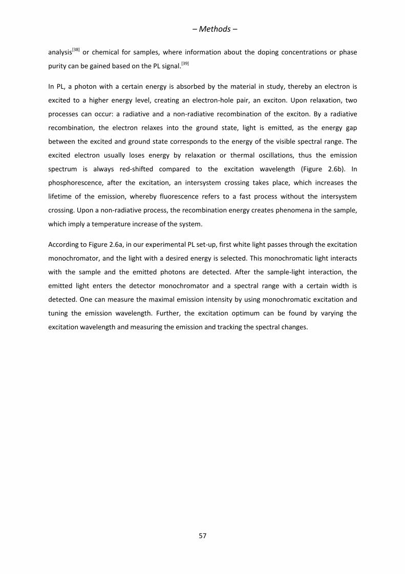
– Methods –
57
analysis[38] or chemical for samples, where information about the doping concentrations or phase
purity can be gained based on the PL signal.[39]
In PL, a photon with a certain energy is absorbed by the material in study, thereby an electron is
excited to a higher energy level, creating an electron-hole pair, an exciton. Upon relaxation, two
processes can occur: a radiative and a non-radiative recombination of the exciton. By a radiative
recombination, the electron relaxes into the ground state, light is emitted, as the energy gap
between the excited and ground state corresponds to the energy of the visible spectral range. The
excited electron usually loses energy by relaxation or thermal oscillations, thus the emission
spectrum is always red-shifted compared to the excitation wavelength (Figure 2.6b). In
phosphorescence, after the excitation, an intersystem crossing takes place, which increases the
lifetime of the emission, whereby fluorescence refers to a fast process without the intersystem
crossing. Upon a non-radiative process, the recombination energy creates phenomena in the sample,
which imply a temperature increase of the system.
According to Figure 2.6a, in our experimental PL set-up, first white light passes through the excitation
monochromator, and the light with a desired energy is selected. This monochromatic light interacts
with the sample and the emitted photons are detected. After the sample-light interaction, the
emitted light enters the detector monochromator and a spectral range with a certain width is
detected. One can measure the maximal emission intensity by using monochromatic excitation and
tuning the emission wavelength. Further, the excitation optimum can be found by varying the
excitation wavelength and measuring the emission and tracking the spectral changes.
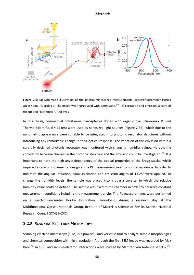
– Methods –
58
Figure 2.6: (a) Schematic illustration of the photoluminescence measurements, spectrofluorometer Horiba
Jobin-Ybon, Fluorolog-3. The image was reproduced with permission.[40]
(b) Excitation and emission spectra of
the utilized Fluoromax R, Red dyes.
In this thesis, commercial polystyrene nanospheres doped with organic dye (Fluoromax R, Red
Thermo Scientific, d ≈ 25 nm) were used as nanosized light sources (Figure 2.6b), which due to the
nanometric appearance were suitable to be integrated into photonic resonator structures without
introducing any remarkable change in their optical response. The variation of the emission within a
carefully designed photonic resonator was monitored with changing humidity values. Hereby, the
correlation between changes in the photonic structure and the emission could be investigated.[41] It is
important to note the high angle-dependency of the optical properties of the Bragg stacks, which
required a careful instrumental design and a PL measurement near to normal incidence. In order to
minimize the angular influence, equal excitation and emission angles of 11.25° were applied. To
change the humidity levels, the sample was placed into a quartz cuvette, in which the relative
humidity value could be defined. The sample was fixed to the chamber in order to preserve constant
measurement conditions including the measurement angle. The PL measurements were performed
on a spectrofluorometer Horiba Jobin-Ybon, Fluorolog-3, during a research stay at the
Multifunctional Optical Materials Group, Institute of Materials Science of Seville, Spanish National
Research Council (ICMSE-CSIC).
2.2.5 SCANNING ELECTRON MICROSCOPY
Scanning electron microscopy (SEM) is a powerful and versatile tool to analyze sample morphologies
and chemical composition with high resolution. Although the first SEM image was recorded by Max
Knoll[42] in 1935 and sample-electron interactions were studied by Manfred von Ardenne in 1937,[43]
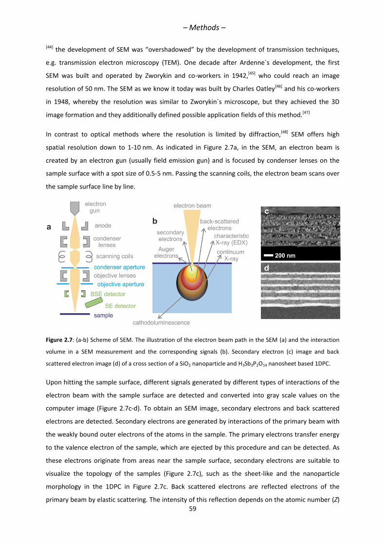
– Methods –
59
[44] the development of SEM was “overshadowed” by the development of transmission techniques,
e.g. transmission electron microscopy (TEM). One decade after Ardenne`s development, the first
SEM was built and operated by Zworykin and co-workers in 1942,[45] who could reach an image
resolution of 50 nm. The SEM as we know it today was built by Charles Oatley[46] and his co-workers
in 1948, whereby the resolution was similar to Zworykin`s microscope, but they achieved the 3D
image formation and they additionally defined possible application fields of this method.[47]
In contrast to optical methods where the resolution is limited by diffraction,[48] SEM offers high
spatial resolution down to 1-10 nm. As indicated in Figure 2.7a, in the SEM, an electron beam is
created by an electron gun (usually field emission gun) and is focused by condenser lenses on the
sample surface with a spot size of 0.5-5 nm. Passing the scanning coils, the electron beam scans over
the sample surface line by line.
Figure 2.7: (a-b) Scheme of SEM. The illustration of the electron beam path in the SEM (a) and the interaction
volume in a SEM measurement and the corresponding signals (b). Secondary electron (c) image and back
scattered electron image (d) of a cross section of a SiO2 nanoparticle and H3Sb3P2O14 nanosheet based 1DPC.
Upon hitting the sample surface, different signals generated by different types of interactions of the
electron beam with the sample surface are detected and converted into gray scale values on the
computer image (Figure 2.7c-d). To obtain an SEM image, secondary electrons and back scattered
electrons are detected. Secondary electrons are generated by interactions of the primary beam with
the weakly bound outer electrons of the atoms in the sample. The primary electrons transfer energy
to the valence electron of the sample, which are ejected by this procedure and can be detected. As
these electrons originate from areas near the sample surface, secondary electrons are suitable to
visualize the topology of the samples (Figure 2.7c), such as the sheet-like and the nanoparticle
morphology in the 1DPC in Figure 2.7c. Back scattered electrons are reflected electrons of the
primary beam by elastic scattering. The intensity of this reflection depends on the atomic number (Z)
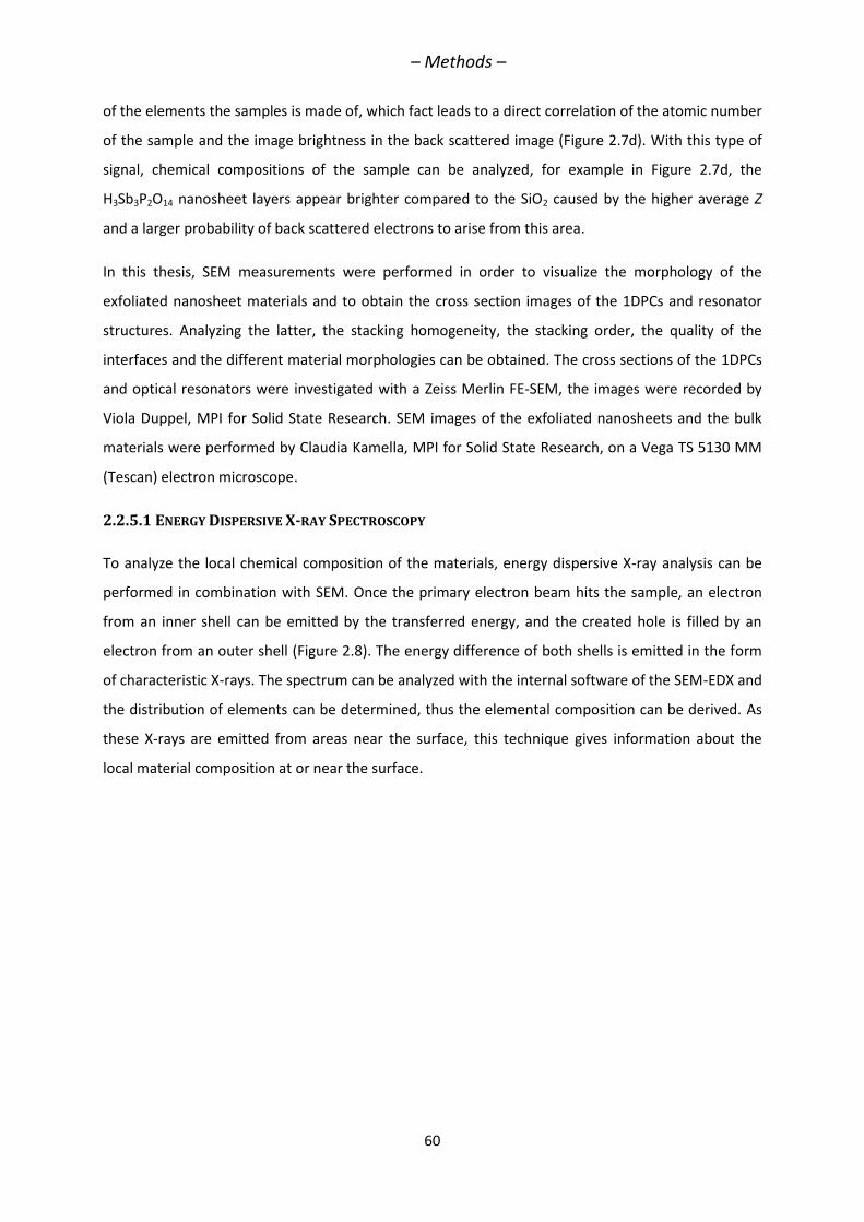
– Methods –
60
of the elements the samples is made of, which fact leads to a direct correlation of the atomic number
of the sample and the image brightness in the back scattered image (Figure 2.7d). With this type of
signal, chemical compositions of the sample can be analyzed, for example in Figure 2.7d, the
H3Sb3P2O14 nanosheet layers appear brighter compared to the SiO2 caused by the higher average Z
and a larger probability of back scattered electrons to arise from this area.
In this thesis, SEM measurements were performed in order to visualize the morphology of the
exfoliated nanosheet materials and to obtain the cross section images of the 1DPCs and resonator
structures. Analyzing the latter, the stacking homogeneity, the stacking order, the quality of the
interfaces and the different material morphologies can be obtained. The cross sections of the 1DPCs
and optical resonators were investigated with a Zeiss Merlin FE-SEM, the images were recorded by
Viola Duppel, MPI for Solid State Research. SEM images of the exfoliated nanosheets and the bulk
materials were performed by Claudia Kamella, MPI for Solid State Research, on a Vega TS 5130 MM
(Tescan) electron microscope.
2.2.5.1 ENERGY DISPERSIVE X-RAY SPECTROSCOPY
To analyze the local chemical composition of the materials, energy dispersive X-ray analysis can be
performed in combination with SEM. Once the primary electron beam hits the sample, an electron
from an inner shell can be emitted by the transferred energy, and the created hole is filled by an
electron from an outer shell (Figure 2.8). The energy difference of both shells is emitted in the form
of characteristic X-rays. The spectrum can be analyzed with the internal software of the SEM-EDX and
the distribution of elements can be determined, thus the elemental composition can be derived. As
these X-rays are emitted from areas near the surface, this technique gives information about the
local material composition at or near the surface.
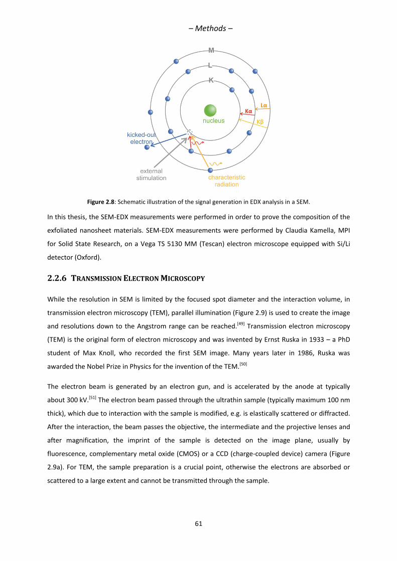
– Methods –
61
Figure 2.8: Schematic illustration of the signal generation in EDX analysis in a SEM.
In this thesis, the SEM-EDX measurements were performed in order to prove the composition of the
exfoliated nanosheet materials. SEM-EDX measurements were performed by Claudia Kamella, MPI
for Solid State Research, on a Vega TS 5130 MM (Tescan) electron microscope equipped with Si/Li
detector (Oxford).
2.2.6 TRANSMISSION ELECTRON MICROSCOPY
While the resolution in SEM is limited by the focused spot diameter and the interaction volume, in
transmission electron microscopy (TEM), parallel illumination (Figure 2.9) is used to create the image
and resolutions down to the Angstrom range can be reached.[49] Transmission electron microscopy
(TEM) is the original form of electron microscopy and was invented by Ernst Ruska in 1933 – a PhD
student of Max Knoll, who recorded the first SEM image. Many years later in 1986, Ruska was
awarded the Nobel Prize in Physics for the invention of the TEM.[50]
The electron beam is generated by an electron gun, and is accelerated by the anode at typically
about 300 kV.[51] The electron beam passed through the ultrathin sample (typically maximum 100 nm
thick), which due to interaction with the sample is modified, e.g. is elastically scattered or diffracted.
After the interaction, the beam passes the objective, the intermediate and the projective lenses and
after magnification, the imprint of the sample is detected on the image plane, usually by
fluorescence, complementary metal oxide (CMOS) or a CCD (charge-coupled device) camera (Figure
2.9a). For TEM, the sample preparation is a crucial point, otherwise the electrons are absorbed or
scattered to a large extent and cannot be transmitted through the sample.
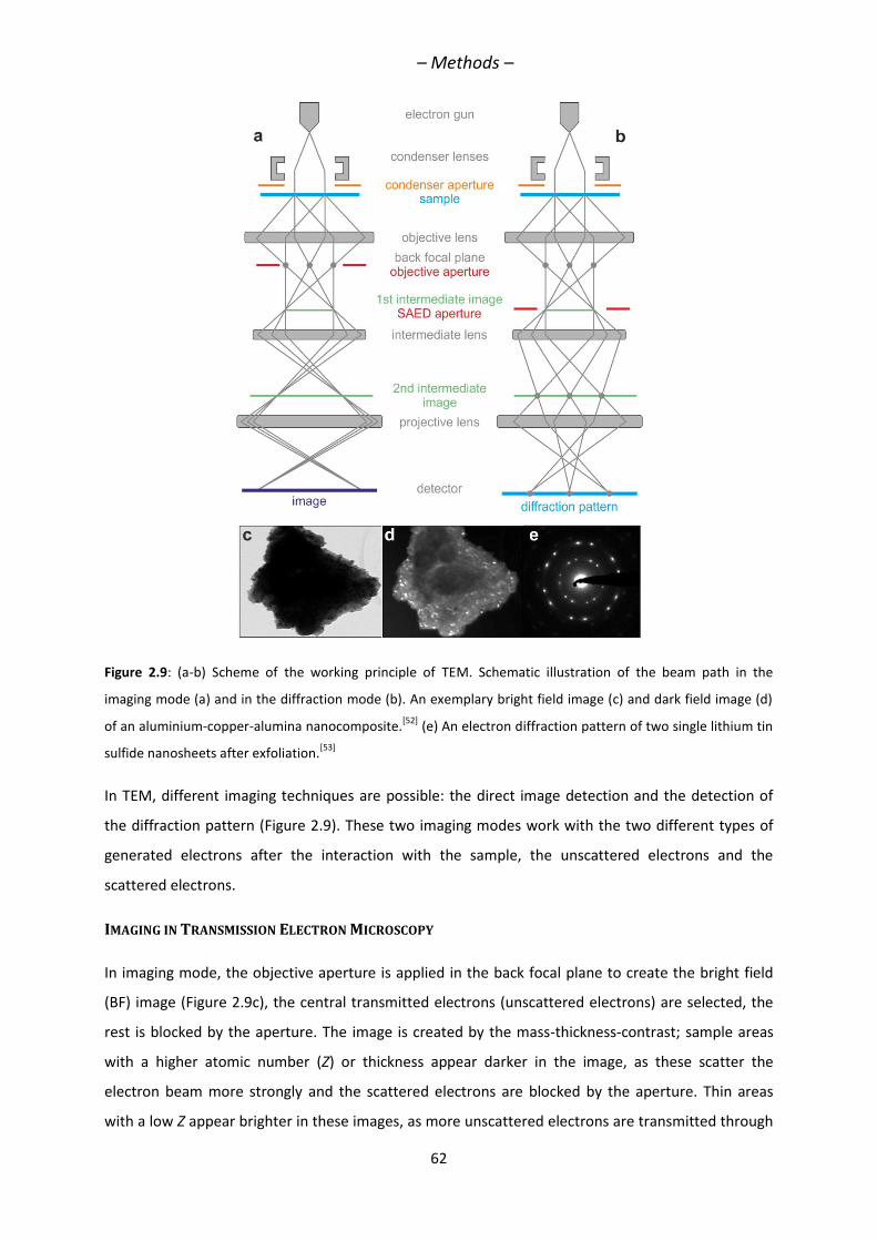
– Methods –
62
Figure 2.9: (a-b) Scheme of the working principle of TEM. Schematic illustration of the beam path in the
imaging mode (a) and in the diffraction mode (b). An exemplary bright field image (c) and dark field image (d)
of an aluminium-copper-alumina nanocomposite.[52]
(e) An electron diffraction pattern of two single lithium tin
sulfide nanosheets after exfoliation.[53]
In TEM, different imaging techniques are possible: the direct image detection and the detection of
the diffraction pattern (Figure 2.9). These two imaging modes work with the two different types of
generated electrons after the interaction with the sample, the unscattered electrons and the
scattered electrons.
IMAGING IN TRANSMISSION ELECTRON MICROSCOPY
In imaging mode, the objective aperture is applied in the back focal plane to create the bright field
(BF) image (Figure 2.9c), the central transmitted electrons (unscattered electrons) are selected, the
rest is blocked by the aperture. The image is created by the mass-thickness-contrast; sample areas
with a higher atomic number (Z) or thickness appear darker in the image, as these scatter the
electron beam more strongly and the scattered electrons are blocked by the aperture. Thin areas
with a low Z appear brighter in these images, as more unscattered electrons are transmitted through
– Methods –
63
the sample and reach the detector. By blocking the unscattered electrons and using the scattered
electrons in the imaging mode, the dark field (DF) image (Figure 2.9d) is created. Hereby sample
areas with a higher Z appear brighter (e.g. clusters in the composite with a larger Z, embedded in a
lower Z matrix), as more electrons from these areas are detected, as only the scattered electrons are
used for the image formation.
ELECTRON DIFFRACTION IN TRANSMISSION ELECTRON MICROSCOPY
Another powerful tool of TEM in the analysis of crystalline samples is the selected area electron
diffraction (SAED) analysis. The thin crystalline sample in TEM acts to the incident electron beam as a
diffraction grating, and the electrons get diffracted by the atoms of the sample. In this technique, the
SAED aperture is inserted and the back focal plane is projected, and as a result, a diffraction pattern
arises (Figure 2.9e). The SAED aperture gives additionally the possibility to select the sample area and
record the diffraction pattern from this region. From the diffraction pattern, information on the
crystal structure, composition or phase purity can be gained.
SCANNING TRANSMISSION ELECTRON MICROSCOPY
TEM can be modified with the application of a scanning coil and additional lenses to a scanning TEM
(STEM). In contrary to parallel illumination of the sample, the electron beam is focused and scanned
above the sample surface. In STEM, the image is formed by detecting the counts, the amount of
detected electrons arising from the different points of the sample.
2.2.6.1 ELECTRON ENERGY LOSS SPECTROSCOPY
In combination with STEM, in addition to the visualization of the sample with high resolution, the
local composition and the chemical properties can also be analyzed with Electron Energy Loss
Spectroscopy (EELS).[54, 55] Upon passing the specimen, the electron beam interacts with the sample
and the electrons are scattered elastically or inelastically. Inelastic scattering refers to electrons
which lose from their original energy upon, while the energy of elastically scattered ones remains
constant. These scattered electrons can be split up by a magnetic prism (Figure 2.10a), which deflects
the electron beam depending on its energy. With this, the exact energy losses can be determined
and the material composition can be analyzed. In the EEL spectrum, three different regions can be
distinguished. The zero loss peak (ZLP) appears at 0 eV energy loss, and refers to electrons which do
not undergo inelastic scattering, but are only scattered elastically and do not lose energy. The ZLP is
usually used for the sample calibration. Secondly, the low loss range (energy loss 2-50 eV) represents
the excitation of plasmons, inter- or intraband transitions. This region can be used for phase
identification, or the analysis of bandgaps. The third and for this thesis the most important range is
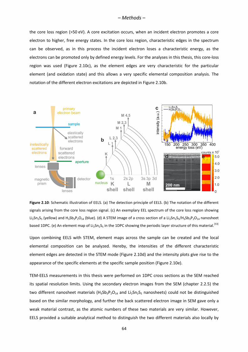
– Methods –
64
the core loss region (>50 eV). A core excitation occurs, when an incident electron promotes a core
electron to higher, free energy states. In the core loss region, characteristic edges in the spectrum
can be observed, as in this process the incident electron loses a characteristic energy, as the
electrons can be promoted only by defined energy levels. For the analyses in this thesis, this core-loss
region was used (Figure 2.10c), as the element edges are very characteristic for the particular
element (and oxidation state) and this allows a very specific elemental composition analysis. The
notation of the different electron excitations are depicted in Figure 2.10b.
Figure 2.10: Schematic illustration of EELS. (a) The detection principle of EELS. (b) The notation of the different
signals arising from the core loss region signal. (c) An exemplary EEL spectrum of the core loss region showing
Li2Sn2S5 (yellow) and H3Sb3P2O14 (blue). (d) A STEM image of a cross section of a Li2Sn2S5/H3Sb3P2O14 nanosheet
based 1DPC. (e) An element map of Li2Sn2S5 in the 1DPC showing the periodic layer structure of this material.[53]
Upon combining EELS with STEM, element maps across the sample can be created and the local
elemental composition can be analyzed. Hereby, the intensities of the different characteristic
element edges are detected in the STEM mode (Figure 2.10d) and the intensity plots give rise to the
appearance of the specific elements at the specific sample position (Figure 2.10e).
TEM-EELS measurements in this thesis were performed on 1DPC cross sections as the SEM reached
its spatial resolution limits. Using the secondary electron images from the SEM (chapter 2.2.5) the
two different nanosheet materials (H3Sb3P2O14 and Li2Sn2S5 nanosheets) could not be distinguished
based on the similar morphology, and further the back scattered electron image in SEM gave only a
weak material contrast, as the atomic numbers of these two materials are very similar. However,
EELS provided a suitable analytical method to distinguish the two different materials also locally by
– Methods –
65
performing the elemental mapping. Further, in this thesis TEM-SAED patterns were recorded in order
to prove the turbostratically disordered morphology (rotated along the z-direction) of the
nanosheets after the exfoliation of the bulk material.
TEM and EELS measurements were performed by Dr. Sophia Betzler, LMU München and MPI for
Solid State Research, on a FEI Titan Themis microscope (60–300 kV) equipped with a Cs corrector.
TEM measurements with SAED patterns were measured by Viola Duppel, MPI for Solid State
Research, on a Phillips CM30 ST TEM (300 kV, LaB6 cathode) equipped with a Gatan CCD camera.
2.2.7 X-RAY DIFFRACTION
X-ray diffraction (XRD) is a powerful and non-destructive method to analyze and identify crystalline
samples regarding their crystal structure, crystallinity, phase purity and particle size. X-rays, also
called Röntgen-rays, were discovered by Wilhelm Röntgen in 1895, for which he was awarded with
the first Nobel Prize in Physics in 1901.[56] Long time ago it was debated by the physical society,
whether X-rays are electromagnetic waves. The final prove was delivered by Max von Laue by his
diffraction experiment of X-rays on a copper sulfide crystal in 1912 at the University of Munich, for
which he was awarded with the Nobel Prize in 1914.[57] This ultimately proved the wave-nature of X-
rays and simultaneously delivered important contributions to crystal structure analysis via X-rays.
After Laue`s discovery, many scientists were involved in the theoretical and instrumental
development of X-ray crystallography, whereby the most important contribution was provided by
William Henry Bragg and his son William Lawrence Bragg, who were awarded for “their services in
the analysis of crystal structure by means of X-rays”, including the Bragg law, with the Nobel Prize in
1915.[58]
Similar to other analytical techniques, also in XRD analysis the probe beam must have a wavelength
comparable to the range of the analyzed specimen features, i.e. the atomic spacings in the crystal
structure. For this, X-rays are generated when targets, such as Cu or Mo, are irradiated by
high-energy electrons under vacuum. Thereby, core electrons are promoted to higher levels of outer
shells, and by the relaxation back to the ground state, they emit X-rays with a characteristic
wavelength (λ (Cu-Kα) = 1.541 Å, λ (Mo-Kα) = 0.710 Å). The created X-ray beam passes through a
monochromator and a collimator before interacting with the crystalline sample. The incident
monochromatic X-ray beam is diffracted at the lattice planes of the sample (Figure 2.11a) and
intensity maxima arise from constructive interferences, when the Bragg equation (2.5) is fulfilled:
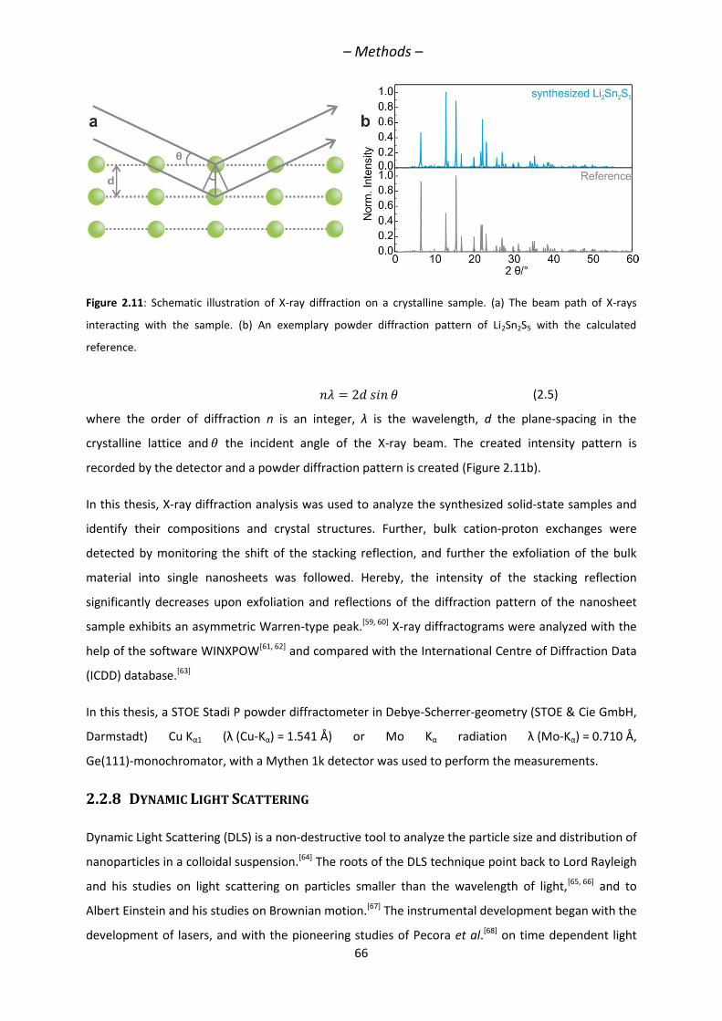
– Methods –
66
Figure 2.11: Schematic illustration of X-ray diffraction on a crystalline sample. (a) The beam path of X-rays
interacting with the sample. (b) An exemplary powder diffraction pattern of Li2Sn2S5 with the calculated
reference.
(2.5)
where the order of diffraction n is an integer, λ is the wavelength, d the plane-spacing in the
crystalline lattice and the incident angle of the X-ray beam. The created intensity pattern is
recorded by the detector and a powder diffraction pattern is created (Figure 2.11b).
In this thesis, X-ray diffraction analysis was used to analyze the synthesized solid-state samples and
identify their compositions and crystal structures. Further, bulk cation-proton exchanges were
detected by monitoring the shift of the stacking reflection, and further the exfoliation of the bulk
material into single nanosheets was followed. Hereby, the intensity of the stacking reflection
significantly decreases upon exfoliation and reflections of the diffraction pattern of the nanosheet
sample exhibits an asymmetric Warren-type peak.[59, 60] X-ray diffractograms were analyzed with the
help of the software WINXPOW[61, 62] and compared with the International Centre of Diffraction Data
(ICDD) database.[63]
In this thesis, a STOE Stadi P powder diffractometer in Debye-Scherrer-geometry (STOE & Cie GmbH,
Darmstadt) Cu Kα1 (λ (Cu-Kα) = 1.541 Å) or Mo Kα radiation λ (Mo-Kα) = 0.710 Å,
Ge(111)-monochromator, with a Mythen 1k detector was used to perform the measurements.
2.2.8 DYNAMIC LIGHT SCATTERING
Dynamic Light Scattering (DLS) is a non-destructive tool to analyze the particle size and distribution of
nanoparticles in a colloidal suspension.[64] The roots of the DLS technique point back to Lord Rayleigh
and his studies on light scattering on particles smaller than the wavelength of light,[65, 66] and to
Albert Einstein and his studies on Brownian motion.[67] The instrumental development began with the
development of lasers, and with the pioneering studies of Pecora et al.[68] on time dependent light
– Methods –
67
scattering. At that time, DLS was used to measure the diffusion of macromolecules and to calculate
the hydrodynamic radius. With the development of information technology, for today, DLS became a
fast method to analyze particle size and size distribution in solution.
In a DLS measurement, a monochromatic laser beam travels through the measured suspension. The
sample is thermally stabilized, in order to keep the thermal motion constant, which influences the
Brownian motion in the suspension, as it has an important impact on the particle size determination.
Upon illuminating the sample, the suspended particles scatter the laser light. The intensity variations
caused by interference of the scattered light by the moving particles give rise to the diffusion
coefficient and hence the size of the suspended particles, according to the Einstein-Stokes equation
(2.6):
(2.6)
where D is the diffusion coefficient, kB the Boltzmann constant, T the temperature, the viscosity
and d the hydrodynamic diameter of the particles. For the exact determination of the particle size in
DLS, requirement is that the particles are in a size range approx. below 1 micron.
In this thesis, DLS measurements were performed in order to measure the particle size of the applied
TiO2 and SiO2 nanoparticles after the synthesis. The measurements were performed with a Malvern
Zetasizer Nano-ZS with a 4 mW He-Ne laser (= 633 nm).
2.2.9 ATOMIC FORCE MICROSCOPY
Atomic Force Microscopy (AFM) is a type of Scanning Probe Microscopy (SPM),[69] which is capable of
investigating the surface of nanostructured samples with a high resolution. Scanning Tunneling
Microscopy (STM), as a predecessor of AFM, was invented by Gerd Binnig and Heinrich Rohrer in the
early 1980s, and the two inventors were awarded with the Nobel Prize for Physics in 1986 (together
with Ernst Ruska for the development of TEM).[70] Few years later, AFM and its first implementations
were developed by Gerd Binning and co-workers.[71, 72]
AFM can be used in three modes: for force measurement, for manipulation or for imaging. In this
thesis, only the latter, the imaging mode was used and, hence, will be discussed here in detail. In
AFM, a sharp probe tip, fixed on a flexible cantilever, is brought in contact with the sample and scans
through the sample surface.[73] By experiencing the sample`s height variations, the cantilever is
deflected in order to follow the sample surface with the tip. Further, a laser beam is reflected on the
back side of the cantilever and hits a photodiode, which can read out the position of the laser beam.
– Methods –
68
By the deflection of the cantilever, the laser beam is also deflected and its position on the
photodiode is changed. After scanning the sample surface line by line, a 3D image can be created,
which corresponds to the topology of the sample. To avoid damages of the surface, often the tapping
mode is used, whereby the tip is continuously oscillating and does not touch the sample. By
monitoring the changes in this oscillation, a height profile can be reconstructed similar to the contact
mode. AFM is a very sensitive technique to surface variations and shows a height resolution below
1 nm.[74]
In this work, this technique was used to determine, if the exfoliation of the bulk material into
nanosheets was successful and if single or multilayered nanosheets were achieved by the
delamination. The measurements were conducted by Pirmin Ganter, MPI for Solid State Research, on
a Veeco CP II system.
2.2.10 IMPEDANCE SPECTROSCOPY
Impedance spectroscopy or dielectric spectroscopy is a method to analyze the dielectric properties of
samples as a function of the frequency. An alternating current (AC) flows through the sample and
interacts with the dipole moments. At different AC frequencies, various dielectric processes are
generated and measured. The following processes can occur with decreasing AC frequency ranges:
electronic polarization, atomic polarization, dipole relaxation, ionic relaxation or dielectric relaxation.
Depending on the nature of the measured sample, different processes dominate, but the sum of all
processes is measured as the impedance. The characteristic features can be analyzed indirectly by
fitting the electric response of a model circuit with different components, such as capacitors or
resistance in parallel or series connection. With the combination of the basic circuit elements, even
complex structures can be described, such as ionic conductors as a capacitor and a resistance
connected in parallel.
In this thesis, the conductance change of the nanosheet thin films at various relative humidity levels
was measured in a two-point measurement geometry. An AC voltage of 500 mV was applied to the
sample and the frequency range of 1 Hz to 1 MHz measured, however for time-dependent
measurements, the frequency was fixed to 300 Hz and the conductance was measured. The
measurements were performed by Pirmin Ganter, MPI for Solid State Research, on a Princeton
Applied Research, Versa STAT MC impedance bridge.
2.3 THEORETICAL CALCULATIONS
Theoretical calculations were performed in order to design the photonic structures prior to
fabrication, to understand the optical properties (reflectance, transmittance, field intensity
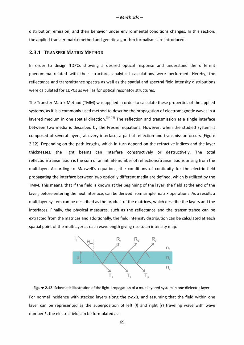
– Methods –
69
distribution, emission) and their behavior under environmental conditions changes. In this section,
the applied transfer matrix method and genetic algorithm formalisms are introduced.
2.3.1 TRANSFER MATRIX METHOD
In order to design 1DPCs showing a desired optical response and understand the different
phenomena related with their structure, analytical calculations were performed. Hereby, the
reflectance and transmittance spectra as well as the spatial and spectral field intensity distributions
were calculated for 1DPCs as well as for optical resonator structures.
The Transfer Matrix Method (TMM) was applied in order to calculate these properties of the applied
systems, as it is a commonly used method to describe the propagation of electromagnetic waves in a
layered medium in one spatial direction.[75, 76] The reflection and transmission at a single interface
between two media is described by the Fresnel equations. However, when the studied system is
composed of several layers, at every interface, a partial reflection and transmission occurs (Figure
2.12). Depending on the path lengths, which in turn depend on the refractive indices and the layer
thicknesses, the light beams can interfere constructively or destructively. The total
reflection/transmission is the sum of an infinite number of reflections/transmissions arising from the
multilayer. According to Maxwell`s equations, the conditions of continuity for the electric field
propagating the interface between two optically different media are defined, which is utilized by the
TMM. This means, that if the field is known at the beginning of the layer, the field at the end of the
layer, before entering the next interface, can be derived from simple matrix operations. As a result, a
multilayer system can be described as the product of the matrices, which describe the layers and the
interfaces. Finally, the physical measures, such as the reflectance and the transmittance can be
extracted from the matrices and additionally, the field intensity distribution can be calculated at each
spatial point of the multilayer at each wavelength giving rise to an intensity map.
Figure 2.12: Schematic illustration of the light propagation of a multilayered system in one dielectric layer.
For normal incidence with stacked layers along the z-axis, and assuming that the field within one
layer can be represented as the superposition of left (l) and right (r) traveling wave with wave
number k, the electric field can be formulated as:
– Methods –
70
(2.7)
The field gradient F(z) can be expressed as the derivative of E(z):
(2.8)
According to Maxwell`s equations, E and F must be continuous across a boundary, whereby one can
express the field as a vector of (E(z), (z)).
A propagation of light in the multilayered structure over a distance d into a positive z direction can be
described by the matrix in (2.9):
(2.9)
Using this, we can express the field at point z+d as:
(2.10)
whereby k is the wave number in the medium and d the layer thickness. For a system with N layers,
the system transfer matrix Ms is a product of all matrices. With this, at all points of the structure, by
applying the according matrix, the field can be calculated.
The main goal of these calculations is to extract the reflectance and transmittance after the
interaction with light. Assuming the multilayer starts at z = 0, the reflectance can be calculated for
negative z values and the transmission for z > d´ values, where d´ corresponds to the total thickness:
(2.11)
(2.12)
whereby r and t are the amplitude of the reflectance and transmittance coefficients, kl and kr the
wave numbers in the medium of the left (l) and right (r) propagating light waves. Finally, the
transmittance and the reflectance values are given by equations (2.13 and 2.14):
(2.13)
and
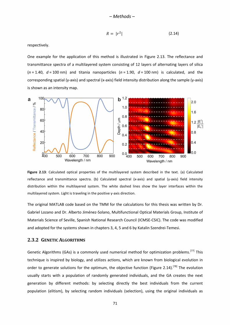
– Methods –
71
(2.14)
respectively.
One example for the application of this method is illustrated in Figure 2.13. The reflectance and
transmittance spectra of a multilayered system consisting of 12 layers of alternating layers of silica
(n = 1.40, d = 100 nm) and titania nanoparticles (n = 1.90, d = 100 nm) is calculated, and the
corresponding spatial (y-axis) and spectral (x-axis) field intensity distribution along the sample (y-axis)
is shown as an intensity map.
Figure 2.13: Calculated optical properties of the multilayered system described in the text. (a) Calculated
reflectance and transmittance spectra. (b) Calculated spectral (x-axis) and spatial (y-axis) field intensity
distribution within the multilayered system. The white dashed lines show the layer interfaces within the
multilayered system. Light is traveling in the positive y-axis direction.
The original MATLAB code based on the TMM for the calculations for this thesis was written by Dr.
Gabriel Lozano and Dr. Alberto Jiménez-Solano, Multifunctional Optical Materials Group, Institute of
Materials Science of Seville, Spanish National Research Council (ICMSE-CSIC). The code was modified
and adopted for the systems shown in chapters 3, 4, 5 and 6 by Katalin Szendrei-Temesi.
2.3.2 GENETIC ALGORITHMS
Genetic Algorithms (GAs) is a commonly used numerical method for optimization problems.[77] This
technique is inspired by biology, and utilizes actions, which are known from biological evolution in
order to generate solutions for the optimum, the objective function (Figure 2.14).[78] The evolution
usually starts with a population of randomly generated individuals, and the GA creates the next
generation by different methods: by selecting directly the best individuals from the current
population (elitism), by selecting random individuals (selection), using the original individuals as
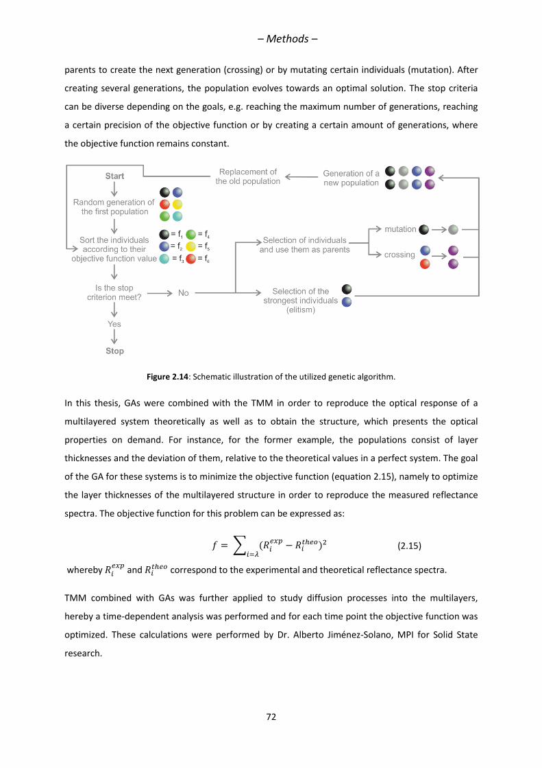
– Methods –
72
parents to create the next generation (crossing) or by mutating certain individuals (mutation). After
creating several generations, the population evolves towards an optimal solution. The stop criteria
can be diverse depending on the goals, e.g. reaching the maximum number of generations, reaching
a certain precision of the objective function or by creating a certain amount of generations, where
the objective function remains constant.
Figure 2.14: Schematic illustration of the utilized genetic algorithm.
In this thesis, GAs were combined with the TMM in order to reproduce the optical response of a
multilayered system theoretically as well as to obtain the structure, which presents the optical
properties on demand. For instance, for the former example, the populations consist of layer
thicknesses and the deviation of them, relative to the theoretical values in a perfect system. The goal
of the GA for these systems is to minimize the objective function (equation 2.15), namely to optimize
the layer thicknesses of the multilayered structure in order to reproduce the measured reflectance
spectra. The objective function for this problem can be expressed as:
(2.15)
whereby
and correspond to the experimental and theoretical reflectance spectra.
TMM combined with GAs was further applied to study diffusion processes into the multilayers,
hereby a time-dependent analysis was performed and for each time point the objective function was
optimized. These calculations were performed by Dr. Alberto Jiménez-Solano, MPI for Solid State
research.
– Methods –
73
2.4 REFERENCES
[1] A. G. Emslie, F. T. Bonner, L. G. Peck, J. Appl. Phys. 1958, 29, 858-862.
[2] M. D. Tyona, Adv. Mater. Res. 2013, 2, 195-208.
[3] N. C. Thomas, J. Chem. Educ. 1991, 68, 631.
[4] I. Newton, Phil. Trans. Roy. Soc. 1672, 5, 3075.
[5] J. v. Fraunhofer, J. Ann. Phys. 1817, 26, 264.
[6] G. Kirchhoff, Ann. Phys. 1860, 185, 275-301.
[7] G. Kirchhoff, Ann. Phys. 1860, 185, 148-150.
[8] N. Bohr, The theory of spectra and atomic constitution, The University Press, Cambridge Eng.,
1922.
[9] N. Bohr, On the quantum theory of line-spectra, A. F. Høst, København, 1918.
[10] I. R. Altemose, J. Chem. Educ. 1986, 63, A216.
[11] L. R. Koller, Ultraviolet radiation, 2d ed., Wiley, New York, 1965.
[12] A. Cary, History of High Performance UV-Vis-NIR Spectroscopy, Varian.
[13] H. H. Perkampus, UV-VIS spectroscopy and its applications, Springer-Verlag, 1992.
[14] M. Bass, O. S. o. America, Handbook of optics, McGraw-Hill, 2001.
[15] Bronkhorst-High-Tech, https://www.bronkhorst.com/products/liquid-flow/, accessed on
13.03.2018.
[16] H. J. Boer, Liquid-Injection System Based on Mass Flow Controllers, Solid State Technol. 1996.
[17] Fundamentals of Mass Flow Control: Critical Terminology and Operation Principles for Gas and
Liquid MFCs; Advance Energy Ltd., Fort Collins, Colorado, 2005.
[18] Bronkhorst-High-Tech, Vol. 2015, www.fluidat.com, accessed on 13.03.2018.
[19] P. Drude, Ann. Phys. 1887, 268, 584-625.
[20] P. Drude, Ann. Phys. 1891, 279, 126-157.
[21] D. E. Aspnes, A. A. Studna, Appl. Opt. 1975, 14, 220-228.
[22] R. H. Muller, J. C. Farmer, Rev. Sci. Instrum. 1984, 55, 371-374.
[23] H. Fujiwara, Spectroscopic Ellipsometry, John Wiley & Sons, Ltd, 2007, pp. 1-11.
[24] H. Fujiwara, Spectroscopic Ellipsometry, John Wiley & Sons, Ltd, 2007, pp. 81-146.
[25] S. P. Pavunny, R. Thomas, R. S. Katiyar, ECS Trans. 2012, 45, 219-223.
[26] Y. T. Kim, R. W. Collins, K. Vedam, Surf. Sci. 1990, 233, 341-350.
[27] M. R. Baklanov, K. P. Mogilnikov, V. G. Polovinkin, F. N. Dultsev, J. Vac. Sci. Technol., B:
Microelectron. Nanometer Struct.-Process., Meas., Phenom. 2000, 18, 1385-1391.
[28] https://goldbook.iupac.org, accessed on 06.02.2018.
[29] S. Deniard-Courant, Y. Piffard, P. Barboux, J. Livage, Solid State Ionics 1988, 27, 189-194.
– Methods –
74
[30] K. Szendrei, P. Ganter, O. Sánchez-Sobrado, R. Eger, A. Kuhn, B. V. Lotsch, Adv. Mater. 2015,
27, 6341-6348.
[31] E.-P. Ng, S. Mintova, Microporous Mesoporous Mater. 2008, 114, 1-26.
[32] B. Valeur, M. N. Berberan-Santos, J. Chem. Edu. 2011, 88, 731-738.
[33] G. G. Stokes, Philos. Trans. R. Soc. London 1852, 142, 463-562.
[34] G. G. Stokes, Philos. Trans. R. Soc. London 1853, 143, 385-396.
[35] E. Becquerel, La lumière, ses causes et ses effets: Effets de la lumière, Firmin Didot frères, fils et
cie, 1868.
[36] A. Einstein, Ann. Phys. 2005, 14, 280-291.
[37] C. R. Ronda, Luminescence: From Theory to Applications, Wiley, 2008.
[38] https://www.nobelprize.org/educational/physics/microscopes/fluorescence/, accessed on
02.02.2018.
[39] K. Przibram, Irradiation Colours and Luminescence: A Contribution to Mineral Physics,
Pergamon Press, 1956.
[40] A. Jiménez-Solano, PhD thesis, ICMSE-CSIS, Sevilla, Spain, 2017.
[41] A. Jiménez-Solano, J. F. Galisteo-López, H. Míguez, Small 2015, 11, 2727-2732.
[42] M. Knoll, Zeitschrift für technische Physik 1935, 16, 467-475.
[43] M. von Ardenne, Improvements in electron microscopes, 1939, GB19380005181 19380218.
[44] M. von Ardenne, Z. Phys. 1938, 109, 553-572.
[45] V. A. Zworykin, Hillier, J., Snyder R. L., ASTM Bull. 1942, 117, 15-23.
[46] C. W. Oatley, The Early History of the Scanning Electron Microscope, University of Cambridge
Department of Engineering, 1979.
[47] C. W. Oatley, T. E. Evekhart, J. Electron. Control 1957, 2, 568-570.
[48] E. Abbe, Archiv für mikroskopische Anatomie 1873, 9, 413-418.
[49] D. B. Williams, C. B. Carter, Transmission Electron Microscopy: A Textbook for Materials
Science, Springer, 2009.
[50] https://www.nobelprize.org/educational/physics/microscopes/tem/, accessed on 1.3.2018.
[51] L. Reimer, H. Kohl, Transmission Electron Microscopy: Physics of Image Formation, Springer
New York, 2008.
[52] P. K. Dash, P. B. S. Murty, R. B. K. Aamanchi, Am. J. Nanomater. 2015, 3, 28-39.
[53] K. Szendrei-Temesi, O. Sanchez-Sobrado, S. B. Betzler, K. M. Durner, T. Holzmann, B. V. Lotsch,
Adv. Func. Mater., 2018, 28, 1705740.
[54] R. F. Egerton, Electron Energy-Loss Spectroscopy in the Electron Microscope, Springer US, New
York, US, 2011.
– Methods –
75
[55] F. Hofer, F. P. Schmidt, W. Grogger, G. Kothleitner, IOP Conf. Ser.: Mater. Sci. Eng. 2016, 109,
012007.
[56] https://www.nobelprize.org/nobel_prizes/physics/laureates/1901/, accessed on 18.02.2018.
[57] https://www.nobelprize.org/nobel_prizes/physics/laureates/1914/, accessed on 18.02.2018.
[58] https://www.nobelprize.org/nobel_prizes/physics/laureates/1915/, accessed on 18.02.2018.
[59] R. A. Gordon, D. Yang, E. D. Crozier, D. T. Jiang, R. F. Frindt, Phys. Rev. B: Condens. Matter
Mater. Phys. 2002, 65, 125407/125401-125407/125409.
[60] D. Yang, R. F. Frindt, J. Mater. Res. 1996, 11, 1733-1738.
[61] W. SEARCH, Vers. 2.08, 2005.
[62] WINXPOW, Vers. 2.12, 2005.
[63] S. Kabekkodu, International Centre for Diffraction Data, Newtown Square, PA, USA 2010.
[64] D. K. Carpenter, J. Chem. Educ. 1977, 54, A430.
[65] L. Rayleigh, The London, Edinburgh, and Dublin Philosophical Magazine and Journal of Science
1881, 12, 81-101.
[66] G. Mie, Ann.Phys. 1908, 330, 377-445.
[67] A. Einstein, Ann. Phys. 2005, 14, 368-391.
[68] R. Pecora, J. Chem. Phys. 1964, 40, 1604-1614.
[69] G. Haugstad, Atomic Force Microscopy: Understanding Basic Modes and Advanced
Applications, Wiley, 2012.
[70] https://www.nobelprize.org/nobel_prizes/physics/laureates/1986/, accessed on19.02.2018.
[71] G. Binnig, C. F. Quate, C. Gerber, Phys. Rev. Lett. 1986, 56, 930-933.
[72] G. K. Bennig, Atomic force microscope and method for imaging surfaces with atomic resolution,
US4724318A, 1988.
[73] P. Eaton, P. West, Atomic Force Microscopy, OUP Oxford, 2010.
[74] F. J. Giessibl, Reviews of Modern Physics 2003, 75, 949-983.
[75] E. Hecht, Optics, Addison-Wesley, Reading, Mass., 2002.
[76] P. Yeh, Optical waves in layered media, Wiley-Interscience, Hoboken, 2005.
[77] J. H. Holland, Adaptation in Natural and Artificial Systems: An Introductory Analysis with
Applications to Biology, Control and Artificial Intelligence, MIT Press, 1992.
[78] D. E. Goldberg, Genetic Algorithms in Search, Optimization and Machine Learning,
Addison-Wesley Longman Publishing Co., Inc., 1989.

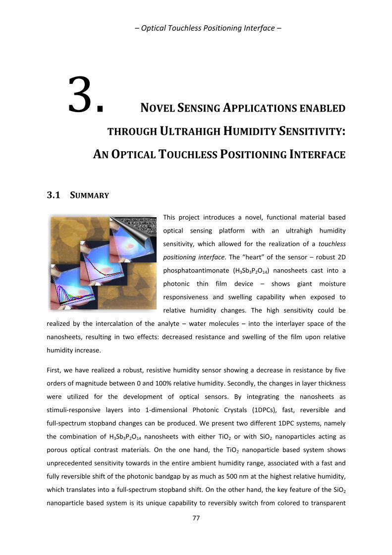
– Optical Touchless Positioning Interface –
77
3. NOVEL SENSING APPLICATIONS ENABLED
THROUGH ULTRAHIGH HUMIDITY SENSITIVITY:
AN OPTICAL TOUCHLESS POSITIONING INTERFACE
3.1 SUMMARY
This project introduces a novel, functional material based
optical sensing platform with an ultrahigh humidity
sensitivity, which allowed for the realization of a touchless
positioning interface. The “heart” of the sensor – robust 2D
phosphatoantimonate (H3Sb3P2O14) nanosheets cast into a
photonic thin film device – shows giant moisture
responsiveness and swelling capability when exposed to
relative humidity changes. The high sensitivity could be
realized by the intercalation of the analyte – water molecules – into the interlayer space of the
nanosheets, resulting in two effects: decreased resistance and swelling of the film upon relative
humidity increase.
First, we have realized a robust, resistive humidity sensor showing a decrease in resistance by five
orders of magnitude between 0 and 100% relative humidity. Secondly, the changes in layer thickness
were utilized for the development of optical sensors. By integrating the nanosheets as
stimuli-responsive layers into 1-dimensional Photonic Crystals (1DPCs), fast, reversible and
full-spectrum stopband changes can be produced. We present two different 1DPC systems, namely
the combination of H3Sb3P2O14 nanosheets with either TiO2 or with SiO2 nanoparticles acting as
porous optical contrast materials. On the one hand, the TiO2 nanoparticle based system shows
unprecedented sensitivity towards in the entire ambient humidity range, associated with a fast and
fully reversible shift of the photonic bandgap by as much as 500 nm at the highest relative humidity,
which translates into a full-spectrum stopband shift. On the other hand, the key feature of the SiO2
nanoparticle based system is its unique capability to reversibly switch from colored to transparent

– Optical Touchless Positioning Interface –
78
(and vice versa) due to humidity-induced refractive index matching of the constituent layers,
rendering it a promising candidate for applications in ambient monitoring, such as smart windows.
The combination of beneficial sensing properties, such as fast response times in the subsecond
range, high reversibility, and large signal changes allow these devices to detect the humidity sheath
of a human finger and also track finger motions across the sensor surface in real-time and real-color
in a touchless fashion. To the best of our knowledge, this is the first example of a photonic approach
to next-generation touchless positioning interfaces and tracking devices.Besides, for the resistive
device, we could create an axial touchless positioning interface with a 170-fold resistive signal change
between finger-on and finger-off states, which is significant and appropriate for these applications.
Contributions: Katalin Szendrei optimized the nanosheet based thin film fabrication, designed and
fabricated the 1DPCs, performed the theoretical calculations in order to understand the sensing
mechanism, characterized the 1DPCs in optical sensing applications and in touchless devices, wrote
the manuscript and edited the figures. Pirmin Ganter synthesized, exfoliated and characterized the
H3Sb3P2O14 nanosheets, fabricated the resistive thin film devices, performed the resistivity
measurements, characterized the fabricated systems as resistive humidity sensors and resistive
touchless positioning interfaces, wrote the manuscript and edited the figures. Olalla
Sánchez-Sobrado assisted with the optical measurements and with the theoretical calculations and
helped with writing the manuscript. Roland Eger synthesized and characterized the bulk K3Sb3P2O14
and the protonated H3Sb3P2O14. Alexander Kuhn proposed the idea of using the H3Sb3P2O14
nanosheets in humidity sensing applications and in touchless devices and helped writing the
manuscript.
This project and the work described in Chapter 5 and an oral presentation at the Spring Meeting of
the Material Research Society (MRS) in Phoenix, USA, in 2017 was awarded with the Graduate
Student Silver award.
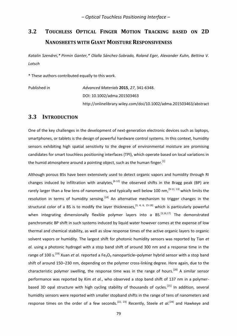
– Optical Touchless Positioning Interface –
79
3.2 TOUCHLESS OPTICAL FINGER MOTION TRACKING BASED ON 2D
NANOSHEETS WITH GIANT MOISTURE RESPONSIVENESS
Katalin Szendrei,* Pirmin Ganter,* Olalla Sánchez-Sobrado, Roland Eger, Alexander Kuhn, Bettina V.
Lotsch
* These authors contributed equally to this work.
Published in Advanced Materials 2015, 27, 341-6348.
DOI: 10.1002/adma.201503463
http://onlinelibrary.wiley.com/doi/10.1002/adma.201503463/abstract
3.3 INTRODUCTION
One of the key challenges in the development of next-generation electronic devices such as laptops,
smartphones, or tablets is the design of powerful hardware control systems. In this context, humidity
sensors exhibiting high spatial sensitivity to the degree of environmental moisture are promising
candidates for smart touchless positioning interfaces (TPI), which operate based on local variations in
the humid atmosphere around a pointing object, such as the human finger.[1]
Although porous BSs have been extensively used to detect organic vapors and humidity through RI
changes induced by infiltration with analytes,[6-12] the observed shifts in the Bragg peak (BP) are
rarely larger than a few tens of nanometers, and typically well below 100 nm,[9-11, 13] which limits the
resolution in terms of humidity sensing.[14] An alternative mechanism to trigger changes in the
structural color of a BS is to modify the layer thicknesses,[3, 4, 6, 15-18] which is particularly powerful
when integrating dimensionally flexible polymer layers into a BS.[3,16,17] The demonstrated
panchromatic BP shift in such systems induced by liquid water however comes at the expense of low
thermal and chemical stability, as well as slow response times of the active organic layers to organic
solvent vapors or humidity. The largest shift for photonic humidity sensors was reported by Tian et
al. using a photonic hydrogel with a stop band shift of around 300 nm and a response time in the
range of 100 s.[19] Xuan et al. reported a Fe2O3 nanoparticle–polymer hybrid sensor with a stop band
shift of around 150–230 nm, depending on the polymer cross-linking degree. Here again, due to the
characteristic polymer swelling, the response time was in the range of hours.[20] A similar sensor
performance was reported by Kim et al., who observed a stop band shift of 137 nm in a polymer-
based 3D opal structure with high cycling stability of thousands of cycles.[21] In addition, several
humidity sensors were reported with smaller stopband shifts in the range of tens of nanometers and
response times on the order of a few seconds.[22, 23] Recently, Steele et al.[24] and Hawkeye and
– Optical Touchless Positioning Interface –
80
Brett[25] presented mesoporous TiO2 gratings used for humidity applications, which show an ultrafast
response time in the subsecond range, but rather small stop band shifts (and therefore resolution)
on the order of 30 nm.
Here, we replace the dimensionally flexible organic component in BS by phosphatoantimonic acid
H3Sb3P2O14 nanosheets[26, 27] with giant moisture responsiveness. The protonic bulk material, which
has long been known for its remarkable swelling characteristics driven by moisture and the resulting
humidity-dependent proton conductivity,[28, 29] can be readily delaminated into 2D nanosheets, giving
rise to stable liquid crystalline suspensions with anisotropic optical properties.[26, 27]
The integration of other 2D nanosheets into resistive sensing devices has already led to a superior
sensing performance as compared to the corresponding bulk materials, exemplified by a VS2
nanosheet-based TPI featuring moisture-sensitive electric, rather than ionic conductance.[1] While
flexible in their design, these resistive VS2 nanosheet sensors have certain drawbacks such as low
chemical stability under ambient conditions and rather poor sensitivity. Further examples of
nanosheet-based humidity sensors include NbS2,[30] graphene oxide,[31, 32] MoS2,
[33] and ZnO.[34] Nearly
all of these nanosheet sensors have either slow response times (e.g., 600 s for ZnO),[34] or low
sensitivity[30,32,33] (e.g., factor 5 increase in resistance for a change from 6% RH to 74% RH for NbS2).[30]
Therefore, it still remains a major challenge to design nanosheet-based humidity sensors for
real-time interaction devices with sufficient sensitivity.
In this work, we fashion thin films of phosphatoantimonic acid nanosheets into chemically stable,
transparent, and low-cost humidity sensing devices operating either with resistive or optical read
out, both of which can be applied as TPI based on spatially resolved humidity tracking. Drawing on
the smoother (i.e., less stepwise) relative humidity (RH)-dependent swelling behavior of the
nanosheets compared to the bulk material[28] and the fabrication of mechanically stable, yet flexible
thin films, we detect a significantly enhanced response to a humid pointer as compared to existing
devices. The novel optical TPI introduced in this work is capable of contactless finger movement
tracking through a combination of unique features such as ultra large stop band shift (>500 nm),
along with reversible transparency switching and a fast response time.
3.4 RESULTS AND DISCUSSION
The layered phosphatoantimonate K3Sb3P2O14 and the proton exchanged phosphatoantimonic acid
H3Sb3P2O14 (Figure S 3.1, Supporting Information) were synthesized by a conventional solid-state
reaction followed by ion-exchange with 8 M HNO3 (Figures S 3.2, S 3.3, Table S 3.1, Supporting
Information).[28, 35] The protonation and exfoliation process in pure water is schematically shown in
– Optical Touchless Positioning Interface –
81
Figure 3.1a. The schlieren texture and the Tyndall effect of the resulting aqueous suspension indicate
successful delamination and the anisotropic nature of the nanosheets (Figure S 3.4, Supporting
Information), while drop-casting the suspension gives rise to randomly overlapping, c-oriented
nanosheets (Figure 3.1b,c; Figures S 3.5, S 3.6, Supporting Information). The thickness of the
Sb3P2O143− nanosheets as determined by AFM amounts to 1.3 ± 0.1 nm on average (Figure 3.1b),
which agrees well with the crystallographic thickness of 1.10 nm for a single Sb3P2O143− layer.[26, 35]
Transmission electron microscopy–energy dispersive X-ray (TEM–EDX) analysis and scanning electron
microscopy-energy dispersive X-ray (SEM–EDX) analysis confirm the expected elemental composition
(Tables S 3.2 and S 3.3, Supporting Information) and the d values of the selected area diffraction
(SAD) pattern agree well with those of the nanosheet pellet by powder X-ray diffraction (XRD) (Table
S 3.4, Supporting Information). The XRD pattern of a turbostratically disorderd nanosheet pellet
obtained by centrifugation at 18000 rpm can be indexed on the basis of a trigonal layer group (Figure
S 3.7, Supporting Information) and exhibits Warren like peak profiles of the (hk) reflections typical of
2D materials.[36, 37]
Nanosheet thin films with thicknesses around 100 nm can directly be used as resistive humidity
sensors. The transparent thin film device is displayed in Figure S 3.8 (Supporting Information) along
with two SEM cross-section images from different areas, which illustrate the ultrathin nature of the
device. Drawing on the well-known moisture-dependent proton conductivity of phosphatoantimonic
acid,[28] we first measured the RH-dependent ionic conductance between 0% and 100% RH using two
methods, a gas flow setup and saturated salt solutions (for details see Figure 3.1d; Figures S 3.8, S
3.9, S 3.10, Supporting Information). Remarkably, we observed an increase in conductance of the
sample with increasing RH by five orders of magnitude over the complete humidity range, with only a
small hysteresis loop (Figure 3.1d), which is at least three orders of magnitude larger than that
observed for VS2 nanosheet devices. To the best of our knowledge, this level of sensitivity is the
highest observed for any nanosheet-based conductance or resistance humidity sensor reported to
date.[1,30-34] The cycling behavior of the thin film device between 0% and 47% RH shows good
reversibility (Figure 3.1e).[38] Notably, the RH dependence of the proton conductance of our thin film
device is quite different from that of phosphatoantimonic acid bulk material reported in the
literature.[28] While the bulk material shows distinct step like behavior, this is not the case for the
nanosheet film device. We attribute the smoother increase in conductance to the smaller particle
size, leading to an increased amount of grain boundary adsorption, and to the non uniform interlayer
space resulting in less well-defined water adsorption sites between the randomly oriented
nanosheets. Such textural effects likely change the water uptake mechanism from that of a lattice
hydrate (bulk material) to that of a particle hydrate (nanosheets), which accommodates a large
amount of water molecules on the internal and external surfaces of the nanosheets.

– Optical Touchless Positioning Interface –
82
To further explore the sensing capabilities of the phosphatoantimonate nanosheets, thin films with
tunable thicknesses in the range of 50–150 nm were prepared by spin-coating the colloidal
suspension of exfoliated nanosheets at different spinning speeds. Upon increasing the RH from
0-100%, the nanosheet film swells to the double of its thickness (e.g., Figure S 3.11, Supporting
Information: from 72 to 128 nm). Hereby, a particularly pronounced change is observed in the high
humidity range above 90% RH (112–128 nm) as determined by spectroscopic ellipsometry. This effect
is accompanied by a RI decrease (from 1.62 to 1.52), again with a pronounced drop in the RH range
above 90%, corresponding to the water uptake and the resulting thickness change. The continuous RI
decrease in the higher RH range then is the result of mixing the refractive indices of water (1.33) and
the nanosheets. The RI increase and the nearly unchanged layer thickness in the low humidity range
up to 10% RH are rationalized by the structural pore filling of the randomly restacked nanosheets
(Figure S 3.1, Supporting Information). While the bulk material shows distinct step like swelling
behavior,[28] this is not the case for the nanosheet film device. We attribute the smoother increase to
the same morphology reasons as discussed for the conductance changes.
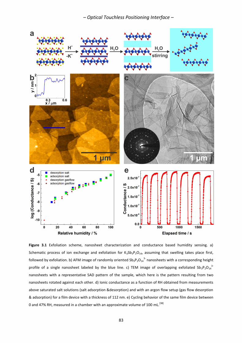
– Optical Touchless Positioning Interface –
83
Figure 3.1 Exfoliation scheme, nanosheet characterization and conductance based humidity sensing. a)
Schematic process of ion exchange and exfoliation for K3Sb3P2O14, assuming that swelling takes place first,
followed by exfoliation. b) AFM image of randomly oriented Sb3P2O143-
nanosheets with a corresponding height
profile of a single nanosheet labeled by the blue line. c) TEM image of overlapping exfoliated Sb3P2O143-
nanosheets with a representative SAD pattern of the sample, which here is the pattern resulting from two
nanosheets rotated against each other. d) Ionic conductance as a function of RH obtained from measurements
above saturated salt solutions (salt adsorption &desorption) and with an argon flow setup (gas flow desorption
& adsorption) for a film device with a thickness of 112 nm. e) Cycling behavior of the same film device between
0 and 47% RH, measured in a chamber with an approximate volume of 100 mL.[38]
– Optical Touchless Positioning Interface –
84
Inspired by the unprecedentedly large swelling properties of the nanosheet films, BSs were
assembled from H3Sb3P2O14 nanosheets as the humidity-sensitive component and either TiO2 or SiO2
nanoparticle layers providing the required RI contrast. At ambient air (30% RH), the nanosheet film
shows a refractive index of 1.56 as determined by spectroscopic ellipsometry (Figure S 3.11b,
Supporting Information). While TiO2 nanoparticles exhibit a higher RI (1.85), SiO2 nanoparticle layers
show a lower RI (1.35) Figure S 3.12 (Supporting Information). The particle nature of the TiO2 and
SiO2 layers acts as a gate, ensuring the access of the water molecules to the moisture-sensitive
nanosheet layers through textural porosity.[10] Figure 3.2a,b show cross sectional SEM images of two
BSs containing 12 and 11 alternating layers of H3Sb3P2O14 nanosheets and SiO2 and TiO2
nanoparticles, respectively, evidencing long range stacking order and lateral layer uniformity across
at least several microns. The spectral position of the first-order BP maximum and, hence, the
structural color at normal incidence is given by Equation (1):[39]
= 2 (n1d1 + n2d2) (1)
where n1 and n2 are the RIs of the different layers and d1 and d2 their respective thicknesses.
The BSs depicted in Figure 3.2c (H3Sb3P2O14/SiO2) and 2d (H3Sb3P2O14/TiO2) show pronounced
structural colors, which can be judiciously adjusted and gradually fine-tuned during the fabrication
procedure across the visible spectrum.
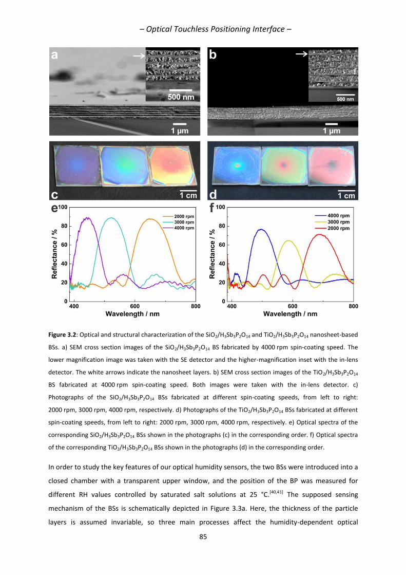
– Optical Touchless Positioning Interface –
85
Figure 3.2: Optical and structural characterization of the SiO2/H3Sb3P2O14 and TiO2/H3Sb3P2O14 nanosheet-based
BSs. a) SEM cross section images of the SiO2/H3Sb3P2O14 BS fabricated by 4000 rpm spin-coating speed. The
lower magnification image was taken with the SE detector and the higher-magnification inset with the in-lens
detector. The white arrows indicate the nanosheet layers. b) SEM cross section images of the TiO2/H3Sb3P2O14
BS fabricated at 4000 rpm spin-coating speed. Both images were taken with the in-lens detector. c)
Photographs of the SiO2/H3Sb3P2O14 BSs fabricated at different spin-coating speeds, from left to right:
2000 rpm, 3000 rpm, 4000 rpm, respectively. d) Photographs of the TiO2/H3Sb3P2O14 BSs fabricated at different
spin-coating speeds, from left to right: 2000 rpm, 3000 rpm, 4000 rpm, respectively. e) Optical spectra of the
corresponding SiO2/H3Sb3P2O14 BSs shown in the photographs (c) in the corresponding order. f) Optical spectra
of the corresponding TiO2/H3Sb3P2O14 BSs shown in the photographs (d) in the corresponding order.
In order to study the key features of our optical humidity sensors, the two BSs were introduced into a
closed chamber with a transparent upper window, and the position of the BP was measured for
different RH values controlled by saturated salt solutions at 25 °C.[40,41] The supposed sensing
mechanism of the BSs is schematically depicted in Figure 3.3a. Here, the thickness of the particle
layers is assumed invariable, so three main processes affect the humidity-dependent optical
– Optical Touchless Positioning Interface –
86
response of the BS: i) The RI changes of the TiO2 and SiO2 nanoparticle layers with the
adsorption/desorption of water into their textural pores (i.e., interparticle voids, Figure S 3.12,
Supporting Information), ii) the change of the RI of the nanosheet layers through uptake/loss of
water (Figure S 3.11b, Supporting Information), iii) the humidity-dependent thickness of the
nanosheet layers (Figure S 3.11a, Supporting Information). While for SiO2 and TiO2 the effective RI of
the layers increases with increasing water content due to the pore filling process, it decreases for the
nanosheet layers as the effective RI approaches that of pure water with increasing degree of
hydration. The latter phenomenon is driven by the massive swelling of the nanosheet layers in
contrast to the more compact nanoparticle layers. These features can be extracted from the
humidity-dependent reflectance spectrum and the overall optical changes can also be monitored as
color changes with the naked eye. The two BSs qualitatively behave differently: In the
H3Sb3P2O14/SiO2 BS, the photonic stop band red-shifts by 100 nm in the lower RH range (up to 90%)
as plotted in Figure 3.3b (solid lines). The set of microscope images shown below corresponds to the
color displayed by the BS for three different RH values (32%, 93%, 100%). For increasing values of the
RH, the BP redshifts, while its reflectance intensity gradually decreases and finally vanishes
(Figure 3.3b, black spectrum). The color displayed by the sensor (Figure 3.3c) follows this behavior
and for the highest value of humidity, the 1DPC switches off, i.e., becomes completely transparent
(Figure S 3.13, Supporting Information). This effect finds its explanation in the elimination of the
optical contrast between the layers forming the BS with increasing RH. While the RI of the particle
layer increases and its thickness roughly remains constant, the RI of the nanosheet layer decreases
while the layer thickness increases, leading to an overall redshift of the BP. Since the RIs of the
nanosheet and nanoparticle layers follow opposite trends, both values ultimately become nearly
equal at above 95% RH, leading to the disappearance of the optical contrast. As the BP is canceled
out, the optical sensor turns completely transparent and light is transmitted by the structure
throughout the visible range (Figure S 3.13, Supporting Information). Complete transparency
switching through reversible refractive index matching has previously been realized by rational
porosity and refractive index tuning of the constituent layers.[42, 43] These hygrochromic multilayers
however are only capable of detecting liquid water, rather than humidity sensors.
The specular reflectance spectra taken for the TiO2/H3Sb3P2O14 BS are plotted in Figure 3.3d (solid
lines), along with the corresponding surfaces of the BS for different RH values (Figure 3.3e). The BP
redshifts by 100 nm in the RH range of 0–90%. Contrary to the SiO2 containing BS, the reflectance
rises with increasing RH and the stop band broadens, which can be rationalized by the increase in
optical contrast of the layers with increasing RH. We observe a total redshift of more than 517 nm,
shifting the BP out of the visible range into the IR, while the second-order BP is observed at 495 nm
(red curve of Figure 3.3d). The observed red shift at high RH is the largest ever observed for a BS for
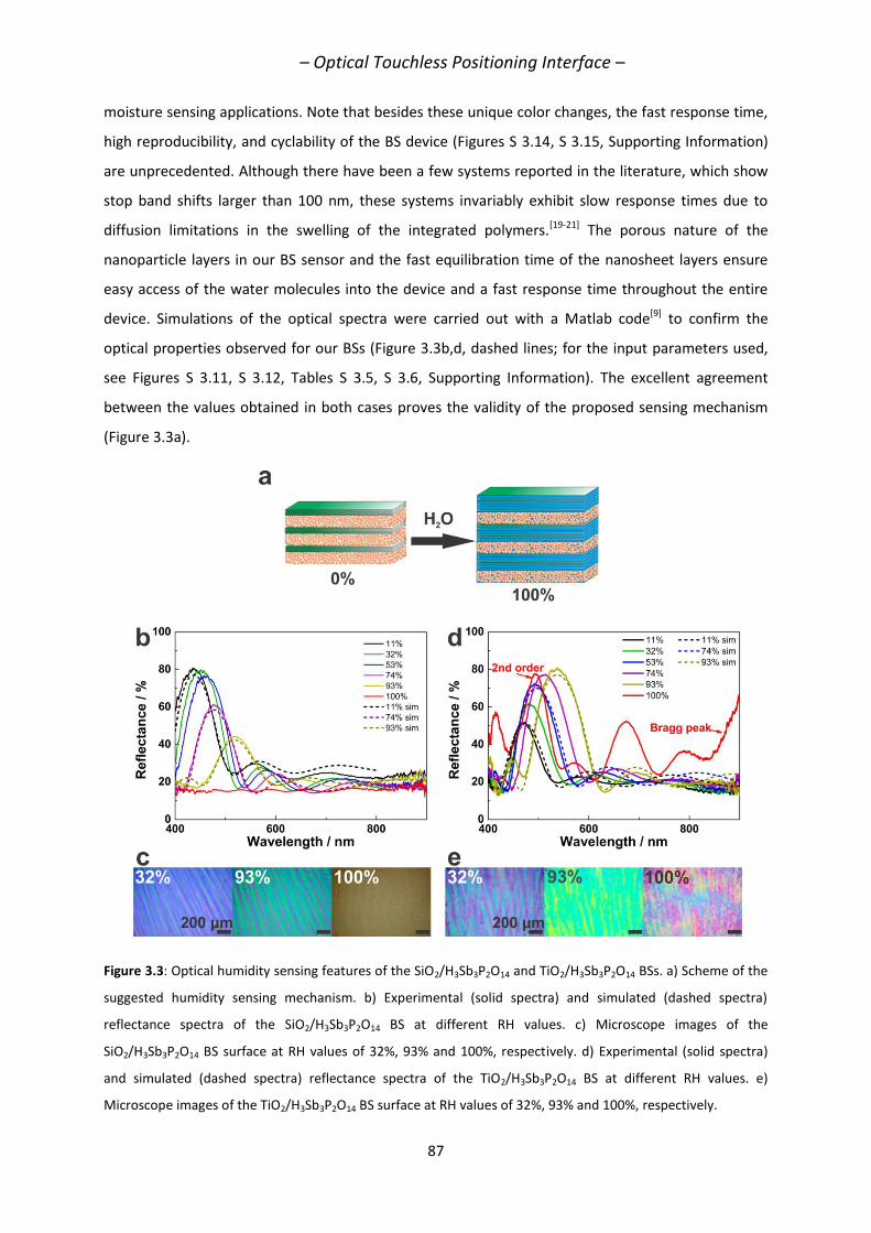
– Optical Touchless Positioning Interface –
87
moisture sensing applications. Note that besides these unique color changes, the fast response time,
high reproducibility, and cyclability of the BS device (Figures S 3.14, S 3.15, Supporting Information)
are unprecedented. Although there have been a few systems reported in the literature, which show
stop band shifts larger than 100 nm, these systems invariably exhibit slow response times due to
diffusion limitations in the swelling of the integrated polymers.[19-21] The porous nature of the
nanoparticle layers in our BS sensor and the fast equilibration time of the nanosheet layers ensure
easy access of the water molecules into the device and a fast response time throughout the entire
device. Simulations of the optical spectra were carried out with a Matlab code[9] to confirm the
optical properties observed for our BSs (Figure 3.3b,d, dashed lines; for the input parameters used,
see Figures S 3.11, S 3.12, Tables S 3.5, S 3.6, Supporting Information). The excellent agreement
between the values obtained in both cases proves the validity of the proposed sensing mechanism
(Figure 3.3a).
Figure 3.3: Optical humidity sensing features of the SiO2/H3Sb3P2O14 and TiO2/H3Sb3P2O14 BSs. a) Scheme of the
suggested humidity sensing mechanism. b) Experimental (solid spectra) and simulated (dashed spectra)
reflectance spectra of the SiO2/H3Sb3P2O14 BS at different RH values. c) Microscope images of the
SiO2/H3Sb3P2O14 BS surface at RH values of 32%, 93% and 100%, respectively. d) Experimental (solid spectra)
and simulated (dashed spectra) reflectance spectra of the TiO2/H3Sb3P2O14 BS at different RH values. e)
Microscope images of the TiO2/H3Sb3P2O14 BS surface at RH values of 32%, 93% and 100%, respectively.
– Optical Touchless Positioning Interface –
88
Both, the conductance of the nanosheet thin film and the optical properties of the BSs show a
reproducible, fast, and selective response to changes in RH, which are important performance
parameters for position-sensitive user control interfaces. Since the fingertip is surrounded by a
distance dependent humidity atmosphere, the read-out schemes developed above present intriguing
candidates for the development of 3D (i.e., lateral and height-sensitive) non-contact interactive
interfaces. To probe the touchless sensing capability of our nanosheet thin films and the Bragg stack,
first, the nanosheet film on a quartz substrate was studied. Hereby, an increase of the conductance
by more than a factor of 170 was observed when the distance of the finger from the sensor surface
was reduced from 1.6 to 0.1 cm at 30% ambient RH (Figure 3.4a). This is notably higher than the
values recently reported for VS2 or graphene oxide thin film devices with a reported 3- or 0.35-fold
signal increase.[1,32] Note also that the fast full response (<2 s) and recovery times (3 s) towards
“tapping” finger motion even allow to resolve subsecond events as shown in Figure S 3.16
(Supporting Information). The observed response times are rather fast compared to other
nanostructured humidity sensing devices with typical response times on the order of tens to
hundreds of seconds,[34,44-47] and even faster than those of state-of-the-art resistive sensors based on
GO or VS2,[1,32] or commercially available sensors.[48-50]
The finger-tip induced conductance changes monitored in a dynamic measurement (Video S1,
Supporting Information) also demonstrate that the thin film device indeed has a very fast and
reversible response to finger distance changes.
With the highly sensitive photonic read-out scheme presented above, the tools are at hand to go one
step further and develop a novel optical TPI based on the lateral tracking of a humid pointer with an
optical read-out visible by the naked eye. For such optical devices, no integration with an electronic
assembly is necessary to visualize the lateral finger position above a photonic surface. Our
experiments, which demonstrate the feasibility of this touchless optical sensing principle, are
summarized in Figure 3.4 and visualized by Videos S2, S3, S4, and S5 (Supporting Information).
Positioning the finger in a vertical distance of 1 mm from both presented BS surfaces leads to a color
gradient along a distance between 1.0 and 1.8 mm from the finger tip, as shown in the microscope
pictures corresponding to the two configurations proposed for TiO2/H3Sb3P2O14 and SiO2/H3Sb3P2O14
BSs, respectively (Figure 3.4d,e). This is in perfect agreement with the conductance behavior, as in
the small distance range the sensing signal drops similarly fast (Figure 3.4a) due to the spatially
dependent humidity gradient around the finger. Looking at the structural colors of the gradient, the
color at 1.0 mm real distance corresponds to the 100% RH sensing signal (where the optical contrast
and reflectance are lost) in the case of the SiO2/H3Sb3P2O14 BS. In both cases, the structural color for a
distance of 1.5 mm corresponds to a RH of around 90% (see Figure 3.3). In Figure S 3.17 (Supporting
– Optical Touchless Positioning Interface –
89
Information), we show that the Bragg stack can be operated as a TPI also at longer distances up to
≈12 mm. The stop band shift is observed immediately (Figure 3.4f,g), and the captured reflectance
spectra for the SiO2/H3Sb3P2O14 BS show a response time of 3 s (defined as the time it takes for 90%
of the stopband shift before the structural color vanishes). Further cycling experiments (Figures
S 3.18, S 3.19, and S 3.20, Supporting Information) demonstrate that a SiO2/H3Sb3P2O14 BS responds
instantaneously to fast “tapping” finger motion, resulting in a subsecond time resolution (note that
the “tapping” motion was also carried out under touchless conditions). The fast response is also
obvious from lateral movement of the finger across the BS (Figure 3.4h–l, Video S5, Supporting
Information). An instantaneous color response precisely following the finger movement was
observed, which is equivalent to a high-accuracy tracking of the finger movement (see Figure 3.4h–l,
Video S5, Supporting Information). The BS response occurs exclusively due to the local water vapor
atmosphere surrounding the finger, rather than a temperature effect, as: i) the response in the
finger-on state (Video S2, Supporting Information) is completely analogous to the measurement at
very high RH carried out at RT, and ii) no color change is observed if the finger is protected by a nitrile
glove (Figure 3.4c), while a fast and pronounced color change is directly seen by approaching the
naked finger (Figure 3.4b, Figure 3.4h–l). Notably, the humidity response is fully reversible during
cycling (Figure 3.4g inset, Figures S 3.18, S 3.20, Supporting Information) and the Bragg stack can be
cycled for more than 1000 times without observing any signs of degradation (Figures S 3.19, S 3.20,
Supporting Information) or changes in its response behavior. Finally, the Bragg stacks show long term
stability without any loss of functionality after repeated usage and storing them in air for more than
8 months (see Figure S 3.21, Supporting Information).
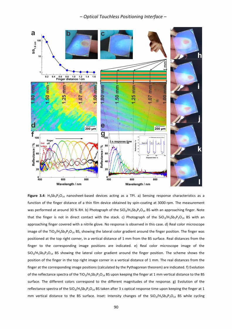
– Optical Touchless Positioning Interface –
90
Figure 3.4: H3Sb3P2O14 nanosheet-based devices acting as a TPI. a) Sensing response characteristics as a
function of the finger distance of a thin film device obtained by spin-coating at 3000 rpm. The measurement
was performed at around 30 % RH. b) Photograph of the SiO2/H3Sb3P2O14 BS with an approaching finger. Note
that the finger is not in direct contact with the stack. c) Photograph of the SiO2/H3Sb3P2O14 BS with an
approaching finger covered with a nitrile glove. No response is observed in this case. d) Real color microscope
image of the TiO2/H3Sb3P2O14 BS, showing the lateral color gradient around the finger position. The finger was
positioned at the top right corner, in a vertical distance of 1 mm from the BS surface. Real distances from the
finger to the corresponding image positions are indicated. e) Real color microscope image of the
SiO2/H3Sb3P2O14 BS showing the lateral color gradient around the finger position. The scheme shows the
position of the finger in the top right image corner in a vertical distance of 1 mm. The real distances from the
finger at the corresponding image positions (calculated by the Pythagorean theorem) are indicated. f) Evolution
of the reflectance spectra of the TiO2/H3Sb3P2O14 BS upon keeping the finger at 1 mm vertical distance to the BS
surface. The different colors correspond to the different magnitudes of the response. g) Evolution of the
reflectance spectra of the SiO2/H3Sb3P2O14 BS taken after 3 s optical response time upon keeping the finger at 1
mm vertical distance to the BS surface. Inset: Intensity changes of the SiO2/H3Sb3P2O14 BS while cycling
– Optical Touchless Positioning Interface –
91
between the finger-on and finger-off states. h-l) Photographs showing the finger movement tracking capability
of the photonic TPI. The pictures are video frames from a similar video as Video S5 taken at 1, 2, 3, 4 and 5
seconds, while the finger was continuously moved laterally along the SiO2/H3Sb3P2O14 Bragg stack without
direct contact with the photonic TPI surface.
In summary, we have demonstrated the potential of phosphatoantimonic acid nanosheet-based
resistive and photonic humidity sensors as TPI, which represents a novel concept complementary to
the contact-based technology. Transparent nanosheet thin films can be applied as a resistive RH
sensor, since the ionic conductance of the film strongly depends on the surrounding RH, featuring
high sensitivity with a response of five orders of magnitude, good cyclability, and ultrafast response
characteristics in the subsecond range. We have demonstrated that due to these properties, the
nanosheet thin film device can be applied as a touchless axial positioning interface with a change of
ionic conductance between the finger on and finger off state by a factor of 170. Further, “smart”
1DPCs were developed as versatile humidity sensors with a simple optical read out. The ultrahigh
stop band shift of 517 nm of the TiO2 based BSs and the switchable transparency through optical
contrast loss of the SiO2 based BSs are unique features of the proposed sensing platform. This second
property, the gradual loss of reflectance accompanied by a color change, makes these multilayers
potential candidates for privacy windows or smart window applications. Due to the straightforward
optical tunability, the extremely high sensitivity, reproducibility, ultrafast response and recovery
times, a new concept of a position-sensitive optical TPI was demonstrated for the first time. As the
humidity-responsive photonic device gives the user direct optical feedback about successful
interaction, no additional soft- and hardware, which is implemented for contact visualization in
current state of the art capacitive touch screens, is needed. Using the contactless optical read out
proposed in this work, the disadvantages of conventional touch screens such as scratches or
fingerprints could be eliminated, while touchless tracking of finger motion is achieved in a simple
fashion without complex electronic circuitry.
3.5 ACKNOWLEDGEMENTS
K. Szendrei and P. Ganter contributed equally to this work. Financial support was granted by the Max
Planck Society, the University of Munich (LMU), the Center for NanoScience (CeNS), and the
Deutsche Forschungsgemeinschaft (DFG) through the Cluster of Excellence „Nanosystems Initiative
Munich” (NIM). B. V. L. gratefully acknowledges financial support by the Fonds der Chemischen
Industrie. The authors thank Viola Duppel for TEM and SEM as well as Claudia Kamella for the
EXD-SEM measurements as well as Willi Hölle for his technical support with the self-built flow setup.
We thank Daniel Selmeczi and the team of Semilab Sopra for their support with the ellipsometry
measurements.
– Optical Touchless Positioning Interface –
92
3.6 REFERENCES
[1] J. Feng, L. Peng, C. Wu, X. Sun, S. Hu, C. Lin, J. Dai, J. Yang, Y. Xie, Adv. Mater. 2012, 24, 1969-
1974.
[2] J. D. Joannopoulos, P. R. Villeneuve, S. Fan, Nature 1997, 386, 143-149.
[3] A. C. Arsenault, T. J. Clark, G. von Freymann, L. Cademartiri, R. Sapienza, J. Bertolotti, E.
Vekris, S. Wong, V. Kitaev, I. Manners, R. Z. Wang, S. John, D. Wiersma, G. A. Ozin, Nat.
Mater. 2006, 5, 179-184.
[4] Z. Wang, J. Zhang, J. Xie, C. Li, Y. Li, S. Liang, Z. Tian, T. Wang, H. Zhang, H. Li, W. Xu, B. Yang,
Adv. Funct. Mater. 2010, 20, 3784-3790.
[5] J. H. Holtz, S. A. Asher, Nature 1997, 389, 829-832.
[6] B. V. Lotsch, G. A. Ozin, Adv. Mater. 2008, 20, 4079-4084.
[7] L. D. Bonifacio, D. P. Puzzo, S. Breslav, B. M. Willey, A. McGeer, G. A. Ozin, Adv. Mater. 2010,
22, 1351-1354.
[8] D. Lee, D. Omolade, R. E. Cohen, M. F. Rubner, Chem. Mater. 2007, 19, 1427-1433.
[9] M. C. Fuertes, S. Colodrero, G. Lozano, A. R. González-Elipe, D. Grosso, C. Boissière, C.
Sánchez, G. J. d. A. A. Soler-Illia, H. Míguez, J. Phys. Chem. C 2008, 112, 3157-3163.
[10] S. Colodrero, M. Ocaña, H. Míguez, Langmuir 2008, 24, 4430-4434.
[11] N. Hidalgo, M. E. Calvo, H. Míguez, Small 2009, 5, 2309-2315.
[12] J. Kobler, B. V. Lotsch, G. A. Ozin, T. Bein, ACS Nano 2009, 3, 1669-1676.
[13] F. M. Hinterholzinger, A. Ranft, J. M. Feckl, B. Ruhle, T. Bein, B. V. Lotsch, J. Mater. Chem.
2012, 22, 10356-10362.
[14] C. Fenzl, T. Hirsch, O. S. Wolfbeis, Angew. Chem. Int. Ed. 2014, 53, 3318-3335.; Angew.
Chem., 2014, 126, 3384-3402.
[15] B. V. Lotsch, G. A. Ozin, ACS Nano 2008, 2, 2065-2074.
[16] Y. Kang, J. J. Walish, T. Gorishnyy, E. L. Thomas, Nat. Mater. 2007, 6, 957-960.
[17] A. C. Arsenault, D. P. Puzzo, I. Manners, G. A. Ozin, Nat. Photonics 2007, 1, 468-472.
[18] F. Castles, S. M. Morris, J. M. C. Hung, M. M. Qasim, A. D. Wright, S. Nosheen, S. S. Choi, B. I.
Outram, S. J. Elston, C. Burgess, L. Hill, T. D. Wilkinson, H. J. Coles, Nat. Mater. 2014, 13, 817-
821.
[19] E. Tian, J. Wang, Y. Zheng, Y. Song, L. Jiang, D. Zhu, J. Mater. Chem. 2008, 18, 1116–1122.
[20] R. Xuan, Q. Wu, Y. Yin, J. Ge, J. Mater. Chem. 2011, 21, 3672–3676.
[21] S. Kim, J. Lee, H. Jeon, H. J. Kim, Appl. Phys. Lett. 2009, 94, 133503.
[22] J. Shi, V. K. S. Hsiao, T. R. Walker, T. J. Huang, Sens. Actuators, B 2008, 129, 391-396.
[23] R. A. Barry, P. Wiltzius, Langmuir 2006, 22, 1369-174.
– Optical Touchless Positioning Interface –
93
[24] J. J. Steele, A. C. van Popta, M. M. Hawkeye, J. C. Sit, M. J. Brett, Sens. Actuators, B 2006, 120,
213-219.
[25] M. M. Hawkeye, M. J. Brett, Adv. Funct. Mater. 2011, 21, 3652-3658.
[26] J.-C. P. Gabriel, F. Camerel, B. J. Lemalre, H. Desvaux, P. Davidson, P. Batall, Nature 2001, 413,
504-508.
[27] F. Camerel, J. C. P. Gabriel, P. Batail, P. Panine, P. Davidson, Langmuir 2003, 19, 10028-10035.
[28] S. Deniard-Courant, Y. Piffard, P. Barboux, J. Livage, Solid State Ionics 1988, 27, 189-194.
[29] Y. Piffard, A. Verbaere, A. Lachgar, S. Deniard-Courant, M. Tournoux, Rev. Chim. Miner. 1986,
23, 766-775.
[30] W. M. R. Divigalpitiya, R. F. Frindt, S. R. Morrison J. Phys. D: Appl. Phys. 1990, 23, 966-970.
[31] S. Borini, R. White, D. Wei, M. Astley, S. Haque, E. Spigone, N. Harris,J. Kivioja, T. Ryhänen,
ACS Nano 2013, 7, 11166-11173.
[32] X. Wang, Z. Xiong, Z. Liu, T. Zhang, Adv. Mater. 2015, 27, 1370-1375.
[33] S.-L. Zhang, H.-H. Choi, H.-Y. Yue, W.-C.Yang, Current Applied Physics 2014, 14, 264-268.
[34] F.-S. Tsai, S.-J. Wang, Sens. Actuators, B 2014, 193, 280-287.
[35] Y. Piffard, A. Lachgar, M. Tournoux, J. Solid State Chem. 1985, 58, 253-256.
[36] D. Yang, R. F. Frindt, J. Appl. Phys. 1996, 79, 2376-2385.
[37] A. Kuhn, T. Holzmann, J. Nuss, B. V. Lotsch, J. Mater. Chem. A 2014, 2, 6100-6106.
[38] For further details on the determination of the response time and measurement of the
response characteristics, see Supporting Information, Figure S 3.16a-c.
[39] J. D. Joannopoulos, S. G. Johnson, J. N. Winn, R. D. Meade, Photonic crystals: molding the
flow of light, Princeton university press, 2011.
[40] P. W. Winston, D. H. Bates, Ecology 1960, 41, 232-237.
[41] L. Greenspan, J. Res. Nat. Bur. Stand. 1977, 81A, 89-96.
[42] M. N. Ghazzal, O. Deparis, J. De Coninck, E. M. Gaigneaux, J. Mater. Chem. C 2013, 1, 6202-
6209.
[43] K. E. Shopsowitz, H. Qi, W. Y. Hamad, M. J. MacLachlan, Nature 2010, 468, 422-425.
[44] H. Jamil, S. S. Batool, Z. Imran, M. Usman, M. A. Rafiq, M. Willander, M. M. Hassan, Ceram.
Int. 2012, 38, 2437-2441.
[45] J. Wang, M.-Y. Su, J.-Q. Qi, L.-Q. Chang, Sens. Actuators, B 2009, 139, 418-424.
[46] Q. Kuang, C. Lao, Z. L. Wang, Z. Xie, L. Zheng, J. Am. Chem. Soc. 2007, 129, 6070-6071.
[47] Y. Zhang, W. Fu, H. Yang, Q. Qi, Y. Zeng, T. Zhang, R. Ge, G. Zou, Appl. Surf. Sci. 2008, 254,
5545-5547.
[48] Sensirion AG, http://www.sensirion.com/en/products/humidity-temperature/, accessed: 05,
2015.

– Optical Touchless Positioning Interface –
94
[49] E+E ELEKTRONIK Gesellschaft m.b.H., http://www.epluse.com/en/products/humidity-
instruments/humidity-sensor/, accessed: 05, 2015.
[50] Vaisala, http://www.vaisala.com/en/products/humidity/Pages/default.aspx, accessed: 05,
2015.
– Practical Aspects of the Optical Touchless Interface –
95
4. PRACTICAL ASPECTS OF THE OPTICAL
TOUCHLESS POSITIONING INTERFACE:
SELECTIVITY, REPRODUCIBILITY, TEMPERATURE
DEPENDENCY
4.1 SUMMARY
In this chapter, important aspects regarding the optical touchless positioning interfaces (Chapter 3)
were studied: the selectivity towards water vapor, the temperature dependency of the optical
response to the presence of a human finger, and the reversibility of the signal change.
In order to test the selectivity towards water vapor, the optical response to another relevant analyte,
i.e. ethanol vapor, was investigated and compared to the optical response of water vapor. As we
know from previous works (Chapter 3), the sensing mechanism of H3Sb3P2O14 nanosheet based thin
films relies on the intercalation of water vapor into the interlayer space, which is highly hydrophilic
due to the charge compensating protons, which are located between the single nanosheet layers. For
the selectivity studies, we chose ethanol as it is also polar and protic – similar to water vapor – and it
is also capable of creating hydrogen bonds with the protons in the nanosheet interlayer space.
However, upon testing the selectivity, a very different optical behavior is observed, namely a slight
stopband shift accompanied by slow response times, which is substantially different from the fast
response times and large stopband shifts caused by water vapor. The differences most likely lay in
the dielectric and other molecule size-related properties, such as the polarity or acidity and cause the
inhibited diffusion of the ethanol molecules throughout the 1DPC.
Further, the temperature dependency of the optical behavior of these humidity sensors was
analyzed. The multilayered structures were tested between 40°C and 0°C, whereby the temperature
increase did not have important impacts on the sensing capability, but the cooling of the sample did.
Upon reaching the dew point, the ambient humidity condenses on the sensor, thus limiting the

– Practical Aspects of the Optical Touchless Interface –
96
sensor’s response below the dew point. Once the temperature rises above the dew point, the
condensed water can be desorbed again and the humidity responsiveness is restored.
Finally, the reversibility and reproducibility of the touchless positioning interface was tested. Hereby,
the humidity response was tested by approaching a human finger, which is surrounded by a
distance-dependent humid atmosphere, responsible for the sensing response. The cycling stability
and reversibility was proven to be stable for at least 100 cycles.
Contributions: Katalin Szendrei fabricated the 1DPCs, performed the spectroscopic and the
ellipsometry measurements and the theoretical calculations, edited the figures and wrote the
manuscript. Pirmin Ganter synthesized and characterized the 2D nanosheets and assisted with the
manuscript writing.
This project was presented at the SPIE Photonics Europe Conference, in Brussels, 2016 and published
as a conference proceeding. It was awarded, together with the work presented in Chapter 3, with the
Best Student Paper award.
– Practical Aspects of the Optical Touchless Interface –
97
4.2 TESTING THE SELECTIVITY, CYCLING STABILTY AND THE
TEMPERATURE DEPENDENCY OF TOUCHLESS FINGER MOTION
TRACKING DEVICES BASED ON 1D PHOTONIC CRYSTALS
Katalin Szendrei, Pirmin Ganter, Bettina V. Lotsch
Published in Proceedings SPIE 9885, Photonic Crystal Materials and Devices XII
doi: 10.1117/12.2227431
https://www.spiedigitallibrary.org/conference-proceedings-of-
SPIE/9885.toc?SSO=1
4.3 ABSTRACT
Thin film devices composed of 2D phosphatoantimonate nanosheets are optically characterized and
by investigating the humidity-induced swelling behavior, the water uptake mechanism was
suggested. By integrating this intrinsically active material into 1D Photonic Crystal devices, the layer
thickness changes caused by humidity changes are translated into an optical signal, a full-spectral
color change, which can be read out by the naked eye. Additionally, a unique property, a reversible
transparency switching at high humidity values is ensured by the optical contrast canceling upon
water adsorption. Besides the large signal changes, the study of the optical response to ethanol
vapor shows a noticeably higher sensitivity to humidity compared to ethanol vapor, justified by the
different intercalation degree into the nanostructure. Based on the ultrahigh sensitivity to humidity,
phosphatoantimonate nanosheet based Bragg stacks were able to detect finger positions and track
finger motions without touching the sensor surface, only by responding to the humidity sheath of the
human finger. The cycling stability and the reversibility of these optical touchless positioning
interfaces are given for more than 100 cycles, as well as the sensing performance at increased
temperatures about 40 °C is unaffected. Although, we found the limits of these devices at the dew
point, as the water-based sensing mechanisms are not applicable below 0 °C anymore, the optical
tracking of the spontaneous and reversible water condensation into the structure can pave the way
towards other sensing applications.
– Practical Aspects of the Optical Touchless Interface –
98
4.4 INTRODUCTION
Bioinspired periodic nanostructures, 1-dimensional Photonic Crystals (PCs) or also referred to as
Bragg stacks (BS) have gained research interest since the 80s, as the theoretical backgrounds were
established and a comprehensive description of the photonic phenomena within these periodic
multilayers was published by Yablonovitch and John.[1,2] Since this basic work, a plethora of different
photonic structures with potential applications was presented in the literature, such as radiation
shielding,[1] wavelength-selective optical filters,[2, 3] and sensing.[4-12] Especially in the field of sensing,
PCs present an important sensor configuration due to the ease of wet chemical bottom-up
fabrication utilizing the spin- or dip-coating technique, low production and time cost, and
well-defined and simply tunable optical properties.[13] PCs exhibit a periodic medium presented by
the alternating refractive index (RI) defines the optical properties by forming a forbidden energy
region for electromagnetic wave in which no waves are allowed propagating the structure. This
“photonic band gap”, the spectral range with the maximum reflection and the minimum
transmission, is defined by the Bragg-Snell law (1):[14, 15]
(1)
whereby m is the order of diffraction, λ the wavelength, n1 and n2 the RIs of the composing materials
and d1 and d2 the layer thicknesses of the structure. According to (1), the photonic band gap or stop
band also determines the “structural color”. Due to the dynamic manipulation of the photonic stop
band by varying the optical thickness (τ = n ) of the constituent layers, these platforms are capable
of translating chemical or physical environmental recognition events, into an optical read-out, a color
change.[16]
Although PC based sensors are competitive candidates to sensors based on other readout
mechanisms, there are some remaining challenges in this research field. According to a review by C.
Fenzl et al.,[17] some crucial points and challenges are currently limiting the performance of PC based
sensors: (1) the selectivity, (2) signal- and sensor stability, (3) larger signal changes gaining a higher
signal resolution and (4) the utilization of simpler readout techniques besides of microscopy and
reflectometry. Previously presented BS based humidity and organic vapor sensors were extensively
discussed in the literature, but due to singly the RI changes upon infiltration, the stop band shifts are
typically small, which massively limits the resolution in terms of vapor sensing.[18,19] An alternative
sensing mechanism to detect environmental changes with a higher resolution was suggested
predominantly for humidity sensors by applying flexible organic polymers.[20-22] These show a
pronounced swelling upon liquid water or water vapor infiltration. In general, the layer thickness
change, e.g. the swelling of the integrated polymers ends up in a massive structural color change of
– Practical Aspects of the Optical Touchless Interface –
99
hundreds of nanometers.[20] Unfortunately, the powerful potential of swelling comes at the expense
of slow response times, low chemical and thermal stability, which restricts these systems for real-life
applications.
Herein, we present humidity responsive Bragg stacks with integrated intrinsically active materials:
robust inorganic 2D phosphatoantimonate nanosheets. The protonated bulk material is known since
the 80s for its remarkable swelling capability driven by humidity changes.[23] This layer distance
changes are attributed due to intercalation of the water molecules between the crystal lattice planes,
whereby the polar character of the containing the protons favors the intercalation. The protonated
bulk material can be readily delaminated into 2D nanosheets, giving rise to stable liquid crystalline
suspensions with anisotropic properties.[24,25] In our previous work, we proved that these phosphato
antimonate nanosheets can be exfoliated in pure water into single nanosheets with a thickness of
1.3±0.1 nm and lateral dimensions of several microns.[26] In this work, we optimized the liquid
crystalline suspension in order to create homogenous thin films, and investigate its optical properties
and sensing performance in terms of humidity sensing. For this, we adjusted the colloidal
concentration to 42 mmol L-1, which allows us to tune the layer thickness in a wide range by singly
varying the spin-coating speed. Also the solvent composition of the suspension was adjusted to a
water/ethanol mixture of 40/60 wt%, which on the one hand ensures due to the ethanol content the
easy applicability in spin-coating and on the other hand allows the complete exfoliation due to the
water content. Additionally, to obtain a homogenous thin film, 2 h of sonication was applied to get
rid of the agglomerates and to completely exfoliate the nanosheets.
4.5 RESULTS AND DISCUSSION
Being spin-coated, the delaminated nanosheets randomly restack in a c-oriented fashion and form a
50-200 nm thick film on the substrate. In form of a thin film, the nanosheets are applicable for
investigating its optical properties and the sensing capability in terms of humidity sensing. First, we
determined the optical properties, such as the complex RI (n = n + ik), via spectroscopic ellipsometry
at ambient conditions, at room temperature and ca. 30% relative humidity (RH). For this, we
measured Ψ and Δ and fitted the data using a layer model in order to extract the optical constants.
According to Fig 1a, we show the real part of the RI (n) and the extinction coefficient (k) values
depending on the wavelength in the visible spectral range. The low k value in the entire visible range
(k = 6 10-4 - 22 10-4) indicates a negligibly low absorbtance of the material, which was expected due
to the thin film character. The real part of the RI varies in the visible range only slightly, between
1.55-1.70. For further analysis and for simplicity reasons, we assume a constant value and analyze
the RI and its changes at 633 nm. In order to determine the humidity sensing capability, these thin
– Practical Aspects of the Optical Touchless Interface –
100
films were placed into a closed chamber and the RH was adjusted to different values, while the layer
thickness changes and the RI were measured at each value. Upon increasing the RH from 0-100%, the
nanosheet film swells almost to double its thickness (from 72 nm to 128 nm). Hereby, a particularly
pronounced change is observed in the high humidity range above 90% RH (112-128 nm) as
determined by spectroscopic ellipsometry. Notably, the RH dependence of the layer thicknesses of
our thin film device is quite different from that of phosphatoantimonic acid bulk material reported in
the literature.[23] While the bulk material shows distinct step-like behavior, we observe a
less-stepwise and smoother behavior for the thin films. We attribute these changes to the
morphology changes upon exfoliation and the thin film fabrication. The large particle size and the
well-defined adsorption sites in the crystalline bulk phase change upon exfoliation to smaller particle
size, leading to an increased amount of grain boundary adsorption, and to the non-uniform interlayer
space. This results in less well-defined water adsorption sites between the randomly oriented
nanosheets and a larger adsorption capacity. Such textural effects likely change the water uptake
mechanism from that of a lattice hydrate (bulk material) to that of a particle hydrate (nanosheets),
which accommodates a large amount of water molecules on the internal and external surfaces of the
nanosheets and increase the total amount of adsorbed water. As the dispersion of the RI in the
visible range is quite small (Fig 1a), we evaluated the RI changes at 633 nm for the whole humidity
range. The RI behavior with changing humidity supports our suggested sensing mechanism. The RI is
decreasing with the increasing RH value (from 1.62 to 1.52), again with a pronounced drop in the RH
range above 90%, corresponding to the water uptake and the resulting thickness change. The
continuous RI decrease in the higher RH range then is the result of mixing the RIs of water (1.33) and
the nanosheets, in other words, the nanosheets become more “water-like” upon intercalation.
According to Fig b, these massive changes are completely reversible and the adsorbed water amount
is desorbed completely upon RH decrease. The RI increase and the nearly unchanged layer thickness
in the low humidity range up to 10% RH are rationalized by the structural pore filling of the randomly
restacked nanosheets.
To translate this humidity induced swelling behavior into an optical signal, we combined the
nanosheet thin films with colloidal SiO2 in form of thin films, and fabricated Bragg stacks with these
two robust inorganic materials. The optical contrast material was selected carefully according to the
system`s requirements. First, the contrast material has to be porous to ensure the infiltration and the
diffusion of the analyte molecules into the entire structure. Secondly, a sufficient RI contrast has to
be ensured that a Bragg peak appears. Colloidal SiO2 fulfills both requirements, as the porosity is
present through the interparticle voids and the RI varies according to Fig 1c, gray curve. Upon water
uptake, the RI changes from 1.35 to 1.42, which ensures at low RH values a sufficient contrast.
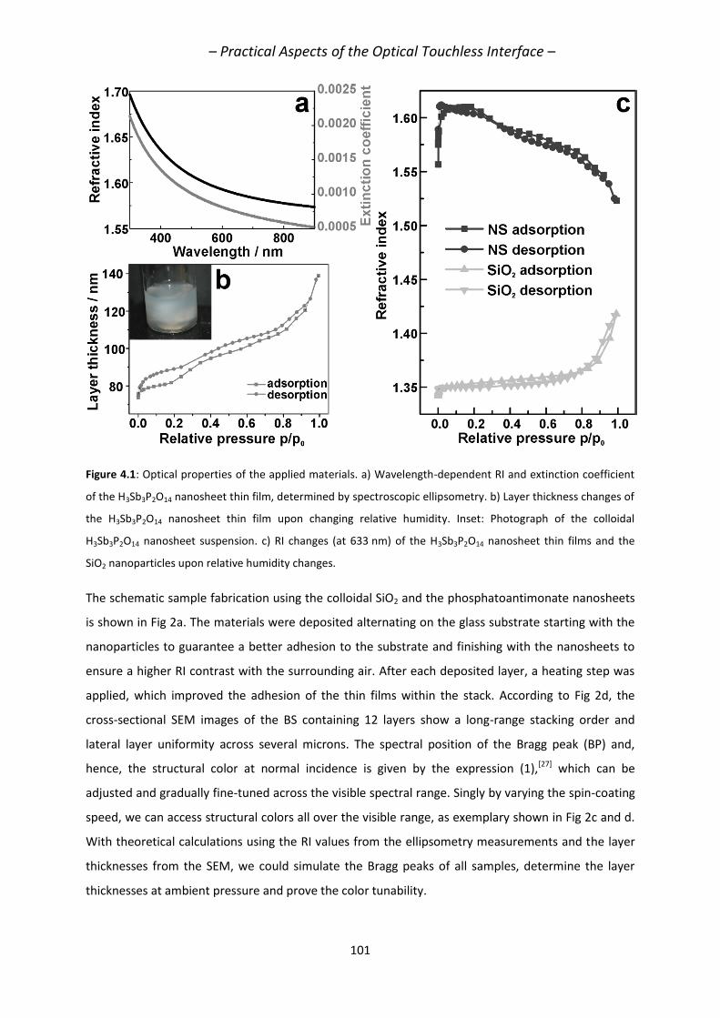
– Practical Aspects of the Optical Touchless Interface –
101
Figure 4.1: Optical properties of the applied materials. a) Wavelength-dependent RI and extinction coefficient
of the H3Sb3P2O14 nanosheet thin film, determined by spectroscopic ellipsometry. b) Layer thickness changes of
the H3Sb3P2O14 nanosheet thin film upon changing relative humidity. Inset: Photograph of the colloidal
H3Sb3P2O14 nanosheet suspension. c) RI changes (at 633 nm) of the H3Sb3P2O14 nanosheet thin films and the
SiO2 nanoparticles upon relative humidity changes.
The schematic sample fabrication using the colloidal SiO2 and the phosphatoantimonate nanosheets
is shown in Fig 2a. The materials were deposited alternating on the glass substrate starting with the
nanoparticles to guarantee a better adhesion to the substrate and finishing with the nanosheets to
ensure a higher RI contrast with the surrounding air. After each deposited layer, a heating step was
applied, which improved the adhesion of the thin films within the stack. According to Fig 2d, the
cross-sectional SEM images of the BS containing 12 layers show a long-range stacking order and
lateral layer uniformity across several microns. The spectral position of the Bragg peak (BP) and,
hence, the structural color at normal incidence is given by the expression (1),[27] which can be
adjusted and gradually fine-tuned across the visible spectral range. Singly by varying the spin-coating
speed, we can access structural colors all over the visible range, as exemplary shown in Fig 2c and d.
With theoretical calculations using the RI values from the ellipsometry measurements and the layer
thicknesses from the SEM, we could simulate the Bragg peaks of all samples, determine the layer
thicknesses at ambient pressure and prove the color tunability.
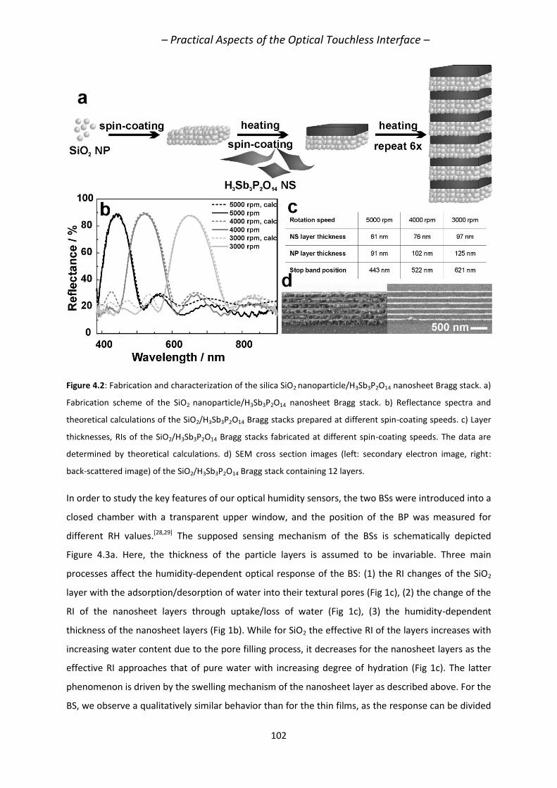
– Practical Aspects of the Optical Touchless Interface –
102
Figure 4.2: Fabrication and characterization of the silica SiO2 nanoparticle/H3Sb3P2O14 nanosheet Bragg stack. a)
Fabrication scheme of the SiO2 nanoparticle/H3Sb3P2O14 nanosheet Bragg stack. b) Reflectance spectra and
theoretical calculations of the SiO2/H3Sb3P2O14 Bragg stacks prepared at different spin-coating speeds. c) Layer
thicknesses, RIs of the SiO2/H3Sb3P2O14 Bragg stacks fabricated at different spin-coating speeds. The data are
determined by theoretical calculations. d) SEM cross section images (left: secondary electron image, right:
back-scattered image) of the SiO2/H3Sb3P2O14 Bragg stack containing 12 layers.
In order to study the key features of our optical humidity sensors, the two BSs were introduced into a
closed chamber with a transparent upper window, and the position of the BP was measured for
different RH values.[28,29] The supposed sensing mechanism of the BSs is schematically depicted
Figure 4.3a. Here, the thickness of the particle layers is assumed to be invariable. Three main
processes affect the humidity-dependent optical response of the BS: (1) the RI changes of the SiO2
layer with the adsorption/desorption of water into their textural pores (Fig 1c), (2) the change of the
RI of the nanosheet layers through uptake/loss of water (Fig 1c), (3) the humidity-dependent
thickness of the nanosheet layers (Fig 1b). While for SiO2 the effective RI of the layers increases with
increasing water content due to the pore filling process, it decreases for the nanosheet layers as the
effective RI approaches that of pure water with increasing degree of hydration (Fig 1c). The latter
phenomenon is driven by the swelling mechanism of the nanosheet layer as described above. For the
BS, we observe a qualitatively similar behavior than for the thin films, as the response can be divided
– Practical Aspects of the Optical Touchless Interface –
103
into two RH ranges, the low range 0-90% and the high range 90-100%.The photonic stop band
redshifts by 100 nm in the lower RH range (up to 90%) as plotted in Fig 3b. This shift is accompanied
by a gradual reflectance intensity decrease, which finally vanishes (Fig 3b, light gray spectrum), the
color of the BS switches off, i.e. becomes completely transparent. This effect finds its explanation in
the elimination of the RI contrast between the layers forming the BS with increasing RH (Fig 1c).
While the RI of the particle layer increases, the RI of the nanosheet layer decreases while the layer
thickness increases, leading to an overall redshift of the BP. Since the RIs of the nanosheet and
nanoparticle layers follow opposite trends, the difference becomes sufficiently low at above 95% RH,
leading to the disappearance of the optical contrast. As the BP is canceled out, the optical sensor
turns completely transparent and light is transmitted by the structure throughout the visible range.
Transparency switching through reversible RI matching has previously been realized by rational
porosity tuning and RI tailoring of the constituent layers.[30,31] These hygrochromic multilayers
however are only capable of detecting liquid water, rather than humidity changes.
To obtain another important key feature of these ultrasensitive humidity sensors, the selectivity was
tested. For this, we placed the sensors into a closed atmosphere and the ethanol relative pressure
was raised, while the optical response of the system was detected. According to Fig 3c, we observe a
total shift of around 50 nm, which is escorted by a gradual reflectance intensity decrease of 10%. The
trends are similar to the trend observed upon humidity adsorption, but the magnitude of the
changes is smaller. As the nanoparticle layer presents only the optical contrast material and a gate to
ensure the infiltration over the whole structure, the selectivity is presumably given by the nanosheet
layers. Taking this into account, the different optical response to the two analytes is determined by
the intercalation degree. We assume that due to size effects, only a lower intercalation degree of
ethanol molecules in the interlayer space is favorable. This lower intercalation rate means a smaller
layer thickness increase and also a smaller RI decrease. The RI contrast is not cancelled out
completely and the structural color and a photonic stop band are present over the whole ethanol
relative pressure range. With these two qualitatively similar but quantitatively different behavior we
could demonstrate the selectivity to humidity against ethanol vapor.
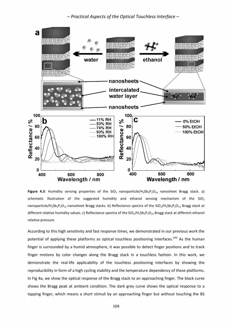
– Practical Aspects of the Optical Touchless Interface –
104
Figure 4.3: Humidity sensing properties of the SiO2 nanoparticle/H3Sb3P2O14 nanosheet Bragg stack. a)
schematic illustration of the suggested humidity and ethanol sensing mechanism of the SiO2
nanoparticle/H3Sb3P2O14 nanosheet Bragg stacks. b) Reflectance spectra of the SiO2/H3Sb3P2O14 Bragg stack at
different relative humidity values. c) Reflectance spectra of the SiO2/H3Sb3P2O14 Bragg stack at different ethanol
relative pressure.
According to this high sensitivity and fast response times, we demonstrated in our previous work the
potential of applying these platforms as optical touchless positioning interfaces.[26] As the human
finger is surrounded by a humid atmosphere, it was possible to detect finger positions and to track
finger motions by color changes along the Bragg stack in a touchless fashion. In this work, we
demonstrate the real-life applicability of the touchless positioning interfaces by showing the
reproducibility in form of a high cycling stability and the temperature dependency of these platforms.
In Fig 4a, we show the optical response of the Bragg stack to an approaching finger. The black curve
shows the Bragg peak at ambient condition. The dark grey curve shows the optical response to a
tapping finger, which means a short stimuli by an approaching finger but without touching the BS
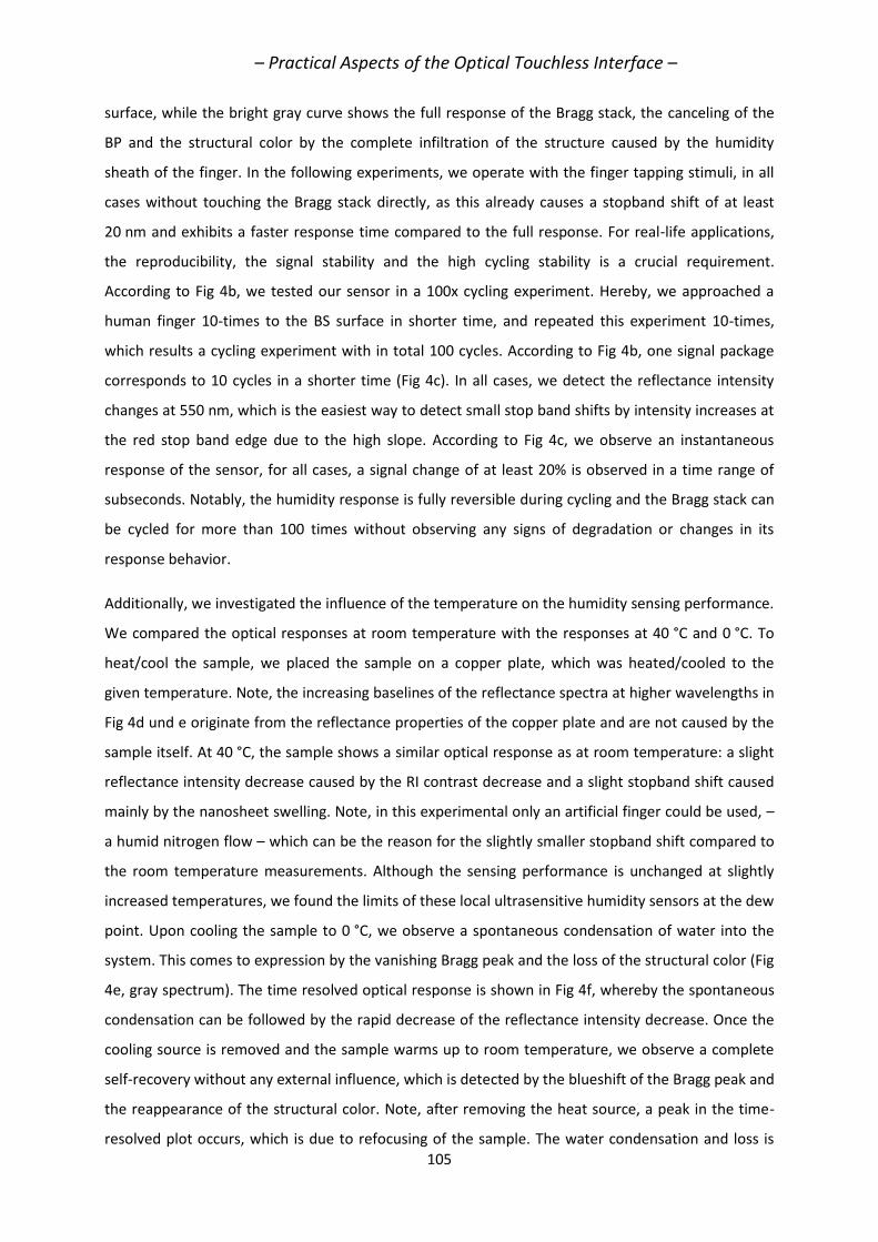
– Practical Aspects of the Optical Touchless Interface –
105
surface, while the bright gray curve shows the full response of the Bragg stack, the canceling of the
BP and the structural color by the complete infiltration of the structure caused by the humidity
sheath of the finger. In the following experiments, we operate with the finger tapping stimuli, in all
cases without touching the Bragg stack directly, as this already causes a stopband shift of at least
20 nm and exhibits a faster response time compared to the full response. For real-life applications,
the reproducibility, the signal stability and the high cycling stability is a crucial requirement.
According to Fig 4b, we tested our sensor in a 100x cycling experiment. Hereby, we approached a
human finger 10-times to the BS surface in shorter time, and repeated this experiment 10-times,
which results a cycling experiment with in total 100 cycles. According to Fig 4b, one signal package
corresponds to 10 cycles in a shorter time (Fig 4c). In all cases, we detect the reflectance intensity
changes at 550 nm, which is the easiest way to detect small stop band shifts by intensity increases at
the red stop band edge due to the high slope. According to Fig 4c, we observe an instantaneous
response of the sensor, for all cases, a signal change of at least 20% is observed in a time range of
subseconds. Notably, the humidity response is fully reversible during cycling and the Bragg stack can
be cycled for more than 100 times without observing any signs of degradation or changes in its
response behavior.
Additionally, we investigated the influence of the temperature on the humidity sensing performance.
We compared the optical responses at room temperature with the responses at 40 °C and 0 °C. To
heat/cool the sample, we placed the sample on a copper plate, which was heated/cooled to the
given temperature. Note, the increasing baselines of the reflectance spectra at higher wavelengths in
Fig 4d und e originate from the reflectance properties of the copper plate and are not caused by the
sample itself. At 40 °C, the sample shows a similar optical response as at room temperature: a slight
reflectance intensity decrease caused by the RI contrast decrease and a slight stopband shift caused
mainly by the nanosheet swelling. Note, in this experimental only an artificial finger could be used, –
a humid nitrogen flow – which can be the reason for the slightly smaller stopband shift compared to
the room temperature measurements. Although the sensing performance is unchanged at slightly
increased temperatures, we found the limits of these local ultrasensitive humidity sensors at the dew
point. Upon cooling the sample to 0 °C, we observe a spontaneous condensation of water into the
system. This comes to expression by the vanishing Bragg peak and the loss of the structural color (Fig
4e, gray spectrum). The time resolved optical response is shown in Fig 4f, whereby the spontaneous
condensation can be followed by the rapid decrease of the reflectance intensity decrease. Once the
cooling source is removed and the sample warms up to room temperature, we observe a complete
self-recovery without any external influence, which is detected by the blueshift of the Bragg peak and
the reappearance of the structural color. Note, after removing the heat source, a peak in the time-
resolved plot occurs, which is due to refocusing of the sample. The water condensation and loss is
– Practical Aspects of the Optical Touchless Interface –
106
completely reversible and could be repeated several times (not shown). Therefore, we propose that
the spontaneous condensation at 0°C and the local sensitivity to humidity changes can be utilized for
other applications, such as a photonic dew point sensor. We would like to note, however, that in real
life, devices such as smartphones or touchscreens in general are heated by internal electrics and/or
Joule heating to well above 0°C, even if the surrounding temperatures are lower. For this reason, the
condensation of humidity from the atmosphere can be avoided and the water uptake and loss is fully
reversible. Therefore, we do not expect major problems if the external temperature decreases to and
below 0°C, but the operation temperature of the possible device should be above the dew point.
Figure 4.4: Optical touchless positioning interface tested at different temperatures. a) Reflectance spectra of
the silica SiO2 nanoparticle/H3Sb3P2O14 nanosheet Bragg stack showing witout a finger, with a full-finger stimuli
and with a tapping finger stimuli. b) Time resolved response of the SiO2/H3Sb3P2O14 Bragg stack in a 100x
cycling experiment. c) Magnification of one “signal package” of 10 cyclings. For one cycle, a finger “tapping”
experiment was used in which a human finger was only shortly approached to the SiO2/H3Sb3P2O14 Bragg stack
surface. In such a “tapping experiment” a reflectance intensity change of at least 20% is observed. d)
Reflectance spectra of the SiO2/H3Sb3P2O14 Bragg stack at 40 °C without a finger and at tapping stimuli. e)
Reflectance spectra of the SiO2/H3Sb3P2O14 Bragg stack at 0 °C without a finger and at tapping stimuli. f) Time
resolved response of the SiO2/H3Sb3P2O14 Bragg stack upon cooling the sample from room temperature to 0 °C.
In conclusion, we studied the optical properties and the sensing performance of 2D
phosophatoantimonate nanosheets. Hereby, we determined the complex RI depending on the
wavelength via spectroscopic ellipsometry and showed the evolution of the RI and the layer
thickness of thin films depending of the relative humidity. Observing massive changes in these two
– Practical Aspects of the Optical Touchless Interface –
107
properties, we integrated these 2D nanosheets into Bragg stacks, which show besides the high
sensitivity to humidity changes, a high selectivity to water against ethanol vapor. Finally, we
investigated further properties of our previously published optical touchless positioning interface.
Hereby we proved the high reversibility, signal stability and reproducibility, the influence of the
temperatures, whereby the natural limits of these humidity sensing devices were detected to be at
the dew point.
4.6 EXPERIMENTAL
Solid state synthesis, protonation and exfoliation of nanosheets
For the synthesis of K3Sb3P2O14 the precursors (KNO3 (99 %, Merck), Sb2O3 (99.6 %, Alfa Aesar),
NH4H2PO4 (98 %+, Acros Organics)) were thoroughly ground in a stoichiometric ratio and heated up in
a two-step solid state synthesis as described elsewhere.[32] For the proton exchange reaction, 2 g of
K3Sb3P2O14 were treated with 250 mL of 8 M nitric acid (diluted 65 wt%, Merck) overnight, filtrated,
washed with ethanol and dried at room temperature. For a complete exchange reaction, this was
repeated once. Exfoliation was carried out by stirring the H3Sb3P2O14 vigorously overnight in pure
water with a concentration of bulk protons of 7.3 mmol L-1.[26] The obtained colloidal suspensions
were centrifuged at 3000 rpm for 30 min to remove agglomerates and non-exfoliated bulk material.
To obtain the nanosheet pellet, an additional centrifugation step was applied at 18000 rpm for
30 min. The supernatant was discarded and the gel-like colourless wet aggregate was dried at 100 °C.
Preparation of colloidal suspensions
The dried colorless precipitate of the water exfoliated H3Sb3P2O14 nanosheets was redispersed with a
concentration of 42 mmol L-1 in a water/ethanol mixture (60 vol% ethanol) and sonicated for 2 h. The
The commercial colloids of SiO2 (LUDOX TMA, Sigma) were redispersed at 3 wt% in methanol and
sonicated for 15 min.
Fabrication of thin films and Bragg stacks
All films were fabricated by spin-coating (WS-650S-NPP-Lite, Laurell Technologies Corporation) using
concentrations given above. Different film thicknesses were accessed by varying the spin-coating
speed, which allows the fine-tuning of the optical properties.[13] On plasma cleaned glass slides
(2.5 cm x 2.5 cm), 400 µl of the colloidal suspensions were spin-coated alternatingly for 1 min with a
defined speed (2000 rpm, 3000 rpm and 4000 rpm were applied, a constant speed within one BS),
and heated to 80 °C for 15 min after each layer deposition. Other parameters such as colloidal
concentration, spin-coating time and acceleration rate were kept constant.
– Practical Aspects of the Optical Touchless Interface –
108
Characterization
SEM cross-sectional images of the Bragg stacks were taken with a Zeiss Merlin FE-SEM.
All reflectance spectra were measured with a fiber optic spectrometer (USB2000+, Ocean Optics)
attached to a microscope (DM2500, Leica) with normal incidence and the reflectance spectra were
always taken at the same spot (1×1 mm2 in area). To obtain the optical changes with relative
humidity change, the Bragg stacks were kept in a stainless steel chamber with a total volume of 5 mL,
placed above 0.7 mL of the saturated salt solutions[5,6] at around 25 °C in a closed stainless steel
chamber with a transparent glass window. At each step, 20 min atmosphere equilibration time was
needed. In the ethanol vapor sorption measurements, the BSs were placed into a closed chamber
with the dimensions of 2.5x2.5x0.5 cm3, where well-defined relative analyte relative pressure values
were realized by connecting the inserted pipette tip with a liquid-gas flow controller (Bronkhorst)
and a vaporizer (CEM) with a massflow-controlled carrier gas flow. To observe a specific relative
pressure, the carrier gas nitrogen (200 mL min-1) and the liquid analyte were dosed into the CEM
(controlled evaporation and mixing, W101A-130-K, Bronkhorst High-Tech),[8] where the thermal
evaporation of the analyte took place. The CEM was heated to temperatures above the boiling point.
The relative vapor pressures were calculated via the software FLUIDAT (CEM calculation), which
considers the actual atmospheric pressure, the temperature and the properties of the analyte, such
as vapor pressure and heat capacity.[33] The obtained data were analyzed with the SPECTRA SUITE
software.
Porosimetry measurements were carried out by the porosimetry tool of Sopra PS-1000 SAM,
whereby the sample was equilibrated at all vapor relative pressures values for 15 min. The
measurement results were fitted with the software Sopra SAE using the model combination Cauchy
and Lorentz. The thickness of the SiO2 layers was considered as unchanged and only the RI was fitted
over the relative pressure range. For the nanosheet thin films both values, the layer thickness and
also the RI were fitted. Before all measurements, the nanoparticle samples were heated for 30 min
to 200 °C and the nanosheets thin films for 30 min to 60 °C in vacuum to remove the atmospheric
water from pores and between the nanosheets. To obtain the optical isotherms, all fitted
measurement results were plotted against the analyte relative pressure.
Touchless positioning interface measurements
To test the reproducibility of the touchless positioning interfaces, cycling experiments was carried
out by finger tapping experiments by approaching (but not touching) and distancing the finger in
regular intervals of ca. 30 s. This measurement was used to determine the response time of the
Bragg stack, which was defined as the time it takes for 90% of the stopband shift before the
– Practical Aspects of the Optical Touchless Interface –
109
structural color vanishes. To detect the stopband changes, the intensity changes at the wavelength
550 nm were followed. To test the temperature dependency, the optical response was tested at 40°C
and 0°C and was compared to room temperature. Hereby, the BS was heated/cooled via a copper
plate and an approaching finger was used as stimuli.
4.7 REFERENCES
[1] S. John, Phys. Rev. Lett. 1987, 58, 2486-2489.
[2] E. Yablonovitch, Phys. Rev. Lett. 1987, 58, 2059-2062.
[3] J. R. C. Smirnov, M. Ito, M. E. Calvo, C. López-López, A. Jiménez-Solano, J. F. Galisteo-López, P.
Zavala-Rivera, K. Tanaka, E. Sivaniah, H. Míguez, Adv. Opt. Mater. 2015, 3, 1633-1639.
[4] N. Hidalgo, M. E. Calvo, H. Míguez, Small 2009, 5, 2309-2315.
[5] O. Sanchez-Sobrado, M. E. Calvo, H. Miguez, J. Mater. Chem. 2010, 20, 8240-8246.
[6] L. D. Bonifacio, D. P. Puzzo, S. Breslav, B. M. Willey, A. McGeer, G. A. Ozin, Adv. Mater. 2010, 22,
1351-1354.
[7] L. D. Bonifacio, G. A. Ozin, A. C. Arsenault, Small 2011, 7, 3153-3157.
[8] T. L. Kelly, A. Garcia Sega, M. J. Sailor, Nano Lett. 2011, 11, 3169-3173.
[9] K. P. Raymond, I. B. Burgess, M. H. Kinney, M. Loncar, J. Aizenberg, Lab Chip 2012, 12, 3666-
3669.
[10] A. T. Exner, I. Pavlichenko, D. Baierl, M. Schmidt, G. Derondeau, B. V. Lotsch, P. Lugli, G. Scarpa,
Laser Phot. Rev. 2014, 5, 726-733.
[11] I. Pavlichenko, E. Broda, Y. Fukuda, K. Szendrei, A. K. Hatz, G. Scarpa, P. Lugli, C. Brauchle, B. V.
Lotsch, Mater. Horiz. 2015, 2, 299-308.
[12] B. V. Lotsch, G. A. Ozin, J. Am.Chem. Soc. 2008, 130, 15252-15253.
[13] B. V. Lotsch, G. A. Ozin, ACS Nano 2008, 2, 2065-2074.
[14] B. V. Lotsch, F. Scotognella, K. Moeller, T. Bein, G. A. Ozin, SPIE, 7713, Vol. 7713, 2010, p. 7713V.
[15] M. E. Calvo, O. Sánchez-Sobrado, S. Colodrero, H. Míguez, Langmuir 2009, 25, 2443-2448.
[16] L. D. Bonifacio, B. V. Lotsch, D. P. Puzzo, F. Scotognella, G. A. Ozin, Adv. Mater. 2009, 21,
1641-1646.
[17] J. D. Joannopoulos, S. G. Johnson, J. N. Winn, R. D. Meade, Photonic crystals: molding the flow of
light, Princeton university press, 2011.
[18] I. Pavlichenko, A. T. Exner, M. Guehl, P. Lugli, G. Scarpa, B. V. Lotsch, J. Phys. Chem. C 2011, 116,
298-305.
[19] C. Fenzl, T. Hirsch, O. S. Wolfbeis, Angew. Chem. Int. Ed. 2014, 53, 3318-3335.
[20] F. M. Hinterholzinger, A. Ranft, J. M. Feckl, B. Ruhle, T. Bein, B. V. Lotsch, J. Mater. Chem. 2012,
22, 10356-10362.
– Practical Aspects of the Optical Touchless Interface –
110
[21] A. Ranft, F. Niekiel, I. Pavlichenko, N. Stock, B. V. Lotsch, Chem. Mater. 2015, 27, 1961–1970.
[22] Z. Wang, J. Zhang, J. Xie, C. Li, Y. Li, S. Liang, Z. Tian, T. Wang, H. Zhang, H. Li, W. Xu, B. Yang, Adv.
Funct. Mater. 2010, 20, 3784-3790.
[23] Y. Kang, J. J. Walish, T. Gorishnyy, E. L. Thomas, Nat. Mater. 2007, 6, 957-960.
[24] A. C. Arsenault, D. P. Puzzo, I. Manners, G. A. Ozin, Nat. Photonics 2007, 1, 468-472.
[25] S. Deniard-Courant, Y. Piffard, P. Barboux, J. Livage, Solid State Ionics 1988, 27, 189-194.
[26] J.-C. P. Gabriel, F. Camerel, B. J. Lemalre, H. Desvaux, P. Davidson, P. Batail, Nature 2001, 413,
504-508.
[27] F. Camerel, J. C. P. Gabriel, P. Batail, P. Panine, P. Davidson, Langmuir 2003, 19, 10028-10035.
[28] K. Szendrei, P. Ganter, O. Sánchez-Sobrado, R. Eger, A. Kuhn, B. V. Lotsch, Adv. Mater. 2015, 27,
6341-6348.
[29] S. Joannopoulos, J. N. Winn, R. D. Meade, Photonic crystals: molding the flow of light, Princeton
University press, 2008, 2nd edition, 4.
[30] P. W. Winston, D. H. Bates, Ecology 1960, 41, 232-237.
[31] L. Greenspan, J. Res. Nat. Bur. Stand. 1977, 81A, 89-96.
[32] M. N. Ghazzal, O. Deparis, J. De Coninck, E. M. Gaigneaux, J. Mater. Chem. C 2013, 1, 6202-6209.
[33] K. E. Shopsowitz, H. Qi, W. Y. Hamad, M. J. MacLachlan, Nature 2010, 468, 422-425.
[34] Y. Piffard, A. Lachgar, M. Tournoux, J. Solid State Chem. 1985, 58, 253-256.
[35] Bronkhorst High-Tech, www.fluidat.com, accessed: 06-12/2014.
– Optical Vapor Differentiation –
111
5. TAILORING THE SENSOR`S
SELECTIVITY:
OPTICAL DISCRIMINATION OF DIFFERENT SOLVENTS
BY 2D NANOSHEET BASED 1D PHOTONIC CRYSTALS
5.1 SUMMARY
The development of single-component sensors with high
sensitivity and selectivity is one of the key challenges in sensor
design. In addition, the ability of a sensor to distinguish between
chemically similar analytes usually requires either
multicomponent sensor arrays or sophisticated device
fabrication, combined with complex statistical data processing
such as principal component analysis, to enhance the selectivity.
In this project, we address these aspects by introducing another
member of the antimony phosphate nanosheet family, HSbP2O8 as highly chemo-selective
components in thin-film based sensors, which operate based on either resistive or optical read-out.
The main difference between the previously presented nanosheets (H3Sb3P2O14) and the here
presented HSbP2O8 lies in the crystal structure: while H3Sb3P2O14 shows inherent pores in the
nanosheet layer itself, HSbP2O8 nanosheets are dense and the analyte diffusion is limited to
pathways along the grain boundaries, which turned out to be relevant for the sensor’s selectivity.
Similar to H3Sb3P2O14 nanosheets, the high sensitivity of HSbP2O8 nanosheets towards water vapor is
given by the intercalation of the water molecules into the interlayer space, causing significant
swelling, which translates into structural color changes when the nanosheets are integrated into
1DPC architectures. Not only full-spectrum stopband shifts with a fast response time were shown in
this project, but also the response to other volatile organic compounds (VOCs) is of interest. By
comparing the saturation times and the photonic stopband shifts for different VOCs, we could
optically distinguish between non-protic (polar and non-polar) and protic solvent vapors. Due to
different interactions and intercalation rates of the analytes, protic analytes showed slow response
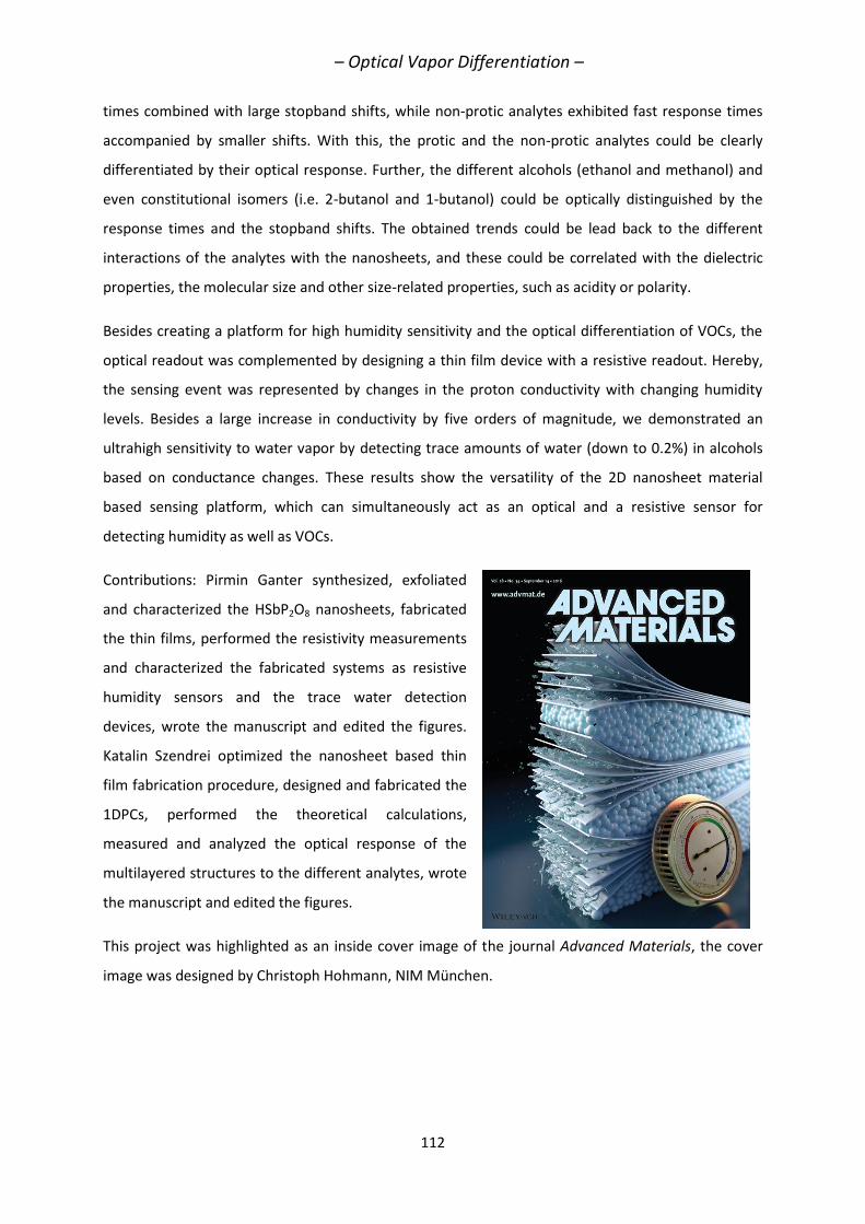
– Optical Vapor Differentiation –
112
times combined with large stopband shifts, while non-protic analytes exhibited fast response times
accompanied by smaller shifts. With this, the protic and the non-protic analytes could be clearly
differentiated by their optical response. Further, the different alcohols (ethanol and methanol) and
even constitutional isomers (i.e. 2-butanol and 1-butanol) could be optically distinguished by the
response times and the stopband shifts. The obtained trends could be lead back to the different
interactions of the analytes with the nanosheets, and these could be correlated with the dielectric
properties, the molecular size and other size-related properties, such as acidity or polarity.
Besides creating a platform for high humidity sensitivity and the optical differentiation of VOCs, the
optical readout was complemented by designing a thin film device with a resistive readout. Hereby,
the sensing event was represented by changes in the proton conductivity with changing humidity
levels. Besides a large increase in conductivity by five orders of magnitude, we demonstrated an
ultrahigh sensitivity to water vapor by detecting trace amounts of water (down to 0.2%) in alcohols
based on conductance changes. These results show the versatility of the 2D nanosheet material
based sensing platform, which can simultaneously act as an optical and a resistive sensor for
detecting humidity as well as VOCs.
Contributions: Pirmin Ganter synthesized, exfoliated
and characterized the HSbP2O8 nanosheets, fabricated
the thin films, performed the resistivity measurements
and characterized the fabricated systems as resistive
humidity sensors and the trace water detection
devices, wrote the manuscript and edited the figures.
Katalin Szendrei optimized the nanosheet based thin
film fabrication procedure, designed and fabricated the
1DPCs, performed the theoretical calculations,
measured and analyzed the optical response of the
multilayered structures to the different analytes, wrote
the manuscript and edited the figures.
This project was highlighted as an inside cover image of the journal Advanced Materials, the cover
image was designed by Christoph Hohmann, NIM München.
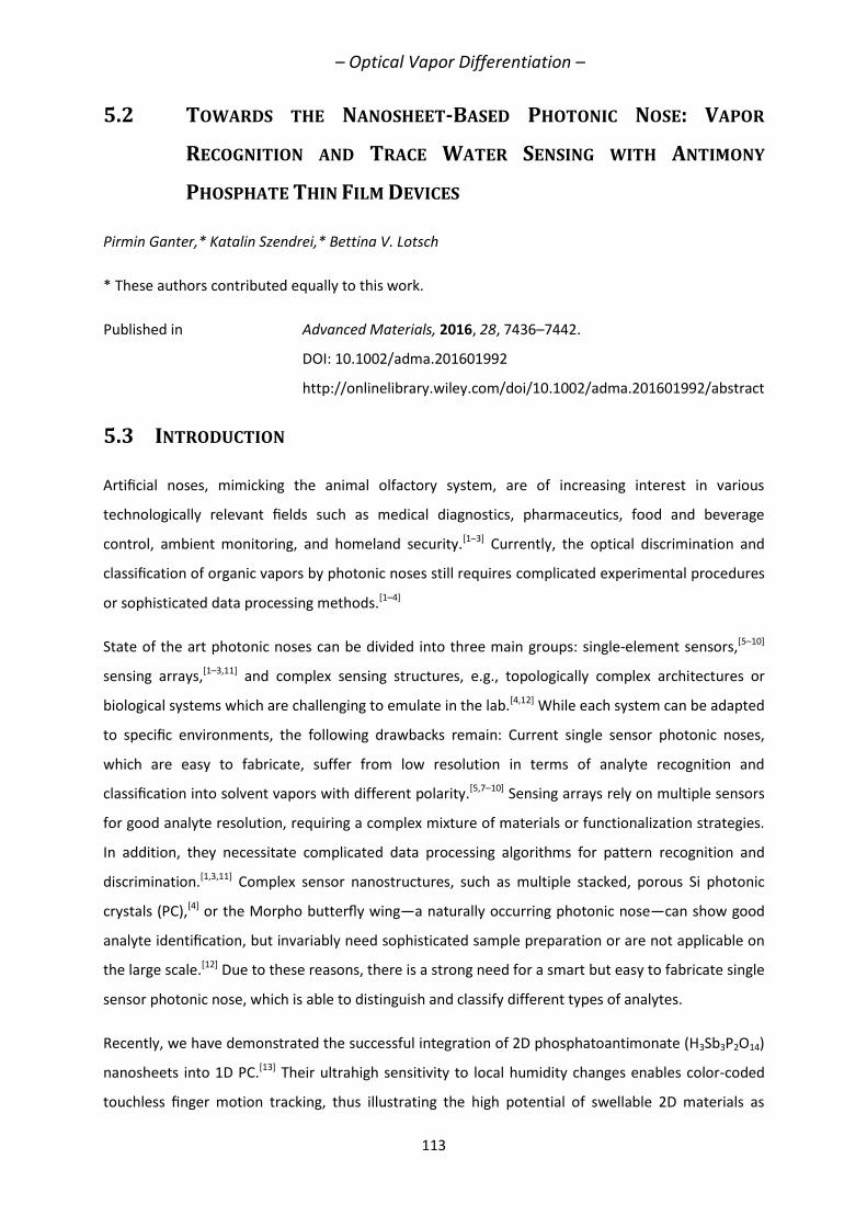
– Optical Vapor Differentiation –
113
5.2 TOWARDS THE NANOSHEET-BASED PHOTONIC NOSE: VAPOR
RECOGNITION AND TRACE WATER SENSING WITH ANTIMONY
PHOSPHATE THIN FILM DEVICES
Pirmin Ganter,* Katalin Szendrei,* Bettina V. Lotsch
* These authors contributed equally to this work.
Published in Advanced Materials, 2016, 28, 7436–7442.
DOI: 10.1002/adma.201601992
http://onlinelibrary.wiley.com/doi/10.1002/adma.201601992/abstract
5.3 INTRODUCTION
Artificial noses, mimicking the animal olfactory system, are of increasing interest in various
technologically relevant fields such as medical diagnostics, pharmaceutics, food and beverage
control, ambient monitoring, and homeland security.[1–3] Currently, the optical discrimination and
classification of organic vapors by photonic noses still requires complicated experimental procedures
or sophisticated data processing methods.[1–4]
State of the art photonic noses can be divided into three main groups: single-element sensors,[5–10]
sensing arrays,[1–3,11] and complex sensing structures, e.g., topologically complex architectures or
biological systems which are challenging to emulate in the lab.[4,12] While each system can be adapted
to specific environments, the following drawbacks remain: Current single sensor photonic noses,
which are easy to fabricate, suffer from low resolution in terms of analyte recognition and
classification into solvent vapors with different polarity.[5,7–10] Sensing arrays rely on multiple sensors
for good analyte resolution, requiring a complex mixture of materials or functionalization strategies.
In addition, they necessitate complicated data processing algorithms for pattern recognition and
discrimination.[1,3,11] Complex sensor nanostructures, such as multiple stacked, porous Si photonic
crystals (PC),[4] or the Morpho butterfly wing—a naturally occurring photonic nose—can show good
analyte identification, but invariably need sophisticated sample preparation or are not applicable on
the large scale.[12] Due to these reasons, there is a strong need for a smart but easy to fabricate single
sensor photonic nose, which is able to distinguish and classify different types of analytes.
Recently, we have demonstrated the successful integration of 2D phosphatoantimonate (H3Sb3P2O14)
nanosheets into 1D PC.[13] Their ultrahigh sensitivity to local humidity changes enables color-coded
touchless finger motion tracking, thus illustrating the high potential of swellable 2D materials as
– Optical Vapor Differentiation –
114
active sensing components in photonic nanostructures. To demonstrate the generality of this
approach and to highlight the potential of an intercalative sensing mechanism for analyte
discrimination, we here introduce a new type of stimuli responsive 2D material, namely HSbP2O8
antimony phosphate nanosheets.
Similar to H3Sb3P2O14, HSbP2O8 as a bulk material has extraordinary swelling properties, [14] which
have been used to produce nematic liquid crystalline phases in water. [15] In contrast to H3Sb3P2O14,
HSbP2O8 loses water completely at zero humidity, hence making it a superior sensor candidate owing
to its higher sensitivity in this humidity regime.[14,16]The reason for the incomplete water loss of
H3Sb3P2O14 can be rationalized by the presence of structural pores which can host water molecules,
while the layers in HSbP2O8 are dense. The highly polar and acidic interlayer environment of HSbP2O8,
its high sensitivity at low relative humidity[14,16] and the generally higher sensitivity of nanosheets
compared to their bulk materials[13,17,18] renders HSbP2O8 nanosheet-based thin film devices
promising candidates for tracking trace amounts of water as well as for the discrimination of organic
vapors.
Here, we report the first comprehensive characterization of HSbP2O8 2D nanosheets and
demonstrate their outstanding sensitivity to humidity—especially in the low humidity range. Based
on these features, we develop resistive thin film sensors that are able to detect even trace amounts
of water in alcohols. We then exploit the unique film forming capability of the 2D nanosheets to
develop highly sensitive photonic crystal sensors which can identify various organic vapors with high
accuracy, which is superior to all other single-component photonic vapor sensing structures reported
to date.[5-10]
5.4 RESULTS AND DISCUSSION
KSbP2O8was synthesized by a solid-state reaction starting from KNO3, Sb2O3, and NH4H2PO4 and
protonated with 8 M HNO3 (Figures S5.1 and S 5.2, and Table S 5.1, Supporting Information).[14,15,19,20]
The antimony phosphate and its corresponding solid acid consist of anionic 2D SbP2O8-sheets
separated by charge compensating cations which occupy the interlayer space (Figure S 5.3,
Supporting Information).[19,20] The hexagonal crystal habit of HSbP2O8 is shown in Figure 5.1a. Upon
exfoliation with pure water (Figure S 5.4, Supporting Information), the morphology becomes “silk-
like” (Figure 5.1b, Figure S 5.5, Supporting Information), indicating successful delamination.
Exfoliation into single layer nanosheets was further confirmed by various analytical techniques (see
Figures 5.1, Figures S 5.6, S 5.7, and S 5.8, and Tables S 5.2 and S 5.3, Supporting Information). The
thickness of a single nanosheet was determined to be 0.9 0.1 nm by atomic force microscopy
(AFM) (Figure 5.1 d), which agrees well with the crystallographic single layer thickness of 0.66 nm.[21]
– Optical Vapor Differentiation –
115
The high aspect ratio and film texture can be clearly seen by transmission electron microscopy (TEM)
(Figure 5.1 e). The selected area electron diffraction (SAD) pattern of an individual nanosheet
(Figure 5.1 e inset) exhibits d -values that are in excellent agreement with those obtained from
powder X-ray diffraction measurements (see Table S 5.2, Supporting Information, and Figure 5.1 c)
illustrating the structural in-plane integrity. Rietveld refinement of the diffraction pattern of a
precipitated nanosheet pellet, showing a characteristic Warren-type peak profile (Figure 5.1 c)
evidences the turbostratically disordered nanosheet arrangement.
Large area thin films were prepared by spin-coating nanosheets from the colloidal suspension and
investigated by thin film X-ray diffraction (Figure S 5.9, Supporting Information) and by ellipsometric
porosimetry (Figure S 5.10, Supporting Information). Only the 00l reflections were observed in the
out ofplane XRD pattern pointing toward a parallel orientation of the nanosheets to the surface of
the substrate. Upon exposure to moisture, the thin film swells to almost double its thickness. The
swelling of the film is caused by intercalation of water molecules between the turbostratically
disordered nanosheets and into the resulting grain boundaries. The refractive index (RI) n decreases
from 1.57 to 1.50 with increasing humidity as the film becomes more “water-like” with increasing
water uptake. Water uptake was also monitored by the Raman spectra of the bulk material as well as
the nanosheet pellet (Figure S 5.11, Supporting Information). Slight changes are observed by the
emergence of a band at 482 cm-1 (Sb O···P stretching vibration) and by narrowing of the terminal P-O
stretching vibration at 1270 cm-1. The latter band is sensitive to water uptake as the P-O bond points
toward the interlayer space in which water is intercalated.
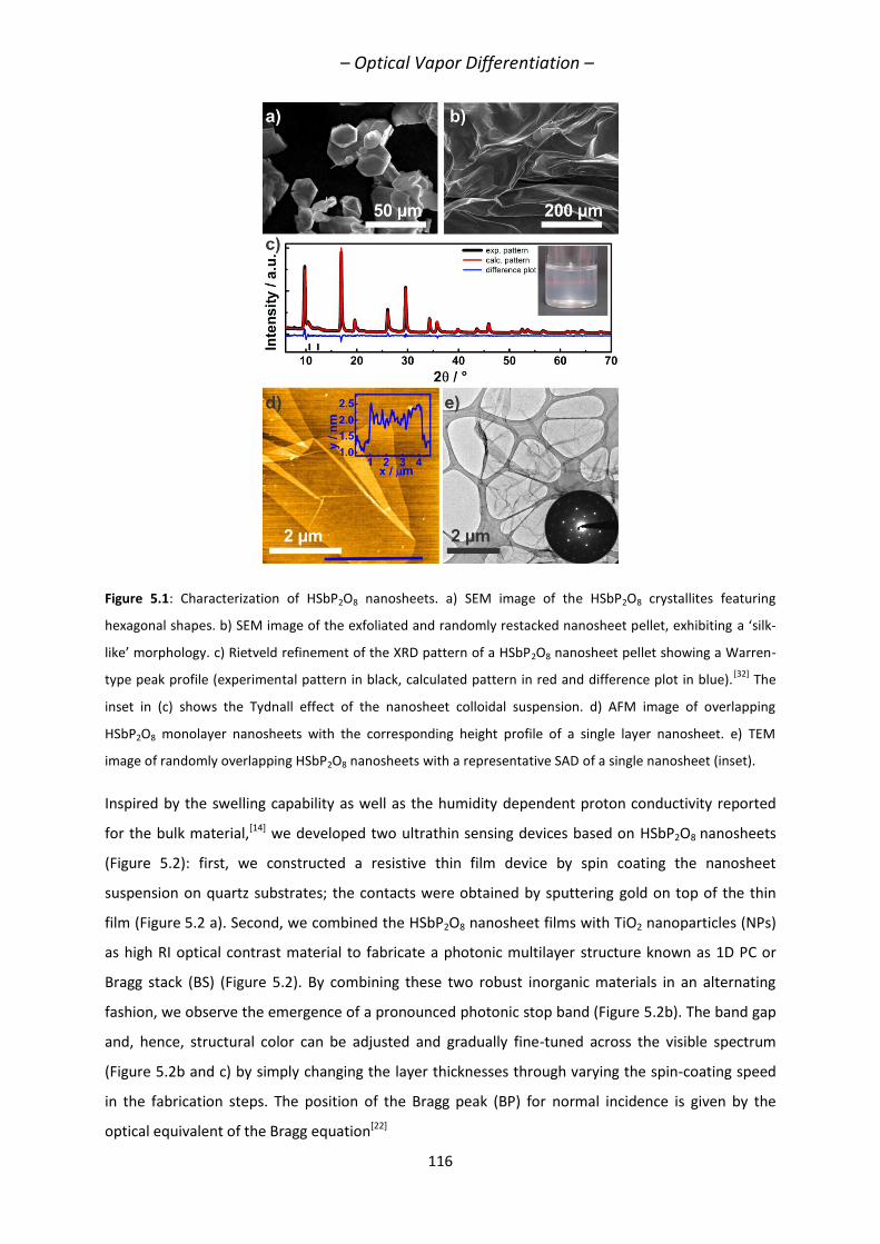
– Optical Vapor Differentiation –
116
Figure 5.1: Characterization of HSbP2O8 nanosheets. a) SEM image of the HSbP2O8 crystallites featuring
hexagonal shapes. b) SEM image of the exfoliated and randomly restacked nanosheet pellet, exhibiting a ‘silk-
like’ morphology. c) Rietveld refinement of the XRD pattern of a HSbP2O8 nanosheet pellet showing a Warren-
type peak profile (experimental pattern in black, calculated pattern in red and difference plot in blue).[32]
The
inset in (c) shows the Tydnall effect of the nanosheet colloidal suspension. d) AFM image of overlapping
HSbP2O8 monolayer nanosheets with the corresponding height profile of a single layer nanosheet. e) TEM
image of randomly overlapping HSbP2O8 nanosheets with a representative SAD of a single nanosheet (inset).
Inspired by the swelling capability as well as the humidity dependent proton conductivity reported
for the bulk material,[14] we developed two ultrathin sensing devices based on HSbP2O8 nanosheets
(Figure 5.2): first, we constructed a resistive thin film device by spin coating the nanosheet
suspension on quartz substrates; the contacts were obtained by sputtering gold on top of the thin
film (Figure 5.2 a). Second, we combined the HSbP2O8 nanosheet films with TiO2 nanoparticles (NPs)
as high RI optical contrast material to fabricate a photonic multilayer structure known as 1D PC or
Bragg stack (BS) (Figure 5.2). By combining these two robust inorganic materials in an alternating
fashion, we observe the emergence of a pronounced photonic stop band (Figure 5.2b). The band gap
and, hence, structural color can be adjusted and gradually fine-tuned across the visible spectrum
(Figure 5.2b and c) by simply changing the layer thicknesses through varying the spin-coating speed
in the fabrication steps. The position of the Bragg peak (BP) for normal incidence is given by the
optical equivalent of the Bragg equation[22]
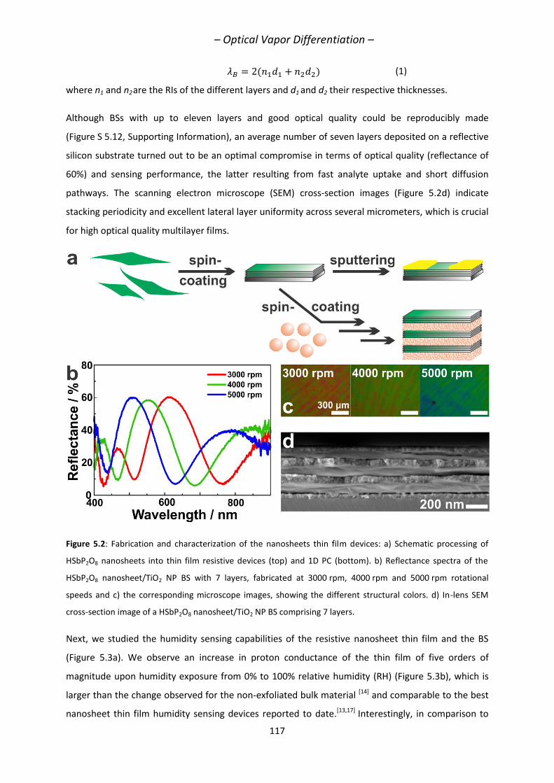
– Optical Vapor Differentiation –
117
(1)
where n1 and n2 are the RIs of the different layers and d1 and d2 their respective thicknesses.
Although BSs with up to eleven layers and good optical quality could be reproducibly made
(Figure S 5.12, Supporting Information), an average number of seven layers deposited on a reflective
silicon substrate turned out to be an optimal compromise in terms of optical quality (reflectance of
60%) and sensing performance, the latter resulting from fast analyte uptake and short diffusion
pathways. The scanning electron microscope (SEM) cross-section images (Figure 5.2d) indicate
stacking periodicity and excellent lateral layer uniformity across several micrometers, which is crucial
for high optical quality multilayer films.
Figure 5.2: Fabrication and characterization of the nanosheets thin film devices: a) Schematic processing of
HSbP2O8 nanosheets into thin film resistive devices (top) and 1D PC (bottom). b) Reflectance spectra of the
HSbP2O8 nanosheet/TiO2 NP BS with 7 layers, fabricated at 3000 rpm, 4000 rpm and 5000 rpm rotational
speeds and c) the corresponding microscope images, showing the different structural colors. d) In-lens SEM
cross-section image of a HSbP2O8 nanosheet/TiO2 NP BS comprising 7 layers.
Next, we studied the humidity sensing capabilities of the resistive nanosheet thin film and the BS
(Figure 5.3a). We observe an increase in proton conductance of the thin film of five orders of
magnitude upon humidity exposure from 0% to 100% relative humidity (RH) (Figure 5.3b), which is
larger than the change observed for the non-exfoliated bulk material [14] and comparable to the best
nanosheet thin film humidity sensing devices reported to date.[13,17] Interestingly, in comparison to
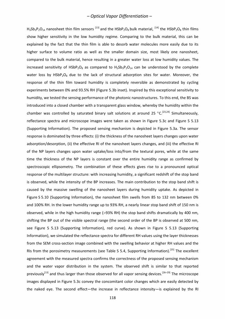
– Optical Vapor Differentiation –
118
H3Sb3P2O14 nanosheet thin film sensors [13] and the HSbP2O8 bulk material, [14] the HSbP2O8 thin films
show higher sensitivity in the low humidity regime. Comparing to the bulk material, this can be
explained by the fact that the thin film is able to desorb water molecules more easily due to its
higher surface to volume ratio as well as the smaller domain size, most likely one nanosheet,
compared to the bulk material, hence resulting in a greater water loss at low humidity values. The
increased sensitivity of HSbP2O8 as compared to H3Sb3P2O14 can be understood by the complete
water loss by HSbP2O8 due to the lack of structural adsorption sites for water. Moreover, the
response of the thin film toward humidity is completely reversible as demonstrated by cycling
experiments between 0% and 93.5% RH (Figure 5.3b inset). Inspired by this exceptional sensitivity to
humidity, we tested the sensing performance of the photonic nanostructures. To this end, the BS was
introduced into a closed chamber with a transparent glass window, whereby the humidity within the
chamber was controlled by saturated binary salt solutions at around 25 C.[23,24] Simultaneously,
reflectance spectra and microscope images were taken as shown in Figure 5.3c and Figure S 5.13
(Supporting Information). The proposed sensing mechanism is depicted in Figure 5.3a. The sensor
response is dominated by three effects: (i) the thickness of the nanosheet layers changes upon water
adsorption/desorption, (ii) the effective RI of the nanosheet layers changes, and (iii) the effective RI
of the NP layers changes upon water uptake/loss into/from the textural pores, while at the same
time the thickness of the NP layers is constant over the entire humidity range as confirmed by
spectroscopic ellipsometry. The combination of these effects gives rise to a pronounced optical
response of the multilayer structure: with increasing humidity, a significant redshift of the stop band
is observed, while the intensity of the BP increases. The main contribution to the stop band shift is
caused by the massive swelling of the nanosheet layers during humidity uptake. As depicted in
Figure S 5.10 (Supporting Information), the nanosheet film swells from 85 to 132 nm between 0%
and 100% RH. In the lower humidity range up to 93% RH, a nearly linear stop band shift of 150 nm is
observed, while in the high humidity range (93% RH) the stop band shifts dramatically by 400 nm,
shifting the BP out of the visible spectral range (the second order of the BP is observed at 500 nm,
see Figure S 5.13 (Supporting Information), red curve). As shown in Figure S 5.13 (Supporting
Information), we simulated the reflectance spectra for different RH values using the layer thicknesses
from the SEM cross-section image combined with the swelling behavior at higher RH values and the
RIs from the porosimetry measurements (see Table S 5.4, Supporting Information).[25] The excellent
agreement with the measured spectra confirms the correctness of the proposed sensing mechanism
and the water vapor distribution in the system. The observed shift is similar to that reported
previously[13] and thus larger than those observed for all vapor sensing devices.[26–29] The microscope
images displayed in Figure 5.3c convey the concomitant color changes which are easily detected by
the naked eye. The second effect—the increase in reflectance intensity—is explained by the RI
– Optical Vapor Differentiation –
119
changes upon water uptake: while the RI of the NP layers increases (from 1.84 to 1.96) by filling the
textural pores (Figure S 5.14, Supporting Information), the RI of the nanosheet layer decreases (from
1.56 to 1.50) by water intercalation. These opposite trends induce an increase in the RI contrast and,
hence, in the reflectivity of the multilayer system at increasing humidity levels (Figure S 5.13,
Supporting Information).
Besides sensitivity, another important performance parameter for sensors is the response time,
defined as the time which is needed to reach 90% of the stop band shift between 0% and 100% RH.
The fast response time of 23 s (Figure S 5.15, Supporting Information), which is superior to most
existing humidity sensing devices with a large signal resolution based on a swelling mechanism,[26–29]
again underlines the applicability of these platforms for practical humidity sensing. It is important to
note in this context that the time response of the reflectance intensity change represented by its
time derivative (Figure S 5.15, Supporting Information) is instantaneous and so is the associated
optical response: humidity changes cause an immediate stop band shift, which translates into an
ultrafast increase or decrease in reflectance intensity at the observed wavelength within seconds
(see inset of Figure S 5.15, Supporting Information). Other important sensor properties such as
long-term stability and cycling stability were tested by applying a 2-month-old sample in a multiple
cycling experiment (shown in Figure S 5.15, Supporting Information). As a result, the sensing
performance (stop band shift and response time) was found unchanged as compared to the freshly
prepared samples.
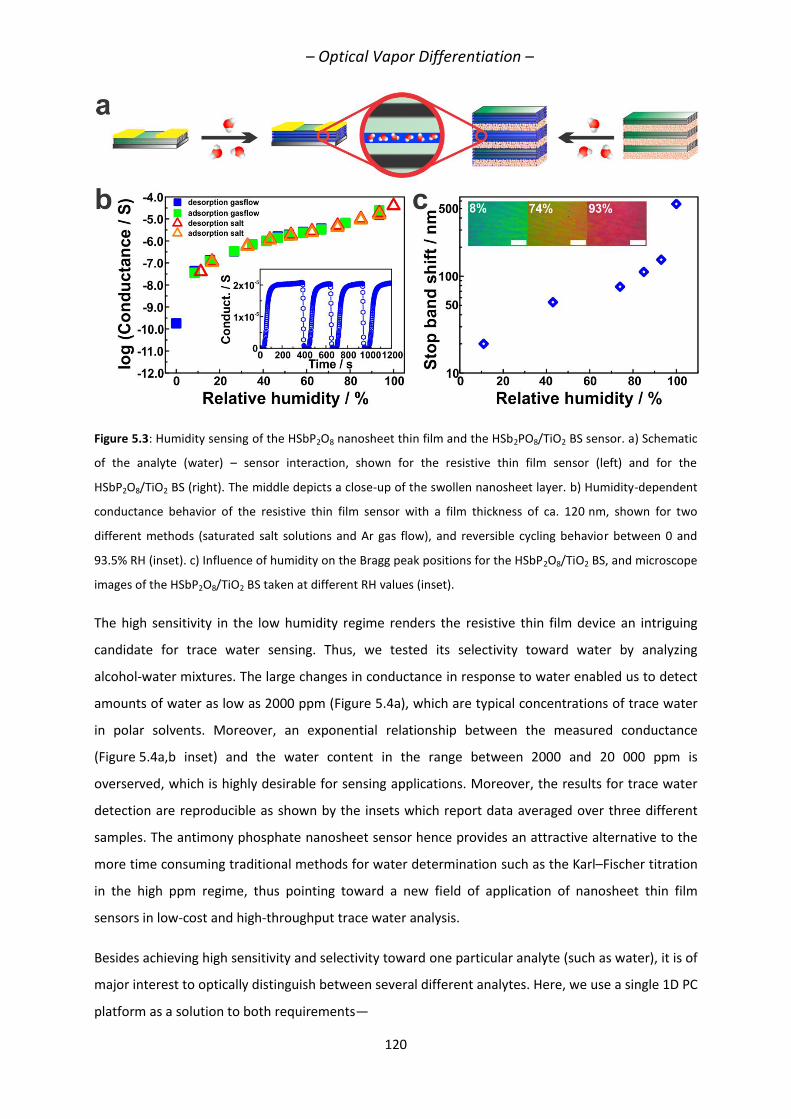
– Optical Vapor Differentiation –
120
Figure 5.3: Humidity sensing of the HSbP2O8 nanosheet thin film and the HSb2PO8/TiO2 BS sensor. a) Schematic
of the analyte (water) – sensor interaction, shown for the resistive thin film sensor (left) and for the
HSbP2O8/TiO2 BS (right). The middle depicts a close-up of the swollen nanosheet layer. b) Humidity-dependent
conductance behavior of the resistive thin film sensor with a film thickness of ca. 120 nm, shown for two
different methods (saturated salt solutions and Ar gas flow), and reversible cycling behavior between 0 and
93.5% RH (inset). c) Influence of humidity on the Bragg peak positions for the HSbP2O8/TiO2 BS, and microscope
images of the HSbP2O8/TiO2 BS taken at different RH values (inset).
The high sensitivity in the low humidity regime renders the resistive thin film device an intriguing
candidate for trace water sensing. Thus, we tested its selectivity toward water by analyzing
alcohol-water mixtures. The large changes in conductance in response to water enabled us to detect
amounts of water as low as 2000 ppm (Figure 5.4a), which are typical concentrations of trace water
in polar solvents. Moreover, an exponential relationship between the measured conductance
(Figure 5.4a,b inset) and the water content in the range between 2000 and 20 000 ppm is
overserved, which is highly desirable for sensing applications. Moreover, the results for trace water
detection are reproducible as shown by the insets which report data averaged over three different
samples. The antimony phosphate nanosheet sensor hence provides an attractive alternative to the
more time consuming traditional methods for water determination such as the Karl–Fischer titration
in the high ppm regime, thus pointing toward a new field of application of nanosheet thin film
sensors in low-cost and high-throughput trace water analysis.
Besides achieving high sensitivity and selectivity toward one particular analyte (such as water), it is of
major interest to optically distinguish between several different analytes. Here, we use a single 1D PC
platform as a solution to both requirements—
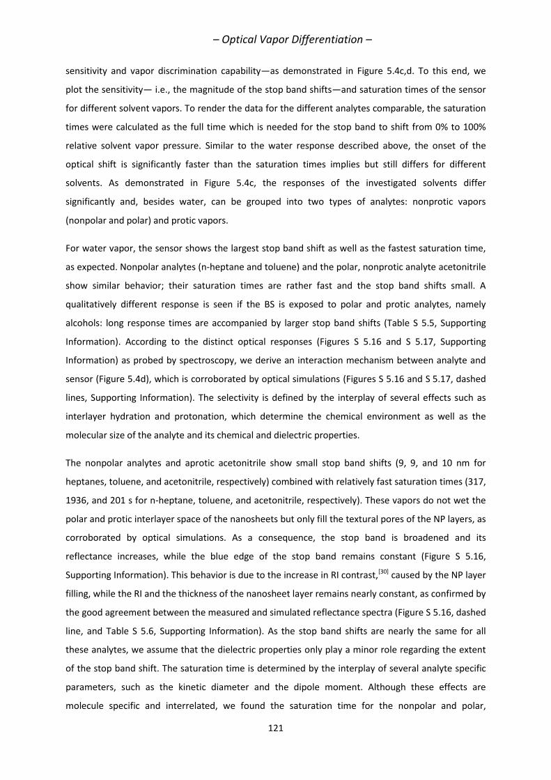
– Optical Vapor Differentiation –
121
sensitivity and vapor discrimination capability—as demonstrated in Figure 5.4c,d. To this end, we
plot the sensitivity— i.e., the magnitude of the stop band shifts—and saturation times of the sensor
for different solvent vapors. To render the data for the different analytes comparable, the saturation
times were calculated as the full time which is needed for the stop band to shift from 0% to 100%
relative solvent vapor pressure. Similar to the water response described above, the onset of the
optical shift is significantly faster than the saturation times implies but still differs for different
solvents. As demonstrated in Figure 5.4c, the responses of the investigated solvents differ
significantly and, besides water, can be grouped into two types of analytes: nonprotic vapors
(nonpolar and polar) and protic vapors.
For water vapor, the sensor shows the largest stop band shift as well as the fastest saturation time,
as expected. Nonpolar analytes (n-heptane and toluene) and the polar, nonprotic analyte acetonitrile
show similar behavior; their saturation times are rather fast and the stop band shifts small. A
qualitatively different response is seen if the BS is exposed to polar and protic analytes, namely
alcohols: long response times are accompanied by larger stop band shifts (Table S 5.5, Supporting
Information). According to the distinct optical responses (Figures S 5.16 and S 5.17, Supporting
Information) as probed by spectroscopy, we derive an interaction mechanism between analyte and
sensor (Figure 5.4d), which is corroborated by optical simulations (Figures S 5.16 and S 5.17, dashed
lines, Supporting Information). The selectivity is defined by the interplay of several effects such as
interlayer hydration and protonation, which determine the chemical environment as well as the
molecular size of the analyte and its chemical and dielectric properties.
The nonpolar analytes and aprotic acetonitrile show small stop band shifts (9, 9, and 10 nm for
heptanes, toluene, and acetonitrile, respectively) combined with relatively fast saturation times (317,
1936, and 201 s for n-heptane, toluene, and acetonitrile, respectively). These vapors do not wet the
polar and protic interlayer space of the nanosheets but only fill the textural pores of the NP layers, as
corroborated by optical simulations. As a consequence, the stop band is broadened and its
reflectance increases, while the blue edge of the stop band remains constant (Figure S 5.16,
Supporting Information). This behavior is due to the increase in RI contrast,[30] caused by the NP layer
filling, while the RI and the thickness of the nanosheet layer remains nearly constant, as confirmed by
the good agreement between the measured and simulated reflectance spectra (Figure S 5.16, dashed
line, and Table S 5.6, Supporting Information). As the stop band shifts are nearly the same for all
these analytes, we assume that the dielectric properties only play a minor role regarding the extent
of the stop band shift. The saturation time is determined by the interplay of several analyte specific
parameters, such as the kinetic diameter and the dipole moment. Although these effects are
molecule specific and interrelated, we found the saturation time for the nonpolar and polar,
– Optical Vapor Differentiation –
122
nonprotic analytes to correlate most clearly with the kinetic diameter of the molecules
(Figures S 5.18 and S 5.19, Supporting Information): increasing saturation times correlate with the
increasing molecular sizes and the resulting delayed diffusion of toluene (1936 s, 6.1 Å) compared to
n-heptane (317 s, 4.3 Å) and acetonitrile (201 s, 3.4 Å).
In contrast, the optical response of the BS to protic solvent vapors—alcohols—signifi cantly differs
from that seen for aprotic analytes. Here, rather large stop band shifts were detected across the
series methanol (33 nm) < ethanol (58 nm) < 2-propanol (120 nm) < 1-propanol (132 nm) < 2-butanol
(150 nm) < 1-butanol (170 nm), with slow response times increasing in the following order: methanol
(897 s) < ethanol (3130 s) < 1-propanol (4043 s) < 1-butanol (9320 s) < 2-propanol (12 140 s) < 2-
butanol (≈70 000 s). In all cases, larger stop band shifts are observed compared to the stop band
broadening for nonprotic vapors (nonpolar vapors and acetonitrile). Contrary to the nonprotic
analytes, however, the color shift is dominated by changes in the nanosheet layer thickness upon
analyte infiltration, as evidenced by ellipsometric porosimetry and as exemplarily shown for ethanol
(Figure S 5.20, Supporting Information): the protic character of the analytes allows for stronger
interactions with the protic interlayer space and causes layer swelling upon intercalation. Further, we
analyzed the time-dependent stop band changes and could distinguish two different phases during
vapor sorption (Figure S 5.21, Supporting Information). Within the first ≈6 s, we observe a fast
response expressed by a broadening of the stop band, accompanied by an increase in reflectance,
similar to the overall response observed for the nonprotic analytes. We attribute this initial behavior
to the filling of the more easily accessible porous NP layers. In a second stage, a slower, analyte-
specific response is observed, corresponding to a distinct stop band shift and giving rise to the
analyte-specific saturation time, which is due to the intercalation of the analyte into the nanosheet
layer. According to this time-dependent behavior, we clearly see that the rate-limiting step is
associated with the intercalation of the analytes between the nanosheet layers, while the infiltration
of the NP layers is rather fast, as shown also for the nonprotic solvents as well as for water vapor.
This interpretation is in line with rather weak interactions of the NP layer and the analytes, which is
expected since no surface functionalization was carried out and the diffusion through a mesoporous
layer is generally rather fast.[31] To understand the sensing mechanism, which for the alcohols is
dominated by the nanosheet layer–analyte interaction, we investigate the influence of several
parameters on the stop band shift, such as the analyte’s kinetic diameter, dipole moment, dielectric
constant, and the RI. These parameters give rise to the analyte’s dielectric, optical, and
physicochemical properties such as its polarity and ability to form hydrogen bonds. The stop band
shift and the saturation times most obviously correlate with the analyte’s kinetic diameter, whereby
we could confirm by optical simulations that the layer thickness swelling is increasing with increasing
molecular sizes (Table S 5.6, Supporting Information). However, empirical correlations can be found
– Optical Vapor Differentiation –
123
as well for the dielectric constant and the RI of the analytes (Figures S 5.18 and S 5.19, Supporting
Information). In summary, although the above parameters are interrelated and most likely their
complex interplay determines the stop band shift, it is this interplay that is distinct for each individual
analyte, hence giving rise to an analyte-specific response.
It is of note that even constitutional isomers, e.g., those of propanol and butanol, can be
distinguished by our nanosheet based photonic nose. The saturation time is increased for 2-propanol
compared to 1-propanol by a factor of 3 (12 140 s vs 4043 s), and for 2-butanol compared to 1-
butanol by a factor 7 (≈70 000 s vs 9320 s), whereby the stop band shifts are comparable for both
isomers (132 nm vs 120 nm and 170 nm vs 150 nm). Although the kinetic diameters for both isomers
are similar, subtle differences in the molecular shape and polarity may have a significant effect on
the analyte’s interaction with the nanosheet layers and, hence, its diffusivity, which is reflected in the
signifycantly different saturation times. Overall, while the degree of swelling caused by the two
isomers is similar, a differentiation of both constitutional isomers is clearly possible through the
saturation times. Note that the reproducibility of the sensor response was verified by measuring
each solvent vapor three times. The error bars in Figure 5.4c are testament to the high
reproducibility and the ability of our system to reliably discriminate between different solvent
vapors.
In addition, we studied the sensor performance for analyzing multiple component mixtures. For
water–ethanol mixtures (Figure S 5.22, Supporting Information) we find that with increasing water
amount in the mixture the stop band shifts also increase. With this, the relative amount of water in a
water–ethanol mixture can be reliably determined by evaluating the stop band shift, which is as large
as 80 nm for water contents between 0% and 90% (Figure S 5.22 b–e, Supporting Information).
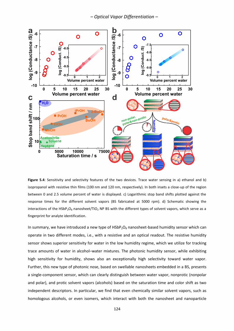
– Optical Vapor Differentiation –
124
Figure 5.4: Sensitivity and selectivity features of the two devices. Trace water sensing in a) ethanol and b)
isopropanol with resistive thin films (100 nm and 120 nm, respectively). In both insets a close-up of the region
between 0 and 2.5 volume percent of water is displayed. c) Logarithmic stop band shifts plotted against the
response times for the different solvent vapors (BS fabricated at 5000 rpm). d) Schematic showing the
interactions of the HSbP2O8 nanosheet/TiO2 NP BS with the different types of solvent vapors, which serve as a
fingerprint for analyte identification.
In summary, we have introduced a new type of HSbP2O8 nanosheet-based humidity sensor which can
operate in two different modes, i.e., with a resistive and an optical readout. The resistive humidity
sensor shows superior sensitivity for water in the low humidity regime, which we utilize for tracking
trace amounts of water in alcohol–water mixtures. The photonic humidity sensor, while exhibiting
high sensitivity for humidity, shows also an exceptionally high selectivity toward water vapor.
Further, this new type of photonic nose, based on swellable nanosheets embedded in a BS, presents
a single-component sensor, which can clearly distinguish between water vapor, nonprotic (nonpolar
and polar), and protic solvent vapors (alcohols) based on the saturation time and color shift as two
independent descriptors. In particular, we find that even chemically similar solvent vapors, such as
homologous alcohols, or even isomers, which interact with both the nanosheet and nanoparticle
– Optical Vapor Differentiation –
125
layers, can be reliably distinguished based on their sorption and diffusion characteristics. This single-
component sensor adds to a new generation of nanosheet sensing devices which operate based on
an interaction-driven, intercalative sensing mechanism that uniquely exploits both thermodynamic
and kinetic properties of the host–guest system, namely dispersive analyte-nanosheet interactions
and the diffusion properties of the analyte within the nanosheet layers. The rapidly increasing library
of accessible and chemically distinct nanosheet systems bodes well for the development of highly
analyte-specifi c colorimetric artificial noses, which opens up new possibilities in environmental
monitoring, trace water analysis, and biosensing.
5.5 ACKNOWLEDGEMENTS
Pirmin Ganter and Katalin Szendrei contributed equally to this work. Financial support was granted
by the Max Planck Society, the University of Munich (LMU), the Center for NanoScience (CeNS), and
the Deutsche Forschungsgemeinschaft (DFG) through the Cluster of Excellence Nanosystems
Initiative Munich (NIM). The authors thank Alexander Kuhn and Roland Eger for prior investigations
on the antimony phosphate system, Viola Duppel for TEM and SEM measurements, Claudia Kamella
for the EDX-SEM measurements, Willi Hölle for his technical support with the home-built argon flow
setup, and Bernhard Illes for contributing to the Bragg stack fabrication. Further, we thank Daniel
Selmeczi and the team of Semilab Sopra for their support with the ellipsometry measurements.
5.6 REFERENCES
[1] L. D. Bonifacio, D. P. Puzzo, S. Breslav, B. M. Willey, A. McGeer, G. A. Ozin, Adv. Mater. 2010,
22, 1351-1354.
[2] L. D. Bonifacio, G. A. Ozin, A. C. Arsenault, Small 2011, 7, 3153-3157.
[3] Z. Xie, K. Cao, Y. Zhao, L. Bai, H. Gu, H. Xu, Z.-Z. Gu, Adv. Mater. 2014, 26, 2413-2418.
[4] T. L. Kelly, A. Garcia Sega, M. J. Sailor, Nano Lett. 2011, 11, 3169-3173.
[5] A. Ranft, F. Niekiel, I. Pavlichenko, N. Stock, B. V. Lotsch, Chem. Mater. 2015, 27, 1961–1970.
[6] R. A. Potyrailo, H. Ghiradella, A. Vertiatchikh, K. Dovidenko, J. R. Cournoyer, E. Olson, Nat.
Photonics 2007, 1, 123-128.
[7] Y.-n. Wu, F. Li, W. Zhu, J. Cui, C.-a. Tao, C. Lin, P. M. Hannam, G. Li, Angew. Chem. Int. Ed.
2011, 50, 12518-12522.
[8] F. M. Hinterholzinger, A. Ranft, J. M. Feckl, B. Ruhle, T. Bein, B. V. Lotsch, J. Mater. Chem.
2012, 22, 10356-10362.
[9] C. Cui, Y. Liu, H. Xu, S. Li, W. Zhang, P. Cui, F. Huo, Small 2014, 10, 3672-3676.
[10] L. Li, X. Jiao, D. Chen, B. V. Lotsch, C. Li, Chem. Mater. 2015, 27, 7601-7609.
– Optical Vapor Differentiation –
126
[11] Y.-n. Wu, F. Li, Y. Xu, W. Zhu, C.-a. Tao, J. Cui, G. Li, Chem. Commun. 2011, 47, 10094-10096.
[12] Z. Hu, C.-a. Tao, F. Wang, X. Zou, J. Wang, J. Mater. Chem. C 2015, 3, 211-216.
[13] K. Szendrei, P. Ganter, O. Sànchez-Sobrado, R. Eger, A. Kuhn, B. V. Lotsch, Adv. Mater. 2015,
27, 6341-6348.
[14] S. Deniard-Courant, Y. Piffard, P. Barboux, J. Livage, Solid State Ionics 1988, 27, 189-194.
[15] N. Miura, H. Mizuno, N. Yamazoe, Jpn. J. Appl. Phys., Part 2 1988, 27, L931-L933.
[16] F. Camerel, J. C. P. Gabriel, P. Batail, P. Panine, P. Davidson, Langmuir 2003, 19, 10028-10035.
[17] S. Borini, R. White, D. Wei, M. Astley, S. Haque, E. Spigone, N. Harris, J. Kivioja, T. Ryhänen,
ACS Nano 2013, 7, 11166-11173.
[18] J. Feng, L. Peng, C. Wu, X. Sun, S. Hu, C. Lin, J. Dai, J. Yang, Y. Xie, Adv. Mater. 2012, 24,
1969-1974.
[19] Y. Piffard, S. Oyetola, S. Courant, A. Lachgar, J. Solid State Chem. 1985, 60, 209-213.
[20] Y. Piffard, A. Verbaere, S. Oyetola, S. Deniard-Courant, M. Tournoux, Eur. J. Solid State Inorg.
Chem. 1989, 26, 113-127.
[21] G. K. Prasad, N. Kumada, J. Yamanaka, Y. Yonesaki, T. Takei, N. Kinomura, J. Colloid Interface
Sci. 2006, 297, 654-659.
[22] J. D. Joannopoulos, S. G. Johnson, J. N. Winn, R. D. Meade, Photonic crystals: molding the
flow of light, Princeton university press, 2011.
[23] P. W. Winston, D. H. Bates, Ecology 1960, 41, 232-237.
[24] L. Greenspan, J. Res. Nat. Bur. Stand. 1977, 81A, 89-96.
[25] M. C. Fuertes, S. Colodrero, G. Lozano, A. R. González-Elipe, D. Grosso, C. Boissière, C.
Sánchez, G. J. d. A. A. Soler-Illia, H. Míguez, J. Phys. Chem. C 2008, 112, 3157-3163.
[26] E. Tian, J. Wang, Y. Zheng, Y. Song, L. Jiang, D. Zhu, J. Mater. Chem. 2008, 18, 1116-1122.
[27] J. H. Kim, J. H. Moon, S.-Y. Lee, J. Park, Appl. Phys. Lett. 2010, 97, 103701.
[28] Z. Wang, J. Zhang, J. Xie, C. Li, Y. Li, S. Liang, Z. Tian, T. Wang, H. Zhang, H. Li, W. Xu, B. Yang,
Adv. Funct. Mater. 2010, 20, 3784-3790.
[29] R. Xuan, Q. Wu, Y. Yin, J. Ge, J. Mater. Chem. 2011, 21, 3672-3676.
[30] L. D. Bonifacio, B. V. Lotsch, D. P. Puzzo, F. Scotognella, G. A. Ozin, Adv. Mater. 2009, 21,
1641-1646.
[31] I. Pavlichenko, E. Broda, Y. Fukuda, K. Szendrei, A. K. Hatz, G. Scarpa, P. Lugli, C. Brauchle, B.
V. Lotsch, Mater. Horiz. 2015, 2, 299-308.
[32] The two weak reflections marked with vertical scatters (Figure 5.1c) are stacking reflections
and result from non-complete preferred sample orientation. These peaks were fitted with a
single peak phase function
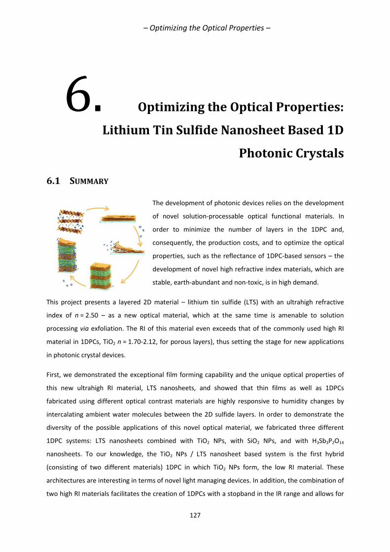
– Optimizing the Optical Properties –
127
6. Optimizing the Optical Properties:
Lithium Tin Sulfide Nanosheet Based 1D
Photonic Crystals
6.1 SUMMARY
The development of photonic devices relies on the development
of novel solution-processable optical functional materials. In
order to minimize the number of layers in the 1DPC and,
consequently, the production costs, and to optimize the optical
properties, such as the reflectance of 1DPC-based sensors – the
development of novel high refractive index materials, which are
stable, earth-abundant and non-toxic, is in high demand.
This project presents a layered 2D material – lithium tin sulfide (LTS) with an ultrahigh refractive
index of n = 2.50 – as a new optical material, which at the same time is amenable to solution
processing via exfoliation. The RI of this material even exceeds that of the commonly used high RI
material in 1DPCs, TiO2 n = 1.70-2.12, for porous layers), thus setting the stage for new applications
in photonic crystal devices.
First, we demonstrated the exceptional film forming capability and the unique optical properties of
this new ultrahigh RI material, LTS nanosheets, and showed that thin films as well as 1DPCs
fabricated using different optical contrast materials are highly responsive to humidity changes by
intercalating ambient water molecules between the 2D sulfide layers. In order to demonstrate the
diversity of the possible applications of this novel optical material, we fabricated three different
1DPC systems: LTS nanosheets combined with TiO2 NPs, with SiO2 NPs, and with H3Sb3P2O14
nanosheets. To our knowledge, the TiO2 NPs / LTS nanosheet based system is the first hybrid
(consisting of two different materials) 1DPC in which TiO2 NPs form, the low RI material. These
architectures are interesting in terms of novel light managing devices. In addition, the combination of
two high RI materials facilitates the creation of 1DPCs with a stopband in the IR range and allows for
– Optimizing the Optical Properties –
128
the reduction of the device thickness by as much as 60-65%, with obvious benefits for production
costs. Secondly, we introduced the highest RI contrast presented so far in the literature, to the best
of our knowledge, by combining SiO2 nanoparticles as a commonly used low RI material with LTS
nanosheets as the high RI material. These results are promising not only in terms of resource
efficiency and cost reduction, but also they directly entail relevant optical properties such as an
extremely broad bandwidth of the photonic stopband. Finally, we demonstrated the development of
highly sensitive humidity sensors by combining two nanosheet materials with individual ultrahigh
swelling capabilities – LTS nanosheets and H3Sb3P2O14 nanosheets – in a single 1DPC, rendering this
platform the first all-nanosheet 1DPC containing of two different simuli-responsive 2D materials. This
combination gives rise to ultralarge signal changes in response to changes in relative humidity and
opens the door to a new generation of high-performance humidity sensors.
Contributions: Katalin Szendrei-Temesi optimized the
LTS nanosheet based thin film fabrication procedure,
characterized the thin films, designed and fabricated
the 1DPCs, performed optical measurements and the
theoretical calculations, wrote the manuscript and
edited the figures. Olalla Sánchez-Sobrado fabricated
the first LTS nanosheet based thin films, proposed the
idea of the NP-based (SiO2 and TiO2) 1DPCs, fabricated
the initial Bragg stacks, helped writing the manuscript
and discussed the results. Sophia B. Betzler performed
the TEM-EELS measurements, assisted with writing the
manuscript and discussed the results. Katharina M.
Durner fabricated the multilayered structures and
performed some of the optical measurements. Tanja Holzmann designed some 3D images for the
figures, synthesized for the first time the LTS nanosheets, optimized the exfoliation and discussed the
results.
This project was highlighted as a back cover in the journal Advanced Functional Materials and the
cover image was designed by Katalin Szendrei-Temesi.
– Optimizing the Optical Properties –
129
6.2 LITHIUM TIN SULFIDE – A HIGH-REFRACTIVE-INDEX 2D MATERIAL
FOR HUMIDITY-RESPONSIVE PHOTONIC CRYSTALS
Katalin Szendrei-Temesi, Olalla Sanchez-Sobrado, Sophia Betzler, Katharina M. Durner, Tanja
Holzmann, Bettina V. Lotsch
Published in Advanced Functional Materials, 2018, 28, 1705740.
DOI: 10.1002/adfm.201705740
http://onlinelibrary.wiley.com/doi/10.1002/adfm.201705740/abstract
6.3 ABSTRACT
Extending the portfolio of novel stimuli-responsive, high-refractive-index (RI) materials besides
titania is key to improve the optical quality and sensing performance of existing photonic devices.
Herein, lithium tin sulfide (LTS) nanosheets are introduced as a novel solution processable ultrahigh
RI material (n = 2.50), which can be casted into homogeneous thin films using wet-chemical
deposition methods. Owing to its 2D morphology, thin films of LTS nanosheets are able to swell in
response to changes of relative humidity. Integration of LTS nanosheets into Bragg stacks (BSs) based
on TiO2, SiO2, nanoparticles or H3Sb3P2O14 nanosheets affords multilayer systems with high optical
quality at an extremely low device thickness of below 1 μm. Owing to the ultrahigh RI of LTS
nanosheets and the high transparency of the thin films, BSs based on porous titania as the low-RI
material are realized for the first time, showing potential application in light-managing devices.
Moreover, the highest RI contrast ever realized in BSs based on SiO2 and LTS nanosheets is reported.
Finally, exceptional swelling capability of an all-nanosheet BS based on LTS and H3Sb3P2O14
nanosheets is demonstrated, which bodes well for a new generation of humidity sensors with
extremely high sensitivity.
6.4 INTRODUCTION
New materials solutions are key for the development of novel sensing platforms with improved
optical properties and sensing performance compared to existing device concepts. One of the main
challenges in the development of photonic sensors is to identify high-refractive-index (RI) materials
which can easily be processed by wet-chemistry techniques and can be integrated into existing
device architectures. In addition, for an effective application in sensor technology, these materials
need to be stimuli responsive, which is typically achieved via inherent structural or textural porosity
or swelling behavior in the presence of analytes. The simplest photonic nanostructures used for
optical sensing applications, which are capable of translating external stimuli into an optical signal by
– Optimizing the Optical Properties –
130
structural color changes, are 1D photonic crystals (1D PCs), also referred to as Bragg stacks (BSs).[1,2]
BSs are composed of a high- and a low-RI material, which are stacked in an alternating fashion. The
periodic modulation of the RIs creates a photonic stopband: a forbidden energy range for photons
that are not allowed to propagate in the PC along certain directions in reciprocal space.[1] The
photonic stopband defines the structural color and is dependent on the layer thickness d and the RI n
of the constituent layers, given by the optical thickness τ= n · d.[3,4] By this means, dynamic variations
in the layer thickness or in the RI induced by an analyte can be translated into changes in the
stopband position and, hence, the structural color of the sensor.[5–12] The reflectance intensity—the
intensity of the photonic stopband—is mostly defined by the RI contrast, i.e., the RI difference
between the two materials.[2,3] Consequently, a high RI contrast results in devices with high
reflectance intensities and better optical qualities featuring a lower overall device thickness of well
below 1 µm.[13]
To create BSs with an ultrahigh RI contrast, high-RI materials are needed which preferably can be
deposited via straightforward wet-chemical methods such as spin- or dip-coating. The most
prominent candidate in the literature used as a high-RI material in BSs is titanium dioxide (TiO2),
which is applied either as a dense sol or as nanoparticles, forming a dense or a highly porous thin
film, respectively.[4,14,15] Although sol–gel-based dense TiO2 films or titania-based composite films
have a maximum RI of around n (dense) 2.12,[16–19] and n (composite) 2.38,[20] respectively,
volatile analytes cannot efficiently infiltrate the dense sol film, leading to significantly reduced or
even inhibited vapor responsiveness.[16,17] On the contrary, nanoparticulate TiO2 forms a highly
porous thin film through textural porosity, and mesopore filling can be monitored by optical
isotherms as a function of the relative pressure of the analyte.[7,16,21] Such porous TiO2 layers exhibit
an effective RI of n 1.70–2.00, depending on the degree of porosity.[5,14,15] Combined with SiO2
nanoparticles as the classical low-RI material, at least 10–12 layers are required to reach reflectance
intensities of 90%, resulting in rather thick devices of several micrometers. A strategy to reduce the
layer numbers and, hence, the device thickness, is the combination of highly porous SiO2 with dense
TiO2 films.[17–19] Although a high RI contrast and good optical device quality were achieved, the
sensitivity toward vapors is severely reduced due to the limited textural porosity of the titania layer.
Another approach to increase the RI contrast is to identify new porous materials with a similar or
even higher RI compared to TiO2, although current alternatives such as WO3 sol (n 2.03),[22] ZrO2
nanoparticles (n 1.70),[23,24] Ta2O5
[25] nanoparticles (n 1.80), undoped or antimony-doped SnO2
films (n (undoped) 1.83, n (3% Sbdoped) 2.34)[3,26] all feature lower RIs compared to dense titania
or suffer from low transparency in the visible range. Thus, the highest RI contrast BSs reported so far
combine highly
– Optimizing the Optical Properties –
131
porous silica layers stacked with dense titania layers, exhibiting an RI contrast of Δn 0.83,[17]
Δn 0.84,[19] and Δn 0.89.[18]
To further increase the RI contrast is an important objective when
aiming at high-quality optical devices, such as solar mirrors,[27] optical fibers,[28] or other
light-managing devices. All titania-based photonic structures employed for sensing feature textural
porosity in order to facilitate analyte diffusion. However, to achieve high sensitivity toward analytes,
swelling materials are preferred over porous materials as they cause larger stopband shifts via
changes in their optical thickness.[6,12,29,30] Thus, the combination of two different swelling materials in
one BS[31] is a promising strategy to induce ultralarge stopband shifts. To implement this strategy, the
development of novel functional nanomaterials featuring both high swelling capability and high RI is
one of the key challenges to be addressed.
Here, we present a new material platform for addressing both challenges: (i) we introduce a new
solution processable high-RI material—lithium tin sulfide (LTS) nanosheets[32,33] (n 2.50, 0% relative
humidity (RH), 633 nm)—which forms high-quality BSs with TiO2 as the low-RI material and produces
ultrahigh RI contrast in PCs when combined with a low-RI material such as silica; and (ii) we
demonstrate full-spectral color changes of an all-nanosheet BS composed of LTS and antimony
phosphate (H3Sb3P2O14) nanosheets. Taking advantage of the swelling capability of both 2D materials
in the presence of water vapor, such stimuli-responsive all-nanosheet BSs are promising candidates
for highly sensitive optical humidity sensors with good optical quality. The combination of two
robust, swellable nanosheet materials ensures both high stability, especially compared to flexible
organic materials, and presents a generic material platform that can be chemically tailored for
diverse applications in chemooptical sensing. In addition, the high RI contrast imparted by the
inorganic nanosheets, combined with their high sensitivity to humidity, ensures superior optical
quality combined with large signal changes, which makes LTS-based sensors competitive or even
superior to other state-of-the-art optical sensors.[34,35]
6.5 RESULTS AND DISCUSSION
Material synthesis
Layered bulk lithium tin sulfide (Li2Sn2S5) was synthesized by a classical solid-state reaction as
previously described.[32] The successful synthesis was confirmed by powder X-ray diffraction (XRD)
analysis, and the elemental composition was validated by energy-dispersive X-ray (EDX) and
inductively coupled plasma (ICP) analysis, as shown in Figure S 6.1 and Tables S 6.1 and S 6.2 in the
Supporting Information. The crystal structure consists of covalent layers of edge sharing SnS6
octahedra, whereby the Sn atoms are partially substituted by Li as depicted in Figure 6.1a.[33] The
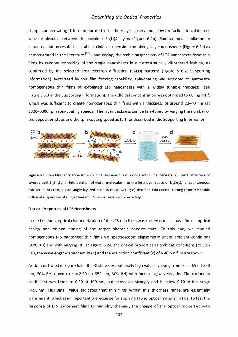
– Optimizing the Optical Properties –
132
charge-compensating Liions are located in the interlayer gallery and allow for facile intercalation of
water molecules between the covalent Sn(Li)S layers (Figure 6.2b). Spontaneous exfoliation in
aqueous solution results in a stable colloidal suspension containing single nanosheets (Figure 6.1c) as
demonstrated in the literature.[32] Upon drying, the stable suspensions of LTS nanosheets form thin
films by random restacking of the single nanosheets in a turbostratically disordered fashion, as
confirmed by the selected area electron diffraction (SAED) patterns (Figure S 6.2, Supporting
Information). Motivated by this film forming capability, spin-coating was explored to synthesize
homogeneous thin films of exfoliated LTS nanosheets with a widely tunable thickness (see
Figure S 6.3 in the Supporting Information). The colloidal concentration was optimized to 60 mg mL-1,
which was sufficient to create homogeneous thin films with a thickness of around 20–40 nm (at
3000–5000 rpm spin-coating speeds). The layer thickness can be fine-tuned by varying the number of
the deposition steps and the spin-coating speed as further described in the Supporting Information.
Figure 6.1: Thin film fabrication from colloidal suspensions of exfoliated LTS nanosheets. a) Crystal structure of
layered bulk Li2Sn2S5; b) intercalation of water molecules into the interlayer space of Li2Sn2S5; c) spontaneous
exfoliation of Li2Sn2S5 into single layered nanosheets in water; d) thin film fabrication starting from the stable
colloidal suspension of single layered LTS nanosheets via spin-coating.
Optical Properties of LTS Nanosheets
In the first step, optical characterization of the LTS thin films was carried out as a basis for the optical
design and rational tuning of the target photonic nanostructure. To this end, we studied
homogeneous LTS nanosheet thin films via spectroscopic ellipsometry under ambient conditions
(30% RH) and with varying RH. In Figure 6.2a, the optical properties at ambient conditions (at 30%
RH), the wavelength-dependent RI (n) and the extinction coefficient (k) of a 40 nm film are shown.
As demonstrated in Figure 6.2a, the RI shows exceptionally high values, varying from n 2.65 (at 350
nm, 30% RH) down to n 2.20 (at 950 nm, 30% RH) with increasing wavelengths. The extinction
coefficient was fitted to 0.30 at 400 nm, but decreases strongly and is below 0.10 in the range
450 nm. This small value indicates that thin films within this thickness range are essentially
transparent, which is an important prerequisite for applying LTS as optical material in PCs. To test the
response of LTS nanosheet films to humidity changes, the change of the optical properties with
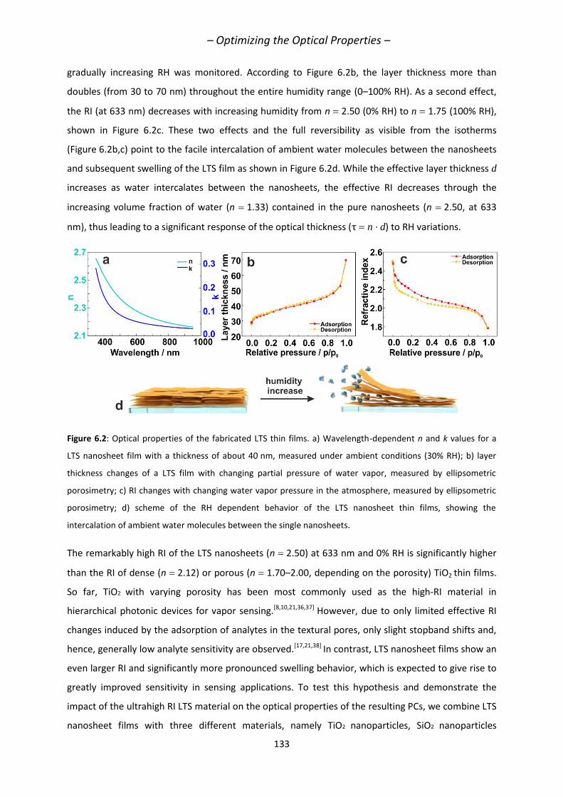
– Optimizing the Optical Properties –
133
gradually increasing RH was monitored. According to Figure 6.2b, the layer thickness more than
doubles (from 30 to 70 nm) throughout the entire humidity range (0–100% RH). As a second effect,
the RI (at 633 nm) decreases with increasing humidity from n 2.50 (0% RH) to n 1.75 (100% RH),
shown in Figure 6.2c. These two effects and the full reversibility as visible from the isotherms
(Figure 6.2b,c) point to the facile intercalation of ambient water molecules between the nanosheets
and subsequent swelling of the LTS film as shown in Figure 6.2d. While the effective layer thickness d
increases as water intercalates between the nanosheets, the effective RI decreases through the
increasing volume fraction of water (n 1.33) contained in the pure nanosheets (n 2.50, at 633
nm), thus leading to a significant response of the optical thickness (τn · d) to RH variations.
Figure 6.2: Optical properties of the fabricated LTS thin films. a) Wavelength-dependent n and k values for a
LTS nanosheet film with a thickness of about 40 nm, measured under ambient conditions (30% RH); b) layer
thickness changes of a LTS film with changing partial pressure of water vapor, measured by ellipsometric
porosimetry; c) RI changes with changing water vapor pressure in the atmosphere, measured by ellipsometric
porosimetry; d) scheme of the RH dependent behavior of the LTS nanosheet thin films, showing the
intercalation of ambient water molecules between the single nanosheets.
The remarkably high RI of the LTS nanosheets (n 2.50) at 633 nm and 0% RH is significantly higher
than the RI of dense (n 2.12) or porous (n 1.70–2.00, depending on the porosity) TiO2 thin films.
So far, TiO2 with varying porosity has been most commonly used as the high-RI material in
hierarchical photonic devices for vapor sensing.[8,10,21,36,37] However, due to only limited effective RI
changes induced by the adsorption of analytes in the textural pores, only slight stopband shifts and,
hence, generally low analyte sensitivity are observed.[17,21,38] In contrast, LTS nanosheet films show an
even larger RI and significantly more pronounced swelling behavior, which is expected to give rise to
greatly improved sensitivity in sensing applications. To test this hypothesis and demonstrate the
impact of the ultrahigh RI LTS material on the optical properties of the resulting PCs, we combine LTS
nanosheet films with three different materials, namely TiO2 nanoparticles, SiO2 nanoparticles
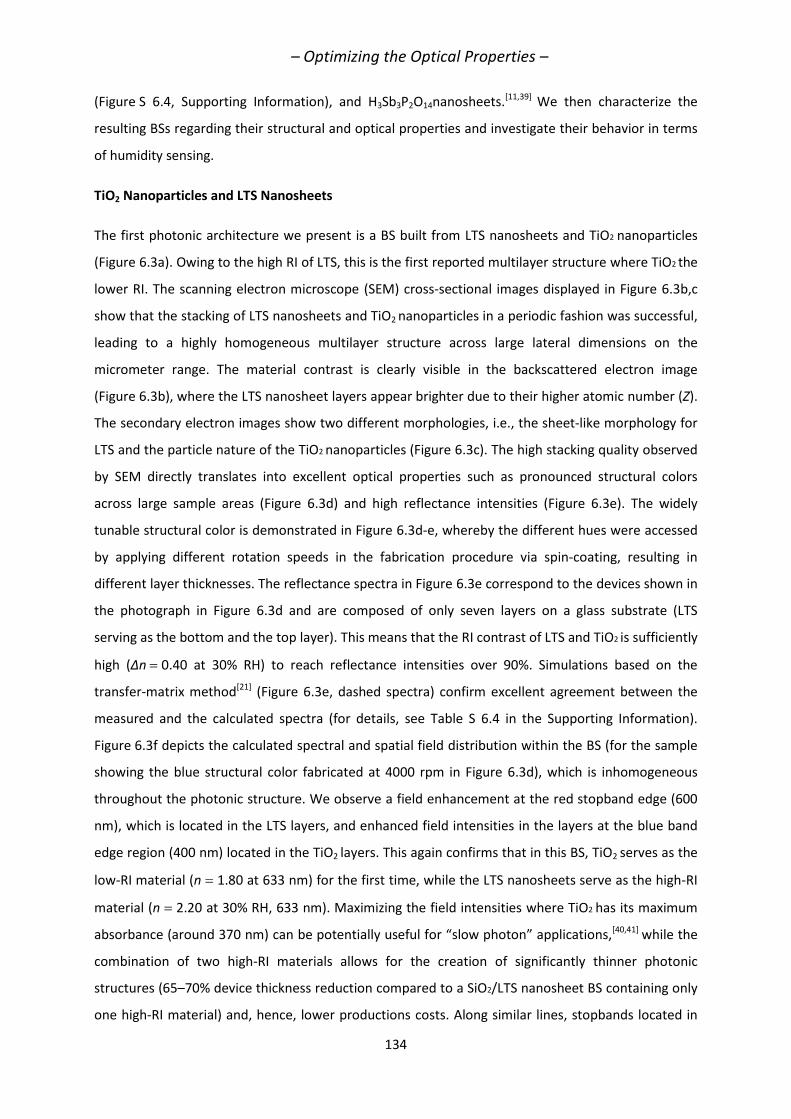
– Optimizing the Optical Properties –
134
(Figure S 6.4, Supporting Information), and H3Sb3P2O14nanosheets.[11,39] We then characterize the
resulting BSs regarding their structural and optical properties and investigate their behavior in terms
of humidity sensing.
TiO2 Nanoparticles and LTS Nanosheets
The first photonic architecture we present is a BS built from LTS nanosheets and TiO2 nanoparticles
(Figure 6.3a). Owing to the high RI of LTS, this is the first reported multilayer structure where TiO2 the
lower RI. The scanning electron microscope (SEM) cross-sectional images displayed in Figure 6.3b,c
show that the stacking of LTS nanosheets and TiO2 nanoparticles in a periodic fashion was successful,
leading to a highly homogeneous multilayer structure across large lateral dimensions on the
micrometer range. The material contrast is clearly visible in the backscattered electron image
(Figure 6.3b), where the LTS nanosheet layers appear brighter due to their higher atomic number (Z).
The secondary electron images show two different morphologies, i.e., the sheet-like morphology for
LTS and the particle nature of the TiO2 nanoparticles (Figure 6.3c). The high stacking quality observed
by SEM directly translates into excellent optical properties such as pronounced structural colors
across large sample areas (Figure 6.3d) and high reflectance intensities (Figure 6.3e). The widely
tunable structural color is demonstrated in Figure 6.3d-e, whereby the different hues were accessed
by applying different rotation speeds in the fabrication procedure via spin-coating, resulting in
different layer thicknesses. The reflectance spectra in Figure 6.3e correspond to the devices shown in
the photograph in Figure 6.3d and are composed of only seven layers on a glass substrate (LTS
serving as the bottom and the top layer). This means that the RI contrast of LTS and TiO2 is sufficiently
high (Δn 0.40 at 30% RH) to reach reflectance intensities over 90%. Simulations based on the
transfer-matrix method[21] (Figure 6.3e, dashed spectra) confirm excellent agreement between the
measured and the calculated spectra (for details, see Table S 6.4 in the Supporting Information).
Figure 6.3f depicts the calculated spectral and spatial field distribution within the BS (for the sample
showing the blue structural color fabricated at 4000 rpm in Figure 6.3d), which is inhomogeneous
throughout the photonic structure. We observe a field enhancement at the red stopband edge (600
nm), which is located in the LTS layers, and enhanced field intensities in the layers at the blue band
edge region (400 nm) located in the TiO2 layers. This again confirms that in this BS, TiO2 serves as the
low-RI material (n 1.80 at 633 nm) for the first time, while the LTS nanosheets serve as the high-RI
material (n 2.20 at 30% RH, 633 nm). Maximizing the field intensities where TiO2 has its maximum
absorbance (around 370 nm) can be potentially useful for “slow photon” applications,[40,41] while the
combination of two high-RI materials allows for the creation of significantly thinner photonic
structures (65–70% device thickness reduction compared to a SiO2/LTS nanosheet BS containing only
one high-RI material) and, hence, lower productions costs. Along similar lines, stopbands located in
– Optimizing the Optical Properties –
135
the IR range are more easily accessible, which may be useful, e.g., for applications in IR radiation
shielding.
Figure 6.3: Optical properties of the TiO2 nanoparticle / LTS nanosheet Bragg stacks. a) Scheme of the hybrid
nanoparticle / LTS nanosheet Bragg stack; b) back-scattered and c) secondary electron SEM cross section
images of the fabricated samples, showing the homogenous layered structure; d) photographs of three
samples consisting of seven layers on a glass substrate at ambient conditions, showing different structural
colors caused by different layer thicknesses (the samples were spin-coated at 3000 rpm, 4000 rpm and
5000 rpm rotation speed from left to right). The sample dimensions are 1.5x1.5 cm². e) Reflectance spectra
(solid lines) and simulated spectra (dashed lines, Table S 6.4) of the three samples fabricated at different
spin-coating speeds: 3000 rpm, 4000 rpm and 5000 rpm; f) spatial and spectral field distribution within the
sample fabricated at 4000 rpm rotation speed, whereby the structure is shown in reverse, i.e. the substrate is
located at 0.45 μm depth and the light source at 0 μm depth. The TiO2 layers are indicated with arrows.
SiO2 Nanoparticle and LTS Nanosheet Based Bragg Stacks
Motivated by the fact that LTS nanosheets are able to form high quality BSs with TiO2, we combined
this ultrahigh RI material with SiO2 nanoparticles (n 1.30, Figure 6.4a; Figure S 6.4, Supporting
Information), which is the most commonly used low-RI material in PC research. The secondary
electron and backscattered SEM images (Figure 6.4b,c) indicate homogeneous layering without
– Optimizing the Optical Properties –
136
intermixing and confirm the textural porosity of the nanoparticle layers, which provides accessibility
to analytes. The well-defined photonic stopbands of different five-layer systems on glass substrates,
along with their pronounced structural colors over a large area, viewed in reflectance, are shown in
Figure 6.4d,f. The photograph row in Figure 6.4e was taken in transmission mode. The good visibility
of the emblems below the glass substrate is a testament to the high transparency of the samples,
while the structural colors are still pronounced and complementary to the reflection colors shown in
Figure 6.4d. According to Figure 6.4f, the reflectance spectra of the fabricated samples
(Figure 6.4d,e) show high reflectance values of over 80% (for only five layers) and a bright Bragg peak
with a peak width of 350 nm. This hybrid multilayer system has the highest RI contrast (Δn 0.90 at
30% RH, 633 nm) that was reported in any BS to date (Figure 6.4a). The RI contrast value is even
higher at lower RH values (Δn 1.20 at 0% RH, 633 nm), as the RI of the LTS nanosheets strongly
depends on the ambient water amount. So far, the highest RI contrasts found in BSs in the literature
reach maximum values of Δn 0.83,[17] Δn 0.84,[19]
and Δn 0.89,[18] well below the RI contrast of
our system. Comparing the experimental reflectance spectra with the simulated spectra (Figure 6.4f
dashed lines, Table S 6.5, Supporting Information) shows good agreement and confirms that the
broad stopband arises from the superior RI contrast,[1] rather than from defects or other
inhomogeneities. Increasing the number of layers above five resulted in more defects and more
pronounced scattering, which is indicated by the higher reflectance minima (Figure S 6.5, Supporting
Information). Hence, for further studies, we use samples with five layers, as they already have a
sufficiently high optical quality.
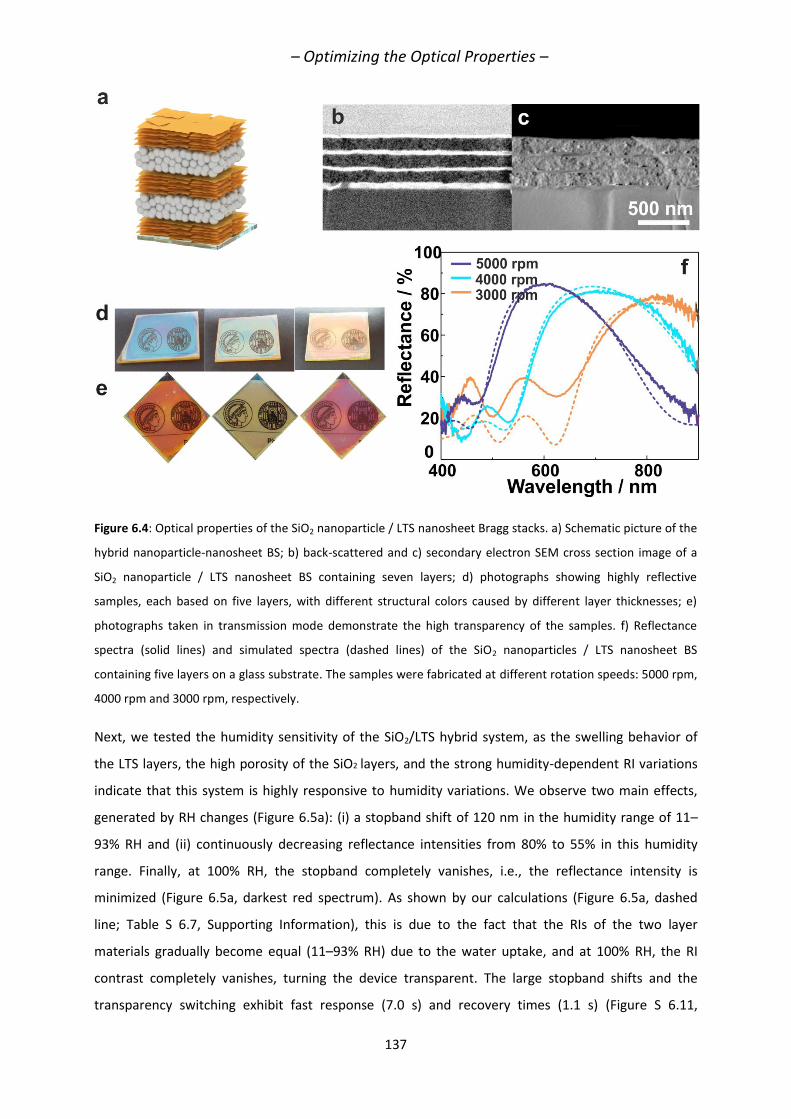
– Optimizing the Optical Properties –
137
Figure 6.4: Optical properties of the SiO2 nanoparticle / LTS nanosheet Bragg stacks. a) Schematic picture of the
hybrid nanoparticle-nanosheet BS; b) back-scattered and c) secondary electron SEM cross section image of a
SiO2 nanoparticle / LTS nanosheet BS containing seven layers; d) photographs showing highly reflective
samples, each based on five layers, with different structural colors caused by different layer thicknesses; e)
photographs taken in transmission mode demonstrate the high transparency of the samples. f) Reflectance
spectra (solid lines) and simulated spectra (dashed lines) of the SiO2 nanoparticles / LTS nanosheet BS
containing five layers on a glass substrate. The samples were fabricated at different rotation speeds: 5000 rpm,
4000 rpm and 3000 rpm, respectively.
Next, we tested the humidity sensitivity of the SiO2/LTS hybrid system, as the swelling behavior of
the LTS layers, the high porosity of the SiO2 layers, and the strong humidity-dependent RI variations
indicate that this system is highly responsive to humidity variations. We observe two main effects,
generated by RH changes (Figure 6.5a): (i) a stopband shift of 120 nm in the humidity range of 11–
93% RH and (ii) continuously decreasing reflectance intensities from 80% to 55% in this humidity
range. Finally, at 100% RH, the stopband completely vanishes, i.e., the reflectance intensity is
minimized (Figure 6.5a, darkest red spectrum). As shown by our calculations (Figure 6.5a, dashed
line; Table S 6.7, Supporting Information), this is due to the fact that the RIs of the two layer
materials gradually become equal (11–93% RH) due to the water uptake, and at 100% RH, the RI
contrast completely vanishes, turning the device transparent. The large stopband shifts and the
transparency switching exhibit fast response (7.0 s) and recovery times (1.1 s) (Figure S 6.11,
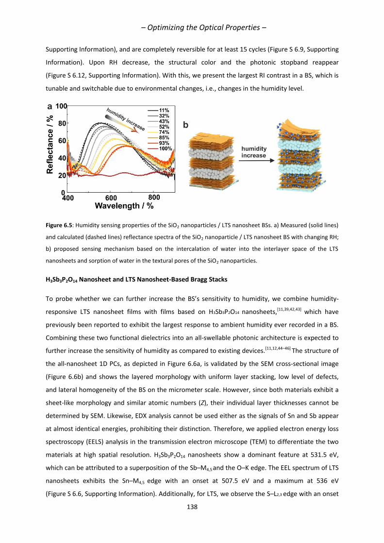
– Optimizing the Optical Properties –
138
Supporting Information), and are completely reversible for at least 15 cycles (Figure S 6.9, Supporting
Information). Upon RH decrease, the structural color and the photonic stopband reappear
(Figure S 6.12, Supporting Information). With this, we present the largest RI contrast in a BS, which is
tunable and switchable due to environmental changes, i.e., changes in the humidity level.
Figure 6.5: Humidity sensing properties of the SiO2 nanoparticles / LTS nanosheet BSs. a) Measured (solid lines)
and calculated (dashed lines) reflectance spectra of the SiO2 nanoparticle / LTS nanosheet BS with changing RH;
b) proposed sensing mechanism based on the intercalation of water into the interlayer space of the LTS
nanosheets and sorption of water in the textural pores of the SiO2 nanoparticles.
H3Sb3P2O14 Nanosheet and LTS Nanosheet-Based Bragg Stacks
To probe whether we can further increase the BS’s sensitivity to humidity, we combine humidity-
responsive LTS nanosheet films with films based on H3Sb3P2O14 nanosheets,[11,39,42,43] which have
previously been reported to exhibit the largest response to ambient humidity ever recorded in a BS.
Combining these two functional dielectrics into an all-swellable photonic architecture is expected to
further increase the sensitivity of humidity as compared to existing devices.[11,12,44–46] The structure of
the all-nanosheet 1D PCs, as depicted in Figure 6.6a, is validated by the SEM cross-sectional image
(Figure 6.6b) and shows the layered morphology with uniform layer stacking, low level of defects,
and lateral homogeneity of the BS on the micrometer scale. However, since both materials exhibit a
sheet-like morphology and similar atomic numbers (Z), their individual layer thicknesses cannot be
determined by SEM. Likewise, EDX analysis cannot be used either as the signals of Sn and Sb appear
at almost identical energies, prohibiting their distinction. Therefore, we applied electron energy loss
spectroscopy (EELS) analysis in the transmission electron microscope (TEM) to differentiate the two
materials at high spatial resolution. H3Sb3P2O14 nanosheets show a dominant feature at 531.5 eV,
which can be attributed to a superposition of the Sb–M4,5 and the O–K edge. The EEL spectrum of LTS
nanosheets exhibits the Sn–M4,5 edge with an onset at 507.5 eV and a maximum at 536 eV
(Figure S 6.6, Supporting Information). Additionally, for LTS, we observe the S–L2,3 edge with an onset
– Optimizing the Optical Properties –
139
at 166 eV. For both materials, an additional feature is visible at 686.5 eV in the spectra. This minor
feature cannot be identified unequivocally and most likely originates from a contamination
introduced by the focused ion beam (FIB) sample preparation. To extract the spatial distribution of
the nanosheets across the BS (TEM cross–sectional image shown in Figure 6.6c), the local EELS edge
intensities were determined, and the resulting elemental distribution maps are depicted in
Figure 6.6d–g. For experimental details, see the experimental section and Figures S 6.6 and S 6.7 in
the Supporting Information. The EELS maps (Figure 6.6d,e) clearly confirm the layered morphology
composed of alternating H3Sb3P2O14 and LTS layers with thicknesses of 50 ±8 and 41 ±8 nm,
respectively. This alternating arrangement of the two different nanosheet materials is also confirmed
by the mapping of the S–L2,3 edge (Figure S 6.7, Supporting Information), and is only found in the LTS
nanosheet layer, yielding a thickness of 49 nm, which corresponds well to the layer thicknesses
determined from the Sn edges. Additionally, the layer thicknesses were also confirmed by
spectroscopic ellipsometry measurements at ambient conditions (Figure S 6.8 and Table S 6.3,
Supporting Information). Hereby, the experimental data were fitted with a periodic model including
three double layers on a silicon substrate. The layer thicknesses and the RIs were fitted to d 44 nm
and n 2.50 (at 633 nm) for LTS and d 62 nm and n 1.56 (at 633 nm) for H3Sb3P2O14 at ambient
RH, which is in excellent agreement with the EELS element mapping data. According to Figure 6.6h,
the homogeneously stacked layered structure is also confirmed by the high reflectance intensities of
the Bragg peak, created by the alternating arrangement of seven layers of LTS and H3Sb3P2O14
nanosheets on a glass substrate, terminated by a top layer of LTS nanosheets. By changing the spin-
coating speeds and the layer thicknesses within the stack, different structural colors are accessible all
over the visible spectral range (Figure 6.6h,i). Simulations of the reflectance spectra (Figure 6.6h,
dashed lines; Table S 6.6, Supporting Information) based on the RIs extracted by ellipsometric
porosimetry confirm the layer thicknesses determined by the EELS mapping. As shown in Figure 6.6h,
seven alternating layers of the two nanosheet materials with an RI contrast of Δn 0.65 are
sufficient to obtain reflectance intensities of 90%. This allows for the fabrication of ultrathin photonic
structures with good optical quality, as only a few layers are needed to reach high reflectance values.
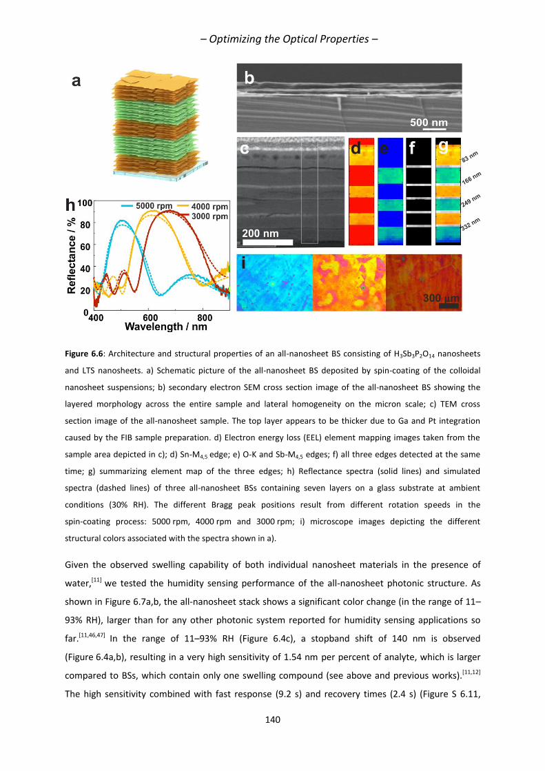
– Optimizing the Optical Properties –
140
Figure 6.6: Architecture and structural properties of an all-nanosheet BS consisting of H3Sb3P2O14 nanosheets
and LTS nanosheets. a) Schematic picture of the all-nanosheet BS deposited by spin-coating of the colloidal
nanosheet suspensions; b) secondary electron SEM cross section image of the all-nanosheet BS showing the
layered morphology across the entire sample and lateral homogeneity on the micron scale; c) TEM cross
section image of the all-nanosheet sample. The top layer appears to be thicker due to Ga and Pt integration
caused by the FIB sample preparation. d) Electron energy loss (EEL) element mapping images taken from the
sample area depicted in c); d) Sn-M4,5 edge; e) O-K and Sb-M4,5 edges; f) all three edges detected at the same
time; g) summarizing element map of the three edges; h) Reflectance spectra (solid lines) and simulated
spectra (dashed lines) of three all-nanosheet BSs containing seven layers on a glass substrate at ambient
conditions (30% RH). The different Bragg peak positions result from different rotation speeds in the
spin-coating process: 5000 rpm, 4000 rpm and 3000 rpm; i) microscope images depicting the different
structural colors associated with the spectra shown in a).
Given the observed swelling capability of both individual nanosheet materials in the presence of
water,[11] we tested the humidity sensing performance of the all-nanosheet photonic structure. As
shown in Figure 6.7a,b, the all-nanosheet stack shows a significant color change (in the range of 11–
93% RH), larger than for any other photonic system reported for humidity sensing applications so
far.[11,46,47] In the range of 11–93% RH (Figure 6.4c), a stopband shift of 140 nm is observed
(Figure 6.4a,b), resulting in a very high sensitivity of 1.54 nm per percent of analyte, which is larger
compared to BSs, which contain only one swelling compound (see above and previous works).[11,12]
The high sensitivity combined with fast response (9.2 s) and recovery times (2.4 s) (Figure S 6.11,
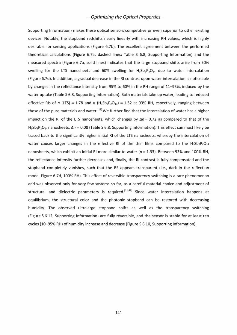
– Optimizing the Optical Properties –
141
Supporting Information) makes these optical sensors competitive or even superior to other existing
devices. Notably, the stopband redshifts nearly linearly with increasing RH values, which is highly
desirable for sensing applications (Figure 6.7b). The excellent agreement between the performed
theoretical calculations (Figure 6.7a, dashed lines; Table S 6.8, Supporting Information) and the
measured spectra (Figure 6.7a, solid lines) indicates that the large stopband shifts arise from 50%
swelling for the LTS nanosheets and 60% swelling for H3Sb3P2O14 due to water intercalation
(Figure 6.7d). In addition, a gradual decrease in the RI contrast upon water intercalation is noticeable
by changes in the reflectance intensity from 95% to 60% in the RH range of 11–93%, induced by the
water uptake (Table S 6.8, Supporting Information). Both materials take up water, leading to reduced
effective RIs of n (LTS) 1.78 and n (H3Sb3P2O14) 1.52 at 93% RH, espectively, ranging between
those of the pure materials and water.[11] We further find that the intercalation of water has a higher
impact on the RI of the LTS nanosheets, which changes by Δn 0.72 as compared to that of the
H3Sb3P2O14 nanosheets, Δn 0.08 (Table S 6.8, Supporting Information). This effect can most likely be
traced back to the significantly higher initial RI of the LTS nanosheets, whereby the intercalation of
water causes larger changes in the effective RI of the thin films compared to the H3Sb3P2O14
nanosheets, which exhibit an initial RI more similar to water (n 1.33). Between 93% and 100% RH,
the reflectance intensity further decreases and, finally, the RI contrast is fully compensated and the
stopband completely vanishes, such that the BS appears transparent (i.e., dark in the reflection
mode, Figure 6.7d, 100% RH). This effect of reversible transparency switching is a rare phenomenon
and was observed only for very few systems so far, as a careful material choice and adjustment of
structural and dielectric parameters is required.[11,48] Since water intercalation happens at
equilibrium, the structural color and the photonic stopband can be restored with decreasing
humidity. The observed ultralarge stopband shifts as well as the transparency switching
(Figure S 6.12, Supporting Information) are fully reversible, and the sensor is stable for at least ten
cycles (10–95% RH) of humidity increase and decrease (Figure S 6.10, Supporting Information).
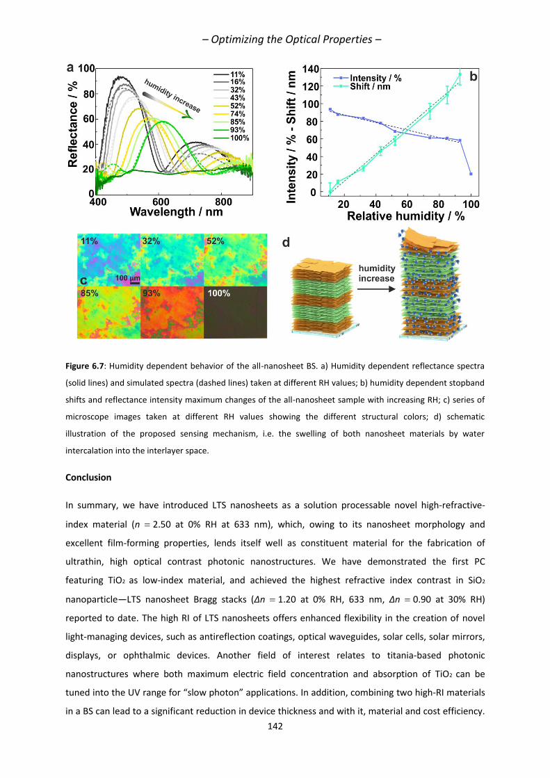
– Optimizing the Optical Properties –
142
Figure 6.7: Humidity dependent behavior of the all-nanosheet BS. a) Humidity dependent reflectance spectra
(solid lines) and simulated spectra (dashed lines) taken at different RH values; b) humidity dependent stopband
shifts and reflectance intensity maximum changes of the all-nanosheet sample with increasing RH; c) series of
microscope images taken at different RH values showing the different structural colors; d) schematic
illustration of the proposed sensing mechanism, i.e. the swelling of both nanosheet materials by water
intercalation into the interlayer space.
Conclusion
In summary, we have introduced LTS nanosheets as a solution processable novel high-refractive-
index material (n 2.50 at 0% RH at 633 nm), which, owing to its nanosheet morphology and
excellent film-forming properties, lends itself well as constituent material for the fabrication of
ultrathin, high optical contrast photonic nanostructures. We have demonstrated the first PC
featuring TiO2 as low-index material, and achieved the highest refractive index contrast in SiO2
nanoparticle—LTS nanosheet Bragg stacks (Δn 1.20 at 0% RH, 633 nm, Δn 0.90 at 30% RH)
reported to date. The high RI of LTS nanosheets offers enhanced flexibility in the creation of novel
light-managing devices, such as antireflection coatings, optical waveguides, solar cells, solar mirrors,
displays, or ophthalmic devices. Another field of interest relates to titania-based photonic
nanostructures where both maximum electric field concentration and absorption of TiO2 can be
tuned into the UV range for “slow photon” applications. In addition, combining two high-RI materials
in a BS can lead to a significant reduction in device thickness and with it, material and cost efficiency.
– Optimizing the Optical Properties –
143
This effect could be exploited, for example, for devices used in radiation shielding, with a photonic
stopband placed in the IR spectral range. We have further demonstrated the first allnanosheet Bragg
stacks composed of LTS and antimony phosphate, H3Sb3P2O14, nanosheets, which are both able to
take up significant amounts of water into their interlayer space. Upon exposure to ambient humidity,
we observe a full-spectral, linear stopband shift with increasing relative humidity between 11% and
93% RH, which is fully reversible. Notably, due to the high RI contrast, we achieve reflectance
intensities above 90% (at 10% RH) for a device consisting of only seven layers (1 m) in total. This
novel BS architecture, therefore, presents an ultrasensitive colorimetric humidity sensor entirely
based on functional 2D materials, which, more generally, constitutes a generic material platform for
the detection of a variety of analytes.
6.6 EXPERIMENTAL SECTION
Material synthesis
Bulk Li2Sn2S5 was synthesized via a one-step solid state synthesis.[32] The precursors, Li2S, Sn and S
were stoichiometrically mixed under inert gas atmosphere, filled into a glassy carbon crucible and
vacuum-sealed in a quartz tube. A slight excess of sulfur (3wt%) was applied in order to ensure the
complete oxidation of Sn. The tubes were heated to 750 °C with a ramp of 1 °C min-1 for 48 h and
subsequently quenched to room temperature.
K3Sb3P2O14 was also synthesized by a solid state reaction as described elsewhere.[11] For protonation,
4 g of the resulting white powder was stirred in 250 ml of 8 M HNO3 overnight and washed with pure
water. To ensure complete protonation, this step was repeated once again.
Preparation of colloidal suspensions
For exfoliation, the bulk Li2Sn2S5 was shaken in water for several hours with a concentration of 1 g L-1.
To ensure complete exfoliation, the suspension was sonicated for 60 min. To collect the exfoliated
nanosheets, the suspension was centrifuged at 24000 rpm for 30 min. The brownish pellet was
resuspended in a water-ethanol mixture (60vol% ethanol) with a concentration of 60 mg mL-1.
Afterwards, the suspension was sonicated for 2 h before using it in the BS fabrication.
The bulk H3Sb3P2O14 was exfoliated likewise by stirring the protonated compound in pure water
overnight. The suspension was centrifuged first at 3000 rpm to get rid of the non-exfoliated residual
bulk and then at 18000 rpm to obtain the nanosheets. The gel-like pellet was dried at 100 °C and re-
suspended in a water-ethanol mixture (60 vol% ethanol) with a concentration of 27.5 mg mL-1. This
suspension was sonicated 2 h before spin-coating.
– Optimizing the Optical Properties –
144
TiO2 was synthesized by hydrolysis of Ti(OEt)4 in diluted acid.[9] 12.5 mL TEOT
(Tetraethylorthotitanate, Sigma Aldrich) was added dropwise under vigorous stirring to 75 mL of
0.1 M HNO3 and heated at 80 °C for 8 h. The white suspension was sonicated for 3 h and washed
three times by centrifuging the particles at 24000 rpm and redispersing the pellet in methanol. A final
concentration of 3wt% was used for spin-coating.
Colloidal SiO2 (LUDOX, SigmaAldrich) was diluted with methanol to 3.2wt% and after 10 min
sonication directly used for spin-coating.
Bragg stack preparation
All BSs were prepared by spin-coating (WS-650S-NPP-Lite, Laurell Technologies Corporation) using
the stable colloidal suspensions with the concentrations given above. To access different film
thicknesses and, hence, structural colors, different spin-coating speeds and the number of deposition
steps were varied. 150 μL of the colloidal suspensions were spin-coated alternatingly on plasma-
cleaned glass substrates (1.5 cm x 1.5 cm) for 1 min with defined speeds (3000 rpm, 4000 rpm and
5000 rpm) and with an acceleration of 7000 rpm s-1. The first layer on top of the glass substrate and
also the last one were the LTS nanosheets, to achieve the highest achievable RI contrast at the
interfaces. To create one layer within the Bragg stack, LTS was deposited for all samples in two steps
and the samples were heated after each deposition step to 80 °C for 15 min in order to stabilize the
layers and to get rid of the residual solvents.
Characterization
SEM images of the LTS bulk material and the EDX analysis to verify the S:Sn ratio was performed on a
FEI Helios G3 UC scanning electron microscope (SEM). In addition, inductively coupled plasma (ICP)
measurements were performed on a Varian Vista RL. X-ray diffraction (XRD) patterns were recorded
on a powder X-ray diffractometer (Stadi P, STOE) working with Ge(111) monochromated Mo-K1
radiation (λ = 70.926 pm) and a Mythen 1K Detector (Dektris). The crystalline nanosheet compounds
were identified by comparing them the powder diffraction patterns of the bulk materials.[32, 49]
Cross-section images of the BSs were taken with a Zeiss Gemini Ultra Field Emission SEM. For the
TEM measurement, the sample was cut via focused ion beam (FIB, Zeiss 1540EsB) with a 30 kV Ga ion
beam and the surface was polished with a 3 kV beam. The TEM cross section measurement was
performed on a FEI Titan Themis microscope 60-300 kV equipped with a Cs corrector for the probe.
EELS investigations were performed in scanning transmission mode with a convergence semi-angle of
16.6 mrad and an energy resolution of 0.75 eV. To reduce the effect of the electron irradiation on the
material, sub-pixel scanning was applied during the spectrum image acquisition. The EELS maps for
the spectral region of 100 to 612.25 eV were generated by integrating the intensity of background
– Optimizing the Optical Properties –
145
corrected spectra in defined energy windows. The background was subtracted by performing a
power law fit for an energy width of 60 eV starting from 429 eV for the Sn-M4,5 edge and from 467 eV
for the Sb-M4,5/O-K edge. Subsequently, the intensity of the edges was integrated in an energy
window of 100 eV starting at 507.5 eV for the Sn-M4,5 and at 530.5 eV for the Sb-M4,5/O-K edge. The
same procedure was used to generate the intensity map of the S-L2,3 edge, but in that case the
background was corrected by a power law fit in the spectral range of 130.25 to 160.25 eV and the
intensity was integrated between 161 and 216 eV.
Ellipsometric porosimetry measurements on the thin films were carried out by the porosimetry tool
of a Sopra PS-1000 ellipsometer, whereby the samples were equilibrated at selected partial pressure
values of water vapor for 15 min. The measured spectra were fitted with the software Sopra SAE
using the model combination Cauchy and Lorentz. For the nanosheet thin films, both the layer
thickness and the RI were fitted over the relative pressure range simultaneously.
Microscope images were taken from the BS surface with an optical microscope (DM2500, Leica) and
simultaneously reflectance spectra were measured at normal incidence with a fiber optic
spectrometer (USB2000+, Ocean Optics) attached to the microscope.
To monitor the optical changes with changes in RH, the BSs were kept in a closed stainless steel
chamber with a total volume of 5 mL and with a transparent glass window. In the chamber, 0.7 mL of
saturated salt solutions were filled without touching the sample surface, and kept at 25 °C to define
the humidity in the closed atmosphere.[50-51] At each step, 20 min equilibration time was needed.
Dynamic cycling measurements between 10-95% RH were performed using a nitrogen flow setup.
Simulations
Numerical calculations of the reflectance spectra were carried out using a Matlab code based on a
full-vector calculation using the transfer matrix method as reported elsewhere.[21] The layer
thicknesses at 0% RH were taken from the SEM cross section images. The (wavelength dependent)
RIs were taken from the porosimetry measurements.
6.7 ACKNOWLEDGEMENTS
Financial support was granted by the Max Planck Society, the University of Munich (LMU), the Center
for NanoScience (CeNS), and the Deutsche Forschungsgemeinschaft (DFG) through the Cluster of
Excellence Nanosystems Initiative Munich (NIM). The authors thank Viola Duppel and Christian Minke
for SEM and EDX measurements, Bernhard Fenk for the preparation of the TEM-EELS sample by FIB,
– Optimizing the Optical Properties –
146
Jakob Blahusch for help with the experimental work and Jaroslava Obel for the ICP measurements.
We thank to Anna-Katharina Hatz for scientific discussions.
6.8 REFERENCES
[1] J. D. Joannopoulos, S. G. Johnson, J. N. Winn, R. D. Meade, Photonic crystals: molding the flow of
light, Princeton university press, 2011.
[2] J. D. Joannopoulos, P. R. Villeneuve, S. Fan, Nature 1997, 386, 143-149.
[3] L. D. Bonifacio, B. V. Lotsch, D. P. Puzzo, F. Scotognella, G. A. Ozin, Adv. Mater. 2009, 21, 1641-
1646.
[4] S. Colodrero, M. Ocaña, H. Míguez, Langmuir 2008, 24, 4430-4434.
[5] S. Colodrero, M. Ocana, A. R. Gonzalez-Elipe, H. Miguez, Langmuir 2008, 24, 9135-9139.
[6] B. V. Lotsch, G. A. Ozin, ACS Nano, 2008, 2, 2065-2074.
[7] S. Y. Choi, M. Mamak, G. von Freymann, N. Chopra, G. A. Ozin, Nano Lett. 2006, 6, 2456-2461.
[8] A. Ranft, F. Niekiel, I. Pavlichenko, N. Stock, B. V. Lotsch, Chem. Mater. 2015, 27, 1961–1970.
[9] F. M. Hinterholzinger, A. Ranft, J. M. Feckl, B. Ruhle, T. Bein, B. V. Lotsch, J. Mater. Chem. 2012,
22, 10356-10362.
[10] I. Pavlichenko, E. Broda, Y. Fukuda, K. Szendrei, A. K. Hatz, G. Scarpa, P. Lugli, C. Brauchle, B. V.
Lotsch, Mater. Horiz. 2015, 2, 299-308.
[11] K. Szendrei, P. Ganter, O. Sànchez-Sobrado, R. Eger, A. Kuhn, B. V. Lotsch, Adv. Mater. 2015, 27,
6341-6348.
[12] P. Ganter, K. Szendrei, B. V. Lotsch, Adv. Mater. 2016, 28, 7294-7294.
[13] M. Anaya, J. P. Correa-Baena, G. Lozano, M. Saliba, P. Anguita, B. Roose, A. Abate, U. Steiner, M.
Gratzel, M. E. Calvo, A. Hagfeldt, H. Miguez, J. Mater. Chem. A 2016, 4, 11214-11221.
[14] J. J. Steele, A. C. van Popta, M. M. Hawkeye, J. C. Sit, M. J. Brett, Sens. Actuators, B 2006, 120,
213-219.
[15] M. M. Hawkeye, M. J. Brett, Adv. Func. Mater. 2011, 21, 3652-3658.
[16] N. Hidalgo, M. E. Calvo, H. Míguez, Small 2009, 5, 2309-2315.
[17] M. Anaya, A. Rubino, M. E. Calvo, H. Miguez, J. Mater. Chem. C 2016, 4, 4532-4537.
[18] W. J. Nimens, L. Whittaker-Brooks, M. H. Bartl, J. Mater. Chem. C 2016, 4, 668-672.
[19] B. Brudieu, A. L. Bris, J. Teisseire, F. Guillemot, G. Dantelle, S. Misra, P. R. i. Cabarrocas, F. Sorin,
T. Gacoin, Adv. Opt. Mater. 2014, 2, 1105-1112.
[20] J. L. H. Chau, Y.-M. Lin, A.-K. Li, W.-F. Su, K.-S. Chang, S. L.-C. Hsu, T.-L. Li, Mater. Lett. 2007, 61,
2908-2910.
[21] M. C. Fuertes, S. Colodrero, G. Lozano, A. R. González-Elipe, D. Grosso, C. Boissière, C. Sánchez,
G. J. d. A. A. Soler-Illia, H. Míguez, J. Phys. Chem. C 2008, 112, 3157-3163.
– Optimizing the Optical Properties –
147
[22] E. Redel, C. Huai, M. Renner, G. von Freymann, G. A. Ozin, Small 2011, 7, 3465-3471.
[23] M. E. Calvo, J. R. Castro Smirnov, H. Míguez, J. Polym. Sci., Part B: Polym. Phys. 2012, 50,
945-956.
[24] J. R. C. Smirnov, M. Ito, M. E. Calvo, C. López-López, A. Jiménez-Solano, J. F. Galisteo-López, P.
Zavala-Rivera, K. Tanaka, E. Sivaniah, H. Míguez, Adv. Opt. Mater. 2015, 3, 1633-1639.
[25] B. Gospodinov, J. Dikova, S. Mintova, T. Babeva, J. Phys.: Conf. Ser. 2012, 398, 012026.
[26] S. Gürakar, T. Serin, N. Serin, Appl. Surf. Sci. 2015, 352, 16-22.
[27] A. Jiménez-Solano, M. Anaya, M. E. Calvo, M. Alcon-Camas, C. Alcañiz, E. Guillén, N. Martínez, M.
Gallas, T. Preussner, R. Escobar-Galindo, H. Míguez, Adv. Opt. Mater. 2017, 5 , 1600833.
[28] C. Bariáin, I. R. Ma as, F. J. Arregui, M. López-Amo, Sens. Actuators, B 2000, 69, 127-131.
[29] B. V. Lotsch, G. A. Ozin, Adv. Mater. 2008, 20, 4079-4084.
[30] Z. Wang, J. Zhang, J. Xie, C. Li, Y. Li, S. Liang, Z. Tian, T. Wang, H. Zhang, H. Li, W. Xu, B. Yang, Adv.
Funct. Mater. 2010, 20, 3784-3790.
[31] B. V. Lotsch, G. A. Ozin, J. Am. Chem. Soc. 2008, 130, 15252-15253.
[32] A. Kuhn, T. Holzmann, J. Nuss, B. V. Lotsch, J. Mater. Chem. A 2014, 2, 6100-6106.
[33] T. Holzmann, L. M. Schoop, M. N. Ali, I. Moudrakovski, G. Gregori, J. Maier, R. J. Cava, B. V.
Lotsch, Energy Environ. Sci. 2016, 9, 2578-2585.
[34] H. S. Jung, P. Verwilst, W. Y. Kim, J. S. Kim, Chem. Soc. Rev. 2016, 45, 1242-1256.
[35] S. Sikarwar, B. C. Yadav, Sens. Actuators A 2015, 233, 54-70.
[36] G. von Freymann, V. Kitaev, B. V. Lotsch, G. A. Ozin, Chem. Soc. Rev. 2013, 42, 2528-2554.
[37] A. T. Exner, I. Pavlichenko, B. V. Lotsch, G. Scarpa, P. Lugli, ACS Appl. Mater. Interfaces 2013, 5,
1575-1582.
[38] A. Ranft, I. Pavlichenko, K. Szendrei, P. M. Zehetmaier, Y. Hu, A. von Mankowski, B. V. Lotsch,
Microporous Mesoporous Mater. 2015, 216, 216-224.
[39] Y. Piffard, A. Verbaere, A. Lachgar, S. Deniard-Courant, M. Tournoux, Rev. Chim. Miner. 1986, 23,
766-775.
[40] J. I. L. Chen, G. von Freymann, S. Y. Choi, V. Kitaev, G. A. Ozin, Adv. Mater. 2006, 18, 1915-1919.
[41] T. Baba, Nat. Photon 2008, 2, 465-473.
[42] J.-C. P. Gabriel, F. Camerel, B. J. Lemalre, H. Desvaux, P. Davidson, P. Batail, Nature 2001, 413,
504-508.
[43] S. Deniard-Courant, Y. Piffard, P. Barboux, J. Livage, Solid State Ionics 1988, 27, 189-194.
[44] C.-Y. Lee, G.-B. Lee, Sens. Lett. 2005, 3, 1-15.
[45] R. A. Barry, P. Wiltzius, Langmuir 2005, 22, 1369-1374.
[46] E. Tian, J. Wang, Y. Zheng, Y. Song, L. Jiang, D. Zhu, J. Mater. Chem. 2008, 18, 1116-1122.
[47] R. Xuan, Q. Wu, Y. Yin, J. Ge, J. Mater. Chem. 2011, 21, 3672-3676.

– Optimizing the Optical Properties –
148
[48] M. N. Ghazzal, O. Deparis, J. De Coninck, E. M. Gaigneaux, J. Mater. Chem. C 2013, 1, 6202-6209.
[49] Y. Piffard, A. Lachgar, M. Tournoux, J. Solid State Chem. 1985, 58, 253-256.
[50] P. W. Winston, D. H. Bates, Ecology 1960, 41, 232-237.
[51] L. Greenspan, J. Res. Nat. Bur. Stand. 1977, 81A, 89-96.
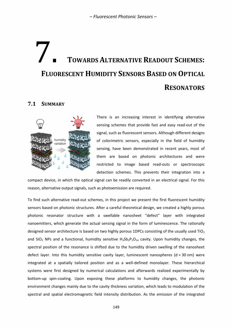
– Fluorescent Photonic Sensors –
149
7. TOWARDS ALTERNATIVE READOUT SCHEMES:
FLUORESCENT HUMIDITY SENSORS BASED ON OPTICAL
RESONATORS
7.1 SUMMARY
There is an increasing interest in identifying alternative
sensing schemes that provide fast and easy read-out of the
signal, such as fluorescent sensors. Although different designs
of colorimetric sensors, especially in the field of humidity
sensing, have been demonstrated in recent years, most of
them are based on photonic architectures and were
restricted to image based read-outs or spectroscopic
detection schemes. This prevents their integration into a
compact device, in which the optical signal can be readily converted in an electrical signal. For this
reason, alternative output signals, such as photoemission are required.
To find such alternative read-out schemes, in this project we present the first fluorescent humidity
sensors based on photonic structures. After a careful theoretical design, we created a highly porous
photonic resonator structure with a swellable nanosheet “defect” layer with integrated
nanoemitters, which generate the actual sensing signal in the form of luminescence. The rationally
designed sensor architecture is based on two highly porous 1DPCs consisting of the usually used TiO2
and SiO2 NPs and a functional, humidity sensitive H3Sb3P2O14 cavity. Upon humidity changes, the
spectral position of the resonance is shifted due to the humidity driven swelling of the nanosheet
defect layer. Into this humidity sensitive cavity layer, luminescent nanospheres (d = 30 nm) were
integrated at a spatially tailored position and as a well-defined monolayer. These hierarchical
systems were first designed by numerical calculations and afterwards realized experimentally by
bottom-up spin-coating. Upon exposing these platforms to humidity changes, the photonic
environment changes mainly due to the cavity thickness variation, which leads to modulation of the
spectral and spatial electromagnetic field intensity distribution. As the emission of the integrated
– Fluorescent Photonic Sensors –
150
dyes couples to the photonic modes sustained by the multilayered structure, changes in the
distribution of these modes cause variations in the photoluminescence. In extreme cases, this results
in the complete suppression of the emission; in other words, we could turn on and off the emission
by humidity variations. The interplay between the luminescent properties of an emitter and its
photonic environment is a central concept in our approach and implies a fundamental advantage, as
the emitters are not chemically altered during the detection process. We also showed evidence of
their versatility, in terms of structural design, to provide a tailored response to specific levels of
humidity. Guided by theoretical optical design of the resonator architecture and subsequent
experimental realization, we presented two embodiments of fluorescent photonic humidity sensors
featuring turn-on and turn-off detection schemes.
This project was carried out in an on-site cooperation with the Multifunctional Optical Materials
Group at the ICMSE-CSIC, Sevilla Spain. Katalin Szendrei fabricated the photonic resonator structures,
performed the optical measurements, planned the project, edited the figures and wrote the
manuscript. Alberto Jiménez-Solano performed the theoretical calculations in order to optimize the
structures and understand the sensing mechanism, assisted with the optical measurements, edited
the figures and wrote the manuscript. Gabriel Lozano assisted with the optical measurements and
wrote the manuscript. Hernán Míguez discussed the results and wrote the manuscript.
– Fluorescent Photonic Sensors –
151
7.2 FLUORESCENT HUMIDITY SENSORS BASED ON PHOTONIC
RESONATORS
Katalin Szendrei,* Alberto Jiménez-Solano,* Gabriel Lozano, Bettina V. Lotsch, Hernán Míguez
* These authors contributed equally to this work.
Published in Advanced Optical Materials, 2017, 5, 1700663.
DOI: 10.1002/adom.201700663
http://onlinelibrary.wiley.com/doi/10.1002/adom.201700663/full
7.3 ABSTRACT
Among the different approaches to humidity sensing available, those based on fluorescent signals
are gathering a great deal of attention due to their fast response and versatility of detection and
design. So far, all proposals have focused on the use of luminescent probes whose emission is either
triggered or inhibited by the presence of water that reacts or alters their chemical environment,
hence inducing the signal change. Here, a novel concept in fluorescent humidity sensing based on
combining stimuli-responsive photonic resonators with molecular fluorescent probes is introduced.
The resonator is assembled from humidity-swellable antimony phosphate nanosheets embedding a
planar light-emitting probe, whose emission is dramatically modified by the changes that ambient
humidity causes in its photonic environment. Guided by “in silico” optical design of the resonator
architecture and subsequent experimental realization, two embodiments of fluorescent photonic
humidity sensors featuring turn-on and turn-off detection schemes are presented. The interplay
between the luminescent properties of an emitter and its photonic environment implies a
fundamental advantage as the emitters are not chemically altered during the detection process. At
the same time, it paves the way toward a new generation of photonic humidity sensors which can
conveniently be interfaced with common fluorescence detection schemes.
7.4 INTRODUCTION
Fluorescent sensors for the detection of humidity have experienced an extraordinary development
over the past years.[1] They have emerged as an alternative to their capacitive or resistive
counterparts, accurate and stable over years, but that suffer from slow response times of the order
of tens or hundreds of seconds.[2, 3] Simultaneously, color-encoded humidity sensors based on, for
example, stimuli-responsive photonic materials have been extensively studied. Structural color
changes may, for example, arise from infiltration of textural pores with water vapor, which gives rise
– Fluorescent Photonic Sensors –
152
to variations of the refractive index, Δn, translating into a red shift of the characteristic reflection
peak or transmission dip, Δλ.[4-7] In addition, very significant Δλ/Δn values have been achieved by
employing swelling materials, such as hydrogels,[8] Fe2O3 nanoparticle-polymer hybrids,[9] and
polymer-based opal-like structures.[10] Here, dimensional changes act in concert with (sometimes
small) changes in Δn. In spite of their larger sensitivity and resolution, the use of swelling materials
also typically implies slow response times in the range of tens of minutes. In a previous work,[11,12]
some of us proposed stimuli-responsive humidity sensors based on 2D antimony phosphate
nanosheets integrated in 1D photonic crystals. These colorimetric sensors show fast (on the
subsecond timescale), full-spectrum color changes due to the swelling of the nanosheet layers in the
presence of water, as well as high long-term and cycling stability.[11,12] In this regard, although
photonic nanostructures provide naked eye observation of color changes, the development of more
accurate readout schemes have led to different approaches in which such changes are converted into
an electrical signal.[13, 14] In this context, one aspect that, as far as we know, has not been considered,
is the potential interplay of photonic resonances and emission to create a fluorescent photonic
humidity sensor.
It has been demonstrated that control over the spectral and spatial location of optical resonances in
porous 1D photonic crystals (1DPCs), identified by a reinforcement of the electromagnetic field
intensity at specific wavelength ranges and at well-defined depths within the stratified structure, can
be exploited for tuning the absorption[15,16] or emission[17-20] properties of active nanomaterials
embedded in the photonic crystal matrix. Conveniently tailored, these effects might allow developing
humidity sensors based on a fluorescence signal readout, whose emission would change as a
function of the modification of the local photonic environment caused by the presence of water
molecules in the swellable matrix. In terms of performance, when compared to other fluorescent
thin film devices that do not make use of photonic effects,[21,22] this would imply added
functionalities, such as predesigned on-off signal responses, fast and easy optical-to-electrical signal
translation, and fine tunability of the detector sensitivity to preselected water contents in the
atmosphere. From another perspective, larger stability and hence longer durability is expected as the
sensing principle is not based on a chemical reaction that involves the luminescent probes, as it is the
case for most fluorescent humidity sensors.[23-25]
In this work, we present the first fluorescent humidity sensor based on a porous and at the same
time swellable photonic structure. The correlation between the photon local density of states and
the changes induced by the modification of the ambient conditions is used to create a sensing
architecture that responds to variations in relative humidity (RH) with a well-defined, predesigned
photoluminescence (PL) spectrum. Our resonators are composed of thin films of dyed polystyrene
– Fluorescent Photonic Sensors –
153
nanospheres precisely deposited at the desired depth within 2D antimony phosphate (H3Sb3P2O14)
nanosheets. These are in turn sandwiched between two 1DPCs, thus creating an optical cavity and
allowing for a precise control of the luminescence of the nanospheres. Upon humidity changes, the
cavity dynamically swells as a result of the intercalation of water molecules, hence modifying the
local photonic environment of the emitters. This translates into dramatic changes of the emission
properties, which, depending on the design employed, may lead to enormous enhancements or
complete suppression of the fluorescence in response to the stimulus. We demonstrate this concept
by realizing two designs displaying, respectively, turn-on and turn-off behaviors of the luminescence
with increasing humidity.
7.5 RESULTS AND DISCUSSION
Optical Simulations / Theoretical Design
We start by designing two different fluorescent optical resonators that show opposite behavior
(namely, luminescence turn-on and turn-off) versus moisture changes in the environment. In order to
do so, we first carry out simulations of the photonic properties of two prototype architectures, based
on the dielectric properties of the constituent materials. Guided by our optical design, we then
experimentally realize those architectures that according to our simulations emulate the desired
sensing characteristics in an optimal way.
To this end, we take into account the following considerations: first, our model systems are planar
multilayered structures in which two porous 1DPC mirrors made of alternated silica (SiO2) and titania
(TiO2) nanoparticles sandwich a cavity made of H3Sb3P2O14 nanosheets. As this middle cavity is the
actual moisture responsive material, we must allow the analyte to reach it. This is ensured by using
nanoparticle-based 1DPCs presenting open textural porosity.[5, 26] Second, a thin monolayer of light-
emitting nanospheres (d ≈ 30 nm) is embedded at a predesigned depth within this middle slab. As
emitter we chose Firefly Fluorescent Red as a dye molecule whose fluorescence lies in the visible
spectrum, since it is more convenient for detection purposes. Hence, nanospheres of polystyrene
embedding organic dye molecules, with an emission maximum at λ ≈ 570 nm and an excitation
maximum at λ ≈ 534 nm, were selected as building blocks of the light-emitting layer. A generic
scheme of the type of the multilayered sensing system herein employed is depicted in Figure 7.1a.
The experimental photoexcitation and PL spectra of the dyed nanospheres are displayed in
Figure 7.1b. As photonic crystals present an angular-dependent photonic response, our simulations
must consider the geometry of our optical characterization setup. We thus establish that fluorescent
signals would be collected in directions quasi-normal to the hierarchical film surface. We note that
strict definition of the geometry of the sensing configuration is a common feature of photonic
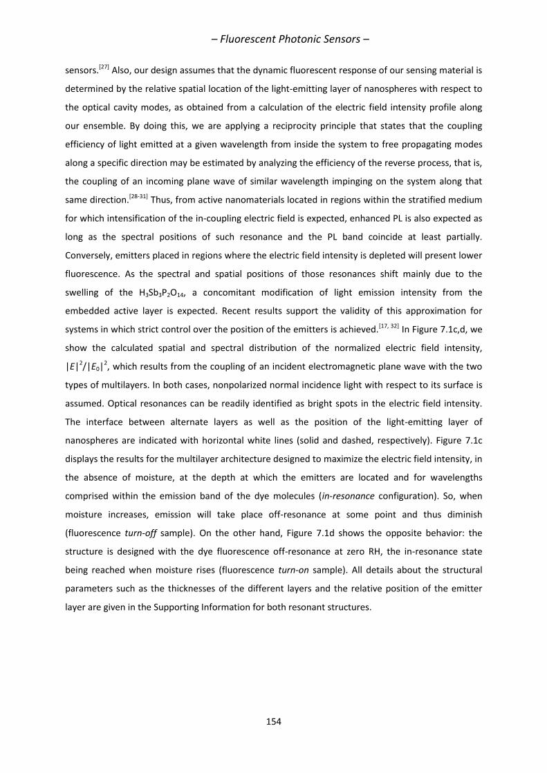
– Fluorescent Photonic Sensors –
154
sensors.[27] Also, our design assumes that the dynamic fluorescent response of our sensing material is
determined by the relative spatial location of the light-emitting layer of nanospheres with respect to
the optical cavity modes, as obtained from a calculation of the electric field intensity profile along
our ensemble. By doing this, we are applying a reciprocity principle that states that the coupling
efficiency of light emitted at a given wavelength from inside the system to free propagating modes
along a specific direction may be estimated by analyzing the efficiency of the reverse process, that is,
the coupling of an incoming plane wave of similar wavelength impinging on the system along that
same direction.[28-31] Thus, from active nanomaterials located in regions within the stratified medium
for which intensification of the in-coupling electric field is expected, enhanced PL is also expected as
long as the spectral positions of such resonance and the PL band coincide at least partially.
Conversely, emitters placed in regions where the electric field intensity is depleted will present lower
fluorescence. As the spectral and spatial positions of those resonances shift mainly due to the
swelling of the H3Sb3P2O14, a concomitant modification of light emission intensity from the
embedded active layer is expected. Recent results support the validity of this approximation for
systems in which strict control over the position of the emitters is achieved.[17, 32] In Figure 7.1c,d, we
show the calculated spatial and spectral distribution of the normalized electric field intensity,
|E|2/|E0|2, which results from the coupling of an incident electromagnetic plane wave with the two
types of multilayers. In both cases, nonpolarized normal incidence light with respect to its surface is
assumed. Optical resonances can be readily identified as bright spots in the electric field intensity.
The interface between alternate layers as well as the position of the light-emitting layer of
nanospheres are indicated with horizontal white lines (solid and dashed, respectively). Figure 7.1c
displays the results for the multilayer architecture designed to maximize the electric field intensity, in
the absence of moisture, at the depth at which the emitters are located and for wavelengths
comprised within the emission band of the dye molecules (in-resonance configuration). So, when
moisture increases, emission will take place off-resonance at some point and thus diminish
(fluorescence turn-off sample). On the other hand, Figure 7.1d shows the opposite behavior: the
structure is designed with the dye fluorescence off-resonance at zero RH, the in-resonance state
being reached when moisture rises (fluorescence turn-on sample). All details about the structural
parameters such as the thicknesses of the different layers and the relative position of the emitter
layer are given in the Supporting Information for both resonant structures.
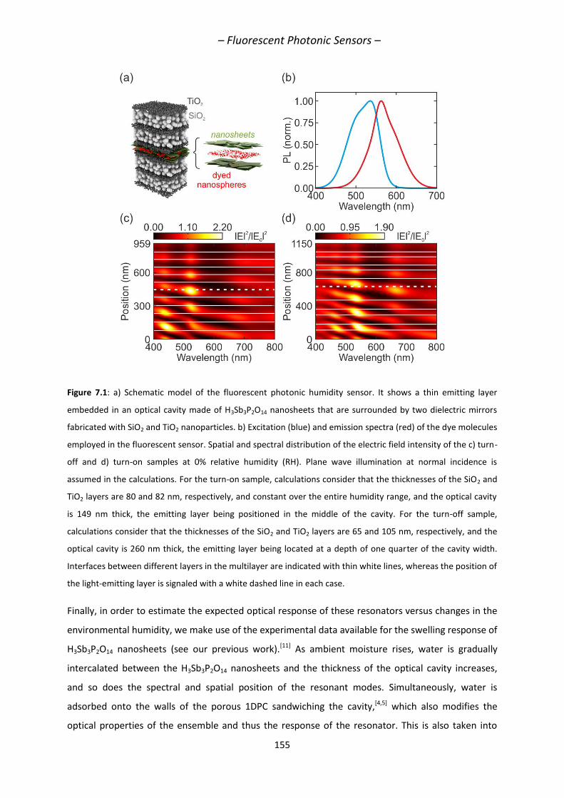
– Fluorescent Photonic Sensors –
155
Figure 7.1: a) Schematic model of the fluorescent photonic humidity sensor. It shows a thin emitting layer
embedded in an optical cavity made of H3Sb3P2O14 nanosheets that are surrounded by two dielectric mirrors
fabricated with SiO2 and TiO2 nanoparticles. b) Excitation (blue) and emission spectra (red) of the dye molecules
employed in the fluorescent sensor. Spatial and spectral distribution of the electric field intensity of the c) turn-
off and d) turn-on samples at 0% relative humidity (RH). Plane wave illumination at normal incidence is
assumed in the calculations. For the turn-on sample, calculations consider that the thicknesses of the SiO2 and
TiO2 layers are 80 and 82 nm, respectively, and constant over the entire humidity range, and the optical cavity
is 149 nm thick, the emitting layer being positioned in the middle of the cavity. For the turn-off sample,
calculations consider that the thicknesses of the SiO2 and TiO2 layers are 65 and 105 nm, respectively, and the
optical cavity is 260 nm thick, the emitting layer being located at a depth of one quarter of the cavity width.
Interfaces between different layers in the multilayer are indicated with thin white lines, whereas the position of
the light-emitting layer is signaled with a white dashed line in each case.
Finally, in order to estimate the expected optical response of these resonators versus changes in the
environmental humidity, we make use of the experimental data available for the swelling response of
H3Sb3P2O14 nanosheets (see our previous work).[11] As ambient moisture rises, water is gradually
intercalated between the H3Sb3P2O14 nanosheets and the thickness of the optical cavity increases,
and so does the spectral and spatial position of the resonant modes. Simultaneously, water is
adsorbed onto the walls of the porous 1DPC sandwiching the cavity,[4,5] which also modifies the
optical properties of the ensemble and thus the response of the resonator. This is also taken into
– Fluorescent Photonic Sensors –
156
account in our simulations. Our theoretical analysis reveals that the optical response of the ensemble
versus increasing moisture is expected to be mainly determined by the swelling of the H3Sb3P2O14
cavity, while the adsorption of water in the textural pores of the 1DPCs will have a lesser effect. In
Figure 7.2, we show the simulated evolution of the reflectance (R) (Figure 7.2a,b), electric field
intensity at the position of the emitter (Figure 7.2c,d), and the expected PL extracted from a model
architecture (Figure 7.2e,f) for the turn-off and turn-on sensors, respectively.
Figure 7.2: Calculated specular reflectance spectra as a function of the relative humidity for the a) turn-off and
b) turn-on samples. Electric field intensity at the emitting layer position of the c) turn-off and d) turn-on
sample. Estimated emitted intensity of the e) turn-off and f) turn-on sensor.
Sample Fabrication
In the next step, we experimentally realize the two photonic model architectures by sequentially
spin-coating the different layers they are composed of. First, alternate layers of SiO2 and TiO2
– Fluorescent Photonic Sensors –
157
nanoparticles were deposited from stable colloidal precursor suspensions to create the first
multilayer. Then, the humidity-responsive optical cavity was formed by spin-casting a suspension of
H3Sb3P2O14 exfoliated nanosheets directly onto it. Once a homogenous thin film of the predesigned
thickness was formed, a monolayer of light-emitting polystyrene nanospheres was deposited and
then covered by a new layer of H3Sb3P2O14. In this way, an embedded layer of emitters of ≈30 nm
thick is attained. Guided by our simulations, the light-emitting layer was positioned in the middle of
the optical cavity in the case of the fluorescence turn-off system, while for the turn-on sensor it was
located at a depth of one-quarter of that width. Finally, the second 1DPC was deposited onto the
humidity responsive layer. In order to enable the diffusion of water molecules through the dielectric
mirrors so that they can reach the middle layer, both mirrors were designed to be highly porous
(porosity of ≈ 50% in both silica and titania layers), and at the same time highly reflecting, which
results from the contrast between the average refractive indices of the SiO2 nanoparticle (nav = 1.3)
and TiO2 nanocrystal (nav = 1.8). The nav of the intermediate nanosheet layer changes from 1.61 to
1.52 when humidity increases from 2 to 99%, while its thickness is enlarged by a factor of 1.75.[11]
With these parameters, our calculations indicate that 1DPCs of five layers (starting and terminating
with the high refractive index TiO2 nanoparticle layer) are sufficient to attain well-defined cavity
modes. The experimental thicknesses achieved for the middle nanosheet layers, that is, the optical
cavities, were 140 ± 15 and 250 ± 15 nm (both measured at 0% RH in the scanning electron
microscope (SEM)) for the fluorescence turn-on and turn-off systems, respectively. These values are
in good agreement with the theoretical designs shown in Figure 7.1. Figure 7.3a shows a schematic
illustration of the sample fabrication. Secondary (left panels) and back-scattered (right panels)
electron microscopy images of the cross-sections of the two types of ensembles are displayed in
Figure 3b,c. The stratified structure can be readily seen in both cases. Since the layer of dyed
nanospheres has the lower atomic number (Z), its position can be easily identified in all images as a
darker thin line. Schemes of the two stratified media are superimposed to the back-scattered
electron images to ease the recognition of each type of slab.
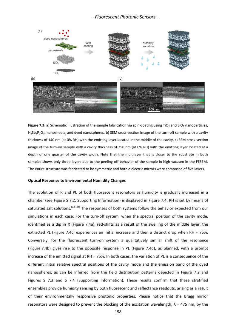
– Fluorescent Photonic Sensors –
158
Figure 7.3: a) Schematic illustration of the sample fabrication via spin-coating using TiO2 and SiO2 nanoparticles,
H3Sb3P2O14 nanosheets, and dyed nanospheres. b) SEM cross-section image of the turn-off sample with a cavity
thickness of 140 nm (at 0% RH) with the emitting layer located in the middle of the cavity. c) SEM cross-section
image of the turn-on sample with a cavity thickness of 250 nm (at 0% RH) with the emitting layer located at a
depth of one quarter of the cavity width. Note that the multilayer that is closer to the substrate in both
samples shows only three layers due to the peeling off behavior of the sample in high vacuum in the FESEM.
The entire structure was fabricated to be symmetric and both dielectric mirrors were composed of five layers.
Optical Response to Environmental Humidity Changes
The evolution of R and PL of both fluorescent resonators as humidity is gradually increased in a
chamber (see Figure S 7.2, Supporting Information) is displayed in Figure 7.4. RH is set by means of
saturated salt solutions.[33, 34] The responses of both systems follow the behavior expected from our
simulations in each case. For the turn-off system, when the spectral position of the cavity mode,
identified as a dip in R (Figure 7.4a), red-shifts as a result of the swelling of the middle layer, the
extracted PL (Figure 7.4c) experiences an initial increase and then a distinct drop when RH ≈ 75%.
Conversely, for the fluorescent turn-on system a qualitatively similar shift of the resonance
(Figure 7.4b) gives rise to the opposite response in PL (Figure 7.4d), as planned, with a prompt
increase of the emitted signal at RH ≈ 75%. In both cases, the variation of PL is a consequence of the
different initial relative spectral positions of the cavity mode and the emission band of the dyed
nanospheres, as can be inferred from the field distribution patterns depicted in Figure 7.2 and
Figures S 7.3 and S 7.4 (Supporting Information). These results confirm that these stratified
ensembles provide humidity sensing by both fluorescent and reflectance readouts, arising as a result
of their environmentally responsive photonic properties. Please notice that the Bragg mirror
resonators were designed to prevent the blocking of the excitation wavelength, λ = 475 nm, by the
– Fluorescent Photonic Sensors –
159
photonic stop band. As a reference, we measured the emission spectrum of the dyed nanospheres
located at the same depth within two nanosheet layers like the ones employed to build the photonic
fluorescent turn-on and turn-off systems, respectively, but without the two surrounding dielectric
mirrors. Figure 7.4e,f displays the evolution of the maximum PL intensity, normalized for the two
fluorescent humidity sensing ensembles (Figure 7.4e) and for the corresponding references
(Figure 7.4f). The PL of the references remains barely affected by the changes in humidity in the
environment, with both the photoexcitation and PL spectra essentially preserving the same shape
and intensity for the whole range of RH values tested. This comparison confirms that the
modification of the chemical environment of the dyed nanospheres as a result of water
intercalation—albeit responsive to humidity—is not enough by itself to produce the changes
observed in PL. We thus show that the fluorescence switching is in fact based on the tailored
interplay between photonic and emissive modes, that is, the stimuli-responsive photonic
environment acts on the fluorescent properties of the emitters, which in turn sensitively depends on
the level of moisture in the surrounding atmosphere. Notably, the fluorescence switching points can
be designed by the photonic architecture and placement of the emitters so as to address specific
sensing applications. For example, the turning-on/off point of the architectures presented herein
corresponds to a relative humidity of 75%, which renders such systems interesting for environmental
monitoring applications in the high humidity regime. This regime is particularly relevant for ambient
room monitoring, since mold formation in damp rooms starts around 75% RH, depending on the wall
material.[35,36] Finally, the reproducibility and stability of the response versus several cycles of
exposure to increasing and decreasing humidity were confirmed by performing these sequential
experiments several times. These results represent the first proof of concept of a fluorescent
photonic humidity sensor structure. Further studies with encapsulated dyes with a wider Stokes shift
would allow a higher accuracy on the detection of humidity changes.
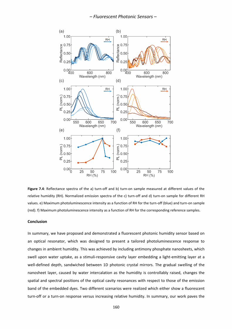
– Fluorescent Photonic Sensors –
160
Figure 7.4: Reflectance spectra of the a) turn-off and b) turn-on sample measured at different values of the
relative humidity (RH). Normalized emission spectra of the c) turn-off and d) turn-on sample for different RH
values. e) Maximum photoluminescence intensity as a function of RH for the turn-off (blue) and turn-on sample
(red). f) Maximum photoluminescence intensity as a function of RH for the corresponding reference samples.
Conclusion
In summary, we have proposed and demonstrated a fluorescent photonic humidity sensor based on
an optical resonator, which was designed to present a tailored photoluminescence response to
changes in ambient humidity. This was achieved by including antimony phosphate nanosheets, which
swell upon water uptake, as a stimuli-responsive cavity layer embedding a light-emitting layer at a
well-defined depth, sandwiched between 1D photonic crystal mirrors. The gradual swelling of the
nanosheet layer, caused by water intercalation as the humidity is controllably raised, changes the
spatial and spectral positions of the optical cavity resonances with respect to those of the emission
band of the embedded dyes. Two different scenarios were realized which either show a fluorescent
turn-off or a turn-on response versus increasing relative humidity. In summary, our work paves the
– Fluorescent Photonic Sensors –
161
way toward the development of a new generation of smart photonic devices that do not only display
a gradual reflected or transmitted color variation, but also additionally feature a tailorable
fluorescent signal read-out. As such, specific analytes can sensitively be traced by means of a distinct
luminescent signal change in response to variations in analyte concentration, which bodes well for
the development of versatile photonic sensing platforms compatible with luminescence detection
schemes.
7.6 EXPERIMENTAL SECTION
Numerical Calculations
The optical response of the photonic structures was calculated using a full wave vector model based
on the transfer matrix formalism. The PL was estimated by multiplying the field intensity at the
position of the organic dye molecules with the emission spectrum of the dye molecules deposited on
glass.
Synthesis of the H3Sb3P2O14 Nanosheets
K3Sb3P2O14 was prepared in a two-step solid-state reaction.[37] The precursors KNO3 (99%, Merck),
Sb2O3 (99.6 %, Alfa Aesar), and NH4H2PO4 (98%+, Acros Organics) were ground in a stoichiometric
ratio and heated up first to 350 °C for 12 h with a heating rate of 5 °C min−1. In a second step, the
mixture was heated to 950 °C for 12 h with a heating rate of 5 °C min−1. To obtain H3Sb3P2O14,
K3Sb3P2O14 was treated with 8 m HNO3 (250 mL, diluted 65 wt%, Merck) overnight, filtrated, washed
with ethanol, and dried at room temperature. This treatment was repeated once more to complete
the ion exchange reaction.[11] For exfoliation, H3Sb3P2O14 was vigorously stirred overnight in pure
water (7.3 mmol L−1). The resulting colloidal suspension was then centrifuged at 3000 rpm for 30 min
to remove non-exfoliated bulk material. The supernatant, which consists mainly of exfoliated single-
layer nanosheets, was collected and centrifuged at 18 000 rpm for 30 min to yield the nanosheet
pellet. The gel-like, colorless wet aggregate was dried at 100 °C.
Preparation of the Colloidal Suspensions
The dried nanosheets were redispersed in a water-ethanol mixture (60 wt% ethanol) with a
concentration of 21 mmol L−1. To ensure homogeneity and the complete exfoliation into single-
layered nanosheets, the suspension was sonicated for 2 h. TiO2 nanoparticles were synthesized using
a procedure described elsewhere.[5] Colloidal SiO2 nanoparticles with a particle diameter of 30 nm
were purchased from Sigma Aldrich (LUDOX-TMA). Both suspensions were diluted with methanol to
3.4 and 2.3 wt%, respectively, and directly taken for layer preparation after 10 min sonication.
– Fluorescent Photonic Sensors –
162
Fabrication of the Photonic Structures
All layers comprising the photonic resonators were fabricated via spin-coating. Zero-fluorescent
microscope slides (Proscitech, cut to 2 × 2 cm2 pieces) employed as substrates were cleaned with
oxygen plasma. Porous dielectric mirrors made of five layers were deposited via spin-coating. SiO2
and TiO2 colloids were deposited using 6000 rpm rotation speed, with an acceleration of 5000 rpm
s−1 for 1 min, the first and the last layers of the stack correspond to the high refractive index material,
that is, TiO2. Afterward, the samples were heated for 15 min at 80 °C before the cavity deposition.
The cavity was composed of H3Sb3P2O14, which was deposited in 6/8 steps (turn-off/on sample).
Spinning conditions for each deposition step were 3000 rpm and 5000 rpm s−1. The samples were
heated for 15 min at 80 °C after each deposition step. The position of the emitters was determined
during the cavity fabrication. After three (turn-off sample) or two (turn-on sample) nanosheet
deposition steps, the commercially available Firefli Fluorescent Red dyed nanospheres (R25, Thermo
Fisher Scientific) were deposited without dilution or further purification directly on top of the
nanosheets using 3000 rpm and 5000 rpm min−1 for 1 min. To remove the excess of emitters,
samples were washed with pure methanol at 3000 rpm and 5000 rpm min−1. After heating again at
80 °C for 15 min, the rest of the cavity was deposited on top of the emitter layer and another 3/6
deposition steps (turn-off/on sample) were applied, respectively. Finally, a porous 1DPC composed of
five layers was deposited on top of the cavity in the same fashion as described above. Finally, the
samples were heated at 80 °C for 30 min.
Optical Characterization
Specular reflectance spectra were measured from areas of 1 × 1 mm2 using a fiber coupled
spectrometer (USB2000+, Ocean Optics) attached to a microscope (DM2500, Leica). To obtain the
reflectance changes with relative humidity change, dielectric mirrors stacks were kept over saturated
salt solutions at around 25 °C in a stainless steel chamber with a transparent glass window.[31,32]
Fluorescence measurements were carried out using a commercial spectrofluorometer (Fluorolog-3
Horiba Jobin Yvon). The photoemission spectra were measured from 450 to 700 nm with a step of 3
nm using an excitation wavelength of 440 ± 3 nm. All this photoluminescence characterization was
performed collecting emitted light at an angle of 11.25°. Spectroscopic ellipsometry and porosimetry
measurements were carried out with a Sopra PS-1000 SAM, whereby the sample was equilibrated at
all water vapor relative pressure values for 15 min. The resulting spectra were fitted with the
software Sopra SAE applying the Cauchy–Lorentz model. The nanoparticle layer thickness was
estimated to be constant and only the refractive indices were fitted for the whole relative pressure
range. For the nanosheet thin films, both the layer thickness and the refractive index were fitted.
– Fluorescent Photonic Sensors –
163
Before all measurements, the nanoparticle samples were heated for at least 30 min at 200 °C and the
nanosheet thin films for 30 min at 80 °C in vacuum to make sure that the pores are empty.
Structural Characterization
Field-emission SEM cross-section images were collected by a Zeiss Merlin working at 1.5 kV using
both back scattered as well as secondary electrons.
7.7 ACKNOWLEDGEMENTS
K.S. and A.J.-S. contributed equally to this work. The authors thank Viola Duppel for FESEM
measurements and Dr. Mauricio E. Calvo for his help with the spectroscopic analysis of light reflected
under different ambient conditions. Financial support granted by the Max Planck Society, the
University of Munich (LMU), the Center for NanoScience (CeNS), the Deutsche
Forschungsgemeinschaft (DFG) through the Cluster of Excellence Nanosystems Initiative Munich
(NIM), the European Research Council under the European Union's Seventh Framework Programme
(FP7/2007-2013)/ERC Grant Agreement No. 307081 (POLIGHT), and the Spanish Ministry of Economy
and Competitiveness under grant MAT2014-54852-R is gratefully acknowledged. A.J.-S.
acknowledges the Spanish Ministry of Economy and Competitiveness for funding through an FPI
program under the project MAT2011-23593.
7.8 REFERENCES
[1] H. S. Jung, P. Verwilst, W. Y. Kim, J. S. Kim, Chem. Soc. Rev. 2016, 45, 1242.
[2] E+E ELEKTRONIK Gesellschaft m.b.H., commercially available humidity sensors,
http://www.epluse.com/en/products/humidity-instruments/humidity-sensor (accessed: April
2017).
[3] Vaisala, commercially available humidity sensors,
http://www.vaisala.com/en/products/humidity/Pages/default.aspx (accessed: April 2017).
[4] M. C. Fuertes, S. Colodrero, G. Lozano, A. R. González-Elipe, D. Grosso, C. Boissière, C. Sánchez,
G. J. d. A. A. Soler-Illia, H. Míguez, J. Phys. Chem. C 2008, 112, 3157.
[5] S. Colodrero, M. Ocaña, A. R. Gonzalez-Elipe, H. Miguez, Langmuir 2008, 24, 9135.
[6] N. Hidalgo, M. E. Calvo, H. Miguez, Small 2009, 5, 2309.
[7] F. M. Hinterholzinger, A. Ranft, J. M. Feckl, B. Ruhle, T. Bein, B. V. Lotsch, J. Mater. Chem. 2012,
22, 10356.
[8] E. Tian, J. Wang, Y. Zheng, Y. Song, L. Jiang, D. Zhu, J. Mater. Chem. 2008, 18, 1116.
[9] R. Xuan, Q. Wu, Y. Yin, J. Ge, J. Mater. Chem. 2011, 21, 3672.
– Fluorescent Photonic Sensors –
164
[10] H. Kim, J. Ge, J. Kim, S. E. Choi, H. Lee, H. Lee, W. Park, Y. Yin, S. Kwon, Nat. Photon. 2009, 3, 534.
[11] K. Szendrei, P. Ganter, O. Sanchez-Sobrado, R. Eger, A. Kuhn, B. V. Lotsch, Adv. Mater. 2015, 27,
6341.
[12] P. Ganter, K. Szendrei, B. V. Lotsch, Adv. Mater. 2016, 28, 7436.
[13] I. Pavlichenko, E. Broda, Y. Fukuda, K. Szendrei, A. K. Hatz, G. Scarpa, P. Lugli, C. Brauchle, B. V.
Lotsch, Mater. Horiz. 2015, 2, 299.
[14] A. T. Exner, I. Pavlichenko, D. Baierl, M. Schmidt, G. Derondeau, B. V. Lotsch, P. Lugli, G. Scarpa,
Laser Photon. Rev. 2014, 5, 726.
[15] O. Sanchez-Sobrado, G. Lozano, M. E. Calvo, A. Sánchez-Iglesias, L. M. Liz-Marzán, H. Míguez,
Adv. Mater. 2011, 23, 2108.
[16] A. Jimenez-Solano, C. Lopez-Lopez, O. Sanchez-Sobrado, J. M. Luque, M. E. Calvo, C. Fernandez-
Lopez, A. Sanchez-Iglesias, L. M. Liz-Marzán, H. Miguez, Langmuir 2012, 28, 9161.
[17] A. Jimenez-Solano, J. F. Galisteo-Lopez, H. Miguez, Small 2015, 11, 2727.
[18] O. Sanchez-Sobrado, M. E. Calvo, N. Nuñez, M. Ocaña, G. Lozano, H. Miguez, Nanoscale 2010, 2,
936.
[19] D. P. Puzzo, F. Scotognella, M. Zavelani-Rossi, M. Sebastian, A. J. Lough, I. Manners, G. Lanzani,
R. Tubino, G. A. Ozin, Nano Lett. 2009, 9, 4273.
[20] F. Scotognella, D. P. Puzzo, A. Monguzzi, D. S. Wiersma, D. Maschke, R. Tubino, G. A. Ozin, Small
2009, 5, 2048.
[21] M. G. Choi, M. H. Kim, H. J. Kim, J. E. Park, S. K. Chang, Bull. Korean Chem. Soc. 2007, 28, 1818.
[22] G. Men, G. Zhang, C. Liang, H. Liu, B. Yang, Y. Pan, Z. Wang, S. Jiang, Analyst 2013, 138, 2847.
[23] S. Pal, M. Mukherjee, B. Sen, S. Lohara, P. Chattopadhyay, RSC Adv. 2014, 4, 21608.
[24] S. Colodrero, M. Ocaña, H. Míguez, Langmuir 2008, 24, 4430.
[25] J. Homola, S. S. Yeea, G. Gauglitz, Sens. and Actuators B: Chem. 1999, 54, 3.
[26] R. J. Photton, Rep. Prog. Phys. 2004, 67, 717.
[27] O. T. A. Janssen, A J. H. Wachters, H. P. Urbach, Opt. Express 2010, 18, 24522.
[28] S. Zhang, E. R. Martins, A. G. Diyaf, J. I. B. Wilson, G. A. Turnbull, I. D. W. Samuel, Synth. Met.
2015, 205, 127.
[29] G. Lozano, D. J. Louwers, S. R. K. Rodríguez, S. Murai, O. T. A. Jansen, M. A. Verschuuren, J.
Gómez Rivas, Light Sci. Appl. 2013, 2, e66
[30] M. Ramezani, G. Lozano, M. A. Verschuuren, J. Gómez Rivas, Phys. Rev. B 2016, 94, 125406.
[31] P. W. Winston, D. H. Bates, Ecology 1960, 41, 232.
[32] L. Greenspan, J. Res. Nat. Bur. Stand. 1977, 81A, 89.
[33] J. Vučković, D. Fattal, C. Santori, G. S. Solomon, Y. Yamamoto, Appl. Phys. Lett. 2003, 82, 3596.

– Fluorescent Photonic Sensors –
165
[34] O. O. Hänninen, Fundamentals of mold growth in indoor environments and strategies for healthy
living (Eds.: O. C. G. Adan, R. A. Samson), Wageningen Academic Publishers, Wageningen, 2011,
pp. 277.
[35] Y. Piffard, A. Lachgar, M. Tournoux, J. Solid State Chem. 1985, 58, 253.

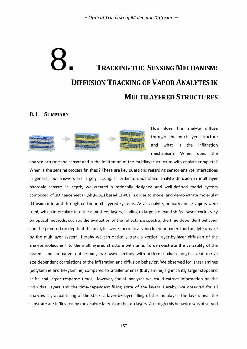
– Optical Tracking of Molecular Diffusion –
167
8. TRACKING THE SENSING MECHANISM:
DIFFUSION TRACKING OF VAPOR ANALYTES IN
MULTILAYERED STRUCTURES
8.1 SUMMARY
How does the analyte diffuse
through the multilayer structure
and what is the infiltration
mechanism? When does the
analyte saturate the sensor and is the infiltration of the multilayer structure with analyte complete?
When is the sensing process finished? These are key questions regarding sensor-analyte interactions
in general, but answers are largely lacking. In order to understand analyte diffusion in multilayer
photonic sensors in depth, we created a rationally designed and well-defined model system
composed of 2D nanosheet (H3Sb3P2O14) based 1DPCs in order to model and demonstrate molecular
diffusion into and throughout the multilayered systems. As an analyte, primary amine vapors were
used, which intercalate into the nanosheet layers, leading to large stopband shifts. Based exclusively
on optical methods, such as the evaluation of the reflectance spectra, the time-dependent behavior
and the penetration depth of the analytes were theoretically modeled to understand analyte uptake
by the multilayer system. Hereby we can optically track a vertical layer-by-layer diffusion of the
analyte molecules into the multilayered structure with time. To demonstrate the versatility of the
system and to carve out trends, we used amines with different chain lengths and derive
size-dependent correlations of the infiltration and diffusion behavior. We observed for larger amines
(octylamine and hexylamine) compared to smaller amines (butylamine) significantly larger stopband
shifts and larger response times. However, for all analytes we could extract information on the
individual layers and the time-dependent filling state of the layers. Hereby, we observed for all
analytes a gradual filling of the stack, a layer-by-layer filling of the multilayer: the layers near the
substrate are infiltrated by the analyte later than the top layers. Although this behavior was observed

– Optical Tracking of Molecular Diffusion –
168
for all analytes, significant differences in the delay of the filling of the layers are observed, which
were accompanied by large differences of the swelling of the individual layers.
Katalin Szendrei-Temesi planned the project, designed and fabricated the 1DPCs, performed the
optical measurements, edited the figures and wrote the manuscript. Alberto Jiménez-Solano
performed the theoretical calculations in order to reproduce the analyte diffusion to understand the
diffusion mechanism, assisted with the optical measurements, wrote the manuscript and edited the
figures.
– Optical Tracking of Molecular Diffusion –
169
8.2 TRACKING VERTICAL MOLECULAR DIFFUSION INTO 1-DIMENSIONAL
PHOTONIC CRYSTALS
Katalin Szendrei-Temesi,* Alberto Jiménez-Solano,* Bettina V. Lotsch
* These authors contributed equally to this work.
To be submitted.
8.3 ABSTRACT
By virtue of their structural color, Photonic crystals have emerged as attractive colorimetric sensors.
Their ease of use as well as their inexpensive fabrication have made these devices a successful
commercial case. Despite their advanced development stage, insights into the sensing mechanism, in
particular the diffusion of analytes through photonic multilayer systems, are largely lacking, but are
key for their design. Herein, we use bio-inspired 1D Photonic Crystals based on swellable 2D
nanosheets and dielectric nanoparticles as a model system and track the time-dependent
intercalation of amine molecules into the structure by optical spectroscopy and theoretical
modelling. We follow the consecutive swelling of the layers in real-time and show that with
increasing analyte size, both colour shifts and diffusion times increase significantly, while infiltration
of the multilayer system is complete in a few seconds. The methodology developed here introduces a
new method to study diffusion processes in complex photonic nanostructures and thin films based
on a simple optical readout.
8.4 INTRODUCTION
The trend towards digitalization and automation, prominently represented by the Internet of Things
(IoT),[1] comes along with an increasing demand for novel sensing schemes, miniaturization of
sensors, and sensor fusion.[2-4] This renaissance of sensing technology requires a deep understanding
of complex sensing processes, such as the interaction of gaseous analytes with the responsive sensor
architecture in environmental sensors.[5, 6] It is thus key to understand the time-resolved sensor
response to analyte exposure, diffusion, as well as local analyte concentration and saturation.
Photonic vapor sensors are unique sensing platforms in that they offer a colorimetric read-out whilst
operating in a label free fashion[7] without requiring complex electric wiring.[8-10] In recent years, 1D
Photonic Crystals (1DPCs),[10, 11] which are periodic arrays of materials with different dielectric
constants, emerged as versatile sensing platforms[12-15] showing well-defined optical properties, a
simple structure and ease of integration. Besides, 1DPCs are compatible with a vast amount of
stimuli-responsive materials that can be integrated as functional building blocks, including dielectric
– Optical Tracking of Molecular Diffusion –
170
nanoparticles,[13, 16] functional nanoparticles[17-[19] mesoporous structures,[14] 2D materials,[8, 20-23] or
polymeric multilayers.[24, 25] In addition, 1DPCs have been used to detect and host guest molecules,
thereby showing structural flexibility,[26, 27] emissive properties,[28-30] and superior sensing
characteristics in terms of analyte selectivity,[9, 19, 31] sensitivity,[8, 9, 20, 24, 32, 33] response times,[8]
compact readout[10, 34, 35] and miniaturization in a lab-on-a-chip fashion.[36] The knowledge of
time-resolved analyte infiltration into such multilayer structures is key to understand the kinetics of
analyte propagation and, hence, response times, the homogeneity of analyte impregnation, and the
impact of interfaces. Insights into such microscopic processes would help to design and optimize the
sensing architecture, especially with regards to chemical functionalization and modification.[37-40]
Several approaches were presented in the literature to analyze the diffusion of vaporous analytes
into porous periodic multilayers[37] and optical cavity structures.[41] However, all approaches used
spatially averaging techniques and none of them was able to track analyte diffusion in a spatially and
temporally resolved fashion. In addition, correlation of analyte diffusion with material specific
host-guest interactions remains a formidable task.
In this work, we tackle this challenge by employing a stimuli-responsive 1DPC based on swellable 2D
antimony phosphate H3Sb3P2O14 nanosheets (NSs)[8, 42, 43] and TiO2 nanoparticles (NPs)[8] to track
time-resolved molecular diffusion into the multilayer system (for the fabrication details see
Experimental Section, Supporting Information). While being structurally simple and solution-
processable, 1DPCs feature well-defined optical properties which are easy to characterize.[44, 45] To
develop 1DPCs into a powerful detection platform, the selection of stimuli-responsive materials
showing pronounced environmentally induced dimensional changes and changes in their dielectric
properties is decisive. Thus, the material choice is crucial and the integrated NS layers show
significant swelling behavior upon intercalation of analytes, such as water or volatile organic
compounds;[9, 30] in addition, the RI contrast between NS and NP layers increases upon analyte
uptake, as does the reflectance intensity,[8] which is favorable for precise optical analysis.
To be able to track the time-dependent diffusion, we use primary straight-chain amines as the
analytes, which have been shown to intercalate into 2D NSs and to induce a pronounced swelling of
these layers.[46] The study of adsorption and vertical diffusion of analytes into the periodic multilayer
crucially depends on the size, polarity and chemical affinity of the analyte to the host layer. Amines
interact strongly with the interlayer protons of the solid acid H3Sb3P2O14 and at the same time show
high molecular and chemical variety. They are able to form ammonium ions with the protons and are
thus trapped between the NSs, causing the NS layers to swell to a different extent depending on their
molecular size.[46-48] This layer swelling translates into changes in the structural color,[44] which can be
detected with conventional optical methods. By applying these different amines with trending
– Optical Tracking of Molecular Diffusion –
171
molecular sizes and chemical properties, we were able to optically track molecular diffusion within
the 1DPC. By theoretical analysis of the time-dependent reflectance measurements using the
Transfer Matrix Method (TMM)[49, 50] combined with Genetic Algorithms (GAs),[51] we were able to
extract information about the temporal evolution of the thickness changes of each NS single layer
within the structure upon analyte exposure. Evaluation of the latter allows us to extract accurate
information about the layer thicknesses and refractive index (RI) of the individual layers,[52] which is
crucial for diffusion studies.
Translating information at the macroscopic level (i.e. color changes) into microscopic information,
this study delivers basic insights into the photonic sensing mechanism at the molecular level. In
addition, amine intercalation may be used to chemically modify the sensor and tailor its response as
shown previously.[46] This study delivers the framework for understanding such time-dependent
intercalation processes aiming at sensor functionalization to tailor host-guest interactions and to
rationally tune the sensor response.
8.5 RESULTS AND DISCUSSION
In Figure 8.1, the scanning electron microscopy (SEM) cross section image shows a 1DPC comprising
11 layers of alternatingly deposited TiO2 NPs and H3Sb3P2O14 NSs. The homogenous stacking and
clean interfaces between the two materials is evidenced by the periodic distribution of the sheet-like
and porous morphology in the secondary electron image (Figure 8.1a) and by the material contrast in
the back-scattered electron image (Figure 8.1b).
In this work, we study the time-dependent adsorption of primary straight-chain amines with an even
number of carbon atoms: butyl- (C4), hexyl- (C6) and octylamine (C8) and investigate the trends
arising among the amines with different chain lengths (Figure 8.1c). For consistency, we use an
ethanol-amine solution with an amine concentration of 1 M in order to facilitate the evaporation of
the larger amines and keep the evaporation rates as comparable as possible. As depicted in
Figure 8.1d, the 1DPC was first exposed to the diluted amine through a hole in the glass plate so as to
ensure that we exclusively detect the vertical diffusion of the analytes into the stack vertical to the
substrate. Subsequently, the reflectance of the ensemble was monitored in situ as the amines travel
along the structure, whereby the reflectance measurements were performed above the hole,
ensuring a homogenous exposure of the monitored area. In addition, to keep all measurements
comparable, we used different spots of the same sample for all three sets of measurements.
Afterwards, the structure and the reflectance spectra were modeled theoretically.
– Optical Tracking of Molecular Diffusion –
172
The initial reflectance maximum at λ ≈ 460 nm was measured (Figure S 8.1), which corresponds to
the initial optical response of the sample at ambient conditions (t = 0ambient). After exposure to the
ethanol-amine mixture, a fast reflectance peak shift, ∆λ ≈ 40 nm, is observable for all three systems,
which is accompanied by an increase in reflectance intensity of ∆R ≈ 10%. By fitting the initial and
final spectra after this shift (Figure S 8.1), we correlate the reflectance peak shift to the filling of the
structure with ethanol vapor, which is available in excess in the analyte mixture. The magnitude of
this initial shift is similar for all three cases, which further confirms that this displacement
corresponds to the ethanol uptake of the entire sample. For this reason, we define the time starting
point as t = 0EtOH, where ethanol already infiltrated the structure. In the fitting procedure, we
optimized all layer thicknesses separately, as during the fabrication via spin-coating layer thickness
variations are common.[15] Further, for the starting point (t = 0EtOH), we optimized the effective RI for
each material, but restricted it to be equal for the same material in different layers.
In the next step, we analyzed the reflectance spectra monitoring the amine intercalation at t > 0EtOH.
The time dependent shifts of the reflectance peak were plotted and fitted for ≈ 30 spectra from the
t = 0EtOH spectrum till the saturation level. Similar to the previous fitting, the layer thicknesses were
optimized separately for each individual layers. The RI of the TiO2 layers was assumed to be constant,
considering that after the filling with ethanol in the initial step, no large changes are expected. The
effective RI of the NS layers was estimated by taking into account that the intercalation of the
analytes and swelling leads to a decrease in RI of the NS layer. Hence, the RI can be extracted from
the optical spectra by applying the volumetric effective medium approximation theory,[53, 54] using
the filling fraction of the NS layers as the ratio between the layer thickness at t = 0EtOH and at time t
for each NS layer, m:
(1)
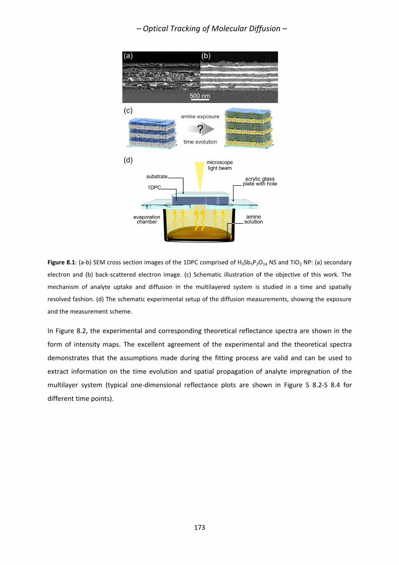
– Optical Tracking of Molecular Diffusion –
173
Figure 8.1: (a-b) SEM cross section images of the 1DPC comprised of H3Sb3P2O14 NS and TiO2 NP: (a) secondary
electron and (b) back-scattered electron image. (c) Schematic illustration of the objective of this work. The
mechanism of analyte uptake and diffusion in the multilayered system is studied in a time and spatially
resolved fashion. (d) The schematic experimental setup of the diffusion measurements, showing the exposure
and the measurement scheme.
In Figure 8.2, the experimental and corresponding theoretical reflectance spectra are shown in the
form of intensity maps. The excellent agreement of the experimental and the theoretical spectra
demonstrates that the assumptions made during the fitting process are valid and can be used to
extract information on the time evolution and spatial propagation of analyte impregnation of the
multilayer system (typical one-dimensional reflectance plots are shown in Figure S 8.2-S 8.4 for
different time points).
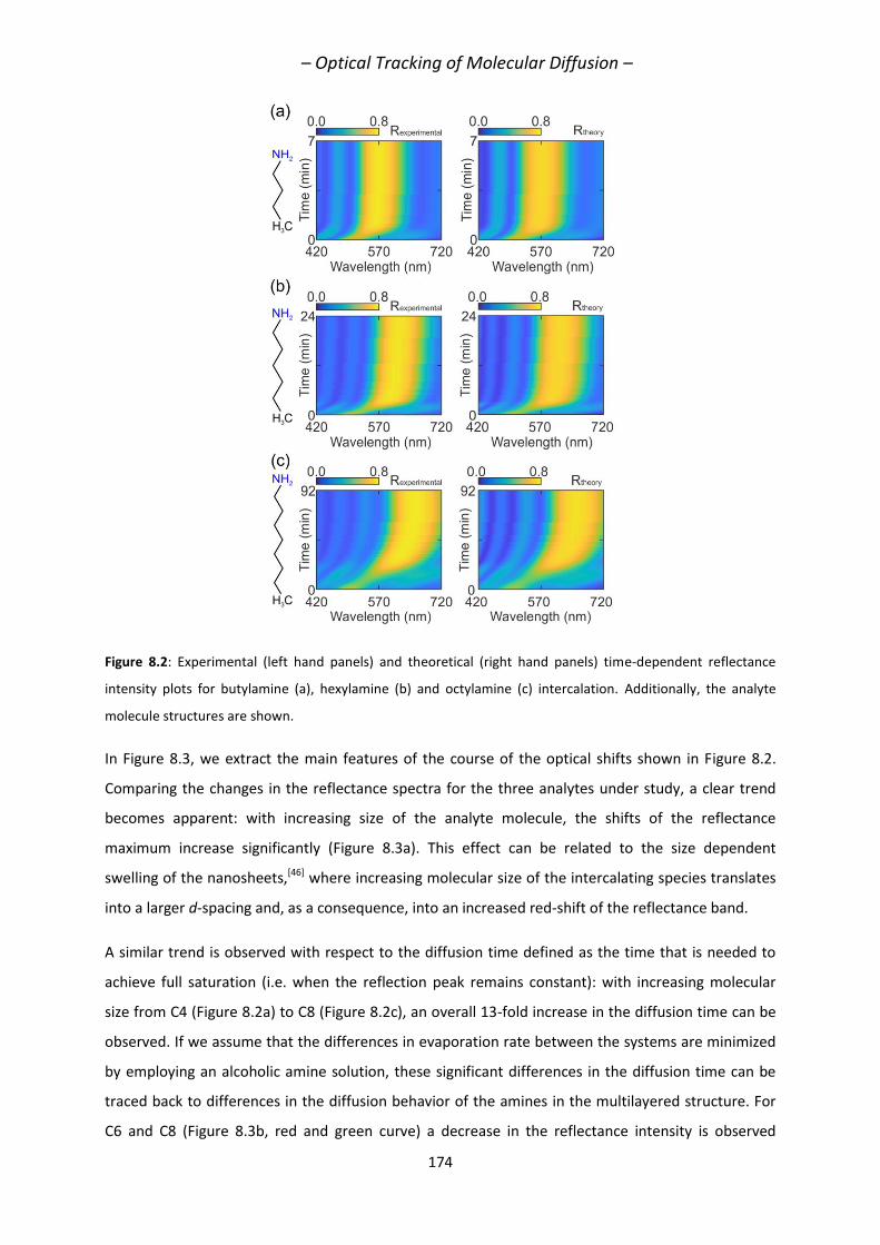
– Optical Tracking of Molecular Diffusion –
174
Figure 8.2: Experimental (left hand panels) and theoretical (right hand panels) time-dependent reflectance
intensity plots for butylamine (a), hexylamine (b) and octylamine (c) intercalation. Additionally, the analyte
molecule structures are shown.
In Figure 8.3, we extract the main features of the course of the optical shifts shown in Figure 8.2.
Comparing the changes in the reflectance spectra for the three analytes under study, a clear trend
becomes apparent: with increasing size of the analyte molecule, the shifts of the reflectance
maximum increase significantly (Figure 8.3a). This effect can be related to the size dependent
swelling of the nanosheets,[46] where increasing molecular size of the intercalating species translates
into a larger d-spacing and, as a consequence, into an increased red-shift of the reflectance band.
A similar trend is observed with respect to the diffusion time defined as the time that is needed to
achieve full saturation (i.e. when the reflection peak remains constant): with increasing molecular
size from C4 (Figure 8.2a) to C8 (Figure 8.2c), an overall 13-fold increase in the diffusion time can be
observed. If we assume that the differences in evaporation rate between the systems are minimized
by employing an alcoholic amine solution, these significant differences in the diffusion time can be
traced back to differences in the diffusion behavior of the amines in the multilayered structure. For
C6 and C8 (Figure 8.3b, red and green curve) a decrease in the reflectance intensity is observed
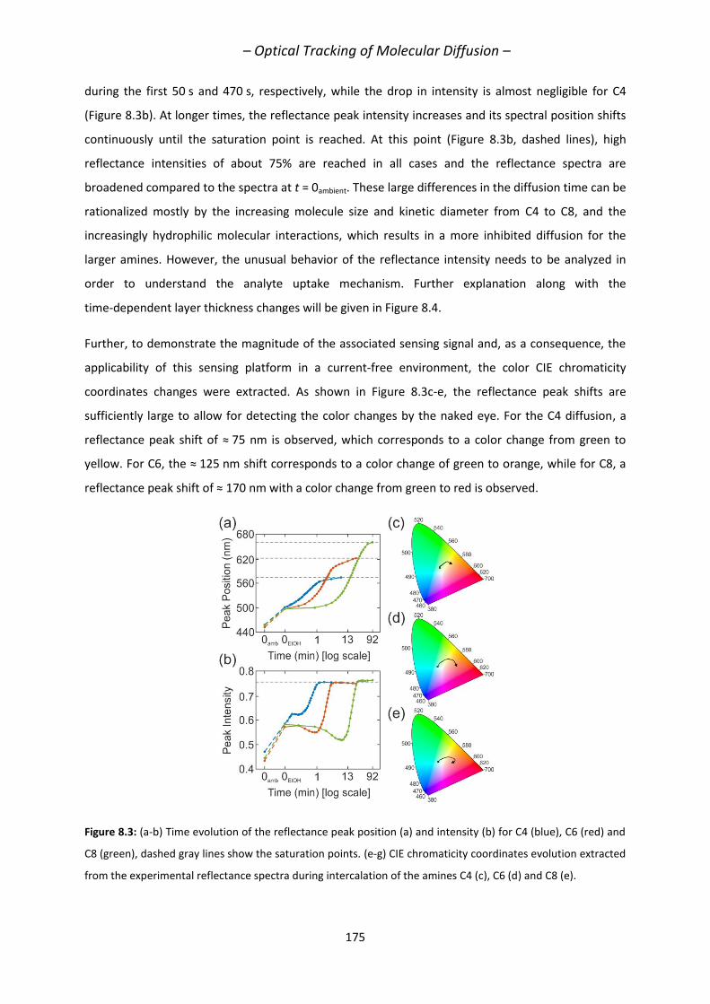
– Optical Tracking of Molecular Diffusion –
175
during the first 50 s and 470 s, respectively, while the drop in intensity is almost negligible for C4
(Figure 8.3b). At longer times, the reflectance peak intensity increases and its spectral position shifts
continuously until the saturation point is reached. At this point (Figure 8.3b, dashed lines), high
reflectance intensities of about 75% are reached in all cases and the reflectance spectra are
broadened compared to the spectra at t = 0ambient. These large differences in the diffusion time can be
rationalized mostly by the increasing molecule size and kinetic diameter from C4 to C8, and the
increasingly hydrophilic molecular interactions, which results in a more inhibited diffusion for the
larger amines. However, the unusual behavior of the reflectance intensity needs to be analyzed in
order to understand the analyte uptake mechanism. Further explanation along with the
time-dependent layer thickness changes will be given in Figure 8.4.
Further, to demonstrate the magnitude of the associated sensing signal and, as a consequence, the
applicability of this sensing platform in a current-free environment, the color CIE chromaticity
coordinates changes were extracted. As shown in Figure 8.3c-e, the reflectance peak shifts are
sufficiently large to allow for detecting the color changes by the naked eye. For the C4 diffusion, a
reflectance peak shift of ≈ 75 nm is observed, which corresponds to a color change from green to
yellow. For C6, the ≈ 125 nm shift corresponds to a color change of green to orange, while for C8, a
reflectance peak shift of ≈ 170 nm with a color change from green to red is observed.
Figure 8.3: (a-b) Time evolution of the reflectance peak position (a) and intensity (b) for C4 (blue), C6 (red) and
C8 (green), dashed gray lines show the saturation points. (e-g) CIE chromaticity coordinates evolution extracted
from the experimental reflectance spectra during intercalation of the amines C4 (c), C6 (d) and C8 (e).
– Optical Tracking of Molecular Diffusion –
176
While the above analysis reveals details of the kinetics of analyte diffusion into the multilayer
ensemble, we can go one step further and deconvolute the reflectance changes into the local analyte
distribution and, hence, gain spatio-temporal information of the sensing process. To this end, we
extracted the single layer thickness changes of each NS layer during the intercalation process and
analyzed them with respect to the elapsed time. Using this procedure, the overall spectral evolution
is translated into the filling state of the individual layers, yielding further insights into the molecular
diffusion and adsorption mechanism. Figure 8.4 show the results of the fittings, where for all plots
layer #1 refers to the first NS layer closest to the air/sample interface through which the analyte is
introduced into the multilayer system, and layer #5 is the NS layer close to the substrate. The TiO2 NP
layer thickness and RI are both assumed to be constant after the saturation with ethanol at t = 0EtOH.
For C4 (Figure 8.4a and Table S 8.1), layers #1 and #2 behave almost similar, and for both an
immediate swelling by ≈ 27 nm is observed after the amines reach the multilayered structure. Layers
#3 and #4 are delayed by ≈ 4 s and show the same extent of layer swelling, and finally the growth of
layer #5 starts after ≈ 20 s, but the extent of the swelling is similar to the other layers. After a short
time, ≈ 77 s, the layer thicknesses reach a collective value and swell together until the saturation
after 7 min and a swelling of 31 nm is reached. For C6 (Figure 8.4b and Table S1), the time delay by
which the layers consecutively swell is more extreme. The layer thickness increase of #1 and #2 starts
immediately, and the other layers follow this behavior at longer times: #3 at 30 s, #4 at 50 s and #5 at
100 s. After 6 min, all layers have nearly reached a collective swollen state (30 to 52 nm) and only a
further layer thickness increase of ≈ 7 nm each is observed. While for C4 the layers swell by
approximately 31 nm each, the maximum swelling of the individual layers reaches a value between
49 and 57 nm each for C6 in a total diffusion time of 24 min, which can be lead back to the increased
molecular size of C6 compared to C4. Similarly, the larger molecular size is also responsible for the
slower diffusion times. This trend continues for C8 (Figure 8.4c and Table S1), where the swelling of
the individual layer diverges even more with time: #1 and #2 start to grow immediately, while #3
starts at 280 s, #4 at 470 s and #5 at 840 s. The abrupt growth values correspond to an individual
layer swelling of all layers of 40 nm. Contrary to the previous systems, the swelling procedure is not
finished after the growth of layer #5, but the layers collectively grow more, and a total layer swelling
of all individual layers of ≈ 60-72 nm in a total diffusion time of 92 min is reached. These values fit
well with the trends of the previously reported systems.[46, 48]
To put these findings into perspective, we rationalize the observed time evolution of the multilayer
system based on the host-guest interactions between ethanol, amine and the NS host layers
(Figure 8.4d). In all cases, an initial homogenous reflectance peak shift is observed (between
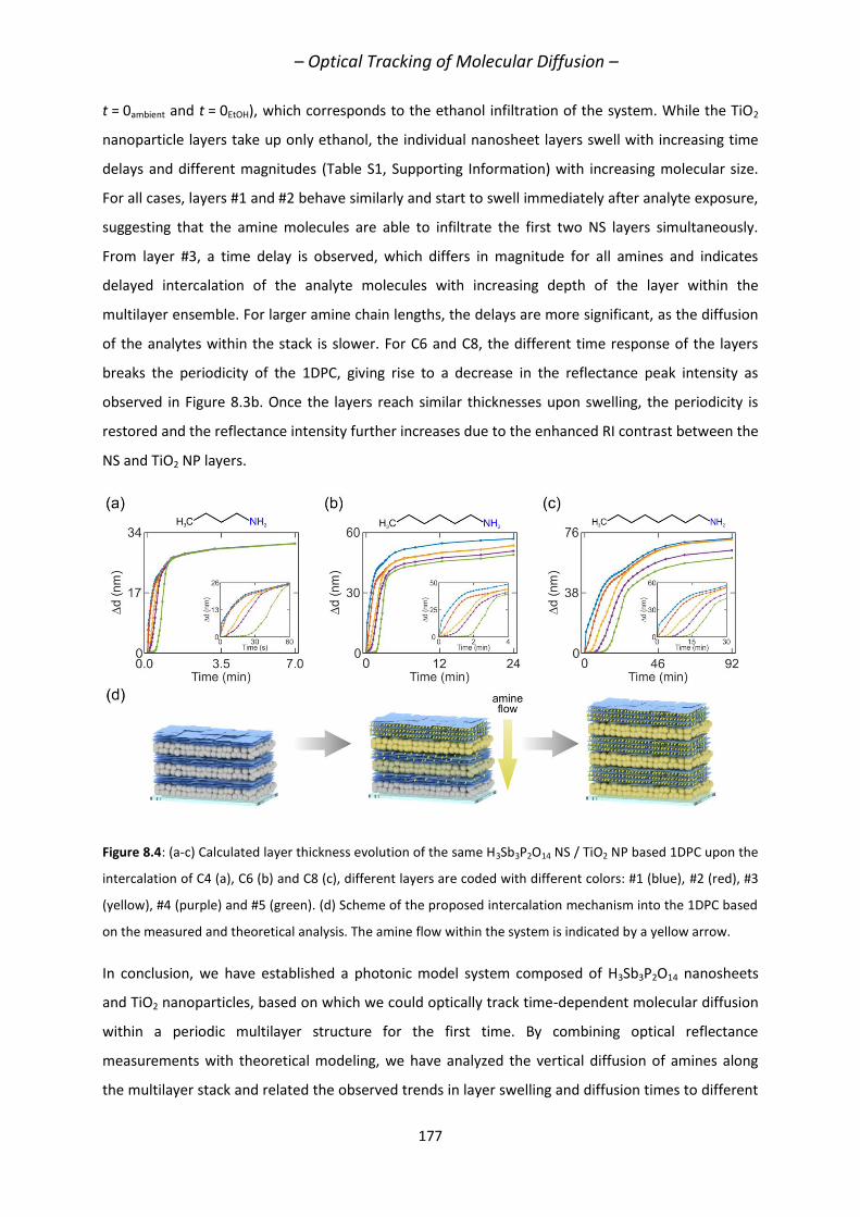
– Optical Tracking of Molecular Diffusion –
177
t = 0ambient and t = 0EtOH), which corresponds to the ethanol infiltration of the system. While the TiO2
nanoparticle layers take up only ethanol, the individual nanosheet layers swell with increasing time
delays and different magnitudes (Table S1, Supporting Information) with increasing molecular size.
For all cases, layers #1 and #2 behave similarly and start to swell immediately after analyte exposure,
suggesting that the amine molecules are able to infiltrate the first two NS layers simultaneously.
From layer #3, a time delay is observed, which differs in magnitude for all amines and indicates
delayed intercalation of the analyte molecules with increasing depth of the layer within the
multilayer ensemble. For larger amine chain lengths, the delays are more significant, as the diffusion
of the analytes within the stack is slower. For C6 and C8, the different time response of the layers
breaks the periodicity of the 1DPC, giving rise to a decrease in the reflectance peak intensity as
observed in Figure 8.3b. Once the layers reach similar thicknesses upon swelling, the periodicity is
restored and the reflectance intensity further increases due to the enhanced RI contrast between the
NS and TiO2 NP layers.
Figure 8.4: (a-c) Calculated layer thickness evolution of the same H3Sb3P2O14 NS / TiO2 NP based 1DPC upon the
intercalation of C4 (a), C6 (b) and C8 (c), different layers are coded with different colors: #1 (blue), #2 (red), #3
(yellow), #4 (purple) and #5 (green). (d) Scheme of the proposed intercalation mechanism into the 1DPC based
on the measured and theoretical analysis. The amine flow within the system is indicated by a yellow arrow.
In conclusion, we have established a photonic model system composed of H3Sb3P2O14 nanosheets
and TiO2 nanoparticles, based on which we could optically track time-dependent molecular diffusion
within a periodic multilayer structure for the first time. By combining optical reflectance
measurements with theoretical modeling, we have analyzed the vertical diffusion of amines along
the multilayer stack and related the observed trends in layer swelling and diffusion times to different
– Optical Tracking of Molecular Diffusion –
178
host-guest interactions for the different primary amines under study. With increasing molecular size,
the diffusion kinetics is significantly slowed down and the analyte reaches the layers buried beneath
the surface with a longer time delay compared to the smaller amines. Importantly, we verified that
multilayer filling is complete in all cases, but only after allowing for sufficiently long analyte diffusion
times of up to 92 min for the largest analyte octylamine, an issue that is highly relevant for correct
sensor handling. Thus, these studies do not only contribute to a better understanding of analyte
diffusion through multilayer systems, but they also reveal and rationalize key characteristics of vapor
sensors such as response and saturation times, and give insights into the sensing mechanism which is
governed by molecular properties and the strength of host-guest interactions. Ultimately, the
strategy laid out here sets the stage to study molecular diffusion processes in arbitrary photonic
structures and thin film architectures in real time, based on a simple optical read-out.
8.6 ACKNOWLEDGEMENTS
Financial support was granted by the Max Planck Society, the University of Munich (LMU), the Center
for NanoScience (CeNS), and the Deutsche Forschungsgemeinschaft (DFG) through the Cluster of
Excellence Nanosystems Initiative Munich (NIM).The authors thank for Viola Duppel for the SEM
cross section measurements. A.J.-S. gratefully acknowledges a postdoctoral scholarship from the Max
Planck Society.
8.7 REFERENCES
[1] L. Atzori, A. Iera, G. Morabito, Comput. Networks 2010, 54, 2787-2805.
[2] R. A. Potyrailo, Chem. Soc. Rev. 2017, 46, 5311-5346.
[3] V. Haasz, K. Madani, Advanced Data Acquisition and Intelligent Data Processing, River
Publishers, 2014.
[4] M. M. Cruz-Cunha, Handbook of Research on Mobility and Computing: Evolving Technologies
and Ubiquitous Impacts: Evolving Technologies and Ubiquitous Impacts, Information Science
Reference, 2011.
[5] S. Yang, C. Jiang, S.-h. Wei, Appl. Phys. Rev. 2017, 4, 021304.
[6] A. M. Azad, S. A. Akbar, S. G. Mhaisalkar, L. D. Birkefeld, K. S. Goto, J. Electrochem. Soc. 1992,
139, 3690-3704.
[7] R. Sriram, J. E. Baker, P. M. Fauchet, B. L. Miller, Proc. SPIE Vol. 8570, 2013, pp. 857007.
[8] K. Szendrei, P. Ganter, O. Sánchez-Sobrado, R. Eger, A. Kuhn, B. V. Lotsch, Adv. Mater. 2015,
27, 6341-6348.
[9] P. Ganter, K. Szendrei, B. V. Lotsch, Adv. Mater. 2016, 28, 7294-7294.
– Optical Tracking of Molecular Diffusion –
179
[10] C. Fenzl, T. Hirsch, O. S. Wolfbeis, Angew. Chem. Int. Ed. 2014, 53, 3318-3335.
[11] R. V. Nair, R. Vijaya, Prog. Quantum Electron. 2010, 34, 89-134.
[12] S. Y. Choi, M. Mamak, G. von Freymann, N. Chopra, G. A. Ozin, Nano Lett. 2006, 6, 2456.
[13] S. Colodrero, M. Ocaña, H. Míguez, Langmuir 2008, 24, 4430-4434.
[14] M. C. Fuertes, S. Colodrero, G. Lozano, A. R. González-Elipe, D. Grosso, C. Boissière, C.
Sánchez, G. J. d. A. A. Soler-Illia, H. Míguez, J. Phys. Chem. C 2008, 112, 3157-3163.
[15] M. E. Calvo, O. Sánchez-Sobrado, S. Colodrero, H. Míguez, Langmuir 2009, 25, 2443-2448.
[16] S. Colodrero, M. Ocana, A. R. Gonzalez-Elipe, H. Miguez, Langmuir 2008, 24, 9135-9139.
[17] F. M. Hinterholzinger, A. Ranft, J. M. Feckl, B. Ruhle, T. Bein, B. V. Lotsch, J. Mater. Chem.
2012, 22, 10356-10362.
[18] A. Ranft, I. Pavlichenko, K. Szendrei, P. M. Zehetmaier, Y. Hu, A. von Mankowski, B. V. Lotsch,
Microporous Mesoporous Mater. 2015, 216, 216-224.
[19] A. von Mankowski, K. Szendrei-Temesi, C. Koschnick, B. V. Lotsch, Nanoscale Hori. 2018.
[20] K. Szendrei‐Temesi, O. Sanchez‐Sobrado, S. B. Betzler, K. M. Durner, T. Holzmann, B. V.
Lotsch, Adv. Func. Mater. 2018, 28, 1705740.
[21] B. V. Lotsch, G. A. Ozin, J. Am. Chem. Soc. 2008, 130, 15252-15253.
[22] B. V. Lotsch, G. A. Ozin, Adv. Mater. 2008, 20, 4079-4084.
[23] J. Han, Y. Dou, M. Wei, D. G. Evans, X. Duan, RSC Adv. 2012, 2, 10488-10491.
[24] Z. Wang, J. Zhang, J. Xie, C. Li, Y. Li, S. Liang, Z. Tian, T. Wang, H. Zhang, H. Li, W. Xu, B. Yang,
Adv. Funct. Mater. 2010, 20, 3784-3790.
[25] P. Lova, G. Manfredi, L. Boarino, A. Comite, M. Laus, M. Patrini, F. Marabelli, C. Soci, D.
Comoretto, ACS Photonics 2015, 2, 537-543.
[26] M. E. Calvo, H. Míguez, Chem. Mater. 2010, 22, 3909-3915.
[27] M. E. Calvo, J. R. Castro Smirnov, H. Míguez, J. Polym. Sci. Part B: Polym. Phys. 2012, 50,
945-956.
[28] F. Scotognella, D. P. Puzzo, A. Monguzzi, D. S. Wiersma, D. Maschke, R. Tubino, G. A. Ozin,
Small 2009, 5, 2048-2052.
[29] A. Jiménez‐Solano, J. F. Galisteo‐López, H. Míguez, Adv. Opt. Mater. 2018, 6, 1700560.
[30] K. Szendrei, A. Jiménez-Solano, G. Lozano, B. V. Lotsch, H. Míguez, Adv. Opt. Mater. 2017, 5,
1700663.
[31] A. Ranft, F. Niekiel, I. Pavlichenko, N. Stock, B. V. Lotsch, Chem. Mater. 2015, 27, 1961–1970.
[32] Y. Kang, J. J. Walish, T. Gorishnyy, E. L. Thomas, Nat. Mater. 2007, 6, 957-960.
[33] K. Szendrei-Temesi, O. Sanchez-Sobrado, S. B. Betzler, K. M. Durner, T. Holzmann, B. V.
Lotsch, Adv. Funct. Mater., 1705740.
– Optical Tracking of Molecular Diffusion –
180
[34] A. T. Exner, I. Pavlichenko, B. V. Lotsch, G. Scarpa, P. Lugli, ACS Appl. Mater. Interfaces 2013,
5, 1575-1582.
[35] I. Pavlichenko, E. Broda, Y. Fukuda, K. Szendrei, A. K. Hatz, G. Scarpa, P. Lugli, C. Brauchle, B.
V. Lotsch, Mater. Horiz. 2015, 2, 299-308.
[36] K. P. Raymond, I. B. Burgess, M. H. Kinney, M. Loncar, J. Aizenberg, Lab Chip 2012, 12, 3666.
[37] P. Allcock, P. A. Snow, J. Appl. Phys. 2001, 90, 5052-5057.
[38] P. A. Snow, E. K. Squire, P. S. J. Russell, L. T. Canham, J. Appl. Phys. 1999, 86, 1781-1784.
[39] T. L. Kelly, A. Garcia Sega, M. J. Sailor, Nano Lett. 2011, 11, 3169-3173.
[40] C. M. Thompson, A. M. Ruminski, A. Garcia Sega, M. J. Sailor, G. M. Miskelly, Langmuir 2011,
27, 8967-8973.
[41] L. De Stefano, L. Moretti, I. Rendina, A. M. Rossi, Sens. Actuators, B 2004, 100, 168-172.
[42] J.-C. P. Gabriel, F. Camerel, B. J. Lemalre, H. Desvaux, P. Davidson, P. Batail, Nature 2001, 413,
504.
[43] Y. Piffard, A. Verbaere, A. Lachgar, S. Deniard-Courant, M. Tournoux, Rev. Chim. Miner. 1986,
23, 766-775.
[44] J. D. Joannopoulos, S. G. Johnson, J. N. Winn, R. D. Meade, Photonic crystals: molding the
flow of light, Princeton university press, 2011.
[45] L. D. Bonifacio, B. V. Lotsch, D. P. Puzzo, F. Scotognella, G. A. Ozin, Adv. Mater. 2009, 21,
1641.
[46] P. Ganter, L. M. Schoop, M. Däntl, B. V. Lotsch, Chem. Mater. 2018,
DOI:10.1021/acs.chemmater.7b04828.
[47] F. Geng, R. Ma, A. Nakamura, K. Akatsuka, Y. Ebina, Y. Yamauchi, N. Miyamoto, Y. Tateyama,
T. Sasaki, Nat. Commun. 2013, 4, 2641.
[48] F. Menendez, A. Espina, C. Trobajo, J. Rodriguez, Mater. Res. Bull. 1990, 25, 1531-1539.
[49] P. Yeh, Optical Waves in Layered Media, John Wiley & Sons, New York, 1988.
[50] E. Hecht, Optics, Addison-Wesley, Reading, Mass., 2002.
[51] D. E. Goldberg, Genetic Algorithms in Search, Optimization and Machine Learning, Addison-
Wesley Longman Publishing Co., Inc., 1989.
[52] M. E. Calvo, L. González-García, J. Parra-Barranco, A. Barranco, A. Jiménez-Solano, A. R.
González-Elipe, H. Míguez, Adv. Opt. Mater. 2015, 3, 171-175.
[53] A. Garahan, L. Pilon, J. Yin, I. Saxena, J. Appl. Phys. 2007, 101, 014320.
[54] N. Nagy, Deak, A., Horvölgyi, Z., Fried, M., Agod, A., Barsony, I., Langmuir 2006, 26, 8416-
8423.
– Conclusion and Outlook –
181
9. CONCLUSION AND OUTLOOK
This thesis addresses current challenges in the evermore developing research field of sensing, which
are particularly valid for optical sensing schemes. Here, we suggested new material-based solutions
to key sensing characteristics, namely improved selectivity, sensitivity, sensor stability, alternative
readout schemes, fast response times and high reversibility. An important motivation of this thesis is
to create material-based sensors with inherently robust inorganic materials, which are nanosized,
chemically tailorable and solution-processable. Due to the large chemical variety and the possibility
for chemical modifications, 2D nanosheet materials carry an inherent potential for resolving the
above issues and offer new perspectives in terms of miniaturization and versatility. 2D nanosheet
materials were thus chosen as nanosized functional building blocks and were integrated into a simple
optical sensing architecture with well-defined optical properties – 1-dimensional Photonic Crystals.
The first approach aiming at an increase of the sensitivity utilizes swellable antimony phosphate
nanosheets, H3Sb3P2O14, as stimuli-responsive materials in 1DPC architectures. These show a
pronounced layer thickness increase in response to changes of environmental humidity (Chapter 3).
Due to the highly porous character of the multilayer system and the inherently fast response time of
the nanosheets, the water uptake process is rapid, which lead to the realization of novel humidity
sensing based applications. By realizing optical touchless finger motion tracking, we showed that
these ultrasensitive humidity sensors are capable of tracking the humid atmosphere of a human
finger under touchless conditions in real-time and true color. Further, several real-world sensor
applications were studied, such as the temperature dependency, the cyclability, the reproducibility of
the sensing event and the cross sensitivity to other volatile analytes (Chapter 4).
In a second approach aiming to increase the selectivity of these platforms, we integrated HSbP2O8 as
another member of the antimony phosphate family into 1DPCs. These nanosheets proved
themselves as a smart functional building block with an inherent capability to differentiate various
volatile organic analytes (Chapter 5). By using a single-component sensor and without any statistical
analysis, the response time and the stopband shifts were combined and utilized as useful sensing
– Conclusion and Outlook –
182
descriptors. Based on these two descriptors, we were able to show the potential of this platform to
optically differentiate between volatile organic compounds, besides the ultrahigh sensitivity for
water vapor. Moreover, different alcohols (i.e. methanol and ethanol) and even constitutional
isomers (i.e. 2-butanol and 1-butanol) could be distinguished by our sensor, which are usually
difficult to differentiate by optical readout techniques.
Further, to optimize the optical properties of 1DPC based sensing devices, the optical contrast
between the two constituent materials of the multilayer system were enhanced by applying the
ultrahigh refractive index nanosheet material lithium tin sulfide (Chapter 6). With this approach, we
could reduce the number of layers that form the structure, leading to a thickness reduction of about
60%, which could result in a significant decrease of production time and cost whilst maintaining the
excellent optical properties, such as the high reflectance and the high humidity sensitivity. We could
even further increase the humidity sensitivity by combining two swelling nanosheet materials - high
RI lithium tin sulfide nanosheets and the previously introduced antimony phosphate nanosheets.
Not only the stimuli-responsive materials in 1DPCs were developed, but also the sensor
architectures: we integrated the swelling nanosheets into carefully designed optical resonator
structures (Chapter 7). Hereby, we utilized the coupling of photoluminescence of nanoemitters with
the photonic modes sustained by the structure. To this end, we embedded into rationally designed
photonic resonator structures a thin layer of dye-functionalized nanospheres into the
humidity-responsive defect layer at a well-defined position. By dynamic humidity induced changes of
the optical cavity composed of swellable antimony phosphate nanosheets, changes in the
photoluminescence could be induced, which lead to the creation of the first luminescent photonic
humidity sensor. Furthermore, complete suppression of the photoluminescence at a certain humidity
level was demonstrated, which allowed to construct humidity driven luminescent switches.
Finally, we investigated important features regarding time-dependent sensing mechanisms and the
analyte infiltration into the multilayered structure (Chapter 8). For this, a model system was
constructed, a H3Sb3P2O14 nanosheet / TiO2 nanoparticle based 1DPC, which is capable of
intercalating (primary) amines due to the formation of ammonium ions in the interlayer space. By
varying the amine chain length, the response time and the stopband shift can be dynamically tuned
and different sensor-analyte interactions can be obtained. Additionally, extensive theoretical
investigations were performed, whereby the exact layer thicknesses of the 1DPCs depending on the
progress of the chemical diffusion were extracted by fitting the time-dependent reflectance
measurements. As a result, we can temporally resolve the vertical analyte infiltration into the
multilayer, relying on optical methods.
– Conclusion and Outlook –
183
In conclusion, novel material-based solutions were proposed which address key challenges in the
design of optical vapor sensors, such as the selectivity, sensitivity, optical properties and readout
schemes. However, for the applicability and the integration of such 1DPC-based functional material
based sensors into devices, some remaining challenges are to be solved.
9.1 OUTLOOK
Although these material-based solutions offer enhancement in the sensing performance, for an
integration of these optical sensors into sensing devices some general issues and case- and
application-specific problems are to be overcome. In the following, some of these issues are
discussed.
Tuning the Sensitivity Towards Other Analytes
In this thesis, mostly optical sensors were presented where the sensitivity towards water vapor is
decisive. Even for the volatile organic compound (VOC) sensors (Chapter 5), the humidity sensitivity
was the primary effect. For environmental or industrial applications, diverse target vapors and gases
are relevant, e.g. toxic gases, such as CO2, CO, NOx or SO2,[1, 2] or acetone and ethanol for medical
diagnostic approaches or breathalyzers. For these approaches it is also crucial that the sensing
response is independent of the ambient conditions, such as the temperature or the relative humidity,
e.g. there is no cross-sensitivity of the sensor towards water vapor. These goals may be solved with
covalent or intercalative modification[3] of the here presented 2D material based sensing devices.
This chemical modification of the nanosheets with tailor-made functional groups can lead to specific
molecular interactions and a selective adsorption of the gases or vapors.
Flexible Structures
To address diverse sensing needs and application requirements, it would be advantageous to make
such optical sensors flexible. One approach aiming a transferable and free standing 1DPCs was
presented in the literature.[4, 5] However, through the filling of the porous structure with a flexible
polymer, the porosity and with it, the sensing capability, is suppressed. For this reason, other
approaches have to be tested in order to make these sensors mechanically flexible, but keep the
vapor responsiveness, such as the usage of a flexible substrate or the transfer of the multilayer to a
flexible substrate. First preliminary results show that the nanosheets imbue the entire multilayer
structure with mechanical stability, which in extreme cases, such as under ultrahigh vacuum in the
scanning electron microscopy measurements, can lead to peeling off of the entire structure without
destroying the nanostructure (Figure 9.1).
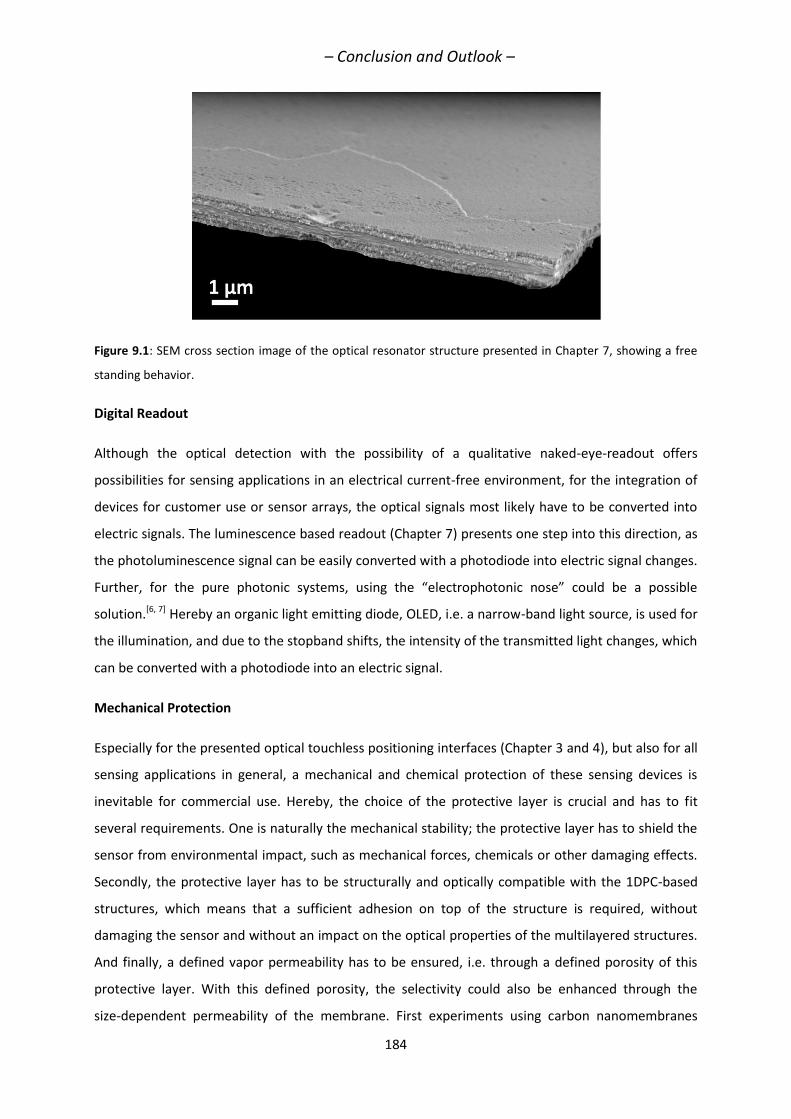
– Conclusion and Outlook –
184
Figure 9.1: SEM cross section image of the optical resonator structure presented in Chapter 7, showing a free
standing behavior.
Digital Readout
Although the optical detection with the possibility of a qualitative naked-eye-readout offers
possibilities for sensing applications in an electrical current-free environment, for the integration of
devices for customer use or sensor arrays, the optical signals most likely have to be converted into
electric signals. The luminescence based readout (Chapter 7) presents one step into this direction, as
the photoluminescence signal can be easily converted with a photodiode into electric signal changes.
Further, for the pure photonic systems, using the “electrophotonic nose” could be a possible
solution.[6, 7] Hereby an organic light emitting diode, OLED, i.e. a narrow-band light source, is used for
the illumination, and due to the stopband shifts, the intensity of the transmitted light changes, which
can be converted with a photodiode into an electric signal.
Mechanical Protection
Especially for the presented optical touchless positioning interfaces (Chapter 3 and 4), but also for all
sensing applications in general, a mechanical and chemical protection of these sensing devices is
inevitable for commercial use. Hereby, the choice of the protective layer is crucial and has to fit
several requirements. One is naturally the mechanical stability; the protective layer has to shield the
sensor from environmental impact, such as mechanical forces, chemicals or other damaging effects.
Secondly, the protective layer has to be structurally and optically compatible with the 1DPC-based
structures, which means that a sufficient adhesion on top of the structure is required, without
damaging the sensor and without an impact on the optical properties of the multilayered structures.
And finally, a defined vapor permeability has to be ensured, i.e. through a defined porosity of this
protective layer. With this defined porosity, the selectivity could also be enhanced through the
size-dependent permeability of the membrane. First experiments using carbon nanomembranes
– Conclusion and Outlook –
185
(CNM)[8, 9] confirmed the optical and structural compatibility with the 1DPCs, but further
investigations are needed in order to quantify the impact of the CNM layer on analyte diffusion.
9.2 REFERENCES
[1] A. M. Azad, S. A. Akbar, S. G. Mhaisalkar, L. D. Birkefeld, K. S. Goto, J. Electrochem. Soc. 1992,
139, 3690-3704.
[2] W. Hong, Y. Chen, X. Feng, Y. Yan, X. Hu, B. Zhao, F. Zhang, D. Zhang, Z. Xu, Y. Lai, Chem.
Commun. 2013, 49, 8229-8231.
[3] P. Ganter, L. M. Schoop, B. V. Lotsch, Adv. Mater. 2017, 29, 1604884.
[4] M. E. Calvo, H. Míguez, Chem. Mater. 2010, 22, 3909-3915.
[5] M. E. Calvo, J. R. Castro Smirnov, H. Míguez, J. Polym. Sci. Part B: Polym. Phys. 2012, 50,
945-956.
[6] A. T. Exner, I. Pavlichenko, D. Baierl, M. Schmidt, G. Derondeau, B. V. Lotsch, P. Lugli, G.
Scarpa, Laser Photonics Rev. 2014, 5, 726-733.
[7] I. Pavlichenko, E. Broda, Y. Fukuda, K. Szendrei, A. K. Hatz, G. Scarpa, P. Lugli, C. Brauchle, B.
V. Lotsch, Mater. Horiz. 2015, 2, 299-308.
[8] A. Turchanin, A. Gölzhäuser, Adv. Mater. 2016, 28, 6075-6103.
[9] P. Angelova, H. Vieker, N.-E. Weber, D. Matei, O. Reimer, I. Meier, S. Kurasch, J. Biskupek, D.
Lorbach, K. Wunderlich, L. Chen, A. Terfort, M. Klapper, K. Müllen, U. Kaiser, A. Gölzhäuser, A.
Turchanin, ACS Nano 2013, 7, 6489-6497.


– Appendix –
187
10. APPENDIX
In this section, a list of important abbreviations, the Supporting Informations for Chapter 3, Chapter
5, Chapter 6, Chapter 7 and Chapter 8 are provided, which are followed by a List of Publications and
Scientific Contributions and a short Curriculum Vitae.
10. APPENDIX 187
LIST OF ABBREVIATIONS 188
10.1 SUPPORTING INFORMATION FOR CHAPTER 3 190
10.2 SUPPORTING INFORMATION FOR CHAPTER 5 209
10.3 SUPPORTING INFORMATION FOR CHAPTER 6 226
10.4 SUPPORTING INFORMATION FOR CHAPTER 7 236
10.5 SUPPORTING INFORMATION FOR CHAPTER 8 238
10.6 LIST OF PUBLICATIONS 245
10. 7 CONTRIBUTIONS TO CONFERENCES 247
10.8 CURRICULUM VITAE 249
– Appendix –
188
LIST OF ABBREVIATIONS
1D 1-dimensional
2D 2-dimensional
3D 3-dimensional
A Absorptance
AFM Atomic Force Microscopy
BF Bright Field
BP Bragg Peak
BS Bragg Stack
CEM Controlled Evaporation Mixer
DBR Distributed Bragg reflector
DF Dark Field
DLS Dynamic Light Scattering
EDX Energy-Dispersive X-ray
EELS Electron Energy Loss Spectroscopy
EM Eletromagnetic
FIB Focused Ion Beam
GA Genetic Algorithm
I Intensity
ICP Inductively Coupled Plasma
IoT Internet of Things
LDH Layered Double Hydroxide
LFC Liquid Flow Controller
LTS Lithium Tin Sulfide
MFC Mass Flow Controller
MOF Metal-Organic Framework
NP Nanoparticle
NS Nanosheet
PC Photonic Crystal
PCA Principal Component Analysis
PL Photoluminescence
R Reflectance
RH Relative Humidity
RI Refractive Index

– Appendix –
189
SAED Selected Area Electron Diffraction
SEM Scanning Electron Microscopy
STEM Scanning Transmission Electron Microscopy
T Transmittance
TEM Transmission Electron Microscopy
TMM Transfer Matrix Method
UV Ultraviolet
Vis Visible
VOC Volatile Organic Compound
XRD X-ray Diffraction
– Appendix –
190
10.1 SUPPORTING INFORMATION FOR CHAPTER 3
Touchless Optical Finger Motion Tracking based on 2D Nanosheets with
Giant Moisture Responsiveness
Katalin Szendrei ¶, Pirmin Ganter ¶, Olalla Sànchez-Sobrado, Roland Eger, Alexander Kuhn, Bettina V.
Lotsch*
¶ These authors contributed equally to this work.
METHODS
Solid state synthesis, protonation and exfoliation of nanosheets
For the synthesis of K3Sb3P2O14 the precursors (KNO3 (99 %, Merck), Sb2O3 (99.6 %, Alfa Aesar),
NH4H2PO4 (98 %+, Acros Organics)) were thoroughly ground in a stoichiometric ratio and heated up
as described elsewhere.[1] For the proton exchange reaction, 2 g of K3Sb3P2O14 were treated with
250 mL of 8 M nitric acid (diluted 65 wt%, Merck) overnight, filtrated, washed with ethanol and dried
at room temperature. This treatment was repeated one more time to complete the exchange
reaction.[2] The success was monitored by XRD. Exfoliation was carried out by stirring the H3Sb3P2O14
vigorously overnight in pure water with a concentration of bulk protons of 7.3 mmol L-1. The
obtained colloidal suspensions were centrifuged at 3000 rpm for 30 min to remove non-exfoliated
bulk material. The supernatant is a suspension of mainly single-layer nanosheets. To obtain the
nanosheet pellet, an additional centrifugation step was applied at 18000 rpm for 30 min. The
supernatant was discarded and the gel-like colorless wet aggregate was dried at 100 °C.
Synthesis of nanoparticles
TiO2 nanoparticulate sols were synthesized using a procedure described elsewhere.[3] The colloidal
suspension of titania nanoparticles used for spin-coating was obtained by collection of the particles
by repeated centrifugation at 24000 rpm and redispersion in methanol.
SiO2 nanocolloids were purchased from Dupont (LUDOX TMA, Aldrich, 30 nm particle size, 34 wt%).
Preparation of colloidal suspensions
The dried colorless precipitate of the water exfoliated H3Sb3P2O14 nanosheets was redispersed with a
concentration of 42 mmol L-1 in a water/ethanol mixture (60 vol% ethanol) and sonicated for 2 h. The
TiO2 suspensions had a concentration of 2.5 wt% in methanol. The commercial colloids of SiO2 were
redispersed at 3 wt% in methanol.
– Appendix –
191
Fabrication of thin films and Bragg stacks
All films were made by means of spin-coating using a spin-coater (WS-650S-NPP-Lite, Laurell
Technologies Corporation) and concentrations given above. Different film thicknesses were accessed
by varying the spin-coating speed, which allowed the fine-tuning of the optical properties.[4] On
plasma cleaned microscope glass slides with the dimensions of 2.5 cm x 2.5 cm, 400 µl of the
colloidal suspensions were spin-coated alternatingly for 1 min with a defined speed, and heated to
80 °C for 15 min after each layer deposition. 2000 rpm, 3000 rpm and 4000 rpm spin-coating speeds
were applied (the same speed for each layer within a Bragg stack) to tune the optical properties,
while other parameters such as colloidal concentration, spin-coating time and acceleration rate
(10000 rpm/s) were kept constant. For conductance measurements, this redispersed Sb3P2O143-
nanosheet colloid was spin-coated at 3000 rpm or 2000 rpm for 1 min with a 10000 rpm s-1
acceleration ramp on a 1.5 cm x 1.5 cm plasma-cleaned quartz substrate. Gold contacts were sputter-
coated (108auto, Cressington) with 180 s sputtering time.
CHARACTERIZATION
Structural characterization
TEM images and selected area electron diffraction (SAD) patterns were obtained with a Phillips CM30
ST TEM (300 kV, LaB6 cathode) equipped with a Gatan CCD camera. TEM-EDX analysis was performed
with a Si/Li detector (Thermo Fisher, Noran System Seven). SEM images of the nanosheet pellet were
collected with a Vega TS 5130 MM (Tescan) equipped with Si/Li detector (Oxford). SEM cross-
sectional images of the Bragg stacks were taken with a Zeiss Merlin FE-SEM. AFM measurements
were done on a Veeco CP II system in non-contact mode. XRD patterns were collected on a powder
X-ray diffractometer (Stadi P, STOE) working with Ge(111) monochromated Mo-K1 radiation
(λ = 70.926 pm) or Cu-K1 radiation (λ = 154.051 pm) in Debye-Scherrer or transmission geometry
with an image-plate detector or a point detector. Well-ground samples were either put between two
Mylar® foils or filled in a glass capillary. Indexing was performed with the software DiffracPlus TOPAS
v4.2 (Bruker AXS). The images of the Bragg stack surfaces were obtained with an optical microscope
(Olympus BX51), operating in reflection mode with a 4x objective.
Conductance measurements
To obtain the conductance measurements, two different methodologies were used. In the first one,
the films were kept over saturated salt solutions,[5, 6] at around 25 °C in a closed atmosphere at least
15 min before the conductance measurements. In the second one, we used an argon flow set up
(Figure S 3.10). A dry Ar flow and a water vapor saturated Ar stream were mixed in different ratios to
– Appendix –
192
define the humidity between 0-93.5%. The setup was calibrated using the conductance values
previously measured at the RH defined by the salt solutions. The cycling experiments were
performed with either the Ar flow setup, Figure S 3.10, or by a tapping motion of a human finger. The
change in conductance was monitored by impedance spectroscopy (in plane geometry, two point
measurement) with an impedance bridge (Princeton Apllied Research, VersaSTAT MC) applying an AC
voltage of 500 mV and a frequency range of 1 Hz to 1 MHz. Cycling measurements were performed
with a fixed frequency of 300 Hz.
Optical measurements
Porosimetry measurements were carried out by the porosimetry tool of Sopra PS-1000 SAM,
whereby the sample was equilibrated at all water vapor relative pressure values for 15 min. The
measurement results were fitted with the software Sopra SAE using the model combination Cauchy
and Lorentz. The thickness of the nanoparticle layers was considered as constant and only the
refractive index was fitted over the relative pressure range. For the nanosheet thin films both values,
the layer thickness and also the refractive index were fitted. Before all measurements, the
nanoparticle samples were heated for at least 30 min at 200 °C and the nanosheet thin films for 30
min at 60 °C in vacuum to make sure that the pores are empty. To obtain the optical isotherms, all
fitted measurement results were plotted against the analyte relative pressure.
All optical spectra were measured with a fiber optic spectrometer (USB2000+, Ocean Optics)
attached to a microscope (DM2500, Leica) with normal incidence and the optical spectra were always
taken at the same spot (1×1 mm2 in area). To obtain the optical changes with relative humidity
change, the Bragg stacks were kept in a stainless steel chamber with a transparent glass window and
a total volume of 5 mL, placed above 0.7 mL of the saturated salt solutions at around 25 °C[5,6] as
described above (see conductance measurements). At each step, 20 min atmosphere equilibration
time was needed. To illustrate the reversibility, a dynamic method using a nitrogen flow setup (see
below) was applied. Hereby, the reflectance intensity changes of the Bragg peak were observed at a
certain wavelength placed at the red stop band edge. While the Bragg peak shifts in response to the
analyte exposure, the reflectance intensity changes at the observed wavelength. In these dynamic
measurements, the BSs were placed into a closed chamber with the dimensions of
2.5 x 2.5 x 0.5 cm3, where well-defined relative humidity values were realized by connecting the
inserted pipette tip with a liquid-gas flow controller (Bronkhorst) and a vaporizer (CEM) with a
massflow-controlled carrier gas flow. To observe a specific relative humidity, the carrier gas nitrogen
(200 mL min-1) and the liquid water were dosed into the CEM (controlled evaporation and mixing,
W101A-130-K, Bronkhorst High-Tech),[7] where the thermal evaporation of water took place. The
CEM was heated to temperatures above the boiling point (120 °C for water). The relative vapor
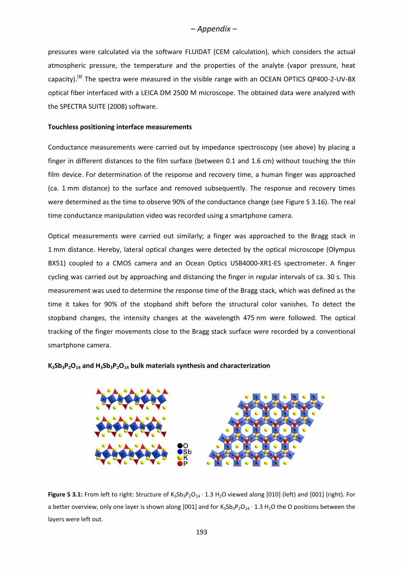
– Appendix –
193
pressures were calculated via the software FLUIDAT (CEM calculation), which considers the actual
atmospheric pressure, the temperature and the properties of the analyte (vapor pressure, heat
capacity).[8] The spectra were measured in the visible range with an OCEAN OPTICS QP400-2-UV-BX
optical fiber interfaced with a LEICA DM 2500 M microscope. The obtained data were analyzed with
the SPECTRA SUITE (2008) software.
Touchless positioning interface measurements
Conductance measurements were carried out by impedance spectroscopy (see above) by placing a
finger in different distances to the film surface (between 0.1 and 1.6 cm) without touching the thin
film device. For determination of the response and recovery time, a human finger was approached
(ca. 1 mm distance) to the surface and removed subsequently. The response and recovery times
were determined as the time to observe 90% of the conductance change (see Figure S 3.16). The real
time conductance manipulation video was recorded using a smartphone camera.
Optical measurements were carried out similarly; a finger was approached to the Bragg stack in
1 mm distance. Hereby, lateral optical changes were detected by the optical microscope (Olympus
BX51) coupled to a CMOS camera and an Ocean Optics USB4000-XR1-ES spectrometer. A finger
cycling was carried out by approaching and distancing the finger in regular intervals of ca. 30 s. This
measurement was used to determine the response time of the Bragg stack, which was defined as the
time it takes for 90% of the stopband shift before the structural color vanishes. To detect the
stopband changes, the intensity changes at the wavelength 475 nm were followed. The optical
tracking of the finger movements close to the Bragg stack surface were recorded by a conventional
smartphone camera.
K3Sb3P2O14 and H3Sb3P2O14 bulk materials synthesis and characterization
Figure S 3.1: From left to right: Structure of K3Sb3P2O14 ∙ 1.3 H2O viewed along [010] (left) and [001] (right). For
a better overview, only one layer is shown along [001] and for K3Sb3P2O14 ∙ 1.3 H2O the O positions between the
layers were left out.
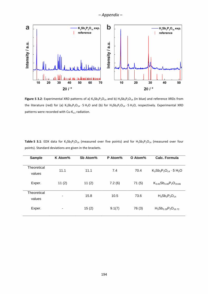
– Appendix –
194
Figure S 3.2: Experimental XRD patterns of a) K3Sb3P2O14 and b) H3Sb3P2O14 (in blue) and reference XRDs from
the literature (red) for (a) K3Sb3P2O14 ∙ 5 H2O and (b) for H3Sb3P2O14 ∙ 5 H2O, respectively. Experimental XRD
patterns were recorded with Cu-K1 radiation.
Table S 3.1: EDX data for K3Sb3P2O14 (measured over five points) and for H3Sb3P2O14 (measured over four
points). Standard deviations are given in the brackets.
Sample K Atom% Sb Atom% P Atom% O Atom% Calc. Formula
Theoretical
values 11.1 11.1 7.4 70.4 K3Sb3P2O14 ∙ 5 H2O
Exper. 11 (2) 11 (2) 7.2 (6) 71 (5) K3.05Sb3.08P2O19.86
Theoretical
values - 15.8 10.5 73.6 H3Sb3P2O14
Exper. - 15 (2) 9.1(7) 76 (3) H3Sb3.28P2O16.72
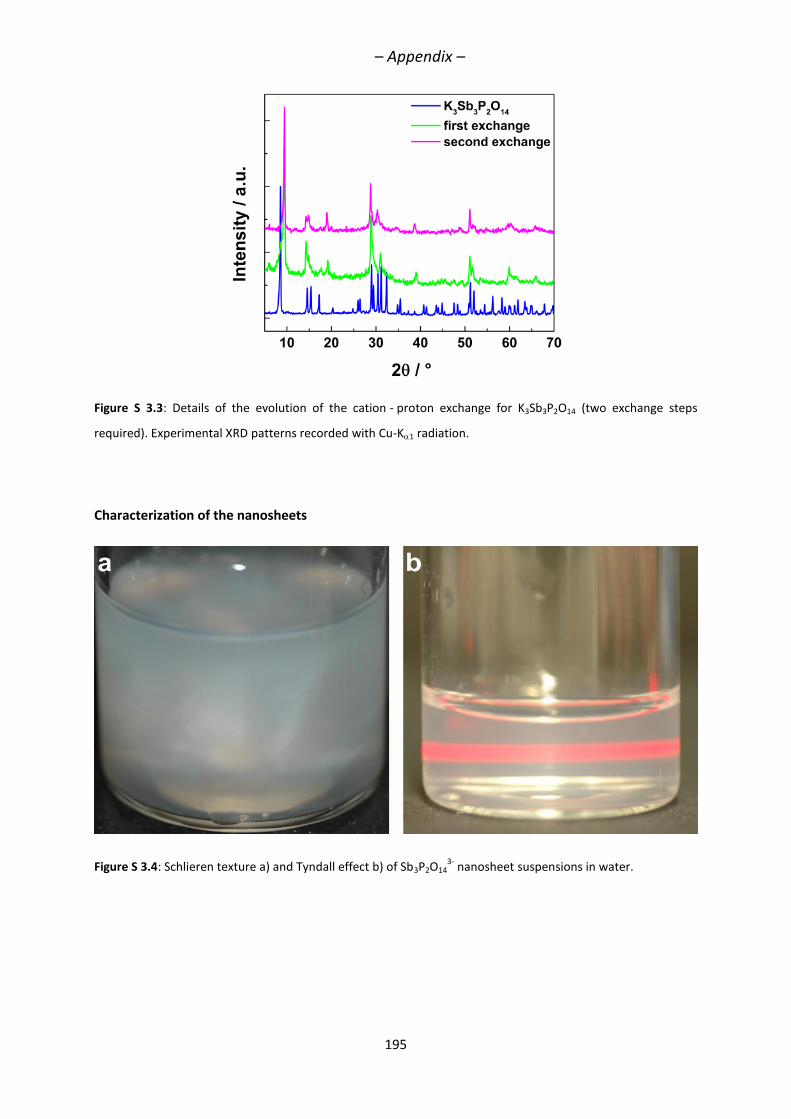
– Appendix –
195
Figure S 3.3: Details of the evolution of the cation - proton exchange for K3Sb3P2O14 (two exchange steps
required). Experimental XRD patterns recorded with Cu-K1 radiation.
Characterization of the nanosheets
Figure S 3.4: Schlieren texture a) and Tyndall effect b) of Sb3P2O143-
nanosheet suspensions in water.
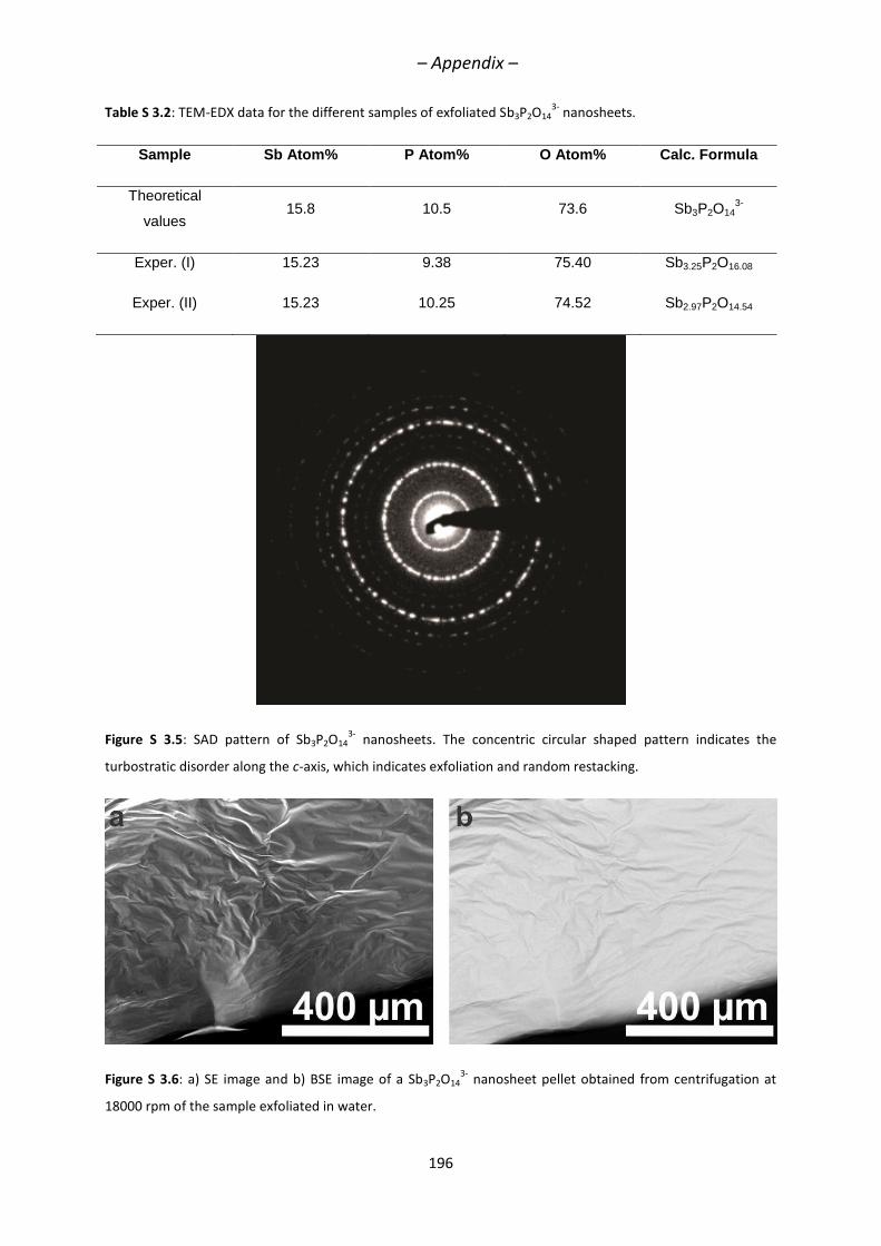
– Appendix –
196
Table S 3.2: TEM-EDX data for the different samples of exfoliated Sb3P2O143-
nanosheets.
Sample Sb Atom% P Atom% O Atom% Calc. Formula
Theoretical
values 15.8 10.5 73.6 Sb3P2O14
3-
Exper. (I) 15.23 9.38 75.40 Sb3.25P2O16.08
Exper. (II) 15.23 10.25 74.52 Sb2.97P2O14.54
Figure S 3.5: SAD pattern of Sb3P2O143-
nanosheets. The concentric circular shaped pattern indicates the
turbostratic disorder along the c-axis, which indicates exfoliation and random restacking.
Figure S 3.6: a) SE image and b) BSE image of a Sb3P2O143-
nanosheet pellet obtained from centrifugation at
18000 rpm of the sample exfoliated in water.

– Appendix –
197
Table S 3.3: SEM-EDX analysis of a Sb3P2O143-
nanosheet pellet obtained from three sample points.
Sample Sb Atom% P Atom% O Atom% Calc. Formula
Theoretical
values 15.8 10.5 73.6 Sb3P2O14
3-
Exper. 13.0 (5) 8.4 (2) 78.6 (7) Sb3.10P2O18.71
Table S 3.4: Comparison and indexing of d-values of SAD and XRD pattern (Figure S 3.7). The value marked with
an asterisk cannot clearly be determined because of a broad maximum only slightly above the noise level in the
XRD pattern.
Sb3P2O143-
Miller indices
d-value SAD
[Å]
d value XRD
[Å]
(10) 6.02 6.12
(11) 3.55 3.41*
(20) 3.04 3.06
(21) 2.34 2.32
(30) 2.04 2.04
(22) 1.77 1.77
(40) 1.53 1.53
(23) 1.41 1.41
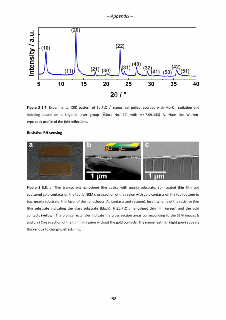
– Appendix –
198
Figure S 3.7: Experimental XRD pattern of Sb3P2O143-
nanosheet pellet recorded with Mo-Kα1 radiation and
indexing based on a trigonal layer group (p3m1 No. 72) with a = 7.0914(3) Å. Note the Warren-
type peak profile of the (hk) reflections.
Resistive RH sensing
Figure S 3.8: a) Thin transparent nanosheet film device with quartz substrate, spin-coated thin film and
sputtered gold contacts on the top. b) SEM cross-section of the region with gold contacts on the top (bottom to
top: quartz substrate, thin layer of the nanosheets, Au contacts and vacuum). Inset: scheme of the resistive thin
film substrate indicating the glass substrate (black), H3Sb3P2O14 nanosheet thin film (green) and the gold
contacts (yellow). The orange rectangles indicate the cross section areas corresponding to the SEM images b
and c. c) Cross-section of the thin film region without the gold contacts. The nanosheet film (light grey) appears
thicker due to charging effects in c.
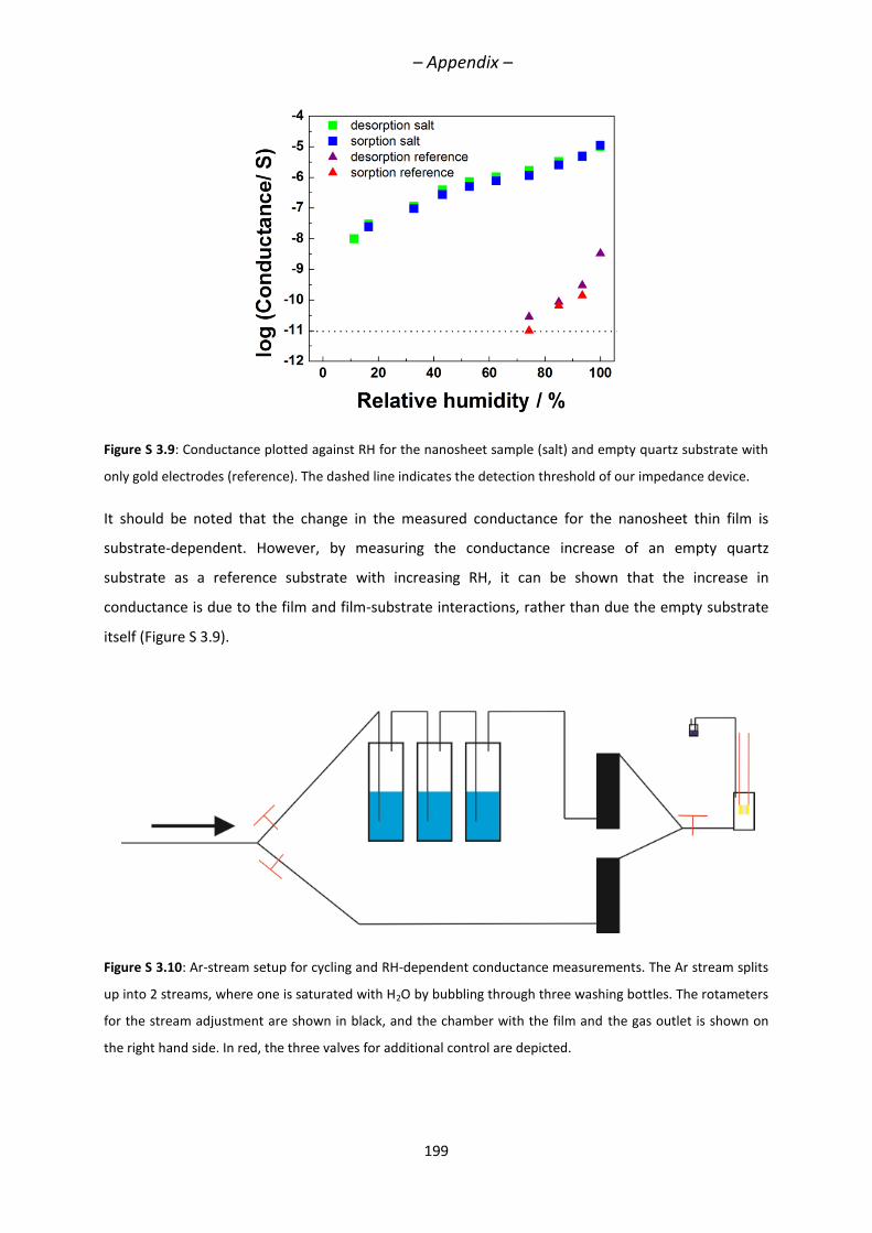
– Appendix –
199
Figure S 3.9: Conductance plotted against RH for the nanosheet sample (salt) and empty quartz substrate with
only gold electrodes (reference). The dashed line indicates the detection threshold of our impedance device.
It should be noted that the change in the measured conductance for the nanosheet thin film is
substrate-dependent. However, by measuring the conductance increase of an empty quartz
substrate as a reference substrate with increasing RH, it can be shown that the increase in
conductance is due to the film and film-substrate interactions, rather than due the empty substrate
itself (Figure S 3.9).
Figure S 3.10: Ar-stream setup for cycling and RH-dependent conductance measurements. The Ar stream splits
up into 2 streams, where one is saturated with H2O by bubbling through three washing bottles. The rotameters
for the stream adjustment are shown in black, and the chamber with the film and the gas outlet is shown on
the right hand side. In red, the three valves for additional control are depicted.
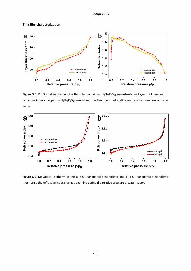
– Appendix –
200
Thin film characterization
Figure S 3.11: Optical isotherms of a thin film containing H3Sb3P2O14 nanosheets. a) Layer thickness and b)
refractive index change of a H3Sb3P2O14 nanosheet thin film measured at different relative pressures of water
vapor.
Figure S 3.12: Optical isotherm of the a) SiO2 nanoparticle monolayer and b) TiO2 nanoparticle monolayer
monitoring the refractive index changes upon increasing the relative pressure of water vapor.
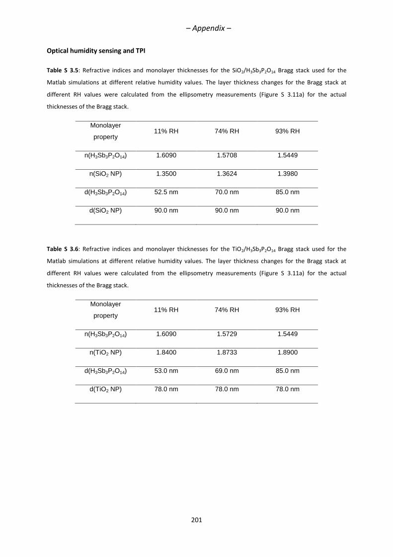
– Appendix –
201
Optical humidity sensing and TPI
Table S 3.5: Refractive indices and monolayer thicknesses for the SiO2/H3Sb3P2O14 Bragg stack used for the
Matlab simulations at different relative humidity values. The layer thickness changes for the Bragg stack at
different RH values were calculated from the ellipsometry measurements (Figure S 3.11a) for the actual
thicknesses of the Bragg stack.
Monolayer
property 11% RH 74% RH 93% RH
n(H3Sb3P2O14) 1.6090 1.5708 1.5449
n(SiO2 NP) 1.3500 1.3624 1.3980
d(H3Sb3P2O14) 52.5 nm 70.0 nm 85.0 nm
d(SiO2 NP) 90.0 nm 90.0 nm 90.0 nm
Table S 3.6: Refractive indices and monolayer thicknesses for the TiO2/H3Sb3P2O14 Bragg stack used for the
Matlab simulations at different relative humidity values. The layer thickness changes for the Bragg stack at
different RH values were calculated from the ellipsometry measurements (Figure S 3.11a) for the actual
thicknesses of the Bragg stack.
Monolayer
property 11% RH 74% RH 93% RH
n(H3Sb3P2O14) 1.6090 1.5729 1.5449
n(TiO2 NP) 1.8400 1.8733 1.8900
d(H3Sb3P2O14) 53.0 nm 69.0 nm 85.0 nm
d(TiO2 NP) 78.0 nm 78.0 nm 78.0 nm
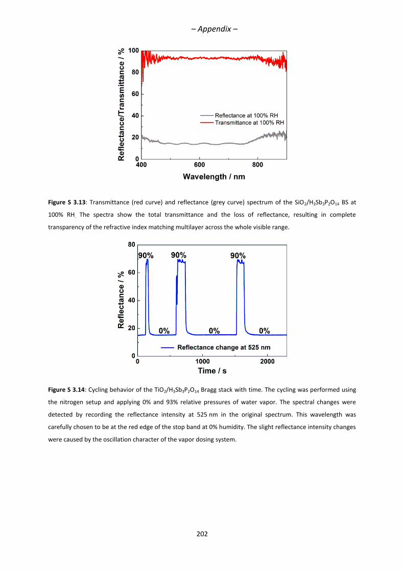
– Appendix –
202
Figure S 3.13: Transmittance (red curve) and reflectance (grey curve) spectrum of the SiO2/H3Sb3P2O14 BS at
100% RH. The spectra show the total transmittance and the loss of reflectance, resulting in complete
transparency of the refractive index matching multilayer across the whole visible range.
Figure S 3.14: Cycling behavior of the TiO2/H3Sb3P2O14 Bragg stack with time. The cycling was performed using
the nitrogen setup and applying 0% and 93% relative pressures of water vapor. The spectral changes were
detected by recording the reflectance intensity at 525 nm in the original spectrum. This wavelength was
carefully chosen to be at the red edge of the stop band at 0% humidity. The slight reflectance intensity changes
were caused by the oscillation character of the vapor dosing system.
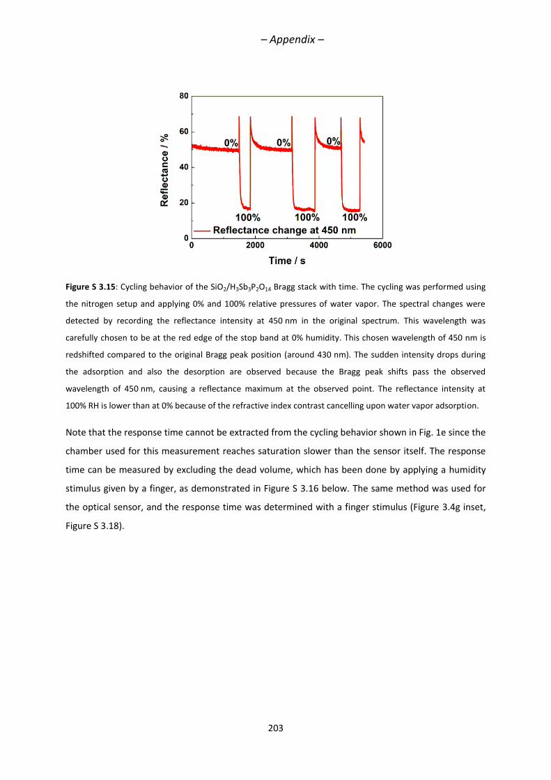
– Appendix –
203
Figure S 3.15: Cycling behavior of the SiO2/H3Sb3P2O14 Bragg stack with time. The cycling was performed using
the nitrogen setup and applying 0% and 100% relative pressures of water vapor. The spectral changes were
detected by recording the reflectance intensity at 450 nm in the original spectrum. This wavelength was
carefully chosen to be at the red edge of the stop band at 0% humidity. This chosen wavelength of 450 nm is
redshifted compared to the original Bragg peak position (around 430 nm). The sudden intensity drops during
the adsorption and also the desorption are observed because the Bragg peak shifts pass the observed
wavelength of 450 nm, causing a reflectance maximum at the observed point. The reflectance intensity at
100% RH is lower than at 0% because of the refractive index contrast cancelling upon water vapor adsorption.
Note that the response time cannot be extracted from the cycling behavior shown in Fig. 1e since the
chamber used for this measurement reaches saturation slower than the sensor itself. The response
time can be measured by excluding the dead volume, which has been done by applying a humidity
stimulus given by a finger, as demonstrated in Figure S 3.16 below. The same method was used for
the optical sensor, and the response time was determined with a finger stimulus (Figure 3.4g inset,
Figure S 3.18).
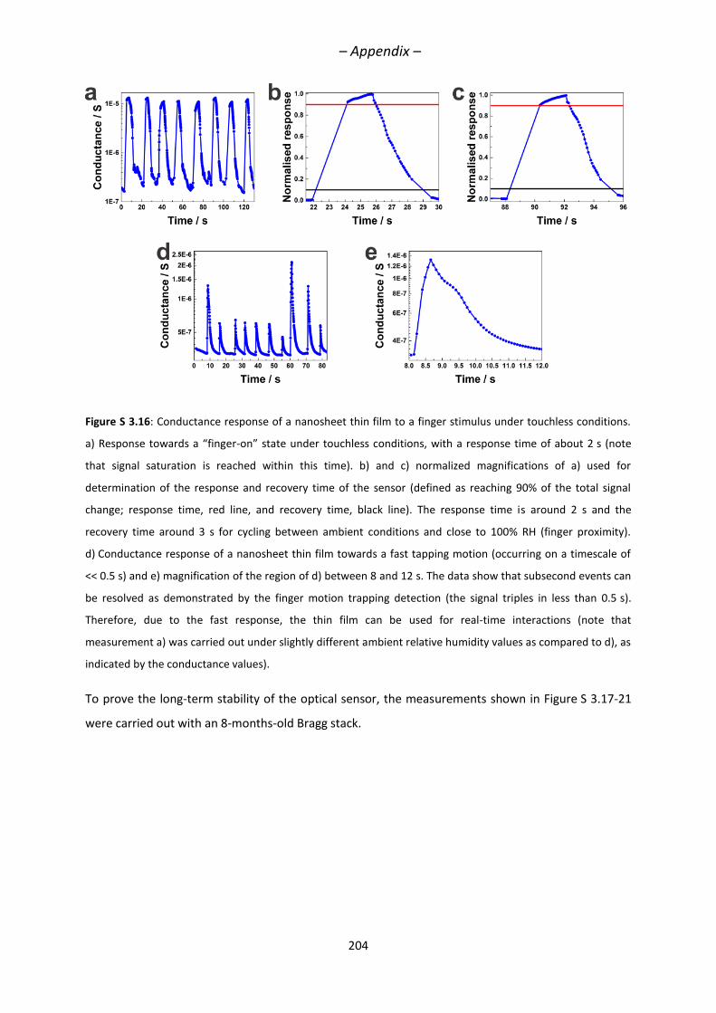
– Appendix –
204
Figure S 3.16: Conductance response of a nanosheet thin film to a finger stimulus under touchless conditions.
a) Response towards a “finger-on” state under touchless conditions, with a response time of about 2 s (note
that signal saturation is reached within this time). b) and c) normalized magnifications of a) used for
determination of the response and recovery time of the sensor (defined as reaching 90% of the total signal
change; response time, red line, and recovery time, black line). The response time is around 2 s and the
recovery time around 3 s for cycling between ambient conditions and close to 100% RH (finger proximity).
d) Conductance response of a nanosheet thin film towards a fast tapping motion (occurring on a timescale of
<< 0.5 s) and e) magnification of the region of d) between 8 and 12 s. The data show that subsecond events can
be resolved as demonstrated by the finger motion trapping detection (the signal triples in less than 0.5 s).
Therefore, due to the fast response, the thin film can be used for real-time interactions (note that
measurement a) was carried out under slightly different ambient relative humidity values as compared to d), as
indicated by the conductance values).
To prove the long-term stability of the optical sensor, the measurements shown in Figure S 3.17-21
were carried out with an 8-months-old Bragg stack.
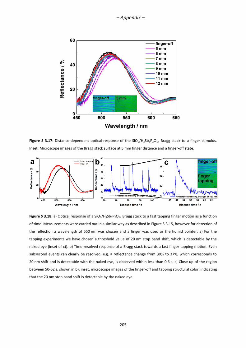
– Appendix –
205
Figure S 3.17: Distance-dependent optical response of the SiO2/H3Sb3P2O14 Bragg stack to a finger stimulus.
Inset: Microscope images of the Bragg stack surface at 5 mm finger distance and a finger-off state.
Figure S 3.18: a) Optical response of a SiO2/H3Sb3P2O14 Bragg stack to a fast tapping finger motion as a function
of time. Measurements were carried out in a similar way as described in Figure S 3.15, however for detection of
the reflection a wavelength of 550 nm was chosen and a finger was used as the humid pointer. a) For the
tapping experiments we have chosen a threshold value of 20 nm stop band shift, which is detectable by the
naked eye (inset of c)). b) Time-resolved response of a Bragg stack towards a fast finger tapping motion. Even
subsecond events can clearly be resolved, e.g. a reflectance change from 30% to 37%, which corresponds to
20 nm shift and is detectable with the naked eye, is observed within less than 0.5 s. c) Close-up of the region
between 50-62 s, shown in b), inset: microscope images of the finger-off and tapping structural color, indicating
that the 20 nm stop band shift is detectable by the naked eye.
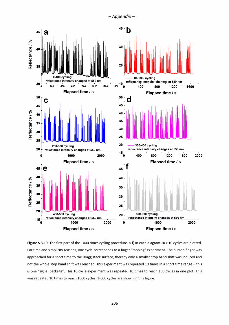
– Appendix –
206
Figure S 3.19: The first part of the 1000 times cycling procedure. a-f) In each diagram 10 x 10 cycles are plotted.
For time and simplicity reasons, one cycle corresponds to a finger “tapping” experiment. The human finger was
approached for a short time to the Bragg stack surface, thereby only a smaller stop band shift was induced and
not the whole stop band shift was reached. This experiment was repeated 10 times in a short time range – this
is one “signal package”. This 10-cycle-experiment was repeated 10 times to reach 100 cycles in one plot. This
was repeated 10 times to reach 1000 cycles. 1-600 cycles are shown in this figure.
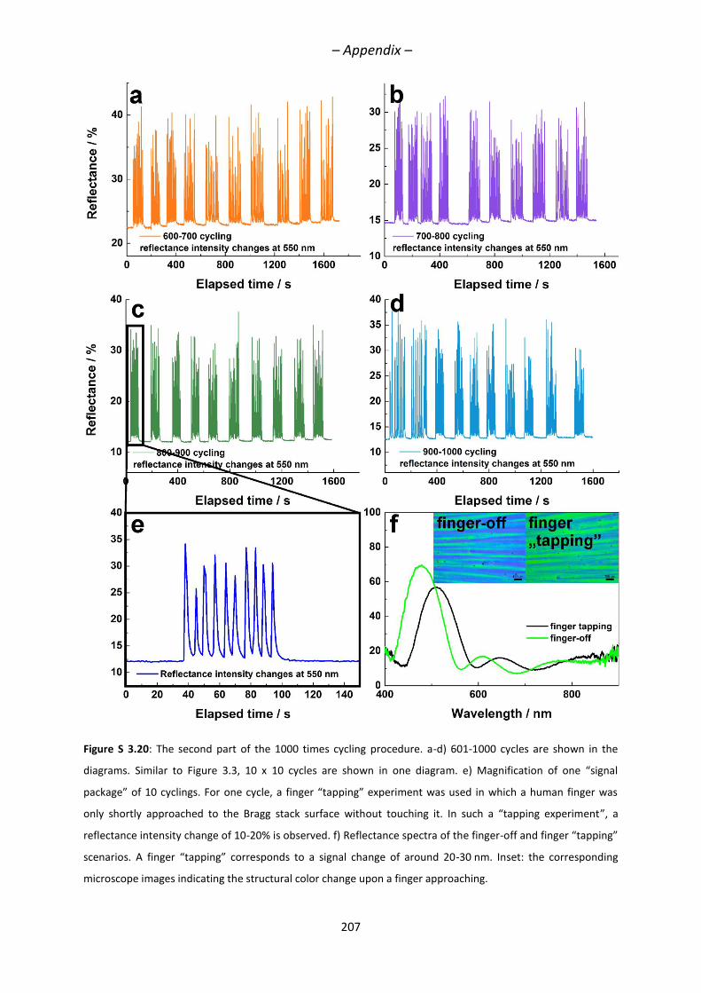
– Appendix –
207
Figure S 3.20: The second part of the 1000 times cycling procedure. a-d) 601-1000 cycles are shown in the
diagrams. Similar to Figure 3.3, 10 x 10 cycles are shown in one diagram. e) Magnification of one “signal
package” of 10 cyclings. For one cycle, a finger “tapping” experiment was used in which a human finger was
only shortly approached to the Bragg stack surface without touching it. In such a “tapping experiment”, a
reflectance intensity change of 10-20% is observed. f) Reflectance spectra of the finger-off and finger “tapping”
scenarios. A finger “tapping” corresponds to a signal change of around 20-30 nm. Inset: the corresponding
microscope images indicating the structural color change upon a finger approaching.
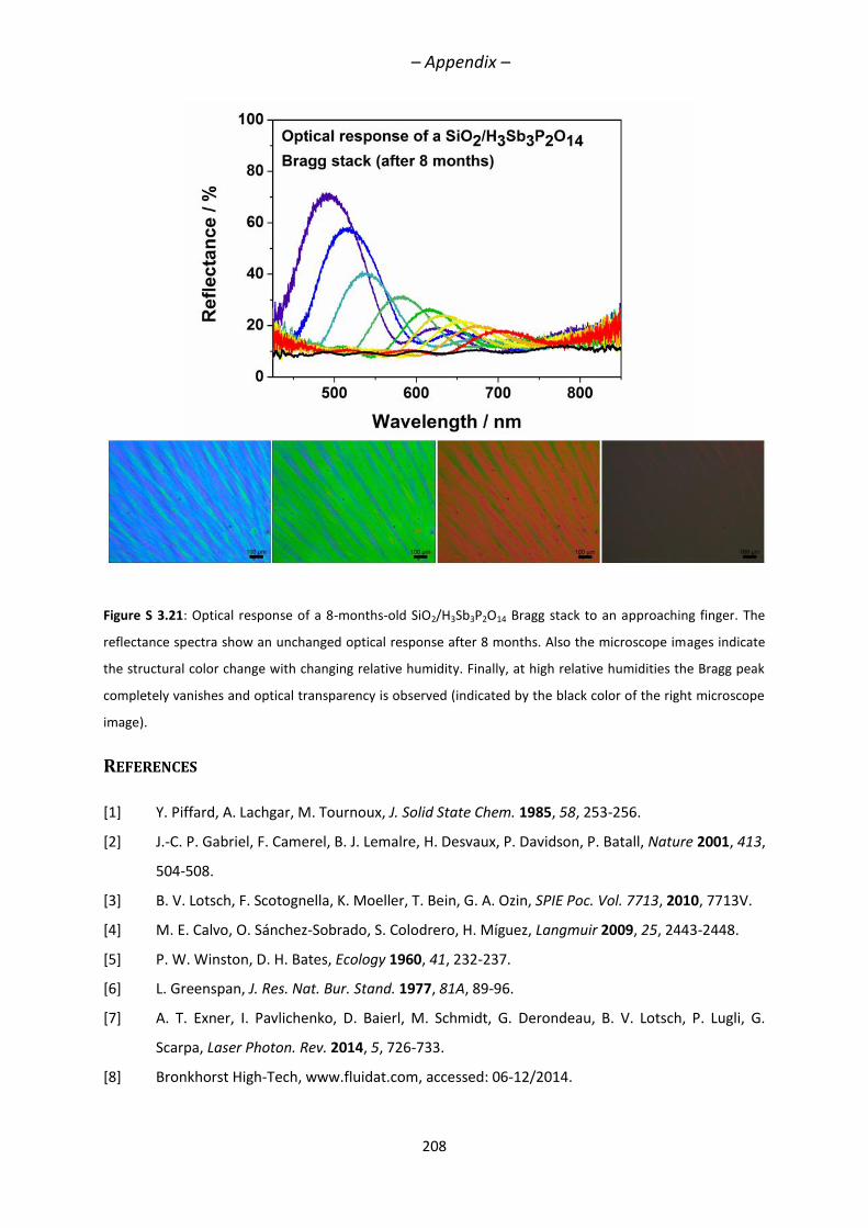
– Appendix –
208
Figure S 3.21: Optical response of a 8-months-old SiO2/H3Sb3P2O14 Bragg stack to an approaching finger. The
reflectance spectra show an unchanged optical response after 8 months. Also the microscope images indicate
the structural color change with changing relative humidity. Finally, at high relative humidities the Bragg peak
completely vanishes and optical transparency is observed (indicated by the black color of the right microscope
image).
REFERENCES
[1] Y. Piffard, A. Lachgar, M. Tournoux, J. Solid State Chem. 1985, 58, 253-256.
[2] J.-C. P. Gabriel, F. Camerel, B. J. Lemalre, H. Desvaux, P. Davidson, P. Batall, Nature 2001, 413,
504-508.
[3] B. V. Lotsch, F. Scotognella, K. Moeller, T. Bein, G. A. Ozin, SPIE Poc. Vol. 7713, 2010, 7713V.
[4] M. E. Calvo, O. Sánchez-Sobrado, S. Colodrero, H. Míguez, Langmuir 2009, 25, 2443-2448.
[5] P. W. Winston, D. H. Bates, Ecology 1960, 41, 232-237.
[6] L. Greenspan, J. Res. Nat. Bur. Stand. 1977, 81A, 89-96.
[7] A. T. Exner, I. Pavlichenko, D. Baierl, M. Schmidt, G. Derondeau, B. V. Lotsch, P. Lugli, G.
Scarpa, Laser Photon. Rev. 2014, 5, 726-733.
[8] Bronkhorst High-Tech, www.fluidat.com, accessed: 06-12/2014.
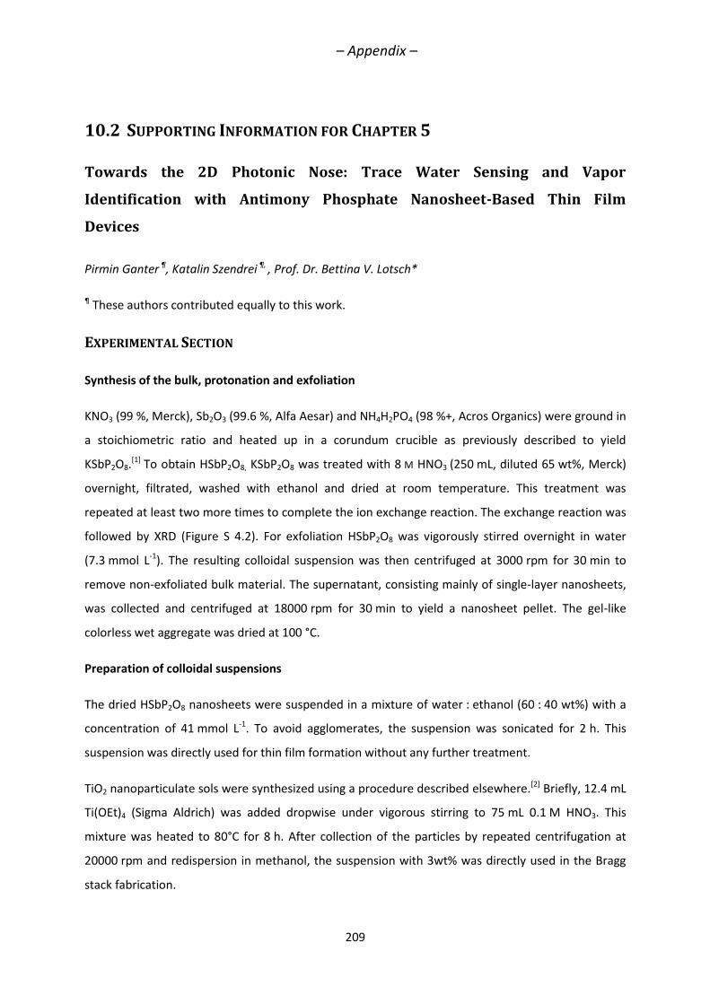
– Appendix –
209
10.2 SUPPORTING INFORMATION FOR CHAPTER 5
Towards the 2D Photonic Nose: Trace Water Sensing and Vapor
Identification with Antimony Phosphate Nanosheet-Based Thin Film
Devices
Pirmin Ganter ¶, Katalin Szendrei ¶, , Prof. Dr. Bettina V. Lotsch*
¶ These authors contributed equally to this work.
EXPERIMENTAL SECTION
Synthesis of the bulk, protonation and exfoliation
KNO3 (99 %, Merck), Sb2O3 (99.6 %, Alfa Aesar) and NH4H2PO4 (98 %+, Acros Organics) were ground in
a stoichiometric ratio and heated up in a corundum crucible as previously described to yield
KSbP2O8.[1]
To obtain HSbP2O8, KSbP2O8 was treated with 8 M HNO3 (250 mL, diluted 65 wt%, Merck)
overnight, filtrated, washed with ethanol and dried at room temperature. This treatment was
repeated at least two more times to complete the ion exchange reaction. The exchange reaction was
followed by XRD (Figure S 4.2). For exfoliation HSbP2O8 was vigorously stirred overnight in water
(7.3 mmol L-1). The resulting colloidal suspension was then centrifuged at 3000 rpm for 30 min to
remove non-exfoliated bulk material. The supernatant, consisting mainly of single-layer nanosheets,
was collected and centrifuged at 18000 rpm for 30 min to yield a nanosheet pellet. The gel-like
colorless wet aggregate was dried at 100 °C.
Preparation of colloidal suspensions
The dried HSbP2O8 nanosheets were suspended in a mixture of water : ethanol (60 : 40 wt%) with a
concentration of 41 mmol L-1. To avoid agglomerates, the suspension was sonicated for 2 h. This
suspension was directly used for thin film formation without any further treatment.
TiO2 nanoparticulate sols were synthesized using a procedure described elsewhere.[2] Briefly, 12.4 mL
Ti(OEt)4 (Sigma Aldrich) was added dropwise under vigorous stirring to 75 mL 0.1 M HNO3. This
mixture was heated to 80°C for 8 h. After collection of the particles by repeated centrifugation at
20000 rpm and redispersion in methanol, the suspension with 3wt% was directly used in the Bragg
stack fabrication.
– Appendix –
210
Fabrication of thin films and Bragg stacks
All thin films and Bragg stacks were fabricated by means of spin-coating using a spin coater (WS-
650S-NPP-Lite, Laurell Technologies Corporation) and colloidal suspensions of the nanosheets and
nanoparticles, respectively, with the colloidal concentrations given above, in the previous section.
For conductance measurements, the redispersed nanosheet colloid was spin-coated at 3000 rpm or
2000 rpm for 1 min with a 10000 rpm s-1 acceleration ramp on a 1.5 cm x 1.5 cm plasma-cleaned
quartz glass substrate. To achieve a sufficient film thickness (around 100 nm) for the conductance
measurements, this deposition step was repeated once. Gold contacts were sputter-coated
(108auto, Cressington) with 180 s sputtering time.
For the Bragg stack fabrication, different film thicknesses were accessed by varying the spin-coating
speed, which allowed for fine-tuning of the optical properties.[3] On plasma cleaned silicon substrates
(1.5 cm x 1.5 cm) 150 µl of the colloidal suspensions were spin-coated alternatingly for 1 min with a
defined speed and heated to 80 °C for 15 min after each layer deposition. 3000 rpm, 4000 rpm and
5000 rpm spin-coating speeds were applied (the same speed for each layer within a Bragg stack) to
tune the optical properties. To create a single nanosheet layer within the Bragg stack, two deposition
steps were applied, both with the same speed, as given above, and further an acceleration rate of
500 rpm s-1 was used. After both deposition steps, the sample was heated to 80°C for 20 min before
the deposition of the next layer. For the TiO2 nanoparticles, an acceleration rate of 5000 rpm s-1 was
applied. The starting and also the last layers are composed of the high RI NPs (TiO2), in order to
ensure the adhesion to the substrate and to increase the refractive index contrast with the
surrounding air.
CHARACTERIZATION
Structural characterization
SEM images of the HSbP2O8 crystals and the nanosheet pellet were acquired with a Vega TS 5130
MM (Tescan) equipped with Si/Li detector (Oxford). Cross-section images of the Bragg stacks were
taken with a Zeiss Merlin FE-SEM. TEM images and selected area electron diffraction (SAD) patterns
were obtained with a Phillips CM30 ST TEM (300 kV, LaB6 cathode) equipped with a Gatan CCD
camera. TEM-EDX analysis was performed with a Si/Li detector (Thermo Fisher, Noran System
Seven). XRD patterns were recorded on a powder X-ray diffractometer (Stadi P, STOE) working with
Ge(111) monochromated Mo-K1 radiation (λ = 70.926 pm) or Cu-K1 radiation (λ = 154.051 pm).
– Appendix –
211
Rietveld refinement of the nanosheet pellet measured in transmission geometry was performed with
the software DiffracPlus TOPAS v4.2 (Bruker AXS). A quasi single layer approach similar to the one
described in the literature was used to approximate the turbostratic disorder.[4,5] The sample showed
preferred orientation effects such that almost exclusively the hk0 reflections were observed, which
allows us to use a simplified model compared to the models as described in the literature, which in
addition include modeling of the 00l reflections. AFM images were acquired on a Veeco CP II system
in non-contact mode. The images of the surfaces of the Bragg stack were obtained with an optical
microscope (Olympus BX51), operating in reflection mode with a 4x objective.
Conductance measurements
To obtain the conductance measurements for relative humidity, two different methodologies were
used. In the first one, the films were kept over saturated salt solutions at around 25 °C[6,7] in a closed
atmosphere at least 20 min before the conductance measurements. In the second one we used an
argon flow set up. A dry Ar flow and a water vapor saturated Ar stream were mixed in different ratios
to define the humidity between 0-93.5%. The setup was calibrated using the conductance values
previously measured at the RH defined by the salt solutions. The cycling experiments were
performed with the Ar flow setup. For sensing trace amounts of water in alcohol (ethanol 99.8%,
water ≤ 0.2%, Roth; 2-propanol 99.8%,water ≤ 0.05%, Merck) water mixtures, an Ar stream at a
constant rate of 8.4 L min-1 was passed through 100 mL of solution. By passing an Ar stream through
the solution the stream takes up certain amounts of moisture and ethanol, which leads to a change
in the conductance of the thin film sensor.
The change in conductance was monitored by impedance spectroscopy (in-plane geometry, two
point measurement) with an impedance bridge (Princeton Applied Research, VersaSTAT MC)
applying an AC voltage of 500 mV and a frequency range of 1 Hz to 1 MHz. Cycling measurements
were performed with a fixed frequency of 300 Hz.
Optical characterization
Porosimetry measurements were carried out by the porosimetry tool of Sopra PS-1000 SAM,
whereby the sample was equilibrated at all water vapor relative pressure values for 15 min. The
measurement results were fitted with the software Sopra SAE using the model combination Cauchy
and Lorentz. The thickness of the nanoparticle layers was confirmed by ellipsometry to be constant
with changing vapor relative pressure and only the refractive index was fitted. For the nanosheet thin
films, both the layer thickness and the refractive index were fitted over the relative pressure range
simultaneously. Prior to all measurements, the nanoparticle samples were heated for at least 30 min
at 200 °C and the nanosheets thin films for 30 min at 60 °C in vacuum to make sure that the pores
– Appendix –
212
are empty. To obtain the optical isotherms, all fitted measurement results were plotted against the
analyte relative pressure.
All optical spectra were measured with a fiber optic spectrometer (USB2000+, Ocean Optics)
attached to a microscope (DM2500, Leica) with normal incidence and the optical spectra were always
taken at the same spot (1×1 mm2 in area).
To obtain the optical changes with changes in relative humidity, the Bragg stacks were kept in a
stainless steel chamber with a total volume of 5 mL and with a transparent glass window. In the
chamber, 0.7 mL of saturated salt solutions[6,7] were filled without touching the sample surface, and
kept at around 25 °C to define the humidity in the closed atmosphere. At each step, 20 min
equilibration time was needed.
To measure the response to solvent vapors and the saturation times for all analytes (including the
cycling experiments), a mass flow controller with a controlled evaporation mixer (CEM) (see below)
was applied. To measure the saturation time, the reflectance intensity changes of the Bragg peak
were observed at a certain wavelength placed at the red stop band edge. While the Bragg peak shifts
as a response to the analyte exposure, the reflectance intensity changes at the observed wavelength.
The full response from 0% to 100% vapor relative pressure was taken defined as the saturation time.
In these dynamic measurements, the BSs were placed into a closed chamber with the dimensions of
2.5x2.5x0.5 cm3, where well-defined vapor relative pressure values were realized by connecting the
inserted pipette tip with a liquid-gas flow controller (Bronkhorst) and a vaporizer (CEM) with a
massflow-controlled carrier gas flow. To observe a specific solvent vapor relative pressure, the carrier
gas nitrogen (200 mL min-1) and the liquid solvent were dosed into the CEM (controlled evaporation
and mixing, W101A-130-K, Bronkhorst High-Tech), where the thermal evaporation of the solvent
took place. The CEM was heated to temperatures slightly above the boiling point. The relative vapor
pressures were calculated via the software FLUIDAT (CEM calculation), which considers the actual
atmospheric pressure, the temperature and the properties of the analyte (vapor pressure, heat
capacity).[8] The obtained data were analyzed with the SPECTRA SUITE (2008) software.
Simulations
Simulations of the reflectance spectra were carried out using a Matlab code based on a full-vector
calculation using the transfer matrix method.[9] The layer thicknesses at 0% RH and 0% analyte
relative pressure were taken from the SEM cross section images. The refractive indices were taken
from the porosimetry measurements. For the simulations of the selectivity measurements, the layer
thicknesses at 100% were fitted according to the measured reflectance spectra. The refractive indices
in the optical isotherms are given at 623 nm.
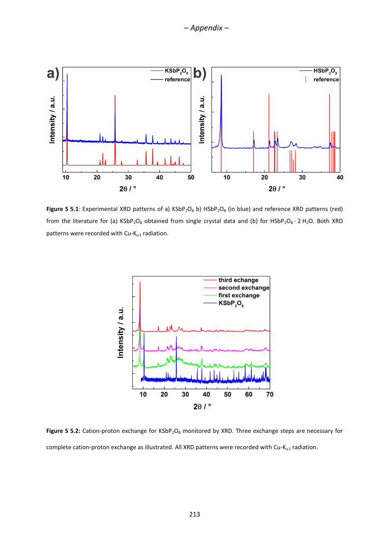
– Appendix –
213
Figure S 5.1: Experimental XRD patterns of a) KSbP2O8 b) HSbP2O8 (in blue) and reference XRD patterns (red)
from the literature for (a) KSbP2O8 obtained from single crystal data and (b) for HSbP2O8 ∙ 2 H2O. Both XRD
patterns were recorded with Cu-K1 radiation.
Figure S 5.2: Cation-proton exchange for KSbP2O8 monitored by XRD. Three exchange steps are necessary for
complete cation-proton exchange as illustrated. All XRD patterns were recorded with Cu-K1 radiation.
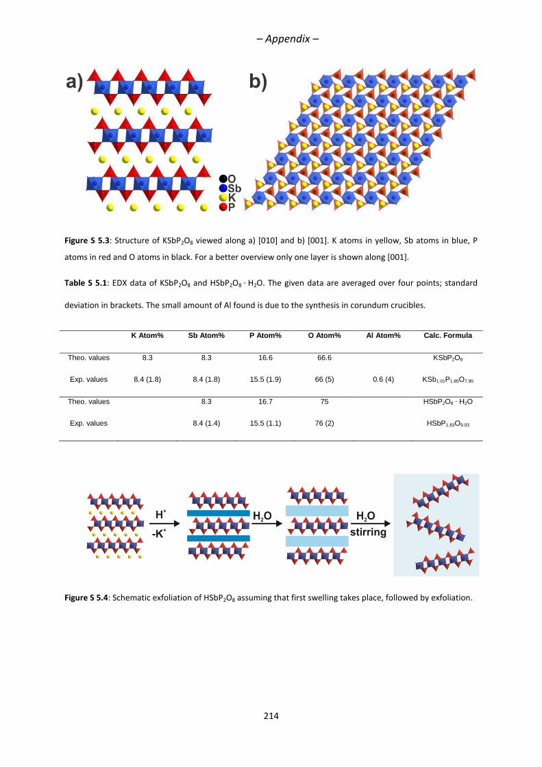
– Appendix –
214
Figure S 5.3: Structure of KSbP2O8 viewed along a) [010] and b) [001]. K atoms in yellow, Sb atoms in blue, P
atoms in red and O atoms in black. For a better overview only one layer is shown along [001].
Table S 5.1: EDX data of KSbP2O8 and HSbP2O8 ∙ H2O. The given data are averaged over four points; standard
deviation in brackets. The small amount of Al found is due to the synthesis in corundum crucibles.
K Atom% Sb Atom% P Atom% O Atom% Al Atom% Calc. Formula
Theo. values 8.3 8.3 16.6 66.6 KSbP2O8
Exp. values 8.4 (1.8) 8.4 (1.8) 15.5 (1.9) 66 (5) 0.6 (4) KSb1.01P1.85O7.95
Theo. values 8.3 16.7 75 HSbP2O8 ∙ H2O
Exp. values 8.4 (1.4) 15.5 (1.1) 76 (2) HSbP1.83O9.03
Figure S 5.4: Schematic exfoliation of HSbP2O8 assuming that first swelling takes place, followed by exfoliation.
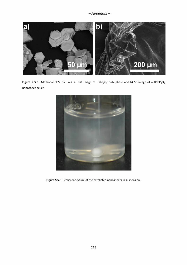
– Appendix –
215
Figure S 5.5: Additional SEM pictures. a) BSE image of HSbP2O8 bulk phase and b) SE image of a HSbP2O8
nanosheet pellet.
Figure S 5.6: Schlieren texture of the exfoliated nanosheets in suspension.
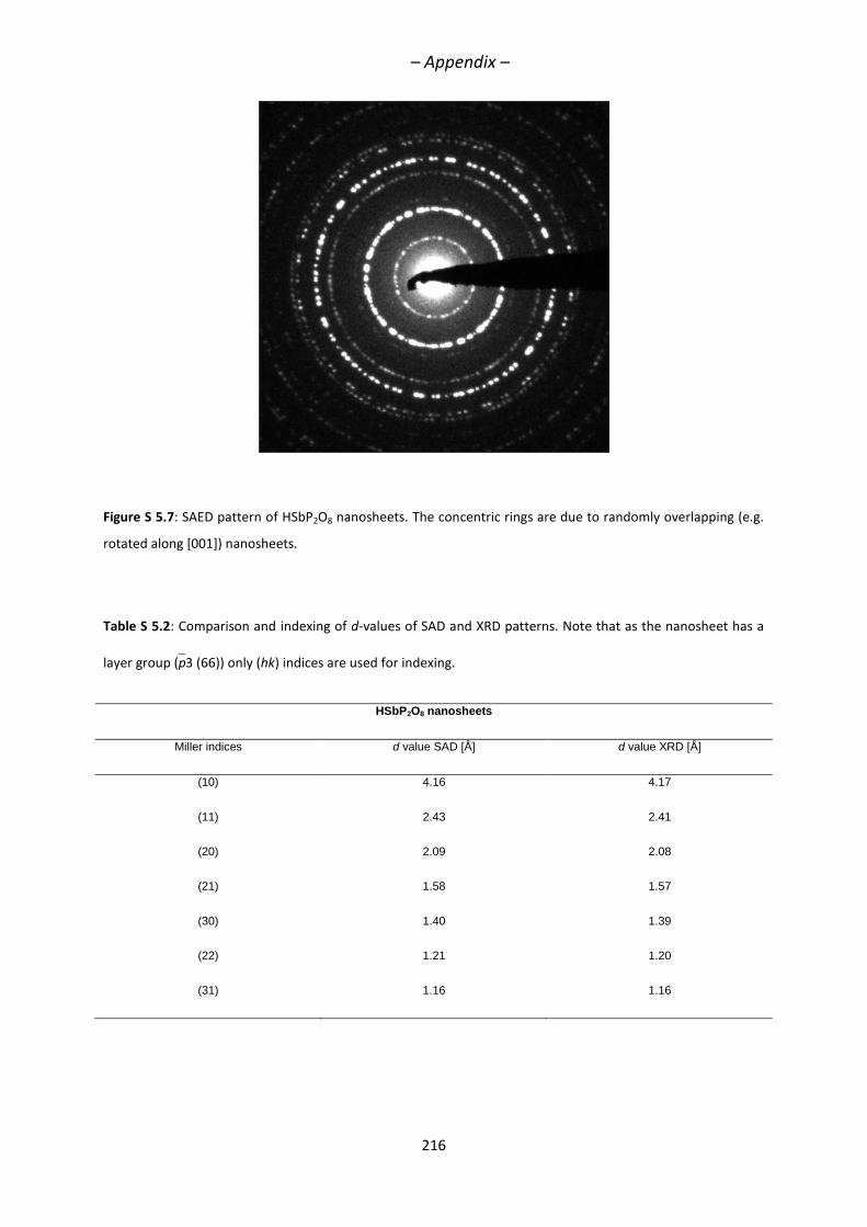
– Appendix –
216
Figure S 5.7: SAED pattern of HSbP2O8 nanosheets. The concentric rings are due to randomly overlapping (e.g.
rotated along [001]) nanosheets.
Table S 5.2: Comparison and indexing of d-values of SAD and XRD patterns. Note that as the nanosheet has a
layer group (p3 (66)) only (hk) indices are used for indexing.
HSbP2O8 nanosheets
Miller indices d value SAD [Å] d value XRD [Å]
(10) 4.16 4.17
(11) 2.43 2.41
(20) 2.09 2.08
(21) 1.58 1.57
(30) 1.40 1.39
(22) 1.21 1.20
(31) 1.16 1.16
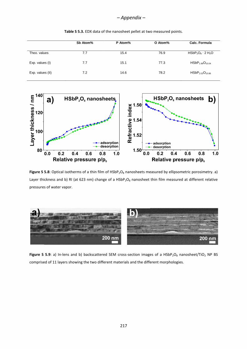
– Appendix –
217
Table S 5.3. EDX data of the nanosheet pellet at two measured points.
Sb Atom% P Atom% O Atom% Calc. Formula
Theo. values 7.7 15.4 76.9 HSbP2O8 ∙ 2 H2O
Exp. values (I) 7.7 15.1 77.3 HSbP1.96O10.04
Exp. values (II) 7.2 14.6 78.2 HSbP2.02O10.86
Figure S 5.8: Optical isotherms of a thin film of HSbP2O8 nanosheets measured by ellipsometric porosimetry. a)
Layer thickness and b) RI (at 623 nm) change of a HSbP2O8 nanosheet thin film measured at different relative
pressures of water vapor.
Figure S 5.9: a) In-lens and b) backscattered SEM cross-section images of a HSbP2O8 nanosheet/TiO2 NP BS
comprised of 11 layers showing the two different materials and the different morphologies.
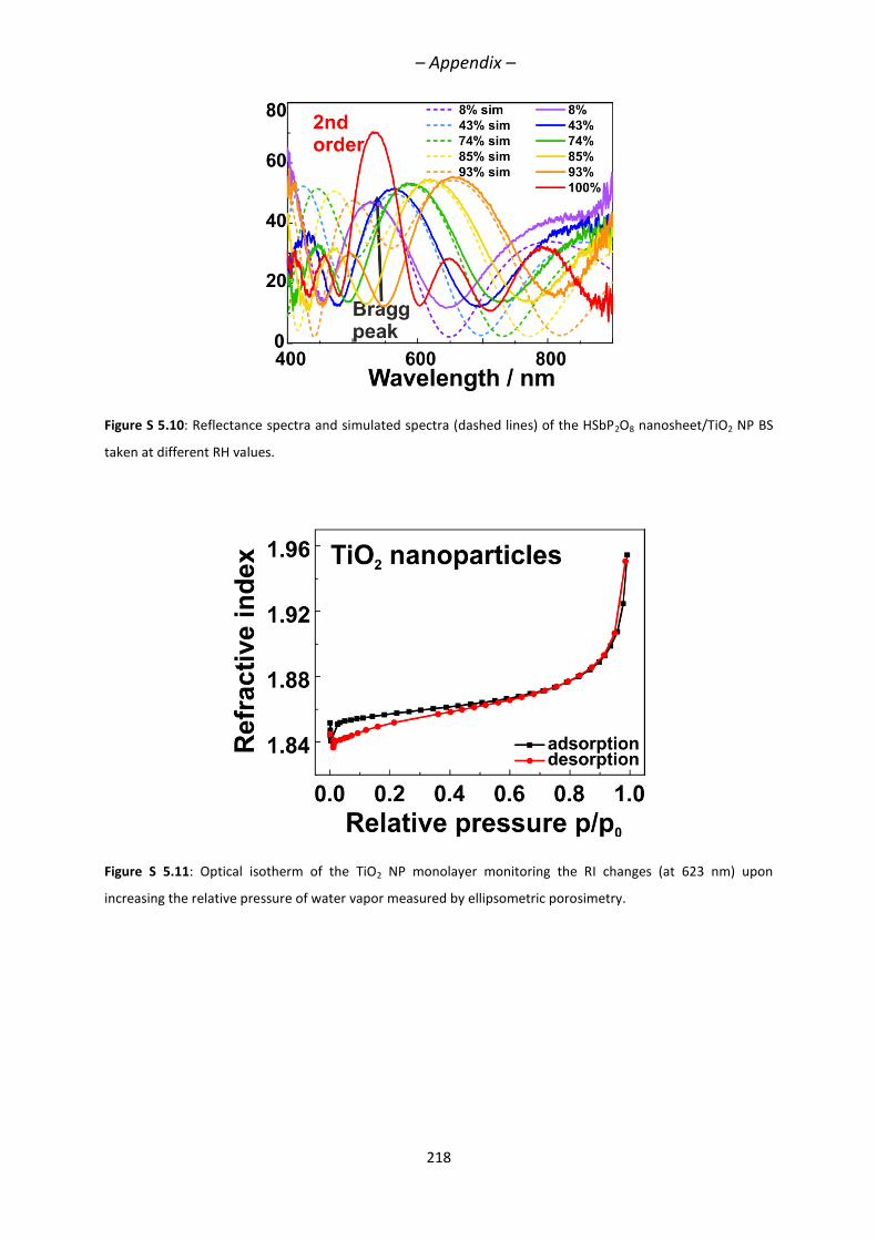
– Appendix –
218
Figure S 5.10: Reflectance spectra and simulated spectra (dashed lines) of the HSbP2O8 nanosheet/TiO2 NP BS
taken at different RH values.
Figure S 5.11: Optical isotherm of the TiO2 NP monolayer monitoring the RI changes (at 623 nm) upon
increasing the relative pressure of water vapor measured by ellipsometric porosimetry.
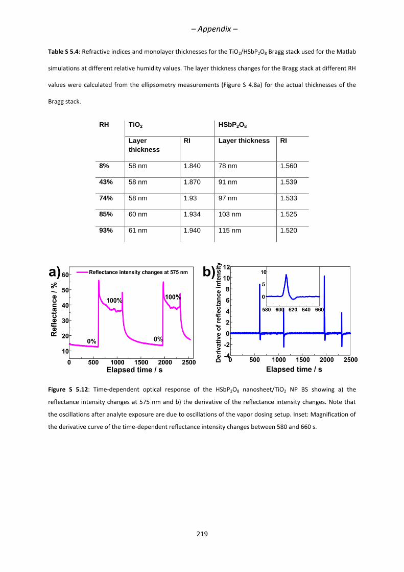
– Appendix –
219
Table S 5.4: Refractive indices and monolayer thicknesses for the TiO2/HSbP2O8 Bragg stack used for the Matlab
simulations at different relative humidity values. The layer thickness changes for the Bragg stack at different RH
values were calculated from the ellipsometry measurements (Figure S 4.8a) for the actual thicknesses of the
Bragg stack.
RH TiO2 HSbP2O8
Layer
thickness
RI Layer thickness RI
8% 58 nm 1.840 78 nm 1.560
43% 58 nm 1.870 91 nm 1.539
74% 58 nm 1.93 97 nm 1.533
85% 60 nm 1.934 103 nm 1.525
93% 61 nm 1.940 115 nm 1.520
Figure S 5.12: Time-dependent optical response of the HSbP2O8 nanosheet/TiO2 NP BS showing a) the
reflectance intensity changes at 575 nm and b) the derivative of the reflectance intensity changes. Note that
the oscillations after analyte exposure are due to oscillations of the vapor dosing setup. Inset: Magnification of
the derivative curve of the time-dependent reflectance intensity changes between 580 and 660 s.
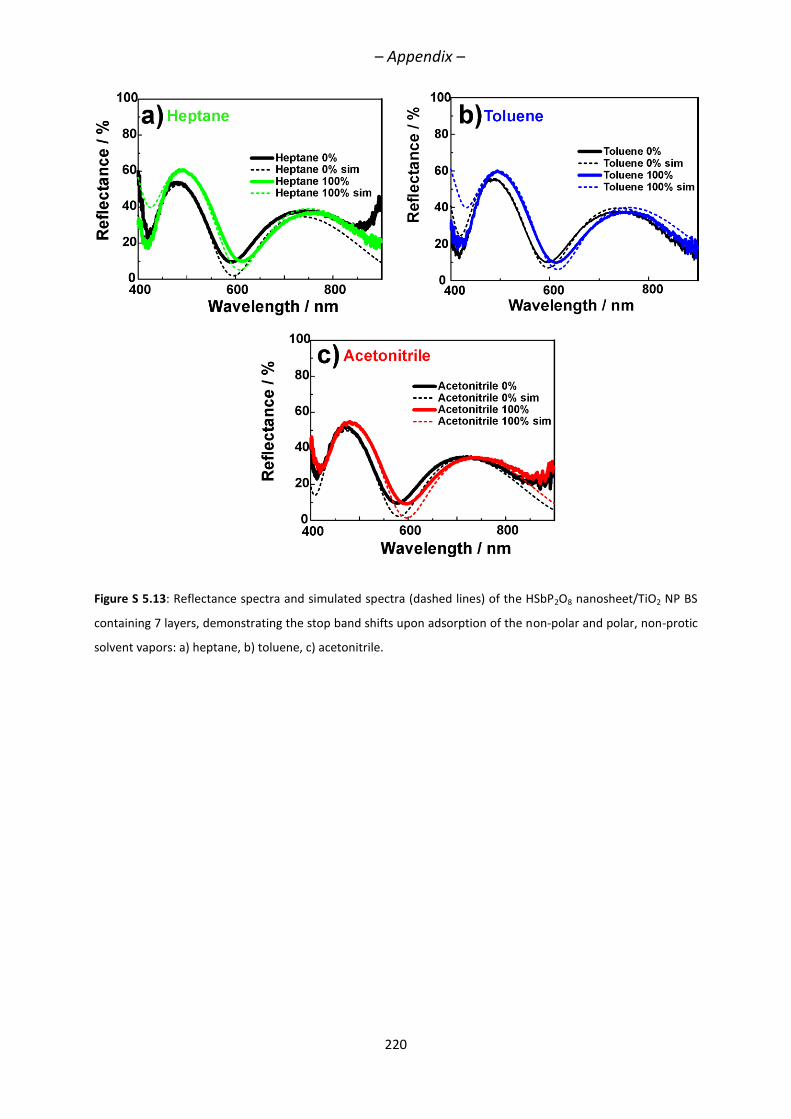
– Appendix –
220
Figure S 5.13: Reflectance spectra and simulated spectra (dashed lines) of the HSbP2O8 nanosheet/TiO2 NP BS
containing 7 layers, demonstrating the stop band shifts upon adsorption of the non-polar and polar, non-protic
solvent vapors: a) heptane, b) toluene, c) acetonitrile.
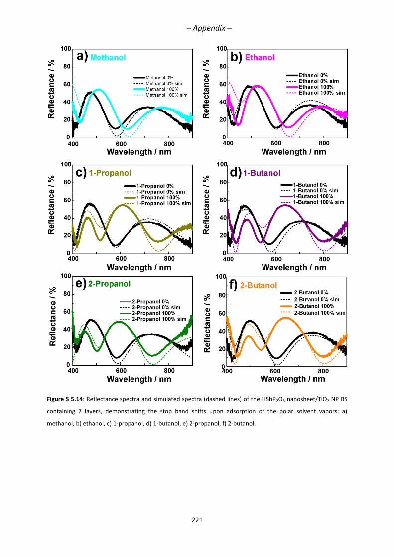
– Appendix –
221
Figure S 5.14: Reflectance spectra and simulated spectra (dashed lines) of the HSbP2O8 nanosheet/TiO2 NP BS
containing 7 layers, demonstrating the stop band shifts upon adsorption of the polar solvent vapors: a)
methanol, b) ethanol, c) 1-propanol, d) 1-butanol, e) 2-propanol, f) 2-butanol.
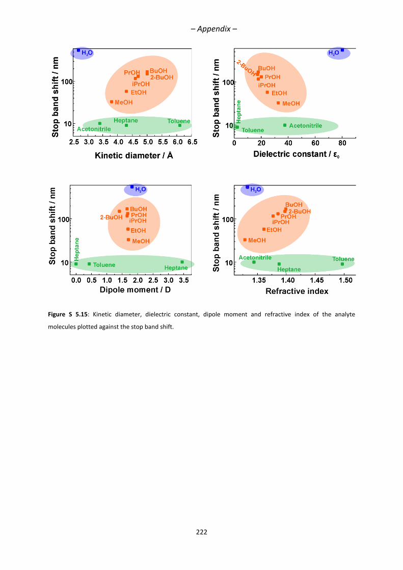
– Appendix –
222
Figure S 5.15: Kinetic diameter, dielectric constant, dipole moment and refractive index of the analyte
molecules plotted against the stop band shift.
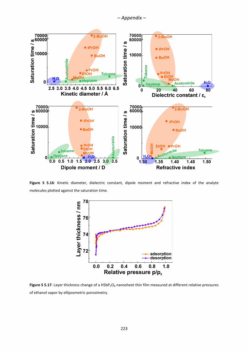
– Appendix –
223
Figure S 5.16: Kinetic diameter, dielectric constant, dipole moment and refractive index of the analyte
molecules plotted against the saturation time.
Figure S 5.17: Layer thickness change of a HSbP2O8 nanosheet thin film measured at different relative pressures
of ethanol vapor by ellipsometric porosimetry.
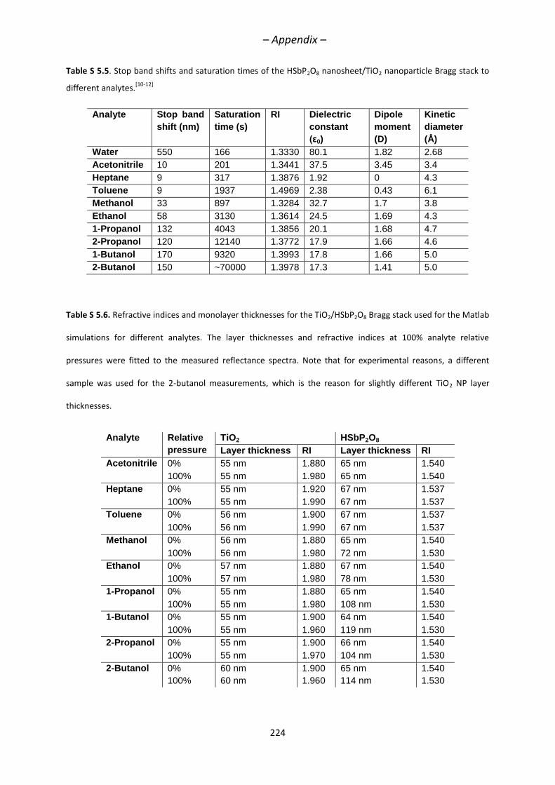
– Appendix –
224
Table S 5.5. Stop band shifts and saturation times of the HSbP2O8 nanosheet/TiO2 nanoparticle Bragg stack to
different analytes.[10-12]
Analyte Stop band
shift (nm)
Saturation
time (s)
RI Dielectric
constant
(ε0)
Dipole
moment
(D)
Kinetic
diameter
(Å)
Water 550 166 1.3330 80.1 1.82 2.68
Acetonitrile 10 201 1.3441 37.5 3.45 3.4
Heptane 9 317 1.3876 1.92 0 4.3
Toluene 9 1937 1.4969 2.38 0.43 6.1
Methanol 33 897 1.3284 32.7 1.7 3.8
Ethanol 58 3130 1.3614 24.5 1.69 4.3
1-Propanol 132 4043 1.3856 20.1 1.68 4.7
2-Propanol 120 12140 1.3772 17.9 1.66 4.6
1-Butanol 170 9320 1.3993 17.8 1.66 5.0
2-Butanol 150 ~70000 1.3978 17.3 1.41 5.0
Table S 5.6. Refractive indices and monolayer thicknesses for the TiO2/HSbP2O8 Bragg stack used for the Matlab
simulations for different analytes. The layer thicknesses and refractive indices at 100% analyte relative
pressures were fitted to the measured reflectance spectra. Note that for experimental reasons, a different
sample was used for the 2-butanol measurements, which is the reason for slightly different TiO2 NP layer
thicknesses.
Analyte Relative
pressure
TiO2 HSbP2O8
Layer thickness RI Layer thickness RI
Acetonitrile 0% 55 nm 1.880 65 nm 1.540
100% 55 nm 1.980 65 nm 1.540
Heptane 0% 55 nm 1.920 67 nm 1.537
100% 55 nm 1.990 67 nm 1.537
Toluene 0% 56 nm 1.900 67 nm 1.537
100% 56 nm 1.990 67 nm 1.537
Methanol 0% 56 nm 1.880 65 nm 1.540
100% 56 nm 1.980 72 nm 1.530
Ethanol 0% 57 nm 1.880 67 nm 1.540
100% 57 nm 1.980 78 nm 1.530
1-Propanol 0% 55 nm 1.880 65 nm 1.540
100% 55 nm 1.980 108 nm 1.530
1-Butanol 0% 55 nm 1.900 64 nm 1.540
100% 55 nm 1.960 119 nm 1.530
2-Propanol 0% 55 nm 1.900 66 nm 1.540
100% 55 nm 1.970 104 nm 1.530
2-Butanol 0% 60 nm 1.900 65 nm 1.540
100% 60 nm 1.960 114 nm 1.530
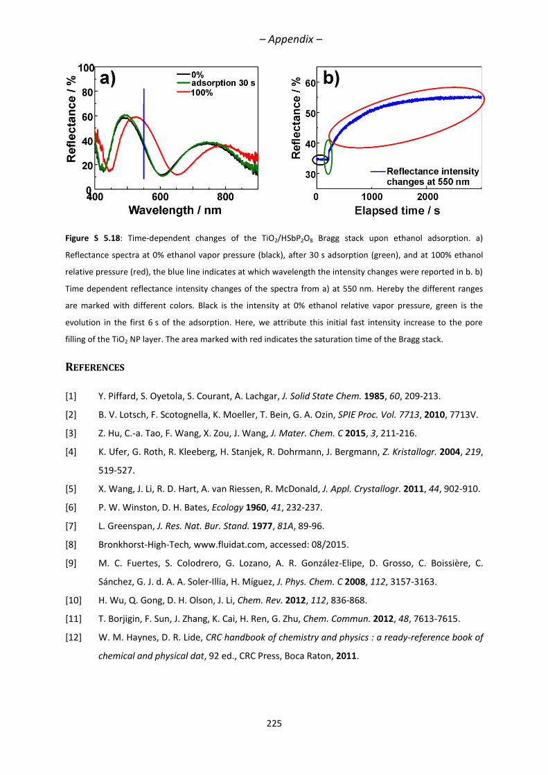
– Appendix –
225
Figure S 5.18: Time-dependent changes of the TiO2/HSbP2O8 Bragg stack upon ethanol adsorption. a)
Reflectance spectra at 0% ethanol vapor pressure (black), after 30 s adsorption (green), and at 100% ethanol
relative pressure (red), the blue line indicates at which wavelength the intensity changes were reported in b. b)
Time dependent reflectance intensity changes of the spectra from a) at 550 nm. Hereby the different ranges
are marked with different colors. Black is the intensity at 0% ethanol relative vapor pressure, green is the
evolution in the first 6 s of the adsorption. Here, we attribute this initial fast intensity increase to the pore
filling of the TiO2 NP layer. The area marked with red indicates the saturation time of the Bragg stack.
REFERENCES
[1] Y. Piffard, S. Oyetola, S. Courant, A. Lachgar, J. Solid State Chem. 1985, 60, 209-213.
[2] B. V. Lotsch, F. Scotognella, K. Moeller, T. Bein, G. A. Ozin, SPIE Proc. Vol. 7713, 2010, 7713V.
[3] Z. Hu, C.-a. Tao, F. Wang, X. Zou, J. Wang, J. Mater. Chem. C 2015, 3, 211-216.
[4] K. Ufer, G. Roth, R. Kleeberg, H. Stanjek, R. Dohrmann, J. Bergmann, Z. Kristallogr. 2004, 219,
519-527.
[5] X. Wang, J. Li, R. D. Hart, A. van Riessen, R. McDonald, J. Appl. Crystallogr. 2011, 44, 902-910.
[6] P. W. Winston, D. H. Bates, Ecology 1960, 41, 232-237.
[7] L. Greenspan, J. Res. Nat. Bur. Stand. 1977, 81A, 89-96.
[8] Bronkhorst-High-Tech, www.fluidat.com, accessed: 08/2015.
[9] M. C. Fuertes, S. Colodrero, G. Lozano, A. R. González-Elipe, D. Grosso, C. Boissière, C.
Sánchez, G. J. d. A. A. Soler-Illia, H. Míguez, J. Phys. Chem. C 2008, 112, 3157-3163.
[10] H. Wu, Q. Gong, D. H. Olson, J. Li, Chem. Rev. 2012, 112, 836-868.
[11] T. Borjigin, F. Sun, J. Zhang, K. Cai, H. Ren, G. Zhu, Chem. Commun. 2012, 48, 7613-7615.
[12] W. M. Haynes, D. R. Lide, CRC handbook of chemistry and physics : a ready-reference book of
chemical and physical dat, 92 ed., CRC Press, Boca Raton, 2011.
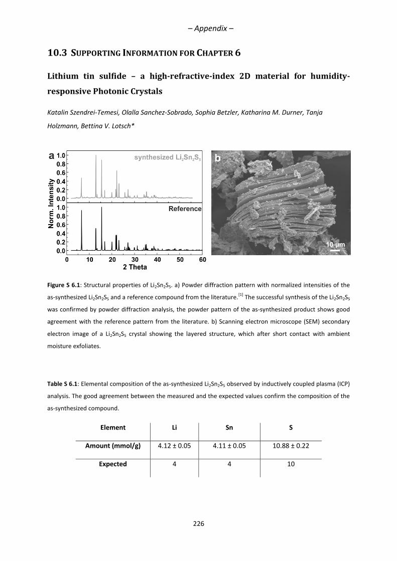
– Appendix –
226
10.3 SUPPORTING INFORMATION FOR CHAPTER 6
Lithium tin sulfide – a high-refractive-index 2D material for humidity-
responsive Photonic Crystals
Katalin Szendrei-Temesi, Olalla Sanchez-Sobrado, Sophia Betzler, Katharina M. Durner, Tanja
Holzmann, Bettina V. Lotsch*
Figure S 6.1: Structural properties of Li2Sn2S5. a) Powder diffraction pattern with normalized intensities of the
as-synthesized Li2Sn2S5 and a reference compound from the literature.[1]
The successful synthesis of the Li2Sn2S5
was confirmed by powder diffraction analysis, the powder pattern of the as-synthesized product shows good
agreement with the reference pattern from the literature. b) Scanning electron microscope (SEM) secondary
electron image of a Li2Sn2S5 crystal showing the layered structure, which after short contact with ambient
moisture exfoliates.
Table S 6.1: Elemental composition of the as-synthesized Li2Sn2S5 observed by inductively coupled plasma (ICP)
analysis. The good agreement between the measured and the expected values confirm the composition of the
as-synthesized compound.
Element Li Sn S
Amount (mmol/g) 4.12 ± 0.05 4.11 ± 0.05 10.88 ± 0.22
Expected 4 4 10
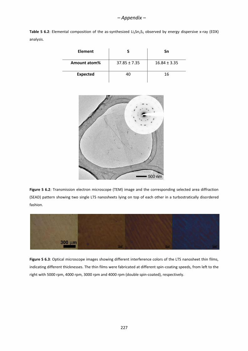
– Appendix –
227
Table S 6.2: Elemental composition of the as-synthesized Li2Sn2S5 observed by energy dispersive x-ray (EDX)
analysis.
Element S Sn
Amount atom% 37.85 ± 7.35 16.84 ± 3.35
Expected 40 16
Figure S 6.2: Transmission electron microscope (TEM) image and the corresponding selected area diffraction
(SEAD) pattern showing two single LTS nanosheets lying on top of each other in a turbostratically disordered
fashion.
Figure S 6.3: Optical microscope images showing different interference colors of the LTS nanosheet thin films,
indicating different thicknesses. The thin films were fabricated at different spin-coating speeds, from left to the
right with 5000 rpm, 4000 rpm, 3000 rpm and 4000 rpm (double spin-coated), respectively.
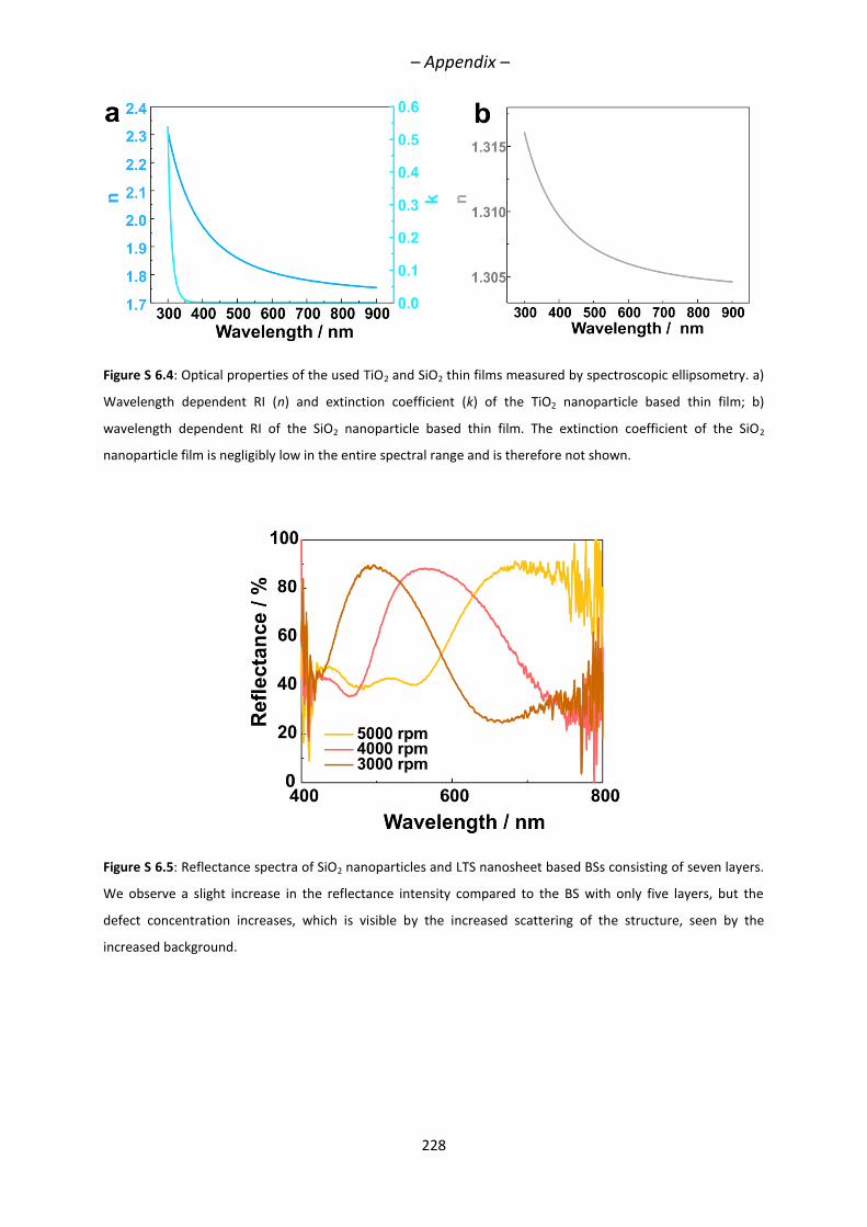
– Appendix –
228
Figure S 6.4: Optical properties of the used TiO2 and SiO2 thin films measured by spectroscopic ellipsometry. a)
Wavelength dependent RI (n) and extinction coefficient (k) of the TiO2 nanoparticle based thin film; b)
wavelength dependent RI of the SiO2 nanoparticle based thin film. The extinction coefficient of the SiO2
nanoparticle film is negligibly low in the entire spectral range and is therefore not shown.
Figure S 6.5: Reflectance spectra of SiO2 nanoparticles and LTS nanosheet based BSs consisting of seven layers.
We observe a slight increase in the reflectance intensity compared to the BS with only five layers, but the
defect concentration increases, which is visible by the increased scattering of the structure, seen by the
increased background.
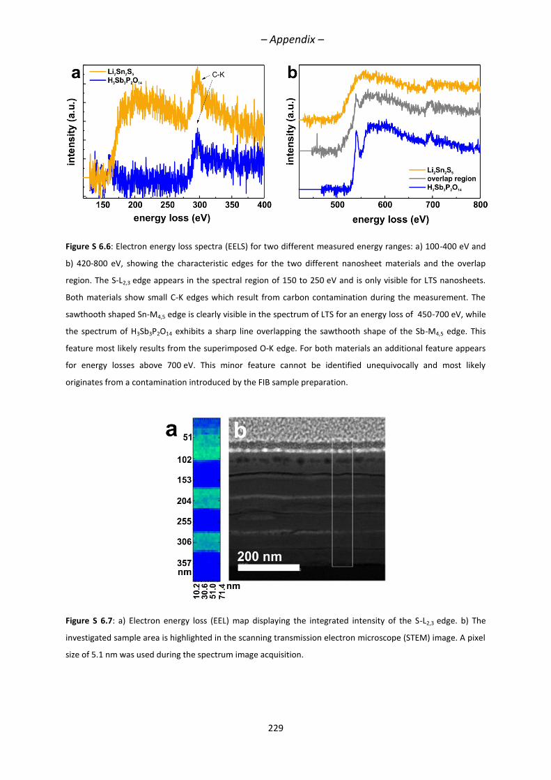
– Appendix –
229
Figure S 6.6: Electron energy loss spectra (EELS) for two different measured energy ranges: a) 100-400 eV and
b) 420-800 eV, showing the characteristic edges for the two different nanosheet materials and the overlap
region. The S-L2,3 edge appears in the spectral region of 150 to 250 eV and is only visible for LTS nanosheets.
Both materials show small C-K edges which result from carbon contamination during the measurement. The
sawthooth shaped Sn-M4,5 edge is clearly visible in the spectrum of LTS for an energy loss of 450-700 eV, while
the spectrum of H3Sb3P2O14 exhibits a sharp line overlapping the sawthooth shape of the Sb-M4,5 edge. This
feature most likely results from the superimposed O-K edge. For both materials an additional feature appears
for energy losses above 700 eV. This minor feature cannot be identified unequivocally and most likely
originates from a contamination introduced by the FIB sample preparation.
Figure S 6.7: a) Electron energy loss (EEL) map displaying the integrated intensity of the S-L2,3 edge. b) The
investigated sample area is highlighted in the scanning transmission electron microscope (STEM) image. A pixel
size of 5.1 nm was used during the spectrum image acquisition.
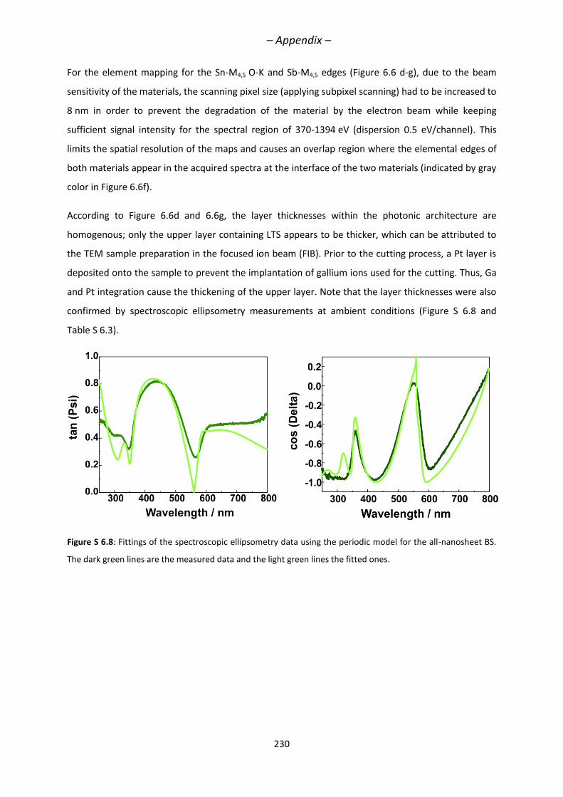
– Appendix –
230
For the element mapping for the Sn-M4,5 O-K and Sb-M4,5 edges (Figure 6.6 d-g), due to the beam
sensitivity of the materials, the scanning pixel size (applying subpixel scanning) had to be increased to
8 nm in order to prevent the degradation of the material by the electron beam while keeping
sufficient signal intensity for the spectral region of 370-1394 eV (dispersion 0.5 eV/channel). This
limits the spatial resolution of the maps and causes an overlap region where the elemental edges of
both materials appear in the acquired spectra at the interface of the two materials (indicated by gray
color in Figure 6.6f).
According to Figure 6.6d and 6.6g, the layer thicknesses within the photonic architecture are
homogenous; only the upper layer containing LTS appears to be thicker, which can be attributed to
the TEM sample preparation in the focused ion beam (FIB). Prior to the cutting process, a Pt layer is
deposited onto the sample to prevent the implantation of gallium ions used for the cutting. Thus, Ga
and Pt integration cause the thickening of the upper layer. Note that the layer thicknesses were also
confirmed by spectroscopic ellipsometry measurements at ambient conditions (Figure S 6.8 and
Table S 6.3).
Figure S 6.8: Fittings of the spectroscopic ellipsometry data using the periodic model for the all-nanosheet BS.
The dark green lines are the measured data and the light green lines the fitted ones.
– Appendix –
231
Figure S 6.9: Cycling behavior of the SiO2 / LTS nanosheet based Bragg stack. The cycling was performed by
alternatingly applying 11% and 93% relative pressure of water vapor. The spectral changes were detected by
recording the reflectance intensity at 450 nm. This wavelength was carefully chosen to monitor the changes at
the blue stopband edge, which are measurable for the humidity range between 10-93% RH. Please note that
due to the stopband shift, a decrease of the reflectance intensity refers to an increase in the relative humidity,
as marked in b).
Figure S 6.10: Cycling behavior of the H3Sb3P2O14 / LTS nanosheet based Bragg stack. The cycling was
performed by applying 11% and 93% relative pressure of water vapor. The spectral changes were detected by
recording the reflectance intensity at 550 nm. This wavelength was carefully chosen to monitor the changes at
the red stopband edge, which are measurable for the humidity range between 10-93% RH. Please note that
due to the stopband shift, a decrease of the reflectance intensity refers to a decrease in the relative humidity,
as marked in b).
– Appendix –
232
Figure S 6.11: Time dependent reflectance intensity changes at 450 nm and 550 nm, respectively, of a) the SiO2
and b) the H3Sb3P2O14 based LTS Bragg stacks. The plots show an excerpt of the time plots shown in S 6.9 and
6.10 in order to demonstrate the calculation of the response times (τ63).
Figure S 6.12: Reflectance spectra of the a) SiO2 / LTS and b) H3Sb3P2O14 / LTS based Bragg stack showing the
stable cycling behavior between 100% RH and ambient (30% RH) conditions. The features of the reflectance
spectra at 100% RH arise from Fabry-Perot oscillations, since at 100% RH the RI contrast cancels out and the
structure appears transparent.
Table S 6.3: Fitted layer thicknesses and refractive indices for the two different layer materials measured by
spectroscopic ellipsometry using the periodic model for 3 double layers.
Layer material LTS H3Sb3P2O14
Thickness 44 nm 64 nm
Refractive index (at 633 nm) 2.65 1.56
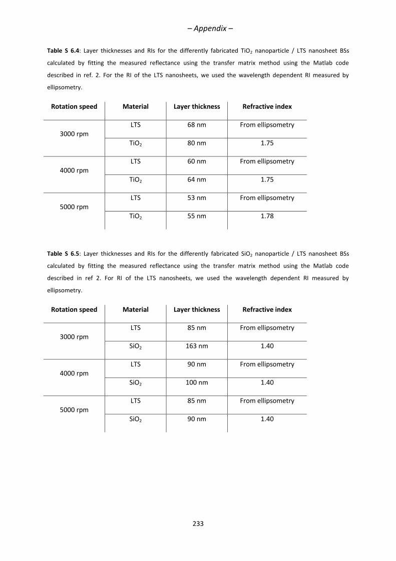
– Appendix –
233
Table S 6.4: Layer thicknesses and RIs for the differently fabricated TiO2 nanoparticle / LTS nanosheet BSs
calculated by fitting the measured reflectance using the transfer matrix method using the Matlab code
described in ref. 2. For the RI of the LTS nanosheets, we used the wavelength dependent RI measured by
ellipsometry.
Rotation speed Material Layer thickness Refractive index
3000 rpm LTS 68 nm From ellipsometry
TiO2 80 nm 1.75
4000 rpm LTS 60 nm From ellipsometry
TiO2 64 nm 1.75
5000 rpm LTS 53 nm From ellipsometry
TiO2 55 nm 1.78
Table S 6.5: Layer thicknesses and RIs for the differently fabricated SiO2 nanoparticle / LTS nanosheet BSs
calculated by fitting the measured reflectance using the transfer matrix method using the Matlab code
described in ref 2. For RI of the LTS nanosheets, we used the wavelength dependent RI measured by
ellipsometry.
Rotation speed Material Layer thickness Refractive index
3000 rpm LTS 85 nm From ellipsometry
SiO2 163 nm 1.40
4000 rpm LTS 90 nm From ellipsometry
SiO2 100 nm 1.40
5000 rpm LTS 85 nm From ellipsometry
SiO2 90 nm 1.40
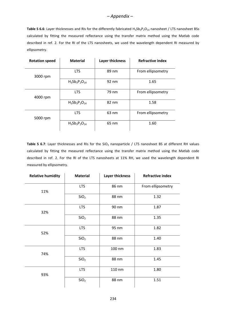
– Appendix –
234
Table S 6.6: Layer thicknesses and RIs for the differently fabricated H3Sb3P2O14 nanosheet / LTS nanosheet BSs
calculated by fitting the measured reflectance using the transfer matrix method using the Matlab code
described in ref. 2. For the RI of the LTS nanosheets, we used the wavelength dependent RI measured by
ellipsometry.
Rotation speed Material Layer thickness Refractive index
3000 rpm LTS 89 nm From ellipsometry
H3Sb3P2O14 92 nm 1.65
4000 rpm LTS 79 nm From ellipsometry
H3Sb3P2O14 82 nm 1.58
5000 rpm LTS 63 nm From ellipsometry
H3Sb3P2O14 65 nm 1.60
Table S 6.7: Layer thicknesses and RIs for the SiO2 nanoparticle / LTS nanosheet BS at different RH values
calculated by fitting the measured reflectance using the transfer matrix method using the Matlab code
described in ref. 2. For the RI of the LTS nanosheets at 11% RH, we used the wavelength dependent RI
measured by ellipsometry.
Relative humidity Material Layer thickness Refractive index
11% LTS 86 nm From ellipsometry
SiO2 88 nm 1.32
32% LTS 90 nm 1.87
SiO2 88 nm 1.35
52% LTS 95 nm 1.82
SiO2 88 nm 1.40
74% LTS 100 nm 1.83
SiO2 88 nm 1.45
93% LTS 110 nm 1.80
SiO2 88 nm 1.51
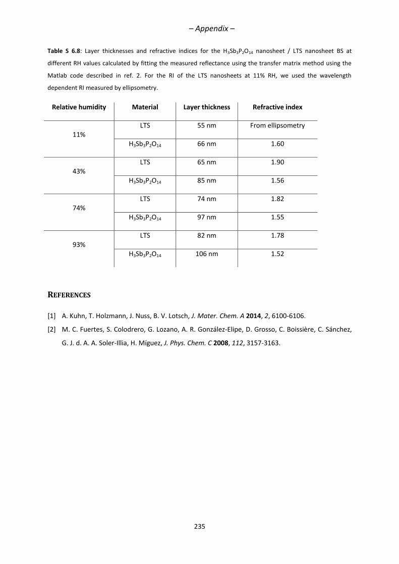
– Appendix –
235
Table S 6.8: Layer thicknesses and refractive indices for the H3Sb3P2O14 nanosheet / LTS nanosheet BS at
different RH values calculated by fitting the measured reflectance using the transfer matrix method using the
Matlab code described in ref. 2. For the RI of the LTS nanosheets at 11% RH, we used the wavelength
dependent RI measured by ellipsometry.
Relative humidity Material Layer thickness Refractive index
11% LTS 55 nm From ellipsometry
H3Sb3P2O14 66 nm 1.60
43% LTS 65 nm 1.90
H3Sb3P2O14 85 nm 1.56
74% LTS 74 nm 1.82
H3Sb3P2O14 97 nm 1.55
93% LTS 82 nm 1.78
H3Sb3P2O14 106 nm 1.52
REFERENCES
[1] A. Kuhn, T. Holzmann, J. Nuss, B. V. Lotsch, J. Mater. Chem. A 2014, 2, 6100-6106.
[2] M. C. Fuertes, S. Colodrero, G. Lozano, A. R. González-Elipe, D. Grosso, C. Boissière, C. Sánchez,
G. J. d. A. A. Soler-Illia, H. Míguez, J. Phys. Chem. C 2008, 112, 3157-3163.
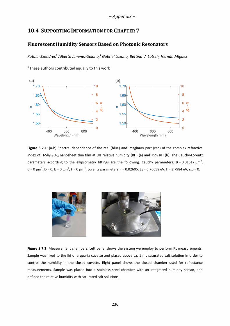
– Appendix –
236
10.4 SUPPORTING INFORMATION FOR CHAPTER 7
Fluorescent Humidity Sensors Based on Photonic Resonators
Katalin Szendrei,§ Alberto Jiménez-Solano,§ Gabriel Lozano, Bettina V. Lotsch, Hernán Míguez
§ These authors contributed equally to this work
Figure S 7.1: (a-b) Spectral dependence of the real (blue) and imaginary part (red) of the complex refractive
index of H3Sb2P2O14 nanosheet thin film at 0% relative humidity (RH) (a) and 75% RH (b). The Cauchy-Lorentz
parameters according to the ellipsometry fittings are the following. Cauchy parameters: B = 0.01617 μm2,
C = 0 μm4, D = 0, E = 0 μm
2, F = 0 μm
4; Lorentz parameters: f = 0.02605, E0 = 6.76658 eV, Γ = 3.7984 eV, εinf = 0.
Figure S 7.2: Measurement chambers. Left panel shows the system we employ to perform PL measurements.
Sample was fixed to the lid of a quartz cuvette and placed above ca. 1 mL saturated salt solution in order to
control the humidity in the closed cuvette. Right panel shows the closed chamber used for reflectance
measurements. Sample was placed into a stainless steel chamber with an integrated humidity sensor, and
defined the relative humidity with saturated salt solutions.
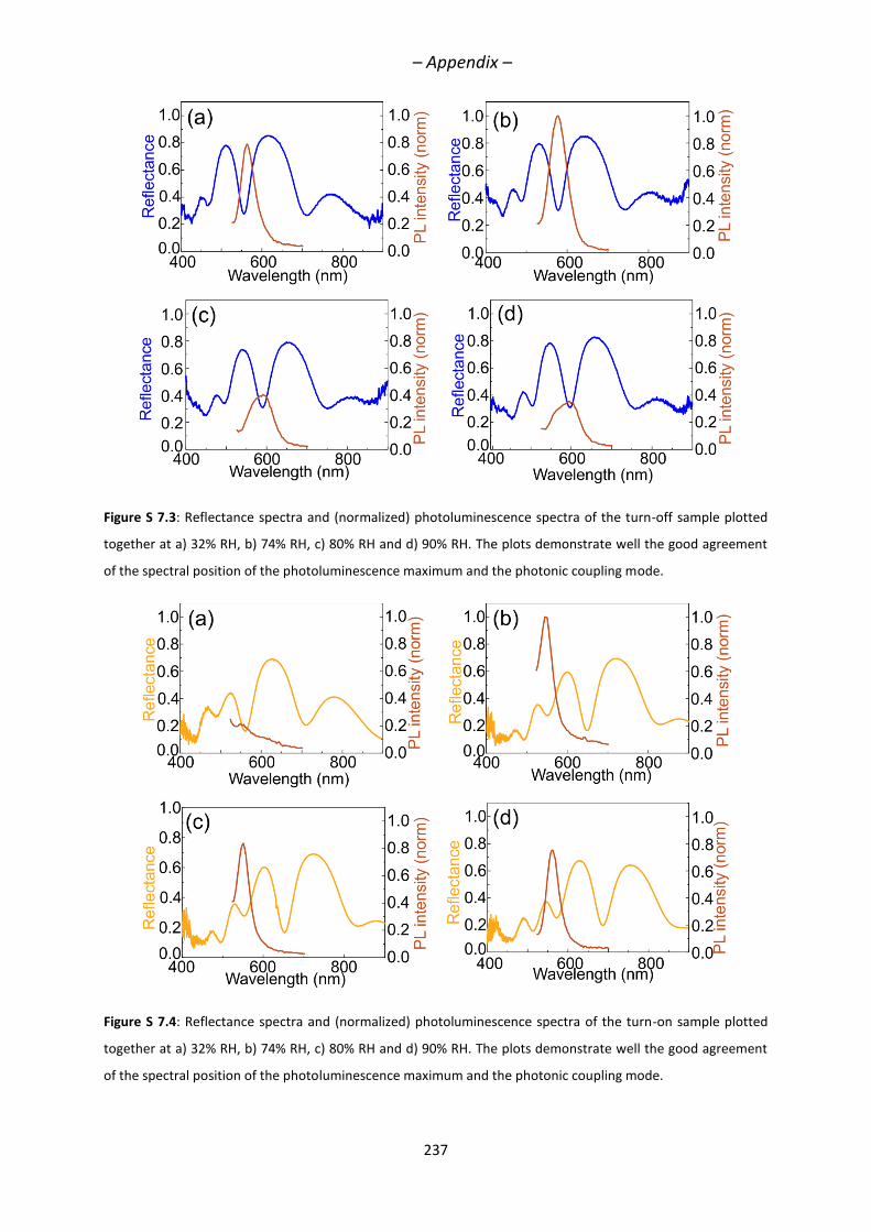
– Appendix –
237
Figure S 7.3: Reflectance spectra and (normalized) photoluminescence spectra of the turn-off sample plotted
together at a) 32% RH, b) 74% RH, c) 80% RH and d) 90% RH. The plots demonstrate well the good agreement
of the spectral position of the photoluminescence maximum and the photonic coupling mode.
Figure S 7.4: Reflectance spectra and (normalized) photoluminescence spectra of the turn-on sample plotted
together at a) 32% RH, b) 74% RH, c) 80% RH and d) 90% RH. The plots demonstrate well the good agreement
of the spectral position of the photoluminescence maximum and the photonic coupling mode.
– Appendix –
238
10.5 SUPPORTING INFORMATION FOR CHAPTER 8
Tracking Vertical Molecular Diffusion Into 1-dimensional Photonic Crystals
Katalin Szendrei-Temesi,§ Alberto Jiménez-Solano,§ Bettina V. Lotsch
§ These authors contributed equally to this work
EXPERIMENTAL SECTION
1DPC Fabrication
Multilayered structures consisting of alternate H3Sb3P2O14 nanosheets and TiO2 thin films were
fabricated following the spin-coating process previously described.[1] H3Sb3P2O14 nanosheets and TiO2
nanoparticles were synthesized according to the literature.[1-3] In total, we deposited 11 layers, as
first and last layer served TiO2. All 1DPCs were designed to exhibit the reflectance maximum in the
blue spectral range (≈ 450 nm), that the entire intercalation process for all amines in study is
detectable in the visible spectral range.
Diffusion Experiments
All amines, which were intercalated into the layered structures, were diluted to 1 M with ethanol in
order to ensure a similar evaporation rate and to keep the experimental conditions similar. 1 mL of
the amine solution was filled into a glass Petri dish with a volume of 20 cm³. Secondly, a 1 mm thick
acrylic glass plate with a round opening of 2 mm diameter was placed on top of the Petri dish
(Figure 1d). This acrylic glass plate serves as a lid of the chamber and the hole helps to spatially limit
the space, where the amine solution can evaporate from the chamber. The 1DPC was directly placed
on top of the acrylic glass and the optical measurements were carried out directly above the hole,
while the 1DPC was exposed directly to the amine vapor. The spectra were collected at normal
incident from a 1 mm spot with an spectrophotometer (Ocean Optics, USB2000+) attached to a
microscope (Leica, DM2500). With a smaller observation area compared to the diffusion hole, it
could be ensured that the whole sample area under study was exposed to the amine vapour equally.
This measurement set-up is summarized in Figure 1d. For all three amine intercalation experiments,
different areas of the same sample were used in order to minimize the structural fabrication
deviations between different samples.
Structural Characterization
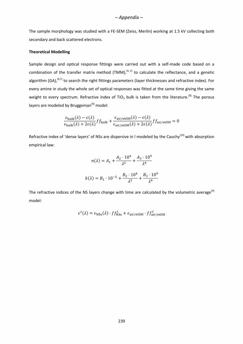
– Appendix –
239
The sample morphology was studied with a FE-SEM (Zeiss, Merlin) working at 1.5 kV collecting both
secondary and back scattered electrons.
Theoretical Modelling
Sample design and optical response fittings were carried out with a self-made code based on a
combination of the transfer matrix method (TMM),[4, 5] to calculate the reflectance, and a genetic
algorithm (GA),[6,7] to search the right fittings parameters (layer thicknesses and refractive index). For
every amine in study the whole set of optical responses was fitted at the same time giving the same
weight to every spectrum. Refractive index of TiO2 bulk is taken from the literature.[8] The porous
layers are modeled by Bruggeman[9] model:
Refractive index of ‘dense layers’ of NSs are dispersive in l modeled by the Cauchy[10] with absorption
empirical law:
The refractive indices of the NS layers change with time are calculated by the volumetric average[9]
model:
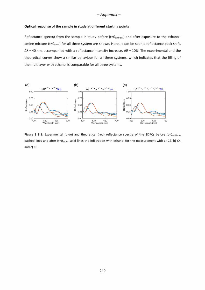
– Appendix –
240
Optical response of the sample in study at different starting points
Reflectance spectra from the sample in study before (t=0ambient) and after exposure to the ethanol-
amine mixture (t=0EtOH) for all three system are shown. Here, it can be seen a reflectance peak shift,
∆λ ≈ 40 nm, accompanied with a reflectance intensity increase, ∆R ≈ 10%. The experimental and the
theoretical curves show a similar behaviour for all three systems, which indicates that the filling of
the multilayer with ethanol is comparable for all three systems.
Figure S 8.1: Experimental (blue) and theoretical (red) reflectance spectra of the 1DPCs before (t=0ambient,
dashed lines and after (t=0EtOH, solid lines the infiltration with ethanol for the measurement with a) C2, b) C4
and c) C8.
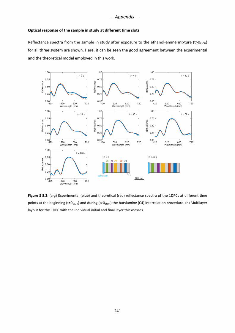
– Appendix –
241
Optical response of the sample in study at different time slots
Reflectance spectra from the sample in study after exposure to the ethanol-amine mixture (t>0EtOH)
for all three system are shown. Here, it can be seen the good agreement between the experimental
and the theoretical model employed in this work.
Figure S 8.2: (a-g) Experimental (blue) and theoretical (red) reflectance spectra of the 1DPCs at different time
points at the beginning (t=0EtOH) and during (t>0EtOH) the butylamine (C4) intercalation procedure. (h) Multilayer
layout for the 1DPC with the individual initial and final layer thicknesses.
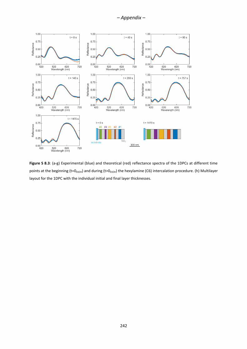
– Appendix –
242
Figure S 8.3: (a-g) Experimental (blue) and theoretical (red) reflectance spectra of the 1DPCs at different time
points at the beginning (t=0EtOH) and during (t>0EtOH) the hexylamine (C6) intercalation procedure. (h) Multilayer
layout for the 1DPC with the individual initial and final layer thicknesses.
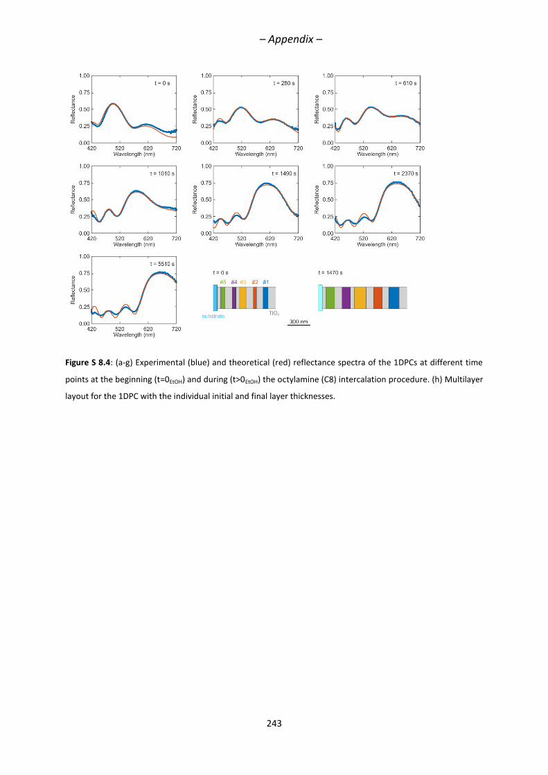
– Appendix –
243
Figure S 8.4: (a-g) Experimental (blue) and theoretical (red) reflectance spectra of the 1DPCs at different time
points at the beginning (t=0EtOH) and during (t>0EtOH) the octylamine (C8) intercalation procedure. (h) Multilayer
layout for the 1DPC with the individual initial and final layer thicknesses.
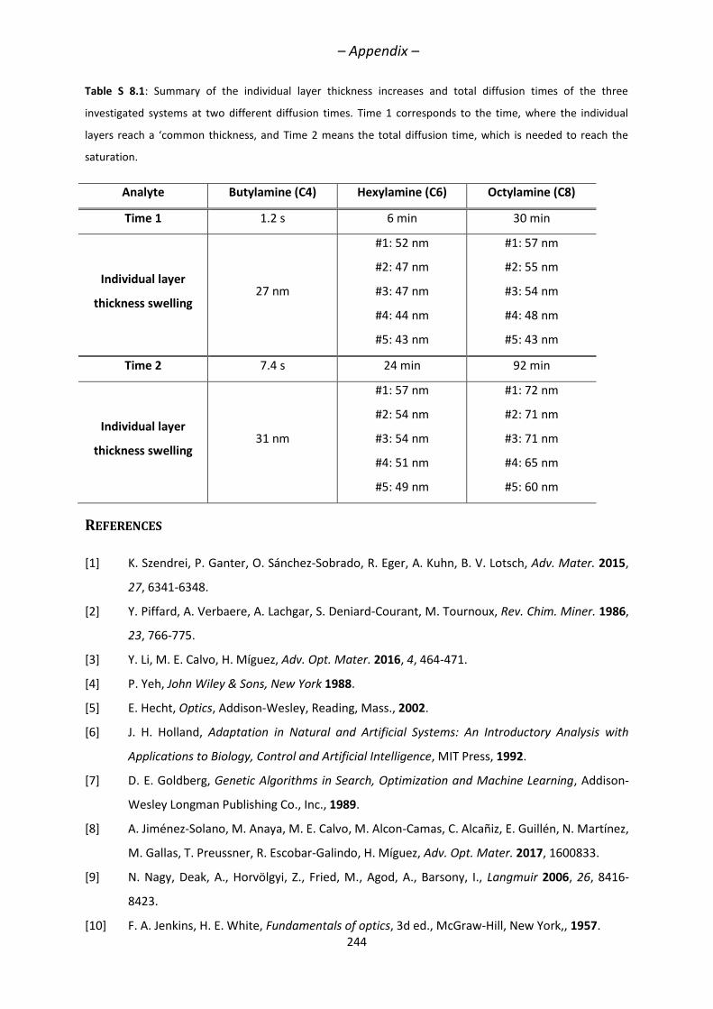
– Appendix –
244
Table S 8.1: Summary of the individual layer thickness increases and total diffusion times of the three
investigated systems at two different diffusion times. Time 1 corresponds to the time, where the individual
layers reach a ‘common thickness, and Time 2 means the total diffusion time, which is needed to reach the
saturation.
Analyte Butylamine (C4) Hexylamine (C6) Octylamine (C8)
Time 1 1.2 s 6 min 30 min
Individual layer
thickness swelling 27 nm
#1: 52 nm
#2: 47 nm
#3: 47 nm
#4: 44 nm
#5: 43 nm
#1: 57 nm
#2: 55 nm
#3: 54 nm
#4: 48 nm
#5: 43 nm
Time 2 7.4 s 24 min 92 min
Individual layer
thickness swelling 31 nm
#1: 57 nm
#2: 54 nm
#3: 54 nm
#4: 51 nm
#5: 49 nm
#1: 72 nm
#2: 71 nm
#3: 71 nm
#4: 65 nm
#5: 60 nm
REFERENCES
[1] K. Szendrei, P. Ganter, O. Sánchez-Sobrado, R. Eger, A. Kuhn, B. V. Lotsch, Adv. Mater. 2015,
27, 6341-6348.
[2] Y. Piffard, A. Verbaere, A. Lachgar, S. Deniard-Courant, M. Tournoux, Rev. Chim. Miner. 1986,
23, 766-775.
[3] Y. Li, M. E. Calvo, H. Míguez, Adv. Opt. Mater. 2016, 4, 464-471.
[4] P. Yeh, John Wiley & Sons, New York 1988.
[5] E. Hecht, Optics, Addison-Wesley, Reading, Mass., 2002.
[6] J. H. Holland, Adaptation in Natural and Artificial Systems: An Introductory Analysis with
Applications to Biology, Control and Artificial Intelligence, MIT Press, 1992.
[7] D. E. Goldberg, Genetic Algorithms in Search, Optimization and Machine Learning, Addison-
Wesley Longman Publishing Co., Inc., 1989.
[8] A. Jiménez-Solano, M. Anaya, M. E. Calvo, M. Alcon-Camas, C. Alcañiz, E. Guillén, N. Martínez,
M. Gallas, T. Preussner, R. Escobar-Galindo, H. Míguez, Adv. Opt. Mater. 2017, 1600833.
[9] N. Nagy, Deak, A., Horvölgyi, Z., Fried, M., Agod, A., Barsony, I., Langmuir 2006, 26, 8416-
8423.
[10] F. A. Jenkins, H. E. White, Fundamentals of optics, 3d ed., McGraw-Hill, New York,, 1957.
– Appendix –
245
10.6 LIST OF PUBLICATIONS
PUBLISHED AS A PART OF THIS THESIS
1. Touchless optical finger motion tracking based on 2D nanosheets with giant moisture
responsiveness, K. Szendrei*, P. Ganter*, O. Sánchez-Sobrado, R. Eger, A. Kuhn, B.V. Lotsch,
Adv. Mater. 2015, 27, 341-6348.
2. Towards the nanosheet-based photonic nose: Vapor recognition and trace water sensing
with antimony phosphate thin film devices, P. Ganter*, K. Szendrei*, B.V. Lotsch, Adv.
Mater. 2016, 28, 7436–7442., Inside front cover image.
3. Selectivity, cycling stability and temperature dependence of touchless finger motion
tracking devices based on 1D photonic crystal, K. Szendrei, P. Ganter, B.V. Lotsch, Proc. SPIE
9885, 2016, Photonic Crystal Materials and Devices XII, 98850Z.
4. Fluorescent photonic humidity sensors, K. Szendrei*, A. Jiménez-Solano*, G. Lozano, B. V.
Lotsch, H. Miguez, Adv. Optical Mater., 2017, 5, 1700663.
5. Lithium tin sulfide – a high-refractive-index 2D material for humidity-responsive Photonic
Crystals, K. Szendrei-Temesi, O. Sanchez-Sobrado, S. B. Betzler, K. M. Durner, T. Holzmann, B.
V. Lotsch, Adv. Func. Mater., 2018, 28, 1705740., Back cover image.
6. Tracking vertical molecular diffusion into 1-dimensional Photonic Crystals, K. Szendrei-
Temesi*, A. Jiménez-Solano*, B. V. Lotsch, 2018, to be submitted.
PATENTS
Gas and vapor sensing devices based on 2D nanosheet materials, K. Szendrei, P. Ganter, O.
Sanchez-Sobrado, A. Kuhn, B. V Lotsch, European Patent PCT/EP2015/07787, 2015.
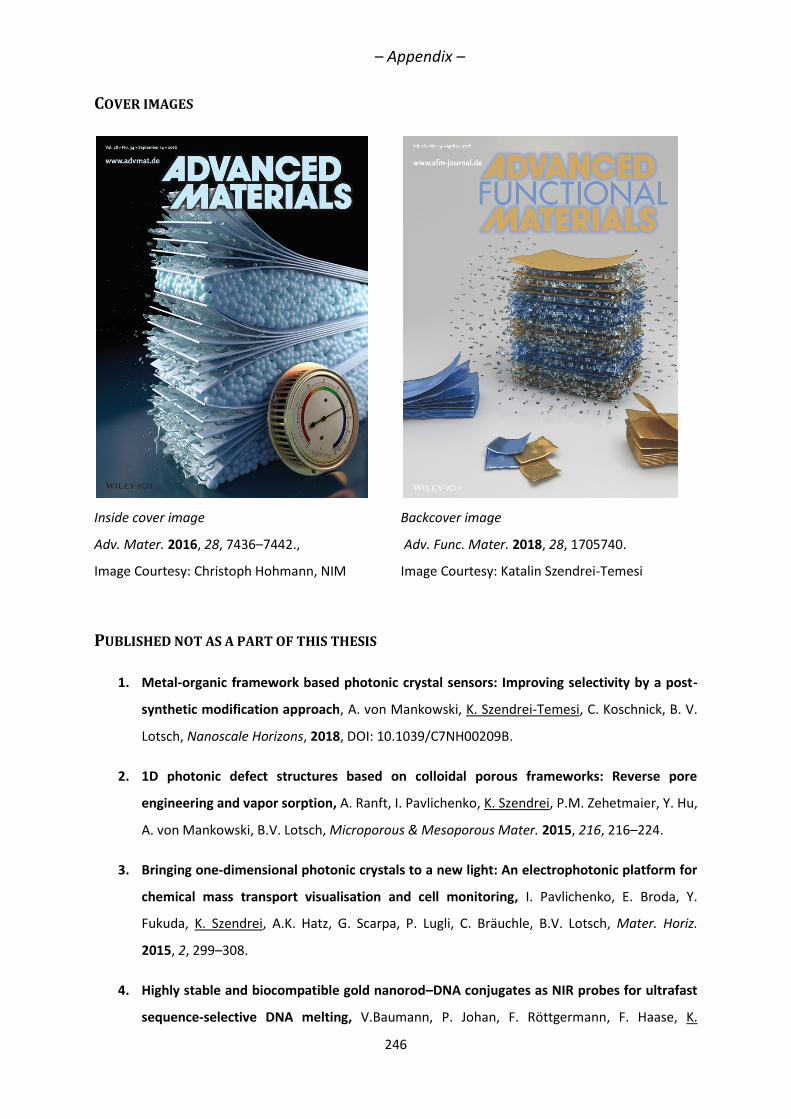
– Appendix –
246
COVER IMAGES
Inside cover image
Adv. Mater. 2016, 28, 7436–7442.,
Image Courtesy: Christoph Hohmann, NIM
Backcover image
Adv. Func. Mater. 2018, 28, 1705740.
Image Courtesy: Katalin Szendrei-Temesi
PUBLISHED NOT AS A PART OF THIS THESIS
1. Metal-organic framework based photonic crystal sensors: Improving selectivity by a post-
synthetic modification approach, A. von Mankowski, K. Szendrei-Temesi, C. Koschnick, B. V.
Lotsch, Nanoscale Horizons, 2018, DOI: 10.1039/C7NH00209B.
2. 1D photonic defect structures based on colloidal porous frameworks: Reverse pore
engineering and vapor sorption, A. Ranft, I. Pavlichenko, K. Szendrei, P.M. Zehetmaier, Y. Hu,
A. von Mankowski, B.V. Lotsch, Microporous & Mesoporous Mater. 2015, 216, 216–224.
3. Bringing one-dimensional photonic crystals to a new light: An electrophotonic platform for
chemical mass transport visualisation and cell monitoring, I. Pavlichenko, E. Broda, Y.
Fukuda, K. Szendrei, A.K. Hatz, G. Scarpa, P. Lugli, C. Bräuchle, B.V. Lotsch, Mater. Horiz.
2015, 2, 299–308.
4. Highly stable and biocompatible gold nanorod–DNA conjugates as NIR probes for ultrafast
sequence-selective DNA melting, V.Baumann, P. Johan, F. Röttgermann, F. Haase, K.
– Appendix –
247
Szendrei, P. Dey, K. Lyons, R. Wyrwich, M. Gräßel, J. Stehr, L. Ullerich, F. Bürsgens, J.
Rodríguez-Fernández, RSC Adv., 2016, 6,103724.
5. Use of electronic cigarettes (e-cigarettes) impairs indoor air quality and increases FeNO
levels of e-cigarette consumers, W. Schober, K. Szendrei, W. Matzen, H. Osiander-Fuchs, D.
Heitmann, T. Schettgen, R. A. Jörres, H. Fromme, Int. Journal of Hygiene and Environmental
Health, 2014, 217, 6, 628-637.
10.7 CONTRIBUTIONS TO CONFERENCES
ORAL PRESENTATIONS
April 17-21, 2017
Phoenix, USA
MRS Spring Meeting
K. Szendrei, P. Ganter, B. V. Lotsch
Touchless finger motion tracking with humidity sensitive 1D Photonic
Crystals
Silver Graduate Student Award
Februar 25, 2017
Harvard University,
Boston, USA
Boston Photonics Centennial Conference
K. Szendrei, P. Ganter, B. V. Lotsch
1D Photonic Crystals with ultrahigh humidity sensitivity
April 4-7, 2016
Brussels, Belgium
SPIE Photonics Europe
K. Szendrei, P. Ganter, B. V. Lotsch
Testing the selectivity, cycling stabilty and the temperature dependency of
touchless finger motion tracking devices based on 1D photonic crystals
Best Student Paper Award
March 6-11, 2016
Regensburg, Germany
DPG Spring Meeting
K. Szendrei, P. Ganter, B. V. Lotsch
Touchless finger motion tracking with humidity sensitive 1D Photonic
Crystals

– Appendix –
248
POSTER PRESENTATIONS
July 31-August 2, 2017
Hirschberg, Germany
NIM Summer retreat
K. Szendrei, O. Sanchez-Sobrado, S. Betzler, K. M. Durner, B. V. Lotsch,
Reflective and responsive – Li2Sn2S5 based 1D Photonic Crystals for novel
optical properties
Best Poster Award
July 27-29, 2016
Herrsching
NIM Summer retreat
K. Szendrei, P. Ganter, B. V. Lotsch
Touchless finger motion tracking with humidity sensitive 1D Photonic
Crystals
Best poster award
May 27-29, 2015
City University of
Hong Kong
CFP/NIM Workshop on Functional Photonics and Nanosystems
K. Szendrei, P. Ganter, O. Sanchez-Sobrado, R. Eger, A. Kuhn, B. V. Lotsch
2D nanosheet-based 1D Photonic Crystals with giant humidity
responsiveness
Nov 2015
Max Planck Institute
Stuttgart
Scientific Advisory Board Meeting of the Max Planck Institute for Solid
State Research
K. Szendrei, P. Ganter, O. Sanchez-Sobrado, R. Eger, A. Kuhn, B. V. Lotsch
2D nanosheet-based 1D Photonic Crystals with giant humidity
responsiveness
August 19-22, 2013
UCL London, UK
INASCON (International Nanoscience Conference) 2013
K. Szendrei, I. Pavlichenko, B. V. Lotsch
Towards miniature sensing platform: 1D Photonic Crystals in vapor and
solvent sensing applications
Best poster award
– Appendix –
249
10.8 CURRICULUM VITAE
EDUCATION
10/2014-Present
Max Planck Institute for Solid State Research and
Ludwig-Maximilians Universität, Munich
Group of Prof. Dr. Bettina V. Lotsch
PhD student
Research topic: 1D Photonic Crystals based on 2D nanosheet materials for
optical vapor sensing applications
Graduate School: Nanoinitiative Munich (NIM), student board member, 2017
10/2012-09/2014 Ludwig-Maximilians Universität, Munich
Master of Sciences in Chemistry
Master thesis – MPI for Solid State research, Group of Prof. Dr. Bettina Lotsch
1D Photonic Crystals based on 2D Nanosheet Materials as Optical Humidity
Sensors for Touchless Positioning Interfaces
10/2009-09/2012 Ludwig-Maximilians Universität, Munich
Bachelor of Sciences in Chemistry and Biochemistry
Bachelor thesis – LMU Munich, Group of Prof. Dr. Thomas Bein
Fluorocarbon surfactant mediated synthesis of mesoporous silica particles
and the influence of synthesis parameters
09/2004-06/2009 Kossuth Lajos Gimnázium, Budapest
High school
Bilingual Abitur
Awards and Scholarships
04/2017 Silver Graduate Student Award of the Material Research Society
04/2017 CeNS travel award
04/2016 Best Student Paper award of SPIE Photonics Europe
09-10/2015 Nanoinitiative Munich, Student Research Visit Award
10/2015 CeNS Publication Award
07/2016 and 08/2017 Best Poster award at the Summer Retreat of the Nanoinitiative Muich
08/2013 Best Poster Award at the INASCON Conference in London
06/2013 Lindau Nobel Laureate Meeting, Participation as a DAAD Scholarship holder
2009-2014 DAAD Scholarship for international high school students

250
„Look up at the stars and not down at your feet. Try to make sense of what
you see, and wonder about what makes the universe exist. Be curious.”
Stephen Hawking