vo2 nanosheets: controlling the thz properties through strain engineering
TRANSCRIPT
VO2 nanosheets: controlling the THz properties through strain engineering
Elsa Abreu§,1 Mengkun Liu§,1 Jiwei Lu§,2 Kevin G. West,2 Salinporn
Kittiwatanakul,3 Wenjing Yin,2 Stuart A. Wolf,3, 2 and Richard D. Averitt1
1Department of Physics, Boston University, Boston MA 02215, USA2Department of Materials Science and Engineering,
University of Virginia, Charlottesville VA 22904, USA3Department of Physics, University of Virginia, Charlottesville VA 22904, USA
We investigate far-infrared properties of strain engineered vanadium dioxide nanosheets throughepitaxial growth on a (100)R TiO2 substrate. The nanosheets exhibit large uniaxial strain leading tohighly uniform and oriented cracks along the rutile c-axis. Dramatic anisotropy arises for both themetal-insulator transition temperature, which is different from the structural transition temperaturealong the cR axis, and the metallic state conductivity. Detailed analysis reveals a Mott-Hubbardlike behavior along the rutile cR axis.§contributed equally to this work
arX
iv:1
112.
1573
v1 [
cond
-mat
.str
-el]
7 D
ec 2
011

2
I. INTRODUCTION
During the past five decades, vanadates have been intensely investigated from the point of view of clarifyingthe physics of metal-insulator transitions (MIT). Vanadium dioxide (VO2) is particularly intriguing, exhibiting aMIT with a conductivity decrease of over five orders of magnitude1. This is accompanied by a transition from ahigh temperature metallic rutile structure to an insulating monoclinic structure below the transition temperature.In bulk, the structural transition temperature, T bulkSt , equals the metal-insulator transition temperature, T bulkMI , i.e.T bulkSt ' T bulkMI ' 340K2. However, VO2 is not yet fully understood regarding the Mott-Hubbard or Peierls like natureof its MIT, though it is now generally accepted that a complete description requires explicit consideration of electron-electron correlations3,4. This is motivated in particular by the observed difference between the MIT and the structuraltransition temperatures, which provides significant evidence that the correlated conductivity behavior is independentof the structural phase5–7. Additionally, recent experimental studies highlight the multifunctional potential of VO2
including current or photoinduced phase changes (with the commensurate large tuning of the dielectric function) as wellas integration with other technologies for applications including light detection and memory-based metamaterials8–10.
Strain engineering enables an additional degree of control of technologically relevant properties and provides adiscriminatory capability towards obtaining fundamental insight into the microscopic origin of the macroscopic char-acteristics. Strain has been used to modify the MIT temperature in VO2 through direct application11 or substrate-dependent application12,13 of stress. For the present measurements, we utilize highly strained epitaxial (100)R VO2
thin films. The far-infrared conductivity is measured using non-contact polarization sensitive terahertz time-domainspectroscopy (THz-TDS) providing direct access to the coherent quasiparticle response along bR or cR by simplychanging the sample orientation. Subsequent analysis indicates that the strain engineered tuning of vanadium a1gand eπg orbitals controls the MIT transition temperature along cR, which is different from the structural transitiontemperature. The origin of the observed conductivity anisotropy is also discussed, along with the potential for atechnological application of strain engineered VO2 thin films as temperature switched far-infrared polarizers.
II. EXPERIMENTS
The ∼ 100nm and ∼ 250nm thick VO2 films we investigated were deposited on rutile (100)R TiO2 substrates bytemperature optimized sputtering from a vanadium target, using the reactive bias target ion beam deposition techniquein an Ar+O2 gas mixture; details of the growth conditions can be found elsewhere14. The samples morphology wascharacterized by optical, atomic force (AFM) and scanning electron microscopies (SEM), and the film microsctructurewas analyzed by temperature dependent X-ray diffraction (XRD).
THz-TDS is a non-contact method to measure far-infrared conductivity. The conductivity anisotropy is easilydetermined from transmission of THz pulses for different sample orientations. In our case the output of a 1kHz 35fsTi:Sapphire amplifier is used to generate nearly single-cycle THz pulses via optical rectification in a ZnTe crystal. Wethen employ a standard THz Time Domain Spectroscopy (THz TDS) setup to measure the transmission in the THzfrequency range ∼ 0.2 − 2.0THz15. By changing the sample orientation with respect to the THz pulse polarizationwe are able to monitor the transmission along different crystal axes.
(100)R TiO2 has a large refractive index anisotropy in the THz range, partly caused by its characteristic rutilestructure. Such an anisotropy in the (100)R TiO2 substrate makes it easy to distinguish transmitted THz signalswith polarization parallel to cR from THz signals with polarization perpendicular to bR (Fig. 1(a)). Temperaturedependent experimental characterization of the TiO2 substrate in the THz range, using our THz TDS setup, led tovalues of
ne ' 12.4− 6× 10⁻⁴∆T + 1.2i
no ' 9.1− 3× 10⁻⁴∆T + 0.4i
for the refractive index along cR and bR, respectively, in accordance with previous results16. Here, ∆T stands forthe temperature deviation with respect to room temperature. This approximation to the TiO2 complex refractiveindex holds between room temperature and 400K; it does not take into account the temperature dependence of theimaginary part, which is negligible for our purposes.
The conductivity of the VO2 film is extracted using the Fresnel equations, after experimental determination of theratio of the THz transmission of the film to the THz transmission of a bare TiO2 substrate, used as a reference.THz TDS is thus a non-contact conductivity measurement, which allows one to quickly characterize the conductivityanisotropy in many samples with different thicknesses and substrates.
III. RESULTS
A. Characterization of the VO2 nanosheets
3
Figure 2(a) is an AFM phase image of the 250nm film, showing periodic buckling and cracking of the film parallelto cR, with inter-crack spacings on the order of 1µm. The depth profile reveals nanosized ridges, ∼ 15nm high, nearthe cracks. The SEM image in Fig. 2(b) confirms the ∼ 250nm thickness of the film. It shows that the cracks’ depthmatches the film thickness and it gives an estimate of about 30nm for their width. Such nanocracks were not detectedby the AFM due to lack of tip sensitivity.
The optical images of the 100nm (Fig. 3(a)) and the 250nm (Fig. 3(b)) films confirm the ∼ 1µm period spacingof the cracks along cR. Also, the observed uniformity in the distribution of cracks is an indication that our films arestrained in a highly homogeneous and oriented fashion. This crack distribution enables a comparison of our resultswith those of VO2 nanobeams, aligned along cR
13,17–20, although the dimensionality of our nanosheets gives accessto the properties of strained VO2 along more than one axis. Such cracking uniformity was achieved by optimizingthe growth conditions of the samples, in particular the growth temperature. In the case of our (100)R VO2 films thegrowth temperature was set to ∼ 500C. Films grown at ∼ 450C show cracking along different directions, whichmakes the characterization of the films along cR less straightforward. All subsequent analysis is analogous for boththe 100nm and the 250nm thick films. Unless otherwise specified the results will refer to the 100nm thick sample.
Detailed room temperature XRD of the VO2 film confirms the single crystal nature of the sample and yields thelattice parameters of the material (Fig. 4(a)). Comparing these values with those in the rutile phase of bulk VO2
21
yields mismatches of −0.83% along aR, −2.17% along bR, and 1.41% along cR, indicative of a compressive strain alongaR and bR, as opposed to a tensile strain along cR. Such strain values along cR are comparable to those achievedin one-dimensional VO2 nanobeams17. Bulk rutile TiO2 has larger lattice constants than bulk rutile VO2 along alldirections so one would expect that both bR and cR would expand in (100)R VO2 films grown on a (100)R TiO2
substrate. However, our nanosheets show that the expansion along cR surpasses the substrate clamping effect due tothe bR-axis, leading to a compressive strain in the abR-plane. This behavior is also observed in the 250nm thick film,with mismatches of −0.68% along a250nmR , −1.94% along b250nm
R and 0.86% along c250nmR .Temperature dependent XRD results (Fig. 3(c)) show that a small aR-axis expansion, ∼ 0.1%, occurs during the
film’s structural transition. This transition occurs at a temperature T filmSt ∼ 340K ∼ T bulkSt , the same as in bulk,and shows the expected hysteric behavior. (From here on TSt will refer to both bulk and film structural transitiontemperatures.) The aR-axis expansion in our strained sheet can be compared to that in bulk VO2, estimated asaR−bMbM
' 0.6− 0.8%2,22, where bM is the equivalent of aR in the bulk monoclinic insulating structure. The order ofmagnitude difference between the lattice parameter variation in the film and that in bulk stems from the clampingeffect of the rutile TiO2 substrate. This is consistent with the large strain observed in room temperature XRD, causedby the strong substrate clamping effect. The structural change exhibited at 340K by our strained VO2 nanosheets isthus smaller than the change observed in bulk VO2. Since VO2 shares the TiO2 rutile structure at high temperatures,the reduced structural change is expected to have an impact mainly on the low temperature VO2 film’s structure.The temperature dependent (200)R 2θ plots from which the data in Fig. 3(c) were extracted are presented in Fig.4(b). These raw data provide further support to our observation that the clamping effect due to the substrate is verystrong, thereby preventing the development of significantly different structural phases in the strained VO2 film.
B. THz Time Domain Spectroscopy
As shown in Fig. 1, upon increasing the temperature from the insulating to the metallic phase the THz peaktransmission in the 100nm (100)R VO2 film drops by ∼70% along the cR-axis and by ∼15% along the bR-axis,and the THz peak transmission in the 250nm (100)R VO2 film drops by ∼85% along the cR-axis and by ∼15%along the bR-axis. Figure 1(b) shows the transmission anisotropy in our 250nm VO2 sample, normalized to its lowtemperature value along each axis (bR and cR). This representation highlights the dramatic difference between thelow temperature transmission along bR and that along cR, thereby illustrating the potential of strained VO2 films astemperature tunable THz polarizing beamsplitters.
Figure 5(a) shows the temperature dependent far infrared conductivity, obtained from the transmission data, forthe 100nm (100)R VO2 nanosheet. The conductivity along cR shows a clear transition from the insulating to themetallic state with a narrow hysteresis, which is indicative of the high quality of the film. In the metallic statethe conductivity is σcR ∼ 5650(Ωcm)−1, comparable to bulk single crystal values1. The MIT along cR occurs ata temperature T cRMI ' 365K. T cRMI is significantly larger than both the structural transition temperature and thebulk MIT temperature, TSt ∼ T bulkMI ∼ 340K. Our VO2 films therefore exhibit, along cR, a ∼ 25K temperaturedifference between the structural and the metal-insulator transition temperatures. The combination of the quasithree dimensionality of our nanosheets, which enables a direct measurement of the strain along the three crystal axesthrough XRD analysis, with the polarization sensitivity of THz spectroscopy is the key to identifying this distinctionbetween the two transition temperatures.
The conductivity along bR also exhibits a transition (see inset of Fig. 5(a)), which occurs at T bRMI ' 340K. Alongthis direction we therefore observe that the structural and metal-insulator transition temperatures are the same,T bRMI ∼ TSt ∼ T bulkMI . However, the conductivity along bR reaches a high temperature value about 30 times smaller

4
than the high temperature conductivity along cR. This strong conductivity anisotropy will be addressed later in thetext.
THz TDS results for the 250nm thick sample (Fig. 6) indicate that its transport properties are similar to that ofthe 100nm sample. In particular, the high temperature conductivity along cR remains as good as in bulk VO2 singlecrystals1 while T cRMI ' 365K > T bulkMI . The high temperature conductivity along bR is very low, < 100(Ωcm)−1, and
the transition temperature can only be estimated at T bRMI ' 340K, consistent with T bulkMI and TSt and in line withwhat is observed in the 100nm sample (Fig. 5(a)).
IV. DISCUSSION
Understanding the contribution of the V3d orbitals to the electronic properties is crucial in order to explain the largematerial anisotropy in TMI
23. A splitting of the 5-fold degenerate 3d states occurs due to the octahedral coordinationof the V atoms, resulting in a higher energy doubly degenerate eg level and a lower energy triply degenerate t2glevel. Trigonal distortion further splits the t2g levels leading to an upshifted doubly degenerate eπg state, responsiblefor conduction in the abR-plane, while downshifting a non-degenerate cR-oriented a1g state (Fig. 5(b)). Recentcluster Dynamical Mean Field Theory (cDMFT) calculations4, which include the effect of a ±2% strain along cR,have demonstrated that a tensile strain along cR narrows the a1g derived band and leads to a compressive strain inthe abR-plane, which uplifts the eπg band (Fig. 5(c)). In the Mott picture the energy increase of eπg electrons reducesthe screening of electrons residing in the a1g band, thereby enhancing the effect of correlations (i.e. increasing thescreened Hubbard U). This results in an increase of the insulating band gap which opens, below TMI , between thebonding a1g and the anti-bonding eπg levels, therefore leading to an increased TMI along cR.24,25.
The epitaxial strain in our film can be decomposed into a uniaxial tensile strain along cR and a uniaxial compressivestrain along bR. Along cR, T cRMI ∼ 365K > T bulkMI , in line with previous experimental results11, while σcR remainscomparable to the best single crystal values1. These results agree with the Mott picture above, where the increasedlattice spacing along cR further increases the ratio of Coulomb repulsion to the inter-atomic hopping integral, therebydestabilizing the metallic phase and increasing T cRMI . The Peierls picture predicts a decrease in T cRMI with tensile strainalong cR, thus failing to describe our results along that axis4. Also contrary to the Peierls-driven MIT scenario alongcR is the fact that the structural transition occurs at a temperature TSt ∼ 340K, 25K lower than T cRMI : in a Peierlspicture both transitions would be expected to occur at the same temperature. In contrast to what happens along cR,the results along bR, where T bRMI = TSt, are compatible with a Peierls-driven MIT scenario.
As mentioned above, our samples are cracked along cR. The occurrence of such cracks is common in VO2, in bothbulk and strained samples26,27, and this has prevented accurate measurements of the DC conductivity in this materialin the direction perpendicular to cR. Hindered quasiparticle motion along bR due to the presence of cR orientedcracks is the most likely explanation for the reduced value of σbR in our films. However, a different scenario could
arise in the THz range. Due to the small value of the far-infrared carrier mean free path (∼ A28) compared to DC,the ∼ 1ps long THz field should be able to couple to the material along bR despite the cracks along cR. According tothis picture, the uniaxial compressive strain along bR would play a significant role in reducing σbR , compared to σcR ,
while keeping T bRMI = T bulkMI = TSt. Given the orbitals orientation, conductivity in the abR-plane is mediated by theeπg orbitals whose energy is controlled by the overlap between O2p and V3d orbitals24. Low conductivity behaviorin the compressed abR-plane for T > TMI would then arise from the eπg states being higher in energy than in theunstrained case, which reduces their overlap with the Fermi level (Fig. 5C). VO2 nanosheets that remain uncrackedwhile maintaining a high level of strain along bR must be investigated in order to clarify the role of the eπg orbitalson the high temperature value of σbR , thereby also clarifying the nature of the MIT along that axis.
Our strained VO2 films on a TiO2 substrate have been shown to enable the separation of the far-infrared signal’spolarization components both in time and intensity. The temperature dependent THz conductivity of strained VO2
nanosheets (Figs. 5(a) and 6) shows that incident light polarized parallel to bR is transmitted through VO2 atboth low and high temperatures, whereas incident light polarized parallel to cR is transmitted through VO2 at lowtemperatures but reflected at high temperatures. Our strained VO2 single crystal nanosheets can thus be thought ofas temperature switchable far-infrared polarizing beamsplitters.
V. PHASE DIAGRAM
Finally, it is interesting to map the strain of our film onto the VO2 phase diagram in Fig. 7, constructed based onpast studies of VO2 as a function of temperature, pressure17,29 and doping30–33. In general, it is not trivial to mapthe effect of doping onto that of pressure. This was initiated by Pouget et al., who found a one-to-one correspondencebetween Cr-doping and the application of uniaxial stress along [110]R
29,32. Other doping experiments tend to indicatethat doping ions with radii smaller than V4+ lead to an increase in TMI whereas those with larger radii have theopposite effect34. This is similar to what happens in V2O3, a canonical Mott insulator35.

5
Figure 7 compiles previous experimental results obtained on VO2 under different pressure17,29 and doping30–33
conditions. P = 0 corresponds to atmospheric pressure. The application of hydrostatic pressure1,40,41 cannot beeasily interpreted in terms of its influence on the conductivity nor on TMI along individual axes of the crystallinestructure, which corresponds to the main focus of our study. We therefore do not include hydrostatic pressure data inthe phase diagram of Fig. 7. The dashed white lines delimit the region of the phase diagram where uniaxial pressurewas applied along [001]R (up to 12kbar), both for compression (P < 0) and tension (P > 0), and along [110]R (upto ∼ 1.2kbar), only for compression (P > 0). Within the rectangle, the dashed red line represents T cRMI versus stressalong cR, [001]R, while the solid red line represents T cRMI versus stress in the abR-plane, [110]R. The dashed blacklines separate different insulating phases within the low temperature monoclinic phase. The dash-doted line betweenphases M2 and M4 is a conjecture30,33. Note that apart from the dashed red line, relative to stress along [001]R, allthe information in the diagram refers to stress along [110]R. The white oval indicates the phase space characteristic ofour (100)R VO2 samples. The uniaxial stress on our films along [110]R has been estimated, respectively for the 100nmand the 250nm samples, to ∼ 20.9kbar and ∼ 18.5kbar, based on the measured −2.32% and −2.06% mismatch along(110)R, and on a Young modulus of ∼ 900kbar42. These uniaxial stress values are higher than ever reported, to ourknowledge, for uniaxial stress on VO2.
The dependence of TMI on doping, studied in V1−xMxO2 compounds, can be approximately mapped onto itsdependence on applied pressure. Reduction of V4+ is achieved using M = Nb, Mo, W, Ta, Re, Ir, F, Ti, Os, Ru, Tc,etc., with formal charges of +4, +5 or +623,32,34,43–54. The effect on TMI is similar to that of negative (compressive)stress along [001]R, yielding dTMI/dx = −0.3 ∼ −28K/at.%M . Oxidation of V4+ is achieved using M = Cr, Al, Fe,Ga, Ge, Sn, Mn, Co, etc., with formal charges of +3 or +423,31–34,39,43,55–59. The effect on TMI is similar to that ofpositive (tensile) stress along [001]R, yielding dTMI/dx = 0 ∼ 13K/at.%M .
Our results, indicated by the white oval in the phase diagram of Fig. 7, are comparable to those of Everhart et al.,where an anisotropy of about two orders of magnitude is observed in the metallic phase of bulk VO2 single crystalsdoped with iron at 0.076%37. Our estimate of the stress puts our samples in a region of the phase diagram where TMI
increases with stress, and where a two phase behavior is expected above TMI . This is consistent with our observationof both insulating (T < T cRMI) and metallic (T > T cRMI) values of σcR in the same rutile structure, above TSt. Theindependence of the conductivity behavior from the structural phase has been reported before5–7, though relative tomonoclinic structures. As for the low temperature structure, M4 or rutile seem to be the most likely candidates,although we cannot distinguish between the two. M1, M2 and M3/T are all structurally too far from rutile20,30,31
to lead to the results shown in Fig. 3C, and they are located in different regions of the phase diagram, as seen inFig. 7. These observations, along with the strong conductivity anisotropy exhibited by our strained nanosheets, areindicative of a more complex behavior of VO2, beyond the currently accepted doping and strain dependence of itsstructural and transport properties (Fig. 7).
Coming back to the conductivity measured in our strained nanosheets, it is important to point out that itsanisotropy is unexpectedly large compared to previous experimental observations and theoretical calculations onVO2 samples12,36–39. The anisotropy in the DC conductivity,
σcR
σbRor
σcR
σaR, in undoped VO2 samples is generally >1 for
T < TMI but can take many different values for T > TMI (Table I). Differences in sample quality and stoichiometryas well as in conductivity measurement techniques surely affect the results, but variations in geometry and internalstrain / cracking are likely to also have an effect on the anisotropy of metallic VO2.
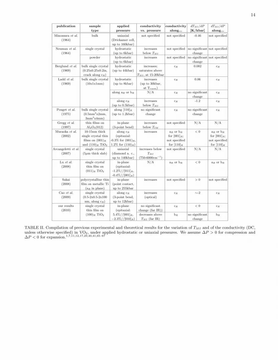
Tables I and II present a complete and up to date review, to our knowledge, of the experimental and theoretical dataon conductivity anisotropy in VO2, including the effect of externally applied stress. Table I includes the results forthe conductivity anisotropy, above and below TMI , when no external stress is applied12,36–39,60–64. Table II presentsseveral results for the strain induced variation of TMI and of the conductivity in VO2, for situations where hydrostaticor uniaxial pressure is applied to the samples1,7,11,12,17,29,40,41,65–67.
As seen in tables I and II, in most situations where uniaxial pressure is applied the conductivity is measured alongcR, the only axis along which it is well defined due to geometry constraints of the samples or to cracking. Few studiesdetermine the conductivity along aR or bR as a function of applied pressure. In general, it is agreed that (i) an applieduniaxial compressive (tensile) stress along the cR-axis leads to an increased (decreased) conductivity at T > TMI ;(ii) an applied uniaxial compressive (tensile) stress along the cR-axis leads to a decreased (increased) TMI (the axisalong which TMI is measured is not always specified); (iii) a small uniaxial stress applied along the [110]R directionhas no significant effect on the conductivity nor TMI along cR but it promotes a phase transition between differentmonoclinic structures (M1, M2, T/M3, M4), in the insulating phase29–31. Further experiments are needed in orderto systematically measure the conductivity along aR or bR under (i) an applied uniaxial stress along aR or bR; (ii)an applied uniaxial stress along cR; (iii) hydrostatic pressure. Also, clear criteria for distinguishing TMI from TStwould be extremely valuable to help draw a more accurate and complete phase diagram, in line with what has beenattempted in previous studies5–7. The highly oriented strain across a quasi three dimensional structure, achieved inepitaxially grown VO2 nanosheets, offers an extraordinary versatility and potential for investigation of these issues.
Theoretically, several pictures have been suggested to explain the anisotropy in (unstrained) VO2: (1) a two band

6
model description of 3d electrons, within the framework of the Goodenough model, predicts a non conducting abR-plane for T > TMI , any residual conductivity in that plane being due to the overlap of O2p and V3d orbitals23,24;(2) LDA calculations by Allen’s group predict the structural distortion to be the main force driving the MIT inVO2, following a simple Peierls picture68; (3) a three-band Hubbard model, suggested by Tanaka et al., predicts aone dimensional conducting phase along cR for T < TMI and an isotropically conducting phase for T > TMI
69; (4)LDA+cDMFT calculations by Biermann et al. suggest that electron correlations within the eπg levels are weaker than
those along the a1g ones3; (5) subsequent LDA+cDMFT calculations by Kotliar’s group, which include a moderatedegree of uniaxial strain, suggest that electronic correlations are the main driving force in the MIT, and that the rutilephase itself should be able to support both metallic and insulating electronic behavior4; (6) Liebsch et al. comparedthe LDA+U, DMFT and GW methods and found that none of them provides a full description of VO2, namely ofthe development of the insulating gap below TMI
70. Nonetheless, most of the calculations based on unstrained VO2
samples agree that (i) a1g and eπg states can be regarded as nearly independent; (ii) the conductivity is expected tobe of predominantly a1g behavior for T < TMI and nearly isotropic for T > TMI ; (iii) electron correlations shouldbe included in the model, mainly in the cR oriented a1g levels. Our results agree with (i) and (iii), while straininduced cracking prevents the accurate description of the effect mentioned in (ii). Further theoretical investigationsshould take into account not only strain4 but also the oxygen degrees of freedom, in order to provide a more accuratedescription of the O2p and V3d orbitals overlap, most relevant for describing the conductivity in the abR-plane,and of the subsequent cracking along cR. Such estimates would be adequate for a quantitative, rather than merelyqualitative, comparison with our experimental data.
VI. CONCLUSION
In summary, we have observed a large anisotropy of the properties of strained 100nm and 250nm thick VO2
nanosheets. The increased value of T cRMI compared to TSt is a clear signature of a Mott- rather than Peierls-drivenMIT along cR. An eπg orbital tuning picture is proposed to explain the reduced value of the high temperature σbR ,although a crack induced conductivity decrease cannot be conclusively ruled out. Additional experiments are neededin order to clarify the mechanism of the phase transition in strained VO2, mainly in the direction perpendicular tocR. This would allow the development of a more comprehensive phase diagram for this material. In general, epitaxialstrain engineering is a powerful tool which has the potential to enable careful tuning of the metal-insulator transitionin numerous other correlated electron materials, thereby providing a viable route towards technologically relevantmultifunctionality and increased understanding of the microscopic origin of the MIT.
ACKNOWLEDGMENTS
We thank Kebin Fan and Wei Zhang for SEM sample characterization. We acknowledge support from DOE - BasicEnergy Sciences under Grant No. DE-FG02-09ER46643 (E.A., M.L., R.D.A.). E. Abreu acknowledges support fromFundacao para a Ciencia e a Tecnologia, Portugal, through a doctoral degree fellowship (SFRH/ BD/ 47847/ 2008).
1 L. A. Ladd and W. Paul, Solid State Communications 7, 425 (1969)2 G. Andersson, Acta Chemica Scandinavica 10, 623 (1956)3 S. Biermann, A. Poteryaev, A. Lichtenstein, and A. Georges, Physical Review Letters 94, 026404 (Jan. 2005), ISSN 0031-
9007, http://link.aps.org/doi/10.1103/PhysRevLett.94.0264044 B. Lazarovits, K. Kim, K. Haule, and G. Kotliar, Physical Review B 81, 115117 (Mar. 2010), ISSN 1098-0121, http:
//link.aps.org/doi/10.1103/PhysRevB.81.1151175 H.-T. Kim, Y. W. Lee, B.-J. Kim, B.-G. Chae, S. J. Yun, K.-Y. Kang, K.-J. Han, K.-J. Yee, and Y.-S. Lim, Physical Review
Letters 97, 266401 (Dec. 2006), ISSN 0031-9007, http://link.aps.org/doi/10.1103/PhysRevLett.97.2664016 M. Qazilbash, A. Tripathi, A. Schafgans, B.-J. Kim, H.-T. Kim, Z. Cai, M. Holt, J. Maser, F. Keilmann, O. Shpyrko, and
D. Basov, Physical Review B 83, 165108 (Apr. 2011), ISSN 1098-0121, http://link.aps.org/doi/10.1103/PhysRevB.83.165108
7 E. Arcangeletti, L. Baldassarre, D. Di Castro, S. Lupi, L. Malavasi, C. Marini, A. Perucchi, and P. Postorino, PhysicalReview Letters 98, 196406 (May 2007), ISSN 0031-9007, http://link.aps.org/doi/10.1103/PhysRevLett.98.196406
8 H.-T. Kim, B.-G. Chae, D.-H. Youn, G. Kim, K.-Y. Kang, S.-J. Lee, K. Kim, and Y.-S. Lim, Applied Physics Letters 86,242101 (2005), ISSN 00036951, http://link.aip.org/link/APPLAB/v86/i24/p242101/s1&Agg=doi
9 T. Driscoll, H.-T. Kim, B.-G. Chae, B.-J. Kim, Y.-W. Lee, N. M. Jokerst, S. Palit, D. R. Smith, M. Di Ventra, and D. N.Basov, Science 325, 1518 (Sep. 2009), ISSN 1095-9203, http://www.ncbi.nlm.nih.gov/pubmed/19696311
10 D. Hilton, R. Prasankumar, S. Fourmaux, A. Cavalleri, D. Brassard, M. El Khakani, J. Kieffer, A. Taylor, and R. Averitt,Physical Review Letters 99, 226401 (Nov. 2007), ISSN 0031-9007, http://link.aps.org/doi/10.1103/PhysRevLett.99.226401
7
11 Y. Muraoka, Y. Ueda, and Z. Hiroi, Journal of Physics and Chemistry of Solids 63, 965 (Aug. 2002), ISSN 00223697,http://linkinghub.elsevier.com/retrieve/pii/S0022369702000987
12 J. Lu, K. G. West, and S. a. Wolf, Applied Physics Letters 93, 262107 (2008), ISSN 00036951, http://link.aip.org/link/APPLAB/v93/i26/p262107/s1&Agg=doi
13 S. Zhang, J. Y. Chou, and L. J. Lauhon, Nano Letters 9, 4527 (Dec. 2009), ISSN 1530-6992, http://www.ncbi.nlm.nih.gov/pubmed/19902918
14 K. G. West, J. Lu, J. Yu, D. Kirkwood, W. Chen, Y. Pei, J. Claassen, and S. a. Wolf, Journal of Vacuum Science &Technology A 26, 133 (2008), ISSN 07342101, http://link.aip.org/link/JVTAD6/v26/i1/p133/s1&Agg=doi
15 P. Jepsen, D. Cooke, and M. Koch, Laser & Photonics Reviews 5, 124 (Jan. 2011), ISSN 18638880, http://doi.wiley.com/10.1002/lpor.201000011
16 C. Jordens, M. Scheller, M. Wichmann, M. Mikulics, K. Wiesauer, and M. Koch, Applied optics 48, 2037 (Apr. 2009), ISSN1539-4522, http://www.ncbi.nlm.nih.gov/pubmed/19363540
17 J. Cao, E. Ertekin, V. Srinivasan, W. Fan, S. Huang, H. Zheng, J. W. L. Yim, D. R. Khanal, D. F. Ogletree, J. C.Grossman, and J. Wu, Nature Nanotechnology 4, 732 (Sep. 2009), ISSN 1748-3387, http://www.nature.com/doifinder/10.1038/nnano.2009.266
18 J. Wu, Q. Gu, B. S. Guiton, N. P. de Leon, L. Ouyang, and H. Park, Nano Letters 6, 2313 (Oct. 2006), ISSN 1530-6984,http://www.ncbi.nlm.nih.gov/pubmed/17034103
19 J. I. Sohn, H. J. Joo, D. Ahn, H. H. Lee, A. E. Porter, K. Kim, D. J. Kang, and M. E. Welland, Nano Letters 9, 3392 (Oct.2009), ISSN 1530-6992, http://www.ncbi.nlm.nih.gov/pubmed/19785429
20 A. C. Jones, S. Berweger, J. Wei, D. Cobden, and M. B. Raschke, Nano Letters 10, 1574 (May 2010), ISSN 1530-6992,http://www.ncbi.nlm.nih.gov/pubmed/20377237
21 D. B. McWhan, M. Marezio, J. P. Remeika, and P. D. Dernier, Physical Review B 10, 490 (1974)22 D. Kucharczyk and T. Niklewski, Journal of Applied Crystallography 12, 370 (1979)23 J. Goodenough, Journal of Solid State Chemistry 3, 490 (Nov. 1971), ISSN 00224596, http://linkinghub.elsevier.com/
retrieve/pii/002245967190091024 V. Eyert, Annalen der Physik (Leipzig) 11, 650 (Oct. 2002), ISSN 00033804, http://doi.wiley.com/10.1002/
1521-3889(200210)11:9<650::AID-ANDP650>3.0.CO;2-K25 A. Zylbersztejn and M. N. F., Physical Review B 11, 4383 (1975)26 C. N. Berglund and H. J. Guggenheim, Physical Review 185, 1022 (1969)27 K. Nagashima, T. Yanagida, H. Tanaka, and T. Kawai, Physical Review B 74, 172106 (Nov. 2006), ISSN 1098-0121,
http://link.aps.org/doi/10.1103/PhysRevB.74.17210628 M. Qazilbash, K. Burch, D. Whisler, D. Shrekenhamer, B. Chae, H. Kim, and D. Basov, Physical Review B 74, 205118
(Nov. 2006), ISSN 1098-0121, http://link.aps.org/doi/10.1103/PhysRevB.74.20511829 J. P. Pouget, H. Launois, J. P. D’Haenens, P. Merenda, and T. M. Rice, Physical Review Letters 35, 873 (1975)30 J. B. Goodenough and H. Y.-P. Hong, Physical Review B 8, 1323 (1973)31 M. Marezio, D. B. McWhan, J. P. Remeika, and P. D. Dernier, Physical Review B 5, 2541 (1972)32 J. P. Pouget and H. Launois, Journal de Physique Colloques 37, C4 (1976)33 P. Villeneuve, G., Drillon, M., Hagenmuller, Materials Research Bulletin 8, 1111 (1973)34 J. Macchesney and H. Guggenheim, Journal of Physics and Chemistry of Solids 30, 225 (Feb. 1969), ISSN 00223697,
http://linkinghub.elsevier.com/retrieve/pii/002236976990303535 D. B. McWhan, T. M. Rice, and J. P. Remeika, Physical Review Letters 23, 1384 (1969)36 H. J. Barker, A. S., Verleur, H. W., Guggenheim, Physical Review Letters 17, 1286 (1966)37 J. B. Everhart, C. R., MacChesney, Journal of Applied Physics 39, 2872 (1968)38 P. F. Bongers, Solid State Communications 3, 275 (1965)39 K. Kosuge, Journal of the Physical Society of Japan 22, 551 (1967)40 C. H. Neuman, A. W. Lawson, and R. F. Brown, The Journal of Chemical Physics 41, 1591 (1964)41 C. N. Berglund and A. Jayamaran, Physical Review 185, 1034 (1969)42 N. Sepulveda, A. Rua, R. Cabrera, and F. Fernandez, Applied Physics Letters 92, 191913 (2008), ISSN 00036951, http:
//link.aip.org/link/APPLAB/v92/i19/p191913/s1&Agg=doi43 F. Beteille and J. Livage, Journal of Sol-Gel Science and Technology 13, 915 (1998)44 G. Villeneuve, A. Bordet, A. Casalot, J. Pouget, H. Launois, and P. Lederer, Journal of Physics and Chemistry of Solids
33, 1953 (Jul. 1972), ISSN 00381098, http://linkinghub.elsevier.com/retrieve/pii/003810987291191X45 C. Piccirillo, R. Binions, and I. P. Parkin, European Journal of Inorganic Chemistry 2007, 4050 (Sep. 2007), ISSN 14341948,
http://doi.wiley.com/10.1002/ejic.20070028446 M. Horlin, T., Niklewski, T., Nygren, Materials Research Bulletin 8, 179 (1973)47 K. Holman, T. McQueen, A. Williams, T. Klimczuk, P. Stephens, H. Zandbergen, Q. Xu, F. Ronning, and R. Cava, Physical
Review B 79, 245114 (Jun. 2009), ISSN 1098-0121, http://link.aps.org/doi/10.1103/PhysRevB.79.24511448 M. Nygren, M., Israelsson, Materials Research Bulletin 4, 881 (1969)49 B. G. Chae, H. T. Kim, and S. J. Yun, Electrochemical and Solid-State Letters 11, D53 (2008), ISSN 10990062, http:
//link.aip.org/link/ESLEF6/v11/i6/pD53/s1&Agg=doi50 O. Savborg and M. Nygren, Physica Status Solidi (a) 43, 645 (Oct. 1977), ISSN 00318965, http://doi.wiley.com/10.
1002/pssa.221043023651 M. Bayard, Journal of Solid State Chemistry 12, 41 (Jan. 1975), ISSN 00224596, http://linkinghub.elsevier.com/
retrieve/pii/0022459675901760

8
52 I. K. Kristensen, Journal of Applied Physics 39, 5341 (1968)53 B.-O. Marinder and A. Magneli, Acta Chemica Scandinavica 11, 1635 (1957)54 Q. Gu, A. Falk, J. Wu, L. Ouyang, and H. Park, Nano Letters 7, 363 (Mar. 2007), ISSN 1530-6984, http://www.ncbi.nlm.
nih.gov/pubmed/1725691555 M. Drillon and G. Villeneuve, Materials Research Bulletin 9, 1199 (1974)56 E. Pollert, G. Villeneuve, F. Menil, and P. Hagenmuller, Materials Research Bulletin 11, 159 (1976)57 F. Pintchovski, W. S. Glaunsinger, and A. Navrotsky, Journal of the Physics and Chemistry of Solids 39, 941 (1978)58 I. Kitahiro and A. Watanabe, Japanese Journal of Applied Physics 6, 1023 (1967)59 M.-H. Lee, M.-G. Kim, and H.-K. Song, Thin Solid Films 290-291, 30 (1996)60 H. W. Verleur, A. S. Barker, and C. N. Berglund, Physical Review 172, 788 (1968)61 a. Continenza, S. Massidda, and M. Posternak, Physical Review B 60, 15699 (Dec. 1999), ISSN 0163-1829, http://link.
aps.org/doi/10.1103/PhysRevB.60.1569962 R. J. O. Mossanek and M. Abbate, Journal of Physics: Condensed Matter 19, 346225 (Aug. 2007), ISSN 0953-8984,
http://stacks.iop.org/0953-8984/19/i=34/a=346225?key=crossref.097329a8505cf348ca29f0117d3a15db63 S. Lysenko, V. Vikhnin, F. Fernandez, A. Rua, and H. Liu, Physical Review B 75, 075109 (Feb. 2007), ISSN 1098-0121,
http://link.aps.org/doi/10.1103/PhysRevB.75.07510964 J. Tomczak and S. Biermann, Physical Review B 80, 1 (Aug. 2009), ISSN 1098-0121, http://link.aps.org/doi/10.1103/
PhysRevB.80.08511765 S. Minomura and H. Hagasaki, Journal of the Physical Society of Japan 19, 131 (1964)66 J. M. Gregg and R. M. Bowman, Applied Physics Letters 71, 3649 (1997), ISSN 00036951, http://link.aip.org/link/
APPLAB/v71/i25/p3649/s1&Agg=doi67 J. Sakai, Journal of Applied Physics 104, 073703 (2008), ISSN 00218979, http://link.aip.org/link/JAPIAU/v104/i7/
p073703/s1&Agg=doi68 R. M. Wentzcovitch, W. W. Schulz, and P. B. Allen, Physical Review Letters 72, 3389 (1994)69 A. Tanaka, Journal of the Physics Society Japan 72, 2433 (Oct. 2003), ISSN 0031-9015, http://jpsj.ipap.jp/link?JPSJ/
72/2433/70 a. Liebsch, H. Ishida, and G. Bihlmayer, Physical Review B 71, 085109 (Feb. 2005), ISSN 1098-0121, http://link.aps.
org/doi/10.1103/PhysRevB.71.085109

9
// cR axis
// bR axis
4
-4-202
Tran
smis
sion
(a.u
.)
Time (ps)0-5 -2.5 2.5-7.5
-6-8
VO2, T>TIMTiO2, T<TIM
VO2, T<TIM
TiO2, T>TIM
1
-1
0
// bR axis // cR axis
0-5 -2.5 2.5-7.5Time (ps)
Tran
smis
sion
(a.u
.)
VO2, T>TIM
VO2, T<TIM
(a)
(b)
FIG. 1. (a) THz transmission along cR and bR (vertically offset) in the 100nm (100)R VO2 sample (solid) and in the TiO2
reference substrate (dashed), below (blue) and above (red) TMI . The large refractive index anisotropy of the TiO2 substrateleads to a slower propagation of the laser pulse along cR than along bR, which enables the distinction of the two signals, andthus the orientation of the sample with respect to the incident field polarization. (b) THz transmission along cR and bR in the250nm (100)R VO2 sample, below (blue) and above (red) TMI , normalized to the high temperature value. The relative lowtemperature transmission along bR (∼ 85%) is dramatically different from that along cR (∼ 15%).
FIG. 2. Characterization of the 250nm thick (100)R VO2 film. (a) AFM phase image (0-5 scale) and corresponding heightprofile: the 250nm sample shows buckling induced ridges along cR (height indicated by the arrows: ∆z = 14.307nm). (b) SEMimage of a section of the sample (seen from the edge, the surface and the cross section being located as labeled) showing a∼ 30nm wide crack.

10
0
0.1
0.2
305 325 345 365Temperature (K)
(200
) spa
cing
% c
hang
e
TiO2
VO2
(c)
cR axis
55μm
1.56μm
(b)(100nm VO2)
cR axis
1.19μm
4.05μm
55μm
(250nm VO2)
340μm
(250nm VO2)(a)
FIG. 3. Characterization of VO2 thin films on a (100)R TiO2 substrate. Optical images of the (a) 250nm and (b) 100nmfilms: the samples show buckling induced ridges along cR, spaced by ∼ 1µm. (c) Temperature dependence (for increasing anddecreasing temperature) of the a-axis lattice spacing, deduced from XRD data: a ∼ 0.1% increase is observed along aR, in the100nm thick VO2 sample, across the structural transition which occurs at TSt = 340K. The expected linear increase of theaR-axis lattice spacing of TiO2 with temperature is also observed.

11
300
310
320
330
340
350
360
Tem
pera
ture
(K)
2θ (degrees)40.039.539.0
min
38.53837.53736.53635.52θ (degrees)
VO2 (101)
TiO2 (101)
Inte
nsity
(a. u
.)
4039.5392θ (degrees)
TiO2 (200)
VO2 (200)
28.52827.5272θ (degrees)
VO2 (110)
TiO2 (110)(a)
(b)
FIG. 4. (a) Room temperature XRD of the 100nm thick VO2 thin film, along three different directions: (200)R, (110)R, (101)R.
The lattice parameters can be estimated as 4.52A along aR, 4.46A along bR and 2.89A along cR, yielding mismatches of −0.83%along aR, −2.17% along bR and 1.41% along cR. (b) Temperature dependent XRD of the 100nm thick VO2 thin film. Boththe TiO2 and the VO2 (200)R peaks are seen to shift as a function of temperature. There is no evidence of the developmentof any additional structural phase.
300 325 350 375 400 425Temperature (K)
Con
duct
ivity
(Ω-1
cm-1
)
Unstrained metal(isotropic)
aR bR
cR
(b) (c)
(a)
Strained metal(anisotropic)
egπ
a1g
egπ
EF
a1g
V O
6000
7000
0
1000
2000
3000
4000
5000
// cR, T down
// bR, T up// bR, T down// cR, T up
300 375350325
200150100
500σ
(Ω-1
cm-1
)
Temperature (K)
cR
bR
FIG. 5. (a) Temperature dependence of the far infrared conductivity in 100nm (100)R VO2: σcR ' 30σbR above the MIT
temperature; T cRMI = 365K while T bRMI = 340K = T bulkMI . (b) The VO2 rutile unit cell, following Eyert24. (c) Effect of tensilestrain along cR on the electronic structure of metallic VO2: antibonding eπg bands are shifted upwards while the a1g band isnarrowed.

12
300 320 340 360 380 400 420
01000
2000
3000
4000
5000
6000
7000
Temperature (K)
Con
duct
ivity
(Ω-1
cm-1
)
// cR, T down// cR, T up// bR, T up// bR, T down
300320340360380400
050
100150200
cR
σ(Ω
-1cm
Temperature (K)
bR)-1
FIG. 6. Temperature dependence of the far-infrared conductivity in 250nm (100)R VO2: σcR ' 5250(Ωcm)−1 for T > T cRMI '365K; σbR < 100(Ωcm)−1 and T bRMI can only be estimated as T bRMI ' 340K.
Tem
pera
ture
(K)
300
400
Tensile // [001]RCompressive // [110]R
0 0.03 0.06 0.09 0.18 0.210.030.060.090.12M = Nb5+
20 60 70-20-30
350
250
Stress (kbar)
M= Cr3+x
450
Compressive // [001]RTensile // [110]R
METAL
SEMICOND
TWOPHASE
II
SEMICONDUCTOR
UNKNOWN
M4
T,M3
R
M’ M1R’
R
M2
3010-10
TWOPHASE
I
FIG. 7. Phase diagram of VO2 for stress applied mostly along [110]. The black solid line indicates TMI ; the white oval definesthe phase space of our samples; uniaxial stress results are presented in the region delimited by the dashed white lines; doping(V1−xMxO2) leading to reduction (M=Nb5+) or oxidation (M=Cr3+) of V4+ is specified on the top horizontal axis17,29–33
(refer to the main text for more details).

13
publication sample type method anisotropy anisotropy
below TMI above TMI
Bongers et al. bulk single crystal two-probe 2 2.5
(1965) (needle along cR,
6x0.3x0.15mm)
Barker et al. bulk polycrystal Hall voltage 0.7-0.8 1.1-2
(1966) (well defined cR)
Kosuge et al. bulk single crystal two-probe 1.14 0.58
(1967)
Koide et al. single crystal film two probe 2 0.001-0.1
(1967) on rutile substrate
bulk single crystal two-probe < 1.2 0.33
(needle along cR,
3x0.8x0.07mm)
Everhart et al. bulk single crystal four-probe 2-10 7.5
(1968) (4-7x1-4x1-4mm)
Verleur et al. bulk single crystal reflectivity 0.28-1.4 0.79-2
(1968) (0.25-5eV )
Continenza et al. (calculations) model GW 3-6.7 N/A
(1999) (0-10eV )
Mossanek et al. (calculations) LDA (0-12eV ) 0.6-> 3 0.7-3.3
(2007)
Lysenko et al. 30nm film on optical (400nm) 1.05 1
(2007) (012) Al2O3 diffraction
Lu et al. 40nm film on star-shaped 5.14 1
(2008) (011)R TiO2 electrodes
Tomczak et al. (calculations) LDA+CDMFT 0.73-1.67 0.96-1.14
(2009) (0-5eV )
our results 100nm film on THz TDS N/A ∼30
(2010) (100)R TiO2 (far infrared)
TABLE I. Compilation of previous experimental and theoretical results for the conductivity (DC, unless otherwise specified)anisotropy,
σcRσbR
orσcRσaR
, in VO2, above and below TMI , when no external stress is applied.12,36–39,60–64
14
publication sample applied conductivity conductivity dTMI/dP dTMI/dP
type pressure vs. pressure along... [K/kbar] along...
Minomura et al. bulk uniaxial not specified not specified -0.46 not specified
(1964) (Drickamer cell,
up to 160kbar)
Neuman et al. single crystal hydrostatic increases not specified no significant not specified
(1964) (up to 6kbar) below TMI change
powder hydrostatic increases not specified no significant not specified
(up to 6kbar) change
Berglund et al. bulk single crystal hydrostatic increases; cR 0.082 cR(1969) (0.25x0.25x0.2in, (up to 44kbar) saturates above
crack along cR) TMI , at 15-20kbar
Ladd et al. bulk single crystal hydrostatic increases cR 0.06 cR(1969) (10x1x1mm) (up to 8kbar) (up to 30kbar,
at Troom)
along aR or bR N/A cR no significant cRchange
along cR increases cR -1.2 cR(up to 0.5kbar) below TMI
Pouget et al. bulk single crystal along [110]R no significant cR no significant cR(1975) (0.5mm2x2mm, (up to 1.2kbar) change change
3mm2x4mm)
Gregg et al. thin films on in-plane increases not specified N/A N/A
(1997) Al2O3(012) (3-point bend) below TIM
Muraoka et al. 10-15nm thick along cR increases aR or bR < 0 aR or bR(2002) single crystal thin (epitaxial: for [001]R; for [001]R;
films on (001)R -0.3% for (001)R, not specified not specified
and (110)R TiO2 1.2% for (110)R) for [110]R for [110]R
Arcangeletti et al. single crystal uniaxial increases below not specified N/A N/A
(2007) (5µm thick slab) (diamond a. c., TMI
up to 140kbar) (750-6000cm−1)
Lu et al. single crystal in-plane N/A aR or bR < 0 aR or bR(2008) thin film on (epitaxial:
(011)R TiO2 -1.2%//[011]R,
-0.4%//[001]R)
Sakai polycrystalline thin in-plane increases not specified > 0 not specified
(2008) film on metallic Ti (point contact,
(aR in plane) up to 255kbar
Cao et al. single crystal along cR increases cR ∼-2 cR(2009) (0.5-2x0.5-2x100 (3-point bend, (optical)
nm, along cR) up to 12kbar)
our results single crystal in-plane no significant cR < 0 cR(2010) thin film on (epitaxial: change (far IR))
(100)R TiO2 5.4%//[001]R, decreases above bR no significant bR−2.3%//[010]R) TMI (far IR) change
TABLE II. Compilation of previous experimental and theoretical results for the variation of TMI and of the conductivity (DC,unless otherwise specified) in VO2, under applied hydrostatic or uniaxial pressures. We assume ∆P > 0 for compression and∆P < 0 for expansion.1,7,11,12,17,29,40,41,65–67