division of eislab improved pwb test methodologies
TRANSCRIPT

LICENTIATE T H E S I S
Department of Computer Science, Electrical and Space EngineeringDivision of EISLAB
Improved PWB Test Methodologies
Abdelghani Renbi
ISSN: 1402-1757 ISBN 978-91-7439-536-5
Luleå University of Technology 2012
Abdelghani R
enbi Improved PW
B Test M
ethodologies
ISSN: 1402-1757 ISBN 978-91-7439-XXX-X Se i listan och fyll i siffror där kryssen är


Improved PWB Test Methodologies
Abdelghani Renbi
Dept. of Computer Science, Electrical and Space EngineeringLulea University of Technology
Lulea, Sweden
Supervisors:
Prof. Jerker Delsing and Dr. Jan van Deventer

Printed by Universitetstryckeriet, Luleå 2012
ISSN: 1402-1757 ISBN 978-91-7439-536-5
Luleå 2012
www.ltu.se

To my parents
iii

iv

Abstract
Printed Wiring Board (PWB) and Printed Circuit Board Assembly (PCBA) testing aimsto ensure an error free board after the etching and the assembly processes. After theetching process, several types of errors might occur such as opens and bridges, whichare already, showstoppers in Direct Current (DC) applications. Mouse bites, spurs andother errors such as weak traces, which can be problematic in Radio Frequency (RF)and high frequency applications. Loading expensive component on defective boards canbe economically catastrophic especially for high volume production. The rule of tenwhich has been reported by the production experts says that defect costs ten timeswhen detected in the next testing phase. Bare board also needs to be tested for thecharacteristic impedance correctness due to the process variations and the compoundingraw material tolerances that can cause characteristic impedance mismatches. Althoughtesting the characteristic impedance is not in interest in some application, sampling thecharacteristic impedance for a specific design is one way to test the manufacturing processstability for better tuning, otherwise PWBs might differ from each other even within thesame batch. In addition to the possibility of defective PWB, the assembly process isnever perfect to achieve 100 % of PCBA yield due to the possible errors in the processsteps such as paste application, pick and place operations and soldering process whichmight lead to bridges, opens, wrong or miss oriented components.
For low volume production, flying probes test technology is cost efficient as com-pared to bed-of-nails. The performance of the flying probes system depends on the testalgorithm, the mechanical speed and the number of probes. To reduce the initial andmaintenance costs of the probing technology and to accelerate the test time, Paper Aintroduces a new indirect method to test PWB continuity and isolation testing using asingle probe for testing both continuity and isolation at the same time. RF signal isinjected into the trace under test, instead of a DC current. The phase shift betweenthe incident and the reflected signals is measured as it carries the information about thecorrectness of the trace when compared with a reference value of the same trace in thecorrect board.
The method shown an important capability for detecting PWB defects such as asopens, DC and RF bridges and other defects that change the characteristic impedancesuch as different line width. The margin in the measurement between a defective and acorrect board, which depends on the type of the defect, is about 7 % to 68 %. Applyingthis approach to PCBA testing led to significant margins between correct and defectiveinterconnect. The test cases in paper C shown 40 % and 33 %. Moreover, this margin hasbeen proven to be important even for short microstrip line, which intended to connect
v

two typical IC pins. This technique is strongly recommended to be applied to PCBAtesting where probing is feasible. The approach can be applied to the complete layouttesting or to boost a test strategy whose test solutions are not covering 100 % of thepossible defects.
By applying this test solution to bed-of-nails equipment, only 50 % of the probeswill be required, on the other hand, for a given design with NI isolated traces and NAadjacent pairs, employing this solution to flying probes system with two probes, leadsto the reduction of the number of tests from (NI+NA) tests to NI tests as isolation andcontinuity are performed in one go. Flying probes system involves mechanical movements,which dominate the test time, reducing the mechanical movements increases dramaticallythe test throughput. On the other hand, the proposed test method is believed to beextremely fast to test the correctness of the characteristic impedance which is prone tovariations due to the instability of the PWB manufacturing process, in the same time onecould employ the method to evaluate the process stability by checking after each batchof PWBs. Paper B and D provide insight into the impact of the PWB manufacturingvariations on the characteristic impedance. Moreover single probe approach is believedto have a good potential for Sequential Build-Up (SBU) interconnects testing whereconnections between component pads and the upper layers are often impossible to testwith the current test technologies.
vi

ContentsPart I 1
Chapter 1 – Introduction 31.1 Testing . . . . . . . . . . . . . . . . . . . . . . . . . . . . . . . . . . . . 31.2 PWB and PCBA test motivations . . . . . . . . . . . . . . . . . . . . . . 41.3 Testability . . . . . . . . . . . . . . . . . . . . . . . . . . . . . . . . . . 41.4 Design for Testability (DfT) . . . . . . . . . . . . . . . . . . . . . . . . . 51.5 Research question and applied methodology . . . . . . . . . . . . . . . . 6
Chapter 2 – History 9
Chapter 3 – Product Realization Process 133.1 Product realization process . . . . . . . . . . . . . . . . . . . . . . . . . . 133.2 Testing types . . . . . . . . . . . . . . . . . . . . . . . . . . . . . . . . . 153.3 IPC-TM-650 . . . . . . . . . . . . . . . . . . . . . . . . . . . . . . . . . . 17
Chapter 4 – Test Challenges 194.1 PWB and PCBA evolutions . . . . . . . . . . . . . . . . . . . . . . . . . 194.2 Components diversity . . . . . . . . . . . . . . . . . . . . . . . . . . . . . 204.3 Rising clock speed . . . . . . . . . . . . . . . . . . . . . . . . . . . . . . . 204.4 Moore’s law . . . . . . . . . . . . . . . . . . . . . . . . . . . . . . . . . . 204.5 Sequential Build-Up . . . . . . . . . . . . . . . . . . . . . . . . . . . . . 21
Chapter 5 – PWB and PCBA Defects 235.1 Fault spectrum . . . . . . . . . . . . . . . . . . . . . . . . . . . . . . . . 235.2 PCBA defects . . . . . . . . . . . . . . . . . . . . . . . . . . . . . . . . . 235.3 PWB defects . . . . . . . . . . . . . . . . . . . . . . . . . . . . . . . . . 27
Chapter 6 – Test Strategy 336.1 What is a test strategy? . . . . . . . . . . . . . . . . . . . . . . . . . . . 336.2 Test solutions . . . . . . . . . . . . . . . . . . . . . . . . . . . . . . . . . 336.3 Faults coverage . . . . . . . . . . . . . . . . . . . . . . . . . . . . . . . . 37
Chapter 7 – PWB Test Methods 397.1 Inspection . . . . . . . . . . . . . . . . . . . . . . . . . . . . . . . . . . . 397.2 PWB continuity testing . . . . . . . . . . . . . . . . . . . . . . . . . . . 397.3 PWB isolation testing . . . . . . . . . . . . . . . . . . . . . . . . . . . . 417.4 2-wire measurement method versus 4-wire measurement method . . . . . 437.5 Theoretical background . . . . . . . . . . . . . . . . . . . . . . . . . . . . 44
vii

7.6 Characteristic impedance testing . . . . . . . . . . . . . . . . . . . . . . 48
Chapter 8 – Test Technology 518.1 Bed-of-nails . . . . . . . . . . . . . . . . . . . . . . . . . . . . . . . . . . 518.2 Flying probes system . . . . . . . . . . . . . . . . . . . . . . . . . . . . . 518.3 Automatic X-Ray Inspection (AXI) . . . . . . . . . . . . . . . . . . . . . 538.4 Automatic Optical Inspection (AOI) . . . . . . . . . . . . . . . . . . . . 54
Chapter 9 – Summary of Appended Papers 559.1 Paper A: Single Probe for Bare Board Continuity and Isolation Testing
(IMAPS, 2011. Outstanding Paper Award) . . . . . . . . . . . . . . . . . 559.2 Paper B: Impact of PCBManufacturing Process Variations on Trace Impedance
(IMAPS, 2011. Best paper of the session award) . . . . . . . . . . . . . . 569.3 Paper C: Reflection phase shift for PWB and PCBA Production Testing
(Journal of Microelectronics and Electronic Packaging) . . . . . . . . . . 569.4 Paper D: Impact of etch factor on characteristic impedance, crosstalk and
board density (IMAPS, 2012) . . . . . . . . . . . . . . . . . . . . . . . . 57
Chapter 10 – Other Publications 5910.1 Book Chapter: Data-Stream-Driven Computers are Power and Energy
Efficient (IGI Global, 2012) . . . . . . . . . . . . . . . . . . . . . . . . . 5910.2 Paper E: Non-Instruction Fetch-Based Architecture Reduces Almost 100
Percent of the Dynamic Power and Energy (IEEE/ACM, 2010). . . . . . 6010.3 Paper F: Power and Energy Efficiency Evaluation for HW and SW Imple-
mentation of nxn Matrix Multiplication on Altera FPGAs (ACM, 2009) . 60
Chapter 11 – Conclusion 61
References 63
Part II 67
Paper A 691 Introduction . . . . . . . . . . . . . . . . . . . . . . . . . . . . . . . . . 712 Related work . . . . . . . . . . . . . . . . . . . . . . . . . . . . . . . . . 723 Theoretical Background . . . . . . . . . . . . . . . . . . . . . . . . . . . 724 Methodology . . . . . . . . . . . . . . . . . . . . . . . . . . . . . . . . . 755 Experiment and Simulation . . . . . . . . . . . . . . . . . . . . . . . . . 776 Acknowledgement . . . . . . . . . . . . . . . . . . . . . . . . . . . . . . 857 Conclusion . . . . . . . . . . . . . . . . . . . . . . . . . . . . . . . . . . . 85
Paper B 871 Introduction . . . . . . . . . . . . . . . . . . . . . . . . . . . . . . . . . 892 Related Work . . . . . . . . . . . . . . . . . . . . . . . . . . . . . . . . . 903 PCB manufacturing variations and characteristic impedance . . . . . . . 90
viii

4 Methodology . . . . . . . . . . . . . . . . . . . . . . . . . . . . . . . . . 925 Analysis . . . . . . . . . . . . . . . . . . . . . . . . . . . . . . . . . . . . 936 Conclusion . . . . . . . . . . . . . . . . . . . . . . . . . . . . . . . . . . . 99
Paper C 1011 Introduction . . . . . . . . . . . . . . . . . . . . . . . . . . . . . . . . . 1042 Related work . . . . . . . . . . . . . . . . . . . . . . . . . . . . . . . . . 1043 Theoretical Background . . . . . . . . . . . . . . . . . . . . . . . . . . . 1044 Methodology . . . . . . . . . . . . . . . . . . . . . . . . . . . . . . . . . 1085 Experiment and Simulation . . . . . . . . . . . . . . . . . . . . . . . . . 1096 Process stability and characteristic impedance verification . . . . . . . . 1157 Loaded board testing . . . . . . . . . . . . . . . . . . . . . . . . . . . . . 1188 Test examples . . . . . . . . . . . . . . . . . . . . . . . . . . . . . . . . . 1209 Acknowledgement . . . . . . . . . . . . . . . . . . . . . . . . . . . . . . 12010 Conclusion . . . . . . . . . . . . . . . . . . . . . . . . . . . . . . . . . . . 121
Paper D 1231 Introduction . . . . . . . . . . . . . . . . . . . . . . . . . . . . . . . . . 1252 Characteristic impedances error in different etching types . . . . . . . . 1283 Trading characteristic impedance error for space and raw material . . . 1284 Trading characteristic impedance error for better crosstalk . . . . . . . . 1315 Conclusion . . . . . . . . . . . . . . . . . . . . . . . . . . . . . . . . . . . 133
ix

x

Acknowledgments
Many people have contributed to the completion of this thesis, I am very thankful tothose who have guided and supported me directly or indirectly during the last two years.
Prof. Jerker Delsing who is my principal supervisor gave me the opportunity toconduct the Ph.D. studies and guided me for the scientific research work, he was alwayspatient.
Dr. Jan van Deventer who is my assistant supervisor always supported and encour-aged me during the time I spent in EISLAB, he was always concerned about my workingenvironment.
Dr. Johan Borg who is a researcher at EISLAB always provided me with importantguidance and valuable comments on my research work.
My immeasurable gratitude to my parents who have worked hard to help me inachieving my education, they always supported my academic choice.
My special thank you to my siblings and their cute children who are always concernedabout my well-being.
I would also like to thank all friends and colleagues at EISLAB for the fruitful meetingsand discussions. I apologize for anyone who has been omitted.
Lulea, October 2012Adelghani Renbi
xi

xii

Part I
1

2

Chapter 1
Introduction
By knowing the proverb in advance ”An error doesn’t become a mistake until you refuseto correct it”, testing came to change what is imperfect to perfect. Testing became an issueto consider only in late 1950’s when the PCBA has seen the first great explosion of circuitcomplexity and density, with today’s PCB trends, the possibly of the product imperfectionis increasing, the necessity of testing is increasing with more difficult challenges. Testingis about quality, reliability and economy.
1.1 Testing
Testing is detecting and reporting the unintended differences between the implementedHardwire (HW) and its intended design. Most of the time, these differences are calleddefects. By detecting a defect, we ensure shipping only good products to the customerwhich conform to the specifications , by reporting the defect we develop the productrealization process by avoiding the source of the similar defect and therefore improving theyield. With today’s electronics, testing gained an important presence during the productrealization process and sometimes this presence is extended even after the shipment ofthe product. Testing efforts differ form product to another e.g., consumer electronicsdoes not undergo the same testing as avionics. In consumer electronics, the qualityis the aim which is limited to the product end-functionality as intended to be, on theother hand in safety critical applications such as avionics, automotive, military and spaceelectronics both quality and reliability are important, in such cases testing the PCBA forits resistance against its harsh environment such as temperature cycling and vibration ortemperature and mechanical shocks is a must. At the end, the role of testing is qualityand economy which are depending on each others, quality which means client satisfactionand economy which means low failed items after the production, the cost of the faileditems will be recovered at some point form the correct items resulting in product highprice, the reliability is another benefit of testing which is related to the economy, whilethe product is reliable at the client hand, the company will save the warranty money andkeep up the business with good reputation [1].
3
4 Introduction
1.2 PWB and PCBA test motivations
Generally speaking testing is expensive and time consuming for both PWB and PCBA.Although it is facing difficult challenges, it is extremely important and cannot be skippedanyhow by the manufacturer. PWB testing requires investing in equipment, floor spaceand test engineers. Most PCBA manufacturers order only tested and good quality PWBs,therefore PWB suppliers should take the responsibly in case of PWB failures [2].
1.2.1 General
For safety, environment and economy reasons testing is vital otherwise we might endup with disasters which might cause human, environment and economical losses espe-cially when dealing with untested electronics which are dedicated to the safety criticalapplications such as military, space and avionics.
1.2.2 Economy
For cost efficient testing, the rule of 10 is well known by the testing community thatfinding a defect in the next phase of the production will cost 10 times the cost of theprevious phase, finding defects in PWB phase is much cheaper when they are found atthe integrated PCBA in a bigger system. Figure 1.4 shows the increase of the testingcost with the production steps. Let us take an example of a defective board which hasbeen passed at the PWB test, the defective board has been loaded with components, ifthe fault is detected after the soldering process, the repair will cost more than the oneat the bare board level [3], the worst case could be that the components are expensiveand cannot be mounted again once they have assembled the first time or they can getdamaged during the repair. A fault which occurs at the hand of the end-user may causethe supplier to pay the service and the warranty costs if they have been agreed, anyhowit leads to a bad reputation of the brand and thereby it harms the business by lettingthe customer switching to another competitor. This also opens the discussion aboutthe reliability errors which may defy the regular testing, if those errors are found at theend-user, the supplier will have to pay for the warranty failures. The conclusion here isthat the earlier a fault is detected, the less expensive it will cost, see figures 1.1, 1.2 and1.3 for some realistic scenarios showing the dangers of the defective PWBs and PCBAsin mass production.
1.3 Testability
Testability refers to the extent to which a unit under test such as a PWB or PCBA is flex-ible for detecting an existing fault. Good testability is achieved by considering a testableproduct already in the design phase using Design for Testability (DfT) techniques. PWBand PCBA testability is characterized by two measures [4]:

1.4. Design for Testability (DfT) 5
If 500 PWBs have to be to be scrapped during one daydue to a short or open and the PCBA costs 110 e.
This will cost 500 x 110 = 55000 e.The test costs 50 e/h and 5 min/PCBA.
The total loss is : 55000 + 2100 = 57100 e.
Figure 1.1: Danger of scrapping
If 500 PCBAs have to be repaired due to a cold solder joint under a BGA.A new BGA costs 10 e.
The repair costs 50 e/h and 10 min/PCBA .The total loss is : 5000 + 4200 = 9200 e.
Figure 1.2: Danger of repairing PCBAs
If one of the customers want to return 500 PCBAsduring the waranty time due to unkown defect.
The investigation costs 12500 e, when 30 min/PCBA and 50 e/h.The repair costs 3350 e, when 10 min/PCBA and 50 e/h.
100 PCBAs which cannot be repaired cost: 100 x 110 = 11000 e.The components for the 400 PCBAs cost 1000 e
The total loss is : 27850 e.
Figure 1.3: Danger of returning defective PCBAs by the customer
1. Controllability: The extent of the ability of setting the logical states or the analoglevels of the inputs in a PCBA or the interconnects in a PWB e.g. initializationand reset signals.
2. Observability: The extent of the ability of reading the logical states or the analoglevels of the outputs in a PCBA or the interconnects in a PWB.
1.4 Design for Testability (DfT)
DfT refers to the design process which considers testability measures. Knowing thatthe product must be easily and cheaply tested after the manufacturing process. DfTmay involve layout design which should allow nodes access for probing via bed-of-nailsor flying probes. Design should permit controllability of the inputs and observabilityof the outputs [5]. DfT marked its birth in the mid-1960s by Ralph De paul, Jr whowas an encryption expert in the US army. During the early 1950s, equipment failurescaused loss of some Ralph’s fellows in the Korean war, since that time he planned toinnovate a methodology which will allow all the solders to rely on their equipment with

6 Introduction
Figure 1.4: The Rule of 10
confidence. The innovated methodology which has been announced by Ralph indicatedthe first crude idea to DfT [6].
1.5 Research question and applied methodology
PWB and PCBA manufacturing testing against possible defects is essential for high yield,good quality and reliability. Currently testing is challenged by the miniaturization of testpoints and traces, fine pitches, high pin count and short time to market. Direct electricaltesting which uses mechanical probing either use a flexible flying probe system or bed-of-nails. Flying probes system offers a great flexibility in respect to the layout changehowever it suffers from low throughput due to the mechanical movements and limitednumber of probes. Bed-of-nails which is layout specific tester offers high throughput,however it is expensive especially for low volume production and for today’s consumerelectronics which last only for few months in the market. Our research aims to developthe current probing systems for lower cost and better throughput by investigating thefeasibility :
• Of reducing the number of probes in the current test technology.
• Of improving the test throughput in the current probing technologies.
Instead of two probes and injecting a DC current into a trace, we investigate the feasi-bility of discriminating a defective trace by measuring a phase shift between an incident

1.5. Research question and applied methodology 7
and reflected RF signal into the PWB trace, see figure 1.5. The thesis also carries outinvestigations on the feasibility of applying the solution to PCBA solder joints for theassembly defects, refer to paper A and C for more details.
Transmission Line
PCB Traceas ZL
Amp
AmpAmp
Directional Coupler
FrequencyMixer
SignalConditioning ADC Comparaison
UnitFail/PassDisplay
VCO
50Ω
Figure 1.5: Schematic of the proposed solution for single probe tester

8 Introduction

Chapter 2
History
Electronics testing has always existed since the vacuum tube period, however the testera started its evolution only after the invention of the transistor resulting in several testsolutions to overcome the small feature size packaging limitations.
Before the development of the transistor technology, components were distributed atlow density over the Printed Circuit Board Assembly (PCBA) for heat transfer purpose,at that time quality assurance did not require a heavy testing, a quick visual inspectionand few connections testing sufficed. The final confirmation about the board correctnesswas known only after it has been integrated in its target system.
After the mid-1955s, the PCBA got more complex and more dense with much lowerheat dissipation due to the development of the transistor and the integrated circuit tech-nology, which replaced the vacuum-tube, at that time the electronics got more digitized.With higher board density and higher production volume, regular testing which has beenapplied to earlier boards was not enough for being confident about the dense PCBA qual-ity, fortunately digitizing the electronics offered the opportunity for the manufacturers ofthinking about PCBA functional testing before its integration to the system, by exploit-ing the Inputs/Outputs (I/Os) connectors for injecting input signals and observing theoutput signals and then comparing the PCBA behavior with its expected end functional-ity. This approach led the to the birth of the universal Automatic Test Equipment (ATE)for digital systems. The ATE generates the test vectors to the Device Under Test (DUT)and compares the responses of the DUT with the expected ones, based on the comparisonthe ATE fails or passes the DUT. On the other hand analog components required highereffort or remained untested. Developing an operational amplifier based measurementapproach allowed to test individual analog components through bed-of-nails which haveindicated the birth of In-Circuit Testing (ICT) by the late 1960s [7].
Due to the increase of the PCBA complexity, functional testing appeared to be veryexpensive and impossible in some situations for adequate faults coverage. By the mid-1970s an ICT approach has been developed for digital circuit which allowed isolatingfaults in digital circuits. Similarly to analog components, probing and testing digital
9

10 History
circuits individually became possible. After this time, ICT is able to cover most of thefaults except functional testing and design related faults, for instance delay faults whichare detected only by functional testing [7].
As technology evolved, ICT faced problems as well. During the 1970s into 1980s,the Dual In-Line package (DIL) was dominant for the Integrated Circuit (IC), this hasprovided a golden support to the ICT where the unfeasibility of the physical access tothe IC pins was out of question. With Surface-Mount Technology (SMT) which beganto emerge in the late 1980s, ICT started to face physical access problems. Small featuresize electronics resulted in high density PCBA with fine-pitch packages which led todifficult and expensive direct pin probing and impossible direct probing for Ball GridArray (BGA) [8]. With today’s pin count which has reached 5000 with 50 μm pitch, itis impossible to have for each I/O an extra test point.
Other solutions came to overcome the physical access issue for fine-pitch and BGApackages. In the 1990s, Boundary Scan (BS) test method has been developed to testthe interconnects between digital ICs without probing thus soldering defects are testedwithout the need of physical access, however this method can only be applied to BSdevices whose architecture allow to capture data from the pins or the core logic or forcedata onto pins. Captured data are serially shifted out to be compared with the expectedresults by the test program [8]. Since BS technique came to overcome the physical accessproblem which arose with fine-pitch and BGA packages, as the BS tests only for DCopens and bridges between the interconnects, for PCBA which are expected to operatein harsh environment, reliability problems may arise if the PCBA underwent BS testingonly. Excess or insufficient solder paste and insufficient melting of the solder balls passthe BS test, however the PCBA will fail sooner or later due to its operating environment.Automatic X-Ray Inspection (AXI) came specifically to overcome this issues. After thesoldering process, BGAs packages are subjected to AXI for reliability related defects.Figure 2.1 summarizes the evolution of the PCBA test solutions with the electronicspackaging.
PWB testing was inessential before the mid-1955s when the first IBM’s computergot transistorized and more digitized. At that time, tested PWB was not important tothe electronics manufacturers. As technology moved on towards high density electronics,advanced packaging and high data rate electronics, this tradition has already changedwith High-Density Interconnect (HDI) boards which put pressure on the electronics man-ufacturers to wait for tested PWB only. According to [9], failed bare boards represent5 % in single sided boards, 5 % to 10 % in plated-through hole boards and any valuebetween 10 % and 100 % in multi-layers boards. Finer board geometry put stress on themechanical access to the test pads and therefore the construction of the equipment formechanical solutions such as flying probes system and bed-of-nails require more processcontrol. Other test methodologies have been proposed to overcome the limitation of smallfeature size such as electron beams, photoeleclectric and gas plasma techniques, to datenone of these methods has seen a real success [10]. In this thesis we investigate anotherindirect method which uses a single probe to test continuity an isolation testing, we aimto accelerate the test performance, reduce the maintenance and test both continuity and

11
isolation at the same time. The method can be employed in both test equipment flyingprobe system or bed-of-nails.
In addition to the physical access limitations that the evolution of electronics packag-ing brought to the testing area, small feature size also led to the necessity of testing thecharacteristic impedance of high data rate traces due to the problems that might occurafter the etching which get more difficult for small feature size traces. In some cases,we could test the characteristic impedance just to test that the manufacturing processvariations are within the tolerated range otherwise a tuning is needed at some step ofthe process.
Figure 2.1: Evolution of PCBA test solutions

12 History

Chapter 3
Product Realization Process
For quality, reliability and economical reasons, the product undergoes several typesof testing when moving from the requirements form to the end-user form. Product de-sign is no longer isolated from the production phase as it is influenced by the testabilityrequirement.
3.1 Product realization process
A product failure can be caused by several sources such as wrong specifications, wrongtest procedure, wrong design, faulty material or faulty manufacturing process. Figure3.1 shows the product realization process which contains all the high level steps of pro-ducing a product from requirements proposal to product shipment . By having a validproduct requirements, the quality department could write the test specifications, a validrequirement refers to the requirement which has been already validated for its possibilityfor design and manufacturability. The specifications may include also some reliabilityrequirements for a specific targeted environment which have to be tested after the man-ufacturing process. While designing the product, the design engineer should considerthat the product will be tested after the manufacturing and keep in mind a design whichease testing by increasing the observability and controllability of signals, this refers toDfT. Moreover design for manufacturability (DfM) and design for reliability (DfR) aretaken into considerations already into the design phase to avoid any surprises before orafter the manufacturing. E.g. selecting the right and available component and materialis part of DfM and DfR, of course the final product must adhere the restriction of haz-ardous substances (RoHS) directive, as a result, lead-free components, packages and basematerial are only to be selected. After the design is tested, the manufacturing processcan start and the testing will benefit from DfT for reducing the test efforts. Reliabilitytesting or burn-In testing can also take place after the production for only few samples.Successful items will be shipped to the client who may perform on his own turn someacceptance testing to validate the end functionality of what he ordered, this acceptancetesting is useful before taking the final product in use, especially when further integra-
13

14 Product Realization Process
tion in bigger systems is needed. In case of any failure at any stage, failure analysis is akey to develop the process for better yield by diagnosing the failure and preventing itsoccurrence another time [11].
Figure 3.1: Product realization process

3.2. Testing types 15
3.2 Testing types
During the product realization process the product may undergo the following testingtypes.
1. Verification testing: This type of testing is performed by the design engineers whilerequirements design implementation. The aim is to ensure the correctness of thedesign before going to the fabrication phase. This correctness of the design does notend at the product end functionality but may also include some DfT requirementswhich need to be verified while testing, knowing that the product has to be testedwith high controllability and observability after the production.
2. Production testing: During the product realization process many things may gowrong as mentioned in the main section 3.1, the aim of these successive testings is toensure that the process will not deal with faulty items which surely will waste moneyand time. Production testing is another type of testing which verifies the correctnessof the product after each process step. Production testing consists of many differenttype of testings and inspections starting by paste application inspection to In-Circuit Testing (ICT) or functional testing depending on the planned test strategyFigure 3.2 shows some common production defects.
(a) Bridges in a BGA solderjoints
(b) Open in SMD due to tomb-stoning phenomenon
(c) Bridge between twofine-pitch pins
Figure 3.2: Some defects at the PCBA process
3. Reliability testing: In addition to quality, a product might be excepted to operatein harsh environment such as high or low temperature environment, vibrating en-vironment and environment where it will face several temperature cycling per day,for such products, field resistance testing is necessary such as vibration, thermalcycling, high and low temperature shocks, humidity and high altitudes. Some timesit is necessary to combine two or more environments. Components, solder jointsand PWB are prone to reliability defects when put in harsh environments, figure3.3 shows a BGA solder joint which cracked after two different numbers of thermal

16 Product Realization Process
cycling, figure 3.4(a) shows a crack in the copper forming the through hole via wall,while figure 3.4(b) shows a ceramic capacitor which cracked due to a temperatureshock and the same applies to a BGA solder joint in figure 3.4(c) which has alreadyreached its end life due to thermal cycling.
(a) Solder joint after the re-flow
(b) Solder joint after 1000cycles
(c) Solder joint after 1500cycles
Figure 3.3: Impact of thermal cycling on BGA solder joint (Source: IMAPS, DfR solutions)
(a) Plated through hole fatigue causescracking in barrel
(b) Ceramic capacitor crack af-ter a thermal shock
(c) Weak solder joint afterthermal cycling
Figure 3.4: Examples of reliability defects (Source: IMAPS, DfR solutions)
4. Acceptance testing: Before integrating the product in bigger systems, random test-ing is necessary to validate its end functionality or its important requirements.Assembling a defective PCBA in a system may cause very expensive diagnosis asdiscussed earlier in the economy subsection 1.2.2.

3.3. IPC-TM-650 17
3.3 IPC-TM-650
The Association Connecting Electronics Industries (IPC) has established several testmethods described in IPC-TM-650 to test thermal, physical, mechanical and electricalproperties of the base material used to manufacture the electronics. Some importantelectrical and thermal properties are discussed in the following subsections.
3.3.1 Permittivity
Permittivity or dielectric constant of the material holding the connected components hasa big influence on the circuit behavior in Alternating Current (AC) mode. This materialacts as an insulators between layers in multilayer boards. When designing a circuit, aspecific insulator is taken into account such as FR-4, therefore to ensure the correctnessof the selected insulating material, permittivity testing is to be performed. Accordingto IPC-TM-650, the test is performed at 1 MHz, 23°C ±5°C and a relative humidity of50 % as the permittivity is affected by temperature and humidity [12]. Typically, FR-4epoxy is characterized by a dielectric constant of 4.4 to 3.9 within a frequency range of1 MHz to 1 GHz [13].
3.3.2 Dissipation Factor tan(δ)
Another important electrical property of the material is the dissipation factor tan(δwhich characterizes the power loss in the insulator. The power dissipated in the insulatormaterial increases with the frequency due to Equivalent Series Resistance (ESR) of theinsulator capacitance. This characteristic is quantified by the dissipation factor tan(δ)which is equal to the ratio of the power loss in the insulator with the apparent power.Dissipation factor is affected by temperature and humidity, according to IPC-TM-650 thetest is performed at 1 MHz, 23°C ±5°C and a relative humidity of 50 % [12]. Typically,FR-4 epoxy is characterized by a dissipation factor of 0.027 of 0.015 within a frequencyrange of 1 MHz to 1 GHz [13].
3.3.3 Dielectric Withstanding Voltage
This test is also known as high-potential testing, it attempts to verify the safe isolationof the material, by inspecting the maximum voltage the insulator withstands. This typeof testing is completely different from the isolation testing which is performed betweentraces in the bare board after the etching process. Dielectric withstanding voltage testingis done before the board is etched to detect z-axis faults such contaminations or cracksin the insulator. These kind of defects cause ionization and thus a large current flow [13].
3.3.4 Coefficient of Thermal Expansion (CTE)
Generally materials tend to change their size with the change in temperature, this phe-nomenon is quantified by the Coefficient of Thermal Expansion (CTE) which is expressed

18 Product Realization Process
in ppm/°C, in this case it is μm/m°C. Thermal expansion in x/y directions is the mostcontributor to reliability degradation of solder joints, as the assembled electronics (Com-ponents and PWB) undergo to thermal cycling, due to CTE mismatches between thesubstrate and the component package, the solder joints get stressed and therefore crackleading to connection failure aftre some temperature cycles, refer to figure 3.5. PlatedThrough-Hole (PTH) is also prone to cracks due thermal expansion mismatch , thermalexpansion in z direction of the PWB is the most contributor the barrel cracks of thePlated Through-Hole (PTH) vias, see figure 3.6, moreover PTH corners and junctionswith inner layers can also crack due to CTE expansion in x/y directions [14] . Consider-ing CTE for the primary material of component packages and substrates are the key forpredicting and designing for reliability as described in these reliability prediction models[15] and [15] . IPC-TM-650 describes a test procedure to test the CTE of substrate ma-terial for HDI boards. CTE of FR-4 substrates, depends on the concentration of epoxyand glass fiber, typically FR-4 epoxy has x/y directions CTE between 12 and 16 ppm/°Cwhen the temperature range is -40 to 125°C, while z direction CTE is 4.5 % within thetemperature range of 50 to 260°C [13].
Figure 3.5: CTE mismatch effect on the solder joints.
Figure 3.6: CTE mismatch effect on PTH.
Chapter 4
Test Challenges
PWB and PCB testing is facing difficult challenges with the evolution of the elec-tronics. PWB and PCBA technology is towards higher complexity, moreover componentsdiversity, rising clock speed and Moore’s law have a strong influence on the test business,all these challenges put the test business under lose-lose situation. Nevertheless, to shipan error-free product, there is no other choices than building a test strategy to overcomeall these challenges. Let us shad more light on each factor affecting the test business.
4.1 PWB and PCBA evolutions
Small feature size electronics resulted in very dense PCBA with more components andmore solder joints than ever. With multilayer HDI and advanced packaging such asBGA which conform to the requirement of the small feature size, the physical and thevisual access to the test points is no more 100 %. All the solder joints under a BGA arehidden resulting in neither physical nor visual access with more expensive test strategyand extra efforts when designing for testability. In the 1990s a typical complex HDIboards featured hundreds of I/Os, today complex HDI boards feature thousands of I/Oson smaller footprint. More components and more solder joints signify higher defectprobability and therefore lower yield. Moreover, higher number of components and highernumber of solder joints cause higher scrap costs, which also increase due to the complexityof the PCBA that results in longer time to diagnose the failure. Smaller components alsoincrease the probability of failure due to the pick and place operations. All these referto the complexity of the boards, when referring to high complexity board, one couldbetter use the complexity index which has been described in [16] to normalize the boardcomplexity level and to make the readers or the listeners have better idea about howhigh the complexity is. The level of the complexity is measured by the manufacturingdata such as number of components, number of solder joints and number of componentsides , using these data one can compute the complexity index which indicates the levelof complexity.
19

20 Test Challenges
4.2 Components diversity
Within the same PCBA, different blocks can be found such as RF, DC and high powerblocks, this diversity of blocks may call for different testing techniques during the teststrategy starting by a PWB which needs to be tested for the characteristic impedancecorrectness for those RF traces, moreover critical isolation testing for those traces whichwill carry high currents and hold high voltage potentials. Moreover digital and analogcomponents which needs different reading approaches, BS devices and non BS deviceswhich employ two different techniques of connections testing. In some cases the PCBAmay contain optical devices resulting in extra test solution to the test strategy.
4.3 Rising clock speed
This is more related to the chip testing than PCBA. Due to economical reasons, it isexpensive to update the ATE (Automatic test equipment) with processors which willgenerate the test vectors at the same speed of the device under test. This is needed when@speed testing is required to cover speed related defects such as skews. On the otherhand to test in parallel all the functional unit in a SoC (System on Chip) might be achallenge due to the heat dissipation especially when @speed testing is needed. Powerdissipation which is proportional to the operating frequency during testing may reach itspeak and therefore may damage the chip. This issue established a new testing era calledpower aware testing [17].
4.4 Moore’s law
There is a huge gap between the productivity and the IC capacity evolution as illustratedin figure 4.1 . The chip density doubles every 18 months, yet it is not possible to producethe same chip in an end-user product due to the limitations of the available developmenttools. Testing is one step to produce a product, improving the testing throughput willbe contributing to close the gap between the productivity and the chip density for shorttime to market pressure. On the other hand, the complexity of testing increases aschip density increases. With the increase of chip density, the computation time for testpatterns generation rises , in the worst case it grows exponentially with the primaryinputs and with the number of the flip-flops. Moreover, Moore’s law led to fine packagesize with higher pin count while meeting the requirement of small feature size electronics.The pin number has approximated to K
√Nt, where Nt is the number of transistors in
the chip and K is a constant [18]. On the other hand this put an impact on the physicalaccess to the pins while dealing with board level testing.

4.5. Sequential Build-Up 21
Figure 4.1: Gap between the IC density and the productivity
4.5 Sequential Build-Up
To connect high number I/Os packages with each others and other SMT componentsefficiently in term of space and cost, Sequential Build-Up (SBU) is playing an importantrole to realize HDI boards. On the other hand this results in a difficult physical accessto test such boards before and after the assembly. The evolution of SBU is affectingsignificantly the test technology. HDIs involve through-hole, blind and buried vias whereDC continuity and isolation testing is not sufficient to ensure high quality net betweentwo connected pads, especially for high data rate applications. Via-in-pads in HDIsmake interconnects and buried passives testing more difficult due to the limited physicalaccess and the unaffordable space for creating larger test points, this might lead to theworst case where the related interconnects and buried passives remain untested. Figure4.2 illustrates a typical content of an HDI with buried passives with this test situation.With fine pitch BGA packages and high density, bed-of-nails is losing its presence in

22 Test Challenges
testing bare and assembled HDIs due to the hidden pins and the unfordable dedicatedspace for bed-of-nails test points, moreover HDIs involve components in both sides whichresults in the necessity of probing from both sides of the board, most these mentionedchallenges do apply to Through-Silicon Via (TSV) testing which connects stacked chips.
Figure 4.2: SBU for manufacturing HDIs

Chapter 5
PWB and PCBA Defects
All the manufacturing process steps can be the cause of the product failure, with todaystechnology, component failure is no longer dominating the fault spectrum of the PCBAs.
5.1 Fault spectrum
A defect in a PCBA can occur in different phases of the production such as paste appli-cation due to inappropriate amount of solder paste, pick and place application where thecomponents are not placed or picked correctly, the soldering oven mistuning which mightresults in opens, shorts and unreliable soldering, which leads to quick reliability degrada-tions. In addition to the defects shown in chapter 1, figure 5.1 shows pop-corning defectsafter the soldering process, moreover PWB defects can also be one of problems that leadto a defective PCBA. Figure 5.2 shows the complete defect spectrum of a PCBA, it givesalso an overview about the PCBA process steps which are responsible for the processyield. It has been reported in [19] that the opens dominate the spectrum representing41 % of the total defects in today’s PCBA, followed by the shorts with 20 %. Equation5.1 determines the process yield as function of all the probabilities of success of each stepin the production process [20]. If the fail rate of PWB gets higher, the production yieldgets lower and this can be applied to all the other process steps.
Y ield = P1 × P2 × ...× Pn (5.1)
5.2 PCBA defects
In this section, some common possibe PCBA defects are discussed with their causes ofoccurrence and severity.
23

24 PWB and PCBA Defects
(a) Cracked IC package (b) Electrolytic capacitor defect
Figure 5.1: Inappropriate reflow temperature (Source: IPC).
5.2.1 Open
It is defined as a separation of two electrical points or a break in the circuit, this type ofdefect is critical as it leads to an immediate failure of the product. The main causes forthis type of defects are associated to:
• Solder paste printing: If the solder paste is clogged in the apertures of the stenciland is never released to the pad. This will result to an insufficient solder joint dueto insufficient solder being placed prior to soldering. Moreover, incomplete pasteapplication leads to component pad with insufficient solder paste and thus an open[21].
• Soldering process: Mistuning the solder oven might lead to incomplete melting ofsolder balls and thus opens are created.
• Pick and Place: It is also possible to end-up with a PCBA with a completely missingcomponent, if the pick and place machine failed to pick or place the correspondingSMD.
• Tombstoning: Unequal thermal masses of solder are the main cause of tombstoningopens, the lesser mass of solder will reflow sooner, wet sooner, and thus will exerta force on the component sooner. Figure 3.2(b) shows this type of opens.
5.2.2 Bridge
It is defined as solder that connects two conductors that are supposed to be isolated fromeach others. Bridges are also critical as they leads to an immediate failure of the product.Several factors can cause bridges, typically they occur due to:

5.2. PCBA defects 25
Figure 5.2: PCBA Defects Spectrum
• Stencil alignment error: This may cause several bridges.
• Excess in solder paste: This may be due to the stencil aperture to pad ratio beingtoo high.
• Solder paste: Bridging can occur if the incorrect solder paste metal to flux weightratio is being used, in this case solder paste slumps and spreads.
• Reflow profile: If the pre-heat section has too slow of a ramp rate, componentcontact with the solder paste deposit may skew the deposit causing the solderpaste to bridge [21].
Figure 3.2(c) shows a bridge in a fine pitch package which occurred after the reflow.

26 PWB and PCBA Defects
5.2.3 Defects due to Pb-Free transition
. Due to Restriction of Hazardous Substances (RoHS) directives, the industry has movedto Pb-Free electronics as Lead (Pb) is one those substances and it represents the primaryrestricted substance, this has impacted the electronics industry substantially in manypoint of views. One of those impacts, is the reflow temperature which has increased form215°C - 220°C to 240°C - 260°C. Exposing some components to the new reflow temper-atures has shown many deformed and damaged components, which stressed componentsmanufacturers to update their specifications. The components in question are :
• Aluminum electrolytic capacitors.
• Ceramic chip capacitors.
• Surface mount connectors.
• RF and optoelectronic components.
Figure 5.3(a), shows a ceramic capacitor that cracks after excessive change in temperaturedue to Pb-Free reflow, while figure 5.3(b) show a surface mont connector that did notwithstands the new reflow temperature.
(a) Ceramic capacitor after Pb-Freereflow
(b) Surface mount connector defor-mation
Figure 5.3: Impact of Pb-Free reflow temperature on some components (Source: IMAPS, DfRsolutions)
In addition to the immediate damagement, the transition to Pb-Free electronics im-pacted negatively the interconnects reliability at high temperature and vibration.

5.3. PWB defects 27
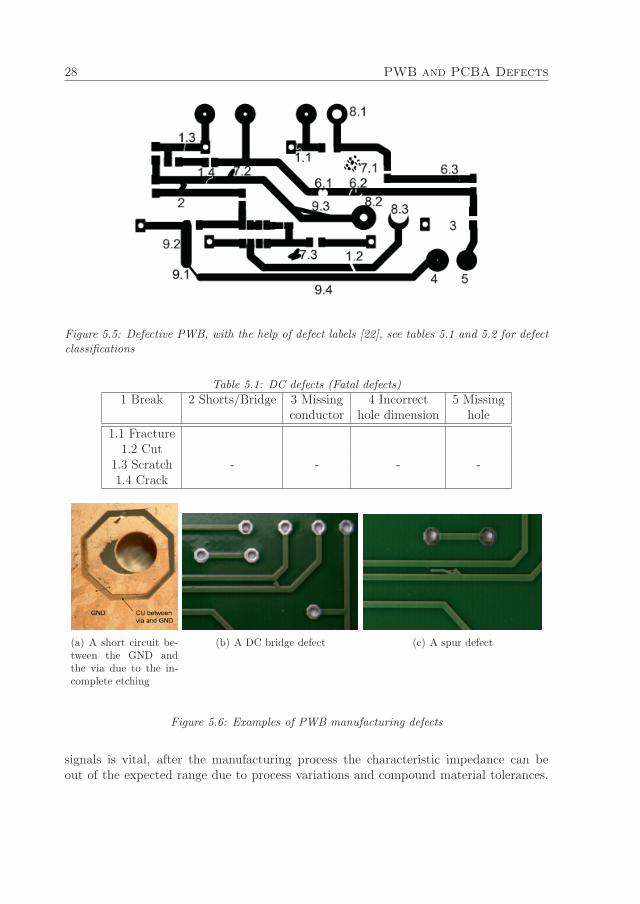
5.3 PWB defects
5.3.1 Etching defects
After the etching process, the assumption that not all the boards are error-free cannotbe ignored in such a way that several types of errors might occur such as trace opens andbridges which are already show stoppers in DC applications, other type of defects suchas mouse bites and spurs and others such as weak traces which can be critical in RF andhigh speed signal applications causing crosstalk and impedance mismatches between theRF devices, of course their severity depend on the frequency of application or the risetime of the clock speed, moreover these type of error can also be problematic in highvoltage application causing bad isolation between the traces. Most of these defects defyregular DC testing and needs advanced test solutions to ensure the quality of the boardbefore going to the assembly process. Figure 5.4 shows a desired PWB after the etchingprocess, unfortunately the probability of achieving that quality is never 1, thus we mightend up with defective boards containing one or several defects as shown in figure 5.5,refer to tables 5.1 and 5.2 for defect classifications [22]. Figure 5.6 shows three types ofPWB manufacturing defects.
Figure 5.4: Error-free PWB.
5.3.2 Characteristic impedance
Characteristic impedance mismatch has a significant impact on signal integrity and powerloss while transferring RF and high speed signals between a source and a destination, Themismatch causes back and forth signal reflections between devices and therefore signalovershoots and undershoots resulting in signal reading errors. Testing the characteristicimpedance correctness for the traces which are designed to carry high speed and RF
28 PWB and PCBA Defects
Figure 5.5: Defective PWB, with the help of defect labels [22], see tables 5.1 and 5.2 for defectclassifications
Table 5.1: DC defects (Fatal defects)
1 Break 2 Shorts/Bridge 3 Missing 4 Incorrect 5 Missingconductor hole dimension hole
1.1 Fracture1.2 Cut
1.3 Scratch - - - -1.4 Crack
(a) A short circuit be-tween the GND andthe via due to the in-complete etching
(b) A DC bridge defect (c) A spur defect
Figure 5.6: Examples of PWB manufacturing defects
signals is vital, after the manufacturing process the characteristic impedance can beout of the expected range due to process variations and compound material tolerances.

5.3. PWB defects 29
Table 5.2: RF defects (Can be critical)
6 Partial open 7 Excessive spurious 8 Pad violation 9 Variationin trace dimensions
6.1 Mouse bite 7.1 Specks 8.1 Under etching 9.1 Smaller width6.2 Nicks 7.2 Spurs 8.2 Over etching 9.2 Larger width
6.3 Pinholes 7.3 Smears 8.3 Breakout 9.3 Excessive trace9.4 Incipient short
Several factors control the characteristic impedance of the trace such as the shape of theedges which can be rounded, rectangular or trapezoidal depending on the etching process,the dimensions of the traces including the width and the thickness, the isolator relativepermittivity and its thickness. Figure 12 shows all these factors. Typically the insulator
Figure 5.7: Factors which control the characteristic impedance of a trace.
which is inserted between the trace and the ground plane is an FR-4 insulator which isconsists of glass fiber weave enforced by the epoxy resin, thus the traces in PWB lies onnon-homogenous dielectric where some traces might be on the top of a substrate where theepoxy resin is dominant and others might be on the top of the substrate where the glassfiber is dominant, see figure 13 this causes variations in the characteristic impedancebetween the traces even in the same PWB [23], Figure 14 illustrates the probabilitydensity of the phase shift measure which represents the characteristic impedance at onefrequency on a trace, according to the figure, the characteristic impedance is not exactlythe same within 20 samples, these variations vary between the three manufacturers M1,M2 and M3. The question is how tolerated this range can be? Paper B discusses this issuethoroughly and provides a quick solution for testing the correctness of the characteristicimpedance using the phase shift method presented in paper A.

30 PWB and PCBA Defects
Figure 5.8: A case where the dielectric is not homogenous. The top trace lies on the dielectricwhere the epoxy is dominant, while the bottom trace lies on the part of the dielectric where theglass fiber is dominant.
2.25 2.3 2.35 2.40
10
20
30
40
50
60
Phase Shift
Pro
babi
lity
Den
sity
M1M3M2
M=2.226StDed=0.006806N=20
M=2.32StDed=0.02271N=20
M=2.338StDed=0.02215N=20
Figure 5.9: Probability density of the phase shift which represents the characteristic impedance.
5.3. PWB defects 31
5.3.3 Process
As addressed in paper B, It is also important to test few samples of PWBs to checkthe process stability by measuring the input impedance of a trace or its characteristicimpedance, this kind of test can be done by the manufacturer before any required processtuning, or can be performed by the client in case of evaluating the quality of the orderedboards for the quality of the process of different vendors before going for high volumeorders. In addition to the process variations impact on the phase shift measure withinthe same batch, figure 14 shows also the difference that can occur between the PWBsuppliers.

32 PWB and PCBA Defects

Chapter 6
Test Strategy
Selecting an effective and efficient test strategy requires the understanding of the prod-uct requirements, production defects and testing budget. Fault coverage, throughput, costand confidence are the factors which can be used to evaluate the test strategy.
6.1 What is a test strategy?
A test strategy describes the road map which determines all the inspection and test activ-ities that have to be applied for delivering a product which conforms to the specifications.The specification may describe both quality and reliability of the product. Creating asuccessful strategy is a key for achieving high faults coverage, high yield and econom-ical testing. Choosing and assembling the test solutions for a successful test strategyrequires understanding the product and the customer expectation, quality and budgetwise [2]. Figure 6.1 shows an example of test strategy, applying different inspections andtest solutions in different phases increases the faults coverage or the testing capabilityof catching all the possible faults which may occur during the manufacturing process,for better understanding the faults coverage refer to figure 6.5 and section 6.3. Differentinspections or different test solutions may overlap in catching some defects however, eachone has the singular ability in detecting one or more type of defects, which justifies itspresence in the test strategy.
6.2 Test solutions
6.2.1 Manual Visual Inspection
As mentioned in the test strategy description, a test strategy may consist of inspectionactivities as well which differ from the traditional test activities that rely on input sig-nals and outputs measurement, the principal of inspection is based on visual comparisonwhere we need a reference with specific tolerances. Inspection reports whether the PCBA
33

34 Test Strategy
Figure 6.1: The test strategy
looks as the reference board or not, however it does not tell whether the board is func-tioning correctly as specified. Inspection offers numerous advantages over testing as it isnoninvasive and does not require any physical contacts. Inspection limits producing de-fective items at an earlier phase of the production and avoids waisting production budgeton defective items, e.g. inspecting boards after the paste application already helps to cor-rect the problems before going further to the solder oven and in the same time applyingimproperly the paste on other items. It is reported that defects which are found throughinspection cost more if they are found by electrical testing, in addition many defects canbe detected by the visual inspection but cannot be detected through a normal continuitytesting such as mouse bites and spurs in the PWB which need special electrical testing,moreover visual inspection is able to find defects which lead to failure only in the field,this is related to the reliability defects, e.g. insufficient solder. Figure 6.2 suggests theinspection first, then test what is not possible to inspect, this way we reduce the cost inthe heavy burden of testing [24]. Manual visual inspection relies on trained inspectorswith the help of light and magnifying glasses, the inspectors are able to recognize a defectduring the PCBA process steps. This method tend to be effective with simple boards,however with the HDI boards, this test solution is not going anywhere with the emergingsmall feature size such as inner layer interconnects, hidden solder joints in BGAs andburied passive components. For a complex PCBA design, although this test solution may

6.2. Test solutions 35
Figure 6.2: Inspection reduces the test burden
be enough for inspecting all the possible defects that can be detected visually, it is costlydue to the time spent in one complex board and it is very possible that it will lead tolow yield [24].
6.2.2 Automatic Optical Inspection (AOI)
This solution came to automate the visual inspection where image processing techniquesand comparison algorithms are involved. If the inspection is referential, a referenceimage is already stored in the processing unit to compare the picture content taken bythe inspector camera. AOI has an exceptional ability in detecting wrong markings andcosmetic flaws and can also detect missing components, shorts, opens, wrong polarity,wrong components, disoriented parts, empty sockets, misaligned and bent parts [24].
6.2.3 Automatic X-Ray Inspection (AXI)
Although AXI solution is expensive, however it is very important to BGAs where allthe solder joints are hidden below the package. In addition to hidden opens and shortsthat AXI can detect, AXI provides benefit in detecting defects which cause reliabilitydegradations such as insufficient melting of the solder balls, excess or shortage in solder[24]. Figure 6.3 shows a defective BGA after the soldering process with quality andreliability issues.
6.2.4 In-Circuit Testing (ICT)
ICT answers this question: Do all components in the DUT work properly? If the answeris yes and the design is correct, the DUT must be correct. ICT is also known as withebox testing, where the test equipment probes are testing for opens and shorts and alsochecking for the correctness of the assembled parts in the PCBA, this solution requiresunderstanding the sub-blocks and the components forming the PCBA as whole, thuspredicting the sub-blocks responses before injecting the inputs signals. ICT solutionsingular ability consists of detecting the inner layer opens and shorts, also it is veryeffective in detecting the defective components which can be fully nonfunctioning or outof tolerance.

36 Test Strategy
Figure 6.3: The x-ray picture shows the inappropriate soldering process resulted in four bridges,one excess solder (shown as a large dot), and insufficient melting of the solder balls (shown assmall dots).
6.2.5 Functional Testing (FT)
Prior to functional testing, we always ask this question: Does the DUT do what is sup-posed to? This solution consists of smaller scope as compared to the ICT, it aims to testonly for the correctness of the end functionality of the product thus it is less effectiveas only limited number of signals are measured which are part of the end functionality.Functional testing has the singular ability in detecting delay faults but it is might not beeffective in detecting some critical faults such as opens which need a proper scenario fortesting. Figure 6.4 shows an example of circuit whose functional testing will not detectthe opens for high frequency noise.
Figure 6.4: Functional testing might not be effective in detecting the opens in high frequencynoise capacitors

6.3. Faults coverage 37
Looking at figure 6.5, the three test solutions scopes are overlapped, one can remarkthat no single solution leads to 100 % faults coverage therefore the necessity of construct-ing a test strategy which satisfies quality, reliability and economy. Figure 6.7 shows atypical test strategy for PCBA containing BGAs, for higher confidence one could addthe functional testing after the ICT if the budget allows, otherwise only for few samples.
Figure 6.5: Overlap between three different test solutions
6.3 Faults coverage
The faults coverage is a figure which describes the ability of a test strategy and a testsolutions in catching the possible defects. This figure is the ratio between the numberof the testable defects with the sum of all possible defects in (%). Figure 6.6 shows anexample of a faults coverage of solder joints testing scenario, where the faults coverageis 4
6� 67 %.

38 Test Strategy
Figure 6.6: A faults coverage scenario
Figure 6.7: A typical production test strategy

Chapter 7
PWB Test Methods
PWB needs to be inspected and tested electrically to ensure quality, for that continuity,isolation and characteristic impedance testings are to be performed separately. Obviously,finding a test method which can perform all these three tests at one go will improve testingin terms of cost and time.
7.1 Inspection
The importance of the inspection is also present while producing a PWB. Althoughinspection offers lower degree of confidence of a proper looking PWB, it has many advan-tages which contribute to cost efficient production and effective testing. Taking a PWBproduction chain where items undergo inspections after the etching and electrical testing,with the inspection we correct the etching problems as earlier as possible and we avoidelectrical testing for defective items. This way we limit producing more defective itemsat the time when the inspection is performed. Several PWB RF defects can be detectedby the visual inspection but cannot be detected through a normal continuity testing suchas mouse bites and spurs in the PWB which need special electrical testing. Figure 6.2is strongly recommended for PWB manufacturing as well. AOI is the technique, whichis used for PWB inspection with either referential or non-referential image comparisonalgorithms. Figures 7.1 and 7.2 describes briefly these algorithms.
7.2 PWB continuity testing
As shown in 7.15(a), continuity testing aims to test against the trace opens and theresistance values which are outside the tolerated range, figure 7.3 highlights some of thecontinuity defects. Typically the measurement is done by injecting a DC current into thetrace and then measuring the voltage across the trace. The resistance value must followρ × l
Awhere l and A are the length and the cross-section area of the trace respectively
and ρ is the electrical resistivity of the conductor. The current intensity is carefully
39

40 PWB Test Methods
Figure 7.1: Basic referential optical inspection algorithm.
Figure 7.2: Basic non-referential optical inspection algorithm.
selected in such way the testing will not be invasive. Although high currents might beuseful to break mouse bites and weak traces, however they might weaken good traces

7.3. PWB isolation testing 41
resulting in short lifetime traces. The ATE which mechanically moves the probes fromtrace to another must be programmed for efficient testing, if the program is done naively,unnecessary tests might be performed which can result in time waste and unnecessaryresource usages, for this purpose the performance is taken in consideration by reducingthe unnecessary tests. Figure 7.4 shows an example of PWB with 4 test points A, B, Cand D, if the test is done naively we will be performing 3 tests for a complete continuitytesting as illustrated in the flowchart 7.5. One might think that we do not need all these3 tests after flagging the unnecessary test points, in this case the unnecessary test pointis A, thus this PWB needs only 2 tests as shown in the flowchart 7.6. Equation 7.1generally determines the number of needed tests for a PWB continuity testing.
CT = NTP −NI (7.1)
Where CT is the number of tests needed for a complete continuity PWB testing, NTP isthe number of the necessary test points in the PWB and NI is the number of the isolatednets (traces) in the PWB.
Figure 7.3: Possible continuity defects [22].
7.3 PWB isolation testing
For better faults coverage, isolation testing is another important step in addition tocontinuity testing. The purpose of isolation testing is to test against DC and RF bridgesbetween the traces such as smears and spurs, see figure 7.15(b). Figure 7.8 highlights

42 PWB Test Methods
Figure 7.4: Example of PWB under test.
some examples of these isolation defects. Similarly to continuity testing, the ATE injectsa DC current between two nets or one net and a group of nets and then measures thevoltage in order to compute the isolation resistance which have to be compared with theminimum threshold value. There exist several isolation test algorithms, let us discuss thefollowing:
1. Net to Net algorithm: In this algorithm, all the possible pairs of traces are testedresulting in NI2−NI
2tests, where NI is the number if the isolated nets in the PWB
and each trace must have at least one accessible test point. Looking at the numberof tests formula, this number can be extremely large when employing flying probessystem, therefore adjacency analysis came to reduce this number by testing onlyadjacent traces which have higher probability of not been fully isolated. Shortly wewill realize that net to net algorithm might not be effective for some applicationswhere isolation is extremely critical. let us assume that the isolation requirementspecifies that the threshold is 70 MΩ, after isolation testing has been performed allthe pairs have passed the test with RAE=120 MΩ, RAD=120 MΩ and RDF=130MΩ. If the traces FE and DC are going to be at the same potential at the endfunctionality of the PCBA, the parallel isolation resistance is RAE//RAD = 60 Ωwhich is no longer bigger than the threshold and therefore the PWB does no longermeet the requirement, this is the net to net algorithm syndrome.
2. True isolation algorithm: True isolation test algorithm came to overcome the weak-ness of net to net algorithm when it comes to the parallel leakage, this time eachnet is tested against the rest of nets, where the positive pole probe is connectedto one net and the negative pole probe is connected to the rest of the nets. Thetest scenario which has been discussed in net to net paragraph will be definitelyfailed. For NI isolated nets in a PWB we need NI tests, the only down side of thisalgorithm is that it does not locate the defect.

7.4. 2-wire measurement method versus 4-wire measurement method 43
Figure 7.5: Naive continuity test algorithm
7.4 2-wire measurement method versus 4-wire mea-
surement method
Since the direct continuity and isolation test methods require probing, it is worthwhilediscussing also two probing techniques. Figure 7.9 illustrates the basic test circuit whichconsists of a DC current generator I, a voltmeter V which indicates the voltage E and twoprobing wires whose total resistance is 2RWire. This circuit is part of an ATE which isemployed to test the resistance of the traces. According to Ohm’s law Rtrace =
EI−2Rwire.

44 PWB Test Methods
Figure 7.6: Improved continuity test algorithm
Can we really use this formula freely? To answer the question, let us look at this scenariowhere the ATE measurement error is ±2 %. Assuming that we are measuring a resistanceRtrace which is intended to be about 0.2 Ω and the probing wires are 1 Ω each. In thiscase the total measurement error will be 0.044 Ω which represents 22 % of the valueof the unit under test, thus the ATE might fail a correct trace. Figure 7.10 illustratesanother circuit which employs 4 wires, only by looking at the circuit, one simply canconclude that the impact of the probing wires is gone and therefore Rtrace =
EI. On the
other hand 4-wire measurement technique increases the maintenance efforts.
7.5 Theoretical background
In the field of microwave when the physical length of the transmission line is much longerthan the wavelength, the transmission is not trivial as it is in the circuit theory. For

7.5. Theoretical background 45
Figure 7.7: A net to net algorithm scenario.
Figure 7.8: Possible isolation defects [22].
a wavelength λ and a physical length L, the voltage and currents can vary in phaseand magnitude over its length and the transmission line becomes an influencing part ofthe magnitude and phase of the received signal. These variations over the line becomesignificant when L > λ
10. Figure 1 shows an transmission line employed to carry a signal
from a source E with an internal impedance ZS to a destination load with an impedanceZL. The transmission line is characterized by its characteristic impedance ZC , its wavevelocity Vp and its length L.
Below are the solutions to the wave equations in a transmission line which relate the

46 PWB Test Methods
Figure 7.9: 2-wire measurement method
Figure 7.10: 4-wire measurement method
back and forward waves.
V (X) = Ae−γX +Be+γX (7.2)
I(X) = Ae−γX
ZC
− Be+γX
ZC
(7.3)
where γ is the propagation constant of the transmission line and A and B can be writtenas follows:

7.5. Theoretical background 47
Vr ZL
ZS
Vi
ZC, Vp, L
xL0
E
Figure 7.11: Reflection in Transmission Line
A =ZC(ZC + ZL)e
+γLE
(ZC − ZS)(ZC − ZL)e−γL − (ZC + ZS)(ZC + ZL)e+γL(7.4)
B =ZC(ZC − ZL)e
−γLE(ZC − ZS)(ZC − ZL)e−γL − (ZC + ZS)(ZC + ZL)e+γL
(7.5)
For the transmission line in figure 1, the voltage reflection coefficient at the load isdefined as the complex ratio of the reflected voltage to the incident voltage which can bewritten as:
ΓL =ZL − ZC
ZL + ZC
= |ΓL|ejθΓ (7.6)
Considering a lossless transmission line, where the propagation constant γ = jβ anda source with an internal impedance ZS, which is equal to the characteristic impedanceof the line ZC .A and B become: A = 1
2E and B = 1
2E |ΓL|ej(θΓ−2βL)
And equation 1 becomes :
V (X) =1
2Ee−jβX +
1
2E|ΓL|ej(θΓ−2βL)e+jβX (7.7)
The voltage along the line is superposed by two parts, the incident voltage which isin the left side and the reflected voltage which is in the right side of equation 6.By keeping the measurement position X and the characteristics of the transmission lineconstant, the phase shift between the incident and the reflected signal will depend onlyon the phase angle of the reflection coefficient at the load which can be written as:θΓ = θ(ZL−ZC) − θ(ZL+ZC), where θ is the phase angle [25]. The trigonometric form of thevoltage at X=0 can be written as :
V (0, t) =1
2E cos(ωt) +
1
2E|ΓL| cos(ωt+ θΓ − 2βL) (7.8)
The single probe tester uses the notion of voltage reflection which is described aboveas a main vehicle to detect differences between a correct PCW trace and a defective one.

48 PWB Test Methods
The source of the difference will be presented in the phaser of the reflection coefficientwhich depends on the load. Figure 1.5 illustrates a complete schematic of the singleprobe tester implementation.
7.6 Characteristic impedance testing
In 5.3.2, we discussed the motivations behind the characteristic impedance testing, thissection gives insight into how to test the characteristic impedance ZDUT of a transmit-ting medium . The measurement is based on a method called time domain reflectometry(TDR) which uses the fundamental behavior of signal reflections between a source anddestination through a transmitting cable. Figure 7.12 shows a basic signal transmis-sion circuit from a source to destination, the source Vs is characterized by its internalimpedance Zs, the transmitting medium is characterized by its characteristic impedanceZc and the transmission delay Td , which will be used for transmitting a signal to aload ZL. Figure 7.13 is a lattice diagram which illustrates how back and forth reflec-tions are shaping the signal at the source point A and at the destination point L beforereaching its steady state, where ΓL = ZL−Zc
ZL+Zcis the reflection coefficient at the load and
Γs =Zs−Zc
Zs+Zcis the reflection coefficient at the source. Using data provided by the lattice
diagram, DTR can measure the characteristic impedance by adding an extra sampler atthe source. As shown in figure 7.14(a) By sampling the voltage at the source after 2×Td,the characteristic impedance of ZDUT can be deduced as ZDUT = Zc
VA
Vs−VA.
Figure 7.12: Transmitting a step signal from source to destination load
7.6.1 How does single probe test method affect PWB testing?
Single probe test method which is published in paper A, is based on phase shift measure-ment between the incident and the reflected signals, the incident signal is injected intothe trace under test, the measured signal carries the information about the correctness ofthe trace when compared with a reference value of the same trace in a correct board, thislatter has already passed continuity and isolation testing and used for collecting phase

7.6. Characteristic impedance testing 49
Figure 7.13: Lattice diagram
(a) DTR circuit (b) A microstripline as a DUT
Figure 7.14: DTR circuit for the characteristic impedance measurement
shift references. For a given design with NI isolated traces and NA adjacent pairs, leadsto the reduction of the number of tests from (NI+NA) tests to NI tests as isolation andcontinuity are performed in one go as shown in figure 7.15. Characteristic impedanceverification is part of the quality process of high speed PWBs. The single probing methodallows a quick referential verification of the characteristic impedance and avoiding DTRtools and setup. This also implies the use of this method in evaluating the stability ofPWB manufacturing process by the manufacturer for better yield or by the customer forselecting a better vender, paper B discusses this issue thoroughly.

50 PWB Test Methods
(a) Continuity test (b) Isolation test
(c) Isolation and continuity in onego, using our RF method
Figure 7.15: Effect of our contribution on PWB testing

Chapter 8
Test Technology
Volume and time-to-market are two main factors which are involved when selectingbetween different test technologies. Bed-of-nails is expensive but its test time is expressedin seconds while flying probes system is flexible but its test time is expressed in severalminutes.
8.1 Bed-of-nails
Bed-of-nails is a test equipment which is designed for a specific design to be tested afterthe production. Bed-of-nails allows to execute what ever test vectors the test engineerhas proposed for PCBA ICT or for PWB continuity and isolation testing. Bed-of-nailsis characterized by high throughput as nodes contacts are made as soon as the test unitis closed, thus the test time is up to the electrical switchings in the test unit and thenumber of test points in the board, it can be concluded when referring to figure 8.1.Bed-of-nails is an expensive test equipment to setup, thus it is only suitable for highvolume production. To justify bed-of-nails purchase and investment, its expenses mustbe negligible as compared to the profit [26].
8.2 Flying probes system
Flying probes system is a test equipment which is flexible for probing and very effectivefor fine-pitch boards with a limit of between 100 and 150 μm [27]. The equipment movesits probe form one test node to another, where the mechanical movements are involvedand the test time is dominated by the mechanical performance of the arms holding theprobes. The need of the mechanical reposition of the probes between the tests results inlow throughput which represents the fundamental drawback of such systems, typically itis 5 to 10 Test Points per second (TP/s), for complex HDI applications. Flying probessystem is appropriate only for low volume production [26]. Our test technique in paperA and C allows to perform two tests instead of one when having a two-probe system.
51

52 Test Technology
Figure 8.1: Bed-of-nails.
Several issues as presented in subsections 8.2.1 and 8.2.2 need to be taken into accountwhen considering flying probes system as a test equipment.
8.2.1 Test points
For effective and non destructive testing some test points have higher priority over othersto be selected. it recommended to probe on specifically designed test pads, SMD padsand vias and on rigid through-hole component leads. On the other hand one shouldreduce probing on IC pins and SMD devices where the pin size is close to the land size[28].
8.2.2 Optimize test times
In addition to the parallelism of several probes and the test technique used to performtesting, the mechanical movements which dominate the test time can be optimized byreducing the movement of the probes. Bridges testing can be optimized to high percentagebridges by the use of a proximity variable. Only pads within the range of the proximityvariable are tested against each other for bridges. Moreover placing high component inthe test side or area should be avoided in order to avoid probes moving higher to thez direction. The fundamental idea here is to keep short travel distance of the movingprobes [28].
8.2.3 Single probe tester and the current probing technology
Our contribution reduces 50 % of the probes when applied to bed-of-nails for PWBstesting, which translates to significant cost improvement, see figure 7.15. Applying thistechnique to flying probes system with two probes, only one probe will be needed asPWB ground plane is used as probe reference. For a given design with NI isolated tracesand NA adjacent pairs, only NI tests will be needed, this is a drastic improvement on

8.3. Automatic X-Ray Inspection (AXI) 53
the test time as the mechanical performance of the probes dominates the test time. Ofcourse one could trade more probes for even better performance.
8.3 Automatic X-Ray Inspection (AXI)
As discussed in the history chapter 2, BGA packages with hidden solder joints are prone toDC soldering defects and reliability issues although the joints passed the Boundary Scantesting. Excess, insufficient solder paste, insufficient melting and solder void will degradethe performance and cause the PCBA failure at some time during its field operation [29].Automatic X-Ray Inspection (AXI) came specifically to overcome this issues. After thesoldering process, BGA packages need to undergo AXI for reliability related defects asit reveals many defects in solder joints that may not be detected with AOI and otherelectrical test technologies. The following are the advantages of AXI over the other testtechnologies:
• Insufficient solder paste and insufficient melting
• Solder void
• Excess in solder
• Some other parameters of specific solder joints such as dimensions, which help totune the process for better yield.
Figure 6.3 shows an X-Ray image with some of the mentioned defects, while figure 8.2shows the void defect where AXI outperforms the other test technologies. The only cases
Figure 8.2: Void defect in solder ball. (Source: IMAPS, DfR solutions)
where AXI is not able to detect the defect are wrong component value and defectivecomponent cases.

54 Test Technology
8.4 Automatic Optical Inspection (AOI)
Due to the increase of the PCBA complexity and short time to market, manual visualinspection is no longer viable in terms of quality and throughput. AOI test technologycame to automate the visual inspection where image processing techniques and compar-ison algorithms are involved. If the inspection is referential, a reference image is alreadystored in the processing unit to compare the picture content taken by the inspector cam-era. The only AOI exceptional abilities in detecting defects are when wrong markingsand some cosmetic flaws are involved, on the other hand AOI technology can also detectmissing components, shorts, opens, wrong polarity, wrong components, disoriented parts,empty sockets, misaligned and bent components which can be detected by the other testtechnologies. AOI has an important role in applying a cost effective test strategy bydetecting defects early in the production line. Typically, AOI is applied just after thesoldering process before any signal measurement, this way quick actions are taken beforeproducing high number of defective boards. If required, It can also be applied before thereflow to check for the pick and place operation.

Chapter 9
Summary of Appended Papers
The following contributions include paper A, paper B, paper C and paper D whichtarget fundamentally the improvement of electronics production testing.
9.1 Paper A: Single Probe for Bare Board Continu-
ity and Isolation Testing (IMAPS, 2011. Out-
standing Paper Award)
This paper discusses a solution for improving the PWB test throughput and thus improv-ing a complete test strategy, by investigating the single probe testing using RF signalinjection and measuring the phase shift between the incident and the reflected signals.Defects in the interconnect such as opens and bridges are visible in the phase shift valuewhen comparing it to the reference one which corresponds to an error-free interconnect.In this paper, we shown the feasibility of the single probe tester for real application bytaking a case study of defective produced bare board whose designs are originated formthe same design of a correct bare board. In the defective designs we introduced severaldefects such as open, bridge, RF bridge, smaller width trace. According to the conductedexperiments, the idea is very promising to be taken in use in a real ATE (Automatic TestEquipment) for bare board and loaded board with open sockets. At the highest sensitiv-ity of the phase shift detector, the prototyped tester is capable to distinguish between adefective and error free board with significant margins in case of defects such as opens,DC and RF bridges, exceeded and different width lines. The margin in the measurementbetween a defective and a correct board, which depends on the type of the defect is about7 % to 68 %. Result figures have been compared to the simulation figures and we alsoproposes a complete process which describes the effective use of the method. The advan-tages of this method consist of improving the throughput when testing PWBs by gainingthe probe which is supposed to close the loop for the ground when using the DC currenttesting and employ the probe for another trace, thus parallel testing. This method alsoallow us to reduce the cost in the mechanics once we reduce one probe instead of two if
55

56 Summary of Appended Papers
the mechanical design and implementation are considered an issue.
9.2 Paper B: Impact of PCB Manufacturing Process
Variations on Trace Impedance (IMAPS, 2011.
Best paper of the session award)
This paper provides insight into the impact of PCB manufacturing process on traceimpedance. Using the statistical methods, the paper demonstrates that the characteris-tics of PCBs may vary across different suppliers and across different production batcheswithin the same PCB manufacturer. These variations may not be tolerated in applica-tions where reflections are restricted to be within a specific range. As a measurementvehicle, we exploited the single probe tester, which is discussed in paper A, due to itsbenefit in quick checking whether or not a difference is occurring between two PWBs.Three PCB populations have been chosen and each population represents one supplier.The conclusions were drawn after running the T-tests to assess the significance of theobtained difference occurring between the PCBs. Based on the computed P-values, allthe three batches are different from each other in the mean of the measured phase shiftwith 95 % confidence. The difference between the measured and the expected charac-teristic impedance is found as 3 %, 10 % and 20 % for these three manufacturers. Wealso witnessed board-to-board variations even within the same batch and from the samesupplier due to the process instability by looking at the probability density of having thesame phase shift that is equal to the mean. Some samples shown 2.6 % to 3.5 % differenceabove the mean. These figures rise an alarming flag for the electronics manufacturerswho deal with high volumes for assessing the quality of the PCBs when switching to anew supplier and before moving to high volume assembly phase. Suppliers as well cantake the advantage of this paper to assess their process stability by sampling the qualityusing the phase shift method measurement for fast inspection instead of dealing withmore work one using the network analyzer.
9.3 Paper C: Reflection phase shift for PWB and
PCBA Production Testing (Journal of Micro-
electronics and Electronic Packaging)
This paper is an extension of paper A, where we investigated the feasibility of applyingthe single probe tester to loaded board testing. The good news is that the approachis always capable in detecting the open defects with high margins when probing on thetop of IC pins as the pin impedance is much different as compared to the interconnectimpedance. Our test cases shown 40 % and 33 % as margins between the measurementsof correct and defective soldered pins, this makes it a strong candidate approach to beapplied officially to PCBA testing where physical probing is feasible. The technique can

9.4. Paper D: Impact of etch factor on characteristic impedance,crosstalk and board density (IMAPS, 2012) 57
be applied to the complete layout or to boost the test strategy where the applied testsolutions are not covering 100 % of the possible defects.
9.4 Paper D: Impact of etch factor on characteristic
impedance, crosstalk and board density (IMAPS,
2012)
This paper extends the discussion about the impact of the manufacturing process onPWBs, this time we look more specifically at the etching, which is influenced by the man-ufacturing process and it is one of the factors which control the characteristic impedance.Etching types can fall in three different categories which are flat, trapezoidal with vari-ations in the angle or rounded with variations in the depth. In this paper we planed topresent the effect of three different etching shapes on the characteristic impedance andthe crosstalk of two edge-coupled microstrip lines. On the other hand, it is concludedthat one could trade the characteristic impedance error for space and raw material whena 90◦ etch angle process is feasible, it could be beneficial for high production volumesand can be a cost saving source if it results in reduced number of layers in HDI boards.Employing similar idea and trading characteristic impedance error for crosstalk reduc-tions lead to a small improvement which can be beneficial in applications where crosstalkreduction has a high priority.

58 Summary of Appended Papers

Chapter 10
Other Publications
Apart from the test contributions, additional papers are published in the field of lowpower Field-Programmable Gate Array (FPGA) implementations design.
10.1 Book Chapter: Data-Stream-Driven Comput-
ers are Power and Energy Efficient (IGI Global,
2012)
Abdelghani Renbi
It is believed that data-stream-driven computing is power and energy efficient ascompared to its counterpart, instruction-stream-driven computing. This latter requiresmemory access and memory control overheads while the processor is fetching task in-structions from the memory. The programmer describes all the tasks as instructions inthe program memory. On the other hand data-stream-driven computer is already config-ured or hardwired for a specific computing operation, no memory is required apart fromdata storage. In some contexts we refer to data-stream-driven computers as acceleratorsor single-purpose processors. This chapter discusses the benefit of data-stream-drivencomputing for better power and energy efficiency. We took matrix multiplication as anexample application to compare the power and energy dissipations between load/storeand non-instruction fetch-based architectures. We witnessed that single-purpose pro-cessor reduces almost 100 % of the dynamic power when replacing the general-purposeprocessor. With the current mainstream transistor technology, morphware platformsthat allow massive parallelism are the potential key for data-stream-driven computerimplementations to saving energy in battery-powered embedded systems and to solvethe dissipated power dilemma, as the heat becomes the bottleneck of traditional highfrequency processors. If the same strategy is applied to mainstream computers and datacenter servers, we will not only reduce electricity bills but we will also contribute togreener computing by lowering the IT sector’s CO2 emissions.
59

60 Other Publications
10.2 Paper E: Non-Instruction Fetch-Based Archi-
tecture Reduces Almost 100 Percent of the Dy-
namic Power and Energy (IEEE/ACM, 2010).
Abdelghani Renbi, Lennart Lindh and Jerker Delsing
This paper demonstrates the benefit of FPGAs for better power and energy efficiencywhen exploited for non-instruction fetch-based architecture. By replacing load/storearchitecture by non-instruction fetch-based designs for matrix multiplication, we reducedalmost 100% of the dynamic power. Hence reconfigurable computing is the potential keyto saving energy in battery-powered embedded systems and to solve the dissipated powerdilemma, as the heat becomes the bottleneck of traditional high frequency processors.If the same strategy is applied to mainstream computers and data center servers, wewill not only reduce electricity bills but we will also contribute to greener computingby improving the IT sector’s CO2 emissions. The work involves three different designs,which multiply two matrices A and B of nxn 32-bit items and store the result in Cmatrix of nxn 64-bit items. The first two designs employ a single-purpose processor withdifferent number of storage registers 2n and 2n2 and the third design uses a computersystem piloted by NIOS II/e processor with on-chip memory. The designs were capturedin VHDL language and prototyped on an Altera Cyclone II EP2C35F672C6 device. Bothsynthesis and place&route steps were performed with Quartus II 6.0 Web Edition. Theexperiments were made on Altera DE2 board. In this paper we have also clarified furtherthe power estimation error of Altera power estimation tools, which we have evaluated in[30].
10.3 Paper F: Power and Energy Efficiency Evalu-
ation for HW and SW Implementation of nxn
Matrix Multiplication on Altera FPGAs (ACM,
2009)
Abdelghani Renbi and Lennart Lindh
Matrix multiplication is most often involved in graphics, image processing, digital signalprocessing, robotics and control engineering applications. In this paper we compared andanalyzed the power and energy consumption in three different designs, which multiplytwo matrices A and B of nxn 32-bit items and store the result in C matrix of nxn 64-bititems. The first two designs use FPGA HW with different number of storage registers2n and 2n2 and the third design uses a computer system piloted by NIOS II/e processorwith On-Chip memory. We showed that NIOS II/e is not an energy efficient alternativeto multiply nxn matrices compared to HW matrix multiplier on FPGA. Since our targetFPGA is the Altera cyclone II family, we also had to find one acceptable method tomeasure the real power consumption in the FPGA device.

Chapter 11
Conclusion
This thesis presented an introduction to electronics testing, with test motivations andchallenges that PCBA and PWB test business is facing. Testing PCBA and PWB is partof the electronics production which has a great impact on the profitability. Always highthroughput and low cost testing is needed but for high quality and reliability.
The important part in this thesis as contribution is presented in paper A and C, whichanswers some of the research questions. Based on the achieved results, single probe testeris feasible based on phase shift measurement to test PWBs and PCBAs. The feasibilityof this technique leads to several implications on the current probing technologies, suchas improving significantly the test cost in reducing the test resources which translatein probes and their related mechanical design, manufacturing and maintenance. Otherimplication is that by keeping the same resources of the current test technologies, thetest throughput is improved using the presented solution.
This single probing technique indicates other great benefits on SBU technology totest bare HDIs, through-hole, blind and buried vias can be tested only from one side,moreover interconnects which are connecting embedded components with the upper layerin HDIs can be tested through one single test point.
In addition to all these advantages, the single probe tester is believed to provide quickcharacteristic impedance correctness testing and fast PWB manufacturing process eval-uation as discussed in paper B, otherwise we have to deal with TDR setup and samplingtools or other network analyzer methods which are not practical for mass testing. Onthe other hand this technique is only comparative, which means that always a referencedata of an error-free board which has already underwent through direct electrical testing,must be available for comparison.
61

62 Conclusion

References
[1] S. F. Scheiber, Building A Successful Board-Test Strategy, 2nd ed. Newnes, 2001,ch. What Is a Test Strategy?, pp. 1–4.
[2] ——, Building A Successful Board-Test Strategy, 2nd ed. Newnes, 2001, ch. WhatIs a Test Strategy.
[3] B. Davis, “Economic modeling of board test strategies,” Journal of Electronic Test-ing, p. 2, 1994.
[4] S. F. Scheiber, Building A Successful Board-Test Strategy, 2nd ed. Newnes, 2001,ch. Test-Strategy Decisions, p. 290.
[5] ——, Building A Successful Board-Test Strategy, 2nd ed. Newnes, 2001, ch. Test-Program Development and Simulation, pp. 237–240.
[6] D. Staff. (2008) Design for testability - origin and evolution. [Online]. Available:http://articles.dsiintl.com
[7] S. F. Scheiber, Building A Successful Board-Test Strategy, 2nd ed. Newnes, 2001,ch. Test Methods, pp. 55–58.
[8] K. P. Parker, The Boundary-Scan Handbook, 3rd ed. Kluwer Academic Publishers,2003, ch. Boundary-Scan Basics and Vocabulary, pp. 2–7.
[9] N.Kimmance, “Bare-board testing,” Circuit World, vol. 9, no. 42-43, 1983.
[10] C. F. Coombs, Printed Circuits Handbook, 5th ed. McGraw-Hill Professional Pub-lishing, 2007, ch. HDI Bare Board Special Testing Methods.
[11] M. L. Bushnell and V. D. Agrawal, Essentials of Electronic Testing for Digital,Memory, and Mixed-Signal VLSI Circuits. Springer, 2000, ch. Introduction, pp.6–8.
[12] IPC, “Ipc-tm-650 standards.” [Online]. Available: http://www.ipc.org/ContentPage.aspx?pageid=ELECTRICAL-TEST-METHODS
[13] C. F. Coombs, Printed Circuits Handbook, 5th ed. McGraw-Hill Professional Pub-lishing, 2007, ch. Properties of Base Materials.
63

64 References
[14] ——, Printed Circuits Handbook, 5th ed. McGraw-Hill Professional Publishing,2007, ch. Component-to-PWB Reliability.
[15] W. Engelmaier, “Solder creep-fatigue model parameters for sac and snag lead-freesolder joint reliability estimation.” [Online]. Available: http://www.ipcoutlook.org/pdf/solder creep fatigue ipc.pdf
[16] S. Oresjo, “A new test strategy for complex printed circuit board assemblies,” Agi-lent Technologies, Inc., http://www.home.agilent.com, Tech. Rep., 1999.
[17] P. Girard, N. Nicolici, and X. Wen, Power-Aware Testing and Test Strategies forLow Power Devices. Springer, 2009, ch. Power Issues During Test.
[18] M. L. Bushnell and V. D. Agrawal, Essentials of Electronic Testing for Digital,Memory, and Mixed-Signal VLSI Circuits. Springer, 2000, ch. Introduction, pp.12–13.
[19] A. Verma, “Designing test strategies for modern pcb assembly,” Teradyne,http://www.teradyne.com/atd/resource/recording/testStrategy/testStrategies.pdf,Tech. Rep. 11.
[20] S. F. Scheiber, Building A Successful Board-Test Strategy, 2nd ed. Newnes, 2001,ch. What Is a Test Strategy, pp. 21–23.
[21] K. Rajewski. (1999) Defect minimization methods for a no-clean smt process.
[22] F. R. Leta, F. F. Feliciano, and F. P. R. Martins, “Computer vision system forprinted circuit board inspection,” ABCM Symposium Series in Mechatronics, vol. 3,pp. 623–632, 2008.
[23] S. H. Hall, Advanced Signal Integrity for High-Speed Digital Designs, 1st ed. Wiley-IEEE Press, 2009, ch. Electrical Properties of Dielectrics, pp. 274–279.
[24] S. F. Scheiber, Building A Successful Board-Test Strategy, 2nd ed. Newnes, 2001,ch. Inspection as Test.
[25] H. J. Visser, “Array and phased array antenna basics,” in Array and Phased ArrayAntenna Basics. Wiley, 2005.
[26] C. F. Coombs, Printed Circuits Handbook, 5th ed. McGraw-Hill Professional Pub-lishing, 2007, ch. Bare Board Test Equipment.
[27] H. Holden, The HDI Handbook, 1st ed. BR Publishing, Inc, 2009, ch. ElectricalTest of High-Density Interconnects, pp. 419–427.
[28] T. C. Corp, “Flying probe guidelines,” Test Coach Corporation,http://www.testcoachcorp.com/finnProducts/downloads/DFT/DFT.pdf, Tech.Rep.

References 65
[29] S. H. Peng, “Bga void detection in x-ray images based on a new blob detector,”Dankook University, Yongin, South Korea. IEEE, 2011.
[30] R. Abdelghani and L. Lennart, “Power and energy efficiency evaluation for hw andsw implementation of nxn matrix multiplication on altera fpgas,” in FPGAworld’09: Proceedings of the 6th FPGAworld Conference. New York, NY, USA: ACM,2009, pp. 45–51.

66 References

Part II
67

68

Paper A
Single Probe for Bare BoardContinuity and Isolation Testing
(Outstanding Paper Award)
Authors:Abdelghani Renbi and Jerker Delsing
Reformatted version of paper originally published in:IMAPS 2011 - Long Beach, California, USA, 44th International Symposium on Micro-electronics.
© 2011, IMAPS, Reprinted with permission.
69

70

Single Probe for Bare Board Continuity and
Isolation Testing
Abdelghani Renbi and Jerker Delsing
Abstract
Bare board testing is vital before components loading. Defects after the PCB manufac-turing process are possible such as opens, bridges, near-opens, near-bridges and charac-teristic impedance mismatches due to process variations and compounding raw materialtolerances. Moreover, defects might cost about ten times more when detected in the nexttest phase, another motivation for unpopulated board test is loading expensive compo-nents on a set of defective boards might be economically catastrophic. Flying probesystems, which were developed in late 1980’s are commonly used and favorable to per-form bare board isolation and continuity testing, especially when the volume is not bigenough to justify bed of nails purchase. Flying probe system performance for a given bareboard depends on the test algorithm, the mechanical speed and the number of probes.To reduce the cost on expensive test probes and probe maintenance and to accelerate thetest time, this paper presents a new and cost efficient approach to test unpopulated andpopulated board with open sockets, using a single probe. Specifically, a coaxial probeinjects one frequency signal into the PCB trace, the phase shift between the reflectedsignal from the trace and the incident wave is detected and compared with the nomi-nal value, which has been captured from a defect free board, which already underwentdirect continuity and isolation testing. The conducted experiments have shown a goodfeasibility for practical use in the ATE (Automatic Test Equipment) for bare board andloaded board with open sockets. At the highest sensitivity of the phase shift detector,the prototyped tester is capable to distinguish between a defective and error free boardwith significant margins in case of defects such as opens, DC and RF bridges, exceededand different width lines. The margin in the measurement between a defective and acorrect board, which depends on the type of the defect is about 7 % to 68 %.
1 Introduction
Flying-probe systems have joined the mainstream in late 1980’s and become popularfor their ability of performing ICT without the need of expensive bed of nails and theirability of fine pitch access [1]. The main factor, which drove the electronics manufacturersto use flying probe systems is cost-effective testing especial when the volume does notjustify bed-of nails purchase, however flying-probe systems are prone to slow performancedue to the mechanical movements of the probes. The success of flying probe-systems isrelated to their success in entering in high volume productions, however this still open
71

72 Paper A
issue to the electronics manufacturers. In the past costumers have not been pressuringbare boards suppliers for electrically tested products, due to the evolution of small sizeelectronics, this tradition has already started changing, today’s costumer is more likelyto buy tested products. It has been reported that failed bare board represent 5 % insingle sided boards, 5 % to 10 % in plated-through hole boards and any value between10 % and 100 % in multi-layers boars [2].
2 Related work
Apart from the direct test methods for bare boards, the author of [3] has mentioned thatthere exist few bare board test methods which are unique to the direct electrical tests.Capacitive and electromagnetic coupling is the main principal. He stated that thesemethods are reliable when detecting DC shorts and opens, but may be less effective indetecting distributed high resistance connections. Capacitive measurement which wasstated is based on measuring the ratio of the variation of time and the voltage levelwhen a constant current is flowing into a capacitance trace. More over nothing has beenpublished explicitly within the bare board test methods. It seems that there is a greatneed of an academic contribution in this area.
3 Theoretical Background
In this section we will discuss three topics in microwave theory, which build the groundof understanding the workhorse of our prototyped idea for the single probe tester.
3.1 Wave Reflection
In the field of microwave when the physical length of the transmission line is much longerthan the wavelength, the transmission is not trivial as it is in the circuit theory. Fora wavelength λ and a physical length L, the voltage and currents can vary in phaseand magnitude over its length and the transmission line becomes an influencing part ofthe magnitude and phase of the received signal. These variations over the line becomesignificant when L > 10λ. Figure below shows an transmission line employed to carrya signal from a source E with an internal impedance ZS to a destination load with animpedance ZL. The transmission line is characterized by its characteristic impedanceZC , its wave velocity Vp and its length L.
Below are the solutions to the wave equations in a transmission line which relate theback and forward waves.
V (X) = Ae−γX +Be+γX (1)
I(X) = Ae−γX
ZC
− Be+γX
ZC
(2)

3. Theoretical Background 73
Vr ZL
ZS
Vi
ZC, Vp, L
xL0
E
Figure 1: Reflection in Transmission Line
where γ is the propagation constant of the transmission line and A and B can be writtenas follows:
A =ZC(ZC + ZL)e
+γLE
(ZC − ZS)(ZC − ZL)e−γL − (ZC + ZS)(ZC + ZL)e+γL(3)
B =ZC(ZC − ZL)e
−γLE(ZC − ZS)(ZC − ZL)e−γL − (ZC + ZS)(ZC + ZL)e+γL
(4)
For the transmission line in figure 1, the voltage reflection coefficient at the load isdefined as the complex ratio of the reflected voltage to the incident voltage which can bewritten as:
ΓL =ZL − ZC
ZL + ZC
= |ΓL|ejθΓ (5)
Considering a lossless transmission line, where the propagation constant γ = jβ anda source with an internal impedance ZS, which is equal to the characteristic impedanceof the line ZC .A and B become: A = 1
2E and B = 1
2E |ΓL|ej(θΓ−2βL)
And equation 1 becomes :
V (X) =1
2Ee−jβX +
1
2E|ΓL|ej(θΓ−2βL)e+jβX (6)
The voltage along the line is superposed by two parts, the incident voltage which isin the left side and the reflected voltage which is in the right side of equation 6.By keeping the measurement position X and the characteristics of the transmission lineconstant, the phase shift between the incident and the reflected signal will depend onlyon the phase angle of the reflection coefficient at the load which can be writhen as:θΓ = θ(ZL−ZC) − θ(ZL+ZC), where θ is the phase angle [4]. The trigonometric form of thevoltage at X=0 can be written as :

74 Paper A
V (0, t) =1
2E cos(ωt) +
1
2E|ΓL| cos(ωt+ θΓ − 2βL) (7)
3.2 Frequency Mixing
Frequency mixers are mostly used in applications when phase shift information is re-quired. The principal upon which phase shift detection rests is that mixing two signalswith an equal frequency results in a DC voltage after a proper filtering of higher fre-quency components as shown in figure 2. Mathematically, a frequency mixer output canbe described as:
Vf = A cos(ω1t+ φ1)B cos(ω2t+ φ2) (8)
which reminds us of an AM modulator output. If the input signals have the same fre-quency 2πω we simply modify the function from an AM modulation to a phase detection.
Vf =AB
2[cos(φ1 − φ2) + cos(2ωt+ φ1 + φ2)] (9)
By filtering out the higher frequency component, Vf will be only a function of the phaseshift between the two input signals.
Vf =AB
2cos(φ1 − φ2) =
AB
2cos(Δφ) (10)
Where Vf is the output voltage of the mixer, A cos(ω1t + φ1) is the signal at the inputLO and A cos(ω1t+φ1) is the signal at the input RF . Figure 2 shows that the maximum
LO
RFπ
Low passfilter
Vf
Vf ΔΦ
δΦ
Figure 2: Principal of phase shift detection
and the minimum of the function appear at Δφ = 0 and Δφ = π respectively, based on

4. Methodology 75
the implementation the term AB2cos(Δφ) might inherit a negative sign and therefore the
maximum and minimum will exchange the positions. According to the plotted fuctionin figure 2 we can also remark that the highest sensitivity of the phase shift detectorcan be achieved at the linear region of the plot which is around Δφ = π
2, let us say
the linear region is determined by the segment whose X coordinates are π2± δφ. This
segment appears at each nπ2± δφ, where n is an odd integer. The sensitivity
Δ Vf
Δφcan be
improved by increasing the maximum of the output function, the higher maximum thebetter sensitivity will be [5].
3.3 Reflection Detection
Directional couplers are commonly deployed for coupling a proportion of a traveling wavein a transmission line out through another port. The concept behind is that by settingtwo transmission lines close enough to each others an amount of power will be travelingin the neighborhood line. Figure 3 shows a 4-port directional- coupler, which can be used
3
1
4
2Directional coupler
Figure 3: Directional coupler
to sense the reflected signal at the port 4. It consists of 4 ports: Port (1), which refersto the main device input, Port (2) , which refers to the main device signal output, port(3) which is coupled with Port (1) for the incident signal and finally the isolated Port(4), which is coupled to the port (2) for sensing the reflected signal. Figure 4 in section4, shows how the directional coupler is involved in our tester schematics, it can be seeneasily that the above description of the directional coupler matches with the purpose.
4 Methodology
The single probe tester uses the notion of voltage reflection which is described in insection 3.3 as a main vehicle to detect differences between a correct PCB trace and adefective one. The source of the difference will be presented in the phaser of the reflec-tion coefficient which depends on the load. There are three main parts in the tester,the directional coupler which senses the reflected signal and the frequency mixer which

76 Paper A
Transmission Line
PCB Traceas ZL
Amp
AmpAmp
Directional Coupler
FrequencyMixer
SignalConditioning ADC Comparaison
UnitFail/PassDisplay
VCO
50Ω
Figure 4: Schematic of the Single Probe Tester
detects the phase shift between the incident and the reflected waves. As the test natureis referential, the comparison unit stores the phase shift references of each trace of anerror free board for comparison with the unit under test and therefore falling or passingthe test. Considering a short microstrip line as a unit under test, the input impedanceZL can be written as follows using one π cell which is illustrated in figure 5.
ZLCTrace/2
LTrace
CTrace/2
Figure 5: A π cell of a lossless microstrip line
ZL =j(1− lcω2)
lc2ω3 − 2cω(11)
If the characteristic impedance of the transmission line is 50 Ω, we can write:
θΓ = 2arctan[1− lcω2
100cω − 50lc2ω3] (12)

5. Experiment and Simulation 77
where c = CTrace
2and l = LTrace. Theoretically any change in a trace shape or dielectric
thickness and characteristics will be seen in the phase shift described by the above equa-tion.In this work we refer to one bare board design which consists of few 50 Ω traces withW=1 mm, h=0.5 mm, t=18 um and FR4 substrate, where W is the width of the trace,h is the hight of the inserted substrate between the trace and the ground plane and t isthe thickness of the cooper foil. To model the possible alarming production defects, weintroduced an open, an RF bridge, a DC bridge and a weaker trace in our design andeach defective board contains one defect only, see figure 6.
Open DC bridgeRF bridge
Smaller width
Figure 6: Reference bare board with some defect locations.
5 Experiment and Simulation
5.1 Simulation
Knowing that the board traces will be tested only at the frequencies which lead to thehighest sensitivity of the phase shift detector, in other words, the frequencies which leadto ±nπ
2. We performed S11 simulations on each correct and defective trace separately.
The effect of 0.45 m length and 2.1 × 10⁸ m/s propagation speed of the probe on thetotal phase shift has been added manually after measuring the propagation speed of thetransmission line of the probe. Equation 7 describes the total phase angle of the reflectedsignal. The phase angle of S11 is totaly linear with a negative slope. From the linearfunction relating the frequency and the phase angle of S11 of the correct trace we extractedthe frequencies which lead to the odd multiples of the part which is due to the probe

78 Paper A
length and speed. On the other hand we extracted the phase angle of those frequenciesin the function relating the frequency and the phase angle of S11 of the defective trace,then the difference in the phase shift can be evaluated. It is clearly seen that the biggern is the more visible the defect is. The following tables summarize the collected data ofthe phase shift information for the different introduced defects, ΦC and ΦD refer to thephase shift which corresponds to the correct and the defective trace respectively. Figure8 shows that the RF bridge defect is characterized by the smallest margin followed by theopen defect as the test point is far from the location of the break, on the other hand ifthe test is performed at the side which is closer to the break, the margin will be greater.Of course we do not want to double test the trace as the original goal is to improve thetest time and the test maintenance cost, increasing the factor n and improving the phaseshift sensitivity is the key solution for this kind of limitations. Nevertheless we will seethat this margin is visible enough at the voltage level as the test was ran at the highestsensitivity of the phase shift detector.
Table 1: Phase shift data for different defects when n=3.Defect Test ΦC ΦD Δ
frequency
Open 151 MHz -270◦ -265◦ 5◦
DC Bridge 145 MHz -270◦ -309◦ -39◦
RF Bridge 143 MHz -270◦ -271◦ -1◦
Smaller 155 MHz -270◦ -247◦ 23◦
Width
Table 2: Phase shift data for different defects when n=5.Defect Test ΦC ΦD Δ
frequency
Open 251 MHz -450◦ -440◦ 10◦
DC Bridge 242 MHz -450◦ -514◦ -64◦
RF Bridge 239 MHz -450◦ -452◦ -2◦
Smaller 258 MHz -450◦ -411◦ 39◦
Width
5.2 Experiment
In this section we present some results achieved by the prototype which was implementedbased on the schematic illustrated in figure 4. The experiment consists of employing the

5. Experiment and Simulation 79
Table 3: Phase shift data for different defects when n=7.Defect Test ΦC ΦD Δ
frequency
Open 351 MHz -630◦ -615◦ 15◦
DC Bridge 338 MHz -630◦ -717◦ -87◦
RF Bridge 335 MHz -630◦ -634◦ -4◦
Smaller 362 MHz -630◦ -577◦ 53◦
Width
prototype for bare board testing where we compared the phase shift between the incidentand the reflected signal in the correct and the defective boards which we described insection 4, each defect has been implemented separately in one board. Keeping in mindthat the board has to be tested cheaply, this led to some limitations on the testingfrequency when we employed only the first odd multiple frequency which is able to set theoffset phase shift to -270◦ for the highest sensitivity as explained in section 3.2. Table 4
Table 4: Phase shift data for different defects.Defect Test ΦC ΦD Δ
frequency
Open 188.5 MHz -270◦ -313◦ -43DC Bridge 182 MHz -270◦ -231◦ 39RF Bridge 177 MHz -270◦ -266◦ 4Smaller 191 MHz -270◦ -312◦ -42Width
Table 5: Phase shift data for different defects (voltage).
Defect Test VC VD Δ
frequency
Open 188.5 MHz 1.7 2.87 68 %DC Bridge 182 MHz 1.7 0.63 63 %RF Bridge 177 MHz 1.7 1.58 7 %Smaller 191 MHz 1.7 2.85 67.5 %Width
contains the measured phase shift data in the correct and the defective board. The phaseshift values include already the phase introduced by a 50 Ω transmission line of the testingprobe whose length is 45 cm, the propagation speed in the transmission line is 70 % of the

80 Paper A
0 2 4 6
x 108
-800
-600
-400
-200
0Open
CorrectDefective
0 2 4 6
x 108
-800
-600
-400
-200
0DC Bridge
CorrectDefective
0 2 4 6
x 108
-800
-600
-400
-200
0RF Bridge
CorrectDefective
0 2 4 6
x 108
-800
-600
-400
-200
0Smaller Width
CorrectDefective
Figure 7: Simulated phase shift in ◦ versus the frequency in Hz for the four introduced defects.
speed of light in the vacuum. The Simulation and experiment results agree moderatelywith each others due to several reasons which we do not discuss explicitly here in thispaper. One of those reasons is the interference noise during the experiment which is not

5. Experiment and Simulation 81
020406080
100
Open DC Bridge RF Bridge SmallerWidth
n=3 n=5 n=7
Figure 8: Absolute value of the phase shift difference in ◦
covered in the simulation medium, the other one also is the ground wire connecting theprobe with the board under test which introduces at least a small inductance. We suggestfor the final product that the ground wire has to move with a constant path for eachtrace, this way the wire will keep the same inductance at every board. Another sourceof disagreement between the simulation and the measurement is the output equation ofthe phase shift detector which we suppose that is nearly ideal with a null offset voltagewhich might not be true. We also suspect that the differences in the physical structureand the characteristics of the board which we used in the simulation such as variationsin the thickness of the substrate or in the dielectric constant.Table 5 presents the defects visibility at the voltage level after some signal conditioningfor the processing unit. The voltage is indicated by VC and VD for the correct and thedefective traces.
5.3 Sensitivity analysis using MATLAB model
In addition to simulation, another alternative approach to determine the test frequenciesfor better sensitivity before programming the control unit which adjusts the frequency ofeach trace is the lumped model of the microstrip line illustrated in 5 with the help of thetotal phase shift described by equations 13 and 12. To determine the lumped elementone can use the numerical methods as long as the approximations in the formulas arevalid and match within the relative size of the structure. For the highest sensitivity thefollowing condition needs to be true:
θΓ − 2βL = ±π
2(13)
Which implies:
tan(±π
4+
2πfL
Vp
)︸ ︷︷ ︸Part1
− (1− lc(2πf)2)
100c(2πf)− 50lc2(2πf)3))︸ ︷︷ ︸
Part2
= 0 (14)

82 Paper A
Figure 9: Test frequencies for 56 mm long trace
Employing this alternative to the error-free trace in the board which is 56 mm long andusing a graphical solution to solve the above equation, figure 9 shows the intersectionof the two parts of the above equation where the condition is true. The frequencies ofintersection are to be the test frequencies for that trace in order to achieve the highestsensitivity. We remark that these results agree with the frequencies which we determinedin the simulation section.
5.4 Stability analysis of the device
During the measurements, it has been noticed some random deviations in the measure-ment are appearing time to time in which we suspect the near field around the probeespecially when the probe is held by the human hand or is surrounded by the powersupply cables. The single probe tester is tended to be piloted by an arm robot in a stableand shielded environment where the mechanical movements are constant from test to testof each trace, this way there will no source of deviations. To inspect the device stability,we took 10 samples for each defect and drawn the probability density function.

5. Experiment and Simulation 83
1.4 1.6 1.8 20
5
10
15
20RF Bridge
M=1.5821StDev=0.0265N=10
0.62 0.64 0.66 0.680
50
100
150DC Bridge
M=0.6330StDev=0.00271N=10
2.6 2.7 2.8 2.9 30
2
4
6
8
10
12Smaller Width
M=2.8479StDev=0.0372N=10
2.8 2.85 2.9 2.950
50
100
150Open
M=2.8614StDev=0.00313N=10
Figure 10: Probability density versus the phase shift voltage with 95 % CI.

84 Paper A
Table 6: Phase shift voltage samples for stability test purpose.Open Smaller Width DC Bridge RF Bridge
2.859 2.8 0.639 1.5682.86 2.865 0.634 1.5422.862 2.776 0.632 1.5472.866 2.886 0.629 1.6142.867 2.879 0.63 1.6132.858 2.882 0.634 1.612.861 2.862 0.634 1.5772.858 2.859 0.633 1.5662.886 2.85 0.633 1.5972.863 2.82 0.632 1.587
5.5 Process summary
Following flowchart describes high level algorithm to be followed to test a bare boardafter the production phase using the single probe tester which is discussed in this paper.
Extract the measurement tolerances based onset of samples of each trace in a set of bare
boards (Underwent direct continuity andisolation testing)
Program the Test Unit to adjust the VCO to thefrequency that corresponds to nx π/2
Determine the test frequencies, which leadto nx π/2 phase shift for each trace (usingexperiment, simulation or lumped model),
preferably using experiment on a prototypePCB with the test environment.
Pass or Fail based on the tolerances
Start
Figure 11: Bare board test algorithm using single probe tester

85
6 Acknowledgement
The authors would like to thank Dr. Johan Borg who is a researcher at EISLAB forvaluable comments.
7 Conclusion
Single probe tester is feasible based on phase shift measurement. The ATE (AutomaticTest Equipment) will benefit from this approach by reducing the cost on the mechanicaldesign and the maintenance of the probe arm, another benefit is improving the testthroughput by adding more probes if the maintenance is not an issue and the mechanicaldesign is scalable. Robust design and accurate measurement is to be considered for RFbridge testing as the margin might be too small.
References
[1] R. McKenzie, “Flying probe - from prototype to production.” ProQuest ScienceJournals, 2007.
[2] N.Kimmance, “Bare-board testing,” Circuit World, vol. 9, no. 42-43, 1983.
[3] C. F. Coombs, Printed Circuits Handbook, 5th ed. McGraw-Hill Professional Pub-lishing, 2007, ch. 10.
[4] H. J. Visser, “Array and phased array antenna basics,” in Array and Phased ArrayAntenna Basics. Wiley, 2005.
[5] S. R. Kurtz, “Mixers as phase detectors.” WJ Communications, Inc, 2001.

86

Paper B
Impact of PCB ManufacturingProcess Variations on Trace
Impedance (Best paper of thesession award)
Authors:Abdelghani Renbi, Johan Carlson and Jerker Delsing
Reformatted version of paper originally published in:IMAPS 2011 - Long Beach, California, USA, 44th International Symposium on Micro-electronics
© 2011, IMAPS, Reprinted with permission.
87

88
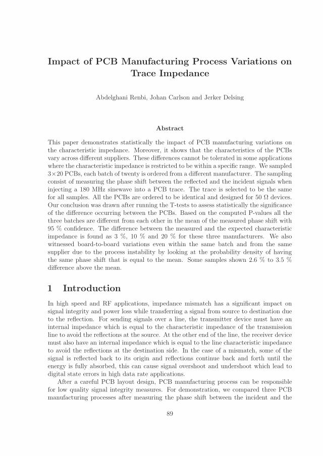
Impact of PCB Manufacturing Process Variations on
Trace Impedance
Abdelghani Renbi, Johan Carlson and Jerker Delsing
Abstract
This paper demonstrates statistically the impact of PCB manufacturing variations onthe characteristic impedance. Moreover, it shows that the characteristics of the PCBsvary across different suppliers. These differences cannot be tolerated in some applicationswhere the characteristic impedance is restricted to be within a specific range. We sampled3×20 PCBs, each batch of twenty is ordered from a different manufacturer. The samplingconsist of measuring the phase shift between the reflected and the incident signals wheninjecting a 180 MHz sinewave into a PCB trace. The trace is selected to be the samefor all samples. All the PCBs are ordered to be identical and designed for 50 Ω devices.Our conclusion was drawn after running the T-tests to assess statistically the significanceof the difference occurring between the PCBs. Based on the computed P-values all thethree batches are different from each other in the mean of the measured phase shift with95 % confidence. The difference between the measured and the expected characteristicimpedance is found as 3 %, 10 % and 20 % for these three manufacturers. We alsowitnessed board-to-board variations even within the same batch and from the samesupplier due to the process instability by looking at the probability density of havingthe same phase shift that is equal to the mean. Some samples shown 2.6 % to 3.5 %difference above the mean.
1 Introduction
In high speed and RF applications, impedance mismatch has a significant impact onsignal integrity and power loss while transferring a signal from source to destination dueto the reflection. For sending signals over a line, the transmitter device must have aninternal impedance which is equal to the characteristic impedance of the transmissionline to avoid the reflections at the source. At the other end of the line, the receiver devicemust also have an internal impedance which is equal to the line characteristic impedanceto avoid the reflections at the destination side. In the case of a mismatch, some of thesignal is reflected back to its origin and reflections continue back and forth until theenergy is fully absorbed, this can cause signal overshoot and undershoot which lead todigital state errors in high data rate applications.
After a careful PCB layout design, PCB manufacturing process can be responsiblefor low quality signal integrity measures. For demonstration, we compared three PCBmanufacturing processes after measuring the phase shift between the incident and the
89

90 Paper B
reflected signals when injecting a 180 MHz sinewave into a PCB trace. Each process ispresented by 20 PCB samples of the same design. We also evaluated the process stabilityfor each manufacturer [1].
2 Related Work
The impacts of the fabrication process have been studied in [2], the focus was aboutthe impact of copper surface roughness and the moisture absorbed by the pre-preg onthe conductive and the dielectric loss respectively. Copper surface roughness is achievedby the adhesion promotion treatment. As the copper roughness worsens the conductiveloss, a balance between the mechanical reliability and the conductive loss is needed, themechanical reliability refers to the mechanical joint between the copper surface and thepre-preg which is ensured by the copper surface roughness.The other outcome of the research is that the moisture absorbed by the pre-preg before thelamination process degrades eternally the dielectric loss. Precautions are to be taken inaccount to achieve good storing conditions which minimize pre-preg moisture absorption.
In [3], where the author studied the impact of PCB weave on the skew. Looking atthe substrate from the weave level, the traces lie on non-homogenous dielectric, thereforesome traces might be on the top of a substrate where the epoxy resin is dominant andothers might be on the top of the substrate where the fiber glass is dominant, this causesthe wave to propagate with different speeds within the same board and therefore a skewbetween an equal length traces. The weave can lead to 5 % to more than 10 % variationin propagation delay within identical physical length. The percentage of glass to epoxyand weave style have a significant impact on dialectic constant and therefore on thepropagation delay.
PCB fabricators are facing big challenges to meet good quality for high frequencyrequirements, short pulses technique has been published in [4] for PCB manufacturersto assess the produced PCB trace in term of frequency dependent propagation constant,this can increase the confidence of the manufacturers about their quality by running fewtests.
3 PCB manufacturing variations and characteristic
impedance
3.1 Characteristic impedance
Generally, the characteristic impedance is a complex number with a resistive and reactivecomponent. It is a function of the frequency of the applied signal, and is independant tolength. Based on the telegrapher’s equations the characteristic impedance is:
Z0 =
√R + jLω
G+ jCω(1)

3. PCB manufacturing variations and characteristic impedance 91
Where R is the resistance per unit length, L is the inductance per unit length, G is theconductance of the dielectric per unit length, C is the capacitance per unit length, j isthe imaginary unit, and ω is the angular frequency.
Talking about the same length of a PCB trace. At the same frequency, any change inthe input impedance signifies a change in the capacitance for that specific length whichformed by the trace and the ground plane with the insulator. Any change in per unitlength capacitance signifies a change in the characteristic impedance. By measuring thechanges in the input impedance of a trace we will also be measuring a change in thecharacteristic impedance.
3.2 Possible manufacturing variations
There exist several variations that can occur during volume production of PCBs, many ofthese variations will affect the characteristic impedance of the trace and may fall outsidethe accepted range. Figure 1 shows a typical PCB trace which is called a microstrip line.
Figure 1: PCB trace.
The ratio of the conductor width Wh
to the distance from the power plane h plays animportant role in controlling the impedance, εr which is the dielectric constant of thematerial that separates the trace from the power plane is also an important factor. Thesetwo work together to form the characteristic impedance described in the equation 1.
Variations in etching affect the width of the trace which results in changes in the area,typically the tolerance on trace width is ±10 %. The processes used for creating the coreFR-4 and for pressing the pre-preg layers of FR-4 are also inexact.
The thickness of a trace is determined by the employed copper foil and is rarelyspecified with a tolerance, mostly is considered constant. The dielectric constant may bein the range of 4.2 to 4.4 when is intended to be 4.3.
In practice, a PCB trace is not rectangular as intended to be. Process differences

92 Paper B
between suppliers, between different batches of PCBs or even within a single batch fromone supplier, can cause significant variations in the shape and smoothness of a traceperimeter.
All these variations will enforce the characteristic impedance to be within a rangewhile is expected to be 50 Ω [1].
4 Methodology
As mentioned in section 3.1, Any change in per unit length capacitance signifies a changein the characteristic impedance. By measuring the changes in the input impedance of atrace, see figure 2, we will also be measuring a change in the characteristic impedance.To measure the change in the input impedance we measured the phase shift of thereflected signal from the input impedance formed by the PCB trace after injecting a 180MHz sinewave signal.
The measurements have been performed in a stable environment and any significantdeviations in the measured values have been repeated several times to ensure the validityof data. The frequency has been chosen to be specifically 180 MHz for adjusting themeasuring device to its highest sensitivity, this frequency depends on the coaxial linelength which has been employed for signal transmission.
Figure 2: Employed trace for process evaluation. It is designed for 50 Ω devices.
Following table represents the collected data from the three manufacturers samples.

5. Analysis 93
Table 1: Phase shift data.PCB M1 M2 M3
samples
1 2.33 2.27 2.302 2.34 2.27 2.323 2.32 2.27 2.324 2.33 2.27 2.305 2.31 2.26 2.316 2.32 2.27 2.317 2.32 2.25 2.338 2.34 2.26 2.299 2.42 2.27 2.3210 2.34 2.27 2.3211 2.33 2.27 2.3212 2.32 2.27 2.3813 2.34 2.28 2.3214 2.34 2.27 2.3115 2.34 2.26 2.3216 2.34 2.26 2.3817 2.34 2.26 2.3018 2.34 2.26 2.3219 2.35 2.27 2.3120 2.35 2.26 2.32
5 Analysis
5.1 T-test and P-value
In statistical analysis, the most commonly used procedure to determine whether or nottwo populations have different mean values on some measure is the T-test procedure.Let A and B be the two populations in question and M is the measure. We might doa research to clarify the hypothesis that A and B are different regarding the measureM. We run an experiment or a questionnaire to measure some samples of M in bothof populations. We assume that the null hypothesis is true, which means that there isno difference between A and B on the measure M. What will happen if we observe adifference in the mean values of M in both populations? How will we decide that thepopulations A and B are really different?

94 Paper B
The T-test allows us to answer the above questions by computing the P-value thatindicates the strength of the evidence against the null hypothesis. If the P-value is lessthan 0.05, the null hypothesis is to be rejected and the difference is statistically significant.If the P-value is greater than 0.05, the difference between the two populations is notstatistically significant.
5.2 Significance of mean differences
Based on the results which are shown in table 1, we can see clearly that there is adifference between the PCBs. By looking at table 2 we may capture an image about thesignificance of the difference between the three batches. To draw a conclusion whether ornot the batches of the PCBs are physically different from each other, we ran the T-teststo assess statistically the significance of the difference occurring between the batches. Weposed an hypothesis H0, which claims that each batch has an equal mean μ as the otherone. According to the computed P-Values, which are shown in table 3, all these threebatches are different and the hypothesis is rejected with less than 5 % chance.
Table 2: Phase shift mean and StDev values.Manufacturer Phase shift mean μ StDev
M1 2.338 0.02215M2 2.266 0.00681M3 2.320 0.02271
Table 3: P-values with 95 % CI for mean difference.Mean P-Value 95 % CI for
difference mean difference
μ1 − μ2 0.000 0.06163 , 0.08237μ1 − μ3 0.024 0.00269 , 0.03331μ2 − μ3 0.000 -0.06530 , -0.04270
5.3 Characteristic impedance verification
In this section, we evaluate the expected quality of these three batches of PCBs. Thespecified requirement of the PCB trace is to be 50 Ω as the characteristic impedance. Forthis we performed the scattering parameters extraction using a vector network analyzerand computed the characteristic impedance within a range of frequency of 100 MHz upto 1.5 GHz. To compute the characteristic impedance with sufficient accuracy, the de-

5. Analysis 95
embedding procedure has been taken into the consideration to remove the effect of theconnector which we used for the measurement:[
A BC D
]DUT
=
[A BC D
]−1Port
×[A BC D
]Device
(2)
The device matrix represents the matrix of the cascaded connector with the trace asshown in the upper part of figure 3. The port matrix represents the matrix of theconnector. The DUT matrix represents the matrix of the trace as they are separated inthe lower part of figure 3. The complete followed procedure is well described in [5].
Figure 3: Device, Port and DUT.
After computing the ABCD matrix of the trace which is refereed as device under test(DUT), directly we computed the characteristic impedance which can be written as:
Zc =
√A
C
B
D=
√B
C(3)
when the system trace is symmetric as it is in our case.Geometrically, the trace has been designed to be 49.8 Ω with 4.2 as the FR-4 epoxy
dialectic constant. According to the results shown in the figure 4, The process of M1led to the closet characteristic impedance as intended to be, while the process of M3resulted on a moderate quality, on the other hand a significant difference is shown in thecharacteristic impedance of trace from M2, this latest might lead to unexpected behaviorin high frequencies applications.
5.4 Glass cloth weave
After the dissolving process of the epoxy , the weave of the glass cloth illustrated in figure5 used by M1, M2 and M3 seems to be similar therefore the weave cannot be the main

96 Paper B
5 10 15
x 108
40
45
50
55
Frequency (Hz)
Zc
(Ohm
)
M1M2M3
Figure 4: Characteristic impedance from the three processes.
(a) M1 (b) M2 (c) M3
Figure 5: Glass cloth after the dissolving process
contributor to difference obtained in the phase shift results especially when the traceis 1 mm wider. We could expect some differences due to the cloth weave in the PCBused by M3 if the trace width is much smaller that the bundle width where it mightlie on different dielectric constant of the substrate composite. This comparison put thethickness of the substrate and the tolerances of the dielectric constant of both epoxy andglass in a good position of the source of the difference in the resulted phase shift values.

5. Analysis 97
5.5 Stability analysis
Figure 6 shows the probability density of measuring the same phase shift between thereflected and the incident signal been applied to the trace within the batch of PCBs fromM1, M2 and M3. The phase shift is represented here by a voltage quantity according tothe measuring device.
2.25 2.3 2.35 2.40
10
20
30
40
50
60
Phase Shift
Pro
babi
lity
Den
sity
M1M3M2
M=2.226StDed=0.006806N=20
M=2.32StDed=0.02271N=20
M=2.338StDed=0.02215N=20
Figure 6: Probability density of the phase shift.
The process of M2 is characterized by the highest stability as all the samples shownalmost similar phase shift with a very small standard deviation of σ = 0.006806, thus theprocess is a good example for nearly identical PCBs production. On the other hand, bothprocesses of the other two manufacturers are less stable. M1 process led to a phase shiftstandard deviation of σ = 0.02215, one sample of its population shown an increase by

98 Paper B
almost 3.51 % above the mean. This sample has been repeated several times to ensure theconfidence of our conclusions. This confirms what we discussed in section 3.2 about theprobable difference within a batch of PCBs which are produced by the same process. Thebiggest factor candidate which might be responsible of this difference could be thicknessof the sample due to some mechanical variations while pressing the pre-preg layers. M3process is the least stable with a standard deviation of σ = 0.02271 in the phase shift.There are two samples which are notable to be above the mean μ = 2.32 of the phaseshift by 2.6 %. This also part of the possible variations within the same produced batch.
Figure 7 shows the probability density of measuring the same phase shift betweenthe reflected and the incident signal been applied to the trace within the all the batchesof PCBs from all manufacturers. The phase shift is represented by a voltage quantityaccording to the measuring device.
2.2 2.3 2.40
2
4
6
8
10
12
Phase Shift
Pro
babi
lity
Den
sity
M=2.308StDev=0.03593N=60
Figure 7: Probability density of the phase shift mean in design from all three manufacturers.
According to the graph, the standard deviation of the phase shift σ = 0.03593 gothigher as compared to the one we obtained within the same process, this explains that

99
the process are different from each others and one should consider whether or not thedifference can be tolerated while changing the PCB supplier for a specific design [6].
6 Conclusion
Statistical analysis shows that PCB characteristic impedance might be out of the tol-erated range of a specific RF design due to the instability of the design process. Forextremely critical RF applications, extra caution need to be considered when orderingfrom different PCB suppliers. Statistical analysis can be very useful to evaluate PCBvendors quality before making big orders.
References
[1] C. F. Coombs, Printed Circuits Handbook, 5th ed. McGraw-Hill Professional Pub-lishing, 2007, ch. 10.
[2] J. Lin, A. Huang, O. Huang, and S. Chen, “A case study of the impact of fabricationprocesses on pcb broadband electrical characteristics.” International Symposium onMicroelectronics, 2009.
[3] S. McMorrow, “The impact of pcb lmainate weave on the electrical performance ofdifferential at multi-gigabit data rates,” 2005.
[4] R. K. John DiTucci, “Production measurement of frequency dependent attenuationand phase constant of pcb traces.” IMAPS, 2009.
[5] S. H. Hall, Advanced Signal Integrity for High-Speed Digital Designs, 1st ed. Wiley-IEEE Press, 2009, ch. Network Analysis for Digital Engineers, pp. 395–400.
[6] D. C. Montgomery, Design and Analysis of Experiments, 7th ed. Wiley, ch. 2.

100

Paper C
Reflection phase shift for PWB andPCBA Production Testing
Authors:Abdelghani Renbi and Jerker Delsing
Reformatted version of paper originally published in:Journal of Microelectronics and Electronic Packaging
© 2012, IMAPS, Reprinted with permission.
101

102

Reflection phase shift for PWB and PCBA
Production Testing
Abdelghani Renbi and Jerker Delsing
Abstract
Printed wiring board (PWB) and printed circuit board assembly (PCBA) testing is partof the electronics production, which has a great impact on the profitability. Always highthroughput and low cost testing is needed but for high quality and reliability. Bareboard testing is vital before components loading. Defects after the PWB manufacturingprocess are possible such as opens, bridges, near-opens, near-bridges and characteristicimpedance mismatches due to process variations and compounding raw material toler-ances. Moreover, defects might cost about ten times more when detected in the next testphase, another motivation for unpopulated board test is loading expensive componentson a set of defective boards might be economically catastrophic. Flying probe systems,which were developed in late 1980’s are commonly used and favorable to perform bareboard isolation and continuity testing, especially when the volume is not big enough tojustify bed of nails purchase. Flying probe system performance for a given bare boarddepends on the test algorithm, the mechanical speed and the number of probes. Toreduce the cost on expensive test probes and probe maintenance and to accelerate thetest time, this paper presents a new and cost efficient approach to test unpopulated andpopulated board with open sockets, using a single probe. Specifically, a coaxial probeinjects one frequency signal into the PWB trace, the phase shift between the reflectedsignal from the trace and the incident wave is detected and compared with the nominalvalue, which has been captured from a defect free board, which already underwent directcontinuity and isolation testing. By applying this test solution to bed-of-nails equip-ment, we will be reducing 50 % of the probes, on the other by employing this solutionto flying probes system with two probes, for a given design with NI isolated traces andNA adjacent pairs we will be reducing the number of tests from (NI+NA) tests to NItests as isolation and continuity are performed in one go. Flying probes system involvesmechanical movements, which dominate the test time, by reducing the number of themechanical movements we will be increasing dramatically the test throughput. The con-ducted experiments have shown a good feasibility for practical use in the Automatic TestEquipment (ATE) for PWB and PCBA testing. At the highest sensitivity of the phaseshift detector, the prototyped tester is capable to distinguish between a defective anderror free board with significant margins in case of defects such as opens, DC and RFbridges, exceeded and different width lines. The margin in the measurement betweena defective and a correct board, which depends on the type of the defect is about 7 %to 68 %. In case of loaded board testing, the approach is capable in detecting openswith important margins, our test cases shown 40 % and 33 %, which makes it a strong
103

104 Paper C
candidate approach to be applied officially to PCBA testing where probing is feasible.The approach can be applied to the complete layout or to boost the test strartegy wherethe applied test solutions are not covering 100 % of the possible defects.
1 Introduction
Flying-probe systems have joined the mainstream in late 1980’s and become popularfor their ability of performing ICT without the need of expensive bed of nails and theirability of fine pitch access [1]. The main factor, which drove the electronics manufacturersto use flying probe systems is cost-effective testing especial when the volume does notjustify bed-of nails purchase, however flying-probe systems are prone to slow performancedue to the mechanical movements of the probes. The success of flying probe-systems isrelated to their success in entering in high volume productions, however this still openissue to the electronics manufacturers. In the past costumers have not been pressuringbare boards suppliers for electrically tested products, due to the evolution of small sizeelectronics, this tradition has already started changing, today’s costumer is more likelyto buy tested products. It has been reported that failed bare board represent 5 % insingle sided boards, 5 % to 10 % in plated-through hole boards and any value between10 % and 100 % in multi-layers boars [2].
2 Related work
Apart from the direct test methods for bare boards, the author of [3] has mentioned thatthere exist few bare board test methods, which are unique to the direct electrical tests.Capacitive and electromagnetic coupling is the main principal. He stated that thesemethods are reliable when detecting DC shorts and opens, but may be less effective indetecting distributed high resistance connections. Capacitive measurement, which wasstated is based on measuring the ratio of the variation of time and the voltage levelwhen a constant current is flowing into a capacitance trace. More over nothing has beenpublished explicitly within the bare board test methods. It seems that there is a greatneed of an academic contribution in this area.
To increase the test coverage in designs where both Boundary-Scan and non-Boundary-Scan devices, passive components and empty sockets are mixed. Stephen Sunter and Ken-neth P. Parker have presented in [4] the implementation of an experiment where theydemonstrated that the capacitive sensing concept can be combined with the Boundary-Scan for new test standards to cover passive components and empty sockets. The conceptbeauty is the use of the Boundary-Scan signals.
3 Theoretical Background
In this section we will discuss three topics in microwave theory, which build the groundof understanding the workhorse of our prototyped idea for the single probe tester.

3. Theoretical Background 105
3.1 Wave Reflection
In the field of microwave when the physical length of the transmission line is much longerthan the wavelength, the transmission is not trivial as it is in the circuit theory. Fora wavelength λ and a physical length L, the voltage and currents can vary in phaseand magnitude over its length and the transmission line becomes an influencing part ofthe magnitude and phase of the received signal. These variations over the line becomesignificant when L > λ
10. Figure below shows an transmission line employed to carry
a signal from a source E with an internal impedance ZS to a destination load with animpedance ZL. The transmission line is characterized by its characteristic impedanceZC , its wave velocity Vp and its length L.
Vr ZL
ZS
Vi
ZC, Vp, L
xL0
E
Figure 1: Reflection in Transmission Line
Below are the solutions to the wave equations in a transmission line, which relate theback and forward waves.
V (X) = Ae−γX +Be+γX (1)
I(X) = Ae−γX
ZC
− Be+γX
ZC
(2)
where γ is the propagation constant of the transmission line and A and B can be writtenas follows:
A =ZC(ZC + ZL)e
+γLE
(ZC − ZS)(ZC − ZL)e−γL − (ZC + ZS)(ZC + ZL)e+γL(3)
B =ZC(ZC − ZL)e
−γLE
(ZC − ZS)(ZC − ZL)e−γL − (ZC + ZS)(ZC + ZL)e+γL(4)
For the transmission line in figure 1, the voltage reflection coefficient at the load isdefined as the complex ratio of the reflected voltage to the incident voltage, which canbe written as:
ΓL =ZL − ZC
ZL + ZC
= |ΓL|ejθΓ (5)

106 Paper C
Considering a lossless transmission line, where the propagation constant γ = jβ anda source with an internal impedance ZS, which is equal to the characteristic impedanceof the line ZC .A and B become: A = 1
2E and B = 1
2E |ΓL|ej(θΓ−2βL)
And equation 1 becomes :
V (X) =1
2Ee−jβX +
1
2E|ΓL|ej(θΓ−2βL)e+jβX (6)
The voltage along the line is superposed by two parts, the incident voltage, which isin the left side and the reflected voltage, which is in the right side of equation 6.By keeping the measurement position X and the characteristics of the transmission lineconstant, the phase shift between the incident and the reflected signal will depend onlyon the phase angle of the reflection coefficient at the load, which can be written as:θΓ = θ(ZL−ZC) − θ(ZL+ZC), where θ is the phase angle [5]. The trigonometric form of thevoltage at X=0 can be written as :
V (0, t) =1
2E cos(ωt) +
1
2E|ΓL| cos(ωt+ θΓ − 2βL) (7)
3.2 Frequency Mixing
Frequency mixers are mostly used in applications, when phase shift information is re-quired. The principal upon which phase shift detection rests is that mixing two signalswith an equal frequency results in a DC voltage after a proper filtering of higher fre-quency components as shown in figure 2. Mathematically, a frequency mixer output canbe described as:
Vf = A cos(ω1t+ φ1)B cos(ω2t+ φ2) (8)
which reminds us of an AM modulator output. If the input signals have the same fre-quency 2πω we simply modify the function from an AM modulation to a phase detection.
Vf =AB
2[cos(φ1 − φ2) + cos(2ωt+ φ1 + φ2)] (9)
By filtering out the higher frequency component, Vf will be only a function of the phaseshift between the two input signals.
Vf =AB
2cos(φ1 − φ2) =
AB
2cos(Δφ) (10)
Where Vf is the output voltage of the mixer, A cos(ω1t + φ1) is the signal at the inputLO and A cos(ω1t+φ1) is the signal at the input RF . Figure 2 shows that the maximumand the minimum of the function appear at Δφ = 0 and Δφ = π respectively, based on

3. Theoretical Background 107
LO
RFπ
Low passfilter
Vf
Vf ΔΦ
δΦ
Figure 2: Principal of phase shift detection
the implementation the term AB2cos(Δφ) might inherit a negative sign and therefore the
maximum and minimum will exchange the positions. According to the plotted fuctionin figure 2 we can also remark that the highest sensitivity of the phase shift detectorcan be achieved at the linear region of the plot, which is around Δφ = π
2, let us say
the linear region is determined by the segment whose X coordinates are π2± δφ. This
segment appears at each nπ2± δφ, where n is an odd integer. The sensitivity
Δ Vf
Δφcan be
improved by increasing the maximum of the output function, the higher maximum thebetter sensitivity will be [6].
3.3 Reflection Detection
Directional couplers are commonly deployed for coupling a proportion of a traveling wavein a transmission line out through another port. The concept behind is that by settingtwo transmission lines close enough to each others an amount of power will be travelingin the neighborhood line. Figure 3 shows a 4-port directional- coupler, which can be used
3
1
4
2Directional coupler
Figure 3: Directional coupler
to sense the reflected signal at the port 4. It consists of 4 ports: Port (1), which refersto the main device input, Port (2), which refers to the main device signal output, port(3), which is coupled with Port (1) for the incident signal and finally the isolated Port(4), which is coupled to the port (2) for sensing the reflected signal. Figure 4 in section

108 Paper C
4, shows how the directional coupler is involved in our tester schematics, it can be seeneasily that the above description of the directional coupler matches with the purpose.
4 Methodology
The single probe tester uses the notion of voltage reflection, which is described in insection 3.1 as a main vehicle to detect differences between a correct PWB trace and adefective one. The source of the difference will be presented in the phaser of the reflec-tion coefficient, which depends on the load. There are three main parts in the tester,
Transmission Line
PCB Traceas ZL
Amp
AmpAmp
Directional Coupler
FrequencyMixer
SignalConditioning ADC Comparaison
UnitFail/PassDisplay
VCO
50Ω
Figure 4: Schematic of the Single Probe Tester
the directional coupler, which senses the reflected signal and the frequency mixer, whichdetects the phase shift between the incident and the reflected waves. As the test natureis referential, the comparison unit stores the phase shift references of each trace of anerror free board for comparison with the unit under test and therefore falling or passingthe test. Considering a short microstrip line as a unit under test, the input impedanceZL can be written as follows using one π cell, which is illustrated in figure 5.
ZLCTrace/2
LTrace
CTrace/2
Figure 5: A π cell of a lossless microstrip line

5. Experiment and Simulation 109
ZL =j(1− lcω2)
lc2ω3 − 2cω(11)
If the characteristic impedance of the transmission line is 50 Ω, we can write:
θΓ = 2arctan[1− lcω2
100cω − 50lc2ω3] (12)
where c = CTrace
2and l = LTrace. Theoretically any change in a trace shape or dielectric
thickness and characteristics will be seen in the phase shift described by the above equa-tion.In this work we refer to one bare board design, which consists of few 50 Ω traces withW=1 mm, h=0.5 mm, t=18 um and FR4 substrate, where W is the width of the trace,h is the height of the inserted substrate between the trace and the ground plane and t isthe thickness of the cooper foil. To model the possible alarming production defects, weintroduced an open, an RF bridge, a DC bridge and a weaker trace in our design andeach defective board contains one defect only, see figure 6.
Open DC bridgeRF bridge
Smaller width
Figure 6: Reference bare board with some defect locations.
5 Experiment and Simulation
5.1 Simulation
Knowing that the board traces will be tested only at the frequencies, which lead to thehighest sensitivity of the phase shift detector, in other words, the frequencies, which leadto ±nπ
2. We performed S11 simulations on each correct and defective trace separately.
The effect of 0.45 m length and 2.1 × 10⁸ m/s propagation speed of the probe on thetotal phase shift has been added manually after measuring the propagation speed of the

110 Paper C
transmission line of the probe. Equation 7 describes the total phase angle of the reflectedsignal. The phase angle of S11 is totaly linear with a negative slope. From the linearfunction relating the frequency and the phase angle of S11 of the correct trace we extractedthe frequencies, which lead to the odd multiples of the part, which is due to the probelength and speed. On the other hand we extracted the phase angle of those frequenciesin the function relating the frequency and the phase angle of S11 of the defective trace,then the difference in the phase shift can be evaluated. It is clearly seen that the biggern is the more visible the defect is. The following tables summarize the collected data ofthe phase shift information for the different introduced defects, ΦC and ΦD refer to thephase shift, which corresponds to the correct and the defective trace respectively. Figure8 shows that the RF bridge defect is characterized by the smallest margin followed by theopen defect as the test point is far from the location of the break, on the other hand ifthe test is performed at the side, which is closer to the break, the margin will be greater.Of course we do not want to double test the trace as the original goal is to improve thetest time and the test maintenance cost, increasing the factor n and improving the phaseshift sensitivity is the key solution for this kind of limitations. Nevertheless we will seethat this margin is visible enough at the voltage level as the test was ran at the highestsensitivity of the phase shift detector.
Table 1: Phase shift data for different defects when n=3.Defect Test ΦC ΦD Δ
frequency
Open 151 MHz -270◦ -265◦ 5◦
DC Bridge 145 MHz -270◦ -309◦ -39◦
RF Bridge 143 MHz -270◦ -271◦ -1◦
Smaller 155 MHz -270◦ -247◦ 23◦
Width
Table 2: Phase shift data for different defects when n=5.Defect Test ΦC ΦD Δ
frequency
Open 251 MHz -450◦ -440◦ 10◦
DC Bridge 242 MHz -450◦ -514◦ -64◦
RF Bridge 239 MHz -450◦ -452◦ -2◦
Smaller 258 MHz -450◦ -411◦ 39◦
Width

5. Experiment and Simulation 111
Table 3: Phase shift data for different defects when n=7.Defect Test ΦC ΦD Δ
frequency
Open 351 MHz -630◦ -615◦ 15◦
DC Bridge 338 MHz -630◦ -717◦ -87◦
RF Bridge 335 MHz -630◦ -634◦ -4◦
Smaller 362 MHz -630◦ -577◦ 53◦
Width
0 2 4 6
x 108
-800
-600
-400
-200
0Open
CorrectDefective
0 2 4 6
x 108
-800
-600
-400
-200
0DC Bridge
CorrectDefective
0 2 4 6
x 108
-800
-600
-400
-200
0RF Bridge
CorrectDefective
0 2 4 6
x 108
-800
-600
-400
-200
0Smaller Width
CorrectDefective
Figure 7: Simulated phase shift in ◦ versus the frequency in Hz for the four introduced defects.
5.2 Experiment
In this section we present some results achieved by the prototype, which was implementedbased on the schematic illustrated in figure 4. The experiment consists of employing theprototype for bare board testing where we compared the phase shift between the incidentand the reflected signal in the correct and the defective boards, which we described insection 4, each defect has been implemented separately in one board. Keeping in mind

112 Paper C
020406080
100
Open DC Bridge RF Bridge SmallerWidth
n=3 n=5 n=7
Figure 8: Absolute value of the phase shift difference in ◦
that the board has to be tested cheaply, this led to some limitations on the testingfrequency when we employed only the first odd multiple frequency, which is able to set theoffset phase shift to -270◦ for the highest sensitivity as explained in section 3.2. Table 4
Table 4: Phase shift data for different defects.Defect Test ΦC ΦD Δ
frequency
Open 188.5 MHz -270◦ -313◦ -43DC Bridge 182 MHz -270◦ -231◦ 39RF Bridge 177 MHz -270◦ -266◦ 4Smaller 191 MHz -270◦ -312◦ -42Width
Table 5: Phase shift data for different defects (voltage).
Defect Test VC VD Δ
frequency
Open 188.5 MHz 1.7 2.87 68 %DC Bridge 182 MHz 1.7 0.63 63 %RF Bridge 177 MHz 1.7 1.58 7 %Smaller 191 MHz 1.7 2.85 67.5 %Width
contains the measured phase shift data in the correct and the defective board. The phaseshift values include already the phase introduced by a 50 Ω transmission line of the testingprobe whose length is 45 cm, the propagation speed in the transmission line is 70 % of thespeed of light in the vacuum. The Simulation and experiment results agree moderatelywith each others due to several reasons which we do not discuss explicitly here in this

5. Experiment and Simulation 113
paper. One of those reasons is the interference noise during the experiment, which is notcovered in the simulation medium, the other one also is the ground wire connecting theprobe with the board under test, which introduces at least a small inductance. We suggestfor the final product that the ground wire has to move with a constant path for eachtrace, this way the wire will keep the same inductance at every board. Another sourceof disagreement between the simulation and the measurement is the output equation ofthe phase shift detector which we suppose that is nearly ideal with a null offset voltage,which might not be true. We also suspect that the differences in the physical structureand the characteristics of the board, which we used in the simulation such as variationsin the thickness of the substrate or in the dielectric constant.Table 5 presents the defects visibility at the voltage level after some signal conditioningfor the processing unit. The voltage is indicated by VC and VD for the correct and thedefective traces.
5.3 Sensitivity analysis using MATLAB model
In addition to simulation, another alternative approach to determine the test frequenciesfor better sensitivity before programming the control unit which adjusts the frequency ofeach trace is the lumped model of the microstrip line illustrated in 5 with the help of thetotal phase shift described by equations 13 and 12. To determine the lumped elementone can use the numerical methods as long as the approximations in the formulas arevalid and match within the relative size of the structure. For the highest sensitivity thefollowing condition needs to be true:
θΓ − 2βL = ±π
2(13)
Which implies:
tan(±π
4+
2πfL
Vp)︸ ︷︷ ︸
Part1
− (1− lc(2πf)2)
100c(2πf)− 50lc2(2πf)3))︸ ︷︷ ︸
Part2
= 0 (14)
Employing this alternative to the error-free trace in the board, which is 56 mm long andusing a graphical solution to solve the above equation, figure 9 shows the intersectionof the two parts of the above equation where the condition is true. The frequencies ofintersection are to be the test frequencies for that trace in order to achieve the highestsensitivity. We remark that these results agree with the frequencies, which we determinedin the simulation section.
5.4 Stability analysis of the device
During the measurements, it has been noticed some random deviations in the measure-ment are appearing time to time in which we suspect the near field around the probeespecially when the probe is held by the human hand or is surrounded by the powersupply cables. The single probe tester is tended to be piloted by an arm robot in a stableand shielded environment where the mechanical movements are constant from test to test

114 Paper C
Figure 9: Test frequencies for 56 mm long trace
of each trace, this way there will no source of deviations. To inspect the device stability,we took 10 samples for each defect and drawn the probability density function, refer totable 6 and figure 10.
Table 6: Phase shift voltage samples for stability test purpose.Open Smaller Width DC Bridge RF Bridge
2.859 2.8 0.639 1.5682.86 2.865 0.634 1.5422.862 2.776 0.632 1.5472.866 2.886 0.629 1.6142.867 2.879 0.63 1.6132.858 2.882 0.634 1.612.861 2.862 0.634 1.5772.858 2.859 0.633 1.5662.886 2.85 0.633 1.5972.863 2.82 0.632 1.587
5.5 Process summary
Following flowchart describes high level algorithm to be followed to test a bare boardafter the production phase using the single probe tester, which is discussed in this paper.
6. Process stability and characteristic impedance verification 115
1.4 1.6 1.8 20
5
10
15
20RF Bridge
M=1.5821StDev=0.0265N=10
0.62 0.64 0.66 0.680
50
100
150DC Bridge
M=0.6330StDev=0.00271N=10
2.6 2.7 2.8 2.9 30
2
4
6
8
10
12Smaller Width
M=2.8479StDev=0.0372N=10
2.8 2.85 2.9 2.950
50
100
150Open
M=2.8614StDev=0.00313N=10
Figure 10: Probability density versus the phase shift voltage with 95 % CI.
6 Process stability and characteristic impedance ver-
ification
As addressed in [7], It is also important to test few samples of PWBs to check the processstability by measuring the input impedance of a trace or its characteristic impedance,this kind of test can be done by the manufacturer before any required process tuning,or can be performed by the client in case of evaluating the quality of the ordered boardsfor the quality of the process of different vendors before going for high volume orders.In addition to the process variations impact on the phase shift measure within the samebatch, figure 14 shows also the difference that can occur between the PWB suppliers.
Characteristic impedance mismatch has a significant impact on signal integrity andpower loss while transferring RF and high speed signals between a source and a destina-tion, The mismatch causes back and forth signal reflections between devices and thereforesignal overshoots and undershoots resulting in signal reading errors. Testing the charac-teristic impedance correctness for the traces, which are designed to carry high speed andRF signals is vital, after the manufacturing process the characteristic impedance can beout of the expected range due to process variations and compound material tolerances.Several factors control the characteristic impedance of the trace such as the shape ofthe edges, which can be rounded, rectangular or trapezoidal depending on the etchingprocess, the dimensions of the traces including the width and the thickness, the isolatorrelative permittivity and its thickness. Figure 12 shows all these factors. Typically theinsulator, which is inserted between the trace and the ground plane is an FR-4 insulator,

116 Paper C
Extract the measurement tolerances based onset of samples of each trace in a set of bare
boards (Underwent direct continuity andisolation testing)
Program the Test Unit to adjust the VCO to thefrequency that corresponds to nx π/2
Determine the test frequencies, which leadto nx π/2 phase shift for each trace (usingexperiment, simulation or lumped model),
preferably using experiment on a prototypePCB with the test environment.
Pass or Fail based on the tolerances
Start
Figure 11: Bare board test algorithm using single probe tester
Figure 12: Factors, which control the characteristic impedance of a trace.
which is consists of glass fiber weave enforced by the epoxy resin, thus the traces inPWB lies on non-homogenous dielectric where some traces might be on the top of a sub-strate where the epoxy resin is dominant and others might be on the top of the substratewhere the fiber glass is dominant, see figure 13 this causes variations in the characteristicimpedance between the traces even in the same PWB [8], Figure 14 illustrates the prob-ability density of the phase shift measure, which represents the characteristic impedanceat one frequency on a trace, according to the figure, the characteristic impedance is notexactly the same within 20 samples, these variations vary between the three manufac-turers M1, M2 and M3. The question is how tolerated this range can be? [7] discusses

6. Process stability and characteristic impedance verification 117
this issue thoroughly and provides a quick solution for testing the correctness of thecharacteristic impedance using the phase shift method presented in this paper.
Figure 13: A case where the dielectric is not homogenous. The top trace lies on the dielectricwhere the epoxy is dominant, while the bottom trace lies on the part of the dielectric where theglass is dominant.
2.25 2.3 2.35 2.40
10
20
30
40
50
60
Phase Shift
Pro
babi
lity
Den
sity
M1M3M2
M=2.226StDed=0.006806N=20
M=2.32StDed=0.02271N=20
M=2.338StDed=0.02215N=20
Figure 14: Probability density of the phase shift, which represents the characteristic impedance.

118 Paper C
7 Loaded board testing
This time, the load ZL is more complicated than a simple trace, Let ZL be a generalcomplex quantity, which depends on the network layout, the attached components and thetest frequency, ZL = a+ jb. The reflection coefficient at the load ΓL = ZL−ZC
ZL+ZC= |ΓL|ejθΓ .
where:
ΓL| =√(a2 + b2 − Z2
C)2 + 4b2Z2
C
(a+ ZC)2 + b2(15)
and
θΓ = arctan(b
a− ZC
)− arctan(b
a+ ZC
) (16)
Any change in the real and the imaginary parts causes a change in the phase shiftbetween the incident and the reflected signals. Due to the infinite number of the possiblelayout structures that can be connected to an IC pin or an SMD pad, one cannot makeany general analysis for sensitivity and defect margin analysis without knowing the loadimpedance as complex quantity that the probe sees. To achieve high sensitivity as it hasbeen done with the PWB, One can always collect the frequencies, which lead to ±π
2by
measurements on an error-free prototype.One typical case, which can be faced most often in PCBA is a two ICs connected
together via a trace. This case proves the approach ability of discriminating the defectswith significant margins while probing on the IC pins for testing. Let IC1 and IC2 beconnected via a trace as shown in figure 15, assuming a case where the output capacitanceof IC1 pin is 2 to 5 pF and the input capacitance of IC2 is 5 to10 pF, for a typical 50Ω trace with 200 μm width and 18 μm thickness on FR-4 substrate whose thicknessis 120 μm. For 5 cm as the maximum trace length (Lengthmax) in the layout, the testfrequency must be smaller than C
10×Lengthmax� 360MHz where C is the propagation speed
in the medium and it is approximately equal to 1.8 m/s when the dielectric constant isassumed to be 4.5. The test frequency condition Lengthmax < λ
10satisfies the validity of
the lumped elements model of the PCBA trace, where λ is the wavelength . By probingon the IC1 pin, the probe will see the load impedance as:
ZL =jN
D(17)
Where N = (1− l(c+ cIC2)ω2),
D = l(c+ cIC1)(c+ cIC2)ω3 − (2c+ cIC1 + cIC2)ω,
c = CTrace
2and l = LTrace. As ZC = 50 Ω of the transmission line, using equation 16, the
phase angle of the reflection coefficient can be written as:
θΓ = −2arctan[N
50D] (18)
Figure 15 illustrates the circuit model for the described scenario for the frequenciessatisfying the condition L < λ
10, where L is the length of the trace. When probing

7. Loaded board testing 119
Figure 15: IC1 and IC2 pins connection circuit model.
Figure 16: Reflection phase shift difference in case of an error-free connection and a connectionwith an open on IC1 pin.
on the top of IC1 pin and in case of an open defect, the probe sees only the outputcapacitance cIC1 and thus θΓ = 2arctan[ 1
50cIC1ω]. Figure 16 shows that the margin phase
shift values are very significant to discriminate the open defects for similar scenarios. Themargins are computed for all the trace lengths between 1mm to 5 cm. Even for 1 mmtrace and big output capacitance of IC1, the margin is still important, which is around

120 Paper C
-30◦.
8 Test examples
In this section we present some results achieved after applying the prototype to a PCBAconnection cases, which include an output of operational amplifier to an ADC and anoutput of a microcontroller, which is connected to buzzer via a capacitor. This kind oftesting can be applied to the complete PCBA nets or boost the test strategy by improvingthe test coverage when the official approach is Boundary-Scan and several nets are notcovered by the Boundary-Scan approach. Table 7 shows the collected measurementsof the open defects for both cases, which have been performed after adjusting the testfrequency, which led to high sensitivity of the mixer, this way we achieved high marginsbetween the error-free and defective connections, which consist of opens between the pinsand the solder joints, refer to the nets indicated by the arrows in figures 17 and 18.
Table 7: Phase shift voltage values of PCBA nets testing, the voltage is indicated by VC andVD for the correct and the defective connections.
Test case VC VD Difference
Net1 1.7 1.022 40 %Net2 1.7 1.135 33 %
Figure 17: Microcontroller pin testing (Net1).
9 Acknowledgement
The authors would like to thank Dr. Johan Borg who is a researcher at EISLAB forvaluable comments.

10. Conclusion 121
Figure 18: Operational amplifier pin testing (Net2).
10 Conclusion
Single probe tester is feasible based on reflection phase shift measurement. This techniqueprovides several benefits to the test business. By applying this technique, we are reducingthe cost in the mechanical design and the maintenance of the probes, if we are talkingabout flying probe systems, we can gain the throughput if the plan is to trade probesfor performance. Specifically, by applying this RF solution to bed-of-nails equipment, wewill be reducing 50 % of the probes, on the other hand, by employing it to flying probessystem with two probes, for a given design with NI isolated traces and NA adjacent pairswe will be reducing the number of tests from (NI+NA) tests to NI tests as isolationand continuity are performed in one go. A drastic throughput gain will be achieved byreducing the mechanical movements, which dominate the test time of the flying probessystem. Robust design and accurate measurement is to be considered for RF bridgetesting as the margin might be too small.
This single probing technique allows to test PWB traces with through-hole, blind andburied vias only from one side, PWB with embedded passive components can be testedwithout investing in specific testers. In addition to all these advantages, the single probetester is believed to provide quick characteristic impedance correctness testing and fastPWB manufacturing process evaluation as discussed in [7], otherwise we have to dealwith TDR setup and sampling tools or other network analyzer methods, which are notpractical for mass testing. On the other hand this technique is only comparative, whichmeans that always a reference data of an error-free board, which has already underwentthrough direct electrical testing, must be available for comparison.
The single probe tester is feasible for PCBA testing, employing it for PCBA testingwe can improve a test strategy whose test solution is Boundary-Scan, which does notcover analog devices and passive components testing. Moreover our method will offer thepossibility of testing double sided PCBA only from one side.

122
References
[1] R. McKenzie, “Flying probe - from prototype to production.” ProQuest ScienceJournals, 2007.
[2] N.Kimmance, “Bare-board testing,” Circuit World, vol. 9, no. 42-43, 1983.
[3] C. F. Coombs, Printed Circuits Handbook, 5th ed. McGraw-Hill Professional Pub-lishing, 2007, ch. 10.
[4] S. Sunter and K. P. Parker, “Testing bridges to nowhere - testing bridges to nowhere- combining boundary scan and capacitive sensing.” IEEE, 2009.
[5] H. J. Visser, “Array and phased array antenna basics,” in Array and Phased ArrayAntenna Basics. Wiley, 2005.
[6] S. R. Kurtz, “Mixers as phase detectors.” WJ Communications, Inc, 2001.
[7] A. Renbi, J. Carlson, and J. Delsing, “Impact of pcb manufacturing process variationson impact of pcb manufacturing process variations on trace impedance,” IMAPS, Ed.International Symposium on Microelectronics, 2011.
[8] S. H. Hall, Advanced Signal Integrity for High-Speed Digital Designs, 1st ed. Wiley-IEEE Press, 2009, ch. Electrical Properties of Dielectrics, pp. 274–279.

Paper D
Impact of etch factor oncharacteristic impedance, crosstalk
and board density
Authors:Abdelghani Renbi, Arash Risseh, Rikard Qvarnstrom and Jerker Delsing
Reformatted version of paper originally published in:IMAPS 2012 - San Diego, California, USA, 45th International Symposium on Microelec-tronics
© 2012, IMAPS, Reprinted with permission.
123

124

Impact of etch factor on characteristic impedance,
crosstalk and board density
Abdelghani Renbi, Arash Risseh, Rikard Qvarnstrom and Jerker Delsing
Abstract
Signal integrity becomes more important when the length of the Printed Wiring Board(PWB) traces surpasses λ
10where λ denotes the wavelength. For fast digital commu-
nication purpose and low energy consumption in CMOS technology, faster rise time ofthe clock which means higher harmonic frequency, has always been preferable. In thiscase, the importance of considering signal integrity gets a higher priority as issues suchreflections and crosstalk between adjacent traces cannot be omitted, especially in denseHigh Density Interconnect (HDI) boards. Several factors control the effect of reflectionsand the crosstalk such as the shape and dimension of the traces, the isolator character-istics which is inserted between the trace and the ground plane, the nearness and thegeometry of the nearby conductors. In other words, these factors control the character-istic impedance of the traces and the mutual inductances and capacitances between theadjacent traces. Although these factors have been taken into account during the designphase for good signal integrity, the manufacturing process, which differs from vendor tovendor, has a great impact on the above factors. PWB manufacturing process may resultin many different variations, which involve the dielectric constant, the thickness of theinsulator, the trace width and the copper foil thickness. In addition to these variations,the etching quality that falls mainly in three different categories of trapezoidal trace form.In this paper we present the effect of three different etching shapes on the characteristicimpedance. Moreover, it is concluded that one could gain space which can be used forshrinking the electronics and/or saving the raw material when trading the characteristicimpedance error for space. Similar method is followed to investigate the crosstalk reduc-tion between two adjacent microstriplines when tolerating the error in the characteristicimpedance. This procedure can only be applied when a 90◦ etch angle process is feasible.
1 Introduction
The industry keeps pushing towards smaller feature sizes and higher frequency signalsin todays PWBs in order to make the devices smaller, faster and decrease the powerconsumption. Etching is one of the limiting factors in the conventional production pro-cess, both in terms of feature sizes and signal integrity. Previously the limitations infeature size and other technologies have been the main limitation factors. With recentimprovements in circuit design and packaging, signal integrity and thereby impedancematching will become more of an issue.
125

126 Paper D
PWB manufacturing starts with a base board which consists of a substrate with acopper sheet on each side, only the top half is shown in figure 4.1(a). Etch resist is appliedto the top of the copper and exposed/cured through a mask using UV light, the unexposedparts are removed to reveal the copper that should be etched away, figure 4.1(b). Halfwaythrough the etch process the board will look like figure 4.1(c), this shows that the edgesof the trace have been exposed to the etchant which caused the round shape. The etchprocess is completed when the substrate can be seen between the traces, then it is justto remove the photoresist and the final board should look like figure 4.1(d).
(a) Step 1 (b) Step 2
(c) Step 3 (d) Step 4
Figure 1: Etching process steps
It is desired to get traces with rectangular cross section, this is currently not possibledue to the etch process described above. This results in the underetching shapes seenin figure 2a, the ”round” shapes are difficult to simulate and preform calculations on,so they are usually approximated by the trapezoidal shapes shown in figure 2b. For anormally etched trace which is the process target, the cross section equivalent can beapproximated to a trapezoid with the same base width, hight and 45 angles. The underetched trace might have slightly wider base since the etchant has not removed enoughcopper, this can be approximated to a trapezoid with 60 angles. If the board is overetched, too much copper will be removed and this can be approximated to a trapezoidwith smaller angle, in this case 30.
Figure 2: (a) Etch shapes, (b) Etch equivalents.

1. Introduction 127
The etch factor (F) is defined as the ratio between t and x in figure 3.
F =t
x
Figure 3: Trace cross-section after etching.
One reason why rectangular cross sections are preferable, especially in RF-applications,is that one can be sure that the characteristic impedance of a transmission line matchesthe design. The shape of the trace cross section has influence on the inductance and thecapacitance of the trace which is larger in high frequency applications. A higher etchfactor results in lower inductance and higher capacitance which bring the characteristicimpedance of the trace closer to the theoretical value considered by board designers [1].Another reason for making PWB with high etch factor is that traces with high etch fac-tor can be made smaller than traces with low etch factor while keeping same impedance.This benefit will give a higher connectivity and results in better performance and in manycases, in lower manufacturing cost [2].
In high frequencies, smaller size microstriplines are more prone to mutual couplingwhich is well known as crosstalk due to close proximity to one another. Significantcrosstalk might lead to false switching in digital circuits when it is not taken in consider-ation during the design phase. Crosstalk magnitude depends on line spacing, frequencyor signal rise time, aggressor signal amplitude, line length and the geometry of the boardand line.
In addition to low characteristic impedance error that can be achieved by a goodetching process which leads to high etch factor, this paper calls the PWB research com-munity to boost the focus on improving the etch factor. As mentioned before, an idealetching process with 90 etch angle may contribute to smaller size and lower cost HDIboards when space and cost are the target interests. Some applications may seek toreduce the crosstalk as much as possible, employing an ideal etching process for the pur-pose will reduce a small amount of near-end cross talk. In this paper we present somesimulation results of space and crosstalk reduction when using an ideal etching processinstead of those which are illustrated in figure 2. These results apply to small size 50 Ωmicostripline cases where FR-4 dielectric is employed as insulator.

128 Paper D
2 Characteristic impedances error in different etch-
ing types
This section highlights the error in the characteristic impedance that is led by the etchangle in three etching types, it also emphasizes the significance of the impact that theetching process can have on the characteristic impedance. The characteristic impedanceincreases when the etch factor and trace width decrease. According to table 2 and figure4 the deviations approaches 10 % when dealing with the smallest width and the worstetch angle. The computed error is relative to the illustrated characteristic impedancevalues in table 1 which correspond to 90◦ etch angle. These deviations might not betolerated in some applications. In table 2 and others in the rest of the paper, the NAdenotes the case where the etch angle is not applicable.
There exist small deviations from 50 Ω in the computed characteristic impedancevalues for the four widths in the case of 90◦ etch angle. The source of these deviations isthat we kept the height of the insulator as a natural number in μm. On the other handmore computations have been iterated for the smallest possible error.
Table 1: Characteristic impedance of pure rectangular microstripline in four typical trace widthswhen employing 4.5 dielectric constant FR-4 insulator and 18 μm copper thickness.
Etch angleTrace width
200 μm 150 μm 100 μm 50 μm
90◦ 50.02 49.82 49.86 50
Table 2: New characteristic impedance led by the imperfect etching in four typical trace widths.
Etch angleTrace width
200 μm 150 μm 100 μm 50 μm
60◦ 50.9 51.84 50.6 52.89
45◦ 51.92 52.77 53.44 54.55
30◦ 52.9 53.52 54.79 NA
3 Trading characteristic impedance error for space
and raw material
Based on the characteristic impedance error, we already know that the characteristicimpedance increases when the etch factor decreases. By decreasing the width of a rect-angular trace we will be increasing the inductance per unit length L and decreasing the

3. Trading characteristic impedance error for space and raw material129
0,002,004,006,008,00
10,00
60° 45° 30°Erro
r in
Zc
in (%
)
Etch angle
200 um150 um100 um50 um
Figure 4: Characteristic impedance error led by the imperfect etching in four typical trace widths.
capacitance per unit length C thus increasing the characteristic impedance Zc =√
LC.
Let us assume that the etching process which leads to an infinite etch factor is feasible andwe are satisfied by the trace characteristic impedance obtained by the imperfect etchingprocess which is possible for non RF applications and those with electrically short lines.Under the previous assumption, one can trade this error of the characteristic impedancefor space and raw material gain by going for pure rectangular traces but with smallerwidths. Figure 5 describes the idea of achieving space gains which are noted by g1, g2and g3. In the normal case, we will etch for the case in figure 5 (a) and we will achievean exact characteristic impedance without positive deviation. If we can tolerate a smallincrease in the characteristic impedance, one can go for case (b) where the characteristicimpedance is equal to the one that is achieved by the under etching when the etch angle isequal to 60. Tolerating more the error of the characteristic impedance, we will reduce therectangular trace even further as shown in figure 5 (c), until we reach the characteristicimpedance that corresponds to the 45 trapezoidal trace, the best gain is achieved whenwe tolerate the characteristic impedance to the one that corresponds to in 30 trapezoidaltrace.
Figure 5: Basic idea of reducing space and raw material.
Table 3 and figure 6 illustrate the space gain that can be achieved when applying theidea for four different width capabilities. The gain figures are the simulation results for50 Ω microstriplines on a FR-4 insulator with 4.5 dielectric constant. Fundamentally, thegain is larger when tolerating the characteristic impedance obtained by the worst etchingprocess.
Now it is up to the initial purpose of gaining space, which can be either shrinking theelectronics and/or reducing raw material and process costs. Tables 4 and 5 summarize
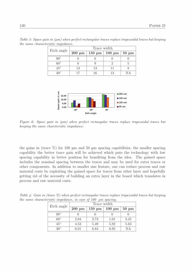
130 Paper D
Table 3: Space gain in (μm) when perfect rectangular traces replace trapezoidal traces but keepingthe same characteristic impedance.
Etch angleTrace width
200 μm 150 μm 100 μm 50 μm
90◦ 0 0 0 0
60◦ 6 9 2 5
45◦ 13 13 11 8
30◦ 17 16 13 NA
0.005.00
10.0015.00
60° 45° 30°Etch angle
Spa
ce g
ain
in u
m 200 um
150 um
100 um
50 um
Figure 6: Space gain in (μm) when perfect rectangular traces replace trapezoidal traces butkeeping the same charcteristic impedance.
the gains in (trace %) for 100 μm and 50 μm spacing capabilities, the smaller spacingcapability the better trace gain will be achieved which puts the technology with lowspacing capability in better position for benefiting from the idea. The gained spaceincludes the nominal spacing between the traces and may be used for extra traces orother components. In addition to smaller size feature, one can reduce process and rawmaterial costs by exploiting the gained space for traces from other layer and hopefullygetting rid of the necessity of building an extra layer in the board which translates inprocess and raw material costs.
Table 4: Gain in (trace %) when perfect rectangular traces replace trapezoidal traces but keepingthe same characteristic impedance, in case of 100 μm spacing.
Etch angleTrace width
200 μm 150 μm 100 μm 50 μm
90◦ 0 0 0 0
60◦ 2.04 3.73 1.01 3.45
45◦ 4.53 5.49 5.82 5.63
30◦ 6.01 6.84 6.95 NA

4. Trading characteristic impedance error for better crosstalk 131
Table 5: Gain in (trace %) when perfect rectangular traces replace trapezoidal traces but keepingthe same characteristic impedance, in case of 50 μm spacing.
Etch angleTrace width
200 μm 150 μm 100 μm 50 μm
90◦ 0 0 0 0
60◦ 2.46 4.71 1.35 5.26
45◦ 5.49 6.95 7.91 8.7
30◦ 7.3 8.7 9.49 NA
4 Trading characteristic impedance error for better
crosstalk
Crosstalk prediction and reduction have always been two essential topics to design forreliable high speed and dense electronics. One of the most popular techniques whichreduces the crosstalk is to use a guard trace between the victim and the aggressor lines,the guard trace which is grounded at two or more points along its length will shieldthe traces it lies between [3], on the other hand the guard trace method does not helpfor low cost and dense electronics. Another interesting technique which is published in[4], suggests to use asymmetric stub loaded lines, the method significantly reduces thenear-end and far-end crosstalk, however implementing stubs between traces for extremelysmall spacing such 100 μm and 50 μm might very hard with the current manufacturingprocess.
According to [5], increasing SW
must lead to near-end and far-end crosstalk reductions,where S is the spacing between the traces and W is the width of the traces. In thissection we will present some simulation results of the crosstalk reduction when applyingthe assumption which is described in section 3. Instead of employing gained space forimproving board density, this time we use the gained space to increase the proximity ofthe traces. Figure 7 shows four cases, where (a) is the original case of the perfect etchingprocess without characteristic impedance error and with S spacing between the traces, (b)is the case where we tolerate the characteristic impedance error of 60◦ trapezoidal tracein perfect rectangular traces and therefore the spacing becomes S + d1 where d1 satisfiesthe condition of keeping the center of the traces at the same X position. This appliessimilarly to case (c) and (d) which correspond to 45◦ and 30◦ trapezoidal microstriplines.
Increasing the spacing S is one way to reduce the mutual coupling, in this case we doincrease the spacing between the traces, but the trace width is also minimized in order tokeep the same board density as 90◦ etch angle. Tables 6 and 7 illustrates the reduction inthe near-end crosstalk S31 for four typical widths and two spacing capabilities. Althoughit is not significant but it might be worthwhile to take into consideration in some appli-cations. According to figure 8 and 9, the crosstalk reduction is almost constant between1 cm and 5 cm length of the coupled lines.

132 Paper D
Figure 7: Basic idea of reducing the crosstalk.
Table 6: Crosstalk reduction in (dB) when perfect rectangular traces replace trapezoidal tracesbut keeping the same characteristic impedance, in case of 100 μm spacing.
Etch angleTrace width
200 μm 150 μm 100 μm 50 μm
90◦ 0 0 0 0
60◦ 0.21 0.55 0.33 0.43
45◦ 0.64 0.78 0.67 0.76
30◦ 0.89 0.95 0.08 NA
Table 7: Crosstalk reduction in (dB) when perfect rectangular traces replace trapezoidal tracesbut keeping the same characteristic impedance, in case of 50 μm spacing.
Etch angleTrace width
200 μm 150 μm 100 μm 50 μm
90◦ 0 0 0 0
60◦ 0.39 0.64 0.21 0.24
45◦ 0.85 0.96 0.94 0.5
30◦ 1.07 1.19 1.11 NA
Figure 8: S31 plot of the four etch cases for 150 μm width, 50 μm spacing and 5 cm trace.

5. Conclusion 133
Figure 9: S31 plot of the four etch cases for 150 μm width, 50 μm spacing and 1 cm trace.
5 Conclusion
This work shows that the etch angle has a significant impact on the characteristicimpedance. Trading the characteristic impedance error for space and raw material whena 90◦ etch angle process is feasible, could be beneficial for high production volumes andcan be a cost saving source if it results in reduced number of layers in HDI boards.Employing similar idea and trading characteristic impedance error for crosstalk reduc-tions lead to a small improvement which can be beneficial in applications where crosstalkreduction has a high priority.
References
[1] S. Monroe and O. Buhler, “The effect of etch factor on printed wiring charactaristicimpedance.” IEEE EMC Society, 2001.
[2] C. F. Coombs, Printed Circuits Handbook, 6th ed. McGraw-Hill Professional Pub-lishing, 2007, ch. 2 - Electronic Packaging and High-Density Interconnectivity, pp.2.16–2.21.

134 Paper D
[3] D. Ladd, “Spice simulation used to characterize the cross-talk reduction effect ofadditional tracks grounded with vias on printed circuit boards,” IEEE Transactionson, 1992.
[4] S.-K. Koo and H.-S. Lee, “Crosstalk reduction effect of asymmetric stub loaded lines,”J. of Electromagn. Waves and Appl, 2011.
[5] Y.-S. Sohn, “Empirical equations on electrical parameters of coupled microstrip linesfor crosstalk estimation in printed circuit board,” IEEE Transactions on, 2oo1.

