digital system design with plds and fpgas -...
TRANSCRIPT
1
11
Digital System Design with PLDs and FPGAs
Kuruvilla Varghese
DESE
Indian Institute of Science
Kuruvilla Varghese
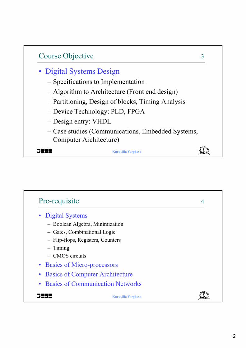
22Your Idea or Expectation
• What is your idea of this course?
• Why are you learning this course?
• What do you think should be taught?
Kuruvilla Varghese
2
33Course Objective
• Digital Systems Design
– Specifications to Implementation
– Algorithm to Architecture (Front end design)
– Partitioning, Design of blocks, Timing Analysis
– Device Technology: PLD, FPGA
– Design entry: VHDL
– Case studies (Communications, Embedded Systems,
Computer Architecture)
Kuruvilla Varghese
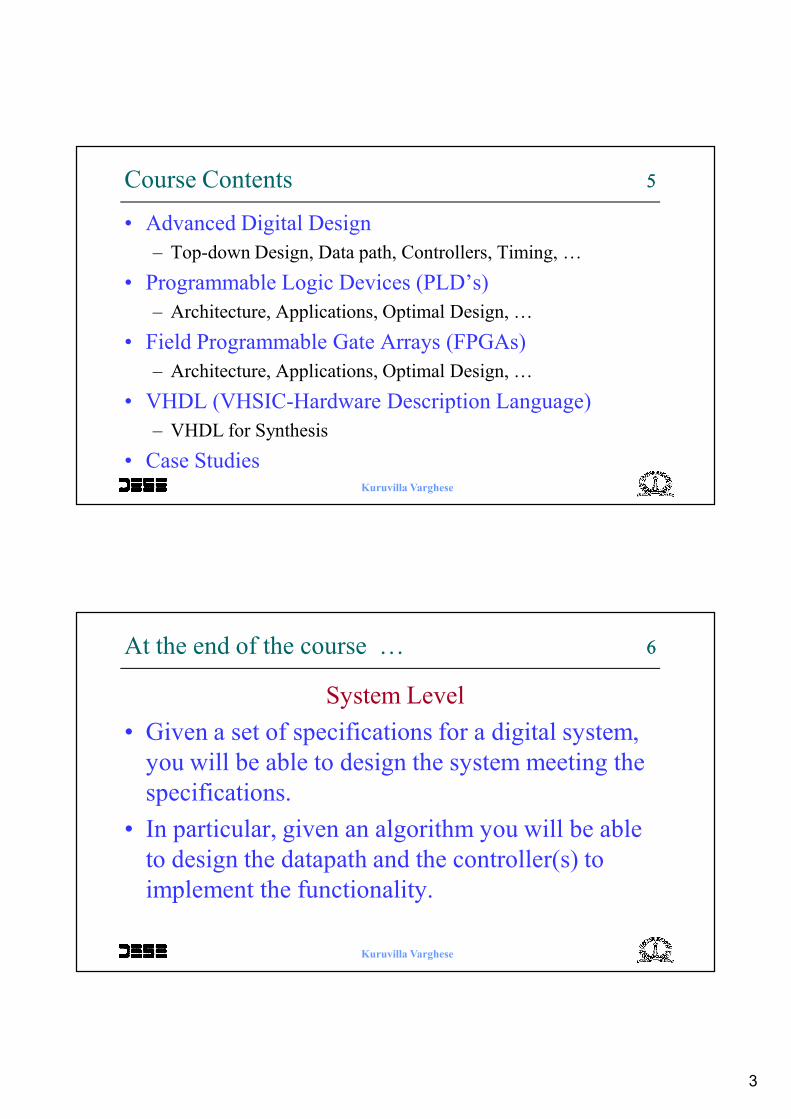
44Pre-requisite
• Digital Systems
– Boolean Algebra, Minimization
– Gates, Combinational Logic
– Flip-flops, Registers, Counters
– Timing
– CMOS circuits
• Basics of Micro-processors
• Basics of Computer Architecture
• Basics of Communication Networks
Kuruvilla Varghese
3
55Course Contents
• Advanced Digital Design
– Top-down Design, Data path, Controllers, Timing, …
• Programmable Logic Devices (PLD’s)
– Architecture, Applications, Optimal Design, …
• Field Programmable Gate Arrays (FPGAs)
– Architecture, Applications, Optimal Design, …
• VHDL (VHSIC-Hardware Description Language)
– VHDL for Synthesis
• Case StudiesKuruvilla Varghese
66At the end of the course …
System Level
• Given a set of specifications for a digital system,
you will be able to design the system meeting the
specifications.
• In particular, given an algorithm you will be able
to design the datapath and the controller(s) to
implement the functionality.
Kuruvilla Varghese
4
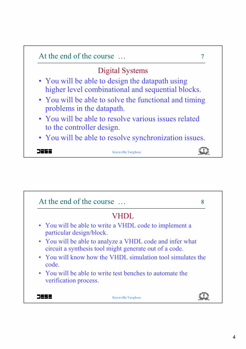
77At the end of the course …
Digital Systems
• You will be able to design the datapath using higher level combinational and sequential blocks.
• You will be able to solve the functional and timing problems in the datapath.
• You will be able to resolve various issues related to the controller design.
• You will be able to resolve synchronization issues.
Kuruvilla Varghese
88At the end of the course …
VHDL
• You will be able to write a VHDL code to implement a particular design/block.
• You will be able to analyze a VHDL code and infer what circuit a synthesis tool might generate out of a code.
• You will know how the VHDL simulation tool simulates the code.
• You will be able to write test benches to automate the verification process.
Kuruvilla Varghese
5
99At the end of the course …
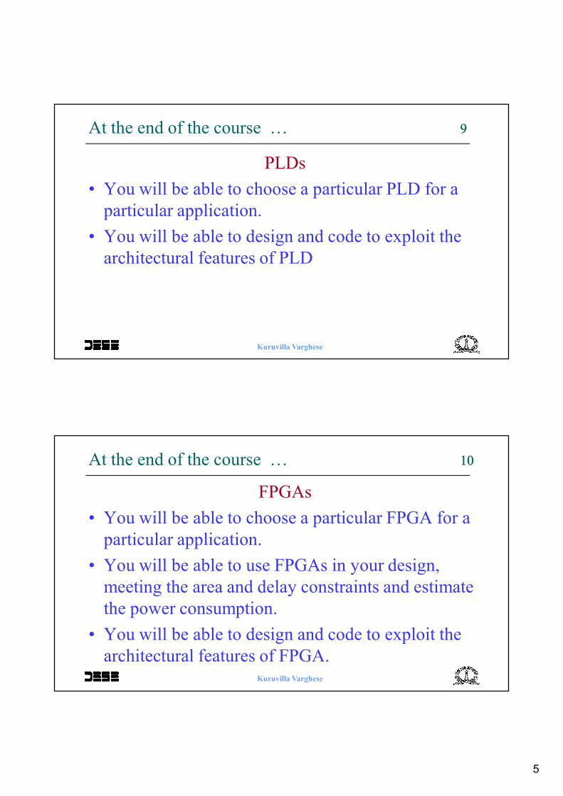
PLDs
• You will be able to choose a particular PLD for a
particular application.
• You will be able to design and code to exploit the
architectural features of PLD
Kuruvilla Varghese
1010At the end of the course …
FPGAs
• You will be able to choose a particular FPGA for a
particular application.
• You will be able to use FPGAs in your design,
meeting the area and delay constraints and estimate
the power consumption.
• You will be able to design and code to exploit the
architectural features of FPGA.Kuruvilla Varghese
6
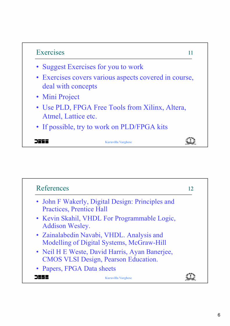
1111Exercises
• Suggest Exercises for you to work
• Exercises covers various aspects covered in course,
deal with concepts
• Mini Project
• Use PLD, FPGA Free Tools from Xilinx, Altera,
Atmel, Lattice etc.
• If possible, try to work on PLD/FPGA kits
Kuruvilla Varghese
1212References
• John F Wakerly, Digital Design: Principles and Practices, Prentice Hall
• Kevin Skahil, VHDL For Programmable Logic, Addison Wesley.
• Zainalabedin Navabi, VHDL. Analysis and Modelling of Digital Systems, McGraw-Hill
• Neil H E Weste, David Harris, Ayan Banerjee, CMOS VLSI Design, Pearson Education.
• Papers, FPGA Data sheets
Kuruvilla Varghese
7
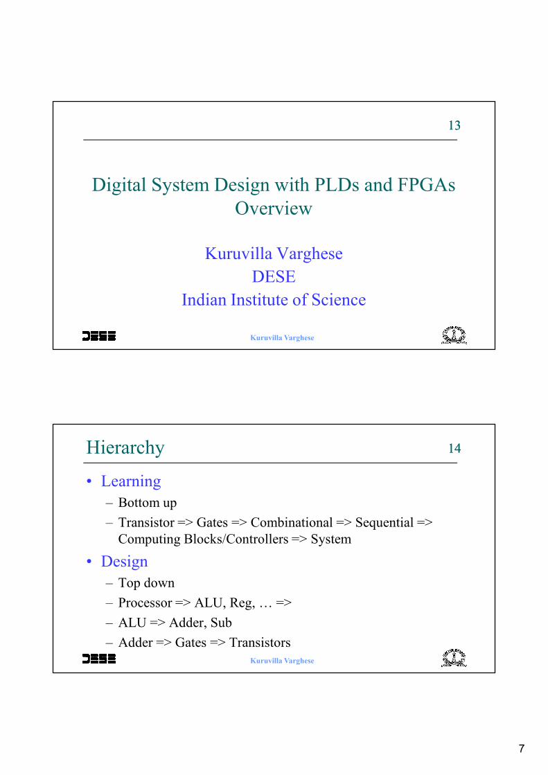
1313
Kuruvilla Varghese
Digital System Design with PLDs and FPGAs
Overview
Kuruvilla Varghese
DESE
Indian Institute of Science
1414Hierarchy
• Learning
– Bottom up
– Transistor => Gates => Combinational => Sequential =>
Computing Blocks/Controllers => System
• Design
– Top down
– Processor => ALU, Reg, … =>
– ALU => Adder, Sub
– Adder => Gates => Transistors
Kuruvilla Varghese
8
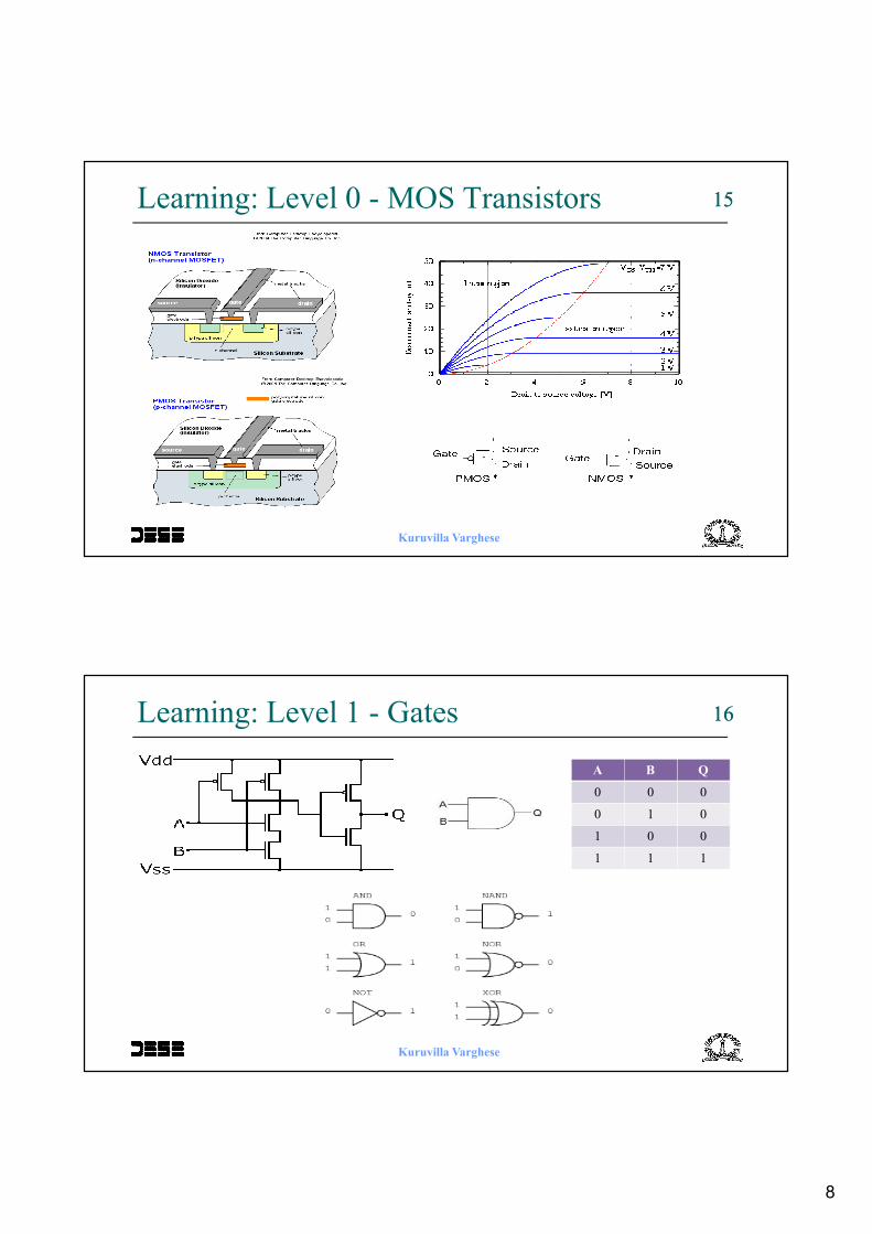
1515Learning: Level 0 - MOS Transistors
Kuruvilla Varghese
1616Learning: Level 1 - Gates
Kuruvilla Varghese
A B Q
0 0 0
0 1 0
1 0 0
1 1 1
9
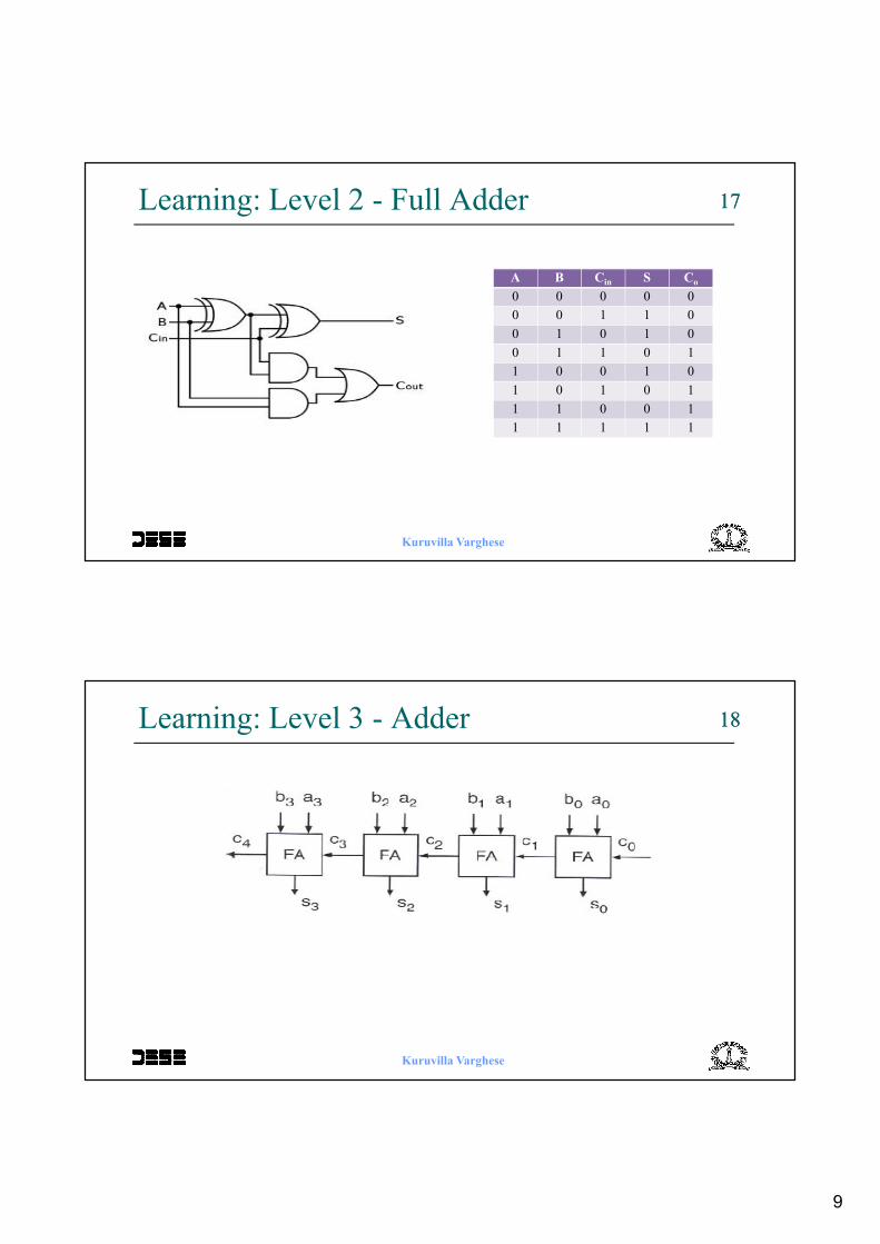
1717Learning: Level 2 - Full Adder
Kuruvilla Varghese
A B Cin S Co
0 0 0 0 0
0 0 1 1 0
0 1 0 1 0
0 1 1 0 1
1 0 0 1 0
1 0 1 0 1
1 1 0 0 1
1 1 1 1 1
1818Learning: Level 3 - Adder
Kuruvilla Varghese
10
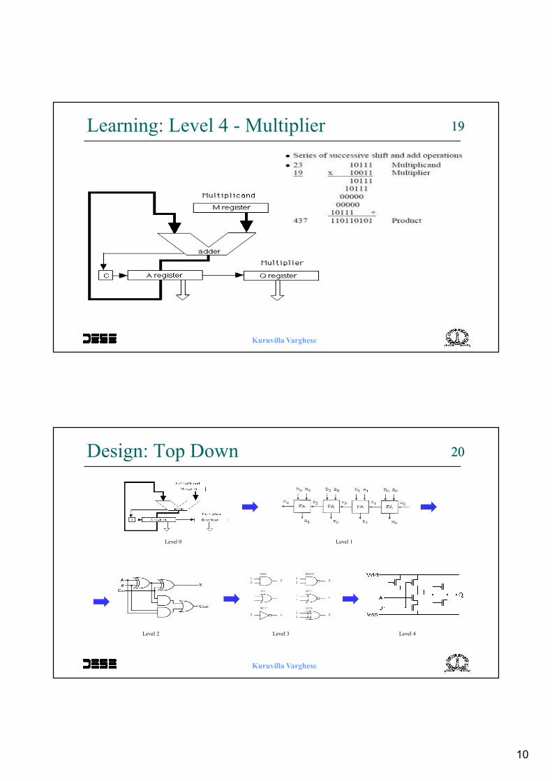
1919Learning: Level 4 - Multiplier
Kuruvilla Varghese
2020Design: Top Down
Kuruvilla Varghese
Level 0 Level 1
Level 2 Level 3 Level 4
11
2121
Kuruvilla Varghese
Digital Design: Major Constituents
• Function / Logic
• Combinational
– Boolean Algebra, Minimization, Functions, Gates,
Encoders, Decoders, Multiplexers, Demultiplexers,
Parity circuits, Comparators, Priority encoders, Open-
drain outputs, and Tri-state outputs, Schmitt-trigger
inputs, Adders, Subtractors, Incrementer, Decrementer,
…
2222
Kuruvilla Varghese
Major Constituents: Functionality / Logic
• Sequential
– Flip-Flops, Latches
– Counters, Registers, Shift Registers
– Finite State Machines (FSM)
– ROM, EPROM, EEPROM
– SRAM, SSRAM
– DRAM, SDRAM
– FIFO
– CAM
12
2323Minimization
• Karnaugh Maps
– Graphical tool, for humas
• Quine-McCluskey (QM)
– Minimal solution, Complexity
• Espresso
– Heuristic based on QM, Faster
– Near minimal solution
Kuruvilla Varghese
2424Minimization
• Multi-Level minimization
– Decomposition (in to multiple terms)
– Extraction of common sub-expressions of multiple
outputs
– Factoring
– Substitution
– Flattening
Kuruvilla Varghese

13
2525Functions and Gates: AND
A B Y
0 0 0
0 1 0
1 0 0
1 1 1
Kuruvilla Varghese
A B Y
0 0 0
0 1 0
1 0 0
1 1 1
A, B and Y Active High
A
BY
A, B and Y Active Low
A
BY
Y = A B
Y/ = A/ + B/ De Morgan’s Theorem
2626Functions and Gates: AND
Kuruvilla Varghese
• AND Gate – AND, and OR Functions
14
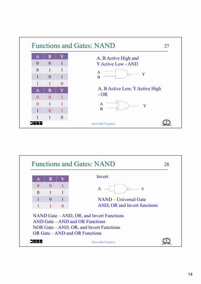
2727Functions and Gates: NAND
A B Y
0 0 1
0 1 1
1 0 1
1 1 0
Kuruvilla Varghese
A B Y
0 0 1
0 1 1
1 0 1
1 1 0
A, B Active High and
Y Active Low - AND
A, B Active Low, Y Active High
- OR
A
BY
A
BY
2828Functions and Gates: NAND
A B Y
0 0 1
0 1 1
1 0 1
1 1 0
Kuruvilla Varghese
Invert
NAND – Universal Gate
AND, OR and Invert functions
A Y
NAND Gate – AND, OR, and Invert Functions
AND Gate – AND and OR Functions
NOR Gate – AND, OR, and Invert Functions
OR Gate – AND and OR Functions
15
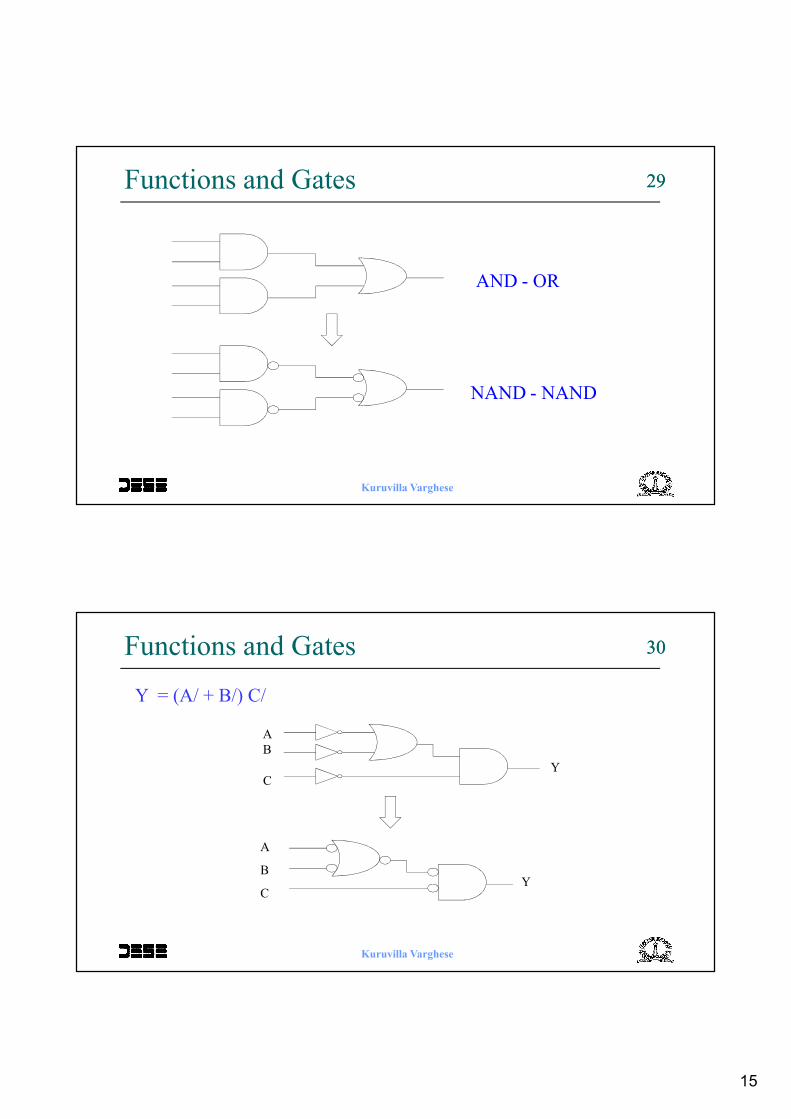
2929Functions and Gates
Kuruvilla Varghese
AND - OR
NAND - NAND
3030Functions and Gates
Kuruvilla Varghese
A
B
Y
Y
A
B
C
Y = (A/ + B/) C/
C
16
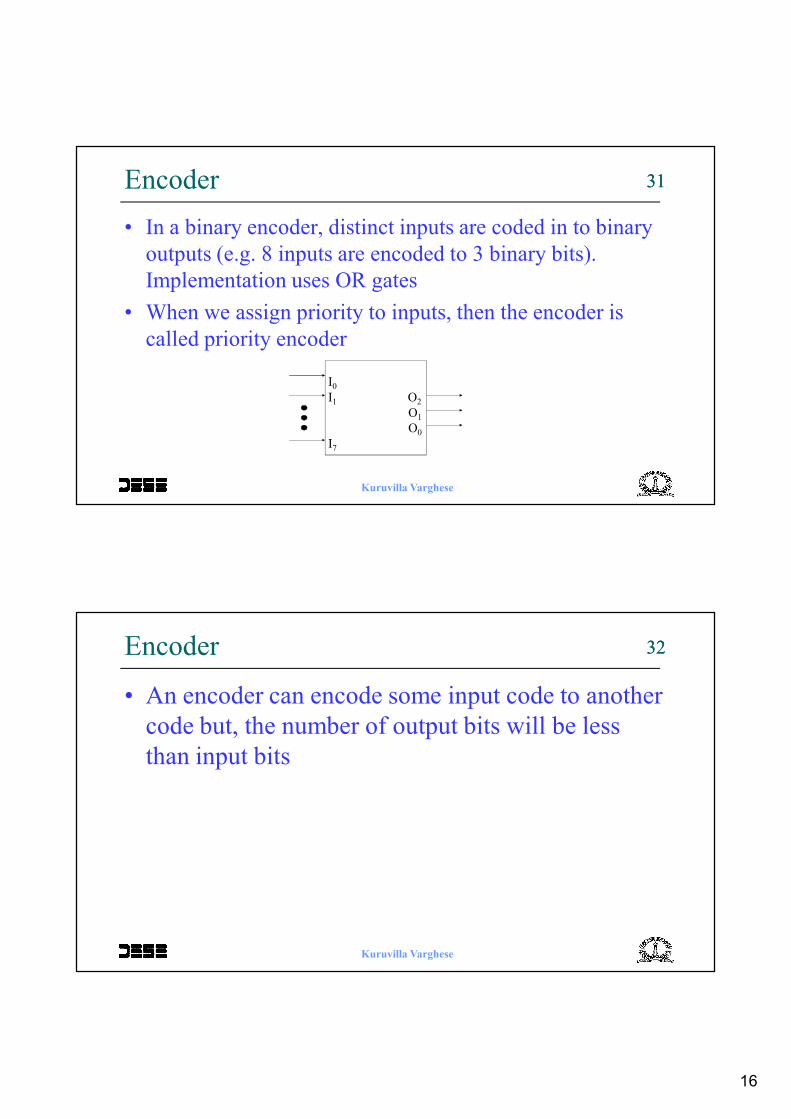
3131Encoder
• In a binary encoder, distinct inputs are coded in to binary
outputs (e.g. 8 inputs are encoded to 3 binary bits).
Implementation uses OR gates
• When we assign priority to inputs, then the encoder is
called priority encoder
Kuruvilla Varghese
I0
I1 O2
O1
O0
I7
3232Encoder
• An encoder can encode some input code to another
code but, the number of output bits will be less
than input bits
Kuruvilla Varghese
17
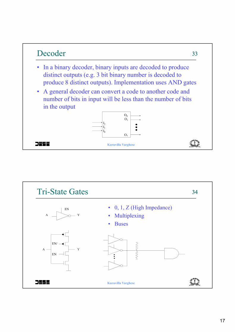
3333Decoder
• In a binary decoder, binary inputs are decoded to produce
distinct outputs (e.g. 3 bit binary number is decoded to
produce 8 distinct outputs). Implementation uses AND gates
• A general decoder can convert a code to another code and
number of bits in input will be less than the number of bits
in the output
Kuruvilla Varghese
O0
O1
I2
I1
I0
O7
3434Tri-State Gates
• 0, 1, Z (High Impedance)
• Multiplexing
• Buses
Kuruvilla Varghese
A Y
EN/
EN
A Y
EN
18
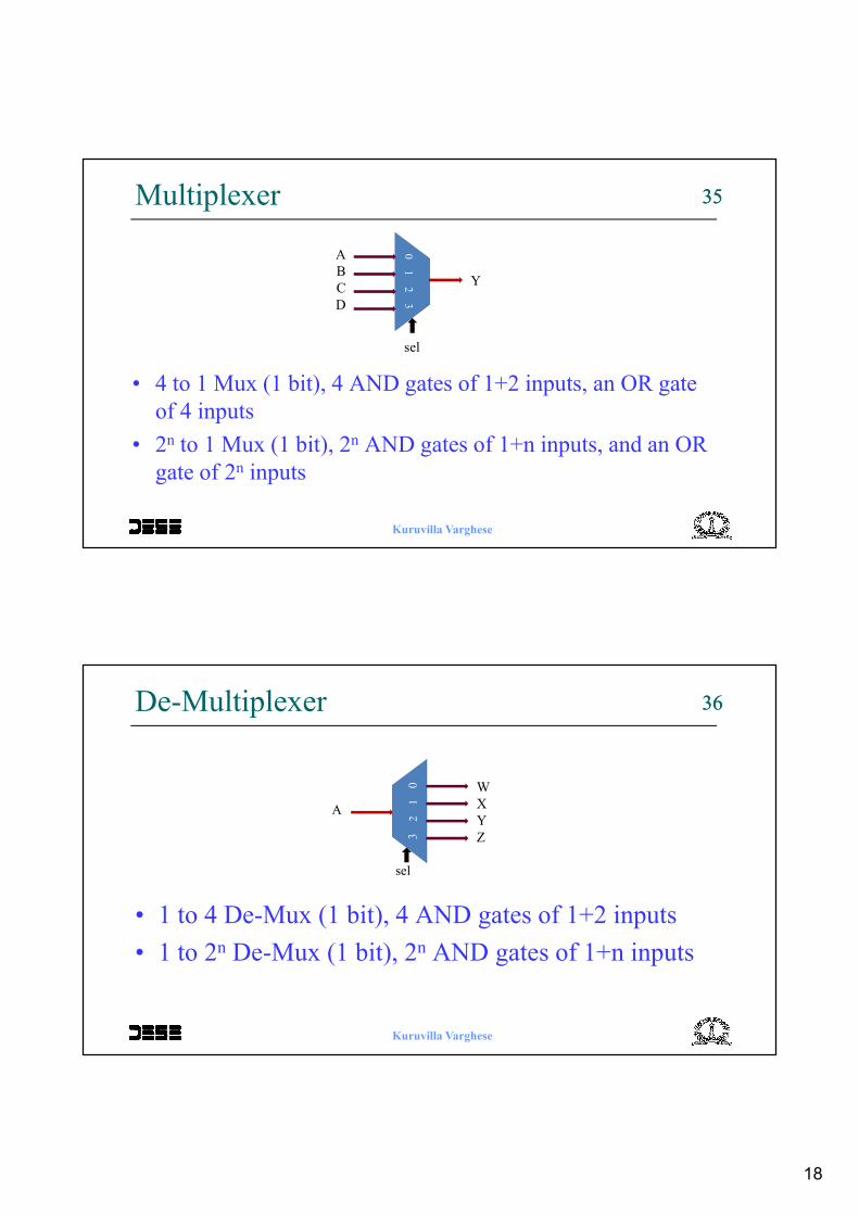
3535Multiplexer
• 4 to 1 Mux (1 bit), 4 AND gates of 1+2 inputs, an OR gate
of 4 inputs
• 2n to 1 Mux (1 bit), 2n AND gates of 1+n inputs, and an OR
gate of 2n inputs
Kuruvilla Varghese
0 1
2 3
A
B
C
D
sel
Y
3636De-Multiplexer
• 1 to 4 De-Mux (1 bit), 4 AND gates of 1+2 inputs
• 1 to 2n De-Mux (1 bit), 2n AND gates of 1+n inputs
Kuruvilla Varghese
3
2
1
0 W
X
Y
Z
sel
A
19
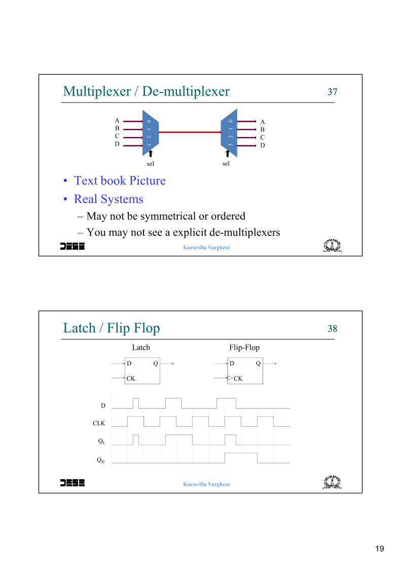
3737Multiplexer / De-multiplexer
• Text book Picture
• Real Systems
– May not be symmetrical or ordered
– You may not see a explicit de-multiplexers
Kuruvilla Varghese
3
2
1
0 A
B
C
D
sel
0 1
2 3
A
B
C
D
sel
3838Latch / Flip Flop
Kuruvilla Varghese
D
CLK
QL
QD
D Q
CK
D Q
CK
Latch Flip-Flop
20
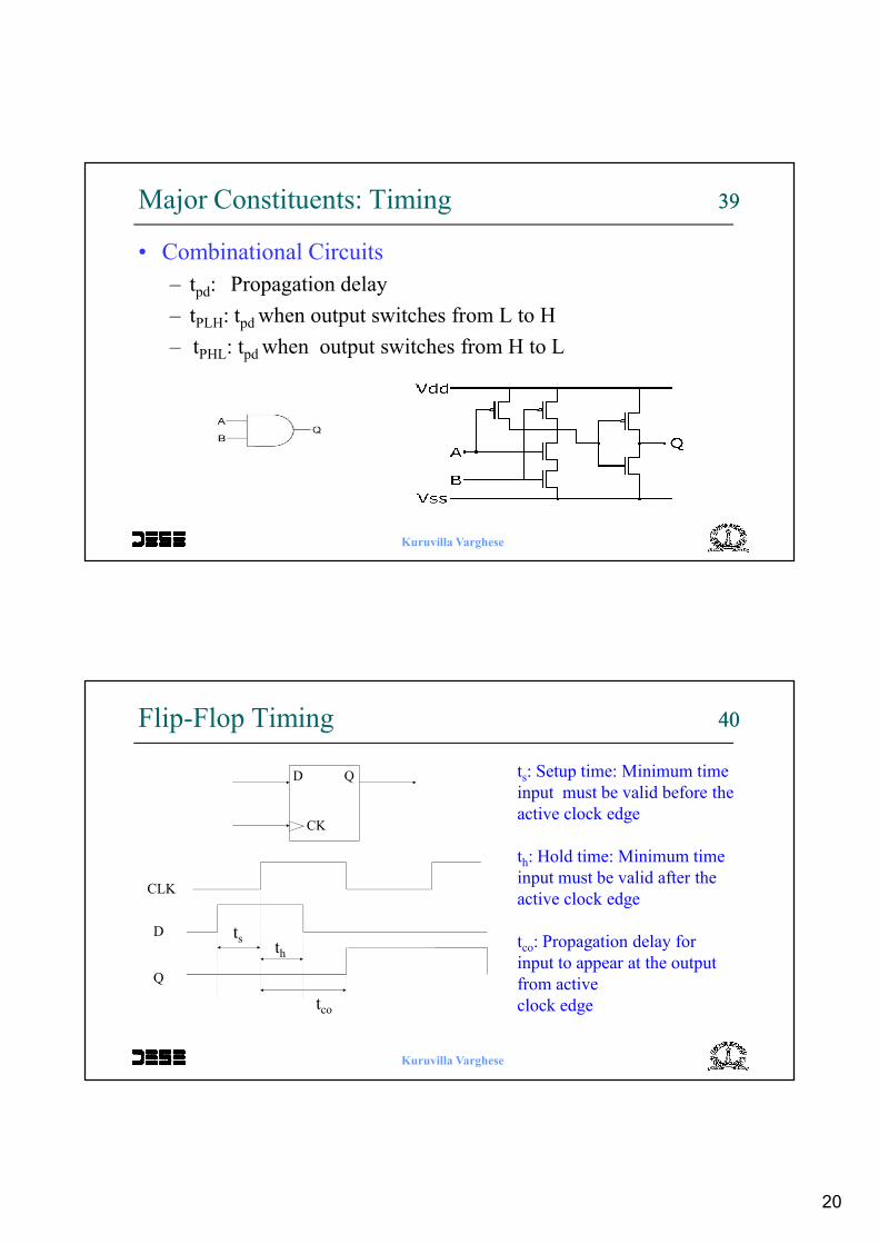
3939
Kuruvilla Varghese
Major Constituents: Timing
• Combinational Circuits
– tpd: Propagation delay
– tPLH: tpd when output switches from L to H
– tPHL: tpd when output switches from H to L
4040Flip-Flop Timing
Kuruvilla Varghese
D Q
CK
CLK
D
Q
tsth
tco
ts: Setup time: Minimum time
input must be valid before the
active clock edge
th: Hold time: Minimum time
input must be valid after the
active clock edge
tco: Propagation delay for
input to appear at the output
from active
clock edge
21
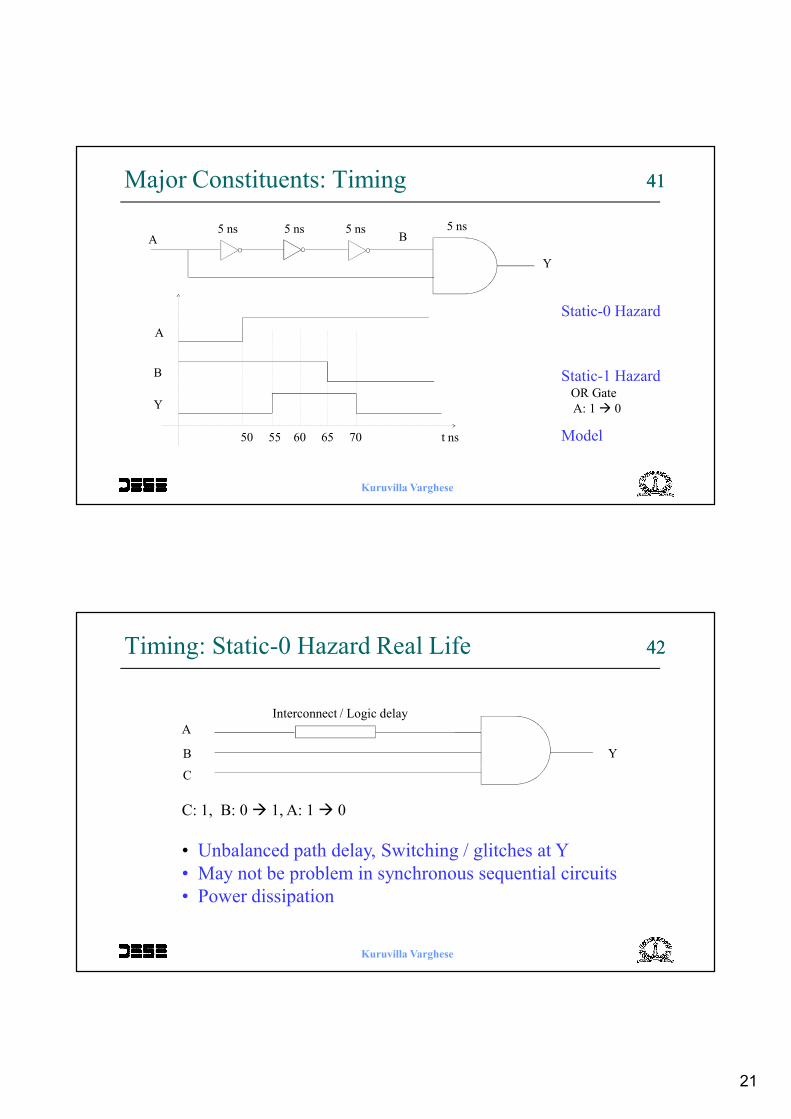
4141
Kuruvilla Varghese
Major Constituents: Timing
t ns50 55 60 65 70
A
B
Y
Static-0 Hazard
Static-1 HazardOR Gate
A: 1 � 0
Model
A B
Y
5 ns 5 ns 5 ns 5 ns
4242
Kuruvilla Varghese
Timing: Static-0 Hazard Real Life
Y
A
B
C
Interconnect / Logic delay
C: 1, B: 0 � 1, A: 1 � 0
• Unbalanced path delay, Switching / glitches at Y
• May not be problem in synchronous sequential circuits
• Power dissipation
22
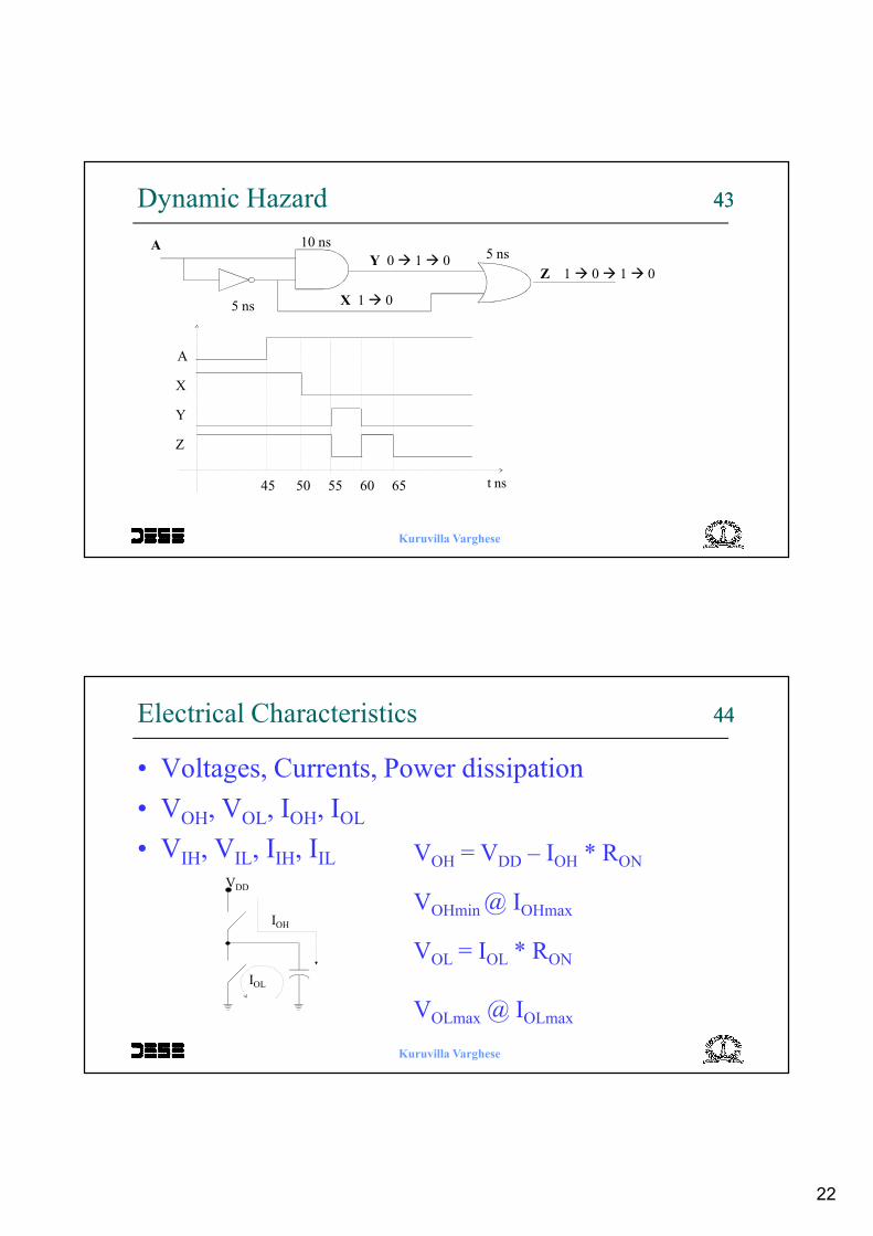
4343
Kuruvilla Varghese
Dynamic Hazard
10 nsA
X 1 � 0
Y 0 � 1 � 0Z 1 � 0 � 1 � 0
5 ns
5 ns
t ns45 50 55 60 65
A
X
Y
Z
4444
Kuruvilla Varghese
Electrical Characteristics
• Voltages, Currents, Power dissipation
• VOH, VOL, IOH, IOL
• VIH, VIL, IIH, IIL VOH = VDD – IOH * RON
VOHmin @ IOHmax
VOL = IOL * RON
VOLmax @ IOLmax
IOH
IOL
VDD
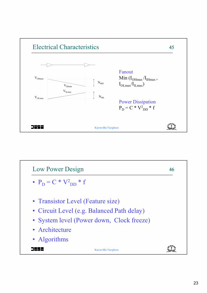
23
4545
Kuruvilla Varghese
Electrical Characteristics
VOHmin
VOLmax
VIHmin
VILmax
NMH
NML
Fanout
Min (IOHmax /IIHmax ,
IOLmax/IILmax)
Power Dissipation
PD = C * V2DD * f
4646
Kuruvilla Varghese
Low Power Design
• PD = C * V2DD * f
• Transistor Level (Feature size)
• Circuit Level (e.g. Balanced Path delay)
• System level (Power down, Clock freeze)
• Architecture
• Algorithms
24
4747
Kuruvilla Varghese
High Frequency Designs
• Transmission Lines
• Reflections
• Cross talk
• Ground loops
• Back end Tools
4848
Kuruvilla Varghese
Device Technology
• Full Custom (ASIC)
– High NRE Cost, High Volume
– Large Turn around time
– Custom design from scratch
– Use of library cells
• Semi Custom (Mask Programmable / Standard Cell)
– Design in terms of standard blocks
– Medium NRE Cost, Medium Volume
– Medium Turn around time
25
4949
Kuruvilla Varghese
Device Technology
• Field Programmable (FPGA)
– Low NRE Cost, Low-Medium Volume
– Low Turn around time
5050VLSI Technology
• PMOS is getting faster (hole mobility)
• Strained silicon
• Current Feature Size 22 nm (Intel Core i3, i5, i7)
• Future Feature Size 14 nm
• Inverter Delay 5-7 ps
Kuruvilla Varghese
26
5151
Kuruvilla Varghese
Design Methodology
• Front-end design
– Specifications => Gate and Flip-flop Net list
– Algorithm => Architecture => Circuit
• Back-end design
– Gate and Flip-flop Net list => Chip Masks
– Circuit => Transistor Level Circuit => Chip masks
– Circuit => Configuration pattern (FPGA)
5252
Kuruvilla Varghese
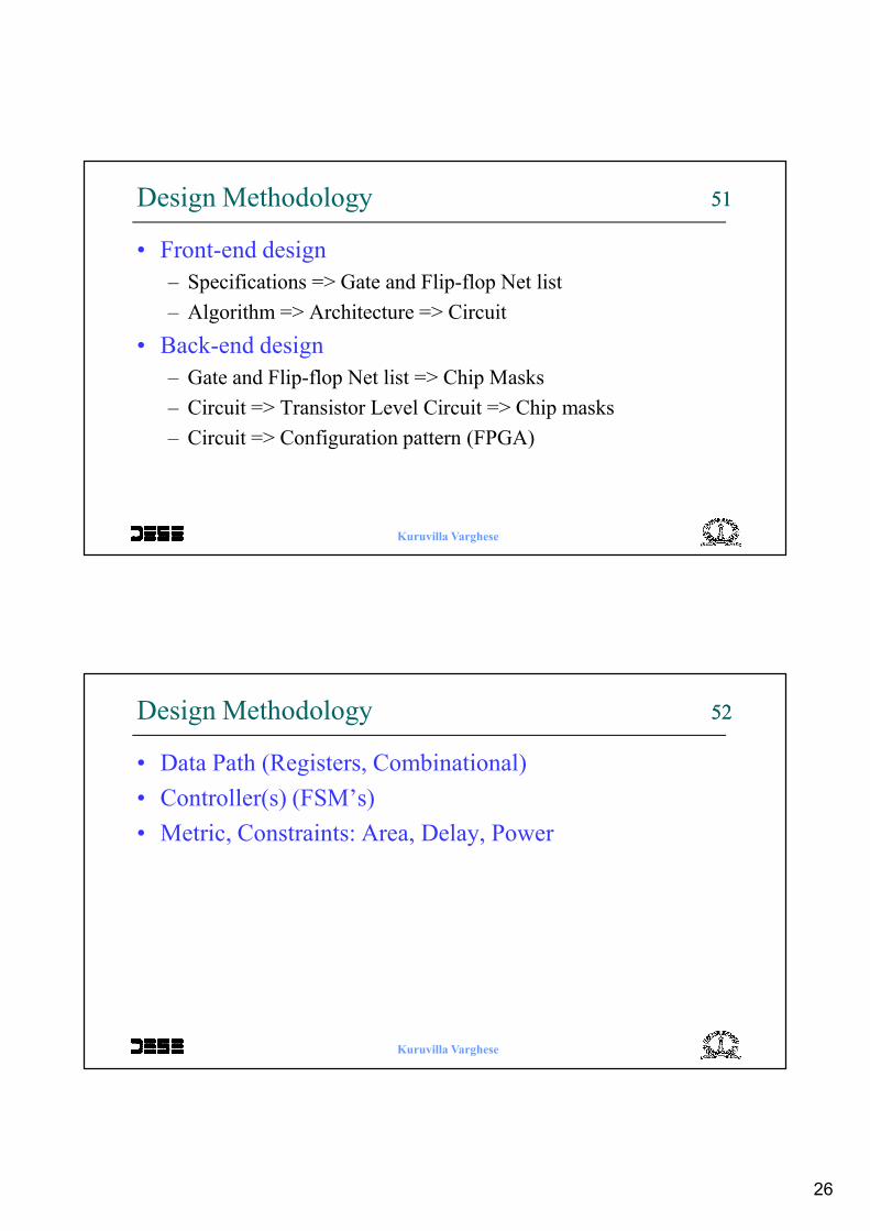
Design Methodology
• Data Path (Registers, Combinational)
• Controller(s) (FSM’s)
• Metric, Constraints: Area, Delay, Power
27
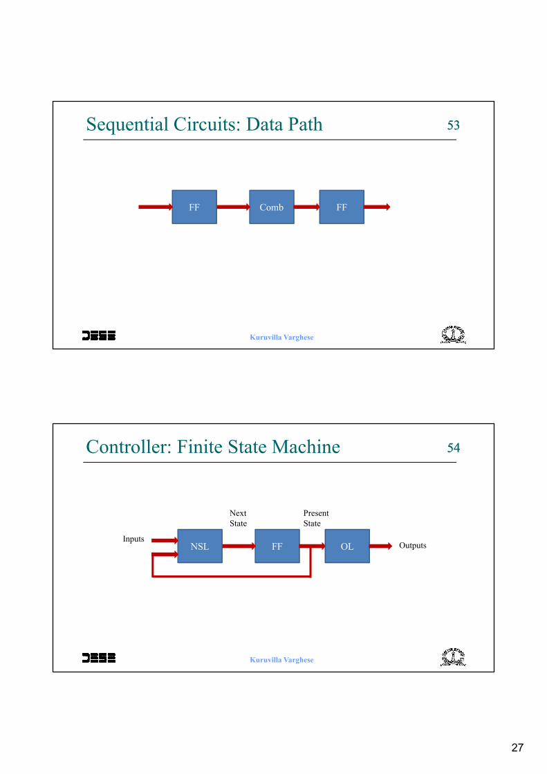
5353Sequential Circuits: Data Path
Kuruvilla Varghese
CombFF FF
5454Controller: Finite State Machine
Kuruvilla Varghese
FFNSL OLInputs
Outputs
Present
State
Next
State
28
5555
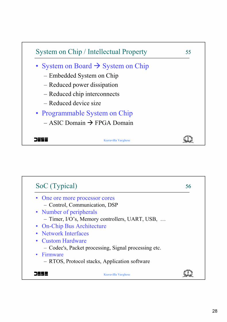
Kuruvilla Varghese
System on Chip / Intellectual Property
• System on Board � System on Chip
– Embedded System on Chip
– Reduced power dissipation
– Reduced chip interconnects
– Reduced device size
• Programmable System on Chip
– ASIC Domain � FPGA Domain
5656
Kuruvilla Varghese
SoC (Typical)
• One ore more processor cores– Control, Communication, DSP
• Number of peripherals– Timer, I/O’s, Memory controllers, UART, USB, …
• On-Chip Bus Architecture
• Network Interfaces
• Custom Hardware– Codec's, Packet processing, Signal processing etc.
• Firmware
– RTOS, Protocol stacks, Application software
29
5757
Kuruvilla Varghese
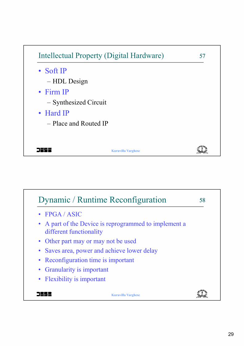
Intellectual Property (Digital Hardware)
• Soft IP
– HDL Design
• Firm IP
– Synthesized Circuit
• Hard IP
– Place and Routed IP
5858Dynamic / Runtime Reconfiguration
• FPGA / ASIC
• A part of the Device is reprogrammed to implement a
different functionality
• Other part may or may not be used
• Saves area, power and achieve lower delay
• Reconfiguration time is important
• Granularity is important
• Flexibility is important
Kuruvilla Varghese
30
5959
Kuruvilla Varghese
System Modeling
• Architecture Exploration, Performance Modeling, High
level Synthesis
• Hardware-Software partitioning
– Cost-performance trade-offs
• Hardware: Concurrent, Higher performance, Higher cost
• Software: Sequential, Lower performance, More flexible
• SystemC
• SystemVerilog: Verification
6060
Kuruvilla Varghese
Application Areas
• Communication Networks
– Physical layer (Mixed-mode design)
– Data link layer (Digital, Mostly in hardware, control in OS
Drivers)
– Network layer (Processing in Hardware for Network elements
like Switches and Routers)
• Signal Processing
– Filters, Codecs, Compression, etc.
• Computer Architecture