diamond microchannel heat sink designs for high heat · pdf filediamond microchannel heat sink...
TRANSCRIPT
AIAA Diamond Microchannel Heat Sink Designs For High Heat Flux Thermal Control
Mr. Michael V. Corbin Mr. Matthew M. DeBenedictis Mr. David B. James Mr. Stephen P. LeBlanc Mr. Leo R. Paradis Raytheon Electronic Systems Tewksbury, MA 01876
11th Annual AIAA/MDA Technology Conference29 July-2 August 2002
Monterey, CA WARNING - This document contains unclassified technical data whose export is restricted by the Arms Export Control Act (Title 22 USC Sec 2751 et seq.) or the Export Administration Act of 1979 (Title 50 USC App 2401 et seq.), as amended. The implementing regulations for these statutes are the International Traffic In Arms Regulations (22 CFR Part 120 et seq.) and the Export Administration Regulations (15 CFR Part 730 et seq.). Dissemination to non-US persons and entities requires an export license or other authorization. Violations of these export laws and regulations are subject to severe criminal, civil and administrative penalties. Approved for Public Release; Distribution is Unlimited.
Report Documentation Page
Report Date 29JUL2002
Report Type N/A
Dates Covered (from... to) -
Title and Subtitle Diamond Microchannel Heat Sink Designs For High HeatFlux Thermal Control
Contract Number
Grant Number
Program Element Number
Author(s) Project Number
Task Number
Work Unit Number
Performing Organization Name(s) and Address(es) Raytheon Electronic Systems Tewksbury, MA 01876
Performing Organization Report Number
Sponsoring/Monitoring Agency Name(s) and Address(es)
Sponsor/Monitor’s Acronym(s)
Sponsor/Monitor’s Report Number(s)
Distribution/Availability Statement Approved for public release, distribution unlimited
Supplementary Notes See Also ADM201460. Papers from Unclassified Proceedings from the 11th Annual AAIA/MDATechnology Conference held in Monterey, CA from 29 Jul - 2 Aug 2002., The original document containscolor images.
Abstract
Subject Terms
Report Classification unclassified
Classification of this page unclassified
Classification of Abstract unclassified
Limitation of Abstract SAR
Number of Pages 12
UNCLASSIFIED
Diamond Microchannel Heat Sink Designs For High Heat Flux Thermal Control
Mr. Michael V. Corbin* Mr. Matthew M. DeBenedictis†
Mr. David B. James‡ Mr. Stephen P. LeBlanc§
Mr. Leo R. Paradis**
Raytheon Electronic Systems Tewksbury, MA 01876
ABSTRACT
Directed energy weapons, wide band gap semiconduc-tor based radars, and other powerful systems present significant thermal control challenges to component designers. Heat Flux levels approaching 2000 W/cm2
are encountered at the base of laser diodes, and levels as high as 500 W/cm2 are expected in laser slabs and power amplifier tube collectors. These impressive heat flux levels frequently combine with strict operating temperature requirements to further compound the thermal control problem. Many investigators have sug-gested the use of diamond heat spreaders to reduce flux levels at or near to its source, and some have suggested that diamond microchannel heat sinks ultimately may play a significant role in the solution of these problems. Design engineers at Raytheon Company have investi-gated the application of all-diamond microchannel heat sinks to representative high heat flux problems and have found the approach promising. Diamond micro-channel fabrication feasibility has been demonstrated; integration into packaging systems and the accompany-ing material compatibility issues have been addressed; and thermal and hydrodynamic performance predictions have been made for selected, possible applications. An example of a practical, all diamond microchannel heat sink has been fabricated, and another is in process and will be performance tested. The heat sink assembly is made entirely of optical quality, CVD diamond and is of sufficient strength to withstand the thermal and pressure-induced mechanical loads associated with
manufacture and use in a tactical weapons environment. The work presented describes the development program’s accomplishments to date, and highlights many of the areas for future study.
I. INTRODUCTION
Development of advanced systems such as Directed Energy Weapons (DEW) and radar using Wide Bandgap Semiconductors (WBS) has highlighted the necessity for innovation in thermal management in the high heat flux regime, (up to 1 kW/cm2) and into the ultra-high (up to 100 kW/cm2) regime1. Recent development activities2,3,4 require heat removal from diode arrays and electromagnetic weapons, reaching the level of 1700 W/sq. cm over small areas typical of thermal diodes, and 500 W/sq. cm over large areas in tube collector regions.
Tuckerman, in his notable 1984 work5, foresaw that thermal control problems of this magnitude would require special solutions and, using classical heat transfer and compact heat exchanger theory, predicted that those solutions would be found in ‘microscopic ducts’. He defined these as having a hydraulic diameter of approximately 50 �m. He went on to fabricate examples of these ‘microchannels’ in silicon, and successfully operated heat sinks with heat input of 1309 W/cm2. In the 1990’s, silicon microchannels were successfully applied to laser diode thermal control at Lawrence Livermore Laboratory, and are still in use for that purpose. In that same era, diamond was being adopted for use as a heat spreader for electronic devices at NASA Goddard6 for space-borne power amplifiers, and for GaAs IMPATT diodes at Raytheon.
More recently, investigators have determined that microchannels in diamond offer the potential to substantially reduce the excellent low thermal resis-tance values realized from silicon microchannel heat sinks, as well as those fabricated from other materials. Goodsen et.al.7 concluded that the thermal resistance offered by silicon could be reduced by 75% if the microchannel was fabricated from diamond with a thermal conductivity of 2000 W/m-K.
* Senior Engineer I, Raytheon Electronic Systems,
Tewksbury, MA, †Senior Engineer II, Raytheon Electronic Systems,
Tewksbury, MA, Raytheon Electronic Systems is a leading manufacturer of Optical Quality Diamond (OQD), using the Micro-wave Assisted Chemical Vapor Deposition (MA/CVD) approach, and has been in the forefront of developing diamond for electromagnetic and infrared widows as well as heat spreaders. The material is deposited at a
‡Principal Engineer I, Raytheon Electronic Systems, Tewksbury, MA, Senior Member, AIAA
§Principal Engineer I, Raytheon Electronic Systems, Tewksbury, MA,
**Engineering Fellow, Raytheon Electronic Systems, Tewksbury, MA, Senior Member AIAA
Approved for Public Release; Distribution is Unlimited.
1 UNCLASSIFIED
UNCLASSIFIED
Optical Quality Diamond
Thermal ManagementGrade Diamond
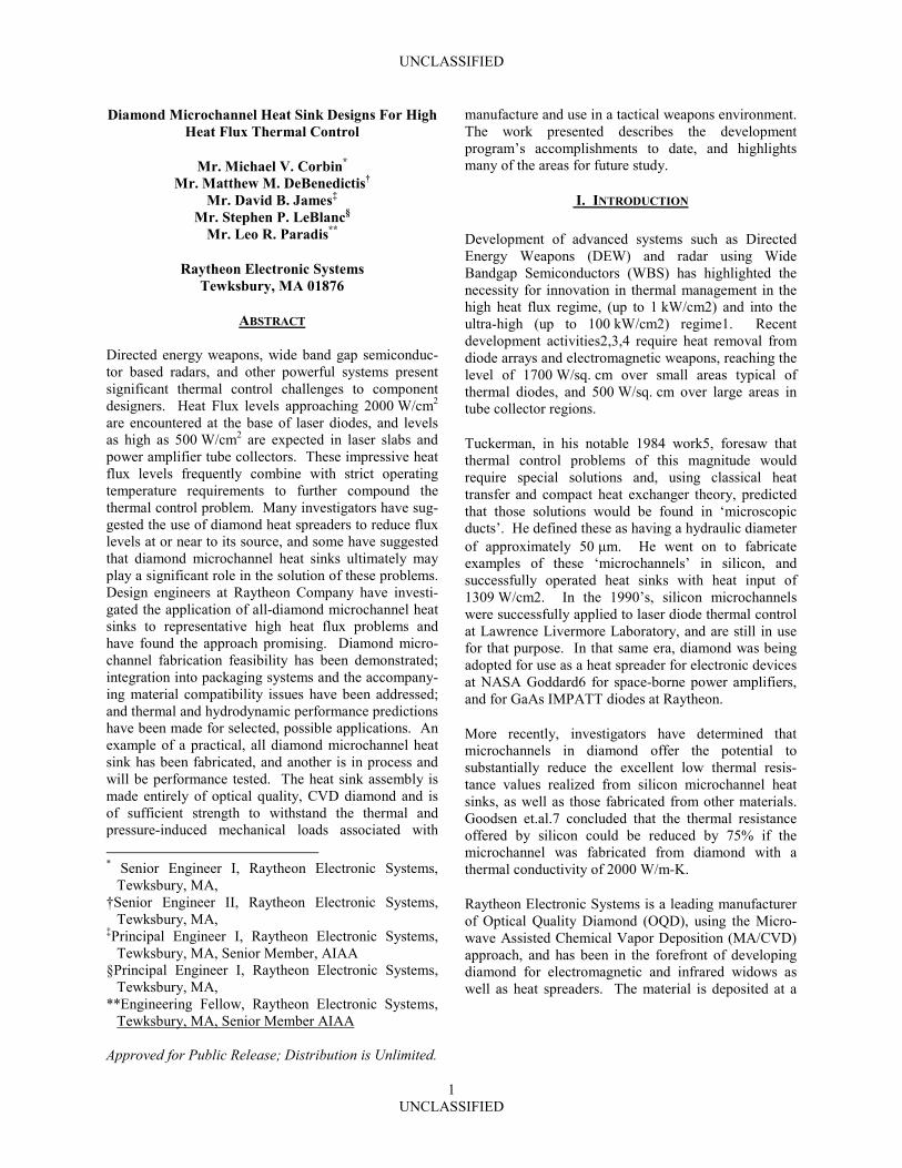
Figure 1. Comparison of Thermal Conductivity of Various Diamond Thermal Control Materials
relatively slow rate in reactors to form small crystals that are optically desirable in window applications. A fortunate byproduct of this is that the OQD has very high thermal conductivity and working strength. Thermal conductivity data for OQD and other materials was acquired in an international diamond property round-robin8, and is shown in Figure 1.
With the recent beginning of development of WBS power amplifiers for radars, application of diamond as a heat spreader was envisioned as a thermal control
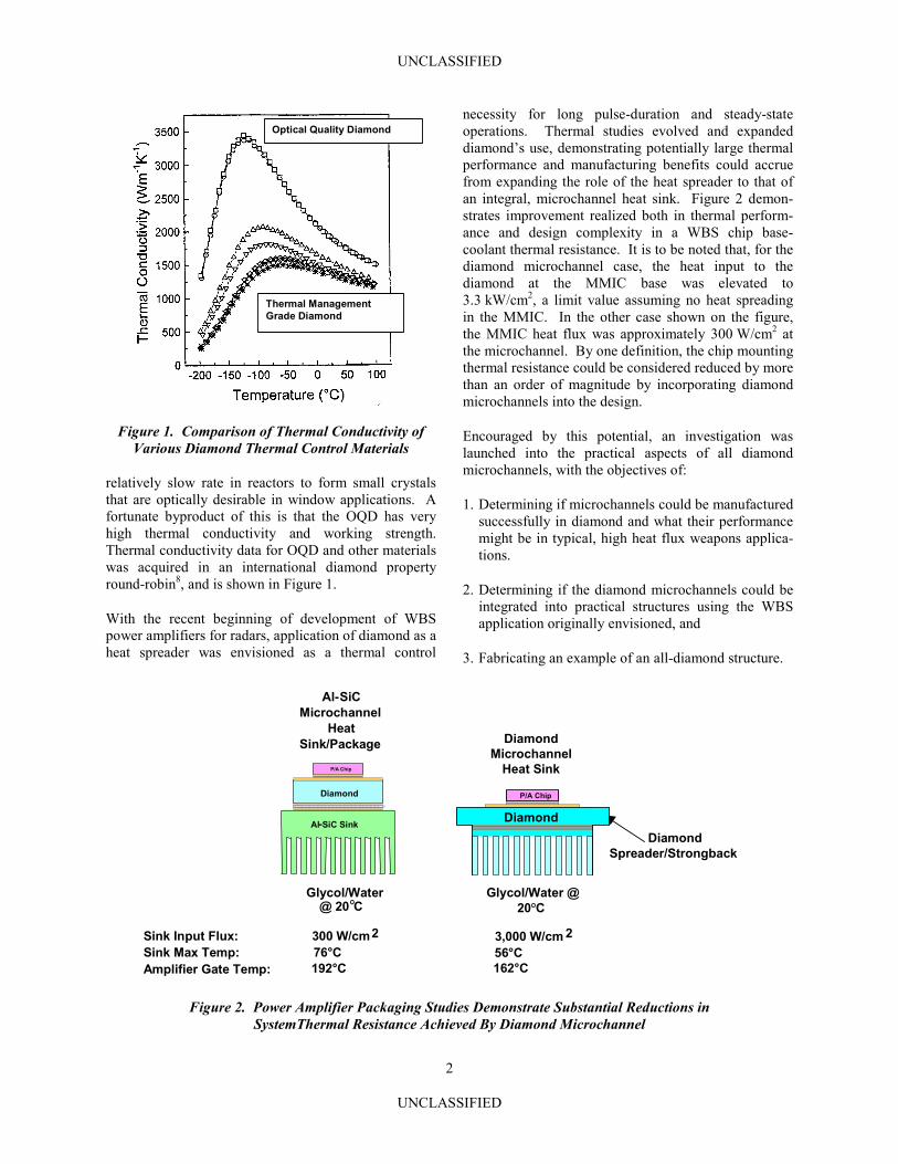
necessity for long pulse-duration and steady-state operations. Thermal studies evolved and expanded diamond’s use, demonstrating potentially large thermal performance and manufacturing benefits could accrue from expanding the role of the heat spreader to that of an integral, microchannel heat sink. Figure 2 demon-strates improvement realized both in thermal perform-ance and design complexity in a WBS chip base-coolant thermal resistance. It is to be noted that, for the diamond microchannel case, the heat input to the diamond at the MMIC base was elevated to 3.3 kW/cm2, a limit value assuming no heat spreading in the MMIC. In the other case shown on the figure, the MMIC heat flux was approximately 300 W/cm2 at the microchannel. By one definition, the chip mounting thermal resistance could be considered reduced by more than an order of magnitude by incorporating diamond microchannels into the design.
Encouraged by this potential, an investigation was launched into the practical aspects of all diamond microchannels, with the objectives of:
1. Determining if microchannels could be manufactured successfully in diamond and what their performance might be in typical, high heat flux weapons applica-tions.
2. Determining if the diamond microchannels could be integrated into practical structures using the WBS application originally envisioned, and
3. Fabricating an example of an all-diamond structure.
Sink Input Flux:Sink Max Temp:Amplifier Gate Temp:
DiamondMicrochannel
Heat Sink
Glycol/Water @20ºC
P/A Chip
DiamondSpreader/Strongback
Al-SiCMicrochannel
HeatSink/Package
Glycol/Water@ 20ºC
Al-SiC Sink
Diamond
P/A Chip
Diamond
3,000 W/cm 2 56°C
162°C
300 W/cm276°C192°C
Figure 2. Power Amplifier Packaging Studies Demonstrate Substantial Reductions in SystemThermal Resistance Achieved By Diamond Microchannel
2
UNCLASSIFIED

UNCLASSIFIED
3
UNCLASSIFIED
Diamond, although possessing remarkable thermal and mechanical properties, can be cut readily by commer-cially available Nd:YAG lasers. This has been done to manufacture extremely fine parts and even to polish the outer surface of hemispherical domes. Beam position control to within a few microns is more than sufficient to cut microchannels. With the theoretical potential for laser-cut microchannels established, a diamond microchannel-cutting experiment was conducted.
A scrap piece of approximately 1 mm thick material was selected for the experiment. The fin geometry programmed was that for 150 �m thick fins on a 300 �m pitch, the dimensions being the same as those of the AlSiC fins shown in Figure 2. Figure 3 shows one of the first attempts, with fins cut to approximately 500 �m in the diamond. This indicated that the fin cutting could proceed nicely to that depth. The laser formed a remarkably smooth wall channel with an irregular root region, possibly reflecting crystal features. There was some channel tapering from the fin tip to the root, which is a desirable feature, in that diamond conductance at the tip need not be as great as at the base. Figure 4 shows an extreme cut to near the full, 1 mm material thickness, aimed at determining if the laser might burn through at such depths. That experiment proved that depth of the fin can be extended to nearly the material thickness, without burning through, although there were some near misses. Clearly, the experiment was a success, proving that microchannel fins could be manufactured in diamond blanks, and some interesting conclusions were drawn:
1. The fin profile would probably be curved, with the radius of curvature tending to decrease with the depth of the fin. It was felt that cutting process improve-ments could largely eliminate this tendency and the filleting exhibited in the shallow cut of Figure 2 ultimately could be approximated in deeper cuts.
2. The controllability of the process, and the smoothness of the vertical walls of the fin, indicated that the diamond fins could be cut very close together, allow-ing literally razor edge at the fin tips, which is an ideal shape considering the high diamond thermal conduc-tivity. This allows more fins/unit width of heat sink, and enlarges the compact heat exchanger face area/flow area/fluid and pressure drop design space.
3. The roughness in the channel base region and the near-miss burn-throughs raised awareness that dia-mond microchannels might be susceptible to struc-tural failure at fin roots. This led to the development of the strongback approach discussed later. Further, it was decided that channel depths of 75% of blank
thickness would be used for performance studies, until further information is available. This, in con-cert with the strongback, serves to retain the ‘heat-spreader’ nature of the diamond, which could be restricted if channels are cut too deep. A positive feature of the fin base region shape was the thought that the surface roughening would enhance heat transfer at that location, and might prove even more valuable if phase change cooling is utilized.
Figure 3. Shallow Depth Diamond Cutting Experiment
The channel shapes generated by the cutting experi-ments led to a brief study aimed at determining, very approximately, the degree to which the fin root should be shaped. A series of approximations of the shapes, as shown in Figure 4 were used, extending from a triangle to a pyramid-base to a rectangle, considered the base line. The shapes studied and the temperature contours developed are shown in Figure 5. Three shapes were modeled and analyzed using Flotherm, a commercial CFD code9. Study results plainly show that the ‘slightly rounded’ channel base is clearly superior to a deep V shape, and is practically equivalent to the rectangular shape in both performance and pressure drop. A further study reduced the fin material thickness to reduce pressure drop, which also increased thermal performance due to eliminating flow stagnating regions along the channel base.

UNCLASSIFIED
0.8
150 UM um
mm
Figure 4. Deep, Burn-through Diamond Cutting Experiment
II. DIAMOND MICROCHANNEL PERFORMANCE PREDICTIONS
A concurrent thermal/fluid dynamics investigation was made to assess the performance of diamond microchan-nel heat sinks when faced with thermal control problems typical of Directed Energy Weapons. DEW present many thermal control challenges due to the very high heat flux levels sustained over significant areas as typified by laser slab cooling, for example, and the significantly higher heat fluxes typical of laser diode arrays. The investigation attempted to determine if there were significant performance improvements to be had by using diamond as key thermal control material with emphasis on the use of coolants that would be found in a tactical weapons environment. Foremost of these is ethylene glycol/water. Polyalphaolefin (PAO) was also studied, but its viscosity limitations seem contradictory to the use of microchannels. Water was used as a reference coolant, as it is widely used in laboratories.
A thermal model of a nominal, all diamond heat sink design was selected for the investigation, shown pictorially in Figure 6. The analytical tool used in the
12.5W0.000641cfmdP=14.8psiRectangular
12.5W0.000641cfmdP=43.0psiDeep Vee
12.5W0.000641cfmdP=17.9psiRounded
Figure 5. Channel Shape/Performance Study Models and Thermal Results
4
UNCLASSIFIED
UNCLASSIFIED
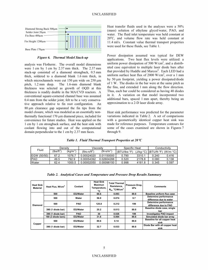
Diamond Strong Back 500�mSolder Joint 20�mFin Base 400�m
Fin Height 1200�m
Base Plate 170�m
Figure 6. Thermal Model Stack-up
analysis was Flotherm.. The overall model dimensions were 1 cm by 1 cm by 2.37 mm thick. The 2.37 mm stack-up consisted of a diamond strongback, 0.5 mm thick, soldered to a diamond blank 1.6 mm thick, in which microchannels were cut 150 �m wide on 250 �m pitch, 1.2 mm deep. The 1.6-mm diamond blank thickness was selected as growth of OQD at this thickness is readily doable in the MA/CVD reactors. A conventional square-cornered channel base was assumed 0.4 mm from the solder joint; felt to be a very conserva-tive approach relative to fin root configuration. An 80 �m clearance gap separated the fin tips from the model closure, which was modeled as an essentially non-thermally functional 170 �m diamond piece, included for convenience for future studies. Heat was applied on the 1 cm by 1 cm strongback surface, and the heat sink with coolant flowing into and out of the computational domain perpendicular to the 1 cm by 2.37 mm faces.
Heat transfer fluids used in the analyses were a 50% (mass) solution of ethylene glycol/water, PAO, and water. The fluid inlet temperature was held constant at 20oC, and volume flow rate was held constant at 11.4 ml/s. Constant value thermal transport properties were used for these fluids, see Table 1.
Power dissipation assumed was typical for DEW applications. Two heat flux levels were utilized: a uniform power dissipation of 500 W/cm2, and a distrib-uted case equivalent to multiple laser diode bars after that provided by Huddle and Marcos4. Each LED had a uniform surface heat flux of 2000 W/cm2, over a 1 mm by 50 �m footprint, yielding a power dissipated/diode of 1 W. The diodes in the bar were at the same pitch as the fins, and extended 1 mm along the flow direction. Thus, each bar could be considered as having 40 diodes in it. A variation on that model incorporated two additional bars, spaced 1 mm apart, thereby being an approximation to a 2-D laser diode array.
Heat sink performance was predicted for the parameter variations indicated in Table 2. A set of comparisons with a geometrically identical copper heat sink was made for reference purposes. Temperature contours for some of the cases examined are shown in Figures 7 through 9.
Table 1. Fluid Thermal Transport Properties at 20�C
(lbs/ft3) (kg/m3) (lbsf-s/ft2) (N-s/m2) (BTU/lbs-°F) (J/kg-°C) (BTU/ft-°F) (W/m-°C)EGW (50/50) 67.2 1076.7 0.00024020 0.01150000 0.790 3310.1 0.240 0.416PAO 49.5 792.9 0.00054392 0.02604288 0.520 2178.8 0.080 0.138Water 62.4 1000.5 0.00002050 0.00098150 0.998 4181.8 0.345 0.597
FluidDensity Viscosity Specific Heat Conductivity
Table 2. Analytical Cases and Temperature and Pressure Drop Results Summary
Heat Sink Material Heat Flux, W/cm2 Coolant
Heat Sink Maximun
Temperature, oC
Total Thermal Resistance,
Rth, oC/W/cm2
Pressure Drop, kPa Comments
500 EG/Water 66.6 0.093 89.8 Baseline uniform flux case
500 Water 56.9 0.074 9.7 Determine performance difference due to water
500 PAO 125.8 0.212 199 Determine performance difference due to PAO
390 (1 diode bar) EG/Water 25.2 0.013 89.8 Baseline diode case, single bar
390 (1 diode bar) PAO 30 0.026 199 Investigates PAO impact180 (3 diode bars) EG/Water 31.6 0.064 89.8 Simulated diode bar array
500 EG/Water 89.6 0.14 89.8 Baseline for all copper heat sink
390 (1 diode bar) EG/Water 32.7 0.033 89.8 Diode Bar with all copper heat sink
Diamond
Copper
5
UNCLASSIFIED
UNCLASSIFIED
Figure 7a: Heated Surface Temperature Profiles for Uniform Heat Flux on Diamond, Ethylene
Glycol/Water Coolant
Figure 7b. Heated Surface Temperature Profiles for Uniform Heat Flux on Diamond, Water Coolant
Figure 8a. Heated Surface Temperature Profiles for single Diode Bar on Diamond, Ethylene
Glycol/Water Coolant
Figure 8b. Heated Surface Temperature Profiles for single Diode Bar on Copper, Ethylene Glycol/Water
Coolant
Figure 9. Heated Surface Temperature Profiles for Triple Diode Bar on Diamond, Ethylene
Glycol/Water Coolant
Evaluation of the diamond heat sink, as well as all other results, was performed by interpreting the data in terms of an overall thermal resistance value, Rth, which is defined as the temperature difference between the hottest location on the heat sink and the coolant mean temperature, divided by the input heat flux. For the purpose of this discussion the meaningful area for uniform heating cases is the heat sink total area, 1 cm2. For laser bars it is the bar area, 0.1 cm by 1 cm = 0.1 cm2 in the case of the single bar and 0.65 cm by 1 cm = 0.65 cm2 for triple bar arrays. It should be mentioned that numerous technical papers deal with the issue of thermal resistance of microchannel heat sinks, however there appears to be many differences in the definitions and in the flow conditions studied in these papers. Thus, it is sometimes difficult to accurately compare one prediction with another. For instance, some authors include the temperature rise due to coolant heating as a resistance; others assume that a high coolant flow rate is required and thus the rise is
6
UNCLASSIFIED
UNCLASSIFIED
7
negligible, so they don’t include it. Some reported values include a significant thermal resistance to the diode hot spot, others assume configurations that make the rise negligible, others take still different approaches, and in some cases it isn’t quite clear what comprises the resistance. Thus, the values of thermal resistance reported herein must be viewed in relative terms.
�� The copper thermal resistance increases for the highly concentrated heat source case, with the copper having a 250% higher thermal resistance as a result of its lower conductivity.
III. DIAMOND MICROCHANNEL PACKAGING AND STRUCTURAL PERFORMANCE PREDICTIONS
Packaging and structural considerations have been addressed in a preliminary fashion for electronic packaging applications, as this application led to the development of the concept. The high heat flux potential of devices such as WBS chips requires innovative packaging that allows for more efficient removal of heat generated by these chips. The tradi-tional chip- heat spreader-package-coldplate packaging approach results in many, high heat flux interfaces between the heat source and sink, to the detriment of performance. Early in the program it became evident that substantial performance gains could be realized if interfaces were removed. The first part removed was the component package, which implied that the diamond thermal spreader would be directly attached to the coldplate. Typical vacuum brazed aluminum cold plates had too high a CTE mismatch for direct diamond thermal spreader attachment so, low CTE materials were investigated. Aluminum Silicon Carbide (AlSiC) was a candidate due to its low CTE, high thermal conductivity and near net shape manufacturing process, which allows many heat sink features, such as pin fins, to be molded in. AlSiC also allowed for low, thermal impedance attachment methods such as solder replacing thicker, higher impedance epoxies required for attachment to aluminum heat sinks.
Given that, the thermal resistances for the diamond microchannel in this report were given by
R = (THS,max - TF,mean )/Heat Flux/unit area (1)
Where: THS,max = Heated area maximum temperature; TF, mean = (TF,inlet - TF,outlet)/2
Heat Flux = As defined
The values reported in Table 2 were developed using the above formulation. The coolant temperature rise, for Ethylene Glycol/Water, was 12oC for uniform power and much less than that for the diode bar cases. The pressure drop predictions reported in Table 2 were all performed with the same volumetric flow rate, 11.8 ml/s. Thus, the calculated pressure drop scales well with the fluids’ viscosity, which influences Reynolds number and friction coefficient. The flow is highly laminar, with a Reynolds No. = 22. The high viscosity numbers and lower thermal conductivity of the coolants, other than water reduce film heat transfer coefficient, and result in higher heat sink thermal resistance when used. However, this is a handicap that must be overcome, as water has significant limitations in systems that might be exposed to typical military environmental extremes.
The AlSiC WBS application limitation came by way of the manufacturing process, which is similar to casting. The tool required to make the part limits the feature sizes on the part. It was found that the smallest channel opening or pin fin size that could be produced with high yield was about 0.7 mm, much larger than the preferred microchannel configuration. An early concept was to use AlSiC as a coolant manifold that would allow for direct attachment of chips and attach inserts of high-density aluminum fin stock into cavities molded into the AlSiC underneath the chip locations. These fins, in aluminum, can be manufactured to 170 �m channel widths. This approach allowed for direct chip attach-ment to a surface located directly above a high-thermal performance microchannel insert. The innovative step was to locate the diamond spreader with integral microchannels directly into the package as shown in Figure 2.
The following comments are made in conjunction with the table and the figures:
�� The thermal resistance penalty paid for using ethylene glycol and water is approximately 25%
�� However, the pressure drop increases nearly an order of magnitude
�� PAO was found to be unsuited as a coolant per the parameters of this analysis. If such a high viscosity fluid is to be used, heat sinks of a much larger ex-panse must be provided.
�� Copper microchannel heat sinks, for the design analyzed, have a 50% higher thermal resistance than diamond, for uniform heat flux and the same flow rate.
UNCLASSIFIED
UNCLASSIFIED
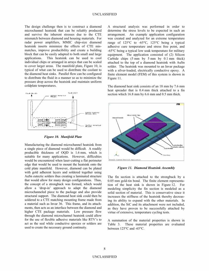
A structural analysis was performed in order to determine the stress levels to be expected in such an arrangement. An example application configuration was created and analyzed for an extreme temperature range of 125�C to -65�C, 125�C being a typical adhesive cure temperature and stress free point, and -65�C being a typical low soak temperature for military equipment. The application consisted of (2) Silicon Carbide chips (5 mm by 5 mm by 0.1 mm thick) attached to the top of a diamond heatsink with AuSn solder. The heatsink was mounted to an Invar package with a silver-loaded, electrically conductive epoxy. A finite element model (FEM) of this system is shown in Figure 11.
The design challenge then is to construct a diamond microchannel heatsink that can be reliably produced and survive the inherent stresses due to the CTE mismatch between diamond and housing materials. For radar power amplifiers, MMIC chip-size diamond heatsink inserts minimize the effects of CTE mis-matches, improve producibility and create a building block that can be easily adapted to both small and large applications. This heatsink can be used to cool individual chips or arranged in arrays that can be scaled to cover larger areas. The manifold plate, Figure 10, is typical of what can be used to distribute the coolant to the diamond heat sinks. Parallel flow can be configured to distribute the fluid in a manner so as to minimize the pressure drop across the heatsink and maintain uniform coldplate temperatures. The diamond heat sink consists of an 18 mm by 7.6 mm
heat spreader that is 0.4 mm thick attached to a fin section which 16.8 mm by 6.6 mm and 0.5 mm thick.
Figure 10. Manifold Plate
Manufacturing the diamond microchannel heatsink from a single piece of diamond would be difficult. A readily producible thickness of OQD is 1.6 mm, which is suitable for many applications. However, difficulties would be encountered when laser-cutting a flat perimeter edge that would be used to mount the heatsink onto the cold plate manifold. However, diamond can be plated with gold adherent layers and soldered together using AuSn eutectic solders thus creating a laminated structure that would allow for many design configurations. Thus, the concept of a strongback was formed, which would allow a ‘drop-in’ approach to adapt the diamond microchanneled piece to the package and also provide structural support. The diamond heat sink could then be soldered to a CTE matching mounting frame made from a material such as Invar 36. This frame, and its attach-ments, then acts as an interface between the diamond and higher CTE package materials. Low pressure flow through the diamond microchannel heatsink could allow for the use of flexible adhesive materials like RTV’s to act as the seal while conductive epoxies or solders are used to create the necessary ground continuity.
Figure 11. Diamond Heatsink Assembly
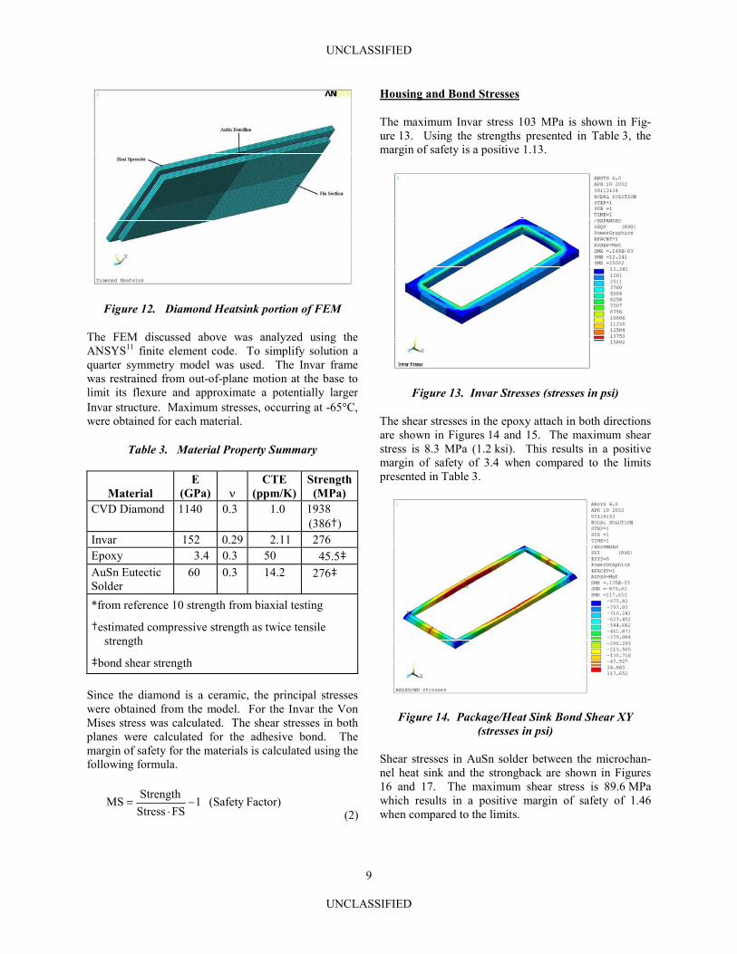
The fin section is attached to the strongback by a 0.05 mm gold-tin bond. The finite element representa-tion of the heat sink is shown in Figure 12. For modeling simplicity the fin section is modeled as a solid section of material. This is conservative since it increases the stiffness of the heatsink thereby decreas-ing its ability to expand with the other materials. In addition, the SiC and its attachment were not included, as they have proven to be successfully attached by virtue of extensive, temperature cycling tests.
A summation of the material properties is shown in Table 3. These material properties are evaluated between 125�C and -65�C.
8
UNCLASSIFIED
UNCLASSIFIED
Housing and Bond Stresses
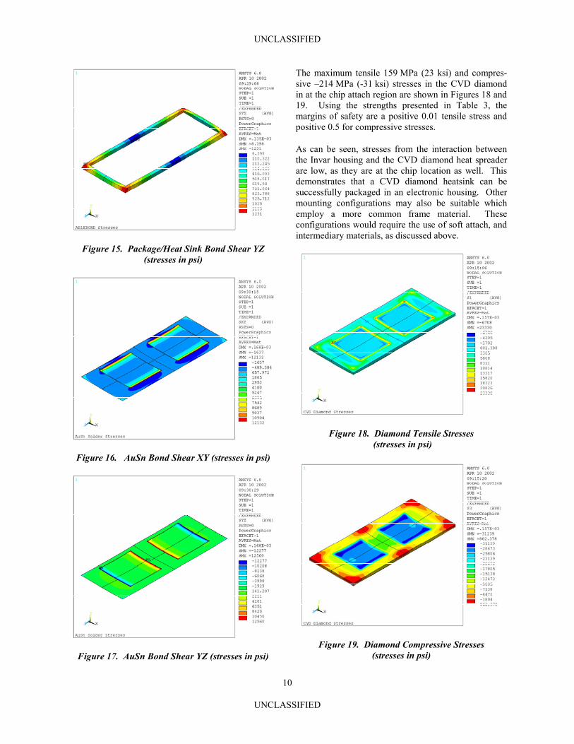
The maximum Invar stress 103 MPa is shown in Fig-ure 13. Using the strengths presented in Table 3, the margin of safety is a positive 1.13.
Figure 12. Diamond Heatsink portion of FEM
The FEM discussed above was analyzed using the ANSYS11 finite element code. To simplify solution a quarter symmetry model was used. The Invar frame was restrained from out-of-plane motion at the base to limit its flexure and approximate a potentially larger Invar structure. Maximum stresses, occurring at -65�C, were obtained for each material.
Figure 13. Invar Stresses (stresses in psi)
Table 3. Material Property Summary
Material E
(GPa) � CTE
(ppm/K)Strength(MPa)
CVD Diamond 1140 0.3 1.0 1938 (386†)
Invar 152 0.29 2.11 276 Epoxy 3.4 0.3 50 45.5‡ AuSn Eutectic Solder
60 0.3 14.2 276‡
*from reference 10 strength from biaxial testing
†estimated compressive strength as twice tensile strength
‡bond shear strength
The shear stresses in the epoxy attach in both directions are shown in Figures 14 and 15. The maximum shear stress is 8.3 MPa (1.2 ksi). This results in a positive margin of safety of 3.4 when compared to the limits presented in Table 3.
Since the diamond is a ceramic, the principal stresses were obtained from the model. For the Invar the Von Mises stress was calculated. The shear stresses in both planes were calculated for the adhesive bond. The margin of safety for the materials is calculated using the following formula.
Figure 14. Package/Heat Sink Bond Shear XY (stresses in psi)
Factor)(Safety 1FSStress
StrengthMS �
�
�
(2)
Shear stresses in AuSn solder between the microchan-nel heat sink and the strongback are shown in Figures 16 and 17. The maximum shear stress is 89.6 MPa which results in a positive margin of safety of 1.46 when compared to the limits.
9
UNCLASSIFIED
UNCLASSIFIED
The maximum tensile 159 MPa (23 ksi) and compres-sive –214 MPa (-31 ksi) stresses in the CVD diamond in at the chip attach region are shown in Figures 18 and 19. Using the strengths presented in Table 3, the margins of safety are a positive 0.01 tensile stress and positive 0.5 for compressive stresses.
As can be seen, stresses from the interaction between the Invar housing and the CVD diamond heat spreader are low, as they are at the chip location as well. This demonstrates that a CVD diamond heatsink can be successfully packaged in an electronic housing. Other mounting configurations may also be suitable which employ a more common frame material. These configurations would require the use of soft attach, and intermediary materials, as discussed above.
Figure 15. Package/Heat Sink Bond Shear YZ (stresses in psi)
Figure 18. Diamond Tensile Stresses (stresses in psi)
Figure 16. AuSn Bond Shear XY (stresses in psi)
Figure 19. Diamond Compressive Stresses (stresses in psi) Figure 17. AuSn Bond Shear YZ (stresses in psi)
10
UNCLASSIFIED
UNCLASSIFIED
11
UNCLASSIFIED
IV. FIRST SAMPLE FABRICATION ACKNOWLEDGMENTS
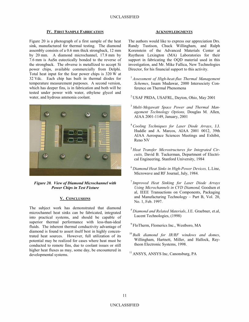
Figure 20 is a photograph of a first sample of the heat sink, manufactured for thermal testing. The diamond assembly consists of a 0.6 mm thick strongback, 12 mm by 20 mm. A diamond microchannel, 17.8 mm by 7.6 mm is AuSn eutectically bonded to the reverse of the strongback. The obverse is metallized to accept Si power chips, available commercially from Delphi. Total heat input for the four power chips is 320 W at 32 Vdc. Each chip has built in thermal diodes for temperature measurement purposes. A second version, which has deeper fins, is in fabrication and both will be tested under power with water, ethylene glycol and water, and hydrous ammonia coolant.
The authors would like to express our appreciation Drs. Randy Tustison, Chuck Willingham, and Ralph Korenstein of the Advanced Materials Center at Raytheon Lexington (MA) Laboratories for their support in fabricating the OQD material used in this investigation, and Mr. Mike Fallica, New Technologies Director, for his financial support to this activity.
1 Assessment of High-heat-flux Thermal Management Schemes, Issam Mudawar, 2000 Intersociety Con-ference on Thermal Phenomena
2 USAF PRDA, USAFRL, Dayton, Ohio, May 2001
3 Multi-Megawatt Space Power and Thermal Man-agement Technology Options, Douglas M. Allen, AIAA 2001-1149, January, 2001
4 Cooling Techniques for Laser Diode Arrays, J.J. Huddle and A. Marcos, AIAA 2001 0012, 39th AIAA Aerospace Sciences Meetings and Exhibit, Reno NV
5 Heat Transfer Microstructures for Integrated Cir-cuits, David B. Tuckerman, Department of Electri-cal Engineering, Stanford University, 1984
6 Diamond Heat Sinks in High-Power Devices, L.Line, Microwave and RF Journal, July, 1984.
7 Improved Heat Sinking for Laser Diode Arrays Using Microchannels in CVD Diamond, Goodsen et al, IEEE Transactions on Components, Packaging and Manufacturing Technology – Part B, Vol. 20, No. 1, Feb. 1997.
Figure 20. View of Diamond Microchannel with Power Chips in Test Fixture
V. CONCLUSIONS
The subject work has demonstrated that diamond microchannel heat sinks can be fabricated, integrated into practical systems, and should be capable of superior thermal performance with less-than-ideal fluids. The inherent thermal conductivity advantage of diamond is found to assert itself best in highly concen-trated heat sources. However, full utilization of its potential may be realized for cases where heat must be conducted to remote fins, due to coolant issues or still higher heat fluxes as may, some day, be encountered in developmental systems.
8 Diamond and Related Materials, J.E. Graebner, et.al, Lucent Technologies, (1998)
9 FloTherm, Flomerics Inc., Westboro, MA
10 Bulk diamond for IR/RF windows and domes, Willingham, Hartnett, Miller, and Hallock, Ray-theon Electronic Systems, 1998.
11 ANSYS, ANSYS Inc, Canonsburg, PA