device simulations of silicon detectors: a design …vertex2002/vprivate/passeri.pdfnmoslvt reset...
TRANSCRIPT

DeviceDevice Simulations of Silicon Simulations of Silicon Detectors: a Design PerspectiveDetectors: a Design Perspective
D. Passeri1,2, P. Placidi1,2, L. Verducci1,2, F. Moscatelli1,2
P. Ciampolini1,3, G. Matrella1,3, A.Marras3, G.M. Bilei1
(3)(3) DipartimentoDipartimento didi Ingegneria dell’InformazioneIngegneria dell’InformazioneUniversità di Parma Università di Parma -- ItalyItaly
(1)(1) Istituto NazionaleIstituto Nazionale didi Fisica Nucleare Fisica Nucleare SezioneSezione di Perugia di Perugia -- ItalyItaly
(2)(2) DipartimentoDipartimento didi Ingegneria ElettronicaIngegneria Elettronica ee dell’Informazionedell’InformazioneUniversità degli Studi di Perugia Università degli Studi di Perugia -- ItalyItaly

OutlineOutline
• Introduction.
• Device-Level Simulation:
- Radiation Damage Analysis.- Design of CMOS Pixel Detectors.
• Conclusions.
- Motivations.- Modeling characteristics.
• Applications (Design Issues):
Device Simulations of Silicon Detectors: a Design Perspective
Vertex 2002

DeviceDevice--Level Simulation: MotivationsLevel Simulation: Motivations• Device simulation:
- numerical solution of semiconductor transport equations;- accurate physical modeling;- distributed domain (spatial, temporal).
• Allows for:- fast and inexpensive prediction of device performance;- microscopic behavior insight;- virtual work-benching and optimization;
• Link between microscopic and macroscopic effects.
Device Simulations of Silicon Detectors: a Design Perspective
Vertex 2002

Device Simulation: Physical ModelsDevice Simulation: Physical Models• Drift-diffusion approximation of current densities.• Radiation-induced carrier-generation term.• Radiation-induced deep-level traps.• Contribution of trapped carriers to the charge density.
• Continuity equations for free and trapped charges.
( ) ( )adADs npnpNNq −+−+−=∇−⋅∇ −+ ϕε
nn UJqt
n −=⋅∇−r1
∂∂
nanaa UJ
qtn −=⋅∇−
r1∂
∂
pp UJqt
p −=⋅∇+r1
∂∂
pdpdd UJ
qtp −=⋅∇+
r1∂
∂
Device Simulations of Silicon Detectors: a Design Perspective
Vertex 2002

Radiation Damage AnalysisRadiation Damage Analysis• Deep-level radiation induced traps:
- Nt, Et, σn, σp
• SRH statistics.• Donor removal.• Hierarchical approach:
- complexity/comprehensiveness; - accurate prediction of device behavior;- most parameters physically meaningful; - experimental characterization feasible.
Device Simulations of Silicon Detectors: a Design Perspective
Vertex 2002

Radiation Damage ModelingRadiation Damage Modeling• The model should allow for reproducing the electrical behavior of heavily
irradiated device in terms of:- effective doping concentration depending on fluence;- depletion region profiles;- increase of the leakage current;- charge collection reduction.
• Enhanced, device-level radiation damage modeling scheme featuring:- four “dominant” deep levels (related to V2
(-/0), CiOi, V2O, E(70)).- donor removal mechanism (c*ND = 0.05 cm-1).- direct charge exchange between V2
(-/0) and E(70).• All parameters are physically meaningful and experimentally characterized.
• Suitable for use within general purpose device simulators (i.e. spatial and time-domain analysis feasible).
Device Simulations of Silicon Detectors: a Design Perspective
Vertex 2002

Radiation Damage Modeling (2)Radiation Damage Modeling (2)
0.41•10-15
1•10-14
Ec- 0.45E70
1•10-151•10-161•10-16σn [cm2]
Ev+ 0.36Ec- 0.50Ec- 0.42E [eV]
10.081η [cm-1]
1•10-161•10-152•10-15σp [cm2]
CiOi+/0V2O0/-V2
0/-Parameter
1•10-151•10-161•10-16σn [cm2]
Ev+ 0.36Ec- 0.50Ec- 0.42E [eV]
10.0826η [cm-1]
1•10-161•10-158•10-15σp [cm2]
CiOi+/0V2O0/-V2
0/-Parameter
• Higher computational effort
• Computational limitations for off-range conditions:
- high fluences (> 1014 n/cm2)- low temperature.
Device Simulations of Silicon Detectors: a Design Perspective
Vertex 2002
• Fitted values of V2 parameters to reproduce the “cluster effect”.
•Suitable for high fluences and low temperature analyses.
Four levels Vs. three levels modelingDirect charge exchange

Radiation Damage Modeling ApplicationsRadiation Damage Modeling Applications
Comparison between predictions of ISE-TCAD three-level model (squares) and experimental data (circles) for Neff as a function of neutronfluence.
Experimental data and predictions of ISE-TCAD three-level model for Neff as a function of temperature for an irradiated device (6.2•1013 1MeV n).
Device Simulations of Silicon Detectors: a Design Perspective
Vertex 2002

nMOSlvt
RESET
pMOSstdRESET
pMOSstd
VFTD
• Assessment of CMOS deep submicron technology suitability for fabricationof charged particle detectors.
• Optimization of the sensitive element.
• Innovative active pixel detection scheme: the WIPS idea.
Design of CMOS Pixel DetectorsDesign of CMOS Pixel Detectors
Device Simulations of Silicon Detectors: a Design Perspective
Vertex 2002

nMOSlvt
RESET
pMOSstd
RESET
pMOSstd
VFTD
The WIPS Pixel SensorThe WIPS Pixel Sensor VDD
C3
C2
CUP
OUT_COL
C1
C0CDOWN
OUT_ROW
VDD
VFTD is charged-up through a RESET pulse.
The VFTD voltage is raised up toVFTD = VDD-|VTp|
(with VTn < |VTp|).
If a particle hit occurs, VFTD ↓, pMOS goes ON…
A conductive path allows for the charge of CDOWN.
1
3 2
4
To the COL amplifier...
To the ROW amplifier...
Part
icle
hit
Device Simulations of Silicon Detectors: a Design Perspective
Vertex 2002
• Device/Circuit analysis.

RAPS01 Chip LayoutRAPS01 Chip Layout
Device Simulations of Silicon Detectors: a Design Perspective
Vertex 2002
• 0.18 µm CMOS technology. • 1.8/3.3 V.• A/D VLSI design.• 11 APS matrices.• 8 WIPS matrices.• 8 main test structures.

WIPS WIPS DeviceDevice--Level AnalysisLevel Analysis
A
A’
B
B’
n-well
n-well
n-well n-well
BB’
AA
’
p-wellp-well
Device Simulations of Silicon Detectors: a Design Perspective
Vertex 2002
123
C’C
CC’
n-well n-well

WIPS DeviceWIPS Device--Level Analysis (2)Level Analysis (2)Current responses of the “sensitive elements” (n-wells) to a particle hitdepending on the particle trajectory (AA’ section).
Track # 1 Track # 2 Track # 3
Time [sec] Time [sec] Time [sec]
Curr
ent
[A]
Curr
ent
[A]
Curr
ent
[A]
Device Simulations of Silicon Detectors: a Design Perspective
Vertex 2002
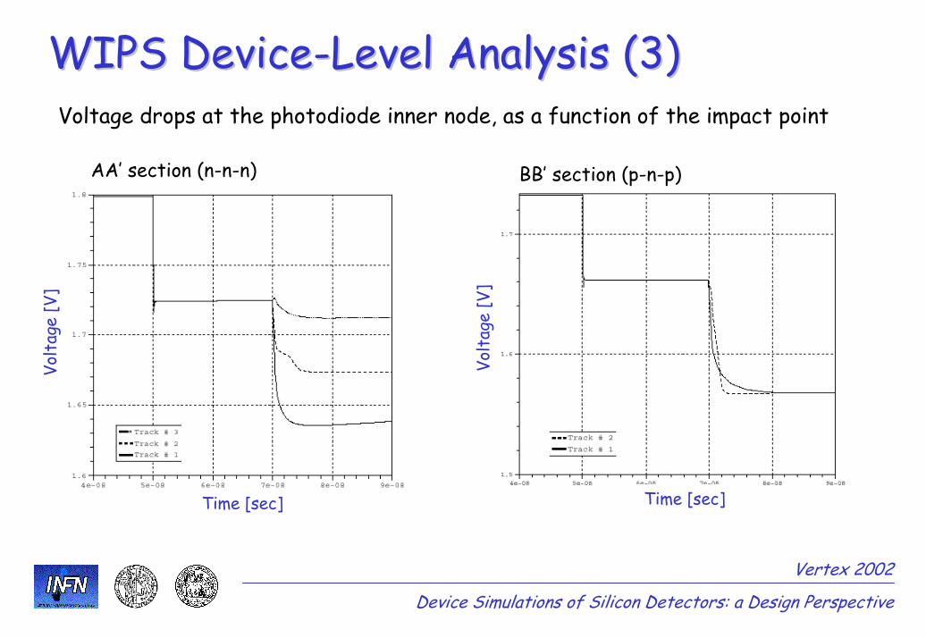
WIPS DeviceWIPS Device--Level Analysis (3)Level Analysis (3)
Device Simulations of Silicon Detectors: a Design Perspective
Vertex 2002
Voltage drops at the photodiode inner node, as a function of the impact point
AA’ section (n-n-n) BB’ section (p-n-p)
Volt
age
[V]
Volt
age
[V]
Time [sec]Time [sec]

WIPS DeviceWIPS Device--Level Analysis (Level Analysis (44))
Device Simulations of Silicon Detectors: a Design Perspective
Vertex 2002
Voltage drops at the photodiode inner nodes (CC’ section)
Volt
age
[V]
Time [sec]
Volt
age
[V]
Time [sec]
hit pixel
adjacent pixel
no guardring guardring

WIPS WIPS Circuit AnalysisCircuit Analysis
V OU
T_RO
W[V
]
ROW Analog Output
Dark rows
Hit row
∆V = 238 mV
COL Analog Output
Time [s]
V OU
T_CO
L[V
]
Time [s]
∆V = 670 mV
Hit col
Dark cols
Device Simulations of Silicon Detectors: a Design Perspective
Vertex 2002

DIF
F_A
MPL
IFIE
R
COL_EN
NEG_COL_EN
64
64
ANALOG_OUT
X
RO
W_E
N
NEG
_EO
W_E
N6464
DIFF_AMPLIFIER
ENABLE_BUFFER
32CTRL_0
32CTRL_1
32CTRL_2
32CTRL_3
32RESET
RIF_RIGA
POL_SPECCHIO
RIF_COL
RIF_COLUMN
POL_MIRROR
RIF_ROW ……
…
WPS_32x32G0P0
WIPS WIPS Matrix ArchitectureMatrix Architecture
• Single row scan / serial out: (n + n ) x TCLOCK
• Pixel size 10 x 10 µm2
Device Simulations of Silicon Detectors: a Design Perspective
ConclusionsConclusionsNumerical device-level simulation has been assessed as powerful tool for analysis and design of particle detectors.
A comprehensive, device-level radiation damage modeling scheme, based on a hierarchical approach, has been devised, allowing for a broad range of application issues.Coupled device- and circuit-level analyses have been extensively exploited within a conventional CMOS VLSI design flow for the realization of innovative pixel detectors.
Fast and inexpensive performance prediction, as well as physical and intuitive interpretation of device behavior can be obtained.
Device Simulations of Silicon Detectors: a Design Perspective
Vertex 2002