development of the advanced deep space transponder · development of the advanced deep space...
TRANSCRIPT

IPN Progress Report 42-156 February 15, 2004
Development of the Advanced DeepSpace Transponder
B. Cook,1 M. Dennis,1 S. Kayalar,2 J. Lux,1 and N. Mysoor1
We present the architecture and design of a new transponder to support deep-space and near-Earth missions in the post-2010 time frame. This transponder isdesigned to provide direct-to-Earth command and telemetry service; spacecraft-to-spacecraft command and telemetry service; direct-to-Earth navigation in theform of coherent Doppler turnaround, sequential turn-around ranging, pseudo-noiseregenerative ranging, and differential one-way ranging; and spacecraft-to-spacecraftnavigation in the form of coherent Doppler turnaround and one-way pseudo-noisecode ranging.
I. Introduction
All JPL deep-space missions currently use transponders to provide direct-to-Earth communicationsand navigation services. In addition, some missions equip the transponder with an ultra-stable oscillator(USO) and use the transponder as an instrument for radio science. The transponder currently in use,the Small Deep Space Transponder (SDST),3 manufactured at General Dynamics Decision Systems, wasdesigned in 1992 using the technology available at the time. Over 10 years later, electronics parts usedin the design are becoming obsolete, we are running out of digital application-specific integrated circuits(ASICs) from the original foundry run, and it is clear that the SDST will not be able to support newmissions for more than a few more years.
As part of an effort to replace the SDST for missions scheduled in the 2010 time frame and beyond, weembarked upon a research and technology development task in 2003 to put together an architecture forthe next-generation transponder and to develop the digital signal-processing capabilities needed by futuremissions. In this article, we will discuss our progress on this ongoing task. We will present our designrationale, the functional and performance requirements on which we are basing our architecture, somesignal-processing design analysis, and experimental results we have achieved to date with a prototyperadio-frequency front end and digital development platform.
1 Spacecraft Telecommunications Equipment Section.
2 Communications Systems and Research Section.
3 Small Deep Space Transponder Group Buy Specification, Rev. B, JPL ES-518193 (internal document), Jet PropulsionLaboratory, Pasadena, California, August 2001.
The research described in this publication was carried out by the Jet Propulsion Laboratory, California Institute ofTechnology, under a contract with the National Aeronautics and Space Administration.
1
II. Design Rationale
In the formulation of the architecture of the Advanced Transponder, we were guided by the design goalsenumerated in the following subsections. In all cases, we have tried to make maximum use of the designheritage of the Cassini Deep Space Transponder (DST),4 the Small Deep Space Transponder (SDST),and the JPL Spacecraft Transponding Modem (STM) [1], which unfortunately was not completed.
A. Preservation of Function and Performance
Our starting point in this effort was that we would not reduce the functionality or degrade the per-formance of the existing SDST. Rather, all new functionality would serve to enhance performance whilepreserving the specifications to which current missions are designing. In the process of developing thisdesign, we have come upon a few areas in which we may want to make compromises. These areas arelisted here and described in more detail in later sections:
(1) Radio Science: The downlink carrier stability requirements for radio science are designdrivers and may be difficult to meet given our new frequency-agile front-end architecture. Ifwe find that we cannot meet these requirements with our generic architecture, our modulardesign will allow us to develop a front-end module specifically for radio science that meetsthe stability requirements at the expense of some tuning-range capability. In other words,radio science may require a dedicated front-end module, which can be developed for missionsspecifically requiring that function.
(2) Downlink Telemetry Encoding: The SDST provides a wide range of convolutional encodingmode options although the only options ever used in flight have been 7-1/2 and 15-1/6non-return-to-zero-level (NRZ L). We are considering eliminating the other convolutionalencoding options, especially because we will be implementing turbo coding as a downlinkoption.
B. Reduction of Power, Weight, and Manufacturing Cost
The current SDST (in the Mars Exploration Rover 8.4-GHz (X-band) downlink-only configuration)weighs about 2.6 kg, draws about 14 W while transmitting,5 and involves large recurring engineeringproduction costs, largely because of hand tuning of a large number of RF components and the use ofrelatively low-yield RF multi-chip modules (MCMs). Our approach in this effort has been to push muchof the functionality into the digital realm, eliminating secondary analog downconversion stages, andsimplifying the RF architecture. We also have identified radio frequency integrated circuits (RFICs) ormonolithic microwave integrated circuits (MMICs) that either are in development or could be developedthat would allow elimination of the multi-chip modules that account for much of the touch labor, boardarea, and design risk in the SDST. With these changes, we are anticipating at least a 50 percent reductionin mass, power, and unit production cost.
C. Support of Spacecraft Crosslinks as well as Direct-to-Earth Links
A major enhancement to the functionality of the DST, SDST, and STM is the addition of spacecraftcrosslink, or spacecraft-to-spacecraft, communications and navigation service. As future solar systemexploration programs send multiple spacecraft to a single target or fly constellations of spacecraft, we willneed to support data relay and exchange of information between multiple spacecraft. In addition, as werequire greater landing precision, we need to rely on assets in orbit around a target to enhance navigationby providing Doppler measurement and pseudo-noise (PN) ranging sessions with an approaching lander
4 Deep Space Transponder Specification, JPL FM 513778 (internal document), Jet Propulsion Laboratory, Pasadena, Cali-fornia, March 1994.
5 Mars Exploration Rover Hardware Review/Certification Requirements (HRCR) 1001, MER 420-3-480 (internal docu-ment), Jet Propulsion Laboratory, Pasadena, California, February 2002.
2
in directions orthogonal to the Earth–probe line of sight. We have incorporated this functionality intothe architecture of the Advanced Transponder.
D. Increase in Data Throughput
To support the increased data volumes of future missions, our goal is to extend the downlink telemetryrate to 100 Mb/s, which would be available as a quadrature phase-shift keying (QPSK) modulation modeat 32-GHz (Ka-band) downlink frequencies (since the X-band allocation does not support this wide of abandwidth). To support large software uploads and data relay services, we will extend the uplink datarate capability to 256 kb/s, up from the 2 kb/s maximum rate supported by the SDST and STM.
E. Incorporation of Key Telecommunications–Avionics Functions
Another goal behind the development of this architecture is the incorporation into the transponder ofkey telecommunications functions that have traditionally been performed in avionics:
(1) Command Code Block Processing. The synchronized uplink bit stream is scanned for the0xEB90 start sequence, and command code blocks are decoded, validated using the cyclicredundancy check codes, and then transferred to avionics as a validated code block.
(2) Hardware Command Decoding. As part of the command decoding process, virtual-channel-0commands are identified, and the indicated latching relay is set or cleared.
(3) Downlink Turbo and Reed–Solomon Encoding. Data are transferred from avionics to thetransponder as a complete frame. The transponder then performs Reed–Solomon plus con-volutional encoding or turbo encoding on the full frame as requested and then downlinksthe frame.
The result of these architectural changes, as compared to the SDST baseline, is that the interfacebetween the transponder and avionics becomes a frame-level rather than a bit-level interface. Thiseliminates the need for synchronous data–clock–lock interfaces and allows the command and telemetrypaths to share a single high-rate interface with the transponder mode control and data interface. Thischange also eliminates the need for special Reed–Solomon and turbo encoding software and hardware, aswell as hardware command decoder hardware, on the avionics side, freeing up spacecraft system resourcesthat can be applied instead to science data processing.
F. Built-In Redundancy and Modular Design
In order to simultaneously support a direct-to-Earth (DTE) link and a spacecraft crosslink, and to buildin functional redundancy, we have targeted a modular architecture allowing interchangeability betweenthe DTE and crosslink baseband digital processors, as well as between optional RF front ends operatingat 2.2 GHz (S-band), 8.4 GHz (X-band), or 32 GHz (Ka-band).
In this design, two identical baseband processors operate in parallel, one targeted for DTE and theother for crosslink. At the time of manufacture, two switchable RF front-end modules are selected foreach baseband processor. For example, an X-band and a Ka-band module might be selected for the DTEchannel, and a normal and an inverted S-band module might be selected for the crosslink channel. Inthe case of a DTE channel failure, the S-band crosslink channel, which supports identical digital signalprocessing, could be used for backup communications with the Deep Space Network (DSN). A moredetailed look at this architecture is presented in Section III.
G. Design of a Frequency-Agile Front End
Another key goal in this development is to provide a frequency-agile front end that can be tuned inflight to cover all channels in the DSN band allocation. The current SDST is assigned a channel frequencyat time of manufacture by the selection of a crystal oscillator and other frequency-specific parts. This
3

makes the sharing of spare units between projects particularly difficult if they are operating with differentfrequency assignments.
The challenge in implementing this tunability is that the required reduction in the quality factor(Q) of the dielectric resonance oscillator phase-locked loop (DRO-PLL) could degrade the phase noiseperformance of the carrier-tracking and downlink synthesis loops. However, preliminary laboratory workwith the STM DRO [2] design indicates that the Q of the DRO is not the primary contributor to thephase noise, and we do not see significant degradation due to the increased coupling. These results arepresented later in this article. In addition, the narrow bandwidth of the digital carrier-tracking loop canbe maintained in order to preserve the low uplink signal detection threshold.
H. Addition of New Signal-Processing Functions
Finally, another driving goal is to incorporate enhanced digital signal processing in order to provideadditional functionality over what the current SDST provides. New functions included in this designinclude the following:
(1) Pseudo-Noise (PN) Regenerative Ranging. By synchronizing to and regenerating a pseudo-noise ranging signal onboard, we can dramatically improve ranging performance. For atypical Mars mission, this improvement is estimated to be about 17 dB [3].
(2) Crosslink PN Ranging. For spacecraft-to-spacecraft navigation, the same PN correlatorused for direct-to-Earth navigation can be applied to measuring the phase of an arriving PNsignal from another spacecraft. With exchange of clock information over the communicationschannel, these data can be used to calculate range information. At the 1-MHz chip rate usedfor DTE navigation, and using a 20-MHz processing clock, we expect to achieve a resolutionof less than 20 m. It also may be possible to get sub-clock-edge resolution by integrationover many clock cycles.
(3) Quadrature Phase-Shift Keying (QPSK) Downlink Modulation. We have incorporated botha linear phase modulator and a QPSK modulator into this design to support high-rate signal-ing on the downlink. Note that the SDST to be flown on the Mars Reconnaissance Orbiter(MRO) has also included QPSK modulation as an upgrade in the form of an additional fieldprogrammable gate array (FPGA).
(4) Phase-Shift Keying (PSK) Command Demodulator. In order to receive high-rate uplink, wehave incorporated a PSK uplink demodulator in addition to the traditional command detec-tion unit (CDU) from the SDST. The PSK demodulator enables crosslink communicationsby providing a receiver that is compatible with the PSK downlink modulation format usedby the SDST and by the Advanced Transponder.
III. Transponder Architecture
Our goals in this research effort were to push the RF–digital boundary further toward the digital side,to create a modular and interchangeable front-end design, to identify and specify RF components to beprocured or developed, and to provide flexibility and programmability in the digital signal processing.This section provides a detailed description of the architecture developed during the first year of thisresearch task.
A. Modular Functional Partitioning
The key aspect of the front-end design is the identification of configurable RF modules that can becombined at time of manufacture with the same digital back end in order to provide mission-specificperformance and functional redundancy. Three key frequency bands were identified for development:Ka-band, X-band, and S-band. Ka-band, operating at 34 GHz and 32 GHz for uplink and downlink,
4
respectively, is an enabling communication band for future high-data-rate missions requiring more databandwidth than can be supported at X-band. X-band, at 7.1 GHz and 8.4 GHz for uplink and downlink,respectively, provides backward compatibility for current missions, is fully supported by all Deep SpaceNetwork stations, and provides good emergency-rate downlink and practical low-gain performance formissions that lose or do not have the capability to accurately point a Ka-band antenna. S-band, at2.1 GHz and 2.2 GHz for uplink and downlink, respectively, is primarily used in this architecture as arelay channel for crosslink spacecraft-to-spacecraft communication. In addition, because the DSN stillsupports S-band communications, this channel can be used as a functional backup for direct-to-Earthcommunications.
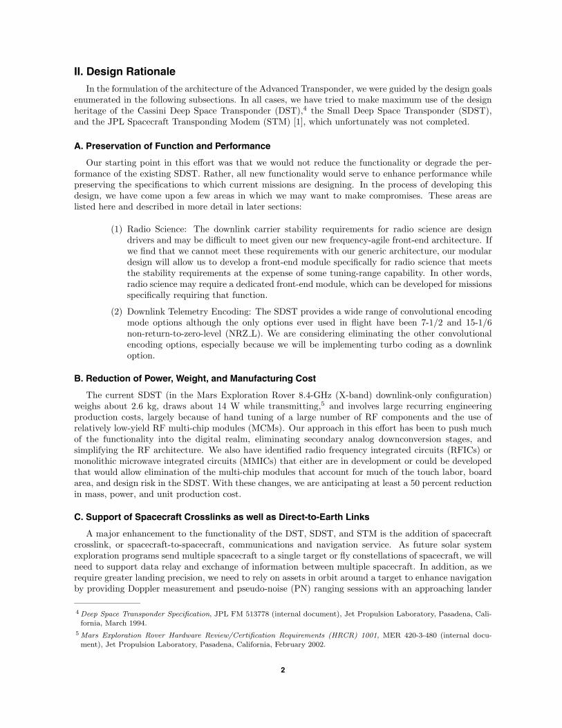
The architecture we have developed allows for the simultaneous operation of two separate two-waycoherent front ends. In addition, each of these two channels can be switched to one of two separate RFmodules, providing four available front ends, two of which can be used simultaneously. Figure 1 providesan overview of this front-end architecture.
The digital processing back ends for the DTE link and crosslink channels are identical and can be usedinterchangeably for either function. This provides built-in functional redundancy to increase reliabilityand potentially eliminate the need for some missions to fly two transponders.
INVX
INVKa
INVSS
Ka
X
A/D
DAC
A/D
DAC
DigitalProcessor
A
DigitalProcessor
B
8.4GHz
7.1GHz
X-Band RX TX
32GHz
34GHz
Ka-Band RX TX
2.2GHz
2.1GHz
S-Band RX TX
INV S-Band Rx Tx
2.1GHz
2.2GHz
INV Ka-Band Rx Tx
34GHz
32GHz
INV X-Band Rx Tx
7.1GHz
3.4GHz
Fig. 1. Modular front-end architecture, illustrating dual parallel digital processors and four selectable RFfront-end modules, each of which can be configured at manufacture time to one of six possible front ends:S-band, X-band, or Ka-band, or channel-inverted S-band, X-band, or Ka-band. The most common configuration(X-band and Ka-band for DTE and S-band and inverted S-band for crosslink) is shown.
5
B. RF Front-End Architecture
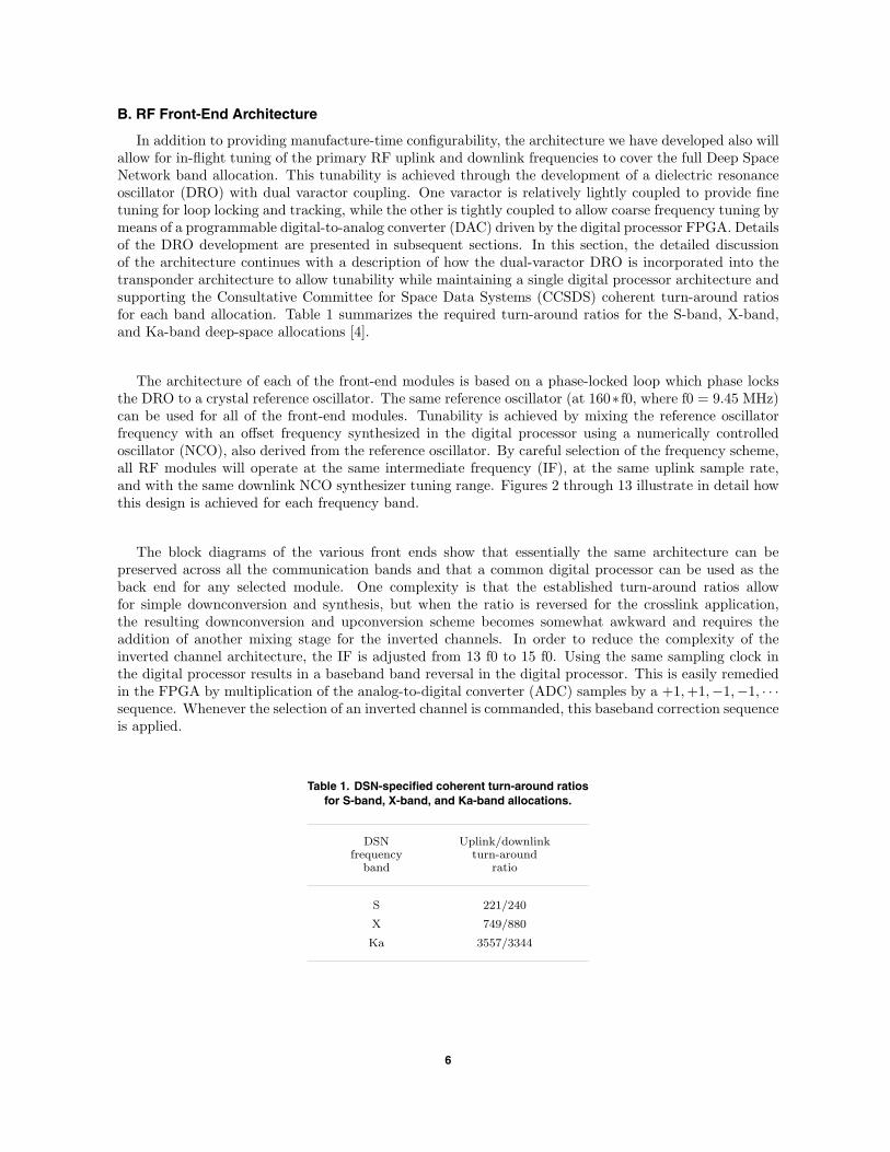
In addition to providing manufacture-time configurability, the architecture we have developed also willallow for in-flight tuning of the primary RF uplink and downlink frequencies to cover the full Deep SpaceNetwork band allocation. This tunability is achieved through the development of a dielectric resonanceoscillator (DRO) with dual varactor coupling. One varactor is relatively lightly coupled to provide finetuning for loop locking and tracking, while the other is tightly coupled to allow coarse frequency tuning bymeans of a programmable digital-to-analog converter (DAC) driven by the digital processor FPGA. Detailsof the DRO development are presented in subsequent sections. In this section, the detailed discussionof the architecture continues with a description of how the dual-varactor DRO is incorporated into thetransponder architecture to allow tunability while maintaining a single digital processor architecture andsupporting the Consultative Committee for Space Data Systems (CCSDS) coherent turn-around ratiosfor each band allocation. Table 1 summarizes the required turn-around ratios for the S-band, X-band,and Ka-band deep-space allocations [4].
The architecture of each of the front-end modules is based on a phase-locked loop which phase locksthe DRO to a crystal reference oscillator. The same reference oscillator (at 160∗ f0, where f0 = 9.45 MHz)can be used for all of the front-end modules. Tunability is achieved by mixing the reference oscillatorfrequency with an offset frequency synthesized in the digital processor using a numerically controlledoscillator (NCO), also derived from the reference oscillator. By careful selection of the frequency scheme,all RF modules will operate at the same intermediate frequency (IF), at the same uplink sample rate,and with the same downlink NCO synthesizer tuning range. Figures 2 through 13 illustrate in detail howthis design is achieved for each frequency band.
The block diagrams of the various front ends show that essentially the same architecture can bepreserved across all the communication bands and that a common digital processor can be used as theback end for any selected module. One complexity is that the established turn-around ratios allowfor simple downconversion and synthesis, but when the ratio is reversed for the crosslink application,the resulting downconversion and upconversion scheme becomes somewhat awkward and requires theaddition of another mixing stage for the inverted channels. In order to reduce the complexity of theinverted channel architecture, the IF is adjusted from 13 f0 to 15 f0. Using the same sampling clock inthe digital processor results in a baseband band reversal in the digital processor. This is easily remediedin the FPGA by multiplication of the analog-to-digital converter (ADC) samples by a +1,+1,−1,−1, · · ·sequence. Whenever the selection of an inverted channel is commanded, this baseband correction sequenceis applied.
Table 1. DSN-specified coherent turn-around ratiosfor S-band, X-band, and Ka-band allocations.
DSN Uplink/downlinkfrequency turn-around
band ratio
S 221/240
X 749/880
Ka 3557/3344
6
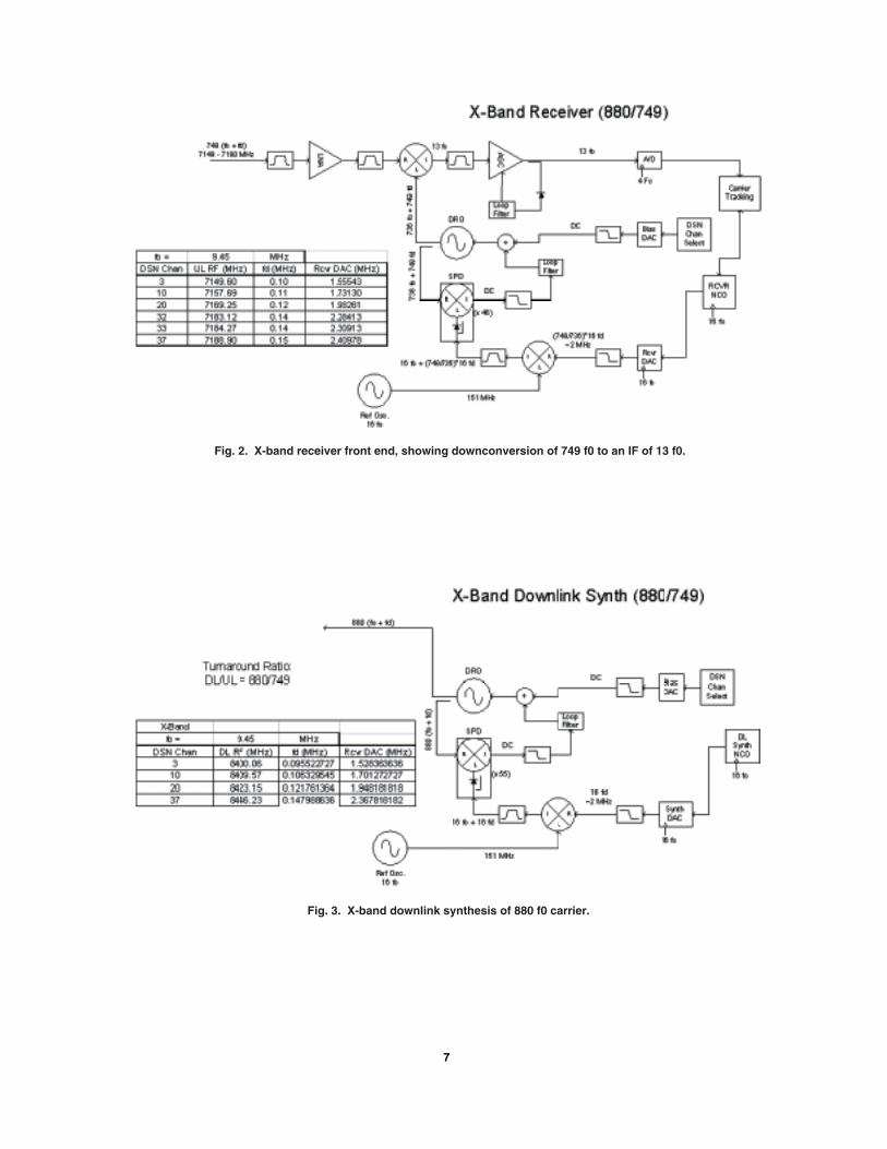
Fig. 2. X-band receiver front end, showing downconversion of 749 f0 to an IF of 13 f0.
Fig. 3. X-band downlink synthesis of 880 f0 carrier.
7
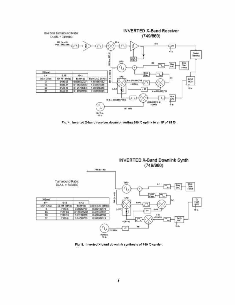
Fig. 4. Inverted X-band receiver downconverting 880 f0 uplink to an IF of 15 f0.
Fig. 5. Inverted X-band downlink synthesis of 749 f0 carrier.
8

Fig. 6. Ka-band receiver front end downconverting 3597 f0 uplink to an IF of 13 f0.
Fig. 7. Ka-band downlink synthesis of 3344 f0 carrier.
9
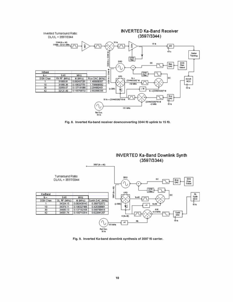
Fig. 8. Inverted Ka-band receiver downconverting 3344 f0 uplink to 15 f0.
Fig. 9. Inverted Ka-band downlink synthesis of 3597 f0 carrier.
10

Fig. 10. S-band uplink downconversion of 221 f0 uplink to an IF of 13 f0.
Fig. 11. S-band downlink synthesis of 240 f0 carrier.
11

Fig. 12. Inverted S-band receiver downconverting 240 f0 uplink to 15 f0.
Fig. 13. Inverted S-band downlink synthesizer generating 221 f0 carrier.
12
C. Digital Processing Architecture
As illustrated in the block diagrams of the RF front-end modules, uplink downconversion proceeds ina single step to an IF of 13 f0 (or 15 f0). The DRO-PLL tracking loop is actually closed inside the digitalprocessor using an NCO to generate an offset frequency to mix with the reference oscillator and lock theDRO loop.
The 13 f0 IF is digitized by an analog-to-digital converter clocked at 4 f0 to produce quadraturebaseband in-phase (I) and quadrature-phase (Q) samples. In lock, the Q samples have zero carriercomponent, and the I samples will be integrated and compared to a threshold to determine lock status.The uplink ranging and command modulation will appear on the Q channel, which will be integratedand routed to the standard command detection unit, the high-rate PSK command decoder, and to theranging processor.
The I and Q samples are used to generate a total signal strength estimate [√
(I2 + Q2)], which is usedfor coherent automatic gain control (AGC) to scale the I samples driving a second-order tracking-loopfilter, the output of which controls the frequency of the receiver NCO, closing the receiver tracking loop.
The frequency and phase of the receiver NCO is digitally locked to a second NCO, which is used todrive the downlink synthesis loop. This downlink offset frequency reference is generated by direct digitalsynthesis and applied to the sampling phase detector to lock the downlink DRO-PLL synthesis loop.
Figure 14 provides a block diagram of the digital tracking and downlink synthesis signal processing.Note that the receiver NCO and synthesis NCO are shown driving a sine look-up table and digital-to-analog converter (DAC). In Section VII, experimental data are presented to illustrate a novel methodby which the DAC and subsequent mixing stages may be eliminated by digital multiplication and directdigital drive of the sampling phase detector.
IV. RF Component Specifications and Analysis
A. X-Band Receiver and Transmitter RF Components
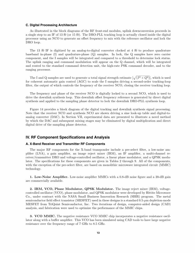
The major RF components for the X-band transponder include a pre-select filter, a low-noise am-plifier (LNA), a gain amplifier, an image reject mixer (IRM), an IF amplifier, a multi-channel re-ceiver/transmitter DRO and voltage-controlled oscillator, a linear phase modulator, and a QPSK modu-lator. The specifications for these components are given in Tables 2 through 9. All of the components,with the exception of the pre-select filter, are based on monolithic microwave integrated circuit (MMIC)technology.
1. Low-Noise Amplifier. Low-noise amplifier MMICs with a 0.8-dB noise figure and a 20-dB gainare commercially available.
2. IRM, VCO, Phase Modulator, QPSK Modulator. The image reject mixer (IRM), voltage-controlled oscillator (VCO), phase modulator, and QPSK modulator were developed by Hittite MicrowaveCo., under contract with the NASA Small Business Innovation Research (SBIR) program. The metalsemiconductor field effect transistor (MESFET) used in these designs is a standard 0.5-µm depletion-modeMESFET from TriQuint Semiconductor, Inc. Two iterations of design, computer-aided design (CAD)analysis, and fabrication were used to optimize the performance of the MMIC chips.
3. VCO MMIC. The negative resistance VCO MMIC chip incorporates a negative resistance oscil-lator along with a buffer amplifier. This VCO has been simulated using CAD tools to have large negativeresistance over the frequency range of 7 GHz to 8.5 GHz.
13
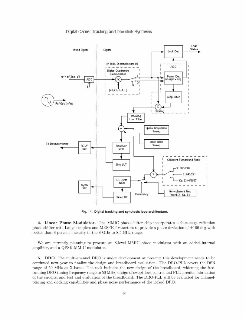
Fig. 14. Digital tracking and synthesis loop architecture.
4. Linear Phase Modulator. The MMIC phase-shifter chip incorporates a four-stage reflectionphase shifter with Lange couplers and MESFET varactors to provide a phase deviation of ±100 deg withbetter than 8 percent linearity in the 8-GHz to 8.5-GHz range.
We are currently planning to procure an S-level MMIC phase modulator with an added internalamplifier, and a QPSK MMIC modulator.
5. DRO. The multi-channel DRO is under development at present; this development needs to becontinued next year to finalize the design and breadboard evaluation. The DRO-PLL covers the DSNrange of 50 MHz at X-band. The task includes the new design of the breadboard, widening the free-running DRO tuning frequency range to 50 MHz, design of swept-lock control and PLL circuits, fabricationof the circuits, and test and evaluation of the breadboard. The DRO-PLL will be evaluated for channel-placing and -locking capabilities and phase noise performance of the locked DRO.
14

Table 2. Multi-channel receiver/transmitter DRO specification.
DRO parameter Specification
X-band RF frequency range:X-band receive DRO frequency range ∼7019 MHz to 7069 MHz
X-band transmit DRO frequency range ∼8400 MHz to 8450 MHz
Course electronic tuning range (receiver) TBD: ∼7039 MHz ± 25 MHz
Fine tuning range (PLL capture range) ±2 MHz
Tuning linearity ±10% or better
Output power level +10 dBm ± 1.0 dB
Free-running DRO SSB phase noise < −50 dBc/Hz at 1 KHz off carrier
Frequency stability versus temperature ±2 ppm/deg C max
Frequency pushing (±5% Vdc) 100 kHz max
Frequency pulling (2:1 voltage standing 100 kHz maxwave ratio (VSWR) all phases)
Harmonics < −33 dBc
Spurious signals < −80 dBc
Operating temperature range −55 deg C to +75 deg C
Output impedance 50 ± 5 ohms, nominal
DC bias current at +5V DC 30 mA
Course electronic tuning control voltage +3 V ± 2 V max
Fine tuning control voltage +3V ± 2 V max
Table 3. Pre-select filter specification.
Pre-select filter parameter Specification
RF frequency range 7148 to 7195 MHz
Insertion loss <0.4 dB
Gain flatness ±0.1 dB, nominal
0.25 dB bandwidth 7170 ± 22 MHz
3 dB bandwidth 7170 ± 25 MHz
Input impedance 50 ± 5 ohms, nominal
Input VSWR 1.2:1
Output impedance 50 ± 5 ohms, nominal
Output VSWR 1.5:1
Operating temperature range −55 deg C to +75 deg C
15
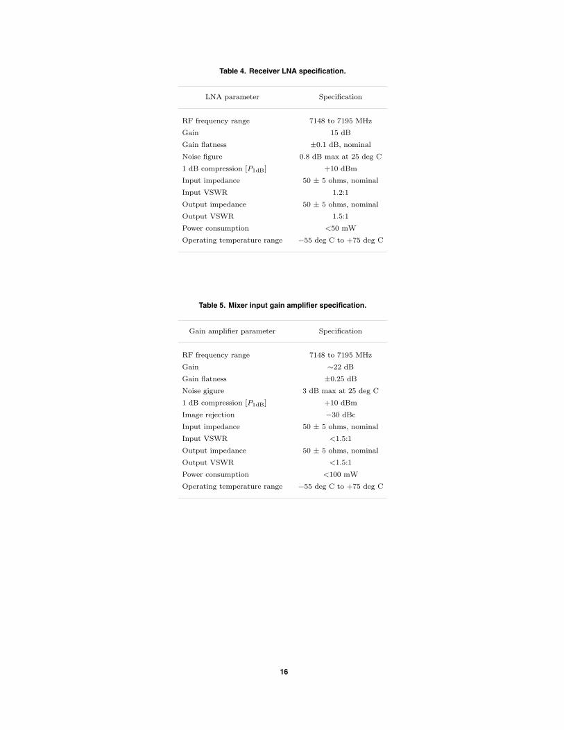
Table 4. Receiver LNA specification.
LNA parameter Specification
RF frequency range 7148 to 7195 MHz
Gain 15 dB
Gain flatness ±0.1 dB, nominal
Noise figure 0.8 dB max at 25 deg C
1 dB compression [P1dB] +10 dBm
Input impedance 50 ± 5 ohms, nominal
Input VSWR 1.2:1
Output impedance 50 ± 5 ohms, nominal
Output VSWR 1.5:1
Power consumption <50 mW
Operating temperature range −55 deg C to +75 deg C
Table 5. Mixer input gain amplifier specification.
Gain amplifier parameter Specification
RF frequency range 7148 to 7195 MHz
Gain ∼22 dB
Gain flatness ±0.25 dB
Noise gigure 3 dB max at 25 deg C
1 dB compression [P1dB] +10 dBm
Image rejection −30 dBc
Input impedance 50 ± 5 ohms, nominal
Input VSWR <1.5:1
Output impedance 50 ± 5 ohms, nominal
Output VSWR <1.5:1
Power consumption <100 mW
Operating temperature range −55 deg C to +75 deg C
16
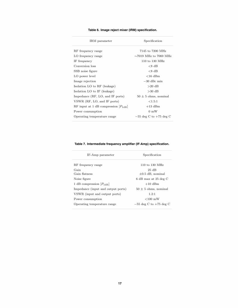
Table 6. Image reject mixer (IRM) specification.
IRM parameter Specification
RF frequency range 7145 to 7200 MHz
LO frequency range ∼7019 MHz to 7069 MHz
IF frequency 110 to 130 MHz
Conversion loss <8 dB
SSB noise figure <8 dB
LO power level <16 dBm
Image rejection −30 dBc min
Isolation LO to RF (leakage) >20 dB
Isolation LO to IF (leakage) >30 dB
Impedance (RF, LO, and IF ports) 50 ± 5 ohms, nominal
VSWR (RF, LO, and IF ports) <1.5:1
RF input at 1 dB compression [P1dB] +13 dBm
Power consumption 0 mW
Operating temperature range −55 deg C to +75 deg C
Table 7. Intermediate frequency amplifier (IF-Amp) specification.
IF-Amp parameter Specification
RF frequency range 110 to 130 MHz
Gain 25 dBGain flatness ±0.5 dB, nominal
Noise figure 6 dB max at 25 deg C
1 dB compression [P1dB] +10 dBm
Impedance (input and output ports) 50 ± 5 ohms, nominal
VSWR (input and output ports) 1.2:1
Power consumption <100 mW
Operating temperature range −55 deg C to +75 deg C
17
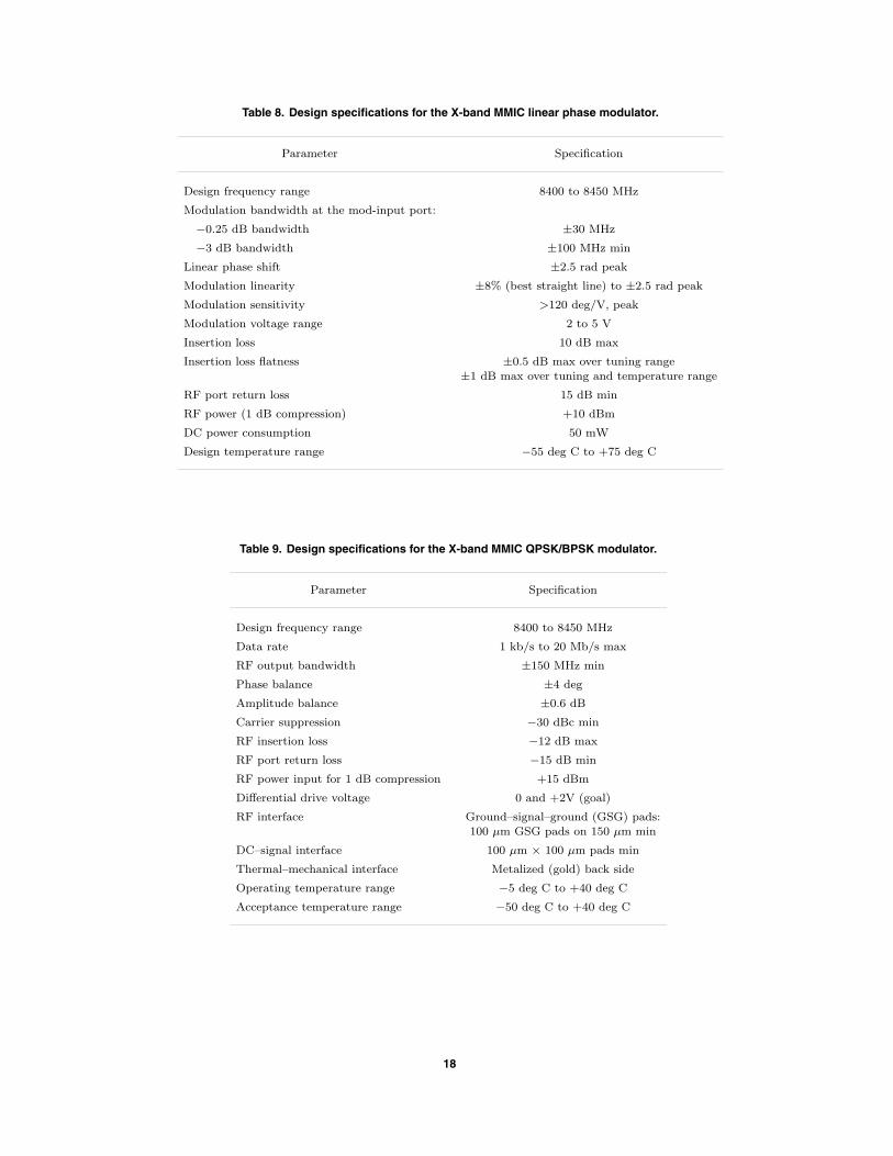
Table 8. Design specifications for the X-band MMIC linear phase modulator.
Parameter Specification
Design frequency range 8400 to 8450 MHz
Modulation bandwidth at the mod-input port:
−0.25 dB bandwidth ±30 MHz
−3 dB bandwidth ±100 MHz min
Linear phase shift ±2.5 rad peak
Modulation linearity ±8% (best straight line) to ±2.5 rad peak
Modulation sensitivity >120 deg/V, peak
Modulation voltage range 2 to 5 V
Insertion loss 10 dB max
Insertion loss flatness ±0.5 dB max over tuning range±1 dB max over tuning and temperature range
RF port return loss 15 dB min
RF power (1 dB compression) +10 dBm
DC power consumption 50 mW
Design temperature range −55 deg C to +75 deg C
Table 9. Design specifications for the X-band MMIC QPSK/BPSK modulator.
Parameter Specification
Design frequency range 8400 to 8450 MHz
Data rate 1 kb/s to 20 Mb/s max
RF output bandwidth ±150 MHz min
Phase balance ±4 deg
Amplitude balance ±0.6 dB
Carrier suppression −30 dBc min
RF insertion loss −12 dB max
RF port return loss −15 dB min
RF power input for 1 dB compression +15 dBm
Differential drive voltage 0 and +2V (goal)
RF interface Ground–signal–ground (GSG) pads:100 µm GSG pads on 150 µm min
DC–signal interface 100 µm × 100 µm pads min
Thermal–mechanical interface Metalized (gold) back side
Operating temperature range −5 deg C to +40 deg C
Acceptance temperature range −50 deg C to +40 deg C
18

B. Ka-Band Receiver and Transmitter Microwave Components
The specifications for the Ka-band components, including the pre-select filter, LNA, multi-channelKa-Band DRO, linear phase modulator, and QPSK modulator, are given in Tables 10 through 14.
1. LNA. Ka-band LNA MMICs with a 2-dB noise figure and a 15-dB gain are commercially available.
2. Linear Modulator and Phase Shifter. Voltage-controlled active phase shifting will be usedto design linear phase modulators and phase shifters. The present technology utilizes a Ka-band MMICvaractor-based design to provide the linear phase shifting function. The Ka-band MMIC phase shifter,QPSK modulator, and x4 multiplier are currently under development at the Applied Physics Laboratory(APL) for JPL/NASA. The MMICs chips to be developed represent the core Ka-band chips needed forthe next generation of advanced transponders.
The desired functional specification for the Ka-band MMIC phase shifter is shown in Table 13. Themain specification goal is to provide a phase shift of ±2.5 rad with linearity better than ±8 percent withlow amplitude insertion loss variation of ±0.5 dB over the tuning range. The phase shifter also is used inthe phased array application.
The main objective of the QPSK modulator is to provide the 1-kb/s to 100-Mb/s data-rate capabilityfuture Mars and other space missions require to transmit science data and video signals to Earth. Adigital binary phase-shift keying (BPSK)/QPSK modulator at Ka-band is preferred over X-band becauseof channel bandwidth constraints and performance limitations at X-band.
Table 10. Multi-channel receiver/transmitter Ka-DRO specification.
DRO parameter Specification
X-band RF frequency range:
X-band receive DRO frequency range ∼34 GHz (TBD)
X-band transmit DRO frequency range ∼32 GHz (TBD)
Course electronic tuning range (receiver) TBD: ∼34 MHz ± 100 MHz
Fine tuning range (PLL capture range) ±2 MHz
Tuning linearity ±10% or better
Output power level +10 dBm ± 1.0 dB
Free-running DRO SSB phase noise < −50 dBc/Hz at 1 kHz off carrier
Frequency stability versus temperature ±2 ppm/deg C max
Frequency pushing (±5% Vdc) 100 kHz max
Frequency pulling (2:1 VSWR all phases) 200 kHz max
Harmonics < −33 dBc
Spurious signals < −80 dBc
Operating temperature range −55 deg C to +75 deg C
Output impedance 50 ± 5 ohms, nominal
DC bias current at +5V DC 100 mA
Course electronic tuning control voltage +3 V ± 2 V max
Fine tuning control voltage +3V ± 2 V max
19
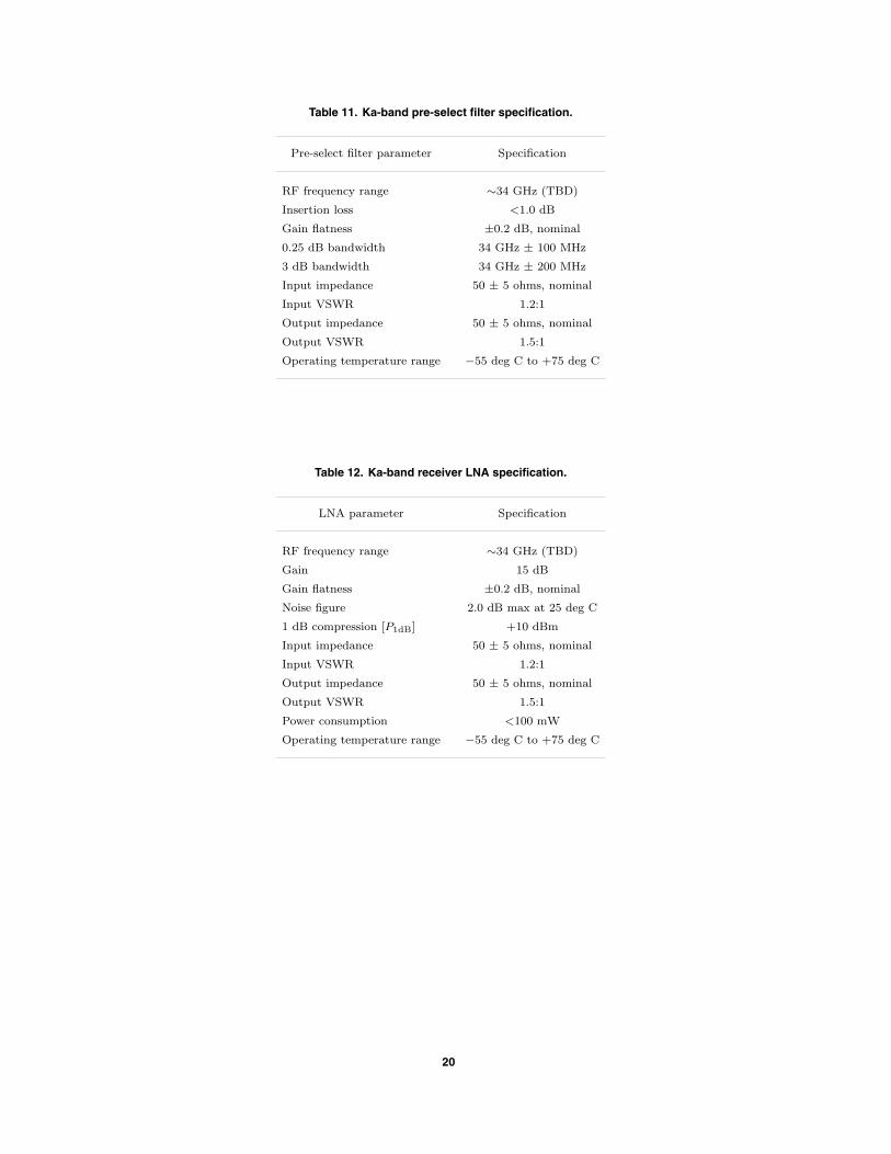
Table 11. Ka-band pre-select filter specification.
Pre-select filter parameter Specification
RF frequency range ∼34 GHz (TBD)
Insertion loss <1.0 dB
Gain flatness ±0.2 dB, nominal
0.25 dB bandwidth 34 GHz ± 100 MHz
3 dB bandwidth 34 GHz ± 200 MHz
Input impedance 50 ± 5 ohms, nominal
Input VSWR 1.2:1
Output impedance 50 ± 5 ohms, nominal
Output VSWR 1.5:1
Operating temperature range −55 deg C to +75 deg C
Table 12. Ka-band receiver LNA specification.
LNA parameter Specification
RF frequency range ∼34 GHz (TBD)
Gain 15 dB
Gain flatness ±0.2 dB, nominal
Noise figure 2.0 dB max at 25 deg C
1 dB compression [P1dB] +10 dBm
Input impedance 50 ± 5 ohms, nominal
Input VSWR 1.2:1
Output impedance 50 ± 5 ohms, nominal
Output VSWR 1.5:1
Power consumption <100 mW
Operating temperature range −55 deg C to +75 deg C
20
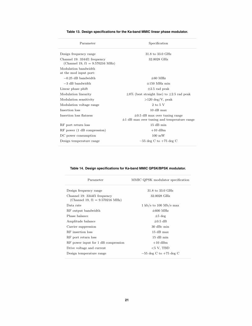
Table 13. Design specifications for the Ka-band MMIC linear phase modulator.
Parameter Specification
Design frequency range 31.8 to 33.0 GHz
Channel 19: 3344f1 frequency 32.0028 GHz(Channel 19, f1 = 9.570216 MHz)
Modulation bandwidthat the mod input port:
−0.25 dB bandwidth ±60 MHz
−3 dB bandwidth ±150 MHz min
Linear phase phift ±2.5 rad peak
Modulation linearity ±8% (best straight line) to ±2.5 rad peak
Modulation sensitivity >120 deg/V, peak
Modulation voltage range 2 to 5 V
Insertion loss 10 dB max
Insertion loss flatness ±0.5 dB max over tuning range±1 dB max over tuning and temperature range
RF port return loss 15 dB min
RF power (1 dB compression) +10 dBm
DC power consumption 100 mW
Design temperature range −55 deg C to +75 deg C
Table 14. Design specifications for Ka-band MMIC QPSK/BPSK modulator.
Parameter MMIC QPSK modulator specification
Design frequency range 31.8 to 33.0 GHz
Channel 19: 3344f1 frequency 32.0028 GHz(Channel 19, f1 = 9.570216 MHz)
Data rate 1 kb/s to 100 Mb/s max
RF output bandwidth ±600 MHz
Phase balance ±5 deg
Amplitude balance ±0.5 dB
Carrier suppression 30 dBc min
RF insertion loss 15 dB max
RF port return loss 15 dB min
RF power input for 1 dB compression +10 dBm
Drive voltage and current <5 V, TBD
Design temperature range −55 deg C to +75 deg C
21

C. S-Band Components
The required S-band RF components are commercially available, and no new development is necessaryat this time.
D. Future Technology Developments
The following tasks represent development work still to be completed. With the exception of thefirst task, the X-band DRO development, these developments are not funded by the current researchand development technology effort but are being pursued under other technology and flight hardwaredevelopment programs.
(1) Complete the development of the X-band multi-channel DRO.
(2) Develop the Ka-band multi-channel DRO to cover Ka-band channels.
(3) Develop micro-miniature low-loss pre-select filters for S-band, X-band, and Ka-band receiverapplications using high-Q dielectric resonator-based circuits.
(4) Develop micro-electro-mechanical (MEM) switches for X-band and Ka-band applications.
(5) Evaluate the S-band direct vector modulator for linear phase modulation, and BPSK/QPSK,and phased-array applications.
(6) Develop X-band and Ka-band vector modulators.
(7) Evaluate ferroelectric thin-film phase shifters and varactors. A novel phase-shifter technol-ogy developed under Defense Advanced Research Projects Agency (DARPA) utilizes ferro-electric thin-film technology to provide voltage-tunable X-band and Ka-band phase shifterswith large linear tuning range. The tunable circuit products based on the ferroelectricbarium strontium titanate (BST) are still under development and expected to be availablewithin a year. We will continue to assess and evaluate these technologies and products forthe advanced transponder and phased array and other space applications.
(8) Evaluate pseudomorphic high electron mobility transistor (P-HEMT) technology and het-erojunction bipolar transistor (HBT) technology applicability for low-noise and high-powerapplications at X-band and Ka-band.
(9) Study the applicability of silicon–germanium (SiGe) RFIC technology to highly inte-grated, micro-miniature, low-power X-band transponder and ultra-high frequency (UHF)transceivers for Mars and other space applications. A four-chip architecture and solutionwill be attempted. The receiver, phase-locked-loop synthesizer, transmitter, and modulatorfunctions will be included in the RF multi-chip configuration. Future spacecraft such asmicro-satellites and Mars rovers for space exploration require micro-miniaturized commu-nication systems with low power, low mass, and versatile communication systems. SiGeprovides a high level of integration at low voltage and low power operation at low costpotential.
V. Digital Design Specifications and Analysis
A. Carrier-Tracking Loop Architecture
This section discusses the requirements and architectural trade-offs involved in the design of the carrier-tracking loop for the Advanced Transponder.
22
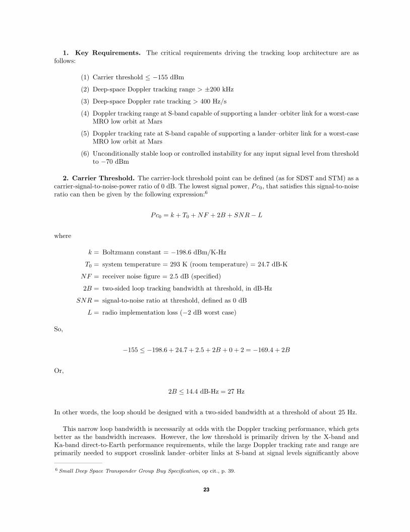
1. Key Requirements. The critical requirements driving the tracking loop architecture are asfollows:
(1) Carrier threshold ≤ −155 dBm
(2) Deep-space Doppler tracking range > ±200 kHz
(3) Deep-space Doppler rate tracking > 400 Hz/s
(4) Doppler tracking range at S-band capable of supporting a lander–orbiter link for a worst-caseMRO low orbit at Mars
(5) Doppler tracking rate at S-band capable of supporting a lander–orbiter link for a worst-caseMRO low orbit at Mars
(6) Unconditionally stable loop or controlled instability for any input signal level from thresholdto −70 dBm
2. Carrier Threshold. The carrier-lock threshold point can be defined (as for SDST and STM) as acarrier-signal-to-noise-power ratio of 0 dB. The lowest signal power, Pc0, that satisfies this signal-to-noiseratio can then be given by the following expression:6
Pc0 = k + T0 + NF + 2B + SNR − L
where
k = Boltzmann constant = −198.6 dBm/K-Hz
T0 = system temperature = 293 K (room temperature) = 24.7 dB-K
NF = receiver noise figure = 2.5 dB (specified)
2B = two-sided loop tracking bandwidth at threshold, in dB-Hz
SNR = signal-to-noise ratio at threshold, defined as 0 dB
L = radio implementation loss (−2 dB worst case)
So,
−155 ≤ −198.6 + 24.7 + 2.5 + 2B + 0 + 2 = −169.4 + 2B
Or,
2B ≤ 14.4 dB-Hz = 27 Hz
In other words, the loop should be designed with a two-sided bandwidth at a threshold of about 25 Hz.
This narrow loop bandwidth is necessarily at odds with the Doppler tracking performance, which getsbetter as the bandwidth increases. However, the low threshold is primarily driven by the X-band andKa-band direct-to-Earth performance requirements, while the large Doppler tracking rate and range areprimarily needed to support crosslink lander–orbiter links at S-band at signal levels significantly above
6 Small Deep Space Transponder Group Buy Specification, op cit., p. 39.
23
threshold. Here, we are aided by the automatic gain control (AGC) function preceding the carrier-tracking loop. The loop gain, and therefore the bandwidth, depends on the power level of the inputsignal. The AGC function serves to normalize the input signal level by the detected total power andtherefore maintains a constant loop input power level, as long as the signal power is significantly greaterthan the noise power. As the signal power drops to the point where the noise contribution is significant,normalizing the input signal by the total detected power begins to reduce the actual signal strength andgain of the tracking loop. This in turn causes the bandwidth to contract for weak signals, which bothenhances the detection threshold and reduces the tracking range. In the design of the STM AGC andtracking loop, a bandwidth compression factor of about 10 was obtained in going from strong signal tothreshold. With a similar design, then, we expect to see a loop bandwidth of 200 to 250 Hz at strongsignal.
3. Carrier Tracking. For standard second-order-loop damping in the range of 0.5 to 1, the naturalfrequency of the loop, ωn, is roughly equal to the one-sided loop bandwidth. The Doppler tracking rangeof the loop then can be estimated by requiring that the acceleration error, ∆(dω/dτ)/ω2
n, be maintainedreasonably small, or less than about 30 deg or so for reliable tracking [5]. For a ωn of about 125 Hz then,we should be able to track a Doppler rate of about (30/360) ∗ 125 Hz2 = 1300 Hz/s.
The total Doppler tracking range can similarly be estimated by requiring that the residual trackingphase error be kept small. A second-order loop will track out a static frequency offset, but deviationfrom the ideal infinite-gain integrator will cause leakage resulting in a static phase error, given by thefrequency offset divided by the loop gain: 2π∆f/K. For total gain values of a few times 107, as achievedfor STM, this results in a phase error of about 1 deg for an offset of 100 kHz. This implies that Doppleroffsets of up to 1 MHz can be supported with a relatively small phase error. However, as the gain dropsoff at lower signal levels, this tracking range will shrink, and for signal levels about 10 dB above thresholdand higher, we can expect to be able to track about ±500 kHz of static Doppler.
As seen from the requirements above, this performance is sufficient to meet the requirements fordeep-space acquisition and tracking at X-band, but what about for proximity links at S-band?
As a way to bound the proximity Doppler requirements, we considered the worst-case low orbit ofthe planned Mars Reconnaissance Orbiter (MRO) (which will use a UHF proximity link). Trajectorysimulator models for an MRO orbit at 200 km show7 a peak Doppler rate of 90 Hz/s on a 400-MHz UHFcarrier, and a total Doppler range during a pass of −5 kHz to +5 kHz. Since we plan to use S-band, at2.1 GHz for proximity links with the Advanced Transponder, we need to scale these modeled numbers upby a factor of five to get proximity Doppler tracking rate and range requirements at S-band of 450 Hz/sfor the rate and ±25 kHz for the range for a worst-case low-orbit pass.
The second-order loop parameters above would suggest that both the deep-space and proximityDoppler tracking rate and range requirements can be met with a second-order loop similar to that plannedfor STM. In addition, the second-order loop has the advantage of being simpler to analyze and, mostimportantly, of being unconditionally stable at all input signal levels and phases. For these reasons, wewill implement the Advanced Transponder carrier-tracking loop as a second-order phase-locked loop.
In addition, because the tracking loop is closed digitally, we will be able to reprogram the tracking-loop filter parameters on the fly. This will allow us to expand the loop bandwidth and improve thetracking performance at the expense of signal threshold. For example, a factor of two expansion ofthe loop bandwidth will degrade the threshold by 3 dB, but provide a factor of four improvement inDoppler tracking rate. Since most proximity links will operate at strong signal levels, we can use thisprogrammability to our advantage to optimize the tracking loop for the required application.
7 D. J. Bell, personal communication, MRO Telecom Systems Engineer, Jet Propulsion Laboratory, Pasadena, California,April 2003.
24
B. High-Rate Command Detector
In addition to the standard command detection unit (CDU), we also will provide a high-rate commanddetector (HRCD) in order to enhance the uplink command rate to 256 kb/s or more, compared to theSDST and STM maximum rates of 2 kb/s. The HRCD will demodulate PSK-modulated data from theuplink carrier. This section provides a description of the HRCD architecture and analysis.
The core of the HRCD is a straightforward integrate-and-dump detector with a digital phase-trackingloop. In the case of the transponder, we know that the bit rate is exactly synchronous with the masterclock, since the master clock is adjusted to track the received carrier. This simplifies the design problem,as we have only one variable to track, the bit timing, as opposed to the traditional PLL bit detectorwhere both frequency and phase must be recovered and tracked.
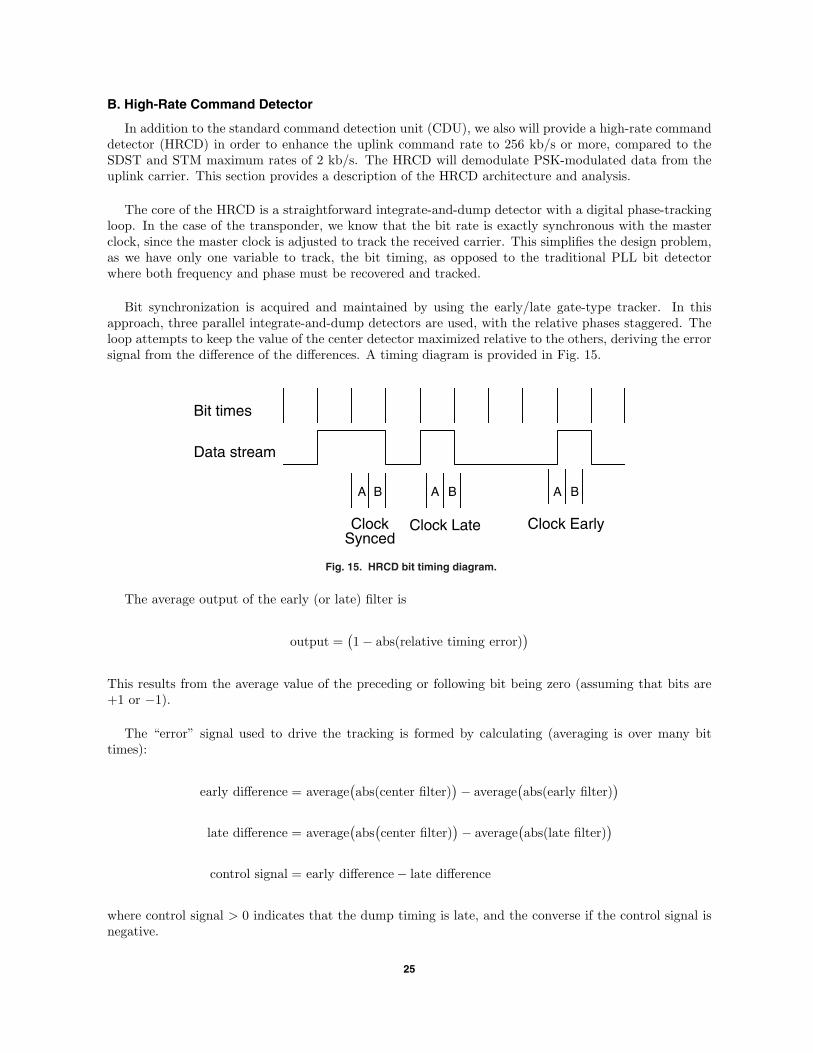
Bit synchronization is acquired and maintained by using the early/late gate-type tracker. In thisapproach, three parallel integrate-and-dump detectors are used, with the relative phases staggered. Theloop attempts to keep the value of the center detector maximized relative to the others, deriving the errorsignal from the difference of the differences. A timing diagram is provided in Fig. 15.
A B
Clock Late Clock EarlyClockSynced
Bit times
Data stream
A B A B
Fig. 15. HRCD bit timing diagram.
The average output of the early (or late) filter is
output =(1 − abs(relative timing error)
)
This results from the average value of the preceding or following bit being zero (assuming that bits are+1 or −1).
The “error” signal used to drive the tracking is formed by calculating (averaging is over many bittimes):
early difference = average(abs(center filter)
)− average
(abs(early filter)
)
late difference = average(abs
(center filter)
)− average
(abs(late filter)
)
control signal = early difference − late difference
where control signal > 0 indicates that the dump timing is late, and the converse if the control signal isnegative.
25
In a practical implementation of this approach, the integration is done in two stages. First, the inputsamples are accumulated in a high-rate integrate and dump, with samples “dumped” at a convenient rate,typically 16 or 32 times the bit rate. The 16× bit-rate samples then are summed to produce the finaloutput. Design trade-offs can be made to select the precision and number of stages for each integrateand dump to optimize power dissipation (the lower-frequency stages clock at slower rates and consumeless power). A block diagram of the HRCD is shown in Fig. 16.
In our implementation, the outputs of the three detectors (after averaging) are compared and usedto determine whether to add or drop a clock pulse from the counter that determines the timing of theintegrators. This moves the filter timing one step later or earlier.
The tracking-loop performance is a combination of the amount of early/late timing stagger, the lengthof time over which the filter outputs are averaged, the frequency of clock adjustments, and the size of theclock step. The highly non-linear nature of the entire tracking and detection process makes simulationthe preferred means to evaluate changes in the design parameters. Sample bit streams can be createdwith varying noise and bandwidth characteristics and processed through the tracking algorithm, withactual bit-error rate (BER) measurements made.
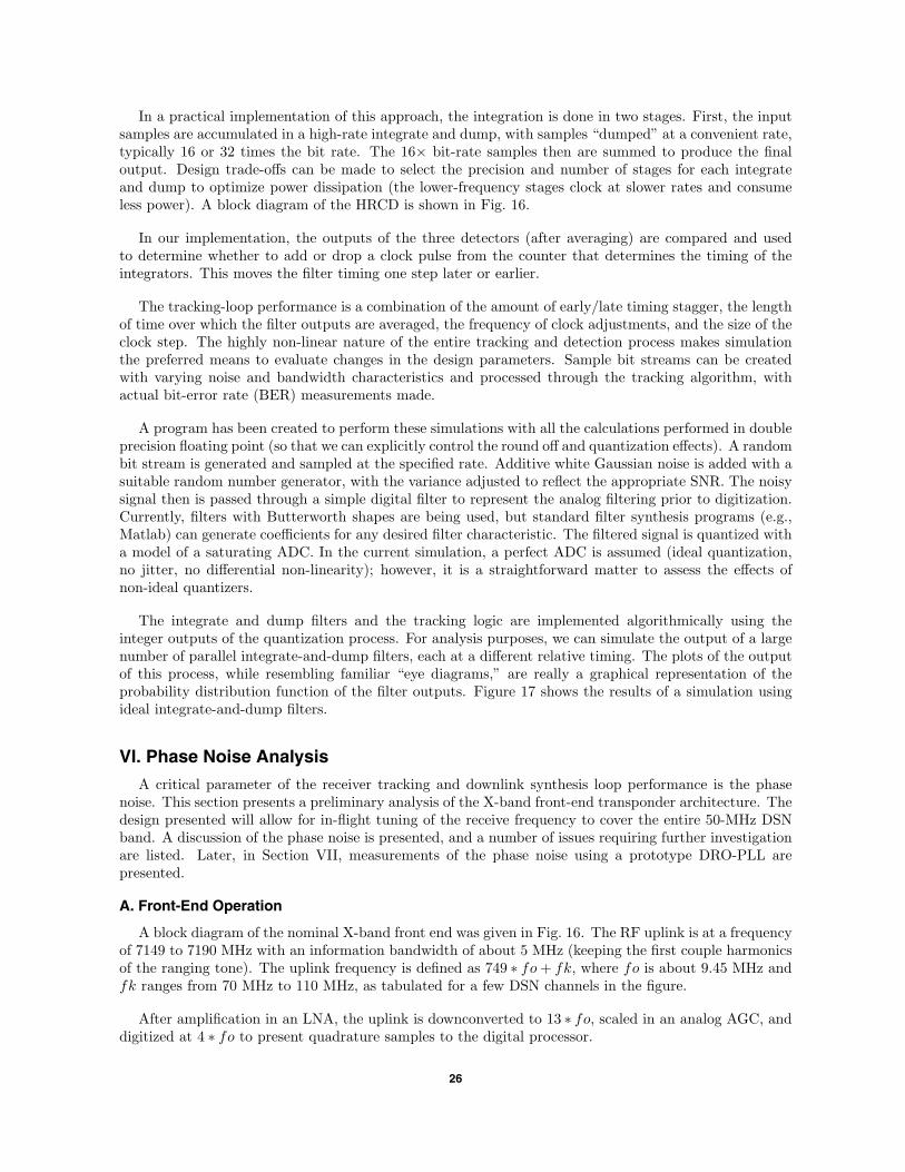
A program has been created to perform these simulations with all the calculations performed in doubleprecision floating point (so that we can explicitly control the round off and quantization effects). A randombit stream is generated and sampled at the specified rate. Additive white Gaussian noise is added with asuitable random number generator, with the variance adjusted to reflect the appropriate SNR. The noisysignal then is passed through a simple digital filter to represent the analog filtering prior to digitization.Currently, filters with Butterworth shapes are being used, but standard filter synthesis programs (e.g.,Matlab) can generate coefficients for any desired filter characteristic. The filtered signal is quantized witha model of a saturating ADC. In the current simulation, a perfect ADC is assumed (ideal quantization,no jitter, no differential non-linearity); however, it is a straightforward matter to assess the effects ofnon-ideal quantizers.
The integrate and dump filters and the tracking logic are implemented algorithmically using theinteger outputs of the quantization process. For analysis purposes, we can simulate the output of a largenumber of parallel integrate-and-dump filters, each at a different relative timing. The plots of the outputof this process, while resembling familiar “eye diagrams,” are really a graphical representation of theprobability distribution function of the filter outputs. Figure 17 shows the results of a simulation usingideal integrate-and-dump filters.
VI. Phase Noise Analysis
A critical parameter of the receiver tracking and downlink synthesis loop performance is the phasenoise. This section presents a preliminary analysis of the X-band front-end transponder architecture. Thedesign presented will allow for in-flight tuning of the receive frequency to cover the entire 50-MHz DSNband. A discussion of the phase noise is presented, and a number of issues requiring further investigationare listed. Later, in Section VII, measurements of the phase noise using a prototype DRO-PLL arepresented.
A. Front-End Operation
A block diagram of the nominal X-band front end was given in Fig. 16. The RF uplink is at a frequencyof 7149 to 7190 MHz with an information bandwidth of about 5 MHz (keeping the first couple harmonicsof the ranging tone). The uplink frequency is defined as 749 ∗ fo + fk, where fo is about 9.45 MHz andfk ranges from 70 MHz to 110 MHz, as tabulated for a few DSN channels in the figure.
After amplification in an LNA, the uplink is downconverted to 13 ∗ fo, scaled in an analog AGC, anddigitized at 4 ∗ fo to present quadrature samples to the digital processor.
26
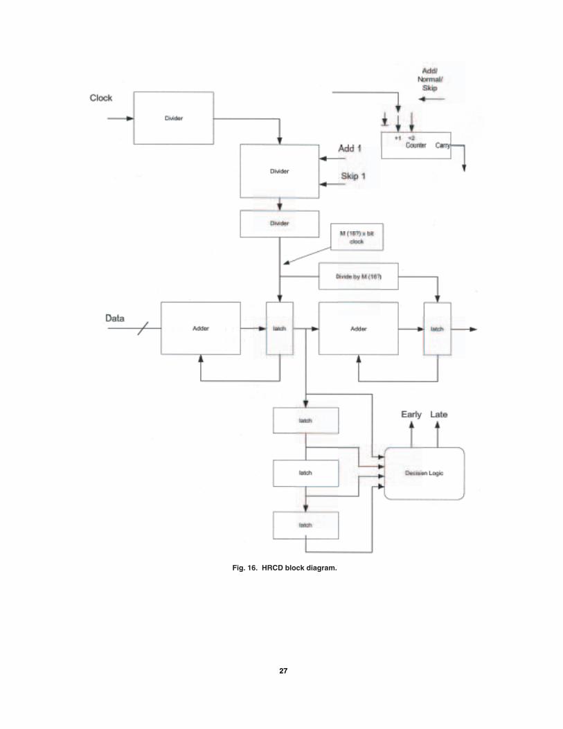
Fig. 16. HRCD block diagram.
27

Bit times
Data stream
IdealizedIntegrate and
Dump
Early
On-Time
Late
Fig. 17. Ideal integrate-and-dump operation of HRCD.
The downconversion is accomplished using a DRO-PLL. The DRO operates at a frequency of 736 ∗fo+fk and is tunable over the 50-MHz range of fk by applying a DC bias derived from a bias DAC thatis digitally programmable. The ability to pull the DRO frequency over this range was demonstrated inthe laboratory; see Section VII. Using a new DRO design, we were able to increase the DRO tuning rangefrom the ∼10-MHz STM design to >50 MHz. The DRO output is mixed down to DC using a samplingphase detector (SPD). The SPD step-recovery diode is driven by the upper sideband produced by mixingthe reference oscillator (∼151 MHz) and a digitally synthesized fk/46 sine wave (∼1.5 to 2.5 MHz). Notethat the bandpass filter after this mixer must pass the upper sideband (∼151.5 to 152.5 MHz) but rejectthe lower sideband (∼149.5 to 148.5 MHz). A selection criterion for the fo and fk combination will bethe ease of constructing this filter; larger values of fk will simplify the filter and increase the spacing ofleak-through harmonics in the PLL but will also reduce the oversampling factor of the receiver NCO/DACand degrade the phase noise. Work done in the laboratory suggests that about 10 MHz may be a betterchoice for fk.
The sampling phase detector will sample the DRO with the 46th harmonic of the (oscillator) ×(receiver NCO) signal, producing a phase-error signal that will be filtered and combined with the overall
28
DC bias voltage to control the DRO frequency. This error signal will be applied to the lightly coupledvaractor port of the DRO. The tightly coupled port will be used for quasi-static channel-selection tuningusing a bias DAC. An issue that must be investigated is how much noise pickup can be tolerated onthe bias DAC output. By design, the DRO frequency will be very sensitive to voltage variations on thissignal, and any noise will cause frequency modulation that will appear on the 13fo IF carrier. However,the bias DAC signal can be filtered with a very long time constant if necessary, as there is no operationalrequirement to rapidly switch DSN frequency.
1. Loop Phase Noise. Phase noise on the DRO will appear on the 13 fo IF and degrade thenavigation and communications performance of the transponder.
The main architectural difference between this design and that used in STM is that here the refer-ence oscillator is mixed with the receiver NCO frequency before “multiplication” in the sampling phasedetector. In the STM design,8 the reference oscillator is used to sample the DRO, and the resulting IF(around 8 MHz) then is mixed with the receiver NCO output. If the phase noise of the NCO is largerthan that of the reference oscillator, then the current design clearly will be limited by the NCO since itsphase noise will be multiplied up in the SPD. Theoretically, however, the phase noise of the NCO outputshould be lower than that of the reference oscillator by 20 ∗ log(2 MHz/150 MHz), or −43.5 dB, sincethe NCO is referenced to the reference oscillator. However, the DAC itself contributes a certain noisefloor due to random thermal effects, etc., which prevents the lower bound from actually being reached.So, the requirement for this design is that the intrinsic noise floor of the DAC (and to some extent theupstream electronics) not exceed the phase noise due to the reference oscillator. If this condition is met,this architecture actually will produce an improvement of 6 dB over the STM design since the referenceis multiplied by 46 instead of 92 due to the reference frequency going from 8 ∗ fo to 16 ∗ fo. (Of course,the 152-MHz oscillator may have 6-dB worse phase noise performance than the 76-MHz oscillator if theyboth are derived by multiplication of a lower-frequency crystal reference).
To look at some sample numbers, a very good low-noise crystal oscillator in the 100-MHz range mayhave a phase noise performance of around −155 dBc/Hz at 1 kHz, flattening to −160 dBc/Hz at 10 kHz[6] (although note that the Deep Space Transponder (DST) specification sets the input phase noise ofthe ultra-stable oscillator (USO) at only −125 dBc/Hz at 10 kHz—significantly worse performance).As this reference is multiplied up in the SPD by a factor of 46, the phase noise will degrade to about−160 + 20 ∗ log(46) = −126 dBc/Hz at 10 kHz.
Theoretically, phase noise of the NCO output would be improved by −43 dB over the reference oscillatorit is locked to, or about −200 dBc/Hz. However, the noise floor of the DAC component will limit thisimprovement. Noise floors typically are better than −165 dBc/Hz for transistor–transistor logic (TTL)parts, to −150 dBc/Hz for emitter-coupled logic (ECL) parts, and some PLL ICs have noise floors ashigh as −130 dBc/Hz.9 For parts at −165 dBc/Hz, the NCO noise will not significantly degrade thereference oscillator noise, and the reference oscillator will dominate the loop performance. For an ECL-type part at −150 dBc/Hz, the NCO will be the dominant contribution, and the overall phase noise ofthe loop, after the factor 46 multiplication, will be about −110 dBc/Hz at 10 kHz. By contrast, the STMarchitecture would hide the noise floor performance of this part because it would enter the loop after the×92 multiplication, and the overall loop would run at −126 dBc/Hz for the oscillator performance givenabove.
What sort of performance do we need? The most relevant specification is the phase noise performancerequired of the downlink carrier, operating in coherent mode. In this mode, the phase noise will be due tothe combination of the uplink DRO loop phase noise entering the IF and the downlink DRO loop phase
8 S. Kayalar, “STM 736 fo DRO PLL Design,” JPL Interoffice Memorandum 3366-00-015 (internal document), Jet Propul-sion Laboratory, Pasadena, California, May 5, 2000.
9 EMF Systems, Inc., State College, Pennsylvania.
29

noise (which will be nearly identical in design). The Deep Space Transponder specifies that the phasenoise power spectral density on the downlink in this mode be below −93 dBc/Hz at a 10-kHz offset fromthe carrier and below −125 dBc/Hz at a 25-MHz offset from the carrier. Assuming that the receiverand synthesizer DRO loops contribute equally, we would conclude that the performance should be betterthan about −96 dBc/Hz at 10 kHz. This would suggest that even with some noise-floor degradation dueto the DAC, we can still meet this requirement. Note that the wideband performance requirement of−125 dBc/Hz at 25 MHz will really be placed on the DRO. This is beyond the PLL loop bandwidth and,therefore, will not be affected by the loop architecture. A typical X-band DRO should be able to achievearound −140 dBc/Hz or better at deviations beyond 1 MHz.
2. Open Issues. There remain a number of open issues to be worked. Some are listed below:
(1) The DRO frequency tuning range must be investigated—preliminary laboratory work hasdemonstrated a >50-MHz tuning range.
(2) Noise power levels on the bias DAC must be investigated and a maximum FM noise on theDRO specified.
(3) The choice of fo and fk should be optimized.
(4) The noise floor of the DAC and associated components must be investigated in more de-tail. Preliminary laboratory work with the NCO shows promise, but spurious noise in the100-kHz range due to internal FPGA switching noise currently is limiting the measurements.Follow-on work employing Schmidt-trigger buffers should mitigate this problem.
VII. Experimental Results
In order to establish the feasibility of our architecture, we developed breadboard hardware in the labo-ratory using residual hardware from the STM development when available and designing new componentswhen required.
A. X-Band DRO with Dual Varactors
A key aspect of the Advanced Transponder architecture is the ability to tune the frequency of thereceiver and transmitter dielectric resonance oscillators (DROs) in order to cover the entire DSN band.To demonstrate this principle, we designed and fabricated a dual-varactor DRO substrate and populatedit with a voltage-controlled oscillator (VCO) MMIC, two varactor diodes, and a dielectric puck from STMresidual stock. Figure 18 is a photograph of one of the X-band DROs we fabricated for this effort.
In this DRO design, the loosely coupled varactor, pictured above the dielectric puck in Fig. 18, isused for fine tuning of the DRO frequency and is the control port used to close the phase-locked loop.The tightly coupled varactor is shown to the left of the puck and is designed to be driven by the outputof a coarse frequency control, or channel-select digital-to-analog converter (DAC). This DAC output isheavily low-pass filtered and is designed to hold a quasi-static tuning voltage for DSN frequency channelselection. The DROs designed for the STM development were designed to have a tuning range of about10 MHz. For this development, we went to two varactors in order to achieve a tuning range greaterthan the DSN allocation bandwidth of 50 MHz at X-band in order to provide in-flight channel selection.Laboratory measurements of our prototype design have demonstrated that tuning ranges of greater than60 MHz are possible, as shown in Fig. 19.
In order to demonstrate the operation of the DRO in the relevant phase-locked loop environment, weused an Alpha sampling phase detector from STM residual stock to put together a simple first-order loopto phase lock the DRO to a frequency reference provided by an HP 8663 synthesized frequency generator.A block diagram of the laboratory setup is shown in Fig. 20.
30
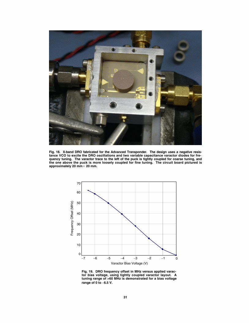
Fig. 18. X-band DRO fabricated for the Advanced Transponder. The design uses a negative resis-tance VCO to excite the DRO oscillations and two variable capacitance varactor diodes for fre-quency tuning. The varactor trace to the left of the puck is tightly coupled for coarse tuning, andthe one above the puck is more loosely coupled for fine tuning. The circuit board pictured isapproximately 20 mm 20 mm.
60
50
40
30
20
10
0−7 −6 −5 −4 −3 −2 −1 0
Varactor Bias Voltage (V)
70
Fre
quen
cy O
ffset
(M
Hz)
Fig. 19. DRO frequency offset in MHz versus applied varac-tor bias voltage, using tightly coupled varactor layout. Atuning range of >60 MHz is demonstrated for a bias voltagerange of 0 to −6.5 V.
31
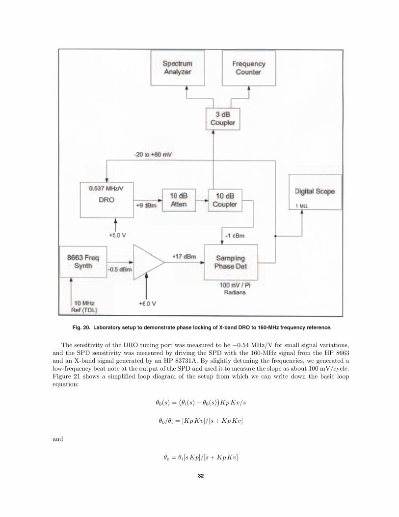
Fig. 20. Laboratory setup to demonstrate phase locking of X-band DRO to 160-MHz frequency reference.
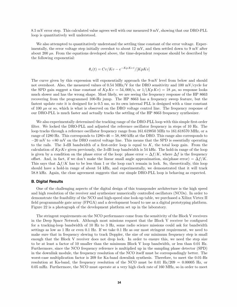
The sensitivity of the DRO tuning port was measured to be −0.54 MHz/V for small signal variations,and the SPD sensitivity was measured by driving the SPD with the 160-MHz signal from the HP 8663and an X-band signal generated by an HP 83731A. By slightly detuning the frequencies, we generated alow-frequency beat note at the output of the SPD and used it to measure the slope as about 100 mV/cycle.Figure 21 shows a simplified loop diagram of the setup from which we can write down the basic loopequation:
θ0(s) =(θi(s) − θ0(s)
)Kp Kv/s
θ0/θi = [Kp Kv]/[s + Kp Kv]
and
θe = θi[s Kp]/[s + Kp Kv]
32
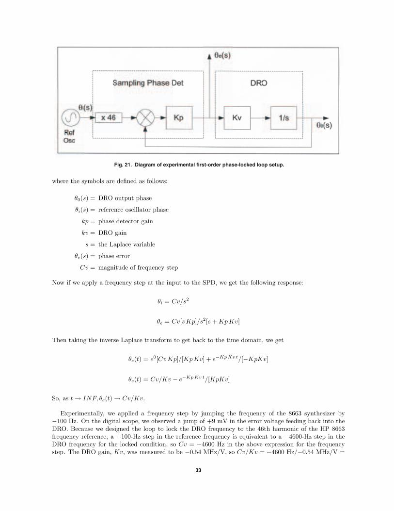
Fig. 21. Diagram of experimental first-order phase-locked loop setup.
where the symbols are defined as follows:
θ0(s) = DRO output phase
θi(s) = reference oscillator phase
kp = phase detector gain
kv = DRO gain
s = the Laplace variable
θe(s) = phase error
Cv = magnitude of frequency step
Now if we apply a frequency step at the input to the SPD, we get the following response:
θi = Cv/s2
θe = Cv[s Kp]/s2[s + Kp Kv]
Then taking the inverse Laplace transform to get back to the time domain, we get
θe(t) = e0[Cv Kp]/[Kp Kv] + e−Kp Kv t/[−KpKv]
θe(t) = Cv/Kv − e−Kp Kv t/[KpKv]
So, as t → INF, θe(t) → Cv/Kv.
Experimentally, we applied a frequency step by jumping the frequency of the 8663 synthesizer by−100 Hz. On the digital scope, we observed a jump of +9 mV in the error voltage feeding back into theDRO. Because we designed the loop to lock the DRO frequency to the 46th harmonic of the HP 8663frequency reference, a −100-Hz step in the reference frequency is equivalent to a −4600-Hz step in theDRO frequency for the locked condition, so Cv = −4600 Hz in the above expression for the frequencystep. The DRO gain, Kv, was measured to be −0.54 MHz/V, so Cv/Kv = −4600 Hz/−0.54 MHz/V =
33
8.5 mV error step. This calculated value agrees well with our measured 9 mV, showing that our DRO-PLLloop is quantitatively well understood.
We also attempted to quantitatively understand the settling time constant of the error voltage. Exper-imentally, the error voltage step initially overshot to about 12 mV, and then settled down to 9 mV afterabout 200 µs. From the equations developed above, the time-dependent response should be described bythe following exponential:
θe(t) = Cv/Kv − e−Kp Kv t/[KpKv]
The curve given by this expression will exponentially approach the 9-mV level from below and shouldnot overshoot. Also, the measured values of 0.54 MHz/V for the DRO sensitivity and 100 mV/cycle forthe SPD gain suggest a time constant of Kp Kv = 54, 000/s, or 1/(Kp Kv) = 18 µs, so response looksmuch slower and has the wrong shape. Most likely, we are seeing the frequency response of the HP 8663recovering from the programmed 100-Hz jump. The HP 8663 has a frequency sweep feature, but thefastest update rate it is designed for is 0.5 ms, so its own internal PLL is designed with a time constantof 100 µs or so, which is what is observed on the DRO voltage control line. The frequency response ofour DRO-PLL is much faster and actually tracks the settling of the HP 8663 frequency synthesizer.
We also experimentally determined the tracking range of the DRO-PLL loop with this simple first-orderfilter. We locked the DRO-PLL and adjusted the reference oscillator frequency in steps of 10 Hz. Theloop tracks through a reference oscillator frequency range from 161.619850 MHz to 161.618570 MHz, or arange of 1280 Hz. This corresponds to 1280∗46 = 58, 880 kHz at the DRO. This range also corresponds to−20 mV to +80 mV on the DRO control voltage line. This means that the SPD is essentially operatingto the rails. The 3-dB bandwidth of a first-order loop is equal to K, the total loop gain. From thecalculation of Kp Kv given previously, the 3-dB loop bandwidth is 54 kHz. The hold-in range of the loopis given by a condition on the phase error of the loop: phase error = ∆f/K, where ∆f is the frequencyoffset. And, in fact, if we don’t make the linear small angle approximation, sin(phase error) = ∆f/K.This says that ∆f/K has to be less than 1 or the loop can’t remain in lock. So, theoretically, this loopshould have a hold-in range of about 54 kHz, and experimentally, we demonstrated that it will track58.8 kHz. Again, the close agreement suggests that our simple DRO-PLL loop is behaving as expected.
B. Digital Results
One of the challenging aspects of the digital design of this transponder architecture is the high speedand high resolution of the receiver and synthesizer numerically controlled oscillators (NCOs). In order todemonstrate the feasibility of the NCO and high-speed sine look-up table, we purchased a Xilinx Virtex IIfield programmable gate array (FPGA) and a development board to use as a digital prototyping platform.Figure 22 is a photograph of the development platform set up in the laboratory.
The stringent requirements on the NCO performance come from the sensitivity of the Block V receiversin the Deep Space Network. Although most missions request that the Block V receiver be configuredfor a tracking-loop bandwidth of 10 Hz to 3 Hz, some radio science missions could ask for bandwidthsettings as low as 1 Hz or even 0.1 Hz. If we take 0.1 Hz as our most stringent requirement, we need tomake sure that in frequency slewing to track Doppler, the size of our minimum frequency step is smallenough that the Block V receiver does not drop lock. In order to ensure this, we need the step sizeto be at least a factor of 10 smaller than the minimum Block V loop bandwidth, or less than 0.01 Hz.Furthermore, since the NCO frequency reference is multiplied up in the sampling phase detector (SPD)in the downlink module, the frequency resolution of the NCO itself must be correspondingly better. Theworst-case multiplication factor is 209 for Ka-band downlink synthesis. Therefore, to meet the 0.01-Hzresolution at Ka-band, the frequency resolution of the NCO must be 0.01 Hz/209 = 0.00005 Hz, or0.05 mHz. Furthermore, the NCO must operate at a very high clock rate of 160 MHz, so in order to meet
34
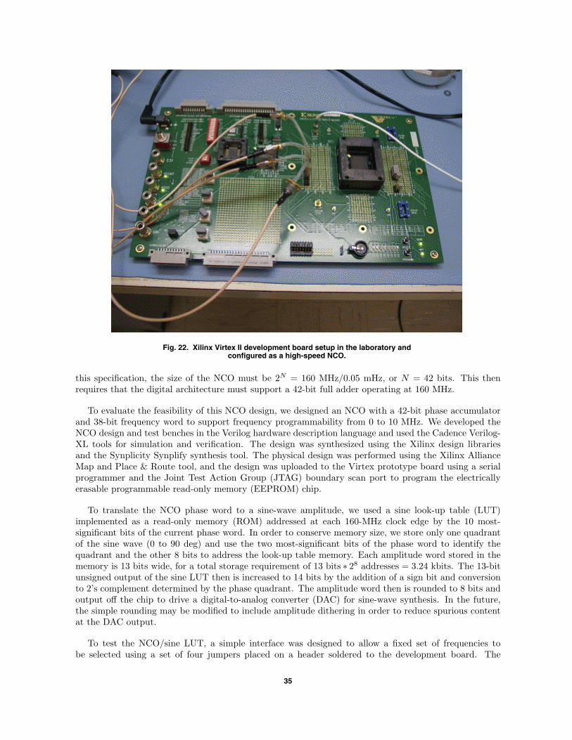
Fig. 22. Xilinx Virtex II development board setup in the laboratory andconfigured as a high-speed NCO.
this specification, the size of the NCO must be 2N = 160 MHz/0.05 mHz, or N = 42 bits. This thenrequires that the digital architecture must support a 42-bit full adder operating at 160 MHz.
To evaluate the feasibility of this NCO design, we designed an NCO with a 42-bit phase accumulatorand 38-bit frequency word to support frequency programmability from 0 to 10 MHz. We developed theNCO design and test benches in the Verilog hardware description language and used the Cadence Verilog-XL tools for simulation and verification. The design was synthesized using the Xilinx design librariesand the Synplicity Synplify synthesis tool. The physical design was performed using the Xilinx AllianceMap and Place & Route tool, and the design was uploaded to the Virtex prototype board using a serialprogrammer and the Joint Test Action Group (JTAG) boundary scan port to program the electricallyerasable programmable read-only memory (EEPROM) chip.
To translate the NCO phase word to a sine-wave amplitude, we used a sine look-up table (LUT)implemented as a read-only memory (ROM) addressed at each 160-MHz clock edge by the 10 most-significant bits of the current phase word. In order to conserve memory size, we store only one quadrantof the sine wave (0 to 90 deg) and use the two most-significant bits of the phase word to identify thequadrant and the other 8 bits to address the look-up table memory. Each amplitude word stored in thememory is 13 bits wide, for a total storage requirement of 13 bits ∗ 28 addresses = 3.24 kbits. The 13-bitunsigned output of the sine LUT then is increased to 14 bits by the addition of a sign bit and conversionto 2’s complement determined by the phase quadrant. The amplitude word then is rounded to 8 bits andoutput off the chip to drive a digital-to-analog converter (DAC) for sine-wave synthesis. In the future,the simple rounding may be modified to include amplitude dithering in order to reduce spurious contentat the DAC output.
To test the NCO/sine LUT, a simple interface was designed to allow a fixed set of frequencies tobe selected using a set of four jumpers placed on a header soldered to the development board. The
35

fixed frequencies were carefully selected to pick some frequency words that would ensure full exerciseof the 42-bit accumulator carry chain and others that were harmonically related to the clock frequencyand therefore would be expected to work at much higher clock frequencies. The NCO was exercisedusing an HP 8663 to generate the 160-MHz clock frequency. At 160 MHz, all programmed frequencieswere observed to operate correctly. The clock frequency then was increased to determine the maximumoperating frequency. The timing analyses performed by the synthesis and Place & Route tools reportedthe maximum predicted frequency of operation to be 180 MHz, but this estimate takes into accountworst-case temperature and voltage margins. At the nominal 1.5-V core and 3.3-V input/output (I/O)voltage and at ambient temperature, we were able to increase the clock frequency to nearly 280 MHzbefore seeing evidence of timing errors affecting the NCO operation. Figure 23 is a photograph of theXilinx prototype board in operation with the 4 most-significant bits of the sine LUT output displayed ona digital scope.
The original design of the DRO-PLL loop (shown in Figs. 2 through 13) uses the NCO to index asine look-up table, the output of which drives a DAC for direct digital synthesis of the ∼10-MHz variablereference. This variable reference then is mixed with the fixed 160-MHz reference oscillator, and theupper sideband is filtered and used to drive the SPD. However, we came up with a novel approach to thisarchitecture that may allow a drastic simplification of this circuit, eliminating the sine look-up table, theDAC, and the reference oscillator mixer. Figure 24 shows a comparison of the architectures we are nowinvestigating. The first is the original design using a sine look-up table and DAC. The second eliminatesthe sine LUT and the DAC by driving the reference mixer directly with the square-wave most-significantbit (MSB) output of the NCO. This approach potentially eliminates analog switching and spurious DACnoise in the PLL as well as simplifying the architecture by eliminating discrete parts. The third architec-ture takes this a step further by also pulling the reference mixer into the digital processor and generatingthe sampling phase detector reference digitally. Here, the MSB of the NCO is XOR’d (multiplied) with
Fig. 23. Xilinx Virtex II prototype board generating synthesizing sine-wave downlink using42-bit NCO and sine look-up table.
36

Fig. 24. Architectures for the NCO interface to the DRO-PLL: (a) Archi-tecture 1 uses a sine look-up table and DAC to drive the referencemixer, (b) Architecture 2 eliminates the sine look-up table and DAC bydriving the reference mixer directly with the NCO MSB, and (c) Architec-ture 3 pulls the reference mixer inside the digital processor by using adigital mixer. This third architecture also implements a digital single-sideband mixer to cancel the unwanted lower sideband mixing productand thereby relaxing the requirements on the analog filter (not shown)preceeding the sampling phase detector.
(a)
(b)
(c)
37

the synchronized clock, digitally generating the upper and lower sideband mixing products, nominally at160 MHz and 140 MHz for a 150-MHz clock and 10-MHz NCO programmed frequency. In order to relaxthe requirements on the analog filter that is required to remove the lower sideband before driving theSPD, we implemented a single-sideband mixer inside the FPGA using a delay-locked loop to generate a90-deg-delayed clock signal, and logically generating a 90-deg-delayed NCO MSB signal. The two signalsthen are analog summed outside the FPGA to cancel the out-of-phase lower sideband.
Architecture 3, depicted in Fig. 24(c), was implemented in the Xilinx Virtex II FPGA prototypeboard. By analog summing the two phases of the single-sideband mixer in a 17-ohm combiner, we wereable to demonstrate a 20-dB suppression of the lower sideband with respect to the upper sideband, anda suppression of the clock-frequency “carrier” by 35 dB. However, in our breadboard setup, we used thelow-voltage complementary metal oxide semiconductor (CMOS) output of the FPGA directly. Thesesignals are not optimized for waveform shape since they are intended simply to provide digital levels. Weexpect to see marked improvement in the lower sideband cancellation and a much cleaner waveform byfollowing the FPGA CMOS outputs with some high-speed Schmidt-trigger buffers to square up the signalbefore the analog combining.
To demonstrate the feasibility of this architecture, we used this digital single sideband (DSSB) mixerto drive the sampling phase detector, and we were able to achieve phase lock on the DRO using thismethod. However, digital switching noise and waveform irregularities produced significant close-in phasenoise, and we have not yet been able to demonstrate that this technique can be used practically for thelow-phase-noise performance we require. However, future improvements to the breadboard, including theSchmidt-trigger buffers mentioned above, should significantly improve the performance.
C. Phase Noise Measurements
An important performance parameter of the RF front-end and digital tracking architecture is the phasenoise of the synthesized downlink and uplink tracking loop. We put together a phase noise measurementsystem in the laboratory in order to investigate this parameter for our breadboard DRO and associatedcircuitry. Figure 25 is a block diagram of the phase noise test setup.
Fig. 25. Laboratory phase noise measurement system setup.
38
The device under test (DUT), the DRO in this case, is mixed with a harmonic of the precision 640-MHzreference from the HP 8663 frequency synthesizer. The IF then is beat against a reference IF generatedby the HP 8663, and the baseband phase deviations are measured using an HP 8556B Spectrum Analyzer,which is sensitive down to 100 Hz. In practice, we found that measuring phase noise with this setup atfrequency deviations of less than about 500 Hz was difficult due to interactions with the narrowbandphase-locked loop that keeps the DUT signal and the reference IF signal in quadrature by frequencymodulating the internal 10-MHz crystal oscillator in the HP 8663.
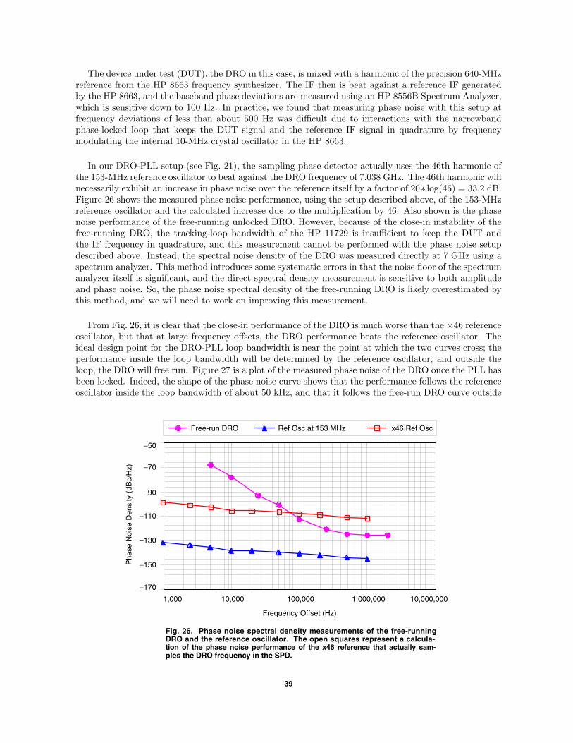
In our DRO-PLL setup (see Fig. 21), the sampling phase detector actually uses the 46th harmonic ofthe 153-MHz reference oscillator to beat against the DRO frequency of 7.038 GHz. The 46th harmonic willnecessarily exhibit an increase in phase noise over the reference itself by a factor of 20∗ log(46) = 33.2 dB.Figure 26 shows the measured phase noise performance, using the setup described above, of the 153-MHzreference oscillator and the calculated increase due to the multiplication by 46. Also shown is the phasenoise performance of the free-running unlocked DRO. However, because of the close-in instability of thefree-running DRO, the tracking-loop bandwidth of the HP 11729 is insufficient to keep the DUT andthe IF frequency in quadrature, and this measurement cannot be performed with the phase noise setupdescribed above. Instead, the spectral noise density of the DRO was measured directly at 7 GHz using aspectrum analyzer. This method introduces some systematic errors in that the noise floor of the spectrumanalyzer itself is significant, and the direct spectral density measurement is sensitive to both amplitudeand phase noise. So, the phase noise spectral density of the free-running DRO is likely overestimated bythis method, and we will need to work on improving this measurement.
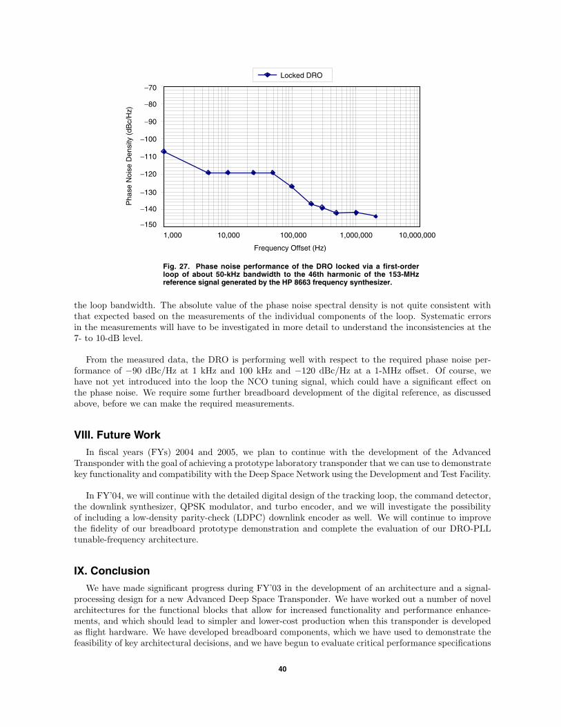
From Fig. 26, it is clear that the close-in performance of the DRO is much worse than the ×46 referenceoscillator, but that at large frequency offsets, the DRO performance beats the reference oscillator. Theideal design point for the DRO-PLL loop bandwidth is near the point at which the two curves cross; theperformance inside the loop bandwidth will be determined by the reference oscillator, and outside theloop, the DRO will free run. Figure 27 is a plot of the measured phase noise of the DRO once the PLL hasbeen locked. Indeed, the shape of the phase noise curve shows that the performance follows the referenceoscillator inside the loop bandwidth of about 50 kHz, and that it follows the free-run DRO curve outside
Pha
se N
oise
Den
sity
(dB
c/H
z)
Frequency Offset (Hz)
Free-run DRO Ref Osc at 153 MHz x46 Ref Osc
−170
1,000
Fig. 26. Phase noise spectral density measurements of the free-runningDRO and the reference oscillator. The open squares represent a calcula-tion of the phase noise performance of the x46 reference that actually sam-ples the DRO frequency in the SPD.
−150
−130
−110
−90
−70
−50
10,000 100,000 1,000,000 10,000,000
39
Locked DRO
Pha
se N
oise
Den
sity
(dB
c/H
z)
Frequency Offset (Hz)
−150
1,000
Fig. 27. Phase noise performance of the DRO locked via a first-orderloop of about 50-kHz bandwidth to the 46th harmonic of the 153-MHzreference signal generated by the HP 8663 frequency synthesizer.
−140
−130
−120
−110
−100
−90
10,000 100,000 1,000,000 10,000,000
−80
−70
the loop bandwidth. The absolute value of the phase noise spectral density is not quite consistent withthat expected based on the measurements of the individual components of the loop. Systematic errorsin the measurements will have to be investigated in more detail to understand the inconsistencies at the7- to 10-dB level.
From the measured data, the DRO is performing well with respect to the required phase noise per-formance of −90 dBc/Hz at 1 kHz and 100 kHz and −120 dBc/Hz at a 1-MHz offset. Of course, wehave not yet introduced into the loop the NCO tuning signal, which could have a significant effect onthe phase noise. We require some further breadboard development of the digital reference, as discussedabove, before we can make the required measurements.
VIII. Future Work
In fiscal years (FYs) 2004 and 2005, we plan to continue with the development of the AdvancedTransponder with the goal of achieving a prototype laboratory transponder that we can use to demonstratekey functionality and compatibility with the Deep Space Network using the Development and Test Facility.
In FY’04, we will continue with the detailed digital design of the tracking loop, the command detector,the downlink synthesizer, QPSK modulator, and turbo encoder, and we will investigate the possibilityof including a low-density parity-check (LDPC) downlink encoder as well. We will continue to improvethe fidelity of our breadboard prototype demonstration and complete the evaluation of our DRO-PLLtunable-frequency architecture.
IX. Conclusion
We have made significant progress during FY’03 in the development of an architecture and a signal-processing design for a new Advanced Deep Space Transponder. We have worked out a number of novelarchitectures for the functional blocks that allow for increased functionality and performance enhance-ments, and which should lead to simpler and lower-cost production when this transponder is developedas flight hardware. We have developed breadboard components, which we have used to demonstrate thefeasibility of key architectural decisions, and we have begun to evaluate critical performance specifications
40

such as phase noise performance of the DRO-PLL receiver tracking and downlink synthesis loops. Wehave also generated a set of detailed specifications for radio frequency integrated circuits that we wouldlike to see developed for application to this transponder architecture as well as to other ongoing andfuture radio technology development areas.
We will continue to pursue this development within the research and technology development programwith the goals of delivering a prototype transponder demonstration and gaining support for the devel-opment of an engineering model and eventual flight unit to support missions launching in the 2010 timeframe and beyond.
References
[1] J. Berner, S. Kayalar, and J. Perret, “The NASA Spacecraft Transponding Mo-dem,” Aerospace Conference Proceedings, 2000 IEEE, vol. 7, March 18–25, 2000,pp. 19209, March 2000.
[2] N. Mysoor, S. Kayalar, C. Andricos, and G. Walsh, “Performance of DielectricResonance Oscillator for Spacecraft Transponding Modem,” Aerospace Confer-ence, 2001, IEEE Proceedings, vol. 3, March 10–17, 2001, pp. 3/1222–3/1241,March 2001.
[3] J. B. Berner, J. M. Layland, P. W. Kinman, and J. R. Smith, “Regenera-tive Pseudo-Noise Ranging for Deep-Space Applications,” The Telecommunica-tions and Mission Operations Progress Report 42-137, January–March 1999, JetPropulsion Laboratory, Pasadena, California, pp. 1–18, May 15, 1999.http://tmo.jpl.nasa.gov/tmo/progress report/42-137/137G.pdf
[4] DSMS Telecommunications Link Design Handbook, TMOD 810-005, Rev. E,Module 201, JPL D-19379, Rev. E, Jet Propulsion Laboratory, Pasadena, Cali-fornia, January 15, 2001.
[5] F. Gardner, Phaselock Techniques, 2nd Edition, New York: John Wiley & Sons,Chapters 2 and 3, 1979.
[6] Wenzel Associates, Inc., Austin, Texas, Online Catalog, http://www.wenzel.com,April 2003.
41