development of a cmos pixel sensor for embedded space
TRANSCRIPT
HAL Id: tel-01126914https://tel.archives-ouvertes.fr/tel-01126914
Submitted on 6 Mar 2015
HAL is a multi-disciplinary open accessarchive for the deposit and dissemination of sci-entific research documents, whether they are pub-lished or not. The documents may come fromteaching and research institutions in France orabroad, or from public or private research centers.
L’archive ouverte pluridisciplinaire HAL, estdestinée au dépôt et à la diffusion de documentsscientifiques de niveau recherche, publiés ou non,émanant des établissements d’enseignement et derecherche français ou étrangers, des laboratoirespublics ou privés.
Development of a CMOS pixel sensor for embeddedspace dosimeter with low weight and minimal power
dissipationYang Zhou
To cite this version:Yang Zhou. Development of a CMOS pixel sensor for embedded space dosimeter with low weight andminimal power dissipation. Micro and nanotechnologies/Microelectronics. Université de Strasbourg,2014. English. �NNT : 2014STRAE021�. �tel-01126914�

UNIVERSITÉ DE STRASBOURG
ÉCOLE DOCTORALE DE PHYSIQUE ET CHIMIE PHYSIQUE
Institut Pluridisciplinaire Hubert Curien (IPHC)
THÈSE présentée par:
Yang ZHOU soutenue le : 23 Septembre 2014
pour obtenir le grade de : Docteur de l’Université de Strasbourg
Discipline: Électronique, Électrotechnique et Automatique
Spécialité: Instrumentation et Microélectronique
Development of a CMOS pixel sensor for embedded space dosimeter with low weight
and minimal power dissipation
Composition du jury:
Directeurs de thèse: M. Yann HU Professeur, Université de Strasbourg M. Jérôme BAUDOT Professeur, Université de Strasbourg
Rapporteurs externes: M. Michel PAINDAVOINE Professeur, Université de Bourgogne M. Martin POHL Professeur, Université de Genève
Examinateurs: M. Rémi BARBIER Maître de Conférences, Université de Lyon M. Olivier DORVAUX Maître de Conférences, Université de Strasbourg


Acknowledgements
I am very grateful to my supervisors Prof. Yann Hu and Prof. Jérôme BAUDOT for their support,
guidance and encouragement, and for the opportunities provided to me. I would also like to thank
China Scholarship Council (CSC) and Prof. Marc Winter, the leader of PICSEL group, for
funding my 4 years study in France.
I sincerely appreciate Prof. Jérôme BAUDOT for his guidance and fruitful discussions in the
physics part, offering the analysis of the prototype test results, and providing the corrections and
suggestions for this manuscript. I would also like to thank Cyril Duverger, a master student in
physics, for his contribution in the Monte-Carlo sensor response simulations of this work.
I would like to thank all the colleagues in microelectronics group: Christine Hu-Guo, Claude
Colledani, Wojciech Dulinski, Xiaochao Fang, Andrei Dorokhov, Frédéric Morel, Maciej Kachel,
Abdelkader Himmi, Yunan Fu, Ying Zhang, Wei Zhao, Tianyang Wang, Isabelle Valin, Hung
Pham, Guy Doziere, Christian Illinger and Sylviane Molinet for their suggestions, helps and
technical supports during the sensor design.
I owe my gratitude to Kimmo Jaaskelainen for his fully support during the test of the prototype,
including the PCB design and test bench set up. I also appreciate Gilles Claus and Mathieu Goffe
for their suggestions and helps during the prototype test.
Last but not least, I would like to thank my parents for their unconditional love, support and
understanding.
Strasbourg, 09/10/2014


i
Contents
Table of Contents ...........................................................................................................................................i
List of Figures ................................................................................................................................................ v
List of Tables ................................................................................................................................................. ix
Résumé en Français ....................................................................................................................................... 1
Introduction ................................................................................................................................................. 13
1 Ionization based particle detection ....................................................................................................... 17
1.1 Interactions of particles with matter .................................................................................................. 18
1.1.1 Interaction of electrons ............................................................................................................... 18
1.1.2 Interaction of protons and ions ................................................................................................... 20
1.1.3 Interaction of photons ................................................................................................................. 22
1.2 Properties of Radiation Detector ....................................................................................................... 23
1.3 Silicon detectors ................................................................................................................................ 26
1.3.1 Silicon detector physics .............................................................................................................. 26
1.3.2 Radiation damages ..................................................................................................................... 30
1.3.3 Single diode detectors ................................................................................................................ 33
1.3.4 Pixelated detectors ...................................................................................................................... 33
1.4 Conclusion ......................................................................................................................................... 38
2 MAPS for particle tracking detection ................................................................................................... 42
2.1 Specifications for particle tracking .................................................................................................... 42
2.1.1 Physics goals Driven Specifications ........................................................................................... 43
2.1.2 Environment Driven Specifications ........................................................................................... 43
2.2 MAPS technology ............................................................................................................................. 44
2.2.1 Global architecture and fast readout strategy ............................................................................. 45
2.2.2 Basic pixel architectures ............................................................................................................. 46
2.2.3 Sources of Noise in MAPS ......................................................................................................... 48
2.3 MIMOSA 26 ..................................................................................................................................... 51
2.3.1 Pixel ............................................................................................................................................ 52
2.3.2 Analogue to Digital Conversion ................................................................................................. 53
2.3.3 Zero suppression ......................................................................................................................... 54

Table of contents
ii
2.3.4 Performances .............................................................................................................................. 54
2.4 Conclusions ....................................................................................................................................... 55
3 Space radiation monitoring ................................................................................................................... 58
3.1 The energetic particle environment ................................................................................................... 58
3.2 Space radiation monitors ................................................................................................................... 60
3.2.1 The Geiger-Mueller tube ............................................................................................................ 61
3.2.2 The Scintillating Fibre Detector (SFD) ...................................................................................... 61
3.2.3 RadFETs (MOS structures sensitive to ionizing radiation) ........................................................ 62
3.2.4 The Standard Radiation Environment Monitor (SREM) ............................................................ 62
3.2.5 Pixel sensors ............................................................................................................................... 63
3.3 From measurement requirements to design specifications: simulation methods and results ............ 65
3.3.1 The choice of sensor sensitive area, pixel pitch size and readout speed .................................... 65
3.3.2 Simulation of pixel response ...................................................................................................... 67
3.3.3 Complementary Monte-Carlo simulation and estimated performances ..................................... 81
3.4 Conclusions ....................................................................................................................................... 84
4 General COMETH architecture ........................................................................................................... 87
4.1 The analogue signal processing ......................................................................................................... 87
4.2 Analogue to Digital conversion ......................................................................................................... 88
4.2.1 ADC definition ........................................................................................................................... 89
4.2.2 ADC Characterization ................................................................................................................ 91
4.2.3 Specifications for the ADC used in COMETH .......................................................................... 95
4.3 The embedded digital signal processing ............................................................................................ 96
4.4 Global architecture of COMETH ...................................................................................................... 97
5 Analogue signal processing .................................................................................................................. 100
5.1 Pixel design ..................................................................................................................................... 100
5.1.1 The CS pre-amplify stage ......................................................................................................... 103
5.1.2 The SF stage ............................................................................................................................. 106
5.1.3 The global pixel performance ................................................................................................... 107
5.2 Test of the pixel matrix ................................................................................................................... 108
5.2.1 Experimental set-up .................................................................................................................. 108
5.2.2 Noise performances .................................................................................................................. 110
5.2.3 Test with the 55
Fe source .......................................................................................................... 112

Table of contents
iii
5.2.4 Test with a Beta minus source .................................................................................................. 114
5.2.5 Test with infrared laser illumination ........................................................................................ 117
5.3 Conclusion and perspectives ........................................................................................................... 118
6 From analogue to digital ...................................................................................................................... 121
6.1 Standard ADC architectures ............................................................................................................ 122
6.1.1 Flash ADC ................................................................................................................................ 122
6.1.2 Pipelined ADC ......................................................................................................................... 123
6.1.3 Successive approximation ADC ............................................................................................... 124
6.2 Design of the column ADC for COMETH ...................................................................................... 125
6.2.1 Global architecture and processing principle ........................................................................... 126
6.2.2 Design of the S/H circuit .......................................................................................................... 130
6.2.3 Design of the comparator ......................................................................................................... 134
6.2.4 Layout and estimated power dissipation .................................................................................. 140
6.3 Test of the column level ADC ......................................................................................................... 141
6.3.1 Characteristics of a single ADC ............................................................................................... 141
6.3.2 Characteristics of the 32 columns............................................................................................. 142
6.4 Solutions for the ADC performance improvement ......................................................................... 144
7 Embedded digital signal processing .................................................................................................... 148
7.1 Operation principle .......................................................................................................................... 148
7.2 The hardware system ....................................................................................................................... 151
7.2.1 The temporary memory block .................................................................................................. 153
7.2.2 The finite state machine_1 ....................................................................................................... 154
7.2.3 The cluster data sum block ....................................................................................................... 154
7.2.4 The finite state machine_2 ....................................................................................................... 155
7.2.5 The Counter and final output .................................................................................................... 156
7.2.6 Layout and estimated power dissipation .................................................................................. 157
7.3 Reconstruction performances .......................................................................................................... 158
7.3.1 Tricky cluster cases could be reconstructed correctly .............................................................. 159
7.3.2 Tricky cluster cases which lead to reconstruction failures ....................................................... 161
7.3.3 Performances for clusters merging ........................................................................................... 162
7.4 Conclusions ..................................................................................................................................... 162
General conclusions ................................................................................................................................. 164

Table of contents
iv
Test board schematic for the prototype of COMETH ......................................................................... 166
Publications and communications 182
Abstract 183

v
List of Figures
Figure 1.1: Sketch of electron tracks might appear in material. .................................................................. 19
Figure 1.2: Mean CSDA range in silicon for electrons (left) and proton (right). ........................................ 20
Figure 1.3: Straggling functions in silicon for 500 MeV pions, normalized to unity at the most probable
value �. The width � is the full width at half maximum. ......................................................................... 21
Figure 1.4: Regions where the photoelectric effect, Compton effect and pair production dominate as a
function of the photon energy and the atomic number of the absorber. ...................................................... 22
Figure 1.5: Examples of good and poor energy resolutions ........................................................................ 24
Figure 1.6: Definition of detector resolution. .............................................................................................. 24
Figure 1.7: Incoming events recorded with non-paralyzeble (a) and paralyzable (b) devices .................... 25
Figure 1.8: Approximation of an abrupt p-n junction: space charge density, electric field distribution, and
electrostatic potential distribution. .............................................................................................................. 27
Figure 1.9: Electron and hole velocities vs. the electric field strength in silicon. ....................................... 29
Figure 1.10: A typical CMOS device with elements of a parasitic thyristor. .............................................. 32
Figure 1.11: Typical CCD detectors with three gates for each pixel. ......................................................... 34
Figure 1.12: Illustration of a hybrid pixel detector. ..................................................................................... 35
Figure 1.13: Cross section view of a CPS pixel. ......................................................................................... 36
Figure 2.1: Column parallel readout principle. ........................................................................................... 45
Figure 2.2: The classical single pixel cell: (a) schematic, (b) timing diagram showing the operation and the
signal shape. ................................................................................................................................................ 46
Figure 2.3: Self-biased pixel cell: (a) schematic, (b) timing diagram showing the operation and the signal
shape. ........................................................................................................................................................... 47
Figure 2.4: Pixel topology with in pixel amplification and CDS. ............................................................... 50
Figure 2.5: Illustration of Random Telegraph Signal (RTS). ...................................................................... 50
Figure 2.6: Pixel output noise distribution at the sensor output. ................................................................. 51
Figure 2.7: MIMOSA 26 block diagram. .................................................................................................... 52
Figure 2.8: Pixel schematic of MIMOSA 26. .............................................................................................. 53
Figure 2.9: Architecture of the column-level discriminator. ....................................................................... 53
Figure 3.1: cross section of radiation belts. ................................................................................................. 59
Figure 3.2: Earth’s radiation belts as represented by the standard AP8 and AE8 models. The two panels show contour plots of integral proton flux > 10 MeV (left) and integral electron flux > 0.6 MeV (right).
Whereas electrons populate the inner and outer zone, protons are only trapped in the inner zone. ............ 60
Figure 3.3: Picture of SREM flight model and the schema of its two detector head. ................................. 63
Figure 3.4: Block diagram (left) and photo (right) of HMRM structure. It features a stack of four CPS (S1
to S4), where S1 and S2 in close proximity. ............................................................................................... 64

Table of figures
vi
Figure 3.5: relations between speed, accuracy, power, sensitive area and pitch size. ................................. 65
Figure 3.6: Incident proton and electron energy versus their energy loss used to generate e-/h pairs per µm
in silicon, the vertical dashed lines indicate energy intervals concerned. ................................................... 68
Figure 3.7: total energy loss of proton in 14 µm thick silicon with respect to its kinetic energy. ............... 69
Figure 3.8: Schematic diagram of particle range in the cross section of epitaxial layer. ............................ 70
Figure 3.9: Simulation result of signal over pixels for a typical situation: particles hit in junction region of
four adjacent pixels at normal incidence. .................................................................................................... 71
Figure 3.10: Simulation result of signal over pixels for a typical situation: particles hit in the center of a
pixel at normal incidence. ........................................................................................................................... 72
Figure 3.11: sensor responses for various particles with respect to number of pixels fired (threshold 200 e-
) and totally number of e- collected from fired pixels. For each kind of particle, there are 3 points represent
3 incident situations on behalf of hit position or angular effects. Two of them are normal incident with
different position relative to the sensing diode, another is θ=80° as illustrated in figure 3.8. .................... 74
Figure 3.12: Total e- generated by various particles with respect to the number of pixels with collected
charges higher than 200 e-. .......................................................................................................................... 75
Figure 3.13: Total e- generated by various particles with respect to sum of 3-bit ADC counts for all the
pixels in a cluster (a) and its sub-region (b). ............................................................................................... 76
Figure 3.14: Total e- generated by various particles with respect to sum of 4-bit ADC counts for all the
pixels in a cluster (a) and its sub-region (b). ............................................................................................... 77
Figure 3.15 : An example for the basic operation principle of the digital processing. ................................ 80
Figure 3.16: Monte-Carlo simulation results of energy loss in the sensor’s sensitive area versus particle incident energy. ........................................................................................................................................... 81
Figure 3.17: Monte-Carlo simulation results of incident particle energy versus triggered cluster ADC
counts. ......................................................................................................................................................... 82
Figure 3.18: Reconstructed energy versus deposited energy. ..................................................................... 83
Figure 3.19: Number of clusters reconstructed per frame versus number of particles effectively impinging
the sensor. .................................................................................................................................................... 83
Figure 4.1: Analogue signal processing architecture of COMETH. ........................................................... 88
Figure 4.2: ADC description. ...................................................................................................................... 89
Figure 4.3: Typical transfer curve of an N-bit ADC. .................................................................................. 90
Figure 4.4: Comparator Circuit and Transfer Function. .............................................................................. 90
Figure 4.5: Offset and gain error of an N-bit ADC. It is assumed that all other errors are not presented. .. 92
Figure 4.6: Example Transfer Characteristic of an N-bit ADC Showing DNL and INL. ........................... 93
Figure 4.7: Emulated COMETH 3-bit digitized response of one frame...................................................... 97
Figure 4.8: Global architecture of COMETH (a) and the layout (3.5 mm × 4 mm) of the first reduced scale
prototype (b). ............................................................................................................................................... 98
Figure 5.1 : (a) Schematic of the pixel and, (b) related timing. ................................................................. 101
Figure 5.2: Common source amplifier stage used inside the pixel. ........................................................... 103
Figure 5.3: Static characteristics of the CS stage under different W/L values of M1. .............................. 105

Table of figures
vii
Figure 5.4: Static characteristics of the CS stage with W/L ratio of M1 equals to 0.55µm/12µm. ........... 105
Figure 5.5: Gain and input-output voltage characteristic of the SF stage. ................................................ 106
Figure 5.6: Simulation of the in-pixel offset cancellation operation. ........................................................ 107
Figure 5.7: Set-up for laboratory test. ....................................................................................................... 109
Figure 5.8: Distribution of pedestal values (a) and temper noise (b) for the sub-array with 8×32 pixels. 112
Figure 5.9: Noise of a normal pixel (a), and a noisy pixel with RTS noise (b). ........................................ 112
Figure 5.10: Collected charge distribution observed with a 55
Fe source. Fig. (a) shows the entire
distribution while Fig. (b) displays a zoom on the calibration peak. ......................................................... 113
Figure 5.11: Cluster collected charge with the 55
Fe source: 3×3 pixels (a) and 5×5 pixels (b). The lines
represent gaussian fits to estimate the MPV of the distribution. ............................................................... 114
Figure 5.12: Seed pixel collected charge with a 90
Sr ß- source. ................................................................ 114
Figure 5.13: Percentage of pixels with charge > 120 e- with a
90Sr β- source (a) and cluster multiplicity
with charge > 120 e- (b). ........................................................................................................................... 115
Figure 5.14: Accumulated charge with different number of pixels in a cluster. ....................................... 116
Figure 5.15: SNR of the seed pixel to electrons. ....................................................................................... 117
Figure 5.16: Evolution of the pixel response to a linear increase of the laser illumination, for three
different laser currents. The laser illumination amplitude depends linearly on the number of laser pluses
shot during one sensor frame. .................................................................................................................... 118
Figure 5.17: layout of a single pixel. ......................................................................................................... 119
Figure 6.1: ADC architecture vs Resolution and sampling rate. ............................................................... 121
Figure 6.2: Architecture of an N-bit flash ADC. ....................................................................................... 122
Figure 6.3: Block Diagram of a Typical Pipelined ADC. ......................................................................... 123
Figure 6.4: Basic architecture of an N-bit successive approximation ADC. ............................................. 124
Figure 6.5: Example of the searching process of a 4-bit SAR conversion. The digital output is 0101. .... 125
Figure 6.6: Expected transfer function of the 3-bit ADC in COMETH. ................................................... 126
Figure 6.7: Global architecture of the column 3-bit SAR ADC for COMETH. ....................................... 127
Figure 6.8: Timing diagram for the column 3-bit SAR ADC. .................................................................. 128
Figure 6.9: Equivalent ADC circuit during the SET phase. ...................................................................... 128
Figure 6.10: Equivalent ADC circuit for the threshold comparison. ......................................................... 129
Figure 6.11: Equivalent ADC circuit for the conversion of the MSB. ...................................................... 129
Figure 6.12: Sampling structure: (a) parallel sampling, (b) series sampling. ............................................ 130
Figure 6.13: Schematic of the S/H circuit. ................................................................................................ 131
Figure 6.14: Timing diagram of the S/H circuit. ....................................................................................... 132
Figure 6.15: Schematic of the unit gain buffer (a); its transient response (b) and static response (c). ...... 133
Figure 6.16: Column level offset cancellation simulation results. ............................................................ 134
Figure 6.17: Typical comparator architecture. .......................................................................................... 135
Figure 6.18: Input offset storage architecture. ........................................................................................... 135
Figure 6.19: Output offset storage architecture. ........................................................................................ 136
Figure 6.20: The architecture (a) and its operation timing (b). ................................................................. 138
Figure 6.21: schematic of the preamplifier used in the comparator. ......................................................... 138

Table of figures
viii
Figure 6.22: Schematic of the dynamic latch. ........................................................................................... 139
Figure 6.23: layout of the column-level ADC. .......................................................................................... 141
Figure 6.24: Transfer functions of ADC31 and the expected ideal one. ................................................... 141
Figure 6.25: DNL (a) and INL (b) characteristics of ADC31. .................................................................. 142
Figure 6.26: Transfer functions of the 32 column ADCs (enlarged LSB value). ...................................... 142
Figure 6.27: Column dispersion of the first bit: (a) zoom of the 1st bit; (b) fixed pattern noise. .............. 143
Figure 6.28: Overview of the ADC designed for the HMRM ASIC. An 8-bit trimming DAC compensates
the comparator offset. ................................................................................................................................ 144
Figure 6.29: Results with compensation: (a) transfer functions of 32 columns; (b) noise of the first bit. 145
Figure 6.30: The column ADC architecture with Switched-DAC for comparator references. ................. 145
Figure 7.1: Principle of the clusterization and summation. ....................................................................... 149
Figure 7.2: the digital processing hardware system. ................................................................................. 152
Figure 7.3: Timing for the digital processing system (not scaled). ........................................................... 153
Figure 7.4: interface of the temporary memory block. .............................................................................. 153
Figure 7.5: interface of the Finite state machine_1. .................................................................................. 154
Figure 7.6: column cell interfaces of the cluster data sum block. ............................................................. 155
Figure 7.7: Architecture of the “Sum Core”. ............................................................................................. 156
Figure 7.8: basic cell of finite state machine_2. ........................................................................................ 156
Figure 7.9: the interface of the counter. .................................................................................................... 157
Figure 7.10: Physical layout of the digital processing stage. .................................................................... 158
Figure 7.11: Examples of “dead” pixels in the middle of the cluster first row. ........................................ 159
Figure 7.12: Examples of “dead” pixels in the middle of the cluster edge columns. ................................ 160
Figure 7.13: Examples of “dead” pixels in the center or last row of a cluster. ......................................... 160
Figure 7.14: Examples of some two adjacent “Dead” pixels cases. .......................................................... 160
Figure 7.15: Reconstruction failure examples of two adjacent “dead” pixels in the center of a cluster. .. 161
Figure 7.16: Reconstruction failure examples of two adjacent “dead” pixels. .......................................... 161
Figure 7.17: Reconstruction examples of two cluster merging. ................................................................ 162
Figure A.1: Schematic of the proximate test board of the prototype of COMETH. ................................. 170
Figure A.2: Schematic of the auxiliary test board of the prototype of COMETH. ................................... 181

Table of figures
ix
List of Tables
Table 2.1: Performance of MIMOSA 26. .................................................................................................... 54
Table 3.1: probability of hits pile-up with respect to sensor operation speed and cluster size. ................... 66
Table 3.2: Simulated mean values of total number of e- generated in the epitaxy layer by several particles
at normal incidence; and the numbers for these percentages relative to Figure 3.5. E and P represent
electrons and protons respectively; all the numbers in this table have a unit of e-. .................................... 72
Table 3.3: Simulated mean values of total number of e- generated in the epitaxy layer by several particles
at normal incidence; and the numbers for these percentages relative to Figure 3.6. E and P represent
electrons and protons respectively; all the numbers in this table have a unit of e-. .................................... 73
Table 7.1: Estimated power dissipation of each functional cell and the whole digital processing stage. . 158


1
Résumé en Français
Ce travail de thèse cherche à étendre le domaine d'application des capteurs à pixels CMOS (CPS)
dont l'état de l'art est donné par les développements menés dans le groupe PICSEL de l'IPHC.
L'objectif est de concevoir un capteur pour la dosimétrie des particules ionisantes dans l'espace,
qui présente les mêmes performances que les compteurs actuels, mais avec une dissipation de
puissance réduite d'un ordre de grandeur, qu'un poids, un volume d'encombrement et un coût
moindres. Le caractère monolithique des CPS les place comme candidats pour un tel système
compact embarqué sur satellite.
L'orbite terrestre est un environnement composé d'une grande variété de particules chargées
énergétiques dominée par les protons et les électrons [1, 2]. Leur flux total omnidirectionnel peut
atteindre 107 Part./cm
2/s, et couvre des énergies de plusieurs ordres de grandeur (allant de 0.1
MeV à 400 MeV pour les électrons et de 0.1 MeV à 7 MeV pour les protons). L'interaction de ces
particules avec les instruments de bord provoque des dégradations par effet cumulatif ou
individuel (single event effect) des dispositifs électroniques. Ces effets conduisent à des
disfonctionnements, réduisent la longueur des missions et peuvent induire la destruction du
satellite. Par ailleurs, les missions habitées engendrent des besoins en sécurité encore plus
importants.
Les données fournies par les dosimètres permettent de déterminer les risques et de corréler les
effets des radiations à l'environnement. Il en résulte une amélioration de la préparation des
missions, des recommandations) pour la conception des engins spatiaux et la possibilité d' alertes
en temps reel.
Actuellement, les dosimètres peuvent se répartir en deux catégories: les instruments scientifiques
et les instruments de support. Les premiers favorisent la précision scientifique et peuvent
atteindre un poids et une consommation relativement importants (supérieurs à 1kg et 1W). Au
contraire, les seconds présentent des fonctionnalités limités, avec peu ou sans capacité de
discrimination des particules. Dans la mesure où les dommages ionisants dépendent fortement du
type et de l'énergie des particules, la discrimination offrirait une amélioration substantielle de ces
dispositifs. Par conséquent le développement d'un dosimètre précis mais d 'une faible empreinte
ouvrirait de nouvelles perspectives pour la dosimétrie spatiale.
Les informations diffusées par l’agence spatiale européenne (ESA) permettent de dégager les spécifications suivantes pour un dosimètre ou compteur embarqué de radiation:
1. petit volume (de l’ordre de 1 cm3), faible poids (environ 20g), faible puissante dissipée
(inférieure à 200 mW);
2. capacité à estimer l’énergie des particules primaires dont le flux est mesuré ;

Résumé en Français
2
3. une gamme dynamique choisie afin de maximiser la différentiation des particules
primaires sur la toute la gamme d’énergie attendue dans l’orbite terrestre ; 4. information de dose reçue en temps réel ;
5. taux mesurable de particules correspondant à un flux omnidirectionnel intégré de
107·cm
-2·s
-1 ;
6. identification de l’espèce des particules détectées ;
7. radio-tolérance pour une dose totale ionisante d’au moins 100 kRad (1 kGy).
Les capteurs à pixels CMOS représentent le candidat le plus prometteur pour répondre à ces
spécifications, grâce notamment aux avantages suivants vis-à-vis des technologies concurrentes.
1. L’intégration de l’électronique de conditionnement analogique et numérique du signal au sein du même circuit contenant la couche sensible de pixels, favorise une petite taille et
permet de réduire la puissance consommée.
2. Les développements de CPS pour les applications auprès des collisionneurs de particules,
ont montré comment atteindre un bruit équivalent à une charge aux alentours de 10
électrons par pixel, en tirant parti de la petite taille du nœud de collection des charges, qui entraine un faible courant de fuite et une petite capacité. Par ailleurs, en prenant en
compte l’épaisseur de la couche sensible, entre 15 et 20 µm, le signal le plus faible attendu est de l’ordre de quelques centaines d’électrons. Le rapport signal-à-bruit
correspondant dépasse donc 20 et assure une excellente sensibilité aux particules à
détecter.
3. La génération et la collection des charges s’effectuent dans une couche sensible continue, la pixellisation étant réalisée à un niveau supérieur au sein de la couche électronique. Le
dispositif ne présente donc pas de zone insensible, c’est à dire un fill factor de 100%.
4. L’épaisseur totale du capteur peut être diminuée jusqu’à 50 µm par des processus industriels simples et peu couteux. Le capteur est alors une feuille mince dont
l’intégration dans un système de détection, éventuellement à plusieurs capteurs, devient
très simple et peu encombrante.
5. Les technologies CMOS profondément submicroniques utilisées actuellement pour la
fabrication des capteur à pixels, assurent une radio-tolérance, pour les structures
classiques, qui dépasse aisément 100 kRad. Les développements des capteurs à pixels
CMOS ont par ailleurs démontré que, dans ces technologies, le système de collection des
charges tolérait également des doses bien au delà de 100 kRad ainsi que des fluences de
particules non-ionisantes au-delà de 1012
neq/cm2 .
A cause de ces avantages, le projet HMRM (Highly Miniaturized Radiation Monitor) des
laboratoires RAL du STFC et Imperial college, soutenu par l'ESA, s'appuie sur un imageur
CMOS [3]. Mais il ne s'agit pas de la conception d'un capteur dédié à l'application, contrairement
aux ambitions de cette thèse.

Résumé en Français
3
Les travaux du groupe PICSEL de l'IPHC se sont essentiellement attachés à démontrer et
explorer les capacités des CPS pour la trajectométrie des particules chargées. La série des
prototypes de capteur MIMOSA, conçus et faits fabriquer par le groupe, a permis d’améliorer suffisamment leurs performances pour représenter l’état-de-l’art actuel des CPS pour cette application. Le capteur MIMOSA 26 en est l’illustration, il est le premier capteur de grande taille (2 cm
2 de surface active) rapide (10 000 trames par seconde) incorporant un traitement du signal
permettant la réduction des données [4]. La figure 1 en donne un schéma fonctionnel.
Figure 1: digramme fonctionnel du capteur MIMOSA 26.
Fabriqué en technologie AMS 0.35 µm, MIMOSA 26 comprend une matrice de pixels de taille
18.4x18.4 µm2, offrant une résolution spatiale meilleur que 4 µm. Avec 576 rangées et 1152
colonnes, la surface active atteint 224 mm2. Le cheminement des signaux se résume en trois
étapes principales. Chaque pixel intègre une pré-amplification et un double échantillonnage
corrélé. Les colonnes se terminent chacune par un comparateur qui numérise le signal sur 1 bit.
Enfin les signaux binaires sont filtrés par un algorithme de suppression des zéro qui réduit les
données aux seules adresses des pixels touchés. Le circuit opère selon une lecture en volet roulant
où tous les pixels d’une rangée sont traités simultanément. L’ensemble de ces fonctionnalités permet d’atteindre une fréquence élevée de lecture continue de 10 000 images par seconde pour
une puissance dissipée de l’ordre de 300 mW/cm2. Par ailleurs, la radiotolérance du circuit
correspond à des performances inchangées jusqu’à un dose ionisante totale de 3 kGy.
Cependant les capteurs conçus pour la physique des hautes-énergies ne répondent sas directement
aux spécifications du comptage de particules embarqué. Les différences d'objectifs et
d'environnement justifient une stratégie de conception particulière pour la dosimétrie spatiale.
En premier lieu, notons que le traitement analogique obéit à des contraintes différentes pour les
deux applications, du fait des domaines d'énergies concernées. La trajectométrie des particules au

Résumé en Français
4
minimum d'ionisation requiert des circuits analogiques avec un gain important et un bruit faible.
Les particules de l'environnement spatial couvre un spectre en énergie beaucoup plus important ;
et les énergies déposées correspondantes couvrent plusieurs ordres de grandeur. Par conséquent le
traitement analogique du dosimètre spatial doit réaliser un compromis entre gain et limite de
saturation. Une autre contrainte provient du flux élevé, qui, combiné aux signaux de grande
amplitude, nécessite une stratégie de remise à zéro de la diode de collection des charges très
efficace. Enfin la linéarité sur une grande dynamique exige une numérisation sur plus d’un bit.
Les critères de numérisation diffèrent également entre les deux applications. Le dosimètre ne
cherche pas à localiser les particules mais à les distinguer afin de les compter. La dose est estimée
avec la somme des énergies mesurées. Pour cette raison, la numérisation doit disposer de
plusieurs bits, là où la localisation peut se satisfaire d'un seul et donc d'un simple comparateur.
Enfin, la gestion finale des données numérisées poursuit une logique totalement différente. Pour
la trajectométrie, l'objectif consiste à réduire la quantité d'information à transmettre, la stratégie
consiste à ne sortir du circuit que les positions des quelques pixels touchés. Les positions sont
reconstruites grâce à des algorithmes exploités sur des processeurs externes au circuit. Pour un
système embarqué sur satellite, de telles ressources ne sont pas disponibles. Le traitement final
intégré au circuit doit donc délivrer des informations de haut niveau directement exploitables en
termes de dosimétrie.
Au final, les trois caractéristiques principales d’un capteur à pixels CMOS adapté à la mesure des radiations dans l’espace sont : une amplification analogique avec un gain moderé et une linéarité sur une large gamme dynamique ; un convertisseur analogique-numérique de quelques bits; et un
traitement numérique qui incorpore un algorithme de calcul de dose.
Si des éléments analogiques existant répondent déjà aux critères édictés, le défi premier de cette
thèse consiste à démontrer que leur intégration dans un capteur ne dégrade pas le bruit de ce
dernier et permet ainsi de préserver la sensibilité aux particules à détecter. La seconde difficulté
correspond à l’intégration d’un algorithme complexe au sein du circuit afin de le convertir en un
véritable dosimètre autonome.
Résumé des travaux
Les travaux effectués comprennent à la fois les études de définition des paramètres d’un capteur CMOS complet répondant aux besoins de l’application ainsi que la réalisation et le test d’un prototype. Ce premier capteur prototype, fabriqué dans une technologie CMOS 0.35 µm, ne
comprend pas la partie finale du traitement des informations des pixels permettant le calcul du
flux de particules en fonction de leur énergie et de leur nature. Cependant, cet algorithme a été
entièrement synthétisé et tester par simulation.
Partie 1: Etude du concept

Résumé en Français
5
Les deux contraintes principales sur les paramètres du compteur proviennent du flux des
particules et de la forme des impacts de celle-ci sur la matrice de pixels. Par ailleurs, la nécessité
de limiter la taille du circuit et sa consommation de puissance plaide pour un faible nombre de
pixels. L’optimisation obtenue correspond à une surface sensible de 10 mm2, comprenant une
matrice de pixels de 50 µm de pas. Avec un temps de lecture de 20 µs, il est possible à la fois de
distinguer individuellement les impacts pour le flux le plus important de 107 /cm
2/s avec une
erreur marginale (1%) et de mesurer en 1 seconde le flux le plus faible de 103 /cm
2/s avec une
incertitude de 10%.
Une simulation détaillée permet de vérifier que les paramètres ci-dessous répondent aux
spécifications. Elle comprend les quatre étapes suivantes.
1) L’énergie des particules traversant le compteur est déterminée par le logiciel GEANT4
sur la base d’une simulation MonteCarlo. La figure 2 illustre l’écart entre les distributions pour les électrons et les protons et indique la possibilité de distinguer ces deux types de
particules jusqu’à une énergie de 50 MeV, sur la base de l’énergie déposée par chaque
impact.
2) Un model paramétrique de la réponse des CPS, couplé à un tirage aléatoire, permet de
convertir l’énergie déposée en un signal sur chaque pixel de la matrice.
3) Le signal de chaque pixel est numérisé sur 3 bits pour reproduire l’effet du convertisseur analogique-numérique au sein du capteur.
4) Les informations de tous les pixels d’une ligne sont traités simultanément par un algorithme qui reconnaît les amas de pixels adjacents générés par l’impact des particules. L’algorithme calcule en sortie la somme des signaux obtenus sur chaque pixel de l’amas. Sa logique correspond à un traitement séquentiel, qui peut être implémenté directement
dans le capteur.
Figure 2: Distribution de l’énergie déposé dans le compteur, obtenue par simulation, en fonction de
l’énergie incidente des particules.

Résumé en Français
6
Les résultats finals de la simulation complète sont représentés par la figure 3. Pour chaque trame
de lecture du capteur, jusqu’à 20 (correspondant au flux maximum) particules impactent la matrice de pixel, avec une distribution d’énergie incidente variant de 1 à 100 MeV. La figure montre que l’énergie déposée peut-être reconstruite avec une résolution d’environ 10%, suffisante pour l’application visée. Par ailleurs, il apparaît que le comptage des particules est
parfaitement assuré jusqu’à une multiplicité de 16 impacts simultanés. Au delà, un effet de saturation apparaît lié à la superposition des amas de pixels.
Figure 3: Simulation des performances de mesure de l’énergie déposée et de comptage du capteur
proposé. A gauche : distribution de l’énergie reconstruite en fonction de l’énergie effectivement déposée. A droite : nombre de particules identifiés en fonction du nombre de particules ayant effectivement
impactées le capteur.
Partie 2: Conception et test du prototype
Le prototype cherche à valider le concept déterminé par l’étude en simulation. Il reprend les caractéristiques exactes des pixels mais sur une surface plus faible 1.6x1.6 mm
2 correspondant à
une matrice de 32x32 pixels. Chaque pixel comprend un étage de pré-amplification et réalise le
double échantillonnage corrélé permettant de fournir une valeur directement exploitable. La
matrice est lue selon un mode en volet-roulant, ligne-à-ligne, en un temps inférieur à 20 µs qui
correspond également au temps d’intégration du signal. Chaque colonne se termine par un convertisseur analogique-numérique réalisant une conversion sur 3 bits toutes les 240 ns (temps
de lecture d’une ligne de la matrice).
L’algorithme numérique de traitement des données n’est pas inclus dans le prototype. Ce type de circuiterie purement numérique est facilement testable grâce aux logiciels de simulation fournis
avec les outils (CADENCE) de dessin assisté par ordinateur permettant de concevoir les circuits
CMOS.

Résumé en Français
7
Le prototype a été entièrement dessiné sous CADENCE, et ses performances électriques ont été
validé d’abord par simulation avec le même outil. Le capteur a été fabriqué en 2012 et testé en 2013.
(a) (b)
Figure 4: Schéma physique (a) et schéma fonctionnel (b) du capteur prototype
Traitement analogique du signal au sein du pixel :
Deux fonctionnalités principales sont requises au sein du pixel : d’une part amplifier le signal afin
d’assurer un rapport signal-à-bruit suffisant pour l’efficacité de détection ; et d’autre part effectuer un double échantillonnage corrélé (CDS pour correlated double sampling) afin de
condition le signal pour la numérisation. L’architecture du pixel et son fonctionnement temporel
sont illustrés par la figure 5. L’élément sensible collectant les charges d’ionisation est une simple diode. Elle est connectée directement à un amplificateur de type source commune. Un autre
amplificateur connecté en série avec une capacité et deux transistors de réinitialisation (RST1,
RST2 sur le schéma) assurent le CDS. Finalement un amplificateur suiveur relie la sortie du pixel
au convertisseur analogique-numérique en bout de colonne. Deux transistors de colonne sont
nécessaire pour déclencher la mémorisation des niveaux de base (CALIB) et la lecture (RD).
L’ensemble de cette implantation exploite uniquement des transistors de type NMOS, puisque tout transistor PMOS implique un puit de type N qui rentrerait en compétition avec la diode pour
la collection des signaux.
Pixel Pixel Pixel Pixel
Pixel Pixel Pixel Pixel
Pixel Pixel Pixel Pixel
Pixel Pixel Pixel Pixel
Per Column 3-bit ADC
Ro
w s
elec
tio
nL
og
ic B
lock
Colu
nm
ou
tpu
t li
ne
Output
Multiplexer

Résumé en Français
8
(a) (b)
Figure 5: Schématique électrique du pixel (a) et chronogramme de la
séquence de lecture (b).
Le prototype a été caractérisé en laboratoire en utilisant plusieurs mode de stimulation,
bombardement avec des rayons X monochromatiques (source de 55
Fe) et des rayons ß (source de 90
Sr), et illumination par un laser infrarouge (longueur d’onde 1063 nm) pulsé et focalisé (spot de 5 µm) et d’intensité variable. Les tests ont permit d’établir que la charge équivalent au bruit est de l’ordre de 28 e- et conduit à un rapport signal-à-bruit de 13 pour les électrons (correspondant
au signal le plus faible, voir figure 6a). La linéarité de la sortie des pixels a été établie pour une
charge d’entrée entre 0 et 5000 e-, comme illustré par la figure 6b.
(a) (b)
Figure 6 : Distribution du rapport signal-à-bruit pour le pixel siège des amas produit par des
rayonnements ß (a) et diagramme de gain en fonction du nombre de pulses laser par trame (b).
Conversion numérique sur 3 bits avec des seuils réglables
Les considérations de taille, de vitesse et de dissipation de puissance ont conduit au choix de
l’architecture par approximations successives (SAR pour successive approximation register) pour les convertisseurs analogiques-numériques (ADC pour analogue to digital converter). En effet, un
240 ns
Poweron
Row_selct
Read
Reset1
Reset2
Calib
Fck = 100 MHz
480 ns

Résumé en Français
9
seul comparateur est requis dans ce type d’ADC et trois étapes de comparaison suffisent pour une conversion sur 3 bits.
Expected ideal response
Tested response
(a) (b)
Figure 7: Schéma fonctionnel des convertisseurs analogique-numérique (a) et réponses attendues et
simulées en fonction de la valeur d’entrée (b).
La figure 7 représente la structure globale des ADC ainsi que leur réponse. Avant la numérisation
un bloc smaple-and-hold (S/H) sert à réaliser un CDS au niveau de la colonne, nécessaire pour
uniformiser les niveaux de tous les pixels. La tension de référence est générée par un
convertisseur numérique-analogique capacitif basé sur le principe de la redistribution de charge.
Par ailleurs, la logique de contrôle est intégrée à chaque colonne, elle transfère le signal de
sélection en fonction de la réponse des comparateurs de colonne. Quatre tensions externes (Vr1,
Vr2, Vtc, Vdr) contrôlent le fonctionnement de la numérisation, dont les performances peuvent se
juger avec la figure 7b.
Traitement numérique du signal : algorithme embarqué de comptage et d’identification
Le traitement numérique est essentiel pour obtenir du compteur une information qui soit
directement utilisable sans traitement supplémentaire à bord du satellite nécessitant des
composants supplémentaires (FPGA ou CPU par exemple). L’objectif consiste à trier les impacts
en fonction de l’énergie déposée (pour déterminer la dose) et du type de particule incidente. L’algorithme conçu réalise les quatre fonctions suivantes :
1. regroupement des pixels touchés adjacents en amas, ces pixels sont considérés comme
touchés par la même particule ;
2. sommation des signaux des pixels de chaque amas, le résultat représente l’estimation de l’énergie déposée par la particule correspondante ;

Résumé en Français
10
3. séparation des amas en catégorie d’énergie initiale et de nature de particule sur la base de l’énergie reconstruite correspondante ;
4. comptage par incrémentation d’une mémoire correspondant à chaque catégorie, la valeur de ces mémoires constitue l’information de sortie du capteur.
La vitesse de traitement d’une ligne par l’algorithme numérique s’accorde avec le temps de lecture d’une ligne et de conversion des valeurs par les ADC. Ainsi, les données sont traités de manière continue, sans temps mort. En considérant la valeur de l’énergie reconstruite par amas comme la sortie de l’algorithme, le taux de réduction des données atteint 0.24‰.
La description de l’algorithme a été réalisée en langage Verilog puis synthétisé dans la même technologie CMOS 0.35 µm utilisée pour le prototype. L’encombrement des circuits implémentant l’algorithme correspond à une surface de 1,2 x 3,2 mm2
et la simulation indique
une dissipation de puissance de 56,7 mW.
Conclusions et perspectives
Figure 8: Schéma d’implantation des différentes fonctionnalités du capteur de taille réelle.
A travers ces travaux, nous avons proposé et partiellement validée une architecture de capteur à
pixels CMOS adapté à la dosimétrie spatiale en temps réel et pour des flux importants de protons
et d’électrons.

Résumé en Français
11
La partie sensible du dispositif se compose d’une matrice de 64x64 pixels. Chacune des 64 colonnes de pixels est connectée à un convertisseur analogique-numérique qui permet
d’envisager un traitement ultérieur in situ des signaux. Le bloc numérique, qui synthétise
l’algorithme de reconstitution de l’énergie déposée par chaque impact, traite en effet en ligne les quelques 65 000 images issues de la matrice par seconde. La combinaison de la vitesse de
traitement et de la granularité offerte par les pixels assure la capacité de compter jusqu’à 10
7 particules/cm
2/ s. La puissance dissipée par le circuit ne dépasse pas 100 mW afin de
demeurer dans les limites des ressources disponibles sur un satellite.
Nous avons conçu et fait fabriquer, en technologie CMOS 0.35 µm, un prototype de taille réduite
comprenant 32x32 pixels, les convertisseurs analogique-numérique mais sans le traitement
numérique final. Les tests menés en laboratoires confirment la sensibilité, le gain ainsi que la
linéarité prévus par les simulations des pixels. La réponse individuelle des convertisseurs
correspond également aux performances attendues. Ces résultats valident la possibilité du
comptage du flux maximal et de distinguer protons et électrons jusqu’à une énergie de 50 MeV.
Une identification à plus haute énergie requerrait une stratégie impliquant plusieurs capteurs et
des blindages de différentes épaisseurs.
L’algorithme de traitement des données numériques a également été conçu pour la même technologie CMOS mais pas concrétisé par un prototype.
A l’issue de cette étude, nous dégageons deux perspectives. D’une part, une diminution du bruit jusque vers l’équivalent en charge de 20 e- semble possible. Il s’agirait d’améliorer l’architecture du convertisseur analogique-numérique afin de réduire la dispersion entre colonne. D’autre part, la prochaine étape consiste en la fabrication d’un démonstrateur à la taille réelle (matrice de 64x64 pixels) incluant l’algorithme final de traitement des données, voir la figure 8 pour un
schéma complet. Ainsi les performances globales du système pourraient être évaluées.

Résumé en Français
12
Bibliographie
[1] D.M.Sawyer and J. I. Vette, AP-8 trapped proton environment for solar maximum and solar
minimum, 1976 NASA TM-X-72605.
[2] J. I. Vette, The AE-8 trapped electron model environment, 1991 NSSDC/WDC-A-R&S 91-24.
[3] N. Guerrini et al., Design and characterization of a highly miniaturized radiation monitor HMRM,
Nucl. Instrum. Methods Phys. Res., Sect. A, vol. 731, pp. 154-159, 2013.
[4] HU-Guo C. et al., First reticule size MAPS with digital output and integrated zero suppression for
the EUDET-JRA1 beam telescope, Nucl. Instrum. Methods Phys. Res., Sect. A, vol. 623, pp. 480-
482, 2010.

13
Introduction
The Earth orbit environment is populated by a great variety of energetic charged particles which
are dominated by protons and electrons. Their total omnidirectional fluxes may reach several
107·cm
-2·s
-1 with energies covering many orders of magnitude (for protons in the range 0.1 - 400
MeV and electrons in the range 0.04 - 7 MeV). The interactions of these particles with spacecraft
systems and payloads lead to the cumulative degradation of components and to single-event
effects in electronic devices. These may result in system malfunction, reduction of mission
lifetime and even loss of a spacecraft. Moreover, safety concerns for human space habitation and
exploration pose even greater challenges.
Radiation monitoring devices are therefore required to assess these risks, raise online alarms and
correlate failures with the radiation environment. The data obtained will help to improve mission
planning, recommendations for spacecraft design and introduces the possibility of real-time
alerting.
Monitors in current use may be divided into two broad categories: scientific payloads and support
instruments. The former have good particle measurement capability, with large mass (≫1 kg) and
power requirements (≫1 W). Smaller support instruments, however, have limited functionality
(e.g. dosimetry) and offer little or no particle discrimination. Damage effects depend strongly on
particle species and energy, meaning that particle identification would be an important advantage
for these devices. The development of a small, accurate instrument suitable for widespread use on
satellites in Earth orbit could therefore open new prospects for radiation detection and monitoring
in space.
CMOS Pixel Sensors (CPS), being monolithic full detection systems, have the potential to
provide real-time measurement of this high flux and mixed particles environment with additional
advantages including low power and weight, as well as small size. A CMOS image sensor based
on a 50 by 51 pixel array was chosen to be the core part of the ongoing project HMRM which is
being developed by the UK Science and Technology and Facility Council (STFC), Rutherford
Appleton Laboratory (RAL) and Imperial College London, within the framework of a European
Space Agency (ESA) technology development contract.
For the identification of particles species and energies mainly, the HMRM relies on the
innovative architecture: a telescopic configuration of four CPS standard imagers enclosed in a

Introduction
14
titanium shield. This study departs from this strategy, indeed it focuses on further exploring the
the full potential of a single CMOS monolithic pixel sensor. We have proposed a CPS
architecture named COMETH. The pixelization of its sensitive part helps in increasing both the
counting rate and the measurable energy range. All the signal treatment electronics including the
signal amplification, analogue to digital conversion, digital signal processing, and data amount
compression are embedded on the same chip with the signal sensing part. This study is the first
investigation to use the monolithic CMOS sensor in the particles spectrascopy application.
The challenge of this thesis is to demonstrate both the sensitivity of this sensor technology to the
expected radiations and the ability to integrate directly on the chip the data processing which
turns the sensor into a really autonomous dosimeter. It is organized as follows:
In chapter 1, the physics of the interactions of radiation with matter, which the detection
of particles is based on, will be presented. We start this chapter with a brief summary of
the interactions and energy loss mechanisms in matter of the particles concerned in this
study. In addition, various types of detectors build on silicon which is the most commonly
used material by far, are introduced and compared. Finally, this chapter is concluded with
the most general question for this PhD study.
In chapter 2, the state-of-the-art CPS development, where the COMETH architecture is
extended from, performed by the CMOS research group at IPHC will be presented. This
chapter describes the development specifications for particle tracking detection; the
optimizations of MAPS to meet these contradictory requirements; the design and
performances of MIMOSA 26 which is the first full scale CMOS sensor with high read-
out speed and integrated zero suppression; and finally, based on these description, the
chapter is concluded with the proposed MAPS architecture for the new application: space
radiation monitoring.
In chapter 3, the general characteristics of the main particle populations found in Earth
orbit is described in the beginning. Then several typical existing radiation monitors are
compared and evaluated; finally, physics simulation methods and the optimized solution
of the proposed CMOS pixel sensor designed for future miniaturized radiation monitor
are introduced.
In chapter 4, the constraints and specifications for the sensor design of the signal
processing will be introduced. The three stages: analogue signal processing, analogue to
digital conversion and the embedded digital signal processing will be discussed
respectively and the global architecture will be introduced at the end of this chapter.
In chapter 5, the pixel matrix design details and the test results obtained with X-rays, ß-
particles and laser illumination will be presented and discussed.
In chapter 6, the ADC architectures which could be used in COMETH application are
firstly introduced. Then the design details of the chosen architecture with the most
advantages for this application are described. Finally the prototype test results are
displayed and discussed, and new architectures are proposed.

Introduction
15
In chapter 7, the operation principle, hardware system design, simulated performances
and limitations of the embedded digital signal processing algorithm will be presented.
In the conclusion, the results obtained in this thesis will be summarized and the general
conclusions will be presented. In the end, the perspectives for the possible production of
the complete monitor are addressed.

16

17
Chapter 1
Ionization based particle detection
Particles can be detected only through their interactions with matter. Detection methods used to
collect and amplify the results of these interactions can be generally classified as: detection of
specific chemical changes induced in sensitive emulsions; detection of secondary electronic
excitation in a solid or liquid scintillator; collection of the ionization produced in a gas or solid.
This study is based on the third method. In principle, the careful measurement of the primary
ionization created by nuclear particles provides the most information about the particle and its
energy. The devices with the highest resolution are these detectors based upon ionization.
An energetic charged particle passing through matter undergoes a series of random, independent
interactions with the atomic electrons and nuclei of the target material. The ionization energy loss
at each interaction for a given target matter depends not only on the types of incident particles but
also on their properties, such as energy and momentum. That makes the measurement of particle
deposited energy a reliable and efficient means to build the particle detector in many applications,
such as dosimetry, radiation monitoring, particle identification, calorimetry, etc.
To understand how the particles may be detected and how a specific type of detector responses to
radiation, a familiarity with the fundamental mechanisms by which radiations interact and lose
their energy in the material of the detector itself is mandatory. We start this chapter with a brief
summary of the interactions and energy loss mechanisms in matter of the particles concerned in
this study. In addition, various types of detectors build on silicon which is the most commonly
used material by far, are introduced and compared. Finally, this chapter is concluded with the
most general question for this PhD study.

Chapter 1: Ionization based particle detection
18
1.1 Interactions of particles with matter
There are two main kinds of processes by which a particle going through matter can lose energy.
The first kind energy loss is continuously, which is the case for charged particles. This is
dominated by electronic (‘collisional’) interactions with the electrons which may cause ionization
or atomic excitation. Since the energy loss at each interaction is typically much less than the total
kinetic energy of the charged particles, the overall effect is a quasi-continuous transfer of energy
to the target medium. These collisional energy losses could be characterized by the mean value
per unit path length, as a function of particle energy, in a given material. The earliest accurate
descriptions of this quantity were provided by Bethe [1], known as the linear stopping power.
The second kind energy loss happens as a stochastic single event; for instance, an x-ray photon
can pass completely through a thin silicon layer without any loss, or releases all its energy in a
single collision.
As well as energy loss, Coulomb scattering causes deviation of the projectile trajectory. The
cumulative effect of many such small angle deflections as the particle crosses a material layer
(multiple scattering) is accurately described by Molière theory [2]. In addition, single-event,
wide-angle scattering (Rutherford scattering) may occur.
In this section, we will start by considering the interaction of electrons with matter, and then
proceed to look at the interactions of heavy charged particles and photons.
1.1.1 Interaction of electrons
Specific Energy Loss
The mean collisional energy loss rate (or stopping power), − , for an electron projectile with
energy E is given by the Bethe mean stopping power formula [3]: − = � { [ �+ ] − � − � + � + − � − } (1.1)
where and � are the electron mass and velocity, is the Lorentz factor and N and Z are the
target atom number density and atomic number. The parameter I represents the average excitation
and ionization potential of the absorber and is normally determined through experiment. The
parameter corrects for the density effect related to the polarization of the medium.
Equation 1.1 is valid for electron projectile energies greater than the atomic binding energies (a
few keV, depending on material). At high energies the total electron stopping power is
progressively underestimated as radiative losses are not included. These radiative losses take the
form of bremsstrahlung or electromagnetic radiation, which can emanate from any position along
the electron track. Radiative losses for electrons are approximately proportional to the particle
energy, whereas collisional losses rise only logarithmically [4]. As a result, radiation dominates

Chapter 1: Ionization based particle detection
19
at energies above a critical energy, generally of order 10 MeV in common materials. For
example, radiation constitutes ~1% of energy loss for electrons at 700 keV in aluminum and
~10% at 7 MeV [5].
The total linear stopping power for electrons is the sum of the collisional and radiative losses: = + (1.2)
The ratio of the specific energy losses is given approximately by [6]: ⁄⁄ ≅ (1.3)
where E is in units of MeV. Equation (1.3) shows that radiative losses are most important for
high electron energies and for absorber materials of large atomic number.
Range in material
Compare with heavy charged particles, electrons follow a much more tortuous path through
absorbing materials. Tracks from a mono-energetic electron source might appear as in the sketch
below:
Figure 1.1: Sketch of electron tracks might appear in material.
Integration of the mean energy loss rate to particle energy provides a very close approximation to
the average path length traveled by a charged particle as it slows down to rest, known as the
continuous slowing down approximation (CSDA). Fig. 1.2 shows the example of the mean
CSDA ranges for electrons in silicon. However, this is the range along the particle trajectory
rather than the forward range through a material. The ratio of the projected range to the CSDA
range, known as the detour factor, is always less than one for electrons. Due to its mass is equal
to that of the orbital electrons with which it is interacting, large deviations in the electron path are
possible. For instance, a 1 MeV electron has a detour factor of ~0.5 in most materials.

Chapter 1: Ionization based particle detection
20
Figure 1.2: Mean CSDA range in silicon for electrons (left) and proton (right) [7].
1.1.2 Interaction of protons and ions
Specific energy loss
Heavy charged particles (more massive than electrons), such as proton, interact with matter
primarily through coulomb forces between their positive charge and the negative charge of the
orbital electrons within the absorber atoms. Except at their very end, heavy charged particles
travel with quite straight path in matters, lose their energy gradually.
The main interactions of heavy charged particles with matter are ionization and excitation. The
mean rate of energy loss is given by the Bethe formula [6]: − = � [ � − ln − � − � ] (1.4)
Where � and � are the projectile velocity and charge of the primary particle; the other
parameters are as previously described.
This formula accurately describes collisional losses for ions with velocities much greater than
those of the orbital electrons of the target atoms (E >> 25 keV/n). Several corrections have been
added to the original Bethe formulation to account for the density effect at high energy and the
Barkas, Bloch and Shell corrections at low energies [8, 9, 10].
Radiative losses are less significant than for electrons (proton radiative losses reach 1% only at
GeV energies). Multiple scattering is also less significant for protons/ions than for electrons due
to their greater mass and consequently detour factors are approximately 1 at MeV/n energies. The
CSDA range (example shows in Fig. 1.2) is therefore a more useful quantity than for electrons.
Energy loss fluctuation

Chapter 1: Ionization based particle detection
21
The quantity �⁄ � represents the mean energy loss via interactions with electrons in a
layer of thickness �. It is often a satisfactory description in simple beam dosimetry applications.
However, in single particle treating applications, the mean stopping power is often not sufficient.
For finite thickness, strong fluctuations around the average energy loss exist. The energy loss is a
stochastic process because of two sources of variations: the transferred energy in a single
collision and the actual number of collisions in a material layer. The latter effect has a greater
relative importance for thinner layers.
The energy-loss distribution is strongly asymmetric, featuring a long tail at high energies,
representing rare events with large energy loss. This is firstly described by the Landau
distribution [11]. The Landau distribution is not an accurate description of the energy loss in thin
absorbers, such as silicon detectors (i.e. CMOS sensors). While the most probable energy loss
can be calculated adequately, its distribution becomes significantly wider than the Landau width
[12]. Figure 1.3 presents the energy loss distributions for 500 MeV pions incident on thin silicon
detectors. The position of the peak in the distribution defines the most probable energy loss.
Thinner absorbing layers exhibit a greater distribution width than that predicted, due to the effects
of the binding of atomic electrons [13].
Figure 1.3: Straggling functions in silicon for 500 MeV pions, normalized to unity at the most probable
value δx. The width ω is the full width at half maximum [12].
Energy loss variance, together with angular scattering, contributes to the energy and range
straggling observed for particle beams passing through matter. Mean stopping powers and CSDA

Chapter 1: Ionization based particle detection
22
approximations are therefore only suitable for the simplest dosimetry applications, while Monte
Carlo simulations are required to obtain greater accuracy in realistic situations.
1.1.3 Interaction of photons
Photons’ energy loss happens as a stochastic single event, they may penetrate thin layer of
materials without any interaction, thus no energy loss. When a mono-energetic beam of photons
with intensity I0, passing through a material of thickness x, the intensity of photons, I(x),
penetrating without any interaction is given by: � � = � − �⁄ (1.5)
Where � �⁄ (� is the density of the material) is the mass absorption coefficient which is strongly
depends on the photon energy. Lower energy photons are attenuated more rapidly.
In every photon interaction, the photon is either completely absorbed or scattered. In the energy
range interested in this study, a photon interacting with matter loses its energy and/ or is scattered
by mainly three processes: photoelectric effect, Compton effect and pair production. The
contribution of different processes depends on the photon energy and the atomic number of the
absorber, as shown in Fig. 1.4. These different processes are described with more details in the
following.
Figure 1.4: Regions where the photoelectric effect, Compton effect and pair production dominate as a
function of the photon energy and the atomic number of the absorber.
Photoelectric effect
For photons of energy below 100 keV (or 300 keV for heavy material), the photoelectric effect
dominates. The photon is absorbed and its energy is transferred to an electron. If the energy is

Chapter 1: Ionization based particle detection
23
sufficient to extract an electron from the atom, the electron, called photoelectron, is excited from
the valence band to the conduction band and an electron-hole pair is generated. The remaining
energy is transferred to the photoelectron as kinetic energy. If the later is sufficient, following
secondary ionization may occur along along its trajectory.
Compton effect
For photons of energy between 100 keV and 5 MeV (or 10 MeV for light materials), the
Compton effect becomes significant. Compton effect is the interaction between photons and
electrons free or quasi-free atomic electrons. Part of the energy of the photon is transferred to the
emitted electron, and its direction is changed.
Pair production
For high energy photons, the pair production process becomes dominant. The photon must have
enough energy to create the mass of an electron plus a positron. Therefore, the threshold energy
is about (1.022 MeV).
1.2 Properties of Radiation Detector
Although the various types of radiation detectors differ in many respects, several common criteria
are used to evaluate the performance of any detector type. Some important criteria in this study
are introduced in this section.
1) Energy resolution
Energy resolution is a most important property of a radiation detection system when radiation
spectroscopy is intended. It is the accuracy with which the system can measure the energy of a
radiation and its ability to distinguish radiations of slightly different energy. Fig. 1.5 illustrates
the differential pulse height distribution from two detection systems for the same radiation
source. When a mono-energetic source is measured and each system produces the corresponding
response of a simple peak, the system with a good resolution gives a narrower peak width, which
is beneficial for separating closely located peaks.
When mono-energetic radiation is incident on a detector and the energy spectrum is measured,
the peak produced by full-energy deposition is Gaussian as shown in Fig. 1.6 if the number of
counts is sufficient enough. The energy resolution of a peak can be expressed as the width of the
peak. Thus, a good resolution means narrower peak width. A conventional way of defining the
width is Full Width at Half Maximum (FWHM). From the definition of Gaussian function = �√ exp − −� (1.6)
Where, Ap is the peak area or number of counts, � is standard deviation, E0 is the energy of the
incident radiation, FWHM has a relation of FWHM = 2.355�.

Chapter 1: Ionization based particle detection
24
Energy
Num
ber
of
counts
Good Resolution
Poor Resolution
Num
ber
of
counts
Energy
2 peaks good resolution
2 peaks poor resolution
Figure 1.5: Examples of good and poor energy resolutions
Num
ber
of
counts
Energy
FWHM
E0
Maximum Height
Half Maximum Height
Figure 1.6: Definition of detector resolution.
2) Detection efficiency

Chapter 1: Ionization based particle detection
25
As the general meaning implies, detection efficiency represents the probability of detection for a
single radiation quantum.
Detector efficiency is used in three different contexts. The first is intrinsic efficiency, which is the
fraction of particles incident in the detector volume that are detected. Next, there is geometric
efficiency, which is the solid angle that the detector presents to the source, and finally, absolute
efficiency, that is, the product of the geometric and the intrinsic efficiencies. Said another way,
the absolute efficiency is the counts in the detector divided by the radiation particles emitted.
An ideal radiation detection system should have a high efficiency and a good energy resolution,
which is hardly met in practical applications. A compromise is usually unavoidable. However, if
the proportion of detected particles is known, the number of particles can be calculated from the
number detected.
3) Dead time
Dead time is the fixed time that follows each event and is the time in which the detector is dead
to new events. Any events that occur during this time are lost. In all detector systems, there is a
minimum amount of dead time; this may be due to the detector and/or the electronics.
If dead time losses are not accounted for, this can lead to misleading results e.g. source activities
will be underestimated. There are two models for dead time behavior: paralyzable (or extending)
and non-paralyzable (or non-extending). A fixed dead time follows each event that occurs during
the live period of the detector. In non-paralyzable system, Events that occur during the dead
period are not recorded and have no effect on the system. However in paralyzable system, events
that occur during the dead period, although not recorded, still create another fixed dead time on
the system following the lost event.
Output for Non-
paralyzable system
Output for
paralyzable system
Time
Time
Time
Incoming Events
(a)
(b)
1 2 3 4
1 2 3 4
1 2 3 4
Figure 1.7: Incoming events recorded with non-paralyzeble (a) and paralyzable (b) devices

Chapter 1: Ionization based particle detection
26
An example is shown in Fig. 1.7, 4 events occur. Case (a) represents a non-paralyzable detector,
and for this detector, we can see that 3 events are recorded. For the paralyzable detector (b), only
2 events are recorded. These losses should be considered significant, especially if the event rates
are high.
1.3 Silicon detectors
Broadly speaking, ionization based detectors have the common feature that the ionizing energy
loss of incident radiation converts into electron-hole (e-h) pairs in an active volume of the device.
An electric field is applied to the active volume to separate the charge pairs and sweep the ions to
the electrodes. The active medium could be either gas or semiconductors, while liquids are
limited due to their impurity level [14]. Gas-filled detectors are easy to construct and operate, but
the density of the stopping material is low. The effective ionization potential is large, typically
~20 eV. Semiconductors are ~ 103 times denser than gases and have lower ionization potentials,
~ 2 eV. Low ionization potentials and high density make it possible to built thin detectors with
high signal.
Silicon is by far the most commonly used material for radiation detection. Its energy band gap of
1.12 eV at room temperature is neither too low to avoid high leakage current from electron-hole
pair generation, nor too high to allow abundant production of charge carriers by an ionization
particle (energy needed to generate 1 e-h pair in silicon is 3.6 eV; about 80 e-h pairs per micron
track length for a minimum ionizing particle). This feature that silicon has moderate intrinsic
charge concentration and intrinsic resistivity make it well suitable for radiation detectors.
In addition, the existing and advanced Integrated Circuit technologies based on silicon allows the
integration of readout electronics and the sensitive volume on the same substrate. This approach
yields a monolithic, thin and compact detector. CMOS Pixel Sensors (CPS) introduced in chapter
2 is an example of monolithic detector developed for particle tracking.
In this section, we start with the silicon detector physics, introduce the basic detection principles
of silicon detectors; in addition, radiation damages which influence the performance of silicon
detectors are also described; finally, various types of most commonly used silicon detectors are
introduced and compared.
1.3.1 Silicon detector physics
The p-n junction
A pure semiconductor that contains approximately the same number of positive charge carriers
(holes) in the valence band and negative charge carriers (electrons) in the conduction band is
called intrinsic. The conductivity of any semiconductor can be adjusted by adding controlled
amounts of impurities which is called doping. Impurities replace silicon atoms in the crystal
structure and create additional energy levels between valence and conduction bands. The
locations of these levels in the band gap depend on the type of the impurity added. The impurity

Chapter 1: Ionization based particle detection
27
that creates energy levels near the conduction/valence band introducing additional
negative/positive charges in the material is known as donor/acceptor. In the semiconductor
doping with donor impurity, the concentration of electrons exceeds the concentration of holes;
such material is referred to as n-type semiconductor. As a result of acceptor impurity doping,
holes are the major carriers resulting in a p-type semiconductor.
X
X
X
E(x)
qNA
-Wp Wn
qND
-+
V(x)
Vb
p(x)
space charge region
electric field
electrostatic potential
p-type n-type
p-n junction
space charge density
--
-+ + +
-- -
-- -
+ +
+ +
Figure 1.8: Approximation of an abrupt p-n junction: space charge density, electric field distribution, and
electrostatic potential distribution.
P-type and n-type regions joined in a single crystal semiconductor material to form a p-n junction
(Fig. 1.8). Holes from the p-side diffuse into the n-side and electrons from the n-side flow
towards the p-side. As the holes and electrons move in opposite directions and combine together,
a negative space charge leaves in the p-side and a positive space charge leaves in the n-side. An
electric field is built up which impedes the further diffusion of electrons and holes. Thus a central
region free of mobile carriers is created, called depletion region or space-charge region. The
electrostatic potential difference across the depletion region at thermal equilibrium is referred to
as the built-in potential (Vb). The width of the depletion region is the sum of the depletion region
width on each side, given by

Chapter 1: Ionization based particle detection
28
= + = √ � � + � (1.7)
Where = . × − is the elementary charge, and are the widths of the depletion
regions on n-side and p-side, NA and ND are the concentrations of acceptor and donor, and
are the dielectric constant of silicon and the permittivity of vacuum, and q is the unit charge of
electron. or is inversely proportional to the doping concentration. In semiconductor
detector diodes, usually the doping in one side of the junction is typically a few orders of
magnitude higher, so the depletion region extends essentially only into the lightly doped region
(bulk). In this case, the total depth of the diode junction Wj according to Equation 1.7 becomes:
= √ � � (1.8)
where Nb is the concentration of bulk.
The depletion region plays a central role in semiconductor radiation detectors. These charges
generated by the incident radiation in the depletion region move in opposite directions under the
influence of the effective junction electric field and constitute an electrical current that can be
measured. However, in this case the junction is too thin to be effectively used (not enough signal
charges generated). The width of the depletion region can be increased by applying external
reverse bias voltage. For silicon bulk-diode made on a wafer with a 300 μm thickness, typically
60 to 100 volts are required to significantly deplete the lightly doped bulk. The maximum voltage
applied to the junction could not exceed its breakdown voltage.
In the absence of incident radiation, except for a small leakage current, the depletion region of a
p-n junction essentially acts as a parallel plate capacitor with a capacitance of:
= � � = √ � �− (1.9)
where VB is the reverse bias voltage, and A is the surface area of the junction.
In the case of particle detectors, a large depleted volume leads to a large sensitive volume and
decreased diode capacitance. This translates to increase in the signal charge, thereby increase the
Signal-to-Noise Ratio (SNR).
Charge collection
As discussed in the previous section, the ionization of particles traversing the detector leads to the
creation of free e-h pairs. The operation of a silicon detector is based on the collection of these
free charged carriers. An electric field between the electrodes is required to move these carriers
according to the relation:

Chapter 1: Ionization based particle detection
29
�⃗ = � ⃗⃗ (1.10)
where �⃗ is the mean carrier drift velocity, � is the mobility and ⃗⃗ is the electric field. Electrons
and holes in silicon at room temperature have mobilities of 1350 and 480 cm2/V·s, respectively.
The linear relation of eq. 1.10 is only valid for weak electric fields; at high electric field strength
(above 105 V/cm), the increasing number of collisions of carriers with the crystal lattice finally
leads to saturation of the average velocity of 107 cm/s [15].
1E+8
1E+7
1E+6
1E+5
1E+4
1E+2 1E+3 1E+4
Vel
oci
ty v
[cm
/s]
1E+5 1E+6
Electric field E [V/cm]
electrons
holes
Figure 1.9: Electron and hole velocities vs. the electric field strength in silicon.
The time required for charge carriers originating at position A to reach a point B can be
calculated according to their velocities. The charge collection time varies with the detector
operation mechanism. Typically, a fully depleted detection volume is preferred since it reduces
the probability of charge trapping and guides charge motion. This effect allows fast detector
response and improves charge collection efficiency. However, in some detector technologies,
high electric fields can not be employed because of the limited voltage range allowed by the
fabrication processes. This is just the case of CPS, using standard CMOS process. Consequently,
CPS operates at partial depletion, and the electric field is present only in the vicinity of the
electrodes. The charges from the un-depleted region are collected through thermal diffusion
which depends only on the carrier mobility and doping concentration in the bulk material. They
can contribute to the total signal only if they reach the depletion region, otherwise they are lost
due to either recombination or trapping far away from the depletion zone. For a partially depleted
detector, the typical value of charge collection time for silicon with 10 kΩ resistivity, is of the
order of 30 ns and 90 ns for electrons and holes, respectively. It is three times longer than a fully
depleted detector for the same material [16].
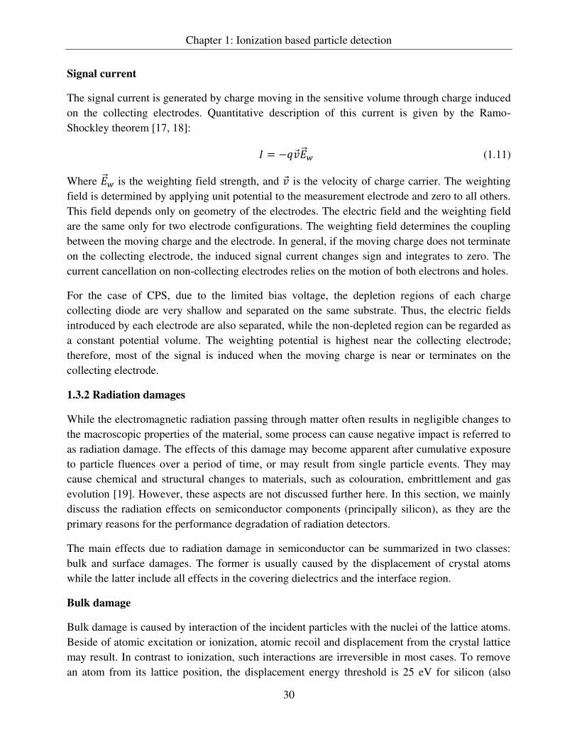
Chapter 1: Ionization based particle detection
30
Signal current
The signal current is generated by charge moving in the sensitive volume through charge induced
on the collecting electrodes. Quantitative description of this current is given by the Ramo-
Shockley theorem [17, 18]: � = − �⃗ ⃗⃗ (1.11)
Where ⃗⃗ is the weighting field strength, and �⃗ is the velocity of charge carrier. The weighting
field is determined by applying unit potential to the measurement electrode and zero to all others.
This field depends only on geometry of the electrodes. The electric field and the weighting field
are the same only for two electrode configurations. The weighting field determines the coupling
between the moving charge and the electrode. In general, if the moving charge does not terminate
on the collecting electrode, the induced signal current changes sign and integrates to zero. The
current cancellation on non-collecting electrodes relies on the motion of both electrons and holes.
For the case of CPS, due to the limited bias voltage, the depletion regions of each charge
collecting diode are very shallow and separated on the same substrate. Thus, the electric fields
introduced by each electrode are also separated, while the non-depleted region can be regarded as
a constant potential volume. The weighting potential is highest near the collecting electrode;
therefore, most of the signal is induced when the moving charge is near or terminates on the
collecting electrode.
1.3.2 Radiation damages
While the electromagnetic radiation passing through matter often results in negligible changes to
the macroscopic properties of the material, some process can cause negative impact is referred to
as radiation damage. The effects of this damage may become apparent after cumulative exposure
to particle fluences over a period of time, or may result from single particle events. They may
cause chemical and structural changes to materials, such as colouration, embrittlement and gas
evolution [19]. However, these aspects are not discussed further here. In this section, we mainly
discuss the radiation effects on semiconductor components (principally silicon), as they are the
primary reasons for the performance degradation of radiation detectors.
The main effects due to radiation damage in semiconductor can be summarized in two classes:
bulk and surface damages. The former is usually caused by the displacement of crystal atoms
while the latter include all effects in the covering dielectrics and the interface region.
Bulk damage
Bulk damage is caused by interaction of the incident particles with the nuclei of the lattice atoms.
Beside of atomic excitation or ionization, atomic recoil and displacement from the crystal lattice
may result. In contrast to ionization, such interactions are irreversible in most cases. To remove
an atom from its lattice position, the displacement energy threshold is 25 eV for silicon (also

Chapter 1: Ionization based particle detection
31
depending on incidence direction with respect to the lattice). Electrons need an energy of at least
260 keV in order to provide such energy in a collision, while protons and neutrons, because of
their higher mass, require only 190 eV. Also the ability of a particle to impart this energy is
dependent on the collision kinematics, determined by the particle mass and energy. For instance,
a 100 keV electron can transfer a maximum of ~5 eV, while a 10 MeV deuteron may transfer ~1
MeV, while the mean value transferred is generally many orders of magnitude smaller [20].
To be able to compare the damage caused by the different types of particles with different
energies, radiation damage is scaled with the non-ionizing energy loss (NIEL). The NIEL
expresses energy lost to non-ionizing events per unit length (MeV/cm or MeV cm2/g). The
equivalent fluence of 1 MeV neutrons is used as reference particles.
The defects in the crystal structure introduce additional energy levels within the semiconductor
band structure. The additional donor-like and acceptor-like energy levels can trap charge carriers,
seriously degrading the minority carrier lifetime. These additional generation-recombination
centers reduce the carrier mobility and introduce additional leakage current in a depleted
material. Due to their similar action way with donor/acceptor dopants, they also interfere with the
intended semiconductor doping. Large irradiations have even been found to cause type inversion
in high resistivity n-type silicon, producing p-type behavior [21].
Surface damage
While lattice displacement in the bulk semiconductor is due to non-ionizing energy losses, other
forms of damage may result from ionizing losses. Two examples are ionization in surface oxide
layers and the trapping of charge at interfaces. Both of these effects are caused by ionizing losses,
therefore all charged particles can contribute and the severity scales with the magnitude of the
received dose.
In silicon dioxide, an average energy of about 18 eV is required to generate an e-h pair. Most of
the charge generated in this area recombines without inducing any negative effects; however, a
small fraction of them will migrate, become trapped and accumulate at the interface.
Traps amount at the Si-Si02 interface depends on the processing parameters, such as oxidation
temperature [22]. Ionizing radiation will further increase the amount of interface traps. Trapping
centers will affect charge collection in the detector. Traps acting as generation-recombination
centers will increase recombination rate at the interface, leading to increased leakage current.
Radiation damage effects in CMOS Microelectronics
Bulk and surface damages in semiconductors are typically increasing in leakage currents,
changing in carrier concentrations and reducing in carrier lifetimes. They may show different
severity in various semiconductor devices. A summary of the effects on this study’s most concerned semiconductor device: complementary metal-oxide-semiconductor (CMOS)
technology is presented below.

Chapter 1: Ionization based particle detection
32
For silicon detectors, the bulk damage is mostly damaging to the charge collection rather than to
the readout electronics. Atom displacement in the bulk degrades minority carrier lifetime. Typical
effect is the degradation of gain and leakage current in bipolar transistor. While the operation of
MOS transistors depends on majority carriers, the bulk damage does not have much impact on
these devices. Ionizing radiation effects include single event upset (SEU), single event latch-up
(SEL), MOSFET threshold voltage shift, etc.
Charges liberated by incident high-energy ionizing particles may collect on a charge storage node
(e.g. in RAM) and be sufficient to change the binary state of the circuit. At the expense of
increased complexity, these single event upsets (SEU) may be mitigated by triple-majority voting
circuits [23].
Latch-up is an inadvertent creation of a low-impedance path, which acts as a short circuit may
lead to large current flow and device destruction [24]. In CMOS layouts, two parasitic bipolar
transistors together with the CMOS device produce a PNPN thyristor structure (Figure 1.10). A
transient current pulse from ionizing radiation may force one of the transistors into conducting
current, the second one will follow and both of them will bias each other in the positive current
feedback loop. A sustainable latch-up action can result in a high operating current which may
destroy the device due to excessive heating and metallization. The latch-up action can be
removed by powering down the circuit.
Q1Q2Rs
Rw
oxide
Rw
Rs
Q1
Q2
VDD
GND
Figure 1.10: A typical CMOS device with elements of a parasitic thyristor.
The shift of MOSFET threshold voltage (Vth) is due to hole accumulation at the gate insulation
layer [25]. As surface damage described, ionization caused holes are trapped at the Si-Si02
interface while more mobile electrons can escape into the gate circuit. The presence of this
positive charge means that a more negative gate voltage is required to obtain the same effect as
excepted. Therefore, a thin oxide layer is desired. In modern sub-micrometer processes used for

Chapter 1: Ionization based particle detection
33
integrated circuit fabrication, the gate oxide thickness is significantly reduced compare to older
technologies. As being an unwanted effect in general CMOS circuitry, this change in Vth also is
exploited in radiation dose monitoring [26].
Moreover, these accumulated positive charges may induce short circuits in the design. Shallow
surface channels can be created between different n-type regions implanted on the chip if they are
separated only by lightly doped p-type silicon. In addition, the charge accumulated at the ends of
an NMOS transistor gate with a classical rectangular shape may prevent the device from
switching off completely. Both problems can be eliminated by widely used techniques include
enclosed NMOS transistor gates and p+- type guard-rings separating n-type regions [27].
1.3.3 Single diode detectors
The ability to resolve individual particles is a desirable capability for any radiation monitor and is
essential for particle identification. This could be easily achieved in silicon sensors with a simple
p-n junction under reverse bias. The ionizing energy deposited by incident radiation within the
depletion region generates e-h pairs; these charges are separated by the electric field and
collected at the electrodes. The resulting current pulse is usually forward measured via combined
circuits, which may include charge sensitive preamplifier, pulse shaper and digitizer. This ‘pulse height analysis’ allows the total ionizing energy deposit of the event to be recorded.
A variation of the standard p-n junction diode may be created by the inclusion of a central
compensated region, where n and p-type impurities are balanced. Due to the similarities of the
compensated region with intrinsic (I) silicon, this configuration is known as a PIN diode [28].
Compare with p-n junction, larger electric field could be applied without causing an excessive
leakage current or device breakdown, due to this central compensation. Therefore, a larger
depletion region which is the sensitive volume is achieved. The reverse bias could be tens to
hundreds volts based upon applications. PIN diodes are typically 100-500 µm thick and have
surface areas of ~1 cm2. The sensor’s output observed equivalent noise charge is determined by
its capacitance which is proportional to the surface area and inversely proportional to the
depletion thickness. Additional noise is also introduced by the discrete readout circuit.
1.3.4 Pixelated detectors
One of the disadvantages of the PIN diode is its limited noise performance. Relative large diode
capacitance, large leakage current and discrete readout electronics all contribute to the large
equivalent noise (often ~1000 e- obtained in the energy deposit measurement).
A reduction in noise may be obtained by decreasing the size (and hence capacitance) of the
sensor. To maintain a useful detection volume this implies the use of pixel arrays, where each
pixel is a separate charge collection node on a single die. This segmented configuration has other
advantages: for example, allowing imaging (position reconstruction) and windowing (variation of
the total sensitive area).

Chapter 1: Ionization based particle detection
34
A number of pixel sensor architecture is available; three common varieties are Charge Coupled
Devices (CCD), hybrids and CMOS Pixel Sensors (CPS).
CCD
Charge
1
2
3
4
5
6
7
Tim
e in
clo
ck p
uls
es
Pixel 1 Pixel 2 Pixel 3
1 2 3 1 2 3 1 2 3
Charge transfer direction
Gate
SiO2
Si
Figure 1.11: Typical CCD detectors with three gates for each pixel.
The basic building block of the CCD is the MOS capacitor which is created on a silicon wafer in
arrays. An appropriate voltage applied to the poly-silicon gate changes the electrostatic potential
in the silicon and forms a potential well that collects electrons created by incident radiation. The
charge is confined in a single well by potential barriers created under neighboring gates in one
dimension and channel stopper implants in the second dimension. When a proper biasing
sequence is applied to the MOS gates, the stored charge packets can be transferred in parallel
along each column in a shift-register way (Figure 1.11). A serial shift register is located at the
bottom of the column that allows shifting samples to an output node for charge to voltage
conversion. The columns of charge may be transferred and read one at a time. For faster
applications, the entire frame of charges may be transferred to an almost identical array used for
storage.
CCDs are not only widely used in consumer electronics as visible light sensors, but also known to
be effective at collecting ionization charge from particle interactions [29]; they have been used as
particle tracking detectors [30] and investigated for use in space radiation monitors [31].
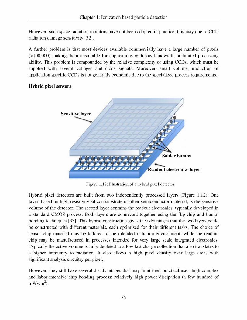
Chapter 1: Ionization based particle detection
35
However, such space radiation monitors have not been adopted in practice; this may due to CCD
radiation damage sensitivity [32].
A further problem is that most devices available commercially have a large number of pixels
(>100,000) making them unsuitable for applications with low bandwidth or limited processing
ability. This problem is compounded by the relative complexity of using CCDs, which must be
supplied with several voltages and clock signals. Moreover, small volume production of
application specific CCDs is not generally economic due to the specialized process requirements.
Hybrid pixel sensors
Sensitive layer
Readout electronics layer
Solder bumps
Figure 1.12: Illustration of a hybrid pixel detector.
Hybrid pixel detectors are built from two independently processed layers (Figure 1.12). One
layer, based on high-resistivity silicon substrate or other semiconductor material, is the sensitive
volume of the detector. The second layer contains the readout electronics, typically developed in
a standard CMOS process. Both layers are connected together using the flip-chip and bump-
bonding techniques [33]. This hybrid construction gives the advantages that the two layers could
be constructed with different materials, each optimized for their different tasks. The choice of
sensor chip material may be tailored to the intended radiation environment, while the readout
chip may be manufactured in processes intended for very large scale integrated electronics.
Typically the active volume is fully depleted to allow fast charge collection that also translates to
a higher immunity to radiation. It also allows a high pixel density over large areas with
significant analysis circuitry per pixel.
However, they still have several disadvantages that may limit their practical use: high complex
and labor-intensive chip bonding process; relatively high power dissipation (a few hundred of
mW/cm2).

Chapter 1: Ionization based particle detection
36
CMOS Pixel Sensors
CPS consist an array of pixels, each pixel contains a sensing diode which is used for collecting
the charges created by incident radiation. These collection diodes are formed by a low resistivity
p-doped silicon substrate with n-wells implanted in a thin (14-20 µm) p-type epitaxial layer.
Further processing electronics are easily integrated with the sensor part in the same substrate. A
cross section view of CPS pixel is illustrated in Figure 1.13.
Figure 1.13: Cross section view of a CPS pixel.
A major difference between the CPS with a classical detector for charged particle detection is its
active volume is not fully depleted; this is due to the limited possible sub-micro technologies
support bias voltages. Hence, the charge carriers are collected via thermal diffusion from
interactions in the epitaxial layer, instead of by a strong electric field. As described in Figure
1.13, the epitaxial layer lies between two highly doped regions: the p++ substrate and the p-well.
The doping levels of the p-well and p++ substrate are three orders of magnitude higher than the
epitaxial one, resulting in potential barriers at the region boundaries which act like mirrors and
limit the diffusion of the electrons. The charge carriers generated in the substrate will quickly
recombine and only a small fraction will reach the active layer. The liberated electrons diffuse
thermally inside the epitaxial layer and are collected by the regularly implanted n-wells.
Normally, the distance between two adjacent n-wells defines the pixel size, referred to as pitch.
The diffusing charges generated from a single incident radiation are generally shared among
several neighboring pixels, and those pixels form a cluster. Device simulations at the physical
level showed the collection time for a typical pixel pitch of 30 µm, to be less than 100 ns [16].
The current induced by the collected electrons is integrated on the n-well/p-epi junction
capacitance, resulting in a voltage drop on the collection diode, which could be processed by
further readout electronics.
CMOS Pixel Sensors have already found widespread use for various applications, ranging from
consumer electronics to visible light imaging [34] and high-energy physics [35]. These sensors

Chapter 1: Ionization based particle detection
37
are fabricated in standard CMOS VLSI technologies commonly used for modern integrated
circuit manufacturing, and are generally classified as Passive Pixel Sensors (PPS) and Active
Pixel Sensors (APS). For the case of charged particle detection, the APS structure is favorable.
Different with the PPS structure, which use just a simple selecting switch in each pixel to readout
the sensing diode integrated charge; APS integrate an additional stage of amplifier within each
pixel that makes it possible to perform several processing operations independently on each pixel
before signals are transferred to the common processing blocks. The APS are also called MAPS
(Monolithic Active Pixel Sensors) for the fact that signal sensing part and processing electronics
share the same substrate. Despite, it is a relative new approach comparing to the well-established
technologies such as CCD and hybrid detectors for charged particle detections; MAPS have
several practical advantages, including:
1. High granularity: a pixel size of 10×10 µm2 or even smaller is possible. This feature is
critical in position sensitive applications such as particle tracking. Also, for the reason that
each pixel performs as a single detector, with the same reasonable sensitive area,
pixelated sensors have more potential to cope with higher flux environment comparing to
single diode detectors;
2. A wide range of readout and digitization electronics could be integrated on the same chip
with the pixel array. These are easily fabricated in the same commercial CMOS process,
which leads to many benefits such as low cost, small size, low power consumption, high
level data information, etc.;
3. Excellent noise performance (equivalent noise charge values less than ten electrons per
pixel [36]): This is due to the low leakage current and low capacitance of the pixel diode,
which results primarily from its small size;
4. The 14-20 µm thick sensitive epitaxial layers. This gives an expected signal due to a
minimum-ionizing particle (MIP) at normal incidence of approximately 1000 electrons;
combined with its noise performance, a high signal-to-noise ratio is achievable;
5. Its sensitive layer (epitaxial layer) is underneath the readout electronics allows MAPS
having 100% fill factor which is necessary in most of particle physics applications;
6. The overall thickness may be varied in the range 50-250 µm by back-thinning the
substrate using a commercial post-processing; this allows a variable amount of material to
be present between the sensors in a telescope without affecting the sensor’s performance; 7. Good radiation tolerance (>100k Rad & 10
12neq/cm
2). Modern deep sub-micron
technologies provide intrinsic radiation hardness of MAPS; in addition, design techniques
have been developed to further increase its tolerance to radiation [37, 38].
MAPS also suffer from a few limitations. The first one is from the same feature that brings
MAPS many benefits which is the using of commercial CMOS process fabrication. The
fabrication parameters (doping profile, thickness of the epitaxial layer, etc.) are not optimized for
particle detection. The choice of industrial processes is often driven by epitaxial layer
characteristics, at the expense of the signal processing circuitry parameters (feature size, number

Chapter 1: Ionization based particle detection
38
of metal layers. Moreover, the use of PMOS transistors inside the pixel array is restricted in most
processes, thus limiting signal processing functionalities inside pixels. The second limitation
originates from the almost undepleted sensitive volume, which impacts or radiation tolerance and
charge collection speed.
1.4 Conclusion
With all these previous mentioned potential advantages, MPAS has become a promising
candidate in several radiation detection applications. One of them is space radiation monitoring.
Space radiation environment consists various species high flux (may reach several 107/cm
2/s)
particles with large energy range. Therefore, dosimeter function, particle rate meter function and
particle species identification function are all required for the detectors used in this application.
Meanwhile, on board satellite operation makes highly miniaturized, high level information
providing capability very desired features.
MAPS being monolithic full detection systems, have the potential to match all these requirements
and offer additional advantages including low power, low weight, low fabrication cost and
advanced radiation tolerance. CMOS image sensor is being used to develop a highly miniaturized
radiation monitor (HMRM) [39]. However, none investigation of MAPS dedicated designed for
this application has been made.
Therefore, the most general question for this study would be: can we design MAPS with
deposited energy measurement capability taking advantage of granularity to cope with high flux?
Previous works by the PISCEL group (Physics with Integrated CMOS Sensors and Electron
colliders) of IPHC demonstrated that MAPS reach excellent performances for charged particle
tracking in high energy physics. While, several major items differentiate tracking particles on a
ground large experiment and radiation monitoring in space.
First of all, the energy range of particles to be detected is much larger for the new application in
space. Indeed, according to NASA models [40, 41], the Earth’s radiation belt mostly consists of
protons from about 100 keV up to 400 MeV and electrons from 10 keV up to 10 MeV.
Second of all, the radiation monitor does not need to locate the particles impact but just to
separate them in order to count. The dose is then evaluated by the sum of the energy measured.
Expectation of the highest particle omnidirectional flux ranges from 103/cm
2/s to several
107/cm
2/s.
Finally, contrary to ground experiment where large signal treatment power can be available aside
the sensor, an instrument on board a satellite shall provide high level information by itself.
The challenge of this thesis is to demonstrate both the sensitivity of CPS to the expected
radiations and the ability to integrate directly on the chip the data processing which turns the
sensor into a really autonomous dosimeter.

Chapter 1: Ionization based particle detection
39
Bibliography
[1] H. Bethe. Zur theorie des durchgangs schneller korpuskularstrahlen durch materie. Ann. Physik,
397:325─400, 1930.
[2] H. A. Bethe. Molière's theory of multiple scattering. Phys. Rev., 89:1256─1266, 1953.
[3] N. J. Carron. An introduction to the passage of energetic particles through matter. Taylor and
Francis, 2006.
[4] J. Beringer et al. (Particle Data Group). Review of particle physics. Phys. Rev. D, 86:010001,
2012.
[5] M. J. Berger et al. ESTAR: Electron stopping power and range. National Institute of Standards
and Technology, http://physics.nist.gov/PhysRefData/Star/Text/ESTAR.html.
[6] Glenn F. Knoll. Radiation detection and measurement. Second edition. 1989.
[7] National Institute of Standards and Technology, Physical Means. Laboratory. Stopping- power
and range tables for protons/electrons.
http://physics.nist.gov/PhysRefData/Star/Text/PSTAR.html
[8] W. H. Barkas et al. Mass-ratio method applied to the measurement of l-meson masses and the
energy balance in pion decay. Phys. Rev., 101:778, 1956.
[9] F. Bloch. Zur bremsung rasch bewegter teilchen beim durchgang durch materie. Ann. Physik,
408:285─320, 1933.
[10] J. F. Ziegler. Stopping of energetic light ions in elemental matter. J. appl. phys., 85:1249─1272,
1999.
[11] L. Landau, On the energy loss of fast particles by ionization, J. Phs. (USSR), vol. 8, p. 201, 1994.
[12] K. Nakamura et al., Particle Data Group: Review of Particle Physics, J. Phys. G, vol. 37, 2010.
[13] G. Hall. Ionisation energy losses of highly relativistic charged particles in thin silicon layers.
Nucl. Instrum. Methods, 220:356─362, 1984.
[14] Walter D. Loveland et al. Modern nuclear chemistry. 2006
[15] M. S. Tyagi, Introduction of Semiconductor Materials and Devices, John Wiley & Sons, 1991
[16] G. Deptuch. New generation of monolithic active pixel sensors for charged particle detection,
Ph.D. dissertation, Université Louis Pasteur, Strasbourg, France, 2002.
[17] W. Shockley. Currents to conductors induced by a moving point charge. Journal of Applied
Physics, vol. 9, no. 10, pp. 635─636, 1938.
[18] S. Ramo. Currents induced by electron motion. Proceedings of the IRE, vol. 27 no. 9, pp.
584─585, sept.1939.
[19] M. W. Thompson. Defects and radiation damage in metals. Cambridge University Press. 1969

Chapter 1: Ionization based particle detection
40
[20] J. W. Corbett. Electron radiation damage in semiconductors and metals. Academic Press, 1966.
[21] Pitzl, D et al. Type inversion in silicon detectors. Nuclear Instruments and Methods in Physics
Research Section A, Volume 311, Issue 1-2, p. 98─104.
[22] L. Do Thanh et al. Elimination and Generation of Si-SiO2 interface traps by low temperature
hydrogen annealing. Journal of the Electrochemical Society. 1988
[23] L. Rossi et al. Pixel detectors from fundamentals to applications. Springer, 2006
[24] H. L. Hughes and J. M. Benedetto. Radiation effects and hardening of MOS technology: devices
and circuits. IEEE Trans. Nuc. Sci., 50:500─521, 2003.
[25] G. Lutz. Semiconductor radiation detectors. Springer, 1999
[26] S-J. Kim et al. Use of a MOSFET for radiation monitoring in space and comparison with the
NASA trapped particle model. J. Korean Phy. Soc., 48:865─869, 2006
[27] G. Anelli et al. Radiation tolerant VLSI circuits in standard deep submicron CMOS technologies
for the LHC experiments: Practical design aspects. IEEE Trans. Nuc. Sci., 46:1690─1696, 1999
[28] B. Doherty. PIN Diode Fundamentals. Watertown, MA: Microsemi Corp., MicroNote Series
701.
[29] T. S. Lomheim et al. Imaging charge-couple device (CCD) transient response to 17 and 50
MeV proton and heavy-ion irradiation. IEEE Trans. Nuc. Sci., 37:1876-1885, 1990.
[30] S. Watts. Ccd vertex detectors. Nucl. Instrum. Methods Phys. Res., Sect. A, vol. 265, pp. 99-104,
1988.
[31] A. M. Chugg et al. A CCD miniature radiation monitor. IEEE Trans. Nuc. Sci., 49:1327-1332,
2002.
[32] J. Janesick. Scientific Charge-Coupled Devices. Washington, USA: SPIE- The International
Society for Optical Engineering, 2001.
[33] M. Caccia. The challenge of hybridization. Nucl. Instrum. Methods Phys. Res., Sect. A, vol. 465,
pp. 195-199, 2001.
[34] S. Mendis et al. CMOS active pixel image sensor. IEEE Trans. Electron. Dev., 41:452-453,
1994.
[35] S. Heini et al. A MOS Current-Mode Active Pixel Sensor for High Energy Physics and
Biomedical Imaging Applications. IEEE Trans. Nuc. Sci. vol.56, pp.346-353, 2009.
[36] R. E. Coath et al. A low noise pixel architecture for scientific CMOS monolithic active pixel
sensors. IEEE Trans. Nuc. Sci., 57:2490-2496, 2010.
[37] W. Dulinski et al. Radiation hardness study of an APS CMOS particle tracker. In IEEE Nucl. Sci.
Conf. R., volume 1, pages 100-103, 2001.

Chapter 1: Ionization based particle detection
41
[38] E. S. Eid et al. Design and characterization of ionizing radiation-tolerant CMOS APS image
sensors up to 30 Mrd (Si) total dose. IEEE Trans. Nuc. Sci., 48:1796-1806, 2001.
[39] N. Guerrini et al. Design and characterization of a highly miniaturized radiation monitor HMRM.
nucl. Instrum. Methods Phys. Res., Sect. A, vol. 731, pp. 154-159, 2013.
[40] D.M.Sawyer and J. I. Vette, AP-8 trapped proton environment for solar maximum and solar
minimum, 1976 NASA TM-X-72605.
[41] J. I. Vette, The AE-8 trapped electron model environment, 1991 NSSDC/WDC-A-R&S 91-24.

42
Chapter 2
MAPS for particle tracking detection
MAPS used for high energy charged particle tracking have been significantly developed over the
past more than a dozen years. To meet with the increasing need of high performance flavor
tagging capabilities in particle physics experiments, in 1999, the IReS-LEPSI group proposed the
idea of using MAPS devices for high-energy charged particle tracking [1, 2]. Since that time, the
ability of the monolithic CMOS pixel sensors to provide charged particle tracking has been
demonstrated in a series of MIMOSA (Minimum Ionizing particle MOS Active pixel sensor)
prototypes.
This thesis was extended from the state-of-the-art CPS development performed by the CMOS
research group at IPHC. The following sections describe the development specifications for
particle tracking detection; the optimizations of MAPS to meet these contradictory requirements;
the the design and performances of MIMOSA 26 which is the first full scale CMOS sensor with
high read-out speed and integrated zero suppression [3]; and finally, based on these discussions,
conclude this chapter with the proposed MAPS architecture for the new application: space
radiation monitoring.
2.1 Specifications for particle tracking
Subatomic physics experiments express a growing need for very high performance flavor tagging
with emphasis on short lived particles (e.g. charmed mesons) through their decay vertex. This
calls for an excellent vertexing and tracking system in order to reconstruct displaced vertices and
to measure precisely track momenta. The specifications for sensor design optimization are
imposed both from the physics goals of the experiment and its running environment. It is a huge
challenge for sensor design to meet all these requirements, since they often conflict with each
other. For instance, the very high single point resolution implies a highly segmented sensor. This
comes in contradiction with the rather fast readout speed, imposed by the beam induced
Chapter 2: MAPS for particle tracking detection
43
background. Moreover, the big number of columns of a highly segmented sensor increased the
power consumption, which may translate in a complex cooling system or degraded sensor
performance. In this section, we are going to explain these trade-offs.
2.1.1 Physics goals Driven Specifications
Those short lived particles firstly fly over distances as short as a few hundred micrometers from
the interaction point and they decay into secondary more stable particles, which can be detected
in the vertex detector. An out standing spatial resolution in the order of several micrometers,
provided by a high precision vertex detector, is required for reconstructing the decay vertex from
these particles.
Granularity
The spatial resolution is in fact equivalent to the error on the real hit position, it delivered by a
detector mostly on the geometry of the detector segments. Therefore, the most critical parameter
is the pitch of pixels. In order to optimize the spatial resolution performance, the sensor has to
target with fine granularity. For tracks that are randomly spread, differences between the true
positions and the measured ones have a Gaussian distribution with the standard deviation � given
by � = ∫ � =⁄− ⁄ (2.1)
where is the segment pitch size in a given direction. Simply considering the seed pixel, the hit
position resolution is defined by the segment pitch divided by √ . For a pixel size of 30 µm ×
30 µm, the resolution theoretically reaches about 8.5 µm.
This value can be further decreased to a few micrometers by using of center-of-gravity or �
algorithms which are taking advantage of charge sharing between neighboring segments that
form clusters [4]. An analogue sensor is mandatory to perform these algorithms.
Thickness
The spatial resolution has to be complemented by a very light and thin material budget, ensuring
that particles traversing the detector will only be slightly affected by multiple scattering, which
affects the direction of particles thus fooling the reconstruction of their trajectory and their spatial
origin. CMOS pixel sensors can be thinned to a few tens of µm without affecting the performance
which is a particularly attractive advantage comparing with other pixelated sensors.
2.1.2 Environment Driven Specifications
Vertex reconstruction is performed by extrapolating tracks measured by different layers of
sensors. In order to get the shortest extrapolation length, the vertex detector is always as close as
possible to the particle collision interaction point (several centimeters in general). Being the inner

Chapter 2: MAPS for particle tracking detection
44
most layer, the running environment of vertex detector also brings some constraints, which paly a
major role on the detector design.
Radiation Tolerance
Obviously, the innermost layer of the detector will be subject to the biggest rate of radiation
background, thus suffers from severe radiation damage. For instance, the high center-of-mass
energy of the future ILC (International Linear Collider) will be as high as 500 GeV. For 3 years
operation, the radiation hardness requirements are ~150 kRad for ionising radiation and ≤ 2×10¹¹
neq/cm2 for the non-ionising radiation [5].
Speed
A very high readout speed is required in order to avoid the problem of pile up, appearing when
two or more particles simultaneously touch the same area of the detector. Obviously, the solution
of the problem is to increase the readout speed: to take away the information as fast as possible,
so that the probability of pile up reduces.
Cooling System & Power dissipation
The performances of detectors’ readout electronics will be degraded by the increasing of
operation temperature which is coming from its own power dissipation. To keep detectors a
stable performance, cooling system or very low power dissipation is required.
However, cooling system for vertex detector is a crucial element of the design, since it is
introducing additional material which would increase the multiple scattering along particle path.
Being located outside the detector volume does not affect its performance, but may impact the
outer tracking performances and the particle flow analysis. Therefore, no extremely sophisticated
cooling system is allowed.
There are two methods to keep low power dissipation. One way is control the time structure of
the particles beam, so the sensors can be switched off between power cycling. The other way is
just keep the power consumption of the sensor itself as low as possible.
2.2 MAPS technology
In summary, the physics goals and running conditions call for sensor technologies that offer a
high granularity, low material budget, low power dissipation, high readout speed and moderate
radiation tolerance. Currently, no present technology can satisfy all the above requirements
perfectly. As previously described (Chapter 1, section 1.3.4), all the practical advantages make
MAPS a very promising technology for this application. Over the past years, tremendous efforts
have been made by the PIXEL group in IPHC to optimize MAPS for all the requirements through
a series of MIMOSA prototypes, significant improvements have been obtained [6].

Chapter 2: MAPS for particle tracking detection
45
2.2.1 Global architecture and fast readout strategy
With the same granularity, analogue sensor allows for a finer spatial resolution than the one
expected from binary positioning algorithm. However, analogue data output is relatively slow,
and expect a high data flow that may set severe requirements on the Data Acquisition (DAQ)
system. With the concern of speed and release the stress on DAQ system, the data sparsification
should take place as close as possible to the sensing pixels arrays. One approach could be
integrating the whole data sparsification functionalities inside the pixel. This could reduce the
non-sensitive area, so material budget of the detector; while, the complex signal processing will
lead to the increase of pixel pitch size, thus degrading the single point resolution. A viable
solution is to increase the readout speed of the pixels arrays and integrate the data sparsification
logic on the periphery of the sensor.
Digitization stage
-
Pixel matrix
Memory + output
Row sel
0 suppression stage
Figure 2.1: Column parallel readout principle [7].
It takes only ~ 100 ns for the charge collection by diffusion in a pixel with an un-depleted
epitaxial layer. Therefore, the time resolution of MAPS is limited by the time needed to obtain
the information from all the pixels of the sensor as well as the pixel occupancy.
In order to increase the readout speed without sacrifice too much power consumption; column
parallel readout (called rolling shutter as well) mode is a viable solution for the readout of the
MAPS. As illustrated in Fig. 2.1, pixels are addressing sequentially row by row, the output of
pixels in one column are multiplexed in a single bus. Pixels in a same row are reading
simultaneously to reduce the time needed for reading the whole matrix; each time, only a single
row of pixels are working, other pixels are switched off to save the power. The sparsification is

Chapter 2: MAPS for particle tracking detection
46
provided by discriminators, located at the bottom of each column and being common for all the
pixels of a column.
For a real size sensor (~ 106 pixels, ~ 1000 rows and ~1000 columns), working in a high speed
(~10 k frames/s), the data flow (~10 Gbits/s) provided by discriminators is a great challenge for
transmission which also leads to more complex electronics and higher power dissipation. The
best option would be to integrate a zero suppression block on the sensor itself. The data
suppression level (between 10 and 1000) depends on the pixel occupancy.
2.2.2 Basic pixel architectures
Pixel is the sensitive part of MAPS, it could directly affect the performances of the detector, for
instance radiation tolerance, detection efficiency, fake hit rate, etc. For radiation tolerance
optimization, many different diode layouts were tested to minimize the dark current and its
increase due to radiation, various CMOS technologies with different epitaxial layer thickness and
resistivity have been tried [8]. High detection efficiency (close to 100%) and low fake hit rate
(close to 0) are both key parameters to ensure an accurate tracking performance, besides high
granularity. However, it is always a trade-off between efficiency and fake hit rate which are
determined by the applied threshold on the signal-to-noise ratio (SNR). A high SNR value is
essential for high efficiency and low fake hit rate in the same time.
ResetCharge
collection
Vdiode
t0 t1 t2
t0 t1 t2
Vsig
VddaVdiode
GND
Charge
sensing
diode
ResetM1
M2
M3
Row_SEL
COL_bus
(a) (b)
Figure 2.2: The classical single pixel cell: (a) schematic, (b) timing diagram showing the operation and the
signal shape.
The basic single pixel readout architecture, consisting of three transistors and the charge sensing
diode [9], is schematically presented in Fig. 2.2 (a). The transistor M1 resets the diode to the
reverse bias, and the transistor M2 operates as a source follower connected to a row selection

Chapter 2: MAPS for particle tracking detection
47
switch (M3). The charge is integrated within the time separated by two consecutive reset
operations and observed as a voltage drop on the floating n-well/p-substrate diode. The current
source for the source follower (SF) is placed outside the pixel. The leakage current (several fA at
room temperature) leads to a signal offset which depends strongly on the integration time. This
offset is referred to as pedestal, and varies from pixel to pixel due to the dispersion of process
parameters. In applications with high signal intensity or large signals, this reset structure would
ensure the diode recover quickly and completely for the following incident.
Another pixel architecture (Fig. 2.3), based on the two diodes reversely connected together, was
proposed for application of low signal intensity and small signals [10]. The charge sensing diode
(D1) is also reverse biased as in the reset structure, while the load diode (D2) is forward biased.
When the reverse biased diode D1 collects charge, the voltage on the diode drops and a slow
discharging begins. The discharge time constant is defined by the equivalent resistance of the
forward biased diode D2 and the capacitance of the diode D1. This structure is often referred to as
a self-biased (SB) pixel. Compared to the reset structure, this SB pixel is free from reset noise
and signal offset.
VddaVdiode
GND
Charge
sensing
diode
M2
M3
Row_SEL
COL_bus
D1
D2
Vdiode
t0 t1
Vsig
Charge
collection
(a) (b)
Figure 2.3: Self-biased pixel cell: (a) schematic, (b) timing diagram showing the operation and the signal
shape.
As aforementioned, the amount of charge generated by a normal impinging MIP for typical
epitaxial thickness is ~1000 e-. Since the charges are expected to be shared between neighboring
pixels, the amount of charge collected by a single diode is usually only a few hundreds of
electrons. In both these two structure, the voltage signal generated on the charge sensing diode,
typically being of the order of several mV, is then readout by a source follower with a gain factor
about 0.7-0.8. Such a weak signal can be easily affected by the electronic noise. Thus the signal
amplification in each pixel is necessary to minimize the noise contribution of the readout chain
and to increase the readout flexibility as well as on-chip processing capabilities. Different in-
pixel amplifier architectures have been studied and implemented in many MIMOSA prototypes,

Chapter 2: MAPS for particle tracking detection
48
and the detailed descriptions can be found in [11]. A further optimization of in-pixel amplifiers
are addressed in [12].
2.2.3 Sources of Noise in MAPS
The origins of the noise in a CMOS sensor can be generally divided in 2 main categories, the
Fixed Pattern Noise (FPN) and the Temporal Noise (TN).
2.2.3.1 Fixed Pattern Noise (FPN)
Inside the pixels matrix, the sensing diode output voltage pedestal varies from one pixel to
another. FPN is defined as the standard deviation of the pedestal distribution. In order to measure
the signal, FPN needs to be subtracted from the pixel’s response. It originates from mask production mismatches, doping concentration variations, or a contamination during the CMOS
fabrication processes.
2.2.3.2 Temporal Noise (TN)
When the pixel’s input is constant, the temporal fluctuation of its output is described as temporal
noise. For MAPS used in MIP detection, due to the signal is low (several mV on the diode), the
temporal noise can significantly influence the SNR, thus influence the sensor performance. Its
main sources are shot noise, thermal noise and 1/f (flicker) noise.
The shot noise is originates from the discrete nature of electric charge. In electronic circuits, the
current flow is not continuous but randomly fluctuates. At the microscopic level, the
unpredictable variation of the current is called shot noise.
The thermal noise is the electronic noise generated by the thermal agitation of the charge carriers
(usually the electrons) inside an electrical conductor at equilibrium, which happens regardless of
any applied voltage. The thermal noise is approximately a white noise; its power spectral density
is nearly constant throughout the frequency spectrum. When limited to a finite bandwidth, it has a
nearly Gaussian amplitude distribution.
The 1/f noise is a type of electronic noise (also called flicker noise) featuring a power spectral
density inversely proportional to the frequency. It occurs in almost all electronic devices. In the
CMOS sensors, it is originating predominantly form MOS transistors.
The analysis of TN is quite complicate in real sensors, since the noise is not stationary and the
circuit is not time invariant. A complete and rigorous analysis can be found in [13]. For the
purpose of this thesis, the noise sources in the basic reset pixel structure (Fig. 2.2) are analyzed
for each operation phase.
Noise during the reset phase: during the reset phase, the gate of the reset transistor M1 is set to
the potential of the power supply; M1 starts to conduct the current to restore the charges on the
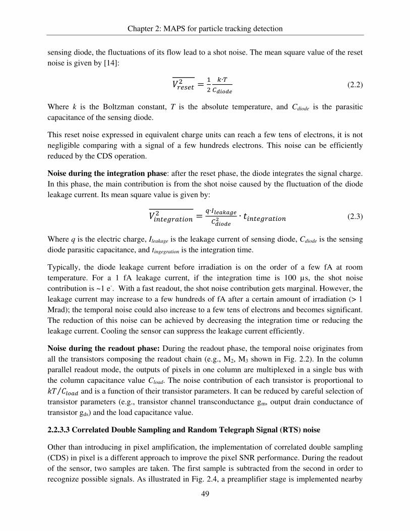
Chapter 2: MAPS for particle tracking detection
49
sensing diode, the fluctuations of its flow lead to a shot noise. The mean square value of the reset
noise is given by [14]: = ∙ (2.2)
Where k is the Boltzman constant, T is the absolute temperature, and Cdiode is the parasitic
capacitance of the sensing diode.
This reset noise expressed in equivalent charge units can reach a few tens of electrons, it is not
negligible comparing with a signal of a few hundreds electrons. This noise can be efficiently
reduced by the CDS operation.
Noise during the integration phase: after the reset phase, the diode integrates the signal charge.
In this phase, the main contribution is from the shot noise caused by the fluctuation of the diode
leakage current. Its mean square value is given by: = ∙ ∙ (2.3)
Where q is the electric charge, Ileakage is the leakage current of sensing diode, Cdiode is the sensing
diode parasitic capacitance, and tingegration is the integration time.
Typically, the diode leakage current before irradiation is on the order of a few fA at room
temperature. For a 1 fA leakage current, if the integration time is 100 µs, the shot noise
contribution is ~1 e-. With a fast readout, the shot noise contribution gets marginal. However, the
leakage current may increase to a few hundreds of fA after a certain amount of irradiation (> 1
Mrad); the temporal noise could also increase to a few tens of electrons and becomes significant.
The reduction of this noise can be achieved by decreasing the integration time or reducing the
leakage current. Cooling the sensor can suppress the leakage current efficiently.
Noise during the readout phase: During the readout phase, the temporal noise originates from
all the transistors composing the readout chain (e.g., M2, M3 shown in Fig. 2.2). In the column
parallel readout mode, the outputs of pixels in one column are multiplexed in a single bus with
the column capacitance value Cload. The noise contribution of each transistor is proportional to ⁄ and is a function of their transistor parameters. It can be reduced by careful selection of
transistor parameters (e.g., transistor channel transconductance gm, output drain conductance of
transistor gds) and the load capacitance value.
2.2.3.3 Correlated Double Sampling and Random Telegraph Signal (RTS) noise
Other than introducing in pixel amplification, the implementation of correlated double sampling
(CDS) in pixel is a different approach to improve the pixel SNR performance. During the readout
of the sensor, two samples are taken. The first sample is subtracted from the second in order to
recognize possible signals. As illustrated in Fig. 2.4, a preamplifier stage is implemented nearby

Chapter 2: MAPS for particle tracking detection
50
the sensing diode. It is active only when the row is selected to be read which reduces the power
consumption. A serially connected capacitor and a clamping switch are used for the double
sampling. A source follower and a row select switch are employed to output the signal. Another
group switch is used for large pixel arrays (~ 2×2 cm2) to reduce the column line capacitance thus
to increase the readout speed. RD and CALIB are column-level commands and are used to
memorize the output signal level and the reference level of the pixel output stage. This double
sampling operation eliminates the FPN and reset noise which has a large contribution to TN; it
also reduces rejects most of the flicker noise (1/f). The in-pixel amplifiers combined with in-pixel
CDS circuitry are commonly used in the MIMOSA prototypes after MIMOSA-6.
Figure 2.4: Pixel topology with in pixel amplification and CDS.
With RTSCurrent
TimeCurrent
Timet1 t2
Without RTS
Difference
between two
sampling
Figure 2.5: Illustration of Random Telegraph Signal (RTS).
R D C A L IB
C h a rg e
s e n s in g
e le m e n t
R S T (o p tio n a l)
A M P S F
S lc t R o w
P W R O N
C la m p in g
S lc t G rp

Chapter 2: MAPS for particle tracking detection
51
However, for MPAS used in MIP detection or other low signal sensitivity applications, this noise
reduction brings another issue which is the RTS noise. The current fluctuation phenomenon is
seen in small area devices, such as the sensing diode leakage current and drain current of the
transistor (gate area <1 µm2) in CMOS sensor. As illustrated in Fig. 2.5, the multi-bistable
current waveform on the top of the figure is known as RTS noise. It originates from individual
traps in the oxide near Si/SiO2 interface. The times t1 and t2 correspond to the time when the two
samples required for the CDS operation are taken. In the case of RTS, the CDS operation may
result in a signal equal to the difference between two current levels which could be recognized as
a signal generated by an impinging particle.
The feature of RTS noise impact on the sensor output noise spatial distribution is shown in Fig.
2.6. It has a non-gaussian shape with a positive skew which means a big number of “quiet pixels” with a small number of “noisy pixels”. This positive skew comes from the significant RTS noise of the in-pixel source follower impacting on the sensor output noise response. The sensor’s RTS performance is strongly dependent on the process quality and characteristics such as: biasing,
readout architecture, operation speed, temperature, radiation species and radiation levels. For a
given process conditions the main parameter for improving the array RTS noise non uniformity is
the channel length of the source follower [16].
POSITIVE SKEW
Pixel output noise distribution (rms)
Pix
el n
um
ber
Figure 2.6: Pixel output noise distribution at the sensor output [15].
2.3 MIMOSA 26
MIMOSA 26 (block diagram shows in Fig. 2.7) is the first full scale digital sensor of the
MIMOSA series with integrated signal processing. It adapts the optimal pixel design of
MIMOSA 22 / 22bis [17, 18] combined with the zero suppression chip SUZE-02 [19], that
performs on line data sparsification. Fabricated in the AMS 0.35 µm technology, it consists of
576 rows and 1152 columns with 18.4 µm pixel pitch size; resulting in a sensitive area of ~ 224
Chapter 2: MAPS for particle tracking detection
52
mm2 and better than 4 µm single point resolution. The signal is amplified by a pre-amplification
stage and undergoes the Correlated Double Sampling (CDS) in pixel, and then to be digitized
using column level discriminators. Finally, the output is pipelined to the zero suppression circuit
integrated on the chip. This architecture allows a fast readout frequency of ~10 k frames/s.
Figure 2.7: MIMOSA 26 block diagram.
2.3.1 Pixel
The pixel schematic of MIMOSA 26 is illustrated in Fig. 2.8. Its sensitive part is using the self-
biased architecture. The amplification stage nearby the sensing diode is based on a common
source (CS) amplifier (M3 and M2); an extra transistor M4 is used to increase the AC gain of the
amplifier (detailed described in [20]) and a negative low frequency feedback (through M5) was
introduced to decrease the operation point variation due to process dispersion as well as biasing
the sensing diodes [21]. MOS capacitor M7 and M8 work as a low-pass filter and the serially
connected capacitor for CDS. M10 is the source follower and its current source is in the column.
M1, M6, M9, M11 and M12 are switches.
In order to enhance the pixel radiation tolerance, the feedback transistor M5 was designed as an
enclosed layout transistor (ELT) surrounded by a guard ring which could minimize the grain-
source leakage current; the thick oxide surrounding the sensing diode by default was replaced by
thin oxide (gate oxide ring). The improved performance of this radiation tolerant design is
reported in [22].
For a single pixel, the activated power consumption is about 200 µW; Charge-to-Voltage
conversion Factor (CVF) is 55.8. Its measured temporal noise is 12.3 e- before radiation and
increasing to 21 e- with 300 kRad irradiation dose; while the fixed pattern noise keeps at ~ 4 e-
with the irradiation lower than 300 kRad.

Chapter 2: MAPS for particle tracking detection
53
Figure 2.8: Pixel schematic of MIMOSA 26.
2.3.2 Analogue to Digital Conversion
The analogue to digital convertor (ADC) is implemented identically for each column below the
pixel array. Its number of bits is mainly determined by the required spatial resolution. More
number of bits leads to higher spatial resolution while sacrifices larger layout area and power
dissipation. For the case of MIMOSA 26, 1 bit ADC which is just a comparator is employed to
ensure a 4 µm spatial resolution. The conversion time of the comparator matches with the pixel
readout speed, so the signals transmitted from pixel array row by row could be converted to
digital data continuously.
G0 G1
Vref1
Vref2
Figure 2.9: Architecture of the column-level discriminator.
Considering the small amplitude of the analogue signal, it is mandatory to use an offset
compensated amplifying stage which corrects the residual offsets. As it is shown in Fig. 2.9, the
architecture of the comparator is based on an auto-zeroed amplifying stage and a dynamic latch.
The discriminator subtracts VRD from VCALIB (the in-pixel double sampling voltages) and
compares it with a threshold value. All the 1152 column level discriminators will use a common

Chapter 2: MAPS for particle tracking detection
54
threshold value for comparisons. This value is adjusted by the difference of two programmable
references Vref1 and Vref2 and with the purpose of ensuring ~ 100% of detection efficiency and
low fake hit rate (~ 10-4
– 10-5
). The design detail is described in [23].
The comparator features compact layout, low power consumption and low noise performances.
The layout of this comparator is fitted in the pixel pitch (18.4 µm); its power consumption is
below 250 µW; and the noise extracted from “S-curves” amount to 0.3 mV and 0.2 mV for temporal noise and the FPN respectively.
2.3.3 Zero suppression
With the 10 kFrames/s working speed, for MIMOSA 26, the data flow provided by the column-
level discriminators reaches up to 6.5 Gb/s per chip. In order to better handle this high data flow,
and relax the requirements of the DAQ, The zero suppression circuitry was located right after the
discriminators. It takes the output of the discriminators as input and searches for fired pixels row
by row; it skips non hit pixels and identifies contiguous pixels (string) having their signals above
the threshold. The sparse data scan logic is based on a Priority Look Ahead (PLA) algorithm
which can be found in [24]. The length and addresses of the strings beginning are stored in one of
the two SRAM allowing a continuous readout. The possible data compression factor is ranging
from 10 to 1000, depending on the hit density per frame. The sparsified data of each frame after
zero suppression is then sent out during the acquisition of the next frame via LVDS transmitters.
2.3.4 Performances
The first MIMOSA 26 prototypes arrived from the foundry in February 2009. The sensor was
extensively tested in the laboratory and with a high-energy (120 GeV) pion beam. It measured a
temporal noise ~12 – 13 e-
with 80 MHz clock operation frequency. It exhibited a detection
efficiency of ~ 99.5% for a fake hit rate ≤ − per pixel and a spatial resolution of ~ 3.5 µm.
Other achieved performance parameters are summarized in Table 2.1.
Table 2.1: Performance of MIMOSA 26.
Sensor external dimensions 21.2×10.6 µm2
Number of pixels ~660 000
Readout time ≤ 100 µs
Power consumption ~300 mW/cm2
Non-ionizing radiation tolerance Few 1012
neq/cm2
Ionizing radiation tolerance ~300 kRad
Pixel pitch ~3 µm
Material budget per sensor 0.05 %X0

Chapter 2: MAPS for particle tracking detection
55
2.4 Conclusions
The excellent performances of CPS for charged particle tracking in high energy physics have
been demonstrated. However, the sensors designed for particle tracking is not suitable to be
directly used in space radiation monitoring. Due to the differences of tracking particles on a
ground large experiment and radiation monitoring in space, the sensor design strategy for each
electronic part may be different.
Firstly, for these two applications the goals of the analogue processing parts are different,
because of their different input energy range. In particle tracking application, the target particles
are MIPs, that fact makes the analogue processing mainly focus on pursuing a high gain and low
noise. In space radiation environment, the energy range of particles to be detected is much larger;
their deposited energy in the detector may range several orders of magnitude. In order to realize
the dosimeter function, the analogue processing needs to trade off between gain and large signal
saturation. Also, larger input signals combined with a high flux density, the sensing diode used
for space radiation needs more attention on fast and complete recovery from large input signals.
Further more, a relative linear response is also required for the following more than one bit
digitization.
Secondly, a more than one bit digitization is needed for space application. The radiation monitor
does not need to locate the particles impact but just to separate them in order to count. The dose
is evaluated by the sum of the energy measured. To provide more precisely the particle deposited
energy information, an ADC instead of a discriminator is necessary.
Finally, the required embedded digital processing functions are totally different. For particle
tracking, zero suppression function is employed to relax the data transmission stress as well as
the requirement for DAQ. With the same consideration, and even more, an instrument on board a
satellite does not have large signal treatment power available aside the sensor. The embedded
algorithm for space application should not only suppress the data amount but also processing the
data and provide high level information.
Therefore, generally, an analogue processing circuit with moderate gain, relative linear response
to a large input dynamic range; a more than one bit ADC; and an embedded digital processing
block with suitable algorithm are desired for the CPS used for space radiation monitoring
application. More precisely specifications could only be determined through carefully application
study and physical simulations which are described in Chapter 3.

Chapter 2: MAPS for particle tracking detection
56
Bibliography
[1] M. Winter et al., The Fourth Workshop of the 2nd
Joint ECFA/DESY Study on Physics and
Detectors for a Linear Electron-Positron Collider, Oxford, March 1999.
[2] Y. Gornushkin et al., Test results of monolithic active pixel sensors for charged particle
tracking. Nucl. Instrum. Methods Phys. Res., Sect. A, vol. 478, pp. 311-315.
[3] HU-GUO C et al., First reticule size MPAS with digital output and integrated zero suppression for
the EUDET-JRA1 beam telescope. Nucl. Instrum. Methods Phys. Res., Sect. A, vol. 623, pp. 480-
482.
[4] D. Contarato, Silicon Detectors for Particle Tracking at Future High-Energy Physics Experiments.
PhD thesis, University Hamburg, Hamburg, 2005.
[5] A. Besson et al., A vertex detector for the international linear collider based on CMOS sensors.
Nucl. Instrum. Methods Phys. Res., Sect., vol. 568, pp. 233-239.
[6] W. Dulinski et al., Optimization of tracking performance of CMOS monolithic active pixel
sensors. Nucl. Instrum. Methods Phys. Res., Sect. A, vol. 513, pp. 291-295, 2003.
[7] J. Baudot. Future of Low Mass Pixel Systems with MAPS, 19th International Workshop on Vertex
Detectors. Loch Lomond, Scotland, UK, June 6-11 2010.
[8] M. Koziel. Development of radiation hardened pixel sensors for charged particle detection. Ph.D.
dissertation, Université de Strasbourg, France, 2012.
[9] R. Turchetta et al., A monolithic active pixel sensor for charged particle tracking and imaging
using standard VLSI CMOS technology. Nucl. Instrum. Methods Phys. Res., Sect. A, vol. 458, pp.
677-689.
[10] G. Deptuch. New generation of monolithic active pixel sensors for charged particle detection.
Ph.D. dissertation, Université Louis Pasteur, Strasbourg, France, 2002.
[11] M. Szelezniak. Development of pixel detectors with integrated microcircuits for the vertex
detector in the STAR experiment at the RHIC collider. Ph.D. dissertation, Université Louis
Pasteur, Strasbourg, France, 2008.
[12] A. Dorokhov. Optimization of amplifiers for monolithic active pixel sensors. In topical workshop
on Electronics for Particle Physics, Prague, Czech Republic, Sep. 2007, pp. 423-427.
[13] H. Tian. Noise analysis in CMOS image sensors. Ph.D. thesis, Standford University, USA. 2000.
[14] H. Tian et al., Analysis of temporal noise in CMOS photodiode active pixel sensor. IEEE
transactions on Electron Devices, 36:92-101, 2001.

Chapter 2: MAPS for particle tracking detection
57
[15] P. Martin-Gonthier et al,. Low-Frequency Noise Impact on CMOS Image Sensors. 24th
conference on design of circuit and integrated systems, DCIS’09, 18-20 Nov 2009, Zaragoza,
Span.
[16] A. Lahav et al., Optimization of Random Telegraph Noise Non Uniformity in a CMOS Pixel
with a pinned-photodiode. International Image Sensor Workshop, pp. 219-223, June 2007.
[17] A. Dorokhov et al., Optimization of amplifiers for monolithic active pixel sensors for the STAR
detector, IEEE Nuc. Sci. Symp. Conf., October 2008, Dresden, Germany, 2008.
[18] M. Gelin et al., Intermediate digital chip sensor for the EUDET-JRA1 beam tetescope, IEEE
Nucl. Sci. Symp. Conf. Record, October 2008, Dresden, Germany, 2008.
[19] A. Himmi et al., SUZE: Zero suppression micro-circuit,
http://www.eudet.org/e26/e28/e182/e591/eudet-memo-2007-55.pdf .
[20] A. Dorokhov. NMOS-based high gain amplifier for MAPS. VIth International Meeting on Front
End Electronics, Perugia, Italy, May 17-20 2006.
[21] A. Dorokhov et al., Optimization of amplifiers for monolithic active pixel sensors. TWEPP 2007,
Prague, Czech Republic, September 3-7, 2007.
[22] W. Dulinski et al. Development of CMOS Sensors for Future High Precision Position Sensitive
Detecotrs. VCI 2007, Vienna, Austria, February 19-24 2007.
[23] Y. Degerli et al., A fast monolithic active pixel sensor with pixel-level reset noise suppression
and binary outputs for charged particle detection. IEEE Trans. Nucl. Sci. 52 (2005) 3186.
[24] A. Himmi. A zero suppression Micro-circuit for binary readout CMOS Pixel Sensors, TWEPP
2009. Paris, France, 21-25 September 2009. Available from
http://www.iphc.cnrs.fr/IMG/ah_suze_Tweep2009_proc.pdf.

58
Chapter 3
Space radiation monitoring
The Earth orbit environment is populated by a great variety of energetic charged particles. The
interactions of these particles with spacecraft systems and payloads lead to the cumulative
degradation of components and to single-event errors in electronic devices. These may result in
system malfunction, reduction of mission lifetime and even loss of a spacecraft. Safety concerns
for human space habitation and exploration pose even greater challenges.
The data provided by monitoring devices help in assessing these risks and in correlating radiation
effects with the radiation environment. This may result in improved mission planning,
recommendations for spacecraft design and introduces the possibility of real-time alerting.
Monitors in current use may be divided into two broad categories: scientific payloads and support
instruments. The former have good particle measurement capability, with large mass (≫1 kg) and
power requirements (≫1 W). Smaller support instruments, however, have limited functionality
(e.g. dosimetry) and offer little or no particle discrimination. Damage effects depend strongly on
particle species and energy, meaning that particle identification would be an important advantage
for these devices. The development of a small, accurate instrument suitable for widespread use on
satellites in Earth orbit could therefore open new prospects for radiation detection in space.
This chapter starts with a brief description about the general characteristics of the main particle
populations found in Earth orbit; then several typical existing radiation monitors are compared
and evaluated; finally, physics simulation methods and the optimized solution of the proposed
CMOS pixel sensor designed for future miniaturized radiation monitor are introduced.
3.1 The energetic particle environment
The particle radiation environment in Earth orbit is dominated by protons and electrons trapped
in the Earth’s magnetosphere. These particles are confined to inner and outer ‘belt’ regions

Chapter 3: Space radiation monitoring
59
(illustrated in Fig. 3.1) which extend from an altitude of about 1,000 to 60,000 kilometers above
the earth surface. Most of the particles form the belts are from solar wind, while others origin in
cosmic rays [1]. Due to the effect from the Earth’s magnetic field, the trapped particles’ movement is often divided into three characteristic motions: circular motion around the magnetic
field direction, bounce motion along the field lines and drift motion around the earth. Therefore,
these trapped particles may display significant anisotropy which means at any point of this
environment the trapped particles’ flux is not isotropic.
Figure 3.1: cross section of radiation belts [2].
The typical trapped particle energy spectra expected in specific orbits may be obtained from the
empirical NASA models AP-8 [3] and AE-8 [4] for protons and electrons, respectively. The
spectra are provided as a function of the magnetic field coordinates for protons in the range 0.1 -
400 MeV and electrons in the range 0.04 - 7 MeV. The average structure of the radiation belts is
shown in figure 3.2. The left panel shows integral flux level contours of > 10 MeV protons, and
the right panel, contours of the > 0.6 MeV electrons. Protons are restricted to the inner belt, while
electrons can be found in both regions. The zone between the two belts is so-called slot region.
Figure 3.2 indicates the highest flux for protons and electrons may reach several 105·cm
-2·s
-1 and
106·cm
-2·s
-1. However, these are static, omnidirectional integral flux values which have long been
established. The actual population is very dynamic both over short timescales of hours or days (in
relation to transient solar events) and over years (due to changes in the Earth's magnetic field and
the ~11 year solar activity cycle). In addition with the particles’ anisotropy feature, the peak fluxes may exceed 10
7·cm
-2·s
-1 on some occasions, it was therefore a target value for space
radiation detectors intended for wider usage or a greater operational margin.
In addition to electrons and protons, trapped heavy ions have been detected at altitudes of ~1 RE,
believed to be decelerated anomalous cosmic ray ions [5]. The intensities of these ions are,
however, several orders of magnitude lower than those of trapped protons or electrons in this
region.

Chapter 3: Space radiation monitoring
60
2 4 2 4 6 8
2
4
-2
-4
0
2
4
-2
-4
0
RERE
RE
RE
Figure 3.2: Earth’s radiation belts as represented by the standard AP8 and AE8 models. The two panels show contour plots of integral proton flux > 10 MeV (left) and integral electron flux > 0.6 MeV (right).
Whereas electrons populate the inner and outer zone, protons are only trapped in the inner zone.
3.2 Space radiation monitors
The definition of a radiation monitor is an instrument consisting of one or more radiation sensors
in an arrangement designed to provide information regarding incident particles. The sensors
contain, or are coupled to, a sensitive volume which allows the production of an electrical signal
in response to a single incident particle. This usually involves measurement of the particle’s ionizing energy loss by detecting the generated charge carriers or photons. Non-electronic
methods (e.g. thermoluminescent dosimeters and photographic emulsions) are limited used due to
the convenient processing, analysis and transmission of data allowed by electrical transducers,
In contrast to long-term integrated dosimetry, single particle response is a further important
requirement. Measurement of individual particles introduces the possibility of particle
identification (discrimination of species and energy) and thus a more complete characterization of
the radiation environment. In a high flux environment, for this to be feasible, the sensor should
have a fast response and short dead-time to avoid particle pile-up and miss counting; its output
signal should vary depending on the particle species and energy, or a combination of them.
Particle identification ability (rather than simple counting) depends both on the limitations of the
sensor technology and on the overall identification ‘scheme’. This scheme encompasses the sensor arrangement, monitor geometry, materials selection and any applied electromagnetic

Chapter 3: Space radiation monitoring
61
fields, together with the analysis algorithm used to convert sensor data into an interpretation of
the radiation environment.
The use of a radiation monitor in space imposes additional constraints on the design due to the
practical limitations on mass, volume, power and data rate. These considerations are particularly
severe for monitors intended as support instruments (rather than as a scientific payload) since
their peripheral mission role is reflected in smaller shares of the subsystems budgets. Naturally,
further constraints apply to the financial cost implied in the procurement, installation and
exploitation of these devices.
As well as measuring particle ionizing energy losses, the sensors themselves are subject to the
ionizing and non-ionizing damage mechanisms. The monitor must therefore be sufficiently robust
to survive in the space environment. Other concerns would be reliability, automated operation,
thermal regulation in vacuum, and survival of launch vibrations.
A wide variety of radiation detectors are suitable for use in space, including gas-filled detectors,
scintillators, and semiconductor devices. These could be used, with certain restrictions, such as
selective material shielding and sensor coincidence. Several effective detectors and identification
methods are discussed in the following sections through a brief review of devices in past and
present use. This list is not exhaustive but attempts to include typical small-scale monitors with a
wide range of device technologies for satellite support functions.
3.2.1 The Geiger-Mueller tube
The Geiger-Mueller (GM) tube is a gaseous detector used for the detection of ionizing radiation.
Each ionization event can create a large number of electron avalanches in the tube and causes a
saturated response; therefore no properties of the particle or interaction may be deduced since all
responses are equal. Some form of quenching of the avalanche is essential to recover the tube for
further ionization; the disadvantage of quenching is that for a short time, the tube is temporarily
unable to detect the arrival of any new ionization particle; this short time is so-called dead time
which is typically 50 – 100 microseconds.
Although GM tube could neither identify particle species nor have a high count rate, it was the
first radiation detector used in space, on the Explorer-1 satellite in 1958, and provided the first
direct evidence of the trapped radiation belts [6, 7]. The used instrument had an insufficient
dynamic range from zero to maximum (128 s-1
), so that the measured count rate changed almost
instantly after entering the belts. GM and other gas-filled counters have since been superseded by
other sensors in most space applications.
3.2.2 The Scintillating Fibre Detector (SFD)
The SFD is a fibre-optic nuclear radiation detector based on the principle of measuring light
emitted from a short piece of scintillating fibre with a connected sensitive photo detector. The
flight version of SFD, launched on the EQUATOR-S satellite in 1997 [8]; was designed to

Chapter 3: Space radiation monitoring
62
measure the omnidirectional energy flux of protons and electrons. It comprises two C8H8-doped
organic scintillator fibres of 1 mm diameter coupled to GaAsP photodiodes. The current outputs
(non-pulsed detection) are detected with a logarithmic current amplifier and ADC. The two
digitized currents are converted to an equivalent dose rate or mean particle flux in software.
Particle discrimination was obtained with the help of different shielding. Aluminum shields on
the two fibres of 0.2 mm and 4 mm thickness give respective low energy thresholds of 0.4 MeV
and 2 MeV for electrons and 8.6 MeV and 30 MeV for protons. Linear dose rate response has
been demonstrated to greater than 17 mGy·s-1
and for protons at energies in excess of 100 MeV.
The total dose limit before scintillator damage is estimated to be greater than 10 kGy. The
instrument's mass, volume and power are relatively small, at 397 g, 332 cm3 and 105 mW,
respectively. Comparison of the two channel rates allows qualitative assessment of the particle
environment.
The advantages of this detector are its compactness, ruggedness, light weight, minimal power
consumption and wide dynamic range. However, the lack of single-particle pulse measurement is
a severe limitation.
3.2.3 RadFETs (MOS structures sensitive to ionizing radiation)
The RadFET is a MOS structure based on the phenomenon of threshold voltage modification in
MOSFETs due to exposure to ionizing radiation (introduced in section 2.3). It is commonly used
to measure the dose rate and total ionizing dose received [9, 10]. Multiple RadFETs with
different depths of shielding may be used as an approximate indication of radiation penetration. It
has attractive advantages such as small size, simplicity of component and readout circuit.
However, impossible of single particle detection and temperature variations of Vth [11] are its two
main limitations.
3.2.4 The Standard Radiation Environment Monitor (SREM)
The SREM [12] consists 3 silicon PIN diodes in 2 heads (illustrates in figure 3.3). Two diodes are
arranged in a telescope configuration, the front diode having a 25 mm2 area and the rear diode a
50 mm2 area. A front window of 2 mm aluminum introduces energy thresholds of 1.5 MeV and
20 MeV for electrons and protons, respectively. An energy ‘degrader’ of 1.7 mm aluminum and
0.7 mm tantalum between the diodes imposes a ~43 MeV proton coincidence energy threshold,
while electron coincident hits are assumed to be negligible. The other diode of 25 mm2 area
mounted behind a 0.7 mm aluminum window, giving particle energy thresholds of 0.5 MeV and
10 MeV for electrons and protons, respectively. The window opening angle is ± °.
Particle counting and more specified classification is based on the diodes’ pulse height analysis
by 15 channels coupled with 15 discriminators (scales). The analysis can handle up to 100 kilo
events per second, while an internal RadFET is also supplied for integrated dose measurements.

Chapter 3: Space radiation monitoring
63
The overall monitor has a volume of ~2500 cm3 (96×122×217 mm
3), mass of 2.6 kg and
consumes ~2.5 W.
Figure 3.3: Picture of SREM flight model and the schema of its two detector head.
SREM units operating in space have demonstrated reliable operation, with good spatial resolution
of the radiation belts [13] and detection of flux anisotropies [14]. However, significant species
“cross-contamination” exists between different channels; the single particle species is probabilistic only.
3.2.5 Pixel sensors
1. CCDs
CCDs have been confirmed have the ability to count individual charged radiation particles and to
distinguish between species based on the widely varying ranges of particle deposited energy [15],
and have been investigated for use in space radiation monitors [16]. However, such monitors
have not been adopted in practice due to its radiation sensitivity, complexity of using, and
uneconomical as discussed in section 1.3.4.
2. Hybrid pixel sensors
Five Timepix hybrid silicon pixel sensors are employed in the LUCID space radiation detector
which is flight-ready and waiting for launch on the TechDemoSat-1 spacecraft [17]. The Timepix
[18] was developed primarily for medical imaging but are also under investigation for other uses.
It features a 300 µm thick silicon sensor bump-bonded to a readout chip. 256×256 pixels of pitch
55 µm provide 65,536 readout channels from the 1.98 cm2 sensor area. Particle identification is
achieved through pixel cluster shape analysis, although this requires the use of a personal
computer [19].
3. CMOS pixel sensors
HMRM (Highly Miniaturized Radiation Monitor), A CMOS Image Sensor based detector, has
been build with the aim of greatly reduce costs and complexity of radiation detectors [20].
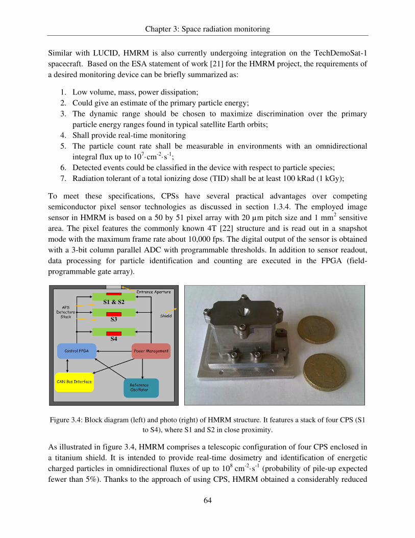
Chapter 3: Space radiation monitoring
64
Similar with LUCID, HMRM is also currently undergoing integration on the TechDemoSat-1
spacecraft. Based on the ESA statement of work [21] for the HMRM project, the requirements of
a desired monitoring device can be briefly summarized as:
1. Low volume, mass, power dissipation;
2. Could give an estimate of the primary particle energy;
3. The dynamic range should be chosen to maximize discrimination over the primary
particle energy ranges found in typical satellite Earth orbits;
4. Shall provide real-time monitoring
5. The particle count rate shall be measurable in environments with an omnidirectional
integral flux up to 107·cm
-2·s
-1;
6. Detected events could be classified in the device with respect to particle species;
7. Radiation tolerant of a total ionizing dose (TID) shall be at least 100 kRad (1 kGy);
To meet these specifications, CPSs have several practical advantages over competing
semiconductor pixel sensor technologies as discussed in section 1.3.4. The employed image
sensor in HMRM is based on a 50 by 51 pixel array with 20 µm pitch size and 1 mm2 sensitive
area. The pixel features the commonly known 4T [22] structure and is read out in a snapshot
mode with the maximum frame rate about 10,000 fps. The digital output of the sensor is obtained
with a 3-bit column parallel ADC with programmable thresholds. In addition to sensor readout,
data processing for particle identification and counting are executed in the FPGA (field-
programmable gate array).
S1 & S2
S3
S4
Figure 3.4: Block diagram (left) and photo (right) of HMRM structure. It features a stack of four CPS (S1
to S4), where S1 and S2 in close proximity.
As illustrated in figure 3.4, HMRM comprises a telescopic configuration of four CPS enclosed in
a titanium shield. It is intended to provide real-time dosimetry and identification of energetic
charged particles in omnidirectional fluxes of up to 108
cm-2
·s-1
(probability of pile-up expected
fewer than 5%). Thanks to the approach of using CPS, HMRM obtained a considerably reduced

Chapter 3: Space radiation monitoring
65
size (15 cm3), mass (52 g). Its particle identification principle based on the particles’ different
penetration capability; the events triggered in different sensor indicate electrons and protons with
different energies.
For the identification of particles species and energies mainly, the HMRM relies on the
innovative architecture: a telescopic configuration of four CPS standard imagers enclosed in a
titanium shield. This study departs from this strategy, indeed it mainly focuses on further
exploring the full potential of a single CMOS monolithic pixel sensor. In order to propose
appropriate specifications for sensor design and estimate the performances of the proposed
sensor, carefully calculations and simulations have been done. Detail introductions and
discussions are described in the following sections.
3.3 From measurement requirements to design specifications: simulation methods and
results
The device simulation is performed to analyse the possibility of CPS to meet the requirements
and provide all the specifications for the following sensor design. According to current NASA
models described in section 3.1, the Earth’s radiation belt consists mostly of protons from about 100 keV up to 400 MeV and electrons from about 10 keV up to 7 MeV. Also the peak
omnidirectional flux of these particles is expected to reach up to several 107/cm
2/s. Due to the
intensities of other cosmic ray ions are several orders of magnitude lower than those of trapped
electron or proton, their effect were ignored in this simulation.
3.3.1 The choice of sensor sensitive area, pixel pitch size and readout speed
Figure 3.5: relations between speed, accuracy, power, sensitive area and pitch size.
The choice of sensor sensitive area, pitch size and readout speed is always a trade-off between
accuracy and power dissipation, as illustrated in Fig. 3.5. For instance, required flux estimate
accuracy may be obtained by employing a certain sensitive area, pitch size, readout speed with
certain power dissipation; a smaller pitch size may lead a higher accuracy while requires a faster
readout speed and sacrifices more power dissipation.

Chapter 3: Space radiation monitoring
66
The accuracy is here defined as the uncertainty of flux estimation. It depends on the target flux
rate, the sampling area and duration; also the detector’s ability to separate close invents on spatial
or time scale.
The expected relative uncertainty of flux estimation is given by:
� = √ = √ = √� (3.1)
Where � is the uncertainty of the measured flux , S is the sensitive area, T is the operation time, α is real flux and N is the number of measured particles. From equation 3.1, we obtain: × = � � (3.2)
Assuming a 10 mm2 sensitive area read out every 20 µs (corresponding to a frame rate of 50
kfps), the lowest particle flux measurable by counting all impinging particles during one second
and with a 10% statistical uncertainty is 103·cm
-2·s
-1. Higher fluxes are estimated either with a
better accuracy or within a shorter time. The highest flux measureable depends on the particle
pileup probability which is governed by the pixel size and the readout rate.
Table 3.1: probability of hits pile-up with respect to sensor operation speed and cluster size.
Frame time
(speed)
Pixel Pitch Clusterize in pixels P (N≥2)
100 µs 20 µm 3×3 0.07%
5×5 0.47%
50 µm 3×3 2.18%
5×5 13.02%
50 µs 50 µm 3×3 0.59%
5×5 3.98%
20 µs 50 µm 3×3 0.10%
5×5 0.72%
The probability of finding exactly n events within time t when the events occur randomly, but at
an average rate of (events per unit time) is described by the Poisson distribution | = � −�! (3.3)
Considering the worst situation, environment average flux as high as 107 particles·cm
-2·s
-1, each
hit triggers a 5×5 cluster. The probability of misjudgment by pile-up two hits in a frame is given
in table 3.1.

Chapter 3: Space radiation monitoring
67
Due to the concern of marginal particle pile-up probability, either of the two options: 20 µm pixel
pitch size with 100 µs frame time or 50 µm pixel pitch size with 20 µs frame time is suitable.
However, smaller pitch size also means more pixels, more processing circuits so as higher power
consumption for a certain sensitive area. As a result, a sensor with 10 mm2 sensitive area, 50 µm
pitch size was chosen. The proposed sensor includes a 64×64 pixel matrix, and its operation
speed is expected to be less than 20 µs per frame.
3.3.2 Simulation of pixel response
In order to obtain more specifics for sensor design, and predict the measurement performances of
the sensor. The complete response of proposed CPS has been simulated with the four following
steps:
1) Generate the various incident particles’ energy deposited in the thin (14 µm) sensitive
area;
2) Calculate the signals over each pixel;
3) Digitize the signals collected on pixels;
4) Program a clustering and hit counting algorithm to group adjacent pixels in a cluster and
sums their digital values to estimate the deposited energy associated from which the
incident particle could be identified.
More details of each step are described in this section.
3.3.2.1 Deposited energy generation
As been described in chapter 1, energy deposited is straggling for particle beams passing through
matter, because of energy loss variance and angular scattering. Mean stopping powers are
therefore not suitable for greater accuracy in realistic situations. However, the data obtained from
the mean stopping powers could provide a general ideal about how particle deposit energy with
respect to their energies and species. Primary decisions, for instance the most angular of sensor
could face to incident particles or appropriate number of ADC bits required to distinguish particle
species, was made based on these simple data. More precise sensor estimated performance was
complemented by Monte Carlo simulations.
Without concerning the energy loss fluctuation, figure 3.6 describes the average energy loss of
electron and proton used to generate e-/h pairs in silicon per µm. In fact, in the energy range
concerned (e- from 100 keV to 7 MeV, proton from 100 keV to 400 MeV), comparing to the
collision energy loss which is used to generate e-/h pairs, other kinds of energy loss are several
magnitude lower which is omitted in this analysis [23]. It tells that protons loss more energy per
µm than electrons and with proton kinetic energy increases its energy loss decreases. This makes
it possible that separates electron/proton particles and tells the energy of incident proton by
measuring their energy deposited in the sensor.

Chapter 3: Space radiation monitoring
68
Figure 3.6: Incident proton and electron energy versus their energy loss used to generate e-/h pairs per µm
in silicon, the vertical dashed lines indicate energy intervals concerned.
Figure 3.6 also illustrates the low energy particles may not penetrate the 14 µm layer, for
instance, 500 keV electron losses 377 keV energy just in 1 µm and it surely losses all of its
energy and stops in the second µm. So the relationship between deposited energy measured and
incident particle kinetic energy is not exactly the same as showed in Figure 3.6.
Considering the simplest situation, particles vertically incident into the sensor, their energy loss
could be measured is the energy lost in the 14 µm epitaxy layer. The total energy loss of proton in
14 µm silicon with respect to its kinetic energy is illustrated in Figure 3.7; from which we could
tell: firstly, protons with energy lower than 700 keV will loss all of their energy and stopped in 14
µm thick silicon; secondly, the energy loss of low energy proton (<700 keV) is comparable with
higher energy proton ((700 keV, 10 MeV)); finally, the measurable energy loss for proton from
700 keV to hundreds of MeV keep decreasing with its kinetic energy increasing.

Chapter 3: Space radiation monitoring
69
Figure 3.7: total energy loss of proton in 14 µm thick silicon with respect to its kinetic energy.
Some very primary conclusions we could make are:
1) In the particle energy range concerned in space radiation, it is possible to identify particle
species (electron or proton) by measuring their deposited energy in CPS epitaxy layer.
Generally, protons deposited higher energy than electrons.
2) Protons’ kinetic energy (from around 1 MeV to hundreds of MeV) is possibly to be
reconstructed due to their monotonically relation with energy deposited.
3) It is not possible to tell incident electrons’ kinetic energy just depends on their deposited energy measured in a single CPS. However, the electron’s penetration capability increases with an increasing kinetic energy. Thereby, a possible method to identify electron’s energy would be using this feature, adding various thick shielding or pile up several
sensors as a telescope. A thin sensor is very desirable with this method, for the easily
multiple scattering feature of electrons.
4) Particles need passing through several µm thick oxide or metal layers (depends on the
layout design and hit position) before they reach the epitaxy layer of CPS. Due to the
limited penetration capability of both low energy particles, the CPS detectable particle
energy may start from several hundreds keV for both electrons and protons.
As described in section 3.1, electrons and protons in space radiation belt have three characteristic
motions, so their incident angular to the detector may vary a lot. As the incident angular could
significantly influence the particle route range in CPS epitaxy layer, which will not only bring
large fluctuation of deposited energy but also various shape and size clusters. Also, different hit

Chapter 3: Space radiation monitoring
70
position affects to the e-/h pairs sharing among neighboring pixels, and then effects to the
measured results. These two effects further complicate the particle identification using a single
sensor. The second step simulation was then performed with the consideration of both the
incident angular and hit position effects.
3.3.2.2 Signal over pixels calculation
The signals generated over each pixel were calculated with a dedicated Monte-Carlo algorithm:
which was developed from many test results of the MIMOSA CPS series with the same sensing
diode size [24]. This algorithm is described by a double Gaussian Point Spread Function (PSF): [� � − +� + −� � − +� ] × � (3.4)
Where x and y is the distance between collecting diode and generated e-/h pairs in x and y
direction; p is the proportion of the double Gaussian; σ and σ is the standard deviation of the
Gaussian function; � is the modified coefficient which depends on the pitch size.
Epitaxial LayerSensing diodes
Incident particle
Figure 3.8: Schematic diagram of particle range in the cross section of epitaxial layer.
As illustrated in Figure 3.8, the particle route range in epitaxial layer is averagely divided into 14
sections (R1 to R14). So the total charge collected on a diode could be calculated as: = ∑ . ×= (3.5)
Where Ctotal represents the total charge collected on a diode, Ei represents the energy deposited in
range section Ri.

Chapter 3: Space radiation monitoring
71
Figure 3.9: Simulation result of signal over pixels for a typical situation: particles hit in junction region of
four adjacent pixels at normal incidence.
Suppose the sensing diode is located in the center of each pixel, the calculation was performed by
MATLAB with electrons and protons of various energies, incident angles and hit positions.
Figure 3.9 shows the result for a typical situation that particles vertically hit the sensor in the
junction of 4 adjacent pixels. The matrix in this figure imitates a cluster with 6×6 pixels; each
square represents a single pixel; the number in each pixel indicates the percentage of total e-
generated in the epitaxial layer and finally collected by each pixel. Results with more details
could be found in table 3.2. Even though they are very primary calculation results which are only
the mean values without considering any energy deposit fluctuation and multiple scattering; some
important conclusions already could be drawn.
This probably is the situation that seed pixel (the pixel collected most of the charges in a cluster)
with the minimum signals. The useful S/N ratio which determines the collection efficiency
should be defined by the minimum seed pixel signals here divided by the noise. As illustrated in
table 3.2, in the energy range concerned, high energy electrons (> 500 keV) have the seed pixel
with minimum signal value which is around 220 e-. In fact, a higher value is expected due to the
electron multiple scattering, this is confirmed by Monte-Carlo simulation in Gent 4 which will be
discussed in section 3.3.3. To simplify the analysis and avoid miss-counting particles, hypothesis
200 e- was the threshold value for a useful counted signal, electrons and high energy protons
would fire a 2×2 cluster while low energy protons (from 500 keV to several MeV) could trigger a
6×6 cluster.
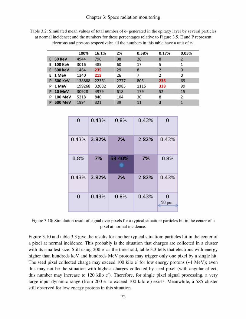
Chapter 3: Space radiation monitoring
72
Table 3.2: Simulated mean values of total number of e- generated in the epitaxy layer by several particles
at normal incidence; and the numbers for these percentages relative to Figure 3.5. E and P represent
electrons and protons respectively; all the numbers in this table have a unit of e-.
100% 16.1% 2% 0.58% 0.17% 0.05%
E 50 KeV 4944 796 98 28 8 2
E 100 KeV 3016 485 60 17 5 1
E 500 keV 1464 235 29 8 2 0
E 1 MeV 1340 215 26 7 2 0
P 500 KeV 138888 22361 2777 805 236 69
P 1 MeV 199268 32082 3985 1115 338 99
P 10 MeV 30928 4979 618 179 52 15
P 100 MeV 5218 840 104 30 8 2
P 500 MeV 1994 321 39 11 3 1
Figure 3.10: Simulation result of signal over pixels for a typical situation: particles hit in the center of a
pixel at normal incidence.
Figure 3.10 and table 3.3 give the results for another typical situation: particles hit in the center of
a pixel at normal incidence. This probably is the situation that charges are collected in a cluster
with its smallest size. Still using 200 e- as the threshold, table 3.3 tells that electrons with energy
higher than hundreds keV and hundreds MeV protons may trigger only one pixel by a single hit.
The seed pixel collected charge may exceed 100 kilo e- for low energy protons (~1 MeV); even
this may not be the situation with highest charges collected by seed pixel (with angular effect,
this number may increase to 120 kilo e-). Therefore, for single pixel signal processing, a very
large input dynamic range (from 200 e- to exceed 100 kilo e
-) exists. Meanwhile, a 5×5 cluster
still observed for low energy protons in this situation.

Chapter 3: Space radiation monitoring
73
Table 3.3: Simulated mean values of total number of e- generated in the epitaxy layer by several particles
at normal incidence; and the numbers for these percentages relative to Figure 3.6. E and P represent
electrons and protons respectively; all the numbers in this table have a unit of e-.
100% 51.8% 7% 2.84% 0.8% 0.43%
E 50 KeV 4944 2561 346 140 39 21
E 100 KeV 3016 1562 211 85 24 13
E 500 keV 1464 758 102 41 11 6
E 1 MeV 1340 694 93 38 10 5
P 500 KeV 138888 71944 9722 3944 1111 597
P 1 MeV 199268 103221 13948 5659 1596 856
P 10 MeV 30928 16020 2165 878 247 133
P 100 MeV 5218 2703 365 148 41 22
P 500 MeV 1994 1033 139 56 16 8
Thus, it seems a low energy proton hit event always means a large cluster size with high seed
pixel charges, with its energy increasing; both the triggered cluster size and seed pixel charges
decreasing; until proton energy increases to several hundred MeV, its trigged event performs
similar with event triggered by a electron. The basic idea of particle identification is based on
their different deposited energy which translates to different triggered cluster size and total
charges collected by fired pixels. Figure 3.11 evaluates these two characteristics in a single plot
for the particles concerned with three incident situations: two normal incident situations we
discussed in figure 3.9 and 3.10, another angular incident situation that particles hit in the center
of a pixel with 80° to Z-direction (θ=80° illustrated in figure 3.8). Obviously, from figure 3.11,
both the trigged pixels number and total e- collected shift a lot for most particles, thus it is almost
impossible to identify a particle’s species and energy with these information. The main reason for
this significant shift is the angular effect, for a particle with the ability to penetrate the sensor, the
length of its route at θ=80° angular incident is cos °⁄ = 5.76 times as long as the route at
normal incident. A proton may even deposit more than 5.76 times energy than normal incident,
because its stopping power increases with its energy decreasing. Therefore, in order to make the
identification possible, it is quite important to limit the incident angles of the particles. This study
has not extended to the aperture design for the detection system; currently, we hypothesis the
finally detection system would have a shielding structure with an aperture to limit the particles’ incident angles as other space radiation detectors introduced in section 3.2. The route length
would be only 1.41 times with θ=45° and 1.15 times with θ=30° as long as normal incident;
thus we ignore the angular effect and just use the data of normal incident to simplify the
following analysis.

Chapter 3: Space radiation monitoring
74
Figure 3.11: sensor responses for various particles with respect to number of pixels fired (threshold 200 e-)
and totally number of e- collected from fired pixels. For each kind of particle, there are 3 points represent
3 incident situations on behalf of hit position or angular effects. Two of them are normal incident with
different position relative to the sensing diode, another is θ=80° as illustrated in figure 3.8.
3.3.2.3 Analogue signals digitization
As discussed in chapter 2, signal digitization is quite meaningful for data processing and
transmission. It would be realized by an ADC in hardware. The first concern for ADC
specification would be a fine resolution to provide useful information. The second concern is a
most possible simplified design with low bit number for low power, high speed operation and
less circuit complexity when the first concern is satisfied.
Results with a discriminator
The simplest ADC, a discriminator is firstly considered. With a discriminator, the particles would
only be identified according to the number of pixels it fired. Figure 3.12 presents the expected
results. For each particle sample, two point “hit in center” and “hit in corner” represent two typical situations: the particle normal incident in the center of a pixel and in the junction region of
four adjacent pixels respectively. Thus, in figure 3.12, the results for other incident situations
probably located in the region between these two points. Generally, the particles could be
classified in to 3 groups by the number of pixels fired in a single hit: low energy protons (<10
MeV), moderate energy protons (from 10 MeV to 100 MeV), high energy protons (> 100 MeV)
and electrons. This energy resolution is achieved just by the intrinsic granularity feature of pixel
sensor; therefore a higher energy resolution can be expected by employing an ADC with more
bits.
100
1000
10000
100000
1000000
0 5 10 15 20 25 30
sum
of
e-
fro
m p
ixe
ls >
th
resh
old
Number of pixels with signal > threshold (200e-)
E 50K
E 100K
E 500k
E 1M
P 100M
P 500M
P 500K
P 1M
P 10M

Chapter 3: Space radiation monitoring
75
Figure 3.12: Total e- generated by various particles with respect to the number of pixels with collected
charges higher than 200 e-.
Results with a 3-bit ADC
To pursue higher particle resolution, an ADC with more bits is mandatory. From table 3.2 and
3.3, we could find electrons and high energy proton just generate several thousand electrons in
total while this number increases one order of magnitude when the proton energy decreases to 10
MeV, and increases another order of magnitude when the proton energy decreases to 1 MeV. For
the final target of particles identification, it seems we do not need an ADC with high energy
resolution in the high deposited energy region, because the number of pixels fired already could
help. In contrast, an ADC with fine resolution in the low and medium deposited energy region
may help in identifying the moderate energy protons and electrons better. After the discriminator,
a 3-bit ADC with 200 e- input threshold was chosen for the analysis. For the idea of separating
electrons with high energy protons, a 700 e- LSB (least significant bit) was chosen, thus electron
fired pixel outputs would always be 1 while high energy proton fired pixel may output 2 at some
occasions (based on the data in table 3.2 and 3.3). Therefore, the ADC would saturate at 4400 e-.
The number of fired pixels and total collected charges could be together expressed as the sum of
ADC counts for all the pixels in a cluster. Thus, particles could be identified by their fired cluster
ADC counts; figure 3.13 shows the simulated result. Compare to the result obtained with a
discriminator, a better resolution for protons is obtained, while electrons and protons with
hundreds of MeV are still mixed together due to their comparable deposited energies.

Chapter 3: Space radiation monitoring
76
(a)
(b)
Figure 3.13: Total e- generated by various particles with respect to sum of 3-bit ADC counts for all the
pixels in a cluster (a) and its sub-region (b).
Results with a 4-bit ADC
In figure 3.13, the cluster ADC counts performance reflect the same trends with the deposited
energy with respect to incident particles’ energy and species as shown in figure 3.7 and discussed in section 3.3.2.1. A smaller LSB wouldn’t help for electrons and high energy (hundreds MeV)
protons separation due to their intrinsic similar deposited energies in the thin epitaxy layer of
0
20
40
60
80
100
120
0 50000 100000 150000 200000 250000
Clu
ster
AD
C c
ou
nts
(3
-bit
)
e- generated
hit in center
hit in corner
0
5
10
15
20
25
30
35
40
0 5000 10000 15000 20000 25000 30000 35000
Clu
ster
AD
C c
ou
nts
(3
-bit
)
e- generated
hit in center
hit in corner
P 500 keV 700keV
E > 500 keV
Sub-region

Chapter 3: Space radiation monitoring
77
CMOS sensor while a larger dynamic range with more bits could help to better separate moderate
energy protons (from 1 MeV to 100 MeV). In order to identify the effect of larger dynamic range,
the same analysis was also performed with a 4-bit ADC which has the same threshold and LSB
with the 3-bit ADC and saturates at 10000 e-. Result is shown in figure 3.14.
(a)
(b)
Figure 3.14: Total e- generated by various particles with respect to sum of 4-bit ADC counts for all the
pixels in a cluster (a) and its sub-region (b).
0
20
40
60
80
100
120
140
160
0 50000 100000 150000 200000 250000
Clu
ster
AD
C c
ou
nts
(4
-bit
)
e- generated
hit in center
hit in corner
0
5
10
15
20
25
30
35
40
45
0 5000 10000 15000 20000 25000 30000 35000
Clu
ster
AD
C c
ou
nts
(4
-bit
)
e- generated
hit in center
hit in corner
E > 500 keV
P 500 keV
700keV
Sub-region

Chapter 3: Space radiation monitoring
78
Compare figure 3.14 with figure 3.13, marginal improvement for particles identification can be
found. As the 3-bit ADC solution already shows a good result, for the second concern mentioned
at the beginning of this section, the 3-bit ADC was finally chosen to digitize the analogue e-
signals collected by the sensor’s sensitive part.
3.3.2.4 Digital signal processing
Based on the analysis in last section, the basic target of the digital signal processing would be
providing the sum of ADC counts for each cluster triggered by individual particles; these
particles could be therefore identified by the different cluster ADC counts information which
reflects their different energy deposited in the sensor.
A clustering and hit counting algorithm was programmed in C++ to emulate the data processing
flow inside the sensor. This algorithm groups adjacent pixels in a cluster and sums their digital
values to estimate the deposited energy associated. An example is shown in figure 3.15 to
indicate its basic operation principle. In figure 3.15, each square in the 8×8 matrix represent a
pixel; the number in each pixel represent the ADC value of its collected signal; and the row on
the bottom means a memory used to temporally store the sum results. There are two clusters in
the matrix means there were two particles hit the matrix in a frame. As introduced in chapter 2,
the sensor operates in rolling-shutter mode, so the data flow from matrix also needs to be
processed row by row. The basic function of cluster identification is realized by trimming non-
zero pixels from zero pixels; the sum results of the adjacent non-zero pixels’ values are temporally stored in the memory at the bottom until there is no non-zero pixels left neighboring;
once the summation of a cluster is finished, the result is readout and memory is reset to 0. In the
example, the two particles triggered two clusters with 20 and 8 ADC counts, based on the last
section analysis, they are probably two protons, one with energy from 30 MeV to 50 MeV,
another with energy around 100 MeV.

Chapter 3: Space radiation monitoring
79

Chapter 3: Space radiation monitoring
80
Figure 3.15 : An example for the basic operation principle of the digital processing.

Chapter 3: Space radiation monitoring
81
3.3.3 Complementary Monte-Carlo simulation and estimated performances
All the previous simulations were based on the particles’ deposited energies calculated from the topping power of particles in silicon; the particles’ routes in silicon were supposed to be straight. Therefore, they are just mean values without considering energy loss fluctuation, electrons
multiple scattering and incident angular effects. In order to better estimate the performances of
the sensor. A complementary Monte-Carlo simulation based on the GEANT4 package had been
done to provide more accurate and reliable deposited energy values. The result is shown in figure
3.16. Particle incident angle θ is considered from 0° to 60°, so particle routes length in silicon
various from Repi to 2Repi, where Repi is the thickness of the epitaxial layer which is typically 14
µm. Electrons deposits more energy than calculated in section 3.3.2.2 due to its routes length in
sensitive area increases by scattering. For electrons, the minimum signal possibly collected by
seed pixel increase to around 300 e- instead of previously calculated 200 e
-. Finally, figure 3.12
indicates the possibility of using a single CPS to distinguish protons from electrons below an
energy of 50 MeV.
Figure 3.16: Monte-Carlo simulation results of energy loss in the sensor’s sensitive area versus particle incident energy.
The 3-bit digital sensor response is also performed based on the Monte-Carlo results and is
shown in figure 3.17. It confirms there is 95% chance electron triggered cluster ADC counts less
than protons below 50 MeV triggered cluster counts; this probability keeps decreasing with
proton energy increasing until 200 MeV proton performs almost the same with electrons.
Meanwhile, protons less than 50 MeV obtain a fine energy resolution by their triggered cluster
ADC counts.

Chapter 3: Space radiation monitoring
82
Electrono Proton
Left: Right:
Figure 3.17: Monte-Carlo simulation results of incident particle energy versus triggered cluster ADC
counts.
Further more, the performances with respect to the dose and particle flux measurements are
displayed in figure 3.18 and 3.19 respectively, and were simulated with the following conditions
1) Each frame (20 µs) contains a number of particles uniformly distributed between 1 and
20.
2) There is a 50/50 mix of electrons and protons with a uniform energy distribution between
1 and 100 MeV.
3) Particles are always normally incident to the pixel surface.
Figure 3.18 shows a linear matching between the reconstructed energy and the deposited one.
The measured standard deviation of the distribution of the difference between the reconstructed
and deposited energy amounts to a relative value of 10%. One observes a deviation of the linear
behavior only for very high ionizing doses (≥ 5 MeV), generated by low energy protons (< 2 MeV).
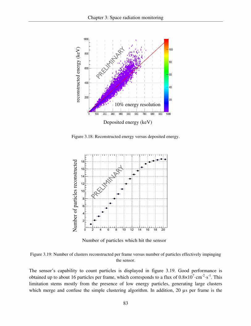
Chapter 3: Space radiation monitoring
83
10% energy resolution
Deposited energy (keV)
reco
nst
ruct
ed e
ner
gy
(keV
)
Figure 3.18: Reconstructed energy versus deposited energy.
Number of particles which hit the sensor
Num
ber
of
par
ticl
es r
econst
ruct
ed
Figure 3.19: Number of clusters reconstructed per frame versus number of particles effectively impinging
the sensor.
The sensor’s capability to count particles is displayed in figure 3.19. Good performance is
obtained up to about 16 particles per frame, which corresponds to a flux of 0.8×10⁷·cm
-2·s
-1. This
limitation stems mostly from the presence of low energy particles, generating large clusters
which merge and confuse the simple clustering algorithm. In addition, 20 µs per frame is the

Chapter 3: Space radiation monitoring
84
limitation of acceptable operation speed discussed in section 3.3.1, any improved operation speed
in sensor design can lead a proportional improvement of this performance. Thus, the current
results should not be taken as an absolute limit of the architecture.
3.4 Conclusions
A CMOS pixel sensor is proposed to be used for the development of miniaturized, accurate and
real-time radiation monitor suitable for widespread use on satellites in Earth orbit. Aiming at
exploit the best particles identification capability with a single CMOS pixel sensor, the proposed
sensor specifications include:
1) A 10 mm2 sensitive area, which contains 64×64 pixels with 50 µm pitch size;
2) Equal or less than 20 µs operation speed for one frame, which means the time needed for
processing one row should ≤ 315 ns in the rolling shutter operation mode; 3) Sensitive input signals from 200 e
- to 4400 e
- for a single sensing diode, and has a relative
linear response in this range.
4) The ability to digitize useful signals into 3 bits; 200 e- threshold and 700 e
- LSB are
required features.
5) A digital processing algorithm embedded right after ADC, which could provide a high
level result by the sensor itself and largely reduce the amount of data at the same time.
Carefully simulations indicate the proposed CPS could reconstruct particles deposited energy
with in 10% relative uncertainty, thus protons with energy less than 50 MeV could be
distinguished from electrons, higher energy protons are probably confused with electrons due to
their intrinsic highly similar amount of energy deposited in the thin epitaxy layer of CPS. The
estimated particle count ability reaches to about a flux of 107·cm
-2·s
-1 which is considered as the
peak omnidirectional fluxes in the Earth orbit radiation environment.

Chapter 3: Space radiation monitoring
85
Bibliography
[1] T. A. Farley and A. D. Tomassian. Source of high-energy protons in the Van Allen radiation
belt. Phys. Rev. Lett., 25:47-49, 1970.
[2] Wikipedia: Van Allen radiation belt.
http://en.wikipedia.org/wiki/File:Van_Allen_radiation_belt.svg#filelinks
[3] D.M.Sawyer and J. I. Vette, AP-8 trapped proton environment for solar maximum and solar
minimum, 1976 NASA TM-X-72605.
[4] J. I. Vette, The AE-8 trapped electron model environment, 1991 NSSDC/WDC-A-R&S 91-24
[5] J. R. Cummings et al. New evidence for geomagnetically trapped anomalous cosmic rays.
Geophys. Res. Lett., 25:47-49, 1970.
[6] J. A. Van Allen et al. Radiation observations with satellite 1958 . J. Geophys. Res., 64: 271-
286, 1959.
[7] J. A. Van Allen. The geomagnetically trapped corpuscular radiation. J. Geophys. Res., 64:
1683-1689, 1959.
[8] M. Cyamukungu et al. Magnetic storm acceleration of radiation belt electrons observed by the
Scintillating Fibre Detector (SFD) onboard EQUATOR-S. In Ann. Geophys., volume 17, pages
1622-1625, 1999.
[9] B. Taylor et al. Results from the Galileo GioveA radiation monitors and comparison with
existing radiation belt models. IEEE Trans. Nuc. Sci., 54:1076-1081, 2007.
[10] S-J. Kim et al. Use of a MOSFET for radiation monitoring in space and comparison with the
NASA trapped particle model. J. Korean Phys. Soc., 48:865-869, 2006.
[11] I. Thomson et al. Dose-depth and SEU monitors for the STRV-1c satellite. IEEE Trans. Nuc.
Sci., 45:2765-2770, 1998.
[12] A. Mohammadzadeh et al. The ESA Standard Radiation Environment Monitor program first
results from PROBA-I and INTEGRAL. IEEE Trans. Nuc. Sci., 50:2272-2277, 2003.
[13] H. D. R. Evans et al. Results from the ESA SREM monitors and comparison with existing
radiation belt models. Adv. Space Res., 42:1527-1537, 2008.
[14] M. Siegl et al. Inner Belt Anisotropy Investigations Based on the Standard Radiation
Environment Monitor (SREM). IEEE Trans. Nuc. Sci., 57:2017-2023, 2010.
[15] T. S. Lomheim et al, Imaging Charge-Coupled Device (CCD) Transient Response to 17 and 50
MeV proton and Heavy-Ion Irradiation, IEEE Transactions on Nuclear Science, Vol. 37, No. 6,
p. 1628-1637, December 1990.

Chapter 3: Space radiation monitoring
86
[16] A. M. Chugg et al. A CCD miniature radiation monitor. IEEE Trans. Nuc. Sci., 49:1327-1332,
2002.
[17] L. S. Pinsky et al. Preparing for the first Medipix detectors in space. In Aerosp. Conf. Proc.,
pages 1-6, 2012.
[18] X. Llopart et al. Timepix, a 65k programmable pixel readout chip for arrival time, energy
and/or photon counting measurements. Nucl. Instrum. Meth. A, 581:485-494, 2007.
[19] L. S. Pinsky et a. Penetrating heavy ion charge and velocity discrimination with a TimePix-
based Si detector (for space radiation applications). Nucl. Instrum. Meth. A, 633:S190-S193,
2011.
[20] N. Guerrini et al. Design and characterization of a highly miniaturized radiation monitor
HMRM. Nucl. Instrum. Meth. A, 731:154-159, 2013.
[21] ESA directorate of technical and quality management. Statement of work: Highly miniaturised
radiation monitoring and highly miniaturised active MEO radiation monitor Ph. A-B. T604-
001EE and T704-027EE, 2009.
[22] R. Coath et al. A low noise pixel architecture for scientific CMOS monolithic active pixel
sensors, IEEE Trans. Nucl. Sci. NS 57, 5, 2010.
[23] Stopping-power and range tables for protons and electrons. NIST (National institute of
standards and Technology) Physical Meas. Laboratory.
http://physics.nist.gov/PhysRefData/Star/Text/PSTAR.html for protons;
http://physics.nist.gov/PhysRefData/Star/Text/ESTAR.html for electrons.
[24] A. Besson, The AIDA-SALAT simulator, September, 6 - 9, 2011 Mont Sainte Odile, France.

87
Chapter 4
General COMETH architecture
According to the previous study and simulations described in chapter 3, a CPS named as
COMETH was proposed. It features a sensitive area of 3.2×3.2 mm2, comprising 64×64 square
pixels with a 50 µm pitch size. A single 4.3×4.3 µm2 n-well/p-epi sensing diode locates at the
center of each pixel. The size and position of the sensing diode was chosen to be the same with
these MIMOSA chips used to generate the PSF (Point Spread Function) which is the foundation
of the simulations introduced in chapter 3. Right after the sensing diodes, the signal processing
chain mainly contains three parts: analogue signal processing, analogue to digital conversion and
digital signal processing. This chapter is going to introduce how the constraints and specifications
for the design of these parts were draw from all the previous study. Each part will be discussed
respectively and the global architecture will be introduced at the end of this chapter.
4.1 The analogue signal processing
Simulation introduced in chapter 3 indicates the useful charge may collected by a single diode
varies from around 300 e- to exceed 100 kilo e
-. The signal could be either very weak or
extremely strong. The voltage drop generated on the charge sensing diode by these small signals
typically being of the order of several mV; while these large signals could easily complete
discharge the sensing diode.
The self-biased pixel architecture used in MIMOSA 26 was demonstrated to have low noise and
good radiation tolerance; however it takes more time to recharge the diode than the reset
architecture. COMETH not only has to face a continuously high particle flux environment but
also would be completely discharged by these large signals. The reset architecture was chosen
instead of self-biased architecture, so the sensing diode could recover quickly from large signals
and get ready for the next coming event.
Similar with MIMOSA 26, the smallest useful signal and the Fixed Pattern Noise (FPN) are
about the same order of magnitude, and due to the need for further on-chip data sparsification.
The main concern for the signal processing right after the sensing diode would be signal
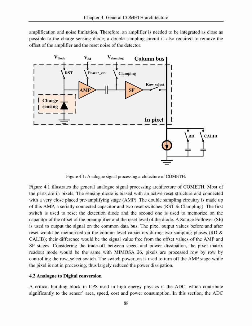
Chapter 4: General COMETH architecture
88
amplification and noise limitation. Therefore, an amplifier is needed to be integrated as close as
possible to the charge sensing diode; a double sampling circuit is also required to remove the
offset of the amplifier and the reset noise of the detector.
Vdiode Vdd Vclamping Column bus
AMP SF
Charge
sensing
Row select
ClampingPower_onRST
RD CALIB
In pixel
Figure 4.1: Analogue signal processing architecture of COMETH.
Figure 4.1 illustrates the general analogue signal processing architecture of COMETH. Most of
the parts are in pixels. The sensing diode is biased with an active reset structure and connected
with a very close placed pre-amplifying stage (AMP). The double sampling circuitry is made up
of this AMP, a serially connected capacitor and two reset switches (RST & Clampling). The first
switch is used to reset the detection diode and the second one is used to memorize on the
capacitor of the offset of the preamplifier and the reset level of the diode. A Source Follower (SF)
is used to output the signal on the common data bus. The pixel output values before and after
reset would be memorized on the column level capacitors during two sampling phases (RD &
CALIB); their difference would be the signal value free from the offset values of the AMP and
SF stages. Considering the trade-off between speed and power dissipation, the pixel matrix
readout mode would be the same with MIMOSA 26, pixels are processed row by row by
controlling the row_select switch. The switch power_on is used to turn off the AMP stage while
the pixel is not in processing, thus largely reduced the power dissipation.
4.2 Analogue to Digital conversion
A critical building block in CPS used in high energy physics is the ADC, which contribute
significantly to the sensor’ area, speed, cost and power consumption. In this section, the ADC
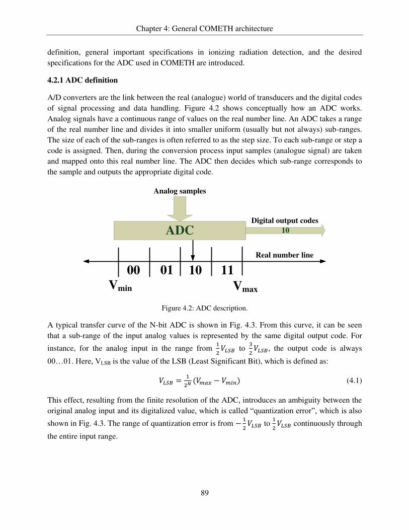
Chapter 4: General COMETH architecture
89
definition, general important specifications in ionizing radiation detection, and the desired
specifications for the ADC used in COMETH are introduced.
4.2.1 ADC definition
A/D converters are the link between the real (analogue) world of transducers and the digital codes
of signal processing and data handling. Figure 4.2 shows conceptually how an ADC works.
Analog signals have a continuous range of values on the real number line. An ADC takes a range
of the real number line and divides it into smaller uniform (usually but not always) sub-ranges.
The size of each of the sub-ranges is often referred to as the step size. To each sub-range or step a
code is assigned. Then, during the conversion process input samples (analogue signal) are taken
and mapped onto this real number line. The ADC then decides which sub-range corresponds to
the sample and outputs the appropriate digital code.
00 01 10 11Vmin Vmax
ADC 10
Digital output codes
Analog samples
Real number line
Figure 4.2: ADC description.
A typical transfer curve of the N-bit ADC is shown in Fig. 4.3. From this curve, it can be seen
that a sub-range of the input analog values is represented by the same digital output code. For
instance, for the analog input in the range from to , the output code is always
00…01. Here, VLSB is the value of the LSB (Least Significant Bit), which is defined as: = − (4.1)
This effect, resulting from the finite resolution of the ADC, introduces an ambiguity between the
original analog input and its digitalized value, which is called “quantization error”, which is also shown in Fig. 4.3. The range of quantization error is from − to continuously through
the entire input range.

Chapter 4: General COMETH architecture
90
Digital Output (N-bit)
11...10
00...11
00...10
00...01
11...01
00...00
VLSB 2VLSB 3VLSB (2N-3)VLSB (2
N-2)VLSB (2
N-1)VLSB
½ VLSB
-½ VLSB
Analog Input
Vin
Qu
an
tiza
tion
erro
r
Figure 4.3: Typical transfer curve of an N-bit ADC.
A comparator is the basic and essential element of an ADC. It is a device that compares two
voltages or currents and makes a decision based on which of the quantities is larger. The
operation of a comparator is illustrated in figure 4.4. It has two analogue input terminals Vi and
VR and one binary digital output Vo. Ideally, Vo equals to 1 or 0 indicating which input is larger.
Vi
VR
Vo
VR
Vo
Vi
Figure 4.4: Comparator Circuit and Transfer Function.

Chapter 4: General COMETH architecture
91
4.2.2 ADC Characterization
The number of output bits from an A/D converter does not fully specify its behavior. Real A/D
converters can differ from ideal behavior in many ways. Ultimately, the application determines
the requirements, and A/D converter resolution may not be either necessary or sufficient to
specify the required performance. Some of the most important characteristics describing the
performances of the ADC are introduced below.
Resolution
Resolution describes the fineness of the quantization performed by the ADC. For a fixed full
scale input range, a high resolution ADC can resolve smaller signals than a low resolution ADC
is able to resolve. It is usually defined as the number of distinct analog levels corresponding to
the different digital words. Therefore, an N-bit resolution implies that the converter can resolve
2N distinct analog levels. Resolution is usually degraded by either noise or nonlinearity.
Offset and Gain error
In an ideal ADC, a specific input signal of Vthreshold will cause the output code passes from zero to
one. Any deviation from this point is called the Offset Error. It is defined to be the input analog
signal that should produce zero output. It can be expressed as the deviation of V00…01 from
Vthreshold, given by the following equation: = … − ℎ ℎ� (4.2)
The unit is LSB. The Offset error is a constant and can be calibrated out.
The Gain Error is defined to be the difference at the full-scale value between the ideal and actual
curves when the Offset Error has been reduced to zero. For an ADC, it is given by: = .. − …� − − (4.3)
Where V00…01 and V11…11 represent respectively the transition voltages for the codes 00…01 and 11…11, which are ½ VLSB and − + in the ideal case.
Graphically, the Offset and Gain Error are illustrated in Fig. 4.5.

Chapter 4: General COMETH architecture
92
11...11
Digital Output (N-bit)
11...10
00...11
00...10
00...01
11...01
00...00
Analog Input
Vin
VLSB 2VLSB 3VLSB (2N-3)VLSB (2
N-2)VLSB (2
N-1)VLSB
Ideal characteristic
Real characteristic
Offset error
(a) Offset error of an N-bit ADC
11...11
Digital Output (N-bit)
11...10
00...11
00...10
00...01
11...01
00...00
Analog Input
Vin
VLSB 2VLSB 3VLSB (2N-3)VLSB (2
N-2)VLSB (2
N-1)VLSB
Ideal characteristic
Real characteristic
Gain error
(b) Gain error of an ADC.
Figure 4.5: Offset and gain error of an N-bit ADC. It is assumed that all other errors are not presented.

Chapter 4: General COMETH architecture
93
Nonlinearity
Some applications, such as telephone codecs, require an ADC that is intentionally nonlinear.
However, most ADCs are intended to have a transfer characteristic that approximates a straight
line. As the resolution increases, the input-output characteristic of the ADC approximates a
straight line; the transfer characteristic for an ideal version of such and ADC progresses from low
to high in a series of uniform steps. Due to this fact, nonlinearity exists even in an ideal ADC.
The transfer characteristic of a practical ADC contains steps which are not perfectly uniform, and
this deviation generally contributes to further nonlinearity. Two types of nonlinearity are used to
characterize this deviation.
11...11
Digital Output (N-bit)
11...10
00...11
00...10
00...01
11...01
00...00
Analog Input
Vin
VLSB 2VLSB 3VLSB (2N-3)VLSB (2
N-2)VLSB (2
N-1)VLSB
Ideal characteristic
Real characteristic
Code Width = 2 LSB
DNL = 1 LSB
INL = 3/4 LSB
Figure 4.6: Example Transfer Characteristic of an N-bit ADC Showing DNL and INL.
A. Integral Nonlinearity (INL) error
The INL of the ADC measures the straightness of the transfer function. It is defined as the
difference between the actual transfer characteristic and the straight line characteristic which the
ADC is intended to approximate. Practically, it can be calculated by the differences between the
real output code and the ideal output code.
B. Differential Nonlinearity (DNL) error

Chapter 4: General COMETH architecture
94
The DNL of the ADC describes the error in each step size. It measures how far each of the step
sizes deviates from the nominal value of the step size. The differential nonlinearity is zero if
every transition to its neighbors equals 1LSB. It is given by: = + − − (4.4)
Qm+1 and Qm are two adjacent quantization levels. Ainput(Qn) is the analog input voltage
corresponding to the quantization level Qn.
DNL and INL are both plotted as a function of code and generally expressed in terms of LSB.
Figure 4.6 illustrates DNL and INL.
AD conversion time and Sampling rate
In an ADC, the conversion time is the time needed for the converter to complete a full single
measurement including sampling of the input signal and output the digital codes. The sampling
rate is the inverse of the conversion time, which indicates the number of times the input signal is
sampled per second.
Signal-to-Noise ratio (SNR)
For an ideal N-bit ADC, the maximum output signal is the full scale signal and the output noise is
due to the quantization noise. As − < < , the error due to the quantization noise is
� = √ � ∫_ �� = �√ (4.5)
While the rms value of a full-scale peak-to-peak amplitude VFS is √⁄ . The SNR of an ideal
N-bit ADC when the noise is due only to quantization can be directly calculated and given by:
= √⁄� = � √⁄� √⁄ = √
(4.6)
Converting into decibel result is:
= . + . (4.7)
Dynamic range
Dynamic range is a measure of the range of input signal amplitudes for which useful output can
be obtained from a system. It can be defined as the ratio between the maximum and the minimum
of input signals that can be resolved by the converter. As the minimum input signal is equal to

Chapter 4: General COMETH architecture
95
VLSB, the dynamic range of an ideal N-bit ADC equals to its maximum SNR which is given by the
equation 4.7.
Power Dissipation
For the ADCs been implemented in large systems without sophisticated cooling (e.g. vertex
detector introduced in chapter 2) or portable systems powered by a battery with limited energy
(e.g. highly miniaturized space radiation monitor), power dissipation is becoming an important
specification. Reducing power dissipation can help in maintaining the system temperature or
improving the battery life.
4.2.3 Specifications for the ADC used in COMETH
The ADC required by COMETH should digitize the analogue signal from pixels into 3-bit and
provide the digital results to the following processing block. Therefore, its operation mode and
conversion time should match with the analogue processing of each pixel; its data output mode
should be easier for further processing; simple and low power consumption architecture are better
while the desired characteristics are satisfied.
The most primary specification for the 3-bit ADC used in COMETH is implementation level
which will almost affect every aspects of the ADC design even the whole processing system.
There are three ways to implement an ADC on CPS:
1. Chip-level, where a single ADC circuit serves the whole APS array. This method does not
suffer from the performances variation from one ADC to another; however it requires a
very high speed convertor for a large frame rate and high pixel count applications.
2. Column-level, where each column has a dedicated ADC, forming a single array of A/D
converter serving the entire APS. All these ADCs operate in parallel, so a low-to-medium
speed ADC design can be used, depending on the array size. The problem of such an
approach is mismatch between the ADC on different columns giving rise to fixed pattern
noise.
3. Pixel-level, where every pixel has its own converter. This allows extremely parallel
operation of all ADCs in the APS array resulting in high speed conversion and faster
readouts. Also it eliminates read related column fixed-pattern noise and reduces the
analog circuit requirement for Correlated Double Sampling (CDS). Using one ADC per
pixel has advantages of higher SNR, low power consumption and simpler design. One
main disadvantage however is fixed-pattern noise due to mismatch variation could be
much worse.
To avoid particle pile-up, the operation speed of COMETH is foreseen to be less than 20 µs per
frame. The required sampling rate for a chip-level ADC implemented should at least be:

Chapter 4: General COMETH architecture
96
. = ×× −6 ≈ / (4.8)
Although it is a quite high speed requirement, it still can be satisfied by a flash or folding and
interpolating ADC [1]. However, the chip-level ADC would process signals and provide results
pixel by pixel; the successive data providing mode would require extra memories for the
following digital processing which is based on the data map of the whole matrix in each frame. In
addition, these high speed ADCs typically suffer from low accuracy, large area and high power
dissipation.
Analysis by several authors [2, 3] shows that pixel level ADC should achieve the highest SNR
and the lowest power consumption, since it is performed in parallel, close to where the signals are
generated, and operates at low speed. However, for CPS used in radiation detection, the use of
PMOS transistors inside the pixel array is restricted in most processes, since PMOS transistors
are placed in n-well which would compete for charge collecting with the sensing N-well diode.
Therefor, in most of processes, pixel-level ADC is unsuitable for radiation detection.
Column level implementation provides a promising solution. Comparing to the chip-level ADC,
the required sampling rate of column ADC for COMETH would reduce 64 times which would be
around 3.2 MS/s. The release of the speed requirement could lead to an improved accuracy, and
simpler design. Row by row provided data is also release the large memory or highly speed
requirement for the following digital processing.
As described in chapter 3, the average hits per frame on COMETH are less than 20. Most of the
hits trigger clusters with less than 4 pixels. Averagely, more than 97% of the 4096 (64×64) pixels
are unfired during the operation. The ADC is better to have a “sleep” mode for the signals lower than a preset “threshold” value through which could efficiently save the power dissipation. In
addition, most of the signal data after 3-bit digitization provided to the digital processing block
would be ‘000’, an extra bit which tells the 3-bit signal value is ‘0’ or not would be a plus for the
following digital algorithm.
Thereby, the desired digitization block for COMETH would be realized by column-level 3-bit
ADC which provides 4-bit data containing an extra bit to tell the signal value is ‘0’ or not. The ADC operation should match with the pixel signal processing. Constrained by the pixel pitch, the
layout of column-level ADC should be implemented in the rectangle area with 50 µm width.
4.3 The embedded digital signal processing
The sensor’s digital response after the 3-bit digitization would be as emulated in figure 4.7. The
foremost concern of the following digital signal processing logic is to get the desired
functionality right. As described in section 3.3.2.4, the basic required functions include:
1. Clusterization: which is recognizing the fired pixels belongs to one cluster (fired by a
single hit);

Chapter 4: General COMETH architecture
97
2. Summation: sum all the pixels’ ADC outputs that belong to the same cluster;
3. Separation: based on the different addition results, which represent the various particle
species and energies, separate the events to different memories;
4. Counting: count the events of different memories and directly output the counting results
from different memories.
Then, in order to realize real-time data providing, its operation rate should match with the ADC
data providing rate.
Figure 4.7: Emulated COMETH 3-bit digitized response of one frame.
4.4 Global architecture of COMETH
Figure 4.8 (a) illustrates the global architecture of the proposed sensor COMETH. A 64×64
pixels matrix operates in the rolling shutter operation mode; 64 column 3-bit ADCs are used to
digitize the analogue signals from pixels row by row; the data flow provided by ADCs are
processed by the embedded digital processing logic in real-time; the final outputs are expected to
directly provide the particles’ flux information by their species and energies. Its required operation speed is at least 50,000 frames per second aiming at a particle count ability about
107·cm
-2·s
-1 with marginal error due to particle pile-up.
The first prototype without the digital processing logic was design and fabricated in a 0.35 µm
process during summer 2012. It features a reduced scale with 32×32 pixels and 32 column ADCs;
its layout is shown in figure 4.8 (b). The embedded identifying and counting algorithm was also
designed and simulated in the same process. The design and test details of each signal processing
part will be introduced in the following chapters.

Chapter 4: General COMETH architecture
98
Pixel Pixel Pixel Pixel
Pixel Pixel Pixel Pixel
Pixel Pixel Pixel Pixel
Pixel Pixel Pixel Pixel
Per Column 3-bit ADC
Row
sel
ecti
onL
ogic
Blo
ck
Col
un
m o
utp
ut
lin
e
Output
Intelligent processing
Memory
(a) (b)
Figure 4.8: Global architecture of COMETH (a) and the layout (3.5 mm × 4 mm) of the first reduced scale
prototype (b).

Chapter 4: General COMETH architecture
99
Bibliography
[1] Imran Ahmed. Pipelined ADC Design and Enhancement Techniques. Analog Circuits And
Signal Processing, Springer, 2010.
[2] U. Ringh, et al. Readout concept employing a novel on Chip 16 bit ADC for smart IR focal
plane arrays. Proceedings of SPIE, Vol. 2745, 1996.
[3] B. Pain, et al. Approaches and analysis for on-focal-plane analog-to-digital conversion.
Proceedings of SPIE, Vol. 2226, 1994.

100
Chapter 5
Analogue signal processing
In COMETH, the key design points of the analogue signal processing right after the sensing
diode are a high SNR for the smallest expected signals (300 e-) and a relative linear response for
the concerned signal range (up to 4400 e-); meanwhile, a processing time less than 312 ns per
pixel (corresponding to 20 µs per frame), the diode fast reset and complete recovery from large
signals and low power dissipation are also required. This chapter is going to describe the design
details and the test results obtained with X-rays, ß- particles and laser illumination which confirm
the sensitivity and simulated responses of this sensor technology to electrons.
5.1 Pixel design
The analogue signal processing mainly concentrated in the pixel. As discussed in section 4.1, the
final chosen pixel schematic and its operation timing are illustrated in figure 5.1.
Vset
Vdd
PWR_ON
RST1 RST2
Row_select
SF_bias
RD
CALIB
CS
SF
E
Pixel
Column
Vclp
CPP
(a)

Chapter 5: Analogue signal processing
101
240 ns
Poweron
Row_selct
Read
Reset1
Reset2
Calib
Fck = 100 MHz
480 ns
(b)
Figure 5.1 : (a) Schematic of the pixel and, (b) related timing.
The schematic consist a sensing diode with active reset structure, a double sampling circuit, and a
Source Follower (SF). The active reset structure helps the diode recover quickly from high flux
and large signal environment; the double sampling is used to suppress reset noise of the diode
capacitance and pixel-to-pixel offset non-uniformities; and the source follower is used to output
the signal on the column data bus.
The in-pixel double sampling circuit is employed due to the limited achievable CVF (~20 µV/e-
maximum) with the sensing diode and the small signals (several hundreds of electrons) concerned
in COMETH application; an amplify stage and double sampling are employed to obtain a higher
CVF and overcome the residual pixel-to-pixel and column-to-column fixed pattern noise. The
double sampling circuit is made up of a Common Source (CS) preamplifier, a serially connected
poly to poly capacitor (CPP in figure 5.1) and two reset switches. One switch (RST1) is used to
reset the detection diode and the other one (RST2) is used to memorize the offset of the pre-
amplifier on the capacitor as well as the reset level of the diode. “Read” and “CALIB” are column level commands to memorize the output signal level and the column reference level
respectively. The operation is as follows.
During offset sampling phase, both switches RST1 and RST2 are closed, so that the offset
of CS is memorized on the series capacitor CPP. The value is AVoff_CS, where A is the
gain of the CS stage.
After that, the RST1 open firstly. Because RST2 remains closed at this moment, the reset
noise of the RST1, intensified by the gain of CS, is also memorized on CPP. Then RST2
opens, the value memorized on the capacitor CPP is equal to: A(Voff_CS + Vnoise_rst1).

Chapter 5: Analogue signal processing
102
After integration, when the signal is readout, the offset of CS and the reset noise of RST1
could be compensated thanks to the information stored on CPP. The following operation
is performed:
A(Vsig + Voff_CS + Vnoise_rst1) – A(Voff_CS + Vnoise_rst1) (5.1)
The remaining value after readout is then equal to AVsig, free of the offset of CS stage and
the reset noise of RST1.
During the Read phase (readout of the signal), the voltage VRD, sampled by the readout
circuitry, is the signal value which contains the offset of the SF stage.
During the Calib phase (readout of the reference level), the pixel readout and sampling the
reference level VCALIB, it also contains the offset of the SF stage.
Finally, the useful signal is the difference between these two levels, free from the offset
mismatches of the SF stage. The noise sources not being removed after the above process are the
reset noise of RST2 and the 1/f noise. However, the reset noise voltage of RST2 is equal
to√ ⁄ , it could be reduced by selecting a large value of CPP and the 1/f noise is very small
because the pixel is designed for high speed operation.
The key points of this design are:
Only NMOS transistors are used in this architecture, since any PMOS transistors would
compete for charge collection with the sensing N-well diode.
The reset transistors (RST1, RST2) should remain in linear region for a fast reset. It
requires, for the two reset transistors RST1 and RST2, − > ℎ. Since the logic
level applied on their gate as the command is 3.3 V and ℎ is about 0.7 V, the reference
voltages chosen for RST1 and RST2 should be less than 2.6 V.
The CS stage should remain in appropriate operation region. It requires trade off among: a
higher gain for a larger CVF, an efficient input dynamic range and a relative linear
response.
The selecting value of CPP is better to be large to reduce the reset noise of RST2;
however, a large CPP value requires a long time for its previous CS stage obtaining a
stable output which will limit the whole pixel operation speed. In this design, for the noise
concern, a large value of CPP (150 fF) is chosen, thus the operation speed is slightly
sacrificed.
There are two occasions the CS stage output required to be stable during the operation,
one is before the signal reading (read) and the other is before calibration (calib). To
provide enough time for the CS stage output getting stable before signal reading, the CS

Chapter 5: Analogue signal processing
103
stage should be powered on (poweron) before the pixel is selected to read (row_select). In
fact, to simplify the sequence, during the operation two rows are powered on (power_on)
while only one row is selected to read (row_select), thus 270 ns is left for the CS stage
output getting stable before signal reading which is more than enough. For the second
occasion, the right side voltage of the CPP should keep at Vclp (Reset2) until its left side
voltage getting stable; insufficient reset2 timing would leave a residual small signal for
the very next frame while a large signal occurs. It requires 100 ns (Reset2) for this design.
The SF stage should remain in appropriate operation region. Its input dynamic range
should match with the output range of the previous CS stage; it should have a stable gain
and supply efficient current to drive the following column processing.
5.1.1 The CS pre-amplify stage
As represented in Fig. 5.2, the simplicity of the CS amplifier reduces the offset mismatches of the
transistors, while the design of it is crucial to the pixel performance. A high gain is desirable to
achieve a high CVF, but it generally requires a high output resistance, increased input
capacitance, reducing the input dynamic range, degrading the speed, linearity and the noise
performance of the circuit.
Vdd
PWR_ON
Vin
Vout
M1
M2
M3
Figure 5.2: Common source amplifier stage used inside the pixel.
The transistors M1 and M3 make up the amplifier, where M1 is the load of M3. The voltage gain
of the amplifier is given by:
= −√ ⁄⁄ +� (5.2)
where W and L are respectively the width and the length of the transistor channel. In the
equation, � is equal to . Here, is the transconductance of M1 and is defined as � ��

Chapter 5: Analogue signal processing
104
of M1 where ID is the current passing through the drain of M1 and VBS is the bulk to source
voltage of M1.
One additional transistor (M2) is added in the basic architecture. It is used as a switch to cut off
the power of the CS stage when the pixel is in the integration mode. For this transistor, a rather
high W/L (length to width ratio of the transistor channel) is preferable in order to reduce the turn
on resistance, so that it has only very slight effect on the performance of the CS stage.
M3 transfers the input voltage into current. In order to obtain a high voltage gain and a fast
conversion, the minimum L should be used and a large value of W is preferred. However, the
charge detection diode is connected with M3, so increasing the value of W of M3 means to
increase also the parasitic capacitance around it, decreasing the corresponding CVF value.
Therefore, moderate value of W is chosen to ensure a reasonable current and the voltage gain is
mainly obtained by varying W/L of M1. Several different values of W/L are tested in the
simulation. Fig. 5.3 shows the simulation results of static characteristics of the CS stage.
2µ/1µ 1µ/1µ 0.5µ/1µ 0.35µ/12µ0.55µ/12µ1µ/5µ 1µ/10µ
(a) Input-output voltage characteristic
(b) Voltage-current characteristic of M3

Chapter 5: Analogue signal processing
105
│Gain
│
(c) Absolute values of the voltage gain
Figure 5.3: Static characteristics of the CS stage under different W/L values of M1.
It can be seen that with the W/L ratio of M1 decreases, the absolute value of the voltage gain
increases and the corresponding dynamic range decreases. In this design, the compromise is
reached with a W/L ratio of 0.55µ/12µ. As illustrated in Fig. 5.4, the absolute gain value is from
3.8 to 4.2 with a dynamic range of 250 mV which corresponding to collected signal charge
around 10000 e-.
│G
ain│
Vout│Gain│
250 mv
Figure 5.4: Static characteristics of the CS stage with W/L ratio of M1 equals to 0.55µm/12µm.

Chapter 5: Analogue signal processing
106
This 10000 e- signal range used in design is almost twice the signal value concerned (0 to 4400 e
-
) and used for energy reconstruction introduced in section 3.3.2.3. It is because the gain of the CS
amplifier is not stable and linear all over its operation region; the realistic variations in the
process and fluctuation of bias voltages to each pixel in the matrix may drive some pixels out of
its appropriate operation region. To keep the identity of pixels performances for a matrix
containing thousands of pixels as much as possible, a margin room was left in this design.
Since the collected charge and the stage changing of RST1 both lower the input voltage of the CS
stage, the Vset level is chosen as 950 mV in this design. From Fig. 5.3 (b), it can be seen that the
current passing through the transistor is only about 6 µA if 800 mV is chosen to be the common
mode level on the input. As a result, the consumption of the CS stage is about 20 µW when it is
powered on.
5.1.2 The SF stage
Fig. 5.5 shows the static characteristic of the SF stage which is realized by N-MOS transistor.
From Fig. 5.4, the useful output dynamic range of the CS stage is about 1 V. Thus, the SF input
reference level (Vr2) is set to 1.6 V to obtain a relative stable gain about 0.83 in the 1 V input
range. Its current bias is set to 35 µA to drive the following column circuits.
1 V
VoutGain
Figure 5.5: Gain and input-output voltage characteristic of the SF stage.

Chapter 5: Analogue signal processing
107
5.1.3 The global pixel performance
Taking into account the CS stage and the SF stage together, the pixel’s global gain is about 3.3 and the phase shift is 180° introduced by the CS stage. Using the timing diagram shown in Fig.
5.1 (b), the corresponding readout time of one frame is: = × × = × × = . µ (5.3)
This is less than the previous introduced 20 µs per frame time limitation. In this architecture, after
RST1 and RST2, the reset level is memorized on the coupling capacitor. The reset noise due to
RST1 is also memorized because RST2 is still ‘on’ when RST1 is turned off. Moreover, offset mismatches of the amplifiers are memorized too. During the next readout of the pixel, all these
noise are automatically eliminated by subtracting from the signal. In order to simulate the offset
cancellation operation, an offset of the range from -50 mV to 50 mV is added on the input of the
CS stage. The results are shown in Fig. 5.6.
Com
man
d
sign
als
(V
)P
ixel
in
pu
t
(mV
)
CS
sta
ge
ou
tpu
t (V
)
Pix
el o
utp
ut
(mV
)
Time (µs)
Offset = 0mVOffset = 50mV Offset = -50mV
Read Calib
Reset1
Reset2
204 mV
197 mV
3.6 mV
1.6 mV
Figure 5.6: Simulation of the in-pixel offset cancellation operation.
It can be seen that the outputs of the CS stage for -50 mV and 50 mV offset are 204 mV and 197
mV, respectively. At the end of RST2, these two values are mostly memorized on the series
capacitor. The final residual error on the output of the pixel are only 3.6 mV for -50 mV offset
input and 1.6 mV for 50 mV offset input. Considering the gain of the system (about 3.3), these

Chapter 5: Analogue signal processing
108
values mean that the input equivalent offset is only about 1 mV in this condition. Thus, it proves
this pixel architecture is quite efficient for offset cancellation.
The power dissipation for a single pixel is estimated to be 135 µW. For the whole pixel matrix
operation in rolling shutter mode, the total power dissipation is estimated to be 8.64 mW (135
µW × 64).
5.2 Test of the pixel matrix
A reduced scale prototype with 32×32 pixels and 32 column ADCs was fabricated in a 0.35 µm
process, and tested to validate the COMETH concept. Dedicated analogue outputs for the
centered 8 columns, bypassing the ADC, were foreseen in order to characterize in detail the pixel
response.
The pixel matrix was illuminated with three types of radiations: monochromatic X-rays to obtain
the charge to voltage conversion factor (CVF) and the charge collection efficiency (CCE); Beta
electrons to assess the sensitivity to minimum ionizing particles with the signal over noise ratio
(SNR) and the cluster shape; and finally infrared photons from a focalized laser beam to test the
pixel response linearity over the relevant signal range and the sensing diode reset and recovery
efficiency.
5.2.1 Experimental set-up
The specific data acquisition system, designed by IPHC, is used to test the pixel matrix. The test
system is based on the USB 2.0 bus. This system consisting of three cards: the auxiliary board,
the proximate board and the data acquisition board. The simplified schematic diagram of the
experimental set-up for COMETH characterization is shown in Fig. 5.7.
A. The proximate board
The proximate board is a small card with dedicated size where the prototype chip is wire-boned.
In order to match with the existing test mechanism and for different chips’ testing convenient; it doesn’t include any signal processing except essential buffering for long distance (~1 m) data
transmission. It comprises the first stage external buffers for both the analogue and digital outputs
directly come from the chip; and the last stage LVDS (Low Voltage Different Signal) receivers to
translate LVDS digital pattern signals into signal ended. In order to reduce the coupling between
analog and digital signals on the mixed circuit environment, the power supplies of the analog part
and the digital part are separated. The reference voltages (3.3 V), used for analog and digital parts
are both generated on the auxiliary board.
B. The auxiliary board
The proximate board is connected to the auxiliary board which provides an interface stage
between the chip under test and the data processing system. On one hand, the auxiliary board

Chapter 5: Analogue signal processing
109
transmits the timing program pattern from the pattern generator to the chip; generates all the
tunable voltage and current biases for the chip; on the other hand, it converts and amplifies
single-ended analog pixel signals to LVDS signals which are more convenient for transmission;
buffers the LVDS digital signals from the proximate board and transmits them out for data
acquisition.
COMETH
Analogue
Output
Digital
Output
Analogue
Buffers
LVDS
Buffers
LVDS
Resceivers
Control signals & Voltage/Current bias
External
pattern for
chip running
LVDS
Buffers
LVDS
Buffers
Power supply 3.3 V
Dig
ital
interfa
ce
External
pattern for
chip running
Control signals & Voltage/Current bias
Differential
Analogue
Buffers
Differential
Analogue
Output
Analogue
interface
SRAM12-bit
ADC
FPGA
Data
Bu
s
Experimatnal data
Digital interface
Digital ouput
Extern
al p
attern
Exp
erimatn
al d
ata
Auxiliary BoardProximate Board
Data acquisition Board
Figure 5.7: Set-up for laboratory test.
C. Data acquisition board
The dedicated test system, elaborated by IPHC-Strasbourg, is composed of:
Two fast analog-to-digital conversion data acquisition boards, installed inside a VME
card system under any simple Widows PCs with a USB 2.0 port;
The dedicated PC computer under Windows or Linux, running the software for data
acquisition, is used to control the data acquisition board and to store the acquired data on
its disk.
The board is driven by a sequencer and serial output analog data of pixels is acquired by four
differential analog inputs. The Flash ADC Unit for the Strip Detector Readout (VFAS) modules
with 12 bits versions of precision are installed in this board.

Chapter 5: Analogue signal processing
110
The 12 bit resolution VFAS module features four independent ADC channels with maximum
conversion rate of 40 MHz, and it was possible to process simultaneously data from arrays of
pixels. The full digital control is handled by a XILINX Virtex 2 (106 gates) FPGA (Field
Programmable Gate Array) unit installed on the board. It includes frame and line
synchronization, timing verification and generation of test patterns.
The individual pixels in the array of the chip are addressed in consecutive clock cycles and the
samples, digitized with 12-bit resolution, are stored in the local on-card SRAM (Static Random
Access Memory). It also allows implementation of on-line data processing algorithms (Pedestals
subtraction, zero suppression).
5.2.2 Noise performances
The analog information from the pixel device under test is transmitted to the data acquisition
board and is digitized by a 12-bit precision ADC. The sampling clock used for ADCs is made up
of two internal digital signals of the chip: the RD signal used for sampling signal level and the
CALIB signal used for sampling reference level. Consequently, a pixel is consecutively sampled
twice to extract the real signal level of the incident charged particle. = − (5.4)
Before measuring any signal, noise performance is studied firstly without any source. As
mentioned in previous chapter, the main sources of noise in a CMOS sensor are: shot noise, pixel
reset noise, readout noise and FPN. The former three sources of noise occur randomly and can be
considered as Temporal Noise. The last one, the FPN, is the dispersion of the average pixel
values (without source) for a whole array.
The difference of the average values among the pixels results from the mismatches between the
transistors used inside each pixel. For every single pixel, this average value remains constant and
is called pedestal value. Thus, the FPN value of a pixel array gives the dispersion level of the
pedestal values which needs to be very small for the on-chip data sparsification operation. Also in
order to obtain high detection efficiency, a high signal to noise ratio is desired; while the signal
level generated by the incident of electron or high energy proton is not significant high, a relative
low temporal noise level is required. The main objective of noise measurement is to evaluate the
values of the Temporal Noise and the FPN.
A. Noise calculation algorithm
As equation 5.4 illustrates, the signal value is the difference between the two consecutive samples
of one pixel. This subtraction corresponds to the CDS processing, which largely reduces the
disturbance of noise over the signal. The signal value of one pixel after CDS subtraction can be
expressed in terms of the expected physical signal due to the interaction Ssig, the residual random
Temporal Noise value � , and the pedestal Pped by the equation:

Chapter 5: Analogue signal processing
111
= + � + (5.5)
These quantities, through all the analysis, are measured in the ADC units and can be identified
with equivalent charges integrated on the diodes within each pixel.
The noise measurement is always carried out without the radioactive source (no input signal), the
pedestal can be calculated by
= ∑ [= | ] = ∑ [� + ]= (5.6)
Where k represents pixel k in the array of pixel and N represents the total number of acquired
events.
Since the pedestal value gives the signal level of a pixel without any incident charged particle, it
represents the influence of dark current, injected charge, 1/f noise and shot noise. Besides, the
reset noise and the offset due to mismatch of transistors also influence the pedestal value. The
pedestal value is also called offset.
The FPN value, representing the importance of pedestal variation level over all pixels, is the
standard variance of pedestal over a whole pixel array; this value is crucial for on-chip
sparsification operation.
The Temporal Noise value for each pixel is determined for each pixel with the expression:
� = √[(∑ [= | ) − ∙ ] (5.7)
The Temporal Noise of the array is the average value over all the pixels inside it. For an array of
M pixels, the Temporal Noise of this array is: � = ∑ �= (5.8)
B. Noise performance
The measured pedestal values and temper noise distributions are shown in Fig. 5.8. These values
are firstly expressed by the unit of the 12-bit precision ADC counts, and then converted to the
unit of e- as represented. This conversion will be introduced in 5.2.3. The pedestal mean value is
4.47 e- and FPN between pixels is only about 2 e-. The temper noise of the pixel matrix is 30 e
-.
The positive tail of the curve observed in Fig 5.8 (b) is caused by several noisy pixels with RTS
noise as discussed in section 2.2.3.3. Figure 5.9 shows the noise of a normal pixel and a noisy
pixel with RTS noise.

Chapter 5: Analogue signal processing
112
(a) (b)
Figure 5.8: Distribution of pedestal values (a) and temper noise (b) for the sub-array with 8×32 pixels.
(a) (b)
Figure 5.9: Noise of a normal pixel (a), and a noisy pixel with RTS noise (b).
5.2.3 Test with the 55
Fe source
A 55
Fe radioactive source was used to illuminate the prototype with mostly 5.9 keV X-rays,
which generate about 1640 e-. Within each read-out frame, a few impacts are reconstructed

Chapter 5: Analogue signal processing
113
individually as groups of adjacent fired pixels. For each of these clusters, the seed pixel is defined
as the one with the highest signal.
Fig. 5.10 (a) shows the distribution of the charge collected by the seed pixel and digitized by an
external 12-bit ADC. The most probable value (MPV) of the distribution was estimated with a
gaussian fit in the area of the distribution maximum; it amounts to 114.9±0.4 ADC units. A
calibration peak is expected at the far end of the spectrum. It corresponds to events where the X-
rays convert nearby or within the sensing diode. In this situation, all the 1640 e- generated by the
photoconversion are collected by a single pixel, contrary to most clusters for which only a
fraction of these charges is collected on the seed pixel. Therefore, to reproduce the spectrum tail,
we used a two components fit, a linear distribution describing the multi-pixel clusters added with
a gaussian distribution describing the single pixel cluster (calibration events), see Fig. 5.10 (b).
From the fit, the calibration peak is located at 364±3 ADC units. The ratio of the distribution
MPV to the calibration peak position yields that the CCE of the seed pixel: (31.6±0.5)%.
Moreover, the charge to voltage factor (CVF) is found to amount to 33 µV/e-, which is obtained
from the ratio of the corresponding analogue voltage value of the calibration peak at 364 ADC
units with 1640 e-.
(a) (b)
Figure 5.10: Collected charge distribution observed with a 55
Fe source. Fig. (a) shows the entire
distribution while Fig. (b) displays a zoom on the calibration peak.
We also considered the sum of charges collected by the individual pixels within a cluster. Figure
3 displays the cluster charge collected by areas of 3×3 and 5×5 pixels centered on the seed pixel.
The MPVs are again estimated from a gaussian fit restricted to the distribution maximum;
amount to 323±0.4 ADC units and 343±1.0 ADC units respectively. We conclude that the CCE
for a 3×3 cluster is already as high as (88.7±0.5)% and that considering a larger cluster only
marginally increases the total charge collected.
Calibration peak

Chapter 5: Analogue signal processing
114
The test with 55
Fe demonstrated a satisfactory CCE for a pixel sensor which features a relatively
large pitch size of 50 µm combined with a single relatively small central sensing diode (4.3×4.3
µm2).
(a) (b)
Figure 5.11: Cluster collected charge with the 55
Fe source: 3×3 pixels (a) and 5×5 pixels (b). The lines
represent gaussian fits to estimate the MPV of the distribution.
5.2.4 Test with a Beta minus source
A 90
Sr source was used to provide electrons with an energy spectrum typical of Beta emission,
the end point being at 2.3 MeV. This range matches well the electron energy for the COMETH
application, and represents the lowest ionization signal to be detected. The same treatment as in
the case of X-rays was applied to the analogue data to obtain the cluster information for each
impinging β-.
Figure 5.12: Seed pixel collected charge with a 90
Sr ß- source.

Chapter 5: Analogue signal processing
115
The seed pixel charge distribution is shown in Fig. 5.12; it is fit with a Landau distribution to
account for the energy deposition fluctuations. The MPV is evaluated at 371.6±1.5 e-. This value
is well in accordance with the expectation from a minimum ionizing particle which generates
about 80 e-/µm in average, taking into account the 14 µm thickness of the sensitive volume for
the 0.35 µm CMOS process, and the charge collection efficiency (31.6±0.5%) for the seed pixel
determined with X-rays. In COMETH the digital conversion of the pixel signal is triggered above
a given threshold, which hence drives the detection efficiency. From the integral of the seed pixel
charge distribution, we note that for 99.95% of the impacts the seed pixel collects more than 120
e-.
Moreover, the SNR is also an important parameter driving the detection efficiency. The average
pixel noise corresponds to 30 e- equivalent noise charge (ENC) as indicated by the distribution of
the individual pixel noises from Fig. 5.8 (b). The corresponding most probable SNR value is
about 13, confirming the ability of the matrix to detect the smallest signal with an efficiency close
to 100%.
Fig. 5.13 illustrates the cluster shape obtained with electrons. For each cluster, we kept only the
pixels with an analogue signal in excess of 120 e-, since this threshold guarantees a detection
efficiency above 99.9% as estimated before. Fig. 5.13 (a) depicts how often a given pixel is fired
above this threshold in the 7×7 pixels subarea around the seed pixel. The total number of fired
pixels per cluster is displayed on Fig. 5.13 (b). We observe that the vast majority of clusters does
not exceed 4 pixels in size, the average size being 2.7 pixels, as was assumed in the pixel
response model of our previous simulations.
(a) (b)
Figure 5.13: Percentage of pixels with charge > 120 e- with a
90Sr β- source (a) and cluster multiplicity
with charge > 120 e- (b).

Chapter 5: Analogue signal processing
116
Fig 5.14 confirms the small cluster size in a different point of view; it shows that the increasing
of accumulated charge slows down when the considered cluster size is more than 4 pixels. The
reason this accumulated charge curve starts drop for more than 9 pixels is extra pixels do not
actually collected signals, some negative noise are added. This small cluster size validates the
sensor counting capability to high flux as indicated in Fig. 3.19 and discussed in section 3.3.3.
Figure 5.14: Accumulated charge with different number of pixels in a cluster.
Electrons deposit the smallest energy in the sensor, therefore the SNR of the seed pixel to
electrons are quite important; it determines the sensor capability for signal and noise separation,
could be expressed as detection efficiency and fake hit rate. Figure 5.15 illustrates the SNR of the
seed pixel to electrons which are the smallest signal in this application. The MPV is about 13.
The threshold at 120 e- guarantees a very high detection efficiency close to 100%. Meanwhile,
this low threshold brings some fake hits. The fake hit rate is also somehow determined by the
strategy of real hit recognition. Some strategies considered are:
1. Keep threshold at 120 e-; a single fired pixel is considered to be a real hit. During the
noise tests, the opportunity of a fake hit in one frame is (38.7±0.1) %. Considering the
matrix size used for test is 8×32 pixels, the fake hit rate is about 1.5×10⁻³
for a single pixel
in one frame. For the full size COMETH (64×64 pixel matrix), there would be about
4×10⁵ fake hits every second which is not a small number especially for low flux electron
environment.
2. Sacrificing some detection efficiency, increase the threshold at 200 e-; still a single fired
pixel is considered to be a real hit. The opportunity of a fake hit in one frame decreases to
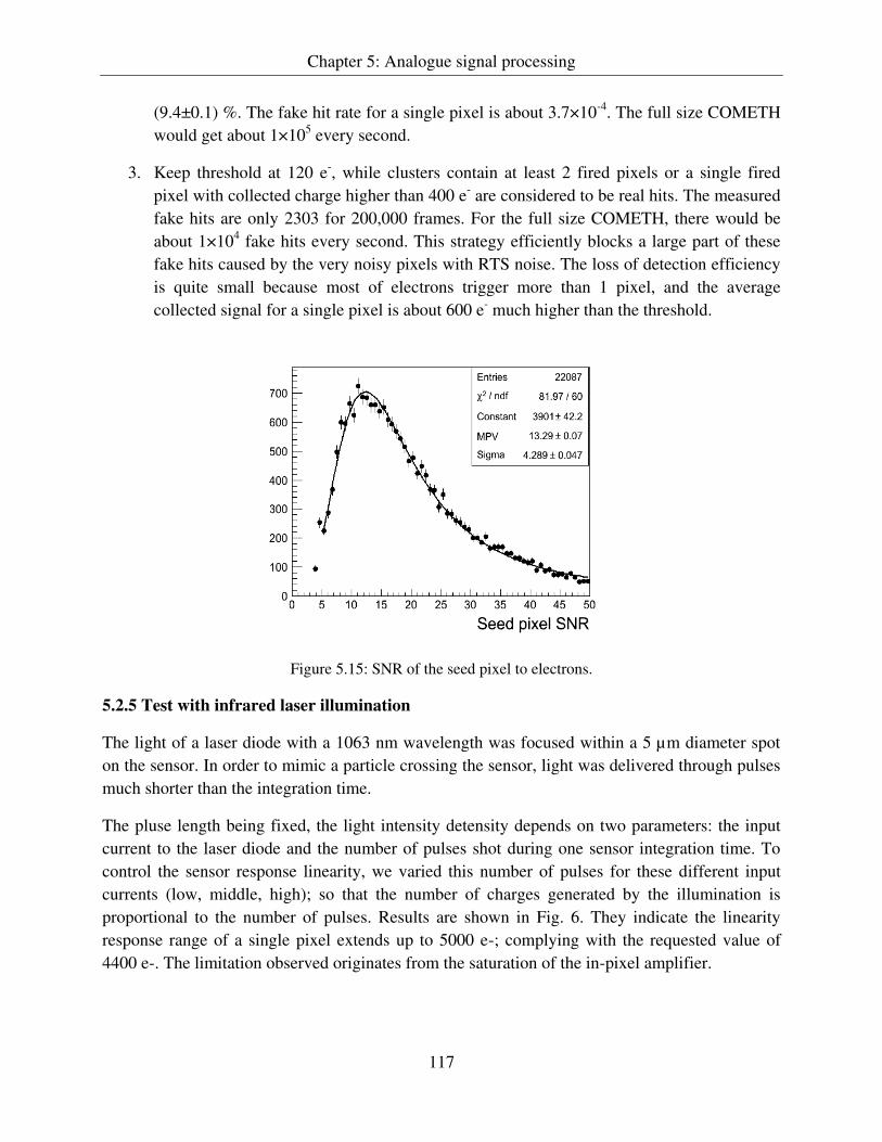
Chapter 5: Analogue signal processing
117
(9.4±0.1) %. The fake hit rate for a single pixel is about 3.7×10⁻⁴
. The full size COMETH
would get about 1×10⁵ every second.
3. Keep threshold at 120 e-, while clusters contain at least 2 fired pixels or a single fired
pixel with collected charge higher than 400 e- are considered to be real hits. The measured
fake hits are only 2303 for 200,000 frames. For the full size COMETH, there would be
about 1×10⁴ fake hits every second. This strategy efficiently blocks a large part of these
fake hits caused by the very noisy pixels with RTS noise. The loss of detection efficiency
is quite small because most of electrons trigger more than 1 pixel, and the average
collected signal for a single pixel is about 600 e- much higher than the threshold.
Figure 5.15: SNR of the seed pixel to electrons.
5.2.5 Test with infrared laser illumination
The light of a laser diode with a 1063 nm wavelength was focused within a 5 µm diameter spot
on the sensor. In order to mimic a particle crossing the sensor, light was delivered through pulses
much shorter than the integration time.
The pluse length being fixed, the light intensity detensity depends on two parameters: the input
current to the laser diode and the number of pulses shot during one sensor integration time. To
control the sensor response linearity, we varied this number of pulses for these different input
currents (low, middle, high); so that the number of charges generated by the illumination is
proportional to the number of pulses. Results are shown in Fig. 6. They indicate the linearity
response range of a single pixel extends up to 5000 e-; complying with the requested value of
4400 e-. The limitation observed originates from the saturation of the in-pixel amplifier.

Chapter 5: Analogue signal processing
118
However, in space the sensing diode may collect much more than 5000 e-, especially from low
energy protons. To test the pixel’s fast reset and recovery efficiency from such large signals, the laser was tuned to a very large intensity with various pulses frequencies. Results showed no
remnant signals in the frame just after the one having collected charges in excess of 5000 e-. This
test confirms the ability of the sensor to handle large signals.
Figure 5.16: Evolution of the pixel response to a linear increase of the laser illumination, for three
different laser currents. The laser illumination amplitude depends linearly on the number of laser pluses
shot during one sensor frame.
5.3 Conclusion and perspectives
A quarter-size prototype of our proposed CMOS pixel sensor for high-flux radiation counter has
been designed and fabricated in a 0.35 µm process. Tests of the pixel matrix corroborate the
expectation from previous simulations on the key parameters: charge collection efficiency,
detection efficiency for minimum ionizing particles, cluster size of a few pixels, and linearity
over the expected signal range.
Meanwhile, the tested noise is 30 e- which is higher than < 20 e
- reported by other sensors with
similar pixel architecture [1, 2]. The main reason is its relative low CVF (~ 33 µV/e-) comparing
with the 50 – 70 µW/e- CVF pixel in the references. Increasing the gain of the CS stage,
decreasing the capacitance value of the sensing diode, and optimizing the layout to reduce the
parasitic capacitance value on the path between sensing diode and the input transistor of the CS
stage are all effective methods to increase the CVF.
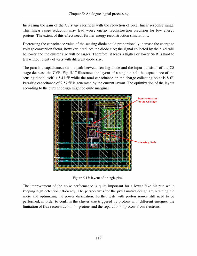
Chapter 5: Analogue signal processing
119
Increasing the gain of the CS stage sacrifices with the reduction of pixel linear response range.
This linear range reduction may lead worse energy reconstruction precision for low energy
protons. The extent of this effect needs further energy reconstruction simulations.
Decreasing the capacitance value of the sensing diode could proportionally increase the charge to
voltage conversion factor, however it reduces the diode size; the signal collected by the pixel will
be lower and the cluster size will be larger. Therefore, it leads a higher or lower SNR is hard to
tell without plenty of tests with different diode size.
The parasitic capacitances on the path between sensing diode and the input transistor of the CS
stage decrease the CVF. Fig. 5.17 illustrates the layout of a single pixel; the capacitance of the
sensing diode itself is 5.43 fF while the total capacitance on the charge collecting point is 8 fF.
Parasitic capacitance of 2.57 fF is generated by the current layout. The optimization of the layout
according to the current design might be quite marginal.
Input transistor
of the CS stage
Sensing diode
Figure 5.17: layout of a single pixel.
The improvement of the noise performance is quite important for a lower fake hit rate while
keeping high detection efficiency. The perspectives for the pixel matrix design are reducing the
noise and optimizing the power dissipation. Further tests with proton source still need to be
performed, in order to confirm the cluster size triggered by protons with different energies, the
limitation of flux reconstruction for protons and the separation of protons from electrons.

Chapter 5: Analogue signal processing
120
Bibliography
[1] Hu-Guo C., et al. CMOS pixel sensor development: a fast read-out architecture with integrated
zero suppression. JINST 4 P04012 2009.
[2] D. Doering, et al. Noise performance and ionizing radiation tolerance of CMOS Monolithic
Active Pixel Sensors using the 0.18 µm CMOS process. JINST 9 C05051 2014.

121
Chapter 6
From analogue to digital
As discussed in section 4.2, column-level ADCs with 3-bit resolution are required to be
implemented in COMETH. Its sampling rate should be about 4.2 MS/s to match with the pre-
stage pixel processing speed. In fact, a number of techniques for doing analog to digital
conversion could meet such speed and resolution specifications as illustrated in figure 6.1. This
chapter is going to start with the descriptions of ADC architectures which could be used in
COMETH application; then the design details of the chosen architecture with the most
advantages for this application are introduced; finally the prototype test results are discussed and
new architectures are proposed.
Sigma-Delta
SAR
Pipleline
Flash
Pipleline with
Interleaving
0.1 0.5 1 5 10 50 100 500 1000 2000
24
22
20
18
16
14
12
10
8
Sampling Rate (MHz)
Res
olu
tion
(b
its,
~S
NR
)
Figure 6.1: ADC architecture vs Resolution and sampling rate [1].

Chapter 6: From analogue to digital
122
6.1 Standard ADC architectures
Much research has been done on the implementation of analog to digital converters (ADCs). As a
result, a number of techniques for doing analog to digital conversion have been developed. Three
main standard ADC types appropriate to this application are introduced in this section; while
others are are not discussed here. Following the brief introduction of their working principles,
their advantages and the limits are also presented.
6.1.1 Flash ADC
The flash ADC architecture, also known as a fully parallel architecture, is fundamentally the
fastest architecture. An n-bit flash ADC consists of an array of 2n-1 comparators and a set of 2
n-1
reference values; each of the comparators samples the input signal and compares the signal to one
of the reference values. Each comparator generates an output indicating whether the input signal
is larger or smaller than the reference assigned to that comparator. The outputs of comparators
are then coded by a binary encoder to generate N-bit digital code corresponding to the input
signal.
Input
(1/2N )VR
sampler
Encoder
Binary Output
B0
B1
Bn-2
Bn-1
(2/2N )VR
[(2N -2)/2N ]VR
[(2N -1)/2N ]VR
Figure 6.2: Architecture of an N-bit flash ADC.

Chapter 6: From analogue to digital
123
As seen from Fig. 6.2, the comparators all operate in parallel. Thus the conversion speed is
limited only by the speed of the comparator or the sampler. For this reason, the flash ADC is
capable of high speed. However, two primary drawbacks to the flash ADC are the high power
dissipation and sensitivity to comparator offsets, as 2n-1 comparators are required.
6.1.2 Pipelined ADC
A pipelined ADC is also called sub-ranging quantizer; it uses two or more stages of sub-ranging.
A sample and hold circuit and an amplifier are added to each stage. The sample and hold circuit
is used by the first stage to sample the input. Subsequent stages use a sample and hold to sample
the residue from the previous stage. This feature allows each stage of the pipeline to begin
processing a new sample as soon as its residue is sampled by the following stage. Thus, the
throughput rate is independent of the number of stages in the pipeline. Because of this feature,
pipelined ADC can generally operate at very high sampling rates.
∑ Gain=2n
ADC DAC
Sample/hold
Vi Vo
n bits out
Cs Amplified
analog
redidue
inputSTAGE0 STAGE1 STAGE N-1
latch ∑ latch ∑
Analog pipeline
Digital pipeline Digital output
n output bits per stage
Figure 6.3: Block Diagram of a Typical Pipelined ADC.
The amplifier is used to amplify the residue before passing it on to the next stage. The resolution
requirements for the following stages are relaxed by adding this amplifier. Thus, the comparator
in the last stage of the pipeline does not need to be accurate to the full ADC resolution as it is
required in other sub-ranging ADCs [2]. Furthermore, comparator mismatches can easily be
eliminated as a limitation to resolution by self-calibration techniques. However, these gain blocks
in each stage tend to be the dominant source of power dissipation in the ADC.

Chapter 6: From analogue to digital
124
Because of their tolerance to comparator offsets and the ability of the pipeline stages to operate in
parallel, pipelined ADCs are well suited for high resolution applications where high speed is
required.
6.1.3 Successive approximation ADC
A successive approximation ADC uses a DAC to successively produce an analog reference signal
that approximates the input voltage signal. By adjusting the DAC until the reference signal
matches the input signal, a digital code representing the analog input is generated. In general, it
consist a sample-and-hold (S/H) circuit, a comparator, a Successive-Approximation-Register
(SAR) and a Digital-to-Analog Converter (DAC) as shown in Fig. 6.4.
Vin
SAR Register
Binary Output
B0B1Bn-2Bn-1
N-bit DAC
S/H
Figure 6.4: Basic architecture of an N-bit successive approximation ADC.
The S/H circuit is used to acquire the input voltage; it could convert a continuous time input
signal into a discrete time signal. The SAR and the DAC work together. The DAC converts the
corresponding digital code of SAR, which is dependent on the response of the comparator, into a
certain analog reference. This reference will be compared with the input signal and their
difference decides the following operation of the ADC.
The SAR applies a binary algorithm to search the closest digital code to match the input signal.
Instead of counting up in binary sequence, the SAR counts by starting with the Most-Significant
Bit (MSB) and finishing at the Least-Significant Bit (LSB). Firstly, after the initial reset, the
MSB is “1” and the others are “0”. It forces the DAC output to be ½ Vref which is half of the full-
scale range (FSR) of the ADC. This value is compared with the analog input signal. If the input
signal value is bigger, the MSB remains at “1”, otherwise it is set to “0”. The MSB is then
determined. The same process is repeated bit by bit until the LSB. Throughout the count process,
the register monitors the comparator’s output to see if the binary count is less than or bigger than
the input signal, adjusting the bit values accordingly. An example of the searching process of a 4-
bit SAR conversion is shown in the figure 6.5.
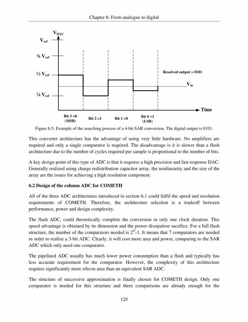
Chapter 6: From analogue to digital
125
VDAC
Time
Vin
¼ Vref
½ Vref
¾ Vref
Vref
Bit 3 =0
(MSB)Bit 2 =1 Bit 1 =0
Bit 0 =1
(LSB)
Resolved output = 0101
Figure 6.5: Example of the searching process of a 4-bit SAR conversion. The digital output is 0101.
This converter architecture has the advantage of using very little hardware. No amplifiers are
required and only a single comparator is required. The disadvantage is it is slower than a flash
architecture due to the number of cycles required per sample is proportional to the number of bits.
A key design point of this type of ADC is that it requires a high precision and fast response DAC.
Generally realized using charge redistribution capacitor array, the nonlinearity and the size of the
array are the issues for achieving a high resolution component.
6.2 Design of the column ADC for COMETH
All of the three ADC architectures introduced in section 6.1 could fulfil the speed and resolution
requirements of COMETH. Therefore, the architecture selection is a tradeoff between
performance, power and design complexity.
The flash ADC, could theoretically complete the conversion in only one clock duration. This
speed advantage is obtained by its dimension and the power dissipation sacrifice. For a full flash
structure, the number of the comparators needed is 2N-1. It means that 7 comparators are needed
in order to realize a 3-bit ADC. Clearly, it will cost more area and power, comparing to the SAR
ADC which only need one comparator.
The pipelined ADC usually has much lower power consumption than a flash and typically has
less accurate requirement for the comparator. However, the complexity of this architecture
requires significantly more silicon area than an equivalent SAR ADC.
The structure of successive approximation is finally chosen for COMETH design. Only one
comparator is needed for this structure and three comparisons are already enough for the

Chapter 6: From analogue to digital
126
complete conversion of a 3-bit ADC. According to the size of this architecture, the capacitor
array needed can be successfully implemented in a space of 50 µm width because only 3-bit
resolution is required. As a result, the speed and resolution requirements can be achieved by very
lower power dissipation, small silicon area and simple architecture.
Based on the previous simulations and measured pixel response to electron particles, the expected
transfer function of the ADC is shown in figure 6.6. The “threshold” (Vth) value for the first bit
was set at 120 e- for high detection efficiency close to 100%. The step size (VLSB) between two
adjacent bits corresponds to 700 electrons collected on the sensing diode.
Digital
Output
111
110
100
011
010
001
101
000
VLSB(700e-) 2VLSB 3VLSB 4VLSB 5VLSB 6VLSB 7VLSB
Expected Characteristic
Vth
120 e-
820 e-
1520 e-
2220 e-
2920 e-
3620 e-
4320 e- Charge collected
Figure 6.6: Expected transfer function of the 3-bit ADC in COMETH.
6.2.1 Global architecture and processing principle
To meet the expected transfer function, figure 6.7 shows the proposed global ADC structure
including a S/H circuit, a DAC, a comparator and a Finite-state machine (FSM) which performs
the SAR logic.

Chapter 6: From analogue to digital
127
Vr1Vtc
Vr1
Vdr
Vr2
SH2
SH1
S_tcS_tcb
SET
SET
FSM
Control logic
results
Sample & holdVpix
C C/2 C/4 C/4
DAC
Comparator
Chip-level control logic
CL
Figure 6.7: Global architecture of the column 3-bit SAR ADC for COMETH.
Signal levels from pixel output are maintained by the sample-and-hold block every comparison.
The DAC is realized by capacitor array consisting of binary weight capacitors which correspond
to the different bits of the digital code. The total capacitance of the array is 2C (C = 200 fF in this
design). A switch array is connected to the capacitors to select the different terminals. Therefore,
different references values corresponding to different bits can be generated during the conversion
based on the charge redistribution principle. The global commands (reset, SH1, SH2, clock for
FSM) are common to all the columns and are sent by chip level control logic. Column level
control logic is integrated in the FSM inside each column, transferring the serial switch select
signal and making the decision according to the response of the column level comparator. The
comparator compares the signal value maintained by the S/H circuit with the reference value
generated by the DAC and gives the logic response to the FSM for making the decision.
In the Fig. 6.7, Vr1 is the common mode of the comparator’s input, together with Vdr defines the
full-scale range (VLSB = − / ), Vtc and Vr2 are used to set the threshold value and tune
the ADC offset externally. So the ADC transfer function could shift as the expected curve in
figure 6.6. The ADC has a 3-bit precision but a 4-bit output. An extra bit is used to show if the 3-
bit data is equal to “000” or not. This extra bit is used for the following digital processing block which will be introduced in Chapter 7.

Chapter 6: From analogue to digital
128
SH1
SH2
SET
S_tc
rstADC
240 ns
ClkADC
60 ns
Figure 6.8: Timing diagram for the column 3-bit SAR ADC.
Compared with typical SAR ADC introduced in section 6.1.3, this design adds a “sleep” mode which is realized by an extra comparison before the analog to digital conversion; the
discrimination threshold is tuneable externally n order to adjust the detection sensitivity. When
this first comparison fails, the ADC turns itself off until the next sample. The strategy reduces the
time left for each comparison, increases the power dissipation for the conversion of a signal
higher than threshold. However, it allows taking advantage of the low occupancy of the matrix
(more than 97% of the pixels are unfired up to flux as high as 107 particles·cm
-2·s
-1) in order to
significantly limit the system power dissipation. Figure 6.8 displays the timing diagram and its
operation proceeds as follows:
1) Firstly, after the reset (rstADC), during the SET phase, the signal value with offset VSH1
and the offset value VSH2 of the S/H block will be sampled and stored respectively (VSH1 − VSH2 is the signal value free from offset). The offset value is memorized on the
capacitor CL and the signal value is memorized on the capacitor array. The other side of
the capacitors array and CL are set to Vr2 and Vr1 respectively. The equivalent circuit is
showed in Fig. 6.9 below.
VSH1
Vr2
Vr1
C C/2 C/4 C/4
ComparatorCLVSH2
Figure 6.9: Equivalent ADC circuit during the SET phase.
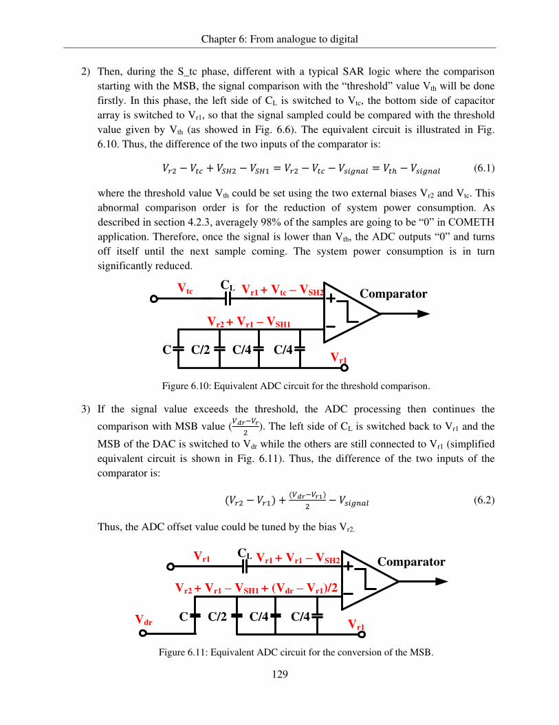
Chapter 6: From analogue to digital
129
2) Then, during the S_tc phase, different with a typical SAR logic where the comparison
starting with the MSB, the signal comparison with the “threshold” value Vth will be done
firstly. In this phase, the left side of CL is switched to Vtc, the bottom side of capacitor
array is switched to Vr1, so that the signal sampled could be compared with the threshold
value given by Vth (as showed in Fig. 6.6). The equivalent circuit is illustrated in Fig.
6.10. Thus, the difference of the two inputs of the comparator is: − + − = − − = ℎ − (6.1)
where the threshold value Vth could be set using the two external biases Vr2 and Vtc. This
abnormal comparison order is for the reduction of system power consumption. As
described in section 4.2.3, averagely 98% of the samples are going to be “0” in COMETH application. Therefore, once the signal is lower than Vth, the ADC outputs “0” and turns off itself until the next sample coming. The system power consumption is in turn
significantly reduced.
Vr1
Vr2 + Vr1 – VSH1
Vr1 + Vtc – VSH2
C C/2 C/4 C/4
ComparatorCLVtc
Figure 6.10: Equivalent ADC circuit for the threshold comparison.
3) If the signal value exceeds the threshold, the ADC processing then continues the
comparison with MSB value (−
). The left side of CL is switched back to Vr1 and the
MSB of the DAC is switched to Vdr while the others are still connected to Vr1 (simplified
equivalent circuit is shown in Fig. 6.11). Thus, the difference of the two inputs of the
comparator is: − + − − (6.2)
Thus, the ADC offset value could be tuned by the bias Vr2.
Vr1
Vr2 + Vr1 – VSH1 + (Vdr – Vr1)/2
Vr1 + Vr1 – VSH2
C C/2 C/4 C/4
ComparatorCLVr1
Vdr
Figure 6.11: Equivalent ADC circuit for the conversion of the MSB.

Chapter 6: From analogue to digital
130
4) The following comparison processes are just the same with a typical SAR ADC as
described in section 6.1.3. The final 3-bits digital value will be ready after 2 more
conversions. It takes 30 ns for one conversion and the time needed for a whole successive
approximation process, in addition of SET and reset phase, is 240 ns, exactly matches
with the pixel analogue processing time.
6.2.2 Design of the S/H circuit
Normally, the sample and hold circuit is used to sample the voltage of a continuously varying
analog signal and holds its value at a constant level for a specified minimum period of time.
However, in COMETH application, the signals from pixels are constant levels already. Instead of
capturing and freezing the value of a continuously varying analog signal at a certain moment, the
S/H circuit used here takes two other responsibilities. The first one is doing the subtraction,
getting the “useful signal” for the subsequent comparisons with DAC provided references. This
“useful signal” refers to − introduced in section 5.1, is the signal absolute value free
from the diode reset noise, offset of the pre-amplify stage and the SF stage. The second one is
acting as a buffer stage between pixel processing and the digitization stage. For the continuous
processing of the system, the S/H circuit needs to start processing the signal from one sample
while its provided “useful signal” of last sample is still being digitized by its following circuit.
The sampling techniques are broadly classified in two methods: parallel sampling and series
sampling [3, 4], as presented in Fig. 6.12.
CHS2Vin X Vout
Vref
S1
S3
CpCH
S1Vin X Vout Y
(a) (b)
Figure 6.12: Sampling structure: (a) parallel sampling, (b) series sampling.
In the circuit of Fig. 6.12 (a), the sampling capacitor is in parallel with the signal, and the input
and the output are DC-coupled. In the acquisition mode, S1 is turned on for the voltage of the
sampling capacitor CH (point x) to track the level of the input signal and it is turned off in the
transition to the hold mode.

Chapter 6: From analogue to digital
131
In the circuit of Fig. 6.12 (b), the sampling capacitor is in series with the signal, thereby isolating
the common-mode (CM) levels of the input and the output. During the acquisition mode, S2 and
S3 are on and S1 is off, sampling the input signal on CH. In the transition to the hold mode, S3 is
firstly turned off to release node Y from Vref; and then subsequently S2 is turned off while S1 is
turned on to short point X to ground, producing a voltage change equal to the input voltage at the
output.
The series sampling structure has several advantages over the parallel sampling structure. Besides
isolated input and output CM levels, the series sampling structure does not suffer from input-
dependent switch charge injection errors. S3 turns off before S2, and the gate voltage applied on
S3 is constant (Vref), thus injecting a constant charge onto node Y. This error can be eliminated
through differential operation.
With respect to the parallel structure, the series structure also has two disadvantages. The first
one is that the nonlinearity of the parasitic capacitance Cp at point Y introduces distortion in the
sampled value. This effect can be attenuated by using a large value CH. The other one is it takes
longer time for the sampling level to settle than in the parallel sampling structure. Because its
output voltage always begins from the reset value (Vref) for every sample whereas in parallel
sampling structure the output voltage begins from a level close to its final value. .
Vr
CH1
CH2 CL2
SH2_out
SH1_out
CL1
S1 (Read)
S2 (Calib)
S4 (SH2)
S3 (SH1)
Vin_pix Buffer
S1 (Read)
S4 (SH2)
X
Y
Figure 6.13: Schematic of the S/H circuit.
In this design, the two sampling techniques are combined to take both their advantages. Figure
6.13 represents the schematic of the S/H circuit. The circuit consists of four capacitors, an output
buffer and six switches. Vr is the input reference level of the buffer. The small value (100 fF)
parallel sampling capacitor CH1 is used for fast sampling the pixel signal and memorizing the
pixel output reference level. The large value (350 fF) series capacitor CH2 isolates the CM levels
of the signal from pixel and the signal provided to digital conversion. Due to the signal after
sampling is provided to the DAC which is a capacitor array, the buffer is used here to guarantee

Chapter 6: From analogue to digital
132
the speed of signal transition. In addition, after doing the signal subtraction ( − , two
more capacitors are required (CL1 and CL2). CL1 is used for memorizing the signal level after
subtraction ( − , while CL2 is used for memorizing the offset level of the buffer.
S1 (Read)
S2 (Calib)
Fck = 100 MHz
S4 (SH2)
S3 (SH1)
Figure 6.14: Timing diagram of the S/H circuit.
The circuit is then functioned with proper timing control of the six switches. The timing diagram
is represented in figure 6.14. The switches S1 and S2 use the signals Read and Calib (Chapter 5).
The switches S3 and S4 are controlled by signal SH1 and SH2 of the ADC, respectively. The
detailed procedure is following:
1) At first, the pixel output signal (Vread: signal of charged particle with offset) is sampled. S1
is turned on and the pixel output signal is sampled both on CH1 and CH2. Then, CH1 and
CH2 are disconnected from the pixel and the signal level is memorized on both of the
capacitors. In this step, the voltage level at point X equals to Vread, and the voltage level at
point Y equals to Vr.
2) Secondly, the pixel output reference level with offset (Vcalib) is sampled and subtracted
from Vread. S2 is firstly turned on, making the voltage level at point X equal to the pixel
output value (Vcalib). Comparing to the first step, the voltage change at point X is | −|. The voltage level at point Y tracks the voltage change of the point X. Therefore, at
this moment, the voltage level of point Y is the difference of the reference value Vr and
the “useful signal” value − . This is the useful signal free of offset due to
the pixel output stage. Then, S3 is activated and the useful signal, slightly attenuated by
the gain of the buffer, is stored on CL1. S3 is turned on after S2 in order to wait for the end
of the offset cancellation operation.
3) In the end, S4 is turned on, sampling and storing the offset value of the buffer on CL2.
After all the above three steps, the difference between the samples stored on CL1 and CL2 (VSH1 –
VSH2) is the real signal value of the charged particle, free from all the offsets (both the pixel
output stage and the S/H circuit).

Chapter 6: From analogue to digital
133
Vin
Vout
Vbias M5
M3
M2M1
M4
25 nsOut
In
(a) (b)
Gain Vout
1 V
(c)
Figure 6.15: Schematic of the unit gain buffer (a); its transient response (b) and static response (c).
Since the concerned input signal value range from the pixel output is close to 1 V (Fig. 5.5), no
further amplitude is implemented in this S/H stage. A unit gain buffer is chosen to driven the
following capacitor array. Its schematic and simulated responses are given in Fig. 6.15.
According to Fig. 6.15 (c), the static gain is about 0.96 when the input common mode is around
1.5 V. Using this common mode value, its transient response with an input signal equaling to 1 V
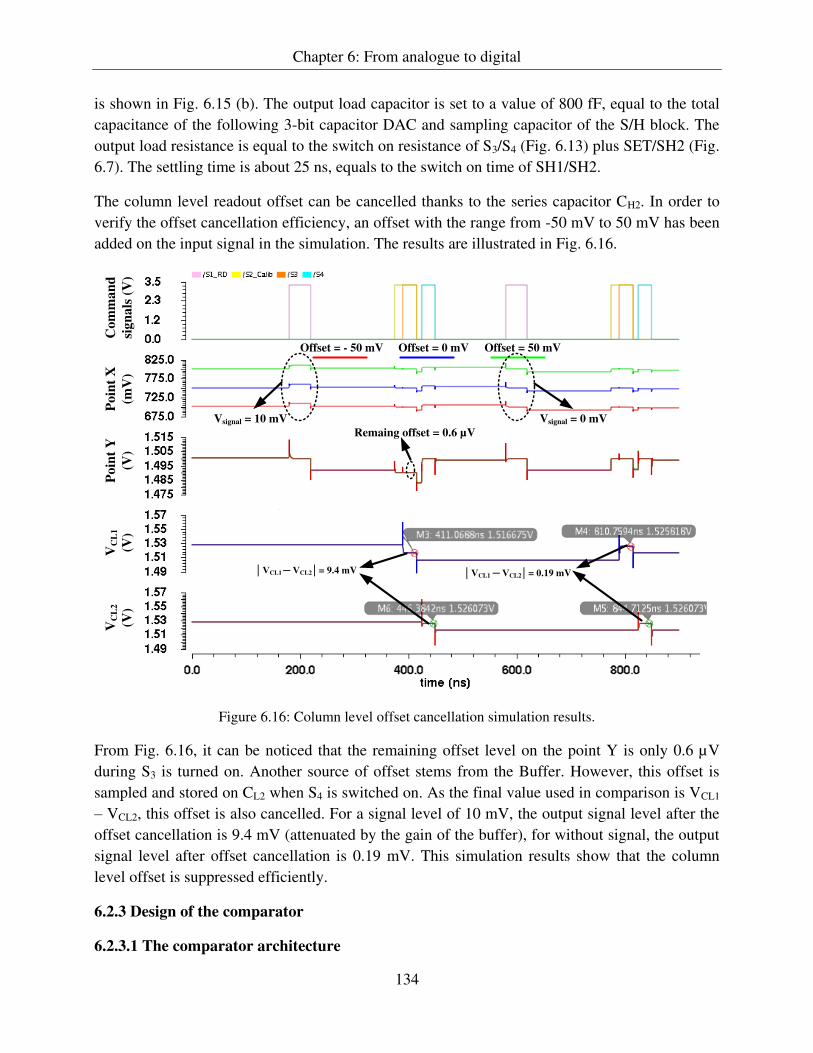
Chapter 6: From analogue to digital
134
is shown in Fig. 6.15 (b). The output load capacitor is set to a value of 800 fF, equal to the total
capacitance of the following 3-bit capacitor DAC and sampling capacitor of the S/H block. The
output load resistance is equal to the switch on resistance of S3/S4 (Fig. 6.13) plus SET/SH2 (Fig.
6.7). The settling time is about 25 ns, equals to the switch on time of SH1/SH2.
The column level readout offset can be cancelled thanks to the series capacitor CH2. In order to
verify the offset cancellation efficiency, an offset with the range from -50 mV to 50 mV has been
added on the input signal in the simulation. The results are illustrated in Fig. 6.16.
Offset = 50 mVOffset = 0 mVOffset = - 50 mV
Vsignal = 10 mV Vsignal = 0 mV
Remaing offset = 0.6 µV
│VCL1 ─ VCL2│= 9.4 mV │VCL1 ─ VCL2│= 0.19 mV
Co
mm
an
d
sig
na
ls (
V)
VC
L1
(V)
Po
int
X
(mV
)
Po
int
Y
(V)
VC
L2
(V)
Figure 6.16: Column level offset cancellation simulation results.
From Fig. 6.16, it can be noticed that the remaining offset level on the point Y is only 0.6 µV
during S3 is turned on. Another source of offset stems from the Buffer. However, this offset is
sampled and stored on CL2 when S4 is switched on. As the final value used in comparison is VCL1
– VCL2, this offset is also cancelled. For a signal level of 10 mV, the output signal level after the
offset cancellation is 9.4 mV (attenuated by the gain of the buffer), for without signal, the output
signal level after offset cancellation is 0.19 mV. This simulation results show that the column
level offset is suppressed efficiently.
6.2.3 Design of the comparator
6.2.3.1 The comparator architecture

Chapter 6: From analogue to digital
135
As Fig. 6.17 illustrated, a typical comparator architecture utilized in A/D converters consists of a
preamplifier A1 and a latch and has two modes of operation: tracking and latching [5]. In the
tracking mode, A1 is enabled while the latch is disabled. The input difference value is amplified
and “tracked” by the preamplifier A1. In the latching mode, A1 is disabled and the latch is enabled
so that the instantaneous output of A1 is amplified and logic levels are produced at Vout.
VoutA1 Latch
Vin1
Clk
Vin2
Figure 6.17: Typical comparator architecture.
The minimum resolvable input voltage of this architecture is limited by the offsets of MOS
devices. The large mismatches of MOS devices makes it is mandatory to use offset cancellation
in the comparator design for the high precision systems. There are varieties of comparator offset
cancellation techniques [6, 7]; their architectures are similar to Fig 6.17, but have three modes of
operation: offset cancellation, tracking and latching. Two of these techniques are widely used: the
IOS (Input Offset Storage) and the OOS (Output Offset Storage).
Clk
Vout
C1
C2
A1
S3
S4
S1
S2
S6
S5
LatchVin
A
B
P
Q
X
Y
Figure 6.18: Input offset storage architecture.

Chapter 6: From analogue to digital
136
Fig. 6.18 depicts the configuration of the IOS technique. During the offset cancellation mode, S1-
S4 are switched on, S5-S6 are off, thus nodes A and B are grounded, a unit-gain feedback loop is
established around the preamplifier A1, and the input offset is stored on C1 and C2. During the
tracking mode, S1-S4 are off, S5-S6 are switched on, the feed-back loop is open, and A1 senses the
analog input and amplifies the difference. In the latching mode, the latch is strobed so as to
regenerative amplify the difference produced at the preamplifier output, hence providing logic
levels at Vout.
The residual offset (the offset after cancellation) of this topology is given by [6, 7]: = + + ∆ + � (6.3)
Where Vos(tot) is the total offset value, VOSA and VOSL are the offset of the amplifier and the latch
respectively, A1 is the gain of amplifier, ∆ is the charge injected mismatch between switch S3
and S4, and C is the value of C1 and C2 (assumed equal here). Thus, IOS reduces the effect of the
preamplifier and latch offsets by approximately a factor of A1.
The IOS achieves a wide input range, however it features a large input capacitance and its offset
cancellation ability requires a high gain, degrading the power-speed trade-off.
Clk
Vout
C1
C2
A1
S3S1
S2
S6
S5
LatchVin
A
B
X
Y
S4
Figure 6.19: Output offset storage architecture.
The IOS technique measures the input offset of the preamplifier by closing a unity-gain feedback
loop around it and stores the resulting offset on capacitors in series with the input. While the
OOS technique measures the output-referred offset of the preamplifier by grounding its inputs

Chapter 6: From analogue to digital
137
and stores the result on capacitors in series with the preamplifier output. Illustrated in Fig. 6.19,
the OOS architecture operates as follows.
During the offset cancellation mode, S1-S4 are switched on, S5-S6 are off, thus nodes A, B, X, and
Y are grounded and the preamplifier offset is amplified and stored on C1 and C2. During the
tracking mode, S1-S4 are off, S5-S6 are switched on. The signal is sampled and the offset is
automatically corrected. Finally, in the latching mode, the latch is strobed to amplify its input
voltage and produce logic levels at Vout. The total residual input referenced offset is [6, 7]: = ∆ + � (6.4)
Where ∆ is the charge injected mismatch between S3 and S4. In contrast with IOS, the offset of
the preamplifier is completely canceled, and the effect of charge injection mismatch is divided by
A1. In addition, OOS exhibits less input capacitance than IOS.
There are two main drawbacks of this architecture. Firstly, a high gain amplifier can not be used
to avoid the possible amplifier output saturation during the offset cancellation mode. As a
consequence, OOS typically incorporates a single-stage amplifier with a gain less than 20 [7].
Secondly, contrast with IOS where rail-to-rail inputs can be accommodated; input DC-coupling
limits the input common-mode range of this structure.
Due to the potentially lower offset and less input capacitance than IOS structure; the OOS
technique is finally chosen for this design. Its schematic and timing are represented in Fig. 6.20.
Clk
Vop
C0Amplifier
Offsetcancel
Latch
Vinp
Vinn
Vref
Vref Vref
Vref
Buf
Buf
En_amp
Offsetcancel
Offsetcancel Offsetcancel
Offsetcancel
Offsetcancel Von
S
R
Q
Qn
Rst
RstADC
Comp_result
(a)

Chapter 6: From analogue to digital
138
Offsetcancel
Offsetcancel
Clk_latch
(b)
Figure 6.20: The architecture (a) and its operation timing (b).
The differential inputs of the preamplifier are provided by S/H circuit and DAC, as introduced in
section 6.2.1; these values are stored on the capacitors and very sensitive to the kickback noise of
the comparator [8]. Therefore, two buffers are added in the front of the preamplifier to mitigate
the kickback noise. The so called kickback noise is due to the large voltage variations in the
internal nodes of the comparator; they are coupled through the parasitic capacitances of the
transistors to in the comparator input and disturbing the input voltage.
6.2.3.2 The preamplifier
Vin+
En_amp
Vin-Vout-Vout+
M2
M3
M4
M1: 10 µm/0.5 µm M1
M2: 0.6 µm/0.6 µm
M3: 10 µm/0.4 µm
Ib1: 70 µA
Ib2: 25 µA Ib2
VddStage 2 Stage 2
Stage 1
Figure 6.21: schematic of the preamplifier used in the comparator.
To obtain reasonable gain, speed and effectively reduce the kickback noise [8], two stages are
employed in the preamplifier. As illustrated in figure 6.21, stage 1 is a differential NMOS input

Chapter 6: From analogue to digital
139
pair with diode-connected loads, and stage 2 is two PMOS source followers with no body effect
[9]. A switch signal En_amp provided by the FSM is used to switch off the bias current Ib1 when
appropriate, so as to increase the power efficiency. This appropriate occasion is right after the
first comparison of each sample when the signal value is less than the threshold value. The power
savings are proportional to the amount of time that the preamplifier is disabled and the amount of
pixels have been fired each frame. For a single sample conversion, the amplifier either need to be
switched on for only one comparison (30 ns) or all the four comparisons (30 ns × 4). Because the
full conversion time of each sample is 240 ns, the power consumption of the amplifier will be
~280 µW for the case with signal and ~ 194 µW for the case without signal (Equation 6.5 and
6.6). µ × × + µ × × . ≈ µ (6.5) µ × + µ × × . ≈ µ (6.6)
The gain of the amplifier is mainly determined by the first stage and the second stage is used to
improve the speed. According to the simulation, the global gain is 8.3 and the -3dB bandwidth is
120 MHz with 100 fF load (C0).
6.2.3.3 The dynamic latch
Vin+
Vbias
M1
Latch
Vin-
Vout-
M2
M3 M4
M5 M6M7 M8
M9
M10
Latch Latch
Vdd
Vout+S
R
Q
QnRst
RstADC
Comp_result
Cross-coupled inverters
X
Y
Cpx Cpy
Flip-flop
Latch
2Id
Id - Id +
W/L (µm):
M1 : 25/1.5
M3 : 2.5/0.5
M5 : 5/0.5
Figure 6.22: Schematic of the dynamic latch.
A dynamic latch offers good speed and no-static power dissipation shown in figure 6.22 is
implemented in this design. It is a modification of the one proposed in [10]. M1 – M2 are the input

Chapter 6: From analogue to digital
140
devices, M3 – M6 form the two cross coupled inverters acting as regenerative loads, M7 – M9 are
switches, and M10 is biasing current source. Two additional inverters are used to balance the
charges seen by the outputs of the latch. The latch outputs are finally loaded by a flip-flop.
When the “Latch” signal is low (resetting phase), the NMOS transistor M9 prevents the static
current flow; PMOS transistors M7 – M8 conduct and charge the parasitic capacitances (Cpx and
Cpy) at point X and Y with the high potential “Vdd”. Thus, the latch outputs are reset to low. Once
the “Latch” signal goes high, M9 conducts and M7 – M8 are switched off. The differential inputs
cause different branch currents through M1 and M2, so the parasitic capacitors (Cpx and Cpy) at
point X and Y discharge with different speed which leads to a potential difference between point
X and Y. Subsequently, M3 – M6 amplify VXY to rail-to-rail levels.
The input offset voltage of this architecture can be expressed as [11]: = ∆ , + − , (∆ / ,/ , + ∆ �� ) (6.7)
Where ∆ , is the threshold voltage mismatch of the input devices M1 and M2, − ,
is the overdrive voltage of the input differential pair, ∆ / , is the physical dimension
mismatch between M1 and M2, and ∆ is the load resistance mismatch introduced by M3 – M6.
The first term on the right side of (6.7) stems from threshold mismatch which is a bias-current
independent constant value. It is a strong function of process cleanliness and uniformity and can
be substantially improved by a careful layout. The second term scales with the overdrive voltage
and the device W/L ration. Therefore the offset of the dynamic latch can be reduced by enlarging
the size of the input transistors and reducing their overdrive voltages. However, large input
device size introduces large parasitic capacitor Cp, which decreases the gain of the preamplifier
by a factor of +⁄ . To reduce the input overdrive voltage, a biased MOS transistor M10
is cascaded at the bottom to control the tail current.
The Monte Carlo simulation indicates this dynamic latch has an offset of around 1.6 mV (mean
value) with 3.2 mV standard deviation. Divided by the gain of the preamplifier stage, the input
referenced offset component contributed by the latch to the comparator is only around 0.2 mV
(equation 6.4).
6.2.4 Layout and estimated power dissipation
The column level SAR control logic are described using the hardware description language
Verilog and synthesized within a 200 µm × 50 µm layout area. Figure 6.23 represents the layout
of a single ADC. Its width is matched with the pixel pitch size; and its total length is about 850
µm including some switch blocks added for testability. The designed conversion period is 240 ns
and estimated power consumption is about 550 µW with signal and 750 µW without signal (with
3.3 V power supply).

Chapter 6: From analogue to digital
141
FSM
200 µm 185 µm 315 µm 115 µm
50 µm
Comparator DAC S/H circuit
Figure 6.23: layout of the column-level ADC.
6.3 Test of the column level ADC
The reduced scale prototype contains 32 column ADCs. To determine their performances, pixel
array is isolated and its output in Read and Calib phase were replaced by two external voltage
references Vtest1 & Vtest2. The full signal range was split into 300 identical steps. An average of
320 events has been calculated for each step. Its expected LSB is 700 e- corresponding to 23.1
mV taking into account the pixel CVF measured previously.
The ADC power dissipation is also measured to 532 and 759 µW with an input signal
respectively lower and higher than threshold respectively. These results confirm the power
efficient design due to the addition of the threshold comparison. Because most of the pixels are
unfired during the operation, the average ADC power dissipation would be very close to the low
power dissipation level without signal, for instance 539 µW/ADC with 3% fired pixels.
6.3.1 Characteristics of a single ADC
Ideal
ADC31
Figure 6.24: Transfer functions of ADC31 and the expected ideal one.
As described in section 6.2.1, the ADC transfer function could be adjusted by 4 external voltage
references: Vr1, Vr2, Vtc and Vdr. These four references are applied to all the columns. Before start
taking data of all the columns, for the purpose of choosing the suitable references for all the

Chapter 6: From analogue to digital
142
columns, the performance of ADC31 (the ADC of the most right column) are used to compared
with the ideal expected characteristic.
After the adjustment, a pretty good match of transfer function between ADC31 and the expected
ideal one is achieved which is displayed in Fig. 6.24. As shown in Fig. 6.25, the INL/DNL for
ADC31 are less than ±0.12 LSB.
(a) (b)
Figure 6.25: DNL (a) and INL (b) characteristics of ADC31.
6.3.2 Characteristics of the 32 columns
Figure 6.26: Transfer functions of the 32 column ADCs (enlarged LSB value).

Chapter 6: From analogue to digital
143
Fig. 6.26 displays the transfer functions of the entire 32 column ADCs. Although each ADC
keeps the same constant I/O characteristic, they suffer a significant dispersion between each
column which is so called the column fixed-pattern noise (FPN). Test results indicate the FPN
(rms) value is about 4.96 mV (0.21 LSB). Obviously, this value is too large and would be the
main feature needs to be improved in the next prototype. The unidentified ADC performances
would affect the reconstruction results which are going to be discussed in detail in section 7.3.
(a) (b)
Figure 6.27: Column dispersion of the first bit: (a) zoom of the 1st bit; (b) fixed pattern noise.
In the design of COMETH, offset compensate techniques have been employed in the following
blocks: pixel, S/H circuit and comparator. The offset of the ADC is mainly from the channel
charge injection of the switch transistors on the DAC capacitors. These charge injections
introduce errors to the two voltage levels used for comparisons. The quantity of this error is
directly proportional to the size of the switch transistor and inversely proportional to the value of
sampling capacitor, and could be expressed as [9]: ∆ ∝ � ��− − (6.8)
Where CH represents the value of the sampling capacitor, Vin is the potential needs to be sampled,
VTH is the threshold voltage of the transistor, Cox is the transistor bottom-plate junction
capacitance per unit area. In fact, the left side of equation 6.8 is the total charge in the inversion
layer of the transistor while it is conducted. A fraction of this value will be injected to the
sampling capacitor and create the error ∆ when the transistor is switched off.
For a single ADC transfer function, the offset caused by the channel charge injection could be
corrected. As described in section 6.2.1 and equation. 6.2, the ADC transfer function offset could
be adjusted by the difference of external bias Vr2 and the comparator commode mode reference
Vr1.

Chapter 6: From analogue to digital
144
The measured column FPN is caused by the uncertainty of ∆ for each column and a certain Vr2
for all the columns. Therefore, either reduce the maximum value of ∆ or provide differentiated
reference “Vr2” for each column is helpful to reduce this column FPN.
6.4 Solutions for the ADC performance improvement
Test results indicate the ADC column FPN noise is the key performance needs to be improved in
order to provide qualified data for the following digital processing logic. The solutions could be
reducing the quantity of channel charge injection (∆ ) or compensating this error by additional
references.
As equation 6.8 indicates, using a smaller size switch transistor and a bigger sampling capacitor
value could help obtaining a smaller charge injection error. However, this would consume more
power to realize the same speed and the error can still not be cancelled. Several other techniques
could also be used; such as addition of “dummy” device, using of complementary switches or differential sampling circuit [9], but each leading to other trade-offs.
Compensating the offset error by additional references is an effective method. The column ADC
designed for HMRM ASIC (Fig 6.28) employs an 8-bit trimming DAC to compensate the
comparator offset [12]. Each ADC has its own trimming register, and has to be calibrated
separately before acquiring data.
Figure 6.28: Overview of the ADC designed for the HMRM ASIC. An 8-bit trimming DAC compensates
the comparator offset [12].
Bring this compensation method to the ADC designed for COMETH, hypothesis a 6-bit
programmable “Vr2” with 1 mV resolution could be used to adjust the offset separately for each

Chapter 6: From analogue to digital
145
column. A much better noise results, 0.25 mV (0.01 LSB) FPN rms value, of the 32 columns
would be achieved as illustrated in figure 6.29.
Temporal Noise:
Vp-p ~ 4.5 mV
rms: ~ 0.52 mV
FPN (rms): ~ 0.25 mV
Norm
ali
zed
Resp
on
se
Vsignal (mV)
(a) (b)
Figure 6.29: Results with compensation: (a) transfer functions of 32 columns; (b) noise of the first bit.
However, adding a 6-bit DAC to each column ADC with just 3 bits resolution seems a waste of
hardware area. A column ADC designed for the CMOS vertex detector [13] brings another low
FPN idea for low resolution ADCs with advantages of low power and small area.
Figure 6.30: The column ADC architecture with Switched-DAC for comparator references [13].
The DAC used in Fig. 6.30 is not implemented with a capacitor array as the typical design. It is
implemented with a switch multiplexer with eight external references. The references for all the
ADCs are not generated in each ADC itself, they are provided for all the columns at the same

Chapter 6: From analogue to digital
146
time, it potentially reduces the diversity of ADC references thus the column FPN. This method is
especially attractive to low resolution column ADCs for small size sensors. High resolution ADC
would require a very large number of references (2n); large sensor size may lead to a significant
references voltage drop from side to side. Moreover, the removal of capacitor array release the
switch transistor size requirement and costs less power consumption for the same sampling rate.
The tested FPN rms value of this architecture is only 0.40 mV for a sensor width of 1680 µm. For
the full size COMETH with 3200 µm sensor width, with the same architecture, a FPN (rms)
slightly higher than 0.40 mV (0.017 LSB) can be foreseen.

Chapter 6: From analogue to digital
147
Bibliography
[1] Carmen Parisi. Tradeoffs in New-generation ADCs. EEWeb. Aug 22, 2011. Availably at:
http://www.eeweb.com/blog/carmen_parisi/balancing-the-tradeoffs-in-new-generation-adcs
[2] Andrew G. F. Dingwall and Victor Zazzu. An 8-MHz CMOS Subranging 8-bit A/D Converter.
IEEE J. Solid-State Circuits, vol. SC-20, no. 6, Dec. 1985, pp. 1138-1143.
[3] B. Razavi. Design of Sample-and-Hold Amplifier for High-Speed Low-Voltage A/D. IEEE 1997
Custom Integrated Circuits Conference, 1997.
[4] B. Razavi. Design of a 100-MHz 10-mW 3-V Sample-and-Hold Amplifier in Digital Bipolar
Technology. IEEE Journal of Solid-State Circuits, vol. 30, no. 7, pp. 724-730, July 1995.
[5] B. Razavi. Principles of Data Conversion System Design. IEEE Press, NY, 1995.
[6] D. J. Allstot. A Precision Variable Supply CMOS Comparator. IEEE J. Solid-State Circuits, vol.
SC-17, pp. 1080-1087, Dec. 1982.
[7] B. Razavi and B. A. Wooley. Design Techniques for High-Speed High Resolution Comparators.
IEEE J. Solid-State Circuits, vol. SC-27, PP. 1916-1926, Dec. 1992.
[8] Pedro M. Figueiredo, et al. Kickback Noise Reduction Techniques for CMOS Latched
Comparators. IEEE Transactions on circuits and systems. VOL. 53, NO. 7, July 2006.
[9] B. Razavi. Design of Analog CMOS Integrated Circuits. McGraw-Hill Companies, Inc. 2001.
[10] T. Kobayashi, et al. A current controlled latch sense amplifier and a static power-saving input
buffer for low-power architecture. IEEE J. Solid-State Circuits, vol. 28, pp. 523-527, Apr.
1993.
[11] P. R. Gray and R. G. Meyer. Analysis and Design of Analog Integrated Circuits. Third Edition,
John Wiley and Sons, New York, 1992.
[12] N. Guerrini, et al. Design and characterization of a highly miniaturized radiation monitor
HMRM. Nuclear Instruments and Methods in Physics Research A. 731, 154-159. 2013.
[13] L. Zhang et al. A low-power and small-area column-level ADC for high frame-rate CMOS
pixel sensor. Nuclear Instruments and Methods in Physics Research A. 752, 15-19. 2014.

148
Chapter 7
Embedded digital signal processing
The satellite downlink transmission rates are typically from hundreds kbps to a hundred Mbps [1,
2 and 3]. However, the original data output from most of the detectors providing precision
measurements is far beyond this rate. The relative low transmission speed forces the satellites to
increase the capacity of memory or compress and sparsificate the data on board; finally result in
increasing the power and weight.
CMOS Pixel Sensors, being a monolithic full detection system, capable to process the data on
chip and provide high level information itself. This would finally lead to satellite power and
weight reduction which is especially crucial for technique of small satellites [5, 6].
The ADCs outputs rate in COMETH have already reached up to ~ 1 Gbps; the embedded digital
processing block is designed to suppress this data amount thus relax the data transmission stress,
and process the data to remove signal treatment power aside the sensor.
The operation principle, hardware system design, simulated performances and limitations of this
embedded algorithm are introduced in this chapter.
7.1 Operation principle
The target design functionalities are clusterization, summation, separation and counting as
described in section 4.3. The algorithm groups adjacent pixels belongs to a cluster and sums their
digital values to estimate the deposited energy associated. The basic operation principle of this
digital processing stage is exactly the same with the algorithm used during the pixel response
simulation phase which is introduced in section 3.3.2.4.
Firstly, the adjacent non-zero pixels are trimmed from zero pixels to identify clusters; secondly,
the digital value of the pixels in a cluster are summed to obtain the cluster ADC counts; then each
cluster is recognized as one event for one of some pre-defined groups by its cluster ADC counts;
finally, the events belongs to each group are counted, output and reset every particular time.

Chapter 7: Embedded digital signal processing
149
Figure 7.1: Principle of the clusterization and summation.
In order to realize the on time data processing; the cluster reconstruction time should match with
the data providing time of its upstream analog to digital conversion block. Fig. 7.1 shows the
detail of the clusterization and summation principle by an example. In the example, a 6×6 pixels
sub-matrix of the sensor consists one cluster with 7 fired pixels; the ADC values of these pixels
are provided to the digital processing block row by row. The date maintaining time for each row
is 240 ns. Thus the ADCs data are also processed row by row; and each column value in one row
is processed simultaneously. For simpler expression, the row in processing is referred to as row
Step 1
Step 2 Step 3
Reading row 0 & 1: 240 ns × 2
Reading row 2: 240 ns
Reading row 3: 240 ns
Reading row 4: 240 ns

Chapter 7: Embedded digital signal processing
150
“L”, the row is going to be processed is referred to as row “L+1”, and the memory used to keep the summation results is referred to as “SUM” in the example.
At the beginning, the digital value of row 0 is provided to the algorithm; the “SUM” keeps “0” for each column cause no pixel is fired. After 240×2 ns, the algorithm starts processing data from
row 2. “SUM” keeps the digital values of the two adjacent fired pixels at column 2 and 3. The
summation of these two values is determined by row 3 which is going to be processed. For each
column, once there is a fired pixel found in row “L”, its digital value is added and kept in “SUM”; then if the pixel in this column is unfired in row “L+1”, the summed result of this column will be added to its neighboring columns; if not, each column keeps its results in “SUM”. As the situation in this example, the pixels in column 2 and 3 of row 3 are both fired, so “SUM” maintains “1” for both of column 2 and 3.
After another 240 ns, the algorithm starts processing row 3. This row contains 4 adjacent fired
pixels. Firstly, all these four pixels digital values are added to its corresponding “SUM” column. Then the summation between columns processes in three steps:
Step 1: each column determines whether adds its value to its neighboring columns in the
next step. In the example, column “C1” is going to add its value to column “C2”, column “C2 and C3” keep their results and column “C4” would add its value to “C3”. For column “C1”, because the pixel of row “L+1” in this column is unfired, there is no more fired pixels in this column belongs to this cluster in expectation, meanwhile for its left
neighbor column value is “0”, this column is determined to be the left edge of the cluster,
its value is determined to be added to its right side column “C2”. For column “C2”, the “L+1” row pixel is unfired so this column value will be added to one of its neighboring columns, however both its left and right side column values are nonzero at this moment,
its value are temporarily maintained and waiting for the next step. For the column “C3”, because its “L+1” pixel is fired, this column value is maintained in the whole phase of row “L” processing. For the similar determination conditions of “C1”, the value of column “C4” is determined to be added to its left side column “C3”.
Step 2: do the additions determined in step 1 and keep doing the determinations left in
previous step. After the addition, nonzero columns are “C2” and “C3”. The value of
column “C3” was determined to be maintained until at least next row processing. Because the left side column of “C2” is “0” at this moment, the value of “C2” is determined to be added to its right side column “C3” in the next step.
Step 3: do the additions determined in step 2 and keep doing the determinations left in
previous step. After the addition, the total digital values of the pixels have been processed
are maintained in column “C3” of “SUM”, which is “9” in the example. There are no more determinations left in this step for the example in Fig 7.1. However, if the cluster
was larger, more steps are required to complete all the determinations. For instance, 9
fired adjacent pixels in a row may need 5 or 6 steps in some worst cases to complete the

Chapter 7: Embedded digital signal processing
151
additions. In this design, the operation time of each step was designed to be 40 ns (240
ns/6) preparing for the huge cluster size triggered by low energy protons.
Then, the data of row 4 is provided to the algorithm. There is only one fired pixel in column “C3” and the “L+1” pixel of this column is unfired; so it is determined to be the last pixel in this cluster, its value is added to “SUM”. Both the clusterization and summation of this cluster are finished. Its final cluster ADC counts “10” will be used for the following separation and
counting.
The separation process is quite simple. The clusters are separated into 4 groups in this design by
their ADC counts in the interval [1, 8], [9, 20], [21, 70] and more than 71. These numbers are
chosen based on the sensor response simulations introduced in chapter 2. The four groups are
expected corresponding to be clusters triggered by electrons and high energy protons (>50 MeV),
protons with energy [30 MeV, 50 MeV], protons with energy [2 MeV, 30 MeV] and protons with
energy lower than 2 MeV. More precise or different group strategies could be implemented by
different shielding and measurement needs.
Finally, a counter is used in each group to count the events recognized belong to each group. The
results are output and reset every “particular time”. The required capacity of memory for each counter is proportion to this “particular time”. In the current design, the results are read out frame by frame; the memory for each group was designed to be 5 bits which could maximally record 31
events.
7.2 The hardware system
The upstream ADCs provide digital data flow row by row. Each row consists 64 pixels; and each
pixel has 4 bits digital words in which 3 bits are signal value and an extra bit represents the pixel
is fired or not.
The digital processing hardware system consists 5 parts to perform the algorithm described in last
section. Their interfaces and data transmission flow are illustrated in Fig 7.2:
1) “Memory_temp” is used to temporarily store two rows data. As described in the operation
principle, the summation determination requires both the information of the on processing
row “L” and the following row “L+1”. The 3-bit signal value and the extra bit are stored
separately;
2) “Finite state machine” contains two FMSs (Finite State Machine). One is used to control
the processing states of the summation; the other one is used to separate events to the four
pre-set groups by theirs cluster ADC counts;
3) “Cluster data sum” is used to perform the functionality of summation;
4) “Counter & species separate” is used to count the events number of each group and reset every frame;

Chapter 7: Embedded digital signal processing
152
5) “Finial output part” is used to parallel output the data through 4 channels. In the current design, the 5-bit data of each channel are serially output through a shift register frame by
frame.
Figure 7.2: the digital processing hardware system.
These five blocks are controlled by 6 different clocks because of their different functionalities
and processing orders. Fig. 7.3 illustrates their timing relationships where Clock_3 is absent
because its frequency is too slow to compare with others. The details of these clocks are
described below.
Clock_ADC, Clock1, Clock1_delay1/2/3: 120 ns pulse width, 240 ns period, 4.17 MHz
frequency. Clock_ADC is not used for this digital processing stage, it is used for the data
providing of the upstream ADCs stage. Clock1 and Clock1_delay1/2/3 have the same
frequency with Clock_ADC. Different delays are introduced because of their processing
orders and the delay of real silicon devices;
Clock2: 6 times speed of Clock1, 20 ns pulse width, 40 ns period, 25 MHz frequency.
This frequency was chosen to deal with the possibly huge cluster size (9 columns × N
rows). triggered by low energy protons;

Chapter 7: Embedded digital signal processing
153
Clock3: 1.536 µs pulse width, 3.072 µs period, 325.5 kHz frequency. Clock3 determines
the readout data rate. It is temporally set at 5 times of the sensor frame rate in order to
serially read out the 5-bit data of each channel frame by frame.
Figure 7.3: Timing for the digital processing system (not scaled).
7.2.1 The temporary memory block
Figure 7.4: interface of the temporary memory block.
This memory block is used to accept the data flow from its upstream ADCs and store the data of
two continues rows. The data of in processing row “L” is stored in M2_Data and the data of its

Chapter 7: Embedded digital signal processing
154
following row “L+1” is stored in M1_Data. This block output the signal value of row “L” and the fired or unfired information of both row “L” and row “L+1” (Fig. 7.4).
7.2.2 The finite state machine_1
This block controls the processing states of the summation. Its inputs are the extra bit information
of the two continues row. It contains 64 cells for 64 columns; the 3-bit output of each cell
contains 6 possible orders to the “cluster data sum” block: 1) do nothing; 2) wait for summation; 3) add the result of this column to the left column; 4) add the result of this column to the right
column; 5) output the result of this column; 6) keep the result until processing next row.
Figure 7.5: interface of the Finite state machine_1.
7.2.3 The cluster data sum block
The cluster data sum block is the core part to perform the clusterization and summation
functionalities. It also contains 64 basic cells for the 64 columns. Fig. 7.6 shows the interface of
the basic cells. Each cell processes the data from its corresponding column (M2_DataN[2:0]) and
two adjacent columns (Data_fromL[7:0] & Data_fromR[7:0]) by the orders from the finite state
machine_1 (State[2:0]); and the processed results may be provided to one of the two adjacent
columns (Data_toR[7:0] & Data_toL[7:0]) or output to its downstream block finite sate

Chapter 7: Embedded digital signal processing
155
machine_2 (Sum_out [7:0]). “PtL” and “PtR” tell the results of this column are going to be added to its left side column or its right side column; they simplify the processing of “Sum Core” and debug the algorithm (Debug_even[N]). For instance, if one cluster contained even number of
fired pixels at its last processing row, this block will output the cluster ADC counts twice;
“Debug_even[N]” is used for its downstream block to correct this mistake.
PfL PfR
Debug_even[N]
PfL PfR
Debug_even[N+1]
PfRPfL
PtRPtL
Data_toL[7:0] Data_toR[7:0]
Reset
M2_DataN[2:0]
clock_2
Sum_out[7:0]
Data_fromR[7:0]Data_fromL[7:0]
PfRPfL
PtRPtL
Data_toL[7:0] Data_toR[7:0]
Resetclock_2
Sum_out[7:0]
Data_fromR[7:0]Data_fromL[7:0]
Sum_out[7:0] Sum_out[7:0]
M2_Data(N+1)[2:0]
Sum
Core
Sum
Core
StateN[2:0] State(N+1)[2:0]Reset
Input
Output
Port definition:
Figure 7.6: column cell interfaces of the cluster data sum block.
The “Sum Core” of each cell contains four adders and one “SUM_Controller” to perform the final summation. Its architecture is shown in Fig. 7.7. All the results are 8-bit (256 in decimal) to
avoid saturation. Due to the sensor response simulations indicate the ADC counts may reach up
to 150 for huge clusters triggered by low energy protons.
7.2.4 The finite state machine_2
The finite state machine_2 is used to do the separation process. It contains 64 identical cells for
the 64 columns. As shown in Fig 7.8, each cell only processes the result from its corresponding
column. If “Sum_out[7:0]” was not zero, it represents the ADC counts of one cluster. In the current design, the 4-bit output “Partical_speciesN[3:0]” indicates 5 possible cases: 1) no cluster
reconstructed; 2) one cluster with ADC counts lower than 8; 3) one cluster with ADC counts
higher than 9 but lower than 20; 4) one cluster with ADC counts higher than 21 but lower than
70; 5) a huge cluster with ADC counts higher than 71. They are expected to respectively
represent the events of electrons and high energy protons (>50 MeV), protons with energy [30
MeV, 50 MeV], protons with energy [2 MeV, 30 MeV] and protons with energy lower than 2

Chapter 7: Embedded digital signal processing
156
MeV. These numbers need specific adjustment when COMETH is finally used to build the
monitor with shielding or sensor pile-up strategy.
Figure 7.7: Architecture of the “Sum Core”.
Debug_evenSum_out[7:0]
Reset
clock_1
Partical_speciesN[3:0]
FSM2_N
N= (0, 63)
Figure 7.8: basic cell of finite state machine_2.
7.2.5 The Counter and final output
The counter part is used to count the event number of the cases determined by the finite state
machine_2. It contains 4 identical cells for the 4 pre-defined cases as shown in Fig. 7.9. Each cell
contains a counter and a 5-bit accumulator which could maximally record 31 events. The bits of
the accumulator are decided by the readout data rate. In current design, the final data is assumed
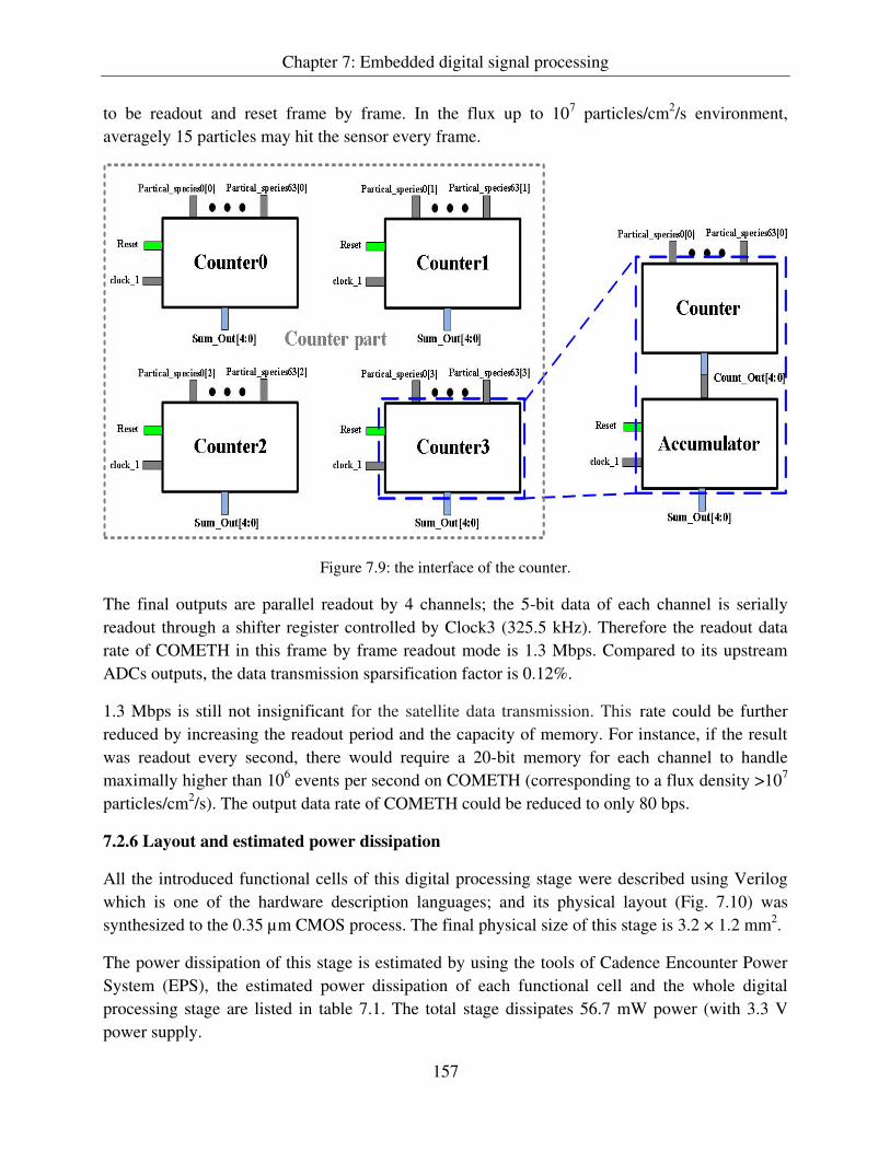
Chapter 7: Embedded digital signal processing
157
to be readout and reset frame by frame. In the flux up to 107 particles/cm
2/s environment,
averagely 15 particles may hit the sensor every frame.
Figure 7.9: the interface of the counter.
The final outputs are parallel readout by 4 channels; the 5-bit data of each channel is serially
readout through a shifter register controlled by Clock3 (325.5 kHz). Therefore the readout data
rate of COMETH in this frame by frame readout mode is 1.3 Mbps. Compared to its upstream
ADCs outputs, the data transmission sparsification factor is 0.12%.
1.3 Mbps is still not insignificant for the satellite data transmission. This rate could be further
reduced by increasing the readout period and the capacity of memory. For instance, if the result
was readout every second, there would require a 20-bit memory for each channel to handle
maximally higher than 106 events per second on COMETH (corresponding to a flux density >10
7
particles/cm2/s). The output data rate of COMETH could be reduced to only 80 bps.
7.2.6 Layout and estimated power dissipation
All the introduced functional cells of this digital processing stage were described using Verilog
which is one of the hardware description languages; and its physical layout (Fig. 7.10) was
synthesized to the 0.35 µm CMOS process. The final physical size of this stage is 3.2 × 1.2 mm2.
The power dissipation of this stage is estimated by using the tools of Cadence Encounter Power
System (EPS), the estimated power dissipation of each functional cell and the whole digital
processing stage are listed in table 7.1. The total stage dissipates 56.7 mW power (with 3.3 V
power supply.

Chapter 7: Embedded digital signal processing
158
3.2 mm
1.2
mm
Figure 7.10: Physical layout of the digital processing stage.
Table 7.1: Estimated power dissipation of each functional cell and the whole digital processing stage.
Power supply: 3.3 V Functional cell mW
Total of a single column: 0.87252 mW
Memory_temp 0.068
FSM1_N 0.03351
Adder_Column 0.09566
Adder×3 0.1445
SUM_Controller 0.4736
FSM2_N 0.05725
Total of counting and output: 0.87397 mW
The counter and final output part 0.87397
Total of the digital processing stage: 0.87252×64+0.87397 ≈ 56.7 mW
7.3 Reconstruction performances
The full simulation of the layout against many inputs has checked its performances. Results show
all the normal convex clusters could be reconstructed correctly. However in real operation,
concave clusters may also appear which are caused by unexpected un-fired pixels. Some
examples are displayed in Fig. 7.11. Each square with a centered “1” represents a fired pixel and “0” represents an un-fired pixel. The red color un-fired pixels in the examples are expected to be
fired; they are referred to as “dead” pixels in this context for a simple expression.
The reasons caused these “dead” pixels exist at the charge collection phase and each stage of
signal processing. During the charge collection phase, the amount of charges collected by a
sensing diode mainly related to its distance to the charges generated position. There are still some
fluctuations because the charge thermal diffusion inside the sensitive layer is a random process. A
“dead” pixel between two fired pixels may appear when its collected signal is a little bit lower than the ADC threshold.
The gain of the in-pixel pre-amplifier also has some fluctuations from pixel to pixel, due to the
realistic variations in the process and fluctuation of bias voltages to each pixel. If a signal closed

Chapter 7: Embedded digital signal processing
159
to the “threshold” was insufficiently amplified in the pixel, it would be determined as “0” in the
downstream ADC stage.
Beside the charge collection and pre-amplifier gain fluctuations, the FPN between ADC columns
is another reason lead to these “dead” pixels. The same pixel signal analogue value in different columns may be determined as different digital values. The methods and technologies used to
minimize the the un-uniformity of pixels and columns ADCs have been discussed in previous
chapters. This section will focus on the discussion of the reconstruct performances of the digital
processing stage for these tricky clusters caused by “dead” pixels.
These tricky clusters could be simply classified by the “dead” pixel numbers and positions. Because of their extremely small opportunities, the events of more than three adjacent “dead” pixels are not discussed.
7.3.1 Tricky cluster cases could be reconstructed correctly
Simulations results show the embedded algorithm could handle a single “dead” pixel in a cluster no matter where it is, and most of the cases for two “dead” pixels. These cases are listed below by
the “dead” pixels positions relative to the cluster.
1. “Dead” pixels in the middle of the cluster first row
All the cluster cases with “dead” pixels in the first row could be reconstructed correctly no matter these “dead” pixels are divided or adjacent.
0 0 0
0 0 0
0 1 0
0 0 0
0 0 0
1 1 0
1 1 1
0 0 1
0 0 0
1 1 0
1 1 0
0 0 0
0
1
1
0 0 0
0 0 0
0 1 0
0 0 0
0 0 0
1 1 1
1 1 1
0 0 1
0 0 0
1 1 0
1 1 0
0 0 0
1
1
0
0 0 0
0 0 0
0 0 1
0 0 0
0 0 0
1 1 0
0 0 1
0 0 1
0 0 0
1 1 0
1 1 0
0 0 0
0
1
1
Figure 7.11: Examples of “dead” pixels in the middle of the cluster first row.
2. “Dead” pixels in the middle of the cluster edge columns
All the cluster cases with “dead” pixels in the middle of the edge columns could be reconstructed
correctly no matter these “dead” pixels are divided or adjacent.
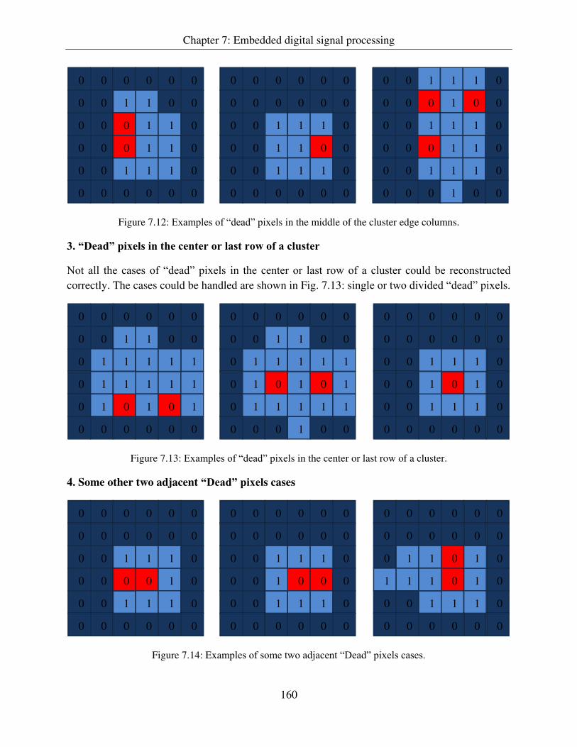
Chapter 7: Embedded digital signal processing
160
0 0 0
0 0 1
0 0 0
0 0 0
1 0 0
1 1 0
0 0 1
0 0 1
0 0 0
1 1 0
1 1 0
0 0 0
1
0
1
0 0 0
0 0 0
0 0 1
0 0 0
0 0 0
1 1 0
0 0 1
0 0 1
0 0 0
1 0 0
1 1 0
0 0 0
1
1
1
0 0 1
0 0 0
0 0 1
1 1 0
1 0 0
1 1 0
0 0 1
0 0 1
0 0 0
1 1 0
1 1 0
1 0 0
1
0
1
Figure 7.12: Examples of “dead” pixels in the middle of the cluster edge columns.
3. “Dead” pixels in the center or last row of a cluster
Not all the cases of “dead” pixels in the center or last row of a cluster could be reconstructed correctly. The cases could be handled are shown in Fig. 7.13: single or two divided “dead” pixels.
0 0 0
0 0 0
0 0 1
0 0 0
0 0 0
1 1 0
0 0 1
0 0 1
0 0 0
0 1 0
1 1 0
0 0 0
1
1
1
0 0 0
0 0 1
0 1 1
0 0 0
1 0 0
1 1 1
0 1 1
0 1 1
0 0 0
1 0 1
1 1 1
1 0 0
1
0
1
0 0 0
0 0 1
0 1 1
0 0 0
1 0 0
1 1 1
0 1 1
0 1 0
0 0 0
1 1 1
1 0 1
0 0 0
1
1
1
Figure 7.13: Examples of “dead” pixels in the center or last row of a cluster.
4. Some other two adjacent “Dead” pixels cases
0 0 0
0 0 0
0 0 1
0 0 0
0 0 0
1 1 0
0 0 1
0 0 1
0 0 0
0 1 0
1 1 0
0 0 0
1
0
1
0 0 0
0 0 0
0 1 1
0 0 0
0 0 0
1 1 0
1 1 1
0 0 1
0 0 0
0 1 0
1 1 0
0 0 0
0
1
1
0 0 0
0 0 0
0 0 1
0 0 0
0 0 0
1 1 0
0 0 1
0 0 1
0 0 0
0 0 0
1 1 0
0 0 0
1
1
1
Figure 7.14: Examples of some two adjacent “Dead” pixels cases.

Chapter 7: Embedded digital signal processing
161
For these two adjacent “dead” pixels cases, if one of the two “dead” pixels is located at the edge columns or the first row of the cluster, they could be reconstructed correctly.
7.3.2 Tricky cluster cases which lead to reconstruction failures
Reconstruction failure only occurs for some cases of two adjacent “dead” pixels, which leads to the reconstruction of single impact as several events.
1. Two adjacent “dead” pixels in the center of a cluster
0 0 0
0 0 1
0 1 1
0 0 0
1 0 0
1 1 1
0 1 1
0 1 1
0 0 0
0 1 1
1 1 1
1 0 0
1
0
11 2
3
0 0 0
0 0 1
0 1 1
0 0 0
1 1 0
1 1 1
0 1 1
0 1 1
0 0 0
0 1 1
1 1 1
1 0 0
0
1
1
1
2
Figure 7.15: Reconstruction failure examples of two adjacent “dead” pixels in the center of a cluster.
Fig. 7.15 displays two reconstruction failure examples of two adjacent “dead” pixels in the center of a cluster. The single impact of the two cases will be reconstructed as 3 and 2 events
respectively. Due to the center pixels in a large cluster always collect much more charges than the
pixels in the edge, these cases theoretically can not happen unless the column ADCs FPN is
extremely large (several LSB peak to peak value).
2. One of the two adjacent “dead” pixels in the middle of the last row of a cluster
0 0 0
0 0 1
0 1 1
0 0 0
1 0 0
1 1 1
0 1 1
0 1 1
0 0 0
1 1 1
0 0 1
0 0 0
1
1
1
12 3 4
0 0 0
0 0 1
0 1 1
0 0 0
1 0 0
1 1 1
0 1 1
0 1 1
0 0 0
1 0 1
1 0 1
0 0 0
1
1
1
12
3
Figure 7.16: Reconstruction failure examples of two adjacent “dead” pixels.
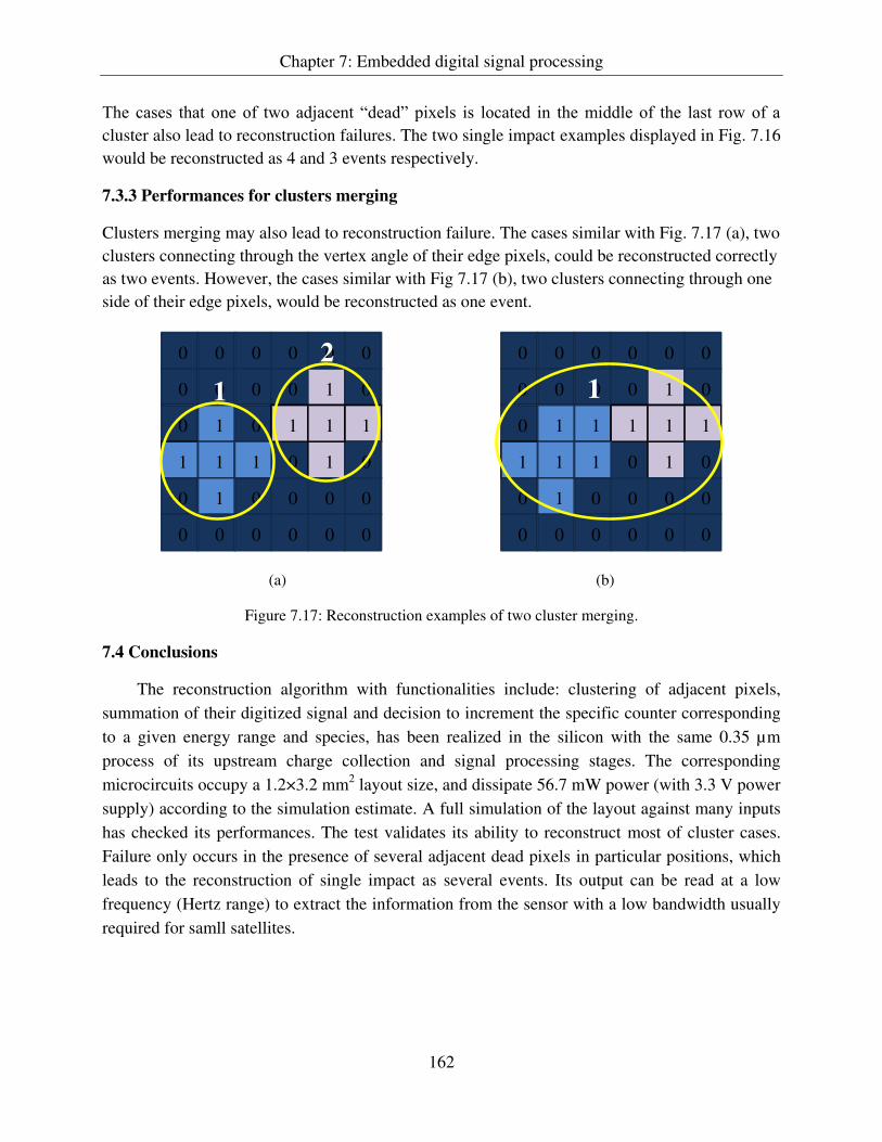
Chapter 7: Embedded digital signal processing
162
The cases that one of two adjacent “dead” pixels is located in the middle of the last row of a cluster also lead to reconstruction failures. The two single impact examples displayed in Fig. 7.16
would be reconstructed as 4 and 3 events respectively.
7.3.3 Performances for clusters merging
Clusters merging may also lead to reconstruction failure. The cases similar with Fig. 7.17 (a), two
clusters connecting through the vertex angle of their edge pixels, could be reconstructed correctly
as two events. However, the cases similar with Fig 7.17 (b), two clusters connecting through one
side of their edge pixels, would be reconstructed as one event.
0 0 0
0 0 0
0 1 1
0 0 0
0 1 0
1 1 1
1 1 1
0 1 0
0 0 0
0 1 0
0 0 0
0 0 0
1
1
1
1
0 0 0
0 0 0
0 1 0
0 0 0
0 1 0
1 1 1
1 1 1
0 1 0
0 0 0
0 1 0
0 0 0
0 0 0
1
1
1
1
2
(a) (b)
Figure 7.17: Reconstruction examples of two cluster merging.
7.4 Conclusions
The reconstruction algorithm with functionalities include: clustering of adjacent pixels,
summation of their digitized signal and decision to increment the specific counter corresponding
to a given energy range and species, has been realized in the silicon with the same 0.35 µm
process of its upstream charge collection and signal processing stages. The corresponding
microcircuits occupy a 1.2×3.2 mm2 layout size, and dissipate 56.7 mW power (with 3.3 V power
supply) according to the simulation estimate. A full simulation of the layout against many inputs
has checked its performances. The test validates its ability to reconstruct most of cluster cases.
Failure only occurs in the presence of several adjacent dead pixels in particular positions, which
leads to the reconstruction of single impact as several events. Its output can be read at a low
frequency (Hertz range) to extract the information from the sensor with a low bandwidth usually
required for samll satellites.

Chapter 7: Embedded digital signal processing
163
Bibliography
[1] F. Ananasso, F. Delli Pricoli. The Role of Satellites in Personal Communications Services. IEEE
Journal on Selected Areas in Communications. V 13, N 2, pp. 180-195, 1995.
[2] Bruce R. Elbert. The satellite communication applications handbook. 1997 Artech House, Inc,
MA.
[3] W. Shaojun, et al. Design of Data transmission speed for small high resolution satellite.
International conference on Transportation, Mechanical, and Electrical Engineering. 2011.
[4] H. Helvajian, S.W. Janson. Small Satellites: Past, Present, and Future. The Aerospace Press,
October 30, 2009
[5] Sandau, R., International study on Cost-Effective Earth Observation Missions. Taylor &
Francis, London/Leiden/New York/Philadelphia/Singapore, 2006.

164
General conclusions
The objective of this thesis is to design and develop a sensor for space ionising radiation monitor
which provides measurements of comparable or better quality than existing instruments, but at
around an order of magnitude lower power consumption, mass and volume and a lower unit cost.
According to current NASA models, the earth orbit environment is populated by a great variety
of energetic charged particles which are dominated by protons and electrons. Their total
omnidirectional fluxes may reach several 107·cm
-2·s
-1 with energies covering many orders of
magnitude (for protons in the range 0.1 - 400 MeV and electrons in the range 0.04 - 7 MeV).
We proposed a new strategy to cope with this high flux mixed particles environment with a single
CMOS pixel chip, which is a highly integrated detection system with the ability to count and
identify ion species in real-time.
The sensor responses to various particles energies and species were simulated using the response
model we build from the results of the state-of-the-art CPS developed by the CMOS research
group at IPHC. Simulations indicate the possibility to evaluate the dose deposited by an ionizing
radiation in a large energy range (100 keV to few 100 MeV) and to distinguish protons from
electrons using their linear energy transfer below an energy of 50 MeV.
A CPS architecture named COMETH was proposed and designed in a 0.35 µm process. It
features a sensitive area of about 10 mm2 which is a 64×64 square pixel matrix with 50 µm pitch
size, while the total area comprising the data treatment micro-circuits reaches about 17 mm2.
COMETH is designed to operate in the rolling-shutter mode reaching a 65,000 frames/s read-out
speed; and its total estimated power dissipation is about 100 mW (under 3.3 V power supply).
A single 4.3×4.3 µm2 n-well/p-epi sensing diode located in the center of each pixel collects the
charges generated in the sensitive layer of the sensor. Still within the pixel, the sensing diode
signal goes through a pre-amplification stage and undergoes a Correlated Double Sampling
(CDS). Then, outside the sensitive area, column-level ADCs digitize over 3 bits the signals of an
entire row. The final digital processing occurs in an embedded algorithm integrated on the chip. It
consists in the embedded algorithm, which processes the ADCs digital outputs. Its functionalities
include: clustering of adjacent pixels, summation of their digitized signal and decision to

General conclusions
165
increment the specific counter corresponding to a given energy range and species. Indeed, a
memory containing several counters, one per energy and species, forms the final result of the
sensor. This memory can then be read at a low frequency (Hertz range) to extract the information
from the sensor with a low bandwidth usually required for small satellites.
The previous features result from an optimization conducted with simulated data to guarantee
robust flux estimation by species up to 107 particles•cm-2•s-1
. In particular, the sensor response
model used, predicted individual pixel charges from a hundred e- to 4400 e
-; electron cluster size
between 2 to 3 pixels; and low energy protons firing sub-area as large as 9×9 pixels with the
cluster size being inversely proportional to the incident energy. The design of the three main
signal processing stages was driven by these expectations.
A reduced scale prototype with 32×32 pixels and 32 column ADCs was fabricated and tested to
validate the COMETH concept. The pixel matrix was illuminated with three types of radiations:
monochromatic X-rays to obtain the charge to voltage conversion factor (CVF) and the charge
collection efficiency (CCE); Beta electrons to assess the sensitivity to minimum ionizing particles
with the signal over noise ratio (SNR) and the cluster shape; and finally infrared photons from a
focalized laser beam to test the pixel response linearity over the relevant signal range and the
sensing diode reset and recovery efficiency. The end-column ADCs were tested with external
biased voltage replacing the pixel outputs. Their noise performances, transfer function, power
dissipation and tunable threshold functionality have been measured.
Tests of the pixel matrix corroborate the expectation from previous simulations on the key
parameters: charge collection efficiency, detection efficiency for minimum ionizing particles,
cluster size of a few pixels, and linearity over the expected signal range. Separate evaluation of
the analogue to digital conversion stage over 3 bits was also satisfactory. The embedded digital
processing algorithm, which achieves the final flux evaluation online, was also synthesized and
validated.
All these elements make us confident that a CMOS radiation counter with very low mass and
power can indeed measure high flux up to the 107 particles·cm
-2·s
-1 flux, as our previous
simulation work indicated.
The steps needed before the possible production of the complete monitor include: measurement
of the prototype sensor response to low energy protons; reduction of the pixel noise and of the
ADC FPN between columns, and further optimization of the system power dissipation.

166
Appendix A
Test board schematic for the prototype of
COMETH

Appendix A : Test board schematic for the prototype of COMETH
167
13
LV
DS
Dig
ita
l O
utp
uts
& 6
co
ntr
ol
sig
na
ls
16
An
alo
gu
e b
ias
& 8
An
alo
gu
e O
utp
uts
& c
hip
po
we
rs
02
/20
13
CO
ME
TH
_p
cb
Ya
ng
ZH
OU
/KK
J
Ya
ng
ZH
OU
/KK
J
CO
ME
TH
pro
xim
ity
bo
ard
24
Dig
ita
l L
VD
S I
np
uts
SM
C C
AB
LE
: 1
ST
WIR
E P
IN B
1,
LA
ST
WIR
E A
25
SM
C C
ON
NE
CT
OR
: P
IN B
1 I
S I
N R
ED
MA
RK
ED
LA
ST
_M
OD
IFIE
D=
Fri
Ap
r 0
5 0
9:0
1:4
8 2
01
3
1/5
D:\
pro
jets
\CA
O\C
OM
ET
H_
PC
B\C
OM
ET
H_
PR
OX
_P
CB
\co
me
th_
pro
x_p
cb.c
pm
TIT
LE
=co
me
th_
pro
x
1u
1u
ST
AN
6V
47
u
10
u
1/1 --XFAB 035--C
HIP
47
u
10
0n
10
0n
10
0n
10
0n
10
u
CO
ME
TH
1u
SM
C-Q
-V-6
.7
SM
C-Q
-V-6
.7
47
u4
7u
10
0n
1u
1u
10
u
47
u
SM
C-Q
-V-6
.7
SM
C-Q
-V-6
.7
(GN
D)
10
0n
10
0n
10
0n
1u
C1
2
C8
C5
2
C4
9
C2
J7
J5
J6
J8
L3
C8
3C
77
L2
C8
2C
85
C8
8C
91
C9
4C
76
C9
3C
90
C8
7C
84
L1
C8
1C
75
IC1
CP
RE
SU
LT
_P
CP
RE
SU
LT
_N
SO
SH
IFT
_P
SO
RE
SE
T_
N
VD
DA
_T
ES
T
DB
0_
N
DO
4_
P
VD
DA
_IN
GN
D\G
CP
_R
ES
UL
TS
S4
AO
2
GN
D\G
GN
D\G
PIX
ST
_N
GN
D\G
VD
D_
BU
F
V_
BU
FF
ER
GN
D\G
CL
EA
R
PIX
EL
_C
LK
GN
D\G
GN
D\G
AB
UF
_N
GN
D\G
AB
UF
_N
GN
D\G
AB
UF
_N
GN
D\G
AI_
LV
DS
BIA
SA
I_R
EF
AM
PA
I_F
CA
I_R
ES
ET
_D
IOD
EA
I_T
ES
T1
AI_
TE
ST
2G
ND
\GA
I_V
CM
PIX
AI_
VD
RA
I_V
R1
AI_
VR
2G
ND
\GV
DD
_IN
GN
D\G
VD
DA
_IN
AB
UF
_P
A7
A6
A5
A4
A1
A2
A0
PIS
O_
SH
IFT
GN
D\G
PIX
ST
_P
DB
4_
N
DB
2_
P
GN
D\G
DB
6_
PG
ND
\G
DO
7_
PD
O7
_N
DO
6_
PD
O6
_N
DO
5_
PD
O5
_N
DO
4_
N
OF
FS
ET
_C
AN
CE
L
CL
K_
LA
TC
H
SL
EE
PC
LK
AD
C
PO
WE
RO
NN
+1
PO
WE
RO
NN
RS
TA
DC
PIS
O_
CL
K
GN
D\G
S_
SH
BU
FF
ER
_IN
GN
D\G
VR
1
AO
0
GN
D\G
DB
6_
NR
ES
_1
FIN
I_N
RE
SE
T2
RE
SE
T1
PIX
EL
_S
TA
RT
DB
5_
N
DB
3_
P
PIX
CL
K_
P
2P
IXC
LK
_P
S1
_N
S2
_P
VD
D_
BU
F
GN
D\G
VD
D_
BU
F
GN
D\G
VC
M_
PIX
GN
D\G
DB
5_
PG
ND
\G
AO
1
GN
D\G
GN
D\G
DB
1_
N
R0
_P
RD
_N
GN
D\G
DB
4_
PG
ND
\G
GN
D\G
DB
2_
N
DB
7_
PG
ND
\G
GN
D\G
R2
_N
SH
1S
ET
GN
D\G
GN
D\G
RS
T2
_P
GN
D\G
PIX
CL
K_
NG
ND
\G
SO
CL
K_
P
GN
D\G
SH
1_
PG
ND
\G
GN
D\G
GN
D\G
SO
RE
SE
T_
PG
ND
\G
SH
1_
N
SO
CL
K_
N
SO
SH
IFT
_N
GN
D\G
GN
D\G
RS
TA
DC
_N
GN
D\G
GN
D\G
GN
D\G
SE
T_
P
GN
D\G
GN
D\G
LA
TC
HC
LK
_N
GN
D\G
OF
FS
ET
CA
NC
EL
_P
CL
KA
DC
_N
SF
C_
P
SH
2_
N
GN
D\G
GN
D\G
GN
D\G
GN
D\G
GN
D\G
GN
D\G
RS
TA
DC
_P
VD
DA
2P
IXE
L_
CL
K
VD
DA
_T
ES
T_
IN
S1
I_B
IAS
_IN
V_
RE
SE
T_
DIO
DE
V_
TE
ST
2
I_A
DR
IVE
RI_
SF
BIA
S
PIS
O_
RE
SE
T
AO
7
S_
UN
LV
DS
AO
3A
O4
AO
5A
O6
S2
S3
SH
2
DO
3_
P
VD
DA
S_
FC
EN
_T
VD
D_
IN
DIS
AD
C
SE
L
VR
2
VD
R
LV
DS
_V
CM
GN
D\G
GN
D\G
GN
D\G
VR
EF
_A
MP
V_
TE
ST
1
V_
CL
P
GN
D\G
VD
D
LA
TC
HC
LK
_P
GN
D\G
DO
3_
N
S2
_N
RS
T1
_N
GN
D\G
CL
R_
NG
ND
\G
PO
N_
P
PO
N+
1_
N
GN
D\G
S4
_P
S3
_N
GN
D\G
S1
_P
RS
T1
_P
CL
R_
PG
ND
\G2
PIX
CL
K_
NG
ND
\G
GN
D\G
GN
D\G
VD
D_
BU
F
VD
D_
BU
F
RS
T2
_N
PO
N_
N
PO
N+
1_
P
VD
D_
BU
F
GN
D\G
VD
D_
BU
F
DB
1_
P
V_
FC
FIN
I_P
R1
_N
DIS
AD
C_
INS
LE
EP
_IN
SE
L_
INS
_U
NL
VD
S_
IN
SE
T_
N
SH
2_
PG
ND
\G
GN
D\G
AB
UF
_P
GN
D\G
VB
AS
E
A3
VD
D_
BU
FS
3_
P
R2
_P
DB
7_
N
DB
3_
N
DB
0_
P
EN
_T
_IN
R1
_P
R0
_N
RD
_P
DO
1_
P
DO
2_
ND
O2
_P
VD
D
FR
AM
E_
FIN
I
RE
S_
DR
ES
_0
RE
S_
2
DO
0_
ND
O0
_P
DO
1_
N
AI_
BU
FF
ER
GN
D\G
AI_
CL
P
VD
DA
_T
ES
T_
IN
AI_
SF
BIA
SA
I_L
VD
SV
CM
AI_
AD
RIV
ER
AI_
BIA
S_
IN
VD
D_
INV
DD
_IN
VD
DA
_IN
VD
DA
_IN
GN
D\G
CL
KA
DC
_P
GN
D\G
AB
UF
_P
GN
D\G
S_
SH
BU
FF
ER
I_L
VD
S_
BIA
S
S4
_N
OF
FS
ET
CA
NC
EL
_N
SF
C_
N
VD
DA
_T
ES
T
B2
5B
24
B2
3B
22
B2
1B
20
B1
9B
18
B1
7B
16
B1
5B
14
B1
3B
12
B1
1B
10
B9
B8
B7
B6
B5
B4
B3
B2
B1
A2
5A
24
A2
3A
22
A2
1A
20
A1
9A
18
A1
7A
16
A1
5A
14
A1
3A
12
A1
1A
10
A9
A8
A7
A6
A5
A4
A3
A2
A1
B2
5B
24
B2
3B
22
B2
1B
20
B1
9B
18
B1
7B
16
B1
5B
14
B1
3B
12
B1
1B
10
B9
B8
B7
B6
B5
B4
B3
B2
B1
A2
5A
24
A2
3A
22
A2
1A
20
A1
9A
18
A1
7A
16
A1
5A
14
A1
3A
12
A1
1A
10
A9
A8
A7
A6
A5
A4
A3
A2
A1
B2
5B
24
B2
3B
22
B2
1B
20
B1
9B
18
B1
7B
16
B1
5B
14
B1
3B
12
B1
1B
10
B9
B8
B7
B6
B5
B4
B3
B2
B1
A2
5A
24
A2
3A
22
A2
1A
20
A1
9A
18
A1
7A
16
A1
5A
14
A1
3A
12
A1
1A
10
A9
A8
A7
A6
A5
A4
A3
A2
A1
B2
5B
24
B2
3B
22
B2
1B
20
B1
9B
18
B1
7B
16
B1
5B
14
B1
3B
12
B1
1B
10
B9
B8
B7
B6
B5
B4
B3
B2
B1
A2
5A
24
A2
3A
22
A2
1A
20
A1
9A
18
A1
7A
16
A1
5A
14
A1
3A
12
A1
1A
10
A9
A8
A7
A6
A5
A4
A3
A2
A1
10
3
10
299
10
170
79
33
50
54
57
58
59
60
61
62
63
10
41
05
3 14
24
41
47
81
93
11
21
20
97
95
96
53
10
051
98
S
11
4 37
36
35
83
23
39
38
43
42
44
45
11
5
25
28
27
26
92
90
84
85
86
91
11
81
19
11
7
11
030
21
19
17
15
11
9 7 522
20
18
16
12
10
8 6
67
31
68
4
46
10
9
11
6
11
3
10
889
32
71
72
73
74
75
76
77
78
88
A1
3B
13
A1
B1
A2
B2
A3
B3
A4
B4
A5
B5
A6
B6
A7
B7
A8
B8
A9
B9
A1
0B
10
A1
1B
11
A1
2B
12
A1
4B
14
A1
5B
15
A1
6B
16
A1
7B
17
A1
8B
18
A1
9B
19
A2
0B
20
A2
1B
21
A2
2B
22
A2
3B
23
A2
4B
24
A2
5B
25
VD
DA
_T
ES
T
VD
DV
DD
A
V_
RE
SE
T_
DIO
DE
LV
DS
_7
LV
DS
_V
CM
VR
EF
_A
MP
FR
AM
E_
FIN
I
RE
SU
LT
_D
RE
SU
LT
_0
RE
SU
LT
_1
RE
SU
LT
_2
LV
DS
_0
LV
DS
_3
LV
DS
_2
LV
DS
_1
LV
DS
_6
LV
DS
_5
LV
DS
_4
CL
KA
DC
SL
EE
PD
ISA
DC
RS
TA
DC
CL
K_
LA
TC
HC
P_
RE
SU
LT
SO
FF
SE
T_
CA
NC
EL
S1
S2
S3
S4
SE
TS
H1
SH
2
S_
FC
PIS
O_
CL
KP
ISO
_R
ES
ET
PIS
O_
BW
RIT
E_
SH
IFT
EN
_T
S_
SH
BU
FF
ER
S_
UN
LV
DS
SE
L
SU
BS
V_
FC
V_
CL
P
VC
M_
PIX
VD
RV
R1
V_
TE
ST
1
AN
AO
UT
<1
>
AN
AO
UT
<3
>
AN
AO
UT
<6
>V
_B
UF
FE
R
V_
TE
ST
2
BIA
S_
IN
VR
2
AN
AO
UT
<0
>
AN
AO
UT
<2
>
AN
AO
UT
<4
>A
NA
OU
T<
5>
AN
AO
UT
<7
>
PO
WE
RO
NN
+1
PO
WE
RO
NN
PIX
EL
_S
TA
RT
RE
SE
T2
RE
SE
T1
CL
EA
R
PIX
EL
_C
LK
I_S
FB
IAS
I_A
DR
IVE
R
2P
IXE
L_
CL
K
I_L
VD
S_
BIA
S
+ +GN
D
GN
D
++
A2
A1
A3
A4
A5
A6
A8
A9
A1
0
A1
1
A1
2
A1
3
A1
4
A1
5
A1
6
A1
7
A1
8
A1
9
A2
0
A2
1
A2
2
A2
3
A2
5
A2
4
B1
B2
B6
B5
B4
B3
B1
2
B1
1
B1
0
B9
B8
B1
7
B1
6
B1
5
B1
4
B1
3
B2
2
B2
1
B2
0
B1
9
B1
8
B2
3
B2
4
B2
5
B7
A7
A1
3B
13
A1
B1
A2
B2
A3
B3
A4
B4
A5
B5
A6
B6
A7
B7
A8
B8
A9
B9
A1
0B
10
A1
1B
11
A1
2B
12
A1
4B
14
A1
5B
15
A1
6B
16
A1
7B
17
A1
8B
18
A1
9B
19
A2
0B
20
A2
1B
21
A2
2B
22
A2
3B
23
A2
4B
24
A2
5B
25
A1
3B
13
A1
B1
A2
B2
A3
B3
A4
B4
A5
B5
A6
B6
A7
B7
A8
B8
A9
B9
A1
0B
10
A1
1B
11
A1
2B
12
A1
4B
14
A1
5B
15
A1
6B
16
A1
7B
17
A1
8B
18
A1
9B
19
A2
0B
20
A2
1B
21
A2
2B
22
A2
3B
23
A2
4B
24
A2
5B
25
GN
D
+GN
D
EE
PA
GE
:
RE
F:
DA
TE
:D
ES
SIN
:
ET
UD
E:
AA
BCC
D
1
2 233
4 455
6 677
8 8
D
1
B
TIT
RE
ST
RA
SB
OU
RG
HU
BE
RT
CU
RIE
N
INS
TIT
UT
PLU
RID
ISC
IPLI
NA
IRE
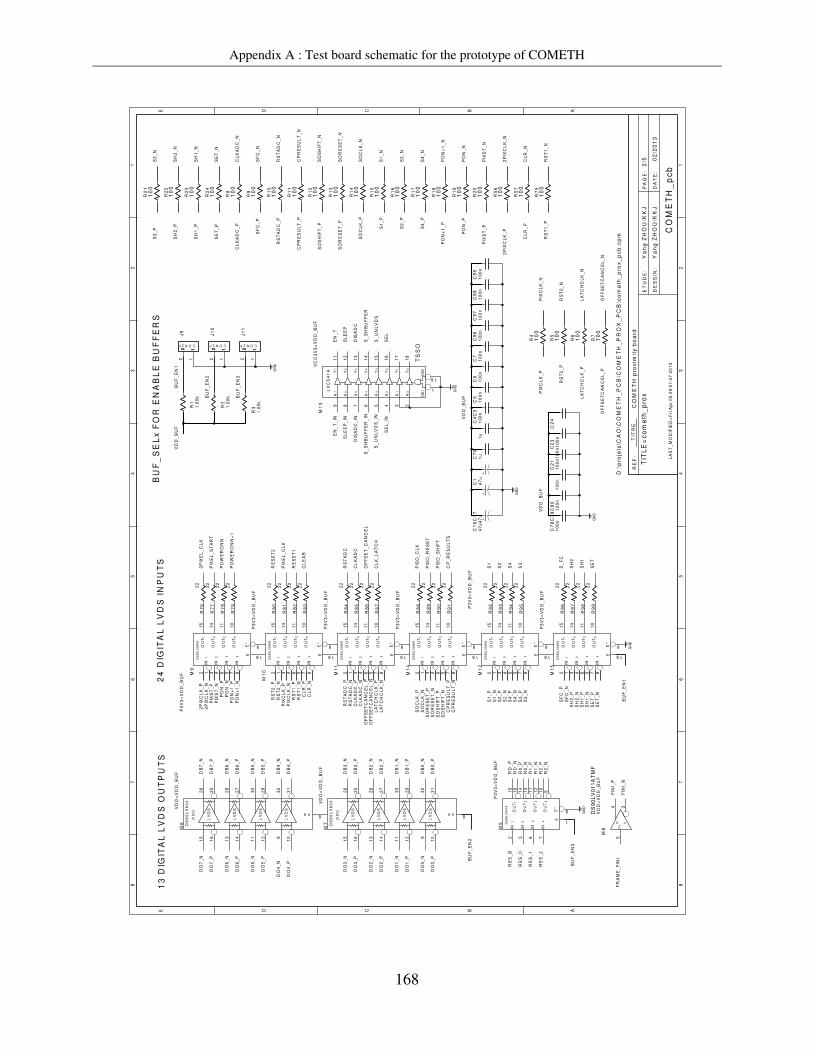
Appendix A : Test board schematic for the prototype of COMETH
168
24
DIG
ITA
L L
VD
S I
NP
UT
S
13
DIG
ITA
L L
VD
S O
UT
PU
TS
CO
ME
TH
pro
xim
ity
bo
ard
BU
F_
SE
Lx
FO
R E
NA
BL
E B
UF
FE
RS
Ya
ng
ZH
OU
/KK
J
Ya
ng
ZH
OU
/KK
J
CO
ME
TH
_p
cb
02
/20
13
TIT
LE
=co
me
th_
pro
x
LA
ST
_M
OD
IFIE
D=
Fri
Ap
r 0
5 0
9:0
1:4
7 2
01
3
2/5
D:\
pro
jets
\CA
O\C
OM
ET
H_
PC
B\C
OM
ET
H_
PR
OX
_P
CB
\co
me
th_
pro
x_p
cb.c
pm
12 12 12
VD
D=
VD
D_
BU
F1
00
10
0
10
0
10
0
10
0
10
0
1.0
0k
1.0
0k
10
0
(VD
D)
10
0
DS
90
LV
80
4
(VD
D)
10
0
10
0
10
0
10
0
10
0
10
0
10
0
10
0
10
0
10
0
10
0
10
0
10
0
10
0
10
0
VD
D=
VD
D_
BU
F
1.0
0k
TS
SO
VC
C3
V3
=V
DD
_B
UF
P3
V3
=V
DD
_B
UF
DS
90
LV
80
4
VD
D=
VD
D_
BU
FD
S9
0L
V0
11
AT
MF
10
0
10
0n
10
0n
10
0n
10
0n
10
0n
10
0n
10
0n
1u
1u
47
u
P3
V3
=V
DD
_B
UF
47
u4
7u
22
22
22
22
22
22
22
22
22
22
22
22
22
22
22
22
22
22
22
22
22
22
22
22
P3
V3
=V
DD
_B
UF
P3
V3
=V
DD
_B
UF
P3
V3
=V
DD
_B
UF
P3
V3
=V
DD
_B
UF
10
0n
10
0n
10
0n
10
0n
10
0n
10
0n
10
0n
P3
V3
=V
DD
_B
UF
C2
4C
23
C2
1
C1
6C
17
C7
8C
79
C8
0
C9
9C
98
C9
7C
96
M1
3
R9
8
R9
9
R9
7
R9
6
R9
5
R9
3
R9
4
R9
2
R9
1
R9
0
R8
9
R8
8
R8
6
R8
7
R8
4
R8
5
R8
3
R8
2
R8
1
R8
0
R7
6
R7
7
R7
8
R7
9
C7
0
R7
R6
R5
R4
R7
5
R5
7
R5
6
R2
0
R1
9
R1
8
R1
7
R1
6
R1
2
R1
3
R1
4
R1
5
R8
R9
R1
0
R1
1
R3
J1
1
R2
J1
0
R1
J9
M1
5
M1
2C
7C
6C
5C
4C
3C
1
M8M
5
R2
4
R2
3
R2
2
R2
1
M1
4
M1
1
M1
0M9
M7
M6
OF
FS
ET
CA
NC
EL
_P
DO
4_
P
BU
F_
EN
2
DB
2_
N
OF
FS
ET
CA
NC
EL
_P
EN
_T
_IN
EN
_T
DIS
AD
C
S_
SH
BU
FF
ER
SE
L
S_
UN
LV
DS
SL
EE
P_
IN
DIS
AD
C_
INS
OC
LK
_P
CP
RE
SU
LT
_N
SE
T_
N
BU
F_
EN
3
OF
FS
ET
CA
NC
EL
_N
DB
4_
P
SO
RE
SE
T_
N
SO
SH
IFT
_P
SO
CL
K_
N
SO
RE
SE
T_
P
S1
_N
S2
_N
S3
_P
SH
1_
N
DB
0_
P
DB
0_
N
DB
1_
P
DB
1_
N
DB
2_
P
DB
3_
N
DB
4_
N
DB
5_
N
DB
6_
N
DB
7_
P
DO
0_
P
DO
0_
N
DO
1_
P
DO
1_
N
DO
2_
P
DO
3_
N
DO
4_
N
DO
5_
P
DO
5_
N
DO
6_
N
DO
6_
P
DO
7_
N
DO
7_
P
SF
C_
P
PO
N+
1_
P
SF
C_
N
CL
KA
DC
_P
RS
TA
DC
_P
BU
F_
EN
1
BU
F_
EN
2
RS
T1
_P
RD
_N
RD
_P
R0
_N
R1
_P
RE
S_
D
BU
F_
EN
3
S2
_P
SH
1_
P
SH
2_
N
RS
TA
DC
_N
SE
T_
P
RS
T1
_N
LA
TC
HC
LK
_N
S3
_N
CP
RE
SU
LT
_P
SO
SH
IFT
_N
S1
_P
S4
_P
S4
_N
PO
N+
1_
N
PO
N_
PP
ON
_N
PIX
ST
_P
PIX
ST
_N
2P
IXC
LK
_N
CL
R_
PC
LR
_N
2P
IXC
LK
_P
RS
T2
_N
PIX
CL
K_
N
SH
2_
P
DB
6_
P
DB
3_
P
LA
TC
HC
LK
_P
VD
D_
BU
F
DB
7_
N
S_
SH
BU
FF
ER
_IN
S_
UN
LV
DS
_IN
SE
L_
IN
RE
S_
0R
0_
P
R1
_N
RE
S_
1
FIN
I_N
DO
3_
P
DO
2_
N
FR
AM
E_
FIN
I
R2
_P
R2
_N
FIN
I_P
RE
S_
2
VD
D_
BU
F
SE
T_
P
BU
F_
EN
1
PO
N+
1_
PP
ON
+1
_N
PO
N_
NP
ON
_P
PIX
ST
_N
PIX
ST
_P
2P
IXC
LK
_N
2P
IXC
LK
_P
CL
R_
PC
LR
_N
RS
T1
_N
RS
T1
_P
PIX
CL
K_
NP
IXC
LK
_P
RS
T2
_N
RS
T2
_P
LA
TC
HC
LK
_P
LA
TC
HC
LK
_N
OF
FS
ET
CA
NC
EL
_N
CL
KA
DC
_N
CL
KA
DC
_P
RS
TA
DC
_N
RS
TA
DC
_P
CP
RE
SU
LT
_P
CP
RE
SU
LT
_N
SO
SH
IFT
_N
SO
SH
IFT
_P
SO
RE
SE
T_
NS
OR
ES
ET
_P
SO
CL
K_
NS
OC
LK
_P
S3
_P
S3
_N
S4
_N
S4
_P
S2
_N
S2
_P
S1
_N
S1
_P
SE
T_
N
SH
1_
NS
H1
_P
SH
2_
NS
H2
_P
SF
C_
NS
FC
_P
CL
KA
DC
_N
RS
T2
_P
2P
IXE
L_
CL
K
PIX
EL
_S
TA
RT
PO
WE
RO
NN
+1
RE
SE
T2
RE
SE
T1
PIX
EL
_C
LK
CL
EA
R
RS
TA
DC
CL
K_
LA
TC
H
OF
FS
ET
_C
AN
CE
L
PIS
O_
CL
K
PIS
O_
RE
SE
T
PIS
O_
SH
IFT
CP
_R
ES
UL
TS
S1
S2
S4
S_
FC
SH
2
SH
1
SE
T
PO
WE
RO
NN
SL
EE
P
DB
5_
P
CL
KA
DC
PIX
CL
K_
P
S3
VD
D_
BU
F
11
12
13
14
15
16
17
18
19
1
9 8 7 6 5 4 3 2
2 12 12 1
10
11
14
15
87564312
9
16
10
11
14
15
87564312
9
16
345
8
1
910
12
11
13
14
16
15
7632
10
11
14
15
87564312
9
16
10
11
14
15
87564312
9
16
10
11
14
15
87564312
9
16
10
11
14
15
87564312
9
16
25
27
29
31
26
28
30
32
16
14
12
10
15
13
11 9
8
25
27
29
31
26
28
30
32
16
14
12
10
15
13
11 9
8
** ****** * * *
****
****
1DS
90LV
048A
4321
33
IN ININ
2
IN
OU
T
OU
T
OU
T
OU
T
E*
E
***** * * ** *
1DS
90LV
048A
4321
33
IN ININ
2
IN
OU
T
OU
T
OU
T
OU
T
E*
E
* *
*
GN
D
CON2P
2 1
*
CON2P
2 1
*
LV
DS
LV
DS
LV
DS
LV
DS
EN
CON2P
2 1
GN
D
1DS
90LV
048A
4321
33
IN ININ
2
IN
OU
T
OU
T
OU
T
OU
T
E*
E
1DS
90LV
048A
4321
33
IN ININ
2
IN
OU
T
OU
T
OU
T
OU
T
E*
E
LV
DS
LV
DS
LV
DS
LV
DS
EN
+
GN
D
O+
O-
TT
L
GN
D
INO
UT
OU
T
OU
T
OU
TIN
2
E*
E
IN
DS
90LV
047A
IN
1 2 3 4
1 3 4
****
1DS
90LV
048A
4321
33
IN ININ
2
IN
OU
T
OU
T
OU
T
OU
T
E*
E
+
+
GN
D
GN
D
A OE10
AAA3 2 1
AA5 4
AA
67LV
C5
41
A Y0
OE2Y YY
2 13
Y Y
5 4
Y Y
7 6
* **
1DS
90LV
048A
4321
33
IN ININ
2
IN
OU
T
OU
T
OU
T
OU
T
E*
E
*** *******
EE
PA
GE
:
RE
F:
DA
TE
:D
ES
SIN
:
ET
UD
E:
AA
BCC
D
1
2 233
4 455
6 677
8 8
D
1
B
TIT
RE

Appendix A : Test board schematic for the prototype of COMETH
169
Ya
ng
ZH
OU
/KK
J
Ya
ng
ZH
OU
/KK
J
CO
ME
TH
_p
cb
02
/20
13
CO
ME
TH
pro
xim
ity
bo
ard
An
alo
gu
e O
utp
ut
sig
na
ls s
ing
le-e
nd
ed
bu
ffe
rs LA
ST
_M
OD
IFIE
D=
Fri
Ap
r 0
5 0
9:0
1:4
7 2
01
3
D:\
pro
jets
\CA
O\C
OM
ET
H_
PC
B\C
OM
ET
H_
PR
OX
_P
CB
\co
me
th_
pro
x_p
cb.c
pm
3/5
TIT
LE
=co
me
th_
pro
x
LMH
6628
10
0n
51
11
.21
k
LMH
6628
LMH
6628
49
.9
51
11
.21
k
49
.9
LMH
6628
47
u4
7u
47
u4
7u
10
0n
10
0n
10
0n
10
0n
10
0n
10
0n
10
0n
10
0n
47
u4
7u
0000
000
0
10
0n
10
0n
10
0n
10
0n
51
11
.21
k4
9.9
51
11
.21
k
LMH
6628
49
.9
LMH
6628
49
.9
51
11
.21
k
LMH
6628
49
.9
51
11
.21
k4
9.9
51
1
51
1
1.2
1k
LMH
6628
49
.9
06
03
-1%
1.2
1k
C3
0C
31
C3
6C
37
C1
8C
19
C1
4C
15
M1 M
4
M3
M2
M4
M3
M1
M2
C1
1C
9C
33
C3
5
R4
9R5
0
R4
3R4
4
R4
8
C3
4
R4
6R4
7
R5
2R
58
R5
4
R5
1R
55
R4
1R4
2
R4
5R
53
C1
3
R3
3R
36
R4
0
C1
0
R2
7R2
8
R3
4
R3
2R
38
R3
1
R3
0R
35
C2
5C
20
R2
9R
25R2
6
C2
2C
28
R3
9
R3
7
VB
AS
EV
BA
SE
A7
AA
A7
A2
AO
7
AA
7
AA
A4
AB
UF
_N
AB
UF
_P
AA
A6
AA
A5
AA
4
AA
A3
AB
UF
_N
AB
UF
_P
AA
3
AA
A2
AB
UF
_N
AB
UF
_P
AA
2
AA
A1
AB
UF
_N
AA
1
AA
A0
AA
0
AB
UF
_N
AB
UF
_N
AB
UF
_P
AB
UF
_N
AB
UF
_P
AB
UF
_P
AB
UF
_P
AB
UF
_N
AB
UF
_P
AB
UF
_P
AB
UF
_N
AB
UF
_P
AB
UF
_N
VB
AS
E
A6
AO
6
VB
AS
E
A5
A4
VB
AS
E
AO
5
AO
4
VB
AS
E
AO
3
A3
VB
AS
E
AO
2
VB
AS
E
AO
1
A1
A0
VB
AS
E
VB
AS
E
AO
0
AA
6
AA
5
8
31
4
2
8
57
4
6
8
57
4
6
8
31
4
2
8
31
4
2
8
31
4
2
8
57
4
6
8
57
4
6
GN
D
*
V-V+
+ -
O
GN
D
+
GN
D
+
+
+ GN
D
GN
D
+
+
**
*
**
*
V-V+
+ -
O
**
*
V-V+
+ -
O
*
*
*
V-V+
+ -
O
*
**
*
V-V+
+ -
O
*
**
V-V+
+ -
O
*
GN
D
**
*
*
V-V+
+ -
O
*
* **
***
V-V+
+ -
O
TIT
RE
EE
PA
GE
:
RE
F:
DA
TE
:D
ES
SIN
:
ET
UD
E:
AA
BCC
D
1
2 233
4 455
6 677
8 8
D
1
B

Appendix A : Test board schematic for the prototype of COMETH
170
Figure A.1: Schematic of the proximate test board of the prototype of COMETH.
4 c
urr
en
t b
ias
inp
uts
CO
ME
TH
pro
xim
ity
bo
ard
Ya
ng
ZH
OU
/KK
J
12
vo
ltag
e b
ias
inp
uts
02
/20
13
CO
ME
TH
_p
cb
Ya
ng
ZH
OU
/KK
J
LA
ST
_M
OD
IFIE
D=
Fri
Ap
r 0
5 0
9:0
1:4
7 2
01
3
4/5
D:\
pro
jets
\CA
O\C
OM
ET
H_
PC
B\C
OM
ET
H_
PR
OX
_P
CB
\co
me
th_
pro
x_p
cb.c
pm
12 12 12 12
TIT
LE
=co
me
th_
pro
x
10
k
10
k
10
k
10
k
10
k
10
k
10
k
10
k
10
k
10
k
10
k
10
k
04
02
04
02
04
02
04
02
04
02
04
02
04
02
04
02
04
02
04
02
04
02
010
0n
10
0n
10
0n
10
0n
10
0n
10
0n
10
0n
00
10
0n
10
0n
10
0n
10
0n
10
0n
10
0n
04
02
10
0n
10
0n
10
0n
10
0n
10
0n
10
0n
10
0n
10
0n
10
0n
10
0n
10
0n
10
0n
10
0n
10
0n
10
0n
0 R7
4
C7
4
J4
R7
3
C7
3
J3
R7
2 C7
2
J2J1
C7
1
R7
1
C6
9
R7
0
C6
5
R6
9
C6
4
C6
8
C6
7
R6
8
C6
6C
63
R6
7
C5
3
R6
6
C5
1
C6
2
C6
1
R6
5
C5
4
C5
0
R6
4
C4
8
R6
3
C6
0
C5
9
C4
7
R6
2
C5
8
C4
6
R6
1
C5
7
C4
5
R6
0
C5
6
R5
9
C5
5C
44
AI_
BU
FF
ER
AI_
AD
RIV
ER
AI_
FC
I_B
IAS
_IN
AI_
BIA
S_
IN
AI_
SF
BIA
S
AI_
LV
DS
BIA
S
AI_
VD
R
AI_
CL
P
AI_
LV
DS
VC
M
AI_
RE
FA
MP
AI_
VR
1
AI_
VC
MP
IXA
I_V
R2
AI_
TE
ST
2
VR
2
VR
EF
_A
MP
LV
DS
_V
CM
VR
1
VC
M_
PIX
V_
TE
ST
2
V_
TE
ST
1
V_
RE
SE
T_
DIO
DE
V_
FC
V_
BU
FF
ER
AI_
TE
ST
1
VD
R
I_L
VD
S_
BIA
S
I_A
DR
IVE
R
I_S
FB
IAS
V_
CL
P
AI_
RE
SE
T_
DIO
DE
2 12 12 12 1
GN
D
GN
D
*
CON2P
2 1
*
GN
D
*
CON2P
2 1
*
CON2P
2 1
GN
D
CON2P
2 1
GN
D
*
GN
D
*
GN
D
*
GN
D
GN
D
GN
D
GN
D
*
GN
DG
ND
*
GN
D
*
GN
D
GN
D
GN
D
GN
D
*
GN
D
GN
D
*
GN
D
**
GN
D
GN
D
GN
DG
ND
*
GN
DG
ND
*
GN
D
EE
PA
GE
:
RE
F:
DA
TE
:D
ES
SIN
:
ET
UD
E:
AA
BCC
D
1
2 233
4 455
6 677
8 8
D
1
B
TIT
RE

Appendix A : Test board schematic for the prototype of COMETH
171
CO
ME
TH
AU
X B
OA
RD
CO
ME
TH
PR
OX
BO
AR
D I
NT
ER
FA
CE
13
LV
DS
DIG
ITA
L O
UT
PU
TS
, 6
CO
NT
RO
L S
IGN
AL
S
SM
C C
AB
LE
: 1
ST
WIR
E P
IN B
1,
LA
ST
WIR
E A
25
SM
C C
ON
NE
CT
OR
: P
IN B
1 I
S I
N R
ED
MA
RK
ED
16
AN
AL
OG
UE
BIA
S,
8 A
NA
LO
G O
UT
PU
TS
CO
ME
TH
_A
UX
05
/20
13
KK
J
KK
J
CO
ME
TH
au
xili
ary
bo
ard
3 C
HIP
PO
WE
RS
, A
NA
LO
G B
UF
FE
RS
PO
WE
R S
UP
PL
IES
24
DIG
ITA
L L
VD
S C
ON
TR
OL
OU
TP
UT
DIG
ITA
L B
UF
FE
RS
PO
WE
R S
UP
PL
Y
LA
ST
_M
OD
IFIE
D=
Mo
n J
un
10
09
:43
:40
20
13
1/1
2
D:\
pro
jets
\CA
O\C
OM
ET
H_
PC
B\C
OM
ET
H_
AU
X_
PC
B\c
om
eth
_a
ux_
pcb
.cp
m
TIT
LE
=co
me
th_
au
x
TR
UE
SM
C-Q
-V-6
.7
SM
C-Q
-V-6
.7
SM
C-Q
-V-6
.7S
MC
-Q-V
-6.7
J4
J3
J2
J1
GN
D\G
AI_
VR
1
AB
UF
_P
VD
DA
_O
UT
VD
DA
_T
ES
T_
OU
T
AB
UF
_P
A0
A1
A2
A3
AI_
VC
MP
IX
AI_
VR
2
VD
DA
_O
UT
AI_
BIA
S_
OU
T
RD
_P
SH
1_
P
DB
6_
NG
ND
\GD
B7
_P
GN
D\G
FIN
I_N
GN
D\G
R0
_N
AI_
TE
ST
1R
1_
P
GN
D\G
DB
4_
N
DB
3_
PG
ND
\GD
B2
_N
DB
1_
P
DB
0_
NG
ND
\GA
BU
F_
N
GN
D\G
GN
D\G
DB
5_
P
GN
D\G
GN
D\G
GN
D\G
AB
UF
_N
VD
D_
BU
FS
3_
NG
ND
\GS
4_
PV
DD
_B
UF
S2
_P
GN
D\G
S1
_N
VD
D_
BU
FP
ON
+1
_N
GN
D\G
GN
D\G
PIX
ST
_N
GN
D\G
2P
IXC
LK
_P
GN
D\G
CL
R_
NG
ND
\GR
ST
1_
NG
ND
\GP
IXC
LK
_P
GN
D\G
RS
T2
_N
VD
D_
BU
F
GN
D\G
SF
C_
NG
ND
\G
GN
D\G
SH
1_
NG
ND
\GS
ET
_P
GN
D\G
SO
CL
K_
NG
ND
\GS
OR
ES
ET
_P
GN
D\G
SO
SH
IFT
_N
GN
D\G
GN
D\G
RS
TA
DC
_N
GN
D\G
CL
KA
DC
_P
GN
D\G
GN
D\G
GN
D\G
GN
D\G
SF
C_
PG
ND
\GS
H2
_N
GN
D\G
GN
D\G
SE
T_
NG
ND
\GS
OC
LK
_P
GN
D\G
SO
RE
SE
T_
NG
ND
\GS
OS
HIF
T_
P
GN
D\G
RS
TA
DC
_P
GN
D\G
CL
KA
DC
_N
GN
D\G
GN
D\G
LA
TC
HC
LK
_N
GN
D\G
A4
A6
GN
D\G
GN
D\G
AB
UF
_N
GN
D\G
AI_
AD
RIV
ER
AI_
LV
DS
VC
MA
I_S
FB
IAS
GN
D\G
R2
_N
DB
0_
P
GN
D\G
DB
2_
PG
ND
\GD
B3
_N
GN
D\G
DB
4_
PG
ND
\GD
B5
_N
GN
D\G
DB
6_
PG
ND
\GD
B7
_N
GN
D\G
FIN
I_P
RD
_N
R1
_N
R2
_P
GN
D\G
CP
RE
SU
LT
_P
VD
D_
OU
TV
DD
_O
UT
EN
_T
_O
UT
S_
SH
BU
FF
ER
_O
UT
S_
UN
LV
DS
_O
UT
SE
L_
OU
T
R0
_P
DB
1_
N
PO
N_
P
LA
TC
HC
LK
_P
OF
FS
ET
CA
NC
EL
_N
PO
N+
1_
P
S3
_P
VD
D_
BU
F
VD
D_
BU
FS
4_
NG
ND
\G
GN
D\G
S2
_N
VD
D_
BU
FS
1_
P
GN
D\G
PO
N_
N
GN
D\G
PIX
ST
_P
GN
D\G
2P
IXC
LK
_N
GN
D\G
RS
T1
_P
GN
D\G
CL
R_
P
GN
D\G
PIX
CL
K_
NG
ND
\G
VD
D_
BU
FR
ST
2_
P
VD
DA
_O
UT
GN
D\G
A5
GN
D\G
SL
EE
P_
OU
T
GN
D\G
GN
D\G
A7
CP
RE
SU
LT
_N
GN
D\G
SH
2_
P
OF
FS
ET
CA
NC
EL
_P
DIS
AD
C_
OU
T
GN
D\G
AI_
CL
PA
I_B
UF
FE
RA
I_L
VD
SB
IAS
AI_
RE
FA
MP
AI_
FC
AI_
RE
SE
T_
DIO
DE
AI_
TE
ST
2
AI_
VD
R
VD
D_
OU
TG
ND
\G
AB
UF
_P
VB
AS
E_
OU
T
B2
5B
24
B2
3B
22
B2
1B
20
B1
9B
18
B1
7B
16
B1
5B
14
B1
3B
12
B1
1B
10
B9
B8
B7
B6
B5
B4
B3
B2
B1
A2
5A
24
A2
3A
22
A2
1A
20
A1
9A
18
A1
7A
16
A1
5A
14
A1
3A
12
A1
1A
10
A9
A8
A7
A6
A5
A4
A3
A2
A1
B2
5B
24
B2
3B
22
B2
1B
20
B1
9B
18
B1
7B
16
B1
5B
14
B1
3B
12
B1
1B
10
B9
B8
B7
B6
B5
B4
B3
B2
B1
A2
5A
24
A2
3A
22
A2
1A
20
A1
9A
18
A1
7A
16
A1
5A
14
A1
3A
12
A1
1A
10
A9
A8
A7
A6
A5
A4
A3
A2
A1
B2
5B
24
B2
3B
22
B2
1B
20
B1
9B
18
B1
7B
16
B1
5B
14
B1
3B
12
B1
1B
10
B9
B8
B7
B6
B5
B4
B3
B2
B1
A2
5A
24
A2
3A
22
A2
1A
20
A1
9A
18
A1
7A
16
A1
5A
14
A1
3A
12
A1
1A
10
A9
A8
A7
A6
A5
A4
A3
A2
A1
B2
5B
24
B2
3B
22
B2
1B
20
B1
9B
18
B1
7B
16
B1
5B
14
B1
3B
12
B1
1B
10
B9
B8
B7
B6
B5
B4
B3
B2
B1
A2
5A
24
A2
3A
22
A2
1A
20
A1
9A
18
A1
7A
16
A1
5A
14
A1
3A
12
A1
1A
10
A9
A8
A7
A6
A5
A4
A3
A2
A1
A2
A1
A3
A4
A5
A6
A8
A9
A1
0
A1
1
A1
2
A1
3
A1
4
A1
5
A1
6
A1
7
A1
8
A1
9
A2
0
A2
1
A2
2
A2
3
A2
5
A2
4
B1
B2
B6
B5
B4
B3
B1
2
B1
1
B1
0
B9
B8
B1
7
B1
6
B1
5
B1
4
B1
3
B2
2
B2
1
B2
0
B1
9
B1
8
B2
3
B2
4
B2
5
B7
A7
A1
3B
13
A1
B1
A2
B2
A3
B3
A4
B4
A5
B5
A6
B6
A7
B7
A8
B8
A9
B9
A1
0B
10
A1
1B
11
A1
2B
12
A1
4B
14
A1
5B
15
A1
6B
16
A1
7B
17
A1
8B
18
A1
9B
19
A2
0B
20
A2
1B
21
A2
2B
22
A2
3B
23
A2
4B
24
A2
5B
25
A1
3B
13
A1
B1
A2
B2
A3
B3
A4
B4
A5
B5
A6
B6
A7
B7
A8
B8
A9
B9
A1
0B
10
A1
1B
11
A1
2B
12
A1
4B
14
A1
5B
15
A1
6B
16
A1
7B
17
A1
8B
18
A1
9B
19
A2
0B
20
A2
1B
21
A2
2B
22
A2
3B
23
A2
4B
24
A2
5B
25
A1
3B
13
A1
B1
A2
B2
A3
B3
A4
B4
A5
B5
A6
B6
A7
B7
A8
B8
A9
B9
A1
0B
10
A1
1B
11
A1
2B
12
A1
4B
14
A1
5B
15
A1
6B
16
A1
7B
17
A1
8B
18
A1
9B
19
A2
0B
20
A2
1B
21
A2
2B
22
A2
3B
23
A2
4B
24
A2
5B
25
ST
RA
SB
OU
RG
HU
BE
RT
CU
RIE
N
INS
TIT
UT
PLU
RID
ISC
IPLI
NA
IRE
EE
PA
GE
:
RE
F:
DA
TE
:D
ES
SIN
:
ET
UD
E:
AA
BCC
D
1
2 233
4 455
6 677
8 8
D
1
B
TIT
RE

Appendix A : Test board schematic for the prototype of COMETH
172
CO
NT
RO
L S
IGN
AL
FO
R D
AQ
/ D
EV
ICE
ST
AT
IC C
ON
TR
OL
CO
ME
TH
_A
UX0
5/2
01
3K
KJ
CO
ME
TH
au
xili
ary
bo
ard
PA
TT
ER
N G
EN
ER
AT
OR
IN
TE
RF
AC
E 1
/2
KK
J
24
DIG
ITA
L L
VD
S I
NP
UT
FR
OM
PA
TT
ER
N G
EN
ER
AT
OR
LA
ST
_M
OD
IFIE
D=
Mo
n J
un
10
09
:43
:40
20
13
D:\
pro
jets
\CA
O\C
OM
ET
H_
PC
B\C
OM
ET
H_
AU
X_
PC
B\c
om
eth
_a
ux_
pcb
.cp
m
2/1
2T
ITL
E=
com
eth
_a
ux
12 12
12
12
CO
N2
0P
_E
81
41
A
CO
N2
0P
_E
81
41
A
10
.0k
10
.0k
10
.0k1
0.0
k
CO
N2
0P
_E
81
41
A
CO
N2
0P
_E
81
41
A
J1
1R4
J1
2
J6R
2
J5R
1
J8
J1
0
J7R
3
J9
DA
Q_
CL
K_
G_
N
DA
Q_
DS
_G
_N
DA
Q_
EX
T_
G_
N
DA
Q_
CL
K_
G_
PD
AQ
_M
KG
_G
_P
DA
Q_
MK
G_
G_
N
SE
L0
_G
_N
S3
_G
_N
S4
_G
_N
S2
_G
_N
S1
_G
_N
PO
N+
1_
G_
NP
ON
_G
_N
PIX
ST
_G
_N
RS
T2
_G
_N
RS
T1
_G
_P
CL
R_
G_
PR
ST
AD
C_
G_
PC
LK
AD
C_
G_
PO
FF
SE
TC
AN
CE
L_
G_
PL
AT
CH
CL
K_
G_
PL
AT
CH
CL
K_
G_
N
PIX
CL
K_
G_
N
CL
R_
G_
NR
ST
AD
C_
G_
NC
LK
AD
C_
G_
NO
FF
SE
TC
AN
CE
L_
G_
N
RS
T1
_G
_N
VD
D3
3
PIX
CL
K_
G_
P
CP
RE
SU
LT
_G
_N
SO
SH
IFT
_G
_N
SO
RE
SE
T_
G_
NS
OC
LK
_G
_N
SE
T_
G_
NS
H1
_G
_N
SH
2_
G_
N
VD
D3
3
VD
D3
3
VD
D3
3
SO
RE
SE
T_
G_
P
2P
IXC
LK
_G
_N
PO
N_
G_
PP
ON
+1
_G
_P
PIX
ST
_G
_P
2P
IXC
LK
_G
_P
SF
C_
G_
N
SE
L1
_G
_P
SE
L0
_G
_P
DA
Q_
EX
T_
G_
P
S1
_G
_P
S2
_G
_P
S4
_G
_P
S3
_G
_P
RS
T2
_G
_P
SF
C_
G_
P
CP
RE
SU
LT
_G
_P
SO
SH
IFT
_G
_P
SO
CL
K_
G_
PS
ET
_G
_P
SH
1_
G_
PS
H2
_G
_P
SE
L1
_G
_N
SE
L2
_G
_N
DA
Q_
DS
_G
_P
SE
L3
_G
_P
SE
L2
_G
_P
SE
L3
_G
_N
2 1
20
19
18
17
16
15
14
13
12
11
10
98
76
54
32
1
2 12 1
19
18
17
16
15
14
13
12
11
10
98
76
54
32
1
19
18
17
16
15
14
13
12
11
10
98
76
54
32
1
2 1
20
19
18
17
16
15
14
13
12
11
10
98
76
54
32
1
GN
D
+ OU
T
+6
7
-
IN
-
+ +5
4321
-0+
--
+-
+-
+-
GN
D
GN
D
+ OU
T
+6
7
-
IN
-
+ +5
4321
-0+
--
+-
+-
+-
GN
D
CON2P
2 1
GN
D*
GN
D
CON2P
2 1
*
GN
D
+ OU
T
+6
7
-
IN
-
+ +5
4321
-0+
--
+-
+-
+-
GN
D
GN
D
+ OU
T
+6
7
-
IN
-
+ +5
4321
-0+
--
+-
+-
+-
GN
D
CON2P
2 1
*
CON2P
2 1
GN
D*
GN
D
EE
PA
GE
:
RE
F:
DA
TE
:D
ES
SIN
:
ET
UD
E:
AA
BCC
D
1
2 233
4 455
6 677
8 8
D
1
B
TIT
RE

Appendix A : Test board schematic for the prototype of COMETH
173
05
/20
13
6
x 1
40
mA
=
84
0 m
A
DS
90
LV
80
4 P
OW
ER
SU
PP
LY
CU
RR
EN
T:
14
0 m
A
KK
J
KK
J
CO
ME
TH
_A
UX
CO
ME
TH
au
xili
ary
bo
ard
PA
TT
ER
N G
EN
ER
AT
OR
IN
TE
RF
AC
E 2
/2
OP
TIO
NA
L D
EV
ICE
ST
AT
IC C
ON
TR
OL
SIG
NA
LS
4-B
IT
DE
VIC
E S
EQ
UE
NC
E C
ON
TR
OL
SIG
NA
LS
24
-BIT
LA
ST
_M
OD
IFIE
D=
Mo
n J
un
10
09
:43
:41
20
13
D:\
pro
jets
\CA
O\C
OM
ET
H_
PC
B\C
OM
ET
H_
AU
X_
PC
B\c
om
eth
_a
ux_
pcb
.cp
m
3/1
2T
ITL
E=
com
eth
_a
ux
12
12
10
.0k
10
.0k
10
0n
10
0n
10
0n
10
0n
10
0n
(VD
D)
P3
V3
=V
DD
33
(VD
D)
(VD
D)
10
0
10
0
VD
D=
VD
D3
3
DS
90
LV
80
4
VD
D=
VD
D3
3
DS
90
LV
80
4
(VD
D)
DS
90
LV
80
4
(VD
D)
VD
D=
VD
D3
3V
DD
=V
DD
33
(VD
D)
DS
90
LV
80
4
VD
D=
VD
D3
3
DS
90
LV
80
4
DS
90
LV
80
4
VD
D=
VD
D3
3
10
0n
10
0n
10
0n
10
0n
10
0n
10
0n
10
0n
10
0n
10
0n
10
0n
10
0n
10
0n
10
0n
10
0n
10
0n
10
0n
10
0n
10
0n
10
0n
10
0n
10
0
10
0
C17
3
C16
1C16
2C16
3C16
4C16
5C16
6C16
7C16
8C16
9C17
0C17
1C17
2
C13
4C13
5C13
6C13
7C13
8C13
9C14
0C14
1C14
2C14
3C14
4C
133
J1
5
R1
0
R8
R7
R6
R5
M3
M6
M7
M5
M4
M2
M1
J1
4
R9
SE
L0
_G
_P
S3
_G
_P
VD
D3
3
VD
D3
3
SF
C_
N
SE
L1
SE
L2
SE
L3
SH
1_
G_
N
SE
L3
_G
_N
SO
RE
SE
T_
G_
P
SO
RE
SE
T_
G_
N
CP
RE
SU
LT
_N
CL
KA
DC
_G
_P
SE
T_
P
SH
1_
N
SH
1_
P
SF
C_
P
LA
TC
HC
LK
_N
LA
TC
HC
LK
_P
OF
FS
ET
CA
NC
EL
_N
OF
FS
ET
CA
NC
EL
_P
CL
KA
DC
_N
CL
KA
DC
_P
RS
TA
DC
_N
RS
TA
DC
_P
RS
TA
DC
_G
_P
PIX
ST
_G
_P
SE
L2
_G
_P
SE
L2
_G
_N
SE
L3
_G
_P
SE
L3
_G
_P
SO
SH
IFT
_G
_N
SE
L0
_G
_N
SE
L1
_G
_N
S4
_N
SE
L3
_G
_N
SE
L2
_G
_N
SE
L1
_G
_P
SH
2_
G_
P
S2
_G
_N
SE
L_
IN_
EN
SO
SH
IFT
_N
SE
T_
G_
P
SO
SH
IFT
_G
_P
PIX
ST
_G
_N
RS
T2
_G
_P
CL
R_
G_
N
CL
R_
G_
P
RS
T2
_G
_N
SE
T_
G_
N
SH
2_
G_
N
SO
CL
K_
G_
P
SF
C_
G_
P
SF
C_
G_
N
SH
1_
G_
P
S3
_P
S3
_N
S2
_P
S2
_N
PO
N+
1_
P
PO
N+
1_
N
PO
N_
P
PO
N_
N
PIX
ST
_P
PIX
ST
_N
2P
IXC
LK
_P
2P
IXC
LK
_N
CL
R_
P
RS
T1
_P
RS
T2
_N
PO
N_
G_
NS
H2
_N
SE
T_
N
LA
TC
HC
LK
_G
_P
LA
TC
HC
LK
_G
_N
SH
2_
P
SO
CL
K_
G_
N
CP
RE
SU
LT
_P
S1
_G
_P
SO
RE
SE
T_
P
RS
T1
_N
PIX
CL
K_
P
PIX
CL
K_
N
RS
T2
_P
SE
L1
_G
_N
SE
L2
_G
_P
SE
L0
_G
_P
CP
RE
SU
LT
_G
_P P
AT
_E
N
CP
RE
SU
LT
_G
_N
2P
IXC
LK
_G
_P
2P
IXC
LK
_G
_N
CL
R_
N
RS
T1
_G
_P
RS
T1
_G
_N
PIX
CL
K_
G_
P
PIX
CL
K_
G_
N
SO
SH
IFT
_P
OF
FS
ET
CA
NC
EL
_G
_N
CL
KA
DC
_G
_N
S4
_P
SO
CL
K_
N
S4
_G
_P
S3
_G
_N
SO
CL
K_
P
S1
_G
_N
SO
RE
SE
T_
N
SE
L1
_G
_P
SE
L0
PA
T_
EN
RS
TA
DC
_G
_N
S1
_N
S1
_P
OF
FS
ET
CA
NC
EL
_G
_P
SE
L_
IN_
EN
PA
T_
EN
VD
D3
3
PO
N+
1_
G_
P
PO
N+
1_
G_
N
PO
N_
G_
P
VD
D3
3
PA
T_
EN
S4
_G
_N
S2
_G
_P
SE
L0
_G
_N
2 1
10
11
14
15
87564312
9
16
25
27
29
31
26
28
30
32
16
14
12
10
15
13
11 9
8
25
27
29
31
26
28
30
32
16
14
12
10
15
13
11 9
8
25
27
29
31
26
28
30
32
16
14
12
10
15
13
11 9
8
25
27
29
31
26
28
30
32
16
14
12
10
15
13
11 9
8
25
27
29
31
26
28
30
32
16
14
12
10
15
13
11 9
82
5
27
29
31
26
28
30
32
16
14
12
10
15
13
11 9
8
2 1
LV
DS
LV
DS
LV
DS
LV
DS
EN
LV
DS
LV
DS
LV
DS
LV
DS
EN
LV
DS
LV
DS
LV
DS
LV
DS
EN
LV
DS
LV
DS
LV
DS
LV
DS
EN
LV
DS
LV
DS
LV
DS
LV
DS
EN
LV
DS
LV
DS
LV
DS
LV
DS
EN
GN
D
CON2P
2 1
*
GN
D
GN
D
CON2P
2 1
GN
D*
****
1DS
90LV
048A
4321
33
IN ININ
2
IN
OU
T
OU
T
OU
T
OU
T
E*
E
GN
D
TIT
RE
EE
PA
GE
:
RE
F:
DA
TE
:D
ES
SIN
:
ET
UD
E:
AA
BCC
D
1
2 233
4 455
6 677
8 8
D
1
B

Appendix A : Test board schematic for the prototype of COMETH
174
DIG
ITA
L L
VD
S O
UT
PU
T 8
-BIT
CO
ME
TH
_A
UX
KK
J
KK
J
05
/20
13
CO
ME
TH
au
xili
ary
bo
ard
DIG
ITA
L D
AQ
IN
TE
RF
AC
E 1
/2
LA
ST
_M
OD
IFIE
D=
Mo
n J
un
10
09
:43
:41
20
13
D:\
pro
jets
\CA
O\C
OM
ET
H_
PC
B\C
OM
ET
H_
AU
X_
PC
B\c
om
eth
_a
ux_
pcb
.cp
m
TIT
LE
=co
me
th_
au
x4
/12
12
12
10
0n
10
0
BA
R-S
ILM
10
0
P3
V3
=V
DD
33
10
0
BA
R-S
ILM
10
0
10
0
10
0
10
0
10
0
P3
V3
=V
DD
33
RJ4
5
RJ4
5
P3
V3
=V
DD
33
P3
V3
=V
DD
33
10
.0k
10
.0k
10
0n
10
0n
10
0n
C14
6C14
7C14
8C
145
J1
6
J1
3
J2
1
R2
8
J1
8
R1
5
R1
7
R1
6
R1
8
R1
4
R1
3
R1
2
R1
1
J2
0
J1
9
M9
M8
M1
1
M1
0
R2
7
DB
7
DB
1_
N
DB
2_
N
DB
0_
N
DB
4
DA
B0
_P
DA
B_
OU
T_
EN
DA
B_
OU
T_
EN
DA
B7
_P
DA
B7
_N
DA
B6
_N
DA
B6
_P
DA
B5
_N
DA
B5
_P
DA
B4
_N
DA
B4
_P
DA
B7
_P
DB
_IN
_E
N
DB
0
DB
6_
N
DB
7_
P
DB
4_
N
DB
4_
N
DB
4_
P
DB
4_
P
DB
5_
N
DB
5_
N
DB
5_
P
DB
5_
PD
B6
_N
DB
6_
P
DB
6_
P
DB
7_
N
DB
7_
N
DB
7_
P
DB
3_
PD
B3
_N
DB
2_
P
DB
1_
P
DB
0_
P
DB
0_
PD
AB
3_
PD
AB
3_
N
DA
B0
_N
DA
B1
_N
DA
B1
_P
DA
B2
_N
DA
B2
_P
DA
B4
_N
DA
B4
_P
DA
B5
_N
DA
B5
_P
DA
B6
_N
DA
B6
_P
DA
B7
_N
DA
B3
_N
DA
B2
_N
DA
B3
_P
DA
B1
_N
DB
_IN
_E
N
DB
2_
PD
B2
_N
DB
3_
PD
B3
_N
DB
2
DB
2
DB
1D
B1
_P
DB
1_
N
DB
0_
N
DB
_IN
_E
N
DA
B_
OU
T_
EN
DB
2
DB
0
DB
3
DB
6
DB
7
DB
6
DB
4
DB
5
DB
5
DB
3
DB
1
DA
B2
_P
DA
B1
_P
DA
B0
_N
DA
B0
_P
VD
D3
3V
DD
33
VD
D3
3
4 3 2 1
4 3 2 1
2 1
2 1
8 7 6 5 4 3 2 18 7 6 5 4 3 2 1
10
11
14
15
87564312
9
16
10
11
14
15
87564312
9
16
8
1
910
12
11
13
14
16
15
7632
8
1
910
12
11
13
14
16
15
7632
GN
D
GN
D
12345678
124 3
124 3
CON2P
2 1
*
GN
D
12345678
GN
D
CON2P
2 1
*
1DS
90LV
048A
4321
33
IN ININ
2
IN
OU
T
OU
T
OU
T
OU
T
E*
E
1DS
90LV
048A
4321
33
IN ININ
2
IN
OU
T
OU
T
OU
T
OU
T
E*
E
* ** *
****
INO
UT
OU
T
OU
T
OU
TIN
2
E*
E
IN
DS
90LV
047A
IN
1 2 3 4
1 3 4
GN
DG
ND
GN
D
INO
UT
OU
T
OU
T
OU
TIN
2
E*
E
IN
DS
90LV
047A
IN
1 2 3 4
1 3 4
TIT
RE
EE
PA
GE
:
RE
F:
DA
TE
:D
ES
SIN
:
ET
UD
E:
AA
BCC
D
1
2 233
4 455
6 677
8 8
D
1
B

Appendix A : Test board schematic for the prototype of COMETH
175
DA
Q C
TR
L O
UT
PU
T 4
-BIT
05
/20
13
CO
ME
TH
_A
UX
CO
ME
TH
au
xili
ary
bo
ard
KK
J
KK
J
AD
C3
1 L
VD
S O
UT
PU
T 4
-BIT
DIG
ITA
L D
AQ
IN
TE
RF
AC
E 2
/2
LA
ST
_M
OD
IFIE
D=
Mo
n J
un
10
09
:43
:42
20
13
D:\
pro
jets
\CA
O\C
OM
ET
H_
PC
B\C
OM
ET
H_
AU
X_
PC
B\c
om
eth
_a
ux_
pcb
.cp
m
TIT
LE
=co
me
th_
au
x5
/12
12
12
12
12
51
.1
51
.1
10
0n
10
0n
10
0n
PR
ISE
-SM
A_
CA
R
BA
R_
DM
_2
X2
10
0n
10
0
10
0
10
0n
10
0
P3
V3
=V
DD
33
RJ4
5
RJ4
5
PR
ISE
-SM
A_
CA
R
BA
R-S
ILM
10
.0k 1
0.0
k1
0.0
k
10
.0k
10
0
10
0
10
0
PR
ISE
-SM
A_
CA
R
P3
V3
=V
DD
33
PR
ISE
-SM
A_
CA
R
FIN
1002
10
0
10
0
10
0
P3
V3
=V
DD
33
P3
V3
=V
DD
33
P3
V3
=V
DD
33
BA
R_
DM
_2
X2
C17
4C
149C
150C
151C
152
J1
7
J2
4
J2
6
PX
1
R3
8
PX
3
J2
5
R3
3
M1
2
R3
9
PX
2
PX
4
J2
3
J2
9
R4
9
J3
2
R5
1
J3
1
R5
0
J2
8
R2
9
R3
1
R3
0
R3
2
R3
7
R3
6
R3
5
R3
4
J3
0
J2
7
M1
3
M1
4
M1
6
M1
5
R4
8
DA
Q_
CL
K_
G_
N
DA
Q_
CT
RL
_O
UT
_E
N
R1
_N
DA
_R
D_
P
DA
_R
1_
P
VD
D3
3
DA
Q_
MK
AD
C3
1_
OU
T_
EN
RD
_N
DA
_C
LK
_P
FIN
ID
AQ
_D
S_
GD
AQ
_M
KG
_G
R1
_P
DA
Q_
MK
G_
G_
ND
AQ
_M
KG
_G
_P
DA
Q_
CL
K_
G_
PD
AQ
_C
LK
_G
DA
Q_
MK
G_
G
FIN
I
VD
D3
3V
DD
33
AD
C3
1_
IN_
EN
DA
Q_
CT
RL
_IN
_E
N
DA
Q_
MK
G_
G_
N
DA
Q_
DS
_G
_N
DA
Q_
EX
T_
G_
N
DA
Q_
EX
T_
G
DA
Q_
EX
T
R0
DA
Q_
CL
K
DA
_R
0_
PD
A_
R1
_N
DA
_C
LK
_N
DA
_C
LK
_P
DA
_M
K_
ND
A_
MK
_P
DA
_D
S_
ND
A_
DS
_P
DA
_E
XT
_N
DA
_E
XT
_P
DA
_R
1_
PD
A_
R2
_N
DA
_R
2_
P
R2
RD
R1
DA
_R
D_
P
DA
_D
S_
P
DA
Q_
CT
RL
_IN
_E
N
AD
C3
1_
IN_
EN
AD
C3
1_
OU
T_
EN
DA
_E
XT
_N
DA
_R
0_
P
DA
_R
D_
N
DA
_R
0_
N
DA
_R
1_
N
DA
_R
2_
N
DA
Q_
EX
T
DA
Q_
DS
DA
_D
S_
N
R0
_P
R0
_N
R2
_N
R2
_P
DA
Q_
CL
K_
SM
A_
OU
T
DA
_R
D_
N
DA
_C
LK
_N
DA
_M
K_
N
DA
_E
XT
_P
DA
_M
K_
P
R2
R1
R0
RD
FIN
I_N
FIN
I_P
VD
D3
3V
DD
33
RD
_N
RD
_P
R1
_N
R2
_N
R2
_P
FIN
I_P
R0
_N
RD
_P
DA
_R
2_
P
DA
Q_
CL
K_
G
DA
Q_
CL
K
FIN
I
FIN
I_N
DA
Q_
MK
DA
Q_
CT
RL
_O
UT
_E
N
R0
_P
DA
Q_
CL
K_
G_
P
DA
Q_
CL
K_
G_
N
DA
Q_
MK
G_
G_
P
DA
Q_
DS
_G
_P
DA
Q_
DS
_G
_P
DA
Q_
EX
T_
G_
P
DA
Q_
EX
T_
G_
P
DA
Q_
EX
T_
G_
N
DA
Q_
DS
_G
_N
DA
Q_
EX
T_
G
DA
Q_
DS
_G
DA
Q_
DS
_G
DA
Q_
MK
G_
G
DA
Q_
DS
R0
R2
R1
_P
RD
DA
_R
0_
N
R1
DA
Q_
CL
K_
SM
A_
IN
DA
Q_
EX
T_
SM
A_
IN
DA
Q_
EX
T_
SM
A_
OU
T
4 3 2 1
65
43
21
65
43
21
11
43
21
543
1
1
43
21
2 1
2 12 1
2 1
8 7 6 5 4 3 2 1
8 7 6 5 4 3 2 1
10
11
14
15
87564312
9
161
0
11
14
15
87564312
9
16
8
1
910
12
11
13
14
16
15
7632
8
1
910
12
11
13
14
16
15
7632
GN
D
GN
D
124 3
GN
D*
43
12 C
ON
6P
1
642
53
CO
N6
P1
642
53
*
GN
D*
12345678
43
12
CON2P
2 1
GN
D*
CON2P
2 1
GN
D*
CON2P
2 1
*
GN
D
12345678
GN
D
CON2P
2 1
*
1DS
90LV
048A
4321
33
IN ININ
2
IN
OU
T
OU
T
OU
T
OU
T
E*
E
1DS
90LV
048A
4321
33
IN ININ
2
IN
OU
T
OU
T
OU
T
OU
T
E*
E
* ** *
****
INO
UT
OU
T
OU
T
OU
TIN
2
E*
E
IN
DS
90LV
047A
IN
1 2 3 4
1 3 4
GN
D
GN
D
GN
D
INO
UT
OU
T
OU
T
OU
TIN
2
E*
E
IN
DS
90LV
047A
IN
1 2 3 4
1 3 4
EE
PA
GE
:
RE
F:
DA
TE
:D
ES
SIN
:
ET
UD
E:
AA
BCC
D
1
2 233
4 455
6 677
8 8
D
1
B
TIT
RE
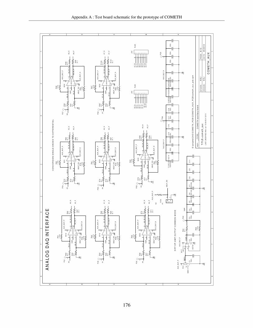
Appendix A : Test board schematic for the prototype of COMETH
176
CO
NV
ER
SIO
N S
ING
LE
-EN
DE
D T
O D
IFF
ER
EN
TIA
L
AN
AL
OG
DA
Q I
NT
ER
FA
CE
CO
ME
TH
_A
UX
05
/20
13
KK
J
KK
J
CO
ME
TH
au
xili
ary
bo
ard
DIF
F O
P-A
MP
OU
TP
UT
CO
MM
ON
MO
DE
LA
ST
_M
OD
IFIE
D=
Mo
n J
un
10
09
:43
:41
20
13
6/1
2
D:\
pro
jets
\CA
O\C
OM
ET
H_
PC
B\C
OM
ET
H_
AU
X_
PC
B\c
om
eth
_a
ux_
pcb
.cp
m
12
TIT
LE
=co
me
th_
au
x
10
0n
51
.1
1.2
1k
10
0n
10
0n
51
1
51
.1
51
15
11
51
1
51
1
1.2
1k
1.2
1k
1.2
1k
51
.1
LM
H6
55
0
1.2
1k
51
.1
LM
H6
55
0
LM
H6
55
0
1k
LM
P7
73
1
1.2
1k
1.2
1k
51
1L
MH
65
50
1.2
1k
51
.1
LM
H6
55
0
1.2
1k
1.2
1k
LM
H6
55
0
1.2
1k
51
.1
51
.1
LM
H6
55
05
11
LM
H6
55
0
51
.1
10
0n
10
0n
10
0n
10
0n
10
0n
10
0n
10
0n
10
0n
10
0n
10
0n
10
0n
10
0n
10
0n
10
0n
10
0n
10
0n
10
0n
1.2
1k
10
0n
10
0n
10
0n
51
.1
51
1
51
1
SM
D1
1T
-D
51
1
51
1
51
1
51
1
51
15
11
1.2
1k
RJ4
5
51
.1
51
.1
SO
T2
3
51
.1 51
.1
51
.1
51
.1
10
0n
51
.1
51
.1
RJ4
5
10
0n
10
0n
1.2
1k
1.2
1k
51
1
1.2
1k
1.2
1k
10
.0k
J61
R25
P5
9P
56
P5
8
P5
7
P5
5
P5
3P5
4
P5
0
P4
9P5
1
J3
4J
33
C1
9C
20
C2
1C
22
C2
3C
24
C2
5C
26
C1
0C
12
C1
3C
14
C1
6C
15
C1
8C
17
C1
1C
9C
8C
7C
6C
5C
4C
3
R1
00
R1
01
R9
7 M2
5R
92
R9
3
R9
5
R9
8 R9
9
R9
6 M2
4R
90
R9
1
R9
4
R8
6
R8
7
R8
1 M2
2R
74
R7
5
R7
9 R8
2
R7
7
R7
6M
23
R8
3
R8
9
R8
8
R7
8
R7
3
R7
2M
21
R8
0
R8
5
R8
4
R6
0
R5
7
R5
6M
20
R6
3
R7
1
R7
0
R5
9
R5
5
R5
4M
19
R6
2
R6
9
R6
8
P5
2
C2
C1
PO
1
R6
5
R6
4M
17
R6
7
R6
6
R5
8
R5
3
R6
1
R5
2M
18
AU
X_
BU
F_
P
A2
_A
AU
X_
BU
F_
P
A5
_IN
_P
A4
_A
A1
_IN
_N
A3
_IN
_N
VM
RA
0_
IN_
N
VM
R
A3
_A
A4
_B AB
UF
_E
N
A5
_A
VM
R
A1
_N
A4
_IN
_N
A4
_N
A7
A6
A3
A2
A0
_A
AU
X_
BU
F_
N
AB
UF
_E
N
A5
_N
A5
_P
A4
_N
A1
_P
A4
_P
A7
_N
A7
_P
A6
_N
A6
_P
A0
_P
A0
_N
AU
X_
BU
F_
P
A2
_P
A2
_N
A3
_P
A3
_N
A7
_N
A7
_P
A7
_IN
_P
A7
_IN
_N
A7
_B
A7
_A
A6
_P
A6
_N
A6
_IN
_P
A6
_IN
_N
A6
_B
A6
_A
A5
_P
A5
_N
A5
_IN
_N
A4
_P
A4
_IN
_P
A3
_B
A3
_IN
_P
A3
_P
AU
X_
BU
F_
P
A2
_P
A2
_N
A0
_BVM
RA
0_
N
A0
_P
VM
RA
AU
X_
BU
F_
P
AU
X_
BU
F_
N
VM
R
AB
UF
_E
N
AB
UF
_E
NA
UX
_B
UF
_N
AU
X_
BU
F_
P
AU
X_
BU
F_
N
VM
R
AB
UF
_E
N
AU
X_
BU
F_
N
AU
X_
BU
F_
P
A0
_IN
_P
VM
R
AB
UF
_E
N
AU
X_
BU
F_
N
A1
_IN
_P
A1
_P
A1
_N
A0
A1
A1
_A
A3
_N
A5
AU
X_
BU
F_
P
VM
R_
IN
AU
X_
BU
F_
P
A5
_B
AU
X_
BU
F_
N
AU
X_
BU
F_
N
A2
_IN
_P
VM
R
A2
_B
A1
_B
VM
R
AU
X_
BU
F_
N
A4
AU
X_
BU
F_
P
AB
UF
_E
N
A2
_IN
_N
AU
X_
BU
F_
P
AB
UF
_E
N
AU
X_
BU
F_
PA
BU
F_
EN
2 1
1
1
11
11
1
111
8 7 6 5 4 3 2 1
8 7 6 5 4 3 2 1
3 6
245
8 1
7
3 6
245
8 1
7
3 6
245
8 1
7
3 6
245
8 1
73 6
245
8 1
7
3 6
245
8 1
7
3 6
245
8 1
7
1
3
2
1
5
31
2
4
3 6
245
8 1
7
GN
D
GN
D
GN
D
* *
*
EN
V-
V+
*
*
*
*
GN
D
* *
*
EN
V-
V+
* *
*
*
GN
D
* *
*
EN
V-
V+
* *
*
GN
D GN
D
*
*
**
EN
V-
V+
*
**
GN
D
*
*
*
*
EN
V-
V+
*
**
GN
D
*
**
EN
V-
V+
* *
**
GN
D
*
**
EN
V-
V+
*
*
*
*
GN
D
**
CON2P
2 1
GN
D*
GN
D
12345678
12345678
GN
D
EN
V-
V+
TIT
RE
EE
PA
GE
:
RE
F:
DA
TE
:D
ES
SIN
:
ET
UD
E:
AA
BCC
D
1
2 233
4 455
6 677
8 8
D
1
B
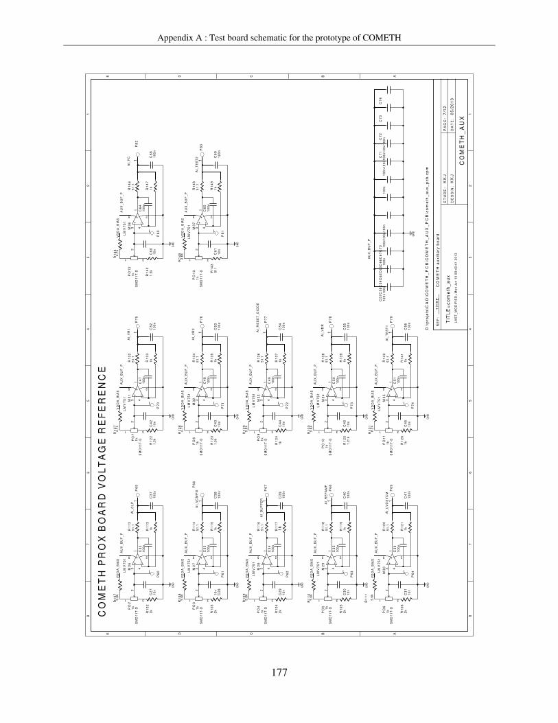
Appendix A : Test board schematic for the prototype of COMETH
177
CO
ME
TH
PR
OX
BO
AR
D V
OL
TA
GE
RE
FE
RE
NC
E
CO
ME
TH
_A
UX
05
/20
13
KK
J
KK
J
CO
ME
TH
au
xili
ary
bo
ard
LA
ST
_M
OD
IFIE
D=
Mo
n J
un
10
09
:43
:41
20
13
7/1
2
D:\
pro
jets
\CA
O\C
OM
ET
H_
PC
B\C
OM
ET
H_
AU
X_
PC
B\c
om
eth
_a
ux_
pcb
.cp
m
TIT
LE
=co
me
th_
au
x
51
.1
51
.1
51
.1
51
.1
51
.1
51
.1
51
.1
51
.1
51
.1
51
.1
51
.1
51
.1
51
1
4.7
k
10
n
10
n1
0n
10
n
10
n
10
n
10
n
10
n
10
n
10
n
10
n
10
n
5.6
k
5.6
k
5.6
k
5.6
k
5.6
k
4.7
k
LM
V7
51
5.6
k
5.6
k
8.2
k
4.7
k
3.6
k
10
0n
10
0n
LM
V7
51
10
0n
1.5
k
SM
D1
1T
-D
10
0n
1.5
k
SM
D1
1T
-D
1k
SM
D1
1T
-D
10
0n
10
0n
10
0n
10
0n
10
0n
10
0n
10
0n
10
0n
10
0n
10
0n
10
0n
10
0n
10
0n
10
0n
1k
10
0n
10
0n
10
0n
10
0n
10
0n
10
0n
10
0n
10
0n
10
0n
10
0n
10
0n
10
0n
10
0n
10
0n
10
0n
10
0n
10
0n
SM
D1
1T
-D1k
2k
LM
V7
51
2k
LM
V7
51
1k
SM
D1
1T
-D
1k
SM
D1
1T
-D
2k
LM
V7
51
1k
1k
1k
1k
1k
1k
1k
1k
1k
1k
2k1
kS
MD
11
T-D
LM
V7
51
1k
SM
D1
1T
-D
2k
LM
V7
51
LM
V7
51
SM
D1
1T
-D1k
1.5
k
1k
LM
V7
51
1k
SM
D1
1T
-D1k
1k
SM
D1
1T
-D
LM
V7
51
1k
SM
D1
1T
-D
1k
LM
V7
51
LM
V7
51
1k
10
0n
1k
1.2
1k
C7
4C
73
C7
2C
71
C5
7C
58
C5
9C
62
C6
3C
66
C6
7C
70
R1
43
PO
13
C6
1
P8
1
R1
45
M3
7
C6
5
R1
49
R1
48
C6
9
P8
3
R1
42
PO
12
C6
0
P8
0
M3
6
R1
44
C6
4
R1
47
R1
46
C6
8
P8
2
R1
26
PO
11
R1
25
PO
10
C4
6
P7
4
M3
5
C5
1
R1
41
R1
31C
45
P7
3
M3
4
R1
40
C5
0
R1
39
R1
38
R1
24
PO
9
R1
23
PO
8
R1
30C
44
R1
29
P7
2
M3
3
R1
37
C4
9
R1
36
C4
3
P7
1
R1
28
M3
2
C4
8
R1
35
R1
34
C5
6
P7
9
C5
5
P7
8
C5
4
P7
7
C5
3
P7
6
R1
22
PO
7
C4
2
P7
0
M3
1
R1
27
C4
7
R1
33
R1
32
C5
2
P7
5
R1
06
PO
6
C3
1
P6
4M3
0
C3
6
R1
21
R1
20
R1
11
C4
1
P6
9
R1
05
PO
5
C3
0
P6
3
R1
10
M2
9
C3
5
R1
19
R1
18
C4
0
P6
8
R1
04
PO
4
C2
9
P6
2
M2
8
R1
09
C3
4
R1
17
R1
16
C3
9
P6
7
R1
03
PO
3
C2
8P
61
M2
7
R1
08
C3
3
R1
15
R1
14
C3
8
P6
6
P6
0
R1
02
PO
2
C2
7
R1
07
M2
6
C3
2
R1
13
R1
12
C3
7
P6
5
VD
DA
_B
IAS
AI_
VR
1
VD
DA
_B
IAS
VD
DA
_B
IAS
AU
X_
BU
F_
P
AU
X_
BU
F_
P
AI_
TE
ST
2
AU
X_
BU
F_
PV
DD
A_
BIA
SA
UX
_B
UF
_P
VD
DA
_B
IAS
AU
X_
BU
F_
P
AU
X_
BU
F_
PV
DD
A_
BIA
S
AI_
LV
DS
VC
M
VD
DA
_B
IAS
AI_
BU
FF
ER
VD
DA
_B
IAS
VD
DA
_B
IAS
AU
X_
BU
F_
P
AI_
CL
P
VD
DA
_B
IAS
AU
X_
BU
F_
P
AU
X_
BU
F_
P
AU
X_
BU
F_
P
AU
X_
BU
F_
P
AU
X_
BU
F_
P
AI_
TE
ST
1
VD
DA
_B
IAS
VD
DA
_B
IAS
AU
X_
BU
F_
P
AI_
VC
MP
IX
AI_
RE
FA
MP
AI_
RE
SE
T_
DIO
DE
AI_
VR
2
AI_
VD
R
AI_
FC
3
2
1
1
5
31
2
41
3
2
1
1
5
31
2
41
3
2
13
2
1
1
5
31
2
41
5
31
24
3
2
13
2
1
1
5
31
2
41
5
31
2
4
1111
3
2
1
1
5
31
2
41
3
2
1
1
5
31
2
41
3
2
1
1
5
31
2
41
3
2
1
1
5
31
2
41
3
2
1
1
5
31
2
41
1
3
2
1
5
31
2
41
*
**
GN
D
*
*
**
*
*
**
GN
D
*
GN
D
**
*
*
GN
D
*
**
*
*
*
***
GN
D
*
*
**
GN
D
GN
D
GN
D
*
GN
D
*
**
*
*
**
GN
D
**
GN
D
*
*
*
GN
D
***
**
*
GN
D
TIT
RE
EE
PA
GE
:
RE
F:
DA
TE
:D
ES
SIN
:
ET
UD
E:
AA
BCC
D
1
2 233
4 455
6 677
8 8
D
1
B

Appendix A : Test board schematic for the prototype of COMETH
178
CO
ME
TH
au
xili
ary
bo
ard
KK
J
KK
J0
5/2
01
3
CO
ME
TH
_A
UX
BIA
S C
UR
RE
NT
: 2
mA
- 4
.6m
A
BIA
S C
UR
RE
NT
: 2
50
uA
-10
00
uA
CO
ME
TH
PR
OX
BO
AR
D C
UR
RE
NT
BIA
S
LA
ST
_M
OD
IFIE
D=
Mo
n J
un
10
09
:43
:41
20
13
D:\
pro
jets
\CA
O\C
OM
ET
H_
PC
B\C
OM
ET
H_
AU
X_
PC
B\c
om
eth
_a
ux_
pcb
.cp
m
8/1
2
1
2
1
21
2
1
2T
ITL
E=
com
eth
_a
ux
10
0n
10
0n
10
0k
2.3
2k
10
0k
10
0n
10
0n
10
0n
10
0n
10
0k
1k
2.3
2k
14
.0k
10
0n
1k
10
0n
10
0k
14
.0k
14
.0k
30
1
1.3
7k
41
2
2.3
2k
1k
R1
57
R1
61
R1
53
J3
8
PO
17
C8
2C
78
R1
56
R1
60
R1
52
J3
7
PO
16
C8
1C
77
R1
55
R1
59
R1
51
J3
6
PO
15
C8
0C
76
C7
5R
15
4R
15
8
R1
50
J3
5
PO
14
C7
9
AI_
AD
RIV
ER
AI_
BIA
S_
OU
T
AI_
SF
BIA
S
AI_
LV
DS
BIA
S
VD
DA
_B
IAS
VD
DA
_B
IAS
VD
DA
_B
IAS
VD
DA
_B
IAS
2
1
3
2
1
2
1
3
2
1
2
1
3
2
1
2
1
3
2
1
**
GN
D
GN
D
*
*
*
GN
D
*
CO
N2
P 2
1
GN
D
**
CO
N2
P 2
1
GN
D
*
CO
N2
P 2
1
GN
D
**
GN
D
*
CO
N2
P 2
1
GN
D
EE
PA
GE
:
RE
F:
DA
TE
:D
ES
SIN
:
ET
UD
E:
AA
BCC
D
1
2 233
4 455
6 677
8 8
D
1
B
TIT
RE
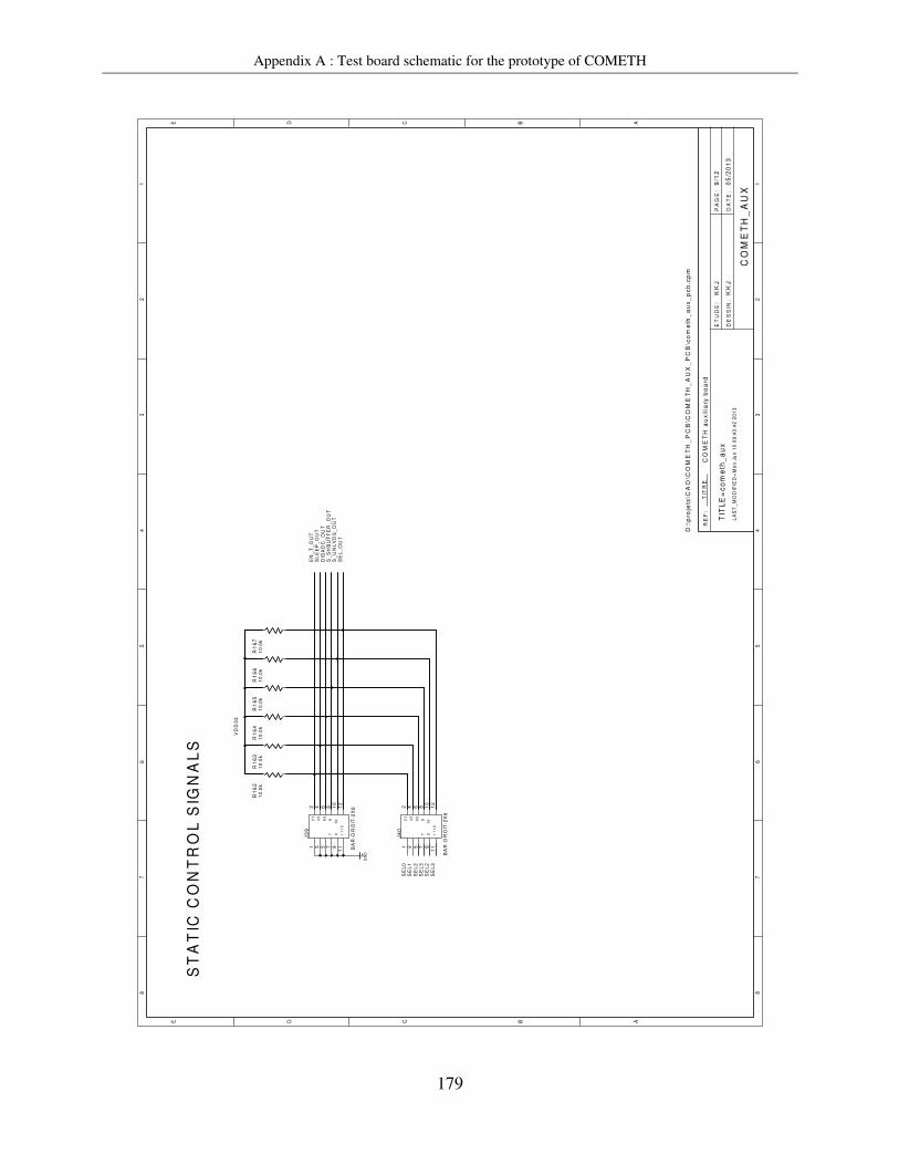
Appendix A : Test board schematic for the prototype of COMETH
179
ST
AT
IC C
ON
TR
OL
SIG
NA
LS
CO
ME
TH
_A
UX
05
/20
13
KK
J
KK
J
CO
ME
TH
au
xili
ary
bo
ard
LA
ST
_M
OD
IFIE
D=
Mo
n J
un
10
09
:43
:42
20
13
D:\
pro
jets
\CA
O\C
OM
ET
H_
PC
B\C
OM
ET
H_
AU
X_
PC
B\c
om
eth
_a
ux_
pcb
.cp
m
9/1
2T
ITL
E=
com
eth
_a
ux
10
.0k
10
.0k
10
.0k
10
.0k
10
.0k
10
.0k
BA
R-D
RO
IT-2
X6
BA
R-D
RO
IT-2
X6
R1
67
R1
66
R1
65
R1
64
R1
63
J4
0
R1
62
J3
9E
N_
T_
OU
T
S_
UN
LV
DS
_O
UT
SE
L3
SE
L2
SE
L3
SE
L2
SE
L1
SE
L0
SL
EE
P_
OU
T
VD
D3
3
DIS
AD
C_
OU
TS
_S
HB
UF
FE
R_
OU
T
SE
L_
OU
T
12
11
10
98
76
54
32
1
12
11
10
98
76
54
32
1
*
*
*
*
*
10
7 9
865
43
21
11
12
*
10
7 9
865
43
21
11
12
GN
D
EE
PA
GE
:
RE
F:
DA
TE
:D
ES
SIN
:
ET
UD
E:
AA
BCC
D
1
2 233
4 455
6 677
8 8
D
1
B
TIT
RE

Appendix A : Test board schematic for the prototype of COMETH
180
KK
J
KK
J0
5/2
01
3
CO
ME
TH
_A
UX
AU
X B
OA
RD
3.3
V
CO
ME
TH
AU
X B
OA
RD
PO
WE
R S
UP
PL
IES
VO
UT
= 1
x (
1 +
R1
/36
5),
VO
UT
= 3
.0V
-3.4
V
3.0
V-3
.4V
, MA
X. 8
00
mA
MA
X. 3
A
CO
ME
TH
au
xili
ary
bo
ard
VO
UT
= -
1.2
1V
x (
1 +
R2
/24
0),
VO
UT
= -
5V
=>
R2
= 7
50
oh
m
MA
X. 1
A
MA
X. 1
A
VO
UT
= 1
.25
x (
1 +
R1
/25
0),
VO
UT
= 5
V =
> R
1 =
75
0o
hm
LA
ST
_M
OD
IFIE
D=
Mo
n J
un
10
09
:43
:40
20
13
10
/12
D:\
pro
jets
\CA
O\C
OM
ET
H_
PC
B\C
OM
ET
H_
AU
X_
PC
B\c
om
eth
_a
ux_
pcb
.cp
m
121
2
12
12
1
2
VIN
BY
PA
SS
SH
TD
N
VO
UT
AD
J
GN
D
VO
UT
SE
NS
ES
D
VIN
1
2
TIT
LE
=co
me
th_
au
x
10
0n
10
0n
10
0n
DA
NG
ER
_BO
ITIE
R
47
u
10
u
10
u
10
u
47
u
LP
38
56
-3V
3
10
.0k
10
.0k
10
.0k
10
.0k
47
u
10
u
10
u
SM
D1
1T
-D
5k
3.0
1k
47
u
(GN
D)
10
n1
0u
GF
1M
_S
47
u4
7u
3A
47
u
10
u4
7u
SO
T2
23
47
uG
F1
M_
S4
7u
CM
S
BA
R-S
ILM
3A
CM
S
75
0
24
0
TO
26
3_
5H
LM
29
91
S
24
9
36
5PS
OP
1.0
0k
LP
38
69
2M
P-A
DJ
1.0
0k
47
u1
0u
10
.0k
47
u4
7u
(GN
D)
BO
ITIE
R=
PO
WE
RIN
_N
75
0
47
u
10
n
P8
P7
P6
P5
P4
P1P
2
P9
P1
0
P3
C15
3C15
4C15
5C15
6R
19
R2
0
M3
9
R1
81
J4
7
C8
3C
85
M3
8 R1
69
PO
18
R1
70
C9
2C
93
R1
71
J4
3
J4
1
R1
68
C1
05
C9
9
M4
1
C9
8
J4
5
R1
77
R1
76
C1
02
C1
04
J4
8
R1
72
C9
7
R1
73
J4
6
C1
03
C1
01
C1
00
R1
75
R1
74
C9
6
M4
0
C8
4
C8
7
C8
8C
91
C9
4C
95
C9
0D
2
J4
4
J4
2
F2
F1
C8
6C
89
D1
AU
X_
BU
F_
P
AU
X_
BU
F_
P_
IN
AU
X_
BU
F_
N
PO
WE
RIN
_N
VD
D3
3
PO
WE
RIN
_PP
OW
ER
IN_
P
PO
WE
RIN
_P
PO
WE
RIN
_N
VD
DA
_B
IAS
PO
WE
RIN
_P
PO
WE
RIN
_P
PO
WE
RIN
_P
VD
D3
3_
SD
AU
X_
BU
F_
N_
IN
VD
DA
_B
IAS
_IN
PO
WE
RIN
_N
VD
D3
3_
SE
NS
E
1
1
1
1
1
1
1
1
1
1
42
51
6
3
321
5
8 4 16
32
1
2
1
2 1
34
1
2
2 1
2
1
2 1
5
2
3
4
1
21
2
1
3 2 12
1
21
21
GN
D
CO
N2P
2
1
+
+
+
+
GN
D
*
GN
D
*
TP
LP
38
56
VIN
SD
SE
NS
E
VO
UT
GN
D
GN
D
*
3
1
2
GN
D
LP
38
78
-AD
J AD
J
VO
UT
SH
TD
N
BY
PA
SS
VIN
*
3 12
*
*
CO
N2P
2
1
GN
D
CON2P
2 1
*
+
+
EN
AA
DJ
OU
TIN
CON2P
2 1
GN
D
GN
D**
CO
N2P
2
1
*
+
GN
D*
+
CON2P
2 1
+
**
GN
D
IN
AD
JG
ND
ON
/OF
F
OU
TL
M2
99
1
+
+
GN
D
+
+
+
TIT
RE
EE
PA
GE
:
RE
F:
DA
TE
:D
ES
SIN
:
ET
UD
E:
AA
BCC
D
1
2 233
4 455
6 677
8 8
D
1
B

Appendix A : Test board schematic for the prototype of COMETH
181
Figure A.2: Schematic of the auxiliary test board of the prototype of COMETH.
CO
ME
TH
PR
OX
BO
AR
D P
OW
ER
SU
PP
LIE
S
3.0
V-3
.4V
, MA
X. 8
00
mA
CO
ME
TH
_A
UX
05
/20
13
KK
J
KK
J
CO
ME
TH
au
xili
ary
bo
ard
1.2
V-1
.9V
, MA
X. 8
00
mA
VO
UT
= -
1.2
1V
x (
1 +
R2
/24
0),
VO
UT
= -
5V
=>
R2
= 7
50
oh
m
5V
, MA
X 1
A
PR
OX
BO
AR
D V
DD
_B
UF
3.3
V
MA
X. 1
A
3.0
V-3
.4V
, MA
X. 8
00
mA
3.0
V-3
.4V
, MA
X. 8
00
mA
-5V
, MA
X 1
A
VO
UT
= 1
.25
x (
1 +
R1
/25
0),
VO
UT
= 5
V =
> R
1 =
75
0o
hm
LA
ST
_M
OD
IFIE
D=
Mo
n J
un
10
10
:39
:11
20
13
D:\
pro
jets
\CA
O\C
OM
ET
H_
PC
B\C
OM
ET
H_
AU
X_
PC
B\c
om
eth
_a
ux_
pcb
.cp
m
11
/12
1
2
1
2
1
2
12
12
VIN
BY
PA
SS
SH
TD
N
VO
UT
AD
J
12
1
2
12
1
2
VIN
BY
PA
SS
SH
TD
N
VO
UT
AD
J
1
2
VIN
BY
PA
SS
SH
TD
N
VO
UT
AD
J
12
VIN
BY
PA
SS
SH
TD
N
VO
UT
AD
J
12
TIT
LE
=co
me
th_
au
x
10
u
LP
38
69
0D
T
SO
T2
23
(GN
D)
LP
38
69
2M
P-A
DJ
75
0
TO
26
3_
5H
LM
29
91
S
BO
ITIE
R=
PO
WE
RIN
_N
36
5
1.0
0k
10
u
24
9
10
.0k
DAN
GE
R_B
OIT
IER
75
0
47
u
47
u
10
0
10
.0k
10
.0k
SM
D1
1T
-D
PS
OP
10
n5
k
10
.0k
24
0
10
u1
0n
1.0
0k
3.0
1k
SM
D1
1T
-D
PS
OP
(GN
D)
10
n1
0u
36
5
47
u
10
.0k
10
u
10
u1
0n
36
5
3.0
1k
5k
10
n1
0u
10
.0k
10
u4
7u
PS
OP
(GND
)
10
u1
0u
47
u
3.3
V
10
u
(GN
D) PS
OP
10
n
36
5
10
n1
.00
k
3.0
1k
(GN
D)
5k
5k
10
u
10
u
10
n3
65
SM
D1
1T
-D
47
u4
7u
SM
D1
1T
-D
47
u4
7u
10
0n
10
0n
10
0n
R1
88
C1
26
C1
31
C1
75
R1
90
C1
23
R1
89
R1
85
C1
17
M4
5
C1
24
R1
87
M4
7
R1
91
C1
77
C1
76
J60
C1
60
C1
59
R2
4P
O2
2
R2
3
R2
1
J2
2M
48
C1
58
C1
57
R2
2
PO
20
PO
19
PO
21
R1
96
R1
93
R1
94
R1
84
R1
95
J5
8
J5
1
C1
09
C1
11
M4
4
R1
80
R1
86
C1
15
J5
4
C1
06
C1
07
M4
2
R1
82
C1
13
C1
12
J5
2J
49
R1
78
C1
10
C1
14
J5
3J
50
R1
79
R1
83
C1
16
C1
08
M4
3
J5
5
C1
20
C1
22
M4
6
C1
19
C1
21
J5
6
R1
92
C1
27
C1
29
C1
32
J5
9
C1
28
C1
18
C1
25
C1
30J
57
AB
UF
_N
PO
WE
RIN
_P
VD
DA
_T
ES
T_
OU
T
VD
D_
BU
F_
IN
PO
WE
RIN
_P
AB
UF
_P
_IN
AB
UF
_P
AB
UF
_N
_IN
PO
WE
RIN
_N
VB
AS
E
PO
WE
RIN
_P
PO
WE
RIN
_P
PO
WE
RIN
_P
VD
DA
_O
UT
VD
DA
PO
WE
RIN
_P
VD
D
VD
DA
_T
ES
T
PO
WE
RIN
_P
PO
WE
RIN
_P
PO
WE
RIN
_P
PO
WE
RIN
_P
PO
WE
RIN
_P
VB
AS
E_
OU
T
PO
WE
RIN
_N
VD
D_
OU
T
VD
D_
BU
F1
5
2
1
3
2
1
3
2
1
2 1
5
8 4 16
3
2
1
3
2
1
3
2
1
321
2 1
5
8 4 16
2
1
5
8 4 16
2
1
2 1
2
1
2 1
5
8 4 16
2 1
34
1
2
2 1
3
4
2
1
2
2
1
*
*
GN
D
CON2P
2 1L
P3
87
8-A
DJ AD
J
VO
UT
SH
TD
N
BY
PA
SS
VIN
*
GN
D
*
*
GN
D
GN
D
*
*
*
GN
D
*
3
1
2
GN
D
CON2P
2 1
GN
D
GN
D
LP
38
78
-AD
J AD
J
VO
UT
SH
TD
N
BY
PA
SS
VIN
*
*
CO
N2P
2
1
GN
D
OU
TIN
GN
D
GN
D
LP
38
78
-AD
J AD
J
VO
UT
SH
TD
N
BY
PA
SS
VIN
*
CO
N2P
2
1
CON2P
2 1
*
CO
N2P 2
1
CON2P
2 1
GN
D
* GN
D
*
*
LP
38
78
-AD
J AD
J
VO
UT
SH
TD
N
BY
PA
SS
VIN
CON2P
2 1
GN
D*
+
+
EN
AA
DJ
OU
TIN
+
CON2P
2 1
GN
D
IN
AD
JG
ND
ON
/OF
F
OU
TL
M2
99
1
GN
D
**
++
CO
N2P
2
1
GN
D**
+
++
+
CO
N2P
2
1
GN
D
*
CO
N2P
2
1
TIT
RE
EE
PA
GE
:
RE
F:
DA
TE
:D
ES
SIN
:
ET
UD
E:
AA
BCC
D
1
2 233
4 455
6 677
8 8
D
1
B

182
Publications:
1. Y. Zhou, J. Baudot, Ch. Hu-Guo, Y. Hu, K. Jasskelainen and M. Winter. COMETH: a CMOS
pixel sensor for highly miniaturized High-flux radiation monitor, Proceedings of Science (PoS)
2014.9
2. Y. Zhou, J. Baudot, C. Duverger, Ch. Hu-Guo, Y. Hu and M. Winter, CMOS Pixel Sensor for
a Space Radiation Monitor with very low cost, power and msss, 2012 JINST 7 C12003.
Communications:
1. Y. Zhou, J. Baudot, Ch. Hu-Guo, Y. Hu, K. Jaaskelainen and M. Winter. COMETH: a CMOS
pixel sensor for a highly miniaturized high-flux radiation monitor, Oral presentation at the
Technology and Instrumentation in Particle Physics (TIPP) conference 2014, 2-6 June,
Amsterdam, Holland.
2. Y. Zhou, J. Baudot, C. Duverger, Ch. Hu-Guo, Y. Hu and M. Winter, Development of a
CMOS Pixel Sensor for Space Radiation Monitor, Poster at l’école IN2P3 de microélectronique
2013, 24-27 June 2013. Porquerolles, France.
3. Y. Zhou, J. Baudot, C. Duverger, Ch. Hu-Guo, Y. Hu and M. Winter. CMOS Pixel Sensor for
a Space Radiation Monitor with very low cost, power and mass, Oral presentation at the 14TH
International Workshop on Radiation Imaging Detectors (IWORID2012), 1-5 July 2012. Figueira
da Foz, Coimbra, Portugal.

183
Abstract
This thesis focuses on the development of a CMOS monolithic pixel sensor used for space
ionizing particles identification and counting in high flux. A new concept for single particle
identification is proposed in this study, which is based on the analysis of particle triggered
clusters. To validate this new concept, a full size sensor including the sensitive pixel matrix, an
analogue signal processing chain, a 3-bit analogue to digital converter, and a digital processing
stage was designed in a 0.35 µm process. The sensor directly output particles flux information
through 4 channels with a very low data rate (80 bps) and minimal power dissipation (~ 100mW).
Each channel represents particles with different species and energies. The highest measurable
flux density is up to 108 particles/cm
2/s (hits pile up < 5%). A reduced scale prototype was
fabricated and tested with 3 types of radiation illumination (X-ray, electrons and infrared laser).
All the results obtained validate the proposed new concept and a highly miniaturized space
radiation monitor based on a single CMOS pixel sensor could be foreseen. The monitor could
provide measurements of comparable or better quality than existing instruments, but at around an
order of magnitude lower power consumption, mass and volume and a lower unit cost. Moreover,
due to its high level and low data rate outputs, no signal treatment power aside the sensor is
required which makes it especially attractive for small satellite application.
Keywords: Highly miniaturized space radiation monitor, CMOS pixel sensor (CPS), Application
Specific Integrated Circuit (ASIC), Partical identification and counting.
184
Résumé
Cette thèse porte sur le développement d'un capteur de pixel monolithique CMOS utilisé pour
l’identification et le comptage des particules ionisés dan l’espace avec un flux élevé. Un nouveau concept pour l’identification de l’espèce des particules proposé dans la présente étude, est basé
sur l'analyse des amas de particules déclenchés. Pour valider ce nouveau concept, un capteur de
taille complet, qui comprend la matrice de pixel sensible aux particules ionisés signal, une chaîne
de traitement du signal analogique, un convertisseur analogue numérique de 3 bits, et un
traitement du signal numérique a été conçu dans un processus de 0.35 µm. Le capteur sortie
directement des informations de flux à travers 4 canaux avec un débit de données très faible
(80 bps) et dissipation d’énergie minimale (~ 100 mW). Chaque canal représente particules avec
différentes espèces et les énergies. La densité maximum de flux mesurable est jusqu'à 108
particules/cm2/s (coups s'accumulent < 5%). Un prototype à échelle réduite a été fabriqué et testé
avec trois types d'illumination de rayonnement (rayons X, les électrons et laser infrarouge). Tous
les résultats obtenus valident le nouveau concept proposé. Un moniteur de rayonnement spatial
très miniaturisé basé sur un capteur de pixel CMOS peut être prévu. Le moniteur peut présente
les mêmes performances que les compteurs actuels, mais avec une dissipation de puissance
réduite d'un ordre de grandeur qu'un poids, un volume d'encombrement et un coût moindre. En
outre, en raison de ses sorties de haut niveau et faible débit de données, aucune traitement
supplémentaire du signal dehors du capteur est nécessaire, ce qui le rend particulièrement
attrayant pour des applications dan les petits satellitaires.
Mots-clés: Très miniaturisé moniteur de rayonnement dans l'espace, CPS (CMOS pixel sensor),
ASIC (Application Specific Integrated Circuit), l'identification et le comptage Partical.