pixel design and evaluation in cmos image sensor...
TRANSCRIPT

Pixel Design and Evaluation in CMOS Image Sensor Technology
S. Vargas-Sierra1, E. Roca, G. Liñán-Cembrano Instituto de Microelectrónica de Sevilla (IMSE), Centro Nacional de Microelectrónica (CNM),
Consejo Superior de Investigaciones Científicas (CSIC) and Universidad de Sevilla Parque Tecnológico de la Cartuja, Calle Américo Vespucio s/n, 41092, Sevilla, Spain
Abstract—A chip designed in a 0.18 μm CMOS Image Sensor Technology (CIS) is presented which incorporates different pixel design alternatives for Active Pixel Sensor (APS). CIS technology improves characteristics such as sensitivity, dark current and noise, that are strongly layout dependent. This chip includes a set of pixel architectures where different parameters have been modified: layout of active diffusion, threshold voltage of the source follower transistor and the use of microlenses. Besides, structures to study the influence of crosstalk between pixels have been incorporated. Keywords— Image Sensors, Active Pixels Sensor, CIS Technology.
I. INTRODUCTION CMOS Image Sensors are presently used in a wide range of
applications, from digital photography to surveillance systems and even toys incorporate them. First CMOS image sensors were developed using standard technologies, emerging as an alternative to CCDs [1][2]. However, the performance of these image sensors in certain applications was poor because they have low sensitivity and large dark current, compared to CCDs specially as technologies scaled down [3][4]. Therefore, foundries incorporated additional steps in their standard CMOS processes to improve sensors performances, developing what are presently known as CMOS Image Sensors Technologies. Additionally, these technologies incorporate post CMOS processing steps that are useful for imaging applications like microlenses and color filters, respectively used to focus the light upon the pixel sensor area and create color images.
During the last few years, different CIS technologies have been developed which include different optimized sensors [6-8]. A first option consists on a process variation where the doping profiles of the photodiode are modified to improve sensitivity and dark current, but keeping the traditional 3-transistors APS (3T-APS) architecture. A second modification introduces the use of pinned photodiodes in a 4-transistors architecture with transfer gate.
It is important to remark that, in these technologies, N-Well and P implant regions are only allowed outside the pixels area; consequently, neither PMOS devices nor substrate contacts are permitted inside pixels. The lack of substrate contacts is compensated by a very low resistance substrate.
Different foundries offer CIS technologies to their customers. However, the performance of their sensors is very dependent on the size and layout of the pixel itself. Therefore, it is strongly recommended to use test chips to optimize pixel design for a given application. For this work, the 3T-APS CIS technology has been selected since it shows lower layout dependence than pinned photodiode technologies.
Section II presents a chip prototype fabricated in the Conventional Photodiode UMC 0.18µm CIS technology (2P4M), where different design parameters have been varied to evaluate their impact on pixel performance. Section III presents the experimental results of this chip and finally some conclusions are drawn out in section IV.
II. CHIP DESIGN In order to optimize the layout of the pixels in this
technology, a chip has been developed which includes 12 arrays of different pixels. These arrays are addressed as parts of a unique sensor array whose dimensions are 256x138. The active row and column are multiplexed and therefore the active pixel is connected to the output buffer, which provides a signal ready to be externally read. Fig. 1 shows the general block diagram of the chip.
The pixels are based on the 3T-APS architecture, where all the transistors are polarized at 3.3V. Fig. 2 shows the schematic of the pixels. It contains a reset transistor (MN1) which precharges the photodiode node to a known voltage; in this case, this voltage would be VDDPIX minus the threshold voltage of the reset transistor. It also includes a row switch (NM2) to connect the source follower (SF1) to the output amplifier structure through the column selecting circuitry.
Preserving the previous circuitry, different pixel designs have been included in the chip taking into account the following parameters:
• Threshold Voltage of Source Follower Transistor • Layout of Active Diffusion • Pixel Size • Crosstalk • Use of Microlenses
1) Threshold Voltage of Source Follower Transistor This technology offers three types of transistors with
different threshold voltage: Zero, Low and Regular Vth. The use of low Vth transistors improves the dynamic range of the sensor, although it might affect the pixel output signal.

Therefore, in this case, pixels with equal layout have been included where the source follower transistor is designed both as a low and as a regular Vth transistor.
2) Layout of Active Diffusion This technology does not allow all type of angles in the
active diffusion layout and its connection to the reset transistor, i.e., there are layout rules for inner and outer angles in these areas. This is because abrupt angles would result in stress and malformation, which would increase non-desirable effects like dark current. Therefore, we have developed the pixels in two shape-like schemes: octagonal and round like. Octagonal-like pixels contain fewer corners in the diffusion shape than round-like ones, but their angles are more abrupt (135º degrees). Round-like ones contain more corners but angles are wider than 135º degrees. Fig. 3 shows the final layouts of the pixels with respect to their active area shape.
3) Pixel Size Two different pixel sizes are used in this work: 3.5x3.5 µm2
and 7x7 µm2. Fig. 3 shows their layout. The first dimension was selected considering a minimum photodiode area that preserved the correct angles and spacing in the connection between the active diffusion and the rest of the circuitry, but could still collect enough light to give high sensitivity values.
4) Crosstalk The pixel would be affected not only by the light incident
directly on it but also by carriers created by light incident on its neighbour pixels that have laterally diffused or by light that scatters through the different overlaying metals until arriving to neighbour pixels. Crosstalk effects can be studied by including arrays of pixels with all, except the central pixel, covered with the top metal and characterizing the response of the array when illuminated. Three different pixel sizes have been included in the chip (3.5µm, 5µm and 7 µm pitch) corresponding to three arrays of 11x11 pixels.
5) Use of Microlenses The microlenses intend to increase sensitivity and minimize
crosstalk between pixels [8]. Its influence in the pixel response is shown in Fig. 4. Microlenses are centred in the middle of the photodiffusion active area and focus the light to this point. They cover a square area, which includes the diffusion and surroundings, but not the entire pixels, as in this technology microlenses are not gapless, i.e. there must be a fixed space between microlenses. Better light collection efficiency is obtained specially for no perpendicular incidence of light. To study the effect of microlenses in this technology, pixels with the same layout with and without microlenses are included in the chip design. An additional crosstalk array with microlenses and pixel size (3.5 µm) has been included.
Table I summarizes all the arrays included indicating their main characteristics and their position in the chip according to the layout shown in Figure 5.
Fig. 2 Pixel schematic diagram.
a) b)
c) d)
Fig. 3 Pixels Layout. a) 3.5 µm Octagonal. b) 3.5 µm Round. c) 7 µm Octagonal. d) 7 µm Round.
Fig. 1 Block Diagram of the Design.

TABLE I ARRAYS INCLUDED IN THE CHIP SUMMARIZED ACCORDING TO THEIR MAIN
CHARACTERISTICS
Arrays Variations between pixels
Array Size
Pixel Size (µm2)
Shape Low Vth
µlenses
1 64x64 3.5x3.5 Round -
2 64x64 3.5x3.5 Round -
3 64x64 3.5x3.5 Octagonal - -
4 64x64 3.5x3.5 Round - -
5 64x64 7x7 Octagonal - -
6 64x64 7x7 Round - -
7 64x64 7x7 Round -
8 64x64 7x7 Round -
9 11x11 3.5x3.5 Round -
10 11x11 3.5x3.5 Round - -
11 11x11 5x5 Round - -
12 11x11 7x7 Round - -
III. EXPERIMENTAL RESULTS In order to test the different arrays included in the chip a
PCB board controlled by a FPGA has been developed. This test board retrieves the pixels voltages, converts them into digital data and stores them. When the frame is completed, the FPGA sends information to a computer to be analysed. This section presents the result of the mathematical analysis.
The test board, where the chip is mounted, has been introduced into an optical bench, which incorporates a visible light source, whose output light power can be varied through a computer controlled power supply. Interference narrow bandpass filters (with FWHM=10nm) centred at wavelengths
ranging from 400-900nm, at 50nm steps, are used to evaluate the spectral response.
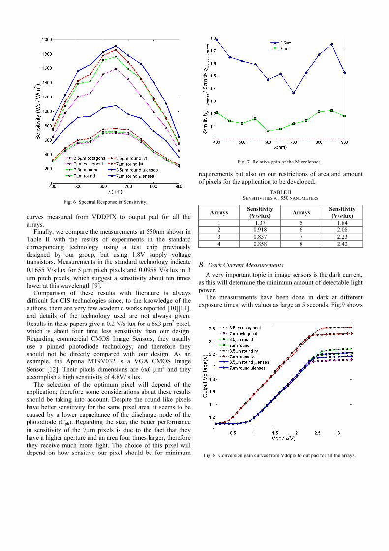
A. Sensitivity Measurements Fig. 6 shows the sensitivity measurements. First, it is
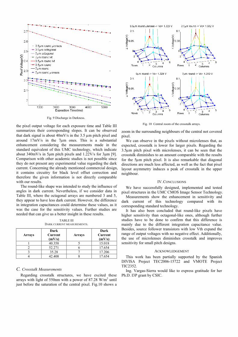
noticeable that the use of microlenses significantly improves the response of the 3.5µm pitch pixels, and it affects positively in the larger size pixels but at a lower ratio. Fig. 7 shows the ratios in the response with and without microlenses for both sizes. This difference in the microlenses improvement ratio is due to the fact that the sensitive area of the 3.5μm pitch pixel is comparable with the height of metals and passivation layers on top of it. Therefore, the amount of light with large angles of incidence redirected into the sensor area is comparatively higher for this pixel.
Second, the “softer” angles seem to enhance the behaviour, as it is evident that octagonal pixels have the worst sensitivities for both pixel sizes, 3.5µm and 7µm. However, this phenomenon could be explained by the active diffusion layout. The area of the octagonal-like active diffusions is slightly higher than the area of the round-like ones, and therefore there is a difference in the integrating capacitance. If the pixels produce the same photogenerated current, a higher capacitance will show a lower voltage drop. Further studies will be needed in the future to determine the values of the integration capacitances of each pixel.
Third, we have observed that pixels with low threshold voltage transistors in the source follower have very similar sensitivity as the same pixel with regular transistors, with the positive effect of the expansion of the output voltage range in about 0.4 V for both sizes. Fig. 8 depicts the conversion gain
Fig. 5 Overall Layout of the Chip.
Fig. 4 Influence of microlenses in the incident light.
curves measured from VDDPIX to output pad for all the arrays.
Finally, we compare the measurements at 550nm shown in Table II with the results of experiments in the standard corresponding technology using a test chip previously designed by our group, but using 1.8V supply voltage transistors. Measurements in the standard technology indicate 0.1655 V/s·lux for 5 µm pitch pixels and 0.0958 V/s·lux in 3 µm pitch pixels, which suggest a sensitivity about ten times lower at this wavelength [9].
Comparison of these results with literature is always difficult for CIS technologies since, to the knowledge of the authors, there are very few academic works reported [10][11], and details of the technology used are not always given. Results in these papers give a 0.2 V/s·lux for a 6x3 µm2 pixel, which is about four time less sensitivity than our design. Regarding commercial CMOS Image Sensors, they usually use a pinned photodiode technology, and therefore they should not be directly compared with our design. As an example, the Aptina MT9V032 is a VGA CMOS Image Sensor [12]. Their pixels dimensions are 6x6 µm2 and they accomplish a high sensitivity of 4.8V/ s·lux.
The selection of the optimum pixel will depend of the application; therefore some considerations about these results should be taking into account. Despite the round like pixels have better sensitivity for the same pixel area, it seems to be caused by a lower capacitance of the discharge node of the photodiode (Cph). Regarding the size, the better performance in sensitivity of the 7µm pixels is due to the fact that they have a higher aperture and an area four times larger, therefore they receive much more light. The choice of this pixel will depend on how sensitive our pixel should be for minimum
requirements but also on our restrictions of area and amount of pixels for the application to be developed.
TABLE II SENSITIVITIES AT 550 NANOMETERS
Arrays Sensitivity (V/s·lux) Arrays Sensitivity
(V/s·lux) 1 1.37 5 1.84 2 0.918 6 2.08 3 0.837 7 2.23 4 0.858 8 2.42
B. Dark Current Measurements A very important topic in image sensors is the dark current,
as this will determine the minimum amount of detectable light power.
The measurements have been done in dark at different exposure times, with values as large as 5 seconds. Fig.9 shows
Fig. 6 Spectral Response in Sensitivity.
Fig. 7 Relative gain of the Microlenses.
Fig. 8 Conversion gain curves from Vddpix to out pad for all the arrays.
the pixel output voltage for each exposure time and Table III summarizes their corresponding slopes. It can be observed that dark signal is about 40mV/s in the 3.5 µm pitch pixel and around 17mV/s in the 7µm ones. This is a substantial enhancement considering the measurements made in the standard equivalent of this UMC technology, which indicate about 340mV/s in 5μm pitch pixels and 1.22V/s for 3μm [9]. Comparison with other academic studies is not possible since they do not present any experimental value regarding the dark current. Concerning the already mentioned commercial design, it contains circuitry for black level offset correction and therefore the given information is not directly comparable with our results.
The round-like shape was intended to study the influence of angles in dark current. Nevertheless, if we consider data in Table III, where the octagonal arrays are numbered 3 and 5, they appear to have less dark current. However, the difference in integration capacitances could determine these values, as it was the case for the sensitivity values. Further studies are needed that can give us a better insight in these results.
TABLE III DARK CURRENT MEASUREMENTS.
Arrays Dark
Current (mV/s)
Arrays Dark
Current (mV/s)
1 40.358 5 15.018 2 52.271 6 17.654 3 35.28 7 17.206 4 42.408 8 17.654
C. Crosstalk Measurements Regarding crosstalk structures, we have excited these
arrays with light of 550nm with a power of 87.28 W/m2 until just before the saturation of the central pixel. Fig.10 shows a
zoom in the surrounding neighbours of the central not covered pixel.
We can observe in the pixels without microlenses that, as expected, crosstalk is lower for larger pixels. Regarding the 3.5µm pitch pixel with microlenses, it can be seen that the crosstalk diminishes to an amount comparable with the results for the 5µm pitch pixel. It is also remarkable that diagonal directions are much less affected, as well as the fact that pixel layout asymmetry induces a peak of crosstalk in the upper neighbour.
IV. CONCLUSIONS We have successfully designed, implemented and tested
pixel structures in the UMC CMOS Image Sensor Technology. Measurements show the enhancement in sensitivity and
dark current of this technology compared with its corresponding standard technology.
It has also been concluded that round-like pixels have higher sensitivity than octagonal-like ones, although further studies have to be done to confirm that this difference is mainly due to the different integration capacitance value. Besides, source follower transistors with low Vth expand the range of output voltages with no negative effect. Additionally, the use of microlenses diminishes crosstalk and improves sensitivity for small pitch designs.
ACKNOWLEDGEMENT This work has been partially supported by the Spanish
DIVISA Project TEC2006-15722 and VMOTE Project TIC2352.
Ing. Vargas-Sierra would like to express gratitude for her Ph.D. I3P grant by CSIC.
Fig. 10 Central zoom of the crosstalk arrays.
Fig. 9 Discharge in Darkness.

REFERENCES [1] E. R. Fossum, “Active pixel sensors: are CCD’s dinosaurs?,” in
Charge-Coupled Devices and Solid-State Optical Sensors III, Proc. SPIE, vol. 1900, pp. 2-14, 1993.
[2] Fossum, E. R.. "CMOS image sensors: electronic camera-on-a-chip." Electron Devices, IEEE Transactions on, Oct. 1997, Volume: 44 , Issue: 10,pages: 1689 – 1698.
[3] Lule, T., S. Benthien, et al. "Sensitivity of CMOS based imagers and scaling perspectives." Electron Devices, IEEE Transactions on Volume 47, Issue 11, Nov 2000 Pages:2110 - 2122.
[4] Hon-Sum Wong. “Technology and device scaling considerations for CMOS imagers”. Electron Devices, IEEE Transactions, Dec. 1996, Volume: 43 , Issue: 12, pages: 2131 - 2142
[5] Guidash, R. M., T.-H. Lee, et al. “A 0.6 μm CMOS pinned photodiode color imager technology”, IEDM’97 Technical Digest, Vol. 8, pp. 927 – 929, 1997.
[6] Shou-Gwo Wuu, Dun-Nian Yaung, et al. .“High performance 0.25-um CMOS color imager technology with non-silicide source/drain pixel”. Electron Devices Meeting, 2000. IEDM Technical Digest. International, 10-13 Dec. 2000, pages: 705 – 708.
[7] Shou-Gwo Wuu, Ho-Ching Chien, et al. “A high performance active pixel sensor with 0.18um CMOS color imager technology”. Electron Devices Meeting, 2001. IEDM Technical Digest. International, 2-5 Dec. 2001, pages: 24.3.1 - 24.3.4
[8] Christian C. Fesenmaier, Yijie Huo, and Peter B. Catrysse. “Optical confinement methods for continued scaling of CMOS image sensor pixels”. 8 December 2008 / Vol. 16, No. 25 / OPTICS EXPRESS.
[9] Alexandre Barajas, Betsaida “Caracterización de Sensores de Imagen en una tecnología CMOS de 0.18µm”. Dissertation presented as partial fulfillment of the requirements for the “Diploma of Advanced Studies” , University of Seville, October 2007.
[10] Blanco-Filgueira, B. Lopez, P. Cabello, D. Ernst, J. Neubauer, H. Hauer, J. “Bottom collection of photodiode-based CMOS APS”, Advanced Semiconductor Devices and Microsystems, 2008. 12-16 Oct. 2008, pages: 67 – 70.
[11] Blanco-Filgueira, B. Lopez, P. Cabello, D. Ernst, J. Neubauer, H. Hauer, J. “Modeling and simulation of CMOS APS” Electron Devices, 2009. 11-13 Feb. 2009, pages: 120 – 123
[12] Aptina MT9V032 Product Flyer , “1/3-Inch, Wide VGA CMOS Image Sensor” .
[13] Ching-Chun Wang. “A Study of CMOS Technologies for Image Sensor Applications”. Ph.D. dissertation, Massachusetts Institute of Technology, August 2001
[14] Shcherback, I., Yadid-Pecht,O. “Photoresponse analysis and pixel shape optimization for CMOS active pixel sensors”, Electron Devices, IEEE Transactions on Volume 50, Issue 1, Jan 2003 Pages: 12 – 18 .