design and optimization of tmo- reram based synaptic devices
TRANSCRIPT

2015 SPICE Workshop June 29-July 3 2015 Mainz, Germany 1
Design and Optimization of TMO-
ReRAM Based Synaptic Devices
J.F. Kang1#, B. Gao1, P. Huang1, Z. Chen1, L.F. Liu1,
X.Y. Liu1, S.M. Yu2, H.-S. P. Wong3
#E-mail: [email protected]
1Institute of Microelectronics, Peking University
2School of CIDSE, Arizona State University
3Department of Electrical Engineering, Stanford University

2015 SPICE Workshop June 29-July 3 2015 Mainz, Germany 2
Outline
Introduction
Physical Mechanism
Defect Engineering Approach
Optimization of Synapse
Summary

2015 SPICE Workshop June 29-July 3 2015 Mainz, Germany 3
Outline
Introduction
Physical Mechanism
Defect Engineering Approach
Optimization of Synapse
Summary

2015 SPICE Workshop June 29-July 3 2015 Mainz, Germany 4
Resistive Switching (RS)
•Many materials have been used to demonstrate the
reversible bi-stable resistance states (LRS and HRS),
which can be switched by voltage, named as resistive
switching (RS)
RRAM
•These RS materials can be used to
construct a device, with a typical
sandwiched structure, termed as
RRAM (Resistive-switching Random
Access Memory).
Introduction
2015 SPICE Workshop June 29-July 3 2015 Mainz, Germany
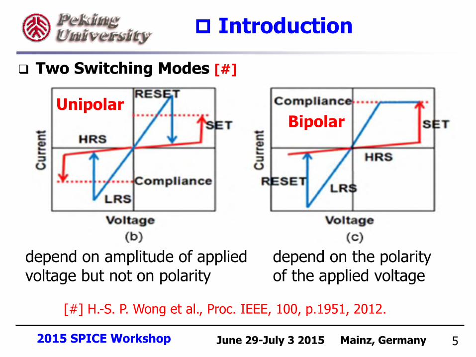
Two Switching Modes [#]
[#] H.-S. P. Wong et al., Proc. IEEE, 100, p.1951, 2012.
5
Unipolar Bipolar
Introduction
depend on amplitude of applied voltage but not on polarity
depend on the polarity of the applied voltage
2015 SPICE Workshop June 29-July 3 2015 Mainz, Germany 6
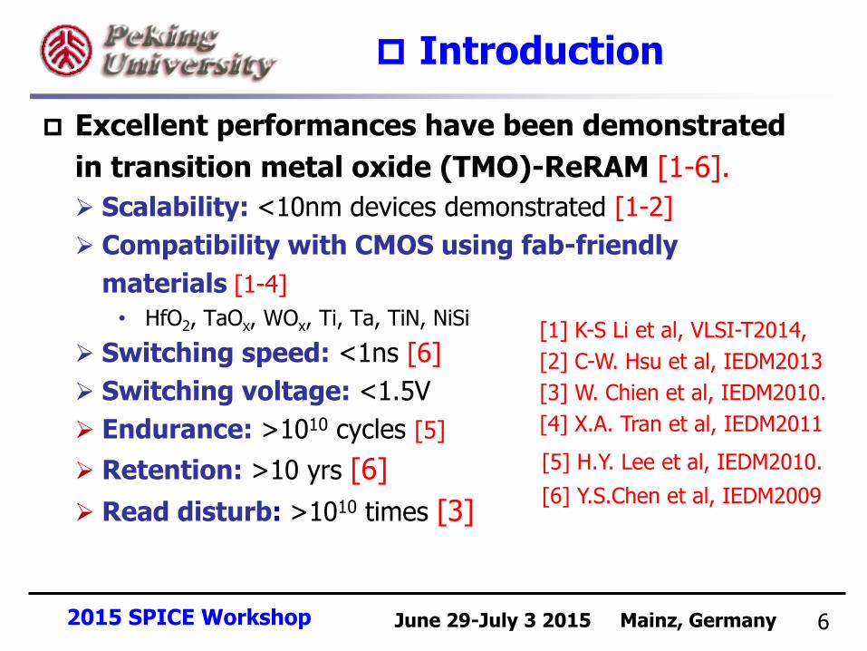
Excellent performances have been demonstrated
in transition metal oxide (TMO)-ReRAM [1-6].
Scalability: <10nm devices demonstrated [1-2]
Compatibility with CMOS using fab-friendly
materials [1-4]
• HfO2, TaOx, WOx, Ti, Ta, TiN, NiSi
Switching speed: <1ns [6]
Switching voltage: <1.5V
Endurance: >1010 cycles [5]
Retention: >10 yrs [6]
Read disturb: >1010 times [3]
[1] K-S Li et al, VLSI-T2014,
[2] C-W. Hsu et al, IEDM2013
[3] W. Chien et al, IEDM2010.
[4] X.A. Tran et al, IEDM2011
[5] H.Y. Lee et al, IEDM2010.
[6] Y.S.Chen et al, IEDM2009
Introduction
2015 SPICE Workshop June 29-July 3 2015 Mainz, Germany 7
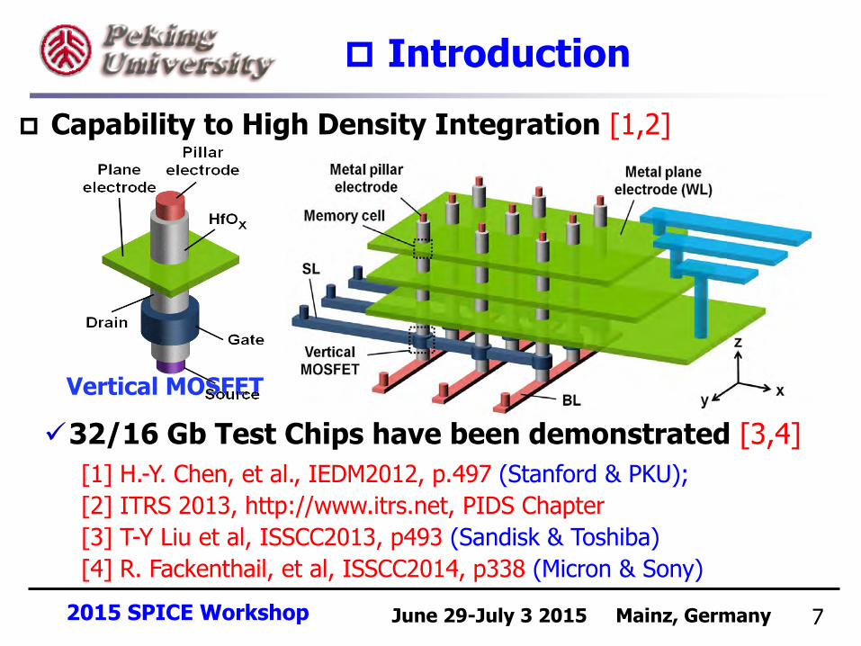
Capability to High Density Integration [1,2]
[1] H.-Y. Chen, et al., IEDM2012, p.497 (Stanford & PKU);
[2] ITRS 2013, http://www.itrs.net, PIDS Chapter
[3] T-Y Liu et al, ISSCC2013, p493 (Sandisk & Toshiba)
[4] R. Fackenthail, et al, ISSCC2014, p338 (Micron & Sony)
Introduction
Vertical MOSFET
32/16 Gb Test Chips have been demonstrated [3,4]
2015 SPICE Workshop June 29-July 3 2015 Mainz, Germany 8
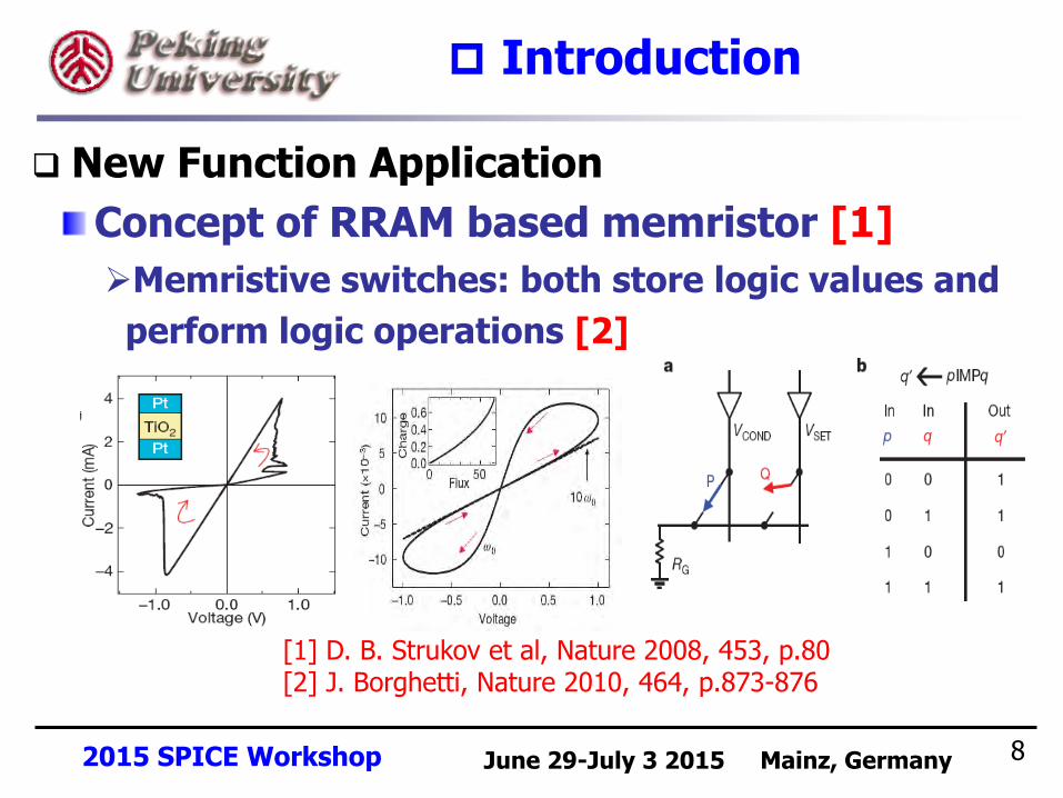
New Function Application
Concept of RRAM based memristor [1]
Memristive switches: both store logic values and
perform logic operations [2]
[1] D. B. Strukov et al, Nature 2008, 453, p.80 [2] J. Borghetti, Nature 2010, 464, p.873-876
Introduction

2015 SPICE Workshop June 29-July 3 2015 Mainz, Germany 9
RRAM based synapses for neuromorphic computing systems [#]
Introduction
[#] S.M. Yu et al, IEDM2012, p.239 (Stanford and PKU)
Most demonstrated in the bipolar switching mode
2015 SPICE Workshop June 29-July 3 2015 Mainz, Germany
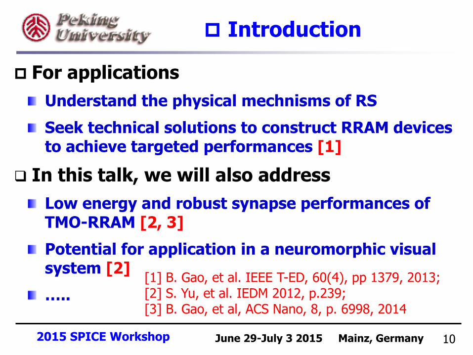
For applications
Understand the physical mechnisms of RS
Seek technical solutions to construct RRAM devices to achieve targeted performances [1]
In this talk, we will also address
Low energy and robust synapse performances of TMO-RRAM [2, 3]
Potential for application in a neuromorphic visual system [2]
…..
Introduction
10
[1] B. Gao, et al. IEEE T-ED, 60(4), pp 1379, 2013; [2] S. Yu, et al. IEDM 2012, p.239; [3] B. Gao, et al, ACS Nano, 8, p. 6998, 2014

2015 SPICE Workshop June 29-July 3 2015 Mainz, Germany 11
Outline
Introduction
Physical Mechanism
Defect Engineering Approach
Optimization of Synapse
Summary
2015 SPICE Workshop June 29-July 3 2015 Mainz, Germany 12
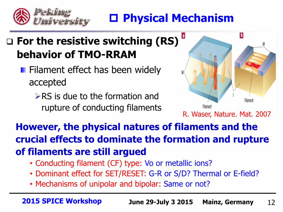
R. Waser, Nature. Mat. 2007
Physical Mechanism
For the resistive switching (RS)
behavior of TMO-RRAM
Filament effect has been widely
accepted
RS is due to the formation and
rupture of conducting filaments
However, the physical natures of filaments and the
crucial effects to dominate the formation and rupture
of filaments are still argued • Conducting filament (CF) type: Vo or metallic ions?
• Dominant effect for SET/RESET: G-R or S/D? Thermal or E-field?
• Mechanisms of unipolar and bipolar: Same or not?
2015 SPICE Workshop June 29-July 3 2015 Mainz, Germany 13
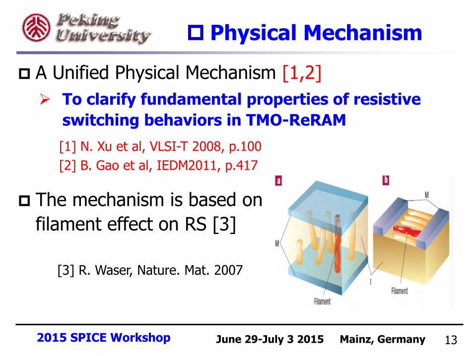
A Unified Physical Mechanism [1,2]
To clarify fundamental properties of resistive
switching behaviors in TMO-ReRAM
Physical Mechanism
The mechanism is based on
filament effect on RS [3]
[3] R. Waser, Nature. Mat. 2007
[1] N. Xu et al, VLSI-T 2008, p.100
[2] B. Gao et al, IEDM2011, p.417

2015 SPICE Workshop June 29-July 3 2015 Mainz, Germany 14
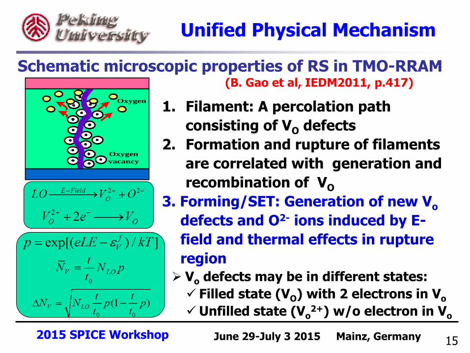
Unified Physical Mechanism
The unified physical mechanism is proposed
to clarify these argued issues:
Microscopic physical properties correlated with
resistive switching in TMO-based RRAM (including
unipolar and bipolar)
To explain various resistive switching
characteristics observed in TMO-RRAM
To predict performances of TMO-RRAM
2015 SPICE Workshop June 29-July 3 2015 Mainz, Germany 15
1. Filament: A percolation path
consisting of VO defects
2. Formation and rupture of filaments
are correlated with generation and
recombination of VO
3. Forming/SET: Generation of new Vo
defects and O2- ions induced by E-
field and thermal effects in rupture
region
Vo defects may be in different states:
Filled state (VO) with 2 electrons in Vo
Unfilled state (Vo2+) w/o electron in Vo
Schematic microscopic properties of RS in TMO-RRAM
Oxygen
Oxygen
vacancy
Unified Physical Mechanism
(B. Gao et al, IEDM2011, p.417)

2015 SPICE Workshop June 29-July 3 2015 Mainz, Germany 16
4. RESET: Recombination
among charged V02+
and O2-
Schematic microscopic properties of RS in TMO-RRAM
Unified Physical Mechanism
5. Two essential conditions for RESET 1) Occurrence of V0
2+ states induced by a critical E-field
2) Presence of moveable O2-
Formation of the state V02+ in the
filament at a critical E-field
significant capture section
stable recombination state (LO)

2015 SPICE Workshop June 29-July 3 2015 Mainz, Germany 17
6. Conduction Properties: due to electron transport along Vo filaments
• Semiconductor-like: Vo are
separated from each other
• Metallic-like: Vo are closed
each other in the clustered
• First principle calculations
support this opinion
Hopping
conduction
Metallic
conduction
Unified Physical Mechanism

2015 SPICE Workshop June 29-July 3 2015 Mainz, Germany 18
Outline
Introduction
Physical Mechanism
Defect Engineering Approach
Optimization of Synapse
Summary

2015 SPICE Workshop June 29-July 3 2015 Mainz, Germany 19
The resistive switching characteristics are
correlated with geometry of Vo filament
generation, recombination, and distributions of
Vo
It is crucial to control Vo distributions and
filament geometry to achieve targeted
performances
2015 SPICE Workshop June 29-July 3 2015 Mainz, Germany 20
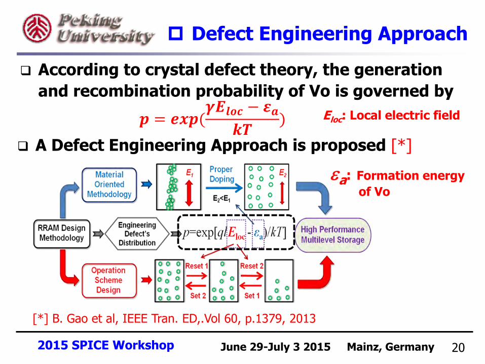
Defect Engineering Approach
According to crystal defect theory, the generation
and recombination probability of Vo is governed by
[*] B. Gao et al, IEEE Tran. ED,.Vol 60, p.1379, 2013
𝒑 = 𝒆𝒙𝒑(𝜸𝑬𝒍𝒐𝒄 − 𝜺𝒂
𝒌𝑻)
A Defect Engineering Approach is proposed [*]
Eloc: Local electric field
a: Formation energy
of Vo

2015 SPICE Workshop June 29-July 3 2015 Mainz, Germany 21
Defect Engineering Approach
A. Material-Oriented Cell Design
B. Innovation Operation Scheme
A Defect Engineering Approach is proposed

2015 SPICE Workshop June 29-July 3 2015 Mainz, Germany
Undoped
(eV)
Ti
(eV)
Al
(eV)
La
(eV)
Ga
(eV)
HfO2 6.53/6.40a 6.48 4.09 3.42
ZrO2 6.37/6.09b 6.11 3.66 3.74 3.77
Calculated formation energy a of Vo [1, 2]
a) A. S. Foster et al. PRB 65, 174117(2002) ; b) A. S. Foster et al. PRB 64, 224108(2001) ; c) T. R. Paudel et al. PRB 77, 205202(2008)
22
Trivalent La or Al doping could effectively reduce a
A. Material-Oriented Cell Design
Defect Engineering Approach
[1] H.W. Zhang et al, APL 96, 2010 [2] B. Gao et al, VLSI2009
2015 SPICE Workshop June 29-July 3 2015 Mainz, Germany 23
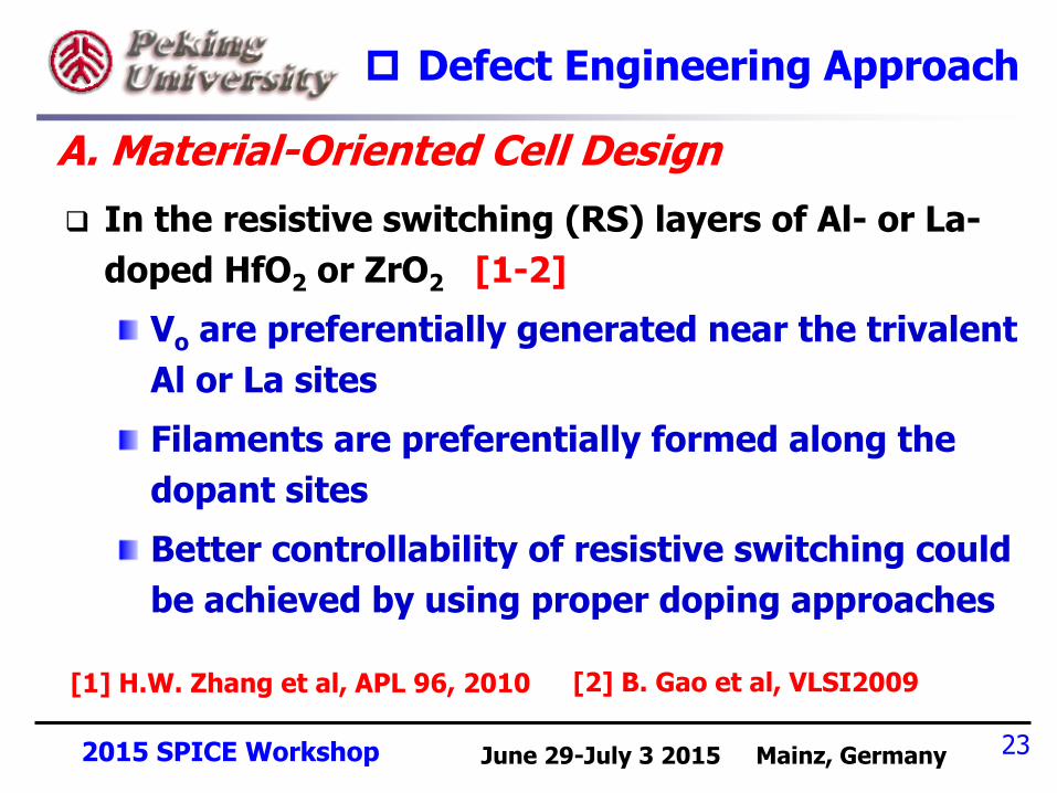
In the resistive switching (RS) layers of Al- or La-
doped HfO2 or ZrO2 [1-2]
Vo are preferentially generated near the trivalent
Al or La sites
Filaments are preferentially formed along the
dopant sites
Better controllability of resistive switching could
be achieved by using proper doping approaches
[1] H.W. Zhang et al, APL 96, 2010 [2] B. Gao et al, VLSI2009
A. Material-Oriented Cell Design
Defect Engineering Approach
2015 SPICE Workshop June 29-July 3 2015 Mainz, Germany 24
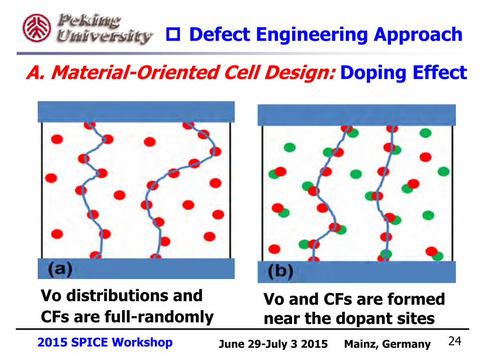
Vo distributions and
CFs are full-randomly Vo and CFs are formed near the dopant sites
A. Material-Oriented Cell Design: Doping Effect
Defect Engineering Approach
2015 SPICE Workshop June 29-July 3 2015 Mainz, Germany 25
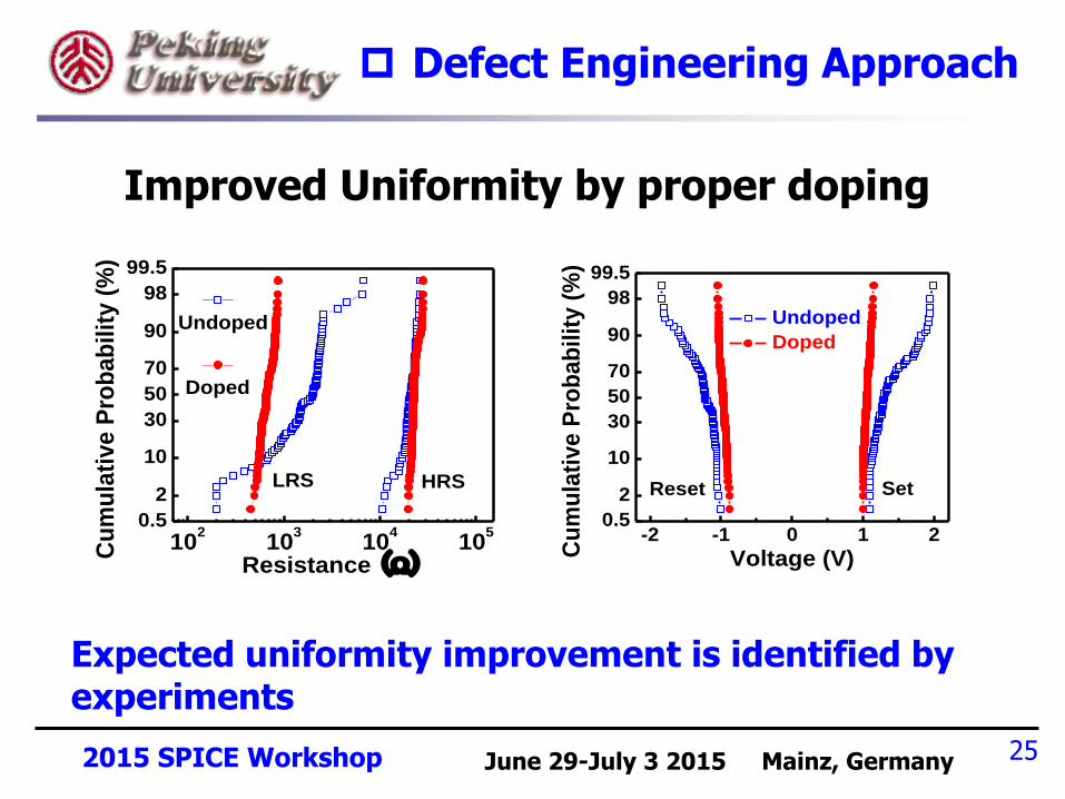
Improved Uniformity by proper doping
Expected uniformity improvement is identified by experiments
102
103
104
105
0.5
2
10
30
50
70
90
98
99.5
Undoped
Doped
HRS
Cu
mu
lati
ve
Pro
bab
ilit
y (
%)
Resistance ()
LRS
-2 -1 0 1 20.5
2
10
30
50
70
90
98
99.5
Set
Undoped
Doped
Cu
mu
lati
ve
Pro
ba
bil
ity
(%
)Voltage (V)
Reset
Defect Engineering Approach
2015 SPICE Workshop June 29-July 3 2015 Mainz, Germany 26
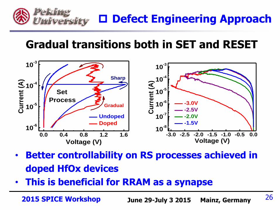
• Better controllability on RS processes achieved in
doped HfOx devices
• This is beneficial for RRAM as a synapse
0.0 0.4 0.8 1.2 1.6
10-6
10-5
10-4
10-3
Sharp
Undoped
Doped
Cu
rre
nt
(A)
Voltage (V)
Set
Process Gradual
-3.0 -2.5 -2.0 -1.5 -1.0 -0.5 0.010
-8
10-7
10-6
10-5
10-4
10-3
-3.0V
-2.5V
-2.0V
-1.5V
Cu
rre
nt
(A)
Voltage (V)
Defect Engineering Approach
Gradual transitions both in SET and RESET

2015 SPICE Workshop June 29-July 3 2015 Mainz, Germany 27
• Vo density is dependent
on local electric field and
switching time
• Operation schemes
(switching time and local
electric field) can be used
to control Vo distributions
Different operation schemes can be expected to achieve different response characteristics!!
Defect Engineering Approach
B. Innovation Operation Scheme

2015 SPICE Workshop June 29-July 3 2015 Mainz, Germany 28
B. Innovation Operation Scheme
Non linear resistance change as a function of pulses is observed when short pulses are applied.
Defect Engineering Approach
2015 SPICE Workshop June 29-July 3 2015 Mainz, Germany 29
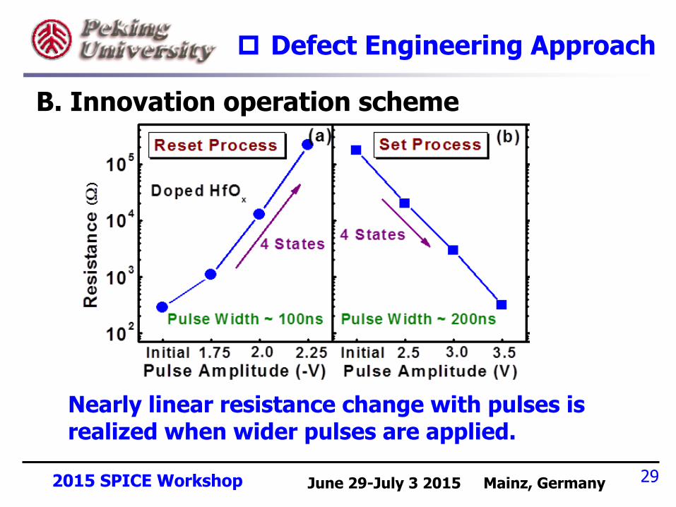
B. Innovation operation scheme
Defect Engineering Approach
Nearly linear resistance change with pulses is realized when wider pulses are applied.

2015 SPICE Workshop June 29-July 3 2015 Mainz, Germany 30
Outline
Introduction
Physical Mechanism
Defect Engineering Approach
Optimization of Synapse
Summary
2015 SPICE Workshop June 29-July 3 2015 Mainz, Germany 31
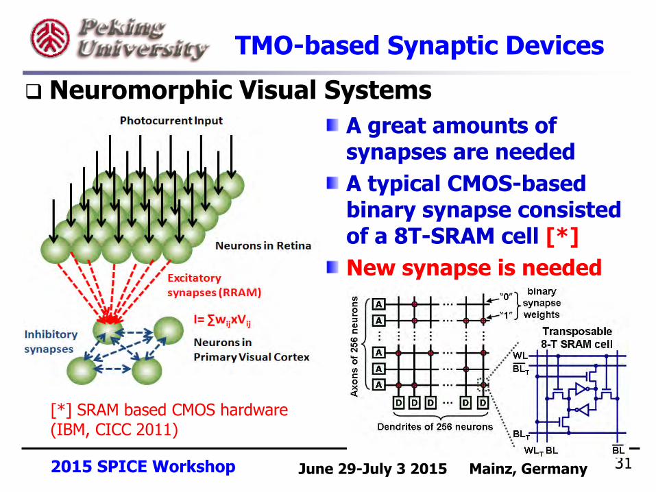
Neuromorphic Visual Systems
[*] SRAM based CMOS hardware (IBM, CICC 2011)
TMO-based Synaptic Devices
A great amounts of synapses are needed
A typical CMOS-based binary synapse consisted of a 8T-SRAM cell [*]
New synapse is needed

2015 SPICE Workshop June 29-July 3 2015 Mainz, Germany
TMO-based Synaptic Devices
Analogy between biological and artificial RRAM synapse.
TMO-RRAM-based synapse is promising
32
Analogy between biological and RRAM based neural networks.

2015 SPICE Workshop June 29-July 3 2015 Mainz, Germany
Artificial Visual System-based on RRAM and Winner-Take-All algorithm is constructed
Integrated-and-fire neuron circuit
1st layer: 32× 32 neurons; 2nd layer: 4× 4 neurons between 1st layer and 2nd layer: 16348 RRAM synapses
33
Optimization of Synapse
2015 SPICE Workshop June 29-July 3 2015 Mainz, Germany
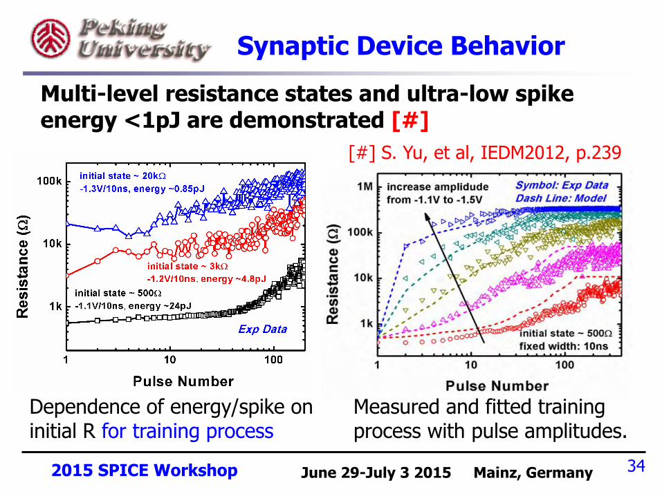
Multi-level resistance states and ultra-low spike energy <1pJ are demonstrated [#]
Dependence of energy/spike on initial R for training process
[#] S. Yu, et al, IEDM2012, p.239
Synaptic Device Behavior
34
Measured and fitted training process with pulse amplitudes.
2015 SPICE Workshop June 29-July 3 2015 Mainz, Germany
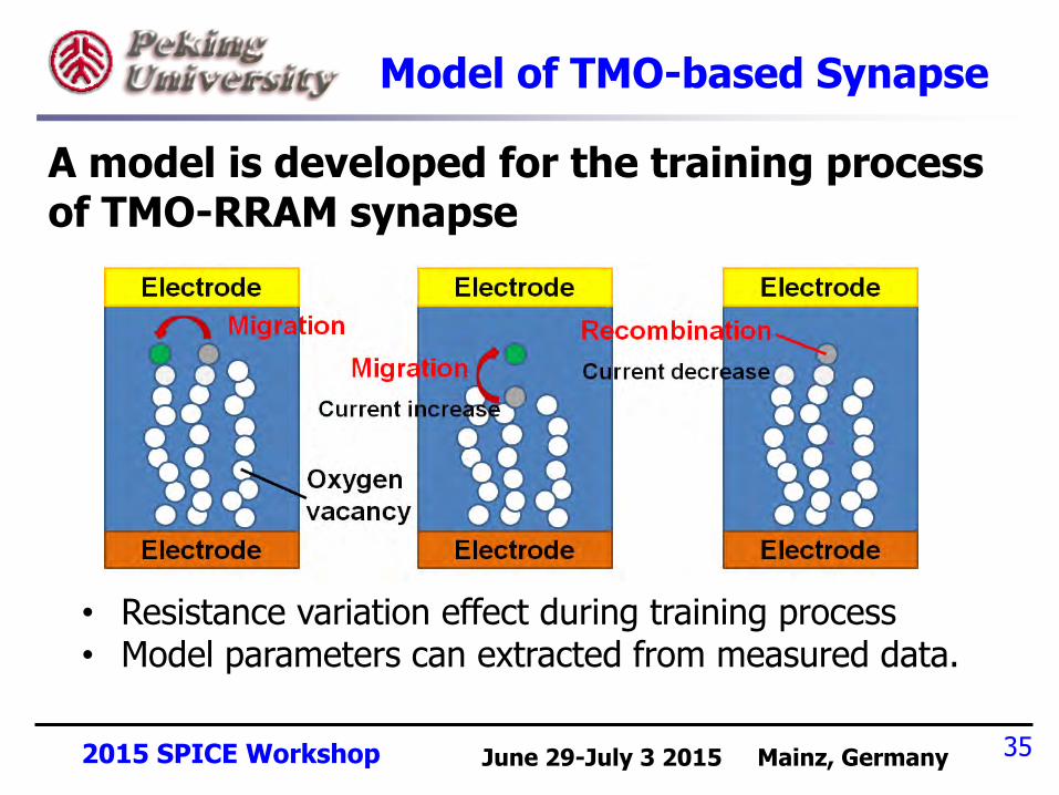
A model is developed for the training process of TMO-RRAM synapse
• Resistance variation effect during training process • Model parameters can extracted from measured data.
Model of TMO-based Synapse
35

2015 SPICE Workshop June 29-July 3 2015 Mainz, Germany
Resistance Evolution under 400 RESET pulses
• In low resistance regime, fluctuation is smaller but suffers from high spike energy
• In high resistance regime, low spike energy but larger fluctuation presented
Larger fluctuation or variation may cause degradation of recognition accuracy of the neuromorphic systems
36
TMO-based Synaptic Devices
2015 SPICE Workshop June 29-July 3 2015 Mainz, Germany
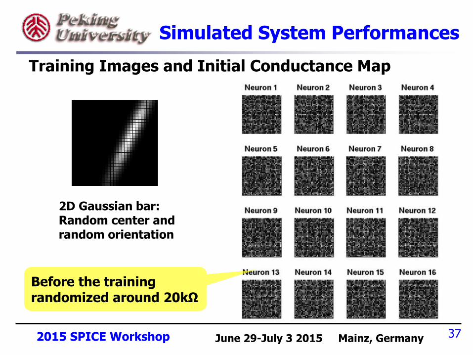
Training Images and Initial Conductance Map
Before the training randomized around 20kΩ
2D Gaussian bar: Random center and random orientation
Simulated System Performances
37
2015 SPICE Workshop June 29-July 3 2015 Mainz, Germany
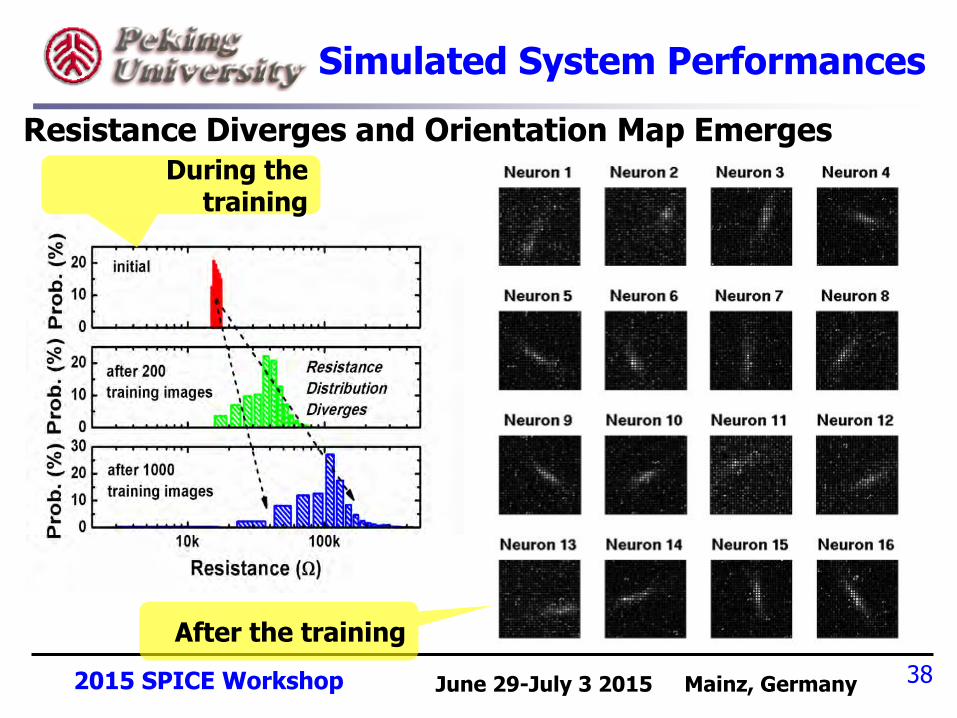
Resistance Diverges and Orientation Map Emerges During the
training
After the training
38
Simulated System Performances

2015 SPICE Workshop June 29-July 3 2015 Mainz, Germany
Optimized Synaptic Devices
Can we realize synaptic performances with both low spike energy and high recognition accuracy ? ?
Geometric mean of more than 2 devices in parallel can significantly suppress the impact of intrinsic fluctuation effect
39

2015 SPICE Workshop June 29-July 3 2015 Mainz, Germany
Optimized Synaptic Devices
Geometric mean calculation on resistance is replaced by the logarithm function.
Optimized architecture of a neuromorphic system using robust synapse is proposed
40
• A 1D1R synaptic cell is
introduced
• 1D is applied to
perform logarithm
function on the device
resistance

2015 SPICE Workshop June 29-July 3 2015 Mainz, Germany
Simulated System Accuracy
• Single RRAM device
• Geometric mean of two devices
• Two parallel 1D-1R cells
• Significant improvement on recognition accuracy is achieved by the architecture of 2 parallel 1D1R.
• Array integration approach is a great challenge
41

2015 SPICE Workshop June 29-July 3 2015 Mainz, Germany
Optimized Synaptic Devices
42
3D vertical ReRAM array architecture as synapses
Easily to achieve high
density of integration
Significantly to
immunize resistance
variation during
training process of
synapses
A synapse: devices in the same pillar electrode

2015 SPICE Workshop June 29-July 3 2015 Mainz, Germany
3D Vertical RRAM Arrays
43
Measured training process of top and bottom ReRAM devices in the 3D vertical array
2 layered devices are
fabricated
Nearly constant device
performance both in
top and bottom layers
is measured.
Significantly improved
accuracy achieved.
2015 SPICE Workshop June 29-July 3 2015 Mainz, Germany
TMO-based Synaptic Devices
44
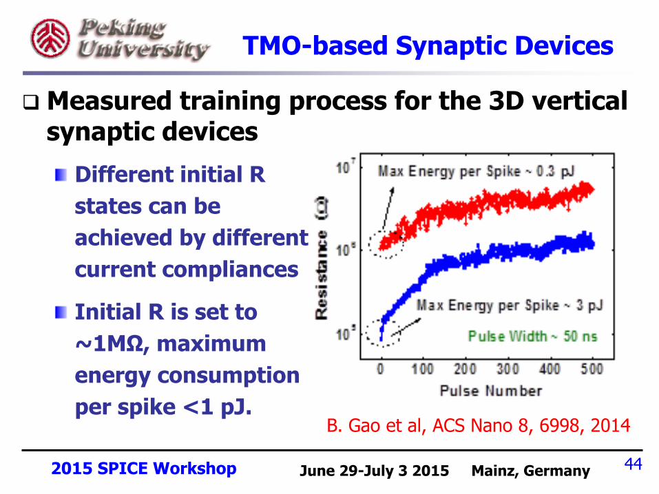
Measured training process for the 3D vertical synaptic devices
Different initial R
states can be
achieved by different
current compliances
Initial R is set to
~1MΩ, maximum
energy consumption
per spike <1 pJ. B. Gao et al, ACS Nano 8, 6998, 2014

2015 SPICE Workshop June 29-July 3 2015 Mainz, Germany 45
Outline
Introduction
Physical Mechanism
Defect Engineering Approach
Optimization of Synapse
Summary
2015 SPICE Workshop June 29-July 3 2015 Mainz, Germany 46
Summary
A unified physical mechanism is proposed to elucidate the resistive switching of TMO-RRAM
A defect engineering approach is developed to design and optimize RRAM performances
Excellent controllability on RS behaviors is demonstrated in optimized RRAM devices based on the defect engineering approach.
2015 SPICE Workshop June 29-July 3 2015 Mainz, Germany 47
Summary
Multi-level resistance states are realized in
the optimized RRAM
Robust synaptic behaviors with sub-pJ
energy per spike are realized in the
optimized RRAM
Optimized architectures of TMO-RRAM
synapse are proposed to improve system
performances.