csim601251 instructor: tim dosen ddak slide by : erdefi
TRANSCRIPT

CSIM601251Instructor: Tim Dosen DDAK
Slide By : Erdefi RakunFasilkom UI

Sequential Logic 2
• Memory Elements
• Latches: S-R Latch, D Latch
• Flip-flops: S-R flip-flop, D flip-flop, J-K flip-flops, T flip-flops
• Asynchronous Inputs
• Synchronous Sequential Circuit Analysis
Note: These slides are taken from Aaron Tan’s slide

Sequential Logic 3
• Two classes of logic circuits– Combinational
– Sequential
• Combinational Circuit– Each output depends entirely
on the immediate (present) inputs.
CombinationalLogic: :inputs outputs: :
◼ Sequential Circuit❑ Each output depends on both
present inputs and state.
Memory
CombinationalLogic: :inputs outputs: :

Sequential Logic 4
• Two types of sequential circuits:– Synchronous: outputs change only at specific time
– Asynchronous: outputs change at any time
• Multivibrator: a class of sequential circuits– Bistable (2 stable states)
– Monostable or one-shot (1 stable state)
– Astable (no stable state)
• Bistable logic devices– Latches and flip-flops.
– They differ in the methods used for changing their state.

Sequential Logic 5
• Memory element: a device which can remember value indefinitely, or change value on command from its inputs.
commandMemory element stored value
Q
◼ Characteristic table:
Command(at time t)
Q(t) Q(t+1)
Set X 1
Reset X 0
0 0Memorise /No Change 1 1
Q(t) or Q: current state
Q(t+1) or Q+: next state

Sequential Logic 6
• Memory element with clock.
• Clock is usually a square wave.
commandMemory
element stored valueQ
clock
Positive edges Negative edges
Positive pulses

Sequential Logic 7
• Two types of triggering/activation– Pulse-triggered
– Edge-triggered
• Pulse-triggered– Latches
– ON = 1, OFF = 0
• Edge-triggered– Flip-flops
– Positive edge-triggered (ON = from 0 to 1; OFF = other time)
– Negative edge-triggered (ON = from 1 to 0; OFF = other time)
Positive edges Negative edges
Positive pulses

Sequential Logic 8
• Memory Elements
• Latches: S-R Latch, D Latch
• Flip-flops: S-R flip-flop, D flip-flop, J-K flip-flops, T flip-flops
• Asynchronous Inputs
• Synchronous Sequential Circuit Analysis
Note: These slides are taken from Aaron Tan’s slide

Sequential Logic 9
• Two inputs: S and R.
• Two complementary outputs: Q and Q'.– When Q = HIGH, we say latch is in SET state.
– When Q = LOW, we say latch is in RESET state.
• For active-high input S-R latch (also known as NOR gate latch)– R = HIGH and S = LOW ➔ Q becomes LOW (RESET state)
– S = HIGH and R = LOW ➔ Q becomes HIGH (SET state)
– Both R and S are LOW ➔No change in output Q
– Both R and S are HIGH ➔Outputs Q and Q' are both LOW (invalid!)
• Drawback: invalid condition exists and must be avoided.

Sequential Logic 10
• Active-high input S-R latch:
R
S
Q
Q'
S R Q Q'
1 0 1 0 initial
0 0 1 0 (afer S=1, R=0)
0 1 0 1
0 0 0 1 (after S=0, R=1)
1 1 0 0 invalid!
1
0
0
1
1
0
0
0
0
1
1
0
0
1
0
0
1
1
0
0
S
R
Q
Q'
• Block diagram:

Sequential Logic 11
• Characteristic table for active-high input S-R latch:
S R Q Q'
0 0 NC NC No change. Latchremained in present state.
1 0 1 0 Latch SET.
0 1 0 1 Latch RESET.
1 1 0 0 Invalid condition.
S
R
Q
Q'
S R Q(t+1)
0 0 Q(t) No change
0 1 0 Reset
1 0 1 Set
1 1 indeterminate
Q(t+1) = ?

Sequential Logic 13
• S-R latch + enable input (EN) and 2 NAND gates → a gated S-R latch.
S
R
Q
Q'
EN
S
EN
R
Q
Q'
◼ Outputs change (if necessary) only when EN is high.

Sequential Logic 14
• Make input R equal to S'→ gated D latch.
• D latch eliminates the undesirable condition of invalid state in the S-R latch.
D
EN
Q
Q'
DQ
Q'
EN

Sequential Logic 15
• When EN is high,
– D = HIGH → latch is SET
– D = LOW → latch is RESET
• Hence when EN is high, Q “follows” the D (data) input.
• Characteristic table:
When EN=1, Q(t+1) = ?
EN D Q(t+1)
1 0 0 Reset
1 1 1 Set
0 X Q(t) No change

Sequential Logic 16
• Memory Elements
• Latches: S-R Latch, D Latch
• Flip-flops: S-R flip-flop, D flip-flop, J-K flip-flops, T flip-flops
• Asynchronous Inputs
• Synchronous Sequential Circuit Analysis
Note: These slides are taken from Aaron Tan’s slide

Sequential Logic 17
• Flip-flops are synchronous bistable devices.
• Output changes state at a specified point on a triggering input called the clock.
• Change state either at the positive (rising) edge, or at the negative (falling) edge of the clock signal.
Positive edges Negative edges
Clock signal

Sequential Logic 18
• S-R flip-flop, D flip-flop, and J-K flip-flop.
• Note the “>” symbol at the clock input.
S
C
R
Q
Q'
D
C
Q
Q'
J
C
K
Q
Q'
Positive edge-triggered flip-flops
S
C
R
Q
Q'
D
C
Q
Q'
J
C
K
Q
Q'
Negative edge-triggered flip-flops

Sequential Logic 19
• S-R flip-flop: On the triggering edge of the clock pulse,– R = HIGH and S = LOW ➔ Q becomes LOW (RESET state)
– S = HIGH and R = LOW ➔ Q becomes HIGH (SET state)
– Both R and S are LOW ➔No change in output Q
– Both R and S are HIGH ➔Invalid!
• Characteristic table of positive edge-triggered S-R flip-flop:
X = irrelevant (“don’t care”)
= clock transition LOW to HIGH
S R CLK Q(t+1) Comments
0 0 X Q(t) No change
0 1 0 Reset
1 0 1 Set
1 1 ? Invalid
S
C
R
Q
Q'

Sequential Logic 20
• D flip-flop: Single input D (data). On the triggering edge of the clock pulse,– D = HIGH ➔ Q becomes HIGH (SET state)
– D = LOW ➔ Q becomes LOW (RESET state)
• Hence, Q “follows” D at the clock edge.
• Convert S-R flip-flop into a D flip-flop: add an inverter.
A positive edge-triggered D flip-flop formed with an S-R flip-flop.
S
C
R
Q
Q'
CLK
DD CLK Q(t+1) Comments
1 1 Set
0 0 Reset
= clock transition LOW to HIGH

Sequential Logic 21
• Application: Parallel data transfer.– To transfer logic-circuit outputs X, Y, Z to flip-flops Q1, Q2 and
Q3 for storage.
* After occurrence of negative-going transition
Q1 = X*D
CLK
Q
Q'
Q2 = Y*D
CLK
Q
Q'
Q3 = Z*D
CLK
Q
Q'
Combinational logic circuit
Transfer
X
Y
Z

Sequential Logic 22
• J-K flip-flop: Q and Q' are fed back to the pulse-steering NAND gates.
• No invalid state.
• Include a toggle state– J = HIGH and K = LOW ➔ Q becomes HIGH (SET state)
– K = HIGH and J = LOW ➔ Q becomes LOW (RESET state)
– Both J and K are LOW ➔No change in output Q
– Both J and K are HIGH ➔Toggle

Sequential Logic 23
• J-K flip-flop circuit:
J
Q
Q'
CLK
Pulse transition detector
K
◼ Characteristic table:
J K CLK Q(t+1) Comments
0 0 Q(t) No change
0 1 0 Reset
1 0 1 Set
1 1 Q(t)' Toggle
Q J K Q(t+1)
0 0 0 0
0 0 1 0
0 1 0 1
0 1 1 1
1 0 0 1
1 0 1 0
1 1 0 1
1 1 1 0Q(t+1) = ?

Sequential Logic 24
• T flip-flop: Single input version of the J-K flip-flop, formed by tying both inputs together.
◼ Characteristic table:
TQ
Q'
CLK
Pulse transition detector
J
C
K
Q
Q'
CLK
T
T CLK Q(t+1) Comments
0 Q(t) No change
1 Q(t)' Toggle
Q T Q(t+1)
0 0 0
0 1 1
1 0 1
1 1 0
Q(t+1) = ?

• Use the characteristic tables to find the output waveforms for the flip-flops shown:
T
C
Clock
D,T
QD
QT
D
C
25Sequential Design

• Use the characteristic tables to find the output waveforms for the flip-flops shown:
JC
K
SCR
Clock
S,J
QSR
QJK
R,K
?
26Sequential Design

Sequential Logic 27
• Memory Elements
• Latches: S-R Latch, D Latch
• Flip-flops: S-R flip-flop, D flip-flop, J-K flip-flops, T flip-flops
• Asynchronous Inputs
• Synchronous Sequential Circuit Analysis
Note: These slides are taken from Aaron Tan’s slide

Sequential Logic 28
• S-R, D and J-K inputs are synchronous inputs, as data on these inputs are transferred to the flip-flop’s output only on the triggered edge of the clock pulse.
• Asynchronous inputs affect the state of the flip-flop independent of the clock; example: preset (PRE) and clear(CLR) [or direct set (SD) and direct reset (RD)].
• When PRE=HIGH, Q is immediately set to HIGH.
• When CLR=HIGH, Q is immediately cleared to LOW.
• Flip-flop in normal operation mode when both PRE and CLR are LOW.

Sequential Logic 29
• A J-K flip-flop with active-low PRESET and CLEAR asynchronous inputs.
JQ
Q'
CLK
Pulse transition detector
K
PRE
CLR
J
C
K
Q
Q'
PRE
CLR
PRE
CLR
CLK
QPreset Toggle ClearJ = K = HIGH

Sequential Logic 30
• Memory Elements
• Latches: S-R Latch, D Latch
• Flip-flops: S-R flip-flop, D flip-flop, J-K flip-flops, T flip-flops
• Asynchronous Inputs
• Synchronous Sequential Circuit Analysis
Note: These slides are taken from Aaron Tan’s slide

Sequential Logic 31
• Building blocks: logic gates and flip-flops.
• Flip-flops make up the memory while the gates form one or more combinational subcircuits.
• We have discussed S-R flip-flop, J-K flip-flop, Dflip-flop and T flip-flop.

Sequential Logic 32
• Each type of flip-flop has its own behaviour, shown by its characteristic table.
S R Q(t+1) Comments
0 0 Q(t) No change
0 1 0 Reset
1 0 1 Set
1 1 ? Unpredictable
J K Q(t+1) Comments
0 0 Q(t) No change
0 1 0 Reset
1 0 1 Set
1 1 Q(t)' Toggle
T Q(t+1)
0 Q(t) No change
1 Q(t)' Toggle
D Q(t+1)
0 0 Reset
1 1 Set

Sequential Logic 33
• Given a sequential circuit diagram, we can analyze its behaviour by deriving its state tableand hence its state diagram.
• Requires state equations to be derived for the flip-flop inputs, as well as output functions for the circuit outputs other than the flip-flops (if any).
• We use A(t) and A(t+1) (or simply A and A+) to represent the present state and next state, respectively, of a flip-flop represented by A.

Sequential Logic 34
• Example using D flip-flops
State equations:
A+ = A∙x + B∙x
B+ = A'∙x
Output function:
y = (A + B)∙x'
A
A'
B
B'
y
x
CP
D Q
Q'
D Q
Q'
Figure 1

Sequential Logic 35
• From the state equations and output function, we derive the state table, consisting of all possible binary combinations of present states and inputs.
• State table
– Similar to truth table.
– Inputs and present state on the left side.
– Outputs and next state on the right side.
• m flip-flops and n inputs → 2m+n rows.
Sequential Logic 36
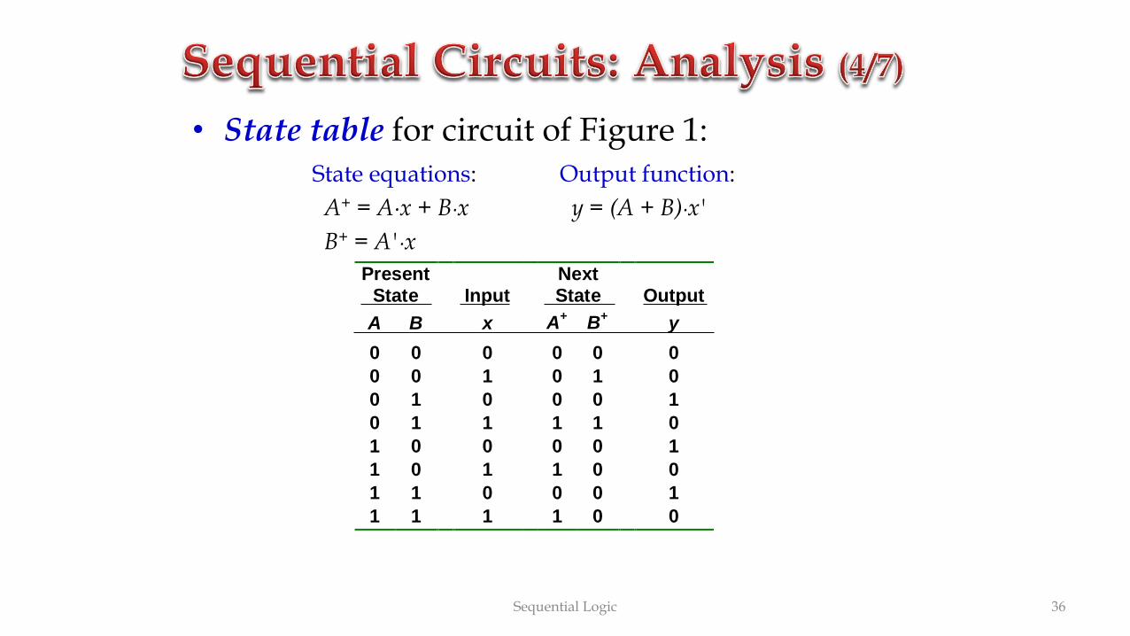
• State table for circuit of Figure 1:State equations:
A+ = A∙x + B∙x
B+ = A'∙x
Output function:
y = (A + B)∙x'
Present NextState Input State Output
A B x A+
B+
y
0 0 0 0 0 0
0 0 1 0 1 0
0 1 0 0 0 1
0 1 1 1 1 0
1 0 0 0 0 1
1 0 1 1 0 0
1 1 0 0 0 1
1 1 1 1 0 0

Sequential Logic 37
• Alternative form of state table:Present Next
State Input State Output
A B x A+
B+ y
0 0 0 0 0 00 0 1 0 1 00 1 0 0 0 10 1 1 1 1 01 0 0 0 0 11 0 1 1 0 01 1 0 0 0 11 1 1 1 0 0
Full table
Present Next State OutputState x=0 x=1 x=0 x=1
AB A+B
+A
+B
+y y
00 00 01 0 0
01 00 11 1 0
10 00 10 1 0
11 00 10 1 0
Compact table

Sequential Logic 38
• From the state table, we can draw the state diagram.
• State diagram– Each state is denoted by a circle.
– Each arrow (between two circles) denotes a transition of the sequential circuit (a row in state table).
– A label of the form a/b is attached to each arrow where a(if there is one) denotes the inputs while b (if there is one) denotes the outputs of the circuit in that transition.
• Each combination of the flip-flop values represents a state. Hence, m flip-flops → up to 2m states.

Sequential Logic 39
• State diagram of the circuit of Figure 1:
Present Next State OutputState x=0 x=1 x=0 x=1
AB A+B
+A
+B
+y y
00 00 01 0 0
01 00 11 1 0
10 00 10 1 0
11 00 10 1 0 00
01 11
10
1/0
1/0
1/0
0/1
0/10/0
1/0 0/1
DONE!

Sequential Logic 40
• The outputs of a sequential circuit are functions of the present states of the flip-flops and the inputs. These are described algebraically by the circuit output functions.
– In Figure 1: y = (A + B)∙x'
• The part of the circuit that generates inputs to the flip-flops are described algebraically by the flip-flop input functions (or flip-flop input equations).
• The flip-flop input functions determine the next state generation.
• From the flip-flop input functions and the characteristic tables of the flip-flops, we obtain the next states of the flip-flops.

Sequential Logic 41
• Example: circuit with a JK flip-flop.
• We use 2 letters to denote each flip-flop input: the first letter denotes the input of the flip-flop (J or K for J-K flip-flop, S or R for S-R flip-flop, D for D flip-flop, T for Tflip-flop) and the second letter denotes the name of the flip-flop.
A
BC'x
By
CP
J Q
Q'K
B'Cx'
JA = B∙C'∙x + B'∙C∙x'
KA = B + y

Sequential Logic 42
• In Figure 1, we obtain the following state equations by observing that Q+ = DQ for a D flip-flop:
A+ = A∙x + B∙x (since DA = A∙x + B∙x)
B+ = A'∙x (since DB = A'∙x)
A
A'
B
B'
y
x
CP
D Q
Q'
D Q
Q'
Figure 1

Sequential Logic 43
• Given Figure 2, a sequential circuit with two J-K flip-flops A and B, and one input x.
A
B
x
CP
J Q
Q'K
J Q
Q'KFigure 2
◼ Obtain the flip-flop input functions from the circuit:
JA = B JB = x'
KA = B∙x' KB = A'∙x + A∙x' = A x

Sequential Logic 44
JA = B JB = x'
KA = B∙x' KB = A'∙x + A∙x' = A x
◼ Fill the state table using the above functions, knowing the characteristics of the flip-flops used.
Present Next state Input state Flip-flop inputs
A B x A+ B+ JA KA JB KB
0 0 0 0 1 0 0 1 0
0 0 1 0 0 0 0 0 1
0 1 0 1 1 1 1 1 0
0 1 1 1 0 1 0 0 1
1 0 0 1 1 0 0 1 1
1 0 1 1 0 0 0 0 0
1 1 0 0 0 1 1 1 1
1 1 1 1 0 1 0 0 0
J K Q(t+1) Comments
0 0 Q(t) No change
0 1 0 Reset
1 0 1 Set
1 1 Q(t)' Toggle

Sequential Logic 45
◼ Draw the state diagram from the state table.
Present Nextstate Input state Flip-flop inputs
A B x A+
B+
JA KA JB KB
0 0 0 0 0 1 0
0 0 1 0 0 0 1
0 1 0 1 1 1 0
0 1 1 1 0 0 1
1 0 0 0 0 1 1
1 0 1 0 0 0 0
1 1 0 1 1 1 1
1 1 1 1 0 0 0

Sequential Logic 46
• Derive the state table and state diagram of this circuit.
◼ Flip-flop input functions:
JA = B JB = KB = (A x)' = A∙x + A'∙x'
KA = B'
J Q
Q'K
J Q
Q'K
A
x
CP
B
y
Figure 3

Sequential Logic 47
• Flip-flop input functions:JA = B JB = KB = (A x)' = A∙x + A'∙x'
KA = B'
• State table:
Present Next state Input state Output Flip-flop inputs
A B x A+ B+ y JA KA JB KB
0 0 0 0 1 0 0 1 1 1
0 0 1 0 0 1 0 1 0 0
0 1 0 1 0 1 1 0 1 1
0 1 1 1 1 0 1 0 0 0
1 0 0 0 0 1 0 1 0 0
1 0 1 0 1 0 0 1 1 1
1 1 0 1 1 0 1 0 0 0
1 1 1 1 0 1 1 0 1 1

Sequential Logic 48
• State diagram:
Present Nextstate Input state Output Flip-flop inputs
A B x A+
B+
y JA KA JB KB
0 0 0 0 0 1 1 1
0 0 1 1 0 1 0 0
0 1 0 1 1 0 1 1
0 1 1 0 1 0 0 0
1 0 0 1 0 1 0 0
1 0 1 0 0 1 1 1
1 1 0 0 1 0 0 0
1 1 1 1 1 0 1 1

Sequential Logic 49
• Analysis: Starting from a circuit diagram, derive the state table or state diagram.
• Design: Starting from a set of specifications (in the form of state equations, state table, or state diagram), derive the logic circuit.
• Characteristic tables are used in analysis.
• Excitation tables are used in design.

Sequential Logic 50
• Excitation tables: given the required transition from present state to next state, determine the flip-flop input(s).
Q Q+
J K
0 0 0 X
0 1 1 X
1 0 X 1
1 1 X 0
JK Flip-flop SR Flip-flop
Q Q+
S R
0 0 0 X
0 1 1 0
1 0 0 1
1 1 X 0
D Flip-flop
Q Q+
D
0 0 0
0 1 1
1 0 0
1 1 1
T Flip-flop
Q Q+
T
0 0 0
0 1 1
1 0 1
1 1 0

Sequential Logic 51
• Design procedure:– Start with circuit specifications – description of circuit
behaviour, usually a state diagram or state table.
– Derive the state table.
– Perform state reduction if necessary.
– Perform state assignment.
– Determine number of flip-flops and label them.
– Choose the type of flip-flop to be used.
– Derive circuit excitation and output tables from the state table.
– Derive circuit output functions and flip-flop input functions.
– Draw the logic diagram.

Sequential Logic 52
• Given the following state diagram, design the sequential circuit using JK flip-flops.
00
10
110
0
0
01
11
1
01
Questions:
How many flip-flops are needed?
How many input variable are there?

Sequential Logic 53
• Circuit state/excitation table, using JK flip-flops.
00
10
11
0
0
0
0 1
111
01
Present Next StateState x=0 x=1
AB A+B
+A
+B
+
00 00 0101 10 0110 10 1111 11 00
Q Q+
J K
0 0 0 X
0 1 1 X
1 0 X 1
1 1 X 0
JK Flip-flop’sexcitation table.
Present Nextstate Input state Flip-flop inputs
A B x A+ B+ JA KA JB KB
0 0 0 0 00 0 1 0 10 1 0 1 00 1 1 0 11 0 0 1 01 0 1 1 11 1 0 1 11 1 1 0 0

Sequential Logic 54
• Block diagram.
Combinationalcircuit
A'ABB'
x
KA JA KB JB
BB'AA'
Externalinput(s)
CP
Externaloutput(s)(none)
J
QQ'
K J
QQ'
K
What are to go in here?
Sequential Logic 55
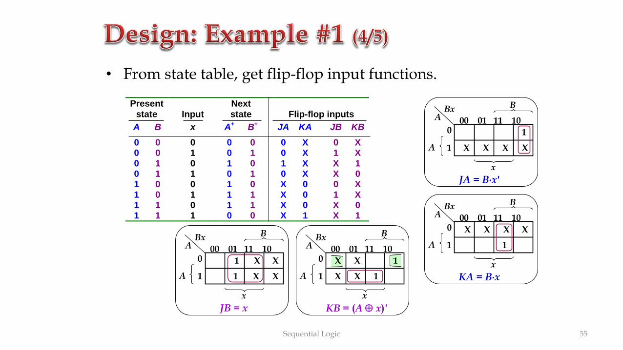
• From state table, get flip-flop input functions.
Present Nextstate Input state Flip-flop inputs
A B x A+ B+ JA KA JB KB
0 0 0 0 0 0 X 0 X0 0 1 0 1 0 X 1 X0 1 0 1 0 1 X X 10 1 1 0 1 0 X X 01 0 0 1 0 X 0 0 X1 0 1 1 1 X 0 1 X1 1 0 1 1 X 0 X 01 1 1 0 0 X 1 X 1
A
B
0
1
00 01 11 10
x
ABx
X X X X
1
JA = B∙x'
JB = x
A
B
0
1
00 01 11 10
x
ABx
X
1 X X
X1
KA = B∙x
A
B
0
1
00 01 11 10
x
ABx
X
1
X XX
KB = (A x)'
A
B
0
1
00 01 11 10
x
ABx
X 1
X 1X
X

Sequential Logic 56
• Flip-flop input functions: JA = B∙x' JB = x
KA = B∙x KB = (A x)'
• Logic diagram:
x
BA
CP
J
QQ'
K J
QQ'
K

Sequential Logic 57
• Using D flip-flops, design the circuit based on the state table below. (Exercise: Design it using JK flip-flops.)
Present Nextstate Input state Output
A B x A+ B+ y
0 0 0 0 0 00 0 1 0 1 10 1 0 1 0 00 1 1 0 1 01 0 0 1 0 01 0 1 1 1 11 1 0 1 1 01 1 1 0 0 0

Sequential Logic 58
• Determine expressions for flip-flop inputs and the circuit output y.
Present Nextstate Input state Output
A B x A+ B+ y
0 0 0 0 0 00 0 1 0 1 10 1 0 1 0 00 1 1 0 1 01 0 0 1 0 01 0 1 1 1 11 1 0 1 1 01 1 1 0 0 0
DA(A,B,x) = ∑ m(2,4,5,6)
DB(A,B,x) = ∑m(1,3,5,6)
y(A,B,x) = ∑ m(1,5)
A
B
0
1
00 01 11 10
x
ABx
1 1 1
1
A
B
0
1
00 01 11 10
x
ABx
1
1 1
1
A
B
0
1
00 01 11 10
x
ABx
1
1
DA = A∙B' + B∙x'
DB = A'∙x + B'∙x + A∙B∙x'
y = B'∙x

Sequential Logic 59
• From derived expressions, draw logic diagram:
D Q
Q'
D Q
Q'
A
A'
B
B'
y
CP
x
DA = A∙B' + B∙x'
DB = A'∙x + B'∙x + A.B∙x'
y = B'∙x

Sequential Logic 60
• Design involving unused states.
Given these Derive these
0 0 0 0 X X X X X X X X X X
0 0 0 1 X X X X X X X X X X
Unused state 000:
Are there other unused states?

Sequential Logic 61
• From state table, obtain expressions for flip-flop inputs.
SA = ? RA = ?
SB = ? RB = ?
B
A
C
00
01
11
10
00 01 11 10
x
ABCx
1X
X
X
X
X X X
A
C
00
01
11
10
00 01 11 10
x
ABCx
11B
X
X
XX
X
X X
X
XA
C
00
01
11
10
00 01 11 10
x
ABCx
1
B
X
X
X
X
X
X X
X
X
X
A
C
00
01
11
10
00 01 11 10
x
ABCx
B
X
X
X
1
X
X X X
1
X X X X
1

Sequential Logic 62
• From state table, obtain expressions for flip-flop inputs (cont’d).
A
C
00
01
11
10
00 01 11 10
x
ABCx
1
1B
X
X
X
X
X
X X
X
XA
C
00
01
11
10
00 01 11 10
x
ABCx
1
B
X
X
1X
X
X X
1
X
X
B
A
C
00
01
11
10
00 01 11 10
x
ABCx
1
X
X
X
X X X
1
SC = ? RC = ?
y = ?
Sequential Logic 63
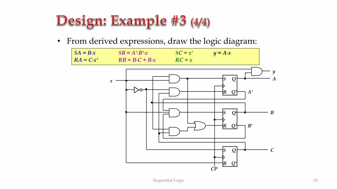
• From derived expressions, draw the logic diagram:
SA = B∙x SB = A'∙B'∙x SC = x' y = A∙x
RA = C∙x' RB = B∙C + B∙x RC = x
A
A'
B
B'
y
CP
x S Q
Q'R
S Q
Q'R
S Q
Q'R
C