cs48l32 - cirrus logic
TRANSCRIPT

CS48L32
Low-Power Audio DSP with Microphone Interface
Features
• Halo Core™ digital signal processor
— Dual MAC, 100 MHz audio signal processor
— 280 kB program memory, 768 kB data memory
— FFT, LMS, and FIR accelerators
• Event logger with time-stamp and interrupt functions
• Integrated multichannel 24-bit audio processor
— 104 dB signal-to-noise ratio (SNR) mic input (16 kHz)
• Programmable wideband, multimic audio processing
• Multichannel isochronous sample-rate conversion
• Up to four analog or digital microphone (DMIC) inputs
• Ultrasonic signal detection and demodulation
• Digital (PDM) output interface
• Two multichannel audio serial ports (ASP), supporting data formats up to 192 kHz, 32 bits
• Flexible clocking configuration, incorporating a low-power frequency-locked loop (FLL)
• Configurable functions on up to 16 general-purpose input/output (GPIO) pins
• Integrated regulator and charge-pump circuits
— Switchable microphone supply/bias outputs
• WLCSP and QFN package variants, 0.4 mm pitch
Applications
• Smartphones and mobile accessories
• Always-on voice-triggered devices
RESET
IRQ ASPn_BCLK Clocking Control
SYSCLK
GPIO
SPI1_SCKSPI1_SS
SPI1_MOSISPI1_MISO
Audio Serial PortsASP1, ASP2
AS
P1
_BC
LK
AS
P1
_F
SY
NC
AS
P1
_D
INA
SP
1_
DO
UT
AS
P2_
BC
LKA
SP
2_
FS
YN
CA
SP
2_
DIN
AS
P2
_D
OU
T
LDO and MICBIAS
Generators
MICBIAS1AMICBIAS1BMICBIAS1C
GND_CP
GND_SUB
VDD_FLLVDD_CP
VREF_FILT
VDD_AGND_A
VDD_IO
GND_D
VDD_D
Input Select
2 x ADC
2 x Stereo Digital Mic Interface
IN1LN_1/IN1_PDMCLKIN1LN_2
IN1LP_1/IN1_PDMDATAIN1LP_2
IN1RN_1/IN2_PDMCLKIN1RN_2
IN1RP_1/IN2_PDMDATAIN1RP_2
Control Interface
SPI
GP
IO2
GP
IO1
Reference Generator
PDM_CLK
Digital Mixing Core
Programmable DSPFive-band equalizer (EQ)
Dynamic range control (DRC)Low-pass/high-pass filter (LHPF)
Isochronous sample -rate conversionUltrasonic demodulatorPWM signal generator
CP_FLYNCP_FLYPCP_FILT
VOUT_MIC
Charge Pump
Auxiliary PDMAUXPDM1–2
AU
XP
DM
1_
CLK
AU
XP
DM
1_
DO
UT
AU
XP
DM
2_
CLK
AU
XP
DM
2_
DO
UT
MC
LK
1
SPI2_SCKSPI2_SS
SPI2_SIO0SPI2_SIO1Quad-SPI
Master Interface
SPI2_SIO2SPI2_SIO3
CS48L32
Cirrus Logic Copyright Cirrus Logic, Inc. 2018–2019
(All Rights Reserved)http://www.cirrus.com
DS1219F4NOV 2019

CS48L32
Description
The CS48L32 is a high-performance low-power audio DSP for smartphones and other portable audio devices. The CS48L32 combines a programmable Halo Core DSP with a variety of power-efficient fixed-function audio processors.
The Halo Core DSP supports multiple concurrent audio features, including voice-trigger detection, noise reduction, media enhancement, and many more. Support for third-party DSP programming provides far-reaching opportunities for product differentiation. The Halo Core DSP is integrated within a fully flexible, all-digital mixing and routing engine with sample rate converters, for wide use-case flexibility.
The CS48L32 supports up to four analog inputs or up to four PDM digital inputs. Low-power input modes are available for always-on (e.g., voice-trigger) functionality using either analog or digital input. Two further digital audio serial ports are provided, each supporting a wide range of standard audio sample rates and serial interface formats.
The audio serial port (ASP) interfaces support multichannel, 32-bit operation at sample rates up to 192 kHz. The integrated FLL provides support for a wide range of system-clock frequencies.
The CS48L32 is configured using the SPI™ interface. The device is powered from 1.8 V and 1.2 V supplies. The power, clocking, and output driver architectures are designed to maximize battery life in voice, music, and standby modes.
Table of Contents
1 Pin Descriptions . . . . . . . . . . . . . . . . . . . . . . . . . . . . . . . . . . . . . 31.1 WLCSP Pinout . . . . . . . . . . . . . . . . . . . . . . . . . . . . . . . . . . . . 31.2 QFN Pinout . . . . . . . . . . . . . . . . . . . . . . . . . . . . . . . . . . . . . . 41.3 Pin Descriptions . . . . . . . . . . . . . . . . . . . . . . . . . . . . . . . . . . . 4
2 Typical Connection Diagram . . . . . . . . . . . . . . . . . . . . . . . . . . . 73 Characteristics and Specifications . . . . . . . . . . . . . . . . . . . . . . 8
Table 3-1. Parameter Definitions . . . . . . . . . . . . . . . . . . . . . . . . . . . . . . . . . . . . . . . . . . . 8Table 3-2. Absolute Maximum Ratings . . . . . . . . . . . . . . . . . . . . . . . . . . . . . . . . . . . . . . . 8Table 3-3. Recommended Operating Conditions . . . . . . . . . . . . . . . . . . . . . . . . . . . . . . . 9Table 3-4. Analog Input Signal Level—IN1xx . . . . . . . . . . . . . . . . . . . . . . . . . . . . . . . . . . 9Table 3-5. Analog Input Pin Characteristics . . . . . . . . . . . . . . . . . . . . . . . . . . . . . . . . . . . 9Table 3-6. Analog Input Gain—Programmable Gain Amplifiers (PGAs) . . . . . . . . . . . . . . 9Table 3-7. Digital Input Signal Level—INn_PDMDATA . . . . . . . . . . . . . . . . . . . . . . . . . . . 9Table 3-8. Input Path Characteristics . . . . . . . . . . . . . . . . . . . . . . . . . . . . . . . . . . . . . . . 10Table 3-9. Digital Input/Output . . . . . . . . . . . . . . . . . . . . . . . . . . . . . . . . . . . . . . . . . . . . 11Table 3-10. Miscellaneous Characteristics . . . . . . . . . . . . . . . . . . . . . . . . . . . . . . . . . . . 12Table 3-11. Device Reset Thresholds . . . . . . . . . . . . . . . . . . . . . . . . . . . . . . . . . . . . . . . 12Table 3-12. System Clock and Frequency-Locked Loop (FLL) . . . . . . . . . . . . . . . . . . . . 13Table 3-13. Digital Input (PDM/DMIC) Interface Timing . . . . . . . . . . . . . . . . . . . . . . . . . 13Table 3-14. AUX PDM Interface Timing . . . . . . . . . . . . . . . . . . . . . . . . . . . . . . . . . . . . . 14Table 3-15. Audio Serial Port—Master Mode . . . . . . . . . . . . . . . . . . . . . . . . . . . . . . . . . 15Table 3-16. Audio Serial Port—Slave Mode . . . . . . . . . . . . . . . . . . . . . . . . . . . . . . . . . . 16Table 3-17. Audio Serial Port Timing—TDM Mode . . . . . . . . . . . . . . . . . . . . . . . . . . . . . 17Table 3-18. Control Interface Timing (SPI1 Slave) . . . . . . . . . . . . . . . . . . . . . . . . . . . . . 18Table 3-19. Master Interface Timing (SPI2 Master) . . . . . . . . . . . . . . . . . . . . . . . . . . . . 19Table 3-20. JTAG Interface Timing . . . . . . . . . . . . . . . . . . . . . . . . . . . . . . . . . . . . . . . . . 20Table 3-21. Typical Signal Latency . . . . . . . . . . . . . . . . . . . . . . . . . . . . . . . . . . . . . . . . . 20
4 Functional Description . . . . . . . . . . . . . . . . . . . . . . . . . . . . . . . 214.1 Overview . . . . . . . . . . . . . . . . . . . . . . . . . . . . . . . . . . . . . . . 214.2 Input Signal Path . . . . . . . . . . . . . . . . . . . . . . . . . . . . . . . . . 234.3 Digital Core . . . . . . . . . . . . . . . . . . . . . . . . . . . . . . . . . . . . . . 434.4 DSP Firmware Control . . . . . . . . . . . . . . . . . . . . . . . . . . . . . 724.5 DSP Peripheral Control . . . . . . . . . . . . . . . . . . . . . . . . . . . . 794.6 Audio Serial Port . . . . . . . . . . . . . . . . . . . . . . . . . . . . . . . . 1074.7 Audio Serial Port Control . . . . . . . . . . . . . . . . . . . . . . . . . . 1134.8 Clocking and Sample Rates . . . . . . . . . . . . . . . . . . . . . . . . 1204.9 Interrupts . . . . . . . . . . . . . . . . . . . . . . . . . . . . . . . . . . . . . . 1334.10 General-Purpose I/O . . . . . . . . . . . . . . . . . . . . . . . . . . . . 1374.11 Control Interface . . . . . . . . . . . . . . . . . . . . . . . . . . . . . . . . 1444.12 Charge Pump, Regulators, and Voltage Reference . . . . . 1464.13 JTAG Interface . . . . . . . . . . . . . . . . . . . . . . . . . . . . . . . . . 1494.14 Power-Up and Resets . . . . . . . . . . . . . . . . . . . . . . . . . . . 1504.15 Device ID . . . . . . . . . . . . . . . . . . . . . . . . . . . . . . . . . . . . . 152
5 Applications . . . . . . . . . . . . . . . . . . . . . . . . . . . . . . . . . . . . . . . 1535.1 Recommended External Components . . . . . . . . . . . . . . . . 1535.2 Audio Serial Port Clocking Configurations . . . . . . . . . . . . . 1565.3 PCB Layout Considerations . . . . . . . . . . . . . . . . . . . . . . . . 161
6 Register Map . . . . . . . . . . . . . . . . . . . . . . . . . . . . . . . . . . . . . . 1617 Thermal Characteristics . . . . . . . . . . . . . . . . . . . . . . . . . . . . . 1888 Package Dimensions . . . . . . . . . . . . . . . . . . . . . . . . . . . . . . . . 1899 Ordering Information . . . . . . . . . . . . . . . . . . . . . . . . . . . . . . . . 19110 Revision History . . . . . . . . . . . . . . . . . . . . . . . . . . . . . . . . . . . 191
2 Cirru
s Logic DS1219F4
CS48L321 Pin Descriptions
1 Pin Descriptions
1.1 WLCSP Pinout
Figure 1-1. Top-Down (Through-Package) View—64-ball WLCSP Package
GND_SUB GND_SUB VDD_A GND_A IN1RP_1/IN2_PDMDATA
IN1LP_2 VOUT_MIC GND_CP
VREF_FILT IN1LP_1/IN1_PDMDATA
IN1LN_1/IN1_PDMCLK
IN1RN_1/IN2_PDMCLK
IN1LN_2 MICBIAS1C GND_CP VDD_CP
NC NC NC IN1RP_2 IN1RN_2 MICBIAS1B CP_FLYP CP_FILT
VDD_D SPI2_SS/GPIO11
SPI2_SIO2/GPIO15
ASP2_BCLK/GPIO9
RESET MICBIAS1A CP_FLYN GND_SUB
GND_D SPI2_SCK/GPIO12
AUXPDM1_DOUT
SPI1_SCK ASP1_BCLK/GPIO5
GPIO1 IRQ VDD_FLL
SPI2_SIO1/GPIO14
AUXPDM2_CLK AUXPDM1_CLK SPI1_MOSI ASP2_FSYNC/GPIO10
ASP1_FSYNC/GPIO6
GPIO2 NC
SPI2_SIO0/GPIO13
AUXPDM2_DOUT
GND_D SPI1_SS ASP2_DOUT/GPIO7
GND_D ASP1_DOUT/GPIO3
MCLK1
NC SPI2_SIO3/GPIO16
VDD_IO SPI1_MISO ASP2_DIN/GPIO8
VDD_D ASP1_DIN/GPIO4
NC
A1 A2 A3 A4 A5 A6 A7 A8
B1 B2 B3 B4 B5 B6 B7 B8
C1 C2 C3 C4 C5 C6 C7 C8
D1 D2 D3 D4 D5 D6 D7 D8
E1 E2 E3 E4 E5 E6 E7 E8
F1 F2 F3 F4 F5 F6 F7 F8
G1 G2 G3 G4 G5 G6 G7 G8
H1 H2 H3 H4 H5 H6 H7 H8
PowerAnalog I/O Digital I/O
3 Cirrus Logic DS1219F4

CS48L321.2 QFN Pinout
1.2 QFN Pinout
Figure 1-2. Top-Down (Through-Package) View—64-pad QFN Package
1.3 Pin Descriptions
Table 1-1 describes each pin on the CS48L32. Note that pins that share a common name should be tied together on the printed circuit board (PCB).
Table 1-1. Pin DescriptionsPU = Pull-up, PD = Pull-down, K = Bus keeper, H = Hysteresis on CMOS input, Z = Hi-Z (High impedance), C = CMOS, OD = Open drain.
Pin NamePin #
(WLCSP)Pin #(QFN)
Power Supply
I/O Pin Description Digital Pad Attributes
State at Reset
Analog I/O
CP_FILT C8 3 — O Charge Pump output decoupling pin — Output
CP_FLYN D7 2 — O Charge Pump fly-back capacitor pin — —
CP_FLYP C7 64 — O Charge Pump fly-back capacitor pin — —
IN1LN_1/IN1_PDMCLK
B3 53 VOUT_MIC or MICBIAS1 [1]
I/O Left-channel negative differential mic/line input/IN1 PDM clock.
C IN1LN_1 input
IN1LN_2 B5 56 VOUT_MIC I Left-channel negative differential mic/line input. — Input
IN1LP_1/IN1_PDMDATA
B2 52 VOUT_MIC or MICBIAS1 [1]
I Left-channel single-ended mic/line input/positive differential mic/line input/IN1 PDM data input.
PD/H IN1LP_1 input
IN1LP_2 A6 57 VOUT_MIC I Left-channel single-ended mic/line input/positive differential mic/line input.
— Input
1
2
3
4
5
6
7
8
9
10
11
12
13
14
15
16
48
47
46
45
44
43
42
41
40
39
38
37
36
35
34
33
4 Cirrus Logic DS1219F4

CS48L321.3 Pin Descriptions
IN1RN_1/IN2_PDMCLK
B4 55 VOUT_MIC or MICBIAS1 [1]
I/O Right-channel negative differential mic/line input/IN2 PDM clock.
C IN1RN_1 input
IN1RN_2 C5 59 VOUT_MIC I Right-channel negative differential mic/line input.
— Input
IN1RP_1/IN2_PDMDATA
A5 54 VOUT_MIC or MICBIAS1 [1]
I Right-channel single-ended mic/line input/positive differential mic/line input/IN2 PDM data input.
PD/H IN1RP_1 input
IN1RP_2 C4 58 VOUT_MIC I Right-channel single-ended mic/line input/positive differential mic/line input.
— Input
MICBIAS1A D6 63 VOUT_MIC O Microphone bias 1A — Output
MICBIAS1B C6 62 VOUT_MIC O Microphone bias 1B — Output
MICBIAS1C B6 61 VOUT_MIC O Microphone bias 1C — Output
VOUT_MIC A7 60 — O LDO2 output decoupling pin (generated internally by CS48L32). Can also be used as reference/supply for external microphones.
— Output
VREF_FILT B1 51 — O Band-gap reference external capacitor connection
— Output
Digital I/O
ASP1_BCLK/GPIO5
E5 17 VDD_IO I/O Audio serial port 1 bit clock/GPIO5 PU/PD/K/H/Z/C/OD
GPIO5 input with bus-keeper
ASP1_DIN/GPIO4
H7 7 VDD_IO I Audio serial port 1 data input/GPIO4 PU/PD/K/H/C/OD
GPIO4 input with bus-keeper
ASP1_DOUT/GPIO3
G7 8 VDD_IO O Audio serial port 1 data output/GPIO3 PU/PD/K/H/Z/C/OD
GPIO3 input with bus-keeper
ASP1_FSYNC/GPIO6
F6 9 VDD_IO I/O Audio serial port 1 frame sync/GPIO6 PU/PD/K/H/Z/C/OD
GPIO6 input with bus-keeper
ASP2_BCLK/GPIO9
D4 22 VDD_IO I/O Audio serial port 2 bit clock/GPIO9 PU/PD/K/H/Z/C/OD
GPIO9 input with bus-keeper
ASP2_DIN/GPIO8
H5 21 VDD_IO I/O Audio serial port 2 data input/GPIO8 PU/PD/K/H/C/OD
GPIO8 input with bus-keeper
ASP2_DOUT/GPIO7
G5 19 VDD_IO I/O Audio serial port 2 data output/GPIO7 PU/PD/K/H/Z/C/OD
GPIO7 input with bus-keeper
ASP2_FSYNC/GPIO10
F5 18 VDD_IO I/O Audio serial port 2 frame sync/GPIO10 PU/PD/K/H/Z/C/OD
GPIO10 input with bus-keeper
AUXPDM1_CLK
F3 28 VDD_IO I/O Auxiliary PDM 1 clock PD/H/C Input
AUXPDM1_DOUT
E3 29 VDD_IO O Auxiliary PDM 1 data output C Output
AUXPDM2_CLK
F2 30 VDD_IO I/O Auxiliary PDM 2 clock PD/H/C Input
AUXPDM2_DOUT
G2 31 VDD_IO O Auxiliary PDM 2 data output C Output
GPIO1 E6 10 VDD_IO I/O GPIO1 PU/PD/K/H/C/OD
GPIO1 input with bus-keeper
GPIO2 F7 16 VDD_IO I/O GPIO2 PU/PD/K/H/C/OD
GPIO2 input with bus-keeper
IRQ E7 5 VDD_IO O Interrupt request (IRQ) output (default is active low)
C/OD Open-drain output
MCLK1 G8 15 VDD_IO I Master clock 1 PD/H Input
RESET D5 4 VDD_IO I Digital reset input (active low) PU/PD/K/H Input with pull-up
Table 1-1. Pin Descriptions (Cont.)PU = Pull-up, PD = Pull-down, K = Bus keeper, H = Hysteresis on CMOS input, Z = Hi-Z (High impedance), C = CMOS, OD = Open drain.
Pin NamePin #
(WLCSP)Pin #(QFN)
Power Supply
I/O Pin Description Digital Pad Attributes
State at Reset
5 Cirrus Logic DS1219F4

CS48L321.3 Pin Descriptions
SPI1_MISO H4 26 VDD_IO O SPI1 control interface Master In Slave Out data. SPI1_MISO is high impedance if SPI1_SS is not asserted.
Z/C Output
SPI1_MOSI F4 24 VDD_IO I SPI1 control interface Master Out Slave In data H/OD Input
SPI1_SCK E4 23 VDD_IO I SPI1 control interface clock input H Input
SPI1_SS G4 25 VDD_IO I SPI1 control interface slave select H Input
SPI2_SCK/GPIO12
E2 41 VDD_IO I/O SPI master interface clock output/GPIO12 PU/PD/K/H/C/OD
GPIO12 input with bus-keeper
SPI2_SIO0/GPIO13
G1 33 VDD_IO I/O SPI master interface Data 0 input/output/GPIO13
PU/PD/K/H/C/OD
GPIO13 input with bus-keeper
SPI2_SIO1/GPIO14
F1 40 VDD_IO I/O SPI master interface Data 1 input/output/GPIO14
PU/PD/K/H/C/OD
GPIO14 input with bus-keeper
SPI2_SIO2/GPIO15
D3 42 VDD_IO I/O SPI master interface Data 2 input/output/GPIO15
PU/PD/K/H/C/OD
GPIO15 input with bus-keeper
SPI2_SIO3/GPIO16
H2 32 VDD_IO I/O SPI master interface Data 3 input/output/GPIO16
PU/PD/K/H/C/OD
GPIO16 input with bus-keeper
SPI2_SS/GPIO11
D2 34 VDD_IO I/O SPI master interface slave select/GPIO11 PU/PD/K/H/C/OD
GPIO11 input with bus-keeper
Supply
GND_A A4 GND [2] — — Analog ground (return path for VDD_A) — —
GND_CP A8, B7 GND [2] — — Charge pump ground (return path for VDD_CP) — —
GND_D E1, G3, G6
GND [2] — — Digital ground (return path for VDD_D and VDD_IO)
— —
GND_SUB A1, A2, D8
GND [2] — — Substrate ground (also return path for VDD_FLL)
— —
VDD_A A3 50 — — Analog supply — —
VDD_D D1, H6 20, 43 — — Digital core supply — —
VDD_FLL E8 6 — — Analog FLL supply — —
VDD_IO H3 27 — — Digital buffer (I/O) supply — —
VDD_CP B8 1 — — Analog supply for Charge Pump — —
No Connect
NC C1, C2, C3, F8, H1, H8
11, 12, 13, 14, 35, 36, 37, 38, 39, 44, 45, 46,
47, 48, 49
— — — — —
1.The analog input functions on these pins are referenced to the VOUT_MIC power domain. The digital input/output functions are referenced to the VOUT_MIC or MICBIAS1 power domain, as selected by the applicable INn_PDM_SUP field.
2.On the QFN package variant, all of the CS48L32 ground domains are connected to the exposed die pad.
Table 1-1. Pin Descriptions (Cont.)PU = Pull-up, PD = Pull-down, K = Bus keeper, H = Hysteresis on CMOS input, Z = Hi-Z (High impedance), C = CMOS, OD = Open drain.
Pin NamePin #
(WLCSP)Pin #(QFN)
Power Supply
I/O Pin Description Digital Pad Attributes
State at Reset
6 Cirrus Logic DS1219F4

CS48L322 Typical Connection Diagram
2 Typical Connection Diagram
Figure 2-1. Typical Connection Diagram
AUXPDM2_CLKAUXPDM1_DOUT
AUXPDM2_DOUT
AUXPDM1_CLK
GND_CP
GND_SUBGND_D
GND_A
VREF_FILT
2.2 F
1 F
2.2 k
MICBIAS1A
IN1LP_2IN1LP_1/IN1_PDMDATA
IN1LN_1/IN1_PDMCLK
1 F
IN1LN_2
Analog and Digital Inputs
Pseudo-differential MicrophoneConnection
Stereo Digital Microphone Connection
DMIC
DAT
CLK
DAT
CLK
VDDCHAN
MICBIAS1B
DMIC
GND
VDDCHAN
GND
IN1RP_2IN1RP_1/IN2_PDMDATA
IN1RN_1/IN2_PDMCLKIN1RN_2
CP_FLYP
CP_FILT
CP_FLYN
470 nF
4.7 F
MICBIAS1C
VOUT_MIC
Bias/Supplies for Microphones
4.7 F
MICBIAS1BMICBIAS1A
SPI2_SIO1
SPI2_SSSPI2_SCK
SPI2_SIO0
SPI2_SIO3
SPI2_SIO2
EEPROM
Control Interface
SPI1_MISO
SPI1_SS
SPI1_SCK
SPI1_MOSI
VDD_D
VDD_FLLVDD_D
2 x 1.0 F
1.2 V
1.0 F
1.8 V
VDD_IO
1.0 F
VDD_CPVDD_A
0.1 F1.0 F
GPIOGPIO1GPIO2
MCLK1 Master Clock
Reset Control
Interrupt Output
RESET
IRQ
VDD_IO
100 k
ASP2_DINASP2_FSYNC
ASP2_BCLK
ASP2_DOUT
ASP1_DINASP1_FSYNC
ASP1_BCLK
ASP1_DOUTAudio Serial Ports
CS48L32
7 Cirrus Logic DS1219F4

CS48L323 Characteristics and Specifications
3 Characteristics and Specifications
Table 3-1 defines parameters as they are characterized in this section.
Table 3-1. Parameter Definitions
Parameter Definition
Channel separation Left-to-right and right-to-left channel separation is the difference in level between the active channel (driven to maximum full scale output) and the measured signal level in the idle channel at the test signal frequency. The active channel is configured and supplied with an appropriate input signal to drive a full scale output, with signal measured at the output of the associated idle channel.
Common-mode rejection ratio (CMRR)
The ratio of a specified input signal (applied to both sides of a differential input), relative to the output signal that results from it.
Power-supply rejection ratio (PSRR)
The ratio of a specified power supply variation relative to the output signal that results from it. PSRR is measured under quiescent signal path conditions.
Signal-to-noise ratio (SNR)
A measure of the difference in level between the maximum full scale output signal and the output with no input signal applied.
Total harmonic distortion (THD)
The ratio of the RMS sum of the harmonic distortion products in the specified bandwidth 1 relative to the RMS amplitude of the fundamental (i.e., test frequency) output.
1.All performance measurements are specified with a 20 kHz, low-pass brick-wall filter and, where noted, an A-weighted filter. The low-pass filter removes out-of-band noise.
Total harmonic distortion plus noise (THD+N)
The ratio of the RMS sum of the harmonic distortion products plus noise in the specified bandwidth 1 relative to the RMS amplitude of the fundamental (i.e., test frequency) output.
Table 3-2. Absolute Maximum RatingsAbsolute maximum ratings are stress ratings only. Permanent damage to the device may be caused by continuously operating at or beyond these limits. Device functional operating limits and guaranteed performance specifications are given under electrical characteristics at the test conditions specified.
Parameter Symbol Minimum MaximumSupply voltages VDD_D [1], VDD_FLL [1]
VDD_A, VDD_CPVDD_IO
1.The VDD_D and VDD_FLL pins should be tied to a common supply rail. The associated power domain is referred to as VDD_D.
–0.3 V–0.3 V–0.3 V
1.52 V2.27 V4.32 V
Voltage range digital inputs VDD_IO domainINn_PDMDATA
——
VGND_SUB – 0.3 VVGND_SUB – 0.3 V
VVDD_IO + 0.3 VVVOUT_MIC + 0.3 V
Voltage range analog inputs IN1xx_n VGND_SUB – 0.3 V VVOUT_MIC + 0.3 VGround 2
2.On the QFN package variant, all of the CS48L32 ground domains are connected to the exposed die pad.
GND_A, GND_D, GND_CP VGND_SUB – 0.3 V VGND_SUB + 0.3VOperating temperature range TA –40ºC +85ºCOperating junction temperature TJ –40ºC +125ºCStorage temperature after soldering — –65ºC +150ºC
ESD-sensitive device. The CS48L32 is manufactured on a CMOS process. It is therefore generically susceptible to damage from excessive static voltages. Proper ESD precautions must be taken during handling and storage of this device. This device is qualified to current JEDEC ESD standards.
8 Cirrus Logic DS1219F4

CS48L323 Characteristics and Specifications
Table 3-3. Recommended Operating Conditions
Parameter Symbol Minimum Typical Maximum UnitsDigital supply range 1Digital supply range
1.The VDD_D and VDD_FLL pins should be tied to a common supply rail. The associated power domain is referred to as VDD_D.
Core and FLLI/O
VDD_D, VDD_FLLVDD_IO
1.141.71
1.21.8
1.263.6
VV
Charge pump supply range VDD_CP 1.71 1.8 1.89 VAnalog supply range VDD_A 1.71 1.8 1.89 VGround 2,3
2.The impedance between GND_D, GND_A, GND_CP, and GND_SUB must not exceed 0.1 .3.On the QFN package variant, all of the CS48L32 ground domains are connected to the exposed die pad.
GND_D, GND_A, GND_CP, GND_SUB — 0 — VPower supply rise time 4,5
4.If the VDD_D rise time exceeds 2 ms, RESET must be asserted during the rise and held asserted until after VDD_D is within the recommended operating limits.
5.The specified minimum power supply rise times assume a minimum decoupling capacitance of 100 nF per pin. However, Cirrus Logic strongly advises that the recommended decoupling capacitors are present on the PCB and that appropriate layout guidelines are observed. The specified minimum power supply rise times also assume a maximum PCB inductance of 10 nH between decoupling capacitor and pin.
VDD_DAll other supplies
1010
——
2000—
ss
Operating temperature range TA –40 — 85 ºCNote: There are no power sequencing requirements; the supplies may be enabled and disabled in any order.
Table 3-4. Analog Input Signal Level—IN1xxTest conditions (unless specified otherwise): VDD_A = 1.8V; with the exception of the condition noted, the following electrical characteristics are valid across the full range of recommended operating conditions.
Parameter Minimum Typical Maximum UnitsFull-scale input signal level (0 dBFS output) Single-ended PGA input, 0 dB PGA gain —
—0.5–6
——
VRMSdBV
Differential PGA input, 0 dB PGA gain ——
10
——
VRMSdBV
Notes: • The full-scale input signal level is also the maximum analog input level, before clipping occurs. • The maximum input signal level is reduced by 6 dB if mid-power configuration is selected. • The full-scale input signal level changes in proportion with VDD_A. For differential input, it is calculated as VDD_A / 1.8. • A 1.0VRMS differential signal equates to 0.5VRMS/–6dBV per input. • A sinusoidal input signal is assumed.
Table 3-5. Analog Input Pin CharacteristicsTest conditions (unless specified otherwise): TA = +25ºC; with the exception of the condition noted, the following electrical characteristics are valid across the full range of recommended operating conditions.
Parameter Minimum Typical Maximum UnitsInput resistance Single-ended PGA input, All PGA gain settings
Differential PGA input, All PGA gain settings918
10.521
——
kk
Input capacitance — — 5 pF
Table 3-6. Analog Input Gain—Programmable Gain Amplifiers (PGAs)The following electrical characteristics are valid across the full range of recommended operating conditions.
Parameter Minimum Typical Maximum UnitsMinimum programmable gain — 0 — dBMaximum programmable gain — 31 — dBProgrammable gain step size Guaranteed monotonic — 1 — dB
Table 3-7. Digital Input Signal Level—INn_PDMDATAThe following electrical characteristics are valid across the full range of recommended operating conditions.
Parameter Minimum Typical Maximum UnitsFull-scale input level 1
1.The digital input signal level is measured in dBFS, where 0 dBFS is a signal level equal to the full-scale range (FSR) of the PDM input. The FSR is defined as the amplitude of a 1 kHz sine wave whose positive and negative peaks are represented by the maximum and minimum digital codes respectively—this is the largest 1 kHz sine wave that can fit in the digital output range without clipping.
0 dBFS digital core input, 0 dB gain — –6 — dBFS
9 Cirrus Logic DS1219F4

CS48L323 Characteristics and Specifications
Table 3-8. Input Path CharacteristicsTest conditions (unless specified otherwise): VDD_IO = VDD_CP = VDD_A = 1.8 V, VDD_D = VDD_FLL = 1.2 V, VOUT_MIC = 3.1 V (powered from internal LDO); TA = +25ºC; 1 kHz sinusoid signal; Fs = 48 kHz; PGA gain = 0 dB, 24-bit audio data.
Parameter Min Typ Max UnitsAnalog input paths (IN1xx) to ADC (Differential Input Mode)
SNR (A-weighted), defined in Table 3-1 20 Hz to 20 kHz, 48 kHz sample rate20 Hz to 8 kHz, 16 kHz sample rate
91—
99104
——
dBdB
THD, defined in Table 3-1 –1 dBV input — –89 — dBTHD+N, defined in Table 3-1 –1 dBV input — –88 –79 dBChannel separation (L/R), defined in Table 3-1 — 109 — dBInput-referred noise floor A-weighted, PGA gain = +20 dB — 2.6 — VRMS
CMRR, defined in Table 3-1 PGA gain = +30 dBPGA gain = 0 dB
——
8372
——
dBdB
PSRR (VDD_IO, VDD_CP, VDD_A), defined in Table 3-1
100 mV (peak-peak) 217 Hz100 mV (peak-peak) 10 kHz
——
9181
——
dBdB
PSRR (VDD_D, VDD_FLL),defined in Table 3-1
100 mV (peak-peak) 217 Hz100 mV (peak-peak) 10 kHz
——
9892
——
dBdB
Analog input paths (IN1xx) to ADC (Single-Ended Input Mode)
SNR (A-weighted), defined in Table 3-1 20 Hz to 20 kHz, 48 kHz sample rate20 Hz to 8 kHz, 16 kHz sample rate
87—
98103
——
dBdB
THD, defined in Table 3-1 –7dB V input — –84 — dBTHD+N, defined in Table 3-1 –7dB V input — –83 –78 dBChannel separation (L/R), defined in Table 3-1 — 107 — dBInput-referred noise floor A-weighted, PGA gain = +20 dB — 4 — VRMS
PSRR (VDD_IO, VDD_CP, VDD_A), defined in Table 3-1
100 mV (peak-peak) 217 Hz100 mV (peak-peak) 10 kHz
——
7752
——
dBdB
PSRR (VDD_D, VDD_FLL),defined in Table 3-1
100 mV (peak-peak) 217 Hz100 mV (peak-peak) 10 kHz
——
9680
——
dBdB
Analog input paths (IN1xx) to ADC (Differential Input, Mid-Power Mode)
SNR, defined in Table 3-1 A-weighted 77 86 — dBTHD, defined in Table 3-1 –7 dBV input — –81 — dBTHD+N, defined in Table 3-1 –7 dBV input — –80 –74 dBChannel separation (L/R), defined in Table 3-1 — 98 — dBInput-referred noise floor A-weighted, PGA gain = +20 dB — 5.4 — VRMS
CMRR, defined in Table 3-1 PGA gain = +30 dBPGA gain = 0 dB
——
8368
——
dBdB
PSRR (VDD_IO, VDD_CP, VDD_A),defined in Table 3-1
100 mV (peak-peak) 217 Hz100 mV (peak-peak) 10 kHz
——
8770
——
dBdB
PSRR (VDD_D, VDD_FLL),defined in Table 3-1
100 mV (peak-peak) 217 Hz100 mV (peak-peak) 10 kHz
——
9673
——
dBdB
10 Cirrus Logic DS1219F4

CS48L323 Characteristics and Specifications
Table 3-9. Digital Input/OutputThe following electrical characteristics are valid across the full range of recommended operating conditions.
Parameter Minimum Typical Maximum UnitsDigital I/O (exceptINn_PDMDATA and INn_PDMCLK) 1
1.Note that digital input pins should not be left floating. Undriven digital inputs can be held at Logic 0 or Logic 1 levels using pull resistors or bus-keeper circuits if required.
Input HIGH level VVDD_IO = 1.71–1.98 VVVDD_IO = 2.25–2.75 V
VVDD_IO = 2.97–3.6 V
0.75 VVDD_IO0.8 VVDD_IO0.7 VVDD_IO
———
———
V
Input LOW level VVDD_IO = 1.71–1.98 VVVDD_IO = 2.25–2.75 V
VVDD_IO = 2.97–3.6 V
———
———
0.3 VVDD_IO0.25 VVDD_IO0.2 VVDD_IO
V
Output HIGH level (IOH = 1 mA) VVDD_IO = 1.71–1.98 VVVDD_IO = 2.25–2.75 V
VVDD_IO = 2.97–3.6 V
0.75 VVDD_IO0.65 VVDD_IO0.7 VVDD_IO
———
———
V
Output LOW level (IOL = –1mA) VVDD_IO = 1.71–1.98 VVVDD_IO = 2.25–2.75 V
VVDD_IO = 2.97–3.6 V
———
———
0.25 VVDD_IO0.3 VVDD_IO0.15 VVDD_IO
V
Input capacitance — — 5 pFInput leakage –10 — 10 APull-up/pull-down resistance (where applicable) 35 — 55 k
DMIC I/O(INn_PDMDATA and INn_PDMCLK) 1,2
2.INn_PDMDATA and INn_PDMCLK are referenced to a selectable supply, VSUP, according to the INn_PDM_SUP fields.
INn_PDMDATA input HIGH level 0.65 VSUP — — VINn_PDMDATA input LOW level — — 0.35 VSUP VINn_PDMCLK output HIGH level IOH = 1 mA 0.8 VSUP — — VINn_PDMCLK output LOW level IOL = –1 mA — 0.2 VSUP VInput capacitance — 25 pFInput leakage –1 — 1 A
GPIOn Clock output frequency GPIO pin as OPCLK or FLL output — — 50 MHz
11 Cirrus Logic DS1219F4
CS48L323 Characteristics and Specifications
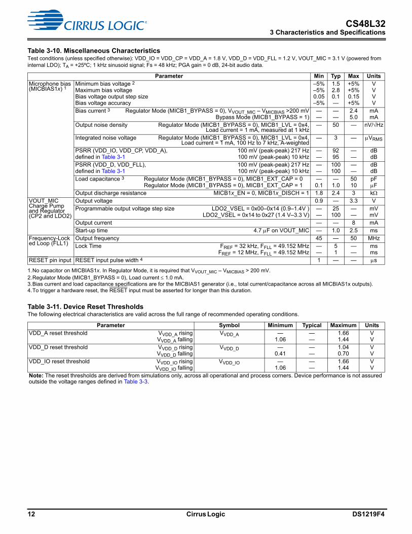
Table 3-10. Miscellaneous CharacteristicsTest conditions (unless specified otherwise): VDD_IO = VDD_CP = VDD_A = 1.8 V, VDD_D = VDD_FLL = 1.2 V, VOUT_MIC = 3.1 V (powered from internal LDO); TA = +25ºC; 1 kHz sinusoid signal; Fs = 48 kHz; PGA gain = 0 dB, 24-bit audio data.
Parameter Min Typ Max UnitsMicrophone bias (MICBIAS1x) 1
1.No capacitor on MICBIAS1x. In Regulator Mode, it is required that VVOUT_MIC – VMICBIAS > 200 mV.
Minimum bias voltage 2Maximum bias voltageBias voltage output step sizeBias voltage accuracy
2.Regulator Mode (MICB1_BYPASS = 0), Load current 1.0 mA.
–5%–5%0.05–5%
1.52.80.1—
+5%+5%0.15+5%
VVVV
Bias current 3
3.Bias current and load capacitance specifications are for the MICBIAS1 generator (i.e., total current/capacitance across all MICBIAS1x outputs).
Regulator Mode (MICB1_BYPASS = 0), VVOUT_MIC – VMICBIAS >200 mVBypass Mode (MICB1_BYPASS = 1)
——
——
2.45.0
mAmA
Output noise density Regulator Mode (MICB1_BYPASS = 0), MICB1_LVL = 0x4,Load current = 1 mA, measured at 1 kHz
— 50 — nV/Hz
Integrated noise voltage Regulator Mode (MICB1_BYPASS = 0), MICB1_LVL = 0x4,Load current = 1 mA, 100 Hz to 7 kHz, A-weighted
— 3 — VRMS
PSRR (VDD_IO, VDD_CP, VDD_A),defined in Table 3-1
100 mV (peak-peak) 217 Hz100 mV (peak-peak) 10 kHz
——
9295
——
dBdB
PSRR (VDD_D, VDD_FLL),defined in Table 3-1
100 mV (peak-peak) 217 Hz100 mV (peak-peak) 10 kHz
——
100100
——
dBdB
Load capacitance 3 Regulator Mode (MICB1_BYPASS = 0), MICB1_EXT_CAP = 0Regulator Mode (MICB1_BYPASS = 0), MICB1_EXT_CAP = 1
—0.1
—1.0
5010
pFF
Output discharge resistance MICB1x_EN = 0, MICB1x_DISCH = 1 1.8 2.4 3 kVOUT_MIC Charge Pump and Regulator (CP2 and LDO2)
Output voltage 0.9 — 3.3 VProgrammable output voltage step size LDO2_VSEL = 0x00–0x14 (0.9–1.4V )
LDO2_VSEL = 0x14 to 0x27 (1.4 V–3.3 V)——
25100
——
mVmV
Output current — — 8 mAStart-up time 4.7 F on VOUT_MIC — 1.0 2.5 ms
Frequency-Locked Loop (FLL1)
Output frequency 45 — 50 MHzLock Time FREF = 32 kHz, FFLL = 49.152 MHz
FREF = 12 MHz, FFLL = 49.152 MHz——
51
——
msms
RESET pin input RESET input pulse width 4
4.To trigger a hardware reset, the RESET input must be asserted for longer than this duration.
1 — — s
Table 3-11. Device Reset ThresholdsThe following electrical characteristics are valid across the full range of recommended operating conditions.
Parameter Symbol Minimum Typical Maximum UnitsVDD_A reset threshold VVDD_A rising
VVDD_A fallingVVDD_A —
1.06——
1.661.44
VV
VDD_D reset threshold VVDD_D risingVVDD_D falling
VVDD_D —0.41
——
1.040.70
VV
VDD_IO reset threshold VVDD_IO risingVVDD_IO falling
VVDD_IO —1.06
——
1.661.44
VV
Note: The reset thresholds are derived from simulations only, across all operational and process corners. Device performance is not assured outside the voltage ranges defined in Table 3-3.
12 Cirrus Logic DS1219F4

CS48L323 Characteristics and Specifications
Table 3-12. System Clock and Frequency-Locked Loop (FLL)The following timing information is valid across the full range of recommended operating conditions.
Parameter Minimum Typical Maximum UnitsMaster clock timing (MCLK1) 1
1.If MCLK1 is selected as a source for SYSCLK (either directly or via the FLL), the frequency must be within 1% of the SYSCLK_FREQ setting.
MCLK cycle time MCLK as input to FLL, FLL1_REFCLK_DIV = 00MCLK as input to FLL, FLL1_REFCLK_DIV = 01MCLK as input to FLL, FLL1_REFCLK_DIV = 10MCLK as input to FLL, FLL1_REFCLK_DIV = 11
MCLK as direct SYSCLK source
773819
12.520
—————
—————
nsnsnsnsns
MCLK duty cycle MCLK as input to FLLMCLK as direct SYSCLK source
80:2060:40
——
20:8040:60
%%
Frequency-locked loop (FLL1)
FLL input frequency FLL1_REFCLK_DIV = 00FLL1_REFCLK_DIV = 01FLL1_REFCLK_DIV = 10FLL1_REFCLK_DIV = 11
0.0320.0640.1280.256
————
13265280
MHzMHzMHzMHz
Internal clocking SYSCLK frequency SYSCLK_FREQ = 000, SYSCLK_FRAC = 0SYSCLK_FREQ = 000, SYSCLK_FRAC = 1SYSCLK_FREQ = 001, SYSCLK_FRAC = 0SYSCLK_FREQ = 001, SYSCLK_FRAC = 1SYSCLK_FREQ = 010, SYSCLK_FRAC = 0SYSCLK_FREQ = 010, SYSCLK_FRAC = 1SYSCLK_FREQ = 011, SYSCLK_FRAC = 0SYSCLK_FREQ = 011, SYSCLK_FRAC = 1SYSCLK_FREQ = 100, SYSCLK_FRAC = 0SYSCLK_FREQ = 100, SYSCLK_FRAC = 1
–1%–1%–1%–1%–1%–1%–1%–1%–1%–1%
6.1445.644812.28811.289624.576
22.579249.152
45.158498.304
90.3168
+1%+1%+1%+1%+1%+1%+1%+1%+1%+1%
MHzMHzMHzMHzMHzMHzMHzMHzMHzMHz
Table 3-13. Digital Input (PDM/DMIC) Interface TimingThe following timing information is valid across the full range of recommended operating conditions.
Parameter 1
1.PDM/DMIC interface timing
Symbol Minimum Typical Maximum UnitsINn_PDMCLK cycle time tCY 160 163 1432 nsINn_PDMCLK duty cycle — 45 — 55 %INn_PDMCLK rise/fall time (25 pF load, 1.8 V supply) tr, tf 5 — 30 nsINn_PDMDATA (left) setup time to falling PDMCLK edge tLSU 15 — — nsINn_PDMDATA (left) hold time from falling PDMCLK edge tLH 0 — — nsINn_PDMDATA (right) setup time to rising PDMCLK edge tRSU 15 — — nsINn_PDMDATA (right) hold time from rising PDMCLK edge tRH 0 — — nsNote: The voltage reference for the DMIC interfaces is selectable, using the INn_PDM_SUP fields—each interface may be referenced to VOUT_MIC or MICBIAS1.
(left data)(right data )INn_PDMDATA
(input) VIL
VIH
tRHtRSU tLHtLSU
VL
INn_PDMCLK(output)
tCY
VH
tr tf
13 Cirrus Logic DS1219F4

CS48L323 Characteristics and Specifications
Table 3-14. AUX PDM Interface TimingThe following timing information is valid across the full range of recommended operating conditions.
Parameter 1
1.AUX PDM interface timing.
Symbol Minimum Typical Maximum UnitsMaster Mode AUXPDMn_CLK cycle time tCY 320 — 1432 ns
AUXPDMn_CLK duty cycle — 45 — 55 %AUXPDMn_CLK rise/fall time (25 pF load, VDD_IO = 1.8 V) tr, tf 5 — 30 nsAUXPDMn_DOUT valid from active CLK edge Analog input tDV — — 15 nsAUXPDMn_DOUT hold from active CLK edge Analog input tHO 0 — — nsAUXPDMn_DOUT propagation delay 2
2.DOUT propagation delay is measured from a rising/falling edge on INn_PDMDATA to the corresponding edge at AUXPDMn_DOUT.
Digital input tDD — — 18 nsAUXPDMn_CLK phase alignment 3
3.In Master Mode, CLK phase alignment represents the timing of the AUXPDMn_CLK signal with respect to the INn_PDMCLK.
Digital input tCD –5 — 5 nsSlave Mode AUXPDMn_CLK cycle time tCY 320 — 1432 ns
AUXPDMn_CLK duty cycle — 45 — 55 %AUXPDMn_DOUT valid from active CLK edge Analog input tDV — — 20 nsAUXPDMn_DOUT hold from active CLK edge Analog input tHO 0 — — nsAUXPDMn_DOUT propagation delay 2 Digital input tDD — — 18 nsAUXPDMn_CLK propagation delay 4
4.In Slave Mode, CLK propagation delay is measured from a rising/falling edge on AUXPDMn_CLK to the corresponding edge at INn_PDMCLK.
Digital input tCD — — 20 ns
(PDM data)AUXPDMn_DOUT
(output) VOL
VOH
VL
AUXPDMn_CLK(Master output/
Slave input)
tCY
VH
tr tftDV tHO
14 Cirrus Logic DS1219F4

CS48L323 Characteristics and Specifications
Table 3-15. Audio Serial Port—Master ModeTest conditions (unless specified otherwise): CLOAD = 25 pF (output pins); BCLK slew (10% to 90%) = 3.7–5.6 ns; with the exception of the conditions noted, the following electrical characteristics are valid across the full range of recommended operating conditions.
Parameter 1
1.Audio serial port timing—Master Mode. Note that BCLK and FSYNC outputs can be inverted if required; the figure shows the default, noninverted polarity.
Symbol Minimum Typical Maximum UnitsMaster Mode ASPn_BCLK cycle time tBCY 40 — — ns
ASPn_BCLK pulse width high tBCH 18 — — nsASPn_BCLK pulse width low tBCL 18 — — nsASPn_FSYNC propagation delay from BCLK falling edge 2
2.The timing of the ASPn_FSYNC signal is selectable. If the FSYNC advance option is enabled, the FSYNC transition is timed relative to the preceding BCLK edge. Under the required condition that BCLK is inverted in this case, the FSYNC transition is still timed relative to the falling BCLK edge.
tLRD 0 — 8.3 nsASPn_DOUT propagation delay from BCLK falling edge tDD 0 — 5 nsASPn_DIN setup time to BCLK rising edge tDSU 11 — — nsASPn_DIN hold time from BCLK rising edge tDH 0 — — ns
Master Mode, Slave FSYNC
ASPn_FSYNC setup time to BCLK rising edge tLRSU 14 — — nsASPn_FSYNC hold time from BCLK rising edge tLRH 0 — — ns
Notes: The descriptions above assume noninverted polarity of ASPn_BCLK.
BCLK(output)
FSYNC(output)
DOUT(output)
DIN(input)
tDD
tDHtDSU
tLRD
tBCH tBCL
tBCY
15 Cirrus Logic DS1219F4

CS48L323 Characteristics and Specifications
Table 3-16. Audio Serial Port—Slave ModeThe following timing information is valid across the full range of recommended operating conditions, unless otherwise noted.
Parameter 1,2
1.Audio serial port timing—Slave Mode. Note that BCLK and FSYNC inputs can be inverted if required; the figure shows the default, noninverted polarity.
2.If ASPn_BCLK or ASPn_FSYNC is selected as a source for SYSCLK (either directly or via the FLL), the frequency must be within 1% of the SYSCLK_FREQ setting.
Symbol Min Typ Max UnitsASPn_BCLK cycle time tBCY 40 — — nsASPn_BCLK pulse width high BCLK as direct SYSCLK source
All other conditionstBCHtBCH
1614
——
——
nsns
ASPn_BCLK pulse width low BCLK as direct SYSCLK sourceAll other conditions
tBCLtBCL
1614
——
——
nsns
CLOAD = 15 pF (output pins),BCLK slew (10%–90%) = 3 ns
ASPn_FSYNC set-up time to BCLK rising edge tLRSU 7 — — nsASPn_FSYNC hold time from BCLK rising edge tLRH 0 — — nsASPn_DOUT propagation delay from BCLK falling edge tDD 0 — 13.6 nsASPn_DIN set-up time to BCLK rising edge tDSU 2 — nsASPn_DIN hold time from BCLK rising edge tDH 0 — nsMaster FSYNC, ASPn_FSYNC propagation delay from BCLK falling edge tLRD — — 12.2 ns
CLOAD = 25 pF (output pins),BCLK slew (10%–90%) = 6 ns
ASPn_FSYNC set-up time to BCLK rising edge tLRSU 7 — nsASPn_FSYNC hold time from BCLK rising edge tLRH 0 — nsASPn_DOUT propagation delay from BCLK falling edge tDD 0 — 14.7 nsASPn_DIN set-up time to BCLK rising edge tDSU 2 — nsASPn_DIN hold time from BCLK rising edge tDH 0 — nsMaster FSYNC, ASPn_FSYNC propagation delay from BCLK falling edge tLRD — — 13.4 ns
Note: The descriptions above assume noninverted polarity of ASPn_BCLK.
BCLK(input)
FSYNC(input)
DOUT(output)
DIN(input)
tDSU
tDD
tDH
tLRH tLRSU
tBCH tBCL
tBCY
16 Cirrus Logic DS1219F4

CS48L323 Characteristics and Specifications
Table 3-17. Audio Serial Port Timing—TDM ModeThe following timing information is valid across the full range of recommended operating conditions, unless otherwise noted.
Parameter 1
1.Audio serial port timing—TDM Mode. The timing of the ASPn_DOUT tristating at the start and end of the data transmission is shown.
Min Typ Max UnitsMaster Mode—CLOAD (ASPn_DOUT) = 15 to 25 pF. BCLK slew (10%–90%) = 3.7ns to 5.6 ns.
ASPn_DOUT enable time from BCLK falling edge 0 — — nsASPn_DOUT disable time from BCLK falling edge — — 6 ns
Slave Mode—CLOAD (ASPn_DOUT) = 15 pF).BCLK slew (10%–90%) = 3 ns
ASPn_DOUT enable time from BCLK falling edge 2 — — nsASPn_DOUT disable time from BCLK falling edge — — 12.2 ns
Slave Mode—CLOAD (ASPn_DOUT) = 25 pF).BCLK slew (10%–90%) = 6 ns
ASPn_DOUT enable time from BCLK falling edge 2 — — nsASPn_DOUT disable time from BCLK falling edge — — 14.2 ns
Note: If TDM operation is used on the ASPn_DOUT pins, it is important that two devices do not attempt to drive the ASPn_DOUT pin simultaneously. To support this requirement, the ASPn_DOUT pins can be configured to be tristated when not outputting data.
BCLK
DOUT
ASPn_DOUT enable time ASPn_DOUT disable time
ASPn_DOUT undriven (tristate) ASPn_DOUT valid (codec output) ASPn_DOUT valid ASPn_DOUT undriven (tristate)
17 Cirrus Logic DS1219F4

CS48L323 Characteristics and Specifications
Table 3-18. Control Interface Timing (SPI1 Slave)The following timing information is valid across the full range of recommended operating conditions.
Parameter 1
1.Control interface timing
Symbol Min Typ Max Units
SS falling edge to SCK rising edge tSSU 2.6 — — ns
SCK falling edge to SS rising edge tSHO 0 — — ns
SCK pulse cycle time SYSCLK disabled (SYSCLK_EN = 0)SYSCLK_EN = 1, SYSCLK_FREQ = 000SYSCLK_EN = 1, SYSCLK_FREQ > 000
tSCYtSCYtSCY
2038.420
———
———
nsnsns
SCK pulse-width low tSCL 9 — — nsSCK pulse-width high tSCH 9 — — nsSCK falling edge to MISO transition MISO driven on SCK falling edge (SPI1_DPHA = 0)
SCK slew (90%–10%) = 5 ns, CLOAD (MISO) = 10 pFtDL 4 — 12 ns
SCK rising edge to MISO transition MISO driven on SCK rising edge (SPI1_DPHA = 1)SCK slew (10%–90%) = 5 ns, CLOAD (MISO) = 10 pF
tDL 4 — 10 ns
MOSI to SCK set-up time tDSU 1.5 — — nsMOSI to SCK hold time tDHO 1.7 — — ns
SS(input)
SCK(input)
tSSU tSHO
MOSI(input)
MISO output(driven on falling SCK edge)
tSCH tSCL
tSCY
tDL
tDHO
tDSU
MISO output(driven on rising SCK edge)
tDL
18 Cirrus Logic DS1219F4

CS48L323 Characteristics and Specifications
Table 3-19. Master Interface Timing (SPI2 Master)The following timing information is valid across the full range of recommended operating conditions.
Parameter 1
1.Master interface (SPI2) timing
Symbol Min Typ Max Units
SS falling edge to SCK rising edge tSSU 5 — — ns
SCK falling edge to SS rising edge tSHO 15.3 — — ns
SCK pulse cycle time tSCY 40 — — nsSCK pulse width low tSCL 19 — — nsSCK pulse width high tSCH 19 — — nsSIOn (input) to SCK set-up time tDSU 10.35 — — nsSIOn (input) to SCK hold time tDHO 0 — — nsSIOn (output) valid from falling SCK edge SCLK slew (90%–10%) = 5 ns, CLOAD (SIOn) = 25 pF tDV — — 18.3 nsSIOn (output) hold from falling SCK edge SCLK slew (90%–10%) = 5 ns, CLOAD (SIOn) = 25 pF tHO –3 — — ns
SS(output)
SCK(output)
tSSU tSHO
SIOn(output)
tSCH tSCL
tSCY
tDV tHO
SIOn(input)
tDHO
tDSU
19 Cirrus Logic DS1219F4

CS48L323 Characteristics and Specifications
Table 3-20. JTAG Interface TimingTest conditions (unless specified otherwise): CLOAD = 25 pF (output pins); TCK slew (20%–80%) = 5 ns; with the exception of the conditions noted, the following electrical characteristics are valid across the full range of recommended operating conditions.
Parameter 1
1.JTAG Interface timing
Symbol Minimum Typical Maximum UnitsTCK cycle time TCCY 50 — — nsTCK pulse width high TCCH 20 — — nsTCK pulse width low TCCL 20 — — nsTMS setup time to TCK rising edge TMSU 1 — — nsTMS hold time from TCK rising edge TMH 2 — — nsTDI setup time to TCK rising edge TDSU 1 — — nsTDI hold time from TCK rising edge TDH 2 — — nsTDO propagation delay from TCK falling edge TDD 0 — 17 nsTRST setup time to TCK rising edge TRSU 3 — — nsTRST hold time from TCK rising edge TRH 3 — — nsTRST pulse-width low — 20 — — ns
Table 3-21. Typical Signal LatencyTest conditions (unless specified otherwise):VDD_IO = VDD_CP = VDD_A = 1.8 V, VDD_D = VDD_FLL = 1.2 V; VOUT_MIC = Off (CP2 and LDO2 disabled); TA = +25ºC; Fs = 48 kHz; 24-bit audio data, I2S Slave Mode.
Operating Configuration Latency (s)ADC to ASP path—analog input (INn) to digital output (ASPn) 1
1.Digital core high-pass filter is included in the signal path.
192 kHz input, 192 kHz output, Synchronous96 kHz input, 96 kHz output, Synchronous48 kHz input, 48 kHz output, Synchronous
44.1 kHz input, 44.1 kHz output, Synchronous16 kHz input, 16 kHz output, Synchronous
8 kHz input, 8 kHz output, Synchronous8 kHz input, 48 kHz output, Isochronous 2
16 kHz input, 48 kHz output, Isochronous 2
2.Signal is routed via the ISRC function in the isochronous cases only.
5010019521556011701700865
TCK(input)
tCCH tCCL
tCCY
TDI(input)
tDSU tDH
TMS(input)
tMSU tMH
TDO(output)
tDD
TRST(input)
tRSU tRH
20 Cirrus Logic DS1219F4

CS48L324 Functional Description
4 Functional Description
The CS48L32 is a low-power audio hub incorporating a programmable DSP and a multichannel microphone interface. It provides flexible, high-performance audio interfacing for handheld devices in a small and cost-effective package.
4.1 Overview
The CS48L32 block diagram is shown in Fig. 4-1.
Figure 4-1. CS48L32 Block Diagram
The CS48L32 digital-mixing core supports a range of fixed-function and programmable DSP capabilities, ideally suited to low-power voice-trigger applications. Media enhancements such as dynamic range control (DRC) and multiband equalizer (EQ) are supported. The CS48L32 incorporates a Halo Core DSP, supporting the Cirrus Logic SoundClear™ suite of audio processing algorithms. The DSP is integrated within a fully flexible, all-digital mixing and routing engine with sample-rate converters, for wide use-case flexibility. Support for third-party DSP programming provides far-reaching opportunities for product differentiation.
The CS48L32 provides multiple digital audio interfaces—I2S and PDM—to provide independent isochronous connections to different processors (e.g., application processor, baseband processor, and wireless transceiver).
A flexible clocking arrangement supports a wide variety of external clock references, including clocking derived from the audio serial ports. The frequency-locked loop (FLL) circuit provides additional flexibility for system clocking, including low-power always-on operation. Seamless switching between clock sources is supported; free-running modes are also available.
Unused circuitry can be disabled under software control to save power; low leakage currents enable extended standby/off time in portable battery-powered applications. Versatile GPIO functionality is provided, including support for push-button inputs. Comprehensive interrupt functions, with status reporting, are also provided.
RESET
IRQ ASPn_BCLK Clocking Control
SYSCLK
GPIO
SPI1_SCKSPI1_SS
SPI1_MOSISPI1_MISO
Audio Serial PortsASP1, ASP2
AS
P1
_BC
LK
AS
P1
_F
SY
NC
AS
P1
_D
INA
SP
1_
DO
UT
AS
P2_
BC
LKA
SP
2_
FS
YN
CA
SP
2_
DIN
AS
P2
_D
OU
T
LDO and MICBIAS
Generators
MICBIAS1AMICBIAS1BMICBIAS1C
GND_CP
GND_SUB
VDD_FLLVDD_CP
VREF_FILT
VDD_AGND_A
VDD_IO
GND_D
VDD_D
Input Select
2 x ADC
2 x Stereo Digital Mic Interface
IN1LN_1/IN1_PDMCLKIN1LN_2
IN1LP_1/IN1_PDMDATAIN1LP_2
IN1RN_1/IN2_PDMCLKIN1RN_2
IN1RP_1/IN2_PDMDATAIN1RP_2
Control Interface
SPI
GP
IO2
GP
IO1
Reference Generator
PDM_CLK
Digital Mixing Core
Programmable DSPFive-band equalizer (EQ)
Dynamic range control (DRC)Low-pass/high-pass filter (LHPF)
Isochronous sample -rate conversionUltrasonic demodulatorPWM signal generator
CP_FLYNCP_FLYPCP_FILT
VOUT_MIC
Charge Pump
Auxiliary PDMAUXPDM1–2
AU
XP
DM
1_
CLK
AU
XP
DM
1_
DO
UT
AU
XP
DM
2_
CLK
AU
XP
DM
2_
DO
UT
MC
LK
1SPI2_SCKSPI2_SS
SPI2_SIO0SPI2_SIO1Quad-SPI
Master Interface
SPI2_SIO2SPI2_SIO3
CS48L32
21 Cirrus Logic DS1219F4

CS48L324.1 Overview
4.1.1 Digital Audio Core
The CS48L32 uses a core architecture based on all-digital signal routing, making digital audio effects available on all signal paths, regardless of whether the source data input is analog or digital. The digital mixing desk allows different audio effects to be applied simultaneously on many independent paths, while supporting a variety of sample rates. Soft mute and unmute control ensures smooth transitions between use cases without interrupting existing audio streams elsewhere.
The CS48L32 incorporates a Halo Core DSP, supporting programmable signal-processing algorithms. The DSP is optimized for audio applications, incorporating configurable FFT, FIR, LMS, and linear/dB-conversion accelerators. The DSP is supported by general-purpose timer and event-logger functions. A quad-SPI (QSPI) master interface enables high-speed data transfers between the DSP and external components such as flash-memory devices.
Highly flexible digital mixing, including mixing between audio interfaces, is possible. The CS48L32 performs multichannel full-duplex isochronous sample-rate conversion, providing use-case flexibility across a broad range of system architectures.
DRC functions are available for optimizing audio signal levels. In playback modes, the DRC can be used to maximize loudness, while limiting the signal level to avoid distortion, clipping, or battery droop, for high-power output drivers such as speaker amplifiers. In record modes, the DRC assists in applications where the signal level is unpredictable.
The five-band parametric EQ functions can be used to compensate for the frequency characteristics of the output transducers. EQ functions can be cascaded to provide additional frequency control. Programmable high-pass and low-pass filters are also available for general filtering applications, such as removal of wind and other low-frequency noise.
4.1.2 Analog and Digital Audio Interfaces
The CS48L32 supports up to four analog inputs or up to four digital inputs, multiplexed into two stereo input signal paths. The analog and digital microphone interfaces are powered from the integrated MICBIAS power-supply regulator. The input paths can be configured for low-power operation, ideal for analog or digital microphone input in always-on applications. Ultrasonic signal detection and demodulation functions are provided, supporting a variety of presence-detection applications.
The auxiliary PDM interface can be used to provide an audio path between microphones connected to the CS48L32 and a digital input to an external audio processor. The auxiliary PDM interface operates in master or slave modes.
Two audio serial ports (ASPs) each support PCM, TDM, and I2S data formats for compatibility with most industry-standard chipsets. ASP1 supports eight input/output channels; ASP2 supports four input/output channels. Bidirectional operation of 32-bit data at sample rates up to 192 kHz sample rates is supported.
4.1.3 Other Features
The CS48L32 incorporates a tone generator that can be used for beep functions through any of the audio signal paths. The tone generator provides two 1 kHz outputs, with configurable phase relationship, offering flexibility to create differential signals or test scenarios.
A white-noise generator is provided that can be routed within the digital core. The noise generator can provide comfort noise in cases where silence (digital mute) is not desirable.
Two pulse-width modulation (PWM) signal generators are incorporated. The duty cycle of each PWM signal can be modulated by an audio source or can be set to a fixed value using a control register setting. The PWM signal generators can be output directly on a GPIO pin.
The CS48L32 supports up to 16 GPIO pins, offering a range of input/output functions for interfacing, for detection of external hardware, and for providing logic outputs to other devices. The CS48L32 provides two dedicated GPIO pins; the remaining GPIOs are multiplexed with other pin-specific functions. Comprehensive interrupt functionality is also provided for monitoring internal and external event conditions.
22 Cirrus Logic DS1219F4

CS48L324.2 Input Signal Path
System clocking can be derived from the MCLK1 input pin. Alternatively, a digital audio interface operating in Slave Mode (ASP or PDM) can be used to provide a clock reference. The CS48L32 also provides an integrated FLL circuit for clock frequency conversion and stability. The flexible clocking architecture supports low-power always-on operation, with reference frequencies down to 32 kHz. Seamless switching between clock sources is supported; free-running FLL modes are also available.
The CS48L32 is configured using control registers, accessed via a slave SPI interface operating at up to 50 MHz. The simple analog architecture, combined with the integrated tone generator, enables straightforward device configuration and testing, minimizing debug time and reducing software effort.
The CS48L32 is powered from 1.2 V and 1.8 V external supplies. Integrated charge-pump and LDO-regulator circuits are used to generate supply rails for internal functions and to support powering or biasing of external microphones. Power consumption is optimized across a wide variety of voice and multimedia use cases.
4.2 Input Signal Path
The CS48L32 provides flexible input channels, supporting up to four analog inputs or up to four digital inputs. Selectable combinations of analog (mic or line) and digital inputs are multiplexed into two stereo input signal paths. Input path IN1 supports analog and digital inputs; input path IN2 supports digital inputs only.
The analog input paths support single-ended and differential configurations, programmable gain control, and are digitized using a high performance sigma-delta ADC. The analog input paths can be configured for low-power operation, ideal for always-on applications.
The digital input paths interface directly with external digital microphones; a separate microphone interface clock is supported for two stereo pairs of digital microphones. Digital outputs can be configured on the auxiliary PDM interfaces; these can be sourced from either the analog input or the digital PDM inputs.
The microphone bias (MICBIAS) generator provides a low-noise reference for biasing electret condenser microphones (ECMs) or for use as a low-noise supply for MEMS microphones and digital microphones. Switchable outputs from the MICBIAS generator allows three separate reference/supply outputs to be independently controlled.
Digital volume control is available on all inputs (analog and digital), with programmable ramp control for smooth, glitch-free operation. A configurable signal-detect function is available on each input signal path. Ultrasonic signal detection and demodulation functions are provided on the input signal paths, supporting a variety of presence-detection applications.
The input signal paths and control fields are shown in Fig. 4-2.
23 Cirrus Logic DS1219F4

CS48L324.2 Input Signal Path
Figure 4-2. Input Signal Paths
4.2.1 Analog Microphone Input
Up to four analog microphones can be connected to the CS48L32, either in single-ended or differential configuration. The input configuration and pin selection is controlled using the IN1x_SRC bits as described in Section 4.2.6.
For single-ended input, the microphone signal is connected to the noninverting input of the PGAs. The inverting inputs of the PGAs are connected to an internal reference in this configuration.
For differential input, the noninverted microphone signal is connected to the noninverting input of the PGAs and the inverted (or noisy ground) signal is connected to the inverting input pins.
The gain of the input PGAs is controlled via register settings, as defined in Section 4.2.6. Note that the input impedance of the analog input paths is fixed across all PGA gain settings.
The ECM analog input configurations are shown in Fig. 4-3 and Fig. 4-4. The integrated MICBIAS generator provides a low noise reference for biasing the ECMs.
+
-
ADC
+
-
ADC
DATA
CLK
IN1LN_1/IN1_PDMCLK
IN1LP_1/IN1_PDMDATA
IN1LP_2
IN1LN_2
IN1RN_1/IN2_PDMCLK
IN1RP_1/IN2_PDMDATA
IN1RP_2
IN1RN_2
DATA
CLK
IN1L
IN1R
Digital Mic Interface
IN2L
IN2R
Digital Mic Interface
IN1L_SRC[1:0] p. 30
IN1R_SRC[1:0] p. 31
IN2_OSR[2:0] p. 31IN2_PDM_SUP[1:0] p. 31
IN1L_PGA_VOL[6:0] p. 31IN1L_LP_MODE p. 30
IN1R_PGA_VOL[6:0] p. 31IN1R_LP_MODE p. 31
IN_VD_RAMP[2:0] p. 32IN_VI_RAMP[2:0] p. 32
IN1L_VOL[7:0] p. 32IN1L_MUTE p. 32IN1L_EN p. 28
IN1R_VOL[7:0] p. 32IN1R_MUTE p. 32IN1R_EN p. 28
IN2L_VOL[7:0] p. 32IN2L_MUTE p. 32IN2L_EN p. 28
IN2R_VOL[7:0] p. 32IN2R_MUTE p. 32IN2R_EN p. 28
IN_HPF_CUT[2:0] p. 31
IN1_MODE p. 30
IN1L_HPF p. 30
IN1R_HPF p. 31
IN2L_HPF p. 31
IN2R_HPF p. 31
IN1_OSR[2:0] p. 30IN1_PDM_SUP[1:0] p. 30
24 Cirrus Logic DS1219F4

CS48L324.2 Input Signal Path
Pseudodifferential connection is also possible—this is similar to the configuration shown in Fig. 4-4, but the GND connection is directly to the microphone (and IN1xN capacitor), instead of via a resistor. The typical connections for pseudodifferential input are shown in Fig. 4-5.
Analog MEMS microphones can be connected to the CS48L32 in a similar manner to the ECM configurations. Typical configurations are shown in Fig. 4-6 and Fig. 4-7. In this configuration, the integrated MICBIAS generator provides a low-noise power supply for the microphones.
Note: The VOUT_MIC pin can also be used (instead of MICBIAS) as a reference or power supply for external microphones. The MICBIAS outputs are recommended, because they offer better noise performance and independent enable/disable control.
Figure 4-3. Single-Ended ECM Input Figure 4-4. Differential ECM Input
Figure 4-5. Pseudodifferential ECM Input
Figure 4-6. Single-Ended MEMS Input Figure 4-7. Differential MEMS Input
To ADC
VREF
IN1LN, IN1RN
IN1LP, IN1RP
ECM
GND
MICBIAS
PGA+
–
To ADC
VREF
ECM
GND
MICBIAS
PGA+
–IN1LN, IN1RN
IN1LP, IN1RP
To ADC
VREF
ECM
GND
MICBIAS
PGA+
–IN1LN, IN1RN
IN1LP, IN1RP
To ADC
VREF
MEMS Mic
MICBIAS
VDD
OUT
GND
GND
PGA+
–IN1LN, IN1RN
IN1LP, IN1RP
To ADC
VREF
MEMS Mic
MICBIAS
VDD
OUT-P
GND
GND
OUT-N PGA+
–IN1LN, IN1RN
IN1LP, IN1RP
DS1219F4 Cirrus Logic 25

CS48L324.2 Input Signal Path
4.2.2 Analog Line Input
Line inputs can be connected to the CS48L32 in a similar manner to the mic inputs. Single-ended and differential configurations are supported on each analog input path, using the IN1x_SRC bits as described in Section 4.2.6.
The analog line input configurations are shown in Fig. 4-8 and Fig. 4-9. Note that the microphone bias (MICBIAS) is not used for line input connections.
4.2.3 PDM (DMIC) Input
The CS48L32 supports as many as four PDM input channels, ideal for use with digital microphone (DMIC) input and other digital interfaces. The IN1 input path supports analog and digital input; digital (PDM) operation is selected using IN1_MODE as described in Section 4.2.6.
In PDM mode, two channels of audio data are multiplexed on the associated INn_PDMDATA pin. Each stereo interface is clocked using the respective INn_PDMCLK pin.
If PDM input is enabled, the CS48L32 outputs the CLK signal on the applicable INn_PDMCLK pins. The CLK frequency is controlled by the respective INn_OSR field, as described in Table 4-1 and Table 4-3. Note that the input-path PDM interfaces operate in Master Mode only—the clock (CLK) signal is generated by the CS48L32.
Note that, if ultrasonic signal detection or demodulation is enabled (see Section 4.2.9), the CLK frequency for the respective input path must be 1.536 MHz or 3.072 MHz.
Note that, if the 384 kHz or 768 kHz CLK frequency is selected, the maximum valid sample rate for the respective paths is restricted as described in Table 4-1. If the input sample rates are set globally using IN_RATE (i.e., IN_RATE_MODE = 0), all input paths are affected similarly.
The system clock, SYSCLK, must be present and enabled if using the PDM inputs; see Section 4.8 for details of SYSCLK and the associated registers.
The PDM clock frequencies in Table 4-1 assume that the SYSCLK frequency is a multiple of 6.144 MHz (SYSCLK_FRAC = 0). If the SYSCLK frequency is a multiple of 5.6448 MHz (SYSCLK_FRAC = 1), the PDM clock frequencies are scaled accordingly.
Figure 4-8. Single-Ended Line Input Figure 4-9. Differential Line Input
Table 4-1. PDM Clock Frequency
Condition PDM Clock Frequency Valid Sample Rates Signal PassbandINn_OSR = 000 384 kHz Up to 48 kHz Up to 4 kHzINn_OSR = 001 768 kHz Up to 96 kHz Up to 8 kHzINn_OSR = 010 1.536 MHz Up to 192 kHz Up to 20 kHzINn_OSR = 011 2.048 MHz Up to 192 kHz Up to 20 kHzINn_OSR = 100 2.4576 MHz Up to 192 kHz Up to 20 kHzINn_OSR = 101 3.072 MHz Up to 192 kHz Up to 20 kHzINn_OSR = 110 6.144 MHz Up to 192 kHz Up to 96 kHz
GND
Line
To ADC
VREF
PGA+
–IN1LN, IN1RN
IN1LP, IN1RP
To ADC
VREF
Line
PGA+
–IN1LN, IN1RN
IN1LP, IN1RP
26 Cirrus Logic DS1219F4

CS48L324.2 Input Signal Path
The voltage reference for the PDM interfaces is selectable, using INn_PDM_SUP; each interface may be referenced to VOUT_MIC or MICBIAS1. For DMIC use cases, the voltage reference for each input path should be set equal to the power supply of the respective microphones.
A pair of digital microphones is connected as shown in Fig. 4-10. The microphones must be configured to ensure that the left mic transmits a data bit when INn_PDMCLK is high and the right mic transmits a data bit when INn_PDMCLK is low. The CS48L32 samples the DMIC data at the end of each INn_PDMCLK phase. Each microphone must tristate its data output while the other microphone is transmitting.
Note that the CS48L32 provides integrated pull-down resistors on the INn_PDMDATA pins. This provides a flexible capability for interfacing with other devices.
Figure 4-10. DMIC Input
Two PDM channels are interleaved on INn_PDMDATA, as shown in Fig. 4-11. If two microphones are connected to provide a stereo interface, each microphone must tristate its data output while the other microphone is transmitting.
Figure 4-11. PDM (DMIC) Interface Timing
Digital Mic
VOUT_MIC or MICBIAS1x
GND_A
Digital Mic
VDD CLK DATA VDD CLK DATA
CHANCHAN
VDD
INn_PDMDATA
INn_PDMCLKPDM (Digital Microphone )
Interface
The PDM inputs are referenced to VOUT_MIC or MICBIAS1.
The supply for each digital microphone should provide the same voltage as the applicable reference.GND GND
INn_PDMCLK clock
INn_PDMDATA pin(Left and right channels interleaved) 1 2 1 2 1 2
Left mic output 1 1 1
Right mic output 2 2 2
Hi-Z
DS1219F4 Cirrus Logic 27

CS48L324.2 Input Signal Path
4.2.4 Input Signal Path Enable
The input signal paths are enabled using the bits described in Table 4-2. The respective bits must be enabled for analog or digital input on the respective input paths.
If the IN1 signal path is configured for analog input (IN1_MODE = 0, see Section 4.2.6), the following control sequence must be observed when enabling IN1 (left) or IN1 (right) input signal path:
1. If enabling the IN1 (left) path, write 0x2 to register 0x4688
2. If enabling the IN1 (right) path, write 0x2 to register 0x468C
3. Enable the required signal paths using IN1L_EN and IN1R_EN
4. Wait 200 s
5. If enabling the IN1 (left) path, write 0x0 to register 0x4688
6. If enabling the IN1 (right) path, write 0x0 to register 0x468C
Notes: If enabling one channel, with the other channel already enabled, the control steps relating to the already-enabledchannel should be omitted.
The IN1L_EN and IN1R_EN bits must be cleared before changing IN1_MODE.
The input signal paths are muted by default. It is recommended that deselecting the mute should be the final step of the path-enable control sequence. Similarly, the mute should be selected as the first step of the path-disable control sequence. The input signal path mute functions are controlled using the bits described in Table 4-4.
The VOUT_MIC power domain must be enabled when using the analog input signal paths. This power domain is provided using an internal charge pump (CP2) and LDO regulator (LDO2). See Section 4.12 for details of these circuits.
The system clock, SYSCLK, must be configured and enabled before any audio path is enabled. See Section 4.8 for details of the system clocks.
The CS48L32 performs automatic checks to confirm that the SYSCLK frequency is high enough to support the input signal paths and associated ADCs. If the frequency is too low, an attempt to enable an input signal path fails. Note that active signal paths are not affected under such circumstances.
The status bits in register 0x4004 indicate the status of each input signal path. If an underclocked error condition occurs, these bits can be used to indicate which input signal paths have been enabled.
Table 4-2. Input Signal Path Enable
Register Address Bit Label Default DescriptionR16384 (0x4000)INPUT_CONTROL
3 IN2L_EN 0 Input Path 2 (left) enable0 = Disabled1 = Enabled
2 IN2R_EN 0 Input Path 2 (right) enable0 = Disabled1 = Enabled
1 IN1L_EN 0 Input Path 1 (left) enable0 = Disabled1 = Enabled
0 IN1R_EN 0 Input Path 1 (right) enable0 = Disabled1 = Enabled
28 Cirrus Logic DS1219F4

CS48L324.2 Input Signal Path
4.2.5 Input Signal Path Sample-Rate Control
The input signal paths may be selected as input to the digital mixers or signal-processing functions within the CS48L32 digital core. The sample rate for the input signal paths can be set globally, or can be configured independently for each input channel.
The IN_RATE_MODE bit (defined in Table 4-3) controls whether the input sample rates are set globally using IN_RATE, or independently for each input channel using the INnx_RATE fields (where n is 1–2 and x is L or R for the left/right channels respectively). The IN_RATE and INnx_RATE fields are defined in Table 4-21.
Note that sample-rate conversion is required when routing the input signal paths to any signal chain that is configured for a different sample rate.
4.2.6 Input Signal Path Configuration
The CS48L32 supports up to four analog inputs or up to four digital inputs. Selectable combinations of analog (mic or line) and digital inputs are multiplexed into two stereo input signal paths:
• Input path IN1 can be configured for single-ended, differential, or digital (PDM) operation. The analog input configuration and pin selection is controlled using the IN1x_SRC bits; digital input mode is selected by setting IN1_MODE.
• Input path IN2 supports digital inputs only, using the respective IN2_PDMCLK and IN2_PDMDATA pins.
Note: The external pin connections for IN2 are shared with the IN1R analog input paths. If IN2L or IN2R input paths are enabled, the IN1R analog input is restricted to differential (IN1RP_2–IN1RN_2) or single-ended (IN1RP_2) configurations only.
A configurable high-pass filter (HPF) is provided on the left and right channels of each input path. The applicable cut-off frequency is selected using IN_HPF_CUT. The filter can be enabled on each path independently using the INnx_HPF bits.
The analog input signal paths (single-ended or differential) each incorporate a PGA to provide gain in the range 0 dB to +31 dB in 1 dB steps. The analog input PGA gain is controlled using IN1L_PGA_VOL and IN1R_PGA_VOL. Note that the PGAs do not provide pop suppression; it is recommended that the gain should not be adjusted if the respective signal path is enabled.
If digital input mode is selected, the respective PDM clock (INn_PDMCLK) is generated by the CS48L32. The frequency is controlled by INn_OSR.
If a signal path is configured for digital input, the voltage reference for the associated input/output pins is selectable using INn_PDM_SUP—each interface may be referenced to VOUT_MIC or MICBIAS1. For DMIC use cases, the voltage reference for each input path should be set equal to the power supply of the respective microphones.
Note: When writing to IN1_MODE, INn_OSR, or INn_PDM_SUP, take care not to change other nonzero bits that are configured at the same register address. Bit [5] should be set at all times.
R16388 (0x4004)INPUT_STATUS
3 IN2L_STS 0 Input Path 2 (left) enable status0 = Disabled1 = Enabled
2 IN2R_STS 0 Input Path 2 (right) enable status0 = Disabled1 = Enabled
1 IN1L_STS 0 Input Path 1 (left) enable status0 = Disabled1 = Enabled
0 IN1R_STS 0 Input Path 1 (right) enable status0 = Disabled1 = Enabled
Table 4-2. Input Signal Path Enable (Cont.)
Register Address Bit Label Default Description
DS1219F4 Cirrus Logic 29
CS48L324.2 Input Signal Path
The CS48L32 input paths can be configured for power-saving operation, ideal for always-on applications. The low-power configurations allow the power consumption to be optimized with respect to the required audio performance characteristics.
• If a signal path is configured for analog input, low-power operation can be selected by setting the respective IN1x_LP_MODE bit.
The analog input path can be configured for mid-power operation by setting INn_OSR = 010. The IN1x_LP_MODE bit should be cleared in the mid-power configuration. The maximum input-signal level is reduced by 6 dB if mid-power operation is selected (see Table 3-4); the minimum PGA gain is 6 dB. The mid-power configuration is deselected by setting INn_OSR = 101.
• If a signal path is configured for digital input, the respective INn_PDMCLK frequency is configured using the INn_OSR bits. Reducing the INn_PDMCLK frequency reduces power consumption at the expense of audio performance. The INn_OSR field also supports high performance PDM mode whenever 6.144 MHz INn_PDMCLK is selected.
If 384 kHz or 768 kHz CLK frequency is selected, the maximum sample rate for the respective paths is restricted as described in Table 4-1. If the input sample rates are set globally using IN_RATE (i.e., IN_RATE_MODE = 0), all input paths are affected similarly.
The VOUT_MIC voltage is generated by an internal charge pump and LDO regulator. The MICBIAS1x outputs are derived from VOUT_MIC; see Section 4.12.
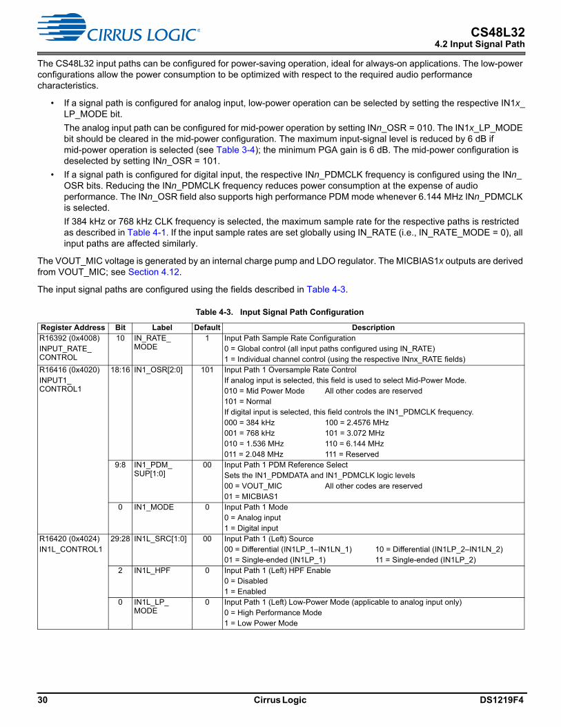
The input signal paths are configured using the fields described in Table 4-3.
Table 4-3. Input Signal Path Configuration
Register Address Bit Label Default DescriptionR16392 (0x4008)INPUT_RATE_CONTROL
10 IN_RATE_MODE
1 Input Path Sample Rate Configuration0 = Global control (all input paths configured using IN_RATE)1 = Individual channel control (using the respective INnx_RATE fields)
R16416 (0x4020)INPUT1_CONTROL1
18:16 IN1_OSR[2:0] 101 Input Path 1 Oversample Rate ControlIf analog input is selected, this field is used to select Mid-Power Mode.010 = Mid Power Mode101 = Normal
All other codes are reserved
If digital input is selected, this field controls the IN1_PDMCLK frequency.000 = 384 kHz001 = 768 kHz010 = 1.536 MHz011 = 2.048 MHz
100 = 2.4576 MHz101 = 3.072 MHz110 = 6.144 MHz111 = Reserved
9:8 IN1_PDM_SUP[1:0]
00 Input Path 1 PDM Reference SelectSets the IN1_PDMDATA and IN1_PDMCLK logic levels00 = VOUT_MIC01 = MICBIAS1
All other codes are reserved
0 IN1_MODE 0 Input Path 1 Mode0 = Analog input1 = Digital input
R16420 (0x4024)IN1L_CONTROL1
29:28 IN1L_SRC[1:0] 00 Input Path 1 (Left) Source00 = Differential (IN1LP_1–IN1LN_1)01 = Single-ended (IN1LP_1)
10 = Differential (IN1LP_2–IN1LN_2)11 = Single-ended (IN1LP_2)
2 IN1L_HPF 0 Input Path 1 (Left) HPF Enable0 = Disabled1 = Enabled
0 IN1L_LP_MODE
0 Input Path 1 (Left) Low-Power Mode (applicable to analog input only)0 = High Performance Mode1 = Low Power Mode
30 Cirrus Logic DS1219F4

CS48L324.2 Input Signal Path
4.2.7 Input Signal Path Digital Volume Control
A digital volume control is provided on each input signal path, providing –64 dB to +31.5 dB gain control in 0.5 dB steps. An independent mute control is also provided for each input signal path.
Updates to the digital-volume and mute functions are gated by the IN_VU bit: writing to the volume- or mute-control fields does not become effective until a 1 is written to IN_VU. This makes it possible to apply changes to multiple signal paths simultaneously.
Whenever the gain or mute setting is changed, the signal path gain is ramped up or down to the new settings at a programmable rate. For increasing gain (or unmute), the rate is controlled by IN_VI_RAMP. For decreasing gain (or mute), the rate is controlled by IN_VD_RAMP.
Note: The IN_VI_RAMP and IN_VD_RAMP fields should not be changed while a volume ramp is in progress.
Note that, although the digital-volume controls provide 0.5 dB steps, the internal circuits provide signal gain adjustment in 0.125 dB steps. This allows a very high degree of gain control and smooth volume ramping under all operating conditions.
R16424 (0x4028)IN1L_CONTROL2
7:1 IN1L_PGA_VOL[6:0]
0x40 Input Path 1 (Left) PGA Volume (applicable to analog input only)0x00 to 0x3F = Reserved0x40 = 0 dB0x41 = 1 dB
0x42 = 2 dB… (1 dB steps)0x5F = 31 dB
0x60 to 0x7F = Reserved
Note: In Mid-Power Mode, a minimum gain of 6 dB is used. Volume selections of 5 dB or less are overridden to 6 dB.
R16452 (0x4044)IN1R_CONTROL1
29:28 IN1R_SRC[1:0] 00 Input Path 1 (Right) Source00 = Differential (IN1RP_1–IN1RN_1)01 = Single-ended (IN1RP_1)
10 = Differential (IN1RP_2–IN1RN_2)11 = Single-ended (IN1RP_2)
2 IN1R_HPF 0 Input Path 1 (Right) HPF Enable0 = Disabled1 = Enabled
0 IN1R_LP_MODE
0 Input Path 1 (Right) Low-Power Mode (applicable to analog input only)0 = High Performance Mode1 = Low Power Mode
R16456 (0x4048)IN1R_CONTROL2
7:1 IN1R_PGA_VOL[6:0]
0x40 Input Path 1 (Right) PGA Volume (applicable to analog input only)0x00 to 0x3F = Reserved0x40 = 0 dB0x41 = 1 dB
0x42 = 2 dB… (1 dB steps)0x5F = 31 dB
0x60 to 0x7F = Reserved
Note: In Mid-Power Mode, a minimum gain of 6 dB is used. Volume selections of 5 dB or less are overridden to 6 dB.
R16480 (0x4060)INPUT2_CONTROL1
18:16 IN2_OSR[2:0] 101 Input Path 2 Oversample Rate Control - selects the IN2_PDMCLK frequency.000 = 384 kHz001 = 768 kHz010 = 1.536 MHz011 = 2.048 MHz
100 = 2.4576 MHz101 = 3.072 MHz110 = 6.144 MHz111 = Reserved
9:8 IN2_PDM_SUP[1:0]
00 Input Path 2 PDM Reference SelectSets the IN2_PDMDATA and IN2_PDMCLK logic levels00 = VOUT_MIC01 = MICBIAS1
All other codes are reserved
R16484 (0x4064)IN2L_CONTROL1
2 IN2L_HPF 0 Input Path 2 (Left) HPF Enable0 = Disabled1 = Enabled
R16516 (0x4084)IN2R_CONTROL1
2 IN2R_HPF 0 Input Path 2 (Right) HPF Enable0 = Disabled1 = Enabled
R16964 (0x4244)INPUT_HPF_CONTROL
2:0 IN_HPF_CUT[2:0]
010 Input Path IN1–IN2 HPF selectControls the cut-off frequency of the input path HPF circuits.000 = 2.5 Hz001 = 5 Hz
010 = 10 Hz011 = 20 Hz
100 = 40 HzAll other codes are reserved
Table 4-3. Input Signal Path Configuration (Cont.)
Register Address Bit Label Default Description
DS1219F4 Cirrus Logic 31

CS48L324.2 Input Signal Path
Note: The 0 dBFS level of the IN1–IN2 digital input paths is not equal to the 0 dBFS level of the CS48L32 digital core. The maximum digital input signal level is –6 dBFS (see Table 3-7). Under 0 dB gain conditions, a –6 dBFS input signal corresponds to a 0 dBFS input to the CS48L32 digital core functions.
The digital volume control registers are described in Table 4-4.
4.2.8 Input Signal Path Signal-Detect Control
The CS48L32 provides a digital signal-detect function for the input signal path. This enables system actions to be triggered by signal detection and allows the device to remain in a low-power state until a valid audio signal is detected. A mute function is integrated with the signal-detect circuit, ensuring the respective digital audio path remains at zero until the detection threshold level is reached. Signal detection is also indicated via the interrupt controller.
Table 4-4. Input Signal Path Digital Volume Control
Register Address Bit Label Default DescriptionR16404 (0x4014)INPUT_CONTROL3
29 IN_VU See Footnote 1
Input signal paths volume and mute update.Writing 1 to this bit causes the IN1–IN2 input signal paths volume and mute settings to be updated simultaneously.
R16424 (0x4028)IN1L_CONTROL2
28 IN1L_MUTE 1 Input Path 1 (Left) Digital Mute0 = Unmute1 = Mute
23:16 IN1L_VOL[7:0] 0x80 Input Path 1 (Left) Digital Volume, –64 dB to +31.5 dB in 0.5 dB steps0x00 = –64 dB0x01 = –63.5 dB… (0.5 dB steps)
0x80 = 0 dB… (0.5 dB steps)0xBF = +31.5 dB
0xC0 to 0xFF = Reserved
R16456 (0x4048)IN1R_CONTROL2
28 IN1R_MUTE 1 Input Path 1 (Right) Digital Mute0 = Unmute1 = Mute
23:16 IN1R_VOL[7:0] 0x80 Input Path 1 (Right) Digital Volume, –64 dB to +31.5 dB in 0.5 dB steps0x00 = –64 dB0x01 = –63.5 dB… (0.5 dB steps)
0x80 = 0 dB… (0.5 dB steps)0xBF = +31.5 dB
0xC0 to 0xFF = Reserved
R16488 (0x4068)IN2L_CONTROL2
28 IN2L_MUTE 1 Input Path 2 (Left) Digital Mute0 = Unmute1 = Mute
23:16 IN2L_VOL[7:0] 0x80 Input Path 2 (Left) Digital Volume, –64 dB to +31.5 dB in 0.5 dB steps0x00 = –64 dB0x01 = –63.5 dB… (0.5 dB steps)
0x80 = 0 dB… (0.5 dB steps)0xBF = +31.5 dB
0xC0 to 0xFF = Reserved
R16520 (0x4088)IN2R_CONTROL2
28 IN2R_MUTE 1 Input Path 2 (Right) Digital Mute0 = Unmute1 = Mute
23:16 IN2R_VOL[7:0] 0x80 Input Path 2 (Right) Digital Volume, –64 dB to +31.5 dB in 0.5 dB steps0x00 = –64 dB0x01 = –63.5 dB… (0.5 dB steps)
0x80 = 0 dB… (0.5 dB steps)0xBF = +31.5 dB
0xC0 to 0xFF = Reserved
R16968 (0x4248)INPUT_VOL_CONTROL
6:4 IN_VD_RAMP[2:0] 010 Input Volume Decreasing Ramp Rate (seconds/6 dB).This field should not be changed while a volume ramp is in progress.000 = 0 ms001 = 0.5 ms010 = 1 ms
011 = 2 ms100 = 4 ms101 = 8 ms
110 = 15 ms111 = 30 ms
2:0 IN_VI_RAMP[2:0] 010 Input Volume Increasing Ramp Rate (seconds/6 dB).This field should not be changed while a volume ramp is in progress.000 = 0 ms001 = 0.5 ms010 = 1 ms
011 = 2 ms100 = 4 ms101 = 8 ms
110 = 15 ms111 = 30 ms
1. Default is not applicable to these write-only bits
32 Cirrus Logic DS1219F4

CS48L324.2 Input Signal Path
The signal-detect function is supported on input paths IN1–IN2 in analog and digital configurations. (For the IN1 input path, digital input is selected by setting IN1_MODE.) Note that the valid operating conditions for this function vary, depending on the applicable signal-path configuration.
• The signal-detect function is supported on analog input paths for sample rates up to 16 kHz.
• The signal-detect function is supported on digital input paths for sample rates up to 16 kHz (if INn_PDMCLK 768kHz) and up to 48 kHz (if INn_PDMCLK 2.8224 MHz).
For each input path, the signal-detect function is enabled by setting the respective INnx_SIG_DET_EN bit. The detection threshold level is set using IN_SIG_DET_THR—this applies to all input paths.
If the signal-detect function is enabled, the respective input channel is muted if the signal level is below the configured threshold. If the input signal exceeds the threshold level, the respective channel is immediately unmuted.
If the input signal falls below the threshold level, the mute is applied. To prevent erroneous behavior, a time delay is applied before muting the input signal—the channel is only muted if the signal level remains below the threshold level for longer than the hold time. The hold time is set using IN_SIG_DET_HOLD.
Note that the signal-level detection is performed in the digital domain, after the ADC, PGA, digital mute and digital volume controls—the respective input channel must be enabled and unmuted when using the signal-detect function.
The signal-detect function is an input to the interrupt control circuit and can be used to trigger an interrupt event; see Section 4.9. Note that the respective interrupt event represents the logic OR of the signal detection on all input channels and does not provide indication of which input channel caused the interrupt. To avoid multiple interrupts, the signal-detect interrupt can be reasserted only after all input channels have fallen below the trigger threshold level.
The signal-detect status can be output directly on a GPIO pin as an external indication of the input path signal detection. See Section 4.10 to configure a GPIO pin for this function.
The input path signal-detection control registers are described in Table 4-5.
Table 4-5. Input Signal Path Signal-Detect Control
Register Address Bit Label Default DescriptionR16420 (0x4024)IN1L_CONTROL1
1 IN1L_SIG_DET_EN
0 Input Path 1 (Left) Signal-Detect Enable0 = Disabled1 = Enabled
R16452 (0x4044)IN1R_CONTROL1
1 IN1R_SIG_DET_EN
0 Input Path 1 (Right) Signal-Detect Enable0 = Disabled1 = Enabled
R16484 (0x4064)IN2L_CONTROL1
1 IN2L_SIG_DET_EN
0 Input Path 2 (Left) Signal-Detect Enable0 = Disabled1 = Enabled
R16516 (0x4084)IN2R_CONTROL1
1 IN2R_SIG_DET_EN
0 Input Path 2 (Right) Signal-Detect Enable0 = Disabled1 = Enabled
R16960 (0x4240)IN_SIG_DET_CONTROL
8:4 IN_SIG_DET_THR[4:0]
0x00 Input Signal Path Signal-Detect Threshold0x00 = –30.1 dB0x01 = –36.1 dB0x02 = –42.1 dB0x03 = –48.2 dB0x04 = –50.7 dB
0x05 = –54.2 dB0x06 = –56.7 dB0x07 = –60.2 dB0x08 = –66.2 dB0x09 = –68.7 dB
0x0A = –72.2 dB0x0B = –74.7 dB0x0C = –78.3 dB0x0D = –80.8 dBAll other codes are reserved
3:0 IN_SIG_DET_HOLD[3:0]
0001 Input Signal Path Signal-Detect Hold Time (delay before signal detect indication is deasserted)0000 = Reserved0001 = 4–8 ms0010 = 8–12 ms0011 = 12–16 ms
... (4 ms steps)1001 = 36–40 ms1010 = 40–44 ms1011 = 48–52 ms
1100 = 96–100 ms1101 = 192–196 ms1110 = 384–388 ms1111 = 768–772 ms
DS1219F4 Cirrus Logic 33
CS48L324.2 Input Signal Path
4.2.9 Ultrasonic Signal Detection and Demodulation
The CS48L32 provides ultrasonic signal-processing functions on the input signal paths. Configurable filters and demodulator functions enable ultrasonic signals to be translated down to the audio band and routed through the digital mixer core. Ultrasonic signal detection is also supported, with an interrupt event generated when the detection conditions are met. Two ultrasonic processing blocks are incorporated, with independent configuration controls for each.
The input source for the ultrasonic blocks is configured using the USn_SRC fields (where n identifies the applicable block US1 or US2). The input signal gain is set using USn_GAIN. The input frequency range is selected by USn_FREQ.
Note: The input path to the ultrasonic blocks incorporate a gain of –6 dB (in addition to the gain selected by USn_GAIN).
The selected input source for ultrasonic signal detection may be either analog or digital (see Section 4.2.6 to configure the input path for analog or digital input). The CLK frequency for the digital (PDM) input signal paths is configured using INn_OSR for the respective path (see Table 4-3); the CLK frequency must be 1.536 MHz or 3.072 MHz if ultrasonic signal detection or demodulation is enabled.
The ultrasonic functions can be supported on any of the input signal paths (IN1–IN2). The inputs to the ultrasonic functions are independent of the enable, high-pass filter, mute, and digital-volume settings of the respective input signal paths—these controls have no effect on the ultrasonic functions.
The system clock, SYSCLK, must be present and enabled when using the ultrasonic functions. The SYSCLK frequency must be a multiple of 6.144 MHz (SYSCLK_FRAC = 0) in this case. See Section 4.8 for details of SYSCLK and the associated registers.
The signal-detection function is enabled by setting USn_DET_EN. Note that signal detection can be supported without enabling the ultrasonic demodulator—ideal for low power signal-detection use cases.
The signal-detection algorithm uses an accumulator to count the instances where the input signal exceeds a detection threshold level—the count increases on each valid detection. If the input signal is below the threshold, a delay (hold time) is applied before decreasing the accumulator value. If the accumulator reaches the signal-detect level, an interrupt event is generated to indicate the successful detection. If no valid detection is made for the duration of the hold time, the accumulator value decreases at an exponential rate characterized by a configurable decay time.
A low-pass filter is incorporated in the signal path of the ultrasonic-detection circuit; this can be used to remove unwanted signal content. The low-pass filter is enabled using USn_DET_LPF; the cut-off frequency is configured using USn_DET_LPF_CUT. Note that the filter characteristics vary with USn_FREQ, as described in Table 4-6.
The USn_DET_THR field configures the detection threshold level. The signal-detection rate is determined by the USn_FREQ setting as described in Table 4-6—this is the frequency at which the input signal is measured against the detection threshold level.
The USn_DET_NUM field sets the accumulator count threshold at which a valid detection is indicated. The accumulator hold duration is configured using USn_DET_HOLD. The accumulator decay time constant is configured using USn_DET_DCY. The hold and decay parameters are defined as a function of the signal-detection rate.
The ultrasonic signal-detection function is an input to the interrupt control circuit and can be used to trigger an interrupt event—see Section 4.9.
The ultrasonic signal-detect status can be output directly on a GPIO pin as an external indication of the signal detection. See Section 4.10 to configure a GPIO pin for this function.
34 Cirrus Logic DS1219F4

CS48L324.2 Input Signal Path
The signal-detection algorithm is illustrated in Fig. 4-12.
Figure 4-12. Ultrasonic Signal Detection
The ultrasonic demodulator function is enabled by setting USn_EN. The frequency band and signal gain are selected using USn_FREQ and USn_GAIN respectively.
The output from the ultrasonic demodulator is a frequency-modulated image of the selected input frequency range. The folding frequency that characterizes the frequency modulation is set according to the USn_FREQ setting—see Table 4-6. The relationship between input and output frequencies is described in Eq. 4-1.
Equation 4-1. Ultrasonic Demodulator Characteristic
Note that, depending on the input frequency range and the folding frequency, FFOLD, the modulated output in respect of certain input frequencies may overlap others. This effect arises if the folding frequency lies within the input frequency range, with the result that two different input frequencies will each be modulated to the same output frequency. This effect is limited to the outer edges of the input frequency range in all cases. Amplitude response across the input frequency range is flat to within 1.5 dB in all cases.
The demodulated ultrasonic outputs can be selected as input to the digital mixers or signal-processing functions within the digital core by setting the respective x_SRCn fields as described in Section 4.3.1.
The sample rate for the demodulated ultrasonic output is configured using USn_RATE—see Table 4-21. The selected sample rate must be one of the SYSCLK-related rates, and must be equal to the output rate set by USn_FREQ (see Table 4-6). Note that sample-rate conversion is required when routing the ultrasonic signals to any signal chain that is configured for a different sample rate.
The characteristics associated with the USn_FREQ field setting are shown in Table 4-6.
Table 4-6. Ultrasonic Frequency Control
Condition Input Frequency Band Output Sample RateDemodulator Folding
Frequency (FFOLD)Signal-Detection Rate
USn_FREQ = 010 16–24 kHz 16 kHz 16 kHz 80.8 kHzUSn_FREQ = 011 20–28 kHz 16 kHz 20.21 kHz 96 kHz
Threshold detect
Accumulator count
Signal detection
Accumulator value increases if threshold detection is valid
Accumulator value is unchanged during hold time
Accumulator value falls after hold time expires
Status indication when accumulator reaches signal-detect level. Interrupt on rising edge.
Signal level measurements
Hold TimeUSn_DET_HOLD
Signal-detect levelUSn_DET_NUM
Decay TimeUSn_DET_DCY
FOUT FIN FFOLD–=
DS1219F4 Cirrus Logic 35

CS48L324.2 Input Signal Path
The ultrasonic detection and demodulation control registers are described in Table 4-7.
Table 4-7. Ultrasonic Signal-Detect and Demodulation Control
Register Address Bit Label Default DescriptionR47104 (0xB800)US_CONTROL
9 US2_DET_EN 0 Ultrasonic Detect 2 Enable0 = Disabled1 = Enabled
8 US1_DET_EN 0 Ultrasonic Detect 1 Enable0 = Disabled1 = Enabled
1 US2_EN 0 Ultrasonic Demodulator 2 Enable0 = Disabled1 = Enabled
0 US1_EN 0 Ultrasonic Demodulator 1 Enable0 = Disabled1 = Enabled
R47108 (0xB804)US1_CONTROL
13:12 US1_GAIN[1:0] 10 Ultrasonic Demodulator 1 Gain00 = Disabled (no signal)01 = –5 dB
10 = 1 dB11 = 7 dB
11:8 US1_SRC[3:0] 0x0 Ultrasonic Demodulator 1 Source0x0 = IN1L0x1 = IN1R0x2 = IN2L0x3 = IN2R
All other codes are reserved
6:4 US1_FREQ[2:0] 011 Ultrasonic Demodulator 1 Frequency010 = 16–24 kHz011 = 20–28 kHz
All other codes are reserved
36 Cirrus Logic DS1219F4

CS48L324.2 Input Signal Path
R47112 (0xB808)US1_DET_CONTROL
30:28 US1_DET_DCY[2:0] 000 Ultrasonic Detect 1 Decay Time ConstantTime period (after the hold time, and in the absence of valid detections) for the accumulated count to decrease to 37% of its previous value.The quoted times are valid for US1_FREQ = 010; if US1_FREQ = 011, the time period is multiplied by 0.84.000 = 0 ms001 = 0.79 ms010 = 1.58 ms
011 = 3.16 ms100 = 6.33 ms101 = 12.67 ms
110 = 25.34 ms111 = 50.69 ms
27:24 US1_DET_HOLD[3:0] 0000 Ultrasonic Detect 1 Hold TimeThe number of invalid detections required before the accumulated count decreases is 2(X+4) – 1, where X is US1_DET_HOLD in integer coding and X > 0. If US1_DET_HOLD = 0, the hold time is 0. The detection frequency is set by US1_FREQ.0000 = 00001 = 310010 = 63
0011 = 127...1101 = 131071
1110 = 2621431111 = 524287
23:20 US1_DET_NUM[3:0] 0000 Ultrasonic Detect 1 Accumulator Count ThresholdAccumulated number of detections threshold is 2X, where X is US1_DET_NUM in integer coding. The detection frequency is set by US1_FREQ.0000 = 10001 = 20010 = 4
0011 = 8...1101 = 8192
1110 = 163841111 = 32768
18:16 US1_DET_THR[2:0 000 Ultrasonic Detect 1 Signal Level Threshold000 = –6 dBFS001 = –9 dBFS010 = –12 dBFS
011 = –15 dBFS100 = –18 dBFS101 = –21 dBFS
110 = –24 dBFS111 = –27 dBFS
6:5 US1_DET_LPF_CUT[1:0]
00 Ultrasonic Detect 1 Low-pass Filter ControlSelects the cut-off frequency of the low-pass filter, dependent on US1_FREQ.If US1_FREQ = 010 the low-pass filter is set as follows:00 = 1722 Hz, 01 = 833 Hz, 10 = 408 Hz, 11 = 203 HzIf US1_FREQ = 011 the low-pass filter is set as follows:00 = 2044 Hz, 01 = 989 Hz, 10 = 484 Hz, 11 = 241 Hz
4 US1_DET_LPF 0 Ultrasonic Detect 1 Low-pass Filter Enable0 = Disabled1 = Enabled
R47124 (0xB814)US2_CONTROL
13:12 US2_GAIN[1:0] 10 Ultrasonic Demodulator 2 Gain00 = Disabled (no signal)01 = –5 dB
10 = 1 dB11 = 7 dB
11:8 US2_SRC[3:0] 0x0 Ultrasonic Demodulator 2 Source0x0 = IN1L0x1 = IN1R0x2 = IN2L0x3 = IN2R
All other codes are reserved
6:4 US2_FREQ[2:0] 011 Ultrasonic Demodulator 2 Frequency010 = 16–24 kHz011 = 20–28 kHz
All other codes are reserved
Table 4-7. Ultrasonic Signal-Detect and Demodulation Control (Cont.)
Register Address Bit Label Default Description
DS1219F4 Cirrus Logic 37

CS48L324.2 Input Signal Path
4.2.10 Auxiliary PDM Interface
The CS48L32 provides two auxiliary PDM (AUXPDM) interfaces; each interface supports a digital output derived from one of the analog input paths. This can be used to provide an audio path between a microphone connected to the CS48L32 and a digital input to an external audio processor.
If an analog input source is selected, the AUXPDM provides a one-channel PDM conversion path. If a digital input source is selected, the CS48L32 passes the respective INn_PDMDATA signal directly to the AUXPDM data output pin—the interface can pass either mono or stereo data in this case.
R47128 (0xB818)US2_DET_CONTROL
14:12 US2_DET_DCY[2:0] 000 Ultrasonic Detect 2 Decay Time ConstantTime period (after the hold time, and in the absence of valid detections) for the accumulated count to decrease to 37% of its previous value.The quoted times are valid for US2_FREQ = 010. If US2_FREQ = 011, the time period is multiplied by 0.84.000 = 0 ms001 = 0.79 ms010 = 1.58 ms
011 = 3.16 ms100 = 6.33 ms101 = 12.67 ms
110 = 25.34 ms111 = 50.69 ms
11:8 US2_DET_HOLD[3:0] 0000 Ultrasonic Detect 2 Hold TimeThe number of invalid detections required before the accumulated count decreases is 2(X+4) – 1, where X is US2_DET_HOLD in integer coding and X > 0. If US2_DET_HOLD = 0, the hold time is 0. The detection frequency is set by US2_FREQ.0000 = 00001 = 310010 = 63
0011 = 127...1101 = 131071
1110 = 2621431111 = 524287
7:4 US2_DET_NUM[3:0] 0000 Ultrasonic Detect 2 Accumulator Count ThresholdAccumulated number of detections threshold is 2X, where X is US2_DET_NUM in integer coding. The detection frequency is set by US2_FREQ.0000 = 10001 = 20010 = 4
0011 = 8...1101 = 8192
1110 = 163841111 = 32768
2:0 US2_DET_THR[2:0 000 Ultrasonic Detect 2 Signal Level Threshold000 = –6 dBFS001 = –9 dBFS010 = –12 dBFS
011 = –15 dBFS100 = –18 dBFS101 = –21 dBFS
110 = –24 dBFS111 = –27 dBFS
6:5 US2_DET_LPF_CUT[1:0]
00 Ultrasonic Detect 2 Low-pass Filter ControlSelects the cut-off frequency of the low-pass filter, dependent on US2_FREQ.If US2_FREQ = 010 the low-pass filter is set as follows:00 = 1722 Hz, 01 = 833 Hz, 10 = 408 Hz, 11 = 203 HzIf US2_FREQ = 011 the low-pass filter is set as follows:00 = 2044 Hz, 01 = 989 Hz, 10 = 484 Hz, 11 = 241 Hz
4 US2_DET_LPF 0 Ultrasonic Detect 2 Low-pass Filter Enable0 = Disabled1 = Enabled
Table 4-7. Ultrasonic Signal-Detect and Demodulation Control (Cont.)
Register Address Bit Label Default Description
38 Cirrus Logic DS1219F4

CS48L324.2 Input Signal Path
The AUXPDM interface signal paths are shown in Fig. 4-13.
Figure 4-13. Auxiliary PDM Interface
The AUXPDM interfaces can be configured in Master or Slave Mode using AUXPDMn_MSTR (where n identifies the applicable interface 1 or 2). In Master Mode, the clock (CLK) signal is generated by the CS48L32; in Slave Mode, the CLK signal is an input to the CS48L32.
The CLK frequency is selected using AUXPDMn_FREQ. For each setting of this field, the actual frequency depends on whether SYSCLK is configured for 48 kHz- or 44.1 kHz-related sample rates. See Section 4.8 for details of the system clocks. Note that the CLK frequency must be configured in master and slave modes, using the AUXPDMn_FREQ field.
In Slave Mode, the CS48L32 system clock (SYSCLK) must be synchronized to the PDM CLK input. The applicable CLK must be selected using PDM_FLLCLK_SRC (see Table 4-8) and configured as FLL reference clock using FLL1_REFCLK_SRC. See Section 4.8 to configure SYSCLK using FLL1 as a clock reference.
Note: If one of the AUXPDM interfaces is configured in Slave Mode, the system clock (SYSCLK) must be synchronized to the respective CLK input. To operate more than one of these interfaces in Slave Mode concurrently, the respective interfaces must all be synchronous (i.e., referenced to a common clock source).
+
-
ADC
+
-
ADC
DATA
CLK
IN1LN_1/IN1_PDMCLK
IN1LP_1/IN1_PDMDATA
IN1LP_2
IN1LN_2
IN1RN_1/IN2_PDMCLK
IN1RP_1/IN2_PDMDATA
IN1RP_2
IN1RN_2
DATA
CLK
Auxiliary PDM Interface 1
AUXPDM1_CLK
AUXPDM1_DOUT
Auxiliary PDM Interface 2
Digital Mic Interface
Digital Mic Interface
Input signal path
IN1L (analog)
IN1L (digital)
IN1R (digital)
IN1R (analog)
IN2L (digital)IN2R (digital)
AUXPDM2_CLK
AUXPDM2_DOUT
AUXPDM1_SRC[3:0] p. 41
AUXPDM2_SRC[3:0] p. 42
AUXPDM1_DOUT_SRC[3:0] p. 41
AUXPDM2_DOUT_SRC[3:0] p. 41
DS1219F4 Cirrus Logic 39

CS48L324.2 Input Signal Path
The input source for each AUXPDM interface is selected using AUXPDMn_SRC and AUXPDMn_DOUT_SRC.
• If analog input is selected (AUXPDMn_DOUT_SRC = 0x0), the respective input path and ADC are enabled automatically. Note that the mute and digital-volume settings of the IN1 path have no effect on the AUXPDM output.
The AUXPDM interface is enabled by setting AUXPDMn_EN. Note that the other AUXPDM control fields should be configured before enabling the interface; the AUXPDMn_EN bit should be set as the final step of the AUXPDM-enable sequence. The AUXPDMn_EN bit should be cleared before changing the interface configuration.
Note that, in Master Mode, the clock output is undriven (high-impedance) if the AUXPDM interface is disabled; the clock output is enabled by setting AUXPDMn_EN. Integrated pull-down resistors can be enabled on the clock pins as described in Section 4.2.11.
The output signal can be muted and unmuted using AUXPDMn_MUTE. The timing of the data (DOUT) signal can be controlled using AUXPDMn_TXEDGE—this selects whether DOUT changes on the rising or falling edge of CLK.
The auxiliary PDM interface timing is shown in Fig. 4-14 (assuming analog input is selected). In Master Mode, the clock and data outputs are driven synchronously by the CS48L32. In Slave Mode, the timing of the output data is controlled by the external clock input. See Table 3-14 for timing information.
Figure 4-14. Auxiliary PDM Interface Timing (Analog Input Source)
• If digital input is selected (AUXPDMn_DOUT_SRC = 0x1 or 0x2), the respective INn_PDMDATA signal is passed directly to the AUXPDM data output pin— note that the interface can pass either mono or stereo data in this case.
If IN1_PDMDATA is selected as source, IN1_MODE must be set and one or both of IN1L/IN1R must be enabled. If IN2_PDMDATA is selected as source, one or both of IN2L/IN2R must be enabled.
Note that the AUXPDM interface _EN, _MUTE, and TXEDGE control fields have no effect if digital input is selected.
The auxiliary PDM interface timing needs to be considered in combination with the DMIC/PDM input path timing, if digital input is selected as the AUXPDM source. The associated signals are subject to propagation delays between the DMIC/PDM interface and the AUXPDM interface, as described in Table 3-14.
— The AUXPDMn_DATA output is sourced directly from the INn_PDMDATA input.
— In AUXPDM Master Mode, the INn_PDMCLK and AUXPDMn_CLK outputs are generated from SYSCLK. In AUXPDM Slave Mode, the INn_PDMCLK output is sourced directly from the AUXPDMn_CLK input.
Aux PDM clock
Aux PDM data(AUXPDMn_TXEDGE = 0)
Aux PDM data(AUXPDMn_TXEDGE = 1)
40 Cirrus Logic DS1219F4

CS48L324.2 Input Signal Path
The auxiliary PDM interface control registers are described in Table 4-8.
Table 4-8. Auxiliary PDM Interface Control
Register Address Bit Label Default DescriptionR4188 (0x105C)AUXPDM_CTRL2
7:4 AUXPDM2_DOUT_SRC[3:0]
0x0 Auxiliary PDM 2 data source0x0 = Analog (mono, selected using AUXPDM2_SRC)0x1 = Digital (stereo, from IN1_PDMDATA)0x2 = Digital (stereo, from IN2_PDMDATA)All other codes are reserved
3:0 AUXPDM1_DOUT_SRC[3:0]
0x0 Auxiliary PDM 1 data source0x0 = Analog (mono, selected using AUXPDM1_SRC)0x1 = Digital (stereo, from IN1_PDMDATA)0x2 = Digital (stereo, from IN2_PDMDATA)All other codes are reserved
R16396 (0x400C)INPUT_CONTROL2
3:0 PDM_FLLCLK_SRC[3:0]
0x0 PDM_CLK source select for FLL input reference(Only valid if the respective interface is configured in Slave Mode)0x8 = AUXPDM1_CLK0x9 = AUXPDM2_CLKAll other codes are reserved
R17152 (0x4300)AUXPDM_CONTROL1
1 AUXPDM2_EN 0 Auxiliary PDM 2 enable0 = Disabled1 = Enabled
0 AUXPDM1_EN 0 Auxiliary PDM 1 enable0 = Disabled1 = Enabled
R17156 (0x4304)AUXPDM_CONTROL2
1 AUXPDM2_MUTE 0 Auxiliary PDM 2 mute0 = Unmute1 = Mute
0 AUXPDM1_MUTE 0 Auxiliary PDM 1 mute0 = Unmute1 = Mute
R17160 (0x4308)AUXPDM1_CONTROL1
17:16 AUXPDM1_FREQ[1:0] 01 Auxiliary PDM 1 CLK rate00 = 3.072 MHz (2.8824 MHz)01 = 2.048 MHz (1.8816 MHz)
10 = 1.536 MHz (1.4112 MHz)11 = 768 kHz (705.6 kHz)
The frequencies in brackets apply for 44.1 kHz–related sample rates only (i.e., if SYSCLK_FRAC = 1). The Auxiliary PDM interface must be disabled when updating this field.
11:8 AUXPDM1_SRC[3:0] 0x0 Auxiliary PDM 1 analog source0x0 = IN1L0x1 = IN1R
All other codes are reserved
Only valid if AUXPDM1_DOUT_SRC = 0x0. The Auxiliary PDM interface must be disabled when updating this field.
4 AUXPDM1_TXEDGE 0 Auxiliary PDM 1 timing0 = Output data is driven on rising edge of AUXPDM1_CLK1 = Output data is driven on falling edge of AUXPDM1_CLKThe Auxiliary PDM interface must be disabled when updating this field.
3 AUXPDM1_MSTR 1 Auxiliary PDM 1 Master Mode select0 = AUXPDM1_CLK Slave Mode (input)1 = AUXPDM1_CLK Master mode (output)The Auxiliary PDM interface must be disabled when updating this field.
DS1219F4 Cirrus Logic 41

CS48L324.2 Input Signal Path
4.2.11 PDM (DMIC) Pin Configuration
PDM operation on the IN1 input path is selected using IN1_MODE, as described in Table 4-3. If PDM input is selected, the respective analog input functions are disabled and the IN1_PDMCLK and IN1_PDMDATA pins are configured for digital input/output. The IN2 input path supports digital input only; if the IN2L or IN2 inputs paths are enabled, the IN2_PDMCLK and IN2_PDMDATA pins are configured for digital input/output.
The CS48L32 provides integrated pull-down resistors on the INn_PDMDATA pins. Integrated pull-down resistors are also provided on the AUXPDMn_CLK pins. This provides a flexible capability for interfacing with other devices. The pull resistors can be configured independently using the bits described in Table 4-9. Note that, if the PDM input paths are disabled, the pull resistors are disabled on the respective pins.
The output drive strength of AUXPDMn_CLK and AUXPDMn_DOUT is selectable using the respective _DRV_STR bits described in Table 4-9.
R17168 (0x4310)AUXPDM2_CONTROL1
17:16 AUXPDM2_FREQ[1:0] 01 Auxiliary PDM 2 CLK rate00 = 3.072 MHz (2.8824 MHz)01 = 2.048 MHz (1.8816 MHz)
10 = 1.536 MHz (1.4112 MHz)11 = 768 kHz (705.6 kHz)
The frequencies in brackets apply for 44.1 kHz–related sample rates only (i.e., if SYSCLK_FRAC = 1). The Auxiliary PDM interface must be disabled when updating this field.
11:8 AUXPDM2_SRC[3:0] 0x0 Auxiliary PDM 2 analog source0x0 = IN1L0x1 = IN1R
All other codes are reserved
Only valid if AUXPDM2_DOUT_SRC = 0x0. The Auxiliary PDM interface must be disabled when updating this field.
4 AUXPDM2_TXEDGE 0 Auxiliary PDM 2 timing0 = Output data is driven on rising edge of AUXPDM2_CLK1 = Output data is driven on falling edge of AUXPDM2_CLKThe Auxiliary PDM interface must be disabled when updating this field.
3 AUXPDM2_MSTR 1 Auxiliary PDM 2 Master Mode select0 = AUXPDM2_CLK Slave Mode (input)1 = AUXPDM2_CLK Master mode (output)The Auxiliary PDM interface must be disabled when updating this field.
Table 4-9. PDM (DMIC) Pin Control
Register Address Bit Label Default DescriptionR4148 (0x1034)DMIC_PAD_CTRL
5 IN2_PDMDATA_PD 0 IN2_PDMDATA pull-down control0 = Disabled, 1 = Enabled
4 IN1_PDMDATA_PD 0 IN1_PDMDATA pull-down control0 = Disabled, 1 = Enabled
R4164 (0x1044)AUXPDM_CTRL
18 AUXPDM2_CLK_PD 0 AUXPDM2_CLK pull-down control0 = Disabled, 1 = Enabled
16 AUXPDM1_CLK_PD 0 AUXPDM1_CLK pull-down control0 = Disabled, 1 = Enabled
3 AUXPDM2_CLK_DRV_STR 1 AUXPDM2_CLK output drive strength0 = 4 mA, 1 = 8 mA
2 AUXPDM2_DOUT_DRV_STR 1 AUXPDM2_DOUT output drive strength0 = 4 mA, 1 = 8 mA
1 AUXPDM1_CLK_DRV_STR 1 AUXPDM1_CLK output drive strength0 = 4 mA, 1 = 8 mA
0 AUXPDM1_DOUT_DRV_STR 1 AUXPDM1_DOUT output drive strength0 = 4 mA, 1 = 8 mA
Table 4-8. Auxiliary PDM Interface Control (Cont.)
Register Address Bit Label Default Description
42 Cirrus Logic DS1219F4

CS48L324.3 Digital Core
4.3 Digital Core
The CS48L32 digital core provides extensive mixing and processing capabilities for multiple signal paths. The configuration is highly flexible and supports virtually every conceivable input/output connection between the available processing blocks.
The digital core provides parametric equalization (EQ) functions, DRC, and low-/high-pass filters (LHPF).
The CS48L32 supports multiple signal paths through the digital core. Stereo full-duplex sample-rate conversion is provided to allow digital audio to be routed between input (ADC/PDM) paths and audio serial ports (ASP1–ASP2) operating at different sample rates.
The DSP functions are programmable, using application-specific control sequences. Note that the DSP configuration data is lost whenever the VDD_D power domain is removed; the DSP configuration data must be downloaded to the CS48L32 each time the device is powered up.
The CS48L32 incorporates a tone generator that can be used for beep functions through any of the audio signal paths. A white-noise generator is incorporated, to provide comfort noise in cases where silence (digital mute) is not desirable.
Two pulse-width modulation (PWM) signal generators are provided; the PWM waveforms can be modulated by an audio source within the digital core and can be output on a GPIO pin.
An overview of the digital-core mixing and signal-processing functions is provided in Fig. 4-15. The control registers associated with the digital-core signal paths are shown in Fig. 4-16 through Fig. 4-27. The full list of digital mixer control registers (0x8080–0x907C) is provided in Section 6. Generic register field definitions are provided in Table 4-10.
The digital audio core is predominantly a 24-bit architecture, but also provides support for 32-bit signal paths. Audio samples of up to 32 bits are supported by the ASP functions. The respective signal mixers provide full support for 32-bit data words. Note that all other signal paths and signal-processing blocks within the digital core are limited to 24-bit data length; data samples are truncated to 24-bit length if they are routed through any function that does not support 32-bit data words.
DS1219F4 Cirrus Logic 43

CS48L324.3 Digital Core
Figure 4-15. Digital Core
4.3.1 Digital-Core Mixers
The CS48L32 provides an extensive digital mixing capability. The digital-core mixing and signal-processing blocks are shown in Fig. 4-15. A four-input digital mixer is associated with many of these functions, as shown. The digital mixer circuit is identical in each instance, providing up to four selectable input sources, with independent volume control on each input.
The control registers associated with the digital-core signal paths are shown in Fig. 4-16–Fig. 4-27. The full list of digital mixer control registers (0x8080–0x907C) is provided in Section 6.
Further description of the associated control registers is provided throughout Section 4.3. Generic register field definitions are provided in Table 4-10.
The digital mixer input sources are selected using the associated x_SRCn fields; the volume control is implemented via the associated x_VOLn fields.
The ISRC input functions support selectable input sources, but do not incorporate any digital mixing. The respective input source (x_SRCn) fields are identical to those of the digital mixers.
+(GPIO pin)
PWM
PWM1
PWM2
Tone Generator 1Tone Generator
Tone Generator 2
Noise Generator
White Noise Generator
Ultrasonic 1 path
Ultrasonic 2 path
IN1L signal path
IN1R signal path
IN2L signal path
IN2R signal path
+EQn
EQ
EQ1
EQ2EQ3
EQ4
+LHPFn
LHPF
LHPF1
LHPF2
LHPF3
LHPF4
DRCnLeft
DRCnRight
DRC
DRC1DRC2
+
+
ISRC1 INT1
ISRC1 INT2
ISRC1 DEC1
ISRC1 DEC2
ISRC1 INT3
ISRC1 INT4
ISRC1 DEC3
ISRC1 DEC4
Isochronous Sample Rate
Converter (ISRC)
ISRC1
ISRCn DEC1
ISRCn DEC2
ISRC3
Isochronous Sample Rate
Converter (ISRC)
ISRC2
ISRCn INT2
ISRCn INT1
DSP1 Ch 1
DSP1 Ch 2
DSP1 Ch 3
DSP1 Ch 4
DSP1 Ch 5
DSP1 Ch 6
DSP1
DSP1 Ch 7
DSP1 Ch 8
+
DSP Core
+ASPn TX1 output
+ASPn TX2 output
ASPn RX1
ASP1 = 8 input, 8 outputASP2 = 4 input, 4 output
ASP2
ASP1
etc.
ASPn RX2
etc.
44 Cirrus Logic DS1219F4

CS48L324.3 Digital Core
The x_SRCn fields select the input sources for the respective mixer or signal-processing block. Note that the selected input sources must be configured for the same sample rate as the blocks to which they are connected. Sample-rate conversion functions are available to support flexible interconnectivity; see Section 4.3.12.
A status bit is associated with each configurable input source, indicating whether the signal path is enabled. If an underclocked error condition occurs, these bits can be used to indicate which signal paths have been enabled.
The generic register field definition for the digital mixers is provided in Table 4-10.
4.3.2 Digital-Core Inputs
The digital core comprises multiple input paths, as shown in Fig. 4-16. Any of these inputs may be selected as a source to the digital mixers or signal-processing functions within the CS48L32 digital core.
Note that the outputs from other blocks within the digital core may also be selected as input to the digital mixers or signal-processing functions within the CS48L32 digital core. Those input sources, which are not shown in Fig. 4-16, are described separately throughout Section 4.3.
The hexadecimal numbers in Fig. 4-16 indicate the corresponding x_SRCn setting for selection of that signal as an input to another digital-core function.
The sample rate for the input signal paths is configured by using the applicable IN_RATE, ASPn_RATE, or USn_RATE; see Table 4-21. Note that sample-rate conversion is required when routing the input signal paths to any signal chain that is configured for a different sample rate.
Table 4-10. Digital-Core Mixer Control Registers
Register Address Bit Label Default DescriptionR32896 (0x8080)toR39132 (0x907C)
15 x_STSn 0 [Digital Core function] input n status0 = Disabled1 = Enabled
7:1 x_VOLn 0x40 [Digital Core mixer] input n volume. (–32 dB to +16 dB in 1 dB steps)0x00 to 0x20 = –32 dB0x21 = –31 dB0x22 = –30 dB
... (1 dB steps)0x40 = 0 dB... (1 dB steps)
0x50 = +16 dB0x51 to 0x7F = +16 dB
8:0 x_SRCn 0x000 [Digital Core function] input n source select 0x000 = Silence (mute)0x004 = Tone generator 10x005 = Tone generator 20x00C = Noise generator0x010 = IN1L signal path0x011 = IN1R signal path0x012 = IN2L signal path0x013 = IN2R signal path0x020 = ASP1 RX10x021 = ASP1 RX20x022 = ASP1 RX30x023 = ASP1 RX40x024 = ASP1 RX50x025 = ASP1 RX60x026 = ASP1 RX70x027 = ASP1 RX80x030 = ASP2 RX10x031 = ASP2 RX20x032 = ASP2 RX30x033 = ASP2 RX4
0x098 = ISRC1 INT10x099 = ISRC1 INT20x09A = ISRC1 INT30x09B = ISRC1 INT40x09C = ISRC1 DEC10x09D = ISRC1 DEC20x09E = ISRC1 DEC30x09F = ISRC1 DEC40x0A0 = ISRC2 INT10x0A1 = ISRC2 INT20x0A4 = ISRC2 DEC10x0A5 = ISRC2 DEC20x0A8 = ISRC3 INT10x0A9 = ISRC3 INT20x0AC = ISRC3 DEC10x0AD = ISRC3 DEC20x0B8 = EQ10x0B9 = EQ20x0BA = EQ30x0BB = EQ4
0x0C0 = DRC1 Left0x0C1 = DRC1 Right0x0C2 = DRC2 Left0x0C3 = DRC2 Right0x0C8 = LHPF10x0C9 = LHPF20x0CA = LHPF30x0CB = LHPF40x0D8 = Ultrasonic 10x0D9 = Ultrasonic 20x100 = DSP1 channel 10x101 = DSP1 channel 20x102 = DSP1 channel 30x103 = DSP1 channel 40x104 = DSP1 channel 50x105 = DSP1 channel 60x106 = DSP1 channel 70x107 = DSP1 channel 8
DS1219F4 Cirrus Logic 45

CS48L324.3 Digital Core
Figure 4-16. Digital-Core Inputs
4.3.3 Digital-Core Output Mixers
The digital core supports two audio serial port (ASP) interfaces. The output paths associated with ASP1–ASP2 are shown in Fig. 4-17. A four-input mixer is associated with each output. The four input sources are selectable in each case, and independent volume control is provided for each path.
The ASP1–ASP2 output mixer control fields (see Fig. 4-17) are located at addresses 0x8200 through 0x833C.
The full list of digital mixer control registers (0x8080–0x907C) is provided in Section 6. Generic register field definitions are provided in Table 4-10.
The x_SRCn fields select the input sources for the respective mixers. Note that the selected input sources must be configured for the same sample rate as the mixer to which they are connected. Sample-rate conversion functions are available to support flexible interconnectivity; see Section 4.3.12.
The sample rate for the output signal paths is configured using the applicable ASPn_RATE; see Table 4-21. Note that sample-rate conversion is required when routing the output signal paths to any signal chain that is configured for a different sample rate.
The ASPn_RATE fields must not be changed if any of the respective x_SRCn fields is nonzero. The associated x_SRCn fields must be cleared before writing new values to ASPn_RATE. A minimum delay of 125 s must be allowed between clearing the x_SRCn fields and writing to the associated ASPn_RATE fields. See Table 4-21 for details.
The ASPn output mixers provide full support for 32-bit data words. Audio samples of up to 32 bits are supported by the ASP functions. Note that other signal paths and signal-processing blocks within the digital core are limited to 24-bit data length; data samples are truncated to 24-bit length if they are routed through any function that does not support 32-bit data words.
The CS48L32 performs automatic checks to confirm that the SYSCLK frequency is high enough to support the output mixer paths. If the frequency is too low, an attempt to enable an output mixer path fails. Note that active signal paths are not affected under such circumstances.
The status bits in registers 0x8080–0x907C indicate the status of each digital mixer. If an underclocked error condition occurs, these bits can be used to indicate which mixer paths have been enabled.
Silence (mute) (0x000)
IN1L signal path (0x010)IN1R signal path (0x011)IN2L signal path (0x012)IN2R signal path (0x013)
ASP1 RX1 (0x020)ASP1 RX2 (0x021)ASP1 RX3 (0x022)ASP1 RX4 (0x023)ASP1 RX5 (0x024)ASP1 RX6 (0x025)ASP1 RX7 (0x026)ASP1 RX8 (0x027)
ASP2 RX1 (0x030)ASP2 RX2 (0x031)ASP2 RX3 (0x032)ASP2 RX4 (0x033)
Ultrasonic 1 (0x0D8)Ultrasonic 2 (0x0D9)
46 Cirrus Logic DS1219F4

CS48L324.3 Digital Core
Figure 4-17. Digital-Core ASP Outputs
4.3.4 Five-Band Parametric Equalizer (EQ)
The digital core provides four EQ processing blocks as shown in Fig. 4-18. A four-input mixer is associated with each EQ. The four input sources are selectable in each case, and independent volume control is provided for each path. Each EQ block supports one output.
The EQ provides selective control of five frequency bands as follows:
• The low-frequency band (Band 1) filter can be configured as a peak filter or as a shelving filter. If configured as a shelving filter, it provides adjustable gain below the Band 1 cut-off frequency. As a peak filter, it provides adjustable gain within a defined frequency band that is centered on the Band 1 frequency.
• The midfrequency bands (Band 2–Band 4) filters are peak filters that provide adjustable gain around the respective center frequency.
• The high-frequency band (Band 5) filter is a shelving filter that provides adjustable gain above the Band 5 cut-off frequency.
ASP2TXn_SRC1
ASP2TXn_SRC3
ASP2TXn_SRC4
ASP2TXn_SRC2
ASP2 TXn+
…
…
…
…
ASP1TXn_SRC1
ASP1TXn_SRC3
ASP1TXn_SRC4
ASP1TXn_SRC2
ASP1 TXn+
…
…
…
…
ASP2TXnMIX_VOL2
ASP2TXnMIX_VOL3
ASP2TXnMIX_VOL4
ASP2TXnMIX_VOL1
ASP1TXnMIX_VOL2
ASP1TXnMIX_VOL3
ASP1TXnMIX_VOL4
ASP1TXnMIX_VOL1
CS48L32 supports eight ASP1 output mixers, i.e., n = 1–8
CS48L32 supports four ASP2 output mixers, i.e., n = 1–4
x_SRCn p. 45x_VOLn p. 45
DS1219F4 Cirrus Logic 47

CS48L324.3 Digital Core
Figure 4-18. Digital-Core EQ Blocks
The EQ1–EQ4 mixer control fields (see Fig. 4-18) are located at addresses 0x8B80 through 0x8BBC.
The full list of digital-mixer control registers (0x8080–0x907C) is provided in Section 6. Generic register field definitions are provided in Table 4-10.
The x_SRCn fields select the input sources for the respective EQ processing blocks. Note that the selected input sources must be configured for the same sample rate as the EQ to which they are connected. Sample-rate conversion functions are available to support flexible interconnectivity; see Section 4.3.12.
The hexadecimal numbers in Fig. 4-18 indicate the corresponding x_SRCn setting for selection of that signal as an input to another digital-core function.
The sample rate for the EQ function is configured using FX_RATE; see Table 4-21. Note that the EQ, DRC, and LHPF functions must be configured for the same sample rate. Sample-rate conversion is required when routing the EQ signal paths to any signal chain that is configured for a different sample rate.
The FX_RATE field must not be changed if any of the associated x_SRCn fields is nonzero. The associated x_SRCn fields must be cleared before writing a new value to FX_RATE. A minimum delay of 125 s must be allowed between clearing the x_SRCn fields and writing to FX_RATE. See Table 4-21 for details.
The cut-off or center frequencies for the five-band EQ are set by using the coefficients held in the registers identified in Table 4-11. These coefficients are derived using tools provided in Cirrus Logic’s WISCE™ evaluation-board control software; please contact your Cirrus Logic representative for details.
Table 4-11. EQ Coefficient Registers
EQ Register AddressesEQ1 0xA818–0xA850EQ2 0xA85C–0xA894EQ3 0xA8A0–0xA8D8EQ4 0xA8E4–0xA91C
EQnMIX_VOL2
EQnMIX_VOL3
EQnMIX_VOL4
EQnMIX_VOL1EQn_SRC1
EQn_SRC3
EQn_SRC4
EQn_SRC2
EQ1 (0x0B8)EQ2 (0x0B9)EQ3 (0x0BA)EQ4 (0x0BB)
Five-band Equalizer
+ EQ
…
…
…
…
CS48L32 supports four EQ blocks, i.e., n = 1–4
x_SRCn p. 45x_VOLn p. 45
48 Cirrus Logic DS1219F4

CS48L324.3 Digital Core
The control registers associated with the EQ functions are described in Table 4-12.
Table 4-12. EQ Enable and Gain Control
Register Address Bit Label Default DescriptionR43012 (0xA804)FX_STATUS
11:0 FX_STS[11:0] 0x00 LHPF, DRC, EQ Enable Status. Indicates the status of each respective signal-processing function. Each bit is coded as follows:0 = Disabled1 = Enabled[11] = EQ4[10] = EQ3[9] = EQ2[8] = EQ1
[7] = DRC2 (Right)[6] = DRC2 (Left)[5] = DRC1 (Right)[4] = DRC1 (Left)
[3] = LHPF4[2] = LHPF3[1] = LHPF2[0] = LHPF1
R43016 (0xA808)EQ_CONTROL1
3 EQ4_EN 0 EQ4 Enable0 = Disabled1 = Enabled
2 EQ3_EN 0 EQ3 Enable0 = Disabled1 = Enabled
1 EQ2_EN 0 EQ2 Enable0 = Disabled1 = Enabled
0 EQ1_EN 0 EQ1 Enable0 = Disabled1 = Enabled
R43020 (0xA80C)EQ_CONTROL2
3 EQ4_B1_MODE 0 EQ4 Band 1 Mode0 = Shelving filter1 = Peak filter
2 EQ3_B1_MODE 0 EQ3 Band 1 Mode0 = Shelving filter1 = Peak filter
1 EQ2_B1_MODE 0 EQ2 Band 1 Mode0 = Shelving filter1 = Peak filter
0 EQ1_B1_MODE 0 EQ1 Band 1 Mode 0 = Shelving filter1 = Peak filter
R43024 (0xA810)EQ1_GAIN1
28:24 EQ1_B4_GAIN[4:0] 0x0C EQ1 Band n Gain (–12 dB to +12 dB in 1 dB steps)20:16 EQ1_B3_GAIN[4:0] 0x0C 0x00 = –12 dB
0x01 = –11 dB... (1 dB steps)
0x0C = 0 dB... (1 dB steps)0x17 = 11 dB
0x18 = 12 dBAll other codes are reserved
12:8 EQ1_B2_GAIN[4:0] 0x0C4:0 EQ1_B1_GAIN[4:0] 0x0C
R43028 (0xA814)EQ1_GAIN2
4:0 EQ1_B5_GAIN[4:0] 0x0C
R43032 (0xA818)toR43088 (0xA850)
— EQ1_* — EQ1 Frequency Coefficients. Refer to WISCE evaluation board control software for the derivation of these field values.
R43092 (0xA854)EQ2_GAIN1
28:24 EQ2_B4_GAIN[4:0] 0x0C EQ2 Band n Gain (–12 dB to +12 dB in 1 dB steps)20:16 EQ2_B3_GAIN[4:0] 0x0C 0x00 = –12 dB
0x01 = –11 dB... (1 dB steps)
0x0C = 0 dB... (1 dB steps)0x17 = 11 dB
0x18 = 12 dBAll other codes are reserved
12:8 EQ2_B2_GAIN[4:0] 0x0C4:0 EQ2_B1_GAIN[4:0] 0x0C
R43096 (0xA858)EQ2_GAIN2
4:0 EQ2_B5_GAIN[4:0] 0x0C
R43100 (0xA85C)toR43156 (0xA89C)
— EQ2_* — EQ2 Frequency Coefficients. Refer to WISCE evaluation board control software for the derivation of these field values.
DS1219F4 Cirrus Logic 49

CS48L324.3 Digital Core
The CS48L32 automatically checks to confirm whether the SYSCLK frequency is high enough to support the commanded EQ and digital mixing functions. If an attempt is made to enable an EQ signal path, and there are insufficient SYSCLK cycles to support it, the attempt does not succeed. Note that any signal paths that are already active are not affected under such circumstances.
The FX_STS field in register 0xA804 indicates the status of each EQ, DRC, and LHPF signal path. If an underclocked error condition occurs, this field can be used to indicate which EQ, DRC, or LHPF signal paths have been enabled.
The status bits in registers 0x8080–0x907C indicate the status of each digital mixer. If an underclocked error condition occurs, these bits can be used to indicate which mixer paths have been enabled.
4.3.5 Dynamic Range Control (DRC)
The digital core provides two stereo DRC processing blocks, as shown in Fig. 4-19. A four-input mixer is associated with each DRC input channel. The input sources are selectable in each case, and independent volume control is provided for each path. The stereo DRC blocks support two outputs each.
The function of the DRC is to adjust the signal gain in conditions where the input amplitude is unknown or varies over a wide range, for example, when recording from microphones built into a handheld system or to restrict the dynamic range of an output signal path.
To improve intelligibility in the presence of loud impulsive noises, the DRC can apply compression and automatic level control to the signal path. It incorporates anticlip and quick-release features for handling transients.
The DRC also incorporates a noise-gate function that provides additional attenuation of very low-level input signals. This means that the signal path is quiet when no signal is present, giving an improvement in background noise level under these conditions.
A signal-detect function is provided within the DRC; this can be used to detect the presence of an audio signal and to trigger other events. The DRC provides inputs to the interrupt control circuit for this purpose.
R43160 (0xA898)EQ3_GAIN1
28:24 EQ3_B4_GAIN[4:0] 0x0C EQ3 Band n Gain (–12 dB to +12 dB in 1 dB steps)20:16 EQ3_B3_GAIN[4:0] 0x0C 0x00 = –12 dB
0x01 = –11 dB... (1 dB steps)
0x0C = 0 dB... (1 dB steps)0x17 = 11 dB
0x18 = 12 dBAll other codes are reserved
12:8 EQ3_B2_GAIN[4:0] 0x0C4:0 EQ3_B1_GAIN[4:0] 0x0C
R43164 (0xA89C)EQ3_GAIN2
4:0 EQ3_B5_GAIN[4:0] 0x0C
R43168 (0xA8A0)toR43224 (0xA8D8)
— EQ3_* — EQ3 Frequency Coefficients. Refer to WISCE evaluation board control software for the derivation of these field values.
R43228 (0xA8DC)EQ4_GAIN1
28:24 EQ4_B4_GAIN[4:0] 0x0C EQ4 Band n Gain (–12 dB to +12 dB in 1 dB steps)20:16 EQ4_B3_GAIN[4:0] 0x0C 0x00 = –12 dB
0x01 = –11 dB... (1 dB steps)
0x0C = 0 dB... (1 dB steps)0x17 = 11 dB
0x18 = 12 dBAll other codes are reserved
12:8 EQ4_B2_GAIN[4:0] 0x0C4:0 EQ4_B1_GAIN[4:0] 0x0C
R43232 (0xA8E0)EQ4_GAIN2
4:0 EQ4_B5_GAIN[4:0] 0x0C
R43236 (0xA8E4)toR43292 (0xA91C)
— EQ4_* — EQ4 Frequency Coefficients. Refer to WISCE evaluation board control software for the derivation of these field values.
Table 4-12. EQ Enable and Gain Control (Cont.)
Register Address Bit Label Default Description
50 Cirrus Logic DS1219F4

CS48L324.3 Digital Core
Figure 4-19. Dynamic Range Control (DRC) Block
The DRC1 and DRC2 mixer control fields (see Fig. 4-19) are located at addresses 0x8C00 through 0x8C3C.
The full list of digital mixer control registers (0x8080–0x907C) is provided in Section 6. Generic register field definitions are provided in Table 4-10.
The x_SRCn fields select the input sources for the respective DRC processing blocks. Note that the selected input sources must be configured for the same sample rate as the DRC to which they are connected. Sample-rate conversion functions are available to support flexible interconnectivity; see Section 4.3.12.
The hexadecimal numbers in Fig. 4-19 indicate the corresponding x_SRCn setting for selection of that signal as an input to another digital-core function.
The sample rate for the DRC function is configured using FX_RATE; see Table 4-21. Note that the EQ, DRC, and LHPF functions must all be configured for the same sample rate. Sample-rate conversion is required when routing the DRC signal paths to any signal chain that is configured for a different sample rate.
The FX_RATE field must not be changed if any of the associated x_SRCn fields is nonzero. The associated x_SRCn fields must be cleared before writing a new value to FX_RATE. A minimum delay of 125 s must be allowed between clearing the x_SRCn fields and writing to FX_RATE. See Table 4-21 for details.
The DRC functions are enabled using the control bits described in Table 4-13.
DRCnLMIX_VOL2
DRCnLMIX_VOL3
DRCnLMIX_VOL4
DRCnLMIX_VOL1DRCnLMIX_SRC1
DRCnLMIX_SRC3
DRCnLMIX_SRC4
DRCnLMIX_SRC2
DRC1 Left (0x0C0)DRC2 Left (0x0C2)Dynamic Range
Controller
DRCnRMIX_VOL2
DRCnRMIX_VOL3
DRCnRMIX_VOL4
DRCnRMIX_VOL1DRCnRMIX_SRC1
DRCnRMIX_SRC3
DRCnRMIX_SRC4
DRCnRMIX_SRC2
DRC1 Right (0x0C1)DRC2 Right (0x0C3)Dynamic Range
Controller
DRC
DRC
…
…
…
…
…
…
…
…
+
+
CS48L32 supports two stereo DRC blocks, i.e., n = 1 or 2
x_SRCn p. 45x_VOLn p. 45
DS1219F4 Cirrus Logic 51

CS48L324.3 Digital Core
The following description of the DRC is applicable to each DRC. The associated control fields are described in Table 4-15 and Table 4-16 for DRC1 and DRC2 respectively.
4.3.5.1 DRC Compression, Expansion, and Limiting
The DRC supports two different compression regions, separated by a knee at a specific input amplitude (shown as Knee 1 in Fig. 4-20). In the region above the knee, the compression slope DRCn_HI_COMP applies; in the region below the knee, the compression slope DRCn_LO_COMP applies. Note that n identifies the applicable DRC 1 or 2.
The DRC also supports a noise-gate region, where low-level input signals are heavily attenuated. This function can be enabled or disabled according to the application requirements. The DRC response in this region is defined by the expansion slope DRCn_NG_EXP.
For additional attenuation of signals in the noise-gate region, an additional knee can be defined (shown as Knee 2 in Fig. 4-20). If this knee is enabled, there is an infinitely steep drop-off in the DRC response pattern between the DRCn_LO_COMP and DRCn_NG_EXP regions.
The overall DRC compression characteristic in steady state (i.e., where the input amplitude is near constant) is shown in Fig. 4-20.
Figure 4-20. DRC Response Characteristic
Table 4-13. DRC Enable
Register Address Bit Label Default DescriptionR43776 (0xAB00)DRC1_CONTROL1
1 DRC1L_EN 0 DRC1 (left) enable0 = Disabled1 = Enabled
0 DRC1R_EN 0 DRC1 (right) enable0 = Disabled1 = Enabled
R43796 (0xAB14)DRC2_CONTROL1
1 DRC2L_EN 0 DRC2 (left) enable0 = Disabled1 = Enabled
0 DRC2R_EN 0 DRC2 (right) enable0 = Disabled1 = Enabled
DRCn_KNEE1_IP
(Y0)
0dB
DRCn Input Amplitude (dB)
DRCn Output Amplitude (dB)
DRCn_KNEE1_OPKnee 1
Knee 2
DRCn_KNEE2_IP
DRCn_KNEE2_OP
52 Cirrus Logic DS1219F4

CS48L324.3 Digital Core
The slope of the DRC response is determined by DRCn_HI_COMP and DRCn_LO_COMP. A slope of 1 indicates constant gain in this region. A slope less than 1 represents compression (i.e., a change in input amplitude produces only a smaller change in output amplitude). A slope of 0 indicates that the target output amplitude is the same across a range of input amplitudes; this is infinite compression.
If the noise gate is enabled, the DRC response in this region is determined by DRCn_NG_EXP. A slope of 1 indicates constant gain in this region. A slope greater than 1 represents expansion (i.e., a change in input amplitude produces a larger change in output amplitude).
If the DRCn_KNEE2_OP knee is enabled (Knee 2 in Fig. 4-20), this introduces the vertical line in the response pattern shown, resulting in infinitely steep attenuation at this point in the response.
The DRC parameters are listed in Table 4-14.
The noise gate is enabled by setting DRCn_NG_EN. When the noise gate is not enabled, Parameters 5–7 (see Table 4-14) are ignored, and the DRCn_LO_COMP slope applies to all input signal levels below Knee 1.
The DRCn_KNEE2_OP knee is enabled by setting DRCn_KNEE2_OP_EN. If this bit is not set, Parameter 7 is ignored and the Knee 2 position always coincides with the low end of the DRCn_LO_COMP region.
The Knee 1 point in Fig. 4-20 is determined by DRCn_KNEE1_IP and DRCn_KNEE1_OP.
Parameter Y0, the output level for a 0 dB input, is not specified directly but can be calculated from the other parameters using Eq. 4-2.
Equation 4-2. DRC Compression Calculation
4.3.5.2 Gain Limits
The minimum and maximum gain applied by the DRC is set by DRCn_MINGAIN, DRCn_MAXGAIN, and DRCn_NG_MINGAIN. These limits can be used to alter the DRC response from that shown in Fig. 4-20. If the range between maximum and minimum gain is reduced, the extent of the dynamic range control is reduced.
The minimum gain in the compression regions of the DRC response is set by DRCn_MINGAIN. The minimum gain in the noise-gate region is set by DRCn_NG_MINGAIN. The minimum gain limit prevents excessive attenuation of the signal path.
The maximum gain limit set by DRCn_MAXGAIN prevents quiet signals (or silence) from being excessively amplified.
4.3.5.3 Dynamic Characteristics
The dynamic behavior determines how quickly the DRC responds to changing signal levels. Note that the DRC responds to the average (RMS) signal amplitude over a period of time.
The DRCn_ATK determines how quickly the DRC gain decreases when the signal amplitude is high. The DRCn_DCY determines how quickly the DRC gain increases when the signal amplitude is low.
These fields are described in Table 4-15 and Table 4-16. The register defaults are suitable for general-purpose microphone use.
Table 4-14. DRC Response Parameters
Parameters Parameter Description1 DRCn_KNEE1_IP Input level at Knee 1 (dB)2 DRCn_KNEE1_OP Output level at Knee 1 (dB)3 DRCn_HI_COMP Compression ratio above Knee 14 DRCn_LO_COMP Compression ratio below Knee 15 DRCn_KNEE2_IP Input level at Knee 2 (dB)6 DRCn_NG_EXP Expansion ratio below Knee 27 DRCn_KNEE2_OP Output level at Knee 2 (dB)
Y0 DRCn_KNEE1_OP DRCn_KNEE1_IP DRCn_HI_COMP –=
DS1219F4 Cirrus Logic 53

CS48L324.3 Digital Core
4.3.5.4 Anticlip Control
The DRC includes an anticlip function to avoid signal clipping when the input amplitude rises very quickly. This function uses a feed-forward technique for early detection of a rising signal level. Signal clipping is avoided by dynamically increasing the gain attack rate when required.
The anticlip function is enabled using the DRCn_ANTICLIP bit. Note that the feed-forward processing increases the latency in the input signal path.
The anticlip feature operates entirely in the digital domain; it cannot be used to prevent signal clipping in the analog domain nor in the source signal. Analog clipping can only be prevented by reducing the analog signal gain or by adjusting the source signal.
It is recommended to disable the anticlip function if the quick-release function (see Section 4.3.5.5) is enabled.
4.3.5.5 Quick Release Control
The DRC includes a quick-release function to handle short transient peaks that are not related to the intended source signal. For example, in handheld microphone recording, transient signal peaks sometimes occur due to user handling, key presses or accidental tapping against the microphone. The quick-release function ensures that these transients do not cause the intended signal to be masked by the longer time constant of DRCn_DCY.
The quick-release function is enabled by setting the DRCn_QR bit. When this bit is enabled, the DRC measures the crest factor (peak to RMS ratio) of the input signal. A high crest factor is indicative of a transient peak that may not be related to the intended source signal. If the crest factor exceeds the level set by DRCn_QR_THR, the normal decay rate (DRCn_DCY) is ignored and a faster decay rate (DRCn_QR_DCY) is used instead.
It is recommended to disable the quick-release function if the anticlip function (see Section 4.3.5.4) is enabled.
4.3.5.6 Signal Activity Detect
The DRC incorporates a configurable signal-detect function, allowing the signal level at the DRC input to be monitored and to be used to trigger other events. This can be used to detect the presence of a signal on a microphone-input channel, or to detect a signal received over the audio serial ports.
The DRC signal-detect function is enabled by setting DRCn_SIG_DET. Note that the respective DRCn must also be enabled. The detection threshold is either a peak level (crest factor) or an RMS level, depending on DRCn_SIG_DET_MODE. When peak level is selected, the threshold is determined by DRCn_SIG_DET_PK, which defines the applicable crest factor (peak-to-RMS ratio) threshold. If RMS level is selected, the threshold is set using DRCn_SIG_DET_RMS.
The DRC signal-detect function is an input to the interrupt control circuit and can be used to trigger an interrupt event—see Section 4.9.
4.3.5.7 DRC Register Controls
The DRC1 control registers are described in Table 4-15.
Table 4-15. DRC1 Control Registers
Register Address Bit Label Default DescriptionR43012 (0xA804)FX_STATUS
11:0 FX_STS[11:0] 0x00 LHPF, DRC, EQ enable status. Indicates the status of each respective signal-processing function. Each bit is coded as follows:0 = Disabled1 = Enabled[11] = EQ4[10] = EQ3[9] = EQ2[8] = EQ1
[7] = DRC2 (Right)[6] = DRC2 (Left)[5] = DRC1 (Right)[4] = DRC1 (Left)
[3] = LHPF4[2] = LHPF3[1] = LHPF2[0] = LHPF1
54 Cirrus Logic DS1219F4

CS48L324.3 Digital Core
R43780 (0xAB04)DRC1_CONTROL2
31:28 DRC1_ATK[3:0] 0100 DRC1 Gain attack rate (seconds/6 dB)0000 = Reserved0001 = 181 s0010 = 363 s0011 = 726 s0100 = 1.45 ms
0101 = 2.9 ms0110 = 5.8 ms0111 = 11.6 ms1000 = 23.2 ms1001 = 46.4 ms
1010 = 92.8 ms1011 = 185.6 ms1100 to 1111 = Reserved
27:24 DRC1_DCY[3:0] 1001 DRC1 Gain decay rate (seconds/6 dB)0000 = 1.45 ms0001 = 2.9 ms0010 = 5.8 ms0011 = 11.6 ms0100 = 23.25 ms
0101 = 46.5 ms0110 = 93 ms0111 = 186 ms1000 = 372 ms1001 = 743 ms
1010 = 1.49 s1011 = 2.97 s1100 to 1111 = Reserved
20:18 DRC1_MINGAIN[2:0]
100 DRC1 Minimum gain to attenuate audio signals000 = 0 dB001 = –12 dB010 = –18 dB
011 = –24 dB100 = –36 dB101 = Reserved
11X = Reserved
17:16 DRC1_MAXGAIN[1:0]
11 DRC1 Maximum gain to boost audio signals (dB)00 = 12 dB01 = 18 dB
10 = 24 dB11 = 36 dB
15:11 DRC1_SIG_DET_RMS[4:0]
0x00 DRC1 Signal-Detect RMS Threshold. RMS signal level for signal-detect to be indicated when DRC1_SIG_DET_MODE = 1.0x00 = –30 dB0x01 = –31.5 dB
…. (1.5 dB steps)0x1E = –75 dB
0x1F = –76.5 dB
10:9 DRC1_SIG_DET_PK[1:0]
00 DRC1 Signal-Detect Peak Threshold. This is the Peak/RMS ratio, or Crest Factor, level for signal-detect to be indicated when DRC1_SIG_DET_MODE = 0.00 = 12 dB01 = 18 dB
10 = 24 dB11 = 30 dB
8 DRC1_NG_EN 0 DRC1 Noise-Gate Enable0 = Disabled1 = Enabled
7 DRC1_SIG_DET_MODE
0 DRC1 Signal-Detect Mode0 = Peak threshold mode1 = RMS threshold mode
6 DRC1_SIG_DET 0 DRC1 Signal-Detect Enable0 = Disabled1 = Enabled
5 DRC1_KNEE2_OP_EN
0 DRC1 KNEE2_OP Enable0 = Disabled1 = Enabled
4 DRC1_QR 1 DRC1 Quick-release Enable0 = Disabled1 = Enabled
3 DRC1_ANTICLIP 1 DRC1 Anticlip Enable0 = Disabled1 = Enabled
Table 4-15. DRC1 Control Registers (Cont.)
Register Address Bit Label Default Description
DS1219F4 Cirrus Logic 55

CS48L324.3 Digital Core
The DRC2 control registers are described in Table 4-16.
R43784 (0xAB08)DRC1_CONTROL3
15:12 DRC1_NG_MINGAIN[3:0]
0000 DRC1 Minimum gain to attenuate audio signals when the Noise Gate is active.0000 = –36 dB0001 = –30 dB0010 = –24 dB0011 = –18 dB0100 = –12 dB
0101 = –6 dB0110 = 0 dB0111 = 6 dB1000 = 12 dB1001 = 18 dB
1010 = 24 dB1011 = 30 dB1100 = 36 dB1101 to 1111 = Reserved
11:10 DRC1_NG_EXP[1:0]
00 DRC1 Noise-Gate slope00 = 1 (no expansion)01 = 2
10 = 411 = 8
9:8 DRC1_QR_THR[1:0]
00 DRC1 Quick-release threshold (crest factor in dB)00 = 12 dB01 = 18 dB
10 = 24 dB11 = 30 dB
7:6 DRC1_QR_DCY[1:0]
00 DRC1 Quick-release decay rate (seconds/6 dB)00 = 0.725 ms01 = 1.45 ms
10 = 5.8 ms11 = Reserved
5:3 DRC1_HI_COMP[2:0]
011 DRC1 Compressor slope (upper region)000 = 1 (no compression)001 = 1/2010 = 1/4
011 = 1/8100 = 1/16101 = 0
11X = Reserved
2:0 DRC1_LO_COMP[2:0]
000 DRC1 Compressor slope (lower region)000 = 1 (no compression)001 = 1/2010 = 1/4
011 = 1/8100 = 0101 = Reserved
11X = Reserved
R43788 (0xAB0C)DRC1_CONTROL4
28:24 DRC1_KNEE2_IP[4:0]
0x00 DRC1 Input signal level at the noise-gate threshold (Knee 2).0x00 = –36 dB0x01 = –37.5 dB
0x02 = –39 dB… (-1.5 dB steps)
0x1E = –81 dB0x1F = –82.5 dB
Applicable if DRC1_NG_EN = 120:16 DRC1_KNEE2_
OP[4:0]0x00 DRC1 Output signal at the noise-gate threshold (Knee 2).
0x00 = –30 dB0x01 = –31.5 dB
0x02 = –33 dB… (–1.5 dB steps)
0x1E = –75 dB0x1F = –76.5 dB
Applicable only if DRC1_KNEE2_OP_EN = 113:8 DRC1_KNEE1_
IP[5:0]0x00 DRC1 Input signal level at the compressor knee (Knee 1).
0x00 = 0 dB0x01 = –0.75 dB
0x02 = –1.5 dB… (–0.75 dB steps)
0x3C = –45 dB0x3D–0x3F = Reserved
4:0 DRC1_KNEE1_OP[4:0]
0x00 DRC1 Output signal at the compressor knee (Knee 1).0x00 = 0 dB0x01 = –0.75 dB
0x02 = –1.5 dB… (–0.75 dB steps)
0x1E = –22.5 dB0x1F = Reserved
Table 4-16. DRC2 Control Registers
Register Address Bit Label Default DescriptionR43012 (0xA804)FX_STATUS
15:4 FX_STS[11:0] 0x00 LHPF, DRC, EQ Enable Status. Indicates the status of each respective signal-processing function. Each bit is coded as follows:0 = Disabled1 = Enabled[11] = EQ4[10] = EQ3[9] = EQ2[8] = EQ1
[7] = DRC2 (Right)[6] = DRC2 (Left)[5] = DRC1 (Right)[4] = DRC1 (Left)
[3] = LHPF4[2] = LHPF3[1] = LHPF2[0] = LHPF1
Table 4-15. DRC1 Control Registers (Cont.)
Register Address Bit Label Default Description
56 Cirrus Logic DS1219F4

CS48L324.3 Digital Core
R43800 (0xAB18)DRC2_CONTROL2
31:28 DRC2_ATK[3:0] 0100 DRC2 Gain attack rate (seconds/6 dB)0000 = Reserved0001 = 181 s0010 = 363 s0011 = 726 s0100 = 1.45 ms
0101 = 2.9 ms0110 = 5.8 ms0111 = 11.6 ms1000 = 23.2 ms1001 = 46.4 ms
1010 = 92.8 ms1011 = 185.6 ms1100 to 1111 = Reserved
27:24 DRC2_DCY[3:0] 1001 DRC2 Gain decay rate (seconds/6 dB)0000 = 1.45 ms0001 = 2.9 ms0010 = 5.8 ms0011 = 11.6 ms0100 = 23.25 ms
0101 = 46.5 ms0110 = 93 ms0111 = 186 ms1000 = 372 ms1001 = 743 ms
1010 = 1.49 s1011 = 2.97 s1100 to 1111 = Reserved
20:18 DRC2_MINGAIN[2:0]
100 DRC2 Minimum gain to attenuate audio signals000 = 0 dB001 = –12 dB (default)010 = –18 dB
011 = –24 dB100 = –36 dB101 = Reserved
11X = Reserved
17:16 DRC2_MAXGAIN[1:0]
11 DRC2 Maximum gain to boost audio signals (dB)00 = 12 dB01 = 18 dB
10 = 24 dB11 = 36 dB
15:11 DRC2_SIG_DET_RMS[4:0]
0x00 DRC2 Signal-Detect RMS Threshold. This is the RMS signal level for signal-detect to be indicated when DRC2_SIG_DET_MODE = 1.0x00 = –30 dB0x01 = –31.5 dB
…. (1.5 dB steps) 0x1E = –75 dB0x1F = –76.5 dB
10:9 DRC2_SIG_DET_PK[1:0]
00 DRC2 Signal-Detect Peak Threshold. Peak/RMS ratio, or Crest Factor, level for signal-detect to be indicated when DRC2_SIG_DET_MODE = 0.00 = 12 dB01 = 18 dB
10 = 24 dB11 = 30 dB
8 DRC2_NG_EN 0 DRC2 Noise-Gate Enable0 = Disabled1 = Enabled
7 DRC2_SIG_DET_MODE
0 DRC2 Signal-Detect Mode0 = Peak threshold mode1 = RMS threshold mode
6 DRC2_SIG_DET 0 DRC2 Signal-Detect Enable0 = Disabled1 = Enabled
5 DRC2_KNEE2_OP_EN
0 DRC2 KNEE2_OP Enable0 = Disabled1 = Enabled
4 DRC2_QR 1 DRC2 Quick-release Enable0 = Disabled1 = Enabled
3 DRC2_ANTICLIP 1 DRC2 Anticlip Enable0 = Disabled1 = Enabled
Table 4-16. DRC2 Control Registers (Cont.)
Register Address Bit Label Default Description
DS1219F4 Cirrus Logic 57

CS48L324.3 Digital Core
The CS48L32 performs automatic checks to confirm that the SYSCLK frequency is high enough to support the commanded DRC and digital mixing functions. If the frequency is too low, an attempt to enable a DRC signal path fails. Note that active signal paths are not affected under such circumstances.
The FX_STS field in register 0xA804 indicates the status of each EQ, DRC, and LHPF signal path. If an underclocked error condition occurs, this field can be used to indicate which EQ, DRC, or LHPF signal paths have been enabled.
The status bits in registers 0x8080–0x907C indicate the status of each digital mixer. If an underclocked error condition occurs, these bits can be used to indicate which mixer paths have been enabled.
4.3.6 Low-/High-Pass Digital Filter (LHPF)
The digital core provides four LHPF processing blocks as shown in Fig. 4-21. A four-input mixer is associated with each filter. The four input sources are selectable in each case, and independent volume control is provided for each path. Each LHPF block supports one output.
The LHPF block can be used to remove unwanted out-of-band noise from a signal path. Each filter can be configured either as a low-pass filter (LPF) or a high-pass filter (HPF).
R43808 (0xAB1C)DRC2_CONTROL3
15:12 DRC2_NG_MINGAIN[3:0]
0000 DRC2 Minimum gain to attenuate audio signals when the Noise Gate is active.0000 = –36 dB0001 = –30 dB0010 = –24 dB0011 = –18 dB0100 = –12 dB
0101 = –6 dB0110 = 0 dB0111 = 6 dB1000 = 12 dB1001 = 18 dB
1010 = 24 dB1011 = 30 dB1100 = 36 dB1101 to 1111 = Reserved
11:10 DRC2_NG_EXP[1:0]
00 DRC2 Noise-Gate slope00 = 1 (no expansion)01 = 2
10 = 411 = 8
9:8 DRC2_QR_THR[1:0]
00 DRC2 Quick-release threshold (crest factor in dB)00 = 12 dB01 = 18 dB
10 = 24 dB11 = 30 dB
7:6 DRC2_QR_DCY[1:0]
00 DRC2 Quick-release decay rate (seconds/6 dB)00 = 0.725 ms01 = 1.45 ms
10 = 5.8 ms11 = Reserved
5:3 DRC2_HI_COMP[2:0]
011 DRC2 Compressor slope (upper region)000 = 1 (no compression)001 = 1/2010 = 1/4
011 = 1/8100 = 1/16101 = 0
11X = Reserved
2:0 DRC2_LO_COMP[2:0]
000 DRC2 Compressor slope (lower region)000 = 1 (no compression)001 = 1/2010 = 1/4
011 = 1/8100 = 0101 = Reserved
11X = Reserved
R43808 (0xAB20)DRC2_CONTROL4
28:24 DRC2_KNEE2_IP[4:0]
0x00 DRC2 Input signal level at the noise-gate threshold (Knee 2).0x00 = –36 dB0x01 = –37.5 dB
0x02 = –39 dB… (-1.5 dB steps)
0x1E = –81 dB0x1F = –82.5 dB
Applicable only if DRC2_NG_EN = 1.20:16 DRC2_KNEE2_
OP[4:0]0x00 DRC2 Output signal at the noise-gate threshold (Knee 2).
0x00 = –30 dB0x01 = –31.5 dB
0x02 = –33 dB… (–1.5 dB steps)
0x1E = –75 dB0x1F = –76.5 dB
Applicable only if DRC2_KNEE2_OP_EN = 1.13:8 DRC2_KNEE1_
IP[5:0]0x00 DRC2 Input signal level at the compressor knee (Knee 1).
0x00 = 0 dB0x01 = –0.75 dB
0x02 = –1.5 dB… (–0.75 dB steps)
0x3C = –45 dB0x3D–0x3F = Reserved
4:0 DRC2_KNEE1_OP[4:0]
0x00 DRC2 Output signal at the compressor knee (Knee 1).0x00 = 0 dB0x01 = –0.75 dB
0x02 = –1.5 dB… (–0.75 dB steps)
0x1E = –22.5 dB0x1F = Reserved
Table 4-16. DRC2 Control Registers (Cont.)
Register Address Bit Label Default Description
58 Cirrus Logic DS1219F4

CS48L324.3 Digital Core
Figure 4-21. Digital-Core LPF/HPF Blocks
The LHPF1–LHPF4 mixer control fields (see Fig. 4-21), are located at addresses 0x8C80 through 0x8CBC.
The full list of digital mixer control registers (0x8080–0x907C) is provided in Section 6. Generic register field definitions are provided in Table 4-10.
The x_SRCn fields select the input sources for the respective LHPF processing blocks. Note that the selected input sources must be configured for the same sample rate as the LHPF to which they are connected. Sample-rate conversion functions are available to support flexible interconnectivity; see Section 4.3.12.
The hexadecimal numbers in Fig. 4-21 indicate the corresponding x_SRCn setting for selection of that signal as an input to another digital-core function.
The sample rate for the LHPF function is configured using FX_RATE; see Table 4-21. Note that the EQ, DRC, and LHPF functions must all be configured for the same sample rate. Sample-rate conversion is required when routing the LHPF signal paths to any signal chain that is configured for a different sample rate.
The FX_RATE field must not be changed if any of the associated x_SRCn fields is nonzero. The associated x_SRCn fields must be cleared before writing a new value to FX_RATE. A minimum delay of 125 s must be allowed between clearing the x_SRCn fields and writing to FX_RATE. See Table 4-21 for details.
The control registers associated with the LHPF functions are described in Table 4-17.
The cut-off frequencies for the LHPF blocks are set by using the coefficients held in registers 0xAA38, 0xAA3C, 0xAA40, and 0xAA44 for LHPF1, LHPF2, LHPF3 and LHPF4 respectively. These coefficients are derived using tools provided in Cirrus Logic’s WISCE evaluation board control software; please contact your Cirrus Logic representative for details.
Table 4-17. Low-Pass Filter/High-Pass Filter
Register Address Bit Label Default DescriptionR43012 (0xA804)FX_STATUS
11:0 FX_STS[11:0] 0x00 LHPF, DRC, EQ Enable Status. Indicates the status of the respective signal-processing functions. Each bit is coded as follows:0 = Disabled1 = Enabled[11] = EQ4[10] = EQ3[9] = EQ2[8] = EQ1
[7] = DRC2 (Right)[6] = DRC2 (Left)[5] = DRC1 (Right)[4] = DRC1 (Left)
[3] = LHPF4[2] = LHPF3[1] = LHPF2[0] = LHPF1
LHPFn_SRC1
LHPFn_SRC3
LHPFn_SRC4
LHPFn_SRC2
LHPF1 (0x0C8)LHPF2 (0x0C9)LHPF3 (0x0CA)LHPF4 (0x0CB)
Low-Pass filter (LPF) / High-Pass filter (HPF)
LHPFnMIX_VOL2
LHPFnMIX_VOL3
LHPFnMIX_VOL4
LHPFnMIX_VOL1
+ LHPF
…
…
…
…
CS48L32 supports four LHPF blocks, i.e., n = 1–4
x_SRCn p. 45x_VOLn p. 45
DS1219F4 Cirrus Logic 59

CS48L324.3 Digital Core
The CS48L32 performs automatic checks to confirm whether the SYSCLK frequency is high enough to support the commanded LHPF and digital mixing functions. If the frequency is too low, an attempt to enable an LHPF signal path fails. Note that active signal paths are not affected under such circumstances.
The FX_STS field in register 0xA804 indicates the status of each EQ, DRC, and LHPF signal path. If an underclocked error condition occurs, this field can be used to indicate which EQ, DRC, or LHPF signal paths have been enabled.
The status bits in registers 0x8080–0x907C indicate the status of each digital mixer. If an underclocked error condition occurs, these bits can be used to indicate which mixer paths have been enabled.
4.3.7 Digital-Core DSP
The digital core provides a programmable DSP processing block as shown in Fig. 4-22. The DSP supports eight input channels. A four-input mixer is associated with each DSP input channel, providing further expansion of the input paths. The input sources are fully selectable, and independent volume controls are provided. The DSP block supports eight outputs.
The functionality of the DSP processing block is not fixed; application-specific algorithms can be implemented according to different customer requirements. The procedure for configuring the CS48L32 DSP functions is tailored to each customer’s application; please contact your Cirrus Logic representative for details.
R43568 (0xAA30)LHPF_CONTROL1
3 LHPF4_EN 0 Low-/High-Pass Filter 4 Enable0 = Disabled1 = Enabled
2 LHPF3_EN 0 Low-/High-Pass Filter 3 Enable0 = Disabled1 = Enabled
1 LHPF2_EN 0 Low-/High-Pass Filter 2 Enable0 = Disabled1 = Enabled
0 LHPF1_EN 0 Low-/High-Pass Filter 1 Enable0 = Disabled1 = Enabled
R43572 (0xAA34)LHPF_CONTROL2
3 LHPF4_MODE 0 Low-/High-Pass Filter 4 Mode0 = Low Pass1 = High Pass
2 LHPF3_MODE 0 Low-/High-Pass Filter 3 Mode0 = Low Pass1 = High Pass
1 LHPF2_MODE 0 Low-/High-Pass Filter 2 Mode0 = Low Pass1 = High Pass
0 LHPF1_MODE 0 Low-/High-Pass Filter 1 Mode0 = Low Pass1 = High Pass
R43576 (0xAA38)LHPF1_COEFF
15:0 LHPF1_COEFF[15:0] 0x0000 Low-/High-Pass Filter 1 Frequency CoefficientRefer to WISCE evaluation board control software for the derivation of this field value.
R43580 (0xAA3C)LHPF2_COEFF
15:0 LHPF2_COEFF[15:0] 0x0000 Low-/High-Pass Filter 2 Frequency CoefficientRefer to WISCE evaluation board control software for the derivation of this field value.
R43584 (0xAA40)LHPF3_COEFF
15:0 LHPF3_COEFF[15:0] 0x0000 Low-/High-Pass Filter 3 Frequency CoefficientRefer to WISCE evaluation board control software for the derivation of this field value.
R43588 (0xAA44)LHPF4_COEFF
15:0 LHPF4_COEFF[15:0] 0x0000 Low-/High-Pass Filter 4 Frequency CoefficientRefer to WISCE evaluation board control software for the derivation of this field value.
Table 4-17. Low-Pass Filter/High-Pass Filter (Cont.)
Register Address Bit Label Default Description
60 Cirrus Logic DS1219F4

CS48L324.3 Digital Core
For details of the DSP firmware requirements relating to clocking, register access, and code execution, refer to Section 4.4.
Figure 4-22. Digital-Core DSP Block
The DSP1 mixer input control fields (see Fig. 4-22) are located at addresses 0x9000 through 0x907C.
The full list of digital mixer control registers (0x8080–0x907C) is provided in Section 6. Generic register field definitions are provided in Table 4-10.
The x_SRCn fields select the input sources for the DSP processing block. Note that the selected input sources must be configured for the same sample rate as the DSP. Sample-rate conversion functions are available to support flexible interconnectivity; see Section 4.3.12.
The hexadecimal numbers in Fig. 4-22 indicate the corresponding x_SRCn setting for selection of that signal as an input to another digital-core function.
The sample rate for each DSP input channel is configured using DSP1_RXm_RATE. The sample rate for each DSP output channel is configured using DSP1_TXm_RATE. See Table 4-21 for a definition of these fields. Sample-rate conversion is required when routing the DSP signal paths to any signal chain that is configured for a different sample rate.
The DSP1_RXm_RATE fields must not be changed if any of the respective x_SRCn fields is nonzero. The associated x_SRCn fields must be cleared before writing new values to DSP1_RXm_RATE. A minimum delay of 125 s must be allowed between clearing the x_SRCn fields and writing to the DSP1_RXm_RATE field. See Table 4-21 for details.
The CS48L32 performs automatic checks to confirm that the SYSCLK frequency is high enough to support the required DSP mixing functions. If the frequency is too low, an attempt to enable a DSP mixer path fails. Note that active signal paths are not affected under such circumstances.
The status bits in registers 0x8080–0x907C indicate the status of each digital mixer. If an underclocked error condition occurs, these bits can be used to indicate which mixer paths have been enabled.
4.3.8 Tone Generator
The CS48L32 incorporates a tone generator that can be used for beep functions through any of the audio signal paths. The tone generator provides two 1 kHz outputs, with configurable phase relationship, offering flexibility to create differential signals or test scenarios.
DSP1
DSP1 Channel 1 (0x100)
DSP1 Channel 2 (0x101)
DSP1 Channel 3 (0x102)
DSP1 Channel 4 (0x103)
DSP1 Channel 5 (0x104)
DSP1 Channel 6 (0x105)
+
…
…
…
…
DSP1 RX2..RX8 input mixers and volume control
DSP1 Channel 7 (0x106)
DSP1 Channel 8 (0x107)
DSP1RXn_SRC1
DSP1RXn_SRC3
DSP1RXn_SRC4
DSP1RXn_SRC2 DSP1_RXnMIX_VOL2
DSP1_RXnMIX_VOL3
DSP1_RXnMIX_VOL4
DSP1_RXnMIX_VOL1
x_SRCn p. 45x_VOLn p. 45
DS1219F4 Cirrus Logic 61

CS48L324.3 Digital Core
Figure 4-23. Digital-Core Tone Generator
The tone generator outputs can be selected as input to any of the digital mixers or signal-processing functions within the CS48L32 digital core. The hexadecimal numbers in Fig. 4-23 indicate the corresponding x_SRCn setting for selection of that signal as an input to another digital-core function.
The sample rate for the tone generator is configured using TONE_RATE. See Table 4-21. Note that sample-rate conversion is required when routing the tone generator outputs to any signal chain that is configured for a different sample rate.
The tone generator outputs are enabled by setting the TONE1_EN and TONE2_EN bits as described in Table 4-18. The phase relationship is configured using TONE_OFFSET.
The tone generator outputs can also provide a configurable DC signal level, for use as a test signal. The DC output is selected using the TONEn_OVD bits, and the DC signal amplitude is configured using the TONEn_LVL fields, as described in Table 4-18.
Table 4-18. Tone Generator Control
Register Address Bit Label Default DescriptionR45056 (0xB000)TONE_GENERATOR1
9:8 TONE_OFFSET[1:0]
00 Tone Generator Phase Offset. Sets the phase of Tone Generator 2 relative to Tone Generator 100 = 0° (in phase)01 = 90° ahead10 = 180° ahead11 = 270° ahead
5 TONE2_OVD 0 Tone Generator 2 Override0 = Disabled (1 kHz tone output)1 = Enabled (DC signal output)The DC signal level, when selected, is configured using TONE2_LVL[23:0]
4 TONE1_OVD 0 Tone Generator 1 Override0 = Disabled (1 kHz tone output)1 = Enabled (DC signal output)The DC signal level, when selected, is configured using TONE1_LVL[23:0]
1 TONE2_EN 0 Tone Generator 2 Enable0 = Disabled1 = Enabled
0 TONE1_EN 0 Tone Generator 1 Enable0 = Disabled1 = Enabled
R45060 (0xB004)TONE_GENERATOR2
23:0 TONE1_LVL[23:0] 0x10_0000 Tone Generator 1 DC output levelTONE1_LVL[23:0] is coded as 2’s complement—bits [23:20] contain the integer portion, bits [19:0] contain the fractional portion. The digital core 0 dBFS level corresponds to 0x10_0000 (+1) or 0xF0_0000 (–1).
R45064 (0xB008)TONE_GENERATOR3
23:0 TONE2_LVL[23:0] 0x10_0000 Tone Generator 2 DC output levelTONE2_LVL[23:0] is coded as 2’s complement—bits [23:20] contain the integer portion, bits [19:0] contain the fractional portion. The digital core 0 dBFS level corresponds to 0x10_0000 (+1) or 0xF0_0000 (–1).
Tone Generator 1 (0x004)
Tone Generator 2 (0x005)
1-kHzTone Generator
TONE1_EN p. 62TONE2_EN p. 62TONE_OFFSET[1:0] p. 62TONE_RATE[4:0] p. 68
TONE1_OVD p. 62TONE1_LVL[23:0] p. 62TONE2_OVD p. 62TONE2_LVL[23:0] p. 62
62 Cirrus Logic DS1219F4

CS48L324.3 Digital Core
4.3.9 Noise Generator
The CS48L32 incorporates a white-noise generator that can be routed within the digital core. The main purpose of the noise generator is to provide comfort noise in cases where silence (digital mute) is not desirable.
Figure 4-24. Digital-Core Noise Generator
The noise generator can be selected as input to any of the digital mixers or signal-processing functions within the CS48L32 digital core. The hexadecimal number (0x00C) in Fig. 4-24 indicates the corresponding x_SRCn setting for selection of the noise generator as an input to another digital-core function.
The sample rate for the noise generator is configured using NOISE_GEN_RATE. See Table 4-21. Note that sample-rate conversion is required when routing the noise generator output to any signal chain that is configured for a different sample rate.
The noise generator is enabled by setting NOISE_GEN_EN, described in Table 4-19. The signal level is configured using NOISE_GEN_GAIN.
4.3.10 PWM Generator
The CS48L32 incorporates two PWM signal generators as shown in Fig. 4-25. The duty cycle of each PWM signal can be modulated by an audio source, or can be set to a fixed value using a control register setting.
A four-input mixer is associated with each PWM generator. The four input sources are selectable in each case, and independent volume control is provided for each path.
PWM signal generators can be output directly on a GPIO pin. See Section 4.10 to configure a GPIO pin for this function.
Note that the PWM signal generators cannot be selected as input to the digital mixers or signal-processing functions within the CS48L32 digital core.
Table 4-19. Noise Generator Control
Register Address Bit Label Default DescriptionR46080 (0xB400)Comfort_Noise_Generator
5 NOISE_GEN_EN 0 Noise Generator Enable0 = Disabled1 = Enabled
4:0 NOISE_GEN_GAIN[4:0]
0x00 Noise generator signal level0x00 = –114 dBFS0x01 = –108 dBFS0x02 = –102 dBFS
…(6 dB steps)0x12 = –6 dBFS0x13 = 0 dBFS
All other codes are reserved
Noise Generator (0x00C)
White NoiseGenerator
NOISE_GEN_EN p. 63NOISE_GEN_GAIN[4:0] p. 63NOISE_GEN_RATE[4:0] p. 68
DS1219F4 Cirrus Logic 63

CS48L324.3 Digital Core
Figure 4-25. Digital-Core PWM Generator
The PWM1 and PWM2 mixer control fields (see Fig. 4-25) are located at addresses 0x8080 through 0x809C.
The full list of digital mixer control registers (0x8080–0x907C) is provided in Section 6. Generic register field definitions are provided in Table 4-10.
The x_SRCn fields select the input sources for the respective mixers. Note that the selected input sources must be configured for the same sample rate as the mixer to which they are connected. Sample-rate conversion functions are available to support flexible interconnectivity; see Section 4.3.12.
The PWM sample rate (cycle time) is configured using PWM_RATE. See Table 4-21. Note that sample-rate conversion is required when linking the PWM generators to any signal chain that is configured for a different sample rate.
The PWM_RATE field must not be changed if any of the associated x_SRCn fields is nonzero. The associated x_SRCn fields must be cleared before writing a new value to PWM_RATE. A minimum delay of 125 s must be allowed between clearing the x_SRCn fields and writing to PWM_RATE. See Table 4-21 for details.
The PWM generators are enabled by setting PWM1_EN and PWM2_EN, respectively, as described in Table 4-20.
Under default conditions (PWMn_OVD = 0), the duty cycle of the PWM generators is controlled by an audio signal path; a 4-input mixer is associated with each PWM generator, as shown in Fig. 4-25.
When the PWMn_OVD bit is set, the duty cycle of the respective PWM generator is set to a fixed ratio; in this case, the duty cycle ratio is configurable using the PWMn_LVL fields.
The PWM generator clock frequency is selected using PWM_CLK_SEL. For best performance, the highest available setting should be used. Note that the PWM generator clock must not be set to a higher frequency than SYSCLK.
PWM1MIX_VOL2
PWM1MIX_VOL3
PWM1MIX_VOL4
PWM1MIX_VOL1
GPIO(GPn_FN = 0x080)
PWM1
PWM2MIX_VOL2
PWM2MIX_VOL3
PWM2MIX_VOL4
PWM2MIX_VOL1
GPIO(GPn_FN = 0x081)
PWM2
If PWMn_OVD = 0, the PWM duty cycle is controlled by the respective digital audio mixer .If PWMn_OVD = 1, the PWM duty cycle is set by PWMn _LVL.PWM sample rate and clocking frequency are selected using PWM _RATE and PWM_CLK_SEL.
+
+
PWM1_SRC1
PWM1_SRC3
PWM1_SRC4
PWM1_SRC2
PWM2_SRC1
PWM2_SRC3
PWM2_SRC4
PWM2_SRC2
…
…
…
…
…
…
…
…
x_SRCn p. 45x_VOLn p. 45
PWM_RATE[4:0] p. 68PWM_CLK_SEL[2:0] p. 65
PWM1_EN p. 65PWM1_OVD p. 65PWM1_LVL[9:0] p. 65
PWM2_EN p. 65PWM2_OVD p. 65PWM2_LVL[9:0] p. 65
64 Cirrus Logic DS1219F4

CS48L324.3 Digital Core
The CS48L32 automatically checks to confirm that the SYSCLK frequency is high enough to support the digital mixer paths. If an attempt is made to enable a PWM signal mixer path, without sufficient SYSCLK cycles to support it, the attempt fails. Note that any signal paths that are already active are not affected under such circumstances.
The status bits in registers 0x8080–0x907C indicate the status of each digital mixer. If an underclocked error condition occurs, these bits can be used to indicate which mixer paths have been enabled.
4.3.11 Sample-Rate Control
The CS48L32 supports multiple signal paths through the digital core. Stereo full-duplex sample-rate conversion is provided to allow digital audio to be routed between interfaces operating at different sample rates.
The master clock reference for the audio signal paths is SYSCLK, as described in Section 4.8. Every digital signal path must be synchronized to SYSCLK.
Up to four different sample rates may be in use at any time on the CS48L32; all of these sample rates must be synchronized to SYSCLK. Sample-rate conversion is required when routing any audio path between digital functions that are configured for different sample rates.
There are three isochronous sample-rate converters (ISRCs). ISRC1 provides two-way, four-channel conversion paths between two different sample rates; ISRC2 and ISRC3 provide two-way, two-channel conversion paths. The ISRCs are described in Section 4.3.12.
The sample rate of different blocks within the CS48L32 digital core are controlled as shown in Fig. 4-26. The x_RATE fields select the applicable sample rate for each respective group of digital functions.
Table 4-20. PWM Generator Control
Register Address Bit Label Default DescriptionR49152 (0xC000)PWM_Drive_1
10:8 PWM_CLK_SEL[2:0]
000 PWM Clock Select000 = 6.144 MHz (5.6448 MHz)001 = 12.288 MHz (11.2896 MHz)010 = 24.576 MHz (22.5792 MHz)All other codes are reserved.The frequencies in brackets apply for 44.1 kHz–related sample rates only.PWM_CLK_SEL controls the resolution of the PWM generator; higher settings correspond to higher resolution.The PWM Clock must be less than or equal to the SYSCLK frequency.
5 PWM2_OVD 0 PWM2 Generator Override0 = Disabled (PWM duty cycle is controlled by audio source)1 = Enabled (PWM duty cycle is controlled by PWM2_LVL).
4 PWM1_OVD 0 PWM1 Generator Override0 = Disabled (PWM1 duty cycle is controlled by audio source)1 = Enabled (PWM1 duty cycle is controlled by PWM1_LVL).
1 PWM2_EN 0 PWM2 Generator Enable0 = Disabled1 = Enabled
0 PWM1_EN 0 PWM1 Generator Enable0 = Disabled1 = Enabled
R49156 (0xC004)PWM_Drive_2
9:0 PWM1_LVL[9:0] 0x100 PWM1 Override Level. Sets the PWM1 duty cycle (only valid if PWM1_OVD = 1).Coded as 2’s complement.0x000 = 50% duty cycle0x200 = 0% duty cycle
R49160 (0xC008)PWM_Drive_3
9:0 PWM2_LVL[9:0] 0x100 PWM2 Override Level.Sets the PWM2 duty cycle (only valid if PWM2_OVD = 1).Coded as 2’s complement.0x000 = 50% duty cycle0x200 = 0% duty cycle
DS1219F4 Cirrus Logic 65

CS48L324.3 Digital Core
The x_RATE fields must not be changed if any of the x_SRCn fields associated with the respective functions is nonzero. The associated x_SRCn fields must be cleared before writing new values to the x_RATE fields. A minimum delay of 125 s must be allowed between clearing the x_SRCn fields and writing to the associated x_RATE fields. See Table 4-21 for details.
Figure 4-26. Digital-Core Sample-Rate Control
The input signal paths may be selected as input to the digital mixers or signal-processing functions. The sample rate for the input signal paths can either be set globally (using IN_RATE), or can be configured independently for each input channel (using the respective INnx_RATE fields). The applicable mode depends on IN_RATE_MODE, as described in Table 4-3.
The ultrasonic demodulator circuits can be selected as input to the digital mixers or signal-processing functions. The sample rate for these signals are configured using US1_RATE and US2_RATE. The selected sample rate must be equal to the output rate of the demodulator function, set by the respective USn_FREQ field—see Section 4.2.9.
The ASPn RX inputs may be selected as input to the digital mixers or signal-processing functions. The ASPn TX outputs are derived from the respective output mixers. The sample rates for audio serial ports (ASP1–ASP2) are configured using the ASPn_RATE fields (where n identifies the applicable ASP 1 or 2) respectively.
+(GPIO pin)
PWM
PWM1
PWM2
PWM_RATE
Tone Generator 1Tone Generator
Tone Generator 2
TONE_RATE
Noise Generator
White Noise Generator
NOISE_GEN_RATE
IN_RATE, or INnx_RATE
US1_RATE
US2_RATE
Ultrasonic 1 path
Ultrasonic 2 path
DSP1 Ch 1
DSP1 Ch 2
DSP1 Ch 3
DSP1 Ch 4
DSP1 Ch 5
DSP1 Ch 6
DSP1 – DSP1_TXn_RATE
DSP1 Ch 7
DSP1 Ch 8
+
DSP Core
DSP1_RXn_RATE
+ASPn TX1 output
+ASPn TX2 output
ASPn RX1
ASP1 = 8 input, 8 outputASP2 = 4 input, 4 output
ASP2 – ASP2_RATE
ASP1 – ASP1_RATE
etc.
ASPn RX2
etc.
FX_RATE
+EQn
EQ
EQ1
EQ2EQ3
EQ4
+LHPFn
LHPF
LHPF1
LHPF2
LHPF3
LHPF4
DRCnLeft
DRCnRight
DRC
DRC1DRC2
+
+
ISRC1_FSL ISRC1_FSH
ISRC1 INT1
ISRC1 INT2
ISRC1 DEC1
ISRC1 DEC2
ISRC1 INT3
ISRC1 INT4
ISRC1 DEC3
ISRC1 DEC4
Isochronous Sample Rate
Converter (ISRC)
ISRC1
ISRCn_FSL ISRCn_FSH
ISRCn DEC1
ISRCn DEC2
ISRC3
Isochronous Sample Rate
Converter (ISRC)
ISRC2
ISRCn INT2
ISRCn INT1
IN1L signal path
IN1R signal path
IN2L signal path
IN2R signal path
66 Cirrus Logic DS1219F4
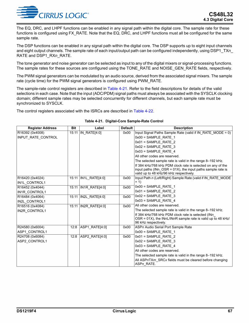
CS48L324.3 Digital Core
The EQ, DRC, and LHPF functions can be enabled in any signal path within the digital core. The sample rate for these functions is configured using FX_RATE. Note that the EQ, DRC, and LHPF functions must all be configured for the same sample rate.
The DSP functions can be enabled in any signal path within the digital core. The DSP supports up to eight input channels and eight output channels. The sample rate of each input/output path can be configured independently, using DSP1_TXn_RATE and DSP1_RXn_RATE.
The tone generator and noise generator can be selected as input to any of the digital mixers or signal-processing functions. The sample rates for these sources are configured using the TONE_RATE and NOISE_GEN_RATE fields, respectively.
The PWM signal generators can be modulated by an audio source, derived from the associated signal mixers. The sample rate (cycle time) for the PWM signal generators is configured using PWM_RATE.
The sample-rate control registers are described in Table 4-21. Refer to the field descriptions for details of the valid selections in each case. Note that the input (ADC/PDM) signal paths must always be associated with the SYSCLK clocking domain; different sample rates may be selected concurrently for different channels, but each sample rate must be synchronized to SYSCLK.
The control registers associated with the ISRCs are described in Table 4-22.
Table 4-21. Digital-Core Sample-Rate Control
Register Address Bit Label Default DescriptionR16392 (0x4008)INPUT_RATE_CONTROL
15:11 IN_RATE[4:0] 0x00 Input Signal Paths Sample Rate (valid if IN_RATE_MODE = 0)0x00 = SAMPLE_RATE_10x01 = SAMPLE_RATE_20x02 = SAMPLE_RATE_30x03 = SAMPLE_RATE_4All other codes are reserved.The selected sample rate is valid in the range 8–192 kHz.If 384 kHz/768 kHz PDM clock rate is selected on any of the input paths (INn_OSR = 01X), the input paths sample rate is valid up to 48 kHz/96 kHz respectively.
R16420 (0x4024)IN1L_CONTROL1
15:11 IN1L_RATE[4:0] 0x00 Input Path n (Left/Right) Sample Rate (valid if IN_RATE_MODE = 1)0x00 = SAMPLE_RATE_10x01 = SAMPLE_RATE_20x02 = SAMPLE_RATE_30x03 = SAMPLE_RATE_4All other codes are reserved.The selected sample rate is valid in the range 8–192 kHz.If 384 kHz/768 kHz PDM clock rate is selected (INn_OSR = 01X), the INnL/INnR sample rate is valid up to 48 kHz/96 kHz respectively.
R16452 (0x4044)IN1R_CONTROL1
15:11 IN1R_RATE[4:0] 0x00
R16484 (0x4064)IN2L_CONTROL1
15:11 IN2L_RATE[4:0] 0x00
R16516 (0x4084)IN2R_CONTROL1
15:11 IN2R_RATE[4:0] 0x00
R24580 (0x6004)ASP1_CONTROL1
12:8 ASP1_RATE[4:0] 0x00 ASPn Audio Serial Port Sample Rate0x00 = SAMPLE_RATE_10x01 = SAMPLE_RATE_20x02 = SAMPLE_RATE_30x03 = SAMPLE_RATE_4All other codes are reserved.The selected sample rate is valid in the range 8–192 kHz.All ASPnTXm_SRCx fields must be cleared before changing ASPn_RATE.
R24708 (0x6084)ASP2_CONTROL1
12:8 ASP2_RATE[4:0] 0x00
DS1219F4 Cirrus Logic 67
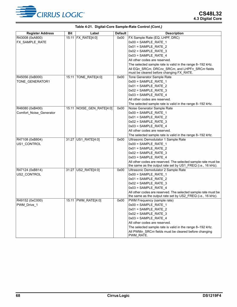
CS48L324.3 Digital Core
R43008 (0xA800)FX_SAMPLE_RATE
15:11 FX_RATE[4:0] 0x00 FX Sample Rate (EQ, LHPF, DRC)0x00 = SAMPLE_RATE_10x01 = SAMPLE_RATE_20x02 = SAMPLE_RATE_30x03 = SAMPLE_RATE_4All other codes are reserved.The selected sample rate is valid in the range 8–192 kHz.All EQn_SRCm, DRCnx_SRCm, and LHPFn_SRCm fields must be cleared before changing FX_RATE.
R45056 (0xB000)TONE_GENERATOR1
15:11 TONE_RATE[4:0] 0x00 Tone Generator Sample Rate0x00 = SAMPLE_RATE_10x01 = SAMPLE_RATE_20x02 = SAMPLE_RATE_30x03 = SAMPLE_RATE_4All other codes are reserved.The selected sample rate is valid in the range 8–192 kHz.
R46080 (0xB400)Comfort_Noise_Generator
15:11 NOISE_GEN_RATE[4:0] 0x00 Noise Generator Sample Rate0x00 = SAMPLE_RATE_10x01 = SAMPLE_RATE_20x02 = SAMPLE_RATE_30x03 = SAMPLE_RATE_4All other codes are reserved.The selected sample rate is valid in the range 8–192 kHz.
R47108 (0xB804)US1_CONTROL
31:27 US1_RATE[4:0] 0x00 Ultrasonic Demodulator 1 Sample Rate0x00 = SAMPLE_RATE_10x01 = SAMPLE_RATE_20x02 = SAMPLE_RATE_30x03 = SAMPLE_RATE_4All other codes are reserved. The selected sample rate must be the same as the output rate set by US1_FREQ (i.e., 16 kHz).
R47124 (0xB814)US2_CONTROL
31:27 US2_RATE[4:0] 0x00 Ultrasonic Demodulator 2 Sample Rate0x00 = SAMPLE_RATE_10x01 = SAMPLE_RATE_20x02 = SAMPLE_RATE_30x03 = SAMPLE_RATE_4All other codes are reserved. The selected sample rate must be the same as the output rate set by US2_FREQ (i.e., 16 kHz).
R49152 (0xC000)PWM_Drive_1
15:11 PWM_RATE[4:0] 0x00 PWM Frequency (sample rate)0x00 = SAMPLE_RATE_10x01 = SAMPLE_RATE_20x02 = SAMPLE_RATE_30x03 = SAMPLE_RATE_4All other codes are reserved.The selected sample rate is valid in the range 8–192 kHz.All PWMn_SRCm fields must be cleared before changing PWM_RATE.
Table 4-21. Digital-Core Sample-Rate Control (Cont.)
Register Address Bit Label Default Description
68 Cirrus Logic DS1219F4

CS48L324.3 Digital Core
4.3.12 Isochronous Sample-Rate Converter (ISRC)
The CS48L32 supports multiple signal paths through the digital core. The ISRCs provide sample-rate conversion between synchronized sample rates on the SYSCLK clock domain.
There are three ISRCs on the CS48L32. ISRC1 provides four signal paths between two different sample rates; ISRC2 and ISRC3 provide two signal paths between two different sample rates, as shown in Fig. 4-27. The sample rates associated with each ISRC can each be set equal to SAMPLE_RATE_1, SAMPLE_RATE_2, SAMPLE_RATE_3, or SAMPLE_RATE_4. See Section 4.8 for details of the sample-rate control registers.
Each ISRC converts between a sample rate selected by ISRCn_FSL and a sample rate selected by ISRCn_FSH, (where n identifies the applicable ISRC 1, 2, or 3). The higher of the two sample rates must be selected by ISRCn_FSH in each case.
The ISRCs support sample rates in the range 8–192 kHz. The sample-rate conversion ratio must be an integer (1–24) or equal to 1.5.
The ISRCn_FSL and ISRCn_FSH fields must not be changed if any of the respective x_SRCn fields is nonzero. The associated x_SRCn fields must be cleared before writing new values to ISRCn_FSL or ISRCn_FSH. A minimum delay of 125 s must be allowed between clearing the x_SRCn fields and writing to the associated ISRCn_FSL or ISRCn_FSH fields. See Table 4-22 for details.
The ISRC signal paths are enabled using the ISRCn_INTm_EN and ISRCn_DECm_EN bits, as follows:
0x2B80080DSP1_SAMPLE_RATE_RX1
4:0 DSP1_RX1_RATE[4:0] 0x00 DSP1 RX Channel n Sample Rate0x00 = SAMPLE_RATE_10x01 = SAMPLE_RATE_20x02 = SAMPLE_RATE_30x03 = SAMPLE_RATE_4All other codes are reserved.The selected sample rate is valid in the range 8–192 kHz.All DSP1RXn_SRCx fields must be cleared before changing DSP1_RXn_RATE.
0x2B80088DSP1_SAMPLE_RATE_RX2
4:0 DSP1_RX2_RATE[4:0] 0x00
0x2B80090DSP1_SAMPLE_RATE_RX3
4:0 DSP1_RX3_RATE[4:0] 0x00
0x2B80098DSP1_SAMPLE_RATE_RX4
4:0 DSP1_RX4_RATE[4:0] 0x00
0x2B800A0DSP1_SAMPLE_RATE_RX5
4:0 DSP1_RX5_RATE[4:0] 0x00
0x2B800A8DSP1_SAMPLE_RATE_RX6
4:0 DSP1_RX6_RATE[4:0] 0x00
0x2B800B0DSP1_SAMPLE_RATE_RX7
4:0 DSP1_RX7_RATE[4:0] 0x00
0x2B800B8DSP1_SAMPLE_RATE_RX8
4:0 DSP1_RX8_RATE[4:0] 0x00
0x2B80280DSP1_SAMPLE_RATE_TX1
4:0 DSP1_TX1_RATE[4:0] 0x00 DSP1 TX Channel n Sample Rate0x00 = SAMPLE_RATE_10x01 = SAMPLE_RATE_20x02 = SAMPLE_RATE_30x03 = SAMPLE_RATE_4All other codes are reserved.The selected sample rate is valid in the range 8–192 kHz.
0x2B80288DSP1_SAMPLE_RATE_TX2
4:0 DSP1_TX2_RATE[4:0] 0x00
0x2B80290DSP1_SAMPLE_RATE_TX3
4:0 DSP1_TX3_RATE[4:0] 0x00
0x2B80298DSP1_SAMPLE_RATE_TX4
4:0 DSP1_TX4_RATE[4:0] 0x00
0x2B802A0DSP1_SAMPLE_RATE_TX5
4:0 DSP1_TX5_RATE[4:0] 0x00
0x2B802A8DSP1_SAMPLE_RATE_TX6
4:0 DSP1_TX6_RATE[4:0] 0x00
0x2B802B0DSP1_SAMPLE_RATE_TX7
4:0 DSP1_TX7_RATE[4:0] 0x00
0x2B802B8DSP1_SAMPLE_RATE_TX8
4:0 DSP1_TX8_RATE[4:0] 0x00
Table 4-21. Digital-Core Sample-Rate Control (Cont.)
Register Address Bit Label Default Description
DS1219F4 Cirrus Logic 69

CS48L324.3 Digital Core
• The ISRCn interpolation paths (increasing sample rate) are enabled by setting the ISRCn_INTm_EN bits, (where m identifies the applicable channel).
• The ISRCn decimation paths (decreasing sample rate) are enabled by setting the ISRCn_DECm_EN bits.
The CS48L32 performs automatic checks to confirm that the SYSCLK frequency is high enough to support the commanded ISRC and digital mixing functions. If the frequency is too low, an attempt to enable an ISRC signal path fails. Note that active signal paths are not affected under such circumstances.
The status bits in registers 0x8080–0x907C indicate the status of each digital mixer. If an underclocked error condition occurs, these bits can be used to indicate which mixer paths have been enabled.
The ISRC signal paths and control registers are shown in Fig. 4-27.
Figure 4-27. Isochronous Sample-Rate Converters (ISRCs)
The ISRC input control fields (see Fig. 4-27) are located at addresses 0x8980 through 0x8AD0.
ISRCn_INT2_EN
ISRCn_INT3_EN
ISRCn_INT4_EN
ISRCn_INT1_ENISRCnINT1_SRC
ISRCnINT3_SRC
ISRCnINT4_SRC
ISRCnINT2_SRC
ISRC1 INT1 (0x098)ISRC2 INT1 (0x0A0)ISRC3 INT1 (0x0A8)
ISRC1 INT2 (0x099)ISRC2 INT2 (0x0A1)ISRC3 INT2 (0x0A9)
ISRC1 INT3 (0x09A)
ISRC1 INT4 (0x09B)
ISRCn_DEC2_EN
ISRCn_DEC3_EN
ISRCn_DEC4_EN
ISRCn_DEC1_EN ISRCnDEC1_SRC
ISRCnDEC3_SRC
ISRCnDEC4_SRC
ISRCnDEC2_SRC
ISRC1 DEC1 (0x09C)ISRC2 DEC1 (0x0A4)ISRC3 DEC1 (0x0AC)
ISRC1 DEC2 (0x09D)ISRC2 DEC2 (0x0A5)ISRC3 DEC2 (0x0AD)
ISRC1 DEC3 (0x09E)
ISRC1 DEC4 (0x09F)
ISRCn_FSL ISRCn_FSH
ISRC provides sample-rate conversions between synchronized sample rates on the SYSCLK domain.ISRCn_FSL identifies the lower of the two sample rates.ISRCn_FSH identifies the higher of the two sample rates.
…
…
…
…
…
…
…
…
CS48L32 supports three ISRC blocks, i.e., n = 1–3
70 Cirrus Logic DS1219F4

CS48L324.3 Digital Core
The full list of digital mixer control registers (0x8080–0x907C) is provided in Section 6. Generic register field definitions are provided in Table 4-10.
The x_SRC fields select the input sources for the respective ISRC processing blocks. Note that the selected input sources must be configured for the same sample rate as the ISRC to which they are connected.
The hexadecimal numbers in Fig. 4-27 indicate the corresponding x_SRC setting for selection of that signal as an input to another digital-core function.
The fields associated with the ISRCs are described in Table 4-22.
Table 4-22. Digital-Core ISRC Control
Register Address Bit Label Default DescriptionR41984 (0xA400)ISRC1_CONTROL1
31:27 ISRC1_FSL[4:0] 0x00 ISRC1 Low Sample Rate (Sets the lower of the ISRC1 sample rates)0x00 = SAMPLE_RATE_10x01 = SAMPLE_RATE_2
0x02 = SAMPLE_RATE_30x03 = SAMPLE_RATE_4
All other codes are reserved.The selected sample rate is valid in the range 8–192 kHz.All ISRC1_INTn_SRC fields must be cleared before changing ISRC1_FSL.
15:11 ISRC1_FSH[4:0] 0x00 ISRC1 High Sample Rate (Sets the higher of the ISRC1 sample rates)0x00 = SAMPLE_RATE_10x01 = SAMPLE_RATE_2
0x02 = SAMPLE_RATE_30x03 = SAMPLE_RATE_4
All other codes are reserved.The selected sample rate is valid in the range 8–192 kHz.All ISRC1_DECn_SRC fields must be cleared before changing ISRC1_FSH.
R41988 (0xA404)ISRC1_CONTROL2
11 ISRC1_INT4_EN 0 ISRC1 INT4 EnableInterpolation Channel 4 path from ISRC1_FSL rate to ISRC1_FSH rate0 = Disabled, 1 = Enabled
10 ISRC1_INT3_EN 0 ISRC1 INT3 EnableInterpolation Channel 3 path from ISRC1_FSL rate to ISRC1_FSH rate0 = Disabled, 1 = Enabled
9 ISRC1_INT2_EN 0 ISRC1 INT2 EnableInterpolation Channel 2 path from ISRC1_FSL rate to ISRC1_FSH rate0 = Disabled, 1 = Enabled
8 ISRC1_INT1_EN 0 ISRC1 INT1 EnableInterpolation Channel 1 path from ISRC1_FSL rate to ISRC1_FSH rate0 = Disabled, 1 = Enabled
3 ISRC1_DEC4_EN 0 ISRC1 DEC4 EnableDecimation Channel 4 path from ISRC1_FSH rate to ISRC1_FSL rate0 = Disabled, 1 = Enabled
2 ISRC1_DEC3_EN 0 ISRC1 DEC3 EnableDecimation Channel 3 path from ISRC1_FSH rate to ISRC1_FSL rate0 = Disabled, 1 = Enabled
1 ISRC1_DEC2_EN 0 ISRC1 DEC2 EnableDecimation Channel 2 path from ISRC1_FSH rate to ISRC1_FSL rate0 = Disabled, 1 = Enabled
0 ISRC1_DEC1_EN 0 ISRC1 DEC1 EnableDecimation Channel 1 path from ISRC1_FSH rate to ISRC1_FSL rate0 = Disabled, 1 = Enabled
DS1219F4 Cirrus Logic 71

CS48L324.4 DSP Firmware Control
4.4 DSP Firmware Control
The CS48L32 digital core incorporates a Halo Core DSP, capable of running a wide range of audio-enhancement functions. Different firmware configurations can be loaded onto the DSP, enabling the CS48L32 to be highly customized for specific application requirements. DSP firmware can be configured using software packages provided by Cirrus Logic, such as the SoundClear suite of audio-processing algorithms.
R42256 (0xA510)ISRC2_CONTROL1
31:27 ISRC2_FSH[4:0] 0x00 ISRC2 High Sample Rate (Sets the higher of the ISRC2 sample rates)0x00 = SAMPLE_RATE_10x01 = SAMPLE_RATE_2
0x02 = SAMPLE_RATE_30x03 = SAMPLE_RATE_4
All other codes are reserved.The selected sample rate is valid in the range 8–192 kHz.All ISRC2_DECn_SRC fields must be cleared before changing ISRC2_FSH.
15:11 ISRC2_FSL[4:0] 0x00 ISRC2 Low Sample Rate (Sets the lower of the ISRC2 sample rates)0x00 = SAMPLE_RATE_10x01 = SAMPLE_RATE_2
0x02 = SAMPLE_RATE_30x03 = SAMPLE_RATE_4
All other codes are reserved.The selected sample rate is valid in the range 8–192 kHz.All ISRC2_INTn_SRC fields must be cleared before changing ISRC2_FSL.
R42260 (0xA514)
ISRC2_CONTROL2
9 ISRC2_INT2_EN 0 ISRC2 INT2 EnableInterpolation Channel 2 path from ISRC2_FSL rate to ISRC2_FSH rate0 = Disabled, 1 = Enabled
8 ISRC2_INT1_EN 0 ISRC2 INT1 EnableInterpolation Channel 1 path from ISRC2_FSL rate to ISRC2_FSH rate0 = Disabled, 1 = Enabled
1 ISRC2_DEC2_EN 0 ISRC2 DEC2 EnableDecimation Channel 2 path from ISRC2_FSH rate to ISRC2_FSL rate0 = Disabled, 1 = Enabled
0 ISRC2_DEC1_EN 0 ISRC2 DEC1 EnableDecimation Channel 1 path from ISRC2_FSH rate to ISRC2_FSL rate0 = Disabled, 1 = Enabled
R42528 (0xA620)ISRC3_CONTROL1
31:27 ISRC3_FSH[4:0] 0x00 ISRC3 High Sample Rate (Sets the higher of the ISRC3 sample rates)0x00 = SAMPLE_RATE_10x01 = SAMPLE_RATE_2
0x02 = SAMPLE_RATE_30x03 = SAMPLE_RATE_4
All other codes are reserved.The selected sample rate is valid in the range 8–192 kHz.All ISRC3_DECn_SRC fields must be cleared before changing ISRC3_FSH.
15:11 ISRC3_FSL[4:0] 0x00 ISRC3 Low Sample Rate (Sets the lower of the ISRC3 sample rates)0x00 = SAMPLE_RATE_10x01 = SAMPLE_RATE_2
0x02 = SAMPLE_RATE_30x03 = SAMPLE_RATE_4
All other codes are reserved.The selected sample rate is valid in the range 8–192 kHz.All ISRC3_INTn_SRC fields must be cleared before changing ISRC3_FSL.
R42532 (0xA624)
ISRC3_CONTROL2
9 ISRC3_INT2_EN 0 ISRC3 INT2 EnableInterpolation Channel 2 path from ISRC3_FSL rate to ISRC3_FSH rate0 = Disabled, 1 = Enabled
8 ISRC3_INT1_EN 0 ISRC3 INT1 EnableInterpolation Channel 1 path from ISRC3_FSL rate to ISRC3_FSH rate0 = Disabled, 1 = Enabled
1 ISRC3_DEC2_EN 0 ISRC3 DEC2 EnableDecimation Channel 2 path from ISRC3_FSH rate to ISRC3_FSL rate0 = Disabled, 1 = Enabled
0 ISRC3_DEC1_EN 0 ISRC3 DEC1 EnableDecimation Channel 1 path from ISRC3_FSH rate to ISRC3_FSL rate0 = Disabled, 1 = Enabled
Table 4-22. Digital-Core ISRC Control (Cont.)
Register Address Bit Label Default Description
72 Cirrus Logic DS1219F4

CS48L324.4 DSP Firmware Control
The DSP is designed specifically for audio applications, employing a small gate-count architecture to support an optimized mix of processing features while fulfilling a low power-consumption requirement. The instruction set is highly efficient and targeted, with a high degree of parallelism and efficient multicore integration to reduce power consumption and increase processing speed.
The DSP core incorporates two data memories supporting high-bandwidth access: parallel memory access can fetch two short (24-bit) operands per memory per cycle; simultaneous memory access enables up to four 24-bit accesses per clock cycle. Multiple data formats are supported, including basic 24-bit register and 56-bit accumulator. Native support for 48-bit double-precision calculations is also provided.
The DSP core is supported by an interrupt controller (up to 24 inputs), JTAG debugger, memory protection unit (MPU) with error-trace stack, and watchdog timer. Arbitrated multiple-access to the program and data memories is provided, with support for configurable FFT, FIR, LMS, and linear/dB-conversion accelerators. Note that different instances of the Halo Core DSP may provide different feature sets; specific details for the CS48L32 are provided in Section 4.4.1.
To use the programmable DSP, the required firmware configuration must first be loaded onto the device by writing the appropriate files to the CS48L32 register map; the firmware configuration comprises program and data memory contents. After loading the DSP firmware, the DSP functions must be enabled using the associated control fields.
Details of the DSP firmware memory registers are provided in Section 4.4.2. Note that the WISCE evaluation board control software provides support for loading the CS48L32 program and data memories. A software programming guide can be provided to assist users in developing their own software algorithms—please contact your Cirrus Logic representative for further information.
The audio signal paths to and from the DSP processing block are configured as described in Section 4.3. Note that the DSP firmware must be loaded and enabled before audio signal paths can be enabled.
4.4.1 DSP Configuration Definition
The Halo Core DSP uses an adaptable design that can be tailored to suit different target applications. Each instance of the DSP (either on a single device, or from one device to another) may offer different capabilities in terms of memory size, hardware accelerators, and other features.
The parameters defining the CS48L32 Halo Core DSP are described in Table 4-23.
Table 4-23. Halo Core DSP Definition
Description DSP1
Start address in device register map 0x200_0000X-memory bank size (number of 48-bit words) 4096Y-memory bank size (number of 48-bit words) 4096P-memory bank size (number of 40-bit words) 8192Boot-memory bank size (number of 40-bit words) 8192Address offset for PM (packed) 0x0180_0000Address offset for XM (packed, 32-bit) 0x0000_0000Address offset for YM (packed, 32-bit) 0x00C0_0000Address offset for XM (unpacked, 24-bit) 0x0080_0000Address offset for YM (unpacked, 24-bit) 0x0140_0000Address offset for XM (unpacked, 32-bit) 0x0040_0000Address offset for YM (unpacked, 32-bit) 0x0100_0000Number of external debug triggers 0JTAG debug ID 1Maximum clock speed 100 MHzAccelerator functions—dB/linear converters YesLMS (least mean square) filters 5FIR (finite impulse response) filters 8FFT (fast Fourier transform) accelerators YesMIPS profiler Yes
DS1219F4 Cirrus Logic 73
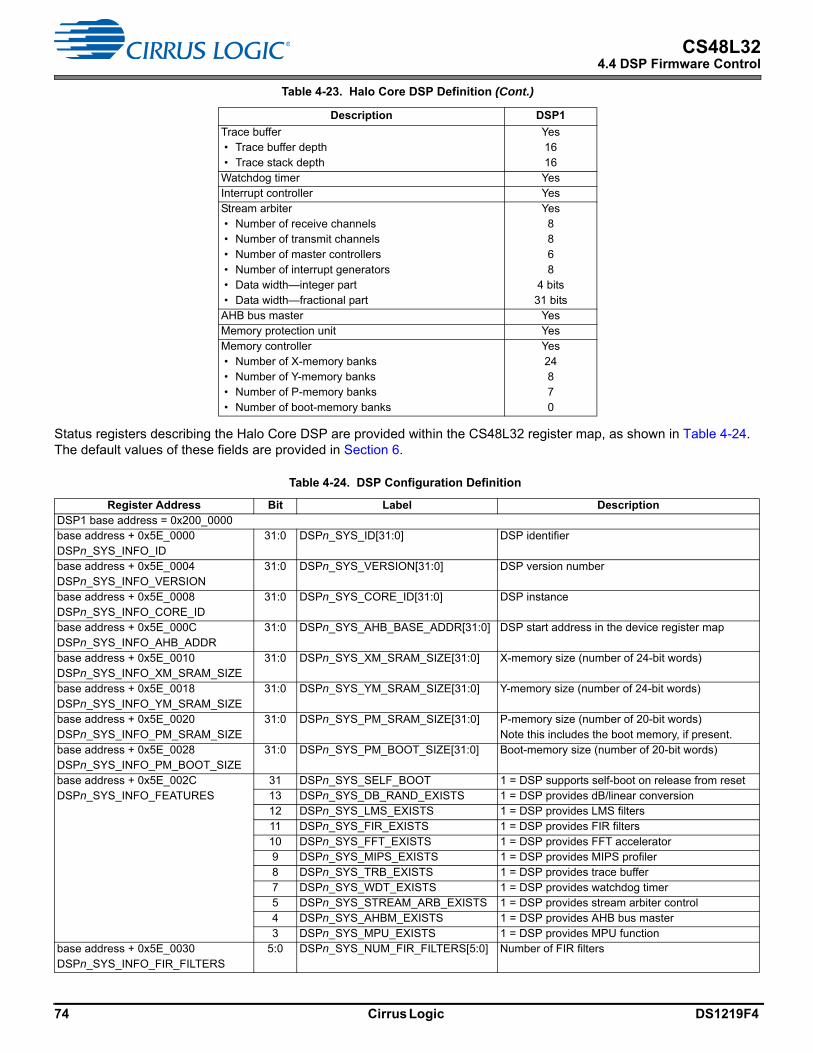
CS48L324.4 DSP Firmware Control
Status registers describing the Halo Core DSP are provided within the CS48L32 register map, as shown in Table 4-24. The default values of these fields are provided in Section 6.
Trace buffer • Trace buffer depth • Trace stack depth
Yes1616
Watchdog timer YesInterrupt controller YesStream arbiter • Number of receive channels • Number of transmit channels • Number of master controllers • Number of interrupt generators • Data width—integer part • Data width—fractional part
Yes8868
4 bits31 bits
AHB bus master YesMemory protection unit YesMemory controller • Number of X-memory banks • Number of Y-memory banks • Number of P-memory banks • Number of boot-memory banks
Yes24870
Table 4-24. DSP Configuration Definition
Register Address Bit Label DescriptionDSP1 base address = 0x200_0000base address + 0x5E_0000DSPn_SYS_INFO_ID
31:0 DSPn_SYS_ID[31:0] DSP identifier
base address + 0x5E_0004DSPn_SYS_INFO_VERSION
31:0 DSPn_SYS_VERSION[31:0] DSP version number
base address + 0x5E_0008DSPn_SYS_INFO_CORE_ID
31:0 DSPn_SYS_CORE_ID[31:0] DSP instance
base address + 0x5E_000CDSPn_SYS_INFO_AHB_ADDR
31:0 DSPn_SYS_AHB_BASE_ADDR[31:0] DSP start address in the device register map
base address + 0x5E_0010DSPn_SYS_INFO_XM_SRAM_SIZE
31:0 DSPn_SYS_XM_SRAM_SIZE[31:0] X-memory size (number of 24-bit words)
base address + 0x5E_0018DSPn_SYS_INFO_YM_SRAM_SIZE
31:0 DSPn_SYS_YM_SRAM_SIZE[31:0] Y-memory size (number of 24-bit words)
base address + 0x5E_0020DSPn_SYS_INFO_PM_SRAM_SIZE
31:0 DSPn_SYS_PM_SRAM_SIZE[31:0] P-memory size (number of 20-bit words)Note this includes the boot memory, if present.
base address + 0x5E_0028DSPn_SYS_INFO_PM_BOOT_SIZE
31:0 DSPn_SYS_PM_BOOT_SIZE[31:0] Boot-memory size (number of 20-bit words)
base address + 0x5E_002CDSPn_SYS_INFO_FEATURES
31 DSPn_SYS_SELF_BOOT 1 = DSP supports self-boot on release from reset13 DSPn_SYS_DB_RAND_EXISTS 1 = DSP provides dB/linear conversion12 DSPn_SYS_LMS_EXISTS 1 = DSP provides LMS filters11 DSPn_SYS_FIR_EXISTS 1 = DSP provides FIR filters10 DSPn_SYS_FFT_EXISTS 1 = DSP provides FFT accelerator9 DSPn_SYS_MIPS_EXISTS 1 = DSP provides MIPS profiler8 DSPn_SYS_TRB_EXISTS 1 = DSP provides trace buffer7 DSPn_SYS_WDT_EXISTS 1 = DSP provides watchdog timer5 DSPn_SYS_STREAM_ARB_EXISTS 1 = DSP provides stream arbiter control4 DSPn_SYS_AHBM_EXISTS 1 = DSP provides AHB bus master3 DSPn_SYS_MPU_EXISTS 1 = DSP provides MPU function
base address + 0x5E_0030DSPn_SYS_INFO_FIR_FILTERS
5:0 DSPn_SYS_NUM_FIR_FILTERS[5:0] Number of FIR filters
Table 4-23. Halo Core DSP Definition (Cont.)
Description DSP1
74 Cirrus Logic DS1219F4

CS48L324.4 DSP Firmware Control
4.4.2 DSP Firmware Memory and Register Mapping
The DSP firmware memory comprises program memory (P-memory) and two regions of data memory (X-memory and Y-memory). Each memory (X, Y, or P) is arranged as a number of banks; the size of each is defined by the bank size and the number or banks as shown in Table 4-23. The banked configuration enables each memory to support multiple simultaneous read/write accesses.
The program memory is formatted as 40-bit words. Most of the processor functionality uses 20-bit instructions, but some make use of the 40-bit width. Referenced to the CS48L32 register map, blocks of four 40-bit words are packed into five 32-bit registers.
The data memory is formatted as 24-bit words. Each of the data memories is mapped to three different locations of the CS48L32 register map, with a different packing layout used in each case; this provides flexibility to access the data memory in different ways according to the specific task that is being performed. Note that the three sections all represent the same data—data that is written to one section can be read back either at the same address or at the corresponding address within either of the other sections.
• In the packed data-memory, blocks of four 24-bit words are packed into three 32-bit registers. This tightly-packed layout does not include any padding bits; it provides efficient access to the data memory, ideal for transfer of large volumes of audio data.
• In the unpacked 24-bit memory, each 24-bit data word occupies one 32-bit register; the MSBs of each register are unused. This layout is ideal for read/write access to individual 24-bit words.
• In the unpacked 32-bit memory, 32-bit data is supported in 32-bit registers. Each 32-bit data word uses the space of two 24-bit words in the DSP memory. This provides support for 32-bit data within the 24-bit X- or Y-memory regions. Note that the usable capacity of the data memory is reduced in this format, as some bits are not used.
The CS48L32 program- and data-register memory space is described in Table 4-25. The full register map listing is provided in Section 6.
The DSP firmware memory is configured by writing to the registers referenced in Table 4-25. Note that clocking is not required for access to the firmware registers by the host processor.
4.4.3 DSP Firmware Control
The configuration and control of the DSP firmware is described in the following subsections.
base address + 0x5E_0034DSPn_SYS_INFO_LMS_FILTERS
5:0 DSPn_SYS_NUM_LMS_FILTERS[5:0] Number of LMS filters
base address + 0x5E_0038DSPn_SYS_INFO_XM_BANK_SIZE
31:0 DSPn_SYS_XM_BANK_SIZE[31:0] X-memory bank size (number of 24-bit words)
base address + 0x5E_003CDSPn_SYS_INFO_YM_BANK_SIZE
31:0 DSPn_SYS_YM_BANK_SIZE[31:0] Y-memory bank size (number of 24-bit words)
base address + 0x5E_0040DSPn_SYS_INFO_PM_BANK_SIZE
31:0 DSPn_SYS_PM_BANK_SIZE[31:0] P-memory bank size (number of 20-bit words)
Table 4-25. DSP Program, Data, and Coefficient Registers
DSP Number Description Register Address Number of Registers DSP Memory SizeDSP1 Program memory 0x380_0000–0x384_5FFC 71680 56k x 40-bit words
X-memory PackedUnpacked-24Unpacked-32
0x200_0000–0x208_FFFC0x280_0000–0x28B_FFFC0x240_0000–0x245_FFFC
14745619660898304
192k x 24-bit words192k x 24-bit words96k x 32-bit words
Y-memory PackedUnpacked-24Unpacked-32
0x2C0_0000–0x2C2_FFFC0x340_0000–0x343_FFFC0x300_0000–0x301_FFFC
491526553632768
64k x 24-bit words64k x 24-bit words32k x 32-bit words
Table 4-24. DSP Configuration Definition (Cont.)
Register Address Bit Label Description
DS1219F4 Cirrus Logic 75

CS48L324.4 DSP Firmware Control
4.4.3.1 DSP Memory
The DSP firmware memory comprises program memory (P-memory) and data memory (X-memory and Y-memory) as described in Section 4.4.2. Each memory (X, Y, or P) is arranged as a number of banks; the banked configuration enables each memory to support multiple simultaneous read/write accesses.
Each bank of memory can be individually enabled or disabled; the power consumption of the firmware memory can be optimized by enabling only the banks that are required for a particular application.
The CS48L32 firmware memory also supports a low-power retention state; in this state, the memory contents are retained, but read/write access is not supported. The low-power retention state is selectable for each memory region (P, X, or Y), and applies to all enabled banks of the respective memory.
The DSP firmware memory is controlled using the x_PWD_N and x_EXT_N_n fields described in Table 4-27. Separate controls are provided for odd-numbered and even-numbered words within each memory region.
• x_PWD_N selects the active or data-retention state for the respective memory. In the active state, read/write access is supported. In the data-retention state, the memory contents are maintained, but read/write access is not possible.
• x_EXT_N_n selects the enabled or disabled state for the respective memory bank n. If the bank is disabled, the contents are lost. If the bank is enabled, read/write access is supported (provided the respective memory is active).
The memory-control fields are summarized in Table 4-26.
Notes: If a memory bank is disabled, the contents of this bank are lost—the low-power retention state is not valid fordisabled memory banks. The memory is not actively cleared in the disabled state—some contents of the memorymay persist in the disabled state, but the integrity of the memory contents is not assured.
If a memory bank is disabled, all higher-numbered banks in the same memory (X, Y, or P) are unavailable. It is recommended to disable the higher-numbered banks by clearing the respective x_EXT_N_n bits.
The DSP memory-control fields are not affected by software reset; these bits remain in their previous state under software-reset conditions. The DSP firmware memory contents are maintained through software reset, provided the respective memory bank is enabled.
The DSP1 memory-control fields are defined in Table 4-27.
Table 4-26. DSP Memory Control
x_PWD_N x_EXT_N_n Description0 0 Memory disabled, contents lost0 1 Memory enabled in data-retention state1 0 Memory disabled, contents lost1 1 Memory enabled for read/write access
Table 4-27. DSP Memory Control Registers
Register Address Bit Label Default DescriptionR94220 (0x1700C)DSP1_XM_SRAM_IBUS_SETUP_0
1 DSP1_XM_SRAM_IBUS_E_PWD_N 0 X-memory even-address power control0 = Data-retention state1 = Memory activeOnly valid for enabled memory banks
0 DSP1_XM_SRAM_IBUS_O_PWD_N 0 X-memory odd-address power control0 = Data-retention state1 = Memory activeOnly valid for enabled memory banks
R94224 (0x17010)DSP1_XM_SRAM_IBUS_SETUP_1toR94316 (0x1706C)DSP1_XM_SRAM_IBUS_SETUP_24
1 DSP1_XM_SRAM_IBUS_E_EXT_N_n 0 X-memory even-address Bank n enable0 = Disabled1 = Enabled
0 DSP1_XM_SRAM_IBUS_O_EXT_N_n 0 X-memory odd-address Bank n enable0 = Disabled1 = Enabled
76 Cirrus Logic DS1219F4

CS48L324.4 DSP Firmware Control
The firmware memory contents are maintained through software reset. The DSP firmware memory contents are not retained under power-on-reset or hardware-reset conditions.
Note that the DSP firmware memory is not actively cleared under power-on-reset or hardware-reset conditions; some contents of the memory may persist through these events, but the integrity of the memory is not assured.
See Section 4.14 for details of the CS48L32 reset functions.
4.4.3.2 DSP Clocking
A clock signal is required when executing software on the DSP core, or if any of the stream-arbiter master controllers is enabled. (Note that clocking is not required for access to the firmware registers by the host processor.)
The clock source for the DSP is derived from SYSCLK. See Section 4.8 for details of how to configure SYSCLK. Note that the internal clock signals within the DSP are enabled and disabled automatically, as required by the DSP-core and stream-arbiter status.
The DSP clock frequency is selected using DSP1_CLK_FREQ_SEL. Note that the clock frequency must be less than or equal to the SYSCLK frequency.
The DSP1_CLK_FREQ_STS field indicates the clock frequency for the DSP core. This can be used to confirm the clock frequency—for example, in cases where code execution has a minimum clock-frequency requirement. Note that DSP1_CLK_FREQ_STS is only valid while the core is running code; typical usage of this field would be for the DSP core to read the clock status and to take action as applicable, in particular, if the available clock does not meet the application requirements.
Note that, depending on the clock-source frequency and the available dividers, the DSP1 clock frequency may differ from the selected frequency. In most cases, the DSP1 clock frequency equals or exceeds the requested frequency. A lower frequency is implemented if limited by either the clock-source frequency or the maximum DSP1 clocking frequency.
R94320 (0x17070)DSP1_YM_SRAM_IBUS_SETUP_0
1 DSP1_YM_SRAM_IBUS_E_PWD_N 0 Y-memory even-address power control0 = Data-retention state1 = Memory activeOnly valid for enabled memory banks
0 DSP1_YM_SRAM_IBUS_O_PWD_N 0 Y-memory odd-address power control0 = Data-retention state1 = Memory activeOnly valid for enabled memory banks
R94324 (0x17074)DSP1_YM_SRAM_IBUS_SETUP_1toR94352 (0x17090)DSP1_YM_SRAM_IBUS_SETUP_8
1 DSP1_YM_SRAM_IBUS_E_EXT_N_n 0 Y-memory even-address Bank n enable0 = Disabled1 = Enabled
0 DSP1_YM_SRAM_IBUS_O_EXT_N_n 0 Y-memory odd-address Bank n enable0 = Disabled1 = Enabled
R94356 (0x17094)DSP1_PM_SRAM_IBUS_SETUP_0
1 DSP1_PM_SRAM_IBUS_E_PWD_N 0 P-memory even-address power control0 = Data-retention state1 = Memory activeOnly valid for enabled memory banks
0 DSP1_PM_SRAM_IBUS_O_PWD_N 0 P-memory odd-address power control0 = Data-retention state1 = Memory activeOnly valid for enabled memory banks
R94360 (0x17098)DSP1_PM_SRAM_IBUS_SETUP_1toR94384 (0x170B0)DSP1_PM_SRAM_IBUS_SETUP_7
1 DSP1_PM_SRAM_IBUS_E_EXT_N_n 0 P-memory even-address Bank n enable0 = Disabled1 = Enabled
0 DSP1_PM_SRAM_IBUS_O_EXT_N_n 0 P-memory odd-address Bank n enable0 = Disabled1 = Enabled
Table 4-27. DSP Memory Control Registers (Cont.)
Register Address Bit Label Default Description
DS1219F4 Cirrus Logic 77
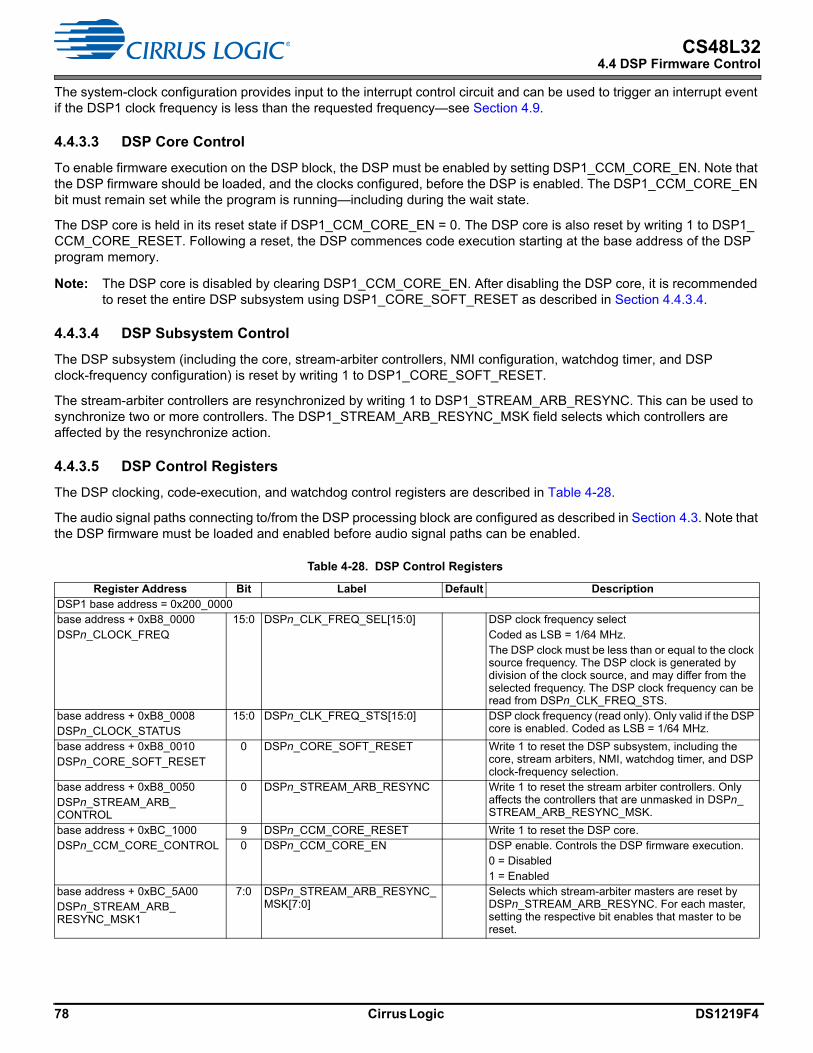
CS48L324.4 DSP Firmware Control
The system-clock configuration provides input to the interrupt control circuit and can be used to trigger an interrupt event if the DSP1 clock frequency is less than the requested frequency—see Section 4.9.
4.4.3.3 DSP Core Control
To enable firmware execution on the DSP block, the DSP must be enabled by setting DSP1_CCM_CORE_EN. Note that the DSP firmware should be loaded, and the clocks configured, before the DSP is enabled. The DSP1_CCM_CORE_EN bit must remain set while the program is running—including during the wait state.
The DSP core is held in its reset state if DSP1_CCM_CORE_EN = 0. The DSP core is also reset by writing 1 to DSP1_CCM_CORE_RESET. Following a reset, the DSP commences code execution starting at the base address of the DSP program memory.
Note: The DSP core is disabled by clearing DSP1_CCM_CORE_EN. After disabling the DSP core, it is recommended to reset the entire DSP subsystem using DSP1_CORE_SOFT_RESET as described in Section 4.4.3.4.
4.4.3.4 DSP Subsystem Control
The DSP subsystem (including the core, stream-arbiter controllers, NMI configuration, watchdog timer, and DSP clock-frequency configuration) is reset by writing 1 to DSP1_CORE_SOFT_RESET.
The stream-arbiter controllers are resynchronized by writing 1 to DSP1_STREAM_ARB_RESYNC. This can be used to synchronize two or more controllers. The DSP1_STREAM_ARB_RESYNC_MSK field selects which controllers are affected by the resynchronize action.
4.4.3.5 DSP Control Registers
The DSP clocking, code-execution, and watchdog control registers are described in Table 4-28.
The audio signal paths connecting to/from the DSP processing block are configured as described in Section 4.3. Note that the DSP firmware must be loaded and enabled before audio signal paths can be enabled.
Table 4-28. DSP Control Registers
Register Address Bit Label Default DescriptionDSP1 base address = 0x200_0000base address + 0xB8_0000DSPn_CLOCK_FREQ
15:0 DSPn_CLK_FREQ_SEL[15:0] DSP clock frequency selectCoded as LSB = 1/64 MHz.The DSP clock must be less than or equal to the clock source frequency. The DSP clock is generated by division of the clock source, and may differ from the selected frequency. The DSP clock frequency can be read from DSPn_CLK_FREQ_STS.
base address + 0xB8_0008DSPn_CLOCK_STATUS
15:0 DSPn_CLK_FREQ_STS[15:0] DSP clock frequency (read only). Only valid if the DSP core is enabled. Coded as LSB = 1/64 MHz.
base address + 0xB8_0010DSPn_CORE_SOFT_RESET
0 DSPn_CORE_SOFT_RESET Write 1 to reset the DSP subsystem, including the core, stream arbiters, NMI, watchdog timer, and DSP clock-frequency selection.
base address + 0xB8_0050DSPn_STREAM_ARB_CONTROL
0 DSPn_STREAM_ARB_RESYNC Write 1 to reset the stream arbiter controllers. Only affects the controllers that are unmasked in DSPn_STREAM_ARB_RESYNC_MSK.
base address + 0xBC_1000DSPn_CCM_CORE_CONTROL
9 DSPn_CCM_CORE_RESET Write 1 to reset the DSP core.0 DSPn_CCM_CORE_EN DSP enable. Controls the DSP firmware execution.
0 = Disabled1 = Enabled
base address + 0xBC_5A00DSPn_STREAM_ARB_RESYNC_MSK1
7:0 DSPn_STREAM_ARB_RESYNC_MSK[7:0]
Selects which stream-arbiter masters are reset by DSPn_STREAM_ARB_RESYNC. For each master, setting the respective bit enables that master to be reset.
78 Cirrus Logic DS1219F4

CS48L324.5 DSP Peripheral Control
4.4.4 DSP Interrupts
The Halo Core DSP incorporates a comprehensive interrupt controller, supporting a flexible capability to take input from many different events and status indications, and to adapt the program flow according to different priority levels assigned to each event. A high-priority non-maskable interrupt (NMI) is provided in case of a serious failure mode requiring a reset of the DSP.
The DSP also provides input to the device-level interrupt controller. The DSP-derived inputs to the CS48L32 interrupt controller include DSP error indications and general-purpose interrupt signals under control of the DSP firmware.
The following events are supported as inputs to the CS48L32 interrupt controller:
• Memory protection error
• Watchdog timeout
• Memory controller error
• AHB system error
• AHB packing error
• NMI error
• General-purpose IRQ 0–3
• Trace buffer stack error
• MIPS profile 1 done
• MIPS profile 0 done
See Section 4.9 for further details of the CS48L32 interrupt controller.
4.5 DSP Peripheral Control
The CS48L32 incorporates a suite of DSP peripheral functions that can be integrated together to provide an enhanced capability for DSP applications. Configurable event log functions provide multichannel monitoring of internal and external signals. The general-purpose timers provide time-stamp data for the event logger; they also provide input to the alarm-generator circuits, enabling time-dependent interrupt events to be generated. Maskable GPIO provides an efficient mechanism for the Halo Core DSP to access the required input and output signals. The quad-SPI (QSPI) master interface enables high-speed data transfers between the DSP and external components such as flash-memory devices.
The DSP peripherals are designed to provide a comprehensive DSP capability, operating with a high degree of autonomy from the host processor.
4.5.1 Event Logger
The CS48L32 provides an event-log function, supporting multichannel, edge-sensitive monitoring and recording of internal or external signals.
4.5.1.1 Overview
The event logger allows status information to be captured from a large number of sources, to be prioritized and acted upon as required. For the purposes of the event logger, an event is recorded when a logic transition (edge) is detected on a selected signal source.
The logged events are held in a FIFO buffer, which is managed by the application software. A 32-bit time stamp, derived from one of the general-purpose timers, is associated and recorded with each FIFO index, to provide a comprehensive record of the detected events.
The event logger is associated with one of the general-purpose timers (see Section 4.5.3). The selected timer is the source of time stamp data for any logged events.
DS1219F4 Cirrus Logic 79
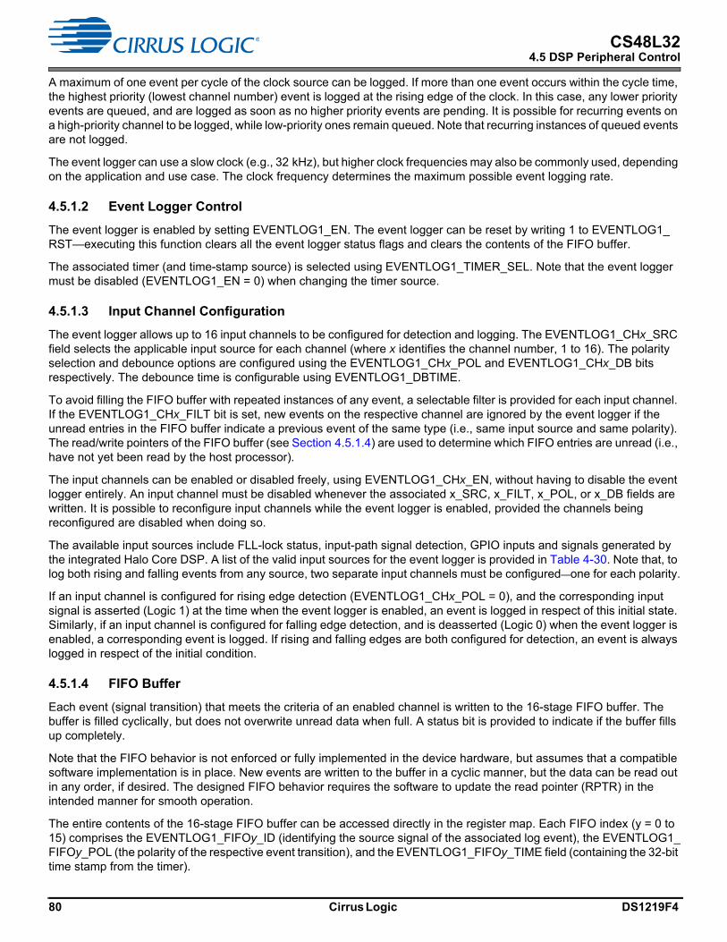
CS48L324.5 DSP Peripheral Control
A maximum of one event per cycle of the clock source can be logged. If more than one event occurs within the cycle time, the highest priority (lowest channel number) event is logged at the rising edge of the clock. In this case, any lower priority events are queued, and are logged as soon as no higher priority events are pending. It is possible for recurring events on a high-priority channel to be logged, while low-priority ones remain queued. Note that recurring instances of queued events are not logged.
The event logger can use a slow clock (e.g., 32 kHz), but higher clock frequencies may also be commonly used, depending on the application and use case. The clock frequency determines the maximum possible event logging rate.
4.5.1.2 Event Logger Control
The event logger is enabled by setting EVENTLOG1_EN. The event logger can be reset by writing 1 to EVENTLOG1_RST—executing this function clears all the event logger status flags and clears the contents of the FIFO buffer.
The associated timer (and time-stamp source) is selected using EVENTLOG1_TIMER_SEL. Note that the event logger must be disabled (EVENTLOG1_EN = 0) when changing the timer source.
4.5.1.3 Input Channel Configuration
The event logger allows up to 16 input channels to be configured for detection and logging. The EVENTLOG1_CHx_SRC field selects the applicable input source for each channel (where x identifies the channel number, 1 to 16). The polarity selection and debounce options are configured using the EVENTLOG1_CHx_POL and EVENTLOG1_CHx_DB bits respectively. The debounce time is configurable using EVENTLOG1_DBTIME.
To avoid filling the FIFO buffer with repeated instances of any event, a selectable filter is provided for each input channel. If the EVENTLOG1_CHx_FILT bit is set, new events on the respective channel are ignored by the event logger if the unread entries in the FIFO buffer indicate a previous event of the same type (i.e., same input source and same polarity). The read/write pointers of the FIFO buffer (see Section 4.5.1.4) are used to determine which FIFO entries are unread (i.e., have not yet been read by the host processor).
The input channels can be enabled or disabled freely, using EVENTLOG1_CHx_EN, without having to disable the event logger entirely. An input channel must be disabled whenever the associated x_SRC, x_FILT, x_POL, or x_DB fields are written. It is possible to reconfigure input channels while the event logger is enabled, provided the channels being reconfigured are disabled when doing so.
The available input sources include FLL-lock status, input-path signal detection, GPIO inputs and signals generated by the integrated Halo Core DSP. A list of the valid input sources for the event logger is provided in Table 4-30. Note that, to log both rising and falling events from any source, two separate input channels must be configured—one for each polarity.
If an input channel is configured for rising edge detection (EVENTLOG1_CHx_POL = 0), and the corresponding input signal is asserted (Logic 1) at the time when the event logger is enabled, an event is logged in respect of this initial state. Similarly, if an input channel is configured for falling edge detection, and is deasserted (Logic 0) when the event logger is enabled, a corresponding event is logged. If rising and falling edges are both configured for detection, an event is always logged in respect of the initial condition.
4.5.1.4 FIFO Buffer
Each event (signal transition) that meets the criteria of an enabled channel is written to the 16-stage FIFO buffer. The buffer is filled cyclically, but does not overwrite unread data when full. A status bit is provided to indicate if the buffer fills up completely.
Note that the FIFO behavior is not enforced or fully implemented in the device hardware, but assumes that a compatible software implementation is in place. New events are written to the buffer in a cyclic manner, but the data can be read out in any order, if desired. The designed FIFO behavior requires the software to update the read pointer (RPTR) in the intended manner for smooth operation.
The entire contents of the 16-stage FIFO buffer can be accessed directly in the register map. Each FIFO index (y = 0 to 15) comprises the EVENTLOG1_FIFOy_ID (identifying the source signal of the associated log event), the EVENTLOG1_FIFOy_POL (the polarity of the respective event transition), and the EVENTLOG1_FIFOy_TIME field (containing the 32-bit time stamp from the timer).
80 Cirrus Logic DS1219F4

CS48L324.5 DSP Peripheral Control
The FIFO buffer is managed using EVENTLOG1_FIFO_WPTR and EVENTLOG1_FIFO_RPTR. The write pointer (WPTR) field identifies the index location (0 to 15) in which the next event is logged. The read pointer (RPTR) field identifies the index location of the first set of unread data, if any exists. Both of these fields are initialized to 0 when the event logger is reset.
• If RPTR WPTR, the buffer contains new data. The number of new events is equal to the difference between the two pointer values (WPTR – RPTR, allowing for wraparound beyond Index 15). For example, if WPTR = 12 and RPTR = 8, this means that there are four unread data sets in the buffer, at index locations 8, 9, 10, and 11.
After reading the new data from the buffer, the RPTR value should be incremented by the corresponding amount (e.g., increment by 4, in the example described above). Note that the RPTR value can either be incremented once for each read, or can be incremented in larger steps after a batch read.
• If RPTR = WPTR, the buffer is either empty (0 events) or full (16 events). In this case, the status bits described in Section 4.5.1.5 confirm the current status of the buffer.
4.5.1.5 Status Bits
The EVENTLOG1_CHx_STS bits indicate the status of the source signal for the respective input channel.
The EVENTLOG1_NOT_EMPTY bit indicates whether the FIFO buffer is empty. If this bit is set, it indicates one or more new sets of data in the FIFO.
The EVENTLOG1_WMARK_STS bit indicates when the number of FIFO index locations available for new events reaches a configurable threshold, known as the watermark level. The watermark level is held in the EVENTLOG1_FIFO_WMARK field.
The EVENTLOG1_FULL bit indicates when the FIFO buffer is full. If this bit is set, it indicates that there are 16 sets of new event data in the FIFO. Note that this does not mean that a buffer overflow condition has occurred, but further events are not logged or indicated until the buffer has been cleared.
Note: Following a buffer full condition, the FIFO operation resumes as soon as the RPTR field has been updated to a new value. Writing the same value to RPTR does not restart the FIFO operation, even if the entire buffer contents have been read. After all of the required data has been read from the buffer, the RPTR value should be set equal to the WPTR value; an intermediate (different) value must also be written to the RPTR field in order to clear the buffer full status and restart the FIFO operation.
4.5.1.6 Interrupts
The event log status flags are inputs to the interrupt control circuit and can be used to trigger an interrupt event when the FIFO-full condition occurs—see Section 4.9.
4.5.1.7 Event Logger Control Registers
The event logger control registers are described in Table 4-29.
DS1219F4 Cirrus Logic 81

CS48L324.5 DSP Peripheral Control
Table 4-29. Event Logger (EVENTLOG1) Control
Register Address Bit Label Default DescriptionR1114112 (0x110000)EVENTLOG1_CONTROL
19:16 EVENTLOG1_DBTIME[3:0] 0x0 Event Log input debounce0x0 = 93.75 s0x1 = 1.5 ms0x2 = 3 ms0x3 = 6 ms0x4 = 12 ms0x5 = 24 ms
0x6 = 48 ms0x7 = 96 ms0x8 = 192 ms0x9 = 384 ms0xA = 768 ms0xB–0xF = Reserved
8 EVENTLOG1_DSP_CLK_EN 0 Event Log clock control0 = Disabled1 = EnabledIf this bit is set, SYSCLK is enabled whenever the Event Log FIFO buffer is not empty—this allows the Event Log to process events if the system clock is disabled.
1 EVENTLOG1_RST 0 Event Log ResetWrite 1 to reset the status outputs and clear the FIFO buffer.
0 EVENTLOG1_EN 0 Event Log Enable0 = Disabled1 = Enabled
R1114120 (0x110008)EVENTLOG1_TIMER_SEL
0 EVENTLOG1_TIMER_SEL 0 Event Log Timer Source Select0 = Timer 11 = Timer 2Note that the event log must be disabled when updating this field.
R1114136 (0x110018)EVENTLOG1_FIFO_CONTROL1
3:0 EVENTLOG1_FIFO_WMARK[3:0]
0x1 Event Log FIFO Watermark. The watermark status output is asserted when the number of FIFO locations available for new events is less than or equal to the FIFO watermark.Valid from 0 to 15.
R1114140 (0x11001C)EVENTLOG1_FIFO_POINTER1
18 EVENTLOG1_FULL 0 Event Log FIFO Full Status. This bit, when set, indicates that the FIFO buffer is full. It is cleared when a new value is written to the FIFO read pointer, or when the event log is Reset.
17 EVENTLOG1_WMARK_STS 0 Event Log FIFO Watermark Status. This bit, when set, indicates that the FIFO space available for new events to be logged is less than or equal to the watermark threshold.
16 EVENTLOG1_NOT_EMPTY 0 Event Log FIFO Not-Empty Status. This bit, when set, indicates one or more new sets of logged event data in the FIFO.
11:8 EVENTLOG1_FIFO_WPTR[3:0]
0x0 Event Log FIFO Write Pointer. Indicates the FIFO index location in which the next event is logged.This is a read-only field.
3:0 EVENTLOG1_FIFO_RPTR[3:0]
0x0 Event Log FIFO Read Pointer. Indicates the FIFO index location of the first set of unread data, if any exists. For the intended FIFO behavior, this field must be incremented after the respective data has been read.
82 Cirrus Logic DS1219F4

CS48L324.5 DSP Peripheral Control
R1114176 (0x110040)EVENTLOG1_CH_ENABLE1
15 EVENTLOG1_CH16_EN 0 Event Log Channel 16 Enable0 = Disabled, 1 = Enabled
14 EVENTLOG1_CH15_EN 0 Event Log Channel 15 Enable0 = Disabled, 1 = Enabled
13 EVENTLOG1_CH14_EN 0 Event Log Channel 14 Enable0 = Disabled, 1 = Enabled
12 EVENTLOG1_CH13_EN 0 Event Log Channel 13 Enable0 = Disabled, 1 = Enabled
11 EVENTLOG1_CH12_EN 0 Event Log Channel 12 Enable0 = Disabled, 1 = Enabled
10 EVENTLOG1_CH11_EN 0 Event Log Channel 11 Enable0 = Disabled, 1 = Enabled
9 EVENTLOG1_CH10_EN 0 Event Log Channel 10 Enable0 = Disabled, 1 = Enabled
8 EVENTLOG1_CH9_EN 0 Event Log Channel 9 Enable0 = Disabled, 1 = Enabled
7 EVENTLOG1_CH8_EN 0 Event Log Channel 8 Enable0 = Disabled, 1 = Enabled
6 EVENTLOG1_CH7_EN 0 Event Log Channel 7 Enable0 = Disabled, 1 = Enabled
5 EVENTLOG1_CH6_EN 0 Event Log Channel 6 Enable0 = Disabled, 1 = Enabled
4 EVENTLOG1_CH5_EN 0 Event Log Channel 5 Enable0 = Disabled, 1 = Enabled
3 EVENTLOG1_CH4_EN 0 Event Log Channel 4 Enable0 = Disabled, 1 = Enabled
2 EVENTLOG1_CH3_EN 0 Event Log Channel 3 Enable0 = Disabled, 1 = Enabled
1 EVENTLOG1_CH2_EN 0 Event Log Channel 2 Enable0 = Disabled, 1 = Enabled
0 EVENTLOG1_CH1_EN 0 Event Log Channel 1 Enable0 = Disabled, 1 = Enabled
R1114184 (0x110048)EVENTLOG1_EVENT_STATUS
15 EVENTLOG1_CH16_STS 0 Event Log Channel 16 Status14 EVENTLOG1_CH15_STS 0 Event Log Channel 15 Status13 EVENTLOG1_CH14_STS 0 Event Log Channel 14 Status12 EVENTLOG1_CH13_STS 0 Event Log Channel 13 Status11 EVENTLOG1_CH12_STS 0 Event Log Channel 12 Status10 EVENTLOG1_CH11_STS 0 Event Log Channel 11 Status9 EVENTLOG1_CH10_STS 0 Event Log Channel 10 Status8 EVENTLOG1_CH9_STS 0 Event Log Channel 9 Status7 EVENTLOG1_CH8_STS 0 Event Log Channel 8 Status6 EVENTLOG1_CH7_STS 0 Event Log Channel 7 Status5 EVENTLOG1_CH6_STS 0 Event Log Channel 6 Status4 EVENTLOG1_CH5_STS 0 Event Log Channel 5 Status3 EVENTLOG1_CH4_STS 0 Event Log Channel 4 Status2 EVENTLOG1_CH3_STS 0 Event Log Channel 3 Status1 EVENTLOG1_CH2_STS 0 Event Log Channel 2 Status0 EVENTLOG1_CH1_STS 0 Event Log Channel 1 Status
Table 4-29. Event Logger (EVENTLOG1) Control (Cont.)
Register Address Bit Label Default Description
DS1219F4 Cirrus Logic 83

CS48L324.5 DSP Peripheral Control
R1114240 (0x110080)EVENTLOG1_CH1_DEFINEtoR1114300 (0x1100BC)EVENTLOG1_CH16_DEFINE
15 EVENTLOG1_CHn_DB 0 Event Log Channel n debounce0 = Disabled, 1 = EnabledNote that channel must be disabled when updating this field.
14 EVENTLOG1_CHn_POL 0 Event Log Channel n polarity0 = Rising edge triggered, 1 = Falling edge triggeredNote that channel must be disabled when updating this field.
13 EVENTLOG1_CHn_FILT 0 Event Log Channel n filter0 = Disabled, 1 = EnabledIf the filter is enabled, the channel is ignored if the FIFO contains unread events of the same source/polarity.Note that channel must be disabled when updating this field.
9:0 EVENTLOG1_CHn_SRC[9:0] 0x000 Event Log Channel n source 1
Note that channel must be disabled when updating this field.R1114368 (0x110100)EVENTLOG1_FIFO0_READ
12 EVENTLOG1_FIFO0_POL 0 Event Log FIFO Index 0 polarity0 = Rising edge, 1 = Falling edge
9:0 EVENTLOG1_FIFO0_ID[9:0] 0x000 Event Log FIFO Index 0 source 1
R1114372 (0x110104)EVENTLOG1_FIFO0_TIME
31:0 EVENTLOG1_FIFO0_TIME[31:0]
0x0000_0000
Event Log FIFO Index 0 Time
R1114376 (0x110108)EVENTLOG1_FIFO1_READ
12 EVENTLOG1_FIFO1_POL 0 Event Log FIFO Index 1 polarity0 = Rising edge, 1 = Falling edge
9:0 EVENTLOG1_FIFO1_ID[9:0] 0x000 Event Log FIFO Index 1 source 1
R1114380 (0x11010C)EVENTLOG1_FIFO1_TIME
31:0 EVENTLOG1_FIFO1_TIME[31:0]
0x0000_0000
Event Log FIFO Index 1 Time
R1114384 (0x110110)EVENTLOG1_FIFO2_READ
12 EVENTLOG1_FIFO2_POL 0 Event Log FIFO Index 2 polarity0 = Rising edge, 1 = Falling edge
9:0 EVENTLOG1_FIFO2_ID[9:0] 0x000 Event Log FIFO Index 2 source 1
R1114388 (0x110114)EVENTLOG1_FIFO2_TIME
31:0 EVENTLOG1_FIFO2_TIME[31:0]
0x0000_0000
Event Log FIFO Index 2 Time
R1114392 (0x110118)EVENTLOG1_FIFO3_READ
12 EVENTLOG1_FIFO3_POL 0 Event Log FIFO Index 3 polarity0 = Rising edge, 1 = Falling edge
9:0 EVENTLOG1_FIFO3_ID[9:0] 0x000 Event Log FIFO Index 3 source 1
R1114396 (0x11011C)EVENTLOG1_FIFO3_TIME
31:0 EVENTLOG1_FIFO3_TIME[31:0]
0x0000_0000
Event Log FIFO Index 3 Time
R1114400 (0x110120)EVENTLOG1_FIFO4_READ
12 EVENTLOG1_FIFO4_POL 0 Event Log FIFO Index 4 polarity0 = Rising edge, 1 = Falling edge
9:0 EVENTLOG1_FIFO4_ID[9:0] 0x000 Event Log FIFO Index 4 source 1
R1114404 (0x110124)EVENTLOG1_FIFO4_TIME
31:0 EVENTLOG1_FIFO4_TIME[31:0]
0x0000_0000
Event Log FIFO Index 4 Time
R1114408 (0x110128)EVENTLOG1_FIFO5_READ
12 EVENTLOG1_FIFO5_POL 0 Event Log FIFO Index 5 polarityField description is as above.
9:0 EVENTLOG1_FIFO5_ID[9:0] 0x000 Event Log FIFO Index 5 source 1
R1114412 (0x11012C)EVENTLOG1_FIFO5_TIME
31:0 EVENTLOG1_FIFO5_TIME[31:0]
0x0000_0000
Event Log FIFO Index 5 Time
R1114416 (0x110130)EVENTLOG1_FIFO6_READ
12 EVENTLOG1_FIFO6_POL 0 Event Log FIFO Index 6 polarity0 = Rising edge, 1 = Falling edge
9:0 EVENTLOG1_FIFO6_ID[9:0] 0x000 Event Log FIFO Index 6 source 1
R1114420 (0x110134)EVENTLOG1_FIFO6_TIME
31:0 EVENTLOG1_FIFO6_TIME[31:0]
0x0000_0000
Event Log FIFO Index 6 Time
R1114424 (0x110138)EVENTLOG1_FIFO7_READ
12 EVENTLOG1_FIFO7_POL 0 Event Log FIFO Index 7 polarity0 = Rising edge, 1 = Falling edge
9:0 EVENTLOG1_FIFO7_ID[9:0] 0x000 Event Log FIFO Index 7 source 1
R1114428 (0x11013C)EVENTLOG1_FIFO7_TIME
31:0 EVENTLOG1_FIFO7_TIME[31:0]
0x0000_0000
Event Log FIFO Index 7 Time
R1114432 (0x110140)EVENTLOG1_FIFO8_READ
12 EVENTLOG1_FIFO8_POL 0 Event Log FIFO Index 8 polarity0 = Rising edge, 1 = Falling edge
9:0 EVENTLOG1_FIFO8_ID[9:0] 0x000 Event Log FIFO Index 8 source 1
Table 4-29. Event Logger (EVENTLOG1) Control (Cont.)
Register Address Bit Label Default Description
84 Cirrus Logic DS1219F4

CS48L324.5 DSP Peripheral Control
4.5.1.8 Event Logger Input Sources
A list of the valid input sources for the event logger is provided in Table 4-30.
R1114436 (0x110144)EVENTLOG1_FIFO8_TIME
31:0 EVENTLOG1_FIFO8_TIME[31:0]
0x0000_0000
Event Log FIFO Index 8 Time
R1114440 (0x110148)EVENTLOG1_FIFO9_READ
12 EVENTLOG1_FIFO9_POL 0 Event Log FIFO Index 9 polarity0 = Rising edge, 1 = Falling edge
9:0 EVENTLOG1_FIFO9_ID[9:0] 0x000 Event Log FIFO Index 9 source 1
R1114444 (0x11014C)EVENTLOG1_FIFO9_TIME
31:0 EVENTLOG1_FIFO9_TIME[31:0]
0x0000_0000
Event Log FIFO Index 9 Time
R1114448 (0x110150)EVENTLOG1_FIFO10_READ
12 EVENTLOG1_FIFO10_POL 0 Event Log FIFO Index 10 polarity0 = Rising edge, 1 = Falling edge
9:0 EVENTLOG1_FIFO10_ID[9:0] 0x000 Event Log FIFO Index 10 source 1
R1114452 (0x110154)EVENTLOG1_FIFO10_TIME
31:0 EVENTLOG1_FIFO10_TIME[31:0]
0x0000_0000
Event Log FIFO Index 10 Time
R1114456 (0x110158)EVENTLOG1_FIFO11_READ
12 EVENTLOG1_FIFO11_POL 0 Event Log FIFO Index 11 polarity0 = Rising edge, 1 = Falling edge
9:0 EVENTLOG1_FIFO11_ID[9:0] 0x000 Event Log FIFO Index 11 source 1
R1114460 (0x11015C)EVENTLOG1_FIFO11_TIME
31:0 EVENTLOG1_FIFO11_TIME[31:0]
0x0000_0000
Event Log FIFO Index 11 Time
R1114464 (0x110160)EVENTLOG1_FIFO12_READ
12 EVENTLOG1_FIFO12_POL 0 Event Log FIFO Index 12 polarity0 = Rising edge, 1 = Falling edge
9:0 EVENTLOG1_FIFO12_ID[9:0] 0x000 Event Log FIFO Index 12 source 1
R1114468 (0x110164)EVENTLOG1_FIFO12_TIME
31:0 EVENTLOG1_FIFO12_TIME[31:0]
0x0000_0000
Event Log FIFO Index 12 Time
R1114472 (0x110168)EVENTLOG1_FIFO13_READ
12 EVENTLOG1_FIFO13_POL 0 Event Log FIFO Index 13 polarity0 = Rising edge, 1 = Falling edge
9:0 EVENTLOG1_FIFO13_ID[9:0] 0x000 Event Log FIFO Index 13 source 1
R1114476 (0x11016C)EVENTLOG1_FIFO13_TIME
31:0 EVENTLOG1_FIFO13_TIME[31:0]
0x0000_0000
Event Log FIFO Index 13 Time
R1114480 (0x110170)EVENTLOG1_FIFO14_READ
12 EVENTLOG1_FIFO14_POL 0 Event Log FIFO Index 14 polarity0 = Rising edge, 1 = Falling edge
9:0 EVENTLOG1_FIFO14_ID[9:0] 0x000 Event Log FIFO Index 14 source 1
R1114484 (0x110174)EVENTLOG1_FIFO14_TIME
31:0 EVENTLOG1_FIFO14_TIME[31:0]
0x0000_0000
Event Log FIFO Index 14 Time
R1114488 (0x110178)EVENTLOG1_FIFO15_READ
12 EVENTLOG1_FIFO15_POL 0 Event Log FIFO Index 15 polarity0 = Rising edge, 1 = Falling edge
9:0 EVENTLOG1_FIFO15_ID[9:0] 0x000 Event Log FIFO Index 15 source 1
R1114492 (0x11017C)EVENTLOG1_FIFO15_TIME
31:0 EVENTLOG1_FIFO15_TIME[31:0]
0x0000_0000
Event Log FIFO Index 15 Time
1.See Table 4-30 for valid channel source selections
Table 4-30. Event Logger Input Sources
ID Description ID Description ID Description0x007 Boot done 0x230 Alarm 1 Channel 1 0x2FD DSP1 FIR Filter 1 done0x018 FLL1 lock 0x231 Alarm 1 Channel 2 0x2FE DSP1 FIR Filter 2 done0x08C Input signal path signal detect 0x232 Alarm 1 Channel 3 0x2FF DSP1 FIR Filter 3 done0x090 Ultrasonic 1 signal detect 0x233 Alarm 1 Channel 4 0x300 DSP1 FIR Filter 4 done0x092 Ultrasonic 2 signal detect 0x250 Timer 1 0x301 DSP1 FIR Filter 5 done0x108 GPIO1 0x251 Timer 2 0x302 DSP1 FIR Filter 6 done0x10A GPIO2 0x2E9 DSP1 non-maskable interrupt 0x303 DSP1 FIR Filter 7 done0x10C GPIO3 0x2EA DSP1 AHB slave error 0x355 DSP1 LMS coefficient overflow0x10E GPIO4 0x2EB DSP1 AHB master error 0x356 DSP1 LMS done0x110 GPIO5 0x2EC DSP1 IHB master error 0x357 DSP1 LMS 0 done0x112 GPIO6 0x2ED DSP1 profiler Out 0 done 0x358 DSP1 LMS 1 done
Table 4-29. Event Logger (EVENTLOG1) Control (Cont.)
Register Address Bit Label Default Description
DS1219F4 Cirrus Logic 85

CS48L324.5 DSP Peripheral Control
4.5.2 Alarm Generator
The CS48L32 alarm-generator circuit is associated with the general-purpose timers. It can be used to generate interrupt events according to the count value of the timer. The alarm interrupts can be either one-off events, or can be configured for cyclic (repeated) triggers. One alarm generator is provided, supporting up to four outputs.
4.5.2.1 Alarm Control
An alarm is enabled by writing 1 to the ALM1_CHx_START bit (where x identifies the channel number, 1–4). An alarm is disabled by writing 1 to ALM1_CHx_STOP.
The alarm status is indicated using ALM1_CHx_STS. Note that this indicates the status of the alarm-generator function only—it does not provide indication of an alarm event.
The timer (and time-stamp source) associated with each alarm generator is selected using ALM1_TIMER_SRC. Note that all ALM1 channels must be stopped (ALM1_CHx_STS = 0) when updating the timer source. See Section 4.5.3 for details of the general-purpose timers.
The operating mode of each alarm channel is configured using ALM1_CHx_TRIG_MODE. In each case, the alarm events are controlled by the alarm-trigger value, ALM1_CHx_TRIG_VAL.
• In Absolute Mode, the alarm output is triggered when the timer count value is equal to the alarm trigger value.
• In Relative Mode, the alarm output is triggered when the timer count value has incremented by a number equal to the alarm trigger value—this mode counts the number of clock cycles after the ALM1_CHx_START bit is written.
• In Combination Mode, the alarm output is initially triggered as described for the Absolute Mode; the alarm then operates as described for the Relative Mode.
When the alarm output is triggered, an output signal is asserted for the respective alarm. The alarm output can be used to trigger an interrupt event or to generate an external signal via a GPIO pin, as described in Section 4.5.2.2.
The ALM1_CHx_CONT bit configures the alarm channel for once-only event or for continuous/repeated operation.
If an alarm channel is enabled and an update is written to ALM1_CHx_TRIG_VAL or ALM1_CHx_PULSE_DUR, the new value is loaded into the respective control register, but does not reconfigure the alarm immediately. If the ALM1_CHx_UPD bit is set, the alarm-trigger and pulse-duration values are updated when the alarm is next triggered. The alarm-trigger and pulse-duration settings can also be updated by writing 1 to ALM1_CHx_START.
Note that, if an alarm channel is enabled, the general-purpose timer associated with that alarm must be configured for continuous, count-up operation. The applicable TIMERn_MAX_COUNT value must be greater than the ALM1_CHx_TRIG_VAL setting.
4.5.2.2 Interrupts and GPIO Output
The alarm generator provides input to the interrupt control circuit and can be used to trigger an interrupt event when the alarm-trigger conditions are met. An interrupt event is triggered on the rising edge of the alarm output signal. See Section 4.9 for details of the CS48L32 interrupt controller.
0x114 GPIO7 0x2EE DSP1 profiler Out 1 done 0x359 DSP1 LMS 2 done0x116 GPIO8 0x2F5 DSP1 watchdog expire 0x35A DSP1 LMS 3 done0x160 Event Log 1 full 0x2F7 DSP1 memory protection unit error 0x35B DSP1 LMS 4 done0x168 Event Log 1 watermark 0x2F8 DSP1 trace buffer stack error 0x36F DSP1 GP Interrupt 00x1E0 SPI2 done 0x2FA DSP1 FIR error 0x370 DSP1 GP Interrupt 10x1E1 SPI2 overclocked 0x2FB DSP1 FIR done 0x371 DSP1 GP Interrupt 20x1E2 SPI2 block 0x2FC DSP1 FIR Filter 0 done 0x372 DSP1 GP Interrupt 30x1E3 SPI2 stalling
Table 4-30. Event Logger Input Sources (Cont.)
ID Description ID Description ID Description
86 Cirrus Logic DS1219F4

CS48L324.5 DSP Peripheral Control
The alarm can generate an output via a GPIO pin to provide an external indication of the alarm events. When the alarm output is triggered, the respective GPIO output is asserted for a duration that is configured using ALM1_CHx_PULSE_DUR. See Section 4.10 to configure a GPIO pin for this function.
4.5.2.3 Alarm Control Registers
The alarm control registers are described in Table 4-31.
Table 4-31. Alarm (ALMn) Control
Register Address Bit Label Default DescriptionAlarm 1 Base Address = R1130496 (0x114000)base addressALMn_TIMER
0 ALMn_TIMER_SRC 0 Alarm block ALMn timer source select0 = Timer 11 = Timer 2All ALMn channels must be disabled when updating this register.
base address + 0x20ALMn_CONFIG1
4 ALMn_CH1_CONT 0 Channel 1 continuous mode select0 = Single mode1 = Continuous modeChannel 1 must be disabled (ALMn_CH1_STS = 0) when updating this field.
1:0 ALMn_CH1_TRIG_MODE[1:0]
00 Channel 1 trigger mode select00 = Absolute Mode: Alarm is triggered when the count value of the timer source is equal to ALMn_CH1_TRIG_VAL.01 = Relative Mode: Alarm is triggered when the count value has incremented by a number equal to ALMn_CH1_TRIG_VAL.10 = Combination Mode: Alarm is initially triggered as described for Absolute Mode; the alarm then operates as described for Relative Mode.11 = ReservedChannel 1 must be disabled (ALMn_CH1_STS = 0) when updating this field.
base address + 0x24ALMn_CTRL1
15 ALMn_CH1_UPD 0 Channel 1 update control—Write 1 to indicate a new trigger value or pulse duration is ready to be applied.If Channel 1 is enabled and ALMn_CH1_UPD is set, the ALMn_CH1_TRIG_VAL and ALMn_CH1_PULSE_DUR settings are updated when the alarm is next triggered or by writing 1 to ALMn_CH1_START.If Channel 1 is disabled, the ALMn_CH1_UPD bit has no effect, and the ALMn_CH1_TRIG_VAL and ALMn_CH1_PULSE_DUR settings are updated immediately when writing to the respective fields.
4 ALMn_CH1_STOP — Channel 1 stop control—Write 1 to disable Channel 10 ALMn_CH1_START — Channel 1 start control—Write 1 to enable or restart Channel 1
base address + 0x28ALMn_TRIG_VAL1
31:0 ALMn_CH1_TRIG_VAL[31:0]
0x0000_0000
Channel 1 alarm trigger value
base address + 0x2CALMn_PULSE_DUR1
31:0 ALMn_CH1_PULSE_DUR[31:0]
0x0000_0000
Channel 1 alarm output pulse durationConfigures the duration of the GPIO alarm output indication. The pulse duration is referenced to the count rate of the selected timer source.
base address + 0x30ALMn_STATUS1
0 ALMn_CH1_STS 0 Channel 1 status0 = Disabled1 = Enabled
DS1219F4 Cirrus Logic 87

CS48L324.5 DSP Peripheral Control
base address + 0x40ALMn_CONFIG2
4 ALMn_CH2_CONT 0 Channel 2 continuous mode select0 = Single mode1 = Continuous modeChannel 2 must be disabled (ALMn_CH2_STS = 0) when updating this field.
1:0 ALMn_CH2_TRIG_MODE[1:0]
00 Channel 2 trigger mode select00 = Absolute Mode: Alarm is triggered when the count value of the timer source is equal to ALMn_CH2_TRIG_VAL.01 = Relative Mode: Alarm is triggered when the count value has incremented by a number equal to ALMn_CH2_TRIG_VAL.10 = Combination Mode: Alarm is initially triggered as described for Absolute Mode; the alarm then operates as described for Relative Mode.11 = ReservedChannel 2 must be disabled (ALMn_CH2_STS = 0) when updating this field.
base address + 0x44ALMn_CTRL2
15 ALMn_CH2_UPD 0 Channel 2 update control—Write 1 to indicate a new trigger value or pulse duration is ready to be applied.If Channel 2 is enabled and ALMn_CH2_UPD is set, the ALMn_CH2_TRIG_VAL and ALMn_CH2_PULSE_DUR settings are updated when the alarm is next triggered or by writing 1 to ALMn_CH2_START.If Channel 2 is disabled, the ALMn_CH2_UPD bit has no effect, and the ALMn_CH2_TRIG_VAL and ALMn_CH2_PULSE_DUR settings are updated immediately when writing to the respective fields.
4 ALMn_CH2_STOP — Channel 2 stop control—Write 1 to disable Channel 20 ALMn_CH2_START — Channel 2 start control—Write 1 to enable or restart Channel 2
base address + 0x48ALMn_TRIG_VAL2
31:0 ALMn_CH2_TRIG_VAL[31:0]
0x0000_0000
Channel 2 alarm trigger value
base address + 0x4CALMn_PULSE_DUR2
31:0 ALMn_CH2_PULSE_DUR[31:0]
0x0000_0000
Channel 2 alarm output pulse durationConfigures the duration of the GPIO alarm output indication. The pulse duration is referenced to the count rate of the selected timer source.
base address + 0x50ALMn_STATUS2
0 ALMn_CH2_STS 0 Channel 2 status0 = Disabled1 = Enabled
base address + 0x60ALMn_CONFIG3
4 ALMn_CH3_CONT 0 Channel 3 continuous mode select0 = Single mode1 = Continuous modeChannel 3 must be disabled (ALMn_CH3_STS = 0) when updating this field.
1:0 ALMn_CH3_TRIG_MODE[1:0]
00 Channel 3 trigger mode select00 = Absolute Mode: Alarm is triggered when the count value of the timer source is equal to ALMn_CH3_TRIG_VAL.01 = Relative Mode: Alarm is triggered when the count value has incremented by a number equal to ALMn_CH3_TRIG_VAL.10 = Combination Mode: Alarm is initially triggered as described for Absolute Mode; the alarm then operates as described for Relative Mode.11 = ReservedChannel 3 must be disabled (ALMn_CH3_STS = 0) when updating this field.
base address + 0x64ALMn_CTRL3
15 ALMn_CH3_UPD 0 Channel 3 update control—Write 1 to indicate a new trigger value or pulse duration is ready to be applied.If Channel 3 is enabled and ALMn_CH3_UPD is set, the ALMn_CH3_TRIG_VAL and ALMn_CH3_PULSE_DUR settings are updated when the alarm is next triggered or by writing 1 to ALMn_CH3_START.If Channel 3 is disabled, the ALMn_CH3_UPD bit has no effect, and the ALMn_CH3_TRIG_VAL and ALMn_CH3_PULSE_DUR settings are updated immediately when writing to the respective fields.
4 ALMn_CH3_STOP — Channel 3 stop control—Write 1 to disable Channel 30 ALMn_CH3_START — Channel 3 start control—Write 1 to enable or restart Channel 3
base address + 0x68ALMn_TRIG_VAL3
31:0 ALMn_CH3_TRIG_VAL[31:0]
0x0000_0000
Channel 3 alarm trigger value
Table 4-31. Alarm (ALMn) Control (Cont.)
Register Address Bit Label Default Description
88 Cirrus Logic DS1219F4

CS48L324.5 DSP Peripheral Control
4.5.3 General-Purpose Timer
The CS48L32 incorporates two general-purpose timers, which support a wide variety of uses. The general-purpose timers provide time-stamp data for the event logger; they also provide input to the alarm-generator circuits, enabling time-dependent interrupt events to be generated.
4.5.3.1 Overview
The timers allow time-stamp information to be associated with external signal detection, and other system events, enabling real-time data to be more easily integrated into user applications. The timers allow many advanced functions to be implemented with a high degree of autonomy from a host processor.
The timers can use either internal system clocks, or external clock signals, as a reference. The selected reference is scaled down, using configurable dividers, to the required clock count frequency.
4.5.3.2 Timer Control
The clock source for the timer is selected using TIMERn_REFCLK_SRC, (where n identifies the applicable timer, 1–2).
base address + 0x6CALMn_PULSE_DUR3
31:0 ALMn_CH3_PULSE_DUR[31:0]
0x0000_0000
Channel 3 alarm output pulse durationConfigures the duration of the GPIO alarm output indication. The pulse duration is referenced to the count rate of the selected timer source.
base address + 0x70ALMn_STATUS3
0 ALMn_CH3_STS 0 Channel 3 status0 = Disabled1 = Enabled
base address + 0x80ALMn_CONFIG4
4 ALMn_CH4_CONT 0 Channel 4 continuous mode select0 = Single mode1 = Continuous modeChannel 4 must be disabled (ALMn_CH4_STS = 0) when updating this field.
1:0 ALMn_CH4_TRIG_MODE[1:0]
00 Channel 4 trigger mode select00 = Absolute Mode: Alarm is triggered when the count value of the timer source is equal to ALMn_CH4_TRIG_VAL.01 = Relative Mode: Alarm is triggered when the count value has incremented by a number equal to ALMn_CH4_TRIG_VAL.10 = Combination Mode: Alarm is initially triggered as described for Absolute Mode; the alarm then operates as described for Relative Mode.11 = ReservedChannel 4 must be disabled (ALMn_CH4_STS = 0) when updating this field.
base address + 0x84ALMn_CTRL4
15 ALMn_CH4_UPD 0 Channel 4 update control—Write 1 to indicate a new trigger value or pulse duration is ready to be applied.If Channel 4 is enabled and ALMn_CH4_UPD is set, the ALMn_CH4_TRIG_VAL and ALMn_CH4_PULSE_DUR settings are updated when the alarm is next triggered or by writing 1 to ALMn_CH4_START.If Channel 4 is disabled, the ALMn_CH4_UPD bit has no effect, and the ALMn_CH4_TRIG_VAL and ALMn_CH4_PULSE_DUR settings are updated immediately when writing to the respective fields.
4 ALMn_CH4_STOP — Channel 4 stop control—Write 1 to disable Channel 40 ALMn_CH4_START — Channel 4 start control—Write 1 to enable or restart Channel 4
base address + 0x88ALMn_TRIG_VAL4
31:0 ALMn_CH4_TRIG_VAL[31:0]
0x0000_0000
Channel 4 alarm trigger value
base address + 0x8CALMn_PULSE_DUR4
31:0 ALMn_CH4_PULSE_DUR[31:0]
0x0000_0000
Channel 4 alarm output pulse durationConfigures the duration of the GPIO alarm output indication. The pulse duration is referenced to the count rate of the selected timer source.
base address + 0x90ALMn_STATUS4
0 ALMn_CH4_STS 0 Channel 4 status0 = Disabled1 = Enabled
Table 4-31. Alarm (ALMn) Control (Cont.)
Register Address Bit Label Default Description
DS1219F4 Cirrus Logic 89

CS48L324.5 DSP Peripheral Control
If SYSCLK is selected as the source, a lower clocking frequency can be configured using TIMERn_REFCLK_FREQ_SEL field (if TIMERn_REFCLK_SRC = 0x8) or TIMERn_DSPCLK_FREQ_SEL field (if TIMERn_REFCLK_SRC = 0x0). The applicable division ratio is determined automatically, assuming the SYSCLK frequency has been correctly configured as described in Section 4.8.
Note that, depending on the SYSCLK frequency and the available clock dividers, the timer reference frequency may differ from the frequency configured by TIMERn_DSPCLK_FREQ_SEL. In most cases, the timer reference equals or exceeds the requested frequency; a lower frequency is implemented if limited by either the SYSCLK frequency or the maximum TIMERn clocking frequency.
If TIMERn_REFCLK_SRC > 0x0, the clock source can be further divided using TIMERn_REFCLK_DIV. Division ratios in the range 1 to 128 can be selected.
The reference frequency (after TIMERn_REFCLK_FREQ_SEL, TIMERn_DSPCLK_FREQ_SEL, and TIMERn_REFCLK_DIV) must be compatible with the following constraints:
• The reference frequency must be less than 12 MHz, and close to 50% duty cycle
• If SYSCLK is enabled, the reference frequency must be less than SYSCLK / 3
One final division, controlled by TIMERn_PRESCALE, determines the timer count frequency. This field is valid for all clock reference sources; division ratios in the range 1 to 128 can be selected. The output from this division corresponds to the frequency at which the TIMERn_COUNT field is incremented (or decremented).
The maximum count value of the timer is determined by TIMERn_MAX_COUNT. This is the final count value (if counting up), or the initial count value (if counting down). The current value of the timer counter can be read from the TIMERn_CUR_COUNT field.
The timer is started by writing 1 to TIMERn_START. Note that, if the timer is already running, it restarts from its initial value. The timer is stopped by writing 1 to TIMERn_STOP. The count direction (up or down) is selected using TIMERn_DIR.
The TIMERn_CONT bit selects whether the timer automatically restarts after the end-of-count condition has been reached. The TIMERn_RUNNING_STS bit indicates whether the timer is running, or if it has stopped.
Note that the timer should be stopped before making any changes to the timer control registers. The timer configuration should only be changed if TIMERn_RUNNING_STS = 0.
4.5.3.3 Interrupts and GPIO Output
The timer status is an input to the interrupt control circuit and can be used to trigger an interrupt event after the final count value is reached—see Section 4.9. Note that the interrupt does not occur immediately when the final count value is reached; the interrupt is triggered at the point when the next update to the timer count value would be due.
The timer status can be output directly on a GPIO pin as an external indication of the timer activity. See Section 4.10 to configure a GPIO pin for this function.
90 Cirrus Logic DS1219F4

CS48L324.5 DSP Peripheral Control
4.5.3.4 Timer Block Diagram and Control Registers
The timer block is shown in Fig. 4-28.
Figure 4-28. General-Purpose Timer
f = TIMERcount rate
The following frequency conditions must be met: If SYSCLK enabled, f ≤ SYSCLK / 3 f ≤ 12MHz
Divider
Divide by 1, 2, 4, 8 … 64If TIMERn_REFCLK_SRC > 0x0
Divider
Divide by 1, 2, 4, 8 … 128
Divider
If TIMERn_REFCLK_SRC = 0x8
If TIMERn_REFCLK_SRC = 0x0
SYSCLK32k Clock
MCLK1MCLK2
SYSCLKGPIO1GPIO2GPIO3GPIO4
TIMERn_REFCLK_SRC[3:0] p. 92
TIMERn_REFCLK_FREQ_SEL[2:0] p. 92
TIMERn_DSPCLK_FREQ_SEL[15:0] p. 93
TIMERn_REFCLK_DIV[2:0] p. 92 TIMERn_PRESCALE[2:0] p. 92
DS1219F4 Cirrus Logic 91

CS48L324.5 DSP Peripheral Control
The timer control registers are described in Table 4-32.
Table 4-32. General-Purpose Timer (TIMERn) Control
Register Address Bit Label Default DescriptionTimer 1 Base Address = R1146880 (0x118000)Timer 2 Base Address = R1147136 (0x118100)base addressTIMERn_CONTROL
21 TIMERn_CONT 0 Timer Continuous Mode select0 = Single mode1 = Continuous modeTimer must be stopped (TIMERn_RUNNING_STS = 0) when updating this field
20 TIMERn_DIR 0 Timer Count Direction0 = Down1 = UpTimer must be stopped (TIMERn_RUNNING_STS = 0) when updating this field
18:16 TIMERn_PRESCALE[2:0]
000 Timer Count Rate Prescale000 = Divide by 1001 = Divide by 2010 = Divide by 4
011 = Divide by 8100 = Divide by 16101 = Divide by 32
110 = Divide by 64111 = Divide by 128
Timer must be stopped (TIMERn_RUNNING_STS = 0) when updating this field14:12 TIMERn_
REFCLK_DIV[2:0]000 Timer Reference Clock Divide (Not valid if TIMERn_REFCLK_SRC = 0x0).
000 = Divide by 1001 = Divide by 2010 = Divide by 4
011 = Divide by 8100 = Divide by 16101 = Divide by 32
110 = Divide by 64111 = Divide by 128
If SYSCLK is enabled, and is not selected as clock source, the output frequency from this divider must be SYSCLK / 3, and 12 MHz.If SYSCLK is disabled, the output of this divider is used as clock reference for the event logger. In this case, the divider output corresponds to the frequency of event logging opportunities on the respective modules.Timer must be stopped (TIMERn_RUNNING_STS = 0) when updating this field.
10:8 TIMERn_REFCLK_FREQ_SEL[2:0]
000 Timer Reference Frequency Select (valid if TIMERn_REFCLK_SRC = 0x8)000 = 6.144 MHz (5.6448 MHz)001 = 12.288 MHz (11.2896 MHz)
010 = 24.576 MHz (22.5792 MHz)011 = 49.152 MHz (45.1584 MHz)
All other codes are reserved.The selected frequency must be less than or equal to the frequency of the source.Timer must be stopped (TIMERn_RUNNING_STS = 0) when updating this field.
3:0 TIMERn_REFCLK_SRC[3:0]
0x0 Timer Reference Source Select.Timer must be stopped (TIMERn_RUNNING_STS=0) when updating this field.0x0 = SYSCLK0x1 = 32 kHz clock0x4 = MCLK10x8 = SYSCLK
0xC = GPIO10xD = GPIO20xE = GPIO30xF = GPIO4
All other codes are reserved.
base address + 0x04TIMERn_COUNT_PRESET
31:0 TIMERn_MAX_COUNT[31:0]
0x0000_0000
Timer Maximum Count.Final count value (when counting up). Starting count value (when counting down).Timer must be stopped (TIMERn_RUNNING_STS = 0) when updating this field.
base address + 0x0CTIMERn_START_AND_STOP
4 TIMERn_STOP 0 Timer Stop ControlWrite 1 to stop.
0 TIMERn_START 0 Timer Start ControlWrite 1 to start.If the timer is already running, it restarts from its initial value.
base address + 0x10TIMERn_STATUS
0 TIMERn_RUNNING_STS
0 Timer Running Status0 = Timer stopped1 = Timer running
92 Cirrus Logic DS1219F4

CS48L324.5 DSP Peripheral Control
4.5.4 DSP GPIO
The DSP GPIO function provides an advanced I/O capability, supporting enhanced flexibility for signal-processing applications.
4.5.4.1 Overview
The CS48L32 supports up to 16 GPIO pins, which can be assigned to application-specific functions. There are two dedicated GPIO pins; the remaining GPIOs are implemented as alternate functions to a pin-specific capability.
The GPIOs can be used to provide status outputs and control signals to external hardware; the supported functions include interrupt output, FLL clock output, and PWM-coded audio channels; see Section 4.10.
The GPIOs can support miscellaneous logic input and output, interfacing directly with the integrated DSP, or with the host application software. A basic level of I/O functionality is described in Section 4.10, under the configuration where GPn_FN = 0x001. The GPn_FN field selects the functionality for the respective pin, GPIOn.
The DSP GPIO pins are accessed using maskable sets of I/O control registers; this allows the selected combinations of GPIOs to be controlled with ease, regardless of how the allocation of GPIO pins has been implemented in hardware. In a typical use case, one GPIO mask is defined for each DSP function; this provides a highly efficient mechanism for the DSP to independently access the respective input and output signals.
4.5.4.2 DSP GPIO Control
The DSP GPIO function is selected by setting GPn_FN = 0x002 for the respective GPIO pin (where n identifies the applicable GPIOn pin).
Each DSP GPIO is controlled using bits that determine the direction (input/output) and the logic state (0/1) of the pin. These bits are replicated in eight control sets; each which can determine the logic level of any DSP GPIO.
Mask bits are provided within each control set, to determine which of the control sets has control of each DSP GPIO. To avoid logic contention, a DSP GPIO output must be controlled (unmasked) in a maximum of one control set at any time.
Note that write access to the direction control bits (DSPGPn_SETx_DIR) and level control bits (DSPGPn_SETx_LVL) is only valid when the channel (DSPGPn) is unmasked in the respective control set. Writes to these fields are implemented for the unmasked DSP GPIOs, and are ignored in respect of the masked DSP GPIOs. Note that the level control bits (DSPGPn_SETx_LVL) provide output level control only—they cannot be used to read the status of DSP GPIO inputs.
The logic level of the unmasked DSP GPIO outputs in any control set can be configured using a single register write. Writing to the output level control registers determines the logic level of the unmasked DSP GPIOs in that set only; all other outputs are unaffected.
DSP GPIO status bits are provided, indicating the logic level of every input or output pin that is configured as a DSP GPIO. The DSPGPn_STS bits also provide logic-level indication for any pin that is configured as a GPIO input, with GPn_FN = 0x001.Note that there is only one set of DSP GPIO status bits.
base address + 0x14TIMERn_COUNT_READBACK
31:0 TIMERn_CUR_COUNT[31:0]
0x0000 Timer Current Count value
base address + 0x18TIMERn_DSP_CLOCK_CONFIG
15:0 TIMERn_DSPCLK_FREQ_SEL[15:0]
0x0000 Timer Reference Frequency Select (valid if TIMERn_REFCLK_SRC = 0x0)Coded as LSB = 1/64 MHz, Valid from 5.6 MHz to 148 MHz.The timer reference frequency must be less than or equal to the SYSCLK frequency. The timer reference is generated by division of SYSCLK, and may differ from the selected frequency. The timer reference frequency can be read from TIMERn_DSPCLK_FREQ_STS.Timer must be stopped (TIMERn_RUNNING_STS=0) when updating this field.
base address + 0x1CTIMERn_DSP_CLOCK_STATUS
15:0 TIMERn_DSPCLK_FREQ_STS[15:0]
0x0000 Timer Reference Frequency (Read only)Only valid if TIMERn_REFCLK_SRC = 0x0.Coded as LSB = 1/64 MHz.
Table 4-32. General-Purpose Timer (TIMERn) Control (Cont.)
Register Address Bit Label Default Description
DS1219F4 Cirrus Logic 93

CS48L324.5 DSP Peripheral Control
The status bits indicate the logic level of the DSP GPIO outputs. The respective pins are driven as outputs if configured as a DSP GPIO output, and unmasked in one of the control sets. Note that a DSP GPIO continues to be driven as an output, even if the mask bit is subsequently asserted in that set. The pin only ceases to be driven if it is configured as a DSP GPIO input and is unmasked in one of the control sets, or if the pin is configured as an input under a different GPn_FN field selection.
4.5.4.3 Common Functions to Standard GPIOs
The DSP GPIO functions are implemented alongside the standard GPIO capability, providing an alternative method of maskable I/O control for all of the GPIO pins. The DSP GPIO control bits in the register map are implemented in a manner that supports efficient read/write access for multiple GPIOs at once.
The DSP GPIO logic is shown in Fig. 4-29, which also shows the control fields relating to the standard GPIO.
The DSP GPIO function is selected by setting GPn_FN = 0x002 for the respective GPIO pin. Integrated pull-up and pull-down resistors are provided on each GPIO pin, which are also valid for DSP GPIO function. A bus keeper function is supported on the GPIO pins; this is enabled using the respective pull-up and pull-down control bits. The bus keeper function holds the logic level unchanged whenever the pin is undriven (e.g., if the signal is tristated). See Table 4-49 for details of the GPIO pull-up and pull-down control bits.
94 Cirrus Logic DS1219F4

CS48L324.5 DSP Peripheral Control
4.5.4.4 DSP GPIO Block Diagram and Control Registers
Figure 4-29. DSP GPIO Control
Input/output selectOutput level control
Mask control
DSPGPn_SET2_LVLDSPGPn_SET2_DIR
DSPGPn_SET2_MASK
Input/output selectOutput level control
Mask control
DSPGPn_SET3_LVLDSPGPn_SET3_DIR
DSPGPn_SET3_MASK
Input/output selectOutput level control Mask control
DSPGPn_SET4_LVLDSPGPn_SET4_DIR
DSPGPn_SET4_MASK
Input/output selectOutput level control Mask control
DSPGPn_SET1_LVLDSPGPn_SET1_DIR
DSPGPn_SET1_MASK
DSP GPIO readback
DSPGPn_STS
GPn_FN = 0x002
GPIO output control
GPn_FN = 0x001
Pin-specific function
GPn_FN = 0x000
Other GPIO functions
GPIOn
GPn_FN > 0x002
Input/output selectOutput level control
Mask control
DSPGPn_SET6_LVLDSPGPn_SET6_DIR
DSPGPn_SET6_MASK
Input/output selectOutput level control
Mask control
DSPGPn_SET7_LVLDSPGPn_SET7_DIR
DSPGPn_SET7_MASK
Input/output selectOutput level control Mask control
DSPGPn_SET8_LVLDSPGPn_SET8_DIR
DSPGPn_SET8_MASK
Input/output selectOutput level control Mask control
DSPGPn_SET5_LVLDSPGPn_SET5_DIR
DSPGPn_SET5_MASK
These bits have no effect if GPn_FN = 0x000 or 0x002.
Valid for GPn_STS readback and GPIO IRQ event trigger only.
These bits have no effect if GPn_FN = 0x000 or 0x002.If GPn_FN = 0x000, pin direction is set automatically .If GPn_FN = 0x002, pin direction is set by DSPGPn _SETx_DIR.
GPIO input readback
GPn_LVL p. 139
GPn_FN[9:0] p. 139
GPn_DB p. 139
GPn_DIR p. 139
GPn_PU p. 139GPn_PD p. 139
GPn_POL p. 139GPn_OP_CFG p. 139
GP1_STS p. 138
DS1219F4 Cirrus Logic 95

CS48L324.5 DSP Peripheral Control
The control registers associated with the DSP GPIO are described in Table 4-33.
Table 4-33. DSP GPIO Control
Register Address Bit Label Default DescriptionR1167360 (0x11D000)DSPGP_STATUS1
15 DSPGP16_STS 0 DSPGP16 StatusValid for DSPGP input and output
14 DSPGP15_STS 0 DSPGP15 Status13 DSPGP14_STS 0 DSPGP14 Status12 DSPGP13_STS 0 DSPGP13 Status11 DSPGP12_STS 0 DSPGP12 Status10 DSPGP11_STS 0 DSPGP11 Status9 DSPGP10_STS 0 DSPGP10 Status8 DSPGP9_STS 0 DSPGP9 Status7 DSPGP8_STS 0 DSPGP8 Status6 DSPGP7_STS 0 DSPGP7 Status5 DSPGP6_STS 0 DSPGP6 Status4 DSPGP5_STS 0 DSPGP5 Status3 DSPGP4_STS 0 DSPGP4 Status2 DSPGP3_STS 0 DSPGP3 Status1 DSPGP2_STS 0 DSPGP2 Status0 DSPGP1_STS 0 DSPGP1 Status
R1167424 (0x11D040)DSPGP_SET1_MASK1R1167488 (0x11D080)DSPGP_SET2_MASK1R1167552 (0x11D0C0)DSPGP_SET3_MASK1R1167616 (0x11D100)DSPGP_SET4_MASK1R1167680 (0x11D140)DSPGP_SET5_MASK1R1167744 (0x11D180)DSPGP_SET6_MASK1R1167808 (0x11D1C0)DSPGP_SET7_MASK1R1167872 (0x11D200)DSPGP_SET8_MASK1
15 DSPGP16_SETn_MASK 1 DSP SETn GPIO16 Mask Control0 = Unmasked, 1 = MaskedA GPIO pin should be unmasked in a maximum of one SET at any time.
14 DSPGP15_SETn_MASK 1 DSP SETn GPIO15 Mask Control13 DSPGP14_SETn_MASK 1 DSP SETn GPIO14 Mask Control12 DSPGP13_SETn_MASK 1 DSP SETn GPIO13 Mask Control11 DSPGP12_SETn_MASK 1 DSP SETn GPIO12 Mask Control10 DSPGP11_SETn_MASK 1 DSP SETn GPIO11 Mask Control9 DSPGP10_SETn_MASK 1 DSP SETn GPIO10 Mask Control8 DSPGP9_SETn_MASK 1 DSP SETn GPIO9 Mask Control7 DSPGP8_SETn_MASK 1 DSP SETn GPIO8 Mask Control6 DSPGP7_SETn_MASK 1 DSP SETn GPIO7 Mask Control5 DSPGP6_SETn_MASK 1 DSP SETn GPIO6 Mask Control4 DSPGP5_SETn_MASK 1 DSP SETn GPIO5 Mask Control3 DSPGP4_SETn_MASK 1 DSP SETn GPIO4 Mask Control2 DSPGP3_SETn_MASK 1 DSP SETn GPIO3 Mask Control1 DSPGP2_SETn_MASK 1 DSP SETn GPIO2 Mask Control0 DSPGP1_SETn_MASK 1 DSP SETn GPIO1 Mask Control
R1167440 (0x11D050)DSPGP_SET1_DIRECTION1R1167504 (0x11D090)DSPGP_SET2_DIRECTION1R1167568 (0x11D0D0)DSPGP_SET3_DIRECTION1R1167632 (0x11D100)DSPGP_SET4_DIRECTION1R1167696 (0x11D150)DSPGP_SET5_DIRECTION1R1167760 (0x11D190)DSPGP_SET6_DIRECTION1R1167824 (0x11D1D0)DSPGP_SET7_DIRECTION1R1167888 (0x11D200)DSPGP_SET8_DIRECTION1
15 DSPGP16_SETn_DIR 1 DSP SETn GPIO16 Direction Control0 = Output, 1 = Input
14 DSPGP15_SETn_DIR 1 DSP SETn GPIO15 Direction Control13 DSPGP14_SETn_DIR 1 DSP SETn GPIO14 Direction Control12 DSPGP13_SETn_DIR 1 DSP SETn GPIO13 Direction Control11 DSPGP12_SETn_DIR 1 DSP SETn GPIO12 Direction Control10 DSPGP11_SETn_DIR 1 DSP SETn GPIO11 Direction Control9 DSPGP10_SETn_DIR 1 DSP SETn GPIO10 Direction Control8 DSPGP9_SETn_DIR 1 DSP SETn GPIO9 Direction Control7 DSPGP8_SETn_DIR 1 DSP SETn GPIO8 Direction Control6 DSPGP7_SETn_DIR 1 DSP SETn GPIO7 Direction Control5 DSPGP6_SETn_DIR 1 DSP SETn GPIO6 Direction Control4 DSPGP5_SETn_DIR 1 DSP SETn GPIO5 Direction Control3 DSPGP4_SETn_DIR 1 DSP SETn GPIO4 Direction Control2 DSPGP3_SETn_DIR 1 DSP SETn GPIO3 Direction Control1 DSPGP2_SETn_DIR 1 DSP SETn GPIO2 Direction Control0 DSPGP1_SETn_DIR 1 DSP SETn GPIO1 Direction Control
96 Cirrus Logic DS1219F4

CS48L324.5 DSP Peripheral Control
4.5.5 Quad SPI Master Interface
The CS48L32 incorporates a quad-SPI master interface, offering flexible capability to support external components such as flash-memory devices.
4.5.5.1 Overview
The SPI master interface (SPI2) supports high-speed data transfers to/from external components or accessories. It is ideally suited to controlling flash-memory components. The interface supports four slave-select (SS) outputs and quad (four-bit) data input/output. High-bandwidth transfers are supported at clock (SCK) frequencies up to 24.576 MHz.
The interface supports write, read, and write-then-read commands, enabling compatibility with a wide variety of control protocols for external devices. In Host Mode, 64-byte data buffers are used to support continuous transfers (up to 4 MB) across the external interface. In DMA Mode, the interface transfers data to/from a configurable location within the register map; circular-buffer operation can be configured, accessing one region of address on a cyclic basis.
4.5.5.2 Interface Configuration
The SPI master interface speed (SCK frequency) is selected using SPI2_SCLK_FREQ_SEL. Clocking for the SPI interface is derived from SYSCLK, which must be enabled and present whenever the SPI master interface is used. See Section 4.8 for details of the system clocks.
Note that, depending on the SYSCLK frequency and the available dividers, the actual SCK frequency may differ from the selected frequency. The SCK frequency, indicated by SPI2_SCLK_FREQ_STS, is the closest available frequency that is less than or equal to the frequency selection.
The interface supports four slave-select (SS) outputs, enabling multiple devices to be individually accessed on a shared bus. The active SS output is configured using SPI2_SS_SEL; the selected pin is asserted (Logic 0) at the start of a transaction and deasserted (Logic 1) at the end. Timing of the SS function is configurable using SPI2_SS_IDLE_DUR and SPI2_SS_DELAY_DUR as defined in Table 4-34. The SS output can also be asserted by setting SPI2_SS_FRC.
The interface supports selectable phase/polarity control of the clock (SCK) and data (SIO) lines; this is provided using SPI2_DPHA, SPI2_CPHA, and SPI2_CPOL as described in Table 4-34.
The SPI master interface supports four data pins, SIO0 through SIO3, enabling high-speed transfers in parallel-data configuration. The interface is configured for one-, two-, or four-bit data using SPI2_SIO_WIDTH. Quad-SPI operation is supported using four-bit data.
If one-bit data is selected (SPI2_SIO_WIDTH = 0x0), the interface supports either bidirectional data on the SIO0 pin or separate input/output data connections on SIO0 and SIO1—this is configured using SPI2_3WIRE.
R1167456 (0x11D060)DSPGP_SET1_LEVEL1R1167520 (0x11D0A0)DSPGP_SET2_LEVEL1R1167584 (0x11D0E0)DSPGP_SET3_LEVEL1R1167648 (0x11D120)DSPGP_SET4_LEVEL1R1167712 (0x11D160)DSPGP_SET5_LEVEL1R1167776 (0x11D1A0)DSPGP_SET6_LEVEL1R1167840 (0x11D1E0)DSPGP_SET7_LEVEL1R1167904 (0x11D220)DSPGP_SET8_LEVEL1
15 DSPGP16_SETn_LVL 0 DSP SETn GPIO16 Output Level0 = Logic 0, 1 = Logic 1
14 DSPGP15_SETn_LVL 0 DSP SETn GPIO15 Output Level13 DSPGP14_SETn_LVL 0 DSP SETn GPIO14 Output Level12 DSPGP13_SETn_LVL 0 DSP SETn GPIO13 Output Level11 DSPGP12_SETn_LVL 0 DSP SETn GPIO12 Output Level10 DSPGP11_SETn_LVL 0 DSP SETn GPIO11 Output Level9 DSPGP10_SETn_LVL 0 DSP SETn GPIO10 Output Level8 DSPGP9_SETn_LVL 0 DSP SETn GPIO9 Output Level7 DSPGP8_SETn_LVL 0 DSP SETn GPIO8 Output Level6 DSPGP7_SETn_LVL 0 DSP SETn GPIO7 Output Level5 DSPGP6_SETn_LVL 0 DSP SETn GPIO6 Output Level4 DSPGP5_SETn_LVL 0 DSP SETn GPIO5 Output Level3 DSPGP4_SETn_LVL 0 DSP SETn GPIO4 Output Level2 DSPGP3_SETn_LVL 0 DSP SETn GPIO3 Output Level1 DSPGP2_SETn_LVL 0 DSP SETn GPIO2 Output Level0 DSPGP1_SETn_LVL 0 DSP SETn GPIO1 Output Level
Table 4-33. DSP GPIO Control (Cont.)
Register Address Bit Label Default Description
DS1219F4 Cirrus Logic 97

CS48L324.5 DSP Peripheral Control
The SPI2_SIO_SWITCH field enables the interface to switch between one-bit and multibit operation during a single transaction—the interface starts in one-bit mode (e.g., to send a command byte), then switches to multibit operation after a defined number of SCK cycles.
Typical connections for the SPI master interface are illustrated in Fig. 4-30, Fig. 4-31, and Fig. 4-32. Note that the external connections associated with the SPI master interface (SPI2) are implemented on multifunction GPIO pins, which must be configured for the respective functions when required. See Section 4.10 to configure the GPIO pins for SPI2 operation.
The SPI master interface supports write (TX), read (RX), and write-then-read (TX-RX) transactions. The TX-RX transaction is typically used to read data from a slave device—the TX phase is used to send command words to the slave, and the RX phase is used to receive the respective data words.
The SPI interface can provide dummy cycles between the TX phase and the RX phase of a write-then-read transaction; these additional SCK cycles enable flexible support for different slave devices. The number of dummy cycles is configured using SPI2_DUMMY_CYCLE. Note this is valid for write-then-read commands only; SPI2_DUMMY_CYCLE has no effect on other commands.
As many as eight data bits within the dummy-cycle phase can be actively driven and controlled if required. The drive status and logic level of these bits are controlled using SPI2_DUMMY_DRV and SPI2_DUMMY_DATA as described in Table 4-34. Note that, depending on the number of dummy cycles and the SIOn data width, there may be more than or less than eight data slots available during the dummy cycles; the interface provides control for the first eight bit slots only.
Figure 4-30. 3-Wire Mode Figure 4-31. 4-Wire Mode
Figure 4-32. Quad-SPI, Multiple-Slave Configuration
SPI2_SCK
SPI2_SIO0
SPI2_SS
Flash Memory
CS48L32SPI2_SCK
SPI2_SIO0 (MOSI)
SPI2_SS
SPI2_SIO1 (MISO)
Flash Memory
CS48L32
SPI2_SCK
SPI2_SIO0
SPI2_SS4
SPI2_SIO1
SPI2_SIO2
SPI2_SIO3
Flash Memory or other accessory
SPI2_SS3
Flash Memory or other accessory
Flash Memory or other accessory
Flash Memory or other accessory
SPI2_SS2
SPI2_SS1
SS SIO0–3 SCK SS SIO0–3 SCK SS SIO0–3 SCK SS SIO0–3 SCK
CS48L32
98 Cirrus Logic DS1219F4

CS48L324.5 DSP Peripheral Control
The data-bit format within the dummy cycles is illustrated in Fig. 4-33 through Fig. 4-35 for one-, two-, or four-bit data respectively. In these figures, D7 represents the most-significant bit of SPI2_DUMMY_DATA; D0 represents the least-significant bit.
4.5.5.3 Host Mode
In Host Mode, the transmit (master write) and receive (master read) actions are supported by 64-byte data buffers, allowing continuous SPI transfers of up to 4,194,304 data bytes. The SPI master interface is in Host Mode if SPI2_DMA_EN = 0.
The SPI transmit and receive operations are implemented as follows:
• Data to be transmitted is managed using the TX data buffer; the application software must load data into the buffer and then commit that data for transmission by writing 1 to SPI2_TX_DONE. The SPI2_TX_REQUEST bit, if set, indicates the buffer is ready for new data. Internal buffering of the TX data enables uninterrupted SPI writes.
The TX data buffer is accessed at a single register address: the SPI2_TX_DATA field should be written up to 16 times (corresponding to the TX block length—up to 64 bytes) before writing to SPI2_TX_DONE.
• Data received on the interface is managed using the RX data buffer; the SPI2_RX_REQUEST bit, if set, indicates the buffer contains new data. The application software must read the buffer data and then confirm the data has been read by writing 1 to SPI2_RX_DONE. Internal buffering of the RX data enables uninterrupted SPI reads.
The RX data buffer is accessed at a single register address: the SPI2_RX_DATA field should be read up to 16 times (corresponding to the RX block length—up to 64 bytes) before writing to SPI2_RX_DONE.
The interface may stall (SCK stopped) if TX data is not available or if RX data is not read at the required rate. An interrupt event is triggered under these conditions—see Section 4.5.5.5.
Note: The SPI2_STALL_EN bit must be set in all cases.
The SPI master divides each SPI transaction into one or more data blocks. The block length—configured using SPI2_TX_BLOCK_LENGTH and SPI2_RX_BLOCK_LENGTH—is equal to the number of bytes transmitted/received for each TX_DONE/RX_DONE action. The maximum block length is 64 bytes, corresponding to the size of the TX and RX data buffers. The block interrupt (see Section 4.5.5.5) is triggered following each TX/RX block transferred.
The total number of data bytes transferred in each SPI transaction is configured using SPI2_TX_LENGTH and SPI2_RX_LENGTH. In the case of a Write-then-Read command, both fields must be configured for the respective portions of the SPI transaction. Note that dummy cycles (see Section 4.5.5.2) are not included in the number of data bytes configured by these fields.
The order in which the data bytes in the TX/RX buffers are transferred depends on the selected SPI2_WORD_SIZE setting. Correct setting of the word size ensures that each data word is transmitted/received most-significant byte first.
Note: The block length (SPI2_TX_BLOCK_LENGTH and SPI2_RX_BLOCK_LENGTH) and the total number of data bytes (SPI2_TX_LENGTH and SPI2_RX_LENGTH) must each represent an integer multiple of the selected word size. For example, if the word size is 32 bits, the block length and transfer length must be a multiple of four bytes.
Figure 4-33. Dummy Data—1-bit Mode Figure 4-34. Dummy Data—2-bit Mode Figure 4-35. Dummy Data—4-bit Mode
D7 D6 D5 D4 D3 D2 D1 D0
SS
SCK
SIO0
D7
D6
D5
D4
D3
D2
D1
D0
SS
SCK
SIO0
SIO1
D7
D6
D5
D4
D3
D2
D1
D0
SS
SCK
SIO0
SIO1
SIO2
SIO3
DS1219F4 Cirrus Logic 99

CS48L324.5 DSP Peripheral Control
The SPI command type (read, write, or write-then-read) is configured using SPI2_CMD.
The SPI command is started by writing 1 to SPI2_START. In the case of a master write, data must be committed to the TX data buffers using the TX_DONE bit to enable the transfer to proceed—note that the first block of transmit data can be committed to the TX buffers before or after writing to SPI2_START for the respective transfer.
An ongoing SPI transaction can be aborted by writing 1 to SPI2_ABORT.
Fig. 4-36 shows a write-then-read transaction, including SIO switching and dummy-data cycles.
Figure 4-36. SPI Master Write-then-Read, with SIO Switching
4.5.5.4 DMA Mode
In DMA Mode, the SPI master interface transfers data directly to/from a configurable location within the register map. Circular-buffer operation can be configured, with the interface accessing a defined region of addresses on a cyclic basis. The SPI master interface is in DMA Mode if SPI2_DMA_EN = 1.
In DMA Mode, SPI transactions are configured by defining the start-address location and the length of the transfer. The start address (SPI2_TX_DMA_START_ADDR and SPI2_RX_DMA_START_ADDR) defines the register location of the first data word in the transfer. The register address auto-increments by four bytes for every 32-bit word transmitted or received.
The SPI master divides each SPI transaction into one or more data blocks. In DMA Mode, the block length is configured using SPI2_TX_DMA_BLOCK_LEN or SPI2_RX_DMA_BLOCK_LEN. The block interrupt (see Section 4.5.5.5) is triggered following each TX/RX block transferred. The SPI2_DMA_BLOCK_DONE_STS bit is set following each TX/RX block.
Note: SPI2_TX_BLOCK_LENGTH and SPI2_RX_BLOCK_LENGTH should be set to 0x03 in DMA Mode.
Circular-buffer operation is supported in DMA Mode. The size of the circular buffer is defined as a number of data blocks; this is configured using SPI2_TX_DMA_BUF_BLOCK_NUM or SPI2_RX_DMA_BUF_BLOCK_NUM. The circular buffer is disabled if the number of blocks is 0.
• If the circular buffer is disabled, one or more blocks of data are transferred until the transfer length is reached.
• If the circular buffer is enabled, the contents of the buffer are transferred in a cyclic pattern until the transfer length is reached. At the end of the buffer (DMA_BUF_BLOCK_NUM * DMA_BLOCK_LEN bytes), the register address returns to START_ADDR. Note that each SPI transaction starts from START_ADDR, regardless of the end address of the previous transaction.
The total number of data bytes transferred in each SPI transaction is configured using SPI2_TX_LENGTH and SPI2_RX_LENGTH. In the case of a write-then-read command, both fields must be configured for the respective portions of the SPI transaction. Note that preamble bytes (see below) and dummy cycles (see Section 4.5.5.2) are not included in the number of data bytes configured by these fields.
TX Data Byte 0
TX_LENGTH = 4 bytes DUMMY_CYCLES = 6 RX_LENGTH = 3 bytes
SIO_SWITCH = 1 byte
SIO
_W
IDT
H =
4 b
its
D7
D6
D5
D4
D3
D2
D1
D0
Dummy data bits D7:D0TX Data Byte 1–3 RX Data Byte 0–2
MSB
LSB
MSB
LSBMSB LSB
SS
SCK
SIO0
SIO1
SIO2
SIO3
100 Cirrus Logic DS1219F4

CS48L324.5 DSP Peripheral Control
The order in which the data bytes are transferred depends on the selected SPI2_WORD_SIZE setting. Correct setting of the word size ensures that each data word is transmitted/received most-significant byte first.
Note: The block length (SPI2_TX_DMA_BLOCK_LEN and SPI2_RX_DMA_BLOCK_LEN) and the total number of data bytes (SPI2_TX_LENGTH and SPI2_RX_LENGTH) must each represent a multiple of four bytes. This is required regardless of the selected word size.
The SPI command type (Read, Write, or Write-then-Read) is configured using SPI2_CMD. The SPI command is started by writing 1 to SPI2_START. An ongoing SPI transaction can be aborted by writing 1 to SPI2_ABORT.
In DMA Mode, the data associated with a read or write command is received or transmitted at register addresses that are referenced to the respective start-address location (SPI2_TX_DMA_START_ADDR or SPI2_RX_DMA_START_ADDR). For a write-then-read command, the data associated with the read phase is referenced to the respective start address; the write data is configured using the TX data buffer as described below.
• The write phase of a write-then-read command is managed using the TX data buffer; the application software must load data into the buffer and then commit that data for transmission by writing 1 to SPI2_TX_DONE. The SPI2_TX_REQUEST bit, if set, indicates the buffer is ready for new data.
• The TX data buffer is accessed at a single register address: the SPI2_TX_DATA field should be written up to 16 times (corresponding to the write-data length) before writing to SPI2_TX_DONE. The maximum length of the write data is 64 bytes, corresponding to the size of the TX data buffer.
• The write data must be loaded into the TX data buffer before writing to SPI2_START to initiate the command.
In DMA Mode, data output of a write command can be preceded by preamble data bytes. The preamble phase of the transfer can be used for configuration bytes at the start of the SPI transaction; this may be desirable if the configuration bytes are formatted differently to the main data. Note the preamble is not supported for a write-then-read command.
• The preamble phase is enabled by setting SPI2_DMA_PREAMBLE_EN. The preamble is valid for write commands only—SPI2_DMA_PREAMBLE_EN has no effect on other commands. The number of preamble data words (up to 64 bytes) is configured using SPI2_DMA_PREAMBLE_LENGTH.
• The preamble data to be transmitted is managed using the TX data buffer; the application software must load data into the buffer and then commit that data for transmission by writing 1 to SPI2_TX_DONE. The SPI2_TX_REQUEST bit, if set, indicates the buffer is ready for new data.
The TX data buffer is accessed at a single register address: the SPI2_TX_DATA field should be written up to 16 times (corresponding to the preamble length—up to 64 bytes) before writing to SPI2_TX_DONE.
• The preamble data must be loaded into the TX data buffer before writing to SPI2_START to initiate the command.
• The order in which the preamble bytes are transmitted depends on the word size; this is configured using SPI2_WORD_SIZE and applies to the main data transfer as well as the preamble data. Correct setting of the word size ensures that each data word is transmitted/received most-significant byte first. The preamble length must represent an integer multiple of the selected word size.
Fig. 4-37 shows a write transaction, including preamble data bytes.
Figure 4-37. SPI Master Write, with Preamble
Preamble Byte 0
SIO
_W
IDT
H =
4 b
its
MSB LSB
SS
SCK
SIO0
SIO1
SIO2
SIO3 MSB
LSB
MSB
LSB
Preamble Length = 4 bytes TX_LENGTH = 8 bytes
TX Data Word 1TX Data Word 0
MSB
LSB
MSB
LSB
MSB
LSB
SIO_SWITCH = 1 byte Preamble Byte 1–3
DS1219F4 Cirrus Logic 101

CS48L324.5 DSP Peripheral Control
4.5.5.5 Interrupts and Status Bits
The SPI2_BUSY_STS bit, if set, indicates that the master interface is executing an SPI transaction—this bit is set during each SPI transaction and cleared on completion. Additional status bits are provided to indicate successful transfer, aborted transfer, DMA error, and DMA block-done conditions—see Table 4-34.
The number of data bytes transferred in the current SPI transaction is indicated using SPI2_TX_BYTE_COUNT and SPI2_RX_BYTE_COUNT.
In DMA Mode, the register address of the data word currently being transferred is indicated using SPI2_TX_DMA_ADDR and SPI2_RX_DMA_ADDR. The block number (within the circular buffer) currently being transferred is indicated using SPI2_TX_DMA_BUF_BLOCK_CUR and SPI2_RX_DMA_BUF_BLOCK_CUR.
The SPI master interface provides inputs to the interrupt control circuit. An interrupt event is triggered by a stall condition, completion of each TX/RX block, and on completion of the SPI transaction—see Section 4.9.
• Stall interrupt indicates TX (or preamble) data has not been written to the TX buffer, or RX data has not been read from the RX buffer.
• Block interrupt indicates a block of data has been transferred. In Host Mode, each block represents SPI2_[TX/RX]_BLOCK_LENGTH bytes. In DMA Mode, each block represents SPI2_[TX/RX]_DMA_BLOCK_LEN bytes.
• Done interrupt indicates completion of a SPI transfer, including when an error condition has occurred. It is recommended that the status bits should be checked after each SPI transaction, so corrective action can be taken if necessary.
4.5.5.6 External Connections
The external connections associated with the SPI master interface (SPI2) are implemented on multifunction GPIO pins, which must be configured for the respective functions when required. Most of the SPI2 connections are pin-specific alternative functions available on specific GPIO pins; the Slave Select 1–4 outputs are available on all GPIOs. See Section 4.10 to configure the GPIO pins for SPI2 operation.
4.5.5.7 Master Interface Control Registers
The SPI2 control registers are described in Table 4-34.
Table 4-34. SPI2 Master Interface Control
Register Address Bit Label Default DescriptionR1067008 (0x104800)SPI2_SPI_CLK_CONFIG
5:0 SPI2_SCLK_FREQ_SEL[5:0]
0x00 SPI2 master interface frequency (i.e., SCK frequency) in MHz0x00=0.531250x01=0.5781250x02=0.6406250x03=0.68750x04=0.750x05=0.81250x06=0.8906250x07=0.968750x08=1.06250x09=1.156250x0A=1.2656250x0B=1.375
0x0C=1.50x0D=1.6250x0E=1.781250x0F=1.93750x10=2.1093750x11=2.31250x12=2.5156250x13=2.7343750x14=2.9843750x15=3.250x16=3.5468750x17=3.875
0x18=4.218750x19=4.6093750x1A=5.0156250x1B=5.468750x1C=5.968750x1D=6.50x1E=7.093750x1F=7.7343750x20=8.43750x21=9.2031250x22=10.031250x23=10.9375
0x24=11.921880x25=130x26=14.18750x27=15.468750x28=16.859380x29=18.390630x2A=20.06250x2B=21.8750x2C=23.843750x2D=26
All other codes are reserved.Clocking is derived from SYSCLK, which must be enabled and present. The SCK frequencies are approximate, and depend on the available SYSCLK frequency.
R1067020 (0x10480C)SPI2_SPI_CLK_STATUS1
15:0 SPI2_SCLK_FREQ_STS[15:0]
0x0000 SPI2 master interface frequency (Read only)Coded as LSB = 1/64 MHz.
102 Cirrus Logic DS1219F4

CS48L324.5 DSP Peripheral Control
R1067024 (0x104810)SPI2_SPI_CONFIG1
27:24 SPI2_SS_IDLE_DUR[3:0]
0x0 SPI2 slave select (SS) idle durationMinimum idle time between successive transactions, measured with respect to SCK cycle time.0x0 = 0.5 cycles0x1 = 0.5 cycles0x2 = 1.0 cycle0x3 = 1.5 cycles
0x4 = 2.0 cycles...0xF = 7.5 cycles
19:16 SPI2_SS_DELAY_DUR[3:0]
0x0 SPI2 slave select (SS) delay durationTime between asserting SS and the first data bit, also the time between the last data bit and deasserting SS, each measured with respect to SCK cycle time.0x0 = 0.5 cycles0x1 = 0.5 cycles0x2 = 1.0 cycle0x3 = 1.5 cycles
0x4 = 2.0 cycles...0xF = 7.5 cycles
8 SPI2_3WIRE 0 SPI2 three-wire modeConfigures the SIO0 data pin for bidirectional data input/output. Only valid if SPI2_SIO_WIDTH = 0.0 = 4-wire Mode (SIO0 is MOSI, SIO1 is MISO)1 = 3-wire Mode (SIO0 is bidirectional MOSI/MISO)
6 SPI2_DPHA 0 SPI2 data (SIOn) phase control0 = RX data is valid 180 degrees (half SCK cycle) after TX data valid1 = RX data is valid 360 degrees (full SCK cycle) after TX data valid
5 SPI2_CPHA 0 SPI2 clock (SCK) phase control0 = TX data is valid on odd-numbered SCK edges (1, 3, 5, etc.)1 = TX data is valid on even-numbered SCK edges (2, 4, 6, etc.)
4 SPI2_CPOL 0 SPI2 clock (SCK) polarity control0 = SCK idle state is Logic 01 = SCK idle state is Logic 1
2:0 SPI2_SS_SEL[2:0] 000 SPI2 slave select (SS) controlSelects the active SS pin. The active SS pin is asserted (Logic 0) at the start of the transaction and deasserted (Logic 1) at the end of the transaction.000 = SPI2_SS1001 = SPI2_SS2010 = SPI2_SS3
011 = SPI2_SS4All other codes are reserved.
R1067028 (0x104814)SPI2_SPI_CONFIG2
0 SPI2_SS_FRC 0 SPI2 slave select (SS) forceForces the active SS pin to be asserted (Logic 0).0 = Normal1 = SS asserted (Logic 0)
R1067044 (0x104824)SPI2_SPI_CONFIG3
16 SPI2_STALL_EN 0 SPI2 stall control0 = Disabled1 = EnabledThis bit should be set at all times.
Table 4-34. SPI2 Master Interface Control (Cont.)
Register Address Bit Label Default Description
DS1219F4 Cirrus Logic 103

CS48L324.5 DSP Peripheral Control
R1067048 (0x104828)SPI2_SPI_CONFIG5
13:8 SPI2_SIO_SWITCH[5:0]
0x00 SPI2 serial data (SIO) switch pointDefines the point at which the SPI transaction switches from single data pin (SIO0) to multiple data pins (SIOn). The switch point is measured in data sections; a data section is defined as a preamble byte, a TX data byte, or the dummy-cycle phase. Only valid if SPI2_SIO_WIDTH > 0.0x00 = Switch immediately (all sections use multiple data pins)0x01 = Switch after 1 section0x02 = Switch after 2 sections...0x3F = Switch after 63 sections.
1:0 SPI2_SIO_WIDTH[1:0] 00 SPI2 serial data (SIO) widthSelects the data width (i.e., the number of SIO data pins used)00 = 1-bit01 = 2-bit10 = 4-bit11 = Reserved
R1067052 (0x10482C)SPI2_SPI_CONFIG6
31:24 SPI2_DUMMY_DRV[7:0]
0x00 SPI2 dummy drive controlEnables up to eight data bits to be actively driven during the dummy cycles. The first eight data-bit positions are configured, MSB first, using SPI2_DUMMY_DRV. If fewer than eight data bits are available in the dummy cycles, the LSBs are not used. If more than eight data bits are available, the remaining data bits are undriven.Each bit is coded as:0 = Undriven1 = Driven
23:16 SPI2_DUMMY_DATA[7:0]
0x00 SPI2 dummy dataEnables up to eight data bits to be configured during the dummy cycles. The first eight data-bit positions are controlled, MSB first, using SPI2_DUMMY_DATA. If fewer than eight data bits are available in the dummy cycles, the LSBs are not used. Only valid if the respective data bit is actively driven by setting the respective bit in SPI2_DUMMY_DRV.
5:0 SPI2_DUMMY_CYCLE[5:0]
0x00 SPI2 dummy cyclesSelects the number of SCK cycles between the TX bytes and RX bytes. Valid for Write-then-Read commands only.0x00 = 0 cycles0x01 = 1 cycle0x02 = 2 cycles...0x3F = 63 cycles
R1067056 (0x104830)SPI2_SPI_CONFIG7
0 SPI2_DMA_EN 0 SPI2 Mode select0 = Host Mode1 = DMA Mode
R1067264 (0x104900)SPI2_SPI_STATUS1
3 SPI2_DMA_BLOCK_DONE_STS
0 SPI2 DMA block statusThis bit, if set, indicates completion of a TX/RX data-block transfer (the block length is configured using SPI2_TX/RX_DMA_BLOCK_LEN). Valid in DMA Mode only. The bit is cleared by writing 1; it is also cleared when SPI2_START is written.
2 SPI2_DMA_ERR_STS 0 SPI2 DMA error statusThis bit, if set, indicates an error was encountered during the DMA transaction. The bit is cleared when SPI2_START is written or when DMA Mode is disabled.
1 SPI2_ABORT_STS 0 SPI2 abort statusThis bit, if set, indicates a SPI transaction was aborted. The bit is cleared when SPI2_START is written.
0 SPI2_DONE_STS 0 SPI2 done statusThis bit, if set, indicates a SPI transaction completed successfully. The bit is cleared when SPI2_START is written.
R1067520 (0x104A00)SPI2_CONFIG1
0 SPI2_START 0 SPI2 start controlWrite 1 to start the SPI transaction.
Table 4-34. SPI2 Master Interface Control (Cont.)
Register Address Bit Label Default Description
104 Cirrus Logic DS1219F4

CS48L324.5 DSP Peripheral Control
R1067524 (0x104A04)SPI2_CONFIG2
0 SPI2_ABORT 0 SPI2 abort controlWrite 1 to abort the SPI transaction.
R1067528 (0x104A08)SPI_CONFIG3
18:16 SPI2_WORD_SIZE[2:0]
00 SPI2 word sizeSelects the data-word format, ensuring each data word is transmitted/received MSB first.00 = 8-bit (7:0, 15:8, 23:16, 31:24)01 = 16-bit (15:9, 31:16)10 = 32-bit (31:0)11 = ReservedThe bracketed numbers describe the order in which the TX/RX data bits are transmitted/received over the SPI interface.
1:0 SPI2_CMD[1:0] 0 SPI2 command type00 = Write01 = Read10 = Write then Read11 = Reserved
R1067532 (0x104A0C)SPI_CONFIG4
21:0 SPI2_TX_LENGTH[21:0]
0x00_0000
SPI2 transmit lengthSelects the number of data bytes in a SPI Write operation.0x00_0000 = 1 byte0x00_0001 = 2 bytes0x00_0010 = 3 bytes…0x3F_FFFF = 4,194,304 bytesNote this field selects the number of data bytes only—it does not include dummy cycles or preamble bytes. The number of data bytes must represent an integer number of data words (where the data-word size is set by SPI2_WORD_SIZE). In DMA Mode, the transmit length must represent a multiple of four bytes.
R1067552 (0x104A20)SPI_CONFIG5
21:0 SPI2_RX_LENGTH[21:0]
0x00_0000
SPI2 receive lengthSelects the number of data bytes in a SPI Read operation.0x00_0000 = 1 byte0x00_0001 = 2 bytes0x00_0010 = 3 bytes…0x3F_FFFF = 4,194,304 bytesNote this field selects the number of data bytes only—it does not include dummy cycles. The number of data bytes must represent an integer number of data words (where the data-word size is set by SPI2_WORD_SIZE). In DMA Mode, the receive length must represent a multiple of four bytes.
R1067556 (0x104A24)SPI2_CONFIG6
5:0 SPI2_TX_BLOCK_LENGTH[5:0]
0x00 SPI2 transmit block lengthIn Host Mode, this field selects the interval at which the SPI2 block interrupt is triggered during SPI write operations.0x00 = 1 byte0x01 = 2 bytes0x02 = 3 bytes...0x3F = 64 bytesIn DMA Mode, this field should be set to 0x03.
R1067560 (0x104A28)SPI2_CONFIG7
5:0 SPI2_RX_BLOCK_LENGTH[5:0]
0x00 SPI2 receive block lengthIn Host Mode, this field selects the interval at which the SPI2 block interrupt is triggered during SPI read operations.0x00 = 1 byte0x01 = 2 bytes0x02 = 3 bytes...0x3F = 64 bytesIn DMA Mode, this field should be set to 0x03.
Table 4-34. SPI2 Master Interface Control (Cont.)
Register Address Bit Label Default Description
DS1219F4 Cirrus Logic 105

CS48L324.5 DSP Peripheral Control
R1067564 (0x104A2C)SPI2_CONFIG8
4 SPI2_RX_DONE 0 SPI2 receive buffer controlWrite 1 to indicate that data in the RX buffer has been read. In normal operation, a 1 is written after reading the RX buffer; this causes SPI2_RX_REQUEST to be cleared. Note that, if further data is available to read, SPI2_RX_REQUEST remains set.Valid in Host Mode only; the RX buffer is used for read commands and for write-then-read commands.
0 SPI2_TX_DONE 0 SPI2 transmit buffer controlWrite 1 to indicate the TX buffer has been filled with data for transmission. In normal operation, a 1 is written after writing the TX buffer; this causes SPI2_TX_REQUEST to be cleared.In Host Mode, the TX buffer is used for write commands and for write-then-read commands.In DMA Mode, the TX buffer is used for write-command preamble data, and for the write phase of a write-then-read command.
R1067568 (0x104A30)SPI2_DMA_CONFIG1
24 SPI2_DMA_PREAMBLE_EN
0 SPI2 preamble enableEnables preamble data bytes to be transmitted at the start of a Write command. Preamble bytes are configured using the transmit-data buffer. Valid in DMA Mode only.0 = Disabled1 = Enabled
5:0 SPI2_DMA_PREAMBLE_LENGTH[5:0]
0x00 SPI2 preamble lengthConfigures the number of preamble data bytes.0x00 = 1 byte0x01 = 2 bytes0x02 = 3 bytes...0x3F = 64 bytes
R1067776 (0x104B00)SPI2_STATUS1
8 SPI2_BUSY_STS 0 SPI2 busy statusThis bit, if set, indicates a transaction is in progress on the SPI master interface.
4 SPI2_RX_REQUEST 0 SPI2 receive buffer status0 = No data available to read1 = Buffer data is available to readValid in Host Mode only; the RX buffer is used for read commands and for write-then-read commands.
0 SPI2_TX_REQUEST 0 SPI2 transmit buffer status0 = TX buffer not available to write1 = TX buffer is available to writeIn Host Mode, the TX buffer is used for write commands and for write-then-read commands.In DMA Mode, the TX buffer is used for write-command preamble data, and for the write phase of a write-then-read command.
R1067780 (0x104B04)SPI2_STATUS2
21:0 SPI2_TX_BYTE_COUNT[21:0]
0x00_0000
SPI2 transmit byte countIndicates the number of data bytes transferred in the current transaction.
R1067784 (0x104B08)SPI2_STATUS3
21:0 SPI2_RX_BYTE_COUNT[21:0]
0x00_0000
SPI2 receive byte countIndicates the number of data bytes transferred in the current transaction.
R1067792 (0x104B10)SPI2_TX_DMA_START_ADDR
26:0 SPI2_TX_DMA_START_ADDR[26:0]
0x000_0000
SPI2 transmit DMA start addressRegister address of the first data word of an TX DMA transaction.
R1067796 (0x104B14)SPI2_TX_DMA_ADDR
26:0 SPI2_TX_DMA_ADDR[26:0]
0x000_0000
SPI2 transmit DMA current addressRegister address of the current data word of an TX DMA transaction.
R1067804 (0x104B1C)SPI2_RX_DMA_START_ADDR
26:0 SPI2_RX_DMA_START_ADDR[26:0]
0x000_0000
SPI2 receive DMA start addressRegister address of the first data word of an RX DMA transaction.
R1067808 (0x104B20)SPI2_RX_DMA_ADDR
26:0 SPI2_RX_DMA_ADDR[26:0]
0x000_0000
SPI2 receive DMA current addressRegister address of the current data word of an RX DMA transaction.
Table 4-34. SPI2 Master Interface Control (Cont.)
Register Address Bit Label Default Description
106 Cirrus Logic DS1219F4

CS48L324.6 Audio Serial Port
4.6 Audio Serial Port
The CS48L32 provides two audio serial ports, ASP1–ASP2. Each interface is independently configurable on the respective transmit (TX) and receive (RX) paths. ASP1 supports up to eight channels of input and output signal paths; ASP2 supports up to four channels of input and output signal paths.
R1067820 (0x104B2C)SPI2_TX_DMA_BLOCK_LEN
21:0 SPI2_TX_DMA_BLOCK_LEN[21:0]
0x00_0000
SPI2 transmit DMA block lengthSelects the block size for a TX DMA transaction.0x00_0000 = 0 bytes0x00_0004 = 4 bytes0x00_0008 = 8 bytes...0x3F_FFFC = 4,194,300 bytesAll other codes are reserved
R1067824 (0x104B30)SPI2_TX_DMA_BUF_BLOCK_NUM
7:0 SPI2_TX_DMA_BUF_BLOCK_NUM[7:0]
0x00 SPI2 transmit DMA block controlSelects the number of blocks in the TX DMA circular buffer.0x00 = 0 blocks (circular buffer disabled)0x01 = 1 block0x02 = 2 blocks...0xFF = 255 blocks
R1067828 (0x104B34)SPI2_TX_DMA_BUF_BLOCK_CUR
7:0 SPI2_TX_DMA_BUF_BLOCK_CUR[7:0]
0x00 SPI2 transmit DMA block statusIndicates the block number (within the TX DMA circular buffer) currently being processed.
R1067832 (0x104B38)SPI2_RX_DMA_BLOCK_LEN
21:0 SPI2_RX_DMA_BLOCK_LEN[21:0]
0x00_0000
SPI2 receive DMA block lengthSelects the block size for a RX DMA transaction.0x00_0000 = 0 bytes0x00_0004 = 4 bytes0x00_0008 = 8 bytes...0x3F_FFFC = 4,194,300 bytesAll other codes are reserved
R1067836 (0x104B3C)SPI2_RX_DMA_BUF_BLOCK_NUM
7:0 SPI2_RX_DMA_BUF_BLOCK_NUM[7:0]
0x00 SPI2 receive DMA block controlSelects the number of blocks in the RX DMA circular buffer.0x00 = 0 blocks (circular buffer disabled)0x01 = 1 block0x02 = 2 blocks...0xFF = 255 blocks
R1067840 (0x104B40)SPI2_RX_DMA_BUF_BLOCK_CUR
7:0 SPI2_RX_DMA_BUF_BLOCK_CUR[7:0]
0x00 SPI2 receive DMA block statusIndicates the block number (within the RX DMA circular buffer) currently being processed.
R1068032 (0x104C00)SPI2_TX_DATA
31:0 SPI2_TX_DATA[31:0] 0x0000_0000
SPI2 transmit dataData for transmission is written to this field. The field can be written up to 16 times (corresponding to the maximum TX data-block size) before writing to SPI2_TX_DONE.In Host Mode, the TX buffer is used for write commands and for write-then-read commands.In DMA Mode, the TX buffer is used for write-command preamble data, and for the write phase of a write-then-read command.
R1068544 (0x104E00)SPI2_RX_DATA
31:0 SPI2_RX_DATA[31:0] 0x0000_0000
SPI2 receive dataReceived data is read from this field. The field can be read up to 16 times (corresponding to the maximum RX data-block size) before writing to SPI2_RX_DONE.Valid in Host Mode only; the RX buffer is used for read commands and for write-then-read commands.
Table 4-34. SPI2 Master Interface Control (Cont.)
Register Address Bit Label Default Description
DS1219F4 Cirrus Logic 107

CS48L324.6 Audio Serial Port
The data sources for the audio serial port transmit (TX) paths can be selected from any of the CS48L32 input signal paths, or from the digital-core processing functions. The audio serial port receive (RX) paths can be selected as inputs to any of the digital-core processing functions or digital-core outputs. See Section 4.3 for details of the digital-core routing options.
The ASPs provide flexible connectivity for multiple processors and other audio devices. Typical connections include applications processor, baseband processor, and wireless transceiver. A typical configuration is shown in Fig. 4-38.
Figure 4-38. Typical ASP Connections
In the general case, the ASP uses four pins:
• DOUT: data output
• DIN: data input
• BCLK: bit clock, for synchronization
• FSYNC: left/right data-alignment clock
In Master Mode, the clock signals BCLK and FSYNC are outputs from the CS48L32. In Slave Mode, these signals are inputs, as shown in Section 4.6.1.
The following interface formats are supported on ASP1–ASP2:
• TDM 0
• TDM 1
• I2S
• Left-justified
• TDM 1.5
The left-justified, TDM 0, and TDM 1.5 formats are valid in Master Mode only (i.e., BCLK and FSYNC are outputs from the CS48L32). These modes cannot be supported in Slave Mode.
The ASP interface formats are described in Section 4.6.2. The bit order is MSB-first in each case; data words are encoded in 2’s complement (signed, fixed-point) format. Mono PCM operation can be supported using the TDM modes. Refer to Table 3-15 through Table 3-17 for signal timing information.
Audio Interface 1
Audio Interface 2
Applications Processor
Baseband Processor
CS48L32
108 Cirrus Logic DS1219F4

CS48L324.6 Audio Serial Port
4.6.1 Master and Slave Mode Operation
The CS48L32 audio serial ports can operate as a master or slave, as shown in Fig. 4-39 and Fig. 4-40. The associated control bits are described in Section 4.7. Note that the BCLK and FSYNC signals are independently configurable as inputs or outputs, enabling mixed master/slave operation.
4.6.2 Audio Data Formats
The CS48L32 audio serial ports can be configured to operate in I2S, left-justified, TDM 0, TDM 1, or TDM 1.5 interface modes. Note that left-justified, TDM 0, and TDM 1.5 modes are valid in Master Mode only (i.e., BCLK and FSYNC are outputs from the CS48L32).
The ASPs also provide flexibility to support multiple slots of audio data within each FSYNC frame. This flexibility allows multiple audio channels to be supported within a single FSYNC frame.
The data formats described in this section are generic descriptions, assuming only one stereo pair of audio samples per FSYNC frame. In these cases, the ASP is configured to transmit (or receive) in the first available position in each frame (i.e., the Slot 0 position). The options for multichannel operation are described in Section 4.6.3.
The audio data modes supported by the CS48L32 are described as follows. Note that the polarity of the BCLK and FSYNC signals can be inverted if required; unless otherwise noted, the following descriptions assume the default, noninverted polarity of these signals.
• In TDM modes, the left channel MSB is available 0, 1, or 1.5 BCLK cycles following a rising edge of FSYNC. Right-channel data immediately follows left channel data. Depending on word length, BCLK frequency, and sample rate, there may be unused BCLK cycles between the LSB of the right channel data and the next sample.
In Master Mode, the FSYNC output resembles the frame pulse shown in Fig. 4-41 through Fig. 4-43. In Slave Mode, it is possible to use any length of frame pulse less than 1/Fs, providing the falling edge of the frame pulse occurs at least one BCLK period before the rising edge of the next frame pulse.
TDM mode is suited to mono PCM operation—data that is output at the start of the FSYNC frame is read as mono data by the receiving equipment. Mono PCM data received by the CS48L32 can be routed and mixed with stereo signal paths using the control fields described in Section 4.3.
Figure 4-39. Master Mode Figure 4-40. Slave Mode
DOUT
FSYNC
DIN
BCLK
ProcessorCS48L32DOUT
FSYNC
DIN
BCLK
ProcessorCS48L32
DS1219F4 Cirrus Logic 109

CS48L324.6 Audio Serial Port
TDM 0 Mode data format is shown in Fig. 4-41.
Figure 4-41. TDM 0 Data Format
TDM 1 Mode data format is shown in Fig. 4-42.
Figure 4-42. TDM 1 Data Format
TDM 1.5 Mode data format is shown in Fig. 4-42. Note that, in TDM 1.5 Mode, the BCLK polarity must be inverted, as shown.
Figure 4-43. TDM 1.5 Data Format
• In I2S Mode, the MSB is available on the second rising edge of BCLK following a FSYNC transition. The other bits up to the LSB are then transmitted in order. Depending on word length, BCLK frequency, and sample rate, there may be unused BCLK cycles between the LSB of one sample and the MSB of the next.
I2S Mode data format is shown in Fig. 4-44.
Figure 4-44. I2S Data Format
• In Left-Justified Mode, the MSB is available on the first rising edge of BCLK following a FSYNC transition. The other bits up to the LSB are then transmitted in order. Depending on word length, BCLK frequency, and sample rate, there may be unused BCLK cycles before each FSYNC transition.
nn-1n-2321 nn-1n-2321
LEFT CHANNEL RIGHT CHANNEL
MSB LSBData Slot Length
1/Fs
FSYNC
BCLK
DIN/DOUT
1 BCLK 1 BCLK
In Slave Mode , the falling edge can occur anywhere in this area
nn-1n-2321 nn-1n-2321
LEFT CHANNEL RIGHT CHANNEL
MSB LSBData Slot Length
1/Fs
FSYNC
BCLK
DIN/DOUT
1 BCLK
In Slave Mode , the falling edge can occur anywhere in this area
1 BCLK
nn-1n-2321 nn-1n-2321
LEFT CHANNEL RIGHT CHANNEL
MSB LSBData Slot Length
1/Fs
FSYNC
BCLK
DIN/DOUT
1.5 BCLK
nn-1n-2321 nn-1n-2321
LEFT CHANNEL RIGHT CHANNEL
MSB LSBData Slot Length
1/Fs
FSYNC
BCLK
DIN/DOUT
1 BCLK 1 BCLK
110 Cirrus Logic DS1219F4

CS48L324.6 Audio Serial Port
Left-Justified Mode data format is shown in Fig. 4-45.
Figure 4-45. Left-Justified Data Format
4.6.3 ASP Time-Slot Configuration
Multichannel operation is supported on ASP1–ASP2, with up to eight channels of input and output on ASP1, and up to four channels of input and output on ASP2. A high degree of flexibility is provided to define the position of the audio samples within each FSYNC frame; the audio channel samples may be arranged in any order within the frame. Note that, on each interface, all input and output channels must operate at the same sample rate (Fs).
Each audio channel can be enabled or disabled independently on the transmit (TX) and receive (RX) signal paths. For each enabled channel, the audio samples are assigned to one time slot within the FSYNC frame.
In TDM modes, the time slots are ordered consecutively from the start of the FSYNC frame. In I2S and left-justified modes, the even-numbered time slots are arranged in the first half of the FSYNC frame, and the odd-numbered time slots are arranged in the second half of the frame.
The time slots are assigned independently for the transmit (TX) and receive (RX) signal paths. There is no requirement to assign every available time slot to an audio sample; slots may be left unused, if desired. Care is required, however, to ensure that no time slot is allocated to more than one audio channel.
The number of BCLK cycles within a slot is configurable; this is the slot length. The number of valid data bits within a slot is also configurable; this is the word length. The number of BCLK cycles per FSYNC frame must be configured; it must be ensured that there are enough BCLK cycles within each FSYNC frame to transmit or receive all of the enabled audio channels.
Examples of the ASP time-slot configurations are shown in Fig. 4-46 through Fig. 4-48.
Fig. 4-46 shows an example of TDM 1 Mode data format. Four enabled audio channels are shown, allocated to time slots 0 through 3.
Figure 4-46. TDM 1 Mode Example
nn-1n-2321 nn-1n-2321
LEFT CHANNEL RIGHT CHANNEL
MSB LSBData Slot Length
1/Fs
FSYNC
BCLK
DIN/DOUT
FSYNC
Slot 0 Slot 1 Slot 2 Slot 3 Slot 4 Slot 5 Slot 6 Slot 7 ...
Slot 0
Slot 3
ASP1[TX1/RX1]_SLOT = 0Channel 1
Channel 2
Channel 3
Channel 4
BCLK
DIN/DOUT
Slot 1
Slot 2
ASP1[TX2/RX2]_SLOT = 1
ASP1[TX3/RX3]_SLOT = 2
ASP1[TX4/RX4]_SLOT = 3
DS1219F4 Cirrus Logic 111

CS48L324.6 Audio Serial Port
Fig. 4-47 shows an example of I2S format. Four enabled channels are shown, allocated to time slots 0 through 3.
Figure 4-47. I2S Example
Fig. 4-48 shows an example of left-justified format. Six enabled channels are shown.
Figure 4-48. Left-Justified Example
4.6.4 ASP Operation Between Three or More Devices
The ASP operation described in Section 4.6.3 illustrates how multiple audio channels can be interleaved on a single DIN or DOUT pin. The interface allocates time slots, for use by each audio channel in turn. This configuration is implemented between two devices using the electrical connections shown Fig. 4-39 and Fig. 4-40.
It is also possible for the ASPs to operate between three or more devices. This allows one codec to transmit or receive audio data between two other devices simultaneously on a single ASP, as shown in Fig. 4-49, Fig. 4-50, and Fig. 4-51.
The CS48L32 provides full support for ASP operation between multiple devices. The DOUT pin can be tristated when not transmitting data, in order to allow other devices to transmit on the same wire. The behavior of the DOUT pin is configurable, to allow maximum flexibility to interface with other devices in this way.
Typical configurations of ASP operation between three devices are shown in Fig. 4-49, Fig. 4-50, and Fig. 4-51.
FSYNC
Slot 0 Slot 2 Slot 4 ... Slot 1 Slot 3 Slot 5 ...
Slot 3
Slot 0
Slot 1
Channel 1
Channel 2
Channel 3
Channel 4
BCLK
DIN/DOUT
Slot 2
ASP1[TX1/RX1]_SLOT = 0
ASP1[TX3/RX3]_SLOT = 2
ASP1[TX2/RX2]_SLOT = 1
ASP1[TX4/RX4]_SLOT = 3
FSYNC
Slot 0 Slot 2 Slot 4 ... Slot 1 Slot 3 Slot 5 ...
Slot 0
Channel 1
Channel 4
BCLK
DIN/DOUT
Channel 2 Slot 4
Channel 3
Slot 3
Channel 6
Slot 1
Slot 2
Channel 5
Slot 5
ASP1[TX5/RX5]_SLOT = 0
ASP1[TX6/RX6]_SLOT = 2
ASP1[TX2/RX2]_SLOT = 4
ASP1[TX3/RX3]_SLOT = 1
ASP1[TX1/RX1]_SLOT = 5
ASP1[TX4/RX4]_SLOT = 3
112 Cirrus Logic DS1219F4

CS48L324.7 Audio Serial Port Control
4.7 Audio Serial Port Control
This section describes the configuration of the ASP signal paths.
Figure 4-49. ASP Operation with CS48L32 as Master Figure 4-50. ASP Operation with Other Codec as Master
Figure 4-51. ASP Operation with Processor as Master
Processor
DOUT
FSYNC
DIN
BCLK
DOUT
FSYNC
DIN
BCLK
CS48L32
CS48L32 or similar CODEC
DOUT
FSYNC
DIN
BCLK
DOUT
FSYNC
DIN
BCLK
ProcessorCS48L32
CS48L32 or similar CODEC
DOUT
FSYNC
DIN
BCLK
DOUT
FSYNC
DIN
BCLK
ProcessorCS48L32
CS48L32 or similar CODEC
DS1219F4 Cirrus Logic 113

CS48L324.7 Audio Serial Port Control
ASP1 supports up to eight input signal paths and up to eight output signal paths. ASP2 supports up to four input signal paths and up to four output signal paths. The ASPs can be configured as master or slave interfaces; mixed master/slave configurations are also possible.
Each input and output signal path can be independently enabled or disabled. The ASP output (TX) and ASP input (RX) paths use shared BCLK and FSYNC control signals. The ASPs support flexible data formats, selectable word length, configurable time-slot allocations, and data-output (DOUT) tristate control.
The ASP interfaces provide full support for 32-bit data words (input and output). Audio data samples up to 32 bits can be routed to the ASP paths. Note that other signal paths and signal-processing blocks within the digital core are limited to 24-bit data length; data samples are truncated to 24-bit length if they are routed through any function that does not support 32-bit data words.
The audio serial ports can be reconfigured on-the-fly (i.e., while input/output channels are enabled), though some restrictions must be observed. Care is required to ensure that any on-the-fly reconfiguration does not cause corruption to the active signal paths.
4.7.1 ASP Sample-Rate Control
The ASP RX inputs may be selected as input to the digital mixers or signal-processing functions within the CS48L32 digital core. The ASP TX outputs are derived from the respective output mixers.
The sample rate for each audio serial port ASPn is configured using the respective ASPn_RATE field—see Table 4-21. The ASP supports on-the-fly changes to the sample-rate selection, but seamless transition of active channels is not possible.
Note that sample-rate conversion is required when routing the ASP paths to any signal chain that is configured for a different sample rate.
4.7.2 ASP Pin Configuration
The external connections associated with each ASP are implemented on multifunction GPIO pins, which must be configured for the respective ASP functions when required. The ASP connections are pin-specific alternative functions available on specific GPIO pins. See Section 4.10 to configure the GPIO pins for ASP operation.
The CS48L32 supports configurable drive-strength control for the digital-output pins. The drive strength of the ASP1–ASP2 output pins is configured using the respective GPIO control fields described in Table 4-49.
Integrated pull-up and pull-down resistors can be enabled on the ASPn_FSYNC, ASPn_BCLK and ASPn_DIN pins. This is provided as part of the GPIO functionality, and provides a flexible capability for interfacing with other devices. The CS48L32 also provides a bus-keeper function on the GPIO pins; the bus-keeper holds the logic level unchanged whenever the pin is undriven (e.g., if the signal is tristated)—see Section 4.10 for further details.
4.7.3 ASP Master/Slave Control
The audio serial ports can operate in master or slave modes and also in mixed master/slave configurations. In Master Mode, the BCLK and FSYNC signals are generated by the CS48L32 when any of the respective audio serial port channels is enabled. In Slave Mode, the BCLK and FSYNC pins are configured as inputs, to allow another device to drive the respective signals.
The BCLK master/slave configuration is set as follows:
• Master Mode is selected on the ASPn_BCLK pin by setting ASPn_BCLK_MSTR. In Master Mode, the ASPn_BCLK signal is generated by the CS48L32 if one or more ASPn channels is enabled.
• If the ASPn_BCLK_FRC bit is set in BCLK Master Mode, the ASPn_BCLK signal is output at all times, including when none of the ASPn channels is enabled.
• The ASPn_BCLK signal can be inverted in master or slave modes using the ASPn_BCLK_INV bit.
Note: BCLK inversion must be enabled (ASPn_BCLK_INV = 1) if TDM 1.5 Mode is selected.
The FSYNC master/slave configuration is set as follows:
114 Cirrus Logic DS1219F4

CS48L324.7 Audio Serial Port Control
• Master Mode is selected on the ASPn_FSYNC pin by setting ASPn_FSYNC_MSTR. In Master Mode, the ASPn_FSYNC signal is generated by the CS48L32 if one or more ASPn channels is enabled.
• If ASPn_FSYNC_FRC is set in FSYNC Master Mode, the ASPn_FSYNC signal is output at all times, including when none of the ASPn channels is enabled. Note that ASPn_FSYNC is derived from ASPn_BCLK, and an internal or external ASPn_BCLK signal must be present to generate ASPn_FSYNC.
• The ASPn_FSYNC signal can be inverted in master or slave modes using the ASPn_FSYNC_INV bit.
The ASP master/slave control registers are described in Table 4-35. Note that all ASPn channels should be disabled when changing the master/slave configuration of the respective ASP.
4.7.4 ASP Signal Path Enable
The ASP1 interface supports up to eight input (RX) channels and up to eight output (TX) channels. The ASP2 interface supports up to four input (RX) channels and up to four output (TX) channels. Each channel is enabled or disabled using the bits defined in Table 4-36.
The system clock, SYSCLK, must be configured and enabled before any audio path is enabled. See Section 4.8 for details of the system clocks.
Table 4-35. ASP Master/Slave Control
Register Address Bit Label Default DescriptionR24584 (0x6008)ASP1_CONTROL2
6 ASP1_BCLK_INV 0 ASP1 Audio Serial Port BCLK Invert0 = ASP1_BCLK not inverted1 = ASP1_BCLK inverted
5 ASP1_BCLK_FRC 0 ASP1 Audio Serial Port BCLK Output Control0 = Normal1 = ASP1_BCLK always enabled in Master Mode
4 ASP1_BCLK_MSTR 0 ASP1 Audio Serial Port BCLK Master Select0 = ASP1_BCLK Slave Mode1 = ASP1_BCLK Master Mode
2 ASP1_FSYNC_INV 0 ASP1 Audio Serial Port FSYNC Invert0 = ASP1_FSYNC not inverted1 = ASP1_FSYNC inverted
1 ASP1_FSYNC_FRC 0 ASP1 Audio Serial Port FSYNC Output Control0 = Normal1 = ASP1_FSYNC always enabled in Master Mode
0 ASP1_FSYNC_MSTR 0 ASP1 Audio Serial Port FSYNC Master Select0 = ASP1_FSYNC Slave Mode1 = ASP1_FSYNC Master Mode
R24712 (0x6088)ASP2_CONTROL2
6 ASP2_BCLK_INV 0 ASP2 Audio Serial Port BCLK Invert0 = ASP2_BCLK not inverted1 = ASP2_BCLK inverted
5 ASP2_BCLK_FRC 0 ASP2 Audio Serial Port BCLK Output Control0 = Normal1 = ASP2_BCLK always enabled in Master Mode
4 ASP2_BCLK_MSTR 0 ASP2 Audio Serial Port BCLK Master Select0 = ASP2_BCLK Slave Mode1 = ASP2_BCLK Master Mode
2 ASP2_FSYNC_INV 0 ASP2 Audio Serial Port FSYNC Invert0 = ASP2_FSYNC not inverted1 = ASP2_FSYNC inverted
1 ASP2_FSYNC_FRC 0 ASP2 Audio Serial Port FSYNC Output Control0 = Normal1 = ASP2_FSYNC always enabled in Master Mode
0 ASP2_FSYNC_MSTR 0 ASP2 Audio Serial Port FSYNC Master Select0 = ASP2_FSYNC Slave Mode1 = ASP2_FSYNC Master Mode
DS1219F4 Cirrus Logic 115

CS48L324.7 Audio Serial Port Control
The audio serial ports can be reconfigured on-the-fly (i.e., while input/output channels are enabled), though some restrictions must be observed, as noted in the respective functional descriptions. Care is required to ensure that any on-the-fly reconfiguration does not cause corruption to the active signal paths.
The CS48L32 performs automatic checks to confirm that the SYSCLK frequency is high enough to support the commanded signal paths and processing functions. If the frequency is too low, an attempt to enable an ASP signal path fails. Note that active signal paths are not affected under such circumstances.
The ASP signal-path-enable registers are described in Table 4-36.
4.7.5 ASP BCLK and FSYNC Control
The ASPn_FSYNC frequency is configured using ASPn_RATE (see Table 4-21). This field selects one of up to four sample rates as described in Section 4.8.2. The four available sample rates are configured using SAMPLE_RATE_n (where n = 1, 2, 3, or 4).
The ASPn_BCLK frequency is configured using ASPn_BCLK_FREQ, as described in Table 4-37. Note that the BCLK frequency must be configured if ASPn_BCLK_MSTR = 1 or ASPn_FSYNC_MSTR = 1. In Slave Mode (ASPn_BCLK_MSTR = 0 and ASPn_FSYNC_MSTR = 0), the ASPn_BCLK_FREQ field is not used.
Note that, if BCLK_MSTR = 1, the selected ASPn_BCLK frequency must be less than or equal to SYSCLK / 2. See Section 4.8 for details of SYSCLK and the associated control registers.
Note that all ASPn channels should be disabled when changing the BCLK frequency of the respective ASP.
Table 4-36. ASP Signal Path Enable
Register Address Bit Label Default DescriptionR24576 (0x6000)ASP1_ENABLES1
23 ASP1_RX8_EN 0 ASP1 Audio Serial Port RX Channel n Enable0 = Disabled1 = Enabled
22 ASP1_RX7_EN 021 ASP1_RX6_EN 020 ASP1_RX5_EN 019 ASP1_RX4_EN 018 ASP1_RX3_EN 017 ASP1_RX2_EN 016 ASP1_RX1_EN 07 ASP1_TX8_EN 0 ASP1 Audio Serial Port TX Channel n Enable
0 = Disabled1 = Enabled
6 ASP1_TX7_EN 05 ASP1_TX6_EN 04 ASP1_TX5_EN 03 ASP1_TX4_EN 02 ASP1_TX3_EN 01 ASP1_TX2_EN 00 ASP1_TX1_EN 0
R24704 (0x6080)ASP2_ENABLES1
19 ASP2_RX4_EN 0 ASP2 Audio Serial Port RX Channel n Enable0 = Disabled1 = Enabled
18 ASP2_RX3_EN 017 ASP2_RX2_EN 016 ASP2_RX1_EN 03 ASP2_TX4_EN 0 ASP2 Audio Serial Port TX Channel n Enable
0 = Disabled1 = Enabled
2 ASP2_TX3_EN 01 ASP2_TX2_EN 00 ASP2_TX1_EN 0
116 Cirrus Logic DS1219F4

CS48L324.7 Audio Serial Port Control
4.7.6 ASP Digital Audio Data Control
The fields controlling the audio data format, word length, and slot configurations for ASP1–ASP2 are described in Table 4-38 and Table 4-39 respectively.
The ASPn data format is configured using ASPn_FMT. Note that left-justified, TDM 0, and TDM 1.5 modes are valid in Master Mode only (i.e., BCLK and FSYNC are outputs from the CS48L32). BCLK inversion must be enabled (ASPn_BCLK_INV = 1) if TDM 1.5 Mode is selected.
The ASPn slot width is the number of BCLK cycles in each time slot within the overall FSYNC frame. This is configured using the ASPn_TXm_WIDTH and ASPn_RXm_WIDTH fields. In typical use cases, the slot width is equal to the data width (i.e., number of data bits per sample).
The data width (number of valid data bits within each time slot) is configurable using ASPn_TXm_WL and ASPn_RXm_WL. If the data width is less than the slot width, there are unused BCLK cycles at the end of each time slot; the unused data bits in these cycles are set to 0 on the TX paths and are ignored on the RX paths.
For each ASP input (RX) and ASP output (TX) channel, the position of the audio data sample within the FSYNC frame is configurable. The x_SLOT fields define the time-slot position of the audio sample for the associated audio channel. Valid selections are Slot 0 upwards. The time slots are numbered as shown in Fig. 4-46 through Fig. 4-48.
Note that, in TDM modes, the time slots are ordered consecutively from the start of the FSYNC frame. In I2S and left-justified modes, the even-numbered time slots are arranged in the first half of the FSYNC frame, and the odd-numbered time slots are arranged in the second half of the frame.
Table 4-37. ASP BCLK Control
Register Address Bit Label Default DescriptionR24580 (0x6004)ASP1_CONTROL1
5:0 ASP1_BCLK_FREQ[5:0]
0x28 ASP1_BCLK Rate0x0C = 128 kHz0x0D = 176.4 kHz0x0E = 192 kHz0x0F = 256 kHz 0x10 = 352.8 kHz0x11 = 384 kHz0x12 = 512 kHz0x13 = 705.6 kHz
0x15 = 768 kHz 0x17 = 1.024 MHz0x19 = 1.4112 MHz0x1B = 1.536 MHz0x1D = 2.048 MHz0x1F = 2.8824 MHz0x21 = 3.072 MHz0x24 = 4.096 MHz
0x26 = 5.6448 MHz0x28 = 6.144 MHz0x2F = 8.192 MHz0x31 = 11.2896 MHz0x33 = 12.288 MHz0x39 = 22.5792 MHz0x3B = 24.576 MHzAll other codes are reserved
R24708 (0x6084)ASP2_CONTROL1
5:0 ASP2_BCLK_FREQ[5:0]
0x28 ASP2_BCLK Rate0x0C = 128 kHz0x0D = 176.4 kHz0x0E = 192 kHz0x0F = 256 kHz 0x10 = 352.8 kHz0x11 = 384 kHz0x12 = 512 kHz0x13 = 705.6 kHz
0x15 = 768 kHz 0x17 = 1.024 MHz0x19 = 1.4112 MHz0x1B = 1.536 MHz0x1D = 2.048 MHz0x1F = 2.8824 MHz0x21 = 3.072 MHz0x24 = 4.096 MHz
0x26 = 5.6448 MHz0x28 = 6.144 MHz0x2F = 8.192 MHz0x31 = 11.2896 MHz0x33 = 12.288 MHz0x39 = 22.5792 MHz0x3B = 24.576 MHzAll other codes are reserved
DS1219F4 Cirrus Logic 117

CS48L324.7 Audio Serial Port Control
The ASP1 data control fields are described in Table 4-38. Note that all ASPn channels should be disabled when changing the ASPn data format. The slot-configuration fields can be updated on-the-fly, subject to the conditions noted in Table 4-38.
Table 4-38. ASP1 Digital Audio Data Control
Register Address Bit Label Default DescriptionR24584 (0x6008)ASP1_CONTROL2
31:24 ASP1_RX_WIDTH[7:0] 0x18 ASP1 RX Slot Width (Number of BCLK cycles per slot)Integer (LSB = 1); Valid from 16 to 128.All ASP1 RX channels must be disabled when writing to this field.
23:16 ASP1_TX_WIDTH[7:0] 0x18 ASP1 TX Slot Width (Number of BCLK cycles per slot)Integer (LSB = 1); Valid from 16 to 128.All ASP1 TX channels must be disabled when writing to this field.
10:8 ASP1_FMT[2:0] 010 ASP1 Audio Serial Port Format000 = TDM 1 Mode001 = TDM 0 Mode010 = I2S Mode011 = Left-Justified Mode100 = TDM 1.5 ModeOther codes are reserved.All ASP1 channels must be disabled when writing to this field.
R24592 (0x6010)ASP1_FRAME_CONTROL1
29:24 ASP1_TX4_SLOT[5:0] 0x3 ASP1 TX Channel n Slot positionDefines the TX time slot position of the Channel n audio sample.Integer (LSB=1); Valid from 0 to 63.TX Channel n must be disabled when configuring the respective slot-position field.
21:16 ASP1_TX3_SLOT[5:0] 0x213:8 ASP1_TX2_SLOT[5:0] 0x15:0 ASP1_TX1_SLOT[5:0] 0x0
R24596 (0x6014)ASP1_FRAME_CONTROL2
29:24 ASP1_TX8_SLOT[5:0] 0x721:16 ASP1_TX7_SLOT[5:0] 0x613:8 ASP1_TX6_SLOT[5:0] 0x55:0 ASP1_TX5_SLOT[5:0] 0x4
R24608 (0x6020)ASP1_FRAME_CONTROL5
29:24 ASP1_RX4_SLOT[5:0] 0x3 ASP1 RX Channel n Slot positionDefines the RX time slot position of the Channel n audio sample.Integer (LSB=1); Valid from 0 to 63.RX Channel n must be disabled when configuring the respective slot-position field.
21:16 ASP1_RX3_SLOT[5:0] 0x213:8 ASP1_RX2_SLOT[5:0] 0x15:0 ASP1_RX1_SLOT[5:0] 0x0
R24612 (0x6024)ASP1_FRAME_CONTROL6
29:24 ASP1_RX8_SLOT[5:0] 0x721:16 ASP1_RX7_SLOT[5:0] 0x613:8 ASP1_RX6_SLOT[5:0] 0x55:0 ASP1_RX5_SLOT[5:0] 0x4
R24624 (0x6030)ASP1_DATA_CONTROL1
5:0 ASP1_TX_WL[5:0] 0x20 ASP1 TX Data Width (Number of valid data bits per slot)Integer (LSB = 1); Valid from 16 to 32.All ASP1 TX channels must be disabled when writing to this field.
R24640 (0x6040)ASP1_DATA_CONTROL5
5:0 ASP1_RX_WL[5:0] 0x20 ASP1 RX Data Width (Number of valid data bits per slot)Integer (LSB = 1); Valid from 16 to 32.All ASP1 RX channels must be disabled when writing to this field.
118 Cirrus Logic DS1219F4

CS48L324.7 Audio Serial Port Control
The ASP2 data control fields are described in Table 4-39.
4.7.7 DOUT Tristate Control
If the CS48L32 is not transmitting data, the DOUT signal is either held at Logic 0 or is undriven (high impedance). The behavior is configured using ASPn_DOUT_HIZ_CTRL.
• If one or more TX channels is enabled, the DOUT drive status during unused time slots is controlled by Bit 0 of ASPn_DOUT_HIZ_CTRL.
• If all TX channels are disabled, the DOUT drive status is controlled by Bit 1 of ASPn_DOUT_HIZ_CTRL.
Table 4-39. ASP2 Digital Audio Data Control
Register Address Bit Label Default DescriptionR24712 (0x6088)ASP2_CONTROL2
31:24 ASP2_RX_WIDTH[7:0] 0x18 ASP2 RX Slot Width (Number of BCLK cycles per slot)Integer (LSB = 1); Valid from 16 to 128.All ASP2 RX channels must be disabled when writing to this field.
23:16 ASP2_TX_WIDTH[7:0] 0x18 ASP2 TX Slot Width (Number of BCLK cycles per slot)Integer (LSB = 1); Valid from 16 to 128.All ASP2 TX channels must be disabled when writing to this field.
10:8 ASP2_FMT[2:0] 010 ASP2 Audio Serial Port Format000 = TDM 1 Mode001 = TDM 0 Mode010 = I2S Mode011 = Left-Justified Mode100 = TDM 1.5 ModeOther codes are reserved.
R24720 (0x6090)AS2_FRAME_CONTROL1
29:24 ASP2_TX4_SLOT[5:0] 0x3 ASP2 TX Channel n Slot positionDefines the TX time slot position of the Channel n audio sample.Integer (LSB=1); Valid from 0 to 63.TX Channel n must be disabled when configuring the respective slot-position field.
21:16 ASP2_TX3_SLOT[5:0] 0x213:8 ASP2_TX2_SLOT[5:0] 0x15:0 ASP2_TX1_SLOT[5:0] 0x0
R24736 (0x60A0)ASP2_FRAME_CONTROL5
29:24 ASP2_RX4_SLOT[5:0] 0x3 ASP2 RX Channel n Slot positionDefines the RX time slot position of the Channel n audio sample.Integer (LSB=1); Valid from 0 to 63.RX Channel n must be disabled when configuring the respective slot-position field.
21:16 ASP2_RX3_SLOT[5:0] 0x213:8 ASP2_RX2_SLOT[5:0] 0x15:0 ASP2_RX1_SLOT[5:0] 0x0
R24752 (0x60B0)ASP2_DATA_CONTROL1
5:0 ASP2_TX_WL[5:0] 0x20 ASP2 TX Data Width (Number of valid data bits per slot)Integer (LSB = 1); Valid from 16 to 32.All ASP2 TX channels must be disabled when writing to this field.
R24768 (0x60C0)ASP2_DATA_CONTROL5
5:0 ASP2_RX_WL[5:0] 0x20 ASP2 RX Data Width (Number of valid data bits per slot)Integer (LSB = 1); Valid from 16 to 32.All ASP2 RX channels must be disabled when writing to this field.
DS1219F4 Cirrus Logic 119

CS48L324.8 Clocking and Sample Rates
The ASPn_DOUT tristate-control fields are described in Table 4-40.
4.8 Clocking and Sample Rates
The CS48L32 requires a clock reference for its internal functions and also for the input (ADC) paths and audio serial ports. Under typical clocking configurations, all commonly used audio sample rates can be derived directly from the external reference; for additional flexibility, the CS48L32 incorporates an FLL circuit to perform frequency conversion and filtering.
External clock signals may be connected via the MCLK1 input pin. In ASP Slave Modes, the BCLK signals may be used as a reference for the system clocks. The input-path PDM interfaces can also provide the clock reference, when used as the input to one of the FLLs. To avoid audible glitches, all clock configurations must be set up before enabling playback.
4.8.1 System Clocking Overview
The SYSCLK system clock is the reference clocks for all the audio signal paths on the CS48L32. Up to four different sample rates may be independently selected for audio interfaces and other input/output signal paths; each selected sample rate must be synchronized to SYSCLK as described in Section 4.8.2.
The SYSCLK system clock is also the reference clock for the programmable Halo Core DSP on the CS48L32. A wide range of frequencies can be supported; a programmable clock divider is provided for the DSP, allowing the clocking (and power consumption) to be optimized according to the applicable processing requirements. See Section 4.3 for further details.
Excluding the DSP, each subsystem within the CS48L32 digital core is clocked at a dynamically controlled rate, limited by the SYSCLK frequency. For maximum signal mixing and processing capacity, it is recommended that the highest possible SYSCLK frequency is configured.
The DSP is clocked at the SYSCLK rate (or supported divisions of the SYSCLK frequency). The SYSCLK configuration must ensure that sufficient clock cycles are available for the processing requirements of the DSP. The requirements vary, according to the particular software that is in use.
4.8.2 Sample-Rate Control
The CS48L32 audio signal paths are synchronized to the SYSCLK system clock. Different sample rates may be selected for each of the digital audio interfaces (ASPn) and for the input (ADC/PDM) paths, but each enabled interface must still be synchronized to SYSCLK.
Table 4-40. ASP TDM and Tristate Control
Register Address Bit Label Default DescriptionR24588 (0x600C)ASP1_CONTROL3
1:0 ASP1_DOUT_HIZ_CTRL[1:0]
10 ASP1_DOUT Tristate Control00 = Logic 0 during unused time slots, Logic 0 if all transmit channels are disabled01 = High impedance during unused time slots, Logic 0 if all transmit channels are disabled10 = Logic 0 during unused time slots, High impedance if all transmit channels are disabled11 = High impedance during unused time slots, High impedance if all transmit channels are disabled
R24716 (0x608C)ASP2_CONTROL3
1:0 ASP2_DOUT_HIZ_CTRL[1:0]
10 ASP2_DOUT Tristate Control00 = Logic 0 during unused time slots, Logic 0 if all transmit channels are disabled01 = High impedance during unused time slots, Logic 0 if all transmit channels are disabled10 = Logic 0 during unused time slots, High impedance if all transmit channels are disabled11 = High impedance during unused time slots, High impedance if all transmit channels are disabled
120 Cirrus Logic DS1219F4

CS48L324.8 Clocking and Sample Rates
The CS48L32 supports a maximum of four different sample rates at any time, configured using SAMPLE_RATE_1, SAMPLE_RATE_2, SAMPLE_RATE_3, and SAMPLE_RATE_4. The sample rates must each be numerically related to each other and to the SYSCLK frequency (further details of these requirements are provided in Table 4-41 and the accompanying text).
Each of the audio interfaces, input paths, and output paths is associated with one of the sample rates selected by the SAMPLE_RATE_n fields.
When any of the SAMPLE_RATE_n fields is written to, the activation of the new setting is automatically synchronized by the CS48L32 to ensure continuity of all active signal paths. The SAMPLE_RATE_n_STS bits provide indication of the sample rate selections that have been implemented.
The following restrictions must be observed regarding the sample-rate control configuration:
• If 384 kHz or 768 kHz PDM clock rate is selected, the supported sample rate for the respective input paths is restricted as described in Table 4-1. The sample rate for the input signal paths can be set globally, or can be configured independently for each input channel—see Section 4.2.5.
• The isochronous sample-rate converters (ISRCs) support sample rates 8–192 kHz. The sample-rate conversion ratio must be an integer (1–24) or equal to 1.5.
• All external clock references (MCLK input or Slave Mode ASP input) must be within 1% of the applicable register field settings.
4.8.3 SYSCLK Configuration
The SYSCLK clock may be provided directly from external inputs (MCLK, or Slave Mode BCLK inputs). Alternatively, SYSCLK can be derived using the integrated FLL, with MCLK, BCLK, or PDM_CLK as a reference. The SYSCLK must be configured and enabled before any audio path is enabled.
The required SYSCLK frequency is dependent on the SAMPLE_RATE_n fields. Table 4-41 illustrates the valid SYSCLK frequencies for every supported sample rate.
The SYSCLK frequency must be valid for all of the SAMPLE_RATE_n fields. It follows that all of the SAMPLE_RATE_n fields must select numerically-related values, that is, all from the same group of sample rates as represented in Table 4-41.
SYSCLK_SRC is used to select the SYSCLK source, as described in Table 4-42. The source may be MCLK1, ASPn_BCLK, or FLL1. If FLL1 is selected as the source, the FLL must be enabled and configured, as described in Section 4.8.7.
Note: If FLL1 is selected as SYSCLK source, two different clock frequencies are available. Typical use cases should select a SYSCLK frequency equal to FFLL1 × 2 (i.e., in the range 90–100 MHz). A lower frequency selection, equal to FFLL1, is provided to support low-power always-on use cases.
SYSCLK_FREQ and SYSCLK_FRAC must be set according to the frequency of the selected SYSCLK source.
Table 4-41. SYSCLK Frequency Selection
SYSCLK Frequency (MHz) SYSCLK_FREQ SYSCLK_FRAC Sample Rate (kHz) SAMPLE_RATE_n6.144
12.28824.57649.15298.304
000001010011100
0 12 0x0124 0x0248 0x0396 0x04192 0x05
8 0x1116 0x1232 0x13
5.644811.289622.579245.158490.3168
000001010011100
1 11.025 0x0922.05 0x0A44.1 0x0B88.2 0x0C176.4 0x0D
Note: The SAMPLE_RATE_n fields must each be set to a value from the same group of sample rates, and from the same group as the SYSCLK frequency.
DS1219F4 Cirrus Logic 121

CS48L324.8 Clocking and Sample Rates
The SYSCLK-referenced circuits within the digital core are clocked at a dynamically controlled rate that is limited by the SYSCLK frequency. For maximum signal mixing and processing capacity, the highest possible SYSCLK frequency should be used.
The SAMPLE_RATE_n fields are set according to the sample rates that are required by one or more of the CS48L32 audio interfaces. The CS48L32 supports sample rates ranging from 8–192 kHz. See Section 4.8.2 for further details of the supported sample rates for each of the digital-core functions.
The SYSCLK signal is enabled by setting SYSCLK_EN. The applicable clock source (MCLK1, ASPn_BCLK, or FLL1) must be enabled before setting SYSCLK_EN. This bit should be cleared before stopping or removing the applicable clock source.
The CS48L32 supports seamless switching between clock sources. To change the SYSCLK configuration while SYSCLK is enabled, the SYSCLK_FRAC, SYSCLK_FREQ, and SYSCLK_SRC fields must be updated together in one register write operation. Note that, if changing the frequency only (not the source), SYSCLK_EN should be cleared before the clock frequency is updated. The current SYSCLK frequency and source can be read from the SYSCLK_FREQ_STS, SYSCLK_FREQ_FINE_STS, and SYSCLK_SRC_STS fields.
The CS48L32 performs automatic checks to confirm that the SYSCLK frequency is high enough to support the commanded signal paths and processing functions. If the frequency is too low, an attempt to enable a signal path or processing function fails. Note that active signal paths are not affected under such circumstances.
The SYSCLK frequency check provides input to the interrupt-control circuit and can be used to trigger an interrupt event if the frequency is not high enough to support the commanded functionality—see Section 4.9.
4.8.4 Miscellaneous Clock Controls
The CS48L32 incorporates a 32 kHz clock circuit, which is required for input-signal debounce. The 32 kHz clock is also used to support the DSP-watchdog function. The 32 kHz clock must be configured and enabled whenever either of these features is used.
The 32 kHz clock can be generated automatically from SYSCLK, or may be provided externally via the MCLK1 input pin. The 32 kHz clock source is selected using CLK_32K_SRC. The 32 kHz clock is enabled by setting CLK_32K_EN.
A clock output (OPCLK, derived from SYSCLK) can be configured and output on GPIO pins—see Section 4.10 for details on configuring a GPIO pin for this function.
The CS48L32 provides an integrated pull-down resistor on the MCLK1 pin. This provides a flexible capability for interfacing with other devices.
The clocking scheme for the CS48L32 is shown in Fig. 4-52.
122 Cirrus Logic DS1219F4

CS48L324.8 Clocking and Sample Rates
Figure 4-52. System Clocking
The CS48L32 clocking control registers are described in Table 4-42.
Table 4-42. Clocking Control
Register Address Bit Label Default DescriptionR4144 (0x1030)CLKGEN_PAD_CTRL
7 MCLK1_PD 0 MCLK1 Pull-Down Control0 = Disabled1 = Enabled
R5120 (0x1400)CLOCK32K
6 CLK_32K_EN 0 32kHz Clock Enable0 = Disabled1 = Enabled
1:0 CLK_32K_SRC[1:0] 10 32kHz Clock Source00 = MCLK1 (direct)10 = SYSCLK (auto divided)
All other codes are reserved
Automatic Clocking Control
Divider GPIOFLL1
32k Clock
Divider (Auto)
SYSCLK
ASP1_BCLKASP2_BCLK
Divider
OPCLK
MCLK1
x2
PDM_CLKAUXPDM1_CLKAUXPDM2_CLK
OPCLK_SEL[2:0] p. 143OPCLK_DIV[4:0] p. 143
OPCLK_EN p. 143
CLK_32K_EN p. 123
CLK_32K_SRC[1:0] p. 123
SYSCLK_EN p. 124
SYSCLK_SRC[4:0] p. 124
FLL1_REFCLK_SRC[3:0] p. 130 FLL1_GPCLK_EN p. 142FLL1_GPCLK_DIV[6:0] p. 142
SYSCLK_FREQ[2:0] p. 124SYSCLK_FRAC p. 124
SAMPLE_RATE_1[4:0] p. 124SAMPLE_RATE_2[4:0] p. 124SAMPLE_RATE_3[4:0] p. 124SAMPLE_RATE_4[4:0] p. 124
PDM_FLLCLK_SRC[3:0] p. 41
DS1219F4 Cirrus Logic 123

CS48L324.8 Clocking and Sample Rates
R5124 (0x1404)SYSTEM_CLOCK1
15 SYSCLK_FRAC 0 SYSCLK Frequency0 = SYSCLK is a multiple of 6.144 MHz1 = SYSCLK is a multiple of 5.6448 MHz
10:8 SYSCLK_FREQ[2:0] 100 SYSCLK Frequency000 = 6.144 MHz (5.6448 MHz)001 = 12.288 MHz (11.2896 MHz)010 = 24.576 MHz (22.5792 MHz)
011 = 49.152 MHz (45.1584 MHz)100 = 98.304 MHz (90.3168 MHz)All other codes are reserved
The frequencies in brackets apply for 44.1 kHz–related sample rates only (i.e., SAMPLE_RATE_n = 0x09–0x0D).
6 SYSCLK_EN 0 SYSCLK Control0 = Disabled1 = EnabledSYSCLK should only be enabled if the selected clock source is available at the selected frequency. Clear this bit before stopping the reference clock or changing the frequency of the selected source.Note that the SYSCLK source and SYSCLK frequency can be changed using a single register write; this can be used to change the clock source without disabling SYSCLK.
4:0 SYSCLK_SRC[4:0] 0x04 SYSCLK Source0x00 = MCLK10x04 = FLL1 × 2 (90–100 MHz)0x08 = ASP1_BCLK
0x09 = ASP2_BCLK0x0C = FLL1 (45–50 MHz)All other codes are reserved
R5128 (0x1408)SYSTEM_CLOCK2
31:16 SYSCLK_FREQ_FINE_STS[15:0]
0x0000 SYSCLK Frequency (Read only)Coded as LSB = 1/64 MHz.
10:8 SYSCLK_FREQ_STS[2:0]
000 SYSCLK Frequency (Read only)000 = 6.144 MHz (5.6448 MHz)001 = 12.288 MHz (11.2896 MHz)010 = 24.576 MHz (22.5792 MHz)
011 = 49.152 MHz (45.1584 MHz)100 = 98.304 MHz (90.3168 MHz)All other codes are reserved
The frequencies in brackets apply for 44.1 kHz–related sample rates only (i.e., SAMPLE_RATE_n = 0x09–0x0D).
4:0 SYSCLK_SRC_STS[4:0]
0x00 SYSCLK Source (Read only)0x00 = MCLK10x04 = FLL1 × 2 (90–100 MHz)0x08 = ASP1_BCLK
0x09 = ASP2_BCLK0x0C = FLL1 (45–50 MHz)All other codes are reserved
R5152 (0x1420)SAMPLE_RATE1
4:0 SAMPLE_RATE_1[4:0] 0x03 Sample Rate n select0x00 = None0x01 = 12 kHz0x02 = 24 kHz0x03 = 48 kHz0x04 = 96 kHz0x05 = 192 kHz0x09 = 11.025 kHz0x0A = 22.05 kHz
0x0B = 44.1 kHz0x0C = 88.2 kHz0x0D = 176.4 kHz0x11 = 8 kHz0x12 = 16 kHz0x13 = 32 kHzAll other codes are reserved
R5156 (0x1424)SAMPLE_RATE2
4:0 SAMPLE_RATE_2[4:0] 0x03
R5160 (0x1428)SAMPLE_RATE3
4:0 SAMPLE_RATE_3[4:0] 0x03
R5164 (0x142C)SAMPLE_RATE4
4:0 SAMPLE_RATE_4[4:0] 0x03
R5184 (0x1440)SAMPLE_RATE_STATUS1
4:0 SAMPLE_RATE_1_STS[4:0]
0x00 Sample Rate n status (read only)0x00 = None0x01 = 12 kHz0x02 = 24 kHz0x03 = 48 kHz0x04 = 96 kHz0x05 = 192 kHz0x09 = 11.025 kHz0x0A = 22.05 kHz
0x0B = 44.1 kHz0x0C = 88.2 kHz0x0D = 176.4 kHz0x11 = 8 kHz0x12 = 16 kHz0x13 = 32 kHzAll other codes are reserved
R5188 (0x1444)SAMPLE_RATE_STATUS2
4:0 SAMPLE_RATE_2_STS[4:0]
0x00
R5192 (0x1448)SAMPLE_RATE_STATUS3
4:0 SAMPLE_RATE_3_STS[4:0]
0x00
R5196 (0x144C)SAMPLE_RATE_STATUS4
4:0 SAMPLE_RATE_4_STS[4:0]
0x00
Table 4-42. Clocking Control (Cont.)
Register Address Bit Label Default Description
124 Cirrus Logic DS1219F4

CS48L324.8 Clocking and Sample Rates
In ASP Slave Modes, it is important to ensure SYSCLK is synchronized with the associated external FSYNC. This can be achieved by selecting MCLK1 as the SYSCLK source (provided it is derived from the same reference as the FSYNC), or else by selecting the BCLK signal as a reference input to one of the FLLs, as a source for SYSCLK.
If the ASP clock domain is not synchronized with the FSYNC, clicks arising from dropped or repeated audio samples occur, due to the inherent tolerances of multiple, asynchronous, system clocks. See Section 5.2 for further details on valid clocking configurations.
4.8.5 BCLK and FSYNC Control
The audio serial ports (ASP1–ASP2) use BCLK and FSYNC signals for synchronization. In Master Mode, these are output signals, generated by the CS48L32. In Slave Mode, these are input signals to the CS48L32. It is also possible to support mixed master/slave operation.
The BCLK and FSYNC signals are controlled as shown in Fig. 4-53. See Section 4.7 for details of the associated control fields.
Note that the BCLK and FSYNC signals are synchronized to SYSCLK. See Section 4.3.11 for further details.
Figure 4-53. BCLK and FSYNC Control
4.8.6 Control Interface Clocking
Register map access is possible with or without a system clock—there is no requirement for SYSCLK to be enabled when accessing the register map. See Section 4.11 for details of control-register access.
Timing specifications for the control interface is provided in Table 3-18. In some applications, additional system-wide constraints must be observed to ensure control interface limits are not exceeded. These constraints need to be considered if any of the following conditions is true:
• SYSCLK is enabled and is < 11.2896 MHz
• Control-register access is scheduled at register address 0x80000 or above
The control interface limits vary depending on the system clock (SYSCLK) configuration, the address of the control register access, and on which control interfaces are being used.
SYSCLK ASP1_BCLK
ASP1_FSYNC
Master Mode Clock
Outputs
ASP2_BCLK
ASP2_FSYNC
Master Mode Clock
Outputs
f/N
f/N
f/N
f/N
ASP1_BCLK_MSTR p. 115ASP1_FSYNC_MSTR p. 115
ASP1_RATE[4:0] p. 67
ASP1_BCLK_FREQ[5:0] p. 117
ASP2_BCLK_MSTR p. 115ASP2_FSYNC_MSTR p. 115
ASP2_RATE[4:0] p. 67
ASP2_BCLK_FREQ[5:0] p. 117
DS1219F4 Cirrus Logic 125
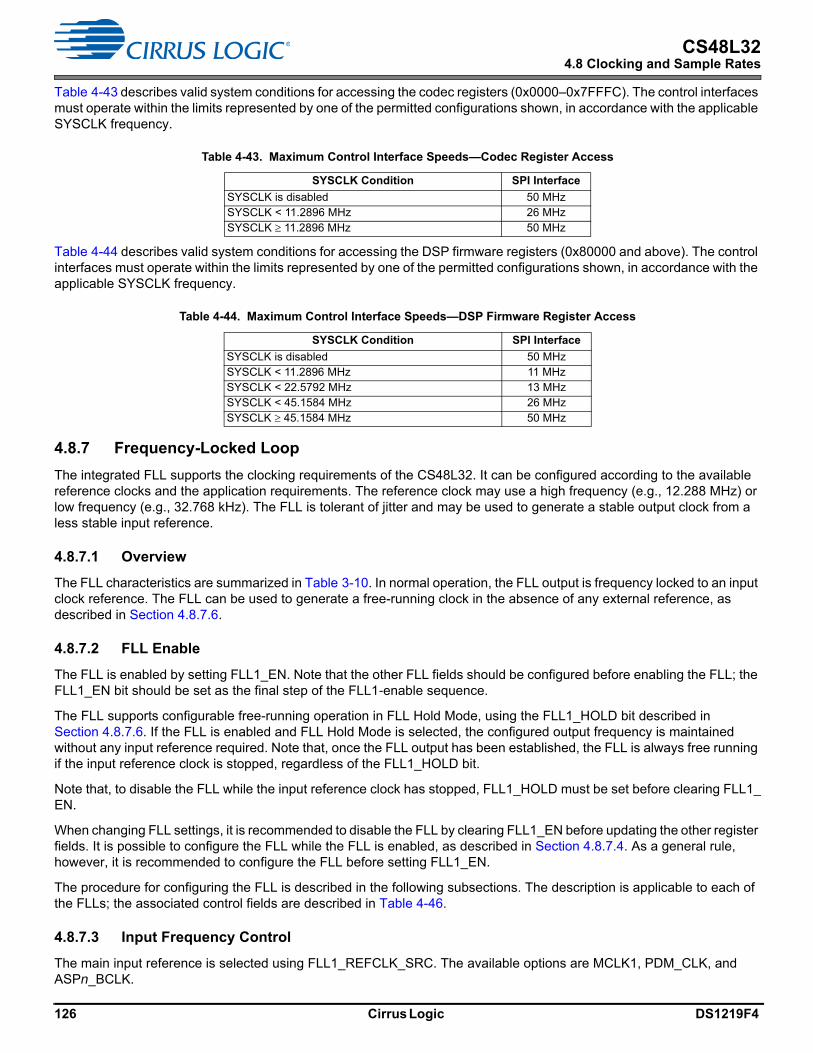
CS48L324.8 Clocking and Sample Rates
Table 4-43 describes valid system conditions for accessing the codec registers (0x0000–0x7FFFC). The control interfaces must operate within the limits represented by one of the permitted configurations shown, in accordance with the applicable SYSCLK frequency.
Table 4-44 describes valid system conditions for accessing the DSP firmware registers (0x80000 and above). The control interfaces must operate within the limits represented by one of the permitted configurations shown, in accordance with the applicable SYSCLK frequency.
4.8.7 Frequency-Locked Loop
The integrated FLL supports the clocking requirements of the CS48L32. It can be configured according to the available reference clocks and the application requirements. The reference clock may use a high frequency (e.g., 12.288 MHz) or low frequency (e.g., 32.768 kHz). The FLL is tolerant of jitter and may be used to generate a stable output clock from a less stable input reference.
4.8.7.1 Overview
The FLL characteristics are summarized in Table 3-10. In normal operation, the FLL output is frequency locked to an input clock reference. The FLL can be used to generate a free-running clock in the absence of any external reference, as described in Section 4.8.7.6.
4.8.7.2 FLL Enable
The FLL is enabled by setting FLL1_EN. Note that the other FLL fields should be configured before enabling the FLL; the FLL1_EN bit should be set as the final step of the FLL1-enable sequence.
The FLL supports configurable free-running operation in FLL Hold Mode, using the FLL1_HOLD bit described in Section 4.8.7.6. If the FLL is enabled and FLL Hold Mode is selected, the configured output frequency is maintained without any input reference required. Note that, once the FLL output has been established, the FLL is always free running if the input reference clock is stopped, regardless of the FLL1_HOLD bit.
Note that, to disable the FLL while the input reference clock has stopped, FLL1_HOLD must be set before clearing FLL1_EN.
When changing FLL settings, it is recommended to disable the FLL by clearing FLL1_EN before updating the other register fields. It is possible to configure the FLL while the FLL is enabled, as described in Section 4.8.7.4. As a general rule, however, it is recommended to configure the FLL before setting FLL1_EN.
The procedure for configuring the FLL is described in the following subsections. The description is applicable to each of the FLLs; the associated control fields are described in Table 4-46.
4.8.7.3 Input Frequency Control
The main input reference is selected using FLL1_REFCLK_SRC. The available options are MCLK1, PDM_CLK, and ASPn_BCLK.
Table 4-43. Maximum Control Interface Speeds—Codec Register Access
SYSCLK Condition SPI Interface
SYSCLK is disabled 50 MHzSYSCLK < 11.2896 MHz 26 MHzSYSCLK 11.2896 MHz 50 MHz
Table 4-44. Maximum Control Interface Speeds—DSP Firmware Register Access
SYSCLK Condition SPI Interface
SYSCLK is disabled 50 MHzSYSCLK < 11.2896 MHz 11 MHzSYSCLK < 22.5792 MHz 13 MHzSYSCLK < 45.1584 MHz 26 MHzSYSCLK 45.1584 MHz 50 MHz
126 Cirrus Logic DS1219F4

CS48L324.8 Clocking and Sample Rates
• The PDM_CLK reference can be derived from auxiliary PDM interfaces. The applicable source is selected using PDM_FLLCLK_SRC (see Table 4-8). Note that the PDM_CLK reference is only valid if the applicable PDM interface is operating in Slave Mode. See Section 4.2.10 for details of the auxiliary PDM interfaces.
The FLL1_REFCLK_DIV field controls a programmable divider on the selected input reference. The input can be divided by 1, 2, 4 or 8. The divider should be configured to bring the reference down to 13 MHz or below. For best performance, it is recommended that the highest possible frequency—within the 13 MHz limit—should be selected.
The FLL incorporates a reference-detection circuit for the main input clock. This ensures best FLL performance in the event of the main input clock being interrupted. If there is a possibility of the main input being interrupted while the FLL is enabled, then the reference-detection circuit must be enabled by setting FLL1_REFDET. The reference detection also provides input to the interrupt control circuit and can be used to trigger an interrupt event when the input reference is stopped—see Section 4.9.
4.8.7.4 Output Frequency Control
The FLL output frequency, FFLL, relative to the main input reference FREF, is a function of:
• The frequency ratio set by FLL1_FB_DIV
• The real number represented by N.K. (N = integer; K = fractional portion, i.e., < 1)
The output frequency must be in the range 45–50 MHz.
If the FLL is selected as SYSCLK source, the FFLL frequency must be exactly 49.152 MHz (for 48 kHz–related sample rates) or 45.1584 MHz (for 44.1 kHz–related sample rates).
If the FLL is selected as SYSCLK source, two different frequencies are available. Typical use cases should select the higher frequency (FFLL × 2); a lower frequency (FFLL) is available to support low-power always-on use cases.
The FLL clock can be used to provide a GPIO output (see Section 4.8.7.8); a programmable divider supports division ratios in the range 1–127, enabling a wide range of GPIO clock output frequencies.
To configure the FLL output frequency, it must be determined whether Integer Mode or Fractional Mode is required.
• If the ratio FFLL / FREF is an integer, then Integer Mode applies
• If the ratio FFLL / FREF is not an integer, then Fractional Mode applies
The input reference must be identified in one of three frequency ranges:
• If FREF < 192 kHz, this is low clock frequency
• If FREF 192 kHz and FREF < 1.152 MHz, this is mid clock frequency
• If FREF 1.152 MHz, this is high clock frequency
Note: FREF is the input frequency, after division by FLL1_REFCLK_DIV, where applicable.
The FLL output frequency, FFLL, is set according to the following equation:
FFLL = (FREF × N.K × FLL1_FB_DIV)
The FLL1_FB_DIV value should be configured according to the applicable mode and input reference frequency.
• If Integer Mode is used and FREF is low frequency, then FLL1_FB_DIV should be set to 4
• If Integer Mode is used and FREF is mid frequency, then FLL1_FB_DIV should be set to 2
• If Fractional Mode is used and FREF is low frequency, then FLL1_FB_DIV should be set to 256
• If Fractional Mode is used and FREF is mid frequency, then FLL1_FB_DIV should be set to 16
• Otherwise, FLL1_FB_DIV should be set to 1
The value of N.K can be determined as follows:
N.K = FFLL / (FLL1_FB_DIV × FREF)
DS1219F4 Cirrus Logic 127

CS48L324.8 Clocking and Sample Rates
The calculated value of N must lie within a valid range, according to the applicable mode.
• If Integer Mode is used, N is valid in the range 1–1023
• If Fractional Mode is used, N is valid in the range 2–255
If the calculated value of N is too high, a higher FLL1_FB_DIV is required. If the calculated value of N is too low, a lower FLL1_FB_DIV is required. It is recommended to adjust the FLL1_FB_DIV value by multiplying or dividing by 2 until a valid N is achieved.
The value of N is held in FLL1_N.
The value of K is determined by the ratio FLL1_THETA / FLL1_LAMBDA. In Fractional Mode, the FLL1_THETA and FLL1_LAMBDA fields can be derived as described in Section 4.8.7.5.
The FLL1_N, FLL1_THETA, and FLL1_LAMBDA fields are all coded as integers (LSB = 1).
When changing FLL settings, it is recommended to disable the FLL by clearing FLL1_EN before updating the other register fields. If the FLL settings or input reference are changed without disabling the FLL, the FLL Hold Mode must be selected before writing to any other FLL control fields. FLL Hold Mode is selected by setting FLL1_HOLD.
If the FLL control fields are written while the FLL is enabled (FLL1_EN = 1), the new values are only effective when a 1 is written to FLL1_CTRL_UPD. This makes it possible to update the FLL configuration fields simultaneously, without disabling the FLL.
To change FLL settings without disabling the FLL, the recommended control sequence is:
• Select FLL Hold Mode (FLL1_HOLD = 1)
• Write to the FLL control fields
• Update the FLL control registers (write 1 to FLL1_CTRL_UPD)
• Disable FLL Hold Mode (FLL1_HOLD = 0)
Note that, if the FLL is disabled, the FLL control fields can be updated without writing to FLL1_CTRL_UPD.
The FLL1_PD_GAIN_FINE, FLL1_PD_GAIN_COARSE, FLL1_FD_GAIN_FINE, FLL1_FD_GAIN_COARSE, and FLL1_HP fields should be configured as described in Table 4-45.
The FLL1_INTEG_DLY_MODE bit must be set (default) in all cases.
The FLL1_FB_DIV_SDM_ORD2_EN bit must be set in all cases.
Note: When writing to FLL1_FB_DIV_SDM_ORD2_EN, take care not to change other nonzero bits that are configured at the same register address.
4.8.7.5 Calculation of Theta and Lambda
In Fractional Mode, FLL1_THETA and FLL1_LAMBDA are calculated with the following steps:
Table 4-45. FLL Control Field Settings
ConditionFLL1_PD_GAIN_FINE
FLL1_PD_GAIN_COARSE
FLL1_FD_GAIN_FINE
FLL1_FD_GAIN_COARSE
FLL1_LOCKDET_THR
FLL1_HP
Low clock frequencyMid clock frequency
High clock frequency
0x20x20x2
0x30x20x1
0xF0xF0xF
0x00x20x0
0x20x80x8
—
Integer ModeFractional Mode
— — — — — 0x10x3
128 Cirrus Logic DS1219F4

CS48L324.8 Clocking and Sample Rates
1. Calculate GCD(FLL) using the Greatest Common Denominator function:
GCD(FLL) = GCD(FLL1_FB_DIV × FREF, FFLL),
where GCD(x, y) is the greatest common denominator of x and y.
FREF is the input frequency, after division by FLL1_REFCLK_DIV, where applicable.
2. Calculate FLL1_THETA and FLL1_LAMBDA using the following equations:
FLL1_THETA = (FFLL – (FLL1_N × FLL1_FB_DIV × FREF)) / GCD(FLL)
FLL1_LAMBDA = (FLL1_FB_DIV × FREF) / GCD(FLL)
Notes: The values of GCD(FLL), FLL1_THETA, and FLL1_LAMBDA should be calculated using the applicable frequencyvalues in Hz (i.e., not kHz or MHz).
In Fractional Mode, the values of FLL1_THETA and FLL1_LAMBDA must be coprime (i.e., not divisible by any common integer). The calculation above ensures that the values are coprime.
The value of K must be less than 1 (i.e., FLL1_THETA must be less than FLL1_LAMBDA).
4.8.7.6 FLL Hold Mode
FLL Hold Mode enables the FLL to generate a clock signal even if no external reference is available, such as when the normal input reference has been interrupted during a standby or start-up period. FLL Hold Mode is selected by setting FLL1_HOLD.
If the FLL is enabled and FLL Hold Mode is selected, the normal feedback mechanism of the FLL is halted and the FLL oscillates independently of the external input references—the FLL output frequency remains unchanged if FLL Hold Mode is enabled.
If the FLL is enabled and the input reference clock is stopped, the loop always runs freely, regardless of the FLL1_HOLD setting. If FLL1_HOLD = 0, the FLL relocks to the input reference whenever it is available.
If the FLL configuration or input reference are changed without disabling the FLL, the FLL Hold Mode must be selected before writing to any other FLL control fields—see Section 4.8.7.4.
The free-running FLL clock may be selected as the SYSCLK source, as shown in Fig. 4-52.
4.8.7.7 FLL Control Registers
The FLL1 control registers are described in Table 4-46.
Example settings for a variety of reference frequencies and output frequencies are shown in Section 4.8.7.10.
Table 4-46. FLL1 Register Map
Register Address Bit Label Default DescriptionR7168 (0x1C00)FLL1_CONTROL1
2 FLL1_CTRL_UPD 0 FLL1 Control UpdateWrite 1 to apply the FLL1 configuration field settings. (Only valid if FLL1_EN = 1)
1 FLL1_HOLD 1 FLL1 Hold Mode Enable0 = Disabled1 = EnabledThe FLL feedback mechanism is halted in FLL Hold Mode, and the latest integrator setting is maintained.
0 FLL1_EN 0 FLL1 Enable0 = Disabled1 = EnabledThis should be set as the final step of the FLL1 enable sequence.
DS1219F4 Cirrus Logic 129

CS48L324.8 Clocking and Sample Rates
R7172 (0x1C04)FLL1_CONTROL2
31:28 FLL1_LOCKDET_THR[3:0]
0x8 FLL1 Lock Detect thresholdValid from 0x0 (low threshold) to 0xF (high threshold)
27 FLL1_LOCKDET 1 FLL1 Lock Detect enabled0 = Disabled1 = Enabled
22 FLL1_PHASEDET 0 FLL1 Phase Detect control0 = Disabled1 = Enabled
21 FLL1_REFDET 1 FLL1 Reference Detect control0 = Disabled1 = Enabled
17:16 FLL1_REFCLK_DIV[1:0]
00 FLL1 Clock Reference divider00 = 101 = 2
10 = 411 = 8
MCLK (or other input reference) must be divided down to 13 MHz.15:12 FLL1_REFCLK_
SRC[3:0]0011 FLL1 Clock source
0000 = MCLK10011 = No input0101 = PDM_CLK
1000 = ASP1_BCLK1001 = ASP2_BCLKAll other codes are reserved
9:0 FLL1_N[9:0] 0x004 FLL1 Integer multiply for FREF
Coded as LSB = 1.R7176 (0x1C08)FLL1_CONTROL3
31:16 FLL1_LAMBDA[15:0]
0x0000 FLL1 Fractional multiply for FREF.Sets the denominator (dividing) part of the FLL1_THETA/FLL1_LAMBDA ratio.Coded as LSB = 1.
15:0 FLL1_THETA[15:0]
0x0000 FLL1 Fractional multiply for FREF.Sets the numerator (multiply) part of the FLL1_THETA/FLL1_LAMBDA ratio.Coded as LSB = 1.
Table 4-46. FLL1 Register Map (Cont.)
Register Address Bit Label Default Description
130 Cirrus Logic DS1219F4

CS48L324.8 Clocking and Sample Rates
4.8.7.8 FLL Interrupts and GPIO Output
The CS48L32 provides status signals that indicate whether the input reference is present and whether FLL lock has been achieved (i.e., the FLL is locked to the input reference signal).
To enable the FLL lock indication, the FLL1_LOCKDET bit must be set. The FLL lock condition is measured with respect to a configurable threshold that is set using FLL1_LOCKDET_THR. Note that the FLL1_LOCKDET_THR field controls the lock indication only—it does not control the behavior of the FLL.
To enable the FLL input reference indication, the FLL1_REFDET bit must be set.
The FLL status signals are inputs to the interrupt control circuit and can be used to trigger an interrupt event when the input reference is stopped or when the FLL lock status changes—see Section 4.9.
The FLL lock signal can be output directly on a GPIO pin as an external indication of the FLL status. See Section 4.10 to configure a GPIO pin for these functions.
R7180 (0x1C0C)FLL1_CONTROL4
31:28 FLL1_PD_GAIN_FINE[3:0]
0x2 FLL1 Phase Detector Gain 2Gain is 2–X, where X is FLL1_PD_GAIN_FINE in 2’s complement coding.0000 = 10001 = 0.50010 = 0.250011 = 0.1250100 = 2–4
0101 = 2–5
0110 = 2–6
0111 = 2–7
1000 = 2561001 = 1281010 = 641011 = 32
1100 = 161101 = 81110 = 41111 = 2
27:24 FLL1_PD_GAIN_COARSE[3:0]
0x1 FLL1 Phase Detector Gain 1Gain is 2–X, where X is FLL1_PD_GAIN_COARSE in 2’s complement coding.0000 = 10001 = 0.50010 = 0.250011 = 0.1250100 = 2–4
0101 = 2–5
0110 = 2–6
0111 = 2–7
1000 = 2561001 = 1281010 = 641011 = 32
1100 = 161101 = 81110 = 41111 = 2
23:20 FLL1_FD_GAIN_FINE[3:0]
0xF FLL1 Frequency Detector Gain 2Gain is 2–X, where X is FLL1_FD_GAIN_FINE in integer coding.0000 = 10001 = 0.50010 = 0.25
0011 = 0.125...1101 = 2–13
1110 = 2–14
1111 = Disabled
19:16 FLL1_FD_GAIN_COARSE[3:0]
0x0 FLL1 Frequency Detector Gain 1Gain is 2–X, where X is FLL1_FD_GAIN_COARSE in 2’s complement coding.0000 = 10001 = 0.50010 = 0.250011 = 0.1250100 = 2–4
0101 = 2–5
0110 = 2–6
0111 = 2–7
1000 = 2561001 = 1281010 = 641011 = 32
1100 = 161101 = 81110 = 41111 = 2
14 FLL1_INTEG_DLY_MODE
1 FLL1 Integrator Delay controlThis bit should be set at all times.
13:12 FLL1_HP[1:0] 01 FLL1 Fractional Mode control00 = Reserved01 = Integer Mode
10 = Reserved11 = Fractional Mode
9:0 FLL1_FB_DIV[9:0] 0x001 FLL1 Clock Feedback ratioCoded as LSB = 1.
R7220 (0x1C34)FLL1_DIGITAL_TEST2
10 FLL1_FB_DIV_SDM_ORD2_EN
0 FLL1 Fractional divider control0 = Disabled, 1 = EnabledThis bit should be set at all times.
Table 4-46. FLL1 Register Map (Cont.)
Register Address Bit Label Default Description
DS1219F4 Cirrus Logic 131

CS48L324.8 Clocking and Sample Rates
Clock output signals derived from the FLL can be output on a GPIO pin. See Section 4.10 to configure a GPIO pin for this function.
4.8.7.9 Example FLL Calculation
The following example illustrates how to derive the FLL1 register fields to generate an FLL output frequency (FFLL) of 49.152 MHz from a 12.000 MHz reference clock (FREF). This is suitable for generating SYSCLK at 98.304 MHz.
1. Set FLL1_REFCLK_DIV to generate FREF 13 MHz:
FLL1_REFCLK_DIV = 00 (divide by 1)
2. Determine if Integer Mode or Fractional Mode is required:
FFLL / FREF is 4.096. Therefore, Fractional Mode applies.
3. Identify the input clock frequency range:
FREF 1.152 MHz. This is high clock frequency.
4. Select the required value of FLL1_FB_DIV:
In Fractional Mode, with high clock frequency input, FLL1_FB_DIV = 1
5. Calculate N.K as given by N.K = FFLL / (FLL1_FB_DIV × FREF):
N.K = 49152000 / (1 × 12000000) = 4.096
6. Confirm that the calculated value of N is within the valid range for fractional mode (2–255).
7. Determine FLL1_N from the integer portion of N.K:
FLL1_N = 4 (0x004)
8. Determine GCD(FLL), as given by GCD(FLL) = GCD(FLL1_FB_DIV × FREF, FFLL):
GCD(FLL) = GCD(1 × 12000000, 49152000) = 96000
9. Determine FLL1_THETA, as given by FLL1_THETA = (FFLL – (FLL1_N × FLL1_FB_DIV × FREF)) / GCD(FLL):
FLL1_THETA = (49152000 – (4 × 1 × 12000000)) / 96000FLL1_THETA = 12 (0x000C)
10.Determine FLL1_LAMBDA, as given by FLL1_LAMBDA = (FLL1_FB_DIV x FREF) / GCD(FLL):
FLL1_LAMBDA = (1 × 12000000) / 96000FLL1_LAMBDA = 125 (0x007D)
11.Determine other FLL settings (see Table 4-45) for Fractional Mode and high clock-frequency input:
FLL1_PD_GAIN_FINE = 0x2FLL1_PD_GAIN_COARSE = 0x1FLL1_FD_GAIN_FINE = 0xFFLL1_FD_GAIN_COARSE = 0x0FLL1_HP = 0x3FLL1_INTEG_DLY_MODE = 1FLL1_FB_DIV_SDM_ORD2_EN = 1
4.8.7.10 Example FLL Settings
Table 4-47 shows FLL settings for generating an output frequency (FFLL) of 49.152 MHz from a variety of low- and high-frequency reference inputs. This is suitable for generating SYSCLK at 98.304 MHz.
Note that FLL1_INTEG_DLY_MODE, FLL1_FB_DIV_SDN_ORD2_EN, and other fields referenced in Table 4-45 must also be configured according to the required FLL operation.
132 Cirrus Logic DS1219F4

CS48L324.9 Interrupts
4.9 Interrupts
The interrupt controller has multiple inputs. These include the GPIO input pins, FLL-lock detection, and status flags from DSP peripheral functions. See Table 4-48 for a full definition of the interrupt controller inputs. Any combination of these inputs can be used to trigger an interrupt request event.
An interrupt register field is associated with each interrupt input. All interrupts support edge-sensitive triggering (i.e., the interrupt is asserted when a logic edge is detected on the respective input). Some interrupts are triggered on rising edges of the respective input only; for others, separate rising- and falling-edge interrupts are provided. The interrupt register fields can be polled at any time or in response to the interrupt request output being signaled via the IRQ pin or a GPIO pin.
The interrupt-status fields indicate the current value of the corresponding inputs to the interrupt controller. Note that the status of any GPIO (or DSP GPIO) inputs can also be read using the GPIO (or DSP GPIO) control fields, as described in Table 4-49 and Table 4-33.
Mask bits are provided for each interrupt signal, to enable or disable the respective functions from the IRQ output. Note that the interrupt register fields remain valid—even if masked—but the masked interrupts do not cause the IRQ output to be asserted.
The interrupt-request output represents the logical OR of all the unmasked interrupt registers. The interrupt register fields are latching fields and, once they are set, they are not reset until a 1 is written to the respective bits. The interrupt request outputs are not reset until each of the associated interrupts has been reset.
The GPIO interrupts can be configured for edge- or level-triggered behavior using the respective GPIOn_FALL_EDGE1 and GPIOn_RISE_EDGE1 fields. A debounce circuit can be enabled on the GPIO inputs, to avoid false event triggers; this is enabled on each pin using the fields described in Table 4-49. The GPIO debounce circuit uses the 32 kHz clock, which must be enabled whenever the GPIO debounce function is required.
The IRQ output can be globally masked using IRQ1_MASK. The IRQ status can be read from IRQ1_STS—note that this bit is not affected by IRQ1_MASK.
The IRQ1 output is provided externally on the IRQ pin. Under default conditions, this output is active low. The polarity can be inverted using IRQ_POL. The IRQ pin can be configured as a CMOS-driven or open-drain output using IRQ_OP_CFG. The IRQ output is referenced to the VDD_IO power domain.
The IRQ1 signal can also be output on a GPIO pin—see Section 4.10. Note that the GPIO output is not affected by IRQ_POL; the polarity can, instead, be selected using the GPIO control fields.
Table 4-47. Example FLL Settings
FSOURCE FFLL (MHz) FREF Divider1
1.See Table 4-46 for the coding of the FLL1_REFCLK_DIV and FLL1_FB_DIV fields.
FB_DIV1 N.K 2
2.N.K values are represented in the FLL1_N, FLL1_THETA, and FLL1_LAMBDA fields.
FLL1_NFLL1_THETA
FLL1_LAMBDA
32.000 kHz 49.152 1 4 384 0x180 0x0000 0x000132.768 kHz 49.152 1 4 375 0x177 0x0000 0x000144.100 kHz 49.152 1 256 4.3537415 0x004 0x0034 0x009348 kHz 49.152 1 4 256 0x100 0x0000 0x0001128 kHz 49.152 1 4 96 0x060 0x0000 0x00019.6 MHz 49.152 1 1 5.12 0x005 0x0003 0x001910 MHz 49.152 1 1 4.9152 0x004 0x023C 0x027111.2896 MHz 49.152 1 1 4.3537415 0x004 0x0034 0x009312.000 MHz 49.152 1 1 4.096 0x004 0x000C 0x007D12.288 MHz 49.152 1 1 4 0x004 0x0000 0x000113.000 MHz 49.152 1 1 3.7809231 0x003 0x04F5 0x065919.200 MHz 49.152 2 1 5.12 0x005 0x0003 0x001922.5792 MHz 49.152 2 1 4.3537415 0x004 0x0034 0x009324 MHz 49.152 2 1 4.096 0x004 0x000C 0x007D24.576 MHz 49.152 2 1 4 0x004 0x0000 0x000126 MHz 49.152 2 1 3.7809231 0x003 0x04F5 0x0659
DS1219F4 Cirrus Logic 133

CS48L324.9 Interrupts
The CS48L32 interrupt controller circuit is shown in Fig. 4-54. (Note that not all interrupt inputs are shown.) The control fields associated with IRQ1 are described in Table 4-48. Note that, under default register conditions, the boot done status is the only unmasked interrupt source; a falling edge on the IRQ pin indicates completion of the boot sequence.
Figure 4-54. Interrupt Controller
The IRQ1 control registers are described in Table 4-48.
Table 4-48. Interrupt 1 Control Registers
Register Address Bit Label Default DescriptionR10000 (0x2710)IRQ1_CTRL_AOD
11 IRQ1_MASK 0 IRQ1 output interrupt mask.0 = Do not mask interrupt.1 = Mask interrupt.
10 IRQ_POL 1 IRQ output polarity select0 = Noninverted (active high)1 = Inverted (active low)
9 IRQ_OP_CFG 1 IRQ output configuration0 = CMOS1 = Open drain
R98308 (0x18004)IRQ1_STATUS
0 IRQ1_STS 0 IRQ1 statusLogical OR of all unmasked x_EINT1 interrupts.0 = Not asserted1 = AssertedThis bit is valid regardless of IRQ1_MASK
R98320 (0x18010)IRQ1_EINT_1
10 SYSCLK_ERR_EINT1 0 SYSCLK Error Interrupt (Rising edge triggered)8 SYSCLK_FAIL_EINT1 0 SYSCLK Fail Interrupt (Rising edge triggered)
R98324 (0x18014)IRQ1_EINT_2
3 BOOT_DONE_EINT1 0 Boot Done Interrupt (Rising edge triggered)
R98336 (0x18020)IRQ1_EINT_5
25 US2_SIG_DET_FALL_EINT1 0 US2 Ultrasonic Signal-Detect Interrupt (Falling edge triggered)
24 US2_SIG_DET_RISE_EINT1 0 US2 Ultrasonic Signal-Detect Interrupt (Rising edge triggered)
23 US1_SIG_DET_FALL_EINT1 0 US1 Ultrasonic Signal-Detect Interrupt (Falling edge triggered)
22 US1_SIG_DET_RISE_EINT1 0 US1 Ultrasonic Signal-Detect Interrupt (Rising edge triggered)
21 INPUTS_SIG_DET_FALL_EINT1 0 Input Path Signal-Detect Interrupt (Falling edge triggered)20 INPUTS_SIG_DET_RISE_EINT1 0 Input Path Signal-Detect Interrupt (Rising edge triggered)19 DRC2_SIG_DET_FALL_EINT1 0 DRC2 Signal-Detect Interrupt (Falling edge triggered)18 DRC2_SIG_DET_RISE_EINT1 0 DRC2 Signal-Detect Interrupt (Rising edge triggered)17 DRC1_SIG_DET_FALL_EINT1 0 DRC1 Signal-Detect Interrupt (Falling edge triggered)16 DRC1_SIG_DET_RISE_EINT1 0 DRC1 Signal-Detect Interrupt (Rising edge triggered)
xxx_STS1
EVENT1_FULL_STS1
FLL1_LOCK_STS1
DRC1_SIG_DET_STS1
xxx_STS1
xxx_MASK1
EVENT1_FULL_MASK1
FLL1_LOCK_RISE_MASK1
FLL1_LOCK_FALL_MASK1
DRC1_SIG_DET_RISE_MASK1
DRC1_SIG_DET_FALL_MASK1
xxx_MASK1xxx_EINT1
EVENT1_FULL_EINT1
FLL1_LOCK_RISE_EINT1
FLL1_LOCK_FALL_EINT1
DRC1_SIG_DET_RISE_EINT1
DRC1_SIG_DET_FALL_EINT1
xxx_EINT1
IRQ1_MASK
IRQ1_STS
IRQ_POL
GPIO
IRQ pin
Edg
e de
tect
ion
Note: Not all available interrupt sources are shown.
134 Cirrus Logic DS1219F4

CS48L324.9 Interrupts
R98340 (0x18024)IRQ1_EINT_6
8 FLL1_REF_LOST_EINT1 0 FLL1 Reference Lost Interrupt (Rising edge triggered)1 FLL1_LOCK_FALL_EINT1 0 FLL1 Lock Interrupt (Falling edge triggered)0 FLL1_LOCK_RISE_EINT1 0 FLL1 Lock Interrupt (Rising edge triggered)
R98344 (0x18028)IRQ1_EINT_7
21 DSP1_MPU_ERR_EINT1 0 DSP1 memory protection error (rising-edge triggered)20 DSP1_WDT_EXPIRE_EINT1 0 DSP1 watchdog timer expiry (rising-edge triggered)19 DSP1_IHB_ERR_EINT1 0 DSP1 memory controller error (rising-edge triggered)18 DSP1_AHB_SYS_ERR_EINT1 0 DSP1 AHB system error (rising-edge triggered)17 DSP1_AHB_PACK_ERR_EINT1 0 DSP1 AHB packing error (rising-edge triggered)16 DSP1_NMI_ERR_EINT1 0 DSP1 NMI error (rising-edge triggered)
R98352 (0x18030)IRQ1_EINT_9
31 MCU_HWERR_IRQ_OUT_EINT1 0 Memory control error (rising-edge triggered)3 DSP1_IRQ3_EINT1 0 DSP1 IRQ3 interrupt (rising-edge triggered)2 DSP1_IRQ2_EINT1 0 DSP1 IRQ2 interrupt (rising-edge triggered)1 DSP1_IRQ1_EINT1 0 DSP1 IRQ1 interrupt (rising-edge triggered)0 DSP1_IRQ0_EINT1 0 DSP1 IRQ0 interrupt (rising-edge triggered)
R98360 (0x18038)IRQ1_EINT_11
31 GPIO8_FALL_EINT1 0 GPIO8 Interrupt (Falling edge triggered)30 GPIO8_RISE_EINT1 0 GPIO7 Interrupt (Rising edge triggered)29 GPIO7_FALL_EINT1 0 GPIO6 Interrupt (Falling edge triggered)28 GPIO7_RISE_EINT1 0 GPIO5 Interrupt (Rising edge triggered)27 GPIO6_FALL_EINT1 0 GPIO4 Interrupt (Falling edge triggered)26 GPIO6_RISE_EINT1 0 GPIO3 Interrupt (Rising edge triggered)25 GPIO5_FALL_EINT1 0 GPIO2 Interrupt (Falling edge triggered)24 GPIO5_RISE_EINT1 0 GPIO1 Interrupt (Rising edge triggered)23 GPIO4_FALL_EINT1 0 GPIO8 Interrupt (Falling edge triggered)22 GPIO4_RISE_EINT1 0 GPIO7 Interrupt (Rising edge triggered)21 GPIO3_FALL_EINT1 0 GPIO6 Interrupt (Falling edge triggered)20 GPIO3_RISE_EINT1 0 GPIO5 Interrupt (Rising edge triggered)19 GPIO2_FALL_EINT1 0 GPIO4 Interrupt (Falling edge triggered)18 GPIO2_RISE_EINT1 0 GPIO3 Interrupt (Rising edge triggered)17 GPIO1_FALL_EINT1 0 GPIO2 Interrupt (Falling edge triggered)16 GPIO1_RISE_EINT1 0 GPIO1 Interrupt (Rising edge triggered)
R98364 (0x1803C)IRQ1_EINT_12
16 EVENT1_FULL_EINT1 0 Event Log 1 FIFO Full Interrupt (Rising edge triggered)
R98368 (0x18040)IRQ1_EINT_13
3 DSP1_TRB_STACK_ERR_EINT1 0 DSP1 trace buffer stack interrupt (rising-edge triggered)1 DSP1_MIPS_PROF1_DONE_EINT1 0 DSP1 MIPS profile 1 done interrupt (rising-edge triggered)0 DSP1_MIPS_PROF0_DONE_EINT1 0 DSP1 MIPS profile 0 done interrupt (rising-edge triggered)
R98376 (0x18048)IRQ1_EINT_15
3 SPI2_STALLING_EINT1 0 SPI2 Stall Interrupt (Rising edge triggered)2 SPI2_BLOCK_EINT1 0 SPI2 Block Interrupt (Rising edge triggered)0 SPI2_DONE_EINT1 0 SPI2 Done Interrupt (Rising edge triggered)
R98384 (0x18050)IRQ1_EINT_17
17 TIMER2_EINT1 0 Timer 1 Interrupt (Rising edge triggered)16 TIMER1_EINT1 0 Timer 1 Interrupt (Rising edge triggered)
R98388 (0x18054)IRQ1_EINT_18
3 TIMER_ALM1_CH4_EINT1 0 Alarm 1 Channel 4 Interrupt (Rising edge triggered)2 TIMER_ALM1_CH3_EINT1 0 Alarm 1 Channel 3 Interrupt (Rising edge triggered)1 TIMER_ALM1_CH2_EINT1 0 Alarm 1 Channel 2 Interrupt (Rising edge triggered)0 TIMER_ALM1_CH1_EINT1 0 Alarm 1 Channel 1 Interrupt (Rising edge triggered)
R98448 (0x18090)IRQ1_STS_1
10 SYSCLK_ERR_STS1 0 SYSCLK error interrupt status0 = Normal, 1 = Insufficient SYSCLK cycles for the requested signal path functionality
R98452 (0x18094)IRQ1_STS_2
3 BOOT_DONE_STS1 0 Boot Status0 = Busy (boot sequence in progress)1 = Idle (boot sequence completed)Control register writes should not be attempted until Boot Sequence has completed.
Table 4-48. Interrupt 1 Control Registers (Cont.)
Register Address Bit Label Default Description
DS1219F4 Cirrus Logic 135

CS48L324.9 Interrupts
R98464 (0x180A0)IRQ1_STS_5
24 US2_SIG_DET_STS1 0 US2 ultrasonic signal-detect status0 = Normal, 1 = Signal detected
22 US1_SIG_DET_STS1 0 US1 ultrasonic signal-detect status0 = Normal, 1 = Signal detected
20 INPUTS_SIG_DET_STS1 0 Input path signal-detect status0 = Normal, 1 = Signal detected
18 DRC2_SIG_DET_STS1 0 DRC2 signal-detect status0 = Normal, 1 = Signal detected
16 DRC1_SIG_DET_STS1 0 DRC1 signal-detect status0 = Normal, 1 = Signal detected
R98468 (0x180A4)IRQ1_STS_6
8 FLL1_REF_LOST_STS1 0 FLL1 reference-lost status0 = Normal, 1 = Reference lost
0 FLL1_LOCK_STS1 0 FLL1 lock status0 = Not locked, 1 = Locked
R98472 (0x180A8)IRQ1_STS_7
20 DSP1_WDT_EXPIRE_STS1 DSP1 watchdog timer status0 = Normal, 1 = Watchdog timer expired
18 DSP1_AHB_SYS_ERR_STS1 DSP1 AHB system status0 = Normal, 1 = Error
17 DSP1_AHB_PACK_ERR_STS1 DSP1 AHB packing status0 = Normal, 1 = Error
16 DSP1_NMI_ERR_STS1 DSP1 NMI status0 = Normal, 1 = NMI asserted
R98480 (0x180B0)IRQ1_STS_9
3 DSP1_IRQ3_STS1 0 DSP1 IRQ3 status0 = Normal, 1 = Interrupt asserted
2 DSP1_IRQ2_STS1 0 DSP1 IRQ2 status0 = Normal, 1 = Interrupt asserted
1 DSP1_IRQ1_STS1 0 DSP1 IRQ1 status0 = Normal, 1 = Interrupt asserted
0 DSP1_IRQ0_STS1 0 DSP1 IRQ0 status0 = Normal, 1 = Interrupt asserted
R98488 (0x180B8)IRQ1_STS_11
30 GPIO8_STS1 0 GPIOn input status. Reads back the logic level of GPIOn.Only valid for pins configured as GPIO input (does not include DSPGPIO inputs).
28 GPIO7_STS1 026 GPIO6_STS1 024 GPIO5_STS1 022 GPIO4_STS1 020 GPIO3_STS1 018 GPIO2_STS1 016 GPIO1_STS1 0
R98492 (0x180BC)IRQ1_STS_12
16 EVENT1_FULL_STS1 0 Event Log 1 FIFO Full status0 = FIFO Not Full, 1 = FIFO Full
R98576 (0x18110)toR98644 (0x18154)
x_MASK1 See Footnote 1
For each x_EINT1 interrupt bit in registers 0x18010–0x18054, a corresponding mask bit (x_MASK1) is provided in registers 0x18110–0x18154.The mask bits are coded as follows:0 = Do not mask interrupt1 = Mask interrupt
Table 4-48. Interrupt 1 Control Registers (Cont.)
Register Address Bit Label Default Description
136 Cirrus Logic DS1219F4

CS48L324.10 General-Purpose I/O
4.10 General-Purpose I/O
The CS48L32 supports up to 16 GPIO pins, which can be assigned to application-specific functions. The GPIOs enable interfacing and detection of external hardware and can provide logic outputs to other devices. The GPIO input functions can be used to generate an interrupt (IRQ) event.
There are two dedicated GPIO pins; the remaining GPIOs are implemented as alternate functions to a pin-specific capability. The GPIO and interrupt circuits support the following functions:
• Pin-specific alternative functions for external interfaces (ASP, PDM, SPI2)
• Logic input/button detect (GPIO input)
• Logic 1 and Logic 0 output (GPIO output)
• Interrupt (IRQ) status
• Clock output
• Frequency-locked loop (FLL) status
• FLL clock output
• Pulse-width modulation (PWM) signal output
• Input signal-detection status
• Alarm generator output
• General-purpose timer status
• DSP busy/idle status
• SPI master interface
Logic input and output (GPIO) can be supported in two different ways on the CS48L32. The standard mechanism described in this section provides a comprehensive suite of options including input debounce, and selectable output drive configuration. The DSP GPIO circuit is tailored towards more advanced requirements typically demanded by DSP software features. The DSP GPIO functions are described in Section 4.5.4.
4.10.1 GPIO Control
For each GPIO, the selected function is determined by the GPn_FN field, where n identifies the GPIO pin (1–16). The pin direction, set by GPn_DIR, must be set according to function selected by GPn_FN.
If a pin is configured as a GPIO input (GPn_DIR = 1, GPn_FN = 0x001), the logic level at the pin can be read from the respective GPn_STS bit. Note that GPn_STS is not affected by the polarity-select (GPn_POL) bit.
R98872 (0x18238)IRQ1_EDGE_11
31 GPIO8_FALL_EDGE1 0 GPIOn interrupt type0 = Level-triggered1 = Edge-triggered
30 GPIO8_RISE_EDGE1 029 GPIO7_FALL_EDGE1 028 GPIO7_RISE_EDGE1 027 GPIO6_FALL_EDGE1 026 GPIO6_RISE_EDGE1 025 GPIO5_FALL_EDGE1 024 GPIO5_RISE_EDGE1 023 GPIO4_FALL_EDGE1 022 GPIO4_RISE_EDGE1 021 GPIO3_FALL_EDGE1 020 GPIO3_RISE_EDGE1 019 GPIO2_FALL_EDGE1 018 GPIO2_RISE_EDGE1 017 GPIO1_FALL_EDGE1 016 GPIO1_RISE_EDGE1 0
1.The BOOT_DONE_EINT1 interrupt is 0 (unmasked) by default; all other interrupts are 1 (masked) by default.
Table 4-48. Interrupt 1 Control Registers (Cont.)
Register Address Bit Label Default Description
DS1219F4 Cirrus Logic 137

CS48L324.10 General-Purpose I/O
A debounce circuit can be enabled on any GPIO input, to avoid false event triggers. This is enabled on each pin by setting the respective GPn_DB bit. The debounce circuit uses the 32 kHz clock, which must be enabled whenever input debounce functions are required. The debounce time is configurable for each GPIO using GPn_DBTIME. See Section 4.8 for further details of the CS48L32 clocking configuration.
Each GPIO pin is an input to the interrupt control circuit and can be used to trigger an interrupt event. An interrupt event is triggered on the rising and falling edges of the GPIO input. The associated interrupt bit is latched once set; it can be polled at any time or used to control the IRQ signal. See Section 4.9 for details of the interrupt event handling.
Integrated pull-up and pull-down resistors are provided on each GPIO pin; these can be configured independently using the GPn_PU and GPn_PD fields. When the pull-up and pull-down control bits are both enabled, the CS48L32 provides a bus keeper function on the respective pin. The bus keeper function holds the logic level unchanged whenever the pin is undriven (e.g., if the signal is tristated).
Note: The bus keeper is enabled by default on all GPIO pins and, if not actively driven, may result in either a Logic 0 or Logic 1 at the respective input on start-up. If an external pull resistor is connected, the chosen resistance should take account of the bus keeper resistance (see Table 3-9). A strong pull resistor (e.g., 10 k) is required, if a specific start-up condition is to be forced by the external pull component.
If a pin is configured as a GPIO output (GPn_DIR = 0, GPn_FN = 0x001), its level can be set to Logic 0 or Logic 1 using the GPn_LVL field. Note that the GPn_LVL bits are write-only—they do not provide status indication of GPIO input or output levels.
If a pin is configured as an output (GPn_DIR = 0), the polarity can be selected using GPn_POL. If GPn_POL = 1, the selected output function is inverted. Note that, if GPn_FN = 0x000 or 0x002, the GPn_POL bit has no effect on the respective GPIO pin.
A GPIO output can be either CMOS driven or open drain. This is selected on each pin using the respective GPn_OP_CFG bit. Note that if GPn_FN = 0x000 the GPn_OP_CFG bit has no effect on the respective GPIO pin—see Table 4-49 for further details. If GPn_FN = 0x002, the respective pin output is CMOS.
The output drive strength of GPIOs is selectable using the respective GPn_DRV_STR bits.
The register fields that control the GPIO pins are described in Table 4-49.
Table 4-49. GPIO Control
Register Address Bit Label Default DescriptionR3072 (0x0C00)GPIO_STATUS1
15 GP16_STS 0 GPIOn input level. Read this bit to read GPIO input level.14 GP15_STS 013 GP14_STS 012 GP13_STS 011 GP12_STS 010 GP11_STS 09 GP10_STS 08 GP9_STS 07 GP8_STS 06 GP7_STS 05 GP6_STS 04 GP5_STS 03 GP4_STS 02 GP3_STS 01 GP2_STS 00 GP1_STS 0
138 Cirrus Logic DS1219F4

CS48L324.10 General-Purpose I/O
4.10.2 GPIO Function Select
The available GPIO functions are described in Table 4-50. The function of each GPIO is set using GPn_FN, where n identifies the GPIO pin (1–16). Note that the respective GPn_DIR must also be set according to whether the function is an input or output.
R3080 (0x0C08)GPIO1_CTRL1toR3140 (0x0C44)GPIO16_CTRL1
31 GPn_DIR 1 GPIOn pin direction0 = Output1 = InputNote that, if GPn_FN = 0x000 or 0x002, this bit has no effect on the GPIOn pin. If GPn_FN = 0x000, the pin direction is set according to the applicable pin-specific function (see Table 4-51). If GPn_FN = 0x002, the pin direction is set according to the DSP GPIO configuration.
30 GPn_PU 1 GPIOn pull-up enable0 = Disabled1 = EnabledNote: If GPn_PD and GPn_PU are both set, a bus keeper function is enabled on the respective GPIOn pin.
29 GPn_PD 1 GPIOn pull-down enable0 = Disabled1 = EnabledNote: If GPn_PD and GPn_PU are both set, a bus keeper function is enabled on the respective GPIOn pin.
24 GPn_DRV_STR 1 GPIOn output drive strength0 = 4 mA1 = 8 mA
19:16 GPn_DBTIME[3:0] 0x0 GPIOn input debounce time0x0 = 100 s0x1 = 1.5 ms0x2 = 3 ms
0x3 = 6 ms0x4 = 12 ms0x5 = 24 ms
0x6 = 48 ms0x7 = 96 ms0x8 = 192 ms
0x9 = 384 ms0xA = 768 ms0xB–0xF = Reserved
15 GPn_LVL See Footnote 2
GPIOn level (write-only). Write to this bit to set a GPIO output.If GPn_POL is set, the GPn_LVL bit is the opposite logic level to the external pin.
14 GPn_OP_CFG 0 GPIOn output configuration0 = CMOS1 = Open drainNote that, if GPn_FN = 0x000 or 0x002, this bit has no effect on the GPIOn output. If GPn_FN = 0x000, the pin configuration is set according to the applicable pin-specific function (see Table 4-51). If GPn_FN = 0x002, the pin configuration is CMOS.
13 GPn_DB 0 GPIOn input debounce select0 = Disabled1 = Enabled
12 GPn_POL 0 GPIOn output polarity0 = Noninverted (Active High)1 = Inverted (Active Low)Note that, if GPn_FN = 0x000 or 0x002, this bit has no effect on the GPIOn output.
9:0 GPn_FN[9:0] 0x001 GPIOn Pin Function(see Table 4-50 for details)
1. n is a number (1–16) that identifies the individual GPIO.2. The default value of GPn_LVL depends upon whether the pin is actively driven by another device. If the pin is actively driven, the bus keeper
maintains this logic level. If the pin is not actively driven, the bus keeper may establish either a Logic 1 or Logic 0 as the initial input level.
Table 4-49. GPIO Control (Cont.)
Register Address Bit Label Default Description
DS1219F4 Cirrus Logic 139

CS48L324.10 General-Purpose I/O
4.10.3 Pin-Specific Alternate Function—GPn_FN = 0x000
The CS48L32 provides two dedicated GPIO pins (GPIO1, GPIO2). The remaining GPIOs are multiplexed with the pin-specific functions listed in Table 4-51. The alternate functions are selected by setting the respective GPn_FN fields to 0x000, as described in Section 4.10.1. Note that each function is unique to the associated pin and can be supported only on that pin.
If the alternate function is selected on a GPIO pin, the pin direction (input or output) and the output driver configuration (CMOS or open drain) are set as described in Table 4-51. The respective GPn_DIR and GPn_OP_CFG bits have no effect in this case.
Table 4-50. GPIO Function Select
GPn_FN Valid On Description Comments0x000 All GPIOs (1–16) Pin-specific alternate function Alternate configuration supporting ASPn and SPI2 interface functions.0x001 All GPIOs (1–16) Button-detect input/logic-level output GPn_DIR = 0: GPIO pin logic level is set by GPn_LVL.
GPn_DIR = 1: Button detect or logic level input.0x002 All GPIOs (1–16) DSP GPIO Low latency input/output for DSP functions.0x003 GPIO1–8 only IRQ1 output Interrupt (IRQ1) output
0 = IRQ1 not asserted1 = IRQ1 asserted
0x010 GPIO1–8 only FLL1 clock Clock output from FLL10x018 GPIO1–8 only FLL1 lock Indicates FLL1 lock status
0 = Not locked1 = Locked
0x048 GPIO1–8 only OPCLK clock output Configurable clock output derived from SYSCLK0x080 All GPIOs (1–16) PWM1 output Configurable PWM output PWM10x081 All GPIOs (1–16) PWM2 output Configurable PWM output PWM20x08C GPIO1–8 only Input signal path signal detect Indicates inputs signal path signal detect status
0 = Signal threshold not exceeded1 = Signal threshold exceeded
0x090 GPIO1–8 only US1 ultrasonic signal detect Indicates US1 ultrasonic signal-detect status0 = Signal threshold not exceeded1 = Signal threshold exceeded
0x092 GPIO1–8 only US2 ultrasonic signal detect Indicates US2 ultrasonic signal-detect status0 = Signal threshold not exceeded1 = Signal threshold exceeded
0x158 GPIO1–8 only Event Log 1 FIFO not-empty status Event Log 1 FIFO not-empty status0 = FIFO empty1 = FIFO not empty
0x230–0x233
All GPIOs (1–16) Alarm 1 Channel n status Alarm 1 Channel n status (n is 1–4)A pulse is output when the respective alarm-trigger conditions are met. The pulse duration is configurable.
0x250 All GPIOs (1–16) Timer 1 status Timer 1 statusA pulse is output after the respective timer reaches its final count value.
0x251 All GPIOs (1–16) Timer 2 status Timer 2 statusA pulse is output after the respective timer reaches its final count value.
0x373 GPIO1–8 only DSP1 power status DSP1 power status0 = Busy1 = Idle
0x608–0x60B
GPIO1–10 only SPI2 Slave Select 1–4 Slave-select outputs controlled by the SPI2 master interface
140 Cirrus Logic DS1219F4

CS48L324.10 General-Purpose I/O
4.10.4 Button Detect input/Logic Level output—GPn_FN = 0x001
The GPIO pins can be configured for general-purpose digital input/output by setting the respective GPIO fields as described in Section 4.10.1.
• The GPIO input configuration is suitable for button-detect functionality. Note that it is recommended to enable the GPIO input debounce feature when using GPIOs as button input.
The GPn_STS fields indicate the logic levels on each GPIO input—after the respective debounce function. Note that GPn_STS is not affected by the GPn_POL bit.
The debounced GPIO signals are also inputs to the interrupt-control circuit. Separate interrupts are associated with the rising and falling edges of the GPIO input. The associated interrupt bits are latched once set; they can be polled at any time or used to control the IRQ signal. See Section 4.9 for details of the interrupt event handling.
• The GPIO output can be used to drive a logic high or logic low level to provide an indication or control signal to an external circuit.
The output logic level is selected using the respective GPn_LVL bit. Note that the GPn_LVL bits are write-only—they do not provide status indication of GPIO input or output levels.
The polarity of the GPIO output can be inverted using the GPn_POL bits. If GPn_POL = 1, the external output is the opposite logic level to GPn_LVL.
4.10.5 DSP GPIO (Low-Latency DSP Input/Output)—GPn_FN = 0x002
The DSP GPIO function provides an advanced I/O capability for signal-processing applications. The DSP GPIO pins are accessed using maskable sets of I/O control registers; this allows the selected combinations of GPIOs to be controlled with ease, regardless of how the allocation of GPIO pins has been implemented in hardware.
The DSP GPIO function is selected by setting the respective GPIO fields as described in Section 4.10.1. A full description of the DSP GPIO function is provided in Section 4.5.4.
Note that, if GPn_FN is set to 0x002, the respective pin direction (input or output) is set according to the DSP GPIO configuration for that pin—the GPn_DIR control bit has no effect in this case.
4.10.6 Interrupt (IRQ) Status Output—GPn_FN = 0x003
The CS48L32 has an interrupt controller, which can be used to indicate when any selected interrupt events occur. Individual interrupts may be masked in order to configure the interrupt as required. See Section 4.9 for a full definition of all supported interrupt events.
Table 4-51. GPIO Alternate Functions
GPIO Alternate Function 1
1.The alternate function is enabled if the respective GPn_FN value is 0x000.
Description DirectionOutput Driver Configuration
GPIO3 ASP1_DOUT Audio Serial Port 1 data output Digital output CMOSGPIO4 ASP1_DIN Audio Serial Port 1 data input Digital input —GPIO5 ASP1_BCLK Audio Serial Port 1 bit clock Digital I/O CMOSGPIO6 ASP1_FSYNC Audio Serial Port 1 frame sync Digital I/O CMOSGPIO7 ASP2_DOUT Audio Serial Port 2 data output Digital output CMOSGPIO8 ASP2_DIN Audio Serial Port 2 data input Digital input —GPIO9 ASP2_BCLK Audio Serial Port 2 bit clock Digital I/O CMOSGPIO10 ASP2_FSYNC Audio Serial Port 2 frame sync Digital I/O CMOS
GPIO11 SPI2_SS SPI master interface Slave Select 1 Digital output CMOSGPIO12 SPI2_SCK SPI master interface clock Digital output CMOSGPIO13 SPI2_SIO0 SPI master interface Data 0 input/output Digital I/O CMOSGPIO14 SPI2_SIO1 SPI master interface Data 1 input/output Digital I/O CMOSGPIO15 SPI2_SIO2 SPI master interface Data 2 input/output Digital I/O CMOSGPIO16 SPI2_SIO3 SPI master interface Data 3 input/output Digital I/O CMOS
DS1219F4 Cirrus Logic 141

CS48L324.10 General-Purpose I/O
The IRQ1 interrupt-request status may be output directly on a GPIO pin by setting the respective GPIO fields as described in Section 4.10.1. Note that the IRQ1 status is output on the IRQ pin at all times.
4.10.7 Frequency-Locked Loop (FLL) Clock Output—GPn_FN = 0x010
The FLL clock can be output on a GPIO pin. The GPIO output is controlled by FLL1_GPCLK_DIV and FLL1_GPCLK_EN, as described in Table 4-52.
To support the FLL clock output, the respective FLL1_GPCLK_SRC field must be cleared. If the FLL clock output is not used, it is recommended to set FLL1_GPCLK_SRC = 11 in order to minimize power consumption.
It is recommended to disable the clock output (FLL1_GPCLK_EN = 0) before making any change to FLL1_GPCLK_DIV.
Note that FLL1_GPCLK_DIV and FLL1_GPCLK_EN affect the GPIO output only; they do not affect the FLL frequency. The maximum output frequency supported for GPIO output is noted in Table 3-9.
The FLL clock output is configured by setting the respective GPIO fields as described in Section 4.10.1. See Section 4.8 for details of the CS48L32 system clocking and how to configure the FLL.
4.10.8 Frequency-Locked Loop (FLL) Status Output—GPn_FN = 0x018, 0x01A, 0x01C
The CS48L32 provides FLL status flags, which may be used to control other events. The FLL lock signals indicate whether FLL lock has been achieved. See Section 4.8.7 for details of the FLLs.
The FLL lock signals may be output directly on a GPIO pin by setting the respective GPIO fields as described in Section 4.10.1.
The FLL lock signals are inputs to the interrupt controller circuit. Separate interrupts are associated with the rising and falling edges of the FLL-lock status. The associated interrupt bits are latched once set; they can be polled at any time or used to control the IRQ signal. See Section 4.9 for details of the interrupt event handling.
4.10.9 OPCLK Clock Output—GPn_FN = 0x048
A clock output (OPCLK) derived from SYSCLK can be output on a GPIO pin. The OPCLK frequency is controlled by OPCLK_DIV and OPCLK_SEL. The OPCLK output is enabled by setting OPCLK_EN, as described in Table 4-53.
It is recommended to disable the clock output before making any change to the respective x_DIV or x_SEL fields.
The source frequency for OPCLK must be selected using the respective x_SEL field. The selected frequency must be less than or equal to the applicable system clock source. The maximum output frequency supported for GPIO output is noted in Table 3-9.
The OPCLK signal can be output directly on a GPIO pin by setting the respective GPIO fields as described in Section 4.10.1.
See Section 4.8 for details of the system clocks.
Table 4-52. FLL Clock Output Control
Register Address Bit Label Default DescriptionR7328 (0x1CA0)FLL1_GPIO_CLOCK
11:10 FLL1_GPCLK_SRC[1:0] 11 FLL1 GPIO Clock Source00 = FLL01 = Reserved
10 = Reserved11 = Disabled
7:1 FLL1_GPCLK_DIV[6:0] 0x02 FLL1 GPIO Clock Divider0x00 = Reserved0x01 = Reserved0x02 = Divide by 20x03 = Divide by 3
0x04 = Divide by 4…0x7F = Divide by 127(FGPIO = FFLL/FLL1_GPCLK_DIV)
0 FLL1_GPCLK_EN 0 FLL1 GPIO Clock Enable0 = Disabled1 = Enabled
142 Cirrus Logic DS1219F4

CS48L324.10 General-Purpose I/O
4.10.10 Pulse-Width Modulation (PWM) Signal Output—GPn_FN = 0x080, 0x081
The CS48L32 incorporates two PWM signal generators, which can be enabled as GPIO outputs. The duty cycle of each PWM signal can be modulated by an audio source, or can be set to a fixed value using a control register setting.
The PWM outputs may be output directly on a GPIO pin by setting the respective GPIO fields as described in Section 4.10.1.
See Section 4.3.10 for details of how to configure the PWM signal generators.
4.10.11 Input Signal Path Signal Detect—GPn_FN = 0x08C
The input path signal-detect function provides an output that indicates the status of one or more selected input channels. The signal-detect status indicates when one or more of the input channels exceeds the configured signal-threshold level. See Section 4.2.8 for details of the input path signal-detect function.
The input path signal-detect status may be output directly on a GPIO pin by setting the respective GPIO fields as described in Section 4.10.1.
The signal-detect function is an input to the interrupt control circuit. Separate interrupts are associated with the rising and falling edges of the signal-detect status. The associated interrupt bits are latched once set; they can be polled at any time or used to control the IRQ signal. See Section 4.9 for details of the interrupt event handling.
4.10.12 Ultrasonic Signal Detect—GPn_FN = 0x090, 0x092
The ultrasonic signal-detect function provides an output that indicates the signal-detection status. The output is asserted if the detection conditions are met. See Section 4.2.9 for details of the ultrasonic signal-detect function.
The input path signal-detect status may be output directly on a GPIO pin by setting the respective GPIO fields as described in Section 4.10.1.
The signal-detect function is an input to the interrupt control circuit. Separate interrupts are associated with the rising and falling edges of the signal-detect status. The associated interrupt bits are latched once set; they can be polled at any time or used to control the IRQ signal. See Section 4.9 for details of the interrupt event handling.
Table 4-53. OPCLK Control
Register Address Bit Label Default DescriptionR4128 (0x1020)OUTPUT_SYS_CLK
15 OPCLK_EN 0 OPCLK Enable0 = Disabled1 = Enabled
7:3 OPCLK_DIV[4:0] 0x00 OPCLK Divider0x02 = Divide by 20x04 = Divide by 40x06 = Divide by 6… (even numbers only)0x1E = Divide by 30Note that only even numbered divisions (2, 4, 6, etc.) are valid selections. All other codes are reserved if the OPCLK signal is enabled.
2:0 OPCLK_SEL[2:0] 000 OPCLK Source Frequency000 = 6.144 MHz (5.6448 MHz)001 = 12.288 MHz (11.2896 MHz)010 = 24.576 MHz (22.5792 MHz)011 = 49.152 MHz (45.1584 MHz)All other codes are reservedThe frequencies in brackets apply for 44.1 kHz–related SYSCLK rates only (i.e., SAMPLE_RATE_n = 0x09–0x0D).The OPCLK source frequency must be less than or equal to the SYSCLK frequency.
DS1219F4 Cirrus Logic 143

CS48L324.11 Control Interface
4.10.13 Alarm Generator Status Output—GPn_FN = 0x230–0x233
The CS48L32 alarm-generator circuit is associated with the general-purpose timers. The alarm generator supports up to four output channels; these can be used to indicate one-off events, or can be configured for cyclic (repeated) triggers. See Section 4.5.2 for details of the alarm-control circuits.
The alarm status may be output directly on a GPIO pin by setting the respective GPIO fields as described in Section 4.10.1. The alarm status is asserted when the respective alarm-trigger conditions are met. The signal is asserted for a duration that is configurable as described in Section 4.5.2.1.
The alarm generators also provide input to the interrupt control circuit. An interrupt event is triggered whenever the alarm-trigger conditions are met. The associated interrupt bits are latched once set; they can be polled at any time or used to control the IRQ signal. See Section 4.9 for details of the interrupt event handling.
4.10.14 General-Purpose Timer Status Output—GPn_FN = 0x250–0x251
The CS48L32 incorporates two general-purpose timers, which support a wide variety of uses. The timers can count up or down, and support continuous or single count modes. A status output, indicating the progress of each timer, is provided. See Section 4.5.3 for details of the general-purpose timers.
A logic signal from each general-purpose timer may be output directly on a GPIO pin by setting the respective GPIO fields as described in Section 4.10.1. This logic signal is pulsed high whenever the timer reaches its final count value.
The general-purpose timers also provide input to the interrupt control circuit. An interrupt event is triggered whenever the timer reaches its final count value. The associated interrupt bits are latched once set; they can be polled at any time or used to control the IRQ signal. See Section 4.9 for details of the interrupt event handling.
4.10.15 DSP1 Power Status—GPn_FN = 0x373
The Halo Core DSP supports a wide range of audio-enhancement functions. In typical applications, the DSP operates intermittently, waiting for an interrupt or other event before proceeding. A status output, indicating DSP activity, is provided to assist in the development of DSP firmware code. See Section 4.4 for details of the Halo Core DSP.
A logic signal from the DSP may be output directly on a GPIO pin by setting the respective GPIO fields as described in Section 4.10.1. The power-status indication is asserted if the DSP is idle.
4.10.16 SPI2 Slave-Select Output—GPn_FN = 0x608, 0x609, 0x60A, 0x60B
The SPI master interface supports four slave-select (SS) connections, enabling multiple devices to be accessed on a shared bus. The SS output is asserted (Logic 0) at the start of a SPI transaction and deasserted (Logic 1) at the end. See Section 4.5.5 for details of the SPI master interface.
The slave-select outputs, SS1–SS4, may be configured on a GPIO pin by setting the respective GPIO fields as described in Section 4.10.1. Active-low output is configured by setting the respective GPn_POL bit.
Note the Slave Select 1 function (GPn_FN = 0x608) is the same signal as the pin-specific SS function on GPIO11 (GP11_FN = 0x000).
4.11 Control Interface
The CS48L32 is controlled by read/write access to its control registers using the SPI1 control interface.
The CS48L32 executes a boot sequence following power-on reset, hardware reset, or software reset. Note that control register writes should not be attempted until the boot sequence has completed. See Section 4.14 for further details.
Note that the control interface function can be supported with or without system clocking—there is no requirement for SYSCLK to be enabled when accessing the register map.
144 Cirrus Logic DS1219F4

CS48L324.11 Control Interface
Timing specifications for the control interface is provided in Table 3-18. In some applications, additional system-wide constraints must be observed to ensure control interface limits are not exceeded. Full details of these requirements are provided in Section 4.8.6. These constraints need to be considered if any of the following conditions is true.
• SYSCLK is enabled and is < 11.2896 MHz
• Control-register access is scheduled at register address 0x80000 or above
The SPI1 control interface comprises four pins; each is referenced to the VDD_IO power domain.
• SPI1_MISO—Data output
• SPI1_MOSI—Data input
• SPI1_SCK—Interface clock input
• SPI1_SS—Slave select input
The SPI1 control interface supports selectable drive-strength, pull-down, and phase control using the register fields described in Table 4-54.
A detailed description of the SPI1 control interface operation is provided in Section 4.11.1.
Note the CS48L32 also incorporates a quad-SPI master interface (SPI2); this feature is described in Section 4.5.5.
4.11.1 Four-Wire (SPI) Control Mode
The SPI1 control interface mode is supported using the SPI1_SS, SPI1_SCK, SPI1_MOSI, and SPI1_MISO pins.
The MOSI (data-input) pin supports the following behavior:
• In write operations (R/W = 0), the MOSI pin input is driven by the controlling device.
• In read operations (R/W = 1), the MOSI pin is ignored following receipt of the valid register address.
The MISO (data-output) pin supports the following behavior:
• If SS is asserted (Logic 0), the MISO output is actively driven when outputting data and is high impedance at other times. If SS is not asserted, the MISO output is high impedance.
• The timing of the MISO data output is configurable using SPI1_DPHA. Depending on the host-interface behavior and timing requirements, SPI1_DPHA can be used to support a wide range of SCK frequencies. See Table 3-18 for timing information.
• The high-impedance state of the MISO output allows the pin to be shared with other slaves. An internal pull-down resistor can be enabled on the MISO pin, as described in Table 4-54.
The SPI interface uses a 31-bit register address and 32-bit data words. Note that the full SPI message protocol also includes a read/write bit and a 32-bit padding phase (see Fig. 4-55 and Fig. 4-56).
Continuous read and write modes enable multiple register operations to be scheduled faster than is possible with single register operations. In these modes, the CS48L32 automatically increments the register address at the end of each data word, for as long as SS is held low and SCK is toggled. Successive data words can be input/output every 32 clock cycles.
The SPI protocol is shown in Fig. 4-55 and Fig. 4-56.
Table 4-54. Control Interface Configuration
Register Address Bit Label Default DescriptionR144 (0x0090)CTRL_IF_DPHA
0 SPI1_DPHA 0 SPI1 data phase control0 = MISO driven on falling SCK edge1 = MISO driven on rising SCK edge
R4100 (0x1004)SPI1_CFG_1
8 SPI1_MISO_DRV_STR
1 SPI1_MISO output drive strength0 = 4 mA1 = 8 mA
7 SPI1_MISO_PD 0 SPI1_MISO pull-down control0 = Disabled1 = Enabled
DS1219F4 Cirrus Logic 145

CS48L324.12 Charge Pump, Regulators, and Voltage Reference
Fig. 4-55 shows a single register write to a specified address.
Figure 4-55. Control Interface SPI Register Write
Fig. 4-56 shows a single register read from a specified address. Note that Fig. 4-56 assumes MISO is driven on the falling SCK edge, i.e., SPI1_DPHA = 0.
Figure 4-56. Control Interface SPI Register Read
4.12 Charge Pump, Regulators, and Voltage Reference
The CS48L32 incorporates a charge-pump and an LDO-regulator circuit to generate supply rails for internal functions and to support external microphone requirements. The CS48L32 also incorporates a MICBIAS generator (with three switchable outputs), that provides low-noise reference voltages suitable for biasing ECM-type microphones or powering digital microphones.
The VDD_CP (1.8 V) domain powers the Charge Pump circuit. Refer to Section 5.1 for recommended external components.
4.12.1 Charge Pump and LDO Regulator
The charge pump (CP2) powers the regulator (LDO2), which provides the supply rail for analog input circuits and for the MICBIAS generator. CP2 and LDO2 are enabled by setting CP2_EN.
If CP2 and LDO2 are enabled, the VOUT_MIC voltage is selected using the LDO2_VSEL field. Note that if the MICBIAS generator is in normal (regulator) mode, the VOUT_MIC voltage must be at least 200 mV greater than the selected MICBIAS1x output voltages.
If CP2 and LDO2 are enabled, an internal bypass path may be selected, connecting the VOUT_MIC pin directly to the VDD_CP supply. This path is controlled using the CP2_BYPASS bit. Note that the bypass path is only supported if CP2 is enabled.
Note: The 32 kHz clock must be configured and enabled if CP2 is enabled in its normal operating mode. The 32 kHz clock is not required in bypass mode (CP2_BYPASS = 1). See Section 4.8 for details of the system clocks.
If CP2 is disabled, the CP_FILT pin can be either floating or actively discharged. The behavior is configured using the CP2_DISCH bit.
If LDO2 is disabled, the VOUT_MIC pin can be either floating or actively discharged. The behavior is configured using the LDO2_DISCH bit.
A30MOSI
SCK
31-bit register address 32-bit data word
R/W
SS
A29 X X XX B30 B0B1A1 A0 B31
32-bit padding
A30MOSI
SCK
31-bit register address 32-bit data word
MISO
R/W
SS
A29 X X XX X XX
B30 B0B1
A1 A0 X
B31
32-bit padding
146 Cirrus Logic DS1219F4

CS48L324.12 Charge Pump, Regulators, and Voltage Reference
The charge pump and LDO-regulator circuits are shown in Fig. 4-57. The associated control bits are described in Table 4-55.
Note that decoupling capacitors and flyback capacitors are required for these circuits. Refer to Section 5.1.5 for recommended external components.
4.12.2 Microphone Bias (MICBIAS) Control
The MICBIAS generator provides a low-noise reference voltage suitable for biasing ECM-type microphones or powering digital microphones. Refer to Section 5.1.3 for recommended external components.
The MICBIAS generator is powered from VOUT_MIC, which is generated by an internal charge pump and LDO, as shown in Fig. 4-57.
Switchable outputs from the MICBIAS generator allow three separate reference/supply outputs to be independently controlled. The MICBIAS regulator is enabled using MICB1_EN. The MICBIAS output switches are enabled using MICB1x_EN (where x is A, B, or C for the respective outputs MICBIAS1A, MICBIAS1B, or MICBIAS1C.
Note that, to enable any of the MICBIAS1x outputs, both the output switch and the respective regulator must be enabled.
If a MICBIAS output is disabled, it can be configured to be floating or to be actively discharged. This is configured using the MICB1_DISCH bit (for the MICBIAS regulator), and the MICB1x_DISCH bits (for the switched outputs). Each discharge path is only effective when the respective regulator, or switched output, is disabled.
The MICBIAS generator can operate in Regulator Mode or in Bypass Mode. The applicable mode is selected using the MICB1_BYPASS.
• In Regulator Mode (MICB1_BYPASS = 0), the output voltage is selected using the MICB1_LVL field. In this mode, VOUT_MIC must be at least 200 mV greater than the required MICBIAS output voltage. The MICBIAS outputs are powered from the VOUT_MIC pin and use the internal band-gap circuit as a reference.
In Regulator Mode, the MICBIAS regulators are designed to operate without external decoupling capacitors. The regulators can be configured to support a capacitive load if required, using the MICB1_EXT_CAP bit. (This may be appropriate for a DMIC supply.) It is important that the external capacitance is compatible with the applicable MICB1_EXT_CAP setting. The compatible load conditions are detailed in Table 3-10.
• In Bypass Mode (MICB1_BYPASS = 1), the respective outputs (MICBIAS1x), when enabled, are connected directly to VOUT_MIC. This enables a low-power operating state. Note that the MICB1_EXT_CAP setting is not applicable in Bypass Mode—there are no restrictions on the external MICBIAS capacitance in Bypass Mode.
The MICBIAS generator incorporates a pop-free control circuit to ensure smooth transitions when the MICBIAS output is enabled or disabled in Bypass Mode; this feature is enabled using MICB1_RATE.
The MICBIAS generator is shown in Fig. 4-57. The MICBIAS control fields are described in Table 4-55.
The maximum output current for the MICBIAS regulator is noted in Table 3-10. This limit must be observed across all of the MICBIAS1x outputs, especially if more than one microphone is connected. Note that the maximum output current differs between Regulator Mode and Bypass Mode.
4.12.3 Voltage-Reference Circuit
The CS48L32 incorporates a voltage-reference circuit, powered by VDD_A. This circuit ensures the accuracy of the LDO-regulator and MICBIAS voltage settings.
DS1219F4 Cirrus Logic 147

CS48L324.12 Charge Pump, Regulators, and Voltage Reference
4.12.4 Block Diagram and Control Registers
The charge-pump and regulator circuits are shown in Fig. 4-57. Note that decoupling capacitors and flyback capacitors are required for these circuits. Refer to Section 5.1 for recommended external components.
Figure 4-57. Charge Pumps and Regulators
The charge-pump and regulator control registers are described in Table 4-55.
Table 4-55. Charge-Pump and LDO Control Registers
Register Address Bit Label Default DescriptionR8192 (0x2000)MIC_CHARGE_PUMP1
2 CP2_DISCH 1 Charge Pump Discharge0 = CP_FILT floating when disabled1 = CP_FILT discharged when disabled
1 CP2_BYPASS 1 Charge Pump and LDO Bypass Mode0 = Normal1 = Bypass ModeIn Bypass Mode, VDD_CP is connected directly to VOUT_MIC.Note that CP2_EN must also be set.
0 CP2_EN 0 Charge Pump and LDO2 Control(Provides analog input and VOUT_MIC supplies)0 = Disabled1 = Enabled
R9224 (0x2408)LDO2_CTRL1
10:5 LDO2_VSEL[5:0] 0x1F LDO2 Output Voltage Select0x00 = 0.900 V0x01 = 0.925 V0x02 = 0.950 V… (25 mV steps)
0x13 = 1.375 V0x14 = 1.400 V0x15 = 1.500 V… (100 mV steps)
0x1F = 2.500 V… (100 mV steps)0x26 = 3.200 V0x27 to 0x3F = 3.300 V
2 LDO2_DISCH 1 LDO2 Discharge0 = VOUT_MIC floating when disabled1 = VOUT_MIC discharged when disabled
GND_A
Analog Reference
MICBIAS1AVDD_CP
CP_FILT
GND_CP
Analog Input Supply
Voltage Reference
VDD_A Analog Supply
VOUT_MIC
VREF_FILT
MICBIAS1B
MICBIAS1C
LDO2
Charge Pump 2CP_FLYP
CP_FLYN
LDO2_VSEL[5:0] p. 148LDO2_DISCH p. 148
CP2_EN p. 148CP2_BYPASS p. 148CP2_DISCH p. 148
MICB1_EN p. 149MICB1_BYPASS p. 149MICB1_LVL[3:0] p. 149MICB1_RATE p. 149MICB1_DISCH p. 149MICB1_EXT_CAP p. 149
MICB1A_EN p. 149MICB1A_DISCH p. 149
MICB1B_EN p. 149MICB1B_DISCH p. 149
MICB1C_EN p. 149MICB1C_DISCH p. 149
148 Cirrus Logic DS1219F4

CS48L324.13 JTAG Interface
4.13 JTAG Interface
The JTAG interface provides test and debug access to the CS48L32 DSP. The interface comprises five connections that are multiplexed with the GPIO/ASP2 pins as described in Table 4-56.
R9232 (0x2410)MICBIAS_CTRL1
15 MICB1_EXT_CAP 0 Microphone Bias 1 External Capacitor (if MICB1_BYPASS = 0).Configures the MICBIAS1 regulator according to the specified capacitance connected to the MICBIAS1x outputs.0 = No external capacitor1 = External capacitor connected
8:5 MICB1_LVL[3:0] 0x7 Microphone Bias 1 Voltage Control (in Regulator Mode, i.e., MICB1_BYPASS = 0)0x0 = 1.5 V0x1 = 1.6 V0x2 = 1.7 V0x3 = 1.8 V0x4 = 1.9 V
0x5 = 2.0 V0x6 = 2.1 V0x7 = 2.2 V0x8 = 2.3 V0x9 = 2.4 V
0xA = 2.5 V0xB = 2.6 V0xC = 2.7 V0xD = 2.8 V0xE–0xF = Reserved
3 MICB1_RATE 0 Microphone Bias 1 Rate (Bypass Mode)0 = Fast start-up/shutdown1 = Pop-free start-up/shutdown
2 MICB1_DISCH 1 Microphone Bias 1 Discharge0 = MICBIAS1 floating when disabled1 = MICBIAS1 discharged when disabled
1 MICB1_BYPASS 1 Microphone Bias 1 Mode0 = Regulator Mode1 = Bypass Mode
0 MICB1_EN 0 Microphone Bias 1 Enable0 = Disabled1 = Enabled
R9240 (0x2418)MICBIAS_CTRL5
9 MICB1C_DISCH 1 Microphone Bias 1C Discharge0 = MICBIAS1C floating when disabled1 = MICBIAS1C discharged when disabled
8 MICB1C_EN 0 Microphone Bias 1C Enable0 = Disabled1 = Enabled
5 MICB1B_DISCH 1 Microphone Bias 1B Discharge0 = MICBIAS1B floating when disabled1 = MICBIAS1B discharged when disabled
4 MICB1B_EN 0 Microphone Bias 1B Enable0 = Disabled1 = Enabled
1 MICB1A_DISCH 1 Microphone Bias 1A Discharge0 = MICBIAS1A floating when disabled1 = MICBIAS1A discharged when disabled
0 MICB1A_EN 0 Microphone Bias 1A Enable0 = Disabled1 = Enabled
Table 4-56. JTAG Interface Connections
Pin No Pin Name JTAG Function JTAG DescriptionD4 ASP2_BCLK/GPIO9 TCK Clock inputE6 GPIO1 TDI Data inputF5 ASP2_FSYNC/GPIO10 TDO Data outputH5 ASP2_DIN/GPIO8 TMS Mode select inputG5 ASP2_DOUT/GPIO7 TRST Test access port reset input (active low)
Table 4-55. Charge-Pump and LDO Control Registers (Cont.)
Register Address Bit Label Default Description
DS1219F4 Cirrus Logic 149

CS48L324.14 Power-Up and Resets
The JTAG interface is selected by setting the DSP_JTAG_MODE bit. If the JTAG interface is selected, the ASP and GPIO functions on the respective pins are disabled.
Note that, under default register conditions, DSP_JTAG_MODE is locked to prevent accidental selection—the user key must be set before writing to DSP_JTAG_MODE. The user key is set by writing 0x55, followed by 0xAA, to the USER_KEY_CTRL field.
It is recommended to clear the user key after writing to DSP_JTAG_MODE. (Note that clearing the user key does not change the value of DSP_JTAG_MODE.) The user key is cleared by writing 0xCC, followed by 0x33, to USER_KEY_CTRL.
For normal operation (test and debug access disabled), the JTAG interface should be disabled or held in reset. If DSP_JTAG_MODE = 0, the JTAG interface is disabled. If DSP_JTAG_MODE = 1, the JTAG interface is held in reset if the TRST pin is Logic 0. An internal pull-down resistor can be used to hold the TRST pin at Logic 0 (i.e., JTAG interface in reset) when not actively driven.
Integrated pull-up and pull-down resistors can be enabled on each of the JTAG pins. This is provided as part of the GPIO functionality, and provides a flexible capability for interfacing with other devices. The pull-up and pull-down resistors can be configured independently using the fields described in Table 4-49. Note that the respective pins must be configured as general-purpose inputs (GPn_FN = 0x001, GPn_DIR = 1) to support the pull-up/pull-down functions.
If the JTAG interface is enabled (TRST deasserted and TCK active) at the time of any reset, a software reset must be scheduled, with the TCK input stopped or TRST asserted (Logic 0), before using the JTAG interface.
It is recommended to always schedule a software reset before starting the JTAG clock or deasserting the JTAG reset. In this event, the JTAG interface should be held in its reset state until the software reset has completed, BOOT_DONE_STS1 is set, and DSP_JTAG_MODE is set. See Section 4.14.3 for further details of the CS48L32 software reset.
The JTAG interface control registers are described in Table 4-57.
4.14 Power-Up and Resets
The CS48L32 incorporates a power-on reset function to control the device start-up procedure. Hardware- and software-controlled reset functions are also supported. The resets each provide similar functionality, and are described in the following subsections.
4.14.1 Power-On Reset (POR)
The CS48L32 remains in the reset state until VDD_A, VDD_IO, and VDD_D are above their respective reset thresholds. Note that specified device performance is not assured outside the voltage ranges defined in Table 3-3.
The POR sequence is scheduled on initial power-up, when VDD_A, VDD_IO, and VDD_D are above their respective reset thresholds. After the initial power-up, the POR is also scheduled following an interrupt to the VDD_IO or VDD_A supplies.
If external bus interfaces (e.g., SPI, I2S/ASP) are in use when POR is scheduled, it is possible that CS48L32 data output pins could disrupt ongoing transactions. To avoid possible disruption to other devices, all interface activity with the CS48L32 should be ceased before scheduling POR.
Table 4-57. JTAG Interface Control
Register Address Bit Label Default Description
R52 (0x0034)USER_KEY_CTRL
7:0 USER_KEY_CTRL[7:0] 0x00 User Key ControlWrite 0x55, then 0xAA, to set the key. (Registers unlocked.)Write 0xCC, then 0x33, to clear the key. (Registers locked.)
R4156 (0x103C)MISC_TST_CTRL1
16 DSP_JTAG_MODE 0 DSP JTAG Mode Enable0 = Disabled1 = EnabledUnder default conditions, this bit is locked and cannot be written. To change the value of this bit, the user key must be set before writing to DSP_JTAG_MODE.
150 Cirrus Logic DS1219F4

CS48L324.14 Power-Up and Resets
4.14.2 Hardware Reset
The CS48L32 provides a hardware reset function, which is executed whenever the RESET input is asserted (Logic 0). The RESET input is active low and is referenced to the VDD_IO power domain. A hardware reset causes all of the CS48L32 control registers to be reset to their default states.
An internal pull-up resistor is enabled by default on the RESET pin; this can be configured using the RESET_PU bit. A pull-down resistor is also available, as described in Table 4-58. When the pull-up and pull-down resistors are both enabled, the CS48L32 provides a bus keeper function on the RESET pin. The bus keeper function holds the input logic level unchanged whenever the external circuit removes the drive (e.g., if the signal is tristated).
If external bus interfaces (e.g., SPI, I2S/ASP) are in use when hardware reset is scheduled, it is possible that CS48L32 data output pins could disrupt ongoing transactions. To avoid possible disruption to other devices, all interface activity with the CS48L32 should be ceased before scheduling a hardware reset.
4.14.3 Software Reset
A software reset is executed by writing 0x5A to the SFT_RESET field. A software reset causes the CS48L32 control registers to be reset to their default states.
Note: The DSP firmware-memory control registers (see Table 4-27) are unaffected by software reset. The DSP firmware memory contents are maintained through software reset, provided the respective memory bank is enabled.
4.14.4 Boot Sequence
The CS48L32 executes a boot sequence following power-on reset, hardware reset, or software reset. The boot sequence configures the CS48L32 with factory-set trim (calibration) data.
The BOOT_DONE_STS1 bit is asserted on completion of the boot sequence, as described in Table 4-60. Control-register writes should not be attempted until BOOT_DONE_STS1 has been asserted.
The BOOT_DONE_STS1 signal is an input to the interrupt control circuit and can be used to trigger an interrupt event on completion of the boot sequence; see Section 4.9. Under default register conditions, a falling edge on the IRQ pin indicates completion of the boot sequence.
Table 4-58. Reset Pull-Up/Pull-Down Configuration
Register Address Bit Label Default Description
R10008 (0x2718)AOD_PAD_CTRL
1 RESET_PU 1 RESET pull-up enable0 = Disabled1 = EnabledNote: If RESET_PD and RESET_PU are both set, a bus keeper function is enabled on the RESET pin.
0 RESET_PD 0 RESET pull-down enable0 = Disabled1 = EnabledNote: If RESET_PD and RESET_PU are both set, a bus keeper function is enabled on the RESET pin.
Table 4-59. Software Reset
Register Address Bit Label Default Description
R32 (0x0020)SFT_RESET
31:24 SFT_RESET 0x00 Software reset control.Write 0x5A to reset the device.
DS1219F4 Cirrus Logic 151

CS48L324.15 Device ID
4.14.5 Digital I/O Status in Reset
Table 1-1 describes the default status of the CS48L32 digital I/O pins on completion of power-on reset and before any register writes. The same conditions are also applicable on completion of a hardware reset or software reset.
4.14.6 DSP Firmware Memory Control in Reset
The firmware memory contents are maintained through software reset, provided the respective memory bank is enabled—see Section 4.4.3.1 to enable the DSP firmware memory. The DSP firmware memory contents are not retained under power-on-reset or hardware-reset conditions.
Note that the DSP firmware memory is not actively cleared under power-on-reset or hardware-reset conditions; some contents of the memory may persist through these events, but the integrity of the memory is not assured.
4.15 Device ID
The device ID and associated related data can be read from registers 0x0000 and 0x0004, as described in Table 4-61.
Table 4-60. Device Boot-Up Status
Register Address Bit Label Default DescriptionR98452 (0x18094)IRQ1_STS2
3 BOOT_DONE_STS1 0 Boot Status0 = Busy (boot sequence in progress)1 = Idle (boot sequence completed)Control register writes should not be attempted until the boot sequence has completed.
Table 4-61. Device ID
Register Address Bit Label Default DescriptionR0 (0x0000)DEVID
23:0 DEVID[23:0] 0x048A32 Device ID
R4 (0x0004)REVID
7:4 AREVID[3:0] — All-layer device revision.This field is incremented for every all-layer revision of the device.
3:0 MTLREVID[3:0] — Metal-layer device revision.This field is incremented for every metal-layer revision of the device.
152 Cirrus Logic DS1219F4

CS48L325 Applications
5 Applications
5.1 Recommended External Components
This section provides information on the recommended external components for use with the CS48L32.
5.1.1 Analog Input Paths
The CS48L32 supports up to four analog audio input connections. Each input is biased to the internal DC reference, VREF. (Note that this reference voltage is present on the VREF_FILT pin.) A DC-blocking capacitor is required for each analog input pin used in the target application. The choice of capacitor is determined by the filter that is formed between that capacitor and the impedance of the input pin. The circuit is shown in Fig. 5-1.
Figure 5-1. Audio Input Path DC-Blocking Capacitor
In accordance with the CS48L32 input pin resistance (see Table 3-5), a 1 F capacitance for all input connections gives good results in most cases, with a 3 dB cut-off frequency around 13 Hz.
Ceramic capacitors are suitable, but take care to ensure the desired capacitance is maintained at the VDD_A operating voltage. Also, ceramic capacitors may show microphonic effects, where vibrations and mechanical conditions give rise to electrical signals. This is particularly problematic for microphone input paths where a large signal gain is required.
A single capacitor is required for a single-ended line or microphone input connection. For a differential input connection, a DC-blocking capacitor is required on both input pins.
The external connections for single-ended and differential microphones, incorporating the CS48L32 microphone bias circuit, are shown in Fig. 5-2.
5.1.2 PDM (DMIC) Input Paths
The CS48L32 supports as many as four PDM input channels, ideal for use with digital microphone (DMIC) input and other digital interfaces. Two channels of audio data can be multiplexed on each INn_PDMDATA pin; each stereo interface is clocked using the respective INn_PDMCLK pin.
The external connections for digital microphones, incorporating the CS48L32 microphone bias circuit, are shown in Fig. 5-4. Ceramic decoupling capacitors for the digital microphones may be required—refer to the specific recommendations for the application microphones.
If two microphones are connected to a single INn_PDMDATA pin, the microphones must be configured to ensure that the left mic transmits a data bit when INn_PDMCLK is high and the right mic transmits a data bit when INn_PDMCLK is low. The CS48L32 samples the DMIC data at the end of each INn_PDMCLK phase. Each microphone must tristate its data output while the other microphone is transmitting. Integrated pull-down resistors can be enabled on the INn_PDMDATA pins if required.
Fc = High-pass 3 dB cut-off frequency
Fc = 12 RC
InputC
R
VREFPGA+
–
DS1219F4 Cirrus Logic 153

CS48L325.1 Recommended External Components
The voltage reference for the IN1 and IN2 PDM interfaces is selectable. The DMIC use cases, the power supply for each digital microphone should be set equal to the applicable voltage reference.
5.1.3 Microphone Bias Circuit
The CS48L32 is designed to interface easily with analog or digital microphones.
Each microphone requires a bias current (electret condenser microphones) or voltage supply (silicon microphones); these can be provided by the MICBIAS regulator on the CS48L32. The MICBIAS generator supports switchable outputs that allow three separate reference/supply outputs to be independently controlled.
Note that the VOUT_MIC pin can also be used (instead of MICBIAS1x) as a reference or power supply for external microphones. The MICBIAS outputs are recommended, as these offer better noise performance and independent enable/disable control.
Analog microphones may be connected in single-ended or differential configurations, as shown in Fig. 5-2. The differential configuration provides better performance due to its rejection of common-mode noise; the single-ended method provides a reduction in external component count.
A bias resistor is required when using an ECM. The bias resistor should be chosen according to the minimum operating impedance of the microphone and MICBIAS voltage so that the maximum bias current of the CS48L32 is not exceeded.
A 2.2 k bias resistor is recommended; this provides compatibility with a wide range of microphone components.
Figure 5-2. Single-Ended and Differential Analog Microphone Connections
Analog MEMS microphones can be connected to the CS48L32 as shown in Fig. 5-3. In this configuration, the MICBIAS generator provides a low-noise supply for the microphones; a bias resistor is not required.
Figure 5-3. Single-Ended and Differential Analog Microphone Connections
To ADC
VREF
IN1LN, IN1RN
IN1LP, IN1RP
ECM
GND
MICBIAS
PGA+
–To ADC
VREF
ECM
GND
MICBIAS
PGA+
–IN1LN, IN1RN
IN1LP, IN1RP
To ADC
VREF
MEMS Mic
MICBIAS
VDD
OUT
GND
GND
PGA+
–IN1LN, IN1RN
IN1LP, IN1RP
To ADC
VREF
MEMS Mic
MICBIAS
VDD
OUT-P
GND
GND
OUT-N PGA+
–IN1LN, IN1RN
IN1LP, IN1RP
154 Cirrus Logic DS1219F4

CS48L325.1 Recommended External Components
DMIC connection to the CS48L32 is shown in Fig. 5-4. Note that ceramic decoupling capacitors at the DMIC power supply pins may be required—refer to the specific recommendations for the application microphones.
Figure 5-4. DMIC Connection
The MICBIAS generator can operate in Regulator Mode or in Bypass Mode. See Section 4.12 for details of the MICBIAS generators.
In Regulator Mode, the MICBIAS regulator is designed to operate without external decoupling capacitors. The regulator can be configured to support a capacitive load if required (e.g., for DMIC supply decoupling). The compatible load conditions are detailed in Table 3-10.
If the total capacitive load on MICBIAS1 exceeds the specified conditions for Regulator Mode (e.g., due to a decoupling capacitor or long PCB trace), the respective generator must be configured in Bypass Mode.
The maximum output current for the MICBIAS regulator is noted in Table 3-10. This limit must be observed across all of the MICBIAS1x outputs, especially if more than one microphone is connected. Note that the maximum output current differs between Regulator Mode and Bypass Mode. The MICBIAS output voltage can be adjusted using register control in Regulator Mode.
5.1.4 Power Supply/Reference Decoupling
Electrical coupling exists particularly in digital logic systems where switching in one subsystem causes fluctuations on the power supply. This effect occurs because the inductance of the power supply acts in opposition to the changes in current flow that are caused by the logic switching. The resultant variations (spikes) in the power-supply voltage can cause malfunctions and unintentional behavior in other components. A decoupling (bypass) capacitor can be used as an energy storage component that provides power to the decoupled circuit for the duration of these power-supply variations, protecting it from malfunctions that could otherwise arise.
Coupling also occurs in a lower frequency form when ripple is present on the power supply rail caused by changes in the load current or by limitations of the power-supply regulation method. In audio components such as the CS48L32, these variations can alter the performance of the signal path, leading to degradation in signal quality. A decoupling capacitor can be used to filter these effects by presenting the ripple voltage with a low-impedance path that does not affect the circuit to be decoupled.
These coupling effects are addressed by placing a capacitor between the supply rail and the corresponding ground reference. In the case of systems comprising multiple power supply rails, decoupling should be provided on each rail.
Digital Mic
VOUT_MIC or MICBIAS1x
GND_A
Digital Mic
VDD CLK DATA VDD CLK DATA
CHANCHAN
VDD
INn_PDMDATA
INn_PDMCLKPDM (Digital Microphone )
Interface
The PDM inputs are referenced to VOUT_MIC or MICBIAS1.
The supply for each digital microphone should provide the same voltage as the applicable reference.GND GND
DS1219F4 Cirrus Logic 155

CS48L325.2 Audio Serial Port Clocking Configurations
PCB layout is also a contributory factor for coupling effects. If multiple power supply rails are connected to a single supply source, it is recommended to provide separate PCB tracks connecting each rail to the supply. See Section 5.3 for PCB-layout recommendations.
The recommended decoupling capacitors for CS48L32 are detailed in Table 5-1.
All decoupling capacitors should be placed as close as possible to the CS48L32 device. The connection between GND_A, the VDD_A decoupling capacitor, and the main system ground should be made at a single point as close as possible to the GND_A ball of the CS48L32.
Due to the wide tolerance of many types of ceramic capacitors, care must be taken to ensure that the selected components provide the required capacitance across the required temperature and voltage ranges in the intended application. For most application the use of ceramic capacitors with capacitor dielectric X7R is recommended.
5.1.5 Charge-Pump Components
The CS48L32 incorporates a charge-pump circuit (CP2), which generates the supply rail for the microphone bias (MICBIAS) regulators.
Decoupling capacitors are required on the charge-pump output (CP_FILT). A fly-back capacitor is also required. The recommended charge-pump capacitors for CS48L32 are detailed in Table 5-2.
Ceramic capacitors are recommended for these charge-pump requirements. Note that, due to the wide tolerance of many types of ceramic capacitors, care must be taken to ensure that the selected components provide the required capacitance across the required temperature and voltage ranges in the intended application. Ceramic capacitors with X7R dielectric are recommended.
The positioning of the charge-pump capacitors is important. These capacitors (particularly the fly-back capacitor) must be placed as close as possible to the CS48L32.
5.2 Audio Serial Port Clocking Configurations
The audio serial ports (ASP1–ASP2) can be configured in master or slave modes. In all applications, it is important that the system clocking configuration is correctly designed. Incorrect clock configurations lead to audible clicks arising from dropped or repeated audio samples; this is caused by the inherent tolerances of multiple asynchronous system clocks.
To ensure reliable clocking of the audio serial port functions, the external interface clocks (e.g., BCLK, FSYNC) must be derived from the same clock source as SYSCLK.
Table 5-1. Power Supply Decoupling Capacitors
Power Supply Ground 1
1.On the QFN package variant, all of the CS48L32 ground domains are connected to the exposed die pad.
Decoupling CapacitorVDD_A GND_A 1.0 F ceramicVDD_D GND_D 2 x 1.0 F ceramic—one capacitor on each VDD_D pinVDD_FLL GND_D 1.0 F ceramicVDD_IO GND_D 0.1 F ceramic 2
2.Total capacitance of 4.7 F is required for the VDD_IO domain. This can be provided by dedicated VDD_IO decoupling or by other capacitors on the same power rail.
VDD_CP GND_CP 1.0 F ceramicVOUT_MIC GND_A 4.7 F ceramicVREF_FILT GND_A 2.2 F ceramic
Table 5-2. Charge-Pump External Capacitors
Description CapacitorCP_FILT decoupling Required capacitance is 1.0 F at 3.6 V.
Suitable component typically 4.7 F.CP2 fly-back(connect between CP_FLYP and CP_FLYN)
Required capacitance is 220 nF at 2 V.Suitable component typically 470 nF.
156 Cirrus Logic DS1219F4

CS48L325.2 Audio Serial Port Clocking Configurations
In ASP-Master Mode, the external BCLK and FSYNC signals are generated by the CS48L32 and synchronization of these signals with SYSCLK is ensured. In this case, clocking of the ASP is typically derived from the MCLK1 input, either directly or via one of the FLL circuits. Alternatively, another ASPn or PDM interface can be used to provide the reference clock to which the ASP master can be synchronized.
In ASP-Slave Mode, the external BCLK and FSYNC signals are generated by another device, as inputs to the CS48L32. In this case, the system clock (SYSCLK) must be generated from a source that is synchronized to the external BCLK and FSYNC inputs.
In a typical ASP-Slave Mode application, the BCLK input is selected as the clock reference, using the FLL to perform frequency shifting. The MCLK1 input can also be used, but only if it is synchronized externally to the BCLK and FSYNC inputs. The PDM interface can also provide the clock reference, via one of the FLLs, provided that the BCLK and FSYNC signals are externally synchronized with the respective clock signal.
The valid ASP clocking configurations are listed in Table 5-3 for ASP-Master and ASP-Slave Modes.
In each case, the SYSCLK frequency must be a valid ratio to the FSYNC frequency; the supported clocking rates are defined by the SYSCLK_FREQ and SAMPLE_RATE_n fields.
The valid ASP clocking configurations are shown in Fig. 5-5 to Fig. 5-11.
Fig. 5-5 shows ASP Master Mode operation, using MCLK as the clock reference.
Figure 5-5. ASP Master Mode, Using MCLK as Reference
Table 5-3. ASP Clocking Configurations
ASP Mode Clocking ConfigurationMaster Mode SYSCLK_SRC selects MCLK1 as SYSCLK source.
SYSCLK_SRC selects FLL1 as SYSCLK source;FLL1_REFCLK_SRC selects MCLK1 as FLL1 source.SYSCLK_SRC selects FLL1 as SYSCLK source;FLL1_REFCLK_SRC selects a different interface (BCLK, PDM) as FLL1 source.
Slave Mode SYSCLK_SRC selects FLL1 as SYSCLK source;FLL1_REFCLK_SRC selects BCLK as FLL1 source.SYSCLK_SRC selects MCLK1 as SYSCLK source, provided MCLK is externally synchronized to the BCLK input.SYSCLK_SRC selects FLL1 as SYSCLK source;FLL1_REFCLK_SRC selects MCLK1 as FLL1 source, provided MCLK is externally synchronized to the BCLK input.SYSCLK_SRC selects FLL1 as SYSCLK source;FLL1_REFCLK_SRC selects a different interface (BCLK, PDM) as FLL1 source, provided the other interface is externally synchronized to the BCLK input.
Oscillator
Processor
ASPn_BCLK
ASPn_FSYNC
ASPn_DIN
ASPn_DOUT
ASPn(Master Mode)
SYSCLK
SYSCLK_SRC
MC
LK1
ASPn_BCLKFLL1
CS48L32
DS1219F4 Cirrus Logic 157
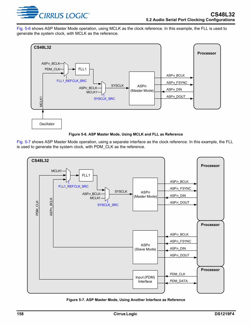
CS48L325.2 Audio Serial Port Clocking Configurations
Fig. 5-6 shows ASP Master Mode operation, using MCLK as the clock reference. In this example, the FLL is used to generate the system clock, with MCLK as the reference.
Figure 5-6. ASP Master Mode, Using MCLK and FLL as Reference
Fig. 5-7 shows ASP Master Mode operation, using a separate interface as the clock reference. In this example, the FLL is used to generate the system clock, with PDM_CLK as the reference.
Figure 5-7. ASP Master Mode, Using Another Interface as Reference
Oscillator
Processor
ASPn_BCLK
ASPn_FSYNC
ASPn_DIN
ASPn_DOUT
FLL1_REFCLK_SRC
FLL1
ASPn(Master Mode)
ASPn_BCLKMCLK1
SYSCLK
SYSCLK_SRC
MC
LK1
PDM_CLK
ASPn_BCLK
CS48L32A
SP
n_B
CLK
Processor
ASPn_BCLK
ASPn_FSYNC
ASPn_DIN
ASPn_DOUT
FLL1_REFCLK_SRC
FLL1
ASPn_BCLK
ASPn_FSYNC
ASPn_DIN
ASPn_DOUT
PDM_CLK
PDM_DATA
PD
M_C
LK
Processor
Processor
ASPn(Master Mode)
ASPn(Slave Mode)
Input (PDM) Interface
ASPn_BCLKMCLK1
SYSCLK
SYSCLK_SRC
MCLK1
CS48L32
158 Cirrus Logic DS1219F4

CS48L325.2 Audio Serial Port Clocking Configurations
Fig. 5-8 shows ASP Slave Mode operation, using BCLK as the clock reference. In this example, the FLL is used to generate the system clock, with BCLK as the reference.
Figure 5-8. ASP Slave Mode, Using BCLK and FLL as Reference
Fig. 5-9 shows ASP Slave Mode operation, using MCLK as the clock reference. For correct operation, the MCLK input must be fully synchronized to the audio serial port.
Figure 5-9. ASP Slave Mode, Using MCLK as Reference
Processor
ASPn_BCLK
ASPn_FSYNC
ASPn_DIN
ASPn_DOUT
FLL1_REFCLK_SRC
FLL1
ASPn(Slave Mode)
PDM_CLKASPn_BCLK
ASPn_BCLKMCLK1
SYSCLK
SYSCLK_SRC
MCLK1
CS48L32
Processor
ASPn_BCLK
ASPn_FSYNC
ASPn_DIN
ASPn_DOUT Synchronous Clock Generator
ASPn(Slave Mode)
SYSCLK
SYSCLK_SRC
MC
LK1
ASPn_BCLKFLL1
CS48L32
DS1219F4 Cirrus Logic 159

CS48L325.2 Audio Serial Port Clocking Configurations
Fig. 5-10 shows ASP Slave Mode operation, using MCLK as the clock reference. For correct operation, the MCLK input must be fully synchronized to the audio serial port. In this example, the FLL is used to generate the system clock, with MCLK as the reference.
Figure 5-10. ASP Slave Mode, Using MCLK and FLL as Reference
Fig. 5-11 shows ASP Slave Mode operation, using a separate interface as the clock reference. In this example, the FLL is used to generate the system clock, with PDM_CLK as the reference. For correct operation, the PDM_CLK input must be fully synchronized to the other audio serial ports.
Figure 5-11. ASP Slave Mode, Using Another Interface as Reference
ASPn_BCLK
ASPn_FSYNC
ASPn_DIN
ASPn_DOUT
Processor
Synchronous Clock Generator
ASPn(Slave Mode)
SYSCLK
SYSCLK_SRC
ASPn_BCLKMCLK1
MC
LK1
PDM_CLK
FLL1_REFCLK_SRC
ASPn_BCLKFLL1
CS48L32
ASPn_BCLK
ASPn_FSYNC
ASPn_DIN
ASPn_DOUT
FLL1_REFCLK_SRC
Processor
Synchronous Clock Generator
AS
Pn_
BC
LK
ASPn_BCLK
ASPn_FSYNC
ASPn_DIN
ASPn_DOUT
PDM_CLK
PDM_DATA
PD
M_C
LK
Processor
Processor
ASPn(Slave Mode)
ASPn(Slave Mode)
Input (PDM) Interface
SYSCLK
SYSCLK_SRC
ASPn_BCLKMCLK1
MCLK1FLL1
CS48L32
160 Cirrus Logic DS1219F4

CS48L325.3 PCB Layout Considerations
5.3 PCB Layout Considerations
PCB layout should be carefully considered, to ensure optimum performance of the CS48L32. Poor PCB layout degrades the performance and is a contributory factor in EMI, ground bounce, and resistive voltage losses. All external components should be placed close to the CS48L32, with current loop areas kept as small as possible. The following specific considerations should be noted:
• Placement of the charge pump capacitors is a high priority requirement—these capacitors (particularly the fly-back capacitor) must be placed as close as possible to the CS48L32.
• Decoupling capacitors should be placed as close as possible to the CS48L32. The connection between GND_A, the VDD_A decoupling capacitor, and the main system ground should be made at a single point as close as possible to the GND_A ball of the CS48L32.
• The VREF_FILT capacitor should be placed as close as possible to the CS48L32. The ground connection to the VREF_FILT capacitor should be as close as possible to the GND_A ball of the CS48L32.
• If multiple power supply rails are connected to a single supply source, it is recommended to provide separate PCB tracks connecting each rail to the supply. This configuration is also known as star connection.
• If power supply rails are routed between different layers of the PCB, it is recommended to use several track vias, in order to minimize resistive voltage losses.
• Differential input signal tracks should be routed as a pair, ensuring similar length/width dimensions on each track. Input signal paths should be kept away from high frequency digital signals.
• Differential output signal tracks should be routed as a pair, ensuring similar length/width dimensions on each track. The tracks should provide a low resistance path from the device output pin to the load (< 1% of the minimum load).
6 Register Map
The CS48L32 control registers are listed in Table 6-1. Note that only the register addresses described here should be accessed; writing to other addresses may result in undefined behavior. Register bits that are not documented should not be changed from the default values.
Table 6-1. Register Map Definition
Register Name 31 15
30 14
29 13
28 12
27 11
26 10
25 9
24 8
23 7
22 6
21 5
20 4
19 3
18 2
17 1
16 0 Default
R0(0x0)
DEVID 0 0 0 0 0 0 0 0 DEVID [23:16] 0x00048A32DEVID [15:0]
R4(0x4)
REVID 0 0 0 0 0 0 0 0 0 0 0 0 0 0 0 0 0x000000A00 0 0 0 0 0 0 0 AREVID [3:0] MTLREVID [3:0]
R32(0x20)
SFT_RESET SFT_RESET [7:0] 0 0 0 0 0 0 0 0 0x000000000 0 0 0 0 0 0 0 0 0 0 0 0 0 0 0
R52(0x34)
USER_KEY_CTRL 0 0 0 0 0 0 0 0 0 0 0 0 0 0 0 0 0x000000000 0 0 0 0 0 0 0 USER_KEY_CTRL[7:0]
R144(0x90)
CTRL_IF_DPHA 0 0 0 0 0 0 0 0 0 0 0 0 0 0 0 0 0x000000000 0 0 0 0 0 0 0 0 0 0 0 0 0 0 SPI1_
DPHA
R3072 (0xC00)
GPIO_STATUS1 0 0 0 0 0 0 0 0 0 0 0 0 0 0 0 0 0x00000000GP16_STSGP15_STSGP14_STSGP13_STSGP12_STSGP11_STSGP10_STS GP9_STS GP8_STS GP7_STS GP6_STS GP5_STS GP4_STS GP3_STS GP2_STS GP1_STS
R3080 (0xC08)
GPIO1_CTRL1 GP1_DIR GP1_PU GP1_PD 0 0 0 0 GP1_DRV_STR
0 0 0 0 GP1_DBTIME [3:0] 0xE1000001
GP1_LVL GP1_OP_CFG
GP1_DB GP1_POL 0 GP1_FN [10:0]
R3084 (0xC0C)
GPIO2_CTRL1 GP2_DIR GP2_PU GP2_PD 0 0 0 0 GP2_DRV_STR
0 0 0 0 GP2_DBTIME [3:0] 0xE1000001
GP2_LVL GP2_OP_CFG
GP2_DB GP2_POL 0 GP2_FN [10:0]
R3088 (0xC10)
GPIO3_CTRL1 GP3_DIR GP3_PU GP3_PD 0 0 0 0 GP3_DRV_STR
0 0 0 0 GP3_DBTIME [3:0] 0xE1000001
GP3_LVL GP3_OP_CFG
GP3_DB GP3_POL 0 GP3_FN [10:0]
R3092 (0xC14)
GPIO4_CTRL1 GP4_DIR GP4_PU GP4_PD 0 0 0 0 GP4_DRV_STR
0 0 0 0 GP4_DBTIME [3:0] 0xE1000001
GP4_LVL GP4_OP_CFG
GP4_DB GP4_POL 0 GP4_FN [10:0]
R3096 (0xC18)
GPIO5_CTRL1 GP5_DIR GP5_PU GP5_PD 0 0 0 0 GP5_DRV_STR
0 0 0 0 GP5_DBTIME [3:0] 0xE1000001
GP5_LVL GP5_OP_CFG
GP5_DB GP5_POL 0 GP5_FN [10:0]
DS1219F4 Cirrus Logic 161

CS48L326 Register Map
R3100 (0xC1C)
GPIO6_CTRL1 GP6_DIR GP6_PU GP6_PD 0 0 0 0 GP6_DRV_STR
0 0 0 0 GP6_DBTIME [3:0] 0xE1000001
GP6_LVL GP6_OP_CFG
GP6_DB GP6_POL 0 GP6_FN [10:0]
R3104 (0xC20)
GPIO7_CTRL1 GP7_DIR GP7_PU GP7_PD 0 0 0 0 GP7_DRV_STR
0 0 0 0 GP7_DBTIME [3:0] 0xE1000001
GP7_LVL GP7_OP_CFG
GP7_DB GP7_POL 0 GP7_FN [10:0]
R3108 (0xC24)
GPIO8_CTRL1 GP8_DIR GP8_PU GP8_PD 0 0 0 0 GP8_DRV_STR
0 0 0 0 GP8_DBTIME [3:0] 0xE1000001
GP8_LVL GP8_OP_CFG
GP8_DB GP8_POL 0 GP8_FN [10:0]
R3112 (0xC28)
GPIO9_CTRL1 GP9_DIR GP9_PU GP9_PD 0 0 0 0 GP9_DRV_STR
0 0 0 0 GP9_DBTIME [3:0] 0xE1000001
GP9_LVL GP9_OP_CFG
GP9_DB GP9_POL 0 GP9_FN [10:0]
R3116 (0xC2C)
GPIO10_CTRL1 GP10_DIR GP10_PU GP10_PD 0 0 0 0 GP10_DRV_STR
0 0 0 0 GP10_DBTIME [3:0] 0xE1000001
GP10_LVL GP10_OP_CFG
GP10_DB GP10_POL
0 GP10_FN [10:0]
R3120 (0xC30)
GPIO11_CTRL1 GP11_DIR GP11_PU GP11_PD 0 0 0 0 GP11_DRV_STR
0 0 0 0 GP11_DBTIME [3:0] 0xE1000001
GP11_LVL GP11_OP_CFG
GP11_DB GP11_POL 0 GP11_FN [10:0]
R3124 (0xC34)
GPIO12_CTRL1 GP12_DIR GP12_PU GP12_PD 0 0 0 0 GP12_DRV_STR
0 0 0 0 GP12_DBTIME [3:0] 0xE1000001
GP12_LVL GP12_OP_CFG
GP12_DB GP12_POL
0 GP12_FN [10:0]
R3128 (0xC38)
GPIO13_CTRL1 GP13_DIR GP13_PU GP13_PD 0 0 0 0 GP13_DRV_STR
0 0 0 0 GP13_DBTIME [3:0] 0xE1000001
GP13_LVL GP13_OP_CFG
GP13_DB GP13_POL
0 GP13_FN [10:0]
R3132 (0xC3C)
GPIO14_CTRL1 GP14_DIR GP14_PU GP14_PD 0 0 0 0 GP14_DRV_STR
0 0 0 0 GP14_DBTIME [3:0] 0xE1000001
GP14_LVL GP14_OP_CFG
GP14_DB GP14_POL
0 GP14_FN [10:0]
R3136 (0xC40)
GPIO15_CTRL1 GP15_DIR GP15_PU GP15_PD 0 0 0 0 GP15_DRV_STR
0 0 0 0 GP15_DBTIME [3:0] 0xE1000001
GP15_LVL GP15_OP_CFG
GP15_DB GP15_POL
0 GP15_FN [10:0]
R3140 (0xC44)
GPIO16_CTRL1 GP16_DIR GP16_PU GP16_PD 0 0 0 0 GP16_DRV_STR
0 0 0 0 GP16_DBTIME [3:0] 0xE1000001
GP16_LVL GP16_OP_CFG
GP16_DB GP16_POL
0 GP16_FN [10:0]
R4100 (0x1004)
SPI1_CFG_1 0 0 0 0 0 0 0 0 0 0 0 0 0 0 0 0 0x000003000 0 0 0 0 0 1 SPI1_
MISO_DRV_STR
SPI1_MISO_PD
0 0 0 0 0 0 0
R4128 (0x1020)
OUTPUT_SYS_CLK 0 0 0 0 0 0 0 0 0 0 0 0 0 0 0 0 0x00000000OPCLK_
EN0 0 0 0 0 0 0 OPCLK_DIV [4:0] OPCLK_SEL [2:0]
R4144 (0x1030)
CLKGEN_PAD_CTRL 0 0 0 0 0 0 0 0 0 0 0 0 0 0 0 0 0x000000000 0 0 0 0 0 0 0 MCLK1_
PD0 0 0 0 0 0 0
R4148 (0x1034)
PDM_PAD_CTRL 0 0 0 0 0 0 0 0 0 0 0 0 0 0 0 0 0x000000000 0 0 0 0 0 0 0 0 0 IN2_
PDMDATA_PD
IN1_PDMDATA
_PD
0 0 0 0
R4156 (0x103C)
MISC_TST_CTRL1 0 0 0 0 0 0 0 0 0 0 0 0 0 0 0 DSP_JTAG_MODE
(K)
0x0000016D
0 0 0 0 0 0 0 1 0 1 1 0 1 1 0 1
R4164 (0x1044)
AUXPDM_CTRL 0 0 0 0 0 0 0 0 0 0 0 0 0 AUXPDM2_CLK_PD
0 AUXPDM1_CLK_PD
0x0000000F
0 0 0 0 0 0 0 0 0 0 0 0 AUXPDM2_CLK_
DRV_STR
AUXPDM2_DOUT_
DRV_STR
AUXPDM1_CLK_
DRV_STR
AUXPDM1_DOUT_
DRV_STR
R4188 (0x105C)
AUXPDM_CTRL2 0 0 0 0 0 0 0 0 0 0 0 0 0 0 0 0 0x000000000 0 0 0 0 0 0 0 AUXPDM2_DOUT_SRC [3:0] AUXPDM1_DOUT_SRC [3:0]
R5120 (0x1400)
CLOCK32K 0 0 0 0 0 0 0 0 0 0 0 0 0 0 0 0 0x000000020 0 0 0 0 0 0 0 0 CLK_32K_
EN0 0 0 0 CLK_32K_SRC [1:0]
R5124 (0x1404)
SYSTEM_CLOCK1 0 0 0 0 0 0 0 0 0 0 0 0 0 0 0 0 0x00000404SYSCLK_
FRAC0 0 0 0 SYSCLK_FREQ [2:0] 0 SYSCLK_
EN0 SYSCLK_SRC [4:0]
R5128 (0x1408)
SYSTEM_CLOCK2 SYSCLK_FREQ_FINE_STS [15:0] 0x000000000 0 0 0 0 SYSCLK_FREQ_STS [2:0] 0 0 0 SYSCLK_SRC_STS [4:0]
R5152 (0x1420)
SAMPLE_RATE1 0 0 0 0 0 0 0 0 0 0 0 0 0 0 0 0 0x000000030 0 0 0 0 0 0 0 0 0 0 SAMPLE_RATE_1 [4:0]
R5156 (0x1424)
SAMPLE_RATE2 0 0 0 0 0 0 0 0 0 0 0 0 0 0 0 0 0x000000030 0 0 0 0 0 0 0 0 0 0 SAMPLE_RATE_2 [4:0]
R5160 (0x1428)
SAMPLE_RATE3 0 0 0 0 0 0 0 0 0 0 0 0 0 0 0 0 0x000000030 0 0 0 0 0 0 0 0 0 0 SAMPLE_RATE_3 [4:0]
Table 6-1. Register Map Definition (Cont.)
Register Name 31 15
30 14
29 13
28 12
27 11
26 10
25 9
24 8
23 7
22 6
21 5
20 4
19 3
18 2
17 1
16 0 Default
162 Cirrus Logic DS1219F4

CS48L326 Register Map
R5164 (0x142C)
SAMPLE_RATE4 0 0 0 0 0 0 0 0 0 0 0 0 0 0 0 0 0x000000030 0 0 0 0 0 0 0 0 0 0 SAMPLE_RATE_4 [4:0]
R5184 (0x1440)
SAMPLE_RATE_STATUS1
0 0 0 0 0 0 0 0 0 0 0 0 0 0 0 0 0x000000000 0 0 0 0 0 0 0 0 0 0 SAMPLE_RATE_1_STS [4:0]
R5188 (0x1444)
SAMPLE_RATE_STATUS2
0 0 0 0 0 0 0 0 0 0 0 0 0 0 0 0 0x000000000 0 0 0 0 0 0 0 0 0 0 SAMPLE_RATE_2_STS [4:0]
R5192 (0x1448)
SAMPLE_RATE_STATUS3
0 0 0 0 0 0 0 0 0 0 0 0 0 0 0 0 0x000000000 0 0 0 0 0 0 0 0 0 0 SAMPLE_RATE_3_STS [4:0]
R5196 (0x144C)
SAMPLE_RATE_STATUS4
0 0 0 0 0 0 0 0 0 0 0 0 0 0 0 0 0x000000000 0 0 0 0 0 0 0 0 0 0 SAMPLE_RATE_4_STS [4:0]
R7168 (0x1C00)
FLL1_CONTROL1 0 0 0 0 0 0 0 0 0 0 0 0 0 0 0 0 0x000000020 0 0 0 0 0 0 0 0 0 0 0 0 FLL1_
CTRL_UPD
FLL1_HOLD
FLL1_EN
R7172 (0x1C04)
FLL1_CONTROL2 FLL1_LOCKDET_THR [3:0] FLL1_LOCKDET
0 0 0 0 FLL1_PHASEDE
T
FLL1_REFDET
0 0 0 FLL1_REFCLK_DIV [1:0]
0x88203004
FLL1_REFCLK_SRC [3:0] 0 0 FLL1_N [9:0]
R7176 (0x1C08)
FLL1_CONTROL3 FLL1_LAMBDA [15:0] 0x00000000FLL1_THETA [15:0]
R7180 (0x1C0C)
FLL1_CONTROL4 FLL1_PD_GAIN_FINE [3:0] FLL1_PD_GAIN_COARSE [3:0] FLL1_FD_GAIN_FINE [3:0] FLL1_FD_GAIN_COARSE [3:0] 0x21F050010 1 FLL1_HP [1:0] 0 0 FLL1_FB_DIV [9:0]
R7328 (0x1CA0)
FLL1_GPIO_CLOCK 0 0 0 0 0 0 0 0 0 0 0 0 0 0 0 0 0x00000C040 0 0 0 FLL1_GPCLK_SRC
[1:0]0 0 FLL1_GPCLK_DIV [6:0] FLL1_
GPCLK_EN
R7220(0x1C34)
FLL1_DIGITAL_TEST2 0 0 0 0 0 0 0 0 0 0 0 0 0 0 0 0 0x000033E80 0 1 1 0 FLL1_FB_
DIV_SDM_ORD2_EN
1 1 1 1 1 0 1 0 0 0
R8192 (0x2000)
CHARGE_PUMP1 0 0 0 0 0 0 0 0 0 0 0 0 0 0 0 0 0x000000060 0 0 0 0 0 0 0 0 0 0 0 0 CP2_
DISCHCP2_
BYPASSCP2_EN
R9224 (0x2408)
LDO2_CTRL1 0 0 0 0 0 0 0 0 0 0 0 0 0 0 0 0 0x000003E40 0 0 0 0 LDO2_VSEL [5:0] 0 0 LDO2_
DISCH0 0
R9232 (0x2410)
MICBIAS_CTRL1 0 0 0 0 0 0 0 0 0 0 0 0 0 0 0 0 0x000000E6MICB1_
EXT_CAP0 0 0 0 0 0 MICB1_LVL [3:0] 0 MICB1_
RATEMICB1_DISCH
MICB1_BYPASS
MICB1_EN
R9240 (0x2418)
MICBIAS_CTRL5 0 0 0 0 0 0 0 0 0 0 0 0 0 0 0 0 0x000002220 0 0 0 0 0 MICB1C_
DISCHMICB1C_
EN0 0 MICB1B_
DISCHMICB1B_
EN0 0 MICB1A_
DISCHMICB1A_
EN
R10000 (0x2710)
IRQ1_CTRL_AOD 0 0 0 0 0 0 0 0 0 0 0 0 0 0 0 0 0x000046000 1 0 0 IRQ1_
MASKIRQ_POL IRQ_OP_
CFG0 0 0 0 0 0 0 0 0
R10008 (0x2718)
AOD_PAD_CTRL 0 0 0 0 0 0 0 0 0 0 0 0 0 0 0 0 0x000040020 1 0 0 0 0 0 0 0 0 0 0 0 0 RESET_
PURESET_
PD
R16384 (0x4000)
INPUT_CONTROL 0 0 0 0 0 0 0 0 0 0 0 0 0 0 0 0 0x000000000 0 0 0 0 0 0 0 0 0 0 0 IN2L_EN IN2R_EN IN1L_EN IN1R_EN
R16388 (0x4004)
INPUT_STATUS 0 0 0 0 0 0 0 0 0 0 0 0 0 0 0 0 0x000000000 0 0 0 0 0 0 0 0 0 0 0 IN2L_STS IN2R_STS IN1L_STS IN1R_STS
R16392 (0x4008)
INPUT_RATE_CONTROL
0 0 0 0 0 0 0 0 0 0 0 0 0 0 0 0 0x00000400IN_RATE [4:0] IN_RATE_
MODE0 0 0 0 0 0 0 0 0 0
R16396 (0x400C)
INPUT_CONTROL2 0 0 0 0 0 0 0 0 0 0 0 0 0 0 0 0 0x000000000 0 0 0 0 0 0 0 0 0 0 0 PDM_FLLCLK_SRC [3:0]
R16404 (0x4014)
INPUT_CONTROL3 0 0 IN_VU 0 0 0 0 0 0 0 0 0 0 0 0 0 0x000000000 0 0 0 0 0 0 0 0 0 0 0 0 0 0 0
R16416 (0x4020)
INPUT1_CONTROL1 0 0 0 0 0 0 0 0 0 0 0 0 0 IN1_OSR [2:0] 0x000500200 0 0 0 0 0 IN1_PDM_SUP [1:0] 0 0 1 0 0 0 0 IN1_
MODE
R16420 (0x4024)
IN1L_CONTROL1 0 0 IN1L_SRC [1:0] 0 0 0 0 0 0 0 0 0 0 0 0 0x00000000IN1L_RATE [4:0] 0 0 0 0 0 0 0 0 IN1L_HPF IN1L_SIG_
DET_ENIN1L_LP_
MODE
R16424 (0x4028)
IN1L_CONTROL2 0 0 0 IN1L_MUTE
0 0 0 0 IN1L_VOL [7:0] 0x10800080
0 0 0 0 0 0 0 0 IN1L_PGA_VOL [6:0] 0
R16452 (0x4044)
IN1R_CONTROL1 0 0 IN1R_SRC [1:0] 0 0 0 0 0 0 0 0 0 0 0 0 0x00000000IN1R_RATE [4:0] 0 0 0 0 0 0 0 0 IN1R_HPF IN1R_
SIG_DET_EN
IN1R_LP_MODE
R16456 (0x4048)
IN1R_CONTROL2 0 0 0 IN1R_MUTE
0 0 0 0 IN1R_VOL [7:0] 0x10800080
0 0 0 0 0 0 0 0 IN1R_PGA_VOL [6:0] 0
R16480 (0x4060)
INPUT2_CONTROL1 0 0 0 0 0 0 0 0 0 0 0 0 0 IN2_OSR [2:0] 0x000500200 0 0 0 0 0 IN2_PDM_SUP [1:0] 0 0 1 0 0 0 0 0
R16484 (0x4064)
IN2L_CONTROL1 0 0 0 0 0 0 0 0 0 0 0 0 0 0 0 0 0x00000000IN2L_RATE [4:0] 0 0 0 0 0 0 0 0 IN2L_HPF IN2L_SIG_
DET_EN0
Table 6-1. Register Map Definition (Cont.)
Register Name 31 15
30 14
29 13
28 12
27 11
26 10
25 9
24 8
23 7
22 6
21 5
20 4
19 3
18 2
17 1
16 0 Default
DS1219F4 Cirrus Logic 163

CS48L326 Register Map
R16488 (0x4068)
IN2L_CONTROL2 0 0 0 IN2L_MUTE
0 0 0 0 IN2L_VOL [7:0] 0x10800000
0 0 0 0 0 0 0 0 0 0 0 0 0 0 0 0
R16516 (0x4084)
IN2R_CONTROL1 0 0 0 0 0 0 0 0 0 0 0 0 0 0 0 0 0x00000000IN2R_RATE [4:0] 0 0 0 0 0 0 0 0 IN2R_HPF IN2R_
SIG_DET_EN
0
R16520 (0x4088)
IN2R_CONTROL2 0 0 0 IN2R_MUTE
0 0 0 0 IN2R_VOL [7:0] 0x10800000
0 0 0 0 0 0 0 0 0 0 0 0 0 0 0 0
R16960 (0x4240)
IN_SIG_DET_CONTROL
0 0 0 0 0 0 0 0 0 0 0 0 0 0 0 0 0x000000010 0 0 0 0 0 0 IN_SIG_DET_THR [4:0] IN_SIG_DET_HOLD [3:0]
R16964 (0x4244)
INPUT_HPF_CONTROL 0 0 0 0 0 0 0 0 0 0 0 0 0 0 0 0 0x000000020 0 0 0 0 0 0 0 0 0 0 0 0 IN_HPF_CUT [2:0]
R16968 (0x4248)
INPUT_VOL_CONTROL 0 0 0 0 0 0 0 0 0 0 0 0 0 0 0 0 0x000000220 0 0 0 0 0 0 0 0 IN_VD_RAMP [2:0] 0 IN_VI_RAMP [2:0]
R17152 (0x4300)
AUXPDM_CONTROL1 0 0 0 0 0 0 0 0 0 0 0 0 0 0 0 0 0x000000000 0 0 0 0 0 0 0 0 0 0 0 0 0 AUXPDM2
_ENAUXPDM1
_EN
R17156 (0x4304)
AUXPDM_CONTROL2 0 0 0 0 0 0 0 0 0 0 0 0 0 0 0 0 0x000000000 0 0 0 0 0 0 0 0 0 0 0 0 0 AUXPDM2
_MUTEAUXPDM1
_MUTE
R17160 (0x4308)
AUXPDM1_CONTROL1 0 0 0 0 0 0 0 0 0 0 0 0 0 0 AUXPDM1_FREQ [1:0]
0x00010008
0 0 0 0 AUXPDM1_SRC [3:0] 0 0 0 AUXPDM1_TXEDGE
AUXPDM1_MSTR
0 0 0
R17168 (0x4310)
AUXPDM2_CONTROL1 0 0 0 0 0 0 0 0 0 0 0 0 0 0 AUXPDM2_FREQ [1:0]
0x00010008
0 0 0 0 AUXPDM2_SRC [3:0] 0 0 0 AUXPDM2_TXEDGE
AUXPDM2_MSTR
0 0 0
R24576 (0x6000)
ASP1_ENABLES1 0 0 0 0 0 0 0 0 ASP1_RX8_EN
ASP1_RX7_EN
ASP1_RX6_EN
ASP1_RX5_EN
ASP1_RX4_EN
ASP1_RX3_EN
ASP1_RX2_EN
ASP1_RX1_EN
0x00000000
0 0 0 0 0 0 0 0 ASP1_TX8_EN
ASP1_TX7_EN
ASP1_TX6_EN
ASP1_TX5_EN
ASP1_TX4_EN
ASP1_TX3_EN
ASP1_TX2_EN
ASP1_TX1_EN
R24580 (0x6004)
ASP1_CONTROL1 0 0 0 0 0 0 0 0 0 0 0 0 0 0 0 0 0x000000280 0 0 ASP1_RATE [4:0] 0 0 ASP1_BCLK_FREQ [5:0]
R24584 (0x6008)
ASP1_CONTROL2 ASP1_RX_WIDTH [7:0] ASP1_TX_WIDTH [7:0] 0x181802000 0 0 0 0 ASP1_FMT [2:0] 0 ASP1_
BCLK_INVASP1_BCLK_FRC
ASP1_BCLK_MSTR
0 ASP1_FSYNC_
INV
ASP1_FSYNC_
FRC
ASP1_FSYNC_MSTR
R24588 (0x600C)
ASP1_CONTROL3 0 0 0 0 0 0 0 0 0 0 0 0 0 0 0 0 0x000000020 0 0 0 0 0 0 0 0 0 0 0 0 0 ASP1_DOUT_HIZ_
CTRL [1:0]
R24592 (0x6010)
ASP1_FRAME_CONTROL1
0 0 ASP1_TX4_SLOT [5:0] 0 0 ASP1_TX3_SLOT [5:0] 0x030201000 0 ASP1_TX2_SLOT [5:0] 0 0 ASP1_TX1_SLOT [5:0]
R24596 (0x6014)
ASP1_FRAME_CONTROL2
0 0 ASP1_TX8_SLOT [5:0] 0 0 ASP1_TX7_SLOT [5:0] 0x070605040 0 ASP1_TX6_SLOT [5:0] 0 0 ASP1_TX5_SLOT [5:0]
R24608 (0x6020)
ASP1_FRAME_CONTROL5
0 0 ASP1_RX4_SLOT [5:0] 0 0 ASP1_RX3_SLOT [5:0] 0x030201000 0 ASP1_RX2_SLOT [5:0] 0 0 ASP1_RX1_SLOT [5:0]
R24612 (0x6024)
ASP1_FRAME_CONTROL6
0 0 ASP1_RX8_SLOT [5:0] 0 0 ASP1_RX7_SLOT [5:0] 0x070605040 0 ASP1_RX6_SLOT [5:0] 0 0 ASP1_RX5_SLOT [5:0]
R24624 (0x6030)
ASP1_DATA_CONTROL1
0 0 0 0 0 0 0 0 0 0 0 0 0 0 0 0 0x000000200 0 0 0 0 0 0 0 0 0 ASP1_TX_WL [5:0]
R24640 (0x6040)
ASP1_DATA_CONTROL5
0 0 0 0 0 0 0 0 0 0 0 0 0 0 0 0 0x000000200 0 0 0 0 0 0 0 0 0 ASP1_RX_WL [5:0]
R24704 (0x6080)
ASP2_ENABLES1 0 0 0 0 0 0 0 0 0 0 0 0 ASP2_RX4_EN
ASP2_RX3_EN
ASP2_RX2_EN
ASP2_RX1_EN
0x00000000
0 0 0 0 0 0 0 0 0 0 0 0 ASP2_TX4_EN
ASP2_TX3_EN
ASP2_TX2_EN
ASP2_TX1_EN
R24708 (0x6084)
ASP2_CONTROL1 0 0 0 0 0 0 0 0 0 0 0 0 0 0 0 0 0x000000280 0 0 ASP2_RATE [4:0] 0 0 ASP2_BCLK_FREQ [5:0]
R24712 (0x6088)
ASP2_CONTROL2 ASP2_RX_WIDTH [7:0] ASP2_TX_WIDTH [7:0] 0x181802000 0 0 0 0 ASP2_FMT [2:0] 0 ASP2_
BCLK_INVASP2_BCLK_FRC
ASP2_BCLK_MSTR
0 ASP2_FSYNC_
INV
ASP2_FSYNC_
FRC
ASP2_FSYNC_MSTR
R24716 (0x608C)
ASP2_CONTROL3 0 0 0 0 0 0 0 0 0 0 0 0 0 0 0 0 0x000000020 0 0 0 0 0 0 0 0 0 0 0 0 0 ASP2_DOUT_HIZ_
CTRL [1:0]
R24720 (0x6090)
ASP2_FRAME_CONTROL1
0 0 ASP2_TX4_SLOT [5:0] 0 0 ASP2_TX3_SLOT [5:0] 0x030201000 0 ASP2_TX2_SLOT [5:0] 0 0 ASP2_TX1_SLOT [5:0]
R24736 (0x60A0)
ASP2_FRAME_CONTROL5
0 0 ASP2_RX4_SLOT [5:0] 0 0 ASP2_RX3_SLOT [5:0] 0x030201000 0 ASP2_RX2_SLOT [5:0] 0 0 ASP2_RX1_SLOT [5:0]
R24752 (0x60B0)
ASP2_DATA_CONTROL1
0 0 0 0 0 0 0 0 0 0 0 0 0 0 0 0 0x000000200 0 0 0 0 0 0 0 0 0 ASP2_TX_WL [5:0]
R24768 (0x60C0)
ASP2_DATA_CONTROL5
0 0 0 0 0 0 0 0 0 0 0 0 0 0 0 0 0x000000200 0 0 0 0 0 0 0 0 0 ASP2_RX_WL [5:0]
R32896 (0x8080)
PWM1_INPUT1 0 0 0 0 0 0 0 0 PWM1MIX_VOL1 [6:0] 0 0x00800000PWM1_SRC1_
STS
0 0 0 0 0 0 PWM1_SRC1 [8:0]
Table 6-1. Register Map Definition (Cont.)
Register Name 31 15
30 14
29 13
28 12
27 11
26 10
25 9
24 8
23 7
22 6
21 5
20 4
19 3
18 2
17 1
16 0 Default
164 Cirrus Logic DS1219F4

CS48L326 Register Map
R32900 (0x8084)
PWM1_INPUT2 0 0 0 0 0 0 0 0 PWM1MIX_VOL2 [6:0] 0 0x00800000PWM1_SRC2_
STS
0 0 0 0 0 0 PWM1_SRC2 [8:0]
R32904 (0x8088)
PWM1_INPUT3 0 0 0 0 0 0 0 0 PWM1MIX_VOL3 [6:0] 0 0x00800000PWM1_SRC3_
STS
0 0 0 0 0 0 PWM1_SRC3 [8:0]
R32908 (0x808C)
PWM1_INPUT4 0 0 0 0 0 0 0 0 PWM1MIX_VOL4 [6:0] 0 0x00800000PWM1_SRC4_
STS
0 0 0 0 0 0 PWM1_SRC4 [8:0]
R32912 (0x8090)
PWM2_INPUT1 0 0 0 0 0 0 0 0 PWM2MIX_VOL1 [6:0] 0 0x00800000PWM2_SRC1_
STS
0 0 0 0 0 0 PWM2_SRC1 [8:0]
R32916 (0x8094)
PWM2_INPUT2 0 0 0 0 0 0 0 0 PWM2MIX_VOL2 [6:0] 0 0x00800000PWM2_SRC2_
STS
0 0 0 0 0 0 PWM2_SRC2 [8:0]
R32920 (0x8098)
PWM2_INPUT3 0 0 0 0 0 0 0 0 PWM2MIX_VOL3 [6:0] 0 0x00800000PWM2_SRC3_
STS
0 0 0 0 0 0 PWM2_SRC3 [8:0]
R32924 (0x809C)
PWM2_INPUT4 0 0 0 0 0 0 0 0 PWM2MIX_VOL4 [6:0] 0 0x00800000PWM2_SRC4_
STS
0 0 0 0 0 0 PWM2_SRC4 [8:0]
R33280 (0x8200)
ASP1TX1_INPUT1 0 0 0 0 0 0 0 0 ASP1TX1MIX_VOL1 [6:0] 0 0x00800000ASP1TX1_
SRC1_STS
0 0 0 0 0 0 ASP1TX1_SRC1 [8:0]
R33284 (0x8204)
ASP1TX1_INPUT2 0 0 0 0 0 0 0 0 ASP1TX1MIX_VOL2 [6:0] 0 0x00800000ASP1TX1_
SRC2_STS
0 0 0 0 0 0 ASP1TX1_SRC2 [8:0]
R33288 (0x8208)
ASP1TX1_INPUT3 0 0 0 0 0 0 0 0 ASP1TX1MIX_VOL3 [6:0] 0 0x00800000ASP1TX1_
SRC3_STS
0 0 0 0 0 0 ASP1TX1_SRC3 [8:0]
R33292 (0x820C)
ASP1TX1_INPUT4 0 0 0 0 0 0 0 0 ASP1TX1MIX_VOL4 [6:0] 0 0x00800000ASP1TX1_
SRC4_STS
0 0 0 0 0 0 ASP1TX1_SRC4 [8:0]
R33296 (0x8210)
ASP1TX2_INPUT1 0 0 0 0 0 0 0 0 ASP1TX2MIX_VOL1 [6:0] 0 0x00800000ASP1TX2_
SRC1_STS
0 0 0 0 0 0 ASP1TX2_SRC1 [8:0]
R33300 (0x8214)
ASP1TX2_INPUT2 0 0 0 0 0 0 0 0 ASP1TX2MIX_VOL2 [6:0] 0 0x00800000ASP1TX2_
SRC2_STS
0 0 0 0 0 0 ASP1TX2_SRC2 [8:0]
R33304 (0x8218)
ASP1TX2_INPUT3 0 0 0 0 0 0 0 0 ASP1TX2MIX_VOL3 [6:0] 0 0x00800000ASP1TX2_
SRC3_STS
0 0 0 0 0 0 ASP1TX2_SRC3 [8:0]
R33308 (0x821C)
ASP1TX2_INPUT4 0 0 0 0 0 0 0 0 ASP1TX2MIX_VOL4 [6:0] 0 0x00800000ASP1TX2_
SRC4_STS
0 0 0 0 0 0 ASP1TX2_SRC4 [8:0]
R33312 (0x8220)
ASP1TX3_INPUT1 0 0 0 0 0 0 0 0 ASP1TX3MIX_VOL1 [6:0] 0 0x00800000ASP1TX3_
SRC1_STS
0 0 0 0 0 0 ASP1TX3_SRC1 [8:0]
R33316 (0x8224)
ASP1TX3_INPUT2 0 0 0 0 0 0 0 0 ASP1TX3MIX_VOL2 [6:0] 0 0x00800000ASP1TX3_
SRC2_STS
0 0 0 0 0 0 ASP1TX3_SRC2 [8:0]
R33320 (0x8228)
ASP1TX3_INPUT3 0 0 0 0 0 0 0 0 ASP1TX3MIX_VOL3 [6:0] 0 0x00800000ASP1TX3_
SRC3_STS
0 0 0 0 0 0 ASP1TX3_SRC3 [8:0]
R33324 (0x822C)
ASP1TX3_INPUT4 0 0 0 0 0 0 0 0 ASP1TX3MIX_VOL4 [6:0] 0 0x00800000ASP1TX3_
SRC4_STS
0 0 0 0 0 0 ASP1TX3_SRC4 [8:0]
R33328 (0x8230)
ASP1TX4_INPUT1 0 0 0 0 0 0 0 0 ASP1TX4MIX_VOL1 [6:0] 0 0x00800000ASP1TX4_
SRC1_STS
0 0 0 0 0 0 ASP1TX4_SRC1 [8:0]
R33332 (0x8234)
ASP1TX4_INPUT2 0 0 0 0 0 0 0 0 ASP1TX4MIX_VOL2 [6:0] 0 0x00800000ASP1TX4_
SRC2_STS
0 0 0 0 0 0 ASP1TX4_SRC2 [8:0]
Table 6-1. Register Map Definition (Cont.)
Register Name 31 15
30 14
29 13
28 12
27 11
26 10
25 9
24 8
23 7
22 6
21 5
20 4
19 3
18 2
17 1
16 0 Default
DS1219F4 Cirrus Logic 165

CS48L326 Register Map
R33336 (0x8238)
ASP1TX4_INPUT3 0 0 0 0 0 0 0 0 ASP1TX4MIX_VOL3 [6:0] 0 0x00800000ASP1TX4_
SRC3_STS
0 0 0 0 0 0 ASP1TX4_SRC3 [8:0]
R33340 (0x823C)
ASP1TX4_INPUT4 0 0 0 0 0 0 0 0 ASP1TX4MIX_VOL4 [6:0] 0 0x00800000ASP1TX4_
SRC4_STS
0 0 0 0 0 0 ASP1TX4_SRC4 [8:0]
R33344 (0x8240)
ASP1TX5_INPUT1 0 0 0 0 0 0 0 0 ASP1TX5MIX_VOL1 [6:0] 0 0x00800000ASP1TX5_
SRC1_STS
0 0 0 0 0 0 ASP1TX5_SRC1 [8:0]
R33348 (0x8244)
ASP1TX5_INPUT2 0 0 0 0 0 0 0 0 ASP1TX5MIX_VOL2 [6:0] 0 0x00800000ASP1TX5_
SRC2_STS
0 0 0 0 0 0 ASP1TX5_SRC2 [8:0]
R33352 (0x8248)
ASP1TX5_INPUT3 0 0 0 0 0 0 0 0 ASP1TX5MIX_VOL3 [6:0] 0 0x00800000ASP1TX5_
SRC3_STS
0 0 0 0 0 0 ASP1TX5_SRC3 [8:0]
R33356 (0x824C)
ASP1TX5_INPUT4 0 0 0 0 0 0 0 0 ASP1TX5MIX_VOL4 [6:0] 0 0x00800000ASP1TX5_
SRC4_STS
0 0 0 0 0 0 ASP1TX5_SRC4 [8:0]
R33360 (0x8250)
ASP1TX6_INPUT1 0 0 0 0 0 0 0 0 ASP1TX6MIX_VOL1 [6:0] 0 0x00800000ASP1TX6_
SRC1_STS
0 0 0 0 0 0 ASP1TX6_SRC1 [8:0]
R33364 (0x8254)
ASP1TX6_INPUT2 0 0 0 0 0 0 0 0 ASP1TX6MIX_VOL2 [6:0] 0 0x00800000ASP1TX6_
SRC2_STS
0 0 0 0 0 0 ASP1TX6_SRC2 [8:0]
R33368 (0x8258)
ASP1TX6_INPUT3 0 0 0 0 0 0 0 0 ASP1TX6MIX_VOL3 [6:0] 0 0x00800000ASP1TX6_
SRC3_STS
0 0 0 0 0 0 ASP1TX6_SRC3 [8:0]
R33372 (0x825C)
ASP1TX6_INPUT4 0 0 0 0 0 0 0 0 ASP1TX6MIX_VOL4 [6:0] 0 0x00800000ASP1TX6_
SRC4_STS
0 0 0 0 0 0 ASP1TX6_SRC4 [8:0]
R33376 (0x8260)
ASP1TX7_INPUT1 0 0 0 0 0 0 0 0 ASP1TX7MIX_VOL1 [6:0] 0 0x00800000ASP1TX7_
SRC1_STS
0 0 0 0 0 0 ASP1TX7_SRC1 [8:0]
R33380 (0x8264)
ASP1TX7_INPUT2 0 0 0 0 0 0 0 0 ASP1TX7MIX_VOL2 [6:0] 0 0x00800000ASP1TX7_
SRC2_STS
0 0 0 0 0 0 ASP1TX7_SRC2 [8:0]
R33384 (0x8268)
ASP1TX7_INPUT3 0 0 0 0 0 0 0 0 ASP1TX7MIX_VOL3 [6:0] 0 0x00800000ASP1TX7_
SRC3_STS
0 0 0 0 0 0 ASP1TX7_SRC3 [8:0]
R33388 (0x826C)
ASP1TX7_INPUT4 0 0 0 0 0 0 0 0 ASP1TX7MIX_VOL4 [6:0] 0 0x00800000ASP1TX7_
SRC4_STS
0 0 0 0 0 0 ASP1TX7_SRC4 [8:0]
R33392 (0x8270)
ASP1TX8_INPUT1 0 0 0 0 0 0 0 0 ASP1TX8MIX_VOL1 [6:0] 0 0x00800000ASP1TX8_
SRC1_STS
0 0 0 0 0 0 ASP1TX8_SRC1 [8:0]
R33396 (0x8274)
ASP1TX8_INPUT2 0 0 0 0 0 0 0 0 ASP1TX8MIX_VOL2 [6:0] 0 0x00800000ASP1TX8_
SRC2_STS
0 0 0 0 0 0 ASP1TX8_SRC2 [8:0]
R33400 (0x8278)
ASP1TX8_INPUT3 0 0 0 0 0 0 0 0 ASP1TX8MIX_VOL3 [6:0] 0 0x00800000ASP1TX8_
SRC3_STS
0 0 0 0 0 0 ASP1TX8_SRC3 [8:0]
R33404 (0x827C)
ASP1TX8_INPUT4 0 0 0 0 0 0 0 0 ASP1TX8MIX_VOL4 [6:0] 0 0x00800000ASP1TX8_
SRC4_STS
0 0 0 0 0 0 ASP1TX8_SRC4 [8:0]
R33536 (0x8300)
ASP2TX1_INPUT1 0 0 0 0 0 0 0 0 ASP2TX1MIX_VOL1 [6:0] 0 0x00800000ASP2TX1_
SRC1_STS
0 0 0 0 0 0 ASP2TX1_SRC1 [8:0]
R33540 (0x8304)
ASP2TX1_INPUT2 0 0 0 0 0 0 0 0 ASP2TX1MIX_VOL2 [6:0] 0 0x00800000ASP2TX1_
SRC2_STS
0 0 0 0 0 0 ASP2TX1_SRC2 [8:0]
R33544 (0x8308)
ASP2TX1_INPUT3 0 0 0 0 0 0 0 0 ASP2TX1MIX_VOL3 [6:0] 0 0x00800000ASP2TX1_
SRC3_STS
0 0 0 0 0 0 ASP2TX1_SRC3 [8:0]
Table 6-1. Register Map Definition (Cont.)
Register Name 31 15
30 14
29 13
28 12
27 11
26 10
25 9
24 8
23 7
22 6
21 5
20 4
19 3
18 2
17 1
16 0 Default
166 Cirrus Logic DS1219F4

CS48L326 Register Map
R33548 (0x830C)
ASP2TX1_INPUT4 0 0 0 0 0 0 0 0 ASP2TX1MIX_VOL4 [6:0] 0 0x00800000ASP2TX1_
SRC4_STS
0 0 0 0 0 0 ASP2TX1_SRC4 [8:0]
R33552 (0x8310)
ASP2TX2_INPUT1 0 0 0 0 0 0 0 0 ASP2TX2MIX_VOL1 [6:0] 0 0x00800000ASP2TX2_
SRC1_STS
0 0 0 0 0 0 ASP2TX2_SRC1 [8:0]
R33556 (0x8314)
ASP2TX2_INPUT2 0 0 0 0 0 0 0 0 ASP2TX2MIX_VOL2 [6:0] 0 0x00800000ASP2TX2_
SRC2_STS
0 0 0 0 0 0 ASP2TX2_SRC2 [8:0]
R33560 (0x8318)
ASP2TX2_INPUT3 0 0 0 0 0 0 0 0 ASP2TX2MIX_VOL3 [6:0] 0 0x00800000ASP2TX2_
SRC3_STS
0 0 0 0 0 0 ASP2TX2_SRC3 [8:0]
R33564 (0x831C)
ASP2TX2_INPUT4 0 0 0 0 0 0 0 0 ASP2TX2MIX_VOL4 [6:0] 0 0x00800000ASP2TX2_
SRC4_STS
0 0 0 0 0 0 ASP2TX2_SRC4 [8:0]
R33568 (0x8320)
ASP2TX3_INPUT1 0 0 0 0 0 0 0 0 ASP2TX3MIX_VOL1 [6:0] 0 0x00800000ASP2TX3_
SRC1_STS
0 0 0 0 0 0 ASP2TX3_SRC1 [8:0]
R33572 (0x8324)
ASP2TX3_INPUT2 0 0 0 0 0 0 0 0 ASP2TX3MIX_VOL2 [6:0] 0 0x00800000ASP2TX3_
SRC2_STS
0 0 0 0 0 0 ASP2TX3_SRC2 [8:0]
R33576 (0x8328)
ASP2TX3_INPUT3 0 0 0 0 0 0 0 0 ASP2TX3MIX_VOL3 [6:0] 0 0x00800000ASP2TX3_
SRC3_STS
0 0 0 0 0 0 ASP2TX3_SRC3 [8:0]
R33580 (0x832C)
ASP2TX3_INPUT4 0 0 0 0 0 0 0 0 ASP2TX3MIX_VOL4 [6:0] 0 0x00800000ASP2TX3_
SRC4_STS
0 0 0 0 0 0 ASP2TX3_SRC4 [8:0]
R33584 (0x8330)
ASP2TX4_INPUT1 0 0 0 0 0 0 0 0 ASP2TX4MIX_VOL1 [6:0] 0 0x00800000ASP2TX4_
SRC1_STS
0 0 0 0 0 0 ASP2TX4_SRC1 [8:0]
R33588 (0x8334)
ASP2TX4_INPUT2 0 0 0 0 0 0 0 0 ASP2TX4MIX_VOL2 [6:0] 0 0x00800000ASP2TX4_
SRC2_STS
0 0 0 0 0 0 ASP2TX4_SRC2 [8:0]
R33592 (0x8338)
ASP2TX4_INPUT3 0 0 0 0 0 0 0 0 ASP2TX4MIX_VOL3 [6:0] 0 0x00800000ASP2TX4_
SRC3_STS
0 0 0 0 0 0 ASP2TX4_SRC3 [8:0]
R33596 (0x833C)
ASP2TX4_INPUT4 0 0 0 0 0 0 0 0 ASP2TX4MIX_VOL4 [6:0] 0 0x00800000ASP2TX4_
SRC4_STS
0 0 0 0 0 0 ASP2TX4_SRC4 [8:0]
R35200 (0x8980)
ISRC1INT1_INPUT1 0 0 0 0 0 0 0 0 0 0 0 0 0 0 0 0 0x00000000ISRC1INT1_SRC1_
STS
0 0 0 0 0 0 ISRC1INT1_SRC1 [8:0]
R35216 (0x8990)
ISRC1INT2_INPUT1 0 0 0 0 0 0 0 0 0 0 0 0 0 0 0 0 0x00000000ISRC1INT2_SRC1_
STS
0 0 0 0 0 0 ISRC1INT2_SRC1 [8:0]
R35232 (0x89A0)
ISRC1INT3_INPUT1 0 0 0 0 0 0 0 0 0 0 0 0 0 0 0 0 0x00000000ISRC1INT3_SRC1_
STS
0 0 0 0 0 0 ISRC1INT3_SRC1 [8:0]
R35248 (0x89B0)
ISRC1INT4_INPUT1 0 0 0 0 0 0 0 0 0 0 0 0 0 0 0 0 0x00000000ISRC1INT4_SRC1_
STS
0 0 0 0 0 0 ISRC1INT4_SRC1 [8:0]
R35264 (0x89C0)
ISRC1DEC1_INPUT1 0 0 0 0 0 0 0 0 0 0 0 0 0 0 0 0 0x00000000ISRC1DEC1_SRC1_
STS
0 0 0 0 0 0 ISRC1DEC1_SRC1 [8:0]
R35280 (0x89D0)
ISRC1DEC2_INPUT1 0 0 0 0 0 0 0 0 0 0 0 0 0 0 0 0 0x00000000ISRC1DEC2_SRC1_
STS
0 0 0 0 0 0 ISRC1DEC2_SRC1 [8:0]
R35296 (0x89E0)
ISRC1DEC3_INPUT1 0 0 0 0 0 0 0 0 0 0 0 0 0 0 0 0 0x00000000ISRC1DEC3_SRC1_
STS
0 0 0 0 0 0 ISRC1DEC3_SRC1 [8:0]
R35312 (0x89F0)
ISRC1DEC4_INPUT1 0 0 0 0 0 0 0 0 0 0 0 0 0 0 0 0 0x00000000ISRC1DEC4_SRC1_
STS
0 0 0 0 0 0 ISRC1DEC4_SRC1 [8:0]
Table 6-1. Register Map Definition (Cont.)
Register Name 31 15
30 14
29 13
28 12
27 11
26 10
25 9
24 8
23 7
22 6
21 5
20 4
19 3
18 2
17 1
16 0 Default
DS1219F4 Cirrus Logic 167

CS48L326 Register Map
R35328 (0x8A00)
ISRC2INT1_INPUT1 0 0 0 0 0 0 0 0 0 0 0 0 0 0 0 0 0x00000000ISRC2INT1_SRC1_
STS
0 0 0 0 0 0 ISRC2INT1_SRC1 [8:0]
R35344 (0x8A10)
ISRC2INT2_INPUT1 0 0 0 0 0 0 0 0 0 0 0 0 0 0 0 0 0x00000000ISRC2INT2_SRC1_
STS
0 0 0 0 0 0 ISRC2INT2_SRC1 [8:0]
R35392 (0x8A40)
ISRC2DEC1_INPUT1 0 0 0 0 0 0 0 0 0 0 0 0 0 0 0 0 0x00000000ISRC2DEC1_SRC1_
STS
0 0 0 0 0 0 ISRC2DEC1_SRC1 [8:0]
R35408 (0x8A50)
ISRC2DEC2_INPUT1 0 0 0 0 0 0 0 0 0 0 0 0 0 0 0 0 0x00000000ISRC2DEC2_SRC1_
STS
0 0 0 0 0 0 ISRC2DEC2_SRC1 [8:0]
R35456 (0x8A80)
ISRC3INT1_INPUT1 0 0 0 0 0 0 0 0 0 0 0 0 0 0 0 0 0x00000000ISRC3INT1_SRC1_
STS
0 0 0 0 0 0 ISRC3INT1_SRC1 [8:0]
R35472 (0x8A90)
ISRC3INT2_INPUT1 0 0 0 0 0 0 0 0 0 0 0 0 0 0 0 0 0x00000000ISRC3INT2_SRC1_
STS
0 0 0 0 0 0 ISRC3INT2_SRC1 [8:0]
R35520 (0x8AC0)
ISRC3DEC1_INPUT1 0 0 0 0 0 0 0 0 0 0 0 0 0 0 0 0 0x00000000ISRC3DEC1_SRC1_
STS
0 0 0 0 0 0 ISRC3DEC1_SRC1 [8:0]
R35536 (0x8AD0)
ISRC3DEC2_INPUT1 0 0 0 0 0 0 0 0 0 0 0 0 0 0 0 0 0x00000000ISRC3DEC2_SRC1_
STS
0 0 0 0 0 0 ISRC3DEC2_SRC1 [8:0]
R35712 (0x8B80)
EQ1_INPUT1 0 0 0 0 0 0 0 0 EQ1MIX_VOL1 [6:0] 0 0x00800000EQ1_
SRC1_STS
0 0 0 0 0 0 EQ1_SRC1 [8:0]
R35716 (0x8B84)
EQ1_INPUT2 0 0 0 0 0 0 0 0 EQ1MIX_VOL2 [6:0] 0 0x00800000EQ1_
SRC2_STS
0 0 0 0 0 0 EQ1_SRC2 [8:0]
R35720 (0x8B88)
EQ1_INPUT3 0 0 0 0 0 0 0 0 EQ1MIX_VOL3 [6:0] 0 0x00800000EQ1_
SRC3_STS
0 0 0 0 0 0 EQ1_SRC3 [8:0]
R35724 (0x8B8C)
EQ1_INPUT4 0 0 0 0 0 0 0 0 EQ1MIX_VOL4 [6:0] 0 0x00800000EQ1_
SRC4_STS
0 0 0 0 0 0 EQ1_SRC4 [8:0]
R35728 (0x8B90)
EQ2_INPUT1 0 0 0 0 0 0 0 0 EQ2MIX_VOL1 [6:0] 0 0x00800000EQ2_
SRC1_STS
0 0 0 0 0 0 EQ2_SRC1 [8:0]
R35732 (0x8B94)
EQ2_INPUT2 0 0 0 0 0 0 0 0 EQ2MIX_VOL2 [6:0] 0 0x00800000EQ2_
SRC2_STS
0 0 0 0 0 0 EQ2_SRC2 [8:0]
R35736 (0x8B98)
EQ2_INPUT3 0 0 0 0 0 0 0 0 EQ2MIX_VOL3 [6:0] 0 0x00800000EQ2_
SRC3_STS
0 0 0 0 0 0 EQ2_SRC3 [8:0]
R35740 (0x8B9C)
EQ2_INPUT4 0 0 0 0 0 0 0 0 EQ2MIX_VOL4 [6:0] 0 0x00800000EQ2_
SRC4_STS
0 0 0 0 0 0 EQ2_SRC4 [8:0]
R35744 (0x8BA0)
EQ3_INPUT1 0 0 0 0 0 0 0 0 EQ3MIX_VOL1 [6:0] 0 0x00800000EQ3_
SRC1_STS
0 0 0 0 0 0 EQ3_SRC1 [8:0]
R35748 (0x8BA4)
EQ3_INPUT2 0 0 0 0 0 0 0 0 EQ3MIX_VOL2 [6:0] 0 0x00800000EQ3_
SRC2_STS
0 0 0 0 0 0 EQ3_SRC2 [8:0]
R35752 (0x8BA8)
EQ3_INPUT3 0 0 0 0 0 0 0 0 EQ3MIX_VOL3 [6:0] 0 0x00800000EQ3_
SRC3_STS
0 0 0 0 0 0 EQ3_SRC3 [8:0]
R35756 (0x8BAC)
EQ3_INPUT4 0 0 0 0 0 0 0 0 EQ3MIX_VOL4 [6:0] 0 0x00800000EQ3_
SRC4_STS
0 0 0 0 0 0 EQ3_SRC4 [8:0]
R35760 (0x8BB0)
EQ4_INPUT1 0 0 0 0 0 0 0 0 EQ4MIX_VOL1 [6:0] 0 0x00800000EQ4_
SRC1_STS
0 0 0 0 0 0 EQ4_SRC1 [8:0]
Table 6-1. Register Map Definition (Cont.)
Register Name 31 15
30 14
29 13
28 12
27 11
26 10
25 9
24 8
23 7
22 6
21 5
20 4
19 3
18 2
17 1
16 0 Default
168 Cirrus Logic DS1219F4

CS48L326 Register Map
R35764 (0x8BB4)
EQ4_INPUT2 0 0 0 0 0 0 0 0 EQ4MIX_VOL2 [6:0] 0 0x00800000EQ4_
SRC2_STS
0 0 0 0 0 0 EQ4_SRC2 [8:0]
R35768 (0x8BB8)
EQ4_INPUT3 0 0 0 0 0 0 0 0 EQ4MIX_VOL3 [6:0] 0 0x00800000EQ4_
SRC3_STS
0 0 0 0 0 0 EQ4_SRC3 [8:0]
R35772 (0x8BBC)
EQ4_INPUT4 0 0 0 0 0 0 0 0 EQ4MIX_VOL4 [6:0] 0 0x00800000EQ4_
SRC4_STS
0 0 0 0 0 0 EQ4_SRC4 [8:0]
R35840 (0x8C00)
DRC1L_INPUT1 0 0 0 0 0 0 0 0 DRC1LMIX_VOL1 [6:0] 0 0x00800000DRC1L_SRC1_
STS
0 0 0 0 0 0 DRC1L_SRC1 [8:0]
R35844 (0x8C04)
DRC1L_INPUT2 0 0 0 0 0 0 0 0 DRC1LMIX_VOL2 [6:0] 0 0x00800000DRC1L_SRC2_
STS
0 0 0 0 0 0 DRC1L_SRC2 [8:0]
R35848 (0x8C08)
DRC1L_INPUT3 0 0 0 0 0 0 0 0 DRC1LMIX_VOL3 [6:0] 0 0x00800000DRC1L_SRC3_
STS
0 0 0 0 0 0 DRC1L_SRC3 [8:0]
R35852 (0x8C0C)
DRC1L_INPUT4 0 0 0 0 0 0 0 0 DRC1LMIX_VOL4 [6:0] 0 0x00800000DRC1L_SRC4_
STS
0 0 0 0 0 0 DRC1L_SRC4 [8:0]
R35856 (0x8C10)
DRC1R_INPUT1 0 0 0 0 0 0 0 0 DRC1RMIX_VOL1 [6:0] 0 0x00800000DRC1R_SRC1_
STS
0 0 0 0 0 0 DRC1R_SRC1 [8:0]
R35860 (0x8C14)
DRC1R_INPUT2 0 0 0 0 0 0 0 0 DRC1RMIX_VOL2 [6:0] 0 0x00800000DRC1R_SRC2_
STS
0 0 0 0 0 0 DRC1R_SRC2 [8:0]
R35864 (0x8C18)
DRC1R_INPUT3 0 0 0 0 0 0 0 0 DRC1RMIX_VOL3 [6:0] 0 0x00800000DRC1R_SRC3_
STS
0 0 0 0 0 0 DRC1R_SRC3 [8:0]
R35868 (0x8C1C)
DRC1R_INPUT4 0 0 0 0 0 0 0 0 DRC1RMIX_VOL4 [6:0] 0 0x00800000DRC1R_SRC4_
STS
0 0 0 0 0 0 DRC1R_SRC4 [8:0]
R35872 (0x8C20)
DRC2L_INPUT1 0 0 0 0 0 0 0 0 DRC2LMIX_VOL1 [6:0] 0 0x00800000DRC2L_SRC1_
STS
0 0 0 0 0 0 DRC2L_SRC1 [8:0]
R35876 (0x8C24)
DRC2L_INPUT2 0 0 0 0 0 0 0 0 DRC2LMIX_VOL2 [6:0] 0 0x00800000DRC2L_SRC2_
STS
0 0 0 0 0 0 DRC2L_SRC2 [8:0]
R35880 (0x8C28)
DRC2L_INPUT3 0 0 0 0 0 0 0 0 DRC2LMIX_VOL3 [6:0] 0 0x00800000DRC2L_SRC3_
STS
0 0 0 0 0 0 DRC2L_SRC3 [8:0]
R35884 (0x8C2C)
DRC2L_INPUT4 0 0 0 0 0 0 0 0 DRC2LMIX_VOL4 [6:0] 0 0x00800000DRC2L_SRC4_
STS
0 0 0 0 0 0 DRC2L_SRC4 [8:0]
R35888 (0x8C30)
DRC2R_INPUT1 0 0 0 0 0 0 0 0 DRC2RMIX_VOL1 [6:0] 0 0x00800000DRC2R_SRC1_
STS
0 0 0 0 0 0 DRC2R_SRC1 [8:0]
R35892 (0x8C34)
DRC2R_INPUT2 0 0 0 0 0 0 0 0 DRC2RMIX_VOL2 [6:0] 0 0x00800000DRC2R_SRC2_
STS
0 0 0 0 0 0 DRC2R_SRC2 [8:0]
R35896 (0x8C38)
DRC2R_INPUT3 0 0 0 0 0 0 0 0 DRC2RMIX_VOL3 [6:0] 0 0x00800000DRC2R_SRC3_
STS
0 0 0 0 0 0 DRC2R_SRC3 [8:0]
R35900 (0x8C3C)
DRC2R_INPUT4 0 0 0 0 0 0 0 0 DRC2RMIX_VOL4 [6:0] 0 0x00800000DRC2R_SRC4_
STS
0 0 0 0 0 0 DRC2R_SRC4 [8:0]
R35968 (0x8C80)
LHPF1_INPUT1 0 0 0 0 0 0 0 0 LHPF1MIX_VOL1 [6:0] 0 0x00800000LHPF1_SRC1_
STS
0 0 0 0 0 0 LHPF1_SRC1 [8:0]
R35972 (0x8C84)
LHPF1_INPUT2 0 0 0 0 0 0 0 0 LHPF1MIX_VOL2 [6:0] 0 0x00800000LHPF1_SRC2_
STS
0 0 0 0 0 0 LHPF1_SRC2 [8:0]
Table 6-1. Register Map Definition (Cont.)
Register Name 31 15
30 14
29 13
28 12
27 11
26 10
25 9
24 8
23 7
22 6
21 5
20 4
19 3
18 2
17 1
16 0 Default
DS1219F4 Cirrus Logic 169

CS48L326 Register Map
R35976 (0x8C88)
LHPF1_INPUT3 0 0 0 0 0 0 0 0 LHPF1MIX_VOL3 [6:0] 0 0x00800000LHPF1_SRC3_
STS
0 0 0 0 0 0 LHPF1_SRC3 [8:0]
R35980 (0x8C8C)
LHPF1_INPUT4 0 0 0 0 0 0 0 0 LHPF1MIX_VOL4 [6:0] 0 0x00800000LHPF1_SRC4_
STS
0 0 0 0 0 0 LHPF1_SRC4 [8:0]
R35984 (0x8C90)
LHPF2_INPUT1 0 0 0 0 0 0 0 0 LHPF2MIX_VOL1 [6:0] 0 0x00800000LHPF2_SRC1_
STS
0 0 0 0 0 0 LHPF2_SRC1 [8:0]
R35988 (0x8C94)
LHPF2_INPUT2 0 0 0 0 0 0 0 0 LHPF2MIX_VOL2 [6:0] 0 0x00800000LHPF2_SRC2_
STS
0 0 0 0 0 0 LHPF2_SRC2 [8:0]
R35992 (0x8C98)
LHPF2_INPUT3 0 0 0 0 0 0 0 0 LHPF2MIX_VOL3 [6:0] 0 0x00800000LHPF2_SRC3_
STS
0 0 0 0 0 0 LHPF2_SRC3 [8:0]
R35996 (0x8C9C)
LHPF2_INPUT4 0 0 0 0 0 0 0 0 LHPF2MIX_VOL4 [6:0] 0 0x00800000LHPF2_SRC4_
STS
0 0 0 0 0 0 LHPF2_SRC4 [8:0]
R36000 (0x8CA0)
LHPF3_INPUT1 0 0 0 0 0 0 0 0 LHPF3MIX_VOL1 [6:0] 0 0x00800000LHPF3_SRC1_
STS
0 0 0 0 0 0 LHPF3_SRC1 [8:0]
R36004 (0x8CA4)
LHPF3_INPUT2 0 0 0 0 0 0 0 0 LHPF3MIX_VOL2 [6:0] 0 0x00800000LHPF3_SRC2_
STS
0 0 0 0 0 0 LHPF3_SRC2 [8:0]
R36008 (0x8CA8)
LHPF3_INPUT3 0 0 0 0 0 0 0 0 LHPF3MIX_VOL3 [6:0] 0 0x00800000LHPF3_SRC3_
STS
0 0 0 0 0 0 LHPF3_SRC3 [8:0]
R36012 (0x8CAC)
LHPF3_INPUT4 0 0 0 0 0 0 0 0 LHPF3MIX_VOL4 [6:0] 0 0x00800000LHPF3_SRC4_
STS
0 0 0 0 0 0 LHPF3_SRC4 [8:0]
R36016 (0x8CB0)
LHPF4_INPUT1 0 0 0 0 0 0 0 0 LHPF4MIX_VOL1 [6:0] 0 0x00800000LHPF4_SRC1_
STS
0 0 0 0 0 0 LHPF4_SRC1 [8:0]
R36020 (0x8CB4)
LHPF4_INPUT2 0 0 0 0 0 0 0 0 LHPF4MIX_VOL2 [6:0] 0 0x00800000LHPF4_SRC2_
STS
0 0 0 0 0 0 LHPF4_SRC2 [8:0]
R36024 (0x8CB8)
LHPF4_INPUT3 0 0 0 0 0 0 0 0 LHPF4MIX_VOL3 [6:0] 0 0x00800000LHPF4_SRC3_
STS
0 0 0 0 0 0 LHPF4_SRC3 [8:0]
R36028 (0x8CBC)
LHPF4_INPUT4 0 0 0 0 0 0 0 0 LHPF4MIX_VOL4 [6:0] 0 0x00800000LHPF4_SRC4_
STS
0 0 0 0 0 0 LHPF4_SRC4 [8:0]
R36864 (0x9000)
DSP1RX1_INPUT1 0 0 0 0 0 0 0 0 DSP1RX1MIX_VOL1 [6:0] 0 0x00800000DSP1RX1_SRC1_
STS
0 0 0 0 0 0 DSP1RX1_SRC1 [8:0]
R36868 (0x9004)
DSP1RX1_INPUT2 0 0 0 0 0 0 0 0 DSP1RX1MIX_VOL2 [6:0] 0 0x00800000DSP1RX1_SRC2_
STS
0 0 0 0 0 0 DSP1RX1_SRC2 [8:0]
R36872 (0x9008)
DSP1RX1_INPUT3 0 0 0 0 0 0 0 0 DSP1RX1MIX_VOL3 [6:0] 0 0x00800000DSP1RX1_SRC3_
STS
0 0 0 0 0 0 DSP1RX1_SRC3 [8:0]
R36876 (0x900C)
DSP1RX1_INPUT4 0 0 0 0 0 0 0 0 DSP1RX1MIX_VOL4 [6:0] 0 0x00800000DSP1RX1_SRC4_
STS
0 0 0 0 0 0 DSP1RX1_SRC4 [8:0]
R36880 (0x9010)
DSP1RX2_INPUT1 0 0 0 0 0 0 0 0 DSP1RX2MIX_VOL1 [6:0] 0 0x00800000DSP1RX2_SRC1_
STS
0 0 0 0 0 0 DSP1RX2_SRC1 [8:0]
R36884 (0x9014)
DSP1RX2_INPUT2 0 0 0 0 0 0 0 0 DSP1RX2MIX_VOL2 [6:0] 0 0x00800000DSP1RX2_SRC2_
STS
0 0 0 0 0 0 DSP1RX2_SRC2 [8:0]
R36888 (0x9018)
DSP1RX2_INPUT3 0 0 0 0 0 0 0 0 DSP1RX2MIX_VOL3 [6:0] 0 0x00800000DSP1RX2_SRC3_
STS
0 0 0 0 0 0 DSP1RX2_SRC3 [8:0]
Table 6-1. Register Map Definition (Cont.)
Register Name 31 15
30 14
29 13
28 12
27 11
26 10
25 9
24 8
23 7
22 6
21 5
20 4
19 3
18 2
17 1
16 0 Default
170 Cirrus Logic DS1219F4

CS48L326 Register Map
R36892 (0x901C)
DSP1RX2_INPUT4 0 0 0 0 0 0 0 0 DSP1RX2MIX_VOL4 [6:0] 0 0x00800000DSP1RX2_SRC4_
STS
0 0 0 0 0 0 DSP1RX2_SRC4 [8:0]
R36896 (0x9020)
DSP1RX3_INPUT1 0 0 0 0 0 0 0 0 DSP1RX3MIX_VOL1 [6:0] 0 0x00800000DSP1RX3_SRC1_
STS
0 0 0 0 0 0 DSP1RX3_SRC1 [8:0]
R36900 (0x9024)
DSP1RX3_INPUT2 0 0 0 0 0 0 0 0 DSP1RX3MIX_VOL2 [6:0] 0 0x00800000DSP1RX3_SRC2_
STS
0 0 0 0 0 0 DSP1RX3_SRC2 [8:0]
R36904 (0x9028)
DSP1RX3_INPUT3 0 0 0 0 0 0 0 0 DSP1RX3MIX_VOL3 [6:0] 0 0x00800000DSP1RX3_SRC3_
STS
0 0 0 0 0 0 DSP1RX3_SRC3 [8:0]
R36908 (0x902C)
DSP1RX3_INPUT4 0 0 0 0 0 0 0 0 DSP1RX3MIX_VOL4 [6:0] 0 0x00800000DSP1RX3_SRC4_
STS
0 0 0 0 0 0 DSP1RX3_SRC4 [8:0]
R36912 (0x9030)
DSP1RX4_INPUT1 0 0 0 0 0 0 0 0 DSP1RX4MIX_VOL1 [6:0] 0 0x00800000DSP1RX4_SRC1_
STS
0 0 0 0 0 0 DSP1RX4_SRC1 [8:0]
R36916 (0x9034)
DSP1RX4_INPUT2 0 0 0 0 0 0 0 0 DSP1RX4MIX_VOL2 [6:0] 0 0x00800000DSP1RX4_SRC2_
STS
0 0 0 0 0 0 DSP1RX4_SRC2 [8:0]
R36920 (0x9038)
DSP1RX4_INPUT3 0 0 0 0 0 0 0 0 DSP1RX4MIX_VOL3 [6:0] 0 0x00800000DSP1RX4_SRC3_
STS
0 0 0 0 0 0 DSP1RX4_SRC3 [8:0]
R36924 (0x903C)
DSP1RX4_INPUT4 0 0 0 0 0 0 0 0 DSP1RX4MIX_VOL4 [6:0] 0 0x00800000DSP1RX4_SRC4_
STS
0 0 0 0 0 0 DSP1RX4_SRC4 [8:0]
R36928 (0x9040)
DSP1RX5_INPUT1 0 0 0 0 0 0 0 0 DSP1RX5MIX_VOL1 [6:0] 0 0x00800000DSP1RX5_SRC1_
STS
0 0 0 0 0 0 DSP1RX5_SRC1 [8:0]
R36932 (0x9044)
DSP1RX5_INPUT2 0 0 0 0 0 0 0 0 DSP1RX5MIX_VOL2 [6:0] 0 0x00800000DSP1RX5_SRC2_
STS
0 0 0 0 0 0 DSP1RX5_SRC2 [8:0]
R36936 (0x9048)
DSP1RX5_INPUT3 0 0 0 0 0 0 0 0 DSP1RX5MIX_VOL3 [6:0] 0 0x00800000DSP1RX5_SRC3_
STS
0 0 0 0 0 0 DSP1RX5_SRC3 [8:0]
R36940 (0x904C)
DSP1RX5_INPUT4 0 0 0 0 0 0 0 0 DSP1RX5MIX_VOL4 [6:0] 0 0x00800000DSP1RX5_SRC4_
STS
0 0 0 0 0 0 DSP1RX5_SRC4 [8:0]
R36944 (0x9050)
DSP1RX6_INPUT1 0 0 0 0 0 0 0 0 DSP1RX6MIX_VOL1 [6:0] 0 0x00800000DSP1RX6_SRC1_
STS
0 0 0 0 0 0 DSP1RX6_SRC1 [8:0]
R36948 (0x9054)
DSP1RX6_INPUT2 0 0 0 0 0 0 0 0 DSP1RX6MIX_VOL2 [6:0] 0 0x00800000DSP1RX6_SRC2_
STS
0 0 0 0 0 0 DSP1RX6_SRC2 [8:0]
R36952 (0x9058)
DSP1RX6_INPUT3 0 0 0 0 0 0 0 0 DSP1RX6MIX_VOL3 [6:0] 0 0x00800000DSP1RX6_SRC3_
STS
0 0 0 0 0 0 DSP1RX6_SRC3 [8:0]
R36956 (0x905C)
DSP1RX6_INPUT4 0 0 0 0 0 0 0 0 DSP1RX6MIX_VOL4 [6:0] 0 0x00800000DSP1RX6_SRC4_
STS
0 0 0 0 0 0 DSP1RX6_SRC4 [8:0]
R36960 (0x9060)
DSP1RX7_INPUT1 0 0 0 0 0 0 0 0 DSP1RX7MIX_VOL1 [6:0] 0 0x00800000DSP1RX7_SRC1_
STS
0 0 0 0 0 0 DSP1RX7_SRC1 [8:0]
R36964 (0x9064)
DSP1RX7_INPUT2 0 0 0 0 0 0 0 0 DSP1RX7MIX_VOL2 [6:0] 0 0x00800000DSP1RX7_SRC2_
STS
0 0 0 0 0 0 DSP1RX7_SRC2 [8:0]
R36968 (0x9068)
DSP1RX7_INPUT3 0 0 0 0 0 0 0 0 DSP1RX7MIX_VOL3 [6:0] 0 0x00800000DSP1RX7_SRC3_
STS
0 0 0 0 0 0 DSP1RX7_SRC3 [8:0]
R36972 (0x906C)
DSP1RX7_INPUT4 0 0 0 0 0 0 0 0 DSP1RX7MIX_VOL4 [6:0] 0 0x00800000DSP1RX7_SRC4_
STS
0 0 0 0 0 0 DSP1RX7_SRC4 [8:0]
Table 6-1. Register Map Definition (Cont.)
Register Name 31 15
30 14
29 13
28 12
27 11
26 10
25 9
24 8
23 7
22 6
21 5
20 4
19 3
18 2
17 1
16 0 Default
DS1219F4 Cirrus Logic 171

CS48L326 Register Map
R36976 (0x9070)
DSP1RX8_INPUT1 0 0 0 0 0 0 0 0 DSP1RX8MIX_VOL1 [6:0] 0 0x00800000DSP1RX8_SRC1_
STS
0 0 0 0 0 0 DSP1RX8_SRC1 [8:0]
R36980 (0x9074)
DSP1RX8_INPUT2 0 0 0 0 0 0 0 0 DSP1RX8MIX_VOL2 [6:0] 0 0x00800000DSP1RX8_SRC2_
STS
0 0 0 0 0 0 DSP1RX8_SRC2 [8:0]
R36984 (0x9078)
DSP1RX8_INPUT3 0 0 0 0 0 0 0 0 DSP1RX8MIX_VOL3 [6:0] 0 0x00800000DSP1RX8_SRC3_
STS
0 0 0 0 0 0 DSP1RX8_SRC3 [8:0]
R36988 (0x907C)
DSP1RX8_INPUT4 0 0 0 0 0 0 0 0 DSP1RX8MIX_VOL4 [6:0] 0 0x00800000DSP1RX8_SRC4_
STS
0 0 0 0 0 0 DSP1RX8_SRC4 [8:0]
R41984 (0xA400)
ISRC1_CONTROL1 ISRC1_FSL [4:0] 0 0 0 0 0 0 0 0 0 0 0 0x00000000ISRC1_FSH [4:0] 0 0 0 0 0 0 0 0 0 0 0
R41988 (0xA404)
ISRC1_CONTROL2 0 0 0 0 0 0 0 0 0 0 0 0 0 0 0 0 0x000000000 0 0 0 ISRC1_
INT4_ENISRC1_
INT3_ENISRC1_
INT2_ENISRC1_
INT1_EN0 0 0 0 ISRC1_
DEC4_ENISRC1_
DEC3_ENISRC1_
DEC2_ENISRC1_
DEC1_EN
R42256 (0xA510)
ISRC2_CONTROL1 ISRC2_FSL [4:0] 0 0 0 0 0 0 0 0 0 0 0 0x00000000ISRC2_FSH [4:0] 0 0 0 0 0 0 0 0 0 0 0
R42260 (0xA514)
ISRC2_CONTROL2 0 0 0 0 0 0 0 0 0 0 0 0 0 0 0 0 0x000000000 0 0 0 0 0 ISRC2_
INT2_ENISRC2_
INT1_EN0 0 0 0 0 0 ISRC2_
DEC2_ENISRC2_
DEC1_EN
R42528 (0xA620)
ISRC3_CONTROL1 ISRC3_FSL [4:0] 0 0 0 0 0 0 0 0 0 0 0 0x00000000ISRC3_FSH [4:0] 0 0 0 0 0 0 0 0 0 0 0
R42532 (0xA624)
ISRC3_CONTROL2 0 0 0 0 0 0 0 0 0 0 0 0 0 0 0 0 0x000000000 0 0 0 0 0 ISRC3_
INT2_ENISRC3_
INT1_EN0 0 0 0 0 0 ISRC3_
DEC2_ENISRC3_
DEC1_EN
R43008 (0xA800)
FX_SAMPLE_RATE 0 0 0 0 0 0 0 0 0 0 0 0 0 0 0 0 0x00000000FX_RATE [4:0] 0 0 0 0 0 0 0 0 0 0 0
R43012 (0xA804)
FX_STATUS 0 0 0 0 0 0 0 0 0 0 0 0 0 0 0 0 0x000000000 0 0 0 FX_STS [11:0]
R43016 (0xA808)
EQ_CONTROL1 0 0 0 0 0 0 0 0 0 0 0 0 0 0 0 0 0x000000000 0 0 0 0 0 0 0 0 0 0 0 EQ4_EN EQ3_EN EQ2_EN EQ1_EN
R43020 (0xA80C)
EQ_CONTROL2 0 0 0 0 0 0 0 0 0 0 0 0 0 0 0 0 0x000000000 0 0 0 0 0 0 0 0 0 0 0 EQ4_B1_
MODEEQ3_B1_
MODEEQ2_B1_
MODEEQ1_B1_
MODE
R43024 (0xA810)
EQ1_GAIN1 0 0 0 EQ1_B4_GAIN [4:0] 0 0 0 EQ1_B3_GAIN [4:0] 0x0C0C0C0C0 0 0 EQ1_B2_GAIN [4:0] 0 0 0 EQ1_B1_GAIN [4:0]
R43028 (0xA814)
EQ1_GAIN2 0 0 0 0 0 0 0 0 0 0 0 0 0 0 0 0 0x0000000C0 0 0 0 0 0 0 0 0 0 0 EQ1_B5_GAIN [4:0]
R43032 (0xA818)
EQ1_BAND1_COEFF1 EQ1_B1_B [15:0] 0x03FE0FC8EQ1_B1_A [15:0]
R43036 (0xA81C)
EQ1_BAND1_COEFF2 0 0 0 0 0 0 0 0 0 0 0 0 0 0 0 0 0x00000B75EQ1_B1_C [15:0]
R43040 (0xA820)
EQ1_BAND1_PG 0 0 0 0 0 0 0 0 0 0 0 0 0 0 0 0 0x000000E0EQ1_B1_PG [15:0]
R43044 (0xA824)
EQ1_BAND2_COEFF1 EQ1_B2_B [15:0] 0xF1361EC4EQ1_B2_A [15:0]
R43048 (0xA828)
EQ1_BAND2_COEFF2 0 0 0 0 0 0 0 0 0 0 0 0 0 0 0 0 0x00000409EQ1_B2_C [15:0]
R43052 (0xA82C)
EQ1_BAND2_PG 0 0 0 0 0 0 0 0 0 0 0 0 0 0 0 0 0x000004CCEQ1_B2_PG [15:0]
R43056 (0xA830)
EQ1_BAND3_COEFF1 EQ1_B3_B [15:0] 0xF3371C9BEQ1_B3_A [15:0]
R43060 (0xA834)
EQ1_BAND3_COEFF2 0 0 0 0 0 0 0 0 0 0 0 0 0 0 0 0 0x0000040BEQ1_B3_C [15:0]
R43064 (0xA838)
EQ1_BAND3_PG 0 0 0 0 0 0 0 0 0 0 0 0 0 0 0 0 0x00000CBBEQ1_B3_PG [15:0]
R43068 (0xA83C)
EQ1_BAND4_COEFF1 EQ1_B4_B [15:0] 0xF7D916F8EQ1_B4_A [15:0]
R43072 (0xA840)
EQ1_BAND4_COEFF2 0 0 0 0 0 0 0 0 0 0 0 0 0 0 0 0 0x0000040AEQ1_B4_C [15:0]
R43076 (0xA844)
EQ1_BAND4_PG 0 0 0 0 0 0 0 0 0 0 0 0 0 0 0 0 0x00001F14EQ1_B4_PG [15:0]
R43080 (0xA848)
EQ1_BAND5_COEFF1 EQ1_B5_B [15:0] 0x0563058CEQ1_B5_A [15:0]
R43088 (0xA850)
EQ1_BAND5_PG 0 0 0 0 0 0 0 0 0 0 0 0 0 0 0 0 0x00004000EQ1_B5_PG [15:0]
R43092 (0xA854)
EQ2_GAIN1 0 0 0 EQ2_B4_GAIN [4:0] 0 0 0 EQ2_B3_GAIN [4:0] 0x0C0C0C0C0 0 0 EQ2_B2_GAIN [4:0] 0 0 0 EQ2_B1_GAIN [4:0]
R43096 (0xA858)
EQ2_GAIN2 0 0 0 0 0 0 0 0 0 0 0 0 0 0 0 0 0x0000000C0 0 0 0 0 0 0 0 0 0 0 EQ2_B5_GAIN [4:0]
Table 6-1. Register Map Definition (Cont.)
Register Name 31 15
30 14
29 13
28 12
27 11
26 10
25 9
24 8
23 7
22 6
21 5
20 4
19 3
18 2
17 1
16 0 Default
172 Cirrus Logic DS1219F4
CS48L326 Register Map
R43100 (0xA85C)
EQ2_BAND1_COEFF1 EQ2_B1_B [15:0] 0x03FE0FC8EQ2_B1_A [15:0]
R43104 (0xA860)
EQ2_BAND1_COEFF2 0 0 0 0 0 0 0 0 0 0 0 0 0 0 0 0 0x00000B75EQ2_B1_C [15:0]
R43108 (0xA864)
EQ2_BAND1_PG 0 0 0 0 0 0 0 0 0 0 0 0 0 0 0 0 0x000000E0EQ2_B1_PG [15:0]
R43112 (0xA868)
EQ2_BAND2_COEFF1 EQ2_B2_B [15:0] 0xF1361EC4EQ2_B2_A [15:0]
R43116 (0xA86C)
EQ2_BAND2_COEFF2 0 0 0 0 0 0 0 0 0 0 0 0 0 0 0 0 0x00000409EQ2_B2_C [15:0]
R43120 (0xA870)
EQ2_BAND2_PG 0 0 0 0 0 0 0 0 0 0 0 0 0 0 0 0 0x000004CCEQ2_B2_PG [15:0]
R43124 (0xA874)
EQ2_BAND3_COEFF1 EQ2_B3_B [15:0] 0xF3371C9BEQ2_B3_A [15:0]
R43128 (0xA878)
EQ2_BAND3_COEFF2 0 0 0 0 0 0 0 0 0 0 0 0 0 0 0 0 0x0000040BEQ2_B3_C [15:0]
R43132 (0xA87C)
EQ2_BAND3_PG 0 0 0 0 0 0 0 0 0 0 0 0 0 0 0 0 0x00000CBBEQ2_B3_PG [15:0]
R43136 (0xA880)
EQ2_BAND4_COEFF1 EQ2_B4_B [15:0] 0xF7D916F8EQ2_B4_A [15:0]
R43140 (0xA884)
EQ2_BAND4_COEFF2 0 0 0 0 0 0 0 0 0 0 0 0 0 0 0 0 0x0000040AEQ2_B4_C [15:0]
R43144 (0xA888)
EQ2_BAND4_PG 0 0 0 0 0 0 0 0 0 0 0 0 0 0 0 0 0x00001F14EQ2_B4_PG [15:0]
R43148 (0xA88C)
EQ2_BAND5_COEFF1 EQ2_B5_B [15:0] 0x0563058CEQ2_B5_A [15:0]
R43156 (0xA894)
EQ2_BAND5_PG 0 0 0 0 0 0 0 0 0 0 0 0 0 0 0 0 0x00004000EQ2_B5_PG [15:0]
R43160 (0xA898)
EQ3_GAIN1 0 0 0 EQ3_B4_GAIN [4:0] 0 0 0 EQ3_B3_GAIN [4:0] 0x0C0C0C0C0 0 0 EQ3_B2_GAIN [4:0] 0 0 0 EQ3_B1_GAIN [4:0]
R43164 (0xA89C)
EQ3_GAIN2 0 0 0 0 0 0 0 0 0 0 0 0 0 0 0 0 0x0000000C0 0 0 0 0 0 0 0 0 0 0 EQ3_B5_GAIN [4:0]
R43168 (0xA8A0)
EQ3_BAND1_COEFF1 EQ3_B1_B [15:0] 0x03FE0FC8EQ3_B1_A [15:0]
R43172 (0xA8A4)
EQ3_BAND1_COEFF2 0 0 0 0 0 0 0 0 0 0 0 0 0 0 0 0 0x00000B75EQ3_B1_C [15:0]
R43176 (0xA8A8)
EQ3_BAND1_PG 0 0 0 0 0 0 0 0 0 0 0 0 0 0 0 0 0x000000E0EQ3_B1_PG [15:0]
R43180 (0xA8AC)
EQ3_BAND2_COEFF1 EQ3_B2_B [15:0] 0xF1361EC4EQ3_B2_A [15:0]
R43184 (0xA8B0)
EQ3_BAND2_COEFF2 0 0 0 0 0 0 0 0 0 0 0 0 0 0 0 0 0x00000409EQ3_B2_C [15:0]
R43188 (0xA8B4)
EQ3_BAND2_PG 0 0 0 0 0 0 0 0 0 0 0 0 0 0 0 0 0x000004CCEQ3_B2_PG [15:0]
R43192 (0xA8B8)
EQ3_BAND3_COEFF1 EQ3_B3_B [15:0] 0xF3371C9BEQ3_B3_A [15:0]
R43196 (0xA8BC)
EQ3_BAND3_COEFF2 0 0 0 0 0 0 0 0 0 0 0 0 0 0 0 0 0x0000040BEQ3_B3_C [15:0]
R43200 (0xA8C0)
EQ3_BAND3_PG 0 0 0 0 0 0 0 0 0 0 0 0 0 0 0 0 0x00000CBBEQ3_B3_PG [15:0]
R43204 (0xA8C4)
EQ3_BAND4_COEFF1 EQ3_B4_B [15:0] 0xF7D916F8EQ3_B4_A [15:0]
R43208 (0xA8C8)
EQ3_BAND4_COEFF2 0 0 0 0 0 0 0 0 0 0 0 0 0 0 0 0 0x0000040AEQ3_B4_C [15:0]
R43212 (0xA8CC)
EQ3_BAND4_PG 0 0 0 0 0 0 0 0 0 0 0 0 0 0 0 0 0x00001F14EQ3_B4_PG [15:0]
R43216 (0xA8D0)
EQ3_BAND5_COEFF1 EQ3_B5_B [15:0] 0x0563058CEQ3_B5_A [15:0]
R43224 (0xA8D8)
EQ3_BAND5_PG 0 0 0 0 0 0 0 0 0 0 0 0 0 0 0 0 0x00004000EQ3_B5_PG [15:0]
R43228 (0xA8DC)
EQ4_GAIN1 0 0 0 EQ4_B4_GAIN [4:0] 0 0 0 EQ4_B3_GAIN [4:0] 0x0C0C0C0C0 0 0 EQ4_B2_GAIN [4:0] 0 0 0 EQ4_B1_GAIN [4:0]
R43232 (0xA8E0)
EQ4_GAIN2 0 0 0 0 0 0 0 0 0 0 0 0 0 0 0 0 0x0000000C0 0 0 0 0 0 0 0 0 0 0 EQ4_B5_GAIN [4:0]
R43236 (0xA8E4)
EQ4_BAND1_COEFF1 EQ4_B1_B [15:0] 0x03FE0FC8EQ4_B1_A [15:0]
R43240 (0xA8E8)
EQ4_BAND1_COEFF2 0 0 0 0 0 0 0 0 0 0 0 0 0 0 0 0 0x00000B75EQ4_B1_C [15:0]
R43244 (0xA8EC)
EQ4_BAND1_PG 0 0 0 0 0 0 0 0 0 0 0 0 0 0 0 0 0x000000E0EQ4_B1_PG [15:0]
R43248 (0xA8F0)
EQ4_BAND2_COEFF1 EQ4_B2_B [15:0] 0xF1361EC4EQ4_B2_A [15:0]
Table 6-1. Register Map Definition (Cont.)
Register Name 31 15
30 14
29 13
28 12
27 11
26 10
25 9
24 8
23 7
22 6
21 5
20 4
19 3
18 2
17 1
16 0 Default
DS1219F4 Cirrus Logic 173

CS48L326 Register Map
R43252 (0xA8F4)
EQ4_BAND2_COEFF2 0 0 0 0 0 0 0 0 0 0 0 0 0 0 0 0 0x00000409EQ4_B2_C [15:0]
R43256 (0xA8F8)
EQ4_BAND2_PG 0 0 0 0 0 0 0 0 0 0 0 0 0 0 0 0 0x000004CCEQ4_B2_PG [15:0]
R43260 (0xA8FC)
EQ4_BAND3_COEFF1 EQ4_B3_B [15:0] 0xF3371C9BEQ4_B3_A [15:0]
R43264 (0xA900)
EQ4_BAND3_COEFF2 0 0 0 0 0 0 0 0 0 0 0 0 0 0 0 0 0x0000040BEQ4_B3_C [15:0]
R43268 (0xA904)
EQ4_BAND3_PG 0 0 0 0 0 0 0 0 0 0 0 0 0 0 0 0 0x00000CBBEQ4_B3_PG [15:0]
R43272 (0xA908)
EQ4_BAND4_COEFF1 EQ4_B4_B [15:0] 0xF7D916F8EQ4_B4_A [15:0]
R43276 (0xA90C)
EQ4_BAND4_COEFF2 0 0 0 0 0 0 0 0 0 0 0 0 0 0 0 0 0x0000040AEQ4_B4_C [15:0]
R43280 (0xA910)
EQ4_BAND4_PG 0 0 0 0 0 0 0 0 0 0 0 0 0 0 0 0 0x00001F14EQ4_B4_PG [15:0]
R43284 (0xA914)
EQ4_BAND5_COEFF1 EQ4_B5_B [15:0] 0x0563058CEQ4_B5_A [15:0]
R43292 (0xA91C)
EQ4_BAND5_PG 0 0 0 0 0 0 0 0 0 0 0 0 0 0 0 0 0x00004000EQ4_B5_PG [15:0]
R43568 (0xAA30)
LHPF_CONTROL1 0 0 0 0 0 0 0 0 0 0 0 0 0 0 0 0 0x000000000 0 0 0 0 0 0 0 0 0 0 0 LHPF4_ENLHPF3_ENLHPF2_ENLHPF1_EN
R43572 (0xAA34)
LHPF_CONTROL2 0 0 0 0 0 0 0 0 0 0 0 0 0 0 0 0 0x000000000 0 0 0 0 0 0 0 0 0 0 0 LHPF4_
MODELHPF3_MODE
LHPF2_MODE
LHPF1_MODE
R43576 (0xAA38)
LHPF1_COEFF 0 0 0 0 0 0 0 0 0 0 0 0 0 0 0 0 0x00000000LHPF1_COEFF [15:0]
R43580 (0xAA3C)
LHPF2_COEFF 0 0 0 0 0 0 0 0 0 0 0 0 0 0 0 0 0x00000000LHPF2_COEFF [15:0]
R43584 (0xAA40)
LHPF3_COEFF 0 0 0 0 0 0 0 0 0 0 0 0 0 0 0 0 0x00000000LHPF3_COEFF [15:0]
R43588 (0xAA44)
LHPF4_COEFF 0 0 0 0 0 0 0 0 0 0 0 0 0 0 0 0 0x00000000LHPF4_COEFF [15:0]
R43776 (0xAB00)
DRC1_CONTROL1 0 0 0 0 0 0 0 0 0 0 0 0 0 0 0 0 0x000000000 0 0 0 0 0 0 0 0 0 0 0 0 0 DRC1L_
ENDRC1R_
EN
R43780 (0xAB04)
DRC1_CONTROL2 DRC1_ATK [3:0] DRC1_DCY [3:0] 0 0 0 DRC1_MINGAIN [2:0] DRC1_MAXGAIN [1:0] 0x49130018DRC1_SIG_DET_RMS [4:0] DRC1_SIG_DET_PK
[1:0]DRC1_NG_EN
DRC1_SIG_DET_
MODE
DRC1_SIG_DET
DRC1_KNEE2_OP_EN
DRC1_QR DRC1_ANTICLIP
0 0 0
R43784 (0xAB08)
DRC1_CONTROL3 0 0 0 0 0 0 0 0 0 0 0 0 0 0 0 0 0x00000018DRC1_NG_MINGAIN [3:0] DRC1_NG_EXP [1:0] DRC1_QR_THR [1:0] DRC1_QR_DCY [1:0] DRC1_HI_COMP [2:0] DRC1_LO_COMP [2:0]
R43788 (0xAB0C)
DRC1_CONTROL4 0 0 0 DRC1_KNEE2_IP [4:0] 0 0 0 DRC1_KNEE2_OP [4:0] 0x000000000 0 DRC1_KNEE1_IP [5:0] 0 0 0 DRC1_KNEE1_OP [4:0]
R43796 (0xAB14)
DRC2_CONTROL1 0 0 0 0 0 0 0 0 0 0 0 0 0 0 0 0 0x000000000 0 0 0 0 0 0 0 0 0 0 0 0 0 DRC2L_
ENDRC2R_
EN
R43800 (0xAB18)
DRC2_CONTROL2 DRC2_ATK [3:0] DRC2_DCY [3:0] 0 0 0 DRC2_MINGAIN [2:0] DRC2_MAXGAIN [1:0] 0x49130018DRC2_SIG_DET_RMS [4:0] DRC2_SIG_DET_PK
[1:0]DRC2_NG_EN
DRC2_SIG_DET_
MODE
DRC2_SIG_DET
DRC2_KNEE2_OP_EN
DRC2_QR DRC2_ANTICLIP
0 0 0
R43804 (0xAB1C)
DRC2_CONTROL3 0 0 0 0 0 0 0 0 0 0 0 0 0 0 0 0 0x00000018DRC2_NG_MINGAIN [3:0] DRC2_NG_EXP [1:0] DRC2_QR_THR [1:0] DRC2_QR_DCY [1:0] DRC2_HI_COMP [2:0] DRC2_LO_COMP [2:0]
R43808 (0xAB20)
DRC2_CONTROL4 0 0 0 DRC2_KNEE2_IP [4:0] 0 0 0 DRC2_KNEE2_OP [4:0] 0x000000000 0 DRC2_KNEE1_IP [5:0] 0 0 0 DRC2_KNEE1_OP [4:0]
R45056 (0xB000)
TONE_GENERATOR1 0 0 0 0 0 0 0 0 0 0 0 0 0 0 0 0 0x00000000TONE_RATE [4:0] 0 TONE_OFFSET [1:0] 0 0 TONE2_
OVDTONE1_
OVD0 0 TONE2_
ENTONE1_
EN
R45060 (0xB004)
TONE_GENERATOR2 0 0 0 0 0 0 0 0 TONE1_LVL [23:16] 0x00100000TONE1_LVL [15:0]
R45064 (0xB008)
TONE_GENERATOR3 0 0 0 0 0 0 0 0 TONE2_LVL [23:16] 0x00100000TONE2_LVL [15:0]
R46080 (0xB400)
Comfort_Noise_Generator
0 0 0 0 0 0 0 0 0 0 0 0 0 0 0 0 0x00000000NOISE_GEN_RATE [4:0] 0 0 0 0 0 NOISE_
GEN_ENNOISE_GEN_GAIN [4:0]
R47104 (0xB800)
US_CONTROL 0 0 0 0 0 0 0 0 0 0 0 0 0 0 0 0 0x000000000 0 0 0 0 0 US2_DET_
ENUS1_DET_
EN0 0 0 0 0 0 US2_EN US1_EN
R47108 (0xB804)
US1_CONTROL US1_RATE [4:0] 0 0 0 0 0 0 0 0 0 0 0 0x000020200 0 US1_GAIN [1:0] US1_SRC [3:0] 0 US1_FREQ [2:0] 0 0 0 0
R47112 (0xB808)
US1_DET_CONTROL 0 US1_DET_DCY [2:0] US1_DET_HOLD [3:0] US1_DET_NUM [3:0] 0 US1_DET_THR [2:0] 0x000000000 0 0 0 0 0 0 0 0 US1_DET_LPF_CUT
[1:0]US1_DET_
LPF0 0 0 0
R47124 (0xB814)
US2_CONTROL US2_RATE [4:0] 0 0 0 0 0 0 0 0 0 0 0 0x000020200 0 US2_GAIN [1:0] US2_SRC [3:0] 0 US2_FREQ [2:0] 0 0 0 0
Table 6-1. Register Map Definition (Cont.)
Register Name 31 15
30 14
29 13
28 12
27 11
26 10
25 9
24 8
23 7
22 6
21 5
20 4
19 3
18 2
17 1
16 0 Default
174 Cirrus Logic DS1219F4

CS48L326 Register Map
R47128 (0xB818)
US2_DET_CONTROL 0 US2_DET_DCY [2:0] US2_DET_HOLD [3:0] US2_DET_NUM [3:0] 0 US2_DET_THR [2:0] 0x000000000 0 0 0 0 0 0 0 0 US2_DET_LPF_CUT
[1:0]US2_DET_
LPF0 0 0 0
R49152 (0xC000)
PWM_Drive_1 0 0 0 0 0 0 0 0 0 0 0 0 0 0 0 0 0x00000000PWM_RATE [4:0] PWM_CLK_SEL [2:0] 0 0 PWM2_
OVDPWM1_
OVD0 0 PWM2_ENPWM1_EN
R49156 (0xC004)
PWM_Drive_2 0 0 0 0 0 0 0 0 0 0 0 0 0 0 0 0 0x000001000 0 0 0 0 0 PWM1_LVL [9:0]
R49160 (0xC008)
PWM_Drive_3 0 0 0 0 0 0 0 0 0 0 0 0 0 0 0 0 0x000001000 0 0 0 0 0 PWM2_LVL [9:0]
R94220 (0x1700C)
DSP1_XM_SRAM_IBUS_SETUP_0
0 0 0 0 0 0 0 0 0 0 0 0 0 0 0 0 0x000000000 0 0 0 0 0 0 0 0 0 0 0 0 0 DSP1_
XM_SRAM_
IBUS_E_PWD_N
DSP1_XM_
SRAM_IBUS_O_PWD_N
R94224 (0x17010)
DSP1_XM_SRAM_IBUS_SETUP_1
0 0 0 0 0 0 0 0 0 0 0 0 0 0 0 0 0x000000000 0 0 0 0 0 0 0 0 0 0 0 0 0 DSP1_
XM_SRAM_
IBUS_E_EXT_N_1
DSP1_XM_
SRAM_IBUS_O_EXT_N_1
R94228 (0x17014)
DSP1_XM_SRAM_IBUS_SETUP_2
0 0 0 0 0 0 0 0 0 0 0 0 0 0 0 0 0x000000000 0 0 0 0 0 0 0 0 0 0 0 0 0 DSP1_
XM_SRAM_
IBUS_E_EXT_N_2
DSP1_XM_
SRAM_IBUS_O_EXT_N_2
R94232 (0x17018)
DSP1_XM_SRAM_IBUS_SETUP_3
0 0 0 0 0 0 0 0 0 0 0 0 0 0 0 0 0x000000000 0 0 0 0 0 0 0 0 0 0 0 0 0 DSP1_
XM_SRAM_
IBUS_E_EXT_N_3
DSP1_XM_
SRAM_IBUS_O_EXT_N_3
R94236 (0x1701C)
DSP1_XM_SRAM_IBUS_SETUP_4
0 0 0 0 0 0 0 0 0 0 0 0 0 0 0 0 0x000000000 0 0 0 0 0 0 0 0 0 0 0 0 0 DSP1_
XM_SRAM_
IBUS_E_EXT_N_4
DSP1_XM_
SRAM_IBUS_O_EXT_N_4
R94240 (0x17020)
DSP1_XM_SRAM_IBUS_SETUP_5
0 0 0 0 0 0 0 0 0 0 0 0 0 0 0 0 0x000000000 0 0 0 0 0 0 0 0 0 0 0 0 0 DSP1_
XM_SRAM_
IBUS_E_EXT_N_5
DSP1_XM_
SRAM_IBUS_O_EXT_N_5
R94244 (0x17024)
DSP1_XM_SRAM_IBUS_SETUP_6
0 0 0 0 0 0 0 0 0 0 0 0 0 0 0 0 0x000000000 0 0 0 0 0 0 0 0 0 0 0 0 0 DSP1_
XM_SRAM_
IBUS_E_EXT_N_6
DSP1_XM_
SRAM_IBUS_O_EXT_N_6
R94248 (0x17028)
DSP1_XM_SRAM_IBUS_SETUP_7
0 0 0 0 0 0 0 0 0 0 0 0 0 0 0 0 0x000000000 0 0 0 0 0 0 0 0 0 0 0 0 0 DSP1_
XM_SRAM_
IBUS_E_EXT_N_7
DSP1_XM_
SRAM_IBUS_O_EXT_N_7
R94252 (0x1702C)
DSP1_XM_SRAM_IBUS_SETUP_8
0 0 0 0 0 0 0 0 0 0 0 0 0 0 0 0 0x000000000 0 0 0 0 0 0 0 0 0 0 0 0 0 DSP1_
XM_SRAM_
IBUS_E_EXT_N_8
DSP1_XM_
SRAM_IBUS_O_EXT_N_8
R94256 (0x17030)
DSP1_XM_SRAM_IBUS_SETUP_9
0 0 0 0 0 0 0 0 0 0 0 0 0 0 0 0 0x000000000 0 0 0 0 0 0 0 0 0 0 0 0 0 DSP1_
XM_SRAM_
IBUS_E_EXT_N_9
DSP1_XM_
SRAM_IBUS_O_EXT_N_9
R94260 (0x17034)
DSP1_XM_SRAM_IBUS_SETUP_10
0 0 0 0 0 0 0 0 0 0 0 0 0 0 0 0 0x000000000 0 0 0 0 0 0 0 0 0 0 0 0 0 DSP1_
XM_SRAM_
IBUS_E_EXT_N_10
DSP1_XM_
SRAM_IBUS_O_
EXT_N_10
R94264 (0x17038)
DSP1_XM_SRAM_IBUS_SETUP_11
0 0 0 0 0 0 0 0 0 0 0 0 0 0 0 0 0x000000000 0 0 0 0 0 0 0 0 0 0 0 0 0 DSP1_
XM_SRAM_
IBUS_E_EXT_N_11
DSP1_XM_
SRAM_IBUS_O_
EXT_N_11
R94268 (0x1703C)
DSP1_XM_SRAM_IBUS_SETUP_12
0 0 0 0 0 0 0 0 0 0 0 0 0 0 0 0 0x000000000 0 0 0 0 0 0 0 0 0 0 0 0 0 DSP1_
XM_SRAM_
IBUS_E_EXT_N_12
DSP1_XM_
SRAM_IBUS_O_
EXT_N_12
Table 6-1. Register Map Definition (Cont.)
Register Name 31 15
30 14
29 13
28 12
27 11
26 10
25 9
24 8
23 7
22 6
21 5
20 4
19 3
18 2
17 1
16 0 Default
DS1219F4 Cirrus Logic 175

CS48L326 Register Map
R94272 (0x17040)
DSP1_XM_SRAM_IBUS_SETUP_13
0 0 0 0 0 0 0 0 0 0 0 0 0 0 0 0 0x000000000 0 0 0 0 0 0 0 0 0 0 0 0 0 DSP1_
XM_SRAM_
IBUS_E_EXT_N_13
DSP1_XM_
SRAM_IBUS_O_
EXT_N_13
R94276 (0x17044)
DSP1_XM_SRAM_IBUS_SETUP_14
0 0 0 0 0 0 0 0 0 0 0 0 0 0 0 0 0x000000000 0 0 0 0 0 0 0 0 0 0 0 0 0 DSP1_
XM_SRAM_
IBUS_E_EXT_N_14
DSP1_XM_
SRAM_IBUS_O_
EXT_N_14
R94280 (0x17048)
DSP1_XM_SRAM_IBUS_SETUP_15
0 0 0 0 0 0 0 0 0 0 0 0 0 0 0 0 0x000000000 0 0 0 0 0 0 0 0 0 0 0 0 0 DSP1_
XM_SRAM_
IBUS_E_EXT_N_15
DSP1_XM_
SRAM_IBUS_O_
EXT_N_15
R94284 (0x1704C)
DSP1_XM_SRAM_IBUS_SETUP_16
0 0 0 0 0 0 0 0 0 0 0 0 0 0 0 0 0x000000000 0 0 0 0 0 0 0 0 0 0 0 0 0 DSP1_
XM_SRAM_
IBUS_E_EXT_N_16
DSP1_XM_
SRAM_IBUS_O_
EXT_N_16
R94288 (0x17050)
DSP1_XM_SRAM_IBUS_SETUP_17
0 0 0 0 0 0 0 0 0 0 0 0 0 0 0 0 0x000000000 0 0 0 0 0 0 0 0 0 0 0 0 0 DSP1_
XM_SRAM_
IBUS_E_EXT_N_17
DSP1_XM_
SRAM_IBUS_O_
EXT_N_17
R94292 (0x17054)
DSP1_XM_SRAM_IBUS_SETUP_18
0 0 0 0 0 0 0 0 0 0 0 0 0 0 0 0 0x000000000 0 0 0 0 0 0 0 0 0 0 0 0 0 DSP1_
XM_SRAM_
IBUS_E_EXT_N_18
DSP1_XM_
SRAM_IBUS_O_
EXT_N_18
R94296 (0x17058)
DSP1_XM_SRAM_IBUS_SETUP_19
0 0 0 0 0 0 0 0 0 0 0 0 0 0 0 0 0x000000000 0 0 0 0 0 0 0 0 0 0 0 0 0 DSP1_
XM_SRAM_
IBUS_E_EXT_N_19
DSP1_XM_
SRAM_IBUS_O_
EXT_N_19
R94300 (0x1705C)
DSP1_XM_SRAM_IBUS_SETUP_20
0 0 0 0 0 0 0 0 0 0 0 0 0 0 0 0 0x000000000 0 0 0 0 0 0 0 0 0 0 0 0 0 DSP1_
XM_SRAM_
IBUS_E_EXT_N_20
DSP1_XM_
SRAM_IBUS_O_
EXT_N_20
R94304 (0x17060)
DSP1_XM_SRAM_IBUS_SETUP_21
0 0 0 0 0 0 0 0 0 0 0 0 0 0 0 0 0x000000000 0 0 0 0 0 0 0 0 0 0 0 0 0 DSP1_
XM_SRAM_
IBUS_E_EXT_N_21
DSP1_XM_
SRAM_IBUS_O_
EXT_N_21
R94308 (0x17064)
DSP1_XM_SRAM_IBUS_SETUP_22
0 0 0 0 0 0 0 0 0 0 0 0 0 0 0 0 0x000000000 0 0 0 0 0 0 0 0 0 0 0 0 0 DSP1_
XM_SRAM_
IBUS_E_EXT_N_22
DSP1_XM_
SRAM_IBUS_O_
EXT_N_22
R94312 (0x17068)
DSP1_XM_SRAM_IBUS_SETUP_23
0 0 0 0 0 0 0 0 0 0 0 0 0 0 0 0 0x000000000 0 0 0 0 0 0 0 0 0 0 0 0 0 DSP1_
XM_SRAM_
IBUS_E_EXT_N_23
DSP1_XM_
SRAM_IBUS_O_
EXT_N_23
R94316 (0x1706C)
DSP1_XM_SRAM_IBUS_SETUP_24
0 0 0 0 0 0 0 0 0 0 0 0 0 0 0 0 0x000000000 0 0 0 0 0 0 0 0 0 0 0 0 0 DSP1_
XM_SRAM_
IBUS_E_EXT_N_24
DSP1_XM_
SRAM_IBUS_O_
EXT_N_24
R94320 (0x17070)
DSP1_YM_SRAM_IBUS_SETUP_0
0 0 0 0 0 0 0 0 0 0 0 0 0 0 0 0 0x000000000 0 0 0 0 0 0 0 0 0 0 0 0 0 DSP1_
YM_SRAM_
IBUS_E_PWD_N
DSP1_YM_
SRAM_IBUS_O_PWD_N
R94324 (0x17074)
DSP1_YM_SRAM_IBUS_SETUP_1
0 0 0 0 0 0 0 0 0 0 0 0 0 0 0 0 0x000000000 0 0 0 0 0 0 0 0 0 0 0 0 0 DSP1_
YM_SRAM_
IBUS_E_EXT_N_1
DSP1_YM_
SRAM_IBUS_O_EXT_N_1
R94328 (0x17078)
DSP1_YM_SRAM_IBUS_SETUP_2
0 0 0 0 0 0 0 0 0 0 0 0 0 0 0 0 0x000000000 0 0 0 0 0 0 0 0 0 0 0 0 0 DSP1_
YM_SRAM_
IBUS_E_EXT_N_2
DSP1_YM_
SRAM_IBUS_O_EXT_N_2
Table 6-1. Register Map Definition (Cont.)
Register Name 31 15
30 14
29 13
28 12
27 11
26 10
25 9
24 8
23 7
22 6
21 5
20 4
19 3
18 2
17 1
16 0 Default
176 Cirrus Logic DS1219F4

CS48L326 Register Map
R94332 (0x1707C)
DSP1_YM_SRAM_IBUS_SETUP_3
0 0 0 0 0 0 0 0 0 0 0 0 0 0 0 0 0x000000000 0 0 0 0 0 0 0 0 0 0 0 0 0 DSP1_
YM_SRAM_
IBUS_E_EXT_N_3
DSP1_YM_
SRAM_IBUS_O_EXT_N_3
R94336 (0x17080)
DSP1_YM_SRAM_IBUS_SETUP_4
0 0 0 0 0 0 0 0 0 0 0 0 0 0 0 0 0x000000000 0 0 0 0 0 0 0 0 0 0 0 0 0 DSP1_
YM_SRAM_
IBUS_E_EXT_N_4
DSP1_YM_
SRAM_IBUS_O_EXT_N_4
R94340 (0x17084)
DSP1_YM_SRAM_IBUS_SETUP_5
0 0 0 0 0 0 0 0 0 0 0 0 0 0 0 0 0x000000000 0 0 0 0 0 0 0 0 0 0 0 0 0 DSP1_
YM_SRAM_
IBUS_E_EXT_N_5
DSP1_YM_
SRAM_IBUS_O_EXT_N_5
R94344 (0x17088)
DSP1_YM_SRAM_IBUS_SETUP_6
0 0 0 0 0 0 0 0 0 0 0 0 0 0 0 0 0x000000000 0 0 0 0 0 0 0 0 0 0 0 0 0 DSP1_
YM_SRAM_
IBUS_E_EXT_N_6
DSP1_YM_
SRAM_IBUS_O_EXT_N_6
R94348 (0x1708C)
DSP1_YM_SRAM_IBUS_SETUP_7
0 0 0 0 0 0 0 0 0 0 0 0 0 0 0 0 0x000000000 0 0 0 0 0 0 0 0 0 0 0 0 0 DSP1_
YM_SRAM_
IBUS_E_EXT_N_7
DSP1_YM_
SRAM_IBUS_O_EXT_N_7
R94352 (0x17090)
DSP1_YM_SRAM_IBUS_SETUP_8
0 0 0 0 0 0 0 0 0 0 0 0 0 0 0 0 0x000000000 0 0 0 0 0 0 0 0 0 0 0 0 0 DSP1_
YM_SRAM_
IBUS_E_EXT_N_8
DSP1_YM_
SRAM_IBUS_O_EXT_N_8
R94356 (0x17094)
DSP1_PM_SRAM_IBUS_SETUP_0
0 0 0 0 0 0 0 0 0 0 0 0 0 0 0 0 0x000000000 0 0 0 0 0 0 0 0 0 0 0 0 0 DSP1_
PM_SRAM_
IBUS_E_PWD_N
DSP1_PM_
SRAM_IBUS_O_PWD_N
R94360 (0x17098)
DSP1_PM_SRAM_IBUS_SETUP_1
0 0 0 0 0 0 0 0 0 0 0 0 0 0 0 0 0x000000000 0 0 0 0 0 0 0 0 0 0 0 0 0 DSP1_
PM_SRAM_
IBUS_E_EXT_N_1
DSP1_PM_
SRAM_IBUS_O_EXT_N_1
R94364 (0x1709C)
DSP1_PM_SRAM_IBUS_SETUP_2
0 0 0 0 0 0 0 0 0 0 0 0 0 0 0 0 0x000000000 0 0 0 0 0 0 0 0 0 0 0 0 0 DSP1_
PM_SRAM_
IBUS_E_EXT_N_2
DSP1_PM_
SRAM_IBUS_O_EXT_N_2
R94368 (0x170A0)
DSP1_PM_SRAM_IBUS_SETUP_3
0 0 0 0 0 0 0 0 0 0 0 0 0 0 0 0 0x000000000 0 0 0 0 0 0 0 0 0 0 0 0 0 DSP1_
PM_SRAM_
IBUS_E_EXT_N_3
DSP1_PM_
SRAM_IBUS_O_EXT_N_3
R94372 (0x170A4)
DSP1_PM_SRAM_IBUS_SETUP_4
0 0 0 0 0 0 0 0 0 0 0 0 0 0 0 0 0x000000000 0 0 0 0 0 0 0 0 0 0 0 0 0 DSP1_
PM_SRAM_
IBUS_E_EXT_N_4
DSP1_PM_
SRAM_IBUS_O_EXT_N_4
R94376 (0x170A8)
DSP1_PM_SRAM_IBUS_SETUP_5
0 0 0 0 0 0 0 0 0 0 0 0 0 0 0 0 0x000000000 0 0 0 0 0 0 0 0 0 0 0 0 0 DSP1_
PM_SRAM_
IBUS_E_EXT_N_5
DSP1_PM_
SRAM_IBUS_O_EXT_N_5
R94380 (0x170AC)
DSP1_PM_SRAM_IBUS_SETUP_6
0 0 0 0 0 0 0 0 0 0 0 0 0 0 0 0 0x000000000 0 0 0 0 0 0 0 0 0 0 0 0 0 DSP1_
PM_SRAM_
IBUS_E_EXT_N_6
DSP1_PM_
SRAM_IBUS_O_EXT_N_6
R94384 (0x170B0)
DSP1_PM_SRAM_IBUS_SETUP_7
0 0 0 0 0 0 0 0 0 0 0 0 0 0 0 0 0x000000000 0 0 0 0 0 0 0 0 0 0 0 0 0 DSP1_
PM_SRAM_
IBUS_E_EXT_N_7
DSP1_PM_
SRAM_IBUS_O_EXT_N_7
R98308 (0x18004)
IRQ1_STATUS 0 0 0 0 0 0 0 0 0 0 0 0 0 0 0 0 0x000000000 0 0 0 0 0 0 0 0 0 0 0 0 0 0 IRQ1_STS
R98320 (0x18010)
IRQ1_EINT_1 0 0 0 0 0 0 0 0 0 0 0 0 0 0 0 0 0x000000000 0 0 0 0 SYSCLK_
ERR_EINT1
0 SYSCLK_FAIL_EINT1
0 0 0 0 0 0 0 0
Table 6-1. Register Map Definition (Cont.)
Register Name 31 15
30 14
29 13
28 12
27 11
26 10
25 9
24 8
23 7
22 6
21 5
20 4
19 3
18 2
17 1
16 0 Default
DS1219F4 Cirrus Logic 177

CS48L326 Register Map
R98324 (0x18014)
IRQ1_EINT_2 0 0 0 0 0 0 0 0 0 0 0 0 0 0 0 0 0x000000000 0 0 0 0 0 0 0 0 0 0 0 BOOT_
DONE_EINT1
0 0 0
R98336 (0x18020)
IRQ1_EINT_5 0 0 0 0 0 0 US2_SIG_DET_FALL_EINT1
US2_SIG_DET_RISE_EINT1
US1_SIG_DET_FALL_EINT1
US1_SIG_DET_RISE_EINT1
INPUTS_SIG_DET_
FALL_EINT1
INPUTS_SIG_DET_
RISE_EINT1
DRC2_SIG_DET_
FALL_EINT1
DRC2_SIG_DET_
RISE_EINT1
DRC1_SIG_DET_
FALL_EINT1
DRC1_SIG_DET_
RISE_EINT1
0x00000000
0 0 0 0 0 0 0 0 0 0 0 0 0 0 0 0
R98340 (0x18024)
IRQ1_EINT_6 0 0 0 0 0 0 0 0 0 0 0 0 0 0 0 0 0x000000000 0 0 0 0 0 0 FLL1_
REF_LOST_EINT1
0 0 0 0 0 0 FLL1_LOCK_FALL_EINT1
FLL1_LOCK_RISE_EINT1
R98344 (0x18028)
IRQ1_EINT_7 0 0 0 0 0 0 0 0 0 0 DSP1_MPU_ERR_EINT1
DSP1_WDT_
EXPIRE_EINT1
DSP1_IHB_ERR_
EINT1
DSP1_AHB_SYS_ERR_EINT1
DSP1_AHB_
PACK_ERR_EINT1
DSP1_NMI_ERR_
EINT1
0x00000000
0 0 0 0 0 0 0 0 0 0 0 0 0 0 0 0
R98352 (0x18030)
IRQ1_EINT_9 MCU_HWERR_
IRQ_OUT_EINT1
0 0 0 0 0 0 0 0 0 0 0 0 0 0 0 0x00000000
0 0 0 0 0 0 0 0 0 0 0 0 DSP1_IRQ3_EINT1
DSP1_IRQ2_EINT1
DSP1_IRQ1_EINT1
DSP1_IRQ0_EINT1
R98360 (0x18038)
IRQ1_EINT_11 GPIO8_FALL_EINT1
GPIO8_RISE_EINT1
GPIO7_FALL_EINT1
GPIO7_RISE_EINT1
GPIO6_FALL_EINT1
GPIO6_RISE_EINT1
GPIO5_FALL_EINT1
GPIO5_RISE_EINT1
GPIO4_FALL_EINT1
GPIO4_RISE_EINT1
GPIO3_FALL_EINT1
GPIO3_RISE_EINT1
GPIO2_FALL_EINT1
GPIO2_RISE_EINT1
GPIO1_FALL_EINT1
GPIO1_RISE_EINT1
0x00000000
0 0 0 0 0 0 0 0 0 0 0 0 0 0 0 0
R98364 (0x1803C)
IRQ1_EINT_12 0 0 0 0 0 0 0 0 0 0 0 0 0 0 0 EVENT1_FULL_EINT1
0x00000000
0 0 0 0 0 0 0 0 0 0 0 0 0 0 0 0
R98368 (0x18040)
IRQ1_EINT_13 0 0 0 0 0 0 0 0 0 0 0 0 0 0 0 0 0x000000000 0 0 0 0 0 0 0 0 0 0 0 DSP1_
TRB_STACK_
ERR_EINT1
0 DSP1_MIPS_
PROF1_DONE_EINT1
DSP1_MIPS_
PROF0_DONE_EINT1
R98376 (0x18048)
IRQ1_EINT_15 0 0 0 0 0 0 0 0 0 0 0 0 0 0 0 0 0x000000000 0 0 0 0 0 0 0 0 0 0 0 SPI2_
STALLING_EINT1
SPI2_BLOCK_EINT1
SPI2_OVERCLO
CKED_EINT1
SPI2_DONE_EINT1
R98384 (0x18050)
IRQ1_EINT_17 0 0 0 0 0 0 0 0 0 0 0 0 0 0 TIMER2_EINT1
TIMER1_EINT1
0x00000000
0 0 0 0 0 0 0 0 0 0 0 0 0 0 0 0
R98388 (0x18054)
IRQ1_EINT_18 0 0 0 0 0 0 0 0 0 0 0 0 0 0 0 0 0x000000000 0 0 0 0 0 0 0 0 0 0 0 TIMER_
ALM1_CH4_EINT1
TIMER_ALM1_CH3_EINT1
TIMER_ALM1_CH2_EINT1
TIMER_ALM1_CH1_EINT1
R98448 (0x18090)
IRQ1_STS_1 0 0 0 0 0 0 0 0 0 0 0 0 0 0 0 0 0x000000000 0 0 0 0 SYSCLK_
ERR_STS1
0 0 0 0 0 0 0 0 0 0
R98452 (0x18094)
IRQ1_STS_2 0 0 0 0 0 0 0 0 0 0 0 0 0 0 0 0 0x000000000 0 0 0 0 0 0 0 0 0 0 0 BOOT_
DONE_STS1
0 0 0
R98464 (0x180A0)
IRQ1_STS_5 0 0 0 0 0 0 0 US2_SIG_DET_STS1
0 US1_SIG_DET_STS1
0 INPUTS_SIG_DET_
STS1
0 DRC2_SIG_DET_
STS1
0 DRC1_SIG_DET_
STS1
0x00000000
0 0 0 0 0 0 0 0 0 0 0 0 0 0 0 0
R98468 (0x180A4)
IRQ1_STS_6 0 0 0 0 0 0 0 0 0 0 0 0 0 0 0 0 0x000000000 0 0 0 0 0 0 FLL1_
REF_LOST_STS1
0 0 0 0 0 0 0 FLL1_LOCK_STS1
R98472 (0x180A8)
IRQ1_STS_7 0 0 0 0 0 0 0 0 0 0 0 DSP1_WDT_
EXPIRE_STS1
0 DSP1_AHB_SYS_ERR_STS1
DSP1_AHB_
PACK_ERR_STS1
DSP1_NMI_ERR_
STS1
0x00000000
0 0 0 0 0 0 0 0 0 0 0 0 0 0 0 0
R98480 (0x180B0)
IRQ1_STS_9 0 0 0 0 0 0 0 0 0 0 0 0 0 0 0 0 0x000000000 0 0 0 0 0 0 0 0 0 0 0 DSP1_
IRQ3_STS1
DSP1_IRQ2_STS1
DSP1_IRQ1_STS1
DSP1_IRQ0_STS1
R98488 (0x180B8)
IRQ1_STS_11 0 GPIO8_STS1
0 GPIO7_STS1
0 GPIO6_STS1
0 GPIO5_STS1
0 GPIO4_STS1
0 GPIO3_STS1
0 GPIO2_STS1
0 GPIO1_STS1
0x00000000
0 0 0 0 0 0 0 0 0 0 0 0 0 0 0 0
R98492 (0x180BC)
IRQ1_STS_12 0 0 0 0 0 0 0 0 0 0 0 0 0 0 0 EVENT1_FULL_STS1
0x00000000
0 0 0 0 0 0 0 0 0 0 0 0 0 0 0 0
Table 6-1. Register Map Definition (Cont.)
Register Name 31 15
30 14
29 13
28 12
27 11
26 10
25 9
24 8
23 7
22 6
21 5
20 4
19 3
18 2
17 1
16 0 Default
178 Cirrus Logic DS1219F4

CS48L326 Register Map
R98504 (0x180C8)
IRQ1_STS_15 0 0 0 0 0 0 0 0 0 0 0 0 0 0 0 0 0x000000000 0 0 0 0 0 0 0 0 0 0 0 SPI2_
STALLING_STS1
SPI2_BLOCK_
STS1
SPI2_OVERCLO
CKED_STS1
SPI2_DONE_STS1
R98576 (0x18110)
IRQ1_MASK_1 0 0 0 0 0 0 0 0 0 0 0 0 0 0 0 0 0x000007000 0 0 0 0 SYSCLK_
ERR_MASK1
1 SYSCLK_FAIL_
MASK1
0 0 0 0 0 0 0 0
R98580 (0x18114)
IRQ1_MASK_2 0 0 0 0 0 0 0 0 0 0 0 0 0 0 0 0 0x000000040 0 0 0 0 0 0 0 0 0 0 0 BOOT_
DONE_MASK1
1 0 0
R98592 (0x18120)
IRQ1_MASK_5 0 0 0 0 0 0 US2_SIG_DET_FALL_MASK1
US2_SIG_DET_RISE_MASK1
US1_SIG_DET_FALL_MASK1
US1_SIG_DET_RISE_MASK1
INPUTS_SIG_DET_
FALL_MASK1
INPUTS_SIG_DET_
RISE_MASK1
DRC2_SIG_DET_
FALL_MASK1
DRC2_SIG_DET_
RISE_MASK1
DRC1_SIG_DET_
FALL_MASK1
DRC1_SIG_DET_
RISE_MASK1
0x03FF0000
0 0 0 0 0 0 0 0 0 0 0 0 0 0 0 0
R98596 (0x18124)
IRQ1_MASK_6 0 0 0 0 0 0 0 0 0 0 0 0 0 0 0 0 0x000001030 0 0 0 0 0 0 FLL1_
REF_LOST_MASK1
0 0 0 0 0 0 FLL1_LOCK_FALL_MASK1
FLL1_LOCK_RISE_MASK1
R98600 (0x18128)
IRQ1_MASK_7 0 0 0 0 0 0 0 0 0 0 DSP1_MPU_ERR_
MASK1
DSP1_WDT_
EXPIRE_MASK1
DSP1_IHB_ERR_
MASK1
DSP1_AHB_SYS_ERR_
MASK1
DSP1_AHB_
PACK_ERR_
MASK1
DSP1_NMI_ERR_
MASK1
0x003F0000
0 0 0 0 0 0 0 0 0 0 0 0 0 0 0 0
R98608 (0x18130)
IRQ1_MASK_9 MCU_HWERR_
IRQ_OUT_MASK1
1 1 1 1 1 1 1 0 0 0 0 0 0 0 0 0xFF00000F
0 0 0 0 0 0 0 0 0 0 0 0 DSP1_IRQ3_MASK1
DSP1_IRQ2_MASK1
DSP1_IRQ1_MASK1
DSP1_IRQ0_MASK1
R98616 (0x18138)
IRQ1_MASK_11 GPIO8_FALL_MASK1
GPIO8_RISE_MASK1
GPIO7_FALL_MASK1
GPIO7_RISE_MASK1
GPIO6_FALL_MASK1
GPIO6_RISE_MASK1
GPIO5_FALL_MASK1
GPIO5_RISE_MASK1
GPIO4_FALL_MASK1
GPIO4_RISE_MASK1
GPIO3_FALL_MASK1
GPIO3_RISE_MASK1
GPIO2_FALL_MASK1
GPIO2_RISE_MASK1
GPIO1_FALL_MASK1
GPIO1_RISE_MASK1
0xFFFF0000
0 0 0 0 0 0 0 0 0 0 0 0 0 0 0 0
R98620 (0x1813C)
IRQ1_MASK_12 0 0 0 0 0 0 0 0 0 0 0 0 0 0 0 EVENT1_FULL_MASK1
0x00010000
0 0 0 0 0 0 0 0 0 0 0 0 0 0 0 0
R98624 (0x18140)
IRQ1_MASK_13 0 0 0 0 0 0 0 0 0 0 0 0 0 0 0 0 0x0000000B0 0 0 0 0 0 0 0 0 0 0 0 DSP1_
TRB_STACK_
ERR_MASK1
0 DSP1_MIPS_
PROF1_DONE_MASK1
DSP1_MIPS_
PROF0_DONE_MASK1
R98632 (0x18148)
IRQ1_MASK_15 0 0 0 0 0 1 1 1 0 0 0 0 0 0 0 0 0x0700000F0 0 0 0 0 0 0 0 0 0 0 0 SPI2_
STALLING_MASK1
SPI2_BLOCK_MASK1
SPI2_OVERCLO
CKED_MASK1
SPI2_DONE_MASK1
R98640 (0x18150)
IRQ1_MASK_17 0 0 0 0 0 0 0 0 0 0 0 0 0 0 TIMER2_MASK1
TIMER1_MASK1
0x00030000
0 0 0 0 0 0 0 0 0 0 0 0 0 0 0 0
R98644 (0x18154)
IRQ1_MASK_18 0 0 0 0 0 0 0 0 0 0 0 0 0 0 0 0 0x0000000F0 0 0 0 0 0 0 0 0 0 0 0 TIMER_
ALM1_CH4_
MASK1
TIMER_ALM1_CH3_
MASK1
TIMER_ALM1_CH2_
MASK1
TIMER_ALM1_CH1_
MASK1
R98872 (0x18238)
IRQ1_EDGE_11 GPIO8_FALL_EDGE1
GPIO8_RISE_EDGE1
GPIO7_FALL_EDGE1
GPIO7_RISE_EDGE1
GPIO6_FALL_EDGE1
GPIO6_RISE_EDGE1
GPIO5_FALL_EDGE1
GPIO5_RISE_EDGE1
GPIO4_FALL_EDGE1
GPIO4_RISE_EDGE1
GPIO3_FALL_EDGE1
GPIO3_RISE_EDGE1
GPIO2_FALL_EDGE1
GPIO2_RISE_EDGE1
GPIO1_FALL_EDGE1
GPIO1_RISE_EDGE1
0xFFFF0000
0 0 0 0 0 0 0 0 0 0 0 0 0 0 0 0
R1067008 (0x104800)
SPI2_SPI_CLK_CONFIG
0 0 0 0 0 0 0 0 0 0 0 0 0 0 0 0 0x000000000 0 0 0 0 0 0 0 0 0 SPI2_SCLK_FREQ_SEL [5:0]
R1067020 (0x10480C)
SPI2_SPI_CLK_STATUS1
0 0 0 0 0 0 0 0 0 0 0 0 0 0 0 0 0x00000000SPI2_SCLK_FREQ_STS [15:0]
R1067024 (0x104810)
SPI2_SPI_CONFIG1 0 0 0 0 SPI2_SS_IDLE_DUR [3:0] 0 0 0 0 SPI2_SS_DELAY_DUR [3:0] 0x000000000 0 0 0 0 0 0 SPI2_
3WIRE0 SPI2_
DPHASPI2_CPHA
SPI2_CPOL
0 SPI2_SS_SEL [2:0]
R1067028 (0x104814)
SPI2_SPI_CONFIG2 0 0 0 0 0 0 0 0 0 0 0 0 0 0 0 0 0x000000000 0 0 0 0 0 0 0 0 0 0 0 0 0 0 SPI2_SS_
FRC
R1067044 (0x104824)
SPI2_SPI_CONFIG3 0 0 0 0 0 0 0 0 0 0 0 0 0 0 0 SPI2_STALL_EN
0x00000000
0 0 0 0 0 0 0 0 0 0 0 0 0 0 0 0
R1067048 (0x104828)
SPI2_SPI_CONFIG5 0 0 0 0 0 0 0 0 0 0 0 0 0 0 0 0 0x000000000 0 SPI2_SIO_SWITCH [5:0] 0 0 0 0 0 0 SPI2_SIO_WIDTH
[1:0]
R1067052 (0x10482C)
SPI2_SPI_CONFIG6 SPI2_DUMMY_DRV [7:0] SPI2_DUMMY_DATA [7:0] 0x000000000 0 0 0 0 0 0 0 0 0 SPI2_DUMMY_CYCLE [5:0]
Table 6-1. Register Map Definition (Cont.)
Register Name 31 15
30 14
29 13
28 12
27 11
26 10
25 9
24 8
23 7
22 6
21 5
20 4
19 3
18 2
17 1
16 0 Default
DS1219F4 Cirrus Logic 179

CS48L326 Register Map
R1067056 (0x104830)
SPI2_SPI_CONFIG7 0 0 0 0 0 0 0 0 0 0 0 0 0 0 0 0 0x000000000 0 0 0 0 0 0 0 0 0 0 0 0 0 0 SPI2_
DMA_EN
R1067264 (0x104900)
SPI2_SPI_STATUS1 0 0 0 0 0 0 0 0 0 0 0 0 0 0 0 0 0x000000000 0 0 0 0 0 0 0 0 0 0 0 SPI2_
DMA_BLOCK_DONE_
STS
SPI2_DMA_
ERR_STS
SPI2_ABORT_
STS
SPI2_DONE_
STS
R1067520 (0x104A00)
SPI2_CONFIG1 0 0 0 0 0 0 0 0 0 0 0 0 0 0 0 0 0x000000000 0 0 0 0 0 0 0 0 0 0 0 0 0 0 SPI2_
START
R1067524 (0x104A04)
SPI2_CONFIG2 0 0 0 0 0 0 0 0 0 0 0 0 0 0 0 0 0x000000000 0 0 0 0 0 0 0 0 0 0 0 0 0 0 SPI2_
ABORT
R1067528 (0x104A08)
SPI2_CONFIG3 0 0 0 0 0 0 0 0 0 0 0 0 0 SPI2_WORD_SIZE [2:0] 0x000000000 0 0 0 0 0 0 0 0 0 0 0 0 0 SPI2_CMD [1:0]
R1067532 (0x104A0C)
SPI2_CONFIG4 0 0 0 0 0 0 0 0 0 0 SPI2_TX_LENGTH [21:16] 0x00000000SPI2_TX_LENGTH [15:0]
R1067552 (0x104A20)
SPI2_CONFIG5 0 0 0 0 0 0 0 0 0 0 SPI2_RX_LENGTH [21:16] 0x00000000SPI2_RX_LENGTH [15:0]
R1067556 (0x104A24)
SPI2_CONFIG6 0 0 0 0 0 0 0 0 0 0 0 0 0 0 0 0 0x000000000 0 0 0 0 0 0 0 0 0 SPI2_TX_BLOCK_LENGTH [5:0]
R1067560 (0x104A28)
SPI2_CONFIG7 0 0 0 0 0 0 0 0 0 0 0 0 0 0 0 0 0x000000000 0 0 0 0 0 0 0 0 0 SPI2_RX_BLOCK_LENGTH [5:0]
R1067564 (0x104A2C)
SPI2_CONFIG8 0 0 0 0 0 0 0 0 0 0 0 0 0 0 0 0 0x000000000 0 0 0 0 0 0 0 0 0 0 SPI2_RX_
DONE0 0 0 SPI2_TX_
DONE
R1067568 (0x104A30)
SPI2_DMA_CONFIG1 0 0 0 0 0 0 0 SPI2_DMA_
PREAMBLE_EN
0 0 0 0 0 0 0 0 0x00000000
0 0 0 0 0 0 0 0 0 0 SPI2_DMA_PREAMBLE_LENGTH [5:0]
R1067776 (0x104B00)
SPI2_STATUS1 0 0 0 0 0 0 0 0 0 0 0 0 0 0 0 0 0x000000010 0 0 0 0 0 0 SPI2_
BUSY_STS
0 0 0 SPI2_RX_REQUEST
0 0 0 SPI2_TX_REQUEST
R1067780 (0x104B04)
SPI2_STATUS2 0 0 0 0 0 0 0 0 0 0 SPI2_TX_BYTE_COUNT [21:16] 0x00000000SPI2_TX_BYTE_COUNT [15:0]
R1067784 (0x104B08)
SPI2_STATUS3 0 0 0 0 0 0 0 0 0 0 SPI2_RX_BYTE_COUNT [21:16] 0x00000000SPI2_RX_BYTE_COUNT [15:0]
R1067792 (0x104B10)
SPI2_TX_DMA_START_ADDR
0 0 0 0 0 SPI2_TX_DMA_START_ADDR [26:16] 0x00000000SPI2_TX_DMA_START_ADDR [15:0]
R1067796 (0x104B14)
SPI2_TX_DMA_ADDR 0 0 0 0 0 SPI2_TX_DMA_ADDR [26:16] 0x00000000SPI2_TX_DMA_ADDR [15:0]
R1067804 (0x104B1C)
SPI2_RX_DMA_START_ADDR
0 0 0 0 0 SPI2_RX_DMA_START_ADDR [26:16] 0x00000000SPI2_RX_DMA_START_ADDR [15:0]
R1067808 (0x104B20)
SPI2_RX_DMA_ADDR 0 0 0 0 0 SPI2_RX_DMA_ADDR [26:16] 0x00000000SPI2_RX_DMA_ADDR [15:0]
R1067820 (0x104B2C)
SPI2_TX_DMA_BLOCK_LEN
0 0 0 0 0 0 0 0 0 0 SPI2_TX_DMA_BLOCK_LEN [21:16] 0x00000000SPI2_TX_DMA_BLOCK_LEN [15:0]
R1067824 (0x104B30)
SPI2_TX_DMA_BUF_BLOCK_NUM
0 0 0 0 0 0 0 0 0 0 0 0 0 0 0 0 0x000000000 0 0 0 0 0 0 0 SPI2_TX_DMA_BUF_BLOCK_NUM [7:0]
R1067828 (0x104B34)
SPI2_TX_DMA_BUF_BLOCK_CUR
0 0 0 0 0 0 0 0 0 0 0 0 0 0 0 0 0x000000000 0 0 0 0 0 0 0 SPI2_TX_DMA_BUF_BLOCK_CUR [7:0]
R1067832 (0x104B38)
SPI2_RX_DMA_BLOCK_LEN
0 0 0 0 0 0 0 0 0 0 SPI2_RX_DMA_BLOCK_LEN [21:16] 0x00000000SPI2_RX_DMA_BLOCK_LEN [15:0]
R1067836 (0x104B3C)
SPI2_RX_DMA_BUF_BLOCK_NUM
0 0 0 0 0 0 0 0 0 0 0 0 0 0 0 0 0x000000000 0 0 0 0 0 0 0 SPI2_RX_DMA_BUF_BLOCK_NUM [7:0]
R1067840 (0x104B40)
SPI2_RX_DMA_BUF_BLOCK_CUR
0 0 0 0 0 0 0 0 0 0 0 0 0 0 0 0 0x000000000 0 0 0 0 0 0 0 SPI2_RX_DMA_BUF_BLOCK_CUR [7:0]
R1068032 (0x104C00)
SPI2_TX_DATA SPI2_TX_DATA [31:16] 0x00000000SPI2_TX_DATA [15:0]
R1068544 (0x104E00)
SPI2_RX_DATA SPI2_RX_DATA [31:16] 0x00000000SPI2_RX_DATA [15:0]
R1114112 (0x110000)
EVENTLOG1_CONTROL
0 0 0 0 0 0 0 0 0 0 0 0 EVENTLOG1_DBTIME [3:0] 0x000000000 0 0 0 0 0 0 EVENTLO
G1_DSP_CLK_EN
0 0 0 0 0 0 EVENTLOG1_RST
EVENTLOG1_EN
R1114120 (0x110008)
EVENTLOG1_TIMER_SEL
0 0 0 0 0 0 0 0 0 0 0 0 0 0 0 0 0x000000000 0 0 0 0 0 0 0 0 0 0 0 0 0 0 EVENTLO
G1_TIMER_
SEL
R1114136 (0x110018)
EVENTLOG1_FIFO_CONTROL1
0 0 0 0 0 0 0 0 0 0 0 0 0 0 0 0 0x000000010 0 0 0 0 0 0 0 0 0 0 0 EVENTLOG1_FIFO_WMARK [3:0]
Table 6-1. Register Map Definition (Cont.)
Register Name 31 15
30 14
29 13
28 12
27 11
26 10
25 9
24 8
23 7
22 6
21 5
20 4
19 3
18 2
17 1
16 0 Default
180 Cirrus Logic DS1219F4

CS48L326 Register Map
R1114140 (0x11001C)
EVENTLOG1_FIFO_POINTER1
0 0 0 0 0 0 0 0 0 0 0 0 0 EVENTLOG1_FULL
EVENTLOG1_
WMARK_STS
EVENTLOG1_NOT_EMPTY
0x00000000
0 0 0 0 EVENTLOG1_FIFO_WPTR [3:0] 0 0 0 0 EVENTLOG1_FIFO_RPTR [3:0]
R1114176 (0x110040)
EVENTLOG1_CH_ENABLE1
0 0 0 0 0 0 0 0 0 0 0 0 0 0 0 0 0x00000000EVENTLOG1_CH16_
EN
EVENTLOG1_CH15_
EN
EVENTLOG1_CH14_
EN
EVENTLOG1_CH13_
EN
EVENTLOG1_CH12_
EN
EVENTLOG1_CH11_
EN
EVENTLOG1_CH10_
EN
EVENTLOG1_CH9_
EN
EVENTLOG1_CH8_
EN
EVENTLOG1_CH7_
EN
EVENTLOG1_CH6_
EN
EVENTLOG1_CH5_
EN
EVENTLOG1_CH4_
EN
EVENTLOG1_CH3_
EN
EVENTLOG1_CH2_
EN
EVENTLOG1_CH1_
EN
R1114184 (0x110048)
EVENTLOG1_EVENT_STATUS
0 0 0 0 0 0 0 0 0 0 0 0 0 0 0 0 0x00000000EVENTLOG1_CH16_
STS
EVENTLOG1_CH15_
STS
EVENTLOG1_CH14_
STS
EVENTLOG1_CH13_
STS
EVENTLOG1_CH12_
STS
EVENTLOG1_CH11_
STS
EVENTLOG1_CH10_
STS
EVENTLOG1_CH9_
STS
EVENTLOG1_CH8_
STS
EVENTLOG1_CH7_
STS
EVENTLOG1_CH6_
STS
EVENTLOG1_CH5_
STS
EVENTLOG1_CH4_
STS
EVENTLOG1_CH3_
STS
EVENTLOG1_CH2_
STS
EVENTLOG1_CH1_
STS
R1114240 (0x110080)
EVENTLOG1_CH1_DEFINE
0 0 0 0 0 0 0 0 0 0 0 0 0 0 0 0 0x00000000EVENTLOG1_CH1_
DB
EVENTLOG1_CH1_
POL
EVENTLOG1_CH1_
FILT
0 0 0 EVENTLOG1_CH1_SRC [9:0]
R1114244 (0x110084)
EVENTLOG1_CH2_DEFINE
0 0 0 0 0 0 0 0 0 0 0 0 0 0 0 0 0x00000000EVENTLOG1_CH2_
DB
EVENTLOG1_CH2_
POL
EVENTLOG1_CH2_
FILT
0 0 0 EVENTLOG1_CH2_SRC [9:0]
R1114248 (0x110088)
EVENTLOG1_CH3_DEFINE
0 0 0 0 0 0 0 0 0 0 0 0 0 0 0 0 0x00000000EVENTLOG1_CH3_
DB
EVENTLOG1_CH3_
POL
EVENTLOG1_CH3_
FILT
0 0 0 EVENTLOG1_CH3_SRC [9:0]
R1114252 (0x11008C)
EVENTLOG1_CH4_DEFINE
0 0 0 0 0 0 0 0 0 0 0 0 0 0 0 0 0x00000000EVENTLOG1_CH4_
DB
EVENTLOG1_CH4_
POL
EVENTLOG1_CH4_
FILT
0 0 0 EVENTLOG1_CH4_SRC [9:0]
R1114256 (0x110090)
EVENTLOG1_CH5_DEFINE
0 0 0 0 0 0 0 0 0 0 0 0 0 0 0 0 0x00000000EVENTLOG1_CH5_
DB
EVENTLOG1_CH5_
POL
EVENTLOG1_CH5_
FILT
0 0 0 EVENTLOG1_CH5_SRC [9:0]
R1114260 (0x110094)
EVENTLOG1_CH6_DEFINE
0 0 0 0 0 0 0 0 0 0 0 0 0 0 0 0 0x00000000EVENTLOG1_CH6_
DB
EVENTLOG1_CH6_
POL
EVENTLOG1_CH6_
FILT
0 0 0 EVENTLOG1_CH6_SRC [9:0]
R1114264 (0x110098)
EVENTLOG1_CH7_DEFINE
0 0 0 0 0 0 0 0 0 0 0 0 0 0 0 0 0x00000000EVENTLOG1_CH7_
DB
EVENTLOG1_CH7_
POL
EVENTLOG1_CH7_
FILT
0 0 0 EVENTLOG1_CH7_SRC [9:0]
R1114268 (0x11009C)
EVENTLOG1_CH8_DEFINE
0 0 0 0 0 0 0 0 0 0 0 0 0 0 0 0 0x00000000EVENTLOG1_CH8_
DB
EVENTLOG1_CH8_
POL
EVENTLOG1_CH8_
FILT
0 0 0 EVENTLOG1_CH8_SRC [9:0]
R1114272 (0x1100A0)
EVENTLOG1_CH9_DEFINE
0 0 0 0 0 0 0 0 0 0 0 0 0 0 0 0 0x00000000EVENTLOG1_CH9_
DB
EVENTLOG1_CH9_
POL
EVENTLOG1_CH9_
FILT
0 0 0 EVENTLOG1_CH9_SRC [9:0]
R1114276 (0x1100A4)
EVENTLOG1_CH10_DEFINE
0 0 0 0 0 0 0 0 0 0 0 0 0 0 0 0 0x00000000EVENTLOG1_CH10_
DB
EVENTLOG1_CH10_
POL
EVENTLOG1_CH10_
FILT
0 0 0 EVENTLOG1_CH10_SRC [9:0]
R1114280 (0x1100A8)
EVENTLOG1_CH11_DEFINE
0 0 0 0 0 0 0 0 0 0 0 0 0 0 0 0 0x00000000EVENTLOG1_CH11_
DB
EVENTLOG1_CH11_
POL
EVENTLOG1_CH11_
FILT
0 0 0 EVENTLOG1_CH11_SRC [9:0]
R1114284 (0x1100AC)
EVENTLOG1_CH12_DEFINE
0 0 0 0 0 0 0 0 0 0 0 0 0 0 0 0 0x00000000EVENTLOG1_CH12_
DB
EVENTLOG1_CH12_
POL
EVENTLOG1_CH12_
FILT
0 0 0 EVENTLOG1_CH12_SRC [9:0]
R1114288 (0x1100B0)
EVENTLOG1_CH13_DEFINE
0 0 0 0 0 0 0 0 0 0 0 0 0 0 0 0 0x00000000EVENTLOG1_CH13_
DB
EVENTLOG1_CH13_
POL
EVENTLOG1_CH13_
FILT
0 0 0 EVENTLOG1_CH13_SRC [9:0]
R1114292 (0x1100B4)
EVENTLOG1_CH14_DEFINE
0 0 0 0 0 0 0 0 0 0 0 0 0 0 0 0 0x00000000EVENTLOG1_CH14_
DB
EVENTLOG1_CH14_
POL
EVENTLOG1_CH14_
FILT
0 0 0 EVENTLOG1_CH14_SRC [9:0]
R1114296 (0x1100B8)
EVENTLOG1_CH15_DEFINE
0 0 0 0 0 0 0 0 0 0 0 0 0 0 0 0 0x00000000EVENTLOG1_CH15_
DB
EVENTLOG1_CH15_
POL
EVENTLOG1_CH15_
FILT
0 0 0 EVENTLOG1_CH15_SRC [9:0]
R1114300 (0x1100BC)
EVENTLOG1_CH16_DEFINE
0 0 0 0 0 0 0 0 0 0 0 0 0 0 0 0 0x00000000EVENTLOG1_CH16_
DB
EVENTLOG1_CH16_
POL
EVENTLOG1_CH16_
FILT
0 0 0 EVENTLOG1_CH16_SRC [9:0]
R1114368 (0x110100)
EVENTLOG1_FIFO0_READ
0 0 0 0 0 0 0 0 0 0 0 0 0 0 0 0 0x000000000 0 0 EVENTLO
G1_FIFO0_
POL
0 0 EVENTLOG1_FIFO0_ID [9:0]
R1114372 (0x110104)
EVENTLOG1_FIFO0_TIME
EVENTLOG1_FIFO0_TIME [31:16] 0x00000000EVENTLOG1_FIFO0_TIME [15:0]
Table 6-1. Register Map Definition (Cont.)
Register Name 31 15
30 14
29 13
28 12
27 11
26 10
25 9
24 8
23 7
22 6
21 5
20 4
19 3
18 2
17 1
16 0 Default
DS1219F4 Cirrus Logic 181

CS48L326 Register Map
R1114376 (0x110108)
EVENTLOG1_FIFO1_READ
0 0 0 0 0 0 0 0 0 0 0 0 0 0 0 0 0x000000000 0 0 EVENTLO
G1_FIFO1_
POL
0 0 EVENTLOG1_FIFO1_ID [9:0]
R1114380 (0x11010C)
EVENTLOG1_FIFO1_TIME
EVENTLOG1_FIFO1_TIME [31:16] 0x00000000EVENTLOG1_FIFO1_TIME [15:0]
R1114384 (0x110110)
EVENTLOG1_FIFO2_READ
0 0 0 0 0 0 0 0 0 0 0 0 0 0 0 0 0x000000000 0 0 EVENTLO
G1_FIFO2_
POL
0 0 EVENTLOG1_FIFO2_ID [9:0]
R1114388 (0x110114)
EVENTLOG1_FIFO2_TIME
EVENTLOG1_FIFO2_TIME [31:16] 0x00000000EVENTLOG1_FIFO2_TIME [15:0]
R1114392 (0x110118)
EVENTLOG1_FIFO3_READ
0 0 0 0 0 0 0 0 0 0 0 0 0 0 0 0 0x000000000 0 0 EVENTLO
G1_FIFO3_
POL
0 0 EVENTLOG1_FIFO3_ID [9:0]
R1114396 (0x11011C)
EVENTLOG1_FIFO3_TIME
EVENTLOG1_FIFO3_TIME [31:16] 0x00000000EVENTLOG1_FIFO3_TIME [15:0]
R1114400 (0x110120)
EVENTLOG1_FIFO4_READ
0 0 0 0 0 0 0 0 0 0 0 0 0 0 0 0 0x000000000 0 0 EVENTLO
G1_FIFO4_
POL
0 0 EVENTLOG1_FIFO4_ID [9:0]
R1114404 (0x110124)
EVENTLOG1_FIFO4_TIME
EVENTLOG1_FIFO4_TIME [31:16] 0x00000000EVENTLOG1_FIFO4_TIME [15:0]
R1114408 (0x110128)
EVENTLOG1_FIFO5_READ
0 0 0 0 0 0 0 0 0 0 0 0 0 0 0 0 0x000000000 0 0 EVENTLO
G1_FIFO5_
POL
0 0 EVENTLOG1_FIFO5_ID [9:0]
R1114412 (0x11012C)
EVENTLOG1_FIFO5_TIME
EVENTLOG1_FIFO5_TIME [31:16] 0x00000000EVENTLOG1_FIFO5_TIME [15:0]
R1114416 (0x110130)
EVENTLOG1_FIFO6_READ
0 0 0 0 0 0 0 0 0 0 0 0 0 0 0 0 0x000000000 0 0 EVENTLO
G1_FIFO6_
POL
0 0 EVENTLOG1_FIFO6_ID [9:0]
R1114420 (0x110134)
EVENTLOG1_FIFO6_TIME
EVENTLOG1_FIFO6_TIME [31:16] 0x00000000EVENTLOG1_FIFO6_TIME [15:0]
R1114424 (0x110138)
EVENTLOG1_FIFO7_READ
0 0 0 0 0 0 0 0 0 0 0 0 0 0 0 0 0x000000000 0 0 EVENTLO
G1_FIFO7_
POL
0 0 EVENTLOG1_FIFO7_ID [9:0]
R1114428 (0x11013C)
EVENTLOG1_FIFO7_TIME
EVENTLOG1_FIFO7_TIME [31:16] 0x00000000EVENTLOG1_FIFO7_TIME [15:0]
R1114432 (0x110140)
EVENTLOG1_FIFO8_READ
0 0 0 0 0 0 0 0 0 0 0 0 0 0 0 0 0x000000000 0 0 EVENTLO
G1_FIFO8_
POL
0 0 EVENTLOG1_FIFO8_ID [9:0]
R1114436 (0x110144)
EVENTLOG1_FIFO8_TIME
EVENTLOG1_FIFO8_TIME [31:16] 0x00000000EVENTLOG1_FIFO8_TIME [15:0]
R1114440 (0x110148)
EVENTLOG1_FIFO9_READ
0 0 0 0 0 0 0 0 0 0 0 0 0 0 0 0 0x000000000 0 0 EVENTLO
G1_FIFO9_
POL
0 0 EVENTLOG1_FIFO9_ID [9:0]
R1114444 (0x11014C)
EVENTLOG1_FIFO9_TIME
EVENTLOG1_FIFO9_TIME [31:16] 0x00000000EVENTLOG1_FIFO9_TIME [15:0]
R1114448 (0x110150)
EVENTLOG1_FIFO10_READ
0 0 0 0 0 0 0 0 0 0 0 0 0 0 0 0 0x000000000 0 0 EVENTLO
G1_FIFO10_
POL
0 0 EVENTLOG1_FIFO10_ID [9:0]
R1114452 (0x110154)
EVENTLOG1_FIFO10_TIME
EVENTLOG1_FIFO10_TIME [31:16] 0x00000000EVENTLOG1_FIFO10_TIME [15:0]
R1114456 (0x110158)
EVENTLOG1_FIFO11_READ
0 0 0 0 0 0 0 0 0 0 0 0 0 0 0 0 0x000000000 0 0 EVENTLO
G1_FIFO11_
POL
0 0 EVENTLOG1_FIFO11_ID [9:0]
R1114460 (0x11015C)
EVENTLOG1_FIFO11_TIME
EVENTLOG1_FIFO11_TIME [31:16] 0x00000000EVENTLOG1_FIFO11_TIME [15:0]
R1114464 (0x110160)
EVENTLOG1_FIFO12_READ
0 0 0 0 0 0 0 0 0 0 0 0 0 0 0 0 0x000000000 0 0 EVENTLO
G1_FIFO12_
POL
0 0 EVENTLOG1_FIFO12_ID [9:0]
R1114468 (0x110164)
EVENTLOG1_FIFO12_TIME
EVENTLOG1_FIFO12_TIME [31:16] 0x00000000EVENTLOG1_FIFO12_TIME [15:0]
Table 6-1. Register Map Definition (Cont.)
Register Name 31 15
30 14
29 13
28 12
27 11
26 10
25 9
24 8
23 7
22 6
21 5
20 4
19 3
18 2
17 1
16 0 Default
182 Cirrus Logic DS1219F4

CS48L326 Register Map
R1114472 (0x110168)
EVENTLOG1_FIFO13_READ
0 0 0 0 0 0 0 0 0 0 0 0 0 0 0 0 0x000000000 0 0 EVENTLO
G1_FIFO13_
POL
0 0 EVENTLOG1_FIFO13_ID [9:0]
R1114476 (0x11016C)
EVENTLOG1_FIFO13_TIME
EVENTLOG1_FIFO13_TIME [31:16] 0x00000000EVENTLOG1_FIFO13_TIME [15:0]
R1114480 (0x110170)
EVENTLOG1_FIFO14_READ
0 0 0 0 0 0 0 0 0 0 0 0 0 0 0 0 0x000000000 0 0 EVENTLO
G1_FIFO14_
POL
0 0 EVENTLOG1_FIFO14_ID [9:0]
R1114484 (0x110174)
EVENTLOG1_FIFO14_TIME
EVENTLOG1_FIFO14_TIME [31:16] 0x00000000EVENTLOG1_FIFO14_TIME [15:0]
R1114488 (0x110178)
EVENTLOG1_FIFO15_READ
0 0 0 0 0 0 0 0 0 0 0 0 0 0 0 0 0x000000000 0 0 EVENTLO
G1_FIFO15_
POL
0 0 EVENTLOG1_FIFO15_ID [9:0]
R1114492 (0x11017C)
EVENTLOG1_FIFO15_TIME
EVENTLOG1_FIFO15_TIME [31:16] 0x00000000EVENTLOG1_FIFO15_TIME [15:0]
R1130496 (0x114000)
ALM1_TIMER 0 0 0 0 0 0 0 0 0 0 0 0 0 0 0 0 0x000000000 0 0 0 0 0 0 0 0 0 0 0 0 0 0 ALM1_
TIMER_SRC
R1130528 (0x114020)
ALM1_CONFIG1 0 0 0 0 0 0 0 0 0 0 0 0 0 0 0 0 0x000000000 0 0 0 0 0 0 0 0 0 0 ALM1_
CH1_CONT
0 0 ALM1_CH1_TRIG_MODE [1:0]
R1130532 (0x114024)
ALM1_CTRL1 0 0 0 0 0 0 0 0 0 0 0 0 0 0 0 0 0x00000000ALM1_
CH1_UPD0 0 0 0 0 0 0 0 0 0 ALM1_
CH1_STOP
0 0 0 ALM1_CH1_
START
R1130536 (0x114028)
ALM1_TRIG_VAL1 ALM1_CH1_TRIG_VAL [31:16] 0x00000000ALM1_CH1_TRIG_VAL [15:0]
R1130540 (0x11402C)
ALM1_PULSE_DUR1 ALM1_CH1_PULSE_DUR [31:16] 0x00000000ALM1_CH1_PULSE_DUR [15:0]
R1130544 (0x114030)
ALM1_STATUS1 0 0 0 0 0 0 0 0 0 0 0 0 0 0 0 0 0x000000000 0 0 0 0 0 0 0 0 0 0 0 0 0 0 ALM1_
CH1_STS
R1130560 (0x114040)
ALM1_CONFIG2 0 0 0 0 0 0 0 0 0 0 0 0 0 0 0 0 0x000000000 0 0 0 0 0 0 0 0 0 0 ALM1_
CH2_CONT
0 0 ALM1_CH2_TRIG_MODE [1:0]
R1130564 (0x114044)
ALM1_CTRL2 0 0 0 0 0 0 0 0 0 0 0 0 0 0 0 0 0x00000000ALM1_
CH2_UPD0 0 0 0 0 0 0 0 0 0 ALM1_
CH2_STOP
0 0 0 ALM1_CH2_
START
R1130568 (0x114048)
ALM1_TRIG_VAL2 ALM1_CH2_TRIG_VAL [31:16] 0x00000000ALM1_CH2_TRIG_VAL [15:0]
R1130572 (0x11404C)
ALM1_PULSE_DUR2 ALM1_CH2_PULSE_DUR [31:16] 0x00000000ALM1_CH2_PULSE_DUR [15:0]
R1130576 (0x114050)
ALM1_STATUS2 0 0 0 0 0 0 0 0 0 0 0 0 0 0 0 0 0x000000000 0 0 0 0 0 0 0 0 0 0 0 0 0 0 ALM1_
CH2_STS
R1130592 (0x114060)
ALM1_CONFIG3 0 0 0 0 0 0 0 0 0 0 0 0 0 0 0 0 0x000000000 0 0 0 0 0 0 0 0 0 0 ALM1_
CH3_CONT
0 0 ALM1_CH3_TRIG_MODE [1:0]
R1130596 (0x114064)
ALM1_CTRL3 0 0 0 0 0 0 0 0 0 0 0 0 0 0 0 0 0x00000000ALM1_
CH3_UPD0 0 0 0 0 0 0 0 0 0 ALM1_
CH3_STOP
0 0 0 ALM1_CH3_
START
R1130600 (0x114068)
ALM1_TRIG_VAL3 ALM1_CH3_TRIG_VAL [31:16] 0x00000000ALM1_CH3_TRIG_VAL [15:0]
R1130604 (0x11406C)
ALM1_PULSE_DUR3 ALM1_CH3_PULSE_DUR [31:16] 0x00000000ALM1_CH3_PULSE_DUR [15:0]
R1130608 (0x114070)
ALM1_STATUS3 0 0 0 0 0 0 0 0 0 0 0 0 0 0 0 0 0x000000000 0 0 0 0 0 0 0 0 0 0 0 0 0 0 ALM1_
CH3_STS
R1130624 (0x114080)
ALM1_CONFIG4 0 0 0 0 0 0 0 0 0 0 0 0 0 0 0 0 0x000000000 0 0 0 0 0 0 0 0 0 0 ALM1_
CH4_CONT
0 0 ALM1_CH4_TRIG_MODE [1:0]
R1130628 (0x114084)
ALM1_CTRL4 0 0 0 0 0 0 0 0 0 0 0 0 0 0 0 0 0x00000000ALM1_
CH4_UPD0 0 0 0 0 0 0 0 0 0 ALM1_
CH4_STOP
0 0 0 ALM1_CH4_
START
R1130632 (0x114088)
ALM1_TRIG_VAL4 ALM1_CH4_TRIG_VAL [31:16] 0x00000000ALM1_CH4_TRIG_VAL [15:0]
R1130636 (0x11408C)
ALM1_PULSE_DUR4 ALM1_CH4_PULSE_DUR [31:16] 0x00000000ALM1_CH4_PULSE_DUR [15:0]
Table 6-1. Register Map Definition (Cont.)
Register Name 31 15
30 14
29 13
28 12
27 11
26 10
25 9
24 8
23 7
22 6
21 5
20 4
19 3
18 2
17 1
16 0 Default
DS1219F4 Cirrus Logic 183

CS48L326 Register Map
R1130640 (0x114090)
ALM1_STATUS4 0 0 0 0 0 0 0 0 0 0 0 0 0 0 0 0 0x000000000 0 0 0 0 0 0 0 0 0 0 0 0 0 0 ALM1_
CH4_STS
R1146880 (0x118000)
TIMER1_CONTROL 0 0 0 0 0 0 0 0 0 0 TIMER1_CONT
TIMER1_DIR
0 TIMER1_PRESCALE [2:0] 0x00000000
0 TIMER1_REFCLK_DIV [2:0] 0 TIMER1_REFCLK_FREQ_SEL [2:0]
0 0 0 0 TIMER1_REFCLK_SRC [3:0]
R1146884 (0x118004)
TIMER1_COUNT_PRESET
TIMER1_MAX_COUNT [31:16] 0x00000000TIMER1_MAX_COUNT [15:0]
R1146892 (0x11800C)
TIMER1_START_AND_STOP
0 0 0 0 0 0 0 0 0 0 0 0 0 0 0 0 0x000000000 0 0 0 0 0 0 0 0 0 0 TIMER1_
STOP0 0 0 TIMER1_
START
R1146896 (0x118010)
TIMER1_STATUS 0 0 0 0 0 0 0 0 0 0 0 0 0 0 0 0 0x000000000 0 0 0 0 0 0 0 0 0 0 0 0 0 0 TIMER1_
RUNNING_STS
R1146900 (0x118014)
TIMER1_COUNT_READBACK
TIMER1_CUR_COUNT [31:16] 0x00000000TIMER1_CUR_COUNT [15:0]
R1146904 (0x118018)
TIMER1_DSP_CLOCK_CONFIG
0 0 0 0 0 0 0 0 0 0 0 0 0 0 0 0 0x00000000TIMER1_DSPCLK_FREQ_SEL [15:0]
R1146908 (0x11801C)
TIMER1_DSP_CLOCK_STATUS
0 0 0 0 0 0 0 0 0 0 0 0 0 0 0 0 0x00000000TIMER1_DSPCLK_FREQ_STS [15:0]
R1147136 (0x118100)
TIMER2_CONTROL 0 0 0 0 0 0 0 0 0 0 TIMER2_CONT
TIMER2_DIR
0 TIMER2_PRESCALE [2:0] 0x00000000
0 TIMER2_REFCLK_DIV [2:0] 0 TIMER2_REFCLK_FREQ_SEL [2:0]
0 0 0 0 TIMER2_REFCLK_SRC [3:0]
R1147140 (0x118104)
TIMER2_COUNT_PRESET
TIMER2_MAX_COUNT [31:16] 0x00000000TIMER2_MAX_COUNT [15:0]
R1147148 (0x11810C)
TIMER2_START_AND_STOP
0 0 0 0 0 0 0 0 0 0 0 0 0 0 0 0 0x000000000 0 0 0 0 0 0 0 0 0 0 TIMER2_
STOP0 0 0 TIMER2_
START
R1147152 (0x118110)
TIMER2_STATUS 0 0 0 0 0 0 0 0 0 0 0 0 0 0 0 0 0x000000000 0 0 0 0 0 0 0 0 0 0 0 0 0 0 TIMER2_
RUNNING_STS
R1147156 (0x118114)
TIMER2_COUNT_READBACK
TIMER2_CUR_COUNT [31:16] 0x00000000TIMER2_CUR_COUNT [15:0]
R1147160 (0x118118)
TIMER2_DSP_CLOCK_CONFIG
0 0 0 0 0 0 0 0 0 0 0 0 0 0 0 0 0x00000000TIMER2_DSPCLK_FREQ_SEL [15:0]
R1147164 (0x11811C)
TIMER2_DSP_CLOCK_STATUS
0 0 0 0 0 0 0 0 0 0 0 0 0 0 0 0 0x00000000TIMER2_DSPCLK_FREQ_STS [15:0]
R1167360 (0x11D000)
DSPGP_STATUS1 0 0 0 0 0 0 0 0 0 0 0 0 0 0 0 0 0x00000000DSPGP16
_STSDSPGP15
_STSDSPGP14
_STSDSPGP13
_STSDSPGP12
_STSDSPGP11_
STSDSPGP10
_STSDSPGP9_
STSDSPGP8_
STSDSPGP7_
STSDSPGP6_
STSDSPGP5_
STSDSPGP4_
STSDSPGP3_
STSDSPGP2_
STSDSPGP1_
STS
R1167424 (0x11D040)
DSPGP_SET1_MASK1 0 0 0 0 0 0 0 0 0 0 0 0 0 0 0 0 0x0000FFFFDSPGP16_SET1_MASK
DSPGP15_SET1_MASK
DSPGP14_SET1_MASK
DSPGP13_SET1_MASK
DSPGP12_SET1_MASK
DSPGP11_SET1_MASK
DSPGP10_SET1_MASK
DSPGP9_SET1_MASK
DSPGP8_SET1_MASK
DSPGP7_SET1_MASK
DSPGP6_SET1_MASK
DSPGP5_SET1_MASK
DSPGP4_SET1_MASK
DSPGP3_SET1_MASK
DSPGP2_SET1_MASK
DSPGP1_SET1_MASK
R1167440 (0x11D050)
DSPGP_SET1_DIRECTION1
0 0 0 0 0 0 0 0 0 0 0 0 0 0 0 0 0x0000FFFFDSPGP16_SET1_
DIR
DSPGP15_SET1_
DIR
DSPGP14_SET1_
DIR
DSPGP13_SET1_
DIR
DSPGP12_SET1_
DIR
DSPGP11_SET1_DIR
DSPGP10_SET1_
DIR
DSPGP9_SET1_DIR
DSPGP8_SET1_DIR
DSPGP7_SET1_DIR
DSPGP6_SET1_DIR
DSPGP5_SET1_DIR
DSPGP4_SET1_DIR
DSPGP3_SET1_DIR
DSPGP2_SET1_DIR
DSPGP1_SET1_DIR
R1167456 (0x11D060)
DSPGP_SET1_LEVEL1 0 0 0 0 0 0 0 0 0 0 0 0 0 0 0 0 0x00000000DSPGP16_SET1_
LVL
DSPGP15_SET1_
LVL
DSPGP14_SET1_
LVL
DSPGP13_SET1_
LVL
DSPGP12_SET1_
LVL
DSPGP11_SET1_LVL
DSPGP10_SET1_
LVL
DSPGP9_SET1_LVL
DSPGP8_SET1_LVL
DSPGP7_SET1_LVL
DSPGP6_SET1_LVL
DSPGP5_SET1_LVL
DSPGP4_SET1_LVL
DSPGP3_SET1_LVL
DSPGP2_SET1_LVL
DSPGP1_SET1_LVL
R1167488 (0x11D080)
DSPGP_SET2_MASK1 0 0 0 0 0 0 0 0 0 0 0 0 0 0 0 0 0x0000FFFFDSPGP16_SET2_MASK
DSPGP15_SET2_MASK
DSPGP14_SET2_MASK
DSPGP13_SET2_MASK
DSPGP12_SET2_MASK
DSPGP11_SET2_MASK
DSPGP10_SET2_MASK
DSPGP9_SET2_MASK
DSPGP8_SET2_MASK
DSPGP7_SET2_MASK
DSPGP6_SET2_MASK
DSPGP5_SET2_MASK
DSPGP4_SET2_MASK
DSPGP3_SET2_MASK
DSPGP2_SET2_MASK
DSPGP1_SET2_MASK
R1167504 (0x11D090)
DSPGP_SET2_DIRECTION1
0 0 0 0 0 0 0 0 0 0 0 0 0 0 0 0 0x0000FFFFDSPGP16_SET2_
DIR
DSPGP15_SET2_
DIR
DSPGP14_SET2_
DIR
DSPGP13_SET2_
DIR
DSPGP12_SET2_
DIR
DSPGP11_SET2_DIR
DSPGP10_SET2_
DIR
DSPGP9_SET2_DIR
DSPGP8_SET2_DIR
DSPGP7_SET2_DIR
DSPGP6_SET2_DIR
DSPGP5_SET2_DIR
DSPGP4_SET2_DIR
DSPGP3_SET2_DIR
DSPGP2_SET2_DIR
DSPGP1_SET2_DIR
R1167520 (0x11D0A0)
DSPGP_SET2_LEVEL1 0 0 0 0 0 0 0 0 0 0 0 0 0 0 0 0 0x00000000DSPGP16_SET2_
LVL
DSPGP15_SET2_
LVL
DSPGP14_SET2_
LVL
DSPGP13_SET2_
LVL
DSPGP12_SET2_
LVL
DSPGP11_SET2_LVL
DSPGP10_SET2_
LVL
DSPGP9_SET2_LVL
DSPGP8_SET2_LVL
DSPGP7_SET2_LVL
DSPGP6_SET2_LVL
DSPGP5_SET2_LVL
DSPGP4_SET2_LVL
DSPGP3_SET2_LVL
DSPGP2_SET2_LVL
DSPGP1_SET2_LVL
R1167552 (0x11D0C0)
DSPGP_SET3_MASK1 0 0 0 0 0 0 0 0 0 0 0 0 0 0 0 0 0x0000FFFFDSPGP16_SET3_MASK
DSPGP15_SET3_MASK
DSPGP14_SET3_MASK
DSPGP13_SET3_MASK
DSPGP12_SET3_MASK
DSPGP11_SET3_MASK
DSPGP10_SET3_MASK
DSPGP9_SET3_MASK
DSPGP8_SET3_MASK
DSPGP7_SET3_MASK
DSPGP6_SET3_MASK
DSPGP5_SET3_MASK
DSPGP4_SET3_MASK
DSPGP3_SET3_MASK
DSPGP2_SET3_MASK
DSPGP1_SET3_MASK
R1167568 (0x11D0D0)
DSPGP_SET3_DIRECTION1
0 0 0 0 0 0 0 0 0 0 0 0 0 0 0 0 0x0000FFFFDSPGP16_SET3_
DIR
DSPGP15_SET3_
DIR
DSPGP14_SET3_
DIR
DSPGP13_SET3_
DIR
DSPGP12_SET3_
DIR
DSPGP11_SET3_DIR
DSPGP10_SET3_
DIR
DSPGP9_SET3_DIR
DSPGP8_SET3_DIR
DSPGP7_SET3_DIR
DSPGP6_SET3_DIR
DSPGP5_SET3_DIR
DSPGP4_SET3_DIR
DSPGP3_SET3_DIR
DSPGP2_SET3_DIR
DSPGP1_SET3_DIR
R1167584 (0x11D0E0)
DSPGP_SET3_LEVEL1 0 0 0 0 0 0 0 0 0 0 0 0 0 0 0 0 0x00000000DSPGP16_SET3_
LVL
DSPGP15_SET3_
LVL
DSPGP14_SET3_
LVL
DSPGP13_SET3_
LVL
DSPGP12_SET3_
LVL
DSPGP11_SET3_LVL
DSPGP10_SET3_
LVL
DSPGP9_SET3_LVL
DSPGP8_SET3_LVL
DSPGP7_SET3_LVL
DSPGP6_SET3_LVL
DSPGP5_SET3_LVL
DSPGP4_SET3_LVL
DSPGP3_SET3_LVL
DSPGP2_SET3_LVL
DSPGP1_SET3_LVL
Table 6-1. Register Map Definition (Cont.)
Register Name 31 15
30 14
29 13
28 12
27 11
26 10
25 9
24 8
23 7
22 6
21 5
20 4
19 3
18 2
17 1
16 0 Default
184 Cirrus Logic DS1219F4

CS48L326 Register Map
R1167616 (0x11D100)
DSPGP_SET4_MASK1 0 0 0 0 0 0 0 0 0 0 0 0 0 0 0 0 0x0000FFFFDSPGP16_SET4_MASK
DSPGP15_SET4_MASK
DSPGP14_SET4_MASK
DSPGP13_SET4_MASK
DSPGP12_SET4_MASK
DSPGP11_SET4_MASK
DSPGP10_SET4_MASK
DSPGP9_SET4_MASK
DSPGP8_SET4_MASK
DSPGP7_SET4_MASK
DSPGP6_SET4_MASK
DSPGP5_SET4_MASK
DSPGP4_SET4_MASK
DSPGP3_SET4_MASK
DSPGP2_SET4_MASK
DSPGP1_SET4_MASK
R1167632 (0x11D110)
DSPGP_SET4_DIRECTION1
0 0 0 0 0 0 0 0 0 0 0 0 0 0 0 0 0x0000FFFFDSPGP16_SET4_
DIR
DSPGP15_SET4_
DIR
DSPGP14_SET4_
DIR
DSPGP13_SET4_
DIR
DSPGP12_SET4_
DIR
DSPGP11_SET4_DIR
DSPGP10_SET4_
DIR
DSPGP9_SET4_DIR
DSPGP8_SET4_DIR
DSPGP7_SET4_DIR
DSPGP6_SET4_DIR
DSPGP5_SET4_DIR
DSPGP4_SET4_DIR
DSPGP3_SET4_DIR
DSPGP2_SET4_DIR
DSPGP1_SET4_DIR
R1167648 (0x11D120)
DSPGP_SET4_LEVEL1 0 0 0 0 0 0 0 0 0 0 0 0 0 0 0 0 0x00000000DSPGP16_SET4_
LVL
DSPGP15_SET4_
LVL
DSPGP14_SET4_
LVL
DSPGP13_SET4_
LVL
DSPGP12_SET4_
LVL
DSPGP11_SET4_LVL
DSPGP10_SET4_
LVL
DSPGP9_SET4_LVL
DSPGP8_SET4_LVL
DSPGP7_SET4_LVL
DSPGP6_SET4_LVL
DSPGP5_SET4_LVL
DSPGP4_SET4_LVL
DSPGP3_SET4_LVL
DSPGP2_SET4_LVL
DSPGP1_SET4_LVL
R1167680 (0x11D140)
DSPGP_SET5_MASK1 0 0 0 0 0 0 0 0 0 0 0 0 0 0 0 0 0x0000FFFFDSPGP16_SET5_MASK
DSPGP15_SET5_MASK
DSPGP14_SET5_MASK
DSPGP13_SET5_MASK
DSPGP12_SET5_MASK
DSPGP11_SET5_MASK
DSPGP10_SET5_MASK
DSPGP9_SET5_MASK
DSPGP8_SET5_MASK
DSPGP7_SET5_MASK
DSPGP6_SET5_MASK
DSPGP5_SET5_MASK
DSPGP4_SET5_MASK
DSPGP3_SET5_MASK
DSPGP2_SET5_MASK
DSPGP1_SET5_MASK
R1167696 (0x11D150)
DSPGP_SET5_DIRECTION1
0 0 0 0 0 0 0 0 0 0 0 0 0 0 0 0 0x0000FFFFDSPGP16_SET5_
DIR
DSPGP15_SET5_
DIR
DSPGP14_SET5_
DIR
DSPGP13_SET5_
DIR
DSPGP12_SET5_
DIR
DSPGP11_SET5_DIR
DSPGP10_SET5_
DIR
DSPGP9_SET5_DIR
DSPGP8_SET5_DIR
DSPGP7_SET5_DIR
DSPGP6_SET5_DIR
DSPGP5_SET5_DIR
DSPGP4_SET5_DIR
DSPGP3_SET5_DIR
DSPGP2_SET5_DIR
DSPGP1_SET5_DIR
R1167712 (0x11D160)
DSPGP_SET5_LEVEL1 0 0 0 0 0 0 0 0 0 0 0 0 0 0 0 0 0x00000000DSPGP16_SET5_
LVL
DSPGP15_SET5_
LVL
DSPGP14_SET5_
LVL
DSPGP13_SET5_
LVL
DSPGP12_SET5_
LVL
DSPGP11_SET5_LVL
DSPGP10_SET5_
LVL
DSPGP9_SET5_LVL
DSPGP8_SET5_LVL
DSPGP7_SET5_LVL
DSPGP6_SET5_LVL
DSPGP5_SET5_LVL
DSPGP4_SET5_LVL
DSPGP3_SET5_LVL
DSPGP2_SET5_LVL
DSPGP1_SET5_LVL
R1167744 (0x11D180)
DSPGP_SET6_MASK1 0 0 0 0 0 0 0 0 0 0 0 0 0 0 0 0 0x0000FFFFDSPGP16_SET6_MASK
DSPGP15_SET6_MASK
DSPGP14_SET6_MASK
DSPGP13_SET6_MASK
DSPGP12_SET6_MASK
DSPGP11_SET6_MASK
DSPGP10_SET6_MASK
DSPGP9_SET6_MASK
DSPGP8_SET6_MASK
DSPGP7_SET6_MASK
DSPGP6_SET6_MASK
DSPGP5_SET6_MASK
DSPGP4_SET6_MASK
DSPGP3_SET6_MASK
DSPGP2_SET6_MASK
DSPGP1_SET6_MASK
R1167760 (0x11D190)
DSPGP_SET6_DIRECTION1
0 0 0 0 0 0 0 0 0 0 0 0 0 0 0 0 0x0000FFFFDSPGP16_SET6_
DIR
DSPGP15_SET6_
DIR
DSPGP14_SET6_
DIR
DSPGP13_SET6_
DIR
DSPGP12_SET6_
DIR
DSPGP11_SET6_DIR
DSPGP10_SET6_
DIR
DSPGP9_SET6_DIR
DSPGP8_SET6_DIR
DSPGP7_SET6_DIR
DSPGP6_SET6_DIR
DSPGP5_SET6_DIR
DSPGP4_SET6_DIR
DSPGP3_SET6_DIR
DSPGP2_SET6_DIR
DSPGP1_SET6_DIR
R1167776 (0x11D1A0)
DSPGP_SET6_LEVEL1 0 0 0 0 0 0 0 0 0 0 0 0 0 0 0 0 0x00000000DSPGP16_SET6_
LVL
DSPGP15_SET6_
LVL
DSPGP14_SET6_
LVL
DSPGP13_SET6_
LVL
DSPGP12_SET6_
LVL
DSPGP11_SET6_LVL
DSPGP10_SET6_
LVL
DSPGP9_SET6_LVL
DSPGP8_SET6_LVL
DSPGP7_SET6_LVL
DSPGP6_SET6_LVL
DSPGP5_SET6_LVL
DSPGP4_SET6_LVL
DSPGP3_SET6_LVL
DSPGP2_SET6_LVL
DSPGP1_SET6_LVL
R1167808 (0x11D1C0)
DSPGP_SET7_MASK1 0 0 0 0 0 0 0 0 0 0 0 0 0 0 0 0 0x0000FFFFDSPGP16_SET7_MASK
DSPGP15_SET7_MASK
DSPGP14_SET7_MASK
DSPGP13_SET7_MASK
DSPGP12_SET7_MASK
DSPGP11_SET7_MASK
DSPGP10_SET7_MASK
DSPGP9_SET7_MASK
DSPGP8_SET7_MASK
DSPGP7_SET7_MASK
DSPGP6_SET7_MASK
DSPGP5_SET7_MASK
DSPGP4_SET7_MASK
DSPGP3_SET7_MASK
DSPGP2_SET7_MASK
DSPGP1_SET7_MASK
R1167824 (0x11D1D0)
DSPGP_SET7_DIRECTION1
0 0 0 0 0 0 0 0 0 0 0 0 0 0 0 0 0x0000FFFFDSPGP16_SET7_
DIR
DSPGP15_SET7_
DIR
DSPGP14_SET7_
DIR
DSPGP13_SET7_
DIR
DSPGP12_SET7_
DIR
DSPGP11_SET7_DIR
DSPGP10_SET7_
DIR
DSPGP9_SET7_DIR
DSPGP8_SET7_DIR
DSPGP7_SET7_DIR
DSPGP6_SET7_DIR
DSPGP5_SET7_DIR
DSPGP4_SET7_DIR
DSPGP3_SET7_DIR
DSPGP2_SET7_DIR
DSPGP1_SET7_DIR
R1167840 (0x11D1E0)
DSPGP_SET7_LEVEL1 0 0 0 0 0 0 0 0 0 0 0 0 0 0 0 0 0x00000000DSPGP16_SET7_
LVL
DSPGP15_SET7_
LVL
DSPGP14_SET7_
LVL
DSPGP13_SET7_
LVL
DSPGP12_SET7_
LVL
DSPGP11_SET7_LVL
DSPGP10_SET7_
LVL
DSPGP9_SET7_LVL
DSPGP8_SET7_LVL
DSPGP7_SET7_LVL
DSPGP6_SET7_LVL
DSPGP5_SET7_LVL
DSPGP4_SET7_LVL
DSPGP3_SET7_LVL
DSPGP2_SET7_LVL
DSPGP1_SET7_LVL
R1167872 (0x11D200)
DSPGP_SET8_MASK1 0 0 0 0 0 0 0 0 0 0 0 0 0 0 0 0 0x0000FFFFDSPGP16_SET8_MASK
DSPGP15_SET8_MASK
DSPGP14_SET8_MASK
DSPGP13_SET8_MASK
DSPGP12_SET8_MASK
DSPGP11_SET8_MASK
DSPGP10_SET8_MASK
DSPGP9_SET8_MASK
DSPGP8_SET8_MASK
DSPGP7_SET8_MASK
DSPGP6_SET8_MASK
DSPGP5_SET8_MASK
DSPGP4_SET8_MASK
DSPGP3_SET8_MASK
DSPGP2_SET8_MASK
DSPGP1_SET8_MASK
R1167888 (0x11D210)
DSPGP_SET8_DIRECTION1
0 0 0 0 0 0 0 0 0 0 0 0 0 0 0 0 0x0000FFFFDSPGP16_SET8_
DIR
DSPGP15_SET8_
DIR
DSPGP14_SET8_
DIR
DSPGP13_SET8_
DIR
DSPGP12_SET8_
DIR
DSPGP11_SET8_DIR
DSPGP10_SET8_
DIR
DSPGP9_SET8_DIR
DSPGP8_SET8_DIR
DSPGP7_SET8_DIR
DSPGP6_SET8_DIR
DSPGP5_SET8_DIR
DSPGP4_SET8_DIR
DSPGP3_SET8_DIR
DSPGP2_SET8_DIR
DSPGP1_SET8_DIR
R1167904 (0x11D220)
DSPGP_SET8_LEVEL1 0 0 0 0 0 0 0 0 0 0 0 0 0 0 0 0 0x00000000DSPGP16_SET8_
LVL
DSPGP15_SET8_
LVL
DSPGP14_SET8_
LVL
DSPGP13_SET8_
LVL
DSPGP12_SET8_
LVL
DSPGP11_SET8_LVL
DSPGP10_SET8_
LVL
DSPGP9_SET8_LVL
DSPGP8_SET8_LVL
DSPGP7_SET8_LVL
DSPGP6_SET8_LVL
DSPGP5_SET8_LVL
DSPGP4_SET8_LVL
DSPGP3_SET8_LVL
DSPGP2_SET8_LVL
DSPGP1_SET8_LVL
R33554432 (0x2000000)
DSP1_XMEM_PACKED_0
DSP1_XM_P_1 [7:0] DSP1_XM_P_START [23:16] 0x00000000DSP1_XM_P_START [15:0]
R33554436 (0x2000004)
DSP1_XMEM_PACKED_1
DSP1_XM_P_2 [15:0] 0x00000000DSP1_XM_P_1 [23:8]
R33554440 (0x2000008)
DSP1_XMEM_PACKED_2
DSP1_XM_P_3 [23:8] 0x00000000DSP1_XM_P_3 [7:0] DSP1_XM_P_2 [23:16]
R34144244 (0x208FFF4)
DSP1_XMEM_PACKED_147453
DSP1_XM_P_196605 [7:0] DSP1_XM_P_196604 [23:16] 0x00000000DSP1_XM_P_196604 [15:0]
R34144248 (0x208FFF8)
DSP1_XMEM_PACKED_147454
DSP1_XM_P_196606 [15:0] 0x00000000DSP1_XM_P_196605 [15:0]
R34144252 (0x208FFFC)
DSP1_XMEM_PACKED_147455
DSP1_XM_P_END [23:8] 0x00000000DSP1_XM_P_END [7:0] DSP1_XM_P_196606 [23:16]
R37748736 (0x2400000)
DSP1_XMEM_UNPACKED32_0
DSP1_XM_UP32_START [31:16] 0x00000000DSP1_XM_UP32_START [15:0]
R37748740 (0x2400004)
DSP1_XMEM_UNPACKED32_1
DSP1_XM_UP32_1 [31:16] 0x00000000DSP1_XM_UP32_1 [15:0]
R38141944 (0x245FFF8)
DSP1_XMEM_UNPACKED32_98302
DSP1_XM_UP32_98302 [31:16] 0x00000000DSP1_XM_UP32_98302 [15:0]
R38141948 (0x245FFFC)
DSP1_XMEM_UNPACKED32_98303
DSP1_XM_UP32_END [31:16] 0x00000000DSP1_XM_UP32_END [15:0]
R39714816 (0x25E0000)
DSP1_SYS_INFO_ID DSP1_SYS_ID [31:16] 0x68616C6FDSP1_SYS_ID [15:0]
Table 6-1. Register Map Definition (Cont.)
Register Name 31 15
30 14
29 13
28 12
27 11
26 10
25 9
24 8
23 7
22 6
21 5
20 4
19 3
18 2
17 1
16 0 Default
DS1219F4 Cirrus Logic 185
CS48L326 Register Map
R39714820 (0x25E0004)
DSP1_SYS_INFO_VERSION
DSP1_SYS_VERSION [31:16] 0x00000001DSP1_SYS_VERSION [15:0]
R39714824 (0x25E0008)
DSP1_SYS_INFO_CORE_ID
DSP1_SYS_CORE_ID [31:16] 0x00000001DSP1_SYS_CORE_ID [15:0]
R39714828 (0x25E000C)
DSP1_SYS_INFO_AHB_ADDR
DSP1_SYS_AHB_BASE_ADDR [31:16] 0x02000000DSP1_SYS_AHB_BASE_ADDR [15:0]
R39714832 (0x25E0010)
DSP1_SYS_INFO_XM_SRAM_SIZE
DSP1_SYS_XM_SRAM_SIZE [31:16] 0x00030000DSP1_SYS_XM_SRAM_SIZE [15:0]
R39714840 (0x25E0018)
DSP1_SYS_INFO_YM_SRAM_SIZE
DSP1_SYS_YM_SRAM_SIZE [31:16] 0x00010000DSP1_SYS_YM_SRAM_SIZE [15:0]
R39714848 (0x25E0020)
DSP1_SYS_INFO_PM_SRAM_SIZE
DSP1_SYS_PM_SRAM_SIZE [31:16] 0x0001C000DSP1_SYS_PM_SRAM_SIZE [15:0]
R39714856 (0x25E0028)
DSP1_SYS_INFO_PM_BOOT_SIZE
DSP1_SYS_PM_BOOT_SIZE [31:16] 0x00000000DSP1_SYS_PM_BOOT_SIZE [15:0]
R39714860 (0x25E002C)
DSP1_SYS_INFO_FEATURES
DSP1_SYS_SELF_BOOT
0 0 0 0 0 0 0 0 0 0 0 0 0 0 0 0x00003FB8
0 0 DSP1_SYS_DB_RAND_EXISTS
DSP1_SYS_LMS_
EXISTS
DSP1_SYS_FIR_
EXISTS
DSP1_SYS_FFT_
EXISTS
DSP1_SYS_MIPS_EXISTS
DSP1_SYS_TRB_
EXISTS
DSP1_SYS_WDT_
EXISTS
0 DSP1_SYS_
STREAM_ARB_
EXISTS
DSP1_SYS_
AHBM_EXISTS
DSP1_SYS_MPU_
EXISTS
0 0 0
R39714864 (0x25E0030)
DSP1_SYS_INFO_FIR_FILTERS
0 0 0 0 0 0 0 0 0 0 0 0 0 0 0 0 0x000000080 0 0 0 0 0 0 0 0 0 DSP1_SYS_NUM_FIR_FILTERS [5:0]
R39714868 (0x25E0034)
DSP1_SYS_INFO_LMS_FILTERS
0 0 0 0 0 0 0 0 0 0 0 0 0 0 0 0 0x000000050 0 0 0 0 0 0 0 0 0 DSP1_SYS_NUM_LMS_FILTERS [5:0]
R39714872 (0x25E0038)
DSP1_SYS_INFO_XM_BANK_SIZE
DSP1_SYS_XM_BANK_SIZE [31:16] 0x00002000DSP1_SYS_XM_BANK_SIZE [15:0]
R39714876 (0x25E003C)
DSP1_SYS_INFO_YM_BANK_SIZE
DSP1_SYS_YM_BANK_SIZE [31:16] 0x00002000DSP1_SYS_YM_BANK_SIZE [15:0]
R39714880 (0x25E0040)
DSP1_SYS_INFO_PM_BANK_SIZE
DSP1_SYS_PM_BANK_SIZE [31:16] 0x00004000DSP1_SYS_PM_BANK_SIZE [15:0]
R39723008 (0x25E2000)
DSP1_AHBM_WINDOW0_CONTROL_0
DSP1_AHBM_WIN0_ADDR [31:16] 0x00000000DSP1_AHBM_WIN0_ADDR [15:0]
R41943040 (0x2800000)
DSP1_XMEM_UNPACKED24_0
0 0 0 0 0 0 0 0 DSP1_XM_UP24_START [23:16] 0x00000000DSP1_XM_UP24_START [15:0]
R41943044 (0x2800004)
DSP1_XMEM_UNPACKED24_1
0 0 0 0 0 0 0 0 DSP1_XM_UP24_1 [23:16] 0x00000000DSP1_XM_UP24_1 [15:0]
R41943048 (0x2800008)
DSP1_XMEM_UNPACKED24_2
0 0 0 0 0 0 0 0 DSP1_XM_UP24_2 [23:16] 0x00000000DSP1_XM_UP24_2 [15:0]
R41943052 (0x280000C)
DSP1_XMEM_UNPACKED24_3
0 0 0 0 0 0 0 0 DSP1_XM_UP24_3 [23:16] 0x00000000DSP1_XM_UP24_3 [15:0]
R42729456 (0x28BFFF0)
DSP1_XMEM_UNPACKED24_196604
0 0 0 0 0 0 0 0 DSP1_XM_UP24_196604 [23:16] 0x00000000DSP1_XM_UP24_196604 [15:0]
R42729460 (0x28BFFF4)
DSP1_XMEM_UNPACKED24_196605
0 0 0 0 0 0 0 0 DSP1_XM_UP24_196605 [23:16] 0x00000000DSP1_XM_UP24_196605 [15:0]
R42729464 (0x28BFFF8)
DSP1_XMEM_UNPACKED24_196606
0 0 0 0 0 0 0 0 DSP1_XM_UP24_196606 [23:16] 0x00000000DSP1_XM_UP24_196606 [15:0]
R42729468 (0x28BFFFC)
DSP1_XMEM_UNPACKED24_196607
0 0 0 0 0 0 0 0 DSP1_XM_UP24_END [23:16] 0x00000000DSP1_XM_UP24_END [15:0]
R45613056 (0x2B80000)
DSP1_CLOCK_FREQ 0 0 0 0 0 0 0 0 0 0 0 0 0 0 0 0 0x00000000DSP1_CLK_FREQ_SEL [15:0]
R45613064 (0x2B80008)
DSP1_CLOCK_STATUS 0 0 0 0 0 0 0 0 0 0 0 0 0 0 0 0 0x00000000DSP1_CLK_FREQ_STS [15:0]
R45613072 (0x2B80010)
DSP1_CORE_SOFT_RESET
0 0 0 0 0 0 0 0 0 0 0 0 0 0 0 0 0x000000000 0 0 0 0 0 0 0 0 0 0 0 0 0 0 DSP1_
CORE_SOFT_RESET
R45613136 (0x2B80050)
DSP1_STREAM_ARB_CONTROL
0 0 0 0 0 0 0 0 0 0 0 0 0 0 0 0 0x000000000 0 0 0 0 0 0 0 0 0 0 0 0 0 0 DSP1_
STREAM_ARB_
RESYNC
R45613184 (0x2B80080)
DSP1_SAMPLE_RATE_RX1
0 0 0 0 0 0 0 0 0 0 0 0 0 0 0 0 0x000000000 0 0 0 0 0 0 0 0 0 0 DSP1_RX1_RATE [4:0]
R45613192 (0x2B80088)
DSP1_SAMPLE_RATE_RX2
0 0 0 0 0 0 0 0 0 0 0 0 0 0 0 0 0x000000000 0 0 0 0 0 0 0 0 0 0 DSP1_RX2_RATE [4:0]
R45613200 (0x2B80090)
DSP1_SAMPLE_RATE_RX3
0 0 0 0 0 0 0 0 0 0 0 0 0 0 0 0 0x000000000 0 0 0 0 0 0 0 0 0 0 DSP1_RX3_RATE [4:0]
R45613208 (0x2B80098)
DSP1_SAMPLE_RATE_RX4
0 0 0 0 0 0 0 0 0 0 0 0 0 0 0 0 0x000000000 0 0 0 0 0 0 0 0 0 0 DSP1_RX4_RATE [4:0]
R45613216 (0x2B800A0)
DSP1_SAMPLE_RATE_RX5
0 0 0 0 0 0 0 0 0 0 0 0 0 0 0 0 0x000000000 0 0 0 0 0 0 0 0 0 0 DSP1_RX5_RATE [4:0]
Table 6-1. Register Map Definition (Cont.)
Register Name 31 15
30 14
29 13
28 12
27 11
26 10
25 9
24 8
23 7
22 6
21 5
20 4
19 3
18 2
17 1
16 0 Default
186 Cirrus Logic DS1219F4

CS48L326 Register Map
R45613224 (0x2B800A8)
DSP1_SAMPLE_RATE_RX6
0 0 0 0 0 0 0 0 0 0 0 0 0 0 0 0 0x000000000 0 0 0 0 0 0 0 0 0 0 DSP1_RX6_RATE [4:0]
R45613232 (0x2B800B0)
DSP1_SAMPLE_RATE_RX7
0 0 0 0 0 0 0 0 0 0 0 0 0 0 0 0 0x000000000 0 0 0 0 0 0 0 0 0 0 DSP1_RX7_RATE [4:0]
R45613240 (0x2B800B8)
DSP1_SAMPLE_RATE_RX8
0 0 0 0 0 0 0 0 0 0 0 0 0 0 0 0 0x000000000 0 0 0 0 0 0 0 0 0 0 DSP1_RX8_RATE [4:0]
R45613696 (0x2B80280)
DSP1_SAMPLE_RATE_TX1
0 0 0 0 0 0 0 0 0 0 0 0 0 0 0 0 0x000000000 0 0 0 0 0 0 0 0 0 0 DSP1_TX1_RATE [4:0]
R45613704 (0x2B80288)
DSP1_SAMPLE_RATE_TX2
0 0 0 0 0 0 0 0 0 0 0 0 0 0 0 0 0x000000000 0 0 0 0 0 0 0 0 0 0 DSP1_TX2_RATE [4:0]
R45613712 (0x2B80290)
DSP1_SAMPLE_RATE_TX3
0 0 0 0 0 0 0 0 0 0 0 0 0 0 0 0 0x000000000 0 0 0 0 0 0 0 0 0 0 DSP1_TX3_RATE [4:0]
R45613720 (0x2B80298)
DSP1_SAMPLE_RATE_TX4
0 0 0 0 0 0 0 0 0 0 0 0 0 0 0 0 0x000000000 0 0 0 0 0 0 0 0 0 0 DSP1_TX4_RATE [4:0]
R45613728 (0x2B802A0)
DSP1_SAMPLE_RATE_TX5
0 0 0 0 0 0 0 0 0 0 0 0 0 0 0 0 0x000000000 0 0 0 0 0 0 0 0 0 0 DSP1_TX5_RATE [4:0]
R45613736 (0x2B802A8)
DSP1_SAMPLE_RATE_TX6
0 0 0 0 0 0 0 0 0 0 0 0 0 0 0 0 0x000000000 0 0 0 0 0 0 0 0 0 0 DSP1_TX6_RATE [4:0]
R45613744 (0x2B802B0)
DSP1_SAMPLE_RATE_TX7
0 0 0 0 0 0 0 0 0 0 0 0 0 0 0 0 0x000000000 0 0 0 0 0 0 0 0 0 0 DSP1_TX7_RATE [4:0]
R45613752 (0x2B802B8)
DSP1_SAMPLE_RATE_TX8
0 0 0 0 0 0 0 0 0 0 0 0 0 0 0 0 0x000000000 0 0 0 0 0 0 0 0 0 0 DSP1_TX8_RATE [4:0]
R45879296 (0x2BC1000)
DSP1_CCM_CORE_CONTROL
0 0 0 0 0 0 0 0 0 0 0 0 0 0 0 0 0x000000000 0 0 0 0 0 DSP1_
CCM_CORE_RESET
0 0 0 0 0 0 0 0 DSP1_CCM_
CORE_EN
R45898240 (0x2BC5A00)
DSP1_STREAM_ARB_RESYNC_MSK1
0 0 0 0 0 0 0 0 0 0 0 0 0 0 0 0 0x000000000 0 0 0 0 0 0 0 DSP1_STREAM_ARB_RESYNC_MSK [7:0]
R46137344 (0x2C00000)
DSP1_YMEM_PACKED_0
DSP1_YM_P_1 [7:0] DSP1_YM_P_START [23:16] 0x00000000DSP1_YM_P_START [15:0]
R46137348 (0x2C00004)
DSP1_YMEM_PACKED_1
DSP1_YM_P_2 [15:0] 0x00000000DSP1_YM_P_1 [23:8]
R46137352 (0x2C00008)
DSP1_YMEM_PACKED_2
DSP1_YM_P_3 [23:8] 0x00000000DSP1_YM_P_3 [7:0] DSP1_YM_P_2 [23:16]
R46333940 (0x2C2FFF4)
DSP1_YMEM_PACKED_49149
DSP1_YM_P_65533 [7:0] DSP1_YM_P_65532 [23:16] 0x00000000DSP1_YM_P_65532 [15:0]
R46333944 (0x2C2FFF8)
DSP1_YMEM_PACKED_49150
DSP1_YM_P_65534 [15:0] 0x00000000DSP1_YM_P_65533 [23:8]
R46333948 (0x2C2FFFC)
DSP1_YMEM_PACKED_49151
DSP1_YM_P_END [23:8] 0x00000000DSP1_YM_P_END [7:0] DSP1_YM_P_65534 [23:16]
R50331648 (0x3000000)
DSP1_YMEM_UNPACKED32_0
DSP1_YM_UP32_START [31:16] 0x00000000DSP1_YM_UP32_START [15:0]
R50331652 (0x3000004)
DSP1_YMEM_UNPACKED32_1
DSP1_YM_UP32_1 [31:16] 0x00000000DSP1_YM_UP32_1 [15:0]
R50462712 (0x301FFF8)
DSP1_YMEM_UNPACKED32_32766
DSP1_YM_UP32_32766 [31:16] 0x00000000DSP1_YM_UP32_32766 [15:0]
R50462716 (0x301FFFC)
DSP1_YMEM_UNPACKED32_32767
DSP1_YM_UP32_END [31:16] 0x00000000DSP1_YM_UP32_END [15:0]
R54525952 (0x3400000)
DSP1_YMEM_UNPACKED24_0
0 0 0 0 0 0 0 0 DSP1_YM_UP24_START [23:16] 0x00000000DSP1_YM_UP24_START [15:0]
R54525956 (0x3400004)
DSP1_YMEM_UNPACKED24_1
0 0 0 0 0 0 0 0 DSP1_YM_UP24_1 [23:16] 0x00000000DSP1_YM_UP24_1 [15:0]
R54525960 (0x3400008)
DSP1_YMEM_UNPACKED24_2
0 0 0 0 0 0 0 0 DSP1_YM_UP24_2 [23:16] 0x00000000DSP1_YM_UP24_2 [15:0]
R54525964 (0x340000C)
DSP1_YMEM_UNPACKED24_3
0 0 0 0 0 0 0 0 DSP1_YM_UP24_3 [23:16] 0x00000000DSP1_YM_UP24_3 [15:0]
R54788080 (0x343FFF0)
DSP1_YMEM_UNPACKED24_65532
0 0 0 0 0 0 0 0 DSP1_YM_UP24_65532 [23:16] 0x00000000DSP1_YM_UP24_65532 [15:0]
R54788084 (0x343FFF4)
DSP1_YMEM_UNPACKED24_65533
0 0 0 0 0 0 0 0 DSP1_YM_UP24_65533 [23:16] 0x00000000DSP1_YM_UP24_65533 [15:0]
R54788088 (0x343FFF8)
DSP1_YMEM_UNPACKED24_65534
0 0 0 0 0 0 0 0 DSP1_YM_UP24_65534 [23:16] 0x00000000DSP1_YM_UP24_65534 [15:0]
R54788092 (0x343FFFC)
DSP1_YMEM_UNPACKED24_65535
0 0 0 0 0 0 0 0 DSP1_YM_UP24_END [23:16] 0x00000000DSP1_YM_UP24_END [15:0]
R58720256 (0x3800000)
DSP1_PMEM_0 DSP1_PM_START [31:16] 0x00000000DSP1_PM_START [15:0]
R58720260 (0x3800004)
DSP1_PMEM_1 DSP1_PM_1 [23:8] 0x00000000DSP1_PM_1 [7:0] DSP1_PM_START [39:32]
R58720264 (0x3800008)
DSP1_PMEM_2 DSP1_PM_2 [15:0] 0x00000000DSP1_PM_1 [39:24]
R58720268 (0x380000C)
DSP1_PMEM_3 DSP1_PM_3 [7:0] DSP1_PM_2 [39:32] 0x00000000DSP1_PM_2 [31:16]
Table 6-1. Register Map Definition (Cont.)
Register Name 31 15
30 14
29 13
28 12
27 11
26 10
25 9
24 8
23 7
22 6
21 5
20 4
19 3
18 2
17 1
16 0 Default
DS1219F4 Cirrus Logic 187
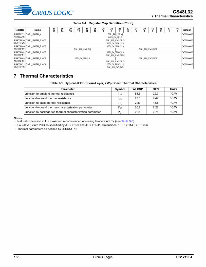
CS48L327 Thermal Characteristics
7 Thermal Characteristics
Notes: • Natural convection at the maximum recommended operating temperature TA (see Table 3-3) • Four-layer, 2s2p PCB as specified by JESD51–9 and JESD51–11; dimensions: 101.5 x 114.5 x 1.6 mm • Thermal parameters as defined by JESD51–12
R58720272 (0x3800010)
DSP1_PMEM_4 DSP1_PM_3 [39:24] 0x00000000DSP1_PM_3 [23:8]
R59006956 (0x3845FEC)
DSP1_PMEM_71675 DSP1_PM_57341 [31:16] 0x00000000DSP1_PM_57341 [15:0]
R59006960 (0x3845FF0)
DSP1_PMEM_71676 DSP1_PM_57342 [23:8] 0x00000000DSP1_PM_57342 [7:0] DSP1_PM_57341 [39:32]
R59006964 (0x3845FF4)
DSP1_PMEM_71677 DSP1_PM_57343 [15:0] 0x00000000DSP1_PM_57342 [39:24]
R59006968 (0x3845FF8)
DSP1_PMEM_71678 DSP1_PM_END [7:0] DSP1_PM_57343 [39:32] 0x00000000DSP1_PM_57343 [31:16]
R59006972 (0x3845FFC)
DSP1_PMEM_71679 DSP1_PM_END [39:24] 0x00000000DSP1_PM_END [23:8]
Table 7-1. Typical JEDEC Four-Layer, 2s2p Board Thermal Characteristics
Parameter Symbol WLCSP QFN Units
Junction-to-ambient thermal resistance JA 55.6 22.3 °C/W
Junction-to-board thermal resistance JB 27.0 7.47 °C/W
Junction-to-case thermal resistance JC 2.83 13.5 °C/W
Junction-to-board thermal-characterization parameter JB 26.7 7.22 °C/W
Junction-to-package-top thermal-characterization parameter JT 0.18 0.78 °C/W
Table 6-1. Register Map Definition (Cont.)
Register Name 31 15
30 14
29 13
28 12
27 11
26 10
25 9
24 8
23 7
22 6
21 5
20 4
19 3
18 2
17 1
16 0 Default
188 Cirrus Logic DS1219F4
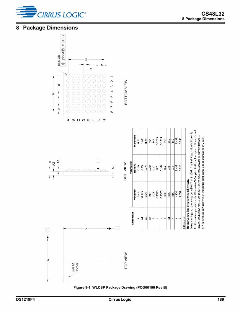
CS48L328 Package Dimensions
8 Package Dimensions
Figure 8-1. WLCSP Package Drawing (POD00106 Rev B)
A2
X
Y
A A1
Ball
A1C
orne
r
M
N
e
e
c
d
SID
E VI
EW
A B C D E F G
67
8
TOP
VIEW
BOTT
OM
VIE
W
H
12
34
5
64X
Øb dd
dC
AB
A3
BOTT
OM
VIE
W
DS1219F4 Cirrus Logic 189

CS48L328 Package Dimensions
Figure 8-2. QFN Package Drawing (ASE Group, 98A0064QN Rev O)
190 Cirrus Logic DS1219F4

CS48L329 Ordering Information
9 Ordering Information
10 Revision History
Table 9-1. Ordering Information
Product Description PackageRoHS
CompliantGrade
TemperatureRange
Container Order #
CS48L32 Low-Power Audio DSP with Microphone Interface
64-ball WLCSP
Yes Commercial –40 to +85°C Tape and Reel 1
1.Reel quantity = 6000 units.
CS48L32-CWZR
CS48L32 Low-Power Audio DSP with Microphone Interface
64-pad QFN Yes Commercial –40 to +85°C Tape and Reel 2
2.Reel quantity = 4000 units.
CS48L32-CNZR
CS48L32 Low-Power Audio DSP with Microphone Interface
64-pad QFN Yes Commercial –40 to +85°C Tray 3
3.Tray quantity = 260 units.
CS48L32-CNZ
Table 10-1. Revision History
Revision Changes
F1
MAR 2019
• SPI2 (QSPI) master interface function description deleted (Section 4.5.5) • SPI1 data-phase control (SPI1_DPHA) added (Table 3-18, Section 4.11, Section 4.11.1) • AUXPDMn_CLK_PD default changed (Table 1-1, Section 4.2.11)
F2
MAR 2019
• SPI1 data-phase control (SPI1_DPHA) default changed to 0 (Section 4.11)
F3
JUN 2019
• Correction to IN1R_SRC field description (Table 4-3) • Deleting erroneous reference to Sleep Mode (Section 4.4.3.1) • Clarification of software-reset conditions (Section 4.4.3.1, Section 4.14.3, Section 4.14.6) • SPI2 (QSPI) master interface function description added (Section 4.5.5)
F4
NOV 2019
• Correction to FLL1_REFCLK_SRC default (Table 4-46).
DS1219F4 Cirrus Logic 191
CS48L3210 Revision History
Contacting Cirrus Logic Support For all product questions and inquiries, contact a Cirrus Logic Sales Representative. To find the one nearest you, go to www.cirrus.com.
IMPORTANT NOTICE
The products and services of Cirrus Logic International (UK) Limited; Cirrus Logic, Inc.; and other companies in the Cirrus Logic group (collectively either “Cirrus Logic” or “Cirrus”) are sold subject to Cirrus Logic’s terms and conditions of sale supplied at the time of order acknowledgment, including those pertaining to warranty, indemnification, and limitation of liability. Software is provided pursuant to applicable license terms. Cirrus Logic reserves the right to make changes to its products and specifications or to discontinue any product or service without notice. Customers should therefore obtain the latest version of relevant information from Cirrus Logic to verify that the information is current and complete. Testing and other quality control techniques are utilized to the extent Cirrus Logic deems necessary. Specific testing of all parameters of each device is not necessarily performed. In order to minimize risks associated with customer applications, the customer must use adequate design and operating safeguards to minimize inherent or procedural hazards. Cirrus Logic is not liable for applications assistance or customer product design. The customer is solely responsible for its product design, including the specific manner in which it uses Cirrus Logic components, and certain uses or product designs may require an intellectual property license from a third party. Customers are responsible for overall system design, and system security. While Cirrus Logic is confident in the performance capabilities of its components, it is not possible to provide an absolute guarantee that they will deliver the outcomes or results envisaged by each of our customers. Features and operations described herein are for illustrative purposes only and do not constitute a suggestion or instruction to adopt a particular product design or a particular mode of operation for a Cirrus Logic component.
CERTAIN APPLICATIONS USING SEMICONDUCTOR PRODUCTS MAY INVOLVE POTENTIAL RISKS OF DEATH, PERSONAL INJURY, OR SEVERE PROPERTY OR ENVIRONMENTAL DAMAGE (“CRITICAL APPLICATIONS”). CIRRUS LOGIC PRODUCTS ARE NOT DESIGNED, AUTHORIZED OR WARRANTED FOR USE IN PRODUCTS SURGICALLY IMPLANTED INTO THE BODY, AUTOMOTIVE SAFETY OR SECURITY DEVICES, NUCLEAR SYSTEMS, LIFE SUPPORT PRODUCTS OR OTHER CRITICAL APPLICATIONS. INCLUSION OF CIRRUS LOGIC PRODUCTS IN SUCH APPLICATIONS IS UNDERSTOOD TO BE FULLY AT THE CUSTOMER’S RISK AND CIRRUS LOGIC DISCLAIMS AND MAKES NO WARRANTY, EXPRESS, STATUTORY OR IMPLIED, INCLUDING THE IMPLIED WARRANTIES OF MERCHANTABILITY AND FITNESS FOR PARTICULAR PURPOSE, WITH REGARD TO ANY CIRRUS LOGIC PRODUCT THAT IS USED IN SUCH A MANNER. IF THE CUSTOMER OR CUSTOMER’S CUSTOMER USES OR PERMITS THE USE OF CIRRUS LOGIC PRODUCTS IN CRITICAL APPLICATIONS, CUSTOMER AGREES, BY SUCH USE, TO FULLY INDEMNIFY CIRRUS LOGIC, ITS OFFICERS, DIRECTORS, EMPLOYEES, DISTRIBUTORS AND OTHER AGENTS FROM ANY AND ALL LIABILITY, INCLUDING ATTORNEYS’ FEES AND COSTS, THAT MAY RESULT FROM OR ARISE IN CONNECTION WITH THESE USES.
This document is the property of Cirrus Logic, and you may not use this document in connection with any legal analysis concerning Cirrus Logic products described herein. No license to any technology or intellectual property right of Cirrus Logic or any third party is granted herein, including but not limited to any patent right, copyright, mask work right, or other intellectual property rights. Any provision or publication of any third party’s products or services does not constitute Cirrus Logic’s approval, license, warranty or endorsement thereof. Cirrus Logic gives consent for copies to be made of the information contained herein only for use within your organization with respect to Cirrus Logic integrated circuits or other products of Cirrus Logic, and only if the reproduction is without alteration and is accompanied by all associated copyright, proprietary and other notices and conditions (including this notice). This consent does not extend to other copying such as copying for general distribution, advertising or promotional purposes, or for creating any work for resale. This document and its information is provided “AS IS” without warranty of any kind (express or implied). All statutory warranties and conditions are excluded to the fullest extent possible. No responsibility is assumed by Cirrus Logic for the use of information herein, including use of this information as the basis for manufacture or sale of any items, or for infringement of patents or other rights of third parties. Cirrus Logic, Cirrus, the Cirrus Logic logo design, and SoundClear are among the trademarks of Cirrus Logic. Other brand and product names may be trademarks or service marks of their respective owners.
Copyright © 2018–2019 Cirrus Logic, Inc. and Cirrus Logic International Semiconductor Ltd. All rights reserved.
SPI is a trademark of Motorola.
192 Cirrus Logic DS1219F4