copyright © infineon technologies 2011. all rights reserved. infineon rd50, liverpool : meeting...
TRANSCRIPT

Copyright © Infineon Technologies 2011. All rights reserved.
Infi
neo
n RD50, Liverpool :Meeting from 23. – 25.05.2011
Werner Schustereder
Some aspects of proton implantation and subsequent thermal annealing

Copyright © Infineon Technologies 2011. All rights reserved. Page 2
Table of Contents
Infineon at a Glance
Business Focus
Divisions, Products and Technology
Some aspects of proton implantation and thermal annealing
03/05/2011
Copyright © Infineon Technologies 2011. All rights reserved. Page 304/28/2010 Page 3
Company PresentationMay 23, 2011
Copyright © Infineon Technologies 2011. All rights reserved. Page 4
Table of Contents
Infineon at a Glance
Business Focus
Divisions, Products and Technology
Some aspects of proton implantation and thermal annealing
03/05/2011

Copyright © Infineon Technologies 2011. All rights reserved.
Infineon at a Glance
The Company
Infineon provides semiconductor and system solutions, focusing on three central needs of our modern society:Energy Efficiency, Mobility and Security
Revenue in FY 2010*: 3.295 billion EUR
25,119 employees worldwide (as of April 2011)
Strong technology portfolio with about 15,400 patents and patent applications (as of Feb. 2011)
More than 20 R&D locations
Germany’s largest semiconductor company
*Note: Figures according to IFRS with Wireline and Wireless as discontinued operations; as of September 30, 2010
03/05/2011 Page 5
Copyright © Infineon Technologies 2010. All rights reserved. Page 6
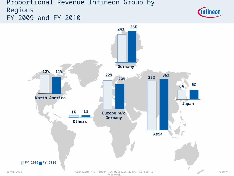
Proportional Revenue Infineon Group by RegionsFY 2009 and FY 2010
Germany
24% 26%
North America
12% 11%
Others
1% 1% Europe w/oGermany
22%20%
Asia
35% 36%
Japan
6% 6%
FY 2009 FY 2010
03/05/2011
Copyright © Infineon Technologies 2010. All rights reserved. Page 7
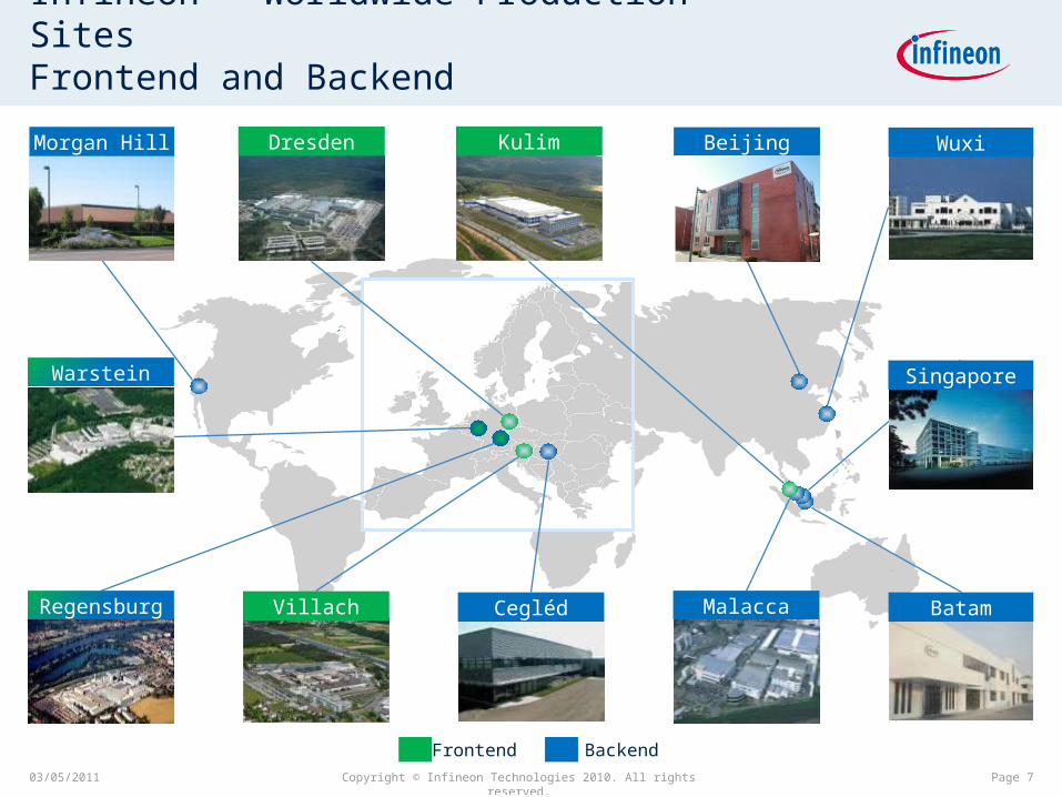
Infineon – Worldwide Production Sites Frontend and Backend
VillachRegensburg
Singapore
Batam
WuxiDresden Kulim
Cegléd
Warstein
Malacca
Morgan Hill
Frontend Backend
Beijing
03/05/2011
Copyright © Infineon Technologies 2010. All rights reserved. Page 8
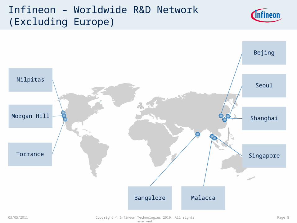
Infineon – Worldwide R&D Network (Excluding Europe)
Bejing
Bangalore
Singapore
Malacca
Milpitas
Morgan Hill
Torrance
Shanghai
Seoul
03/05/2011

Copyright © Infineon Technologies 2010. All rights reserved. Page 9
Infineon – R&D Network in Europe
Duisburg Warstein
Augsburg
Bristol
Dresden
Munich,Neubiberg
Regens-burg
Graz
VillachPadova Bucharest
Linz
03/05/2011
Copyright © Infineon Technologies 2011. All rights reserved. Page 10
Table of Contents
Infineon at a Glance
Business Focus
Divisions, Products and Technology
Some aspects of proton implantation and thermal annealing
03/05/2011
Copyright © Infineon Technologies 2010. All rights reserved. Page 11
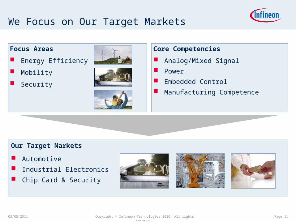
We Focus on Our Target Markets
Core Competencies
Analog/Mixed Signal Power Embedded Control Manufacturing Competence
Focus Areas
Energy Efficiency
Mobility
Security
Our Target Markets
Automotive Industrial Electronics Chip Card & Security
03/05/2011
Copyright © Infineon Technologies 2010. All rights reserved.
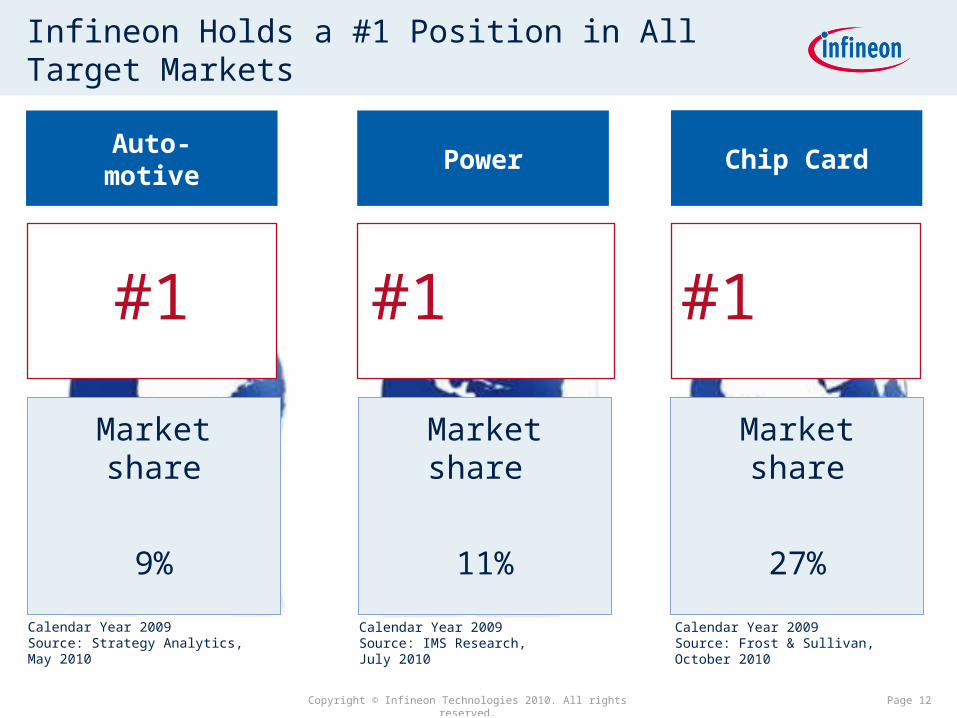
Infineon Holds a #1 Position in All Target Markets
#1
Power
Marketshare
11%
Chip Card
#1
Marketshare
27%
Auto-motive
#1
Marketshare
9%
Calendar Year 2009Source: IMS Research,July 2010
Calendar Year 2009Source: Frost & Sullivan,October 2010
Calendar Year 2009Source: Strategy Analytics,May 2010
Page 12
Copyright © Infineon Technologies 2011. All rights reserved. Page 13
Table of Contents
Infineon at a Glance
Business Focus
Divisions, Products and Technology
Some aspects of proton implantation and thermal annealing
03/05/2011
Copyright © Infineon Technologies 2011. All rights reserved. Page 14
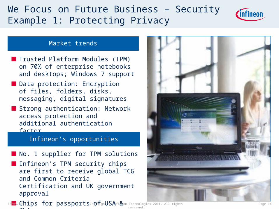
We Focus on Future Business – Security Example 1: Protecting Privacy
■ Trusted Platform Modules (TPM) on 70% of enterprise notebooks and desktops; Windows 7 support
■ Data protection: Encryption of files, folders, disks, messaging, digital signatures
■ Strong authentication: Network access protection and additional authentication factor
■ No. 1 supplier for TPM solutions
■ Infineon's TPM security chips are first to receive global TCG and Common Criteria Certification and UK government approval
■ Chips for passports of USA & China
Market trends
Infineon's opportunities
03/05/2011
Copyright © Infineon Technologies 2011. All rights reserved.03/05/2011
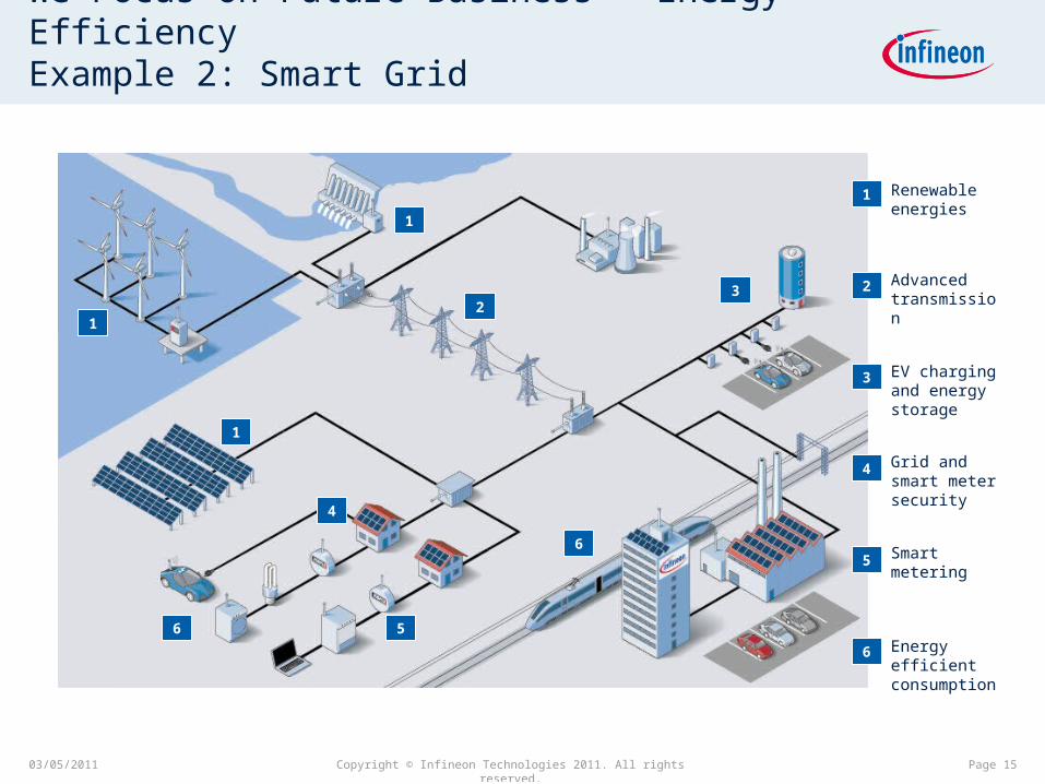
Renewable energies
12
3
4
1
Advanced transmission
2
EV charging and energy storage
3
Grid and smart meter security
4
Smart metering
5
Energy efficient consumption
6
6
6
1
5
1
We Focus on Future Business – Energy EfficiencyExample 2: Smart Grid
Page 15

Copyright © Infineon Technologies 2011. All rights reserved. Page 16
We Focus on Future Business – Mobility Example 3: Making Cars Cleaner
Market trends
■ Dwindling energy resources
■ Stricter CO2 emission legislations
■ Growing environmental awareness
Infineon's opportunities
■ Infineon components are key for CO2 reduction: Total improvement of
CO2-emission ~23 g/km
■ We offer Hybrid and electric drivetrain products (HybridPACK™)
■ No electric vehicle without semiconductors: electric drive and control, battery management, on-board battery charging and power grid communication
Note: Baseline CO2 reduction in g/km: 170 g/km on Ø EU cars
03/05/2011
Copyright © Infineon Technologies 2011. All rights reserved. Page 17
Table of Contents
Market and Business Development 2nd Quarter Fiscal Year 2011
Business Focus
Divisions, Products and Technology
Some aspects of proton implantation and thermal annealing
03/05/2011
Copyright © Infineon Technologies 2011. All rights reserved. Page 18
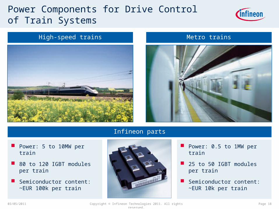
Power Components for Drive Control of Train Systems
Power: 0.5 to 1MW per train
25 to 50 IGBT modules per train
Semiconductor content:~EUR 10k per train
Infineon parts
Metro trainsHigh-speed trains
Power: 5 to 10MW per train
80 to 120 IGBT modules per train
Semiconductor content:~EUR 100k per train
03/05/2011

Copyright © Infineon Technologies 2011. All rights reserved.
Concept of IGBT – rough overview
Logic on front side of chip
Source – Drain in 3D to allow switching of kV
Suitable raw material and processing essential for excellent device characteristics
Low dark currents
High and stable break through voltage
Fast soft switching with minimal losses
…
Several approaches to optimize processes in Si, one of them:
proton implantation in Si

Copyright © Infineon Technologies 2011. All rights reserved.
Points of contact(charged) particle interaction with Si
CMS detectors: ~1014 – 1016 particles cm-2 / 10 years
Degradation of detectors – radiation hardness
Investigate underlaying physical processes
¬ Conversion from n-type to p-type Si
¬ Which types of defects are formed, what can be done about it?
¬ Investigate influence of raw material ((DO)FZ, (m)CZ, [O(i)], …)
¬ …
Infineon: ~1012 – 1015 particles cm-2 @ every chip within ~50µm
Try to use initial defects of proton implantation
¬ Fact: thermal treatment especially @ 350 – 500°C converts
p-type n-type material, but why & how?

Copyright © Infineon Technologies 2011. All rights reserved.
Points of contact(charged) particle interaction with Si
CMS detectors: ~1014 – 1016 particles cm-2 / 10 years
Degradation of detectors – radiation hardness
Investigate underlaying physical processes…
¬ Conversion from n-type to p-type Si
¬ Which types of defects are formed, what can be done about it?
¬ Investigate influence of raw material ((DO)FZ, (m)CZ, [O(i)], …)
¬ …
Infineon: ~1012 – 1015 particles cm-2 @ every chip within ~50µm
Try to use initial defects of proton implantation
¬ Fact: thermal treatment especially @ 350 – 500°C converts
p-type n-type material, but why & how?
Investigate underlaying physical processes…
Copyright © Infineon Technologies 2011. All rights reserved.
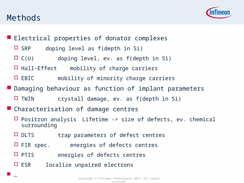
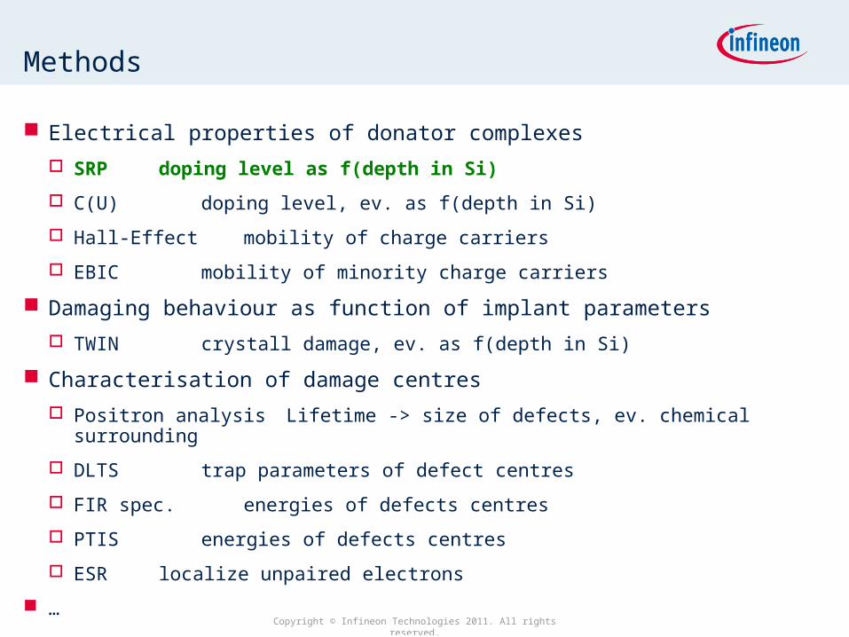
Methods
Electrical properties of donator complexes
SRP doping level as f(depth in Si)
C(U) doping level, ev. as f(depth in Si)
Hall-Effect mobility of charge carriers
EBIC mobility of minority charge carriers
Damaging behaviour as function of implant parameters
TWIN crystall damage, ev. as f(depth in Si)
Characterisation of damage centres
Positron analysis Lifetime -> size of defects, ev. chemical surrounding
DLTS trap parameters of defect centres
FIR spec. energies of defects centres
PTIS energies of defects centres
ESR localize unpaired electrons
…
Copyright © Infineon Technologies 2011. All rights reserved.
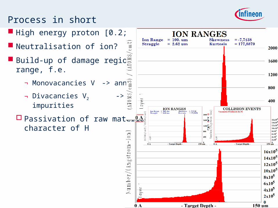
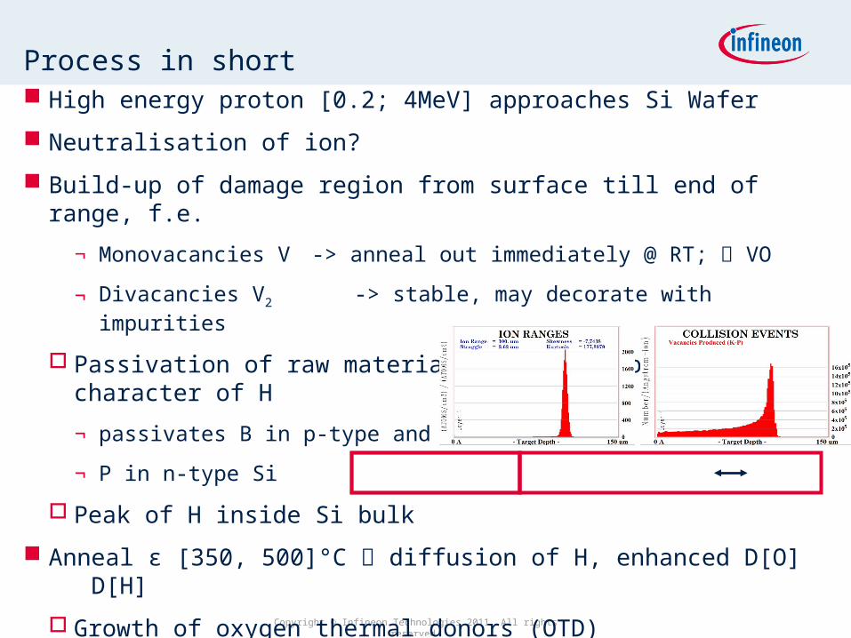
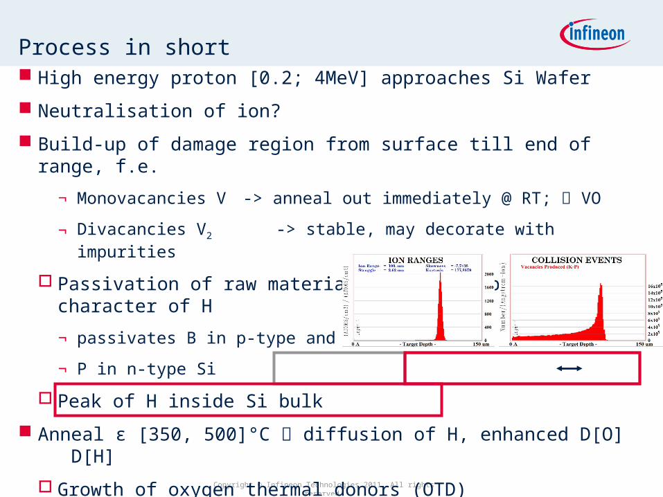
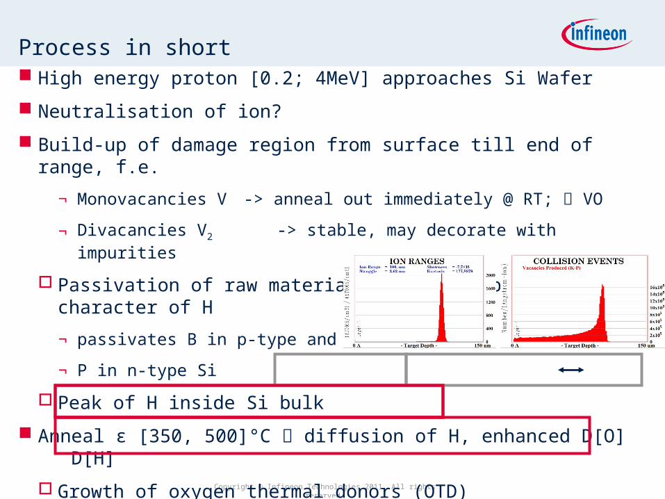
Process in short High energy proton [0.2; 4MeV] approaches Si Wafer
Neutralisation of ion?
Build-up of damage region from surface till end of range, f.e.
¬ Monovacancies V -> anneal out immediately @ RT; VO
¬ Divacancies V2 -> stable, may decorate with impurities
Passivation of raw material doping – amphoteric character of H
¬ passivates B in p-type and also
¬ P in n-type Si
Peak of H inside Si bulk
Anneal ε [350, 500]°C diffusion of H, enhanced D[O] D[H]
Growth of oxygen thermal donors (OTD)
Creation of different types as f(Temp.) of hydrogen donors
Carrier concentration after anneal ~1% of implanted H dose
Copyright © Infineon Technologies 2011. All rights reserved.
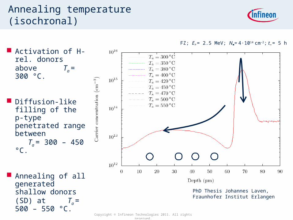
Annealing temperature (isochronal)
Activation of H-rel. donors above Ta = 300 °C.
Diffusion-like filling of the p-type penetrated range between Ta
= 300 – 450 °C.
Annealing of all generated shallow donors (SD) at Ta = 500 – 550 °C.
FZ; EP = 2.5 MeV; N■= 4·1014 cm-2; ta = 5 h
PhD Thesis Johannes Laven, Fraunhofer Institut Erlangen
Copyright © Infineon Technologies 2011. All rights reserved.
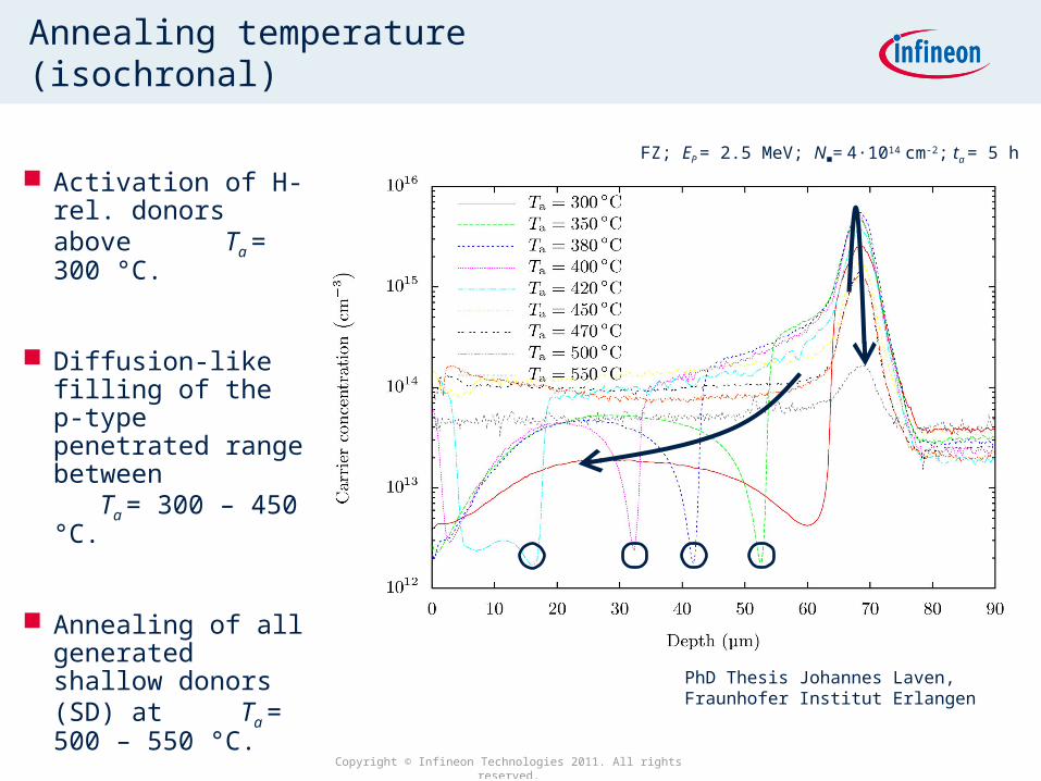
FZ; EP = 2.5 MeV; N■= 4·1014 cm-2; ta = 5 h
Annealing temperature (isochronal)
Activation of H-rel. donors above Ta = 300 °C.
Diffusion-like filling of the p-type penetrated range between Ta
= 300 – 450 °C.
Annealing of all generated shallow donors (SD) at Ta = 500 – 550 °C.
PhD Thesis Johannes Laven, Fraunhofer Institut Erlangen
Copyright © Infineon Technologies 2011. All rights reserved.
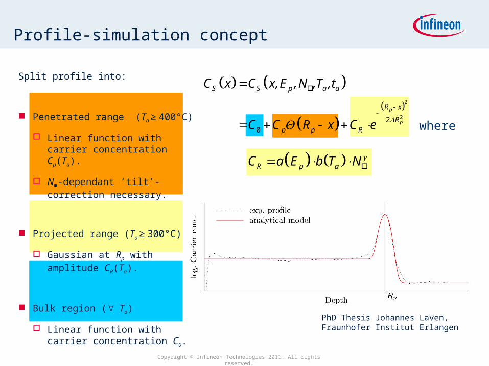
Split profile into:
Penetrated range (Ta ≥ 400°C)
Linear function with carrier concentration Cp(Ta).
N■-dependant ‘tilt’-correction necessary.
Projected range (Ta ≥ 300°C)
Gaussian at Rp with amplitude CR(Ta).
Bulk region ( Ta)
Linear function with carrier concentration C0.
2
220
p
p
S S p a a
R x
Rp p R
C x C x,E ,N ,T ,t
C C R x C e
Profile-simulation concept
R p aC a E b T N
where
PhD Thesis Johannes Laven, Fraunhofer Institut Erlangen

Copyright © Infineon Technologies 2011. All rights reserved.
H diffusion in Si [Pearton]
p-type Si: hydrogen present as H+;
rapid diffusion (~1010cm-2s-1 @ RT)
T < 500°C: diff. impeded by trapping at acceptor ions
T > 500°C: diff. by rapid interstitial motion
n-type Si: H+ and H0, depending on dopant density
D[H] considerably much lower compared to p-type Si
T < 150°C: donor-Si-H bonds can form impeding H motion & passivating donors
Molecule formation can occur
H2 much less mobile than atomic species and generally breaks up rather than diffuse
D[H2] in n-type > D[H2] in p-type
Copyright © Infineon Technologies 2011. All rights reserved.
Process in short High energy proton [0.2; 4MeV] approaches Si Wafer
Neutralisation of ion?
Build-up of damage region from surface till end of range, f.e.
¬ Monovacancies V -> anneal out immediately @ RT; VO
¬ Divacancies V2 -> stable, may decorate with impurities
Passivation of raw material doping – amphoteric character of H
¬ passivates B in p-type and also
¬ P in n-type Si
Peak of H inside Si bulk
Anneal ε [350, 500]°C diffusion of H, enhanced D[O] D[H]
Growth of oxygen thermal donors (OTD)
Creation of different types as f(Temp.) of hydrogen donors
Carrier concentration after anneal ~1% of implanted H dose
Copyright © Infineon Technologies 2011. All rights reserved.
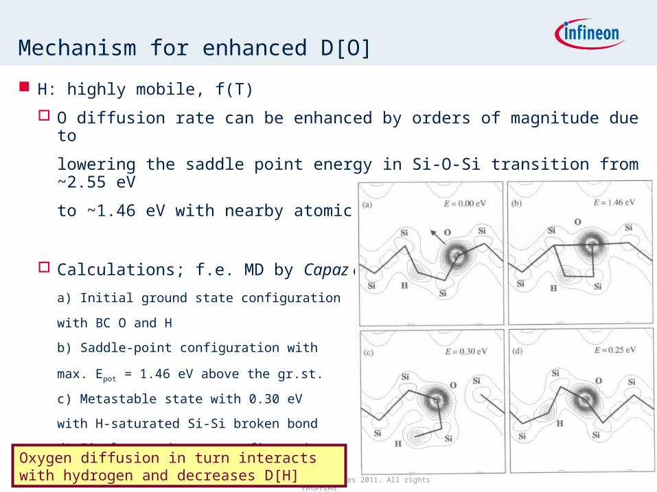
Mechanism for enhanced D[O]
H: highly mobile, f(T)
O diffusion rate can be enhanced by orders of magnitude due to
lowering the saddle point energy in Si-O-Si transition from ~2.55 eV
to ~1.46 eV with nearby atomic H
Calculations; f.e. MD by Capaz et al.
a) Initial ground state configuration
with BC O and H
b) Saddle-point configuration with
max. Epot = 1.46 eV above the gr.st.
c) Metastable state with 0.30 eV
with H-saturated Si-Si broken bond
d) Final ground-state configuration
with BC O and H
A true ground-state can be obtained by
rotations of H and O along the Si-Si axes.
Oxygen diffusion in turn interacts with hydrogen and decreases D[H]
Copyright © Infineon Technologies 2011. All rights reserved.
Process in short High energy proton [0.2; 4MeV] approaches Si Wafer
Neutralisation of ion?
Build-up of damage region from surface till end of range, f.e.
¬ Monovacancies V -> anneal out immediately @ RT; VO
¬ Divacancies V2 -> stable, may decorate with impurities
Passivation of raw material doping – amphoteric character of H
¬ passivates B in p-type and also
¬ P in n-type Si
Peak of H inside Si bulk
Anneal ε [350, 500]°C diffusion of H, enhanced D[O] D[H]
Growth of oxygen thermal donors (OTD)
Creation of different types as f(Temp.) of hydrogen donors
Carrier concentration after anneal ~1% of implanted H dose

Copyright © Infineon Technologies 2011. All rights reserved.
Configurations of Oi in Si Oxygen thermal donors (OTD)
Formation of OTD: Si O
electrical inactive: electrical active ring structure:
Growth of ring structure, up to ~ 8 O atoms involved:
Rings with more than 8 O atoms are electrically inactive
Concurring structure: “di-Y-lid“, also el. inactive
Copyright © Infineon Technologies 2011. All rights reserved.
Process in short High energy proton [0.2; 4MeV] approaches Si Wafer
Neutralisation of ion?
Build-up of damage region from surface till end of range, f.e.
¬ Monovacancies V -> anneal out immediately @ RT; VO
¬ Divacancies V2 -> stable, may decorate with impurities
Passivation of raw material doping – amphoteric character of H
¬ passivates B in p-type and also
¬ P in n-type Si
Peak of H inside Si bulk
Anneal ε [350, 500]°C diffusion of H, enhanced D[O] D[H]
Growth of oxygen thermal donors (OTD)
Creation of different types as f(Temp.) of hydrogen donors
Carrier concentration after anneal ~1% of implanted H dose

Copyright © Infineon Technologies 2011. All rights reserved.
Different types Hydrogen Donors (HD)
HD(I)
[CiOi-H]-Complex?
H-related shallow donors:
HD(II)
IR absorption spectra are similar to TDDs
Spectra differ under stress
I-rel. extended defects?
- E0/+: EC - 66 meV *
E++/+: EC - 100 meV *
HD(III)
IR absorption spectra show Si-H vibrations with identical annealing behavior
Multiple levels
- EC - (35 – 44) meV **
EC - (26 – 53) meV
*: Mukashev et al, 1985
**: Hartung and Weber, 1993
Abdullin et al, 2004
Markevichetal, 1998
OTD
Also literature reports on 3 different types of donors; e.g. Tokuda et al., Hatakeyama et al.
Copyright © Infineon Technologies 2011. All rights reserved.
Creation of Hydrogen Donors (HD)
Fact: concentration of donors ~1% of implanted H
Open questions
¬ Correlation (Transition?) of STD with OTD unclear
¬ Correlation of STD with O concentration [also Lit: f.e. Navarro]
¬ Possible complex influence of N concentration [Hartung]
¬ Role of C unclear
Fact: 7 different energy levels with BE 34-53meV [Hartung PR B48]
Open questions
¬ ev. N-O-complexes as STD [Suezawa, Thewalt, Yang]
¬ Ci-H-2Oi as electrically active STD core possible (below ~300°C ?)
¬ Vi-Hi-Oi as electrically active STD core possible (above ~300°C ?)
STD -> microscopic structure unclear

Copyright © Infineon Technologies 2011. All rights reserved.
Influence of raw material: FZ vs. mCZ
Surface:
N◘-dependency more pronounced in mCZ
Penetrated range:
FZ: stays longer @ p-type for lower Temps / shorter annealing times
mCZ: shows higher resistance values for lower Temps / shorter annealing times
Shoulder:
in FZ only visible for very high N◘
EP = 2.5 MeV; Ta = 470 °C; ta = 5 h
PhD Thesis Johannes Laven, Fraunhofer Institut ErlangenFurthermore: Carrier concentration
non-linear with proton dose > ~4E14

Copyright © Infineon Technologies 2011. All rights reserved.
Summary
Some CC profiles of proton implanted Silicon have been shown
Dependencies examined are mainly
Ep= 0.5 – 4.0 MeV N◘ ~ 1013 – 1015 cm-2
Ta = 300 – 550 °C ta = 0.5 – 30 h
Some lessons learned are
Diffusion of hydrogen is trap-limited and f(Temp., time)
Vacancies, hydrogen and oxygen interact diffusion coefficient
3 different types of HD seem to exist
Nature of OTD seems understood, but not all aspects completely clear
Sublinear donor dependency with implanted dose > ~4E14
Effect of raw material substrates obvious, but not understood
Effort to compile a CC profile simulation concept is ongoing using
A stationary radiation damage-related species
A diffusing species
Copyright © Infineon Technologies 2011. All rights reserved.
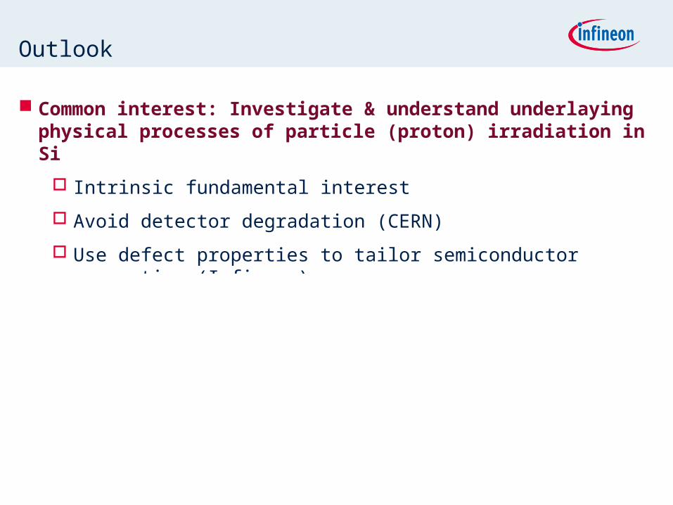
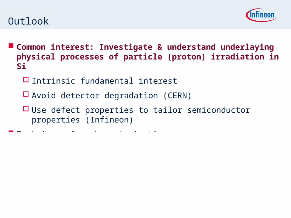
Outlook
Common interest: Investigate & understand underlaying physical processes of particle (proton) irradiation in Si
Intrinsic fundamental interest
Avoid detector degradation (CERN)
Use defect properties to tailor semiconductor properties (Infineon)
Techniques for characterisation
Copyright © Infineon Technologies 2011. All rights reserved.
Methods
Electrical properties of donator complexes
SRP doping level as f(depth in Si)
C(U) doping level, ev. as f(depth in Si)
Hall-Effect mobility of charge carriers
EBIC mobility of minority charge carriers
Damaging behaviour as function of implant parameters
TWIN crystall damage, ev. as f(depth in Si)
Characterisation of damage centres
Positron analysis Lifetime -> size of defects, ev. chemical surrounding
DLTS trap parameters of defect centres
FIR spec. energies of defects centres
PTIS energies of defects centres
ESR localize unpaired electrons
…
Copyright © Infineon Technologies 2011. All rights reserved.
Outlook
Common interest: Investigate & understand underlaying physical processes of particle (proton) irradiation in Si
Intrinsic fundamental interest
Avoid detector degradation (CERN)
Use defect properties to tailor semiconductor properties (Infineon)
Techniques for characterisation
Learn from each other, new ideas?
Exchange & combine knowledge
Collaborate in certain experiments
Eventually effort on quantum-chem. calculations of defects in Si
…
