rd50 status report
TRANSCRIPT
RD50 Status Report- September 2020 –
Radiation hard semiconductor devices
for very high luminosity colliders
RD50 Status Report 2020 - LHCC 02/09/2020
• RD50 Collaboration
• Scientific results 2019/20 (highlights)• Defect and Material Characterization
• Detector Characterization
• New Detector Structures
• Full Detector Systems
• Spares
• RD50 - 5 Year Work Plan (Status of Milestones)
• Outlook
Discussion with LHCC referee – 26.8.2020
Outline:
26 August 2020 1

RD50 Motivation and ChallengeSilicon detectors upgrades and operation
- Radiation Hardness -
• LHC operation
• HL-LHC (High Luminosity LHC)
• detector developments for HL-LHC
• starting after LS3 (~2024-26);
• expect 4000 fb-1 (nominal LHC was 300 fb-1)
• HL-LHC operation & upgrades
• operation of HL-LHC
• damage modelling, evaluation, mitigation
• ATLAS Pixel replacement, LHCb upgrade, …
• FCC – Future Circular Collider
26 August 2020 RD50 Status Report 2020 - LHCC 02/09/2020 2
• Increasing radiation levels
• Semiconductor detectors will face >1016 neq/cm2 (HL-LHC) and >7x10¹⁷ neq/cm2 (FCC-hh)
detectors used at LHC cannot be operated after such irradiation
• New requirement and new detector technologies
• New requirements or opportunities lead to new technologies (e.g. HV-CMOS, LGAD,…)
which need to be evaluated and optimized in terms of radiation hardness
[I. D
aw
so
n,
P. S
. M
iya
ga
wa
, S
he
ffie
ld U
niv
ers
ity, A
tla
s]

The RD50 Collaboration• RD50: 64 institutes and 403 members
26 August 2020 RD50 Status Report 2020 - LHCC 02/09/2020 3
51 European institutesAustria (HEPHY), Belarus (Minsk), Czech Republic (Prague (3x)), Finland (Helsinki,
Lappeenranta ), France (Marseille, Paris, Orsay), Germany (Bonn, Dortmund, Freiburg,
Göttingen, Hamburg (2x), Karlsruhe, Munich(2x)), Greece (Demokritos), Italy (Bari,
Perugia, Pisa, Trento, Torino), Croatia (Zagreb), Lithuania (Vilnius), Montenegro
(Montenegro), Netherlands (NIKHEF), Poland (Krakow), Romania (Bucharest), Russia
(Moscow, St.Petersburg), Slovenia (Ljubljana), Spain (Barcelona(3x), Santander, Sevilla
(2x), Valencia), Switzerland (CERN, PSI, Zurich), United Kingdom (Birmingham,
Glasgow, Lancaster, Liverpool, Oxford, Manchester, RAL)
8 North-American institutesCanada (Ottawa), USA (BNL, Brown Uni, Fermilab,
LBNL, New Mexico, Santa Cruz, Syracuse)
1 Middle East instituteIsrael (Tel Aviv)
4 Asian institutes China (Beijing-IHEP, Hefei, Jilin), India (Delhi)
4 new members since September 2019
Full member list: www.cern.ch/rd50
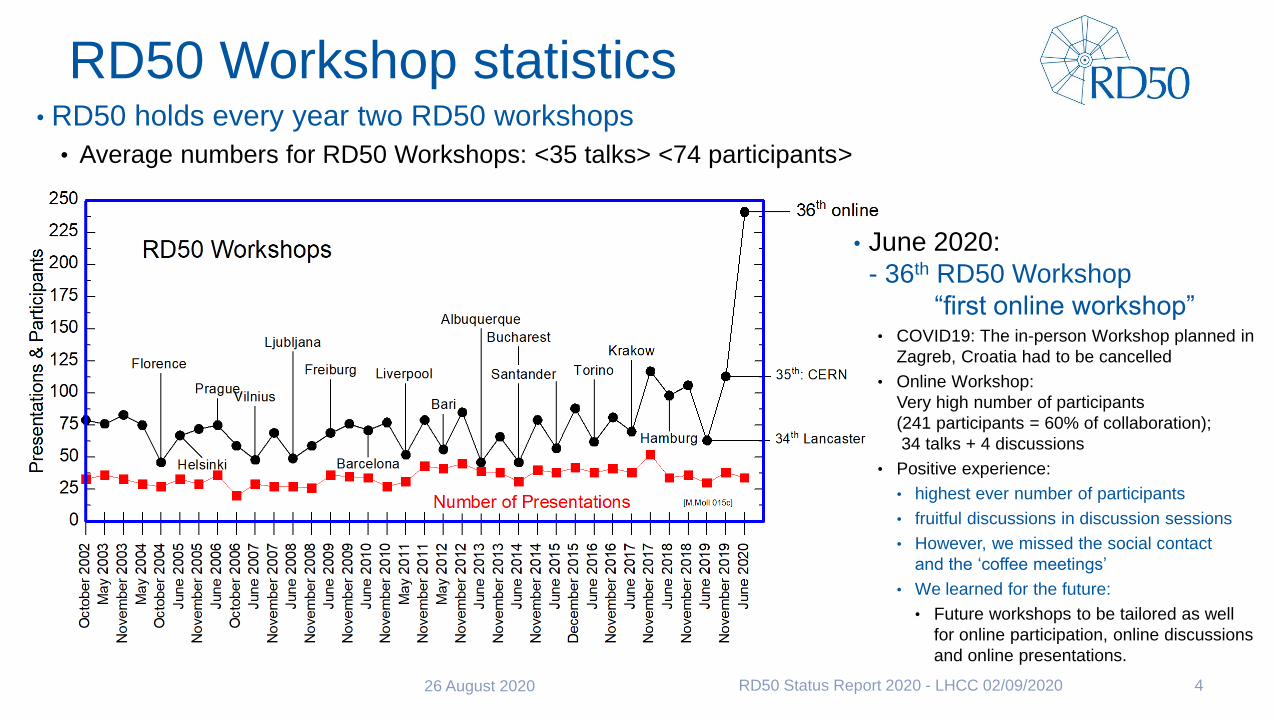
RD50 Workshop statistics
26 August 2020 RD50 Status Report 2020 - LHCC 02/09/2020 4
• RD50 holds every year two RD50 workshops
• Average numbers for RD50 Workshops: <35 talks> <74 participants>
• June 2020:
- 36th RD50 Workshop
“first online workshop”• COVID19: The in-person Workshop planned in
Zagreb, Croatia had to be cancelled
• Online Workshop:
Very high number of participants
(241 participants = 60% of collaboration);
34 talks + 4 discussions
• Positive experience:
• highest ever number of participants
• fruitful discussions in discussion sessions
• However, we missed the social contact
and the ‘coffee meetings’
• We learned for the future:
• Future workshops to be tailored as well
for online participation, online discussions
and online presentations.

RD50 Organizational Structure
26 August 2020 RD50 Status Report 2020 - LHCC 02/09/2020 5
Co-Spokespersons
Gianluigi Casse and Michael Moll(Liverpool University, UK (CERN EP-DT)
& FBK-CMM, Trento, Italy)
Defect / Material
CharacterizationIoana Pintilie
(NIMP Bucharest)
Detector
CharacterizationEckhart Fretwurst(Hamburg University)
Full Detector
SystemsGregor Kramberger
(Ljubljana University)
• Characterization of
microscopic properties
of standard-, defect
engineered and new materials;
pre- and post- irradiation
• DLTS, TSC, ….
• SIMS, SR, …
• NIEL (calculations)
• Cluster and point defects
• Boron related defects
• SiC based detectors
•Characterization of test
structures (IV, CV, CCE, TCT,.)
•Development and testing of
defect engineered devices
•EPI, MCZ and other materials
•NIEL (experimental)
•Device modeling
•Operational conditions
•Common irradiations
• Wafer procurement (M.Moll)
• Acceptor removal (Kramberger)
• TCAD modeling (J.Schwandt)
• 3D detectors
• Thin detectors
• Cost effective solutions
• Other new structures
• Detectors with internal gain
• LGAD:Low Gain Avalanche Det.
• Deep Depleted Avalanche Det.
• Slim Edges
• HVCMOS
• LGAD (S.Hidalgo)
• HVCMOS (E. Vilella)
• LHC-like tests
• Links to HEP (LHC P2, FCC)
• Links electronics R&D
• Low rho strips
• Sensor readout (Alibava)
• Comparison:
- pad-mini-full detectors
- different producers
•Radiation Damage in
HEP detectors
•Timing detectors
•Test beams
(M.Bomben & G.Casse)
New Structures
Giulio Pellegrini (CNM Barcelona)
Collaboration Board Chair & Deputy: G.Kramberger (Ljubljana) & J.Vaitkus (Vilnius), Conference committee: U.Parzefall (Freiburg)
CERN contact: M.Moll (EP-DT), Secretary: V.Wedlake (EP-DT), Budget holder: M.Moll & M.Glaser (EP-DT) , EXSO: R.Costanzi (EP-DT)
• Organizational
structure not changed

Defect & Material
Characterization
Recent results 2019/20
26 August 2020 RD50 Status Report 2020 - LHCC 02/09/2020 6

Defect Characterization• Aim of defect studies:
• Identify defects responsible for Change of Neff ,
Change of E-Field, Trapping, Leakage Current
• Understand if knowledge can be used to mitigate
radiation damage (e.g. defect engineering)
• Deliver input for device simulations to predict
detector performance under various conditions
• Method: Defect Analysis performed with various tools
• DLTS (Deep Level Transient Spectroscopy)
• TSC (Thermally Stimulated Currents)
• PITS (Photo Induced Transient Spectroscopy)
• FTIR (Fourier Transform Infrared Spectroscopy)
• EPR (Electron Paramagnetic Resonance)
• TCT (Transient Current Technique)
• CV/IV (Capacitance/Current-Voltage Measurement)
• MW-PC (Microwave Probed Photo Conductivity)
• PC, RL, I-DLTS, TEM,… and simulations
• RD50: several hundred samples irradiated with protons, neutrons, electrons and 60Co-g
26 August 2020 RD50 Status Report 2020 - LHCC 02/09/2020 7
space charge trapping leakage current
[E.F
retw
urs
te
t a
l. –
RD
50
No
v.2
01
8]

Radiation induced defects with
impact on device performance
26 August 2020 RD50 Status Report 2020 - LHCC 02/09/2020 8
RD50 map of most relevant defects for device performance near room temperature:
BiOi(acceptor removal)
Phosphorus: shallow dopant(positive charge)
BD: positive charge higher introduction after proton than after
neutron irradiation, oxygen dependent
E30: positive charge
higher introduction after
proton irradiation than after
neutron irradiation
Leakage
current: V3
Reverse
annealing(negative charge)
Boron: shallow dopant(negative charge)
leakage current
& neg. chargecurrent after g irrad,
V2O (?)
• Trapping: Indications that E205a and H152K are important (further work needed)
• Converging on consistent set of defects observed after p, p, n, g and e irradiation.
• Defect introduction rates are depending on particle type and energy, and some on material!

• Acceptor removal coefficients obtained on a wide range of sensor types
• pin diodes (epi, FZ, MCZ, …), LGAD detectors, CMOS sensors
• after charged hadron irradiation (red) and neutron irradiation (black/blue)
26 August 2020 RD50 Status Report 2020 - LHCC 02/09/2020 9
𝑁𝑒𝑓𝑓 Φ = NB0 exp −𝑐𝐴Φ + 𝑔 ⋅ Φ
• Parameterization of acceptor removal established within RD50
• covering the range [B]=1012 to 1018 cm-3 (10 kWcm to 5 mWcm) i.e. damage predictions can be done
Example: 23 GeV proton irradiated epi diodes
[M.M
oll
–P
oS
(Vert
ex2019)0
27]
• Acceptor removal: Radiation induced de-activation of acceptors (p-type doping, Boron)
• Impact:
• Macroscopic studies:
• Change of silicon conductivity; Change of sensor depletion voltage and/or active volume
• Loss of gain in LGAD sensors, sets radiation harness limits for timing detectors (ETL, HGTD)
RD50: Dedicated acceptor removal studies

BiOi
Defect studies: Acceptor Removal• Microscopic origin:
• Formation of defects containing Boron that no longer acts as shallow dopant
26 August 2020 RD50 Status Report 2020 - LHCC 02/09/2020 10
Bs
Radiation
Damage
• Status
• Large amount of data (Wafers, Detectors, CMOS, LGAD)
• Acceptor removal is parametrized over 6 orders of magnitude in resistivity
• Damage predictions are possible
• Defect engineering (with Carbon) works
but microscopic understanding needs more work!
• Measured defect concentrations do not fully explain the macroscopic observations.
50 100 150 2000
10
20
30
V2 in clusters
H(152)
H(140)
H(116)
BiOi
VOi+CiOi
IO2
H(40)
TS
C s
ign
al (p
A)
Temperature (K)
neutrons, 3.3E+14
protons, 3.3E+14
E(30)
EPI p-type Si, 250 Wcm

Detector Characterization
Recent results 2019/20
26 August 2020 RD50 Status Report 2020 - LHCC 02/09/2020 11

Transient Current Technique (TCT)
• Pulsed laser induced generation of charge carriers inside detector• Study of: electric field in sensor, charge collection efficiency, homogeneity,..
• Benchmark simulation tools, measure physics parameters from mobility to impact ionization
• New TCT technology: TPA-TCT – Two Photon Absorption TCT
26 August 2020 RD50 Status Report 2020 - LHCC 02/09/2020 12
• TCT (red laser)• short penetration length (650nm = 1.9eV)
• carriers deposited in a few mm from surface
• front and back TCT: study electron and hole drift separately
• 2D spatial resolution (5-10mm)
• TCT (infrared laser)• long penetration (1064nm = 1.17 eV)
• similar to MIPs (though different dE/dx)
• top and edge-TCT
• 2D spatial resolution (5-10mm)
• TPA-TCT (far infrared)• No single photon absorption in silicon
• 2 photons produce one electron-hole pair
• Point-like energy deposition in focal point
• 3D spatial resolution (1 x 1 x 10 mm3)
edge-TCT invented
within RD50: 2010
Table-top
TPA-TCT system

Table-top TPA-TCT system• Development of a customized fiber-laser (1550 nm, ~ 200 fs) with external company (Seed funding: CERN KT-Fund grant)
• 2019/20 proof of concept achieved at CERN & commercialization started
• 2020: 2nd laser installed at IFCA, Santander, Spain, … system optimization and development ongoing
26 August 2020 RD50 Status Report 2020 - LHCC 02/09/2020 13
• Characterization of un-/irradiated silicon sensors
• charge generation only at focal point
• very good spatial resolution (1 x 1 x 10 mm3)
• 3D mapping of sensors possible
200µm
Si: Single Photon absorption z-scan measurement at CERN
no absorption unless two photons
are absorbed at same time (within fs)
𝑑𝐼(𝑟, 𝑧)
𝑑𝑡= − 𝛼𝐼 − 𝛽𝐼2(𝑟, 𝑧)
charge carrier density Commercialization (2020)
• LPS: Laser Pulse Source
• All-fiber CPA fs pulses generation
• Pulse rep. single shot to 8 MHz
• LPM: Laser Pulse Management
• Pulse energy: <10 pJ to > 10 nJ
• Synchronized shutter.
rise/fall time < 1 us
• D-SCAN: Dispersion scanning
• Pulse duration: 200 fs to 500 fs
• Spectral and temporal
pulse characterization
[P.P
ere
z-M
illan,
Fyla
–R
D5
0 W
ork
sh
op
6/2
02
0]
[M.W
ieh
e, R
D50 W
ork
shop 6
/20
20]
no SPA TPA

Studying Trapping/Detrapping by TCT
Concept: Use subsequent TCT laser
pulses to inject charge carriers into
irradiated silicon sensors and study the
trapping and detrapping from defect
levels by analyzing the TCT signal.
26 August 2020 RD50 Status Report 2020 - LHCC 02/09/2020 14
Voltage: 70V
Example: p-type sensor, neutron irradiated (1015 neq/cm2)
• variation of delay between TCT pulses
Conclusion:
• Trapping has significant impact on TCT signals (as function of
repetition frequency, laser intensity, temperature, voltage, ….)
• Excellent dataset for benchmark of sensor simulations
• Extraction of trapping/detrapping parameters possible
[L.Diehl, Freiburg – 36th RD50 Workshop 6/2020]
15
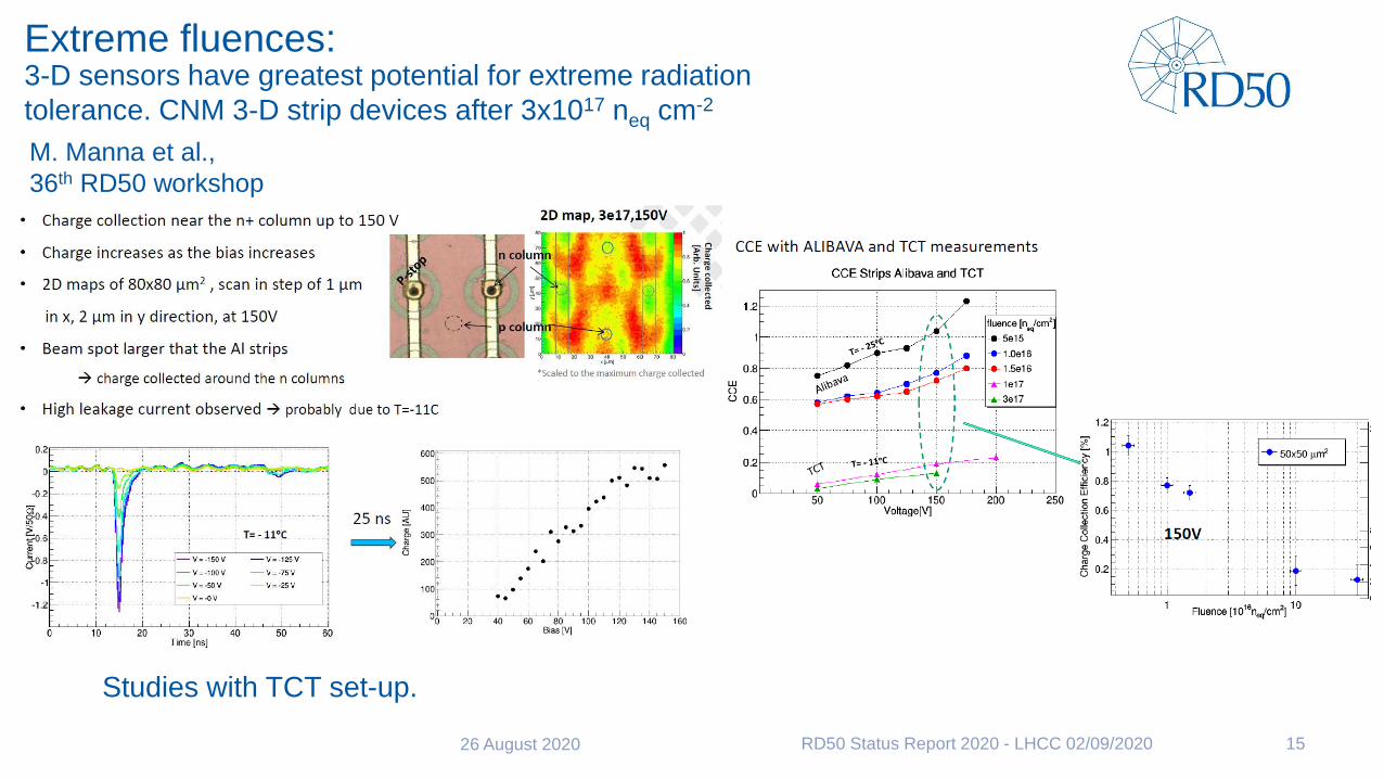
Extreme fluences:3-D sensors have greatest potential for extreme radiation
tolerance. CNM 3-D strip devices after 3x10¹⁷ neq cm-2
M. Manna et al.,
36th RD50 workshop
26 August 2020 RD50 Status Report 2020 - LHCC 02/09/2020
Studies with TCT set-up.

New Structures
Recent results 2019/20
26 August 2020 RD50 Status Report 2020 - LHCC 02/09/2020 16

Sensors for 4D tracking
LGAD: Low Gain Avalanche Detectors• Origin: Pioneered by RD50 with CNM, Barcelona (and later also FBK,Trento)
• RD50 working on LGADs since ≈2010 (> 50 production runs)
• Application: LGAD for timing detectors
• Intrinsic gain of devices allows for excellent timing performance (<50ps)
• Time-tagging of particle tracks in order to mitigate pile-up effects
• To be implemented in ETL (CMS) and HGTD (ATLAS)
• Concept: similar to APD but lower gain O(10), finely segmented for tracking
• Impact ionization in p+-implant (multiplication layer) produces gain
• Tailored multiplication layer ([B]~1017cm-3); challenge: optimize gain vs. breakdown
• Foundries:
• CNM (Barcelona, ES), FBK(Trento,IT), HPK (Japan), IHEP(Bijing, China), Micron(UK),
BNL(USA) and in preparation: CIS(Erfurt, Germany)
17
• Areas of LGAD developments within RD50
• Timing performance• Optimization: sensor thickness, gain layer profile and signal homogeneity (weighting field)
• Fill factor and signal homogeneity• Gain layer needs protection against breakdown (JTE) causing non-efficient area
• Mitigation: New and optimized LGAD concepts investigated
• Radiation Hardness • Problem: Field in gain layer dropping due to “acceptor removal”
• Defect Engineering of gain layer: Use Gallium instead of Boron or Carbon co-implant to impact on defect kinetics
• Modification of gain layer profile
• Performance Parameterisation Model• Predictive model for operation performance (radiation, temperature, thickness, annealing, ….)
26 August 2020 RD50 Status Report 2020 - LHCC 02/09/2020
𝜎𝑗𝑖𝑡𝑡𝑒𝑟2 =
𝑁𝑜𝑖𝑠𝑒
𝑑𝑉/𝑑𝑡≈𝑡𝑟𝑖𝑠𝑒𝑆/𝑁
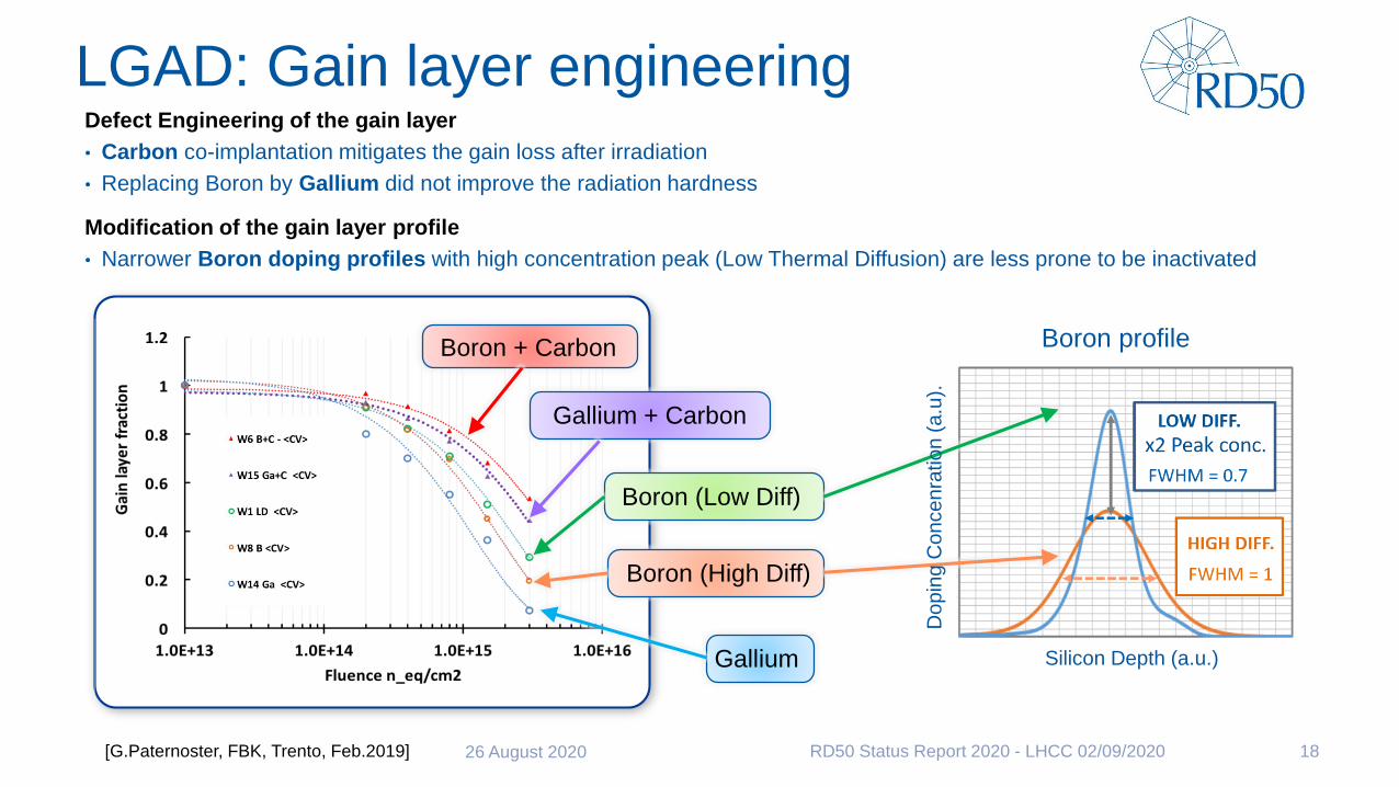
LGAD: Gain layer engineeringDefect Engineering of the gain layer
• Carbon co-implantation mitigates the gain loss after irradiation
• Replacing Boron by Gallium did not improve the radiation hardness
Modification of the gain layer profile
• Narrower Boron doping profiles with high concentration peak (Low Thermal Diffusion) are less prone to be inactivated
18
Boron + Carbon
Gallium + Carbon
Gallium
Boron (High Diff)
Boron (Low Diff)
Silicon Depth (a.u.)
Do
pin
g C
on
ce
nra
tio
n(a
.u).
Boron profile
[G.Paternoster, FBK, Trento, Feb.2019] 26 August 2020 RD50 Status Report 2020 - LHCC 02/09/2020

LGAD: Annealing after Irradiation• Annealing changes Neff with time after irradiation: check for influence on timing response.
• Important for temperature scenario in experiments!
• Experiment: HPK LGAD sensors (1.3 x 1.3 mm2), 50 mm thickness, neutron irradiated (4x10¹⁴ to 3 x 10¹⁵ neq/cm2), annealing at 60°C
19
Better charge collection and time resolution for 0 min annealing;
after that no strong change (with exception of very long annealing > 10.000 min)
26 August 2020 RD50 Status Report 2020 - LHCC 02/09/2020[G.Kramberger, JSI – 36th RD50 Workshop 6/2020]
Charge collection (beta source) time resolution
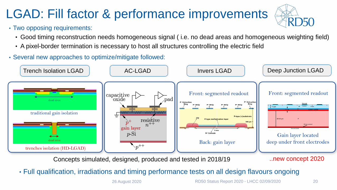
LGAD: Fill factor & performance improvements• Two opposing requirements:
• Good timing reconstruction needs homogeneous signal ( i.e. no dead areas and homogeneous weighting field)
• A pixel-border termination is necessary to host all structures controlling the electric field
• Several new approaches to optimize/mitigate followed:
26 August 2020 RD50 Status Report 2020 - LHCC 02/09/2020 20
Trench Isolation LGAD
• Full qualification, irradiations and timing performance tests on all design flavours ongoing
AC-LGAD Invers LGAD
traditional gain isolation
dead area
trenches isolation (HD-LGAD)
dead area
Front: segmented readout
Back: gain layer
Concepts simulated, designed, produced and tested in 2018/19
Deep Junction LGAD
..new concept 2020
Front: segmented readout
Gain layer located
deep under front electrodes

21
M. Tornago et al.,
36th RD50 workshop
LGAD design variation: resistive AC-
coupled Silicon Detectors
Designed for 4-D
tracking, 100% fill
factor.
26 August 2020 RD50 Status Report 2020 - LHCC 02/09/2020
Position
Timing

22
LGAD design variation: Deep Junction LGAD
Y. Zhao et al., 36th
RD50 workshop
Designed for high granularity and 100% fill factor.
26 August 2020 RD50 Status Report 2020 - LHCC 02/09/2020

RD50: CMOS developments (150 nm)
26 August 2020 RD50 Status Report 2020 - LHCC 02/09/2020 23
2017 2018 2019 2020
RD50-MPW1 RD50-DAQ (Caribou) Hit map e-TCT after irradiation
RD50-MPW1 I-V
RD50-MPW2
TCADI_LEAK
V_BD Improved
electronics
performance
2020/21
MPW3
[E.Viella Figueras, Liverpool - RD50 Workshop 6/2020]
Timeline: good results with MPW2, intense characterisation campaign, move design forward to frontier performance (speed, size, …)

24
HV-Cmos developments (150 nm)
E. Vilella et al., 36th
RD50 workshop
Timeline: good results with MPW2, intense characterisation campaign,
move design forward to frontier performance (speed, size, …)
One more MPW to
push performance
26 August 2020 RD50 Status Report 2020 - LHCC 02/09/2020

Full Detector Systems
Recent results 2019/20
26 August 2020 RD50 Status Report 2020 - LHCC 02/09/2020 25

Radiation Effects in LHC Experiments
• 5 workshops on “Radiation Effects at LHC Experiments and Impact on
Operation and Performance” organized (2011 - 2019)
• Common Workshop: (ALICE), ATLAS, CMS, LHCb, RD50
• Sensor Measurements
• Electronics/Optoelectronics
• Radiation Simulation and Monitoring
• Sensor Simulation
• Outcome and follow-up:
• Generally good agreement between RD50 damage prediction models
(e.g.“Hamburg model”) and radiation damage observed by the LHC
experiments.
• More coherent approach in data analyses agreed and documented.
• Modelling will have to be refined in some areas for run 3 !
• CERN Yellow Report written and edited by a team from RD50 & all
LHC experiments is under preparation (150 pages, in review phase)
summarizing observations, comparing results from different
experiments against each other, listing open questions and outlining
further work towards Run 3.
26 August 2020 RD50 Status Report 2020 - LHCC 02/09/2020 26

Radiation Effects in LHC Experiments
• Workshop on radiation effects in LHC Experiments (Feb.2019)
26 August 2020 RD50 Status Report 2020 - LHCC 02/09/2020 27
ATLAS B-layer
data vs. MC&NIEL
strong z-dependence;
unexpected
Plots: Radiation Effects Workshop Feb.2019K.Mochizuki(ATLAS SCT) J.L.Agram (CMS Tracker), Aiden Grummer
(ATLAS Pixel) , G.Sarpis (LHCb Velo) , F.Feindt (ATLAS Pixel)
Leakage currents in ATLAS SCT
and CMS tracker and model predictions
LHCb Velo depletion voltage
reduced by annealing;
according to model
CMS pixel layers;
deviation of Vdep from
modelling at high fluences

28
In collaboration with experiments: monitoring radiation
B. Nachman et al., 36th RD50 workshop 26 August 2020 RD50 Status Report 2020 - LHCC 02/09/2020

Spare slides
26 August 2020 RD50 Status Report 2020 - LHCC 02/09/2020 29

RD50 Work Plan
26 August 2020 RD50 Status Report 2020 - LHCC 02/09/2020 30

RD50 – 5 Year Work Plan• 5 year work program submitted in May 2018
• Approved by CERN Research Board in June 2018
• Workplan [70 milestones]
• Defect and Material Characterization [16 MS]
• p-type silicon [7 MS]
• Cluster defects [4 MS]
• Theory of defects [5 MS]
• Device Characterization & Device Simulation [21MS]
• Silicon materials [5 MS]
• Extreme fluences [5 MS]
• Experimental techniques [3 MS]
• Surface damage [1 MS]
• TCAD simulations [7 MS]
• New structures [21 MS]
• 3D sensors [6 MS] ; LGAD [4 MS]
• CMOS [6 MS] ; New Materials [5 MS]
• Full Detector Systems [12 MS]
• LHC [7 MS]; HL-LHC [3 MS]
• FCC [2 MS]
26 August 2020 RD50 Status Report 2020 - LHCC 02/09/2020 31
https://cds.cern.ch/record/2320882/files/LHCC-SR-007.pdf

WP1: Defect and Material
Characterization
• Main activities• Detection and microscopic characterization of standard and material engineered silicon via dedicated
techniques (DLTS, TSC, TDRC, SIMS, ICP-MS, PITS, FTIR, TCT, EPR, HRTEM)
• Identification of electrically active defects induced by irradiation responsible for trapping, leakage current,
change of Neff , change of E-Field
• Studying possible application for radiation hardening
• Deliver input for device simulations (e.g. TCAD) to predict detector performance under various conditions
• 16 Milestones [2018-2022]
• WP 1.1 p-type silicon [7 MS]
• WP 1.2 Cluster defects [4 MS]
• WP 1.3 Theory of defects and defect kinetics modeling [5 MS]
26 August 2020 RD50 Status Report 2020 - LHCC 02/09/2020 32

Defect and Material
Characterization• WP 1.1. Electrically active defects in p-type silicon
Analysis of electrically active defects and of the radiation induced changes in the electrical
characteristics of devices built on p-type silicon.
• M1: Detection and characterization of all radiation induced defects in STFZ and engineered silicon (Q3/2019)
• M2: Determine defect annealing behaviour in STFZ and engineered silicon. Correlation with device
performances (Q4/2019) [M1/M2: some ongoing work on epi sensors]
• M3: Determine defect transformations and kinetics in STFZ and engineered silicon after treatments at high
temperatures (between 150 °C and 350 °C). Correlation with the device performance (Q3/2020)
• M4: Identify the role of impurities in defect formation (Q1/2021)
• M5: Detection/characterization of radiation induced defects in LGAD and HV-CMOS sensors made with
STFZ and engineered p-type silicon, establishing annealing behaviour and correlation with electrical
performance (Q3/2021)
• M6: Validity tests on optimized material engineered sensors (pads, LGADs and HV-CMOSs). Comparison
between prediction and experiments (Q1/2022)
• M7: Validity tests on finally optimized material engineered sensors (pads, LGADs and HV-CMOSs) (Q3/2023)
26 August 2020 RD50 Status Report 2020 - LHCC 02/09/2020 33
2019
Milestones
2021
milestonesChallenge!
MS colour coding:
• fully achieved
• ongoing/ mostly achieved
• to be done / partly achieved
2020 Milestone
2022/23
milestones

Defect and Material
Characterization
• WP 1.2. Microstructural Investigations on extended and clustered defectsThis work targets microstructural investigations of extended and clustered defects by electron microscopy:
• M1: Microstructural characterization of the radiation induced clustered defects (fluences between 1015 and 1017 neq cm-2) and monitoring of the evolution of clusters at 80 °C (Q3/2019)
• M2: In situ- annealing studies at 5 temperatures (between 150 °C and 350 °C) in order to determine the structural transformations of the extended and clustered defects (Q3/2020)
• M3: Microstructural characterization of the oxide-semiconductor interface in irradiated LGADs and HV-CMOS devices, time evolution at 80 °C (Q3/2021)
• M4: Microstructural characterization of the oxide-semiconductor interface in irradiated optimized LGADs and HV-CMOS devices (Q3/2022)
• WP 1.3 Theory of defects and defect kinetics modelling• M1: Modelling of the detected defect generation/kinetics and of the impact on the device performance corresponding to
annealing treatments at 80 °C (Q3/2020)
• M2: Modelling of the detected defect generation/kinetics and of the impact on the device performance corresponding to annealing at temperatures between 150 °C and 350 °C and final assessment of the role of the intentional added impurities (Q1/2021)
• M3: Identification of the optimal impurity concentrations for pads, LGADs and HV-CMOSs as input for production. (Q3/2021)
• M4: Improvements of the developed models according to validity test foreseen as 1.1-M6 and provide new optimization solutions for 5.1.1-M7. (Q3/2022)
• M5: Validity test for the developed theoretical models based on the results obtained on 1.1-M7 optimized sensors (Q3/2023)
26 August 2020 RD50 Status Report 2020 - LHCC 02/09/2020 34
MS colour coding:
• fully achieved
• ongoing/ mostly achieved
• to be done / partly achieved

WP2: Device Characterization
and Device Simulation
• 21 Milestones [2018-2022]
• WP 2.1. Silicon materials [5 MS]
• WP 2.2. Extreme fluences [5 MS]
• WP 2.3. Experimental techniques [3 MS]
• WP 2.4. Surface damage [1 MS]
• WP 2.5. TCAD simulations [7 MS]
26 August 2020 RD50 Status Report 2020 - LHCC 02/09/2020 35

WP 2: Device Characterization
and Device Simulation
• WP 2.1. Silicon Materials
FZ p-type silicon will be used for ATLAS and CMS upgrades. In running pixel systems
oxygen enriched (DOFZ) n-type with n-side readout is used. For radiation hardening
different impurity engineered material like MCz, oxygen enriched epitaxial (DOEPI) or
nitrogen enriched FZ or EPI will be tested. Also the optimal thickness of the sensor
material has to be studied in more detail.
• M1: Development of impurity engineered p-type silicon with possible vendors (Topsil for N
enriched FZ, …) (Q3/2019)
• M2: Search for possible production of nitrogen enriched epitaxial silicon (e.g. ITME) (Q3/2019)
• M3: Production of diodes, strip and pixel sensors with engineered materials by different vendors
(CiS, CNM, FBK, ….) and field tests (Q3/2019)
• M4: Several irradiation campaigns with different particles up to fluences exceeding 1017 neq/cm2
on standard and engineered materials (Q4/2020)
• M5: Macroscopic studies on all irradiated devices including Edge-TCT, TPA-TCT and
investigations with radioactive sources/test-beams, including annealing studies (Q3/2023).
26 August 2020 RD50 Status Report 2020 - LHCC 02/09/2020 36

WP2: Device Characterization
and Device Simulation
•WP 2.2. Extreme Fluences
Device properties (I-V, C-V-f, CCE) on different p-type silicon materials to
fluences ranging from 1016 to 5×10¹⁷ neq cm-2 with neutrons and protons of
different energies.
• M1: Precise mobility parametrization for electrons and holes (Q4/2019)
• sum of hole and electron mobility characterized (effective mobility)
• M2: Development of method for extraction of trapping times/distances from the
measured data (Q3/2020)
• M3: Establishing leakage current behavior at extreme fluences (Q3/2020)
• M4: Measurement of recombination lifetimes in silicon bulk (Q3/2021)
• M5: Modeling/parameterization of CCE(fluence, voltage, annealing time)
(Q3/2023)
26 August 2020 RD50 Status Report 2020 - LHCC 02/09/2020 37

WP2: Device Characterization
and Device Simulation
• WP 2.3. Experimental techniquesBeside standard device characterization tools (I-V, C-V, TCT), more complex systems like “Edge-TCT” and
“Two Photon Absorption (TPA)” technique became available.
• M1: Full specification of a TPA-TCT method for the characterization of irradiated devices (Q4/2018)
• M2: Commissioning of the top-bench fiber-based femto second laser TPA-TCT setup at the SSD/CERN (Q4/2019).
• M3: Phenomenological parametrization of the radiation effects on diodes using the TPA-TCT method (Q3/2020)
• WP 2.4. Surface Damage
The build-up of oxide charges in the passivation layers and traps in the SiO2-Si interface by ionizing
radiation influences the electric field at the structured implants and the surface generation current. This
affects the performance of irradiated sensors and it can be of increasing importance with thin and more
complex devices (e.g. HV-CMOS). RD50 has a dedicated research effort.
• M1:Investigation of surface damage on test structures with oxide and oxide-nitride passivation layers
irradiated with protons up to 1MGy (Q3/2020).
• no focus in this area at the moment; existing parameterizations are sufficient for modeling
26 August 2020 RD50 Status Report 2020 - LHCC 02/09/2020 38

WP2: Device Characterization
and Device Simulation
• WP 2.5. TCAD simulations and custom device simulators
• M1: Comparison of commercial TCAD tools; preparation of a recommendation for
parameters and physics models (Q4/2019)
• …document in preparation (Status presented on 06/2020 RD50 Workshop)
• M2: Development of a reliable radiation damage model (I-V, C-V, CCE and the E-
field) covering the HL-LHC fluences for protons and neutrons for a given operation
temperature (Q4/2020)
• M3: Model M1 extended to cover temperature dependence of the bulk-damage
related effects from room temperature down to -30 °C. (Q3/2021):
• M4: Model from M2 extended to cover annealing effects (Q3/2022):
• M5: Model of the donor and acceptor removal (SiPMs, LGAD, CMOS,..) (Q3/2020):
• M6: Surface damage model with implementation of surface damage in p-type
segmented sensors (Q1/2021)
• M7: Evaluation of possible implementation of cluster defects in commercial TCAD
device simulators using a charge carrier occupation dependent energy level
distribution (Q2/2021)
26 August 2020 RD50 Status Report 2020 - LHCC 02/09/2020 39

WP3: New Structures
New structures based on silicon substrates are, possibly together with
materials other than silicon, the most promising options to extend
radiation tolerance to the region of 7-8×10¹⁷ neq/cm2.
• 21 Milestones [2018-2022]
• WP3.1 3D sensors [6 MS]
• WP 3.2 LGAD [4 MS]
• WP 3.3 CMOS [6 MS]
• WP 3.4 New Materials [5 MS]
26 August 2020 RD50 Status Report 2020 - LHCC 02/09/2020 40

WP3.1: 3D detectors
• WP 3.1. 3D detectors
• M1: full radiation tolerance study of 3D pixels connected to the RD53A chip (Q3/2019).
• M2: radiation tolerance studies of 25x100-1E pixel cell design and the feasibility (yield) of
the 25x100-2E pixel cell layout (Q4/2019).
• M3: final radiation tolerance study of 3D pixels connected to the RD53B chip (Q4/2020)
• M4: Understanding the limit of the radiation hardness of the 3D geometry up to 1017neq/cm2
(Q2/2021)
• M5: Evaluation of the time performances of new 3D geometries (Q3/2020).
• M6: Design and simulation of new 3D detectors geometries for operation at 8x10¹⁷neq/cm2
(Q4/2022).
26 August 2020 RD50 Status Report 2020 - LHCC 02/09/2020 41
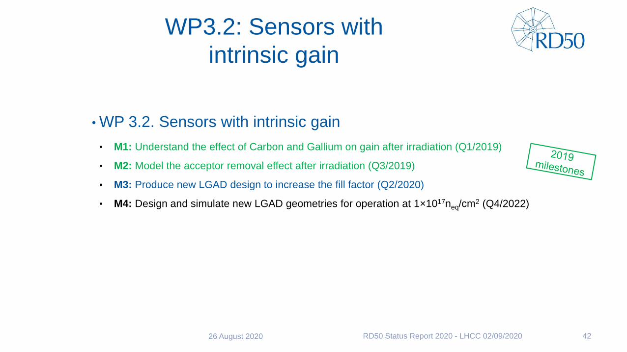
WP3.2: Sensors with
intrinsic gain
• WP 3.2. Sensors with intrinsic gain
• M1: Understand the effect of Carbon and Gallium on gain after irradiation (Q1/2019)
• M2: Model the acceptor removal effect after irradiation (Q3/2019)
• M3: Produce new LGAD design to increase the fill factor (Q2/2020)
• M4: Design and simulate new LGAD geometries for operation at 1×10¹⁷neq/cm2 (Q4/2022)
26 August 2020 RD50 Status Report 2020 - LHCC 02/09/2020 42

WP3.3: CMOS
and monolithic devices
• WP 3.3. CMOS and monolithic devices
• M1: Characterization of the diodes and readout electronics of unirradiated and irradiated RD50-MPW1 samples (Q4/2018).
• New intermediate milestone M1.2: Design and submission of RD50-MPW2 (Q1/2019). Achieved
• New intermediate milestone M1.3: Characterization of unirradiated and irradiated RD50-MPW2 samples (Q4/2019, Q1/2020).
Developing DAQ at the moment
• M2: Design and submission for fabrication of RD50-ENGRUN1 (Q4/2018). Ongoing
• M3: Characterization of unirradiated and irradiated RD50-ENGRUN1 samples (Q3/2019, Q3/2020).
Postponed
• M4: Characterization of irradiated backside biased RD50-ENGRUN1 samples for operation beyond 1016 neq/cm2 (Q4/2020).
Postponed
• M5: Studies of stitching process options (Q4/2021).
• M6: Characterization of unirradiated and irradiated stitched samples (Q4/2022).
26 August 2020 RD50 Status Report 2020 - LHCC 02/09/2020 43
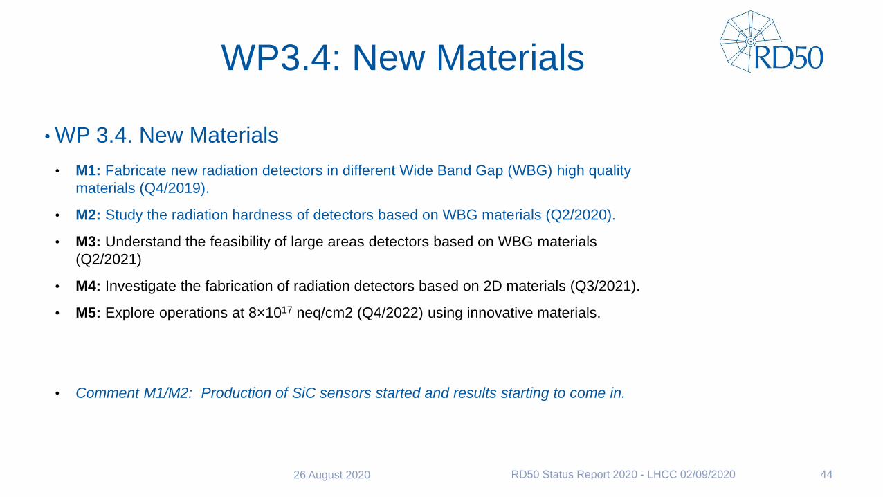
WP3.4: New Materials
• WP 3.4. New Materials
• M1: Fabricate new radiation detectors in different Wide Band Gap (WBG) high quality
materials (Q4/2019).
• M2: Study the radiation hardness of detectors based on WBG materials (Q2/2020).
• M3: Understand the feasibility of large areas detectors based on WBG materials
(Q2/2021)
• M4: Investigate the fabrication of radiation detectors based on 2D materials (Q3/2021).
• M5: Explore operations at 8×10¹⁷ neq/cm2 (Q4/2022) using innovative materials.
• Comment M1/M2: Production of SiC sensors started and results starting to come in.
26 August 2020 RD50 Status Report 2020 - LHCC 02/09/2020 44

WP4: Full Detector SystemsExtensive studies of segmented detectors are being performed withinRD50 with strip and pixel readout systems especially developed byAlibava and PSI. RD50 is an ideal testing environment for thedevelopment of detection systems. RD50 methods are complementaryto the ones of the large experiments and are based on mini-stripdetectors and pixels. Beyond the measurements on the segmentedsensors, RD50 contributes to the analyses and understanding of datataken on the operating experiments.
• 12 Milestones [2018-2022]
• WP 4.1 LHC [7 MS]
• WP 4.2 HL-LHC [3 MS]
• WP 4.3 FCC [2 MS]
26 August 2020 RD50 Status Report 2020 - LHCC 02/09/2020 45

Full Detector Systems
• WP 4.1. LHC: Radiation Damage in operating
tracking detectorsRD50 has a unique role in creating tools and dialogue for the modelling and monitoring of
in-situ detector systems and actively collaborates with ATLAS, CMS, and LHCb.
• M1: Hold a follow-up radiation damage workshop at the end of Run 2. Produce CERN Yellow Report
documenting the status and experience gathered (Q1/2019).
• M2: Develop common software that can be used for making comparisons to irradiated sensors at test
beams (Q3/2019).
• M3: Complete a program of irradiation and test beam campaigns with accurate thermal control to
carefully study the impact of annealing with Run 2-like levels of irradiation (Q3/2019).
• M4: Using the full Run 2 dataset and digitization models that incorporate radiation damage, tune TCAD
radiation damage parameters to data and establish systematic uncertainties on these parameters.
RD50 will maintain a database of models and parameters (Q4/2019).
• M5: Using the full Run 2 dataset, lab and test beam data to develop a model that incorporates a non-
uniform E-field and annealing effects (Hamburg + TCAD). The fine-tuning of this model will require
further work (Q4/2020).
• M 2021-2023: Repeat and extend the in-situ studies for Run 3.
• M6: During LS3 we intent to perform a post-operation characterization of de-installed LHC sensors.
RD50 Status Report 2020 - LHCC 02/09/2020 -46-26 August 2020

Full Detector Systems
• WP 4.2. HL-LHC• M1: Understanding dependence of CCE/CM in segmented detectors on long-term bias at different
annealing stages (Q4/2020).
• M2: Understanding the noise performance in CM operation mode at high voltages and modelling it for
fast electronics readout (Q4/2020).
• M3: Comparative studies of mini-strip detectors from two main producers (Infineon, HPK) in terms of
CCE/CM differences (Q4/2020). (Infineon no longer producing detectors)
• WP 4.3. FCC• M1: Punch Through Protection (PTP) structure at high fluences, beyond that of strip sensors (Q2/2021)
• M2: CCE studies of different geometry sensors after extreme fluences of up to 5-6×1017 cm-2 (3D
samples of different columns widths, mini-strips, pads). The most challenging action will be the readout
of segmented devices (Q3/2022).
RD50 Status Report 2020 - LHCC 02/09/2020 -47-26 August 2020

RD50 common projects• Common Projects (2017 – 2020)
• 2017-01 LGAD based on EPI wafers (G.Pellegini, CNM, Barcelona)
• 2017-02 TPA TCT on CMOS sensors (I.Vila, Santander)
• 2017-03 LGAD fabricated with epitaxial layer (G.Pellegrini, CNM, Barcelona)
• 2017-04 RD50 CMOS submission (Gianluigi Casse, Liverpool, UK / Vitaliy Fadeyev, SCIPP, USA)
• 2017-05 50 µm thin LGAD fabricated with Ga multiplication layer (Joern Lange, IFAE Barcelona)
• 2017-06 Thin LGADs characterization using IBIC and time-resolved IBIC at CAN (Carmen Jiménez-Ramos, Sevilla)
• 2017-07 MPW run with LFoundry (Eva Vilella, Liverpool)
• 2017-08 50 µm thin AC-LGAD (Mar Carulla, CNM Barcelona)
• 2018-01 Development of Segmented LGAD with small pixels and high Fill-Factor (Giovanni Paternoster, FBK)
• 2019-01 RD50-MPW2 (Eva Vilella, Liverpool)
• 2019-02 Proof of concept of 3D detectors fabricated in Silicon Carbide (SiC) semiconductor layers(Sofia Otero-Ugobono, CNM Barcelona)
• 2019-03 Schottky diodes on Epitaxial Silicon for Radiation Damage Characterization of CMOSMAPS (Giulio Villani, STFC Rutherford Appleton Laboratory)
• 2020-01: 3D detectors optimized for timing applications (Gregor Kramberger, JSI,Ljubljana)
• 2020-02: Proof-of-concept and radiation tolerance assessment of thin pixelated Inverse Low Gain Avalanche Detectors (ILGAD) (Ivan Vila, UC-CSIC, Santander)
26 August 2020 RD50 Status Report 2020 - LHCC 02/09/2020 48

Outlook & Request to LHCC• RD50 outlook:
• Roadmap given in 5 Year Workplan (2018-2023) https://cds.cern.ch/record/2320882
• Milestone status discussed in depth with LHCC referee on 26.8.2020 (i.e. today)
• RD50 MOU
• RD50 Memorandum of Understanding (MoU) finalized and signed by CERN Research DG in May 2019
• Resources:
• Every RD50 institution is contributing 2kCHF/year to the RD50 common fund (CF).
• The CF is used to finance common projects and to support common activities.
• "RD50 common projects" receive a financial contribution from the CF within rules defined in the MOU.
Remaining costs are shared between the institutions participating in the project.
• Most RD50 projects are performed as in-kind contributions supported by other funding (national funding
agencies, successful competitive funding proposals,….).
• RD50 is planning to continue this funding concept.
• Resources from CERN (Host lab) (as previous years)
• Operation of the RD50/Solid State Detectors Lab (1 physicist, 0.5 technician & 100kCHF/year)
• Access to CERN and EP-DT facilities: Irradiation facilities, Bond Lab, Solid State Detector Lab,…
• Administrative support at CERN through EP-DT secretariat
• Acknowledgement:
• The CERN RD50 core team is supported through the EP Department and participates in the CERN EP
R&D program for future experiments.
26 August 2020 RD50 Status Report 2020 - LHCC 02/09/2020 49