continuous-flow bioseparation using microfabricated
TRANSCRIPT
nature protocols | VOL.4 NO.11 | 2009 | 1681
p
uor
G g
n ih si l
bu
P eru ta
N 900 2©
nat
ure
pro
toco
ls/
moc. e r
ut an .
ww
w / /:pt t
h
protocol
IntroDuctIonCompared with the conventional bioanalysis and diagnostic meth-ods, direct analysis of biologically relevant molecules (e.g., proteins and nucleic acids) can potentially enhance speed, accuracy and sen-sitivity1,2. Moreover, direct biomolecule observations and manip-ulations help investigators to probe the fundamental molecular processes in biochemistry and biophysics that are often obscured in ensemble assays3–5. Therefore, nanofluidic systems with character-istic dimensions comparable with molecular scale can provide new opportunities for direct observation, manipulation and analysis of biomolecules, and these nanofluidic systems can potentially provide innovative platforms to achieve ultrasensitive and high-resolution biosensing and detection6,7. Inspired by this concept, over the past 10 years, there has been a surge of research effort from different scientific disciplines to design and fabricate different nanofluidic systems (with characteristic size scales between 10 to 100 nm) for biological and biomedical applications6,7. Among this surge, one notable research thrust is to design efficient and regular artificial molecular sieving structures that can be a potential alternative to the conventional gel-based separation methods to improve the speed and resolution of biomolecule separation8–10.
The development of efficient nanofluidic sieving structures is essential for optimizing biomolecule separation methods in a chip format within a complete microanalysis environment8–11. These nanofluidic structures can provide flexible designs and offer pre-cise control over the constraining geometries ideal for molecular sieving and separation. Moreover, the current research thrust in microfluidic based scaled-down analytical processes is stimulat-ing development of different chip-based methods, where bioanaly-sis can be carried out in a faster and lower cost manner7,12,13. The random nanoporous gel materials that are conventionally used in routine bioseparation applications unfortunately have intrinsic difficulties being integrated into automated multistep chip-based bioanalysis systems. Therefore, the development of a versatile
regular nanofluidic-sieving structure that can monolithographi-cally be integrated within highly complex bioanalysis microsystems will have profound implications for different biological and biomedical applications.
Over the past decade, there have been exciting developments in the field of artificial regular sieving structures due to the advancements of microtechnology and nanotechnology8–10. So far, a myriad of regular sieve designs have been demonstrated with varying degrees of success in biomolecule separation14–18. These reported artificial sieving structures have primarily been success-ful for the separation of large biomolecules, such as viral DNA (as reviewed in ref. 10). Recently, we have introduced a unique regular molecular sieving structure called the anisotropic nanofluidic-filter (nanofilter) array (ANA)19,20 and have demonstrated its implemen-tation for high-resolution continuous-flow separation of a wide range of DNA fragments (between 50 to 23,000 bp) and proteins (between 11 to 400 kDa) within a few minutes. In this protocol we describe the detailed fabrication of the ANA chips and how to perform continuous-flow bioseparation using these chips.
Comparison with gel-based separation methodsCurrently, the separation of biomolecules in a biology laboratory is routinely achieved with gel-based separation techniques, such as gel-exclusion chromatography and slab-gel electrophoresis21,22. These gel-based separation techniques use gelatinous materials that consist of cross-linked three-dimensional nanometer-sized pore networks. Despite the popularity of both the gel-based separation methods, they still exhibit several limitations that make neither method optimal in separating complex mixtures for downstream analysis21. For example, the chief limitations of gel-exclusion chromatography are that the separation can be slow and that the resolution of the emerging peaks is limited, and in addition, rela-tively large amounts of samples are necessary to obtain visible and
Continuous-flow bioseparation using microfabricated anisotropic nanofluidic sieving structuresJianping Fu1, 2, 4, Pan Mao3 & Jongyoon Han2
1Research Laboratories of Electronics, Massachusetts Institute of Technology, Cambridge, Massachusetts, USA. 2Department of Electrical Engineering and Computer Science, Department of Biological Engineering, Massachusetts Institute of Technology, Cambridge, Massachusetts, USA. 3Department of Mechanical Engineering, Massachusetts Institute of Technology, Cambridge, Massachusetts, USA. 4Current address: Department of Mechanical Engineering, University of Michigan, Ann Arbor, Michigan, USA. Correspondence should be addressed to J.F. ([email protected]).
Published online 29 October 2009; doi:10.1038/nprot.2009.176
the anisotropic nanofluidic-filter (nanofilter) array (ana) is a unique molecular-sieving structure for separating biomolecules. In this protocol we describe the fabrication of planar and vertical ana chips and how to perform continuous-flow bioseparation using them. this protocol is most useful for bioengineers who are interested in developing automated multistep chip-based bioanalysis systems and assumes previous cleanroom microfabrication knowledge. the ana consists of a two-dimensional periodic nanofilter array, and the designed structural anisotropy of ana causes different-sized or charged biomolecules to follow distinct trajectories under applied electric fields, leading to efficient continuous-flow separation. using microfluidic channels surrounding the ana, the fractionated biomolecule streams are collected and routed to different fluid channels or reservoirs for convenient sample recovery and downstream bioanalysis. the ana is physically robust and can be reused repeatedly. compared with the conventional gel-based separation techniques, ana offers the potential for faster separation, higher throughput and more convenient sample recovery.

1682 | VOL.4 NO.11 | 2009 | nature protocols
p
uor
G g
n ih si l
bu
P eru ta
N 900 2©
nat
ure
pro
toco
ls/
moc. e r
ut an .
ww
w / /:pt t
h
protocol
well-resolved bands. In slab-gel electrophoresis, recovery of the separated sample is often problematic and inefficient; the location of the band in the gel must be physically cut out, and additional washing steps are necessary to extract the desired sample from the gel, which often lead to significant sample loss21.
Recently, gel-based sieving structures have successfully been incorporated into different chip-based bioanalysis systems to separate both nucleic acids and proteins23,24. These gel-based microsystems have provided convincing evidences for separa-tion speed and resolution. However, as mentioned earlier, these gel-based microsystems still pose the intrinsic difficulties for inte-gration with other bioanalysis components and packaging as a whole lab-on-chip system. Most of these gel-based microanalysis systems are not reusable, economically not an ideal choice for large-scale screen for different systems-biology applications. In contrast, the ANA can monolithographically be integrated within bioanalysis microsystems, as an upstream sample preparation component to separate and purify complex biological samples, and the ANA is physically robust and can be reused repeatedly19,20.
Compared with the gel-based sieving structures, two major limitations currently exist for the ANA: separation resolution and sample throughput. The ANA structure needs to be further optimized for separation resolution to fully realize its promise for on-chip based proteomic research and biomarker discovery. The current size selectivity of the ANA structure is about 2–3 nm, which corresponds to the end-to-end distance of 10-bp DNA; how-ever, it is still not optimal for protein separation. In the future, an improved ANA structure should have size selectivity comparable to the gel-based techniques and should discriminate and separate proteins (either native or denatured) with a molecular weight difference of about 5 kDa. Two approaches might be undertaken to further improve size selectivity, and therefore separation resolution of the ANA structure. First, the size selectivity of the ANA should be improved by scaling down the nanofilter structures (period, gap size, etc.) with advanced sub-100-nm resolution lithography tech-niques25,26. We have proved both theoretically and experimentally that the size selectivity of ANA is inversely proportional to both the nanofilter period (pitch size) and the nanofilter gap size27,28. Second, it is possible to extend the separation functionality of the ANA structure by utilizing the Debye layer, electro-osmosis and surface chemistries, together with the geometrical constraints of the ANA, to achieve biomolecule separation based on a suite of molecular properties (e.g. size, charge or hydrophobicity)10. For example, we have recently demonstrated that by actively controlling the buffer ionic strength and therefore the Debye length, switch-able size- or charge-based separation of proteins can be achieved within the ANA19.
The sample throughput of the ANA also needs to be improved for its future implementations in different biological and biomedi-cal applications, even though this concern is alleviated greatly by the ever increasing number of on-chip biosensing and detection mechanisms and their much improved detection limits. For the current ANA design, the maximum volume throughputs for protein samples are in the range of µl h − 1. In the future, large-scale bioseparations in a chip format with high sample through-put (in the range of µl min − 1) would be desired. A key for this functional goal would be to devise a convenient and inexpensive method to fabricate robust molecular sieves with highly parallel nanopores.
Comparison with other micro/nanofluidic sieving structuresRecently, different regular micro/nanofluidic sieving structures have been reported in the literature to separate biomolecules, such as viral DNA, with fast speed and great resolution14–18. One notable example was the ‘DNA Prism’ devised by Huang et al.15 to continu-ously separate long DNA fragments (61–209 kbp) within a few minutes, a speed much faster than conventional pulsed-field gel electrophoresis (PFGE) and pulsed-field capillary electrophoresis. Han and Craighead14 have recently designed an entropy trap array device to separate long DNA ladder samples (5–50 kbp) in about 30 min. The ANA structure described in this protocol is a more recent development, and it offers several distinct advantages when compared with these previously reported micro/nanofluidic sieving structures, rendering it a promising generic molecular sieving struc-ture for an integrated bioanalysis microsystem29–31. These unique advantages of the ANA include the following: (a) the capability to continuously separate physiologically relevant molecules including proteins in a few minutes; (b) the versatile separation mechanisms (e.g., Ogston sieving, entropic trapping and electrostatic sieving) that can take effect in the ANA to separate biomolecules cover-ing broad biological size ranges and based on different molecular properties; (c) the continuous-flow operation of the ANA that facilitates the integration of the separation step with upstream or downstream analysis steps; thus, allowing the bioseparation to be performed ‘in-line’ with other continuous flow processes; (d) the continuous-flow operation of the ANA allows downstream sam-pling (either of a detection signal or of the separated biomolecules themselves) to be time-integrated to improve the detection limit. In our opinion, these advantages of the ANA can have profound implications for proteomic research and biomarker discovery on a chip format32,33.
This protocol is most useful for bioengineers and bioanalytical chemists who are interested in developing automated multistep chip-based bioanalysis systems7,12,13. As the fabrication process of the ANA structure involves standard microfabrication techniques in a cleanroom environment, the researchers implementing this protocol need to receive necessary training from the cleanroom staffs about how to operate the required cleanroom equipments. Ideally, the researchers should either assume previous knowledge and experience in cleanroom microfabrication or have direct input of a cleanroom technologist in the research team. It is our goal that with the guidance of this protocol, the ANA structures can be fabricated in a fully equipped and well-staffed cleanroom. It is also worth mentioning that, now that many different well-equipped microfabrication foundries are available worldwide for fabricating micro/nanoscale devices, even if the necessary microfabrication facility is not available locally or on campus, the designs of the ANA structure can still be outsourced to fabrication foundries.
In this protocol, the design and fabrication methods for two different types of the ANA—the planar ANA19 (Fig. 1a, as discussed in PROCEDURE) and the vertical ANA20 (Fig. 1b, as discussed in the Box 1)—will be discussed in detail. The design of both the ANA structures consists of a two-dimensional periodic nanofilter array, and the designed structural anisotropy of the ANA causes different-sized or charged biomolecules to follow distinct trajectories, leading to efficient continuous-flow separation. The ANA structures are batch fabricated using conventional semi-conductor microfabrication techniques on a silicon wafer. Using standard microfabrication techniques, such as photolithography,

nature protocols | VOL.4 NO.11 | 2009 | 1683
p
uor
G g
n ih si l
bu
P eru ta
N 900 2©
nat
ure
pro
toco
ls/
moc. e r
ut an .
ww
w / /:pt t
h
protocol
reactive ion etching (RIE) or deep reactive ion etching (DRIE) and anisotropic potassium hydroxide (KOH) etching, the ANA structures with a nanofilter gap size down to about 10 nm can be fabricated27,34. Three different separation mechanisms have been demonstrated successfully with the ANA to separate both DNA and proteins based on either size (Ogston sieving or entropic trapping) or charge (electrostatic sieving)19. In the planar ANA structure, the
relevant nanoscale constriction dimension of the planar nanofilter is etched by the RIE technique into the thickness direction of the silicon substrate (Fig. 1a); whereas in the vertical ANA, the nano-scale constriction of the vertical nanofilter is fabricated by taking advantage of the highly selective anisotropic KOH wet etching of the (110) silicon planes for high-aspect-ratio silicon structures with smooth and vertical sidewalls (Fig. 1b).
In the Experimental Design, we first discuss the different separation mechanisms applicable for the ANA to separate bio-molecules covering different size ranges and based on different molecular properties, and then we describe in detail the design guidelines of the ANA structure and the different microfabrication techniques involved in the ANA fabrication. Finally we describe the implementations of the ANA to separate different bio-molecules such as DNA and proteins. In the PROCEDURE, a step- by-step description of the fabrication process is provided, followed by a troubleshooting table with information on how to trouble-shoot the most likely problems encountered with the protocol. In the ANTICIPATED RESULTS, we briefly describe the likely outcome of using the ANA to separate biomolecules for different applications.
Experimental designSieving mechanisms in ANA. Three different separation mecha-nisms (i.e., Ogston sieving, entropic trapping and electrostatic sieving) have been applied in the ANA to separate biomolecules covering different size ranges and based on different molecular properties (see ref. 10 for a detailed discussion of these separa-tion mechanisms). For both Ogston sieving and entropic trapping, bioseparation should be conducted at high-ionic strength, wherein the Debye length becomes negligible compared with the nanofilter constriction size. Ogston sieving is effective for biomolecules with diameters smaller than the nanofilter constriction. Smaller molecules have a higher tendency to jump across the nanofilter and therefore assume a larger stream deflection angle in the ANA. In entropic trapping, diameters of biomolecules are greater than the nanofilter constriction size, and passage requires the molecules to deform to sneak through the nanofilter constriction. As longer molecules have a greater probability to jump across the nanofilter constriction, they will assume a greater deflection angle in the ANA. For low-ionic strength solutions, wherein the Debye length becomes comparable to the nanofilter constriction size, electro-static interactions (either repulsive or attractive) between charged biomolecules and charged nanofilter walls become prominent and start to dictate jump dynamics across the nanofilter. Therefore, similar-sized biomolecules bearing different net charges are energetically favored to different degrees for passage through the nanofilter, resulting in efficient separation in the ANA. In practice, Ogston sieving and entropic trapping are most suitable for size separation of linear flexible biomolecules such as DNA and dena-tured proteins, whereas electrostatic sieving is most suitable for separation of native biomolecules, such as globular proteins, by both size and charge19. In addition, electrostatic sieving under the low-ionic strength buffer can result in markedly increased size selectivity, and therefore higher separation resolution for nega-tively charged biomolecules in the ANA35. This enhancement in size selectivity is likely because of an effective decrease in the nanofilter constriction size due to electrostatic repulsion between negatively charged biomolecules and like-charged nanofilter walls.
a Planar ANA device
Si wafer
ANA shallow region
ANA deep region
(i) RIE to pattern theANA shallow regions
(ii) RIE to pattern theANA deep regions
(iii) Thermal oxidation toprovide electrical isolation
(iv) Anodic bonding toform sealed ANA device
Thermal oxide
b Vertical ANA device
(i) KOH etching to pattern theANA narrow regions
(ii) DRIE to pattern theANA wide regions
(iii) Thermal oxidation toprovide electrical isolation
(iv) PECVD deposited oxide toform sealed ANA device
ANA narrow region
ANA wide region
Thermal oxide
PECVD oxideGlass
Planar nanofilter Vertical nanofilter
Figure 1 | Schematic of the fabrication process for both the planar and vertical ANA devices. In brief, for the planar ANA device (a), the shallow and deep regions of the ANA are defined and etched into a Si wafer using photolithography and RIE. KOH etching is performed to etch through the wafer for creating buffer access holes (not shown). A thick thermal oxide layer is grown to provide an electrical isolation between the conductive Si substrate and buffer solution. Finally, the ANA device is sealed by bonding a Pyrex wafer on the front surface of the silicon wafer. For the vertical ANA device (b), the narrow and wide regions of the ANA are defined and etched into a Si wafer using photolithography, DRIE, and wet anisotropic KOH etching. Then a thermal oxide layer is grown to further decrease the nanofilter gap size to a desired value. Finally, a uniform PECVD oxide layer is deposited to seal the ANA structure.

1684 | VOL.4 NO.11 | 2009 | nature protocols
p
uor
G g
n ih si l
bu
P eru ta
N 900 2©
nat
ure
pro
toco
ls/
moc. e r
ut an .
ww
w / /:pt t
h
protocol
Box 1 | FABRICATIoN oF VERTICAL ANA DEVICE patterning alignment marks to find (111) planes of (110) wafer ● tIMInG 10 h(i) Start with a new 6-inch (110) wafer, and clean the wafer as described in Steps 19–21 in the PROCEDURE before the nitride deposition in step ii.(ii) Deposit a thin layer of low-stress silicon nitride on both sides of the wafer with the LPCVD furnace. The thickness of the nitride film is about 300 nm.Gas NH3 (25 sccm), SiH2Cl2 (250 sccm)Pressure 250 mTorrTemperature 775 °CNitride deposition rate 3 nm min − 1
crItIcal step The nitride film should be deposited as quickly as possible after step i to minimize re-growth of the oxide. Only the low-stress silicon nitride film can serve as a etch mask for the KOH etching, as the conventional high-stress silicon nitride film tends to possess pinholes and cracks during the KOH etching step.(iii) Measure the nitride film thickness with the spectroscopic ellipsometer. pause poInt The wafer can be stored in a dry and clean environment at room temperature (~21°C) for a long period of time.(iv) Spin-coat the wafer with photoresist as described in Steps 2–4 of the PROCEDURE.(v) Expose the wafer using a mask contact aligner (e.g., the EV620 mask aligner) for the first photomask. The exposure dose is about 170 mJ cm − 2, and this dose value might be machine-dependent.(vi) Perform Steps 6–11 of the PROCEDURE to post exposure bake the wafer, develop the photoresist, inspect the wafer under microscope, hard bake the wafer, measure the photoresist thickness using the surface profilometer and use gentle O2 plasma to remove photoresist residue. pause poInt The wafer patterned with photoresist can be stored in a dry and clean environment at room temperature for at least 1 week.(vii) Etch the nitride layer with the RIE machine using CF4 and O2 plasma, strip photoresist with the Piranha solution, dump rinse the wafer with DI water, spin dry the wafer and measure the nitride etch depth with the surface profilometer as described in Steps 25–27 of the PROCEDURE. pause poInt The wafer can be stored in a dry and clean environment at room temperature (~21°C) for a long period of time.(viii) Etch the wafer with the KOH solution (44% wt/vol) at 73 °C for 30 min to find the (111) planes. The silicon-etch rate by the 73 °C KOH solution is about 1 µm min − 1.! cautIon The KOH solution is extremely hot and corrosive. Proper goggles, aprons and gloves must be used during operation.(ix) Remove the KOH contaminants before growing thermal oxidation on the wafer as described in Steps 29–32 of the PROCEDURE.(x) Inspect the fan-shaped alignment marks under the optical microscope to locate the silicon trench with the minimum undercut during the KOH etching. crItIcal step This step is critical to find the (111) planes on the (110) silicon wafer. The silicon etch should be deep enough for sharp contrast between adjacent silicon trenches with different levels of undercuts. pause poInt The wafer can be stored in a dry and clean environment at room temperature (~21°C) for a long period of time.? trouBlesHootInGpatterning alignment marks ● tIMInG 2 h(xi) Repeat from steps iv–vii to pattern the photoresist layer with the second photomask for the alignment marks, etch the nitride layer, strip photoresist with the Piranha solution, dump rinse the wafer with DI water, spin dry the wafer and measure the nitride etch depth with the surface profilometer. crItIcal step During the exposure step, the features on the mask must be aligned to the (111) planes as determined in step x, not to the wafer flat. The etch depth of the nitride layer should be around 100–200 nm, less than the total thickness of the nitride layer. Expos-ing the underlying silicon surface (if the nitride layer is etched through) will cause damage to the alignment marks during the following KOH etching. The alignment marks patterned in this step can be used for either contact lithography or projection lithography. pause poInt The wafer can be stored in a dry and clean environment at room temperature (~21°C) for a long period of time.Fabrication of ana narrow channels ● tIMInG 4 h(xii) Repeat from steps iv–ix to pattern the photoresist layer with the third photomask for the ANA narrow channels, etch the nitride layer, strip the photoresist with the Piranha solution, dump rinse the wafer with DI water, spin dry the wafer, measure the nitride etch depth with the surface profilometer, etch the wafer with the KOH solution and clean the wafer to remove KOH contaminants. crItIcal step Please note that the vertical ANA narrow channels are etched in the KOH solution at room temperature. The silicon etch rate of the KOH solution at room temperature (~21°C) is about 75 nm min − 1. Silicon trenches with uniform depths across the entire wafer can be fabricated under this condition. pause poInt The wafer can be stored in a dry and clean environment at room temperature (~21°C) for a long period of time.? trouBlesHootInG Fabrication of ana wide channels and other microfluidic channels ● tIMInG 17.5 h(xiii) Deposit a thick layer of oxide (~3 µm) on the wafer using the PECVD system to seal the ANA narrow channels.
Gas SiH4 (50 sccm), N2O (800 sccm)Pressure 2.7 TorrTemperature 400 °CRF Power 270 WOxide deposition rate 10 nm s − 1

nature protocols | VOL.4 NO.11 | 2009 | 1685
p
uor
G g
n ih si l
bu
P eru ta
N 900 2©
nat
ure
pro
toco
ls/
moc. e r
ut an .
ww
w / /:pt t
h
protocol
crItIcal step This step is critical to cover deep trenches of the ANA narrow channels and therefore ensure uniform photoresist coating on the wafer. The thickness of this PECVD oxide layer varies with different trench dimensions. pause poInt The wafer can be stored in a dry and clean environment at room temperature (~21°C) for a long period of time.(xiv) Perform steps 2–10 of the Procedure to pattern the ANA wide channels and other surrounding microfluidic channels with the fourth photomask.? trouBlesHootInG(xv) Use O2 plasma to remove photoresist residue and clean the internal surface of the RIE machine chamber as described in Step 11 and Step 13 of the PROCEDURE.(xvi) Etch PECVD oxide through the opened photoresist area with the RIE machine using CHF3–CF–Ar plasma. The oxide etch rate is about 3.5 nm s − 1 using the oxide-etch recipe listed below.Gas CHF3 (45 sccm), CF4 (15 sccm) and Ar (100 sccm)Pressure 100 mTorrRF Power 200 WEtch rate 3.5 nm s − 1
(xvii) Perform Steps 25–27 of the PROCEDURE to etch the nitride layer, strip the photoresist and measure the etch depth with the surface profilometer to ensure both the oxide and nitride layers etched through.(xviii) Etch the wafer with the DRIE machine for the ANA wide channels. The etch rate is about 1.47 µm min − 1 using the silicon DRIE-etch recipe listed below. Measure the silicon-etch depth with the surface profilometer. Etch mode Passivation modeProcess time 6 s 4.5 sOverrun 0.5 s 0 sPlaten generator power 80 W 60 WCoil generator power 600 W 600 WGas SF6 (70 sccm) C4F8 (35 sccm)Etch rate 1.47 µm min − 1 N/A crItIcal step The Bosch process used in the DRIE etching should end with the SF6 etching cycle. The silicon DRIE-etch recipe listed above is characterized with a minimum side-wall roughness and a near-vertical etch profiles. The DRIE silicon-etch depth should be equal to the ANA narrow channel depth.? trouBlesHootInG(xix) Run O2 plasma with the O2 plasma asher to clean the wafer for at least 4 h.Gas O2 (45 sccm)Pressure 100 mTorrRF Power 200 WTime 240 min crItIcal step This step is critical to remove the Teflon-like polymer layer left after the DRIE Bosch process.(xx) Strip photoresist with the Piranha solution for 10 min, dump rinse the wafer with DI water for 10 min and spin dry the wafer.(xxi) Immerse the wafer in the concentrated HF solution (49% vol/vol HF) for 2 h to strip both the oxide and the nitride layer, dump rinse the wafer with DI water for 10 min and spin dry the wafer.(xxii) Inspect the wafer in the SEM to measure the width of the ANA narrow and wide channels. crItIcal step Besides checking the uniformity of the DRIE etching profile, this step is critical in determining the desired thickness of the thermal oxide grown in step xxiv. pause poInt The wafer can be stored in a dry and clean environment at room temperature (~21°C) for a long period of time.(xxiii) Clean the wafer before thermal oxidation as described in Steps 19–21 of the PROCEDURE.(xxiv) Thermally grow an oxide layer with an appropriate thickness in an atmosphere furnace to provide an electrical isolation between the conductive silicon substrate and buffer solution. Let the wafer cool down to room temperature (~21°C).Gas H2 (5 sccm), O2 (10 sccm)Pressure 1 atmTemperature 1000 °C(xxv) Repeat step xxii to determine the final gap sizes of the ANA narrow and wide channels.? trouBlesHootInG pause poInt The wafer can be stored in a dry and clean environment at room temperature (~21°C) for a long period of time.Fabrication of buffer access holes ● tIMInG 8.5 h(xxvi) Repeat step xiii to deposit a thick layer of oxide (~6 µm) on the wafer using the PECVD system. pause poInt The wafer can be stored in a dry and clean environment at room temperature (~21°C) for a long period of time.(xxvii) Perform Steps 2–9 of the PROCEDURE to pattern the photoresist with the fifth photomask for buffer access holes. Spin coat a thick photoresist (~10 µm) instead of a thin one.(xxviii) Perform Step 15 and Step 16 of the PROCEDURE to use O2 plasma to remove photoresist residue and to clean the internal sur-face of the RIE machine chamber, and to etch the PECVD oxide. The etch time is controlled to ensure the buffer access holes are open.
Box 1 | CoNTINuED

1686 | VOL.4 NO.11 | 2009 | nature protocols
p
uor
G g
n ih si l
bu
P eru ta
N 900 2©
nat
ure
pro
toco
ls/
moc. e r
ut an .
ww
w / /:pt t
h
protocol
Design of ANA structure. The design of the ANA consists of a two-dimensional periodic nanofilter array. Nanofilters with a constriction size between 10–100 nm are arranged in rows and are separated by deep channels (Fig. 2). When injected into the ANA, the biomolecule stream is fractionated into different streams that are collected at intervals along the ANA opposite edge. Microfluidic channels are designed to surround the ANA, and they connect the ANA to fluid reservoirs where voltages are applied. The microfluidic channels provide sample loading and collection ports, and they also serve as electric-current injectors to generate uniform electric fields over the entire ANA structure (for more discussion, please refer to refs. 15,36).
The planar ANA contains planar nanofilters, whose nanoscale constrictions are defined by the nanofilter shallow region and the top glass ceiling. The vertical ANA contains vertical nano-filters, whose nanoscale constrictions are defined by the narrow gaps formed between adjacent silicon pillars. The key structural parameters of the planar ANA include the planar nanofilter width (w
ps), length (l
ps) and depth (d
ps), deep channel width (w
pd) and
depth (dpd
), and rectangular pillar width (wpp
) and length (lps
) (Fig. 2d, top). The key structural parameters of the vertical ANA include the silicon pillar gap width (w
vs), deep channel width (w
vd)
and depth (dvd
), and rectangular pillar width (wvp
) and length (lvs
) (Fig. 2d, bottom). The structural parameters of the nanofilter depth d
ps and the deep channel depth d
pd of the planar ANA and the
silicon pillar gap width wvs
and deep channel depth dvd
of the verti-cal ANA are defined during the cleanroom fabrication process (e.g., by controlling the RIE etching time), whereas the others are all defined during the photomask design. The size selectivity of the ANA is largely determined by the nanofilter constriction size and the nanofilter row pitch size (for the planar ANA: d
ps and
wpd
+ lps
; for the vertical ANA: wvs
and wvd
+ lvs
). In principle, smaller nanofilter constriction size and nanofilter row pitch size will result in enhanced size selectivity for bioseparation. The sample throughput of the ANA is largely determined by the dimensions of the sample injection channels in the ANA. These key struc-tural parameters can be optimized for different bioseparation applications.
Microfabrication of ANA structure. The following techniques are involved in the ANA fabrication, and they need to be considered carefully: photomask manufacture, photolithography, RIE and DRIE, plasma-enhanced chemical vapor deposition
(PECVD) and low-pressure chemical vapor deposition (LPCVD), KOH wet etching and anodic bonding.
Photomask manufacture: Multiple photomasks are needed for the fabrication of both planar and vertical ANA structures. These pho-tomasks are first in-house designed using computer-aided software, such as AutoCAD (Autodesk, San Rafael, CA, USA) or L-Edit (Tanner Research, Monrovia, CA, USA) (Note: the photomask files designed for both the planar and vertical ANA discussed here are available upon request. The mask design is machine dependent). For proper registration and alignment between different layers of photomask patterning, designs of alignment marks need to be included into the photomasks. These photomasks are fabricated by commercial shops (e.g., Microtronics, Newtown, PA, USA) using direct electron-beam writing on a sensitized, chrome-coated soda-lime glass or quartz plate. The chrome film is sputtered or evaporated onto the plate and serves as an opaque layer to block ultraviolet (UV) light exposure. After resist development, the pattern transfer into the chrome is accom-plished by wet etching to remove the exposed chrome area (see below for details of photolithography). The minimum feature size on the chrome photomask depends largely on the electron-beam spot size. For ANA structures fabricated in this protocol, the photomasks were fabricated with an electron beam spot size of 0.25 µm. The minimum feature size on the photomasks was about 1 µm.
Photolithography (including contact lithography and projection lithography): Different photolithography techniques can be used to transfer patterns of ANA structures from the photomasks to the silicon wafers. During photolithography, layers of photoresist materials are first spin-coated onto the wafer substrates. Next, the resist layer is selectively exposed to UV light with an exposure tool (or ‘mask aligner’) and photomasks. The patterns in the resist are formed when the wafer undergoes the subsequent ‘development’ step. The areas of resist remaining after the development mask and protect the substrate regions. Pattern transfer onto the substrate surface is achieved by different additive or subtractive processes at the locations from which resists have been removed. If during UV light exposure the masks are placed into direct physical contact with the resist coated substrate, then this photolithography method is called ‘contact lithography’. The procedure of contact lithography results in a 1:1 image of the entire photomask transferred onto the silicon wafer. In projection lithography, a sophisticated refractive lens system is used to focus the mask image on the wafer surface, which is separated from the mask by a large distance. The mask pattern can be reduced by the imaging lens 1:5 or 1:10. Here it is
crItIcal step The etch time should be well controlled so that the holes are completely open and have connection with other channels. In addition, if the wafer is over etched, silicon surface in some areas will be exposed, which will cause current leakage in the separation experiment.(xxix) Strip photoresist with the Piranha solution for 10 min, dump rinse the wafer with DI water for 10 min and spin dry the wafer.(xxx) Cut the wafer with die saw into the individual ANA devices. The final ANA device has a dimension of about 26 mm × 26 mm.(xxxi) Perform Steps 40–42 of the PROCEDURE to assemble the ANA device with the Delrin gadget, and fill the ANA device with TBE buffer, run electro-osmosis through the ANA device to remove air bubbles (if any) for a few hours. The ANA device is ready for bioseparation experiments. pause poInt The ANA device filled with the buffer solution can be stored at 4 °C for at least half a year. If stored, the gadget holding the ANA should be wrapped with parafilm completely to prevent buffer evaporation.Bioseparation with ana ● tIMInG 3 h(xxxii) Separate biomolecules for different applications as described in Steps 43–48 of the PROCEDURE.
Box 1 | CoNTINuED

nature protocols | VOL.4 NO.11 | 2009 | 1687
p
uor
G g
n ih si l
bu
P eru ta
N 900 2©
nat
ure
pro
toco
ls/
moc. e r
ut an .
ww
w / /:pt t
h
protocol
worth noting the environments necessary for operating high per-formance photolithography and for performing the majority of photoresist processing steps. The light in the cleanroom needs to be filtered (i.e., yellow light) to minimize the resist exposure to UV wavelengths presented in unfiltered, ambient light. The cleanroom should be maintained at Class 100 or Class 10 cleanliness standards, and the temperature and humidity should be set at about 21 °C and 50%, respectively. The mask aligners must be highly isolated from vibration with the use of vibration isolation tables, as well as
through appropriate vibration-isolation building design practices. For the fabrication of ANA, all the photomasks were designed for use in a 1:5 reduction projection lithography tool because of its high resolution (~0.3 µm) and high positional and overlay accuracy ( < 50 nm), except for the first two photomasks of the vertical ANA that were designed for use in a contact mask aligner.
RIE and DRIE: The RIE process is a physical–chemical dry etch-ing technique that can reproduce the features on the mask with great fidelity. The RIE technique uses chemically reactive plasma
Pla
nar
AN
AV
ertic
al A
NA
Top viewcSample injection channels
30 µm
Sample collection channels
20 µm20 µm
30 µm
Alignment marks
Nanofilter array
4 µm
70 nm
1.2 µm
10 µm
Cross-sectional or tilted viewd
70 nm
6 µm
SiThermal oxide
PECVD oxide70 nm
Glass
OxideSi
75 nm
480 nm Glass
Oxide
Si
75 nm
2 µm2 µm
a
Microfluidicchannels
Bufferreservoir
Samplereservoir
1 mm
Streams of biomolecules
Nanofilterarray
Sampleinjection channels
Samplecollection channels
Pla
nar
AN
AV
ertic
al A
NA
b
Deep regionShallow regionSilicon pillar
wpdx
y
lps
WppWps
A′ A′B′
B′
A′-A′ B′-B′
A′-A′
x
y
A′
A′
wvd lvs
Wvs
Wvp
1.4 µm
7 µm
Figure 2 | Structure of the microfabricated devices incorporating the ANA structure. (a) shows the schematic of the ANA device, which includes the 5 mm × 5 mm rectangular ANA, sample and buffer reservoirs, microfluidic channels surrounding the ANA. (b) shows a high-resolution photograph of the ANA device. (c,d) The scanning electron microscopy images of different regions of the ANA device (c: top view; d: cross-sectional or titled view). The planar ANA shown in c and d (top rows) have a period of 2 µm along both the x and y directions (x direction: A’…A’; y direction: B’…B’), a width of 1.4 µm (wps = 1.4 µm), a length of 1 µm (lps = 1 µm) and a depth of 75 nm (dps = 75 nm). Deep microfluidic channels are 1 µm wide (wpd) and 480 nm deep (dpd). The vertical ANA shown in c and d (bottom rows) have a period of 3.5 µm along both the x and y directions, a nanofilter gap width of 70 nm (wvs = 70 nm), and a wide region width of 1.2 µm (wvd = 1.2 µm). All the channels have the same depth of about 15 µm. As indicated in a, after separation, the fractionated biomolecule streams are collected and routed to different fluid channels or reservoirs for convenient sample recovery and downstream bioanalysis.

1688 | VOL.4 NO.11 | 2009 | nature protocols
p
uor
G g
n ih si l
bu
P eru ta
N 900 2©
nat
ure
pro
toco
ls/
moc. e r
ut an .
ww
w / /:pt t
h
protocol
to etch the exposed wafer surface directly. Bombardment by energetic ions generated from the plasma can also disrupt an unre-active wafer surface and cause damages, such as dangling bonds and dislocations, resulting in a substrate more reactive towards etchant species. Vacuum pumping removes the volatile reaction products. In the RIE process, different degrees of anisotropic etching can be achieved. A modified version of RIE is the DRIE process (also called ‘the Bosch process’), which alternates repeatedly between two phases (an isotropic plasma etch mode and a passivation mode for conformal deposition of a chemically inert Teflon-like layer) to achieve nearly vertical deep structures. Each phase lasts for several seconds. The passivation layer can protect the entire wafer from fur-ther chemical etching. However, during the plasma etching phase, the directional bombardment by energetic ions attacks and sputters off the passivation layer at the bottom of the trench but not along the sides, therefore exposed the trench bottom areas to the chemical etchant. Photoresists can serve as the mask materials for both RIE and DRIE. For very deep silicon etching with DRIE, thermal diox-ide can be used as mask material with a Si:SiO
2 etch selectivity of
more than 150:1. For the fabrication of ANA structures, RIE is the standard dry etching technique because of its precise control of the etch rate and its applicability to different semiconductor materials. DRIE was used only for vertical ANA to achieve the desired vertical deep structures of the narrow and wide regions in ANA.
PECVD and LPCVD: In the chemical vapor deposition (CVD) process, the wafer is exposed to volatile precursors that react and/or decompose to produce the desired deposit on the wafer surface. The film materials commonly deposited include silicon, silicon dioxide and silicon nitride in various forms such as monocrystalline and polycrystalline. A number of forms of CVD have been developed and they differ in the means by which chemical reactions are ini-tiated (e.g., activation process) and process conditions. PECVD is a CVD process that uses plasma to enhance chemical reaction rates of the precursors. PECVD processing allows deposition at a relatively low temperature (~400 °C) and with a great deposition rate. LPCVD processes at sub-atmospheric pressures, leading to a growth limited by the surface reaction rate rather than by the rate of mass transfer to the substrates. Because of the low pressure and therefore greater mean free path, LPCVD allows producing uniform, high-quality films with excellent step coverage. In the fabrication of both planar and vertical ANA structures, LPCVD was used for deposition of a low-stress silicon nitride layer as the mask material for subsequent KOH etching (see below for KOH wet etching). PECVD was used to deposit a thick oxide layer to seal the vertical ANA structure.
KOH wet etching: The etch rate of silicon in KOH depends greatly on the crystallographic orientation of the etched Si surface, as well as the temperature and concentration of the KOH solution. KOH etching of silicon (111) crystallographic planes is much slower (about hundreds of times slower) when compared with other planes such as (100) and (110) planes, where the etch rate is on the order of 1 µm min − 1. Photoresist cannot serve as a mask material for KOH etching. Instead, LPCVD-deposited low-stress nitride is the desired mask material to minimize undercuts during KOH etching.
Anodic bonding: Anodic bonding is a commonly used technique to permanently bond glass to silicon. Before anodic bonding, both the glass and silicon wafers are pre-cleaned with a Piranha solu-tion to render both glass and silicon surfaces highly hydrophilic. The glass wafer is then placed on the top surface of the silicon
wafer, and the two wafers can bond to each other spontaneously. During anodic bonding, a pinpoint electrical contact is made to the uppermost surface of the glass, which is held at a constant negative bias with respect to the electrically grounded silicon. Because of the applied electric field, mobile sodium ions in the glass migrate away from the interface region between the glass and silicon, which leaves the less mobile oxygen ions at the sodium depletion zone near the bonding interface. Because of the high bonding tempera-ture, oxygen ions can diffuse into silicon surface and react with silicon to form an amorphous oxide layer. Anodic bonding can be accomplished on a hot plate in atmosphere between 300 to 500 °C; typical voltages, depending on the glass thickness and the bonding temperature, range from 200 to 1,000 V.
Bioseparation through ANA. The continuous-flow biosepara-tion in ANA is achieved by applying two orthogonal electric fields across the ANA to drive the biomolecules to be analyzed to migrate across the nanofilter array. The horizontal electric field, E
x, drives the
biomolecules to jump across the nanofilter constrictions along the x direction (Fig. 2d; also see Fig. 1 in ref. 19), and the vertical electric field, E
y, causes drifting of biomolecules in the deep (for planar ANA)
or wide (for vertical ANA) microchannels (Fig. 2d). Separation speed and resolution of ANA are mainly modulated by these two independ-ent electric fields E
x and E
y, respectively: higher E
x leads to a greater
separation resolution, whereas higher Ey leads to a faster separation
speed. Careful regulation of both Ex and E
y simultaneously will be
necessary for a rapid separation with high resolution.The ANA can be used to separate different physiologically rele-
vant biomolecules, such as DNA, proteins and carbohydrates. In our experiments, DNA molecules shorter than ~1 kbp and longer than ~2 kbp can be rapidly separated by ANA based on Ogston sieving and entropic trapping, respectively, both with Tris–Borate–EDTA (TBE) 5× buffer (see MATERIALS)19. The size selectivity achieved so far for DNA in the Ogston sieving and entropic trapping regimes is ~10 bp and 1 kbp, respectively. For proteins (either native or denatured), either Ogston sieving or electrostatic sieving can be used for separation, depending on the ionic strength conditions chosen for different applications. TBE 5× and TBE 0.05× buffers have been used for the separation of proteins by Ogston sieving and electrostatic sieving, respectively19. Additional 0.1% wt/vol sodium dodecyl sulfate (SDS) needs to be added to TBE 5× buffer for the separation of denatured proteins by Ogston sieving. Non-specific adsorption of negatively charged native proteins in ANA was not found to be significant, possibly because of electrostatic repul-sion from the like-charged hydrophilic ANA walls. As a proof of principle, we have also recently achieved in the ANA separation of proteins with small molecules such as fluorescence dyes and dif-ferent sized carbohydrates (collaboration with Dr. R. Sasisekharan at the Massachusetts Institute of Technology, data not shown) in TBE 5× buffer based on Ogston sieving.
To visualize in situ separation of biomolecules in ANA, biomolecules can be fluorescently labeled with different dyes and then detected with the fluorescence microscopy method. To further detect and indentify the fractionated biomolecules after purification and separation in ANA, the biomolecules can be routed by the microfluidic channels to different on-chip down-stream bioanalysis components, such as the microfluidic enzyme-linked immunosorbent assay (ELISA), to detect the presence of an antibody or an antigen in a complex biological sample.

nature protocols | VOL.4 NO.11 | 2009 | 1689
p
uor
G g
n ih si l
bu
P eru ta
N 900 2©
nat
ure
pro
toco
ls/
moc. e r
ut an .
ww
w / /:pt t
h
protocol
MaterIalsREAGENTS
Deionized and distilled water (DI water)Hexamethyldisiliazane (HMDS, cat. no. H4875, Sigma-Aldrich, St. Louis, MO) ! cautIon inflammable. Avoid long exposure time or inhalation.Shipley SPR700 photoresist (Shipley Company, LLC, Marlborough, MA) ! cautIon inflammable. Avoid long exposure time or inhalation.95% (vol/vol) Sulfuric acid (cat. no. 320501, Sigma-Aldrich, St. Louis, MO) ! cautIon Corrosive. Goggles and gloves must be used during operation.30% vol/vol Hydrogen peroxide (cat. no. 216763, Sigma-Aldrich, St. Louis, MO) ! cautIon Oxidizer and corrosive. Goggles and gloves must be used during operation.49% (vol/vol) Hydrofluoric acid (HF, cat. no. 244279, Sigma-Aldrich, St. Louis, MO) ! cautIon Highly corrosive and toxic. Goggles, aprons and gloves must be used during operation.27% (vol/vol) Ammonium hydroxide (cat. no. 221228, Sigma-Aldrich, St. Louis, MO) ! cautIon Corrosive. Goggles and gloves must be used during operation.27% (vol/vol) Hydrochloric acid (cat. no. 320331, Sigma-Aldrich, St. Louis, MO) ! cautIon Corrosive. Goggles and gloves must be used during operation.KOH (cat. no. 221473, Sigma-Aldrich, St. Louis, MO) ! cautIon Corrosive. Goggles and gloves must be used during operation.TBE powder (cat. no. T7527, Sigma-Aldrich, St. Louis, MO)λ-DNA − Hind III digest (cat. no. N3012L, New England BioLabs, Beverly, MA)YOYO-1 dye (cat. no. Y3601, Molecular Probes, Eugene, OR)Alexa Fluor 488-conjugated cholera toxin subunit B (cat. no. C22841, Molecular Probes, Eugene, OR)Alexa Fluor 488-conjugated β-galactosidase (cat. no. G3153, Molecular Probes, Eugene, OR)Fluorescent R-phycoerythrin (cat. no. P801, Alexis Biochemicals, San Diego, CA)Fluorescein isothiocyanate (FITC, cat. no. F7250, Sigma-Aldrich, St. Louis, MO)Sodium dodecyl sulfate (SDS, cat. no. L3771, Sigma-Aldrich, St. Louis, MO)Dithiothreitol (DTT, cat. no. 43815, Sigma-Aldrich, St. Louis, MO)
EQUIPMENT (Please refer to Supplementary Fig. 1 for photos of the relevant equipments)
Single-side polished silicon wafers (WaferNet Inc., CA; website: http://www.wafernet.com/)Prime (110) silicon wafers (El-CAT, Inc., NJ; website: http://www.el-cat.com/)Double-side polished Pyrex wafers (Sensor Prep Services, Inc., IL; website: http://www.sensorprepservices.com/)High-resolution chrome mask (Microtronics Inc., PA; website: http://www.microtronicsinc.com/)Pressurized nitrogen gasGlass, quartz and Teflon containers and tanksWet processing station (with Piranha solution tank, diluted HF solution tank, and wafer dump rinser) (Model WPS-400 & 800, Semifab Inc., CA; website: http://www.semifab.com/)RCA wet processing station (with RCA-1 clean tank, RCA-2 clean tank, diluted HF solution tank, and wafer dump rinser) (Model WPS-400 & 800, Semifab Inc., CA; website: http://www.semifab.com/)KOH wet etching stationWafer spin dryerAutomated photoresist coat and develop system (SSI 150 Dual Track Spinner System)Projection stepper (Nikon NSR-2005i9, Nikon Precision Inc., CA; website: http://www.nikonprecision.com/)Mask contact aligner (Electronic Visions EV620, EV Group Inc., AZ; website: http://www.evgroup.com/en/)Oxygen photoresist stripper (Matrix 106 plasma asher)Reactive-ion etcher (AME Model P5000, Applied Materials Inc., CA; website: http://www.appliedmaterials.com/)Deep reactive-ion etcher (ICP Deep Trench Etching Systems, Surface Technology Systems plc, UK; website: http://www.stsystems.com/)Vertical Thermal Reactor (VTR) Low Pressure Chemical Vapor Deposition (LPCVD) Furnace (SVG/Thermco 7000 Series, Silicon Valley Group, CA)Atmospheric thermal oxide furnace (Thermco 10K Furnace Systems, Tetreon Technologies Limited, UK; website: http://thermcosystems.eu/)
••
•
•
•
•
•
•
•
••••
•
•
•
••
•
••
•
•••
•
•••
•
•
••
•
•
•
Plasma enhanced chemical vapor deposition (PECVD) system (Novellus Concept One PECVD system, CA; website: http://www.novellus.com/ default.aspx)Optical upright microscope (Zeiss Axiotron Microscope, Carl Zeiss MicroImaging Inc.; website: http://www.zeiss.com/micro)Surface profilometer (KLA-Tencor-Prometrix P10, KLA-Tencor Corp., CA; website: http://www.kla-tencor.com/)Spectroscopic ellipsometer (KLA-Tencor-Prometrix UV-1280, KLA-Tencor Corp., CA; website: http://www.kla-tencor.com/)Scanning electron microscopy (SEM, Zeiss SUPRA 40 High Throughput FESEM, Carl Zeiss NTS GmbH; website: http://www.smt.zeiss.com/nts)Wafer aligner and bonder (Electronic Visions EV501-620, EV Group Inc., AZ; website: http://www.evgroup.com/en/)Wafer die saw (Disco Abrasive System DAD-2H/6T, Disco Abrasive Systems K.K., Japan)Inverted epi-fluorescence microscope (IX-71 Inverted Microscope, Olympus Imaging America Inc., PA; website: http://www.olympusamerica.com/)Power supplyCustom-made voltage divider box
REAGENT SETUPPiranha solution. Add 1 part of the 30% (vol/vol) hydrogen peroxide solution to 3 parts of the 95% (vol/vol) sulfuric acid solution in the quartz tank. Prepare the solution immediately before use.Diluted HF solution. Dilute the 49% (vol/vol) hydrofluoric acid solution with DI water to the desired concentration in the Teflon tank. This diluted HF solution can be stored at room temperature (20–23 °C) for at least 6 months.RCA-1. Add 1 part of the 27% (vol/vol) ammonium hydroxide and 1 part of the 30% (vol/vol) hydrogen peroxide to 5 parts of DI water in the quartz tank. Heat the solution with hotplate to about 80 °C and maintain the temperature of the solution. Prepare the solution immediately before use.RCA-2. Add 1 part of the 27% (vol/vol) hydrochloric acid and 1 part of the 30% (vol/vol) hydrogen peroxide to 6 parts of DI water in the quartz tank. Heat the solution with hotplate to about 80 °C and maintain the temperature of the solution. Prepare the solution immediately before use.KOH solution. Add KOH pellets to DI water in the quartz tank to the desired working concentration. Heat the solution with hotplate to different temperatures and maintain the temperature of the solution. Prepare the solution immediately before use.TBE 5× buffer. Dissolve TBE powder with DI water in a glass container to the desired working concentration. TBE 5× buffer contains 0.445 M Tris-Borate and 10 mM EDTA, and the pH is about 8.3. TBE 5× buffer can be stored at room temperature for about 2 months.Labeled DNA ladder sample. λ DNA − Hind III digest is labeled with the intercalating fluorescence dye YOYO-1 in TBE 5× buffer. The dye to DNA base pair ratio is about 1:2 and the final DNA concentration is about 104 µg/ml. Prepare the sample immediately before use.Labeled protein mixture. Alexa Fluor 488 conjugated cholera toxin subunit B and β-galactosidase and B-phycoerythrin are all denatured by adding SDS and DTT. The SDS-DTT protein mixture contains 2% (wt/vol) SDS and 0.1M DDT and is treated in an 80 °C water bath for 10 min. The resultant SDS-protein complex solutions are mixed and further diluted in TBE 5× buffer. The final SDS-protein complex sample solution contains 15.1 µg/ml cholera toxin subunit B, 90.9 µg/ml β-galactosidase, 10 µg/ml R-phycoerythrin, 0.1% wt/vol SDS, and 5 µM DTT. Prepare the protein sample immediately before use.
EQUIPMENT SETUPCustom-made polyoxymethylene (delrin) gadget The Delrin gadget is designed to hold the ANA device during bioseparation experiments. The Delrin gadget contains four different machined parts: one Delrin rectangular cuboid, one stainless steel plate, one silicone rubber gasket, and one printed circuit board (PCB) with soldered Pt wires (Fig. 3b). The Delrin cuboid contains ten drilled through-holes that can connect to the buffer access holes in the ANA device. During assembly, the stainless steel plate and the Delrin cuboid are screwed together with the ANA devices and the silicone rubber gasket to completely seal the ANA devices. Both the stainless steel plate and the silicone gasket have a square opening at the center to allow for observing bioseparation in the ANA using an inverted epi-fluorescence microscope. The Pt wires on the PCB serves as electrodes to provide an electric connection between the buffer solution and the external power supply.
•
•
•
•
•
•
•
•
••
•
•
•
•
•
•
•
•

1690 | VOL.4 NO.11 | 2009 | nature protocols
p
uor
G g
n ih si l
bu
P eru ta
N 900 2©
nat
ure
pro
toco
ls/
moc. e r
ut an .
ww
w / /:pt t
h
protocol
proceDure crItIcal The operational conditions of the microfabrication techniques used below depend strongly on the many process parameters (such as pressure, temperature, gas flows, and radio frequency (RF) power) and the specific machine used; therefore, the parameters listed in the Procedure are given only for guidance. These parameters should be optimized empirically for each type of application.
patterning alignment marks ● tIMInG 3.5 h1| Start with a new 6 inch silicon wafer, immerse the wafer in the Piranha solution for 10 min to remove organic residue, rinse the wafer in DI water with a dump rinser (or dump rinse the wafer) for 10 min, and dry the wafer with a spin rinse dryer (or spin dry the wafer).! cautIon The Piranha solution is hot and corrosive. Proper goggles, aprons and gloves must be used during operation.
2| Bake the wafer at 200 °C for 10 min on a contact hotplate to dehydrate the wafer, let the wafer cool down to room temperature (~21°C) and condition (or prime) the wafer with HMDS vapor in a vacuum desiccator for 10 min.
c dPt wire– +
Objective lensExcitation light(mercury lampor blue laser)
Dichroic filter
Emission light(green)
Microscope viewportor CCD camera
Delrin plastic
Silicone rubber
Nanofilter array
Glass
Oxide
Stainless steel
Screw
Buffer(TBE5X) Biomolecules
Delrin plastic
Buffer reservoir
Silicone rubber ANA device
Stainless steel
ScrewPCB circuit
ba
1 mm
Sampleinjection
Samplecollection
Planar nanofilter array Vertical nanofilter array
1 mm
x
y
e f(i) (ii) (iii)λ-DNA–Hind III
digest
1 2 1 2
0 600 1,200x (µm)
1 5432
Figure 3 | Experimental setup for separation of biomolecules through the ANA. (a) The schematic of the home-made Delrin plastic gadget holding the ANA. The biomolecules are labeled as red, and they are driven by the applied electric field in the buffer solution (blue) to migrate across the nanofilter array. (b) The Delrin gadget contains pre-drilled holes as buffer reservoirs that connect to the buffer access holes in the ANA device, and the gadget also includes a silicone rubber for sealing the ANA device. (c,d) The Delrin gadget is connected to the external power supply through a custom-designed PCB and is mounted on the inverted epi-fluorescence microscope. (e,f) Composite fluorescent photographs of separation of proteins (e) and DNA molecules (f) through the ANA under different electric field conditions. Band assignments: (e, left, Ex = 75 V/cm and Ey = 50 V/cm) (1) Alexa Fluor 488-conjugated cholera toxin subunit B (MW~11.4 kDa); (2) Alexa Fluor 488-conjugated β-galactosidase (MW~116.3 kDa); (e, right, Ex = 250 V/cm and Ey = 40 V/cm) (1) R-phycoerythrin (MW~240 kDa); (2) FITC dye molecule (MW~389 Da); (f, λ DNA − Hind III digest) (1) 2,322 bp, (2) 4,361 bp, (3) 6,557 bp, (4) 9,416 bp, (5) 23,130 bp. f–i: Ex = 15 V/cm and Ey = 25 V/cm. f-ii: Ex = 50 V/cm and Ey = 25 V/cm. f-iii: Ex = 185 V/cm and Ey = 100 V/cm. The fluorescence intensity profile shown in f-iii is measured at the ANA bottom edge. The bars underneath the peaks are centered at the means and label the stream widths. Part of e is reprinted by permission from the Royal Society of Chemistry: Lab on a Chip, copyright (2009). Part of f is reprinted by permission from Macmillan Publishers Ltd: Nature Nanotechnology, copyright (2007).
nature protocols | VOL.4 NO.11 | 2009 | 1691
p
uor
G g
n ih si l
bu
P eru ta
N 900 2©
nat
ure
pro
toco
ls/
moc. e r
ut an .
ww
w / /:pt t
h
protocol
! cautIon HMDS is a flammable liquid and vapor. It is harmful if inhaled or absorbed through skin. Handle HMDS in a vented chemical hood with care.
3| Dispense the Shipley SPR700-1.0 photoresist (~5 ml) on the center of the wafer, spin at 500 revolutions per minute (rpm, in the wafer spin dryer) for 8 s to spread a uniform photoresist layer across the entire wafer, accelerate the wafer as quickly as is practical to a final spin speed of 4000 rpm and spin for 30 sec. crItIcal step The wafer should be coated with photoresist as quickly as possible after HMDS priming, and it is recommended that coating be performed no later than 60 min after completing the priming step.? trouBlesHootInG
4| Soft bake the wafer at 95 °C for 60 s on a contact hotplate to drive off solvent from the spun-on photoresist.
5| Expose the wafer with the first photomask using either a mask contact aligner (e.g., the EV620 mask aligner) or a stepper (e.g., the Nikon projection stepper). The exposure dose is about 170 mJ/cm2, and this exposure dose might be machine-dependent.
6| Post-exposure bake the wafer at 115 °C for 60 s on a contact hotplate.
7| Develop the wafer with Shipley CD-26 developer for 30 s, dump rinse the wafer with DI water for 2 min and spin dry the wafer.? trouBlesHootInG
8| Inspect the wafer under an optical microscope to determine if the desired patterns on the mask have been successfully transferred to the photoresist. If not, strip the photoresist with the Piranha solution, and restart the fabrication process from Step 1. crItIcal step The after-develop-inspection step is critical for monitoring if (a) the correct mask has been used; (b) the quality of the photoresist film is acceptable; (c) the critical dimensions are within the specified tolerances; (d) the registration or mask alignment is within specified limits.
9| Hard bake the wafer at 130°C for 60 s on a contact hotplate.
10| Measure the thickness of patterned photoresist film after the hard bake step with the surface profilometer. pause poInt The wafer patterned with photoresist can be stored in a dry and clean environment at room temperature for at least 1 week.
11| Use gentle O2 plasma with the RIE machine to remove photoresist residue (scum) left over after photoresist development (see the Descum recipe listed below).
Gas O2 (10 sccm)
Pressure 150 mTorr
RF Power 100 W
Time 40 s
12| Dip the wafer into the diluted HF solution (DI:HF = 50:1) for 10 s to remove native oxide on the wafer, dump rinse the wafer with DI water for 10 min, and spin dry the wafer. crItIcal step Both Step 11 and Step 12 are essential for an accurate control of the Si etch depth in Step 14.! cautIon HF is an extremely hazardous liquid and vapor, and is highly corrosive to eyes and skin. Proper goggles, aprons and gloves must be used during operation.
13| Run O2 plasma for 10 min to clean the internal surface of the RIE machine chamber (see the cleaning recipe listed below). This cleaning helps eliminate the buildup organic residue in the RIE chamber. Let the RIE chamber cool down to room temperature.
Gas O2 (40 sccm)
Pressure 150 mTorr
RF Power 300 W
Time 10 min

1692 | VOL.4 NO.11 | 2009 | nature protocols
p
uor
G g
n ih si l
bu
P eru ta
N 900 2©
nat
ure
pro
toco
ls/
moc. e r
ut an .
ww
w / /:pt t
h
protocol
crItIcal step Step 13 is necessary to ensure no black silicon etching to occur in Step 14. Ion bombardment during RIE etching can cause re-deposition of chemically inert residue from the RIE chamber on the silicon wafer, which can cause the black silicon phenomenon.
14| Etch the wafer with the RIE machine through the opened photoresist area using Cl2 and HBr plasma, the etch rate of which can be tightly controlled to be about 2.7 nm s−1 using the Si-etch recipe listed below.
Gas Cl2 (20 sccm), HBr (20 sccm)
Pressure 200 mTorr
RF Power 300 W
Time 2.7 nm s − 1
? trouBlesHootInG
15| Strip photoresist with the Piranha solution for 10 min, dump rinse the wafer with DI water for 10 min, and spin dry the wafer.! cautIon The Piranha solution is hot and corrosive. Proper goggles, aprons and gloves must be used during operation.
16| Measure the silicon etch depth with the surface profilometer. The uniformity of the silicon etch profile can be monitored with the surface profilometer to be less than 8% across the entire wafer. pause poInt The wafer can be stored in a dry and clean environment at room temperature for a long period of time.
Fabrication of nanofilter shallow regions ● tIMInG 3.5 h17| Repeat from Steps 1–16 to fabricate the nanofilter shallow regions with the second photomask. pause poInt The wafer can be stored in a dry and clean environment at room temperature for a long period of time.? trouBlesHootInG
Fabrication of nanofilter deep regions ● tIMInG 3.5 h18| Repeat from Steps 1–16 to fabricate the nanofilter deep regions as well as the microfluidic channels surrounding the ANA with the third photomask. pause poInt The wafer can be stored in a dry and clean environment at room temperature for a long period of time.? trouBlesHootInG
Fabrication of buffer access holes ● tIMInG 20 h19| Immerse the wafer in the RCA-1 solution at 80 °C for 15 min, and dump rinse the wafer with DI water for 10 min.! cautIon RCA-1 is extremely corrosive. Proper goggles, aprons and gloves must be used during operation.
20| Transfer the still-wet wafer to the diluted HF solution (DI:HF = 10:1) for 15 s to remove hydrous oxide film formed during Step 19, dump rinse the wafer with DI water for 20 s. crItIcal step The short DI rinse minimizes re-growth of the oxide.! cautIon HF is an extremely hazardous liquid and vapor, and is highly corrosive to eyes and skin. Proper goggles, aprons and gloves must be used during operation.
21| Immerse the still-wet wafer from Step 20 into the RCA-2 solution at 80 °C for 15 min, dump rinse the wafer with DI water for 10 min, and spin dry the wafer.! cautIon RCA-2 is extremely corrosive. Proper goggles, aprons and gloves must be used during operation.
22| Deposit a thin layer of low-stress silicon nitride on both sides of the wafer using the LPCVD furnace. The thickness of the nitride film is about 100 nm.
Gas NH3 (25 sccm), SiH2Cl2 (250 sccm)
Pressure 250 mTorr
Temperature 775 °C
Nitride deposition rate 3 nm min − 1

nature protocols | VOL.4 NO.11 | 2009 | 1693
p
uor
G g
n ih si l
bu
P eru ta
N 900 2©
nat
ure
pro
toco
ls/
moc. e r
ut an .
ww
w / /:pt t
h
protocol
crItIcal step The nitride film should be deposited as quickly as possible after Step 21 to minimize re-growth of the oxide. Only low-stress nitride film can serve as a KOH etch mask, since the conventional high-stress nitride film tends to possess pinholes and cracks during KOH etching.
23| Measure the nitride film thickness with the spectroscopic ellipsometer. pause poInt The wafer can be stored in a dry and clean environment at room temperature for a long period of time.
24| Repeat from Steps 2–11 to pattern the photoresist for the buffer access holes with the fourth photomask.
25| Etch the nitride layer with the RIE machine through the opened photoresist area using CF4 and O2 plasma, the etch rate of which can be tightly controlled to be about 3.4 nm s − 1 using the SiN-etch recipe listed below.
Gas CF4 (8 sccm), O2 (6 sccm)
Pressure 50 mTorr
RF Power 250 W
Nitride etch rate 3.4 nm s − 1
26| Strip photoresist with the Piranha solution for 10 min, dump rinse the wafer with DI water for 10 min, and spin dry the wafer.! cautIon The Piranha solution is hot and corrosive. Proper goggles, aprons and gloves must be used during operation.
27| Measure the nitride etch depth with the surface profilometer to ensure the nitride layer etched through. The uniformity of the nitride etch profile can be monitored with the surface profilometer to be less than 8% across the entire wafer. pause poInt The wafer can be stored in a dry and clean environment at room temperature for a long period of time.
28| Etch the buffer access holes through the silicon wafer with a KOH solution (20% (wt/vol)) at 80 °C for about 8 h. The Si etch rate with the 20% (wt/vol) KOH solution at 80 °C is about 1.33 µm min − 1.! cautIon The KOH solution is extremely hot and corrosive. Proper goggles, aprons and gloves must be used during operation.? trouBlesHootInG
29| Dump rinse the wafer with DI water for 10 min, and spin dry the wafer.
30| Immerse the wafer in the Piranha solution for 10 min, and dump rinse the wafer with DI water for 10 min.
31| Immerse the still-wet wafer from Step 30 into the second Piranha solution for 10 min, and dump rinse the wafer with DI water for 10 min.
32| Immerse the still-wet wafer from Step 31 into the diluted HF solution (DI:HF = 50:1) for 30 s, dump rinse the wafer with DI water for 10 min and spin dry the wafer. crItIcal step Steps 30–32 are necessary to remove KOH contaminants before growing thermal oxidation on the wafer.! cautIon HF is an extremely hazardous liquid and vapor, and is highly corrosive to eyes and skin. Proper goggles, aprons and gloves must be used during operation. pause poInt The wafer can be stored in a dry and clean environment at room temperature for a long period of time.
33| Immerse the wafer in a concentrated HF solution (49% vol/vol HF) for 20 min (the etch rate of nitride in 49% (vol/vol) HF is about 5 nm min−1), dump rinse the wafer with DI water for 10 min and spin dry the wafer.! cautIon HF is an extremely hazardous liquid and vapor, and is highly corrosive to eyes and skin. Proper goggles, aprons and gloves must be used during operation. pause poInt The wafer can be stored in a dry and clean environment at room temperature for a long period of time.
thermal oxidation and anodic bonding ● tIMInG 12 h34| Repeat from Steps 19–21 to clean the wafer before thermal oxidation in Step 35.
1694 | VOL.4 NO.11 | 2009 | nature protocols
p
uor
G g
n ih si l
bu
P eru ta
N 900 2©
nat
ure
pro
toco
ls/
moc. e r
ut an .
ww
w / /:pt t
h
protocol
35| Thermally grow a thick layer of oxide (300 nm to 500 nm) with an atmosphere furnace to provide an electrical isolation between the conductive Si substrate and buffer solution. Let the wafer cool down to room temperature.? trouBlesHootInG
36| Measure the oxide film thickness with the spectroscopic ellipsometer. pause poInt The wafer can be stored in a dry and clean environment at room temperature for a long period of time.
37| Immerse both the silicon wafer and another double-side polished Pyrex wafer in the Piranha solution for 10 min, dump rinse both the wafers with DI water for 10 min and spin dry the wafers.! cautIon The Piranha solution is hot and corrosive. Proper goggles, aprons, and gloves must be used during operation.
38| Carefully place the Pyrex wafer on the front surface of the silicon wafer, and anodically bond the two wafers with a wafer bonder (e.g., Electronic Visions EV501-620 wafer aligner and bonder) at about 350oC and 800 V for about 30 min.! cautIon Anodic bonding is conducted under high temperature and high voltage.? trouBlesHootInG
39| Cut the bonded wafers with a wafer die saw into individual ANA devices. The final ANA device has a dimension of about 26 mm by 26 mm. crItIcal step During die saw cutting, the buffer access holes of the ANA device should be properly sealed with a wafer dicing tape to prevent water leak into the ANA device.
40| Assemble the ANA device with the custom-made Delrin gadget, as described in the Experimental Design (Fig. 3a–d).
41| Fill the ANA device with TBE buffer through the buffer reservoirs on the Delrin gadget (for separation of denatured proteins, additional 0.1% (wt/vol) SDS should be added to the TBE buffer). Since both thermal oxide and glass surface of the ANA device are hydrophilic, the TBE buffer can fill the ANA device spontaneously. crItIcal step The ANA device should be filled with the buffer solution immediately after the die saw cutting, since the hydrophilicity of both the thermal oxide and the glass surface in the ANA device deteriorates over time.? trouBlesHootInG
42| Dip platinum wires into the buffer reservoirs on the gadget and connect them to an external power supply through the custom-designed PCB (Fig. 3a–d). Run electro-osmosis through the ANA device to remove air bubbles (if any) for a few hours. The ANA device is now ready for bioseparation experiments. pause poInt The ANA device filled with the buffer solution can be stored at 4 °C for at least half a year. If stored, the gadget holding the ANA should be rapped with parafilm completely to prevent buffer evaporation.
Bioseparation with ana ● tIMInG 3 h43| Load the biomolecule mixture to be analyzed into the sample reservoir of the Delrin gadget.
44| Mount the Delrin gadget holding the ANA on an inverted epi-fluorescence microscope. The external power supply is connected to the gadget through a custom-made voltage divider box. The voltages at the different buffer reservoirs of the ANA can be adjusted continuously to generate different electric fields in the ANA.
45| During separation, the CCD camera attached to the microscope can be used to visualize and record the fluorescence images of the fractionated biomolecule streams in the ANA. The voltages at the different buffer reservoirs of the ANA can be fine tuned to achieve a desired separation.? trouBlesHootInG
46| After separation, the fractionated biomolecules can be collected using a micropipette in the different ANA reservoirs for downstream analysis.
47| Replace the buffer in the ANA device with fresh TBE buffer, and run electro-osmosis through the ANA device for one hour to make sure no biomolecule left in the ANA device.
48| Replace the buffer in the ANA device with fresh TBE buffer. The ANA device is now ready for a next bioseparation experiment or can be stored at 4 oC for at least half a year.

nature protocols | VOL.4 NO.11 | 2009 | 1695
p
uor
G g
n ih si l
bu
P eru ta
N 900 2©
nat
ure
pro
toco
ls/
moc. e r
ut an .
ww
w / /:pt t
h
protocol
● tIMInG(Planar ANA discussed in the PROCEDURE)Steps 1–16, Patterning alignment marks: 3.5 hStep 17, Fabrication of nanofilter shallow regions: 3.5 hStep 18, Fabrication of nanofilter deep regions: 3.5 hSteps 19–33, Fabrication of buffer access holes: 20 hSteps 34–42, Thermal oxidation and anodic bonding: 12 hSteps 43–48, Bioseparation with ANA: 3 h(Vertical ANA discussed in Box 1)Steps i–x, Patterning alignment marks to find (111) planes of (110) wafer: 10 hStep xi, Patterning alignment marks: 2 hStep xii, Fabrication of ANA narrow channels: 4 hSteps xiii–xxv, Fabrication of ANA wide channels and other microfluidic channels: 17.5 hSteps xxvi–xxxi, Fabrication of buffer access holes: 8.5 hStep xxxii, Bioseparation with ANA: 3 h
? trouBlesHootInGTroubleshooting advice can be found in table 1.
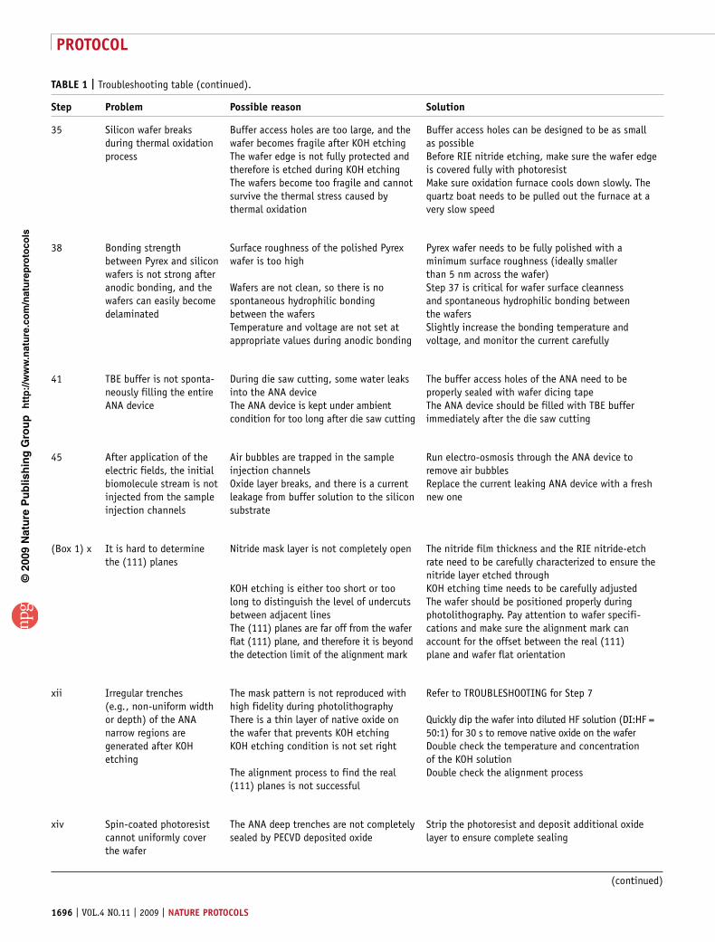
taBle 1 | Troubleshooting table.
step problem possible reason solution
3 Spin-coated photoresist is not uniform and has traces of particulates and particles
Amount of photoresist is not enough Air bubbles are generated during dispensing Wafer surface is not clean
Make sure enough photoresist is dispensed in the middle of the wafer before spin coating Make sure no air bubble is trapped in photoresist before dispensing Re-clean wafer with the Piranha solution. If still not clean, use a fresh wafer directly out of a new wafer box
7 Photoresist pattern on the wafer does not reproduce the photomask features with good fidelity
Photoresist is under- or overexposed Photoresist is under- or overdeveloped The photomask is contaminated
The exposure dose and development time need to be better characterized The thickness of the photoresist layer needs to be monitored after spin coating for consistency Gently clean the photomask with solvents and then blow dry with N2
14, 17, 18
After RIE process, some black silicon appears on the etched area
Photoresist residue is left after development There is a thin layer of native oxide on the silicon wafer RIE machine chamber is not clean and has an accumulation of organic residue
Hard bake the wafer at 120 °C for additional 30 min before the RIE step Make sure to perform Steps 11–13. They are critical to ensure no black silicon etching to occur during the RIE process
28 KOH-etch rate for silicon is slow and not uniform across the entire wafer
Temperature of the KOH solution is low or the KOH concentration is not set right There is a layer of native oxide on the silicon wafer that prevents KOH etching The silicon nitride mask layer is not completely etched through during the RIE step There exists a loading effect during KOH etching
Double check the temperature and concentration of the KOH solution Quickly dip the wafer into a diluted HF solution (DI:HF = 50:1) for 10 s to remove native oxide on the wafer The thickness of the nitride film and the RIE nitride-etch rate need to be carefully characterized to ensure the nitride layer etched through. Step 27 is critical for this purpose Rotate the wafer for 90° every hour during KOH etching
(continued)
1696 | VOL.4 NO.11 | 2009 | nature protocols
p
uor
G g
n ih si l
bu
P eru ta
N 900 2©
nat
ure
pro
toco
ls/
moc. e r
ut an .
ww
w / /:pt t
h
protocol
taBle 1 | Troubleshooting table (continued).
step problem possible reason solution
35 Silicon wafer breaks during thermal oxidation process
Buffer access holes are too large, and the wafer becomes fragile after KOH etching The wafer edge is not fully protected and therefore is etched during KOH etching The wafers become too fragile and cannot survive the thermal stress caused by thermal oxidation
Buffer access holes can be designed to be as small as possible Before RIE nitride etching, make sure the wafer edge is covered fully with photoresist Make sure oxidation furnace cools down slowly. The quartz boat needs to be pulled out the furnace at a very slow speed
38 Bonding strength between Pyrex and silicon wafers is not strong after anodic bonding, and the wafers can easily become delaminated
Surface roughness of the polished Pyrex wafer is too high Wafers are not clean, so there is no spontaneous hydrophilic bonding between the wafers Temperature and voltage are not set at appropriate values during anodic bonding
Pyrex wafer needs to be fully polished with a minimum surface roughness (ideally smaller than 5 nm across the wafer) Step 37 is critical for wafer surface cleanness and spontaneous hydrophilic bonding between the wafers Slightly increase the bonding temperature and voltage, and monitor the current carefully
41 TBE buffer is not sponta-neously filling the entire ANA device
During die saw cutting, some water leaks into the ANA device The ANA device is kept under ambient condition for too long after die saw cutting
The buffer access holes of the ANA need to be properly sealed with wafer dicing tape The ANA device should be filled with TBE buffer immediately after the die saw cutting
45 After application of the electric fields, the initial biomolecule stream is not injected from the sample injection channels
Air bubbles are trapped in the sample injection channels Oxide layer breaks, and there is a current leakage from buffer solution to the silicon substrate
Run electro-osmosis through the ANA device to remove air bubbles Replace the current leaking ANA device with a fresh new one
(Box 1) x It is hard to determine the (111) planes
Nitride mask layer is not completely open KOH etching is either too short or too long to distinguish the level of undercuts between adjacent lines The (111) planes are far off from the wafer flat (111) plane, and therefore it is beyond the detection limit of the alignment mark
The nitride film thickness and the RIE nitride-etch rate need to be carefully characterized to ensure the nitride layer etched through KOH etching time needs to be carefully adjusted The wafer should be positioned properly during photolithography. Pay attention to wafer specifi-cations and make sure the alignment mark can account for the offset between the real (111) plane and wafer flat orientation
xii Irregular trenches (e.g., non-uniform width or depth) of the ANA narrow regions are generated after KOH etching
The mask pattern is not reproduced with high fidelity during photolithography There is a thin layer of native oxide on the wafer that prevents KOH etching KOH etching condition is not set right The alignment process to find the real (111) planes is not successful
Refer to TROUBLESHOOTING for Step 7 Quickly dip the wafer into diluted HF solution (DI:HF = 50:1) for 30 s to remove native oxide on the wafer Double check the temperature and concentration of the KOH solution Double check the alignment process
xiv Spin-coated photoresist cannot uniformly cover the wafer
The ANA deep trenches are not completely sealed by PECVD deposited oxide
Strip the photoresist and deposit additional oxide layer to ensure complete sealing
(continued)

nature protocols | VOL.4 NO.11 | 2009 | 1697
p
uor
G g
n ih si l
bu
P eru ta
N 900 2©
nat
ure
pro
toco
ls/
moc. e r
ut an .
ww
w / /:pt t
h
protocol
antIcIpateD resultsThe stream deflection pattern during separation depends on the separation mechanisms applied in the ANA. For Ogston sieving, smaller molecules will assume a larger steam deflection angle in the ANA and will be collected by the microfluidic channels on the right-hand side of the ANA opposite edge. In contrast, for entropic trapping, as longer molecules assume a greater deflection angle in the ANA, they will be deflected towards the right-hand side of the ANA opposite edge and collected by the microfluidic channels. For electrostatic sieving, the separation pattern would be more difficult to predict. In principle, smaller biomolecules bearing less negative charges will be deflected more in the ANA, towards the right-hand side of the ANA opposite edge.
During separation, we can use the CCD camera attached to the microscope to visualize and record the migration trajec-tories of fluorescence-labeled biomolecules in the ANA. These fluorescence images can be further analyzed with the image processing software (e.g., IPLab, BD Biosciences Bioimaging, Rockville, MD, USA) to generate fluorescence intensity profiles. Gaussian functions can be used for fitting these fluorescence intensity profiles to determine means (the maximum intensity) and widths of the fractionated biomolecule streams19. The separation efficiency of the ANA can then be further quantified by calculating both the size selectivity and the effective peak capacity under different electric field conditions22. Figures 3e–f shows examples of composite fluorescent photographs of continuous-flow separation of proteins (Fig. 3e) and DNA (Fig. 3f) through both the planar and the vertical ANA, respectively. Upon application of the electric field Ey along the y axis of the ANA, the initial biomolecule stream is continuously injected into the deep (for the planar ANA) or wide (for the vertical ANA) channels on the top left of the ANA structure (Fig. 3f (i)). After the orthogonal electric field Ex is superimposed along the x-axis across the nanofilters, the drifting biomolecules in the deep channels start to jump across the nanofilters and separate from each other (Fig. 3f (ii and iii)). With properly adjusted values of both Ex and Ey, both the protein mixtures and the long DNA digest can be based-line separated into distinct streams within a few minutes (Fig. 3e–f). The sample volume throughput of the ANA structure can be estimated based on the migration speed of biomolecules in the ANA and the dimensions of the ANA sample injection channels. For the protein separation shown in Figure 3e, the sample volume throughputs for the planar and vertical ANA are in the range of nl h − 1 and µl h − 1, respectively. The sample throughput of the ANA can be scaled up by parallelism with multi-device processing. For the vertical ANA, the sample throughput can be further enhanced by increasing the depth of the ANA structure to a maximum value of the silicon wafer’s thickness, which is about 500 µm for a 6-inch wafer.
taBle 1 | Troubleshooting table (continued).
step problem possible reason solution
xviii DRIE etching does not reproduce the features on the mask with good fidelity
Severe undercuts occur during DRIE process The etch mask (i.e., the photoresist layer) is etched away during DRIE process
Double check the DRIE etch recipe. If necessary, adjust the etching parameters to minimize undercuts Use a thicker layer of photoresist or switch to an oxide mask layer if very deep silicon etching is desired
xxv The final gap size of the ANA narrow regions is either too small or too large
Thickness of the thermal oxide layer is not controlled well Depth of the ANA wide channels is different from of the ANA narrow channels Nitride mask layer is not completely removed, or there is some Teflon-like polymer left in the deep trenches after the DRIE process
Double check thermal oxidation conditions such as temperature and gas flows. Run thermal oxidation again if more oxide deposition is desired Take cross-sectional SEM of the ANA device to make sure the depths of the ANA narrow and wide regions are the same. Otherwise, further adjustment of the respective etching time is required Immerse the wafer in the HF solution for a longer period to strip the nitride mask layer completely. Run oxygen plasma for a longer time to remove the polymer layer
ANA, anisotropic nanofluidic-filter (nanofilter) array; DI, deionized and distilled water; DRIE, deep reactive ion etching; HF, hydrofluoric acid; PECVD, plasma-enhanced chemical vapor deposition; RIE, reactive ion etching; SEM, scanning electron microscopy.
Note: Supplementary information is available via the HTML version of this article.
acknowleDGMents The authors acknowledge financial support from the National Institute of Health (EB005743), Korea Institute of Science and Technology–Intelligent Microsystems Center (KIST-IMC), and the Singapore-MIT Alliance (SMA-II, CE program). We also thank J. Yoo for his contribution in the experimental setup and H. Bow and S. Reto for helpful discussions.
The MIT Microsystems Technology Laboratories is acknowledged for support in microfabrication.
autHor contrIButIons J.F., P.M. and J.H. conceived and designed the ANA chips. J.F. and P.M. fabricated the ANA chips. J.F. and P.M. designed and performed experiments, and analyzed data. J.F. and P.M. wrote manuscript.

1698 | VOL.4 NO.11 | 2009 | nature protocols
p
uor
G g
n ih si l
bu
P eru ta
N 900 2©
nat
ure
pro
toco
ls/
moc. e r
ut an .
ww
w / /:pt t
h
protocol
Published online at http://www.natureprotocols.com. Reprints and permissions information is available online at http://npg.nature.com/ reprintsandpermissions.
1. Goodsell, D.S. Bionanotechnology, Lessons from Nature (Wiley-Liss, Hoboken, New Jersey, 2004).
2. Jain, K.K. Nanobiotechnology in Molecular Diagnostics, Current Techniques and Applications (Horizontal Bioscience, Norfolk, UK, 2006).
3. Chu, S. Biology and polymer physics at the single-molecule level. Philos. Trans. R. Soc. London Ser. A-Math. Phys. Eng. Sci. 361, 689–693 (2003).
4. Fortina, P., Kricka, L.J., Surrey, S. & Grodzinski, P. Nanobiotechnology: the promise and reality of new approaches to molecular recognition. Trends Biotechnol. 23, 168–173 (2005).
5. Hinterdorfer, P. & Dufrêne, Y.F. Detection and localization of single molecular recognition events using atomic force microscopy. Nature Methods 3, 347–355 (2006).
6. Eijkel, J.C.T. & van den Berg, A. Nanofluidics: what is it and what can we expect from it? Microfluid. Nanofluid. 1, 249–267 (2005).
7. Craighead, H. Future lab-on-a-chip technologies for interrogating individual molecules. Nature 442, 387–393 (2006).
8. Tegenfeldt, J.O et al. Micro- and nanofluidics for DNA analysis. Anal. Bioanal. Chem. 378, 1678–1692 (2004).
9. Han, J., Fu, J. & Schoch, R.B. Molecular sieving using nanofilters: past, present and future. Lab Chip 8, 23–33 (2008).
10. Fu, J., Mao, P. & Han, J. Artificial molecular sieves and filters: a new paradigm for biomolecule separation. Trends Biotech. 26, 311–320 (2008).
11. Slater, G.W. Theory of DNA electrophoresis: a look at some current challenges. Electrophoresis 21, 3873–3887 (2000).
12. Whitesides, G.M. The origins and the future of microfluidics. Nature 442, 368–373 (2006).
13. El-Ali, J., Sorger, P.K. & Jensen, K.F. Cells on chips. Nature 442, 403–411 (2006).
14. Han, J. & Craighead, H.G. Separation of long DNA molecules in a microfabricated entropic trap array. Science 288, 1026–1029 (2000).
15. Huang, L.R. et al. A DNA prism: high-speed continuous fractionation of large DNA molecules. Nature Biotech. 20, 1048–1051 (2002).
16. Baba, M. et al. DNA size separation using artificially nanostructured matrix. Appl. Phys. Lett. 83, 1468–1470 (2003).
17. Kaji, N. et al. Separation of long DNA molecules by quartz nanopillar chips under a direct current electric field. Anal. Chem. 76, 15–22 (2004).
18. Huang, L.R., Cox, E.C., Austin, R.H. & Sturm, J.C. Continuous particle separation through deterministic lateral displacement. Science 304, 987–990 (2004).
19. Fu, J., Schoch, R.B., Bow, H., Stevens, A.L., Tannenbaum, S.R. & Han, J. A patterned anisotropic nanofluidic sieving structure for continuous-flow separation of DNA and proteins. Nature Nanotech. 2, 121–128 (2007).
20. Mao, P. & Han, J. Massively-parallel ultra-high-aspect-ratio nanochannels as mesoporous membranes. Lab Chip 9, 586–591 (2009).
21. Scopes, R.K. Protein Purification, Principles and Practice, ed. 3 (Springer-Verlag, New York, 1993).
22. Giddings, J.C. Dynamics of Chromatography. Part 1. Principles and Theory (Marcel Dekker, New York, 1965).
23. Yao, G. et al. SDS capillary gel electrophoresis of proteins in micro-fabricated channels. Proc. Natl. Acad. Sci. USA 96, 5372–5377 (1999).
24. Callewaert, N. et al. Total serum protein N-glycome profiling on a capillary electrophoresis-microfluidics platform. Electrophoresis 25, 3128–3131 (2004).
25. Turner, S.W., Perez, A.M., Lopez, A. & Craighead, H.G. Monolithic nanofluid sieving structures for DNA manipulation. J. Vac. Sci. Technol. B 16, 3835–3840 (1998).
26. Cao, H. et al. Fabrication of 10 nm enclosed nanofluidic channels. Appl. Phys. Lett. 81, 174–176 (2002).
27. Fu, J., Mao, P. & Han, J. Nanofilter array chip for fast gel-free biomolecule separation. Appl. Phys. Lett. 87, 263902 (2005).
28. Fu, J., Yoo, J. & Han, J. Molecular sieving in periodic free-energy landscapes created by patterned nanofilter arrays. Phys. Rev. Lett. 97, 018103 (2006).
29. Eijkel, J.C.T. & van den Berg, A. Nanotechnology for membranes, filters and sieves. Lab Chip 6, 19–23 (2006).
30. Austin, R. Nanofluidics: a fork in the nano-road. Nature Nanotech. 2, 121–128 (2007).
31. Pamme, N. Continuous flow separations in microfluidic devices. Lab Chip 7, 1644–1659 (2007).
32. Wulfkuhle, J.D., Liotta, L.A. & Petricoin, E.F. Proteomic applications for the early detection of cancer. Nat. Rev. Cancer 3, 267–275 (2003).
33. Righetti, P.G., Castagna, A., Herbert, B., Reymond, F. & Rossier, J.S. Prefractionation techniques in proteome analysis. Proteomics 3, 1397–1407 (2003).
34. Mao, P. & Han, J. Fabrication and characterization of 20-nm nanofluidic channels by glass-glass and glass-silicon bonding. Lab Chip 5, 837–844 (2005).
35. Bow, H., Fu, J. & Han, J. Decreasing effective nanofluidic filter size by modulating electrical double layers: separation enhancement in microfabricated nanofluidic filters. Electrophoresis 29, 4646–4651 (2008).
36. Huang, L.R. et al. Generation of large-area tunable uniform electric fields in microfluid arrays for rapid DNA separation. Tech. Dig. Int. Elect. Dev. Mtg. 363–366 (2002).