chapter 5 simulation of diodes for …shodhganga.inflibnet.ac.in/bitstream/10603/6514/10/10_chapter...
TRANSCRIPT

107
CHAPTER 5
SIMULATION OF DIODES FOR MOLECULAR
ELECTRONIC LOGIC CIRCUITS
5.1 INTRODUCTION
Recently, there have been significant advances in the fabrication and
demonstration of molecular electronic wires and or molecular electrons
diodes, two-terminal electrical switches made from single molecules. There
also have been advances in techniques for making reliable electrical contact
with such electrically conducting molecules. These promising developments in
the field of nano electronics suggest that it must be possible to build and to
demonstrate somewhat more complex molecular electronic structures that
would include two or three molecular electronic diodes that would perform as
digital logic circuits.
In this chapter we modeled the electron transport characteristic of
rectifying diodes based on Aviram and Ratner model [47].
A detailed analysis on the effect of the electron transfer path between
the donor and acceptor, has been carried out through frontier molecular orbital
analysis.
5.2 AVIRAM AND RATNER MODEL
The seminal work of Aviram and Ratner in 1974 led to several
experimental attempts to build molecular diodes. Aviram and Ratner have
suggested [37] that electron donating constituents make conjugated molecular
groups having a large electron density (N-type) and electron withdrawing

108
constituents make conjugated molecular groups poor in electron density
(P-type). According to them, a noncentrosymmetric molecule having
appropriate donor and acceptor moieties linked with a s-bridge and connected
with suitable electrodes will conduct current only in one direction - acting as a
rectifier. They showed that in this molecule, the lowest unoccupied molecular
orbital (LUMO) and highest occupied molecular orbital (HOMO) can be
aligned in such a way that electronic conduction is possible only in one
direction making it function like a molecular diode exhibiting the transport
characteristic as in Figure 5.1. Asymmetric current-voltage characteristics for
a s- bridged system were first reported in 1990 [98,99]
The band diagram of the mono-molecular diode under zero-bios
conditions is shown in Figure 5.2. We notice that there are three potential
barriers - one corresponding to the insulating group (middle barrier) and two
corresponding to the contact between the molecule and the electrode (left and
right barriers). These potential barriers provide the required isolation between
various parts of the structure. The occupied energy levels in the metal contacts
and the Fermi energy level EF are also shown. On the left of the central barrier
all the pi-type energy levels (HOMO as well as LUMO) are elevated due to
the presence of the electron donating group X and similarly on the right of the
central barrier the energy levels are lowered due to the presence of the electron
withdrawing group Y. This causes a built-in potential to develop across the
barrier represented by the energy difference ΔELUMO.

109
Figure 5.1(a) Schematic representation of molecular rectifier
Figure 5.1(b) Ideal I-V characteristic of a molecular diode
I
V

110
Figure 5.2 Molecular diode orbital energy diagram under zero bias condition
Figure 5.3. Molecular diode orbital energy diagram under forward and reverse bias conditions
Donor (D)
Acceptor (A) Au
Au
ΔELUMO
Energy
Distance
Zero applied bias Femi Energy
Energy
Energy
Distance
Tra
nsm
itted
E
lect
rons
Cur
rent
(Hol
es)
Forward Bias
Reverse Bias
Distance
No Current
111
In a proper applied bias voltage, electron tunneling occurs from the
acceptor part of the molecule to the donor part, through the unoccupied
manifold of the molecular orbitals. When such a molecule is connected
through two electrodes (acceptor part connected to the cathode and donor part
connected to the anode) and a proper forward bias (at least it should be
sufficient enough to raise the Fermi energy of the electron in the occupied
level of gold contact on the acceptor side to that of the energy of the LUMO
localized on the acceptor part of the molecule) is applied, then the electron can
flow from the gold contact to the LUMO, localized on the acceptor part. The
injected electron from the gold contact to the acceptor part of the molecule can
now tunnel through the central insulating bridge to the higher unoccupied
molecular orbital localized in the donor half of the molecule and finally
escapes into the gold contact lying in the donor part. In analogy to the forward
bias condition, in a reverse applied bias, for electron transfer to occur from the
donor part of the molecule to the acceptor part through the central insulating
bridge, the reverse bias must be sufficient to raise the Fermi energy of the gold
contact on the donor side of the molecule so that it is at least as high as the
energy of the empty orbital localized on the donor part of the molecule.
According to Ellenbogen and Love [100], during the process of applied bias in
the forward and reverse bias conditions, energy level alignment occurs in the
molecule which is responsible for a feasible electron transfer process in the
forward bias condition compared to reverse biased condition (reverse bias
process requires more energy than for the forward bias), and thus rectification
occurs.
The band diagram under reverse bias conditions (left hand contact at
lower potential than the right hand contact) is shown in Figure 5.3. As a result,
electrons from the left contact would try to flow towards the right contact
which is at a higher potential. However, conduction is not possible because the
there is still an energy difference between the Fermi energy EF of the left

112
contact and the LUMO energy of the electron donor doped section. It is
assumed that both the applied forward and reverse bias potentials are identical.
For a higher reverse bias, however, it is possible for the Fermi energy EF of the
left contact to come in resonance with the LUMO energy of the electron donor
doped section causing a large current to flow in reverse direction and this is
akin to the breakdown condition in a diode.
5.3 RECTIFYING DIODE
Based on the model discussed in the previous section, we propose the
diode structure as shown in Figure 5.4 consisting of two identical sections
(S1, S2) separated by an insulating group R. Section S1 is doped by NH2
donating group (X ) and section S2 is doped by NO2 electron withdrawing
group (Y ). The insulating group CH2CH2 (R) is incorporated into the
molecular wire.. The single molecule ends are connected to the contact
electrodes e.g. gold. For current to flow electrons must overcome the potential
barrier from electron acceptor doped section (S2) to electron donor doped
section (S1) and this forms the basis for the formation of the mono-molecular
rectifying diode.
Figure 5.4 Optimized Geometry of diode molecule-I (Level: B3 PW91/6-31G)

113
Figure 5.5 Current-voltage characteristics of diode molecule-I
Figure 5.6 Conductance-voltage characteristics of diode molecule-I

114
The rectifying ratio is the parameter that shows the amount of
rectification. As seen in Figure 5.5, the rectifying ratio of this molecule is 1.75
By choice of (X) and (Y) groups this value can be improved.
As discussed earlier in the principle of electrical rectification, the most
important thing for a D-S-A molecule to show rectification is that it should
have the localized orbitals in different parts of the molecule, which will be
helpful in tunneling of electron at a proper applied bias. For visualization of
the orbital population density, population analysis of molecule 1 has been
carried out at its B3PW91/6-31G* optimized geometry and the corresponding
few frontier molecular orbitals (FMO)s are shown in Figure 5.7-5.11.
It is observed that the molecule when connected in the circuit, LUMO
& LUMO+2 will be channel for the electron transport i.e., in a proper applied
bias voltage, the tunneling of electron will occur from LUMO to LUMO+2. At
this applied bias, resonance (energy level alignment) between the LUMO &
LUMO+2 and also coupling between the two levels occurs. Visualizing the
two orbitals, it can be expected that a constructive electronic coupling between
LUMO & LUMO+2 can occur at the backbone and ring junctions to make the
process of electron tunneling feasible. During the reverse bias condition,
electron will be injected to LUMO+2 of the donor side and the process of
tunneling will occur at higher applied voltage compared to forward bias
condition because of the energy level alignments.

115
Figure 5.7 Frontier molecular orbital HOMO diagram of diode molecule
Figure 5.8 Frontier molecular orbital HOMO-1 diagram of diode molecule
HOMO
HOMO-1

116
Figure 5.9 Frontier molecular orbital LUMO diagram of diode molecule
Figure 5.10 Frontier molecular orbital LUMO+1 diagram of diode molecule
Figure 5.11 Frontier molecular orbital LUMO+2 diagram of diode molecule-I
LUMO
LUMO+1
LUMO+2

117
5.4 DEVICE CHARACTERISTICS OF DIODE MOLECULE-II
Figure 5.12 Optimized geometrical structure of diode molecule II obtained
from the B3PW91/6-31G*
In the following work we design a new intramolecular complex with
donor and acceptor molecular subunits and to explore the possibility of its
working as a diode.
Figure 5.12 shows the optimized geometry of the diode molecule-II.
In particular, we have substituted OCH3 and CN group in the benzene
ring, among the different combinations of donor (OCH3, CH3, NH2) and
acceptor (CN, CF3, NO2). On the basis of the above results, it is of interest to
investigate the electronic structure for a combined molecular complex of these
subunits. An aliphatic group like methylene CH2 or dimethylene CH2 CH2 is
required to be attached between the n-type and p-type molecules to act like a
spacer and form a potential barrier to electron transport across the molecule.
Accordingly, we have decided to use spacers such as CH2 or CH2CH2 between
the donor and acceptor subunits to form an intramolecular donor spacer
acceptor (D-S-A) rectifier. The molecule is attached to two gold leads.

118
Figure 5.13 Current - voltage characteristics of diode molecule-II
Figure 5.14 Conductance - voltage characteristics of diode molecule-II

119
Figure 5.13 shows the calculated I-V curves, which show that the
device acts as an effective molecular diode. Thus, the current is mostly small,
until the bias voltage approaches 1V, at which point the current begins to rise
steeply.
As quoted before the choice of (X) and (Y) groups can change the
rectifying ratio, the rectifying ratio of this molecule is 1.5. This seen in
Figure 5.13 and Figure5.14.
The workings of this device can be understood from a straightforward
analysis of the molecular levels of the device. For the most part, the donor and
the acceptor portions of the molecule have levels that are well separated from
each other. Hence, electrons tunneling through the CH2 barrier have nowhere
to go, and so the current is small. However, under the influence of a bias of
about 1V, the levels are shifted into alignment. Electrons can therefore tunnel
through these levels and then into the device electrodes signaled by the
subsequent current rise.
For an active device like diode one needs to control the flow of
electrons to obtain the desired electronic properties. In the case of benzene
molecule substituted by an electron donating group, the π electron density is
enhanced and the molecular energy levels typically orient in such a way that
the electrons can flow in one direction while the other direction the flow of
electrons is blocked the frontier molecular orbitals of the molecule under
investigation are plotted from orbitals population densities obtained from the
optimized structure and are presented in figure 5.15, 5.16 and 5.17
The analysis shows stabilized HOMOs and LUMOs. Due to this, this
molecule has lower value of potential barrier . To show electrical rectification,
the molecular energy levels typically orient in such a way that the electrons
can flow in one direction while the other direction the flow of electrons is
blocked.

120
Figure 5.15 Frontier molecular LUMO orbital diagram of
diode molecule-II
Figure 5.16 Frontier molecular orbital LUMO+1 diagram
of diode molecule-II
Figure 5.17 Frontier molecular orbital HOMO diagram of diode molecule-II

121
5.5 NEGATIVE DIFFERENTIAL RESISTANCE IN MOLECULAR
JUNCTIONS
The discovery of negative differential resistance (NDR) in
semiconductor diode has opened a new chapter in device technology. Through
the use of NDR devices circuits with complicated function can be
implemented with significantly fewer components.
The negative differential resistance is observed in ethynyl phenyl
based organic molecules at room temperatures [82]
We have used a molecule consisting of three aromatic phenyl rings in
series. The two hydrogen atoms of the middle ring are substituted by acceptor
group NO2 and donor group NH2, while the whole molecule is chemisorbed
onto the contact surfaces of gold leads. The optimized geometry is shown in
Figure 5.18
Figure 5.18 Optimized geometrical structure NDR molecule

122
Table 5.1 Geometrical parameters (angle) for NDR molecule
Definition Value (degrees) Definition Value (degrees)
C2,C1,C6 118.6052 C18,C19,S39 119.4471
C2,C1,N11 120.8071 C20,C19,S39 119.9428
C6,C1,N11 120.5876 C19,C20,C21 119.6668
C1,C2,C3 120.7142 C19,C20,H25 119.7494
C1,C2,H7 119.4879 C21,C20,H25 120.5833
C3,C2,H7 119.7978 C20,C21,C22 120.0782
C2,C3,C4 119.6124 C20,C21,H26 120.6236
C2,C3,H16 121.2279 C22,C21,H26 119.2978
C4,C3,H16 119.1596 C17,C22,C21 119.9405
C3,C4,C5 120.7446 C17,C22,H27 120.988
C3,C4,N10 119.6106 C21,C22,H27 119.0707
C5,C4,N10 119.6449 H16,H27,C22 158.5336
C4,C5,C6 119.7394 C29,C28,C33 119.4579
C4,C5,H8 119.137 C29,C28,H34 120.3406
C6,C5,H8 121.1236 C33,C28,H34 120.1976
C1,C6,C5 120.5841 C28,C29,C30 120.3802
C1,C6,H9 119.4796 C28,C29,H35 119.4409
C5,C6,H9 119.9362 C30,C29,H35 120.176
C6,H9,H36 145.8164 C29,C30,C31 119.7356
C4,N10,O12 118.4752 C29,C30,H36 120.1553
C4,N10,O13 118.4228 C31,C30,H36 120.1091
O12,N10,O13 123.1021 C30,C31,C32 120.337
C1,N11,H14 120.7991 C30,C31,H37 120.2221
C1,N11,H15 121.5765 C32,C31,H37 119.4395
H14,N11,H15 117.6085 C31,C32,C33 119.4697
C3,H16,H27 112.8626 C31,C32,H38 119.9467
C18,C17,C22 120.237 C33,C32,H38 120.5834
C18,C17,H23 119.5735 C28,C33,C32 120.6123
C22,C17,H23 120.1895 C28,C33,S40 117.7412
C17,C18,C19 119.5141 C32,C33,S40 121.6219
C17,C18,H24 120.7495 H9,H36,C30 40.228
C19,C18,H24 119.7364 C19,S39,H41 97.1422
C18,C19,C20 120.5569 C33,S40,H42 97.0493

123
Table 5.2 Geometrical parameters (distance) for NDR molecule
Definition Value (Angstroms) Definition Value (Angstroms)
C1,C2 1.4178 C18,C19 1.3971
C1,C6 1.418 C18,H24 1.0847
C1,N11 1.3637 C19,20 1.3978
C2,C3 1.3829 C19,39 1.8554
C2,H7 1.0856 C20,C21 1.3985
C3,C4 1.401 C20,C25 1.0849
C3,H16 1.0828 C21,C22 1.3986
C4,C5 1.4015 C21,H26 1.0853
C4,N10 1.4341 C22,H27 1.0847
C5,C6 1.3827 C28,C29 1.3979
C5,H8 1.0828 C28,C33 1.3976
C6,H9 1.0849 C28,H34 1.0846
H9,H36 4.982 C29,C30 1.3975
N10,O12 1.2665 C29,H35 1.0852
N10,O13 1.267 C30,C31 1.3977
N11,H14 1.0055 C30,H36 1.0848
N11,H15 1.0106 C31,C32 1.3982
O12,H26 3.3241 C31,H37 1.0853
H16,H27 4.8041 C32,C33 1.3981
C17,C18 1.3992 C32,H38 1.0855
C17,C22 1.3977 C33,S40 1.8475
C17,H23 1.086 S39,H41 1.3797
S40,H42 1.3737
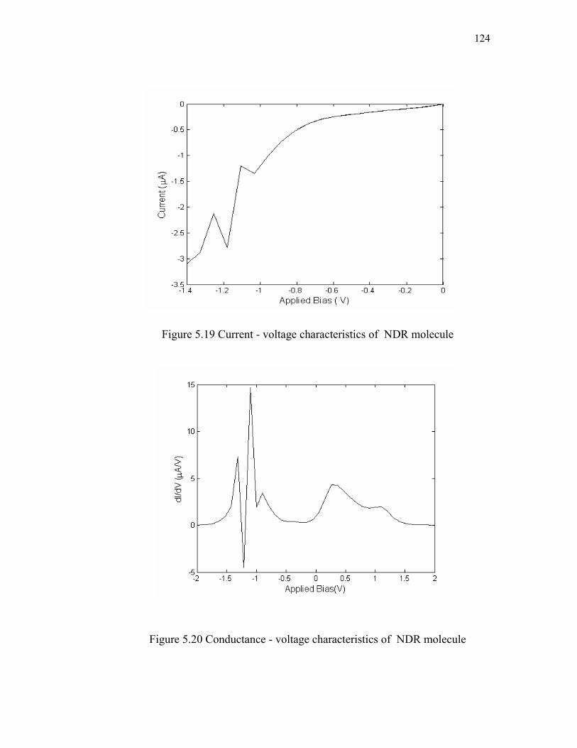
The calculated I-V and G-V characteristics are shown in Figure 5.19
and 5.20. The current voltage characteristics show negative differential
resistance (NDR), which is drop, in the current with increase in voltage in one
direction of the applied voltage. The benzene molecule containing a electron
withdrawing nitro group (NO2), and electron rich amino (NH2) exhibits this
property.
124
Figure 5.19 Current - voltage characteristics of NDR molecule
Figure 5.20 Conductance - voltage characteristics of NDR molecule

125
Figure 5.21 Frontier molecular orbital HOMO diagram of NDR molecule
Figure 5.22 Frontier molecular orbital HOMO-1 diagram of NDR molecule
Figure 5.23 Frontier molecular orbital HOMO-2 diagram of NDR molecule
126
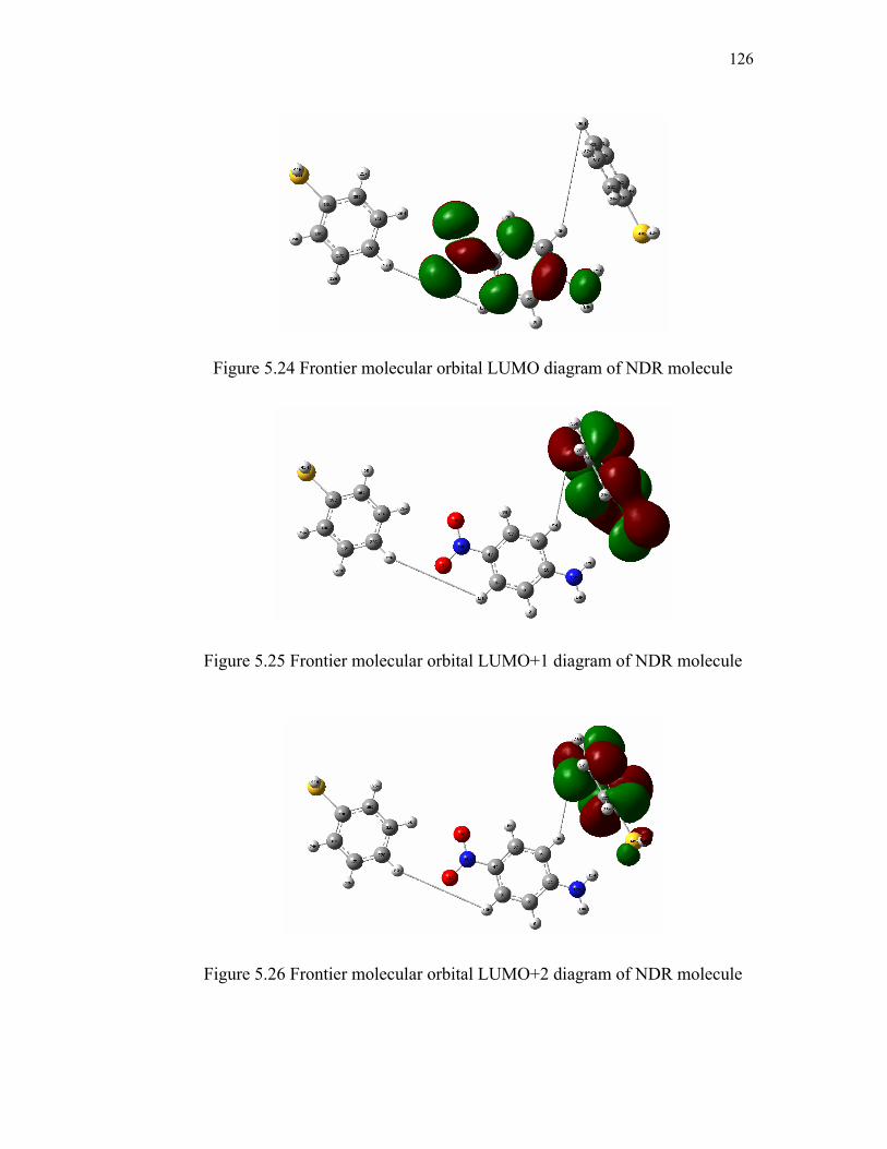
Figure 5.24 Frontier molecular orbital LUMO diagram of NDR molecule
Figure 5.25 Frontier molecular orbital LUMO+1 diagram of NDR molecule
Figure 5.26 Frontier molecular orbital LUMO+2 diagram of NDR molecule
127
To understand the electron transport through this molecule we have
analysed the spacial extent of the frontier orbitals (HOMO, LUMO), which
provides a strategy by which the rectifying properties of this molecular system
can be understood. The Figures 5.21, 5.22 and 5.23 show HOMO – k
(k= 0,1,2) and plots of Figure 5.24, 5.25 and 5.26 show LUMO + k (k- 0,1,2)
plots of the molecule. It is observed that while the HOMO -1 and HOMO -2
are localized at the ring 1, the LUMO+1 and LUMO +2 are localized at the
ring3. Both HOMO and LUMO at k=0 are localized on the middle ring.
Therefore in this device electrons are injected from cathode to the LUMO state
on the ring3. The incoming electron of the ring3 is then transferred to the
unoccupied orbital localized on ring1.
Diode-like behavior of the asymmetric molecular complex is not
observed in the case when charging is completely neglected. Within our
model, the mentioned phenomenon is a combined effect of the asymmetric
structure of molecule itself and the charging profile. Current rectification is
due to the presence of chemical substituent groups and their influence on
charge redistribution within the molecular system. Since the location of
substituent is spatially asymmetric with respect to the direction of the current
flow, the response upon the applied bias is also asymmetric in the case of non-
zero charging.
5.6 SUMMARY
The electron transport characteristic of rectifying diodes based on
Aviram Ratner model is investigated. The diode is formed by two sections,
one doped with NH2 and other with NO2 separated by an insulating CH2CH2
group. The current in forward bias of 4V is 8µA and at reverse bias 0f-4V is
4.The rectifying ratio is 1.75. Similar asymmetric behavior is also observed on
a molecular diode reported in [106] using MCBJ setup. The experiment is
focused on 1V measurements at a temperature of 30k, showing clearly

128
asymmetric behavior. We have also substituted OCH3 and CN group in the
benzene ring with CH2 as tunneling barrier. This donor-spacer-acceptor shows
a rectifying ratio of 1.5.