chapter 3-part-1
TRANSCRIPT

EE603 – CMOS INTEGRATED CIRCUIT DESIGN
CHAPTER 3 PART 1:CHAPTER 3 PART 1:The DevicesThe Devices

Upon completion Understand diode basic concept
- Depletion region- Ideal diode equation
Explain design abstraction level- System- Module - Gate- Circuit- Device

Majority and Minority Carriers In an n-type material - electron is called majority carrier and hole
the minority carrier In a p-type material – hole is majority carrier and electron is the
minority carrier

Semiconductor Diode Diode is formed by bringing these two material together p- and n-
type Electrons and holes at joined region will combine, resulting in a
lack of carriers in the region near the junction (depletion region)

The Diode
n
p
p
n
B A SiO2Al
A
B
Al
A
B
Cross-section of pn-junction in an IC process
One-dimensionalrepresentation diode symbol
Mostly occurring as parasitic element in Digital ICs

Depletion Region
hole diffusionelectron diffusion
p n
hole driftelectron drift
ChargeDensity
Distancex+
-
ElectricalxField
x
PotentialV
ξ
ρ
W2-W1
ψ0
(a) Current flow.
(b) Charge density.
(c) Electric field.
(d) Electrostaticpotential.

Semiconductor Diode Since the diode is two-terminal device,
the application of a voltage across its terminals leaves three possibilities: No bias (VD = 0V)
Forward bias (VD > 0V)
Reversed bias (VD < 0V)
Each condition will result in a response

No Applied Bias (VD = 0V) Under no-bias conditions, any minority carries (holes) in the n-type
material find themselves within the depletion region will pass directly into p-type material
Majority carriers (electrons) of n-type material must overcome the attractive forces of the layer of positive ions in n-type material and the shield of negative ions in p-type material to migrate into the area beyond the depletion region of p-type material.
In the absence of an applied bias voltage, the net flow of charge in any one direction for semiconductor diode is zero

No Applied Bias (VD = 0V)
Figure 1.14 p-n junction with no external bias

No Applied Bias (VD = 0V)

Reverse-Bias Condition (VD < 0V) The number of uncovered positive ions in the depletion region of n-type
will increase due to large number of free electrons drawn to the positive potential
The number of uncovered negative ions will increase in p-type resulting widening of depletion region
This region established great barrier for the majority carriers to overcome – resulting Imajority = 0
The number pf minority carriers find themselves entering the depletion region will not change resulting in minority-carrier flow vectors of the same magnitude
The current exists under reverse-bias conditions is called the reverse saturation current and represented by Is
Therefore, ID= -Is

Reverse-Bias Condition (VD < 0V)
Figure 1-16 Reverse-biased p-n junction

Reverse-Bias Condition (VD < 0V)

Forward-Bias Condition (VD = 0V)
A semiconductor diode is forward-biased when the association p-type and positive and n-type and negative has been established
The application of forward-bias potential will pressure the electrons in n-type and hole in p-type to recombine with ions near the boundary and reduce the width of depletion region
The resulting minority-carrier flow of electrons from p-type to n-type has not changed in magnitude, but the reduction in width of depletion region has resulted in a heavy majority flow across the junction

Forward-Bias Condition (VD = 0V)
Figure 1.18 Forward-biased p-n junction

For Forward-bias and Reverse-bias
(1.4)

Figure 1.19 Silicon semiconductor diode characteristics

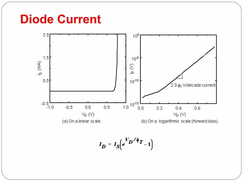
Diode Current
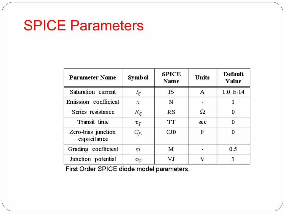
SPICE Parameters

Hierarchy Design
Definition : Hierarchy design is a technique involves dividing a module into sub-
modules and then repeating this operation on the sub-modules until the complexity of the smaller parts becomes manageable.
The hierarchical design approach reduces the design complexity by dividing the large system into several sub-modules. All of the blocks in the sub-modules can be combined with ease at the end of the design process, to form the large system.

Hierarchy Design – Cont’d
This approach is very similar to the software case where large programs are split into smaller and smaller sections until simple subroutines, with well-defined functions and interfaces, can be written.

Top-Down Hierarchical Design Levels
Level Explanation
1. Specification/System The chip function and specification is stated clearly (as stated in data books).
2. Circuit The circuits operation are identified in algorithm form.
3. Register The circuit identified is represented in register form. The function blocks are divided into smaller blocks such as counter, register and combinational logic.
4. Logic Gate The blocks earlier are divided into logic gates such as NAND gate, NOR gate, XOR gate, etc.
5. Transistor Circuit Logic gates are represented in transistor form such as NMOS and PMOS.
6. Layout The layout of each transistor is produced and sent to the IC fabrication lab.

Design Abstraction Level

1. Specification Level
3. Logic Gate Level4. Transistor Circuit Level
Half Adder
Half Adder
OR Gate
XOR Gate
XOR Gate
2. Register Level
Example of hierarchy design Example of hierarchy design
- - 1 BIT FULL ADDER1 BIT FULL ADDER