chapter 3 - egr.unlv.edub1morris/cpe100/fa17/slides/ddca_ch3_cpe100_morris...chapter 3 •...
TRANSCRIPT

Chapter 3 <1>
Professor Brendan Morris, SEB 3216, [email protected] http://www.ee.unlv.edu/~b1morris/cpe100/
Chapter 3
CPE100: Digital Logic Design I
Section 1004: Dr. Morris
Sequential Logic Design

Chapter 3 <2>
Chapter 3 :: Topics
• Introduction
• Latches and Flip-Flops
• Synchronous Logic Design
• Finite State Machines
• Timing of Sequential Logic
• Parallelism
Chapter 3 <3>
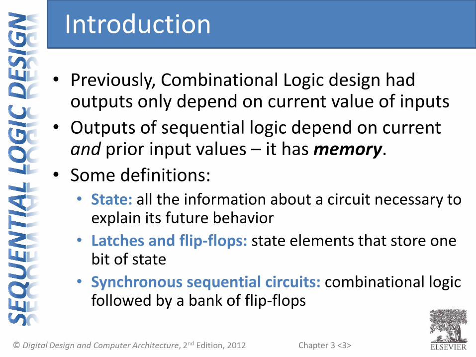
• Previously, Combinational Logic design had outputs only depend on current value of inputs
• Outputs of sequential logic depend on current and prior input values – it has memory.
• Some definitions: • State: all the information about a circuit necessary to
explain its future behavior
• Latches and flip-flops: state elements that store one bit of state
• Synchronous sequential circuits: combinational logic followed by a bank of flip-flops
Introduction

Chapter 3 <4>
• Give sequence to events (i.e. a notion of time)
• Have memory (short-term)
• Use feedback from output to input to store
information
• Need to “remember” past output
Sequential Circuits

Chapter 3 <5>
• The state of a circuit influences its future
behavior
• State elements store state
• Bistable circuit
• SR Latch
• D Latch
• D Flip-flop
State Elements

Chapter 3 <6>
QQQ
Q
I1
I2
I2 I1
• Fundamental building block of other state
elements
• Two outputs: Q, Q (state)
• No inputs
Bistable Circuit
0 1 0 1 0 1
Redrawn circuit to emphasize symmetry

Chapter 3 <7>
Q
Q
I1
I2
0
1
1
0
• Consider the two possible cases:
• Q = 0:
then Q = 1, Q = 0 (consistent)
Bistable Circuit Analysis

Chapter 3 <8>
Q
Q
I1
I2
0
1
1
0
Q
Q
I1
I2
1
0
0
1
• Consider the two possible cases:
• Q = 0:
then Q = 1, Q = 0 (consistent)
• Q = 1:
then Q = 0, Q = 1 (consistent)
• Stores 1 bit of state in the state variable, Q (or Q)
• But there are no inputs to control the state
Bistable Circuit Analysis

Chapter 3 <9>
R
S
Q
Q
N1
N2
• SR Latch
• S – set Q=1
• R – reset Q=0
SR (Set/Reset) Latch

Chapter 3 <10>
R
S
Q
Q
N1
N2
• SR Latch
• Consider the four possible cases:
• S = 1, R = 0
• S = 0, R = 1
• S = 0, R = 0
• S = 1, R = 1
SR (Set/Reset) Latch

Chapter 3 <11>
• S = 1, R = 0:
then Q = 1 and Q = 0
SR Latch Analysis
R
S
Q
Q
N1
N2
0
1
1
00
0

Chapter 3 <12>
• S = 1, R = 0:
then Q = 1 and Q = 0
SR Latch Analysis
R
S
Q
Q
N1
N2
0
1
1
00
0
Chapter 3 <13>
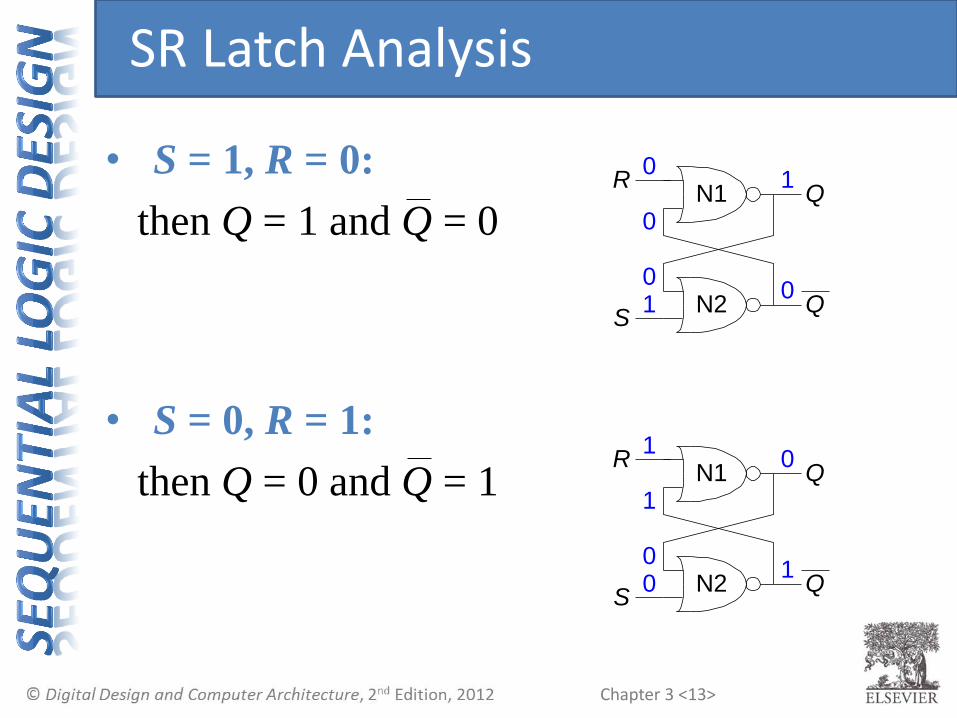
• S = 1, R = 0:
then Q = 1 and Q = 0
• S = 0, R = 1:
then Q = 0 and Q = 1
SR Latch Analysis
R
S
Q
Q
N1
N2
0
1
1
00
0
R
S
Q
Q
N1
N2
1
0
0
10
1

Chapter 3 <14>
• S = 1, R = 0:
then Q = 1 and Q = 0
Set the output
• S = 0, R = 1:
then Q = 0 and Q = 1
Reset the output
SR Latch Analysis
R
S
Q
Q
N1
N2
0
1
1
00
0
R
S
Q
Q
N1
N2
1
0
0
10
1
Chapter 3 <15>
R
S
Q
Q
N1
N2
0
0
R
S
Q
Q
N1
N2
0
0
0
Qprev
= 0 Qprev
= 1
1
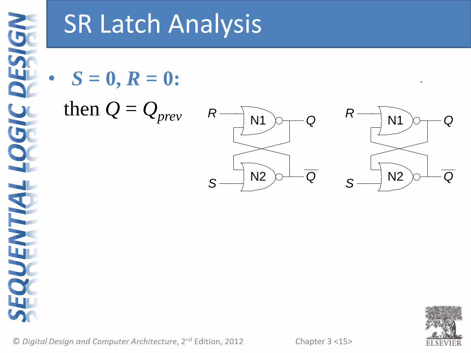
• S = 0, R = 0:
then Q = Qprev
SR Latch Analysis

Chapter 3 <16>
R
S
Q
Q
N1
N2
0
0
R
S
Q
Q
N1
N2
0
0
0
Qprev
= 0 Qprev
= 1
1
• S = 0, R = 0:
then Q = Qprev
SR Latch Analysis

Chapter 3 <17>
R
S
Q
Q
N1
N2
0
0
R
S
Q
Q
N1
N2
0
0
0
Qprev
= 0 Qprev
= 1
1
• S = 0, R = 0:
then Q = Qprev
• S = 1, R = 1:
then Q = 0, Q = 0
SR Latch Analysis
R
S
Q
Q
N1
N2
1
1
0
00
0

Chapter 3 <18>
R
S
Q
Q
N1
N2
0
0
R
S
Q
Q
N1
N2
0
0
0
Qprev
= 0 Qprev
= 1
1
• S = 0, R = 0:
then Q = Qprev
• S = 1, R = 1:
then Q = 0, Q = 0
SR Latch Analysis
R
S
Q
Q
N1
N2
1
1
0
00
0

Chapter 3 <19>
R
S
Q
Q
N1
N2
0
0
R
S
Q
Q
N1
N2
0
0
0
Qprev
= 0 Qprev
= 1• S = 0, R = 0:
then Q = Qprev
Memory!
• S = 1, R = 1:
then Q = 0, Q = 0
Invalid State
Q ≠ NOT Q
SR Latch Analysis
R
S
Q
Q
N1
N2
1
1
0
00
0

Chapter 3 <20>
S
R Q
Q
SR Latch
Symbol
• SR stands for Set/Reset Latch
– Stores one bit of state (Q)
• Control what value is being stored with S, R
inputs
• Set: Make the output 1
(S = 1, R = 0, Q = 1)
• Reset: Make the output 0
(S = 0, R = 1, Q = 0)
• Must do something to avoid
invalid state (when S = R = 1)
SR Latch Symbol

Chapter 3 <21>
D Latch
Symbol
CLK
D Q
Q
• Two inputs: CLK, D
• CLK: controls when the output changes
• D (the data input): controls what the output changes to
• Function
• When CLK = 1,
D passes through to Q (transparent)
• When CLK = 0,
Q holds its previous value (opaque)
• Avoids invalid case when
Q ≠ NOT Q
D Latch

Chapter 3 <22>
S
R Q
Q
Q
QD
CLKD
R
S
CLK
D Q
Q
S R Q QCLK D
0 X
1 0
1 1
D
D Latch Internal Circuit

Chapter 3 <23>
S
R Q
Q
Q
QD
CLKD
R
S
CLK
D Q
Q
S R Q
0 0 Qprev
0 1 0
1 0 1
Q
1
0
CLK D
0 X
1 0
1 1
D
X
1
0
Qprev
D Latch Internal Circuit

Chapter 3 <24>
D Flip-Flop
Symbols
D Q
Q
• Inputs: CLK, D
• Function
– Samples D on rising edge of CLK
• When CLK rises from 0 to 1, D
passes through to Q
• Otherwise, Q holds its previous
value
– Q changes only on rising edge of
CLK
• Called edge-triggered
• Activated on the clock edge
D Flip-Flop

Chapter 3 <25>
CLK
D Q
Q
CLK
D Q
Q
Q
Q
DN1
CLK
L1 L2
• Two back-to-back latches (L1 and L2) controlled by
complementary clocks
• When CLK = 0
• L1 is transparent
• L2 is opaque
– D passes through to N1
D Flip-Flop Internal Circuit

Chapter 3 <26>
CLK
D Q
Q
CLK
D Q
Q
Q
Q
DN1
CLK
L1 L2
• Two back-to-back latches (L1 and L2) controlled by
complementary clocks
• When CLK = 0
– L1 is transparent
– L2 is opaque
– D passes through to N1
• When CLK = 1
– L2 is transparent
– L1 is opaque
– N1 passes through to Q
D Flip-Flop Internal Circuit

Chapter 3 <27>
CLK
D Q
Q
CLK
D Q
Q
Q
Q
DN1
CLK
L1 L2
• Two back-to-back latches (L1 and L2) controlled by
complementary clocks
• When CLK = 0
– L1 is transparent
– L2 is opaque
– D passes through to N1
• When CLK = 1
– L2 is transparent
– L1 is opaque
– N1 passes through to Q
• Thus, on the edge of the clock (when CLK rises from 0 1)
– D passes through to Q
D Flip-Flop Internal Circuit

Chapter 3 <28>
CLK
D Q
Q
D Q
Q
CLK
D
Q (latch)
Q (flop)
D Latch vs. D Flip-Flop

Chapter 3 <29>
CLK
D
Q (latch)
Q (flop)
D Latch vs. D Flip-Flop
CLK
D Q
Q
D Q
Q

Chapter 3 <30>
Review
S
R Q
Q
SR Latch
Symbol
CLK
D Q
Q
D Q
Q
SR Latch D Latch D Flip-flop
S = 1, R = 0: Q = 1
S = 0, R= 1: Q = 0 CLK = 1: Q = D
CLK = 0: Q = Qprev
CLK = 0→1: Q = D
Otherwise: Q = Qprev

Chapter 3 <31>
CLK
D Q
D Q
D Q
D Q
D0
D1
D2
D3
Q0
Q1
Q2
Q3
D3:0
4 4
CLK
Q3:0
Registers

Chapter 3 <32>
Internal
Circuit
D Q
CLKEN
DQ
0
1D Q
EN
Symbol
• Inputs: CLK, D, EN – The enable input (EN) controls when new data (D) is stored
• Function • EN = 1: D passes through to Q on the clock edge
• EN = 0: the flip-flop retains its previous state
Enabled Flip-Flops

Chapter 3 <33>
Internal
Circuit
D Q
CLKEN
DQ
0
1D Q
EN
Symbol
• Inputs: CLK, D, EN – The enable input (EN) controls when new data (D) is stored
• Function • EN = 1: D passes through to Q on the clock edge
• EN = 0: the flip-flop retains its previous state
Enabled Flip-Flops

Chapter 3 <34>
Symbols
D Q
Resetr
• Inputs: CLK, D, Reset
• Function:
• Reset = 1: Q is forced to 0
• Reset = 0: flip-flop behaves as ordinary D flip-flop
Resettable Flip-Flops

Chapter 3 <35>
• Two types:
– Synchronous: resets at the clock edge only
– Asynchronous: resets immediately when Reset = 1
• Asynchronously resettable flip-flop requires
changing the internal circuitry of the flip-flop
• Synchronously resettable flip-flop?
Resettable Flip-Flops

Chapter 3 <36>
• Two types:
– Synchronous: resets at the clock edge only
– Asynchronous: resets immediately when Reset = 1
• Asynchronously resettable flip-flop requires
changing the internal circuitry of the flip-flop
• Synchronously resettable flip-flop?
Resettable Flip-Flops
Internal
Circuit
D Q
CLK
DQ
Reset

Chapter 3 <37>
Symbols
D Q
Sets
• Inputs: CLK, D, Set
• Function:
• Set = 1: Q is set to 1
• Set = 0: the flip-flop behaves as ordinary D flip-
flop
Settable Flip-Flops

Chapter 3 <38>
• Registers inserted between combinational
logic
• Registers contain state of the system
• State changes at clock edge: system
synchronized to the clock
Synchronous Sequential Logic Design

Chapter 3 <39>
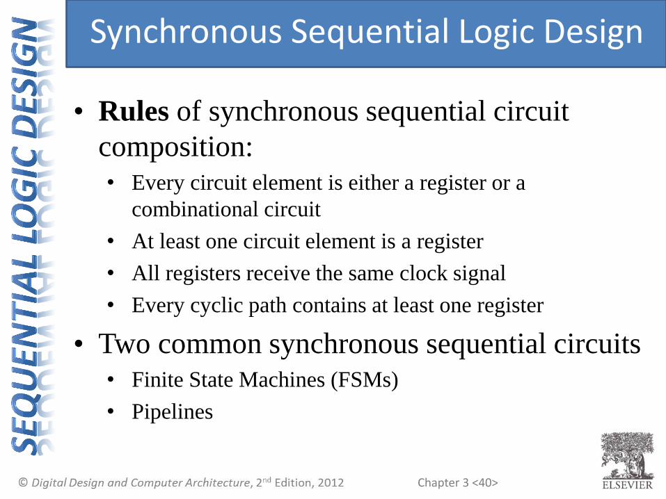
• Rules of synchronous sequential circuit
composition: • Every circuit element is either a register or a
combinational circuit
• At least one circuit element is a register
• All registers receive the same clock signal
• Every cyclic path contains at least one register
Synchronous Sequential Logic Design
Chapter 3 <40>
• Rules of synchronous sequential circuit
composition: • Every circuit element is either a register or a
combinational circuit
• At least one circuit element is a register
• All registers receive the same clock signal
• Every cyclic path contains at least one register
• Two common synchronous sequential circuits • Finite State Machines (FSMs)
• Pipelines
Synchronous Sequential Logic Design