c:/documents and settings/agrawvd/my …
TRANSCRIPT
Built-in Self-Test and Calibration of Mixed-signal Devices
by
Wei Jiang
A dissertation submitted to the Graduate Faculty ofAuburn University
in partial fulfillment of therequirements for the Degree of
Doctor of Philosophy
Auburn, AlabamaMay 9, 2011
Keywords: DFT, BIST, mixed-signal, SoC
Copyright 2011 by Wei Jiang
Approved by
Vishwani D. Agrawal, Chair, James J. Danaher Professor of Electrical and ComputerEngineering
Victor P. Nelson, Professor of Electrical and Computer EngineeringFa F. Dai, Professor of Electrical and Computer Engineering
Adit D. Singh, Professor of Electrical and Computer Engineering
Abstract
Wide adoption of deep sub-micron and nanoscale technologies in the modern semi-
conductor industry is resulted in very large complex mixed-signal devices. It has then be-
come more difficult to estimate and control device parameters, which are now increasingly
vulnerable to fabrication process variations. Conventional design-for-test (DFT) methods
have been already well studied for digital circuitry to ensure verification of its functionality
and fault coverage. Built-in self-test (BIST) approaches have been developed for design
automation of digital ICs. However, such DFT techniques cannot be applied to analog and
mixed-signal circuits directly. Therefore, new techniques must be employed to detect faults
in analog components and to provide certain level of calibration capability to dynamically
adjust the parameters of an analog device for better yield ofchips. The most important ana-
log devices in a mixed-signal system-on-chip (SoC) are analog-to-digital converter (ADC)
and digital-to-analog converter (DAC). Such converters transfer data between digital and
analog circuits and convert analog signals to digital bits or vice versa. In this research,
novel digital signal processor (DSP)-based post-fabrication process-independent BIST ap-
proaches and variation tolerant design technique for ADC and DAC are studied. We use a
sigma-delta modulation technique for measurement and a polynomial fitting algorithm for
device calibration. In the proposed technique, a digital signal processor is programmed and
used as test pattern generator (TPG), output response analyzer (ORA) and test control unit.
The polynomial fitting algorithm characterizes the nonlinearity errors and the polynomial
is used to generate compensating signals to reduce nonlinearity errors to±0.5LSB. This
ii

technique can be applied to other digitally-controllable mixed-signal devices and a general
test-characterization-calibration approach modeled after this work can be developed to de-
tect, measure, and compensate nonlinearity errors caused by device parameter deviations.
iii

Acknowledgments
I would like to thank my supervisor, Dr. Vishwani Agrawal, James J. Danaher Profes-
sor of Electrical and Computer Engineering, for his great help with my courses, research
and projects. His patience and kindness always encouraged me to overcome difficulties
during tough times. I appreciate his knowledge and experience in both academic and in-
dustrial fields, and his valuable suggestions and feedback which greatly contributed to this
dissertation. I would like to thank members of my committee,Dr. Victor P. Nelson, Dr. Fa
F. Dai and Dr. Adit. D. Singh for their assistance and help during my research.
I am grateful to my wife, Lan Luo, for her support and care thatgive me strength
through my life. I thank my parents for their love and courage.
I recognize that this research was supported in parts by the National Science Founda-
tion Grant CNS-0708962 and by the Wireless Engineering Research and Education Center
(WEREC) at Auburn University. I would like to thank Broadcom Corporation for the help
and resources they provided during the final year of this research.
iv
Table of Contents
Abstract . . . . . . . . . . . . . . . . . . . . . . . . . . . . . . . . . . . . . . . . . ii
Acknowledgments . . . . . . . . . . . . . . . . . . . . . . . . . . . . . . . . . . . .iv
List of Figures . . . . . . . . . . . . . . . . . . . . . . . . . . . . . . . . . . . . . .viii
List of Tables . . . . . . . . . . . . . . . . . . . . . . . . . . . . . . . . . . . . . . xi
1 Introduction . . . . . . . . . . . . . . . . . . . . . . . . . . . . . . . . . . . . 1
1.1 Overview . . . . . . . . . . . . . . . . . . . . . . . . . . . . . . . . . . . 2
1.1.1 Digital Testing Techniques . . . . . . . . . . . . . . . . . . . . . .3
1.1.2 Mixed-Signal Devices . . . . . . . . . . . . . . . . . . . . . . . . 6
1.1.3 ADC and DAC . . . . . . . . . . . . . . . . . . . . . . . . . . . . 9
1.1.4 Process Variation . . . . . . . . . . . . . . . . . . . . . . . . . . . 10
1.2 Motivation and Objectives . . . . . . . . . . . . . . . . . . . . . . . . .. 13
1.3 Contributions . . . . . . . . . . . . . . . . . . . . . . . . . . . . . . . . . 16
2 Background . . . . . . . . . . . . . . . . . . . . . . . . . . . . . . . . . . . . 20
2.1 Analysis and Test of ADC and DAC . . . . . . . . . . . . . . . . . . . . . 20
2.1.1 Resolution and Non-Linearity Errors . . . . . . . . . . . . . . .. . 21
2.1.2 Noise . . . . . . . . . . . . . . . . . . . . . . . . . . . . . . . . . 26
2.1.3 Signal-to-Noise Ratio . . . . . . . . . . . . . . . . . . . . . . . . 27
2.1.4 SNDR and ENOB . . . . . . . . . . . . . . . . . . . . . . . . . . 28
2.2 Summary . . . . . . . . . . . . . . . . . . . . . . . . . . . . . . . . . . . 30
3 BIST Architecture for Mixed-Signal Devices . . . . . . . . . . . . .. . . . . 31
v
3.1 Test of Mixed-Signal Devices . . . . . . . . . . . . . . . . . . . . . . .. . 31
3.1.1 ADC/DAC Test Methods . . . . . . . . . . . . . . . . . . . . . . . 31
3.1.2 Available Test Methods . . . . . . . . . . . . . . . . . . . . . . . . 32
3.1.3 Servo-Loop Testing Method . . . . . . . . . . . . . . . . . . . . . 33
3.1.4 Sigma-Delta Testing Method . . . . . . . . . . . . . . . . . . . . . 35
3.1.5 Histogram Testing Method . . . . . . . . . . . . . . . . . . . . . . 36
3.2 Proposed Approaches . . . . . . . . . . . . . . . . . . . . . . . . . . . . . 39
3.3 Testing Steps of BIST Architecture . . . . . . . . . . . . . . . . . . .. . . 40
3.4 Components of BIST Architecture . . . . . . . . . . . . . . . . . . . . . .43
3.4.1 Analog Signal Generator . . . . . . . . . . . . . . . . . . . . . . . 43
3.4.2 Measuring-ADC . . . . . . . . . . . . . . . . . . . . . . . . . . . 47
3.4.3 Dithering-DAC . . . . . . . . . . . . . . . . . . . . . . . . . . . . 50
3.4.4 Digital Test Pattern Generator . . . . . . . . . . . . . . . . . . .. 53
3.5 Testing of On-chip Converters . . . . . . . . . . . . . . . . . . . . . . .. 58
3.5.1 Diagnosis of Testing Components . . . . . . . . . . . . . . . . . . 59
3.5.2 Test of On-Chip ADC . . . . . . . . . . . . . . . . . . . . . . . . 61
3.5.3 Test of On-Chip DAC . . . . . . . . . . . . . . . . . . . . . . . . 66
3.5.4 Calibration of On-Chip ADC/DAC . . . . . . . . . . . . . . . . . 71
3.5.5 Verification of ADC/DAC Test Results . . . . . . . . . . . . . . . 76
3.5.6 Minimal Number of Samples . . . . . . . . . . . . . . . . . . . . . 79
3.5.7 Delay of Polynomial Evaluation . . . . . . . . . . . . . . . . . . .80
3.6 Summary . . . . . . . . . . . . . . . . . . . . . . . . . . . . . . . . . . . 81
4 Sigma-Delta ADC . . . . . . . . . . . . . . . . . . . . . . . . . . . . . . . . . 82
vi
4.1 First-order 1-bit Sigma-Delta Modulation . . . . . . . . . . .. . . . . . . 82
4.1.1 Oversampling and Noise Shaping Techniques . . . . . . . . .. . . 87
4.2 Digital Filter . . . . . . . . . . . . . . . . . . . . . . . . . . . . . . . . . . 90
4.3 Summary . . . . . . . . . . . . . . . . . . . . . . . . . . . . . . . . . . . 92
5 Polynomial Fitting Algorithm . . . . . . . . . . . . . . . . . . . . . . . .. . . 94
5.1 Overview . . . . . . . . . . . . . . . . . . . . . . . . . . . . . . . . . . . 94
5.2 Fitting Algorithm . . . . . . . . . . . . . . . . . . . . . . . . . . . . . . . 94
5.2.1 Linear Fitting . . . . . . . . . . . . . . . . . . . . . . . . . . . . . 96
5.2.2 Second-Order Fitting and Third-Order Fitting . . . . . .. . . . . . 97
5.2.3 Higher-Order Fitting . . . . . . . . . . . . . . . . . . . . . . . . . 99
5.3 Adaptive Fitting . . . . . . . . . . . . . . . . . . . . . . . . . . . . . . . . 100
6 Conclusion . . . . . . . . . . . . . . . . . . . . . . . . . . . . . . . . . . . . 108
6.1 Truncation Error . . . . . . . . . . . . . . . . . . . . . . . . . . . . . . . 108
6.2 Overhead . . . . . . . . . . . . . . . . . . . . . . . . . . . . . . . . . . . 110
6.3 Test Time . . . . . . . . . . . . . . . . . . . . . . . . . . . . . . . . . . . 111
6.4 Summary . . . . . . . . . . . . . . . . . . . . . . . . . . . . . . . . . . . 112
Bibliography . . . . . . . . . . . . . . . . . . . . . . . . . . . . . . . . . . . . . . 113
Appendices . . . . . . . . . . . . . . . . . . . . . . . . . . . . . . . . . . . . . . . 118
A Abbreviations . . . . . . . . . . . . . . . . . . . . . . . . . . . . . . . . . . . 119
B OSR and SNR of Sigma-Delta Modulation . . . . . . . . . . . . . . . . . .. . 121
vii
List of Figures
1.1 World semiconductor sales, 1982-2002 [1]. . . . . . . . . . . .. . . . . . . . 3
1.2 IEEE 1149.1 architecture. . . . . . . . . . . . . . . . . . . . . . . . . .. . . 4
1.3 A typical boundary scan architecture. . . . . . . . . . . . . . . .. . . . . . . 5
1.4 The basic BIST architecture. . . . . . . . . . . . . . . . . . . . . . . . .. . . 6
1.5 A basic analog tester scheme. . . . . . . . . . . . . . . . . . . . . . . .. . . 8
1.6 A typical architecture of mixed-signal system-on-chip(SoC), consisting of
digital circuitry, ADC/DAC, and analog circuitry. . . . . . . . . .. . . . . . . 9
1.7 Different scales of process variation [2]. . . . . . . . . . . .. . . . . . . . . . 11
1.8 Digital BIST with inputs and outputs. . . . . . . . . . . . . . . . . .. . . . . 14
1.9 Techniques of analog test signal using periodical bit-stream and low-pass filter
(LPF) [3]. . . . . . . . . . . . . . . . . . . . . . . . . . . . . . . . . . . . . . 15
2.1 Non-linearity error in ADC. . . . . . . . . . . . . . . . . . . . . . . . . .. . 21
2.2 Non-linearity error in DAC. . . . . . . . . . . . . . . . . . . . . . . . . .. . 22
2.3 Resolution and the least significant bit (LSB) of converters. . . . . . . . . . . . 23
viii
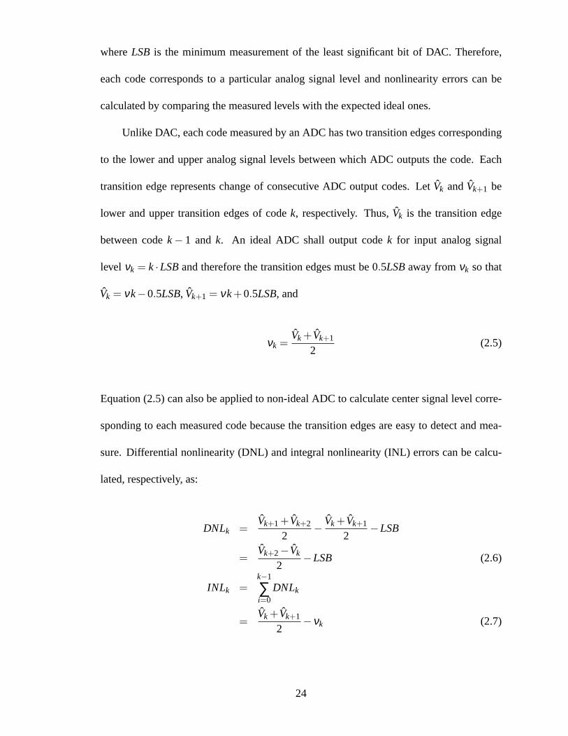
2.4 Transfer function of a quantizer. . . . . . . . . . . . . . . . . . . .. . . . . . 25
2.5 Resolution vs SNR of converters. . . . . . . . . . . . . . . . . . . . . .. . . 29
3.1 Typical servo-loop testing methods for ADC in a mixed-signal system with a
local analog feedback loop [4]. . . . . . . . . . . . . . . . . . . . . . . . .. . 32
3.2 The proposed mixed-signal BIST architecture for testingboth ADC and DAC. . 39
3.3 Diagnosis of testing hardware, including an analog signal generator, a high-
resolution measuring ADC and a low-resolution dithering DAC. . . . . . . . . 41
3.4 Design of ramp testing signal generator [5]. . . . . . . . . . .. . . . . . . . . 45
3.5 Test on-chip DAC by DSP and measuring ADC. . . . . . . . . . . . . . .. . . 48
3.6 DUT calibration by dithering DAC (d-DAC) and best matching polynomial. . . 52
3.7 Schematics of digital test pattern generator (DTPG). . .. . . . . . . . . . . . 54
3.8 Typical analog ramp signals from DTPG patterns. . . . . . . .. . . . . . . . . 56
3.9 Diagnosis of analog signal generator and measuring ADC. .. . . . . . . . . . 59
3.10 Diagnosis of dithering DAC and measuring ADC. . . . . . . . . .. . . . . . . 60
3.11 The proposed ADC BIST architecture. . . . . . . . . . . . . . . . . .. . . . . 62
3.12 Test circuitry of DAC. . . . . . . . . . . . . . . . . . . . . . . . . . . . . .. 67
3.13 INL of simulated 14-bit DAC-under-test. . . . . . . . . . . . . .. . . . . . . 73
ix
3.14 Least mean-square fit third-order polynomial (top) andestimation error (bot-
tom) for DAC-under-test INL data of Figure 3.13. . . . . . . . . . . .. . . . . 74
3.15 INL (top) of simulated 6-bit dithering DAC, and DAC outputs (bottom). . . . . 75
3.16 INL (top) of calibrated 14-bit DAC-under-test using third-order polynomial fit
and 6-bit dithering DAC, and corresponding estimated INL error (bottom). . . . 76
3.17 Proposed digital ADC self-test architecture. . . . . . . .. . . . . . . . . . . . 77
3.18 Test of DAC with loopback connection between DAC outputand ADC/m-
ADC input ports. . . . . . . . . . . . . . . . . . . . . . . . . . . . . . . . . . 77
4.1 Schematic of an typical ADC based on first-order 1-bit Sigma-Delta modula-
tion and its transfer function inz-domain. . . . . . . . . . . . . . . . . . . . . 83
4.2 Oversampling system without noise-shaping feedback. .. . . . . . . . . . . . 87
4.3 Oversampling system with noise-shaping feedback. . . . .. . . . . . . . . . . 89
5.1 Polynomial fitting algorithm of DAC/ADC. . . . . . . . . . . . . . . .. . . . 95
5.2 INL errors of a 14-bit on-chip DAC-under-test. . . . . . . . . .. . . . . . . . 103
5.3 Fitting results from different order polynomials. . . . .. . . . . . . . . . . . . 105
5.4 Correcting signals converted by a 6-bit d-DAC using third-order fitting poly-
nomial. . . . . . . . . . . . . . . . . . . . . . . . . . . . . . . . . . . . . . . 106
5.5 INL errors of 14-bit on-chip DAC corrected using 6-bit d-DAC. . . . . . . . . 107
x
List of Tables
3.1 Third-order polynomial fit for INL of Figure 3.13. . . . . . .. . . . . . . . . . 75
5.1 Zero-order polynomial fit forINL of Figure 5.2. . . . . . . . . . . . . . . . . . 104
5.2 First-order polynomial fit forINL of Figure 5.2. . . . . . . . . . . . . . . . . . 104
5.3 Second-order polynomial fit forINL of Figure 5.2. . . . . . . . . . . . . . . . 104
5.4 Third-order polynomial fit forINL of Figure 5.2. . . . . . . . . . . . . . . . . 104
6.1 Truncation Error for 10-bit DAC. (All unit in LSB) . . . . . . . .. . . . . . . 109
6.2 Truncation Error for 12-bit DAC. (All unit in LSB) . . . . . . . .. . . . . . . 109
6.3 Truncation Error for 16-bit DAC. (All unit in LSB) . . . . . . . .. . . . . . . 109
6.4 Hardware overhead of polynomial evaluation unit (in equivelant NAND gatesand D flip-flops, respectively). . . . . . . . . . . . . . . . . . . . . . . . .. . 110
xi
Chapter 1
Introduction
Digital test technology has been developing for nearly 40 years and has evolved into
hardware and software based testing techniques. In early years, a test bench had to be de-
signed and constructed for each circuit. Later, automatic test equipment (ATE) provided
a general test solution for all digital devices. During the ATE period, the complexity and
density of digital circuits increased dramatically while at the same time better quality and
reliability were required by the market and consumers. ManyVLSI test issues are espe-
cially challenging in high-performance and high-reliability designs. This trend is making
the validation of VLSI circuits more and more difficult. Both external ATE machines,
which are used in the IC production stage, and embedded test solutions, which are required
for chip diagnosis and test are necessary in the design of modern electronic systems. The
need to adopt or establish automated testing standards has been recognized by most manu-
facturing companies as essential for higher yield and lowercost.
However, no such automatic process exists for mixed-signalcircuits where the inter-
face between digital and analog components, in most case, digital-to-analog and analog-to-
digital converters (DAC and ADC), may be impossible to be directly accessed by the test
circuit and equipment.
Often, test circuitry must be embedded to overcome the problem of testing and allow
both digital and analog components in a system to be accessedand tested independently.
Usually such kind of testing techniques involve the use of additional pins, chip area and
1

design time. With the increased complexity of mixed-signalcircuits and reduced access to
internal nodes and paths, proper and efficient testing of such devices is becoming a major
bottleneck during design and testing phases. Additionally, the current tendency to integrate
both analog and digital circuits onto a single die leads to new testing problems, generally
the analog part the root cause of major testing problems. Mixed-signal components, at the
interface between digital and analog parts of a single chip,play a critical role in the overall
performance of the whole chip.
In this thesis, a novel DSP-based post-fabrication processvariation tolerant design
technique for mixed-signal devices is discussed and a general test-characterization-calibration
approach is developed to compensate for parameter deviations in those devices.
1.1 Overview
In recent decades, rapid advances in IC industry have led design functionality and
complexity to unprecedented level motivated by deep sub-micron technology and nanoscale
technology (65nm and beyond).
As the chip feature size keeps shrinking, more components can be integrated onto a
single device. While the performance of such a device has beenimproving, power con-
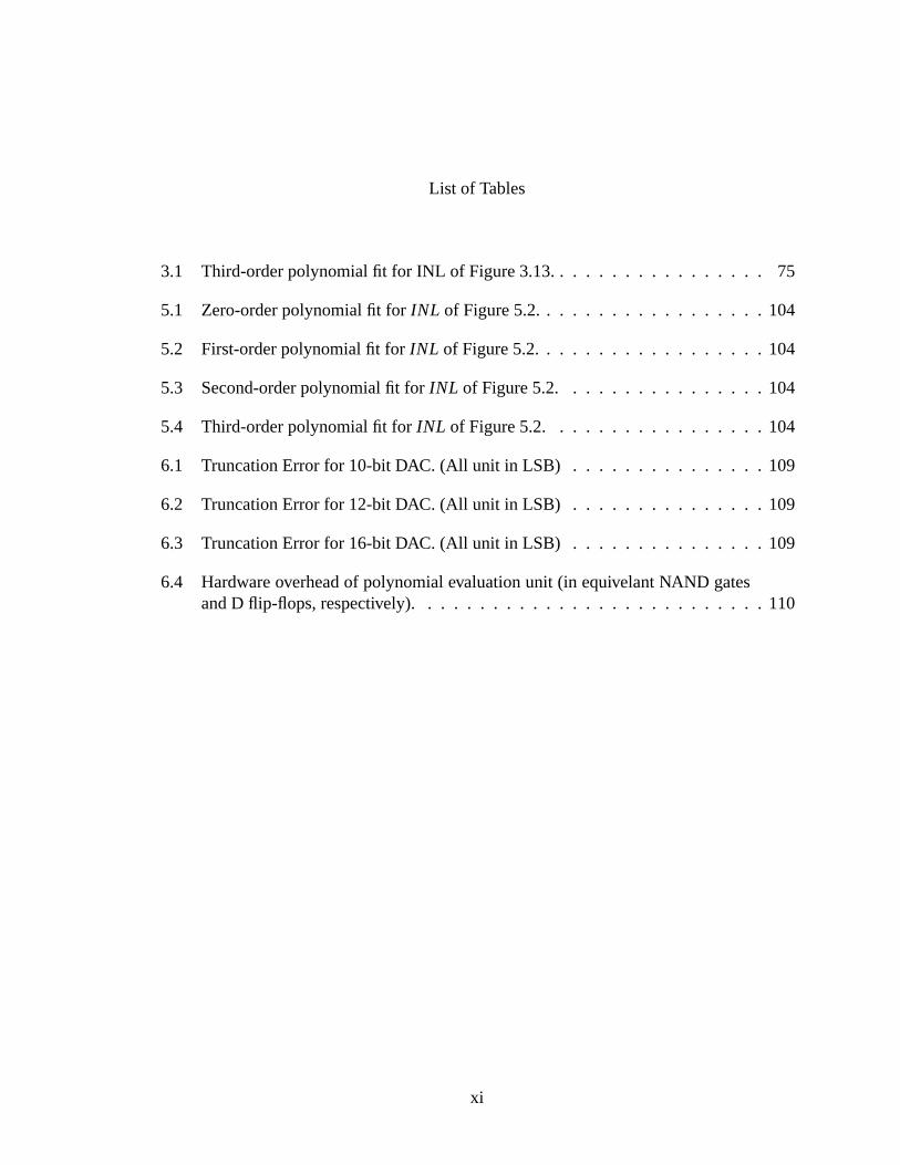
sumption is reducing and manufacturing cost is dropping. Figure 1.1 demonstrates the
rapid growth of IC sales for 20 years between 1982 and 2002.
2
1982 1984 1986 1988 1990 1992 1994 1996 1998 2000 20020
50
100
150
200
250
Year
$ m
illio
ns
Figure 1.1: World semiconductor sales, 1982-2002 [1].
1.1.1 Digital Testing Techniques
Design-for-test (DFT) techniques have been used for digital ICs to achieve such ob-
jectives as test circuit insertion, test pattern generation, fault detection, and fault coverage
analysis.
Purely digital circuits are usually tested using the stuck-at fault model, which consid-
ers all faults in a digital IC as either tied up to logic 1 or down to logic 0. All digital faults
can be categorized into either stuck-at-0 or stuck-at-1 faults and can assume that every
node can have either one of these two possible faults. For anygiven combinational circuit,
3
INTERNAL LOGIC
M IS C E LLA N E O U S R E G IS T E R S
IN S T R U C TIO N R E G IS TE R
B Y P A S S R E G IS TE R
TA P C O N TR O LLE R
M
U
X
IN P U T
P IN S
O U T P U T
P IN S
S IN S O U T
TD I
B oundary
C e lls
TM S
TC K
TD O
B oundary
C e lls
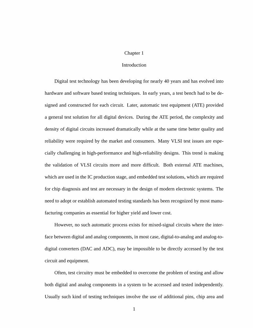
Figure 1.2: IEEE 1149.1 architecture.
a truth-table can be generated by simulation of all possibleinputs. For a certain single-fault
existing in the circuit-under-test (CUT), it is called a detectable fault if a different truth-
table is generated by the simulation of all possible inputs.For a test sequence, the ratio of
detectable faults to all possible faults of a digital circuit is called fault coverage. The input
values that can detect at least one fault are considered testpatterns. Thus, test patterns are
generated to detect faults in a digital device and the testability of the given device can be
measured by fault coverage. A path sensitization techniqueis used to find proper test pat-
terns for any given detectable fault. Finally, fault collapsing techniques are used to remove
many stuck-at faults and to reduce the total number of test patterns.
Over the years, three major methods have been widely adoptedby integrated circuit
(IC) industry to address the digital testing issues: boundary scan, scan chain and BIST.
Boundary scan is a method for testing wire interconnections between individual ICs
of a circuit board as defined by the IEEE Std.1149.1 [6]. A basic IC architecture of IEEE
1149.1 is shown in Figure 1.2. Boundary scan can be used to isolate an IC chip from other
4
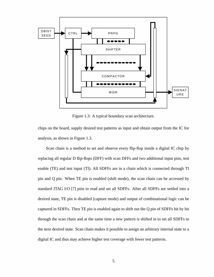
CTRL PRPG
SHIFTER
DBIST SEED
CO M PACTO R
M ISRSIG NAT
URE
Figure 1.3: A typical boundary scan architecture.
chips on the board, supply desired test patterns as input andobtain output from the IC for
analysis, as shown in Figure 1.3.
Scan chain is a method to set and observe every flip-flop insidea digital IC chip by
replacing all regular D flip-flops (DFF) with scan DFFs and twoadditional input pins, test
enable (TE) and test input (TI). All SDFFs are in a chain whichis connected through TI
pin and Q pin. When TE pin is enabled (shift mode), the scan chain can be accessed by
standard JTAG I/O [7] pins to read and set all SDFFs. After allSDFFs are settled into a
desired state, TE pin is disabled (capture mode) and output of combinational logic can be
captured in SDFFs. Then TE pin is enabled again to shift out the Q pin of SDFFs bit by bit
through the scan chain and at the same time a new pattern is shifted in to set all SDFFs to
the next desired state. Scan chain makes it possible to assign an arbitrary internal state to a
digital IC and thus may achieve higher test coverage with fewer test patterns.
5
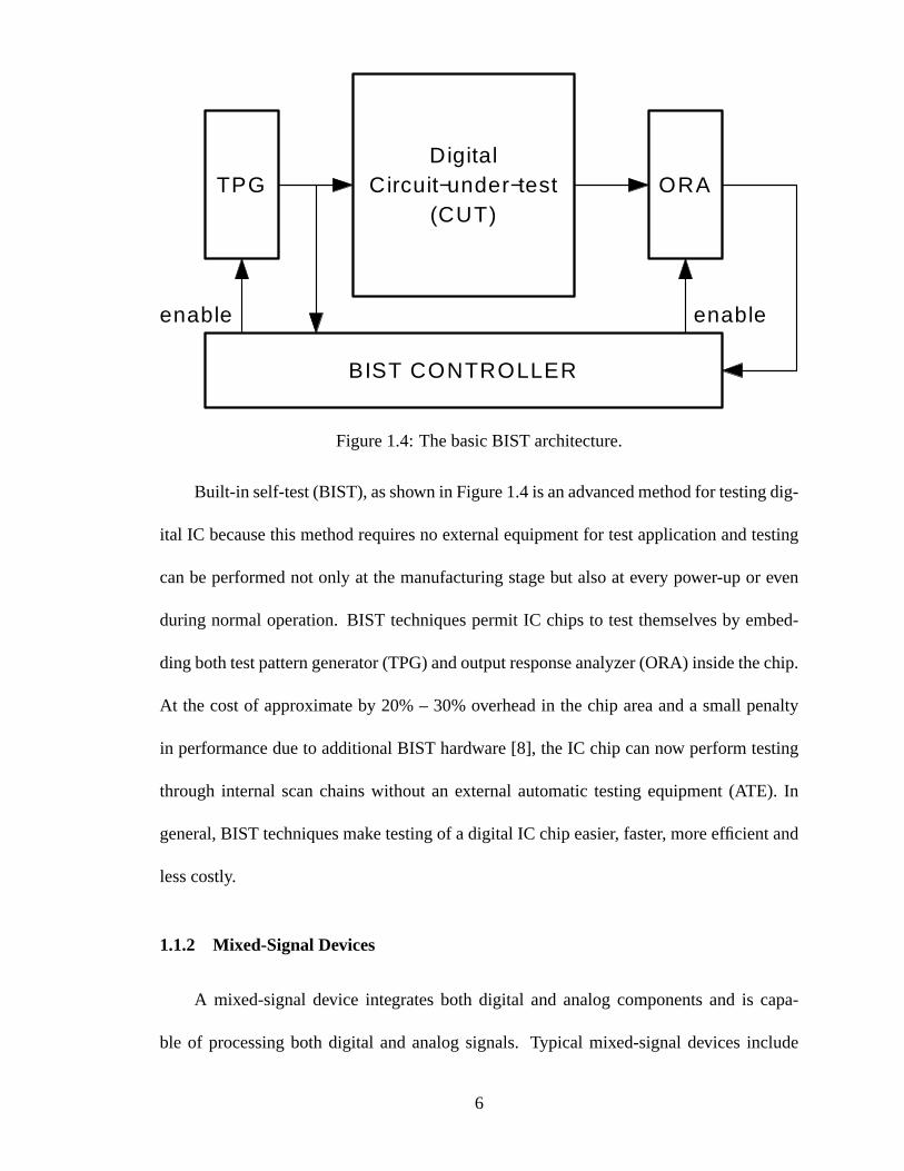
Digital Circuit−under−test
(CUT)
BIST CONTROLLER
TPG ORA
enable enable
Figure 1.4: The basic BIST architecture.
Built-in self-test (BIST), as shown in Figure 1.4 is an advanced method for testing dig-
ital IC because this method requires no external equipment for test application and testing
can be performed not only at the manufacturing stage but alsoat every power-up or even
during normal operation. BIST techniques permit IC chips to test themselves by embed-
ding both test pattern generator (TPG) and output response analyzer (ORA) inside the chip.
At the cost of approximate by 20% – 30% overhead in the chip area and a small penalty
in performance due to additional BIST hardware [8], the IC chip can now perform testing
through internal scan chains without an external automatictesting equipment (ATE). In
general, BIST techniques make testing of a digital IC chip easier, faster, more efficient and
less costly.
1.1.2 Mixed-Signal Devices
A mixed-signal device integrates both digital and analog components and is capa-
ble of processing both digital and analog signals. Typical mixed-signal devices include
6

converters (digital-to-analog and analog-to-digital), amplifiers, transceivers, etc. With the
development of new deep sub-micron CMOS technologies, such mixed-signal devices pro-
vide much more functionality than traditional digital or analog devices and hence, they are
widely deployed in various applications. According to a recent report [9], global shipments
of analog and mixed-signal ICs amounted to $31.7 billion in 2005, increased to $37 bil-
lion in 2006, and may hit $67.8 billion by 2011. The increasing demand for mixed-signal
integrated circuits implementing both digital and analog functions on a single semiconduc-
tor die is pushing for increasing higher levels of integration as the fabrication technology
advances.
However, scaling down of the chip feature size and integration of nanoscale digital
and analog components brings new problems in manufacturingand testing of such mixed-
signal devices. With scaling down of the feature size, device parameter deviations become
a critical factor affecting fault occurrence, die yield, reliability, performance, and eventu-
ally the manufacturing cost. More severe the device parameter deviations become, lower is
die yield and higher the final. The deep sub-micron process makes it possible to build com-
plicated and highly integrated mixed-signal System-on-Chip (SoC) with both digital and
analog components, but also leads to difficulties in the testof such components resulting
in prolonged test time and rising test costs. While the area ofanalog/mixed-signal devices
is important for designers and developers, testing of such devices is becoming a dominant
factor of test costs associated with SoC validation [10]. Asdownscaling in CMOS tech-
nologies continues to 22nm, one of the difficult challenges in the near-term will be to deal
with fluctuations and statistical process variation affecting the sub-11nm gate length MOS-
FET [11]. When the feature size of the mixed-signal devices approaches the physical limits,
7
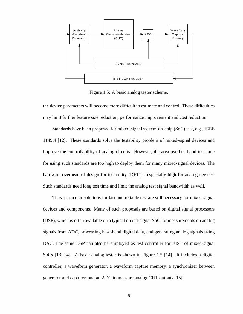
Analog Circuit−under−test
(CUT)
BIST CONTROLLER
SYNCHRONIZER
ADCArbitrary
W aveform Generator
W aveform Capture Memory
Figure 1.5: A basic analog tester scheme.
the device parameters will become more difficult to estimateand control. These difficulties
may limit further feature size reduction, performance improvement and cost reduction.
Standards have been proposed for mixed-signal system-on-chip (SoC) test, e.g., IEEE
1149.4 [12]. These standards solve the testability problemof mixed-signal devices and
improve the controllability of analog circuits. However, the area overhead and test time
for using such standards are too high to deploy them for many mixed-signal devices. The
hardware overhead of design for testability (DFT) is especially high for analog devices.
Such standards need long test time and limit the analog test signal bandwidth as well.
Thus, particular solutions for fast and reliable test are still necessary for mixed-signal
devices and components. Many of such proposals are based on digital signal processors
(DSP), which is often available on a typical mixed-signal SoC for measurements on analog
signals from ADC, processing base-band digital data, and generating analog signals using
DAC. The same DSP can also be employed as test controller for BIST of mixed-signal
SoCs [13, 14]. A basic analog tester is shown in Figure 1.5 [14]. It includes a digital
controller, a waveform generator, a waveform capture memory, a synchronizer between
generator and capturer, and an ADC to measure analog CUT outputs [15].
8
DAC
ADC
ANALOG SYSTEM
ANALOG SYSTEM
Analog System
Input and
Output
DSP
DIGITAL SYSTEM
Digital System
Input and
Output
MIXED SIGNAL
Digital non−linear
error
Analog non−linear
error
Figure 1.6: A typical architecture of mixed-signal system-on-chip (SoC), consisting ofdigital circuitry, ADC/DAC, and analog circuitry.
In this thesis, mixed-signal components, particularly ADC/DAC, are considered and
special DFT techniques to characterize and calibrate such components are studied.
1.1.3 ADC and DAC
Many modern mixed-signal integrated circuit (IC) systems include built-in digital-to-
analog converters (DAC) or analog-to-digital converters (ADC). They are two major com-
ponents of any mixed-signal SoC and their typical test procedure is shown in Figure 1.6.
Because the whole system relies on ADC and DAC to transfer signals between analog
waveforms and digital bit-streams, the overall performance of the mixed-signal SoC de-
pends upon the characteristics of those converters.
The test of high-speed and high-resolution ADC/DAC is a challenging and costly is-
sue for designers and engineers. It has a large impact on fabrication and manufacturing
9
costs. Linearity and resolution are critical measurementsfor DACs and ADCs of a mixed-
signal system-on-chip (SoC). They determine overall performance of the device. With
increasing requirements for high resolution DAC/ADC set by high speed DSP processors
and digital circuitry it becomes more challenging to test the on-chip converters, especially
for system-on-chips (SoC). It also becomes more expensive and difficult to test the high
performance converters using external automated testing equipment (ATE). The digital im-
plementation of analog functions in such mixed-signal devices requires high resolution and
better linearity for on-chip ADC and DAC, especially for communication transmitters and
receivers [16].
1.1.4 Process Variation
The most important factor to affect parameter deviation of mixed-signal devices is
fabrication process variations. Nanoscale technologies have given rise to new problems of
increased parameter variation [11], higher leakage, and time-dependent degradation, all of
which are active research areas.
For deep sub-micron technologies, a combination of physical feature of the process,
dependency on die location, effects of optical proximity and etching and deposition may all
lead to heterogeneous and non-monotonic relationship among the process parameters. The
resulting process variation might be considered completely random effect without detailed
understanding of individual contributions of each factor.
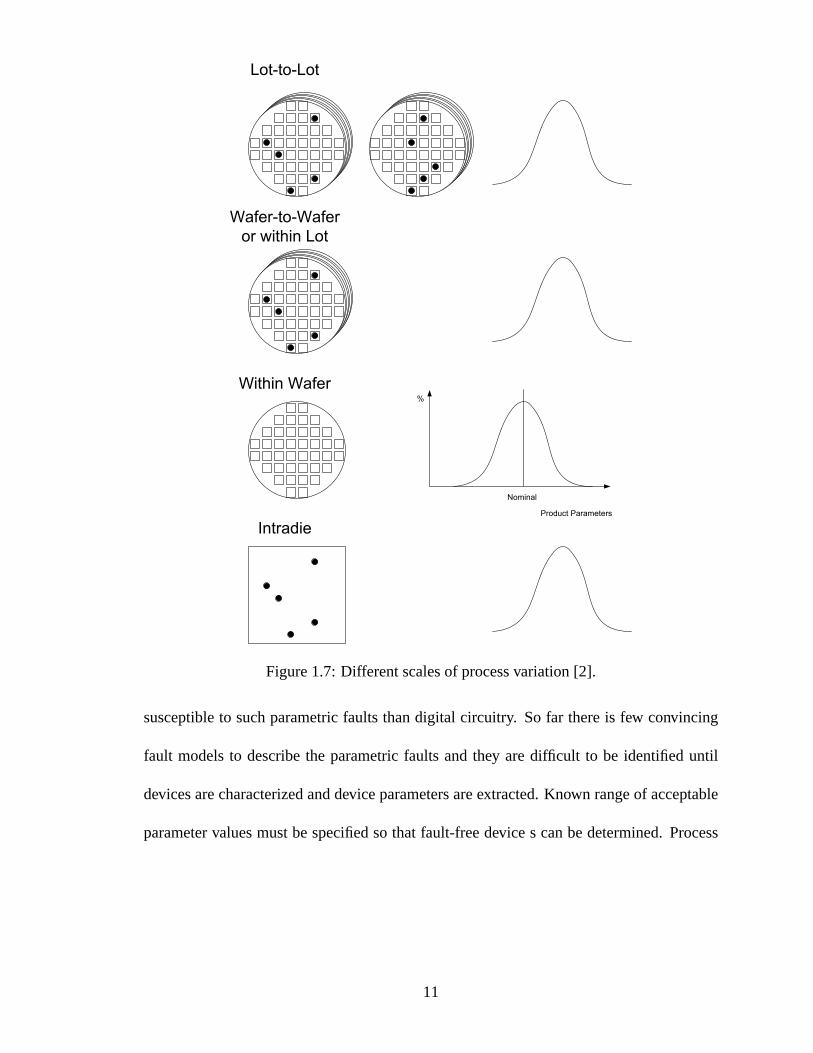
According to Boning and Chung [2], process variation appears at a number of differ-
ent scales, as shown in Figure 1.7 [17]. Parametric faults, or soft faults, means that device
parameters exceed beyond specified tolerance limits and mixed-signal devices are more
10
Product Parameters
Nominal
%
Figure 1.7: Different scales of process variation [2].
susceptible to such parametric faults than digital circuitry. So far there is few convincing
fault models to describe the parametric faults and they are difficult to be identified until
devices are characterized and device parameters are extracted. Known range of acceptable
parameter values must be specified so that fault-free devices can be determined. Process
11
variations may seriously degrade overall mixed-signal system performance when paramet-
ric faults exist. Thus unlike catastrophic faults (hard faults) that need defect-oriented struc-
tural test approach, a specification-oriented functional test shall be employed for test of
parametric faults.
In nanoscale devices, parameters may change (degrade) withtime and with operating
conditions. One such phenomenon that has received attention is thenegative bias temper-
ature instability(NBTI) [18]. The parameter changes will require that any calibration and
compensation procedure should be able to adopt. In this research, we propose a polyno-
mial error fitting type of nonlinearity compensation where the degree of the polynomial is
self-adaptable. Thus, the system can recalibrate the the compensation parameters either the
idle times or the restart of the system.
However, such integration also brings unprecedented challenges to present testing
techniques, especially under nanoscale process. Scaling down feature size to nanoscale
increases difficulties in manufacturing and testing of mixed-signal devices, and further-
more process variation of nanoscale device parameters during fabrication and packaging
becomes a even more critical factors to faults, die yield andeventually unit cost of SoC. As
downscaling in CMOS technologies continues, 22nm is a near-term challenge. Parameter
fluctuations and statistical process variation in sub-11nmgate-length will also continue as
one of the long-term challenges [11].
In a mixed-signal SoC, the challenges of nanoscale technologies [11] more difficult
to deal with. Digital components may require built-in redundancy and reconfiguration, but
analog and mixed-signal components may be correctable through measurement, calibration
and correction schemes [19].
12
1.2 Motivation and Objectives
To deal with the issues in mixed-signal devices mentioned above, especially critical
issues of ADC and DAC as they are the interface between digital and analog circuits inside
the mixed-signal IC chip and therefore the most critical mixed-signal components in such
IC chip, a novel on-chip DSP-based BIST approach for mixed-signal SoC is presented. The
propose BIST approach is digitalized post-fabrication scheme with capability of self-test
and self-calibration for mixed-signal components, in particular ADC and DAC converters.
Digital BIST techniques have been already widely studied andemployed in decades
and a systematic methodology has been developed for testingof digital circuitry. Therefore
it is guaranteed for the digital circuitry used in ADC test tobe fault-free and only ADC-
under-test could be faulty. Discussion of design and implementation of BIST architecture
for digital circuits and DSP is beyond the topic of this thesis, and in the rest of the thesis we
can safely assume the all digital components and circuits for BIST of mixed-signal device
are fault-free. If any fault is found in digital circuitry, the chip under test will be marked as
faulty and BIST for mixed-signal device will not performed after all.
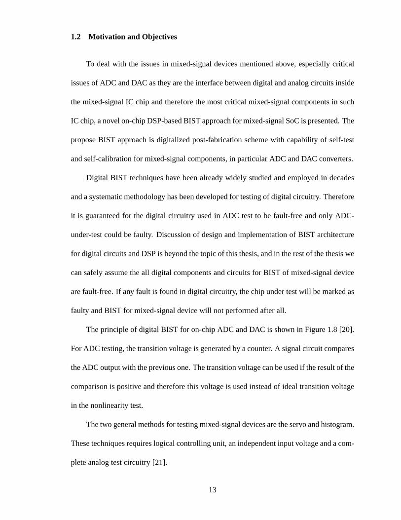
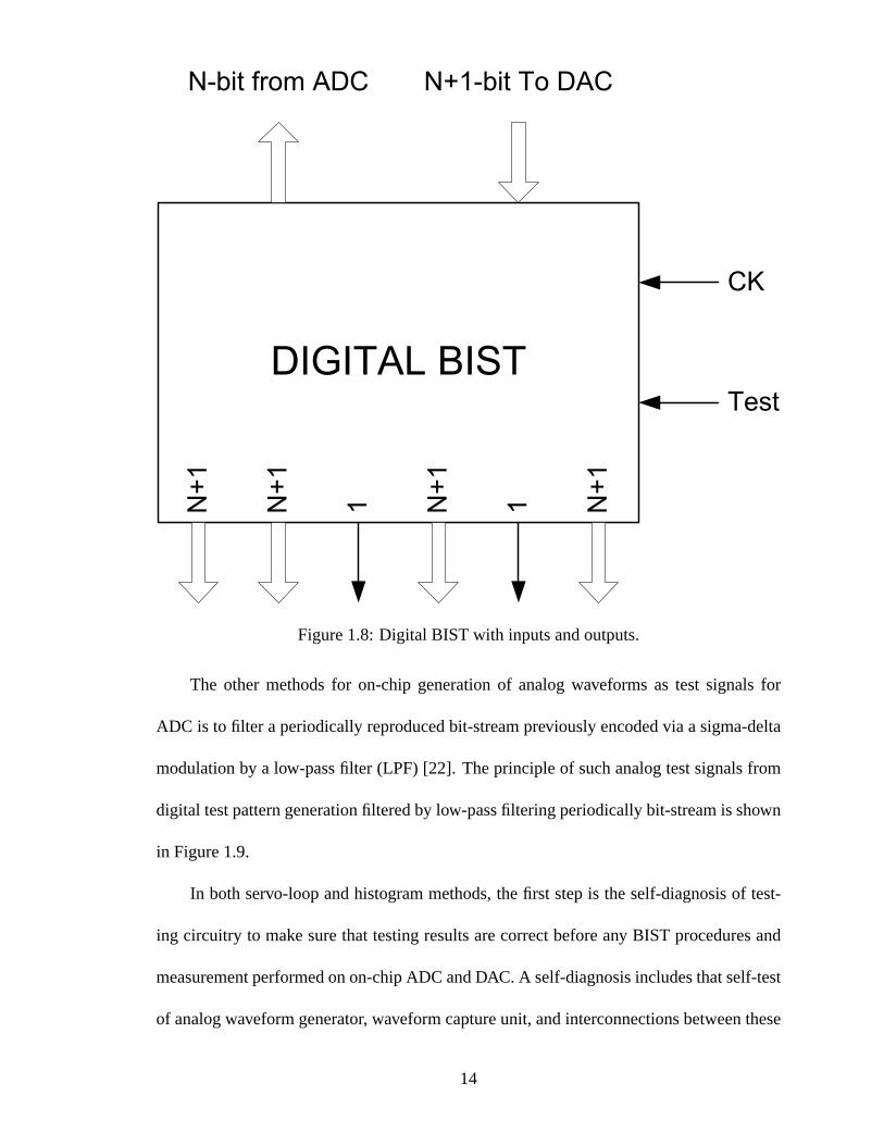
The principle of digital BIST for on-chip ADC and DAC is shown in Figure 1.8 [20].
For ADC testing, the transition voltage is generated by a counter. A signal circuit compares
the ADC output with the previous one. The transition voltagecan be used if the result of the
comparison is positive and therefore this voltage is used instead of ideal transition voltage
in the nonlinearity test.
The two general methods for testing mixed-signal devices are the servo and histogram.
These techniques requires logical controlling unit, an independent input voltage and a com-
plete analog test circuitry [21].
13
N+1
N+1
1 N+1
N+1
1
CK
Test
N-bit from ADC N+1-bit To DAC
Figure 1.8: Digital BIST with inputs and outputs.
The other methods for on-chip generation of analog waveforms as test signals for
ADC is to filter a periodically reproduced bit-stream previously encoded via a sigma-delta
modulation by a low-pass filter (LPF) [22]. The principle of such analog test signals from
digital test pattern generation filtered by low-pass filtering periodically bit-stream is shown
in Figure 1.9.
In both servo-loop and histogram methods, the first step is the self-diagnosis of test-
ing circuitry to make sure that testing results are correct before any BIST procedures and
measurement performed on on-chip ADC and DAC. A self-diagnosis includes that self-test
of analog waveform generator, waveform capture unit, and interconnections between these
14
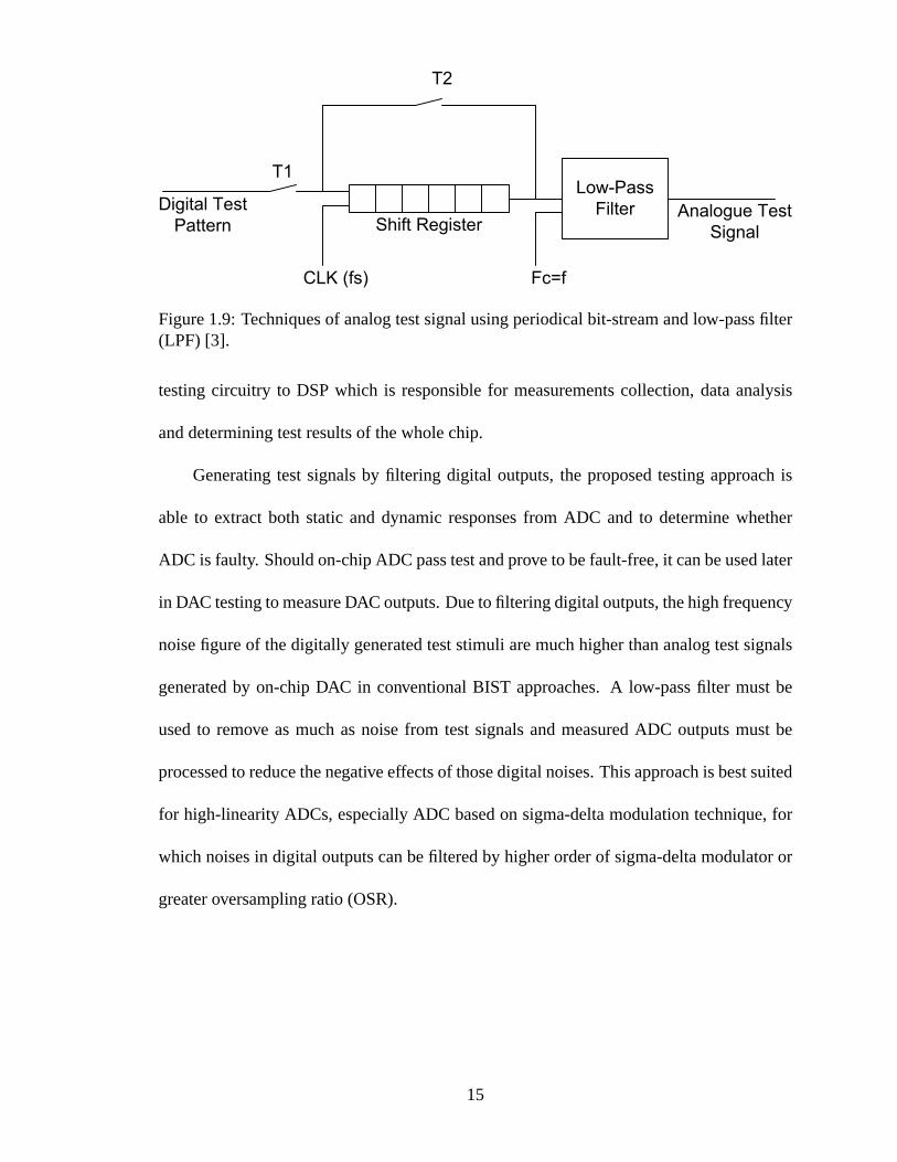
Shift RegisterDigital Test
Pattern
CLK (fs)
T1Low-Pass
Filter
T2
Fc=f
Analogue Test
Signal
Figure 1.9: Techniques of analog test signal using periodical bit-stream and low-pass filter(LPF) [3].
testing circuitry to DSP which is responsible for measurements collection, data analysis
and determining test results of the whole chip.
Generating test signals by filtering digital outputs, the proposed testing approach is
able to extract both static and dynamic responses from ADC and to determine whether
ADC is faulty. Should on-chip ADC pass test and prove to be fault-free, it can be used later
in DAC testing to measure DAC outputs. Due to filtering digital outputs, the high frequency
noise figure of the digitally generated test stimuli are muchhigher than analog test signals
generated by on-chip DAC in conventional BIST approaches. A low-pass filter must be
used to remove as much as noise from test signals and measuredADC outputs must be
processed to reduce the negative effects of those digital noises. This approach is best suited
for high-linearity ADCs, especially ADC based on sigma-delta modulation technique, for
which noises in digital outputs can be filtered by higher order of sigma-delta modulator or
greater oversampling ratio (OSR).
15
1.3 Contributions
Chapter 1 gives an overview of methods for testing mixed-signdevices, especially
for ADC and DAC converters which are the most important mixed-signal components in
such devices. ADC and DAC are the interface between digital and analog circuits and their
characteristics determine the overall performance of a mixed-signal SoC.
Chapter 2 will give necessary background information on the details of the charac-
teristics for ADC/DAC and other mixed-signal devices. The measurement and analysis of
such converters are presented with different factors, including noise, SNR, gain, offset, har-
monic distortion and nonlinearity errors. Among these characteristics, nonlinearity errors
are the major issue for testing of ADC/DAC since nonlinearities of a give ADC or DAC
are the direct results of the process variation and the greatly affected by different factors.
Nonlinearity errors determine the accuracy of conversion from digital vectors to analog
signals (DAC) or vice versa (ADC). Chapter 2 also shows the differences between static
and dynamic test methods. These two methods require different testing methodology and
different designs for TPG and ORA.
In Chapter 3, the details of the proposed testing architectures for mixed-signal devices
are proposed. The major components of testing architectures are designed and analyzed, in-
cluding measuring ADC, dithering DAC, and ramp/sinusoid testing signal generator. Mea-
suring ADC is used for output measurement of on-chip DAC, which generate analog sig-
nals from digital patterns given by DSP. Usually the digitalpatterns are ramp vectors for
static test of DAC to obtain nonlinearity and other characteristic. Ramp signal generator is
used for analog testing signal generation to test on-chip ADC. Ramp signals can be linear,
16
triangle, or saw-tooth signals, all of which is suitable forstatic test of ADC. Sinusoid wave-
forms may also be used for dynamic test of ADC which requires low-frequency sine/cosine
signals.
DSP plays the core role in the testing procedures because digital pattern generation,
measurement analysis, device parameter extraction, device characterization and calibration
are all programmed with the embedded DSP. DSP is also responsible for self-diagnosis of
all testing circuitry since only digital circuits are guaranteed to be fault-free before any test
of mixed-signal circuitry can be performed. DSP can also monitor the status of mixed-
signal device during normal operation by performing characterization of ADC/DAC and
other analog circuits when DSP is idle from other tasks. If drastic change of calculated pa-
rameters of ADC/ADC is detected by DSP, a new calibration procedure can be executed to
re-calibrate the ADC/DAC to ensure the performance of mixed-signal device. This contin-
uous detection and calibration can be programmed as a time-based routine that periodically
executed to keep ADC/DAC calibrated.
In Chapter 4, Sigma-Delta modulation and measuring ADC are discussed. The benefit
of Sigma-Delta modulation is the high-linearity and accuracy achieved by using oversam-
pling and noise-shaping techniques. Oversampling technique distributes in-band quantiza-
tion noise into a much wider frequency range and noise-shaping technique further moves
in-band noise to higher-frequency. Combination of these twotechniques pushes much of
the quantization noise out-of-band into the higher frequency which can be easily removed
through a low-pass filter. The resolution of Sigma-Delta ADCis determined by the over-
sampling ratio, the order of feedback loops and the number ofeffective bits of quantizer
(usually a simple DAC), and the ADC in feedback loop. AlthoughSigma-Delta ADC is
17
considerably slower than any other type of ADC, the proposed mixed-signal BIST archi-
tecture will not take big impact since the Sigma-Delta ADC isonly activated during BIST
phase before any normal operation is executed. Thus the slowconversion rate of Sigma-
Delta ADC will not slow down the normal operation of the mixed-signal devices.
Chapter 5 gives details of a polynomial fitting algorithm proposed by Sunter and
Nagi [23]. An implementation of that algorithm was presented by Royet al. [24]. Poly-
nomial fitting algorithms are used for both characterization of on-chip ADC and DAC, and
the coefficients of the polynomial determined by the algorithm are used for calibration of
on-chip DAC. A low-resolution dithering DAC is driven by a polynomial computation unit
to generate calibrating signals for each input digital codeof on-chip DAC. Thus the final
output of calibrated DAC is the combination of both outputs from on-chip DAC and dither-
ing DAC which removes detected nonlinearity errors from on-chip DAC outputs. Various
orders of polynomial fitting are discussed, from linear, third-order or even higher order fit-
ting algorithms. An adaptive determination of a proper order of the polynomial fitting is
proposed for various applications and situations. A lower order fitting algorithm is simpler
to design and implement with less overhead in terms of the chip size. A higher order fitting
algorithm gives better fitting for nonlinearities of DAC so that higher-linearity and more
accuracy may be achieved at the cost of more overhead and performance penalty. In most
cases, third-order polynomial fitting appears best for mostapplications for balancing the
design complexity and calibration accuracy.
In Chapter 6, details of fault detection and calibration process are presented. A fault
in a mixed-signal circuit is different from that of a digitalcircuit and therefore the stuck-at
18

fault model widely used in digital testing techniques cannot be used in testing of mixed-
signal devices. Fault models for ADC/DAC and further genericmixed-signal circuits are
presented. In fact, the faults in mixed-signal circuits arenot the simple on-off types as in
digital circuits. The faults in a mixed-signal circuit are determined by the allowable range of
each parameter which is characterized during mixed-signaltesting and measuring phases.
If any parameter exceeds its allowable range (either high-side watermark or low-side one),
the mixed-signal circuits will be considered faulty. A mixed-signal circuit is fault-free only
if all obtained parameters are within their respective ranges. Therefore, calibration of a
given mixed-signal circuit, particularly ADC/DAC, uses additional hardware to alter output
signals of the ADC/DAC to make all obtained parameters withinthe allowable ranges.
Portions of the work reported in this dissertation have appeared in three recent pa-
pers [25, 26, 27].
19
Chapter 2
Background
Many analog testing methods tend to be specification-oriented as opposed to defect-
oriented approaches typically used for testing digital circuitry. A defect-oriented approach
applies the fault model to circuits to find out all possible faults existing in the circuit-
under-test (CUT). One of such widely employed approaches is the stuck-at fault model,
which assume that every net interconnection could be faultyas if stuck at either 1 or 0.
A specification-oriented approach consists of a set of specifications that define the valid
boundary for each measurable characteristic of CUT. When a certain characteristic value
exceeds the defined limited, it will be considered as a fault.This difference partially comes
from the fact that analog circuitry processes analog signals with a given value range instead
of deterministic 0 or 1 found in digital circuitry. The parameters of analog circuitry are also
affected by component tolerances, environmental variations (e.g., temperature and supply
voltage) and noise.
Testing the analog porting of mixed-signal integrated circuits and systems has been
identified as one the major challenges for the future, and BISThas been identified as a
potential solution to this testing challenge [10, 11].
2.1 Analysis and Test of ADC and DAC
This section gives details on test and measurement of various performance character-
istics of ADC/DAC under test, including noise figure and signal-to-noise ratio (SNR).
20
Analog input
Digital code output
Actual
(νK)
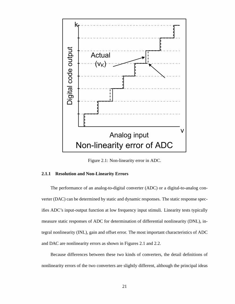
Non-linearity error of ADC
k
ν
Figure 2.1: Non-linearity error in ADC.
2.1.1 Resolution and Non-Linearity Errors
The performance of an analog-to-digital converter (ADC) or adigital-to-analog con-
verter (DAC) can be determined by static and dynamic responses. The static response spec-
ifies ADC’s input-output function at low frequency input stimuli. Linearity tests typically
measure static responses of ADC for determination of differential nonlinearity (DNL), in-
tegral nonlinearity (INL), gain and offset error. The most important characteristics of ADC
and DAC are nonlinearity errors as shown in Figures 2.1 and 2.2.
Because differences between these two kinds of converters, the detail definitions of
nonlinearity errors of the two converters are slightly different, although the principal ideas
21
Ideal
Actual (νK)
Analog output
Digital code input
Non-linearity error of DAC
k
ν
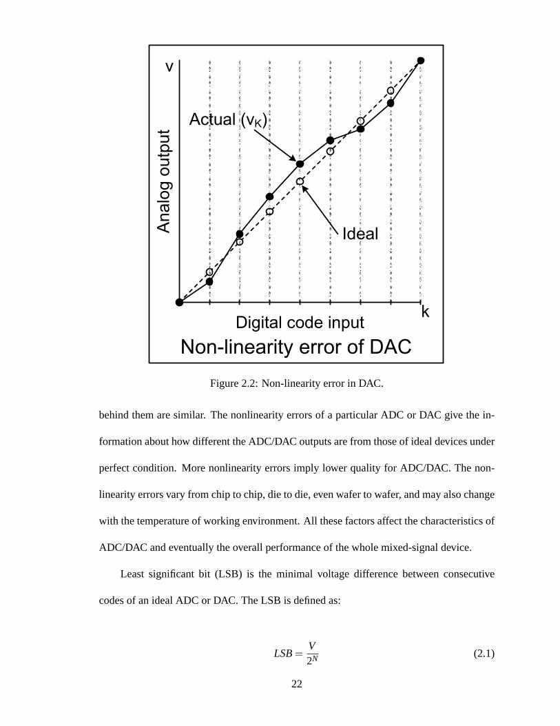
Figure 2.2: Non-linearity error in DAC.
behind them are similar. The nonlinearity errors of a particular ADC or DAC give the in-
formation about how different the ADC/DAC outputs are from those of ideal devices under
perfect condition. More nonlinearity errors imply lower quality for ADC/DAC. The non-
linearity errors vary from chip to chip, die to die, even wafer to wafer, and may also change
with the temperature of working environment. All these factors affect the characteristics of
ADC/DAC and eventually the overall performance of the whole mixed-signal device.
Least significant bit (LSB) is the minimal voltage differencebetween consecutive
codes of an ideal ADC or DAC. The LSB is defined as:
LSB=V2N (2.1)
22
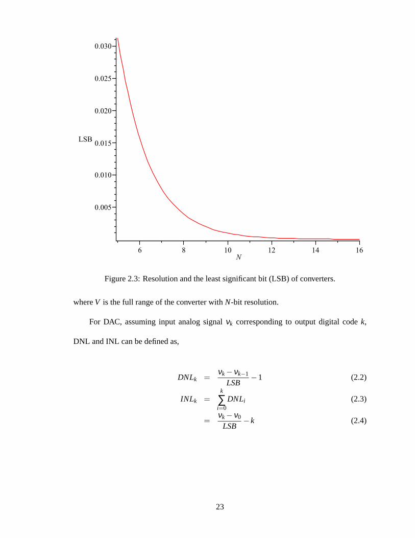
Figure 2.3: Resolution and the least significant bit (LSB) of converters.
whereV is the full range of the converter withN-bit resolution.
For DAC, assuming input analog signalνk corresponding to output digital codek,
DNL and INL can be defined as,
DNLk =νk−νk−1
LSB−1 (2.2)
INLk =k
∑i=0
DNLi (2.3)
=νk−ν0
LSB−k (2.4)
23
whereLSB is the minimum measurement of the least significant bit of DAC.Therefore,
each code corresponds to a particular analog signal level and nonlinearity errors can be
calculated by comparing the measured levels with the expected ideal ones.
Unlike DAC, each code measured by an ADC has two transition edges corresponding
to the lower and upper analog signal levels between which ADCoutputs the code. Each
transition edge represents change of consecutive ADC output codes. LetVk andVk+1 be
lower and upper transition edges of codek, respectively. Thus,Vk is the transition edge
between codek− 1 andk. An ideal ADC shall output codek for input analog signal
level νk = k ·LSBand therefore the transition edges must be 0.5LSBaway fromνk so that
Vk = νk−0.5LSB, Vk+1 = νk+0.5LSB, and
νk =Vk+Vk+1
2(2.5)
Equation (2.5) can also be applied to non-ideal ADC to calculate center signal level corre-
sponding to each measured code because the transition edgesare easy to detect and mea-
sure. Differential nonlinearity (DNL) and integral nonlinearity (INL) errors can be calcu-
lated, respectively, as:
DNLk =Vk+1+Vk+2
2− Vk+Vk+1
2−LSB
=Vk+2−Vk
2−LSB (2.6)
INLk =k−1
∑i=0
DNLk
=Vk+Vk+1
2−νk (2.7)
24
x
y
1
-1
∆/2
-∆/2
3∆/2
-3∆/2
Figure 2.4: Transfer function of a quantizer.
ADC codes 0 and 2N −1 are special as code 0 does not have the lower transition edge
and code 2N −1 does not have an upper edge, so the analog signal level corresponding to
these two codes cannot be calculated by (2.5).
25

2.1.2 Noise
Quantization noise is a major source of nonlinearity errorsin converters and needs to
be carefully analyzed. A quantizer (either ADC or DAC) converts continuous analog sig-
nals to discrete digital codes, or vice versa. Since continuous analog signals may not match
the exact values of the corresponding discrete digital codes. Unless the signal happens to
be an integer multiple of LSB, or quantizer step value∆, there will always be a quantization
error in the output, as depicted in Figure 2.4. The errore is in range of one quantization
level:
−∆2≤ e≤ ∆
2(2.8)
Thus, the quantized signaly can be represented by a linear function as:
y= Gx+e (2.9)
where gainG is the slope of the broken line in Figure 2.4.
The quantization error for a random signal, which is uniformly distributed in the band,
can be considered as additive white noise and the error can belocated anywhere in the
range of one quantization level. Thus, it has the probability density:
p(e) =
1∆ −∆
2 ≤ e≤ ∆2
0 otherwise
(2.10)
26
A normalization factor is required to guarantee that the sumof all probabilities equals 1.
The mean squarermserror voltageeemscan be found by integrating square of error voltage:
e2rms =
∫ +∞
−∞p(e)e2de
=1∆
∫ +∆2
−∆2
e2de
=∆2
12(2.11)
Therefore we can obtain the quantization error of an ADC/DAC given its LSB, the quanti-
zation step.
2.1.3 Signal-to-Noise Ratio
For an ADC/DAC the signal-to-noise ratio is the ratio of effective signal power to
noise power. Assuming a sinusoidal signal applied to anN-bit ideal converter with white
uniformly-distributed quantization noise and maximum peak-to-peak amplitude(2N −1) ·
∆, we can get noise power as shown in (2.11). The signal power is:
Psignal =∫ 1
0
(
2N −12
·∆ ·sin(2π ·x))2
dx
=18
(
2N −1)2 ·∆2 (2.12)
27
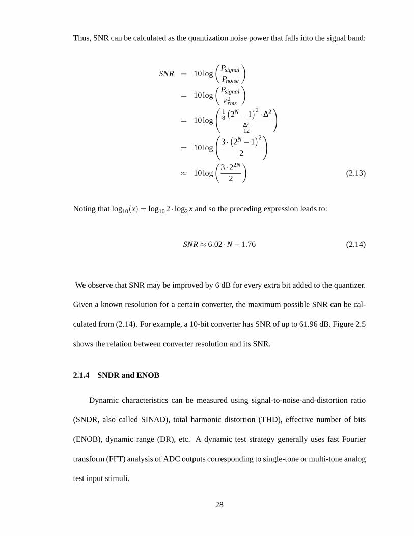
Thus, SNR can be calculated as the quantization noise power that falls into the signal band:
SNR = 10log
(
Psignal
Pnoise
)
= 10log
(
Psignal
e2rms
)
= 10log
(
18
(
2N −1)2 ·∆2
∆2
12
)
= 10log
(
3·(
2N −1)2
2
)
≈ 10log
(
3·22N
2
)
(2.13)
Noting that log10(x) = log102· log2x and so the preceding expression leads to:
SNR≈ 6.02·N+1.76 (2.14)
We observe that SNR may be improved by 6 dB for every extra bit added to the quantizer.
Given a known resolution for a certain converter, the maximum possible SNR can be cal-
culated from (2.14). For example, a 10-bit converter has SNRof up to 61.96 dB. Figure 2.5
shows the relation between converter resolution and its SNR.
2.1.4 SNDR and ENOB
Dynamic characteristics can be measured using signal-to-noise-and-distortion ratio
(SNDR, also called SINAD), total harmonic distortion (THD),effective number of bits
(ENOB), dynamic range (DR), etc. A dynamic test strategy generally uses fast Fourier
transform (FFT) analysis of ADC outputs corresponding to single-tone or multi-tone analog
test input stimuli.
28
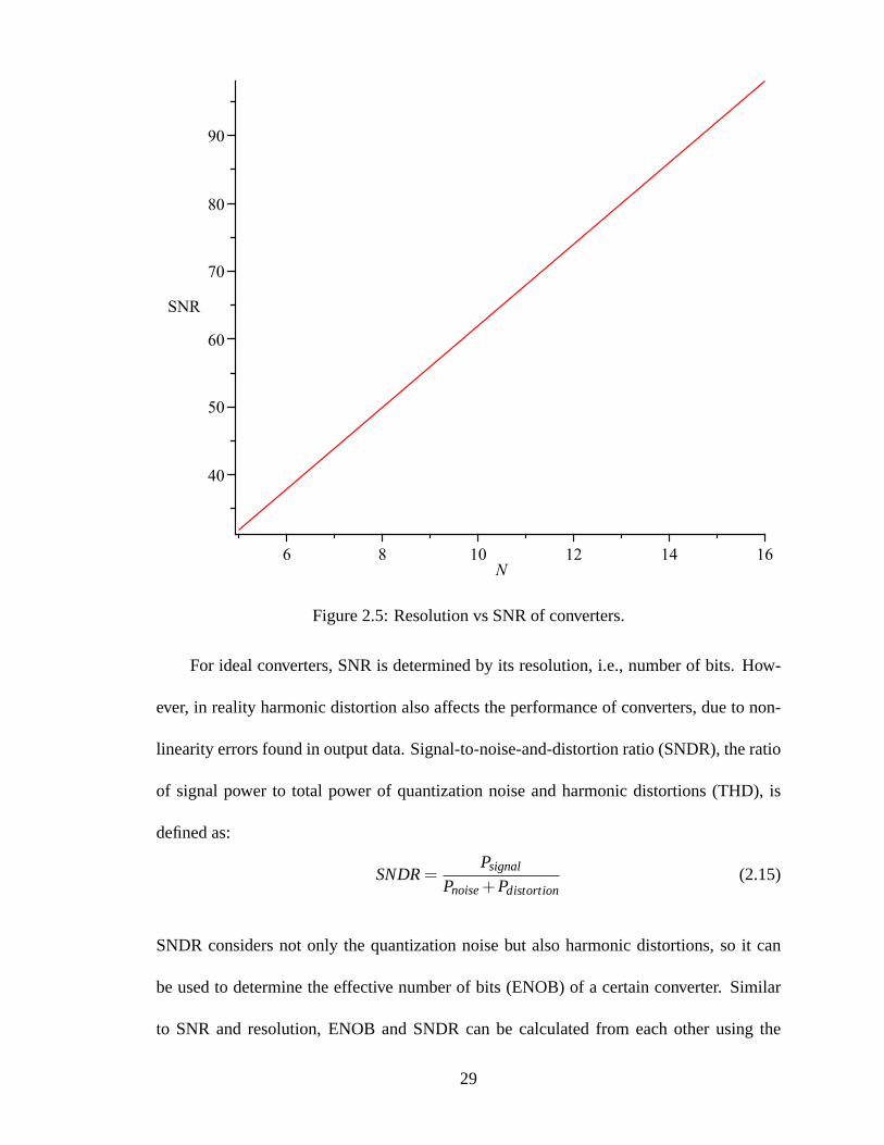
Figure 2.5: Resolution vs SNR of converters.
For ideal converters, SNR is determined by its resolution, i.e., number of bits. How-
ever, in reality harmonic distortion also affects the performance of converters, due to non-
linearity errors found in output data. Signal-to-noise-and-distortion ratio (SNDR), the ratio
of signal power to total power of quantization noise and harmonic distortions (THD), is
defined as:
SNDR=Psignal
Pnoise+Pdistortion(2.15)
SNDR considers not only the quantization noise but also harmonic distortions, so it can
be used to determine the effective number of bits (ENOB) of a certain converter. Similar
to SNR and resolution, ENOB and SNDR can be calculated from each other using the
29

following equation:
SNDR= 6.02·ENOB+1.76 (2.16)
2.2 Summary
In this chapter, some fundamental characteristics that measure the performance of
ADC and DAC are discussed and the background for mixed-signal testing is given. Al-
though mixed-signal IC and SoC usually consist of fewer components as compared to
digital circuits, testing mixed-signal devices is more complex because here one adopts a
specification-oriented approach instead of the defect-oriented approach used by digital test-
ing techniques. Due to their complexity, most of the well-studied digital testing techniques
cannot be directly applied to mixed-signal testing and their relevant characteristics must be
understood to find ways to test the mixed-signal circuitry.
30
Chapter 3
BIST Architecture for Mixed-Signal Devices
In this chapter, a newly proposed fully digital ADC self-test approach is discussed and
compared with the conventional ADC test methods. This complete digital test flow takes
advantage of test signals from a digital signal processor (DSP), which can be programmed
to generate various test patterns, e.g., maximum/minimum,ramp, triangle, single-tone si-
nusoid, or multi-tone sinusoidal codes. Different test patterns can be used for static or
dynamic response analysis to measure the ADC performance.
3.1 Test of Mixed-Signal Devices
3.1.1 ADC/DAC Test Methods
To characterize high-resolution ADC/DAC, accurate stimuli must be generated to
measure both static and dynamic performances. Most conventional test methods for on-
chip ADC in mixed-signal SoC fall into two types. Some production test approaches em-
ploying analog or mixed-signal automatic test equipment (ATE), which generates high-
precision analog test signals externally. While providing good quality test signals, such
external test equipment is expensive, offers only off line application and usually requires a
relatively long test time.
31
TPG
ORA
TEST CO N TRO L
MUX
MUX
DAC
ADC
MIXED SIGNAL
MUX
ANALO G SYSTEM
ANALO G SYSTEM
MUX
BIST Results
Digital System
Input and Output
Analog System
Input and
Output
Analog Loopbacks
DSP
DIGITAL SYSTEM
Dig
ital l
oo
pb
ack
Digital input
Loopback controls
Test pattern control
Response control
Digital outputAnalog signals
An
alo
g lo
op
ba
ck
An
alo
g s
yste
m lo
op
ba
ck
Analog output
Analog input
under−test
under−test
under−test
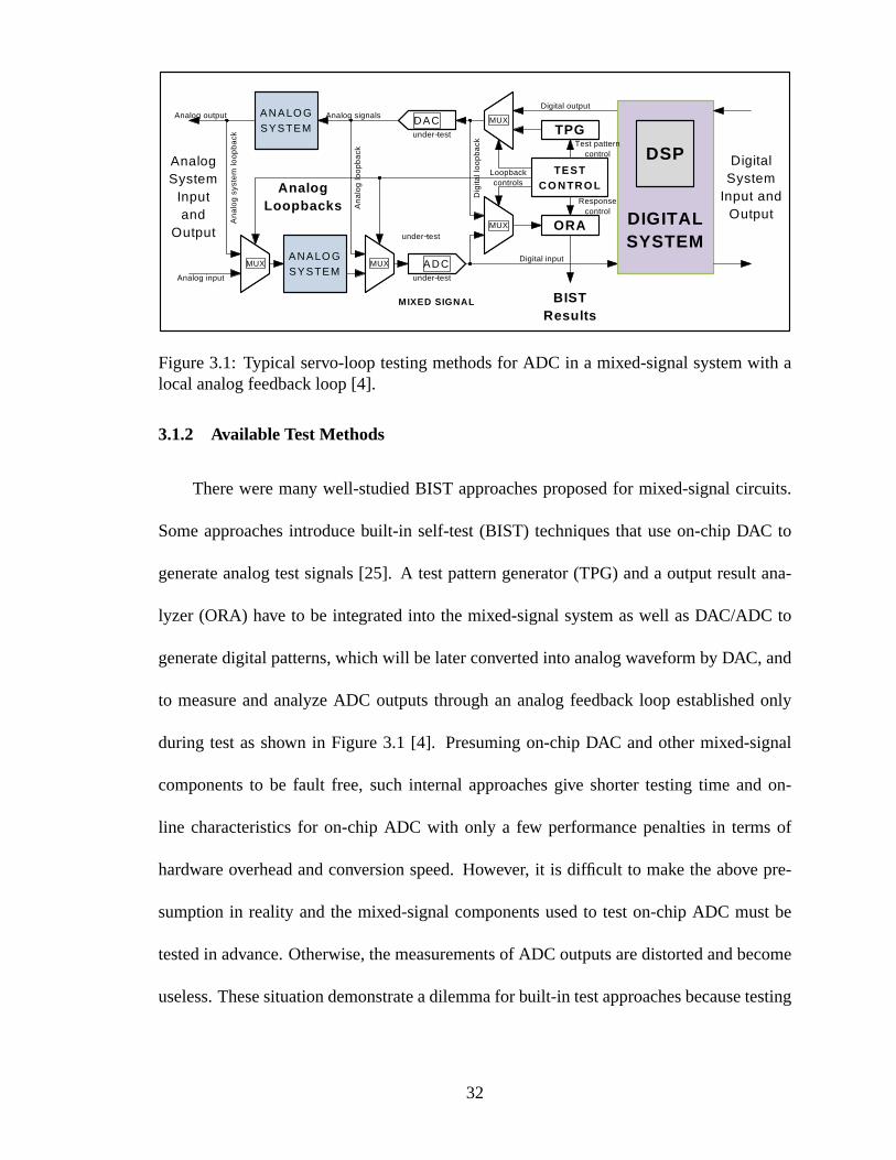
Figure 3.1: Typical servo-loop testing methods for ADC in a mixed-signal system with alocal analog feedback loop [4].
3.1.2 Available Test Methods
There were many well-studied BIST approaches proposed for mixed-signal circuits.
Some approaches introduce built-in self-test (BIST) techniques that use on-chip DAC to
generate analog test signals [25]. A test pattern generator(TPG) and a output result ana-
lyzer (ORA) have to be integrated into the mixed-signal system as well as DAC/ADC to
generate digital patterns, which will be later converted into analog waveform by DAC, and
to measure and analyze ADC outputs through an analog feedback loop established only
during test as shown in Figure 3.1 [4]. Presuming on-chip DACand other mixed-signal
components to be fault free, such internal approaches give shorter testing time and on-
line characteristics for on-chip ADC with only a few performance penalties in terms of
hardware overhead and conversion speed. However, it is difficult to make the above pre-
sumption in reality and the mixed-signal components used totest on-chip ADC must be
tested in advance. Otherwise, the measurements of ADC outputs are distorted and become
useless. These situation demonstrate a dilemma for built-in test approaches because testing
32
of either DAC or ADC requires the other part to be fault free aswell as a working analog
loopback connection [28].
In some situations, this on-chip DAC may need additional high-resolution ADC to
test [29]. A recent paper [26] has proposed a self-calibration approach to make fixes to
ADC and DAC outputs to achieve better linear outputs, requiring both on-chip ADC and
DAC. Additional self-test of measuring ADC must be done priorto test and calibration of
other on-chip components, otherwise the extracted parameters are not precise and compen-
sating signals cannot be correctly generated. If a DAC is notpresent on the target mixed-
signal SoC, noise could be used as test signal for BIST of ADC [30], requiring significant
power consumption by digital circuitry. In another method [31], digital control logic is
used to generate voltage oscillation for full-range ramp test of ADC without DAC. This
method can be used for DNL, INL and gain error testing. However, the measured perfor-
mances heavily rely on the linearity of the current source and capacitance which generate
ramp signals.
3.1.3 Servo-Loop Testing Method
Conventional built-in ADC test approaches, as shown in Figure 3.1, require test cir-
cuitry including test pattern generator (TPG), output results analyzer (ORA), a built in
(presumed fault-free) DAC and a local feedback loop link established between DAC and
ADC during BIST. Such approaches are called servo-loop methods and usually perform
a full-scale histogram test on ADC-under-test to measure linearity responses of the ADC.
To properly test on-chip ADC, the DAC required by conventional ADC test methods must
33
be of same or higher resolution than that of the ADC. TPG can also be used to generate
various forms of test signals for dynamic response tests.
A three-step testing procedure must be performed in order tocomplete servo-loop test
on ADC-under-test.
• Perform BIST on digital circuitry at first
• Establish a digital link between TPG and ORA, and perform a digital test on TPG/ORA
directly
• Establish an analog link between DAC and ADC, and perform an mixed-signal test
on ADC
It is obvious that the servo-loop approach is complex and slow, requires an on-chip
high-resolution DAC, and multiple loopback links have to be established/disconnected dur-
ing different steps of test. The DAC is the most critical partin the approach because low-
resolution DAC cannot satisfy the minimum requirements of ADC. DAC with lower res-
olution is easier to manufacture and control, and generallyhas lower cost, however, such
low-resolution DAC is unable to cover full-scale of ADC-under-test and majority of the
codes cannot be tested. On the other hand, high-resolution DAC may be sufficient to test
ADC but it is more expensive to design and manufacture, and itis more difficult to control
its linearity and noise figure.
The test performance relies on the design of a presumed fault-free DAC; otherwise
it may result in incorrect measurements and wrong characteristics. For static response
test, ideal digital test patterns generated by TPG will no longer be ideal after they are
converted into analog signals by DAC. Any nonlinearity errors in either DAC or ADC will
34
be measured but considered only as nonlinearity errors of ADC. For dynamic response
test, transfer function of DAC will distort ideal test patterns and inject additional noise into
the single-tone or multiple-tone sinusoidal signals. Thus, the usage of a DAC should be
removed from ADC test procedures to avoid such unexpected nonlinearity errors, noise
and distortions caused by the DAC to correctly measure and characterize the ADC-under-
test.
3.1.4 Sigma-Delta Testing Method
A sigma-delta modulation based BIST scheme has been presented for mixed-signal
circuits [32]. Oversampling sigma-delta modulation was employed for both stimulus gen-
eration and response analysis to achieve high-quality stimuli and measurement without
stringent hardware requirement. This approach also requires higher-resolution stimuli gen-
erator and multi-bit digital streams to measure the function (approximately, 6dB per bit).
A software based multi-bit sigma-delta encoder is used to compensate for DAC imperfec-
tions. The approach depends on software to complete the BIST and provide compensation
and its performance is a concern. The existence of multiple sigma-delta modulators in this
approach is another concern, which may increase the design complexity and overhead of
the BIST circuit.
Leeet al.[33] proposed a sigma-delta modulation based BIST scheme to concurrently
generate analog sinusoidal test stimuli and digital sinusoidal reference signals. CUT is sup-
plied the analog stimuli and then four key parameters of ADC, namely,offset error, gain
error, integral nonlinearity erroranddifferential nonlinearity error, are measured against
digital reference based on sinusoidal histogram of ADC output. This approach can provide
35
high accuracy and low chip area overhead for 8-bit ADCs. But fortesting higher-resolution
ADC, it may be difficult to produce analog and digital signals simultaneously and sigma-
delta modulator would require more clock cycles leading to areduce overall performance.
The histogram method used in the scheme also requires much larger overhead for additional
memory space for storing data. Onget al. [34] give a second-order delta-sigma modula-
tor based mixed-signal BIST architecture capable of testing/characterizing itself using all
digital stimulus. Test time of the architecture is shorter than the static linear ramp testing.
However, it heavily depends on DSP processor for generatingdigital stimulus, filtering the
results from delta-sigma modulator, performing fast Fourier transform (FFT) and charac-
terizing the modulator.
There are other similar solutions using Sigma-Delta techniques [35, 36, 37, 38, 39, 40,
41, 42, 43, 44, 45, 46, 47, 48].
3.1.5 Histogram Testing Method
Histogram methods are often used in BIST schemes for DAC/ADC. Wang et al. [49]
present a low-cost BIST based on linear histogram for testingon-chip ADC with paral-
lel time decomposition technique to minimize area overheadand test time. Several au-
thors [29, 50] use dithering techniques to obtain precise analog signals for high quality
stimuli generation. However, it is difficult to apply the histogram testing method to high-
resolution ADC because of the large amount of samples to be collected and the long test
time that leads to. The method also needs a very slow-slope ramp signal or low-frequency
sinusoidal test signals. In BIST, these requirements eitherare impractical to design or cause
high overhead.
36
Histogram testing method is widely used for determination of nonlinearity errors of
ADC as an alternative of servo-loop method. The excitation signals for ADC under test can
be either a low-slope ramp signal or a low-frequency sinusoidal wave, but usually a ramp
signal is used because histogram test with ramp signals (or equivalent triangular signals) is
significantly faster than that with sinusoidal signals. Whennoise figure is comparable to
ADC measurement accuracy and all conversion codes need to betested, ramp histogram
testing method is faster than servo-loop testing method andalso has lower overhead and
testing costs.
The histogram testing method requires an accurate and highly linear ramp signal to
correctly test ADC under test. Any non-ideal factors in ramptesting signals, e.g., quanti-
zation errors, device parameter variances, or unbalanced elements, will influence the mea-
sured ADC output codes and therefore have an impact on the transfer function of ADC. For
example, to test a 16-bit ADC to 1/8LSB accuracy requires a ramp with 19 bits of resolu-
tion and overall linearity error of better than 2 ppm. A histogram ramp testing of ADC has
been proposed [51] for imperfect ramp signals by measuring more samples per code. In a
typical case, 14 samples are needed for each code and 10,000 codes in total would then be
about 140,000 samples, which require about 140ms to performthe full range testing of an
ADC with conversion speed of 1µs.
However, the histogram ramp testing method of this type cannot be easily applied
to high-resolution ADCs because of the large amount of possible measured code by such
ADCs. Considering in the same typical case, 14 samples are needed for an ADC with 16-bit
resolution which has 65,536 possible codes in total and thenrequired testing time is close
37
to 1s. Furthermore, generally a high-resolution ADC is significantly slower than a lower-
resolution ADC and thus the required testing time would be much longer if conventional
histogram ramp testing method is used.
Assuming anN-bit ADC with converting speed ofSsamples per second and average
K samples per code for a reduced error margin, the total testing time for such an ADC using
the histogram method is:
T =K2N
S(3.1)
Very low-slope ramp testing signals are also required to measure each possible code by
ADC under test. Ramp signal generator typically consists of acurrent source(I) and a
capacitance(C), and the open loop output voltage isV = I · t/C. Further, assuming that the
ADC measuring range isV volts, the ramp slope and current are:
∆V =VT
=VSK2N
I =CVT
=VSCK2N (3.2)
Suppose,V = 3.3V andC = 47pF for a typical design with reasonable testing hardware
overhead, the calculated current source is only about 0.15nA from (3.2), which is compa-
rable to the background noise and hence impractical for realdesigns. Thus, both situations
are unacceptable in most applications.
The errors introduced during a histogram test method are classified into two cate-
gories: deterministic errors for inaccuracy and random errors for uncertainty of measured
results. The ADC output is a combination of these two kinds oferrors. In characterizing
38
DSP
ADC
under-test
DAC
under-test
m-ADC
Signal
Generator
Analog
System
d-DACPolynomial
evaluation
N
N
NDiagnosis
TPG
TPG
Figure 3.2: The proposed mixed-signal BIST architecture fortesting both ADC and DAC.
ADC by measured results, the deterministic errors can be obtained by calculated coeffi-
cients because random errors will be greatly reduced by accumulation of measurements.
Therefore, a minimal number of measurements must be determined.
3.2 Proposed Approaches
There are several papers that discuss mixed-signal testingtechniques for ADC and
DAC [16, 52]. In this dissertation, a post-fabrication mixed-signal BIST architecture is
proposed for testing ADC/DAC and analog circuitry. Before themixed-signal BIST starts,
the proposed method requires that digital circuitry, including DSP and other peripheral dig-
ital logic, must have passed digital BIST and therefore we canassume that digital circuitry
is fault-free and able to generate desired digital signals without any error.
After digital circuitry is tested and verified to be fault free by digital BIST architecture,
for example, logic BIST, memory BIST, scan chains, etc., the mixed-signal BIST will start
for testing of DAC/ADC and then for testing of analog circuitry. The proposed mixed-
signal BIST architecture, as shown in Figure 3.2, includes three additional major parts for
39
testing ADC and DAC. These parts include an analog signal generator, a high-resolution
measuring ADC and a low-resolution dithering DAC.
3.3 Testing Steps of BIST Architecture
The proposed mixed-signal BIST architecture includes four major steps to complete
full-range self-test and calibration for on-chip ADC and DAC. Prior to the mixed-signal
BIST, all digital circuitry must have passed digital test procedures, which has been already
well studied and beyond the discussion topic in this thesis.The most widely employed
digital test techniques that can be used for digital part of the mixed-signal system include
logic BIST, scan chain, and cell/chip-level boundary scan. After digital circuitry passes
its own digital testing procedure, it can be considered fault-free so that it will generate
desired and correct digital data which in turn will be used for following mixed-signal testing
procedures proposed in this thesis.
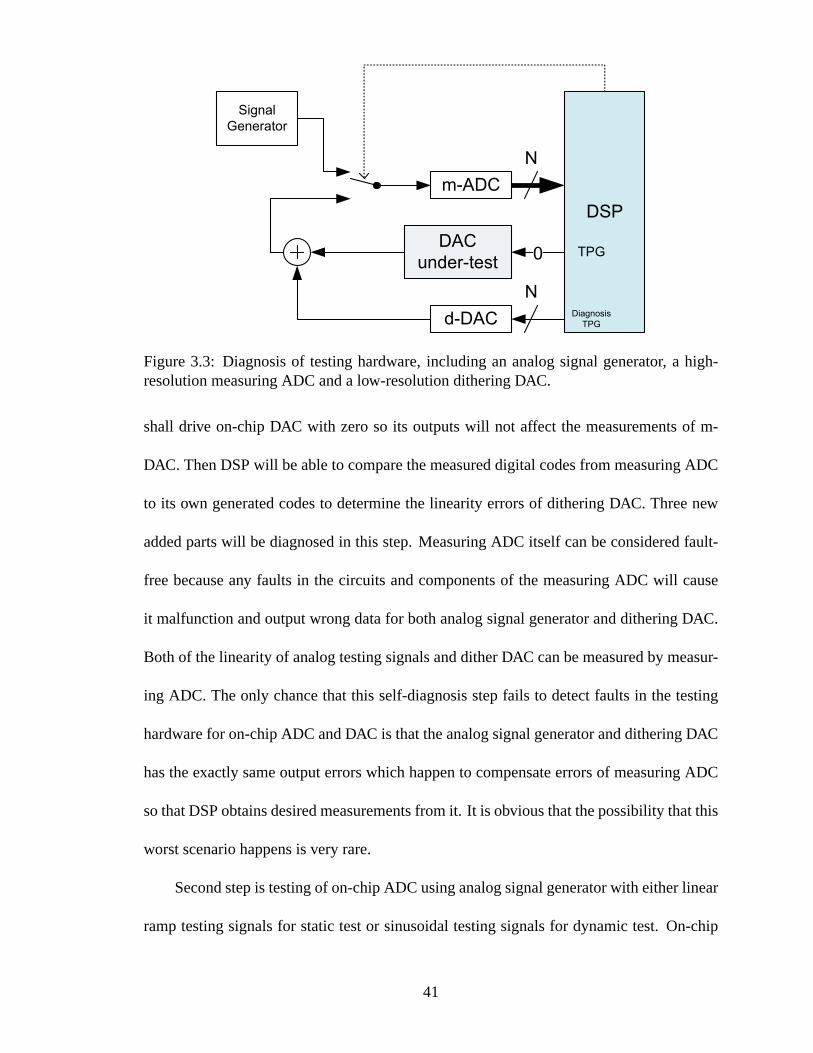
First step of the proposed BIST architecture is diagnosis of newly added testing hard-
ware for on-chip ADC and DAC, as shown in Figure 3.3. A loopbackconnection may be
established between analog signal generator and measuringADC so that DSP can measure
analog testing signals by measuring ADC. The results that DSPgets from measuring ADC
shall be a rising consecutive codes and a simple histogram may be constructed to evaluate
linearity of analog signal generator. A second loopback connection then can be established
between dithering DAC and measuring ADC to measure dither DAC outputs. DSP will
generate rising consecutive codes, which is converted intoanalog ramp signals by dither-
ing DAC and then back into digital codes in turn by measuring ADC. During this test, DSP
40
DSP
DAC
under-test
m-ADC
Signal
Generator
d-DAC
0
N
NDiagnosis
TPG
TPG
Figure 3.3: Diagnosis of testing hardware, including an analog signal generator, a high-resolution measuring ADC and a low-resolution dithering DAC.
shall drive on-chip DAC with zero so its outputs will not affect the measurements of m-
DAC. Then DSP will be able to compare the measured digital codes from measuring ADC
to its own generated codes to determine the linearity errorsof dithering DAC. Three new
added parts will be diagnosed in this step. Measuring ADC itself can be considered fault-
free because any faults in the circuits and components of themeasuring ADC will cause
it malfunction and output wrong data for both analog signal generator and dithering DAC.
Both of the linearity of analog testing signals and dither DACcan be measured by measur-
ing ADC. The only chance that this self-diagnosis step fails to detect faults in the testing
hardware for on-chip ADC and DAC is that the analog signal generator and dithering DAC
has the exactly same output errors which happen to compensate errors of measuring ADC
so that DSP obtains desired measurements from it. It is obvious that the possibility that this
worst scenario happens is very rare.
Second step is testing of on-chip ADC using analog signal generator with either linear
ramp testing signals for static test or sinusoidal testing signals for dynamic test. On-chip
41
ADC will measure generated analog signals and DSP will analyze the measurement for
characterizing the ADC-under-test. It shall be noted that the analog signal generator must
have been reset to zero before performing this step to make sure the results is not affected
by its current status due to the previous step. DSP is occupied during the test and cannot
run other tasks.
Third step is testing of on-chip DAC using DSP as both test pattern generator and
output data analyzer which takes the output data from measuring ADC and characterizes
the DAC-under-test. Digital test patterns generated by DSP can be of any form, however,
in most cases ramp signal and sinusoidal signal are used for static and dynamic tests re-
spectively. Multiple-tone sinusoidal signals can also be used to measure the third-order
intermodulation (IM3), and linearity measured using third-order intercept point (IP3) [53].
DSP is occupied during the step too because it generate test patterns and analyze results.
The last step is calibration of on-chip DAC using dithering DAC that will generate
negative compensating analog signals for every analog outputs of DAC-under-test so that
the nonlinearity errors can be reduced, if not removed completely, from the final output of
on-chip DAC. The compensation signals are calculated from characteristics of the DAC-
under-test measured by measuring ADC. Dithering DAC can be driven with compensating
values from either DSP directly or a hardware implementation which takes digital output
codes.
In summary, testing steps for the proposed mixed-signal BISTarchitecture are:
1. Diagnosis of newly added testing hardware;
2. Testing of on-chip ADC using analog testing signals;
3. Testing of on-chip DAC using embedded DSP and measuring ADC;
42
4. Calibration of on-chip DAC using dithering DAC.
5. Validation of calibrated DAC using on-chip ADC
3.4 Components of BIST Architecture
3.4.1 Analog Signal Generator
An analog signal generator, usually linear ramp signal generator with very low gain to
cover the full-scale of ADC input range, is used to generate analog testing signals for on-
chip ADC. A sinusoidal signal generator can also be used in theplace to generate very low
frequency sine waves for testing on-chip ADC. ADC-under-testwill measure the testing
signals from the signal generator and samples will be pickedup by DSP for analysis and
characterization of the ADC.
If linear ramp testing signals are used, DSP will perform a static testing procedure,
which is useful to obtain characteristics of ADC like nonlinearity errors, gain, offset and
other harmonic distortions. If sine wave testing signals are used instead, DSP will perform a
dynamic testing procedure to analyze the frequency response of the ADC, dynamic range,
and other distortions. One of these two analog signal generator have to be chosen for a
certain chip based on its application and working environment.
A linear ramp signal generator is easy to design and generates small footprint in die
so the hardware overhead is lower. A sinusoidal signal generator is complex comparing
to ramp generator, but it is capable of performing much more testing and measurements
for different frequency. Single-tone sine wave signal can be used for analysis of frequency
responses of a wide range so that more accurate characteristics, such as gain, offset and
harmonic distortions can be acquired. Multiple-tone sine wave can also be used for analysis
43
of intermodulation distortions between two frequencies toobtain nonlinear characteristics,
usually third-order intermodulation of two frequencies.
Here we will discuss the design of a linear ramp signal generator which is implemented
for my thesis research.
Usually a ramp signal generator is designed using a cascadedcurrent mirror so that
the output ramp signals are linear and stable. W/L ratio of each transistor has to be care-
fully calculated to get desired scaling-down factor to achieve low-slope gain. Some special
considerations must be taken because the load transistor inthe output branch of current
mirror may have a voltage drop so that the output voltage range may not cover full-scale of
operational range of ADC-under-test.
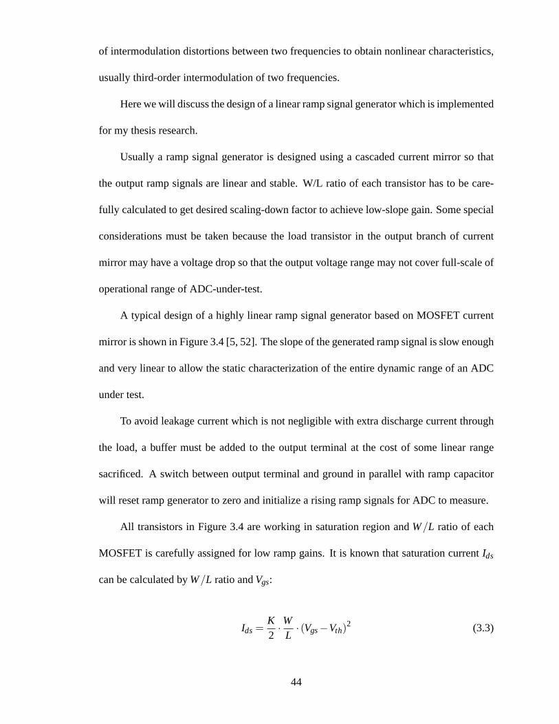
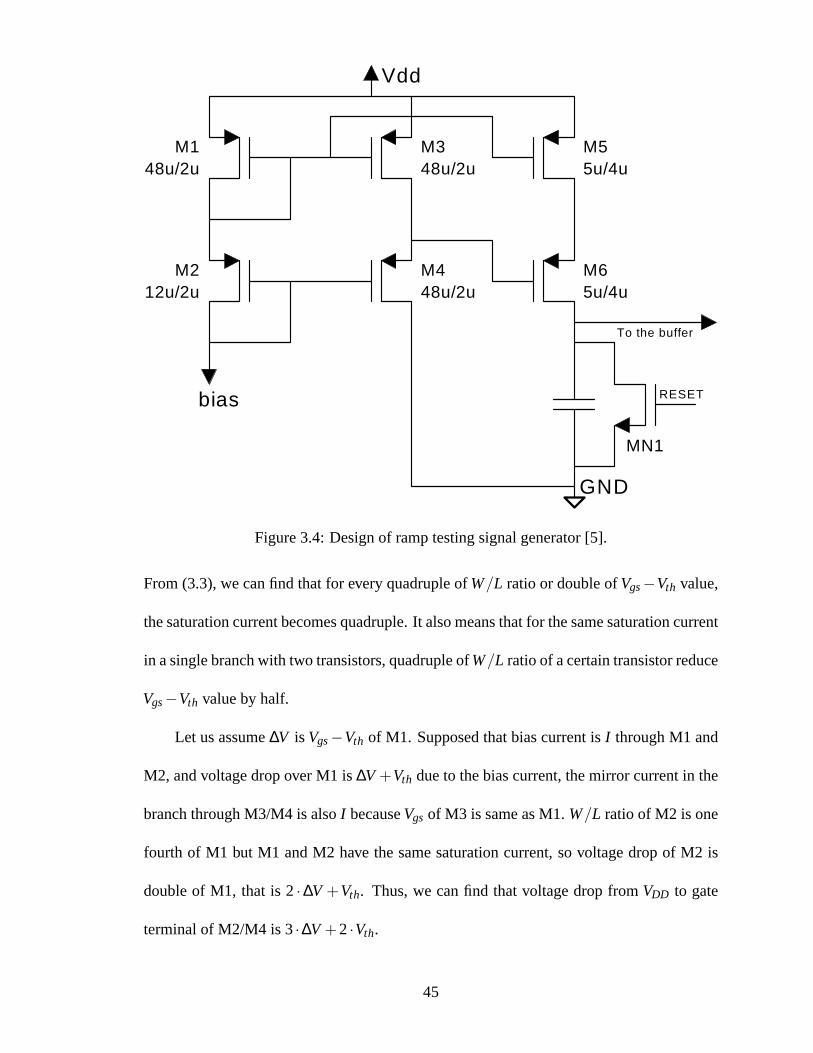
A typical design of a highly linear ramp signal generator based on MOSFET current
mirror is shown in Figure 3.4 [5, 52]. The slope of the generated ramp signal is slow enough
and very linear to allow the static characterization of the entire dynamic range of an ADC
under test.
To avoid leakage current which is not negligible with extra discharge current through
the load, a buffer must be added to the output terminal at the cost of some linear range
sacrificed. A switch between output terminal and ground in parallel with ramp capacitor
will reset ramp generator to zero and initialize a rising ramp signals for ADC to measure.
All transistors in Figure 3.4 are working in saturation region andW/L ratio of each
MOSFET is carefully assigned for low ramp gains. It is known that saturation currentIds
can be calculated byW/L ratio andVgs:
Ids=K2·W
L· (Vgs−Vth)
2 (3.3)
44
bias
Vdd
GND
M148u/2u
M212u/2u
M348u/2u
M55u/4u
M448u/2u
M65u/4u
To the buffer
MN1
RESET
Figure 3.4: Design of ramp testing signal generator [5].
From (3.3), we can find that for every quadruple ofW/L ratio or double ofVgs−Vth value,
the saturation current becomes quadruple. It also means that for the same saturation current
in a single branch with two transistors, quadruple ofW/L ratio of a certain transistor reduce
Vgs−Vth value by half.
Let us assume∆V is Vgs−Vth of M1. Supposed that bias current isI through M1 and
M2, and voltage drop over M1 is∆V +Vth due to the bias current, the mirror current in the
branch through M3/M4 is alsoI becauseVgs of M3 is same as M1.W/L ratio of M2 is one
fourth of M1 but M1 and M2 have the same saturation current, sovoltage drop of M2 is
double of M1, that is 2·∆V +Vth. Thus, we can find that voltage drop fromVDD to gate
terminal of M2/M4 is 3·∆V +2·Vth.
45
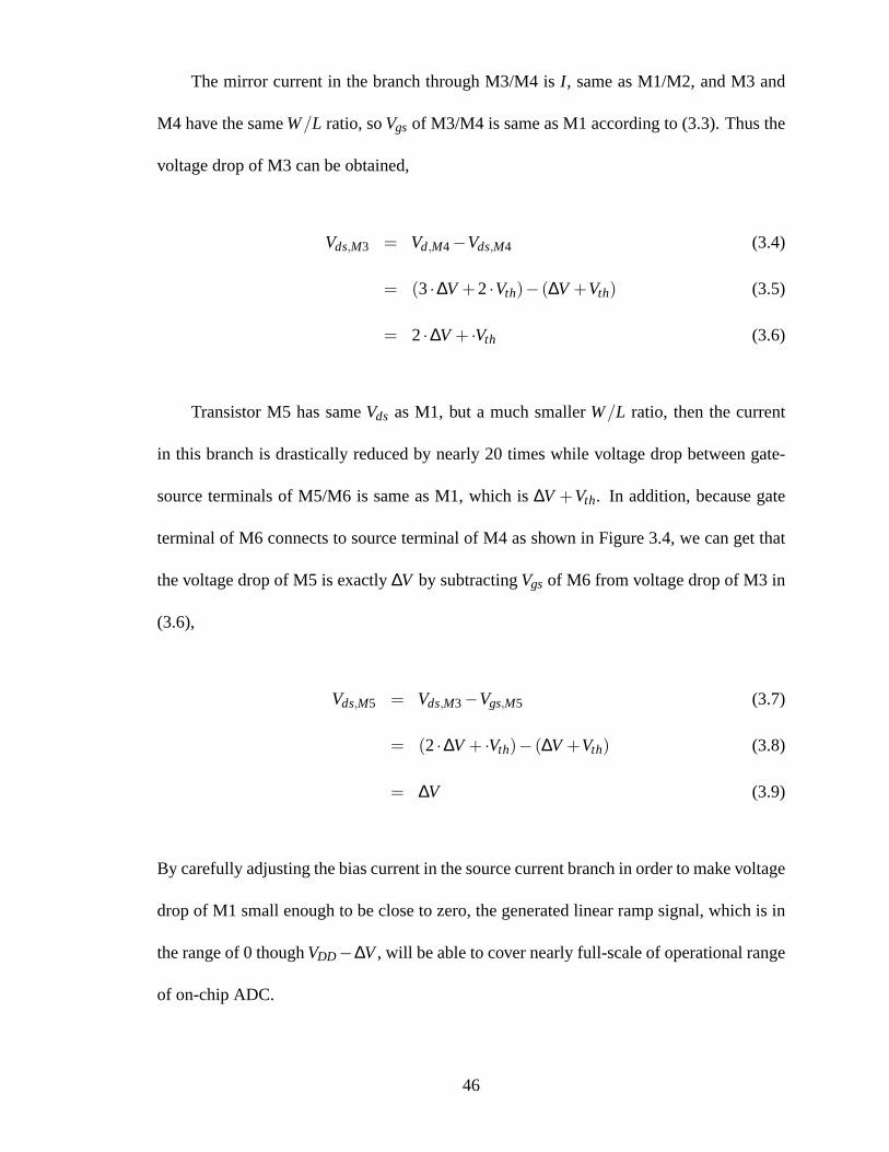
The mirror current in the branch through M3/M4 isI , same as M1/M2, and M3 and
M4 have the sameW/L ratio, soVgs of M3/M4 is same as M1 according to (3.3). Thus the
voltage drop of M3 can be obtained,
Vds,M3 = Vd,M4−Vds,M4 (3.4)
= (3·∆V +2·Vth)− (∆V +Vth) (3.5)
= 2·∆V + ·Vth (3.6)
Transistor M5 has sameVds as M1, but a much smallerW/L ratio, then the current
in this branch is drastically reduced by nearly 20 times while voltage drop between gate-
source terminals of M5/M6 is same as M1, which is∆V +Vth. In addition, because gate
terminal of M6 connects to source terminal of M4 as shown in Figure 3.4, we can get that
the voltage drop of M5 is exactly∆V by subtractingVgs of M6 from voltage drop of M3 in
(3.6),
Vds,M5 = Vds,M3−Vgs,M5 (3.7)
= (2·∆V + ·Vth)− (∆V +Vth) (3.8)
= ∆V (3.9)
By carefully adjusting the bias current in the source currentbranch in order to make voltage
drop of M1 small enough to be close to zero, the generated linear ramp signal, which is in
the range of 0 thoughVDD−∆V, will be able to cover nearly full-scale of operational range
of on-chip ADC.
46
3.4.2 Measuring-ADC
A high-resolution measuring ADC is used for testing on-chipDAC by measuring DAC
outputs and converting analog voltage levels from DAC output to digital codes. DSP then
will compare measured digital results from this high-resolution ADC to generated test pat-
terns for any possible difference.
In order to undergo fine analysis and to obtain results with more accuracy, effective
resolution of the measuring ADC must be higher than that of DAC-under-test. If the mea-
suring ADC cannot meet such resolution requirements, the values of its digital output codes
are not sufficient to determine the errors existing in the DAC-under-test.
Since usually on-chip DAC get digital input codes directly from DSP, the DSP can
act like a test patter generator for the DAC-under-test for both static and dynamic tests.
If DSP generate ramp codes for on-chip DAC, a static test can beperformed to obtain
characteristics of ADC like nonlinearity errors, gain, offset and other harmonic distortions.
In the other hand, if DSP generate approximate sinusoidal codes in sine/cosine wave forms,
then a dynamic test can be done using measured results from measuring ADC to analyze
its frequency response, dynamic range, and other distortions.
Conversion speed, which is a important characteristics for converters in general, is not
a critical issue here for measuring ADC at all. Since such measurements of analog output
signals from on-chip DAC by measuring ADC only be sampled during mixed-signal testing
period, the performance of normal DAC operations after mixed-signal BIST is not affected
by the conversion time of the measuring ADC. Therefore, in order to get more precise
analysis characteristics of DAC-under-test, we can choose as high resolution ADC design
and implementation for the measuring ADC as possible. The only requirement for the
47
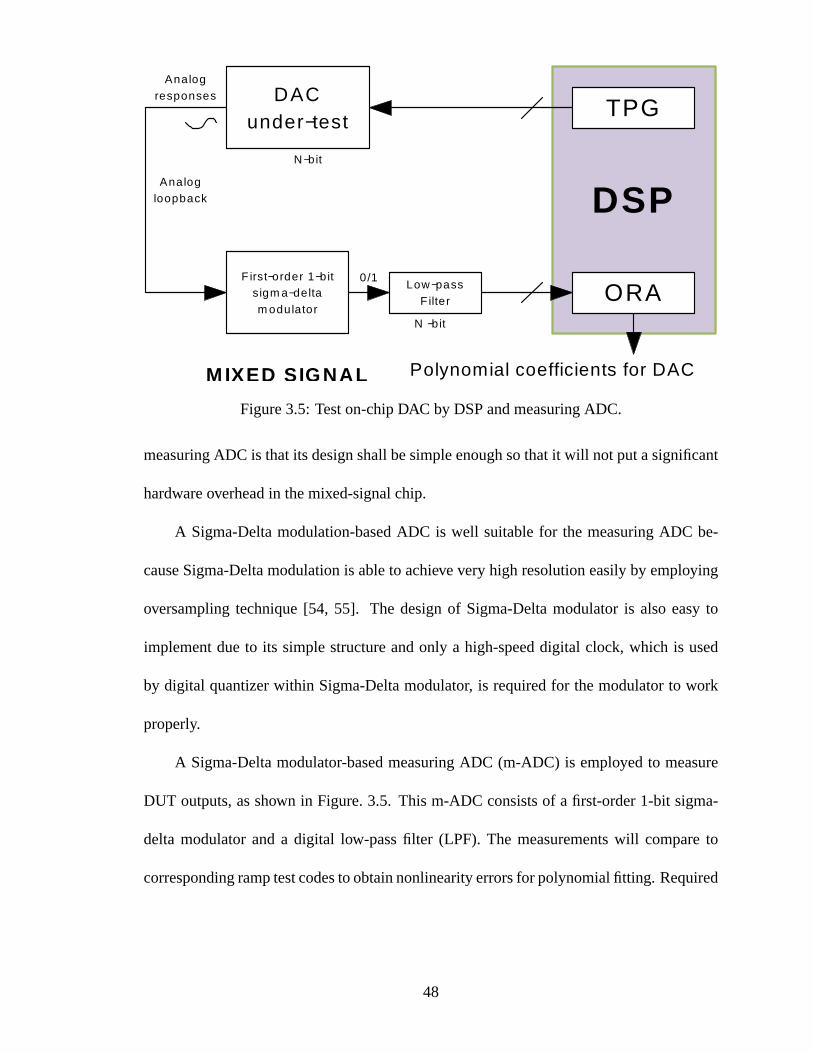
DSP
TPG
ORA
M IXED SIGNAL Polynomial coefficients for DAC
0/1
Analog
responses
Analog loopback
N−bit
N −bit
DACunder−test
Low−pass F ilter
F irst−order 1−bit sigm a−delta
m odulator
Figure 3.5: Test on-chip DAC by DSP and measuring ADC.
measuring ADC is that its design shall be simple enough so that it will not put a significant
hardware overhead in the mixed-signal chip.
A Sigma-Delta modulation-based ADC is well suitable for themeasuring ADC be-
cause Sigma-Delta modulation is able to achieve very high resolution easily by employing
oversampling technique [54, 55]. The design of Sigma-Deltamodulator is also easy to
implement due to its simple structure and only a high-speed digital clock, which is used
by digital quantizer within Sigma-Delta modulator, is required for the modulator to work
properly.
A Sigma-Delta modulator-based measuring ADC (m-ADC) is employed to measure
DUT outputs, as shown in Figure. 3.5. This m-ADC consists of afirst-order 1-bit sigma-
delta modulator and a digital low-pass filter (LPF). The measurements will compare to
corresponding ramp test codes to obtain nonlinearity errors for polynomial fitting. Required
48
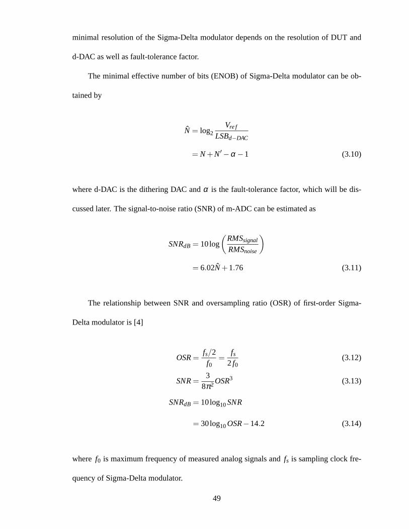
minimal resolution of the Sigma-Delta modulator depends onthe resolution of DUT and
d-DAC as well as fault-tolerance factor.
The minimal effective number of bits (ENOB) of Sigma-Delta modulator can be ob-
tained by
N = log2Vre f
LSBd−DAC
= N+N′−α −1 (3.10)
where d-DAC is the dithering DAC andα is the fault-tolerance factor, which will be dis-
cussed later. The signal-to-noise ratio (SNR) of m-ADC can beestimated as
SNRdB = 10log
(
RMSsignal
RMSnoise
)
= 6.02N+1.76 (3.11)
The relationship between SNR and oversampling ratio (OSR) offirst-order Sigma-
Delta modulator is [4]
OSR=fs/2f0
=fs
2 f0(3.12)
SNR=3
8π2OSR3 (3.13)
SNRdB = 10log10SNR
= 30log10OSR−14.2 (3.14)
where f0 is maximum frequency of measured analog signals andfs is sampling clock fre-
quency of Sigma-Delta modulator.
49
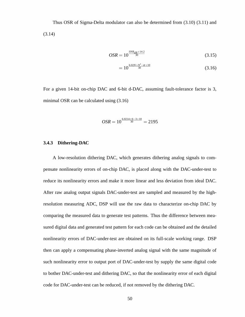
Thus OSR of Sigma-Delta modulator can also be determined from (3.10) (3.11) and
(3.14)
OSR= 10SNRdB+14.2
30 (3.15)
= 106.02N+N′−α+10
30 (3.16)
For a given 14-bit on-chip DAC and 6-bit d-DAC, assuming fault-tolerance factor is 3,
minimal OSR can be calculated using (3.16)
OSR= 106.0214+6−3+10
30 = 2195
3.4.3 Dithering-DAC
A low-resolution dithering DAC, which generates dithering analog signals to com-
pensate nonlinearity errors of on-chip DAC, is placed along with the DAC-under-test to
reduce its nonlinearity errors and make it more linear and less deviation from ideal DAC.
After raw analog output signals DAC-under-test are sampled and measured by the high-
resolution measuring ADC, DSP will use the raw data to characterize on-chip DAC by
comparing the measured data to generate test patterns. Thusthe difference between mea-
sured digital data and generated test pattern for each code can be obtained and the detailed
nonlinearity errors of DAC-under-test are obtained on its full-scale working range. DSP
then can apply a compensating phase-inverted analog signalwith the same magnitude of
such nonlinearity error to output port of DAC-under-test by supply the same digital code
to bother DAC-under-test and dithering DAC, so that the nonlinearity error of each digital
code for DAC-under-test can be reduced, if not removed by the dithering DAC.
50
Since what dithering DAC is designed to remove are nonlinearity errors of on-chip
DAC, which is much smaller analog value than DAC output valuesthemselves, the dither-
ing DAC is not necessary to be a high resolution one. Output analog values from dithering
DAC must be scaled down to the magnitude of LSB of on-chip DAC, in order to compen-
sate such nonlinearities of DAC-under-test. The exact required resolution of this dithering
DAC depends on testing accuracy and tolerance of nonlinearity errors specified by on-chip
DAC.
Usually dithering DAC with higher resolution is useful to gives better compensating
results and larger range of nonlinearity tolerance so that both output signals quality and
fixable errors are improved in theory. However, higher resolution design of DAC also
means the complexity of dithering DAC increases dramatically and dithering DAC itself
may be found more nonlinearity errors which would affect thefinal output signal quality of
on-chip DAC in practice. Given a mixed-signal BIST application with certain on-chip DAC
and measuring ADC, we have to make trade-off between testing accuracy and tolerance of
nonlinearity errors by choosing proper resolution of dithering DAC and scaling-down factor
of compensating signals for its outputs signals.
After the order and polynomials of best matching fitting polynomial are determined,
they will be compared to pre-defined values. INL errors of DUTare correctable only if the
polynomial coefficients are within the specified range; otherwise DUT will be marked as
faulty by DSP. For correctable DUT, the fitting polynomial and its coefficients will be saved
into memory cells and retrieved by polynomial evaluation circuit to generate correcting
codes.
51
DSP
MIXED SIGNALPolynom ial
coefficients for DAC
x
y
A na log
co rrec tion s igna l
D ig ita l ou tpu tC orrec te d
ana lo g
ou tpu t
DACunder−test
d−DACBest matching
poly eval
Figure 3.6: DUT calibration by dithering DAC (d-DAC) and bestmatching polynomial.
A low-resolution low-cost dithering DAC (d-DAC) will convert such correcting codes
into correcting analog signals to remove nonlinearity errors from DUT output, as shown in
Figure 3.6. Low-resolution d-DAC is simple to design and manufacture cost if low while
converting speed is high. Higher-resolution d-DAC may generate more accurate correcting
signals if total delay of polynomial evaluation circuit andd-DAC is less than converting
time of DUT and such hardware overhead is acceptable. The reference voltage of d-DAC
is defined by the resolution of DUT and fault-tolerance factor.
Vre f,d−DAC =±2α
2·LSB
=±2α
2· 2Vre f
2N =±2α−N ·Vre f (3.17)
LSBd−DAC =2Vre f,d−DAC
2N′
= 21+α−N−N′ ·Vre f (3.18)
for N-bit DAC-under-test with reference voltageVre f ,N′-bit d-DAC, and fault-tolerance
factorα.
In most case, it is sufficient to chooseα equal to 3 and to use 6-bit d-DAC for DUT
correction. Thus for given 14-bit DAC-under-test, the reference voltage and LSB of d-DAC
52
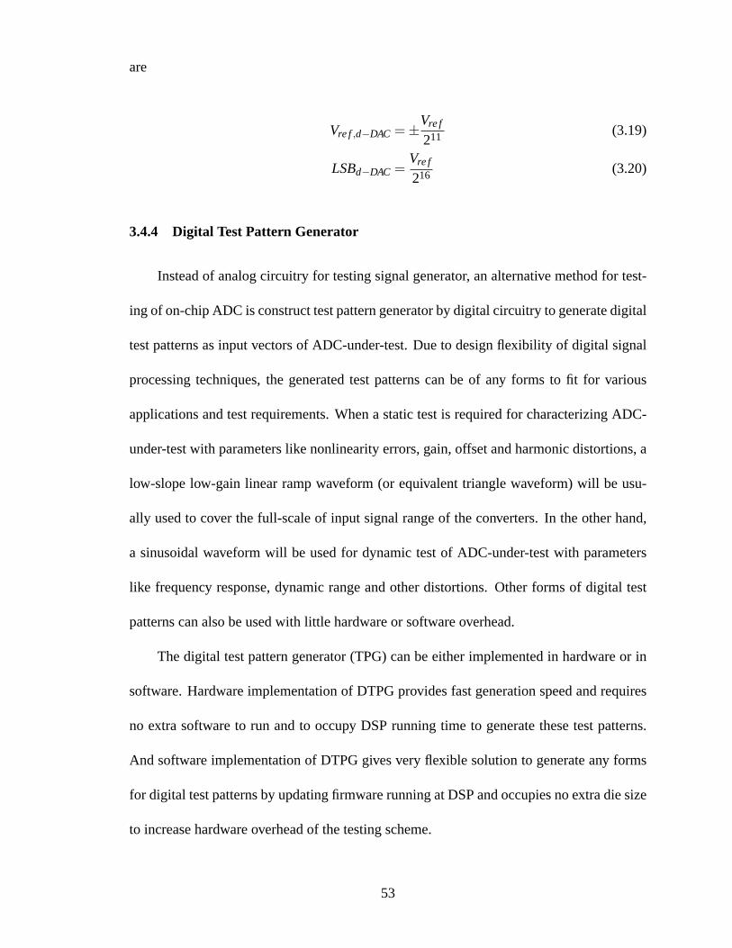
are
Vre f,d−DAC =±Vre f
211 (3.19)
LSBd−DAC =Vre f
216 (3.20)
3.4.4 Digital Test Pattern Generator
Instead of analog circuitry for testing signal generator, an alternative method for test-
ing of on-chip ADC is construct test pattern generator by digital circuitry to generate digital
test patterns as input vectors of ADC-under-test. Due to design flexibility of digital signal
processing techniques, the generated test patterns can be of any forms to fit for various
applications and test requirements. When a static test is required for characterizing ADC-
under-test with parameters like nonlinearity errors, gain, offset and harmonic distortions, a
low-slope low-gain linear ramp waveform (or equivalent triangle waveform) will be usu-
ally used to cover the full-scale of input signal range of theconverters. In the other hand,
a sinusoidal waveform will be used for dynamic test of ADC-under-test with parameters
like frequency response, dynamic range and other distortions. Other forms of digital test
patterns can also be used with little hardware or software overhead.
The digital test pattern generator (TPG) can be either implemented in hardware or in
software. Hardware implementation of DTPG provides fast generation speed and requires
no extra software to run and to occupy DSP running time to generate these test patterns.
And software implementation of DTPG gives very flexible solution to generate any forms
for digital test patterns by updating firmware running at DSPand occupies no extra die size
to increase hardware overhead of the testing scheme.
53
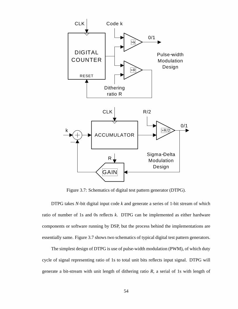
DIGITAL COUNTER
Pulse−width Modulation
Design>R
>k
Code k
Dithering ratio R
RESET
0/1
ACCUMULATOR
CLK
CLK
>R/2
R/2
0/1
GAIN
R
k
Sigma−Delta Modulation
Design
Figure 3.7: Schematics of digital test pattern generator (DTPG).
DTPG takesN-bit digital input codek and generate a series of 1-bit stream of which
ratio of number of 1s and 0s reflectsk. DTPG can be implemented as either hardware
components or software running by DSP, but the process behind the implementations are
essentially same. Figure 3.7 shows two schematics of typical digital test pattern generators.
The simplest design of DTPG is use of pulse-width modulation(PWM), of which duty
cycle of signal representing ratio of 1s to total unit bits reflects input signal. DTPG will
generate a bit-stream with unit length of dithering ratioR, a serial of 1s with length of
54
n1 is output at first, then a serial of 0s with length ofn0. It is obvious thatR= n1+ n0
and duty cycle isn1/R. PWM is easy to implement but suffers serious drawback due to
the imbalance of 1s and 0s in its waveform. So the dithering noise of PWM is widely
distributed and difficult to completely remove because someof the noise is very close to
lower signal band. To separate in-band signals from dithering noise, test pattern frequency
cannot be very high to avoid be interfered by noise. Therefore PWM design of DTPG is
only suitable for applications with low conversion rate ADC.
The other design of DTPG is similar to Sigma-Delta modulation. An accumulator (as
Sigma component in Sigma-Delta modulation) and a comparator (shown as a triangular
component) is used to process input codek. The feedback loop consists of a differential
component and a multiplying factorF (equal to 2N or 0). F depends on the DTPG output,
2N if output is 1, 0 otherwise.k−F is added into the accumulator. DTPG outputs 1 if
accumulator is larger than 2N−1, 0 otherwise. With this design, 1s and 0s of bit-stream
from DTPG output is more likely distributed. Ifk is minimum value 0, DTPG outputs bit-
stream of 0s; ifk is maximum value 2N −1, DTPG outputs bit-stream of 1s. Ifk is other
intermediate value, DTPG will output appropriate number of1s and 0s so that the ratio of
number of 1s toR is equal tok/2N. For examplek = 2N−1, DTPG will output bit-stream
like 010101010101· · · .
Figure 3.8 demonstrate a typical 4-bit ramp pattern and bit-stream for the ramp, of
which digital codek goes from 0 to 24 =16. For N-bit ADC, a total number of 2N ramp
patterns are required for full range static response test sothat every code that ADC can
measure is generated. We may observe that quantization noise is distributed in signal band
and after dithering digital ramp patterns into bit-stream,a high-frequency dithering noise
55
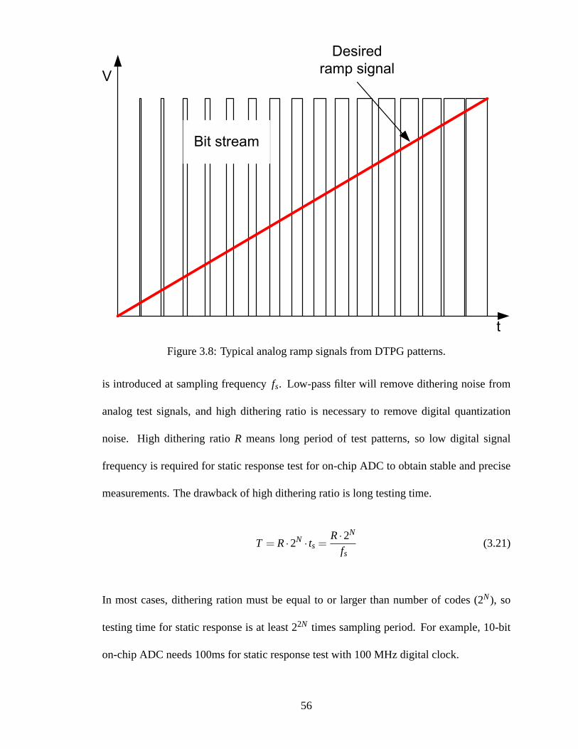
t
V
Bit stream
Desired
ramp signal
Figure 3.8: Typical analog ramp signals from DTPG patterns.
is introduced at sampling frequencyfs. Low-pass filter will remove dithering noise from
analog test signals, and high dithering ratio is necessary to remove digital quantization
noise. High dithering ratioR means long period of test patterns, so low digital signal
frequency is required for static response test for on-chip ADC to obtain stable and precise
measurements. The drawback of high dithering ratio is long testing time.
T = R·2N · ts =R·2N
fs(3.21)
In most cases, dithering ration must be equal to or larger than number of codes (2N), so
testing time for static response is at least 22N times sampling period. For example, 10-bit
on-chip ADC needs 100ms for static response test with 100 MHzdigital clock.
56
A typical single-tone sinusoidal full-range pattern for 10-bit ADC and its dithering
bit-stream can be used for dynamic test. The full-range pattern is generated by DSP and
can be used for dynamic response test at specific digital signal frequency. In fact DSP may
generate arbitrary form of test patterns for various applications. Beside single-tone test
pattern, multiple-tone test patterns can also be used to measure inter-modulation between
two frequencies by ADC-under-test.
Assuming analog signal frequency of single-tone sinusoidal pattern is f0 and digital
signal frequency isfd, where fd must be at least twicef0 according to Nyquist-Shannon
sampling theorem so that DSP may recover sinusoidal patternfrom ADC outputs. From
(4.1), given digital clock frequencyfs, the maximum analog signal frequencyf0 for single-
tone sinusoidal pattern isfs/2R. However, all digital codes have to be covered to perform
a full-range ADC test, thus the ratio of analog signal to digital signal frequency must be
more than 2R.
Therefore, the sampling clock ratio offs to f0 must be larger than 2R· 2N, and the
practical maximum sinusoidal pattern frequency for full-range dynamic test is
f0 =fs
2R·2N (3.22)
whereR must be equal to or larger than 2N for N-bit ADC. Similar to (3.21) for static re-
sponse test, the minimum test time required for one dynamic response test can be calculated
as,
T = 2R·2N · ts =2R·2N
fs(3.23)
57
The low-pass filter will remove dithering noise and quantization noise of sinusoidal pattern
as for ramp pattern.
3.5 Testing of On-chip Converters
In this section, we will discuss the detailed steps of testing of each component in the
mixed-signal BIST architecture. Before any testing steps of on-chip converters, logic BIST
of digital circuitry must have been successfully tested andpassed so that the digital part of
the mixed-signal system can be considered fault-free. The testing components, including
analog signal generator and measuring ADC, have to be tested in the first place in order
to guarantee minimal noise and errors existing in the outputdata of generated analog test-
ing signals and measuring results. Then on-chip ADC and DAC under test may undergo
mixed-signal testing procedures respectively. Since bothtests require DSP as digital test
pattern generator or digital result analyzer so these two test procedures cannot be performed
simultaneously. After both tests of on-chip ADC and DAC finish, we can tell the testing
results from characteristics calculated by DSP and if values of all characteristics are within
the allowed limits, the chip then can be considered as fault-free in mixed-signal circuitry.
Furthermore, if values of some characteristics exceed the allowed limit ranges but can be
calibrated by calibration circuits, which will be discussed later. The on-chip ADC/DAC
would be considered as faulty only if any value of obtained characteristics exceeds calibra-
tion range to that it cannot be fixed by the propose post-layout calibration process.
58
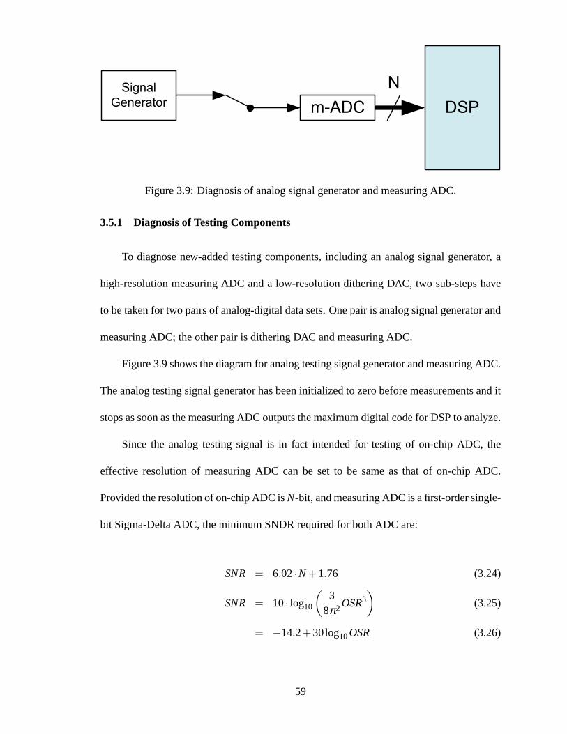
DSPm-ADC
Signal
Generator
N
Figure 3.9: Diagnosis of analog signal generator and measuring ADC.
3.5.1 Diagnosis of Testing Components
To diagnose new-added testing components, including an analog signal generator, a
high-resolution measuring ADC and a low-resolution dithering DAC, two sub-steps have
to be taken for two pairs of analog-digital data sets. One pair is analog signal generator and
measuring ADC; the other pair is dithering DAC and measuring ADC.
Figure 3.9 shows the diagram for analog testing signal generator and measuring ADC.
The analog testing signal generator has been initialized tozero before measurements and it
stops as soon as the measuring ADC outputs the maximum digital code for DSP to analyze.
Since the analog testing signal is in fact intended for testing of on-chip ADC, the
effective resolution of measuring ADC can be set to be same asthat of on-chip ADC.
Provided the resolution of on-chip ADC isN-bit, and measuring ADC is a first-order single-
bit Sigma-Delta ADC, the minimum SNDR required for both ADC are:
SNR = 6.02·N+1.76 (3.24)
SNR = 10· log10
(
38π2OSR3
)
(3.25)
= −14.2+30log10OSR (3.26)
59
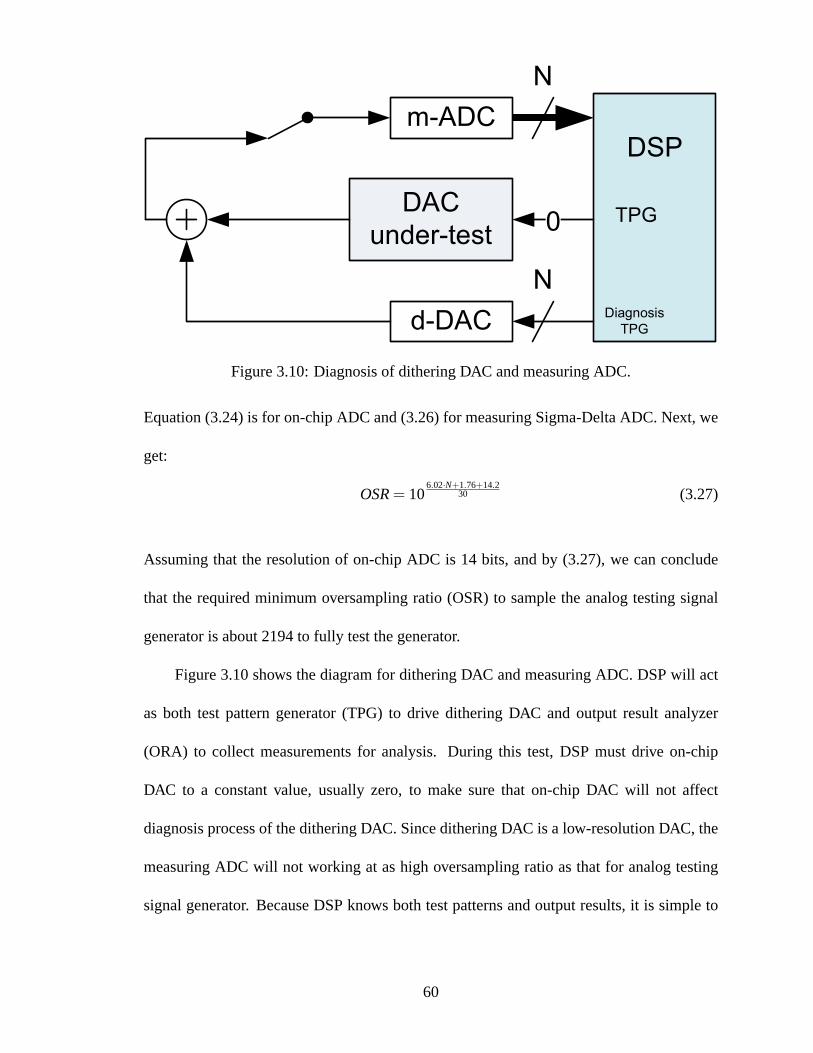
DAC
under-test
m-ADC
d-DAC
0
N
NDiagnosis
TPG
TPG
DSP
Figure 3.10: Diagnosis of dithering DAC and measuring ADC.
Equation (3.24) is for on-chip ADC and (3.26) for measuring Sigma-Delta ADC. Next, we
get:
OSR= 106.02·N+1.76+14.2
30 (3.27)
Assuming that the resolution of on-chip ADC is 14 bits, and by(3.27), we can conclude
that the required minimum oversampling ratio (OSR) to samplethe analog testing signal
generator is about 2194 to fully test the generator.
Figure 3.10 shows the diagram for dithering DAC and measuring ADC. DSP will act
as both test pattern generator (TPG) to drive dithering DAC and output result analyzer
(ORA) to collect measurements for analysis. During this test, DSP must drive on-chip
DAC to a constant value, usually zero, to make sure that on-chip DAC will not affect
diagnosis process of the dithering DAC. Since dithering DAC is a low-resolution DAC, the
measuring ADC will not working at as high oversampling ratioas that for analog testing
signal generator. Because DSP knows both test patterns and output results, it is simple to
60
detect any inconsistence between these two digital values and find possible errors in the
dithering DAC.
Assuming that the resolution of the dithering DAC is only 6 bits, apply it to the same
equation (3.27), then we can get the minimum OSR for this caseis 55. Therefore the
diagnosis of dithering DAC is much faster than that of analogsignal generator.
If both self-diagnoses pass the test by demonstrating desired form of digital signals,
for example, rising digital consecutive codes for linear ramp signals, we can consider the
newly-added testing hardware without fault. There could beonly one exceptional case that
existing fault cannot be detected, which happens when analog testing signals and dithering
DAC has the exactly same nonlinearity errors and those errors can exactly compensate those
of measuring ADC. It is obvious that such chance is very rare and it is nearly impossible
for all three components match the condition at the same time.
3.5.2 Test of On-Chip ADC
The proposed approach is shown in Figure 3.11 [27]. Similar to a histogram test-
ing method [56], this ADC BIST architecture also consists of three major components, a
test signal generator, the on-chip ADC under test and a digital signal processor (DSP) for
measured data processing and analysis.
Linear ramp testing signals are used to stimulate the ADC under test for simple im-
plementation and short test time. Let the linear ramp signals sampled by the on-chip ADC
be,
f (k) = a·T ·k+b (3.28)
61
RAMPADC
under test DSP
BIST CONTROL
Analog input
N
Figure 3.11: The proposed ADC BIST architecture.
whereT is interval time between samples,a andb are coefficients of the linear function
(a> 0), andk is the variable of samples.
Initially, b is presumed to be close enough to zero so that the measurements always
begin with code 0. This condition can be satisfied by the implementation to always reset
ramp signal generator to output signal close to zero. If the next sample is still measured
as 0 then the previous sample is discarded until a non-zero output code is measured. On
subsequent samples the output ascends until the measurement of K-th sample outputf (K)
reaches 2N −1 which is the maximum possible output code ofN-bit ADC. Thus, we have
following assumptions for the measured outputs of the ADC under test,
M(k)|k=0..K =
0 k= 0
MADC( f (k)) k= 1..K−1
2N −1 k= K
(3.29)
For an ideal ADC there is no nonlinearity error and the ramp testing signals may be recon-
structed using,
f (k)≈ M(k) ·LSB+eq (3.30)
62
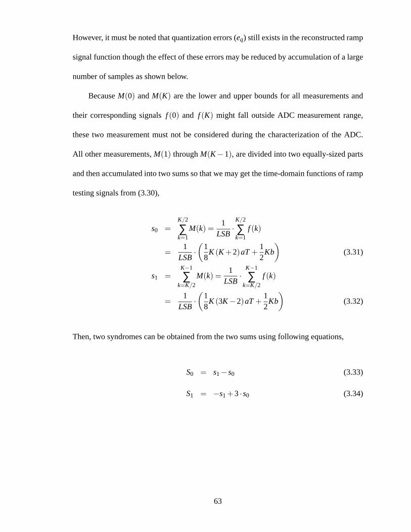
However, it must be noted that quantization errors (eq) still exists in the reconstructed ramp
signal function though the effect of these errors may be reduced by accumulation of a large
number of samples as shown below.
BecauseM(0) andM(K) are the lower and upper bounds for all measurements and
their corresponding signalsf (0) and f (K) might fall outside ADC measurement range,
these two measurement must not be considered during the characterization of the ADC.
All other measurements,M(1) throughM(K −1), are divided into two equally-sized parts
and then accumulated into two sums so that we may get the time-domain functions of ramp
testing signals from (3.30),
s0 =K/2
∑k=1
M(k) =1
LSB·
K/2
∑k=1
f (k)
=1
LSB·(
18
K (K+2)aT+12
Kb
)
(3.31)
s1 =K−1
∑k=K/2
M(k) =1
LSB·
K−1
∑k=K/2
f (k)
=1
LSB·(
18
K (3K−2)aT+12
Kb
)
(3.32)
Then, two syndromes can be obtained from the two sums using following equations,
S0 = s1−s0 (3.33)
S1 = −s1+3·s0 (3.34)
63
Applying (3.31) and (3.32) to (3.33) and (3.34), respectively, we get
S0 =1
LSB·(
14
K (K−2)aT
)
(3.35)
S1 =1
LSB· (K (aT+b)) (3.36)
From these two equations, the coefficients of the ramp signalfunction can be found as,
a = LSB· 4S0
K (K−2)· 1T
(3.37)
b = LSB·(
S1K−2S1−4S0
K (K−2)
)
(3.38)
Finally, the two coefficients of time-domain ramp function (3.28) can be recovered from
two sums by applying (3.33) and (3.34). Thus,
a = LSB· 4(s1−s0)K (K−2)
· 1T
(3.39)
b = LSB· (3s0−s1)K−2(s0+s1)
K (K−2)(3.40)
A DSP block, presumed to be available on the mixed-signal SoC,is used to accomplish
all computations shown above. The on-chip ADC measures testsignals and the DSP reads
and processes the ADC output codes. It uses (3.39) and (3.40)to approximately reconstruct
the original ramp test signal function. The DSP then compares each ADC measurement to
the expected code from the reconstructed test signal function to get INL errors of the ADC
under test. The two coefficients can also be used to determineoffset errors of the ADC
under test.
64

The principal steps of the proposed BIST approach for on-chipADC can be described
as follows [27]:
1. Reset testing signal generator to output ramp signals.
2. Detect first non-zero output from ADC; all previous samplesare discarded.
3. Measure all subsequent samples and record ADC output codes until the maximum
possible code are detected.
4. Accumulate measured samples in two equally divided partsand get two sums.
5. Using (3.39) and (3.40) obtain approximate coefficients for the signal function.
6. Calculate expected code for each sample using the obtainedsignal function and com-
pare it to the measured code to get INL errors.
The two coefficients of the test signal function can also be used for a preliminary esti-
mation of INL error of the ADC under test. The absolute value of magnitude of coefficient
b indicates overall offset error of ADC and the value ofa indicates ramp slope of testing
signals. The coefficientb should be around zero because‖b‖ < 0.5LSB, anda should be
close to the design specification of ramp signal generator for ADC under test to pass BIST.
If the preliminary conditions are not satisfied, there will be a high probability that that ADC
under test is faulty.
The same idea can also be applied when using low-frequency sinusoidal test signals
for nonlinearity test of an ADC under test. Let a sinusoidal test signal be in the form shown
below:
f (k) = A
[
1+sin
(
ωT ·k− pi2
)]
(3.41)
65
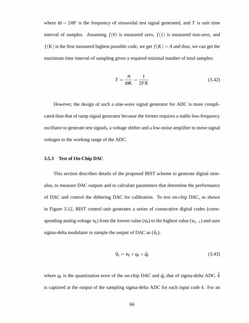
whereω = 2πF is the frequency of sinusoidal test signal generated, andT is unit time
interval of samples. Assumingf (0) is measured zero,f (1) is measured non-zero, and
f (K) is the first measured highest possible code, we getf (K) = A and thus, we can get the
maximum time interval of sampling given a required minimal number of total samples:
T =π
ωK=
12FK
(3.42)
However, the design of such a sine-wave signal generator forADC is more compli-
cated than that of ramp signal generator because the former requires a stable low-frequency
oscillator to generate test signals, a voltage shifter and alow-noise amplifier to move signal
voltages to the working range of the ADC.
3.5.3 Test of On-Chip DAC
This section describes details of the proposed BIST scheme togenerate digital stim-
ulus, to measure DAC outputs and to calculate parameters that determine the performance
of DAC and control the dithering DAC for calibration. To teston-chip DAC, as shown
in Figure 3.12, BIST control unit generates a series of consecutive digital codes (corre-
sponding analog voltageνk) from the lowest value (ν0) to the highest value (νn−1) and uses
sigma-delta modulator to sample the output of DAC as (νk):
νk = νk+qk+ qk (3.43)
whereqk is the quantization error of the on-chip DAC and ˆqk that of sigma-delta ADC.k
is captured at the output of the sampling sigma-delta ADC foreach input codek. For an
66
Sigma−Delta Modulator
LPF digita l
filter
DACunder−test
BIST CONTROL
UNIT
Figure 3.12: Test circuitry of DAC.
accurate measurement,k must contain more effective number of bits (ENOB) than that in
k. The ENOB ofk is determined by the oversampling ratioK, and requires higherK to
obtain larger ENOB and better resolution. Thus, the total quantization error for each code
k is,
εk = νk−νk = qk+ qk (3.44)
qk is small enough to be ignored with high oversampling ratioK and thus the quantization
error is mainly from the on-chip DAC. The dithering DAC will then eliminateεk from the
DAC output for normal operation and output linearity can be further improved by employ-
ing a dynamic element mismatching (DEM) technique. Because of large number ofεk for
each codek, (2N in total for N-bit DAC), it requires a huge amount of memory to store
the compensation data for every code, thus the 3rd-order best fit algorithm shown above
is used to reduce memory consumption. On the other hand, the quantization errorεk for
each codek also satisfies the requirements for the polynomial fitting algorithm. Applying
67
the fitting algorithm toINL errorεk, rather than resultνk obtained from sigma-delta mod-
ulator as [23] proposed, will make it easier for dithering DAC to generate compensation
signals. The consecutive codes fromν0 to νn−1 are divided into four equal-size segments
and quantization errorsεk in each segment are summed up to get four fundamental sum
values:
S0 =n/4−1
∑k=0
εk =n/4−1
∑k=0
(νk−νk) (3.45)
S1 =n/2−1
∑k=n/4
εk =n/2−1
∑k=n/4
(νk−νk) (3.46)
S2 =3n/4−1
∑k=n/2
εk =3n/4−1
∑k=n/2
(νk−νk) (3.47)
S3 =n−1
∑k=3n/4
εk =n−1
∑k=3n/4
(νk−νk) (3.48)
wheren= 2N is the total value range for theN-bit on-chip DAC.
Being mathematically equivalent to the least-square fit it can produce the best unbiased
(linear) estimates for the coefficients by feeding converter with a linear ramp test stimulus
covering the full range of conversion. The converter may work at full speed to traverse the
ramp stimulus and the output results are sampled by a measuring device. The full range
of conversion is divided into four equal interval segments,as shown in Figure 5.1. The
samples at each segment are accumulated and the four sums areS0, S1, S2, andS3. The
general third-order polynomial equation to fit converters is
y= b0+b1x+b2x2+b3x3 (3.49)
68
The inputx is assumed to be a cosine waveform to relate the four coefficients to harmonic
distortion,
x= A·cos(ωt) (3.50)
y= c0+c1cos(ωt)+c2cos(2ωt)+c3cos(3ωt) (3.51)
wherec0, c1, c2, andc3 represent DC offset, gain, and 2nd and 3rd harmonic distortions,
respectively.
We assume the following four syndromes from combination of sums:
B0 = S3+S2+S1+S0 (3.52)
B1 = S3+S2−S1−S0 (3.53)
B2 = S3−S2−S1+S0 (3.54)
B3 = S3−3S2+3S1−S0 (3.55)
One can derive [23] four coefficients for the best fit polynomial from the syndromes:
b0 =1N
(
B0−43
B2
)
(3.56)
b1 =4
N ·n
(
B1−43
B3
)
(3.57)
b2 =16
N ·n2 ·B2 (3.58)
b3 =128
3·N ·n3 ·B3 (3.59)
69
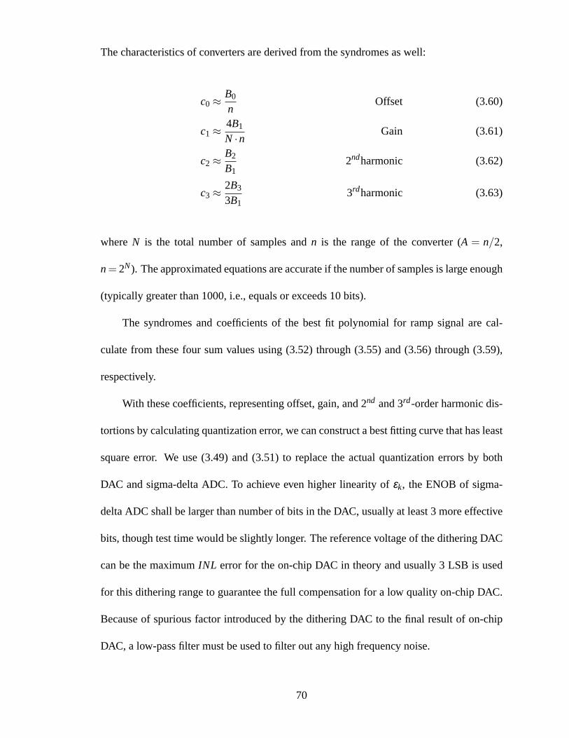
The characteristics of converters are derived from the syndromes as well:
c0 ≈B0
nOffset (3.60)
c1 ≈4B1
N ·n Gain (3.61)
c2 ≈B2
B12ndharmonic (3.62)
c3 ≈2B3
3B13rdharmonic (3.63)
whereN is the total number of samples andn is the range of the converter (A = n/2,
n= 2N). The approximated equations are accurate if the number of samples is large enough
(typically greater than 1000, i.e., equals or exceeds 10 bits).
The syndromes and coefficients of the best fit polynomial for ramp signal are cal-
culate from these four sum values using (3.52) through (3.55) and (3.56) through (3.59),
respectively.
With these coefficients, representing offset, gain, and 2nd and 3rd-order harmonic dis-
tortions by calculating quantization error, we can construct a best fitting curve that has least
square error. We use (3.49) and (3.51) to replace the actual quantization errors by both
DAC and sigma-delta ADC. To achieve even higher linearity ofεk, the ENOB of sigma-
delta ADC shall be larger than number of bits in the DAC, usually at least 3 more effective
bits, though test time would be slightly longer. The reference voltage of the dithering DAC
can be the maximumINL error for the on-chip DAC in theory and usually 3 LSB is used
for this dithering range to guarantee the full compensationfor a low quality on-chip DAC.
Because of spurious factor introduced by the dithering DAC tothe final result of on-chip
DAC, a low-pass filter must be used to filter out any high frequency noise.
70
3.5.4 Calibration of On-Chip ADC/DAC
After coefficients of the fitting polynomial are obtained from syndromes, the poly-
nomial can be used to recover static INL error for each code and therefore can be used to
drive dithering-DAC to generate compensating signals to fixnonlinear quantization outputs
of on-chip DAC.
To calibrate on-chip DAC, the quantization error of DAC can becalculated by two
output values,
∆νk = νk− νk (3.64)
for each test stimulus codek, whereνk is the ideal DAC output andνk is the actual output of
DAC-under-test. Four coefficients of a 3rd-order polynomial function are calculated from
the sums obtained from four equally-divided segments.∆k is theN′-bit code of calculated
voltage value∆νk by N-bit codek and N-bit code k. ∆k will be used by digital BIST
control unit for actual calculation to obtain coefficients.These four coefficients will be
used to recoverN′-bit code∆k, to generate compensation signal for DAC output during
ADC BIST in next step, and in the normal operation until the power is finally turned off.
An N′-bit dithering DAC using a dynamic element matching (DEM) technique is used
for accurate compensation with high-tolerance mismatchesamong the current sources of
the DAC. Assuming DEM iteration factorp, meaningN′-bit dithering DAC generatesp
outputs for each input code∆k, we get DEM elements distance factorq so thatp ·q= 2N′.
After eliminating spurious data by an LPF, the performance of dithering DEM DAC is
comparable to an ideal DAC withN′+ log2 p ENOB as discussed in a previous paper [57].
A typical implementation of dithering DEM DAC contains 2N′current sources which are
71
divided intop segments with element distance ofq. For any codek, k consecutive current
sources from(d−1)q+1 through(d−1)q+k are turned on atdth iteration (1≤ p).
The implementation of BIST circuitry and algorithm to test ADC-under-test is quite
similar to the techniques used for DAC-under-test. BIST control unit generates exactly the
same consecutive codes as digital test stimuli for the on-chip DAC, which then outputs an
analog ramp signal. BIST reads the digital conversion outputof ADC-under-test whose
input is the ramp signal. Since testing and calibration of DAC has been completed in the
previous step and the resolution and linearity is improved,the quantization error of DAC
may be ignored now.
Four coefficients of a third-order best-fitting polynomial function are obtained from
the output of ADC in a similar fashion as was done for the Sigma-Delta modulator in the
previous step. The calibration of on-chip ADC is simple,
k= k′+∆k (3.65)
wherek′ is N′-bit ADC output,∆k is calculated from polynomial function, andk is cali-
brated result. We should point out that this procedure only makes limited compensation to
the linearity and does not improve the resolution of ADC-under-test.
The proposed test and calibration approach is verified by simulation in Matlab for 14-
bit on-chip DAC and ADC model on various quantization noise levels. A 6-bit low-cost
dithering DAC model is used in the simulation to generate compensating analog signal
for DAC calibration. The reference voltage for the dithering DAC is 3 LSB of on-chip
72
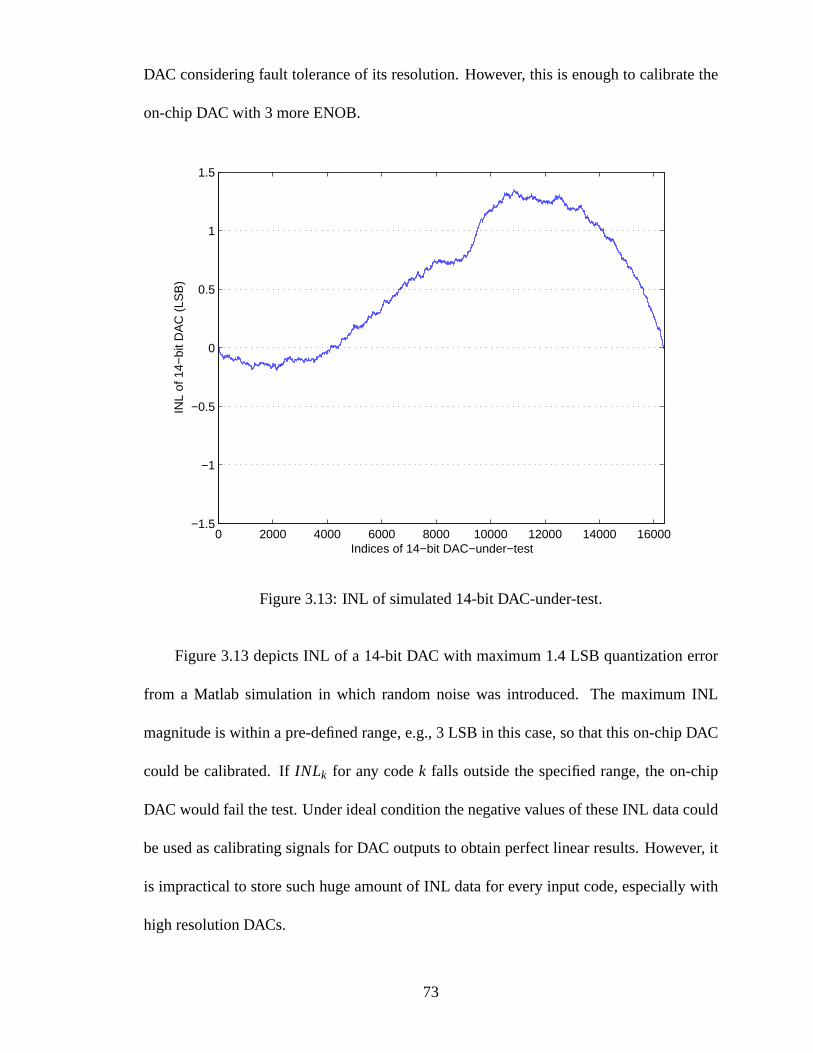
DAC considering fault tolerance of its resolution. However, this is enough to calibrate the
on-chip DAC with 3 more ENOB.
0 2000 4000 6000 8000 10000 12000 14000 16000−1.5
−1
−0.5
0
0.5
1
1.5
Indices of 14−bit DAC−under−test
INL
of 1
4−bi
t DA
C (
LSB
)
Figure 3.13: INL of simulated 14-bit DAC-under-test.
Figure 3.13 depicts INL of a 14-bit DAC with maximum 1.4 LSB quantization error
from a Matlab simulation in which random noise was introduced. The maximum INL
magnitude is within a pre-defined range, e.g., 3 LSB in this case, so that this on-chip DAC
could be calibrated. IfINLk for any codek falls outside the specified range, the on-chip
DAC would fail the test. Under ideal condition the negative values of these INL data could
be used as calibrating signals for DAC outputs to obtain perfect linear results. However, it
is impractical to store such huge amount of INL data for everyinput code, especially with
high resolution DACs.
73
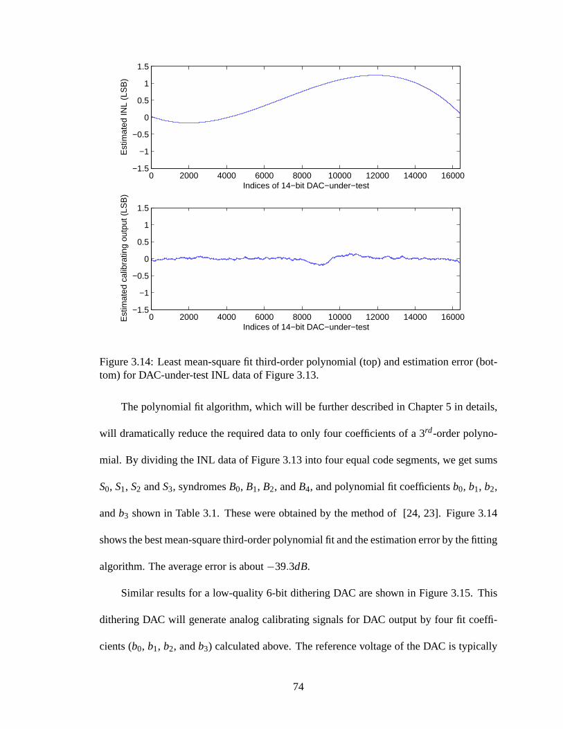
0 2000 4000 6000 8000 10000 12000 14000 16000−1.5
−1
−0.5
0
0.5
1
1.5
Indices of 14−bit DAC−under−test
Est
imat
ed IN
L (L
SB
)
0 2000 4000 6000 8000 10000 12000 14000 16000−1.5
−1
−0.5
0
0.5
1
1.5
Indices of 14−bit DAC−under−test
Est
imat
ed c
alib
ratin
g ou
tput
(LS
B)
Figure 3.14: Least mean-square fit third-order polynomial (top) and estimation error (bot-tom) for DAC-under-test INL data of Figure 3.13.
The polynomial fit algorithm, which will be further described in Chapter 5 in details,
will dramatically reduce the required data to only four coefficients of a 3rd-order polyno-
mial. By dividing the INL data of Figure 3.13 into four equal code segments, we get sums
S0, S1, S2 andS3, syndromesB0, B1, B2, andB4, and polynomial fit coefficientsb0, b1, b2,
andb3 shown in Table 3.1. These were obtained by the method of [24, 23]. Figure 3.14
shows the best mean-square third-order polynomial fit and the estimation error by the fitting
algorithm. The average error is about−39.3dB.
Similar results for a low-quality 6-bit dithering DAC are shown in Figure 3.15. This
dithering DAC will generate analog calibrating signals forDAC output by four fit coeffi-
cients (b0, b1, b2, andb3) calculated above. The reference voltage of the DAC is typically
74
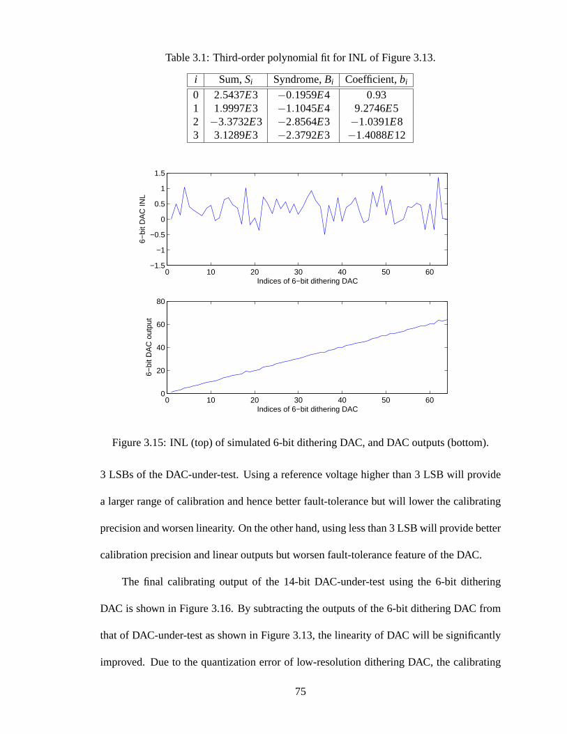
Table 3.1: Third-order polynomial fit for INL of Figure 3.13.
i Sum,Si Syndrome,Bi Coefficient,bi
0 2.5437E3 −0.1959E4 0.931 1.9997E3 −1.1045E4 9.2746E52 −3.3732E3 −2.8564E3 −1.0391E83 3.1289E3 −2.3792E3 −1.4088E12
0 10 20 30 40 50 60−1.5
−1
−0.5
0
0.5
1
1.5
Indices of 6−bit dithering DAC
6−bi
t DA
C IN
L
0 10 20 30 40 50 600
20
40
60
80
Indices of 6−bit dithering DAC
6−bi
t DA
C o
utpu
t
Figure 3.15: INL (top) of simulated 6-bit dithering DAC, and DAC outputs (bottom).
3 LSBs of the DAC-under-test. Using a reference voltage higherthan 3 LSB will provide
a larger range of calibration and hence better fault-tolerance but will lower the calibrating
precision and worsen linearity. On the other hand, using less than 3 LSB will provide better
calibration precision and linear outputs but worsen fault-tolerance feature of the DAC.
The final calibrating output of the 14-bit DAC-under-test using the 6-bit dithering
DAC is shown in Figure 3.16. By subtracting the outputs of the 6-bit dithering DAC from
that of DAC-under-test as shown in Figure 3.13, the linearityof DAC will be significantly
improved. Due to the quantization error of low-resolution dithering DAC, the calibrating
75
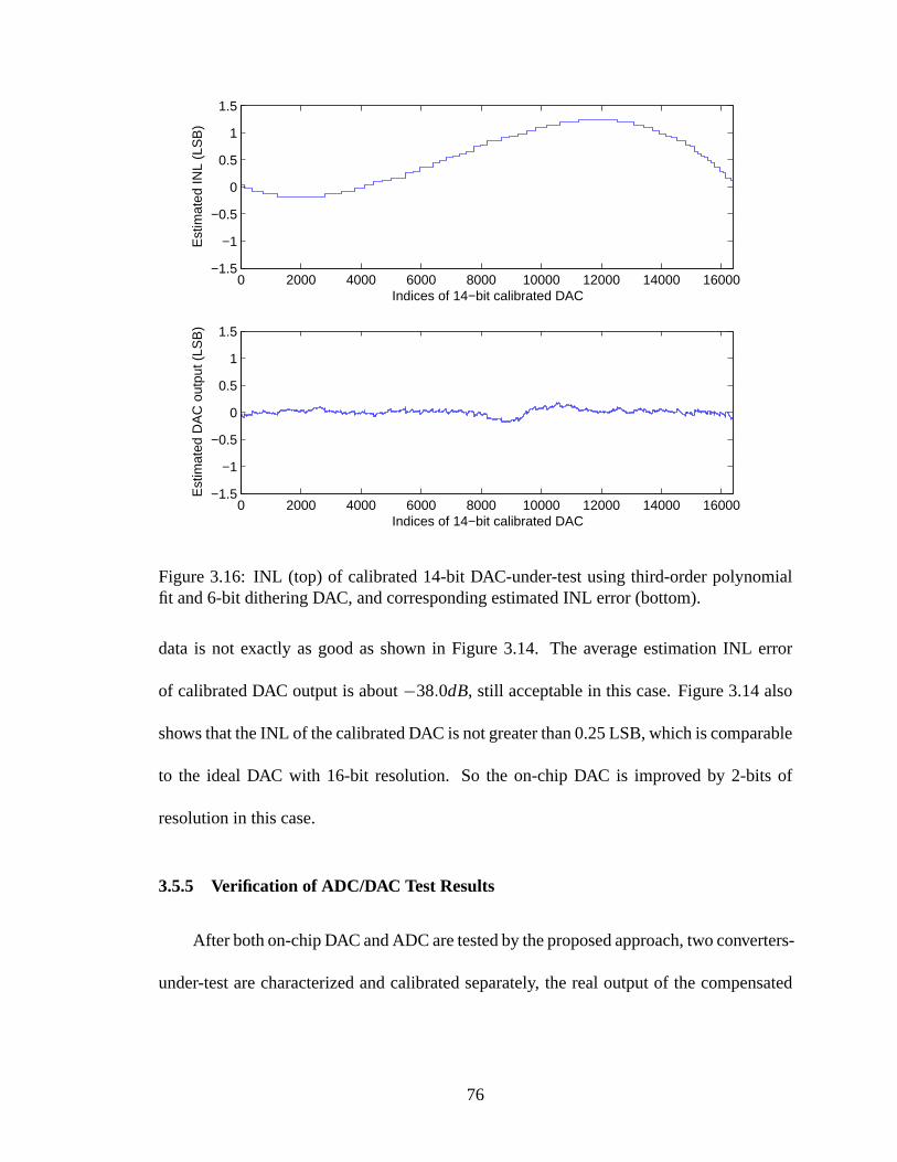
0 2000 4000 6000 8000 10000 12000 14000 16000−1.5
−1
−0.5
0
0.5
1
1.5
Indices of 14−bit calibrated DAC
Est
imat
ed IN
L (L
SB
)
0 2000 4000 6000 8000 10000 12000 14000 16000−1.5
−1
−0.5
0
0.5
1
1.5
Indices of 14−bit calibrated DAC
Est
imat
ed D
AC
out
put (
LSB
)
Figure 3.16: INL (top) of calibrated 14-bit DAC-under-test using third-order polynomialfit and 6-bit dithering DAC, and corresponding estimated INL error (bottom).
data is not exactly as good as shown in Figure 3.14. The average estimation INL error
of calibrated DAC output is about−38.0dB, still acceptable in this case. Figure 3.14 also
shows that the INL of the calibrated DAC is not greater than 0.25 LSB, which is comparable
to the ideal DAC with 16-bit resolution. So the on-chip DAC isimproved by 2-bits of
resolution in this case.
3.5.5 Verification of ADC/DAC Test Results
After both on-chip DAC and ADC are tested by the proposed approach, two converters-
under-test are characterized and calibrated separately, the real output of the compensated
76
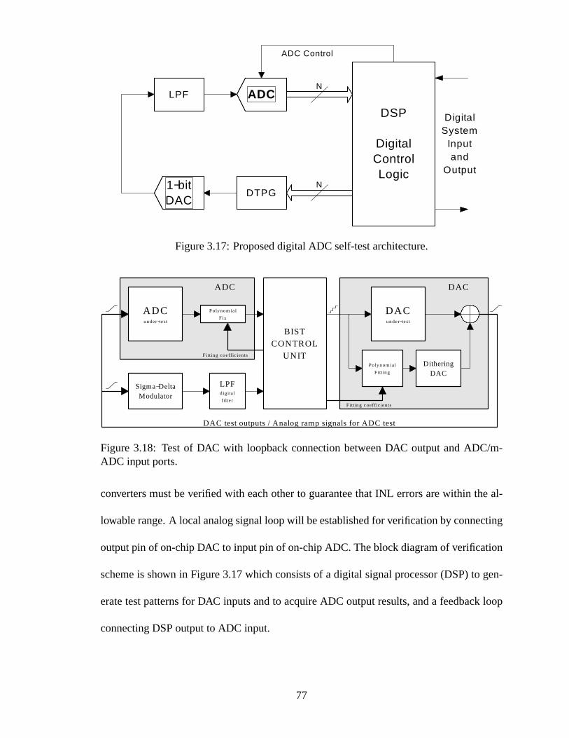
ADC
DSP
Digital Control Logic
Digital System
Input and
Output
ADC Control
DTPG
LPF
1−bit DAC
N
N
Figure 3.17: Proposed digital ADC self-test architecture.
Polynom ia l
F ixADCunder−test
Sigma−Delta Modulator
LPF d ig ita l
f ilte r
DACunder−test
Po lynom ia l
F itting
Dithering DAC
BIST CONTROL
UNITFitting coe ff ic ien ts
F itting coeff ic ien ts
DAC test outputs / Analog ramp signals for ADC test
ADC DAC
Figure 3.18: Test of DAC with loopback connection between DAC output and ADC/m-ADC input ports.
converters must be verified with each other to guarantee thatINL errors are within the al-
lowable range. A local analog signal loop will be established for verification by connecting
output pin of on-chip DAC to input pin of on-chip ADC. The blockdiagram of verification
scheme is shown in Figure 3.17 which consists of a digital signal processor (DSP) to gen-
erate test patterns for DAC inputs and to acquire ADC output results, and a feedback loop
connecting DSP output to ADC input.
77
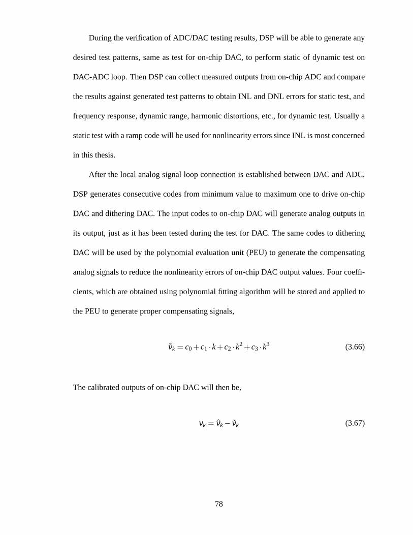
During the verification of ADC/DAC testing results, DSP will be able to generate any
desired test patterns, same as test for on-chip DAC, to perform static of dynamic test on
DAC-ADC loop. Then DSP can collect measured outputs from on-chip ADC and compare
the results against generated test patterns to obtain INL and DNL errors for static test, and
frequency response, dynamic range, harmonic distortions,etc., for dynamic test. Usually a
static test with a ramp code will be used for nonlinearity errors since INL is most concerned
in this thesis.
After the local analog signal loop connection is established between DAC and ADC,
DSP generates consecutive codes from minimum value to maximum one to drive on-chip
DAC and dithering DAC. The input codes to on-chip DAC will generate analog outputs in
its output, just as it has been tested during the test for DAC. The same codes to dithering
DAC will be used by the polynomial evaluation unit (PEU) to generate the compensating
analog signals to reduce the nonlinearity errors of on-chipDAC output values. Four coeffi-
cients, which are obtained using polynomial fitting algorithm will be stored and applied to
the PEU to generate proper compensating signals,
νk = c0+c1 ·k+c2 ·k2+c3 ·k3 (3.66)
The calibrated outputs of on-chip DAC will then be,
νk = νk− νk (3.67)
78
The combined analog signals of on-chip DAC and dithering DACthen will be mea-
sured by on-chip ADC and subsequently retrieved by DSP for comparison against the cor-
responding generated test patterns. If the verification step confirms that nonlinearity errors
between generated test patterns and measured samples are within 0.5LSB, it means that
both on-chip DAC and ADC are both operating normal after calibration because in the
previous steps they are independently tested and calibrated. Otherwise, either one of on-
chip DAC or ADC may be faulty if in the verification steps any nonlinearity error is found
exceed 0.5LSB.
3.5.6 Minimal Number of Samples
Since measurements by ADC always contain quantization errors owing to its nature
to convert continuous analog wave into discrete digital code, a minimal number of samples
must be taken to ensure that such quantization errors are negligible in the process. Let us
first consider an ideal ADC. The quantization errors of the ideal ADC can be anywhere
between±LSB2 , and as more samples ADC measures less quantization errors remain after
accumulating all measurements. A histogram approach can beconsidered as the extreme
situation of the requirements, which needs multiple samples for each code to make sure
that the quantization error is essentially removed from statistical distribution of codes.
However, for a non-ideal ADC under test, there are two possibilities that must be taken
into consideration. It is always possible that some codes with greater nonlinearity errors
are not measured during BIST, and also it is possible that a measured nonlinearity error
introduces distortion to the reconstructed transfer function of ramp signals.
79
Generally, the first problem will be non-existent if every code is measured at least
once, and the second problem will be effectively eliminatedwith large number of samples
because such nonlinearity errors will be attenuated to makelittle impact on the calculation.
In practice, we found that at least 2N−2 samples should be measured to perform this BIST
procedure on anN-bit ADC to avoid these two issues and ensure that ramp signals are
reconstructed properly.
3.5.7 Delay of Polynomial Evaluation
The other issue is the miscorrelation between delay times ofDAC-under-test and poly-
nomial evaluation unit. Since polynomial evaluation involves large amount polynomial
calculation, which is mostly digital circuits, it will impose additional delay from DSP to
dithering-DAC. Hence a potential issue arises to the calibrated DAC outputs because the
output analog signals could be divided into two sections. Inthe first section, on-chip DAC
generates output signals which possibly contain nonlinearity errors larger than 0.5LSB.
In the second section, dither-DAC generates compensating signals to fix corresponding
nonlinearity DAC outputs by removing portion of nonlinearities. However, due to the dif-
ferences in delay between these two timing paths, these two signals may not arrive at DAC
output simultaneously and therefore cause additional unexpected error to the analog sys-
tem. To diminish such delay effects, the combined delay of polynomial calculation circuitry
and low-resolution dithering-DAC must be less or equal to the conversion time of on-chip
DAC.
Thus, the delay of polynomial evaluation unit must be taken into consideration in
the late verification step. After DSP drive on-chip DSP and dithering-DSP with certain
80
test pattern, it will expect a measured data from on-chip ADCoutputs. If DSP observes
miscorrelation in the measurements, even the final measurements being correct and within
the 0.5LSB limit, the verification must show a failure.
3.6 Summary
In this chapter, the proposed built-in self-test and calibration scheme for analog-to-
digital and digital-to-analog converters is described in details. On-chip ADC is tested us-
ing ramp signals from analog signal generator, and its outputs are collected by DSP. On
the other side, On-chip DAC is tested by digital ramp test patterns generated by DSP, and
measured by a high-linearity measuring-ADC, which is based on Sigma-Delta modula-
tion. Both data from ADC and DAC are finally processed by DSP using polynomial fitting
algorithm to obtain four polynomial coefficients which can be used to estimate characteri-
zations of converters, such as offset, gain, and high order distortions. The four polynomial
coefficients then will be used by polynomial evaluation unitduring result verification and
normal operations. In the final result verification step, DSPwill generate another set of test
patterns, usually ramp patterns, to drive both on-chip DAC and dithering DAC (through
polynomial evaluation unit to calibrate DAC) to make DAC outputs with reduced nonlin-
earity errors. On-chip ADC will measure the combined DAC outputs after calibration to
verify that nonlinearity errors of both DAC and ADC are within 0.5LSB. Otherwise, it
means that either the on-chip ADC or DAC is faulty.
81
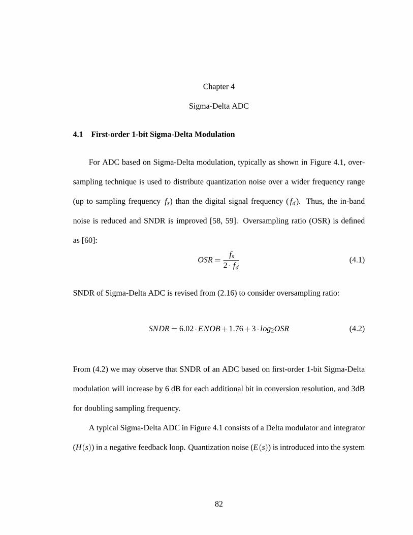
Chapter 4
Sigma-Delta ADC
4.1 First-order 1-bit Sigma-Delta Modulation
For ADC based on Sigma-Delta modulation, typically as shownin Figure 4.1, over-
sampling technique is used to distribute quantization noise over a wider frequency range
(up to sampling frequencyfs) than the digital signal frequency (fd). Thus, the in-band
noise is reduced and SNDR is improved [58, 59]. Oversamplingratio (OSR) is defined
as [60]:
OSR=fs
2· fd(4.1)
SNDR of Sigma-Delta ADC is revised from (2.16) to consider oversampling ratio:
SNDR= 6.02·ENOB+1.76+3· log2OSR (4.2)
From (4.2) we may observe that SNDR of an ADC based on first-order 1-bit Sigma-Delta
modulation will increase by 6 dB for each additional bit in conversion resolution, and 3dB
for doubling sampling frequency.
A typical Sigma-Delta ADC in Figure 4.1 consists of a Delta modulator and integrator
(H(s)) in a negative feedback loop. Quantization noise (E(s)) is introduced into the system
82
S
1−bit DAC
intergrator
y(t)
quantiztion
x(t)
e(t)
Z−1 Y(z)X(z)
E(z)
1−bit first−order Sigma−delta Modulator
Transfer function in z−domain
Figure 4.1: Schematic of an typical ADC based on first-order 1-bit Sigma-Delta modulationand its transfer function inz-domain.
by the quantizer (1-bit ADC) and a 1-bit DAC. The transfer function of close loop of Sigma-
Delta modulator can shape the quantization noise by pushingthe noise further up to out-
band of input signal, so that a low-pass filter (typically digital filter, e.g., accumulator) will
be able to remove the most of noise. Let input and output signals of the Sigma-Delta ADC
in s-domain beX(s) andY(s), respectively.
Y(s) = X(s) · H(s)1+H(s)
+E(s) · 11+H(s)
(4.3)
83
It can be observed that the close loop acts like a low-pass filter for input signal (X(s))
and high-pass filter for quantization noise (E(s)). Due to 1-bit ADC and DAC used in
the negative feedback loop, nonlinearity error in these analog components can be ignored.
Therefor with oversampling and noise shaping techniques, Sigma-Delta ADC is able to
achieve both high resolution and high linearity with large number of OSR.
However, according to the Nyquist-Shannon sampling theorem, given a specific sam-
pling frequency, large OSR will effectively reduce bandwidth of input signal and also extent
the conversion time. Conversion time is also a critical measurement of ADC performance,
especially for high speed applications which require fast converting rate for high frequency
input analog signals.
The digital BIST circuitry cannot process the analog ramp signals directly, so we
employ a first-order 1-bit Sigma-Delta modulator to sample DAC output and to convert
each analog signalk to corresponding digital codek.
The proposed Sigma-Delta modulator includes an integrator, an 1-bit quantizer, and an
1-bit DAC. With oversampling and noise-shaping techniques Sigma-Delta DAC is simple
to design and implement for achieving high linearity without strict requirements for high
quality components. By oversampling the quantization noiseof Sigma-Delta ADC is uni-
formly distributed over a wider band up to half of sampling frequency (Nyquist frequency)
and therefore the overall noise figure is reduced. Because thesignal to noise ratio (SNR) of
simple oversampling increases by 3dB for each doubled sampling rate, the oversampling
rate (OSR) must be quadrupled for each ENOB of resolution gain. The feedback loop
(consisting of a quantizer and a 1-bit DAC) acts as a low-pass filter for input analog signals
and high-pass filter for internal quantization error. So thequantization noise is removed
84
from the lower band and is concentrated in the high-frequency end of the Nyquist band.
Therefore, the noise is shaped to higher band than input signals.
More than one integration and loop stages could be used to build high-order Sigma-
Delta modulators for better quantization noise-shaping and ENOB gain for a given OSR.
However, a high-order Sigma-Delta modulator is not as stable and linear as a first-order
modulator [61], which is our choice in this application. Testing time of the first-order 1-bit
Sigma-Delta modulator is not an issue since the testing and calibration procedure is exe-
cuted only during chip powering up and therefore modulator will not affect the performance
of the normal operation.
Figure 4.1 shows a typical design of first-order 1-bit Sigma-Delta modulator. The
transfer function of the modulator is
Y(z) = z−1X(z)+(1−z−1)E(z) (4.4)
whereE(z) is the quantization error introduced by the Sigma-Delta modulator.
Assuming oversampling rate of a Sigma-Delta modulator isM, each analog signal
output by DAC-under-test for codek must haveM samples by the modulator. The SNR of
Sigma-Delta modulator with an oversampling rateM is
M =fsf0
(4.5)
n0 = ermsπ√3
(
1M
)3/2
(4.6)
SNR=1
n0 ·2√
2(4.7)
≈√
3M3/2
2√
2π2(4.8)
85
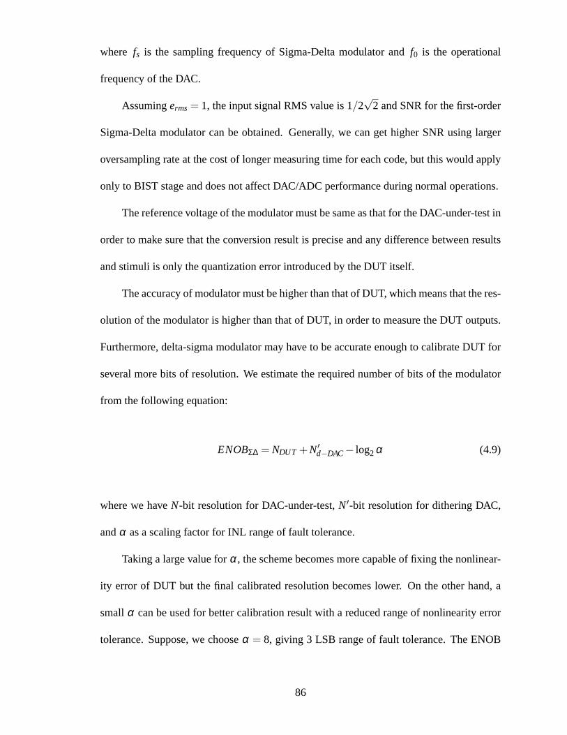
where fs is the sampling frequency of Sigma-Delta modulator andf0 is the operational
frequency of the DAC.
Assumingerms= 1, the input signal RMS value is 1/2√
2 and SNR for the first-order
Sigma-Delta modulator can be obtained. Generally, we can get higher SNR using larger
oversampling rate at the cost of longer measuring time for each code, but this would apply
only to BIST stage and does not affect DAC/ADC performance during normal operations.
The reference voltage of the modulator must be same as that for the DAC-under-test in
order to make sure that the conversion result is precise and any difference between results
and stimuli is only the quantization error introduced by theDUT itself.
The accuracy of modulator must be higher than that of DUT, which means that the res-
olution of the modulator is higher than that of DUT, in order to measure the DUT outputs.
Furthermore, delta-sigma modulator may have to be accurateenough to calibrate DUT for
several more bits of resolution. We estimate the required number of bits of the modulator
from the following equation:
ENOBΣ∆ = NDUT +N′d−DAC− log2α (4.9)
where we haveN-bit resolution for DAC-under-test,N′-bit resolution for dithering DAC,
andα as a scaling factor for INL range of fault tolerance.
Taking a large value forα, the scheme becomes more capable of fixing the nonlinear-
ity error of DUT but the final calibrated resolution becomes lower. On the other hand, a
smallα can be used for better calibration result with a reduced range of nonlinearity error
tolerance. Suppose, we chooseα = 8, giving 3 LSB range of fault tolerance. The ENOB
86
������������������������������������������������������������������������������������������������������������������������������������������������������
������������������������������������������������������������������������������������������������������������������������������������������������������
Quantization noise
Ou
tpu
t
fin fs/2
H(s)
sf6
2∆
Oversampling without feedback
Figure 4.2: Oversampling system without noise-shaping feedback.
of the modulator must be larger thanN = N+N′− 3 for the desired INL voltage range.
Thus, the SNR of the Sigma-Delta modulator is [62]
SNR= 6.02N+1.76 (4.10)
whereN is ENOB of the modulator calculated above for given DUT and dithering DAC.
4.1.1 Oversampling and Noise Shaping Techniques
From (4.2), we can find that the SNR improves by 6 dB for every bit added to the
quantizer. For the same amount of total quantization noise power, every doubling of the
sampling frequency reduces the in-band quantization noiseby 3 dB, as shown in Figure 4.2.
Thus RMS (root mean square) value of the in-band quantizationnoise is reduced by the
oversampling technique since the total noise is spread across the entire sampling band-
width [4]. Hence, every doubling the oversampling ratio (OSR) is equivalent to increasing
the quantizer levels by a half-bit for concerned quantization noise.
87
Oversampling technique allows the use of a lower-resolution converter without sac-
rificing noise performance and the trade-off between measuring time and accuracy. Dou-
bling the oversampling rate, meaning longer conversion time and lower converting signal
frequency at the same sampling frequency, gives two times number of correlated signal
samples and the signal power is increased by 6 dB. In other words, the signal samples are
correlated while the noise samples are not. Thus the SNR improvement of 3 dB is obtained
corresponding to a half-bit resolution improvement.
The benefit of oversampling technique is that the requirements on analog antialiasing
filter for A/D converters ordeglitchingfilters for D/A converters is lower due to wider
transition bands from oversampling and therefore only low-order filter are needed. The
disadvantage of oversampling technique is the requirements on high oversampling ratio to
achieve high resolution, that is, much higher sampling rates than ordinary A/D and higher
clock speed for digital circuits. It also means that the signal bandwidth sampled using
oversampling technique has to be much lower than sampling rate.
While oversampling technique is able to reduce the random quantization by averaging
such noise over a much wider sampling bandwidth due to high oversampling ratio, another
useful scheme for quantization noise reduction is noise shaping using negative feedback.
Considering the transfer function of first-order Sigma-Delta modulator (Figure 4.1) in (4.4),
a negative feedback is added to stabilize the system containing an integrator.
For in-band signalX(z), the system acts as a low-pass filter and the signal transfer
function is nearly unity at low frequencies. Similarly noise signalE(z) is approximately
zero for low frequencies due to its noise transfer function is like a high-pass filter. Thus
for the Sigma-Delta modulator, it is designed to have high gain for in-band signal in low
88
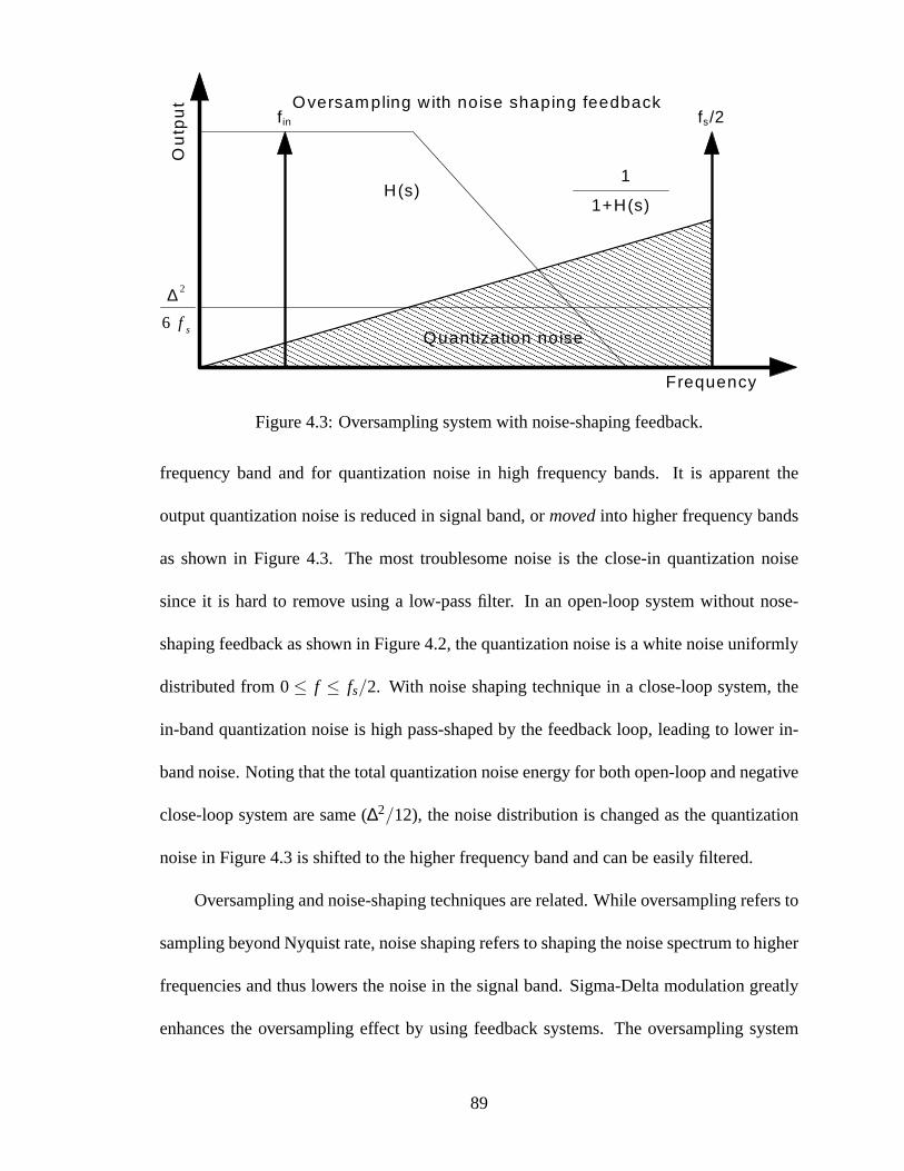
����������������������������������������������������������������������������������������������������������������������������������������������������������������������������������������������������������������������������������������������������������������������������������������������������������������������������������������������������������������������������������������������������������������
����������������������������������������������������������������������������������������������������������������������������������������������������������������������������������������������������������������������������������������������������������������������������������������������������������������������������������������������������������������������������������������������������������������
Ou
tpu
t
F requency
fin fs/2
H(s)
sf6
2∆
Quantization noise
Oversampling w ith noise shaping feedback
1+H(s)
1
Figure 4.3: Oversampling system with noise-shaping feedback.
frequency band and for quantization noise in high frequencybands. It is apparent the
output quantization noise is reduced in signal band, ormovedinto higher frequency bands
as shown in Figure 4.3. The most troublesome noise is the close-in quantization noise
since it is hard to remove using a low-pass filter. In an open-loop system without nose-
shaping feedback as shown in Figure 4.2, the quantization noise is a white noise uniformly
distributed from 0≤ f ≤ fs/2. With noise shaping technique in a close-loop system, the
in-band quantization noise is high pass-shaped by the feedback loop, leading to lower in-
band noise. Noting that the total quantization noise energyfor both open-loop and negative
close-loop system are same (∆2/12), the noise distribution is changed as the quantization
noise in Figure 4.3 is shifted to the higher frequency band and can be easily filtered.
Oversampling and noise-shaping techniques are related. While oversampling refers to
sampling beyond Nyquist rate, noise shaping refers to shaping the noise spectrum to higher
frequencies and thus lowers the noise in the signal band. Sigma-Delta modulation greatly
enhances the oversampling effect by using feedback systems. The oversampling system
89
with Sigma-Delta modulation is often called a high-order oversampling system since the
conventional oversampling system without Sigma-Delta modulation is, in fact, a zero-order
feedback system [4].
4.2 Digital Filter
The output of Sigma-Delta modulator is a bit stream of ‘0’ or ‘1’ which contains high-
frequency noise and cannot be directly processed by BIST control unit. A low-pass digital
filter (LPF) is required to filter out the noise. We use a simpleintegrator at the output of
Sigma-Delta modulator as LPF. It has been shown [33] that thez-domain transfer function
of a modulator and integrator is given by,
Y(z) =z−1
1−z−1X(z)+E(z) (4.11)
whereX(z) is Sigma-Delta input,Y(z) is the integrator output andE(z) is quantization
error. Thus, the input signal is recovered and quantizationerror is not accumulated, im-
proving the overall SNR. The final LPF output is then convertedto usual digital codek,
corresponding to input stimulusk plus quantization error from both DAC-under-test and
Sigma-Delta modulator.
Since the reference voltage is only about 3 LSB of DAC-under-test, the quantization
error of Sigma-Delta modulator is much less than that of DAC-under-test and therefore can
be ignored.
Since the oversampling technique distributes the overall quantization noise from band-
width of f0 to fs/2 by the oversampling ratiofs/ f0 and noise-shaping acts as a high-pass
90
filter for the quantization noise most which fall outside thesignal pass band, the digital
filter is actually a low-pass filter that eliminates the high frequency noise and keeps the low
frequency signals.
One simple method to implement the low-pass filter to extractsignals is to use an accu-
mulator that sums up the output bit-stream of the sigma-delta modulator. This accumulator
acts like a 1st−order low-pass filter with az-domain transfer function:
Y(z) =1
1−z−1Y(z) (4.12)
=z−1
1−z−1U(z)+E(z) (4.13)
Examining (4.13), we find that the signals in the bit-stream are extracted by the accumulator
and the high frequency noise shaped by sigma-delta modulator is very low in the band of
interest and therefore almost eliminated. The remaining noise in the accumulator output
is only due to the 1-bit quantization error (1 LSB) while the signal is reinforced during
accumulation to achieve much higher SNR.
The bit-stream generated by the sigma-delta modulator requires a smoothing process
calleddecimationthat eliminates redundant output data by down-sampling thebit-stream to
reconstruct the input signal without distortion. A down-sampling reduction ratioM means
that the sampling rate of the bit-stream is reduced by a factor M, equivalent to picking up
one of everyM samples from the stream to reconstruct the input signal and discard the
rest of the samples. No signal information will be lost during the down-sampling process
provided that decimation data rate is more than twice the signal band widthf0. Digital
filter using decimation will minimize the requirements for ahigh speed parallel multiplier
and a large memory to store every bit of the lengthy stream. A common implementation
91
of such decimation is comb filter, or sometimes calledsinc filter that will also eliminate
the unnecessary high frequency portions of the bit-stream.Onget al. [34] give an efficient
implementation of a comb filter by cascadingK stages of accumulators operating at the
sampling rate of the sigma-delta modulator, followed byK stages of cascaded differen-
tiators operating at the down-sampled rate. The transfer function of the sinc filter withK
stages and a down-sample ratioM has the form:
H(z) =
(
1M
1−z−M
1−z−1
)K
(4.14)
with a frequency response:
∣
∣H(
ejω)∣∣=
(
1M
sin(ωM/2)sin(ω/2)
)K
(4.15)
The desired frequency components should be contained within the first peak of the fre-
quency response. We also observe that largerK yields larger attenuation to frequency
response and largerM yields more and thinner peaks so properK andM should be chosen
carefully to filter the desired frequency components to reconstruct the signal.
4.3 Summary
In this chapter, a first-order 1-bit Sigma-Delta modulationis described and the over-
sampling and noise-shaping techniques are introduced. Because of its simple architecture
and high linearity, the Sigma-Delta modulator-based ADC ischosen as the best candi-
date for measuring-ADC, which requires low hardware overhead and higher linearity than
DAC-under-test. With oversampling technique, the measuring-ADC can achieve higher
92

resolution by using greater oversampling ratio (OSR), whichsacrificing conversion time
for higher SNR and therefore higher resolution. Since measuring-ADC is only employed
only once during testing steps and will be turned off after BIST and calibration steps fin-
ish, the conversion time is not a critical factor because it will not greatly impact overall
performance of the mixed-signal system.
93
Chapter 5
Polynomial Fitting Algorithm
5.1 Overview
As our research has shown [25, 26, 27], a simplified polynomial-fitting algorithm [23,
24] can be employed for characterizing DAC/ADC by four coefficients that form a best
fit 3rd-order polynomial curve for the transfer function of the converters. The input code
range of the DAC is divided into four equal segments as illustrated in Figure 5.1. For these
segments,S0, S1, S2 and S3 are the sums of outputs corresponding the included codes.
Syndromes,B0, B1, B2 andB3, are then obtained as specific linear combinations of the
sums, and these allow the computation of four coefficients,b0, b1, b2 andb3, for a least
mean-square fit of a third-order polynomial:
y(x) = b0+b1x+b2x2+b3x3 (5.1)
wherex is the input code andy(x) is the analog output of DAC.
5.2 Fitting Algorithm
This algorithm [23, 24] eliminates the requirement for massive amount memory to
store individual sampled data as some schemes using histogram algorithms do. We apply
this kind of third-order mean-square fit to the integral nonlinearity (INL) calculated as the
94
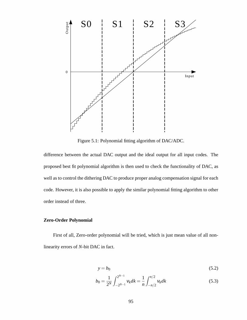
S0 S1 S2 S3
Input
Ou
tpu
t
0
Figure 5.1: Polynomial fitting algorithm of DAC/ADC.
difference between the actual DAC output and the ideal output for all input codes. The
proposed best fit polynomial algorithm is then used to check the functionality of DAC, as
well as to control the dithering DAC to produce proper analogcompensation signal for each
code. However, it is also possible to apply the similar polynomial fitting algorithm to other
order instead of three.
Zero-Order Polynomial
First of all, Zero-order polynomial will be tried, which is just mean value of all non-
linearity errors ofN-bit DAC in fact.
y= b0 (5.2)
b0 =1
2N
∫ 2N−1
−2N−1νkdk=
1n
∫ n/2
−n/2νkdk (5.3)
95
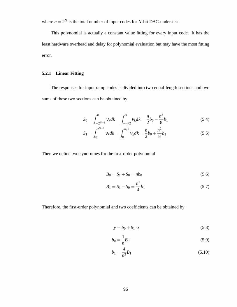
wheren= 2N is the total number of input codes forN-bit DAC-under-test.
This polynomial is actually a constant value fitting for every input code. It has the
least hardware overhead and delay for polynomial evaluation but may have the most fitting
error.
5.2.1 Linear Fitting
The responses for input ramp codes is divided into two equal-length sections and two
sums of these two sections can be obtained by
S0 =∫ 0
−2N−1νkdk=
∫ 0
−n/2νkdk=
n2
b0−n2
8b1 (5.4)
S1 =∫ 2N−1
0νkdk=
∫ n/2
0νkdk=
n2
b0+n2
8b1 (5.5)
Then we define two syndromes for the first-order polynomial
B0 = S1+S0 = nb0 (5.6)
B1 = S1−S0 =n2
4b1 (5.7)
Therefore, the first-order polynomial and two coefficients can be obtained by
y= b0+b1 ·x (5.8)
b0 =1n
B0 (5.9)
b1 =4n2B1 (5.10)
96
The two coefficients are proportional to offset and gain of the transfer function. Using
linear fitting, high order harmonic distortions are discarded and so fitting error is large for
DAC measurements. However, it is suitable for fitting ADC measurements because DSP
can only get ADC outputs in the unit of LSB so high order distortions are already lost.
5.2.2 Second-Order Fitting and Third-Order Fitting
The responses are divided into three equal-length sectionsfor second-order polyno-
mial. Each of three sections are accumulated up to obtain three sums
S0 =∫ −n/6
−n/2νkdk=
n3
b0−n2
9b1+
13n3
324b2 (5.11)
S1 =∫ n/6
−n/6νkdk=
n3
b0+n3
324b2 (5.12)
S2 =∫ n/2
n/6νkdk=
n3
b0+n2
9b1+
13n3
324b2 (5.13)
We then define three syndromes for the second-order polynomial
B0 = S2−26S1+S0 =−8nb0 (5.14)
B1 = S2−S0 =2n2
9b1 (5.15)
B2 = S2−2S1+S0 =2n3
27b2 (5.16)
97
Therefore, the second-order polynomial and three coefficients can be obtained by
y= b0+b1 ·x+b2 ·x2 (5.17)
b0 =− 18n
B0 (5.18)
b1 =9
2n2B1 (5.19)
b2 =272n3B2 (5.20)
The response is divided into four equal-length sections forthird-order polynomial, as dis-
cussed in [23, 24]. The sum of each section is
S0 =∫ −n/4
−n/2νkdk=
n4
b0−3n2
32b1+
7n3
192b2−
15n4
1024b3 (5.21)
S1 =∫ 0
−n/4νkdk=
n4
b0−n2
32b1+
n3
192b2−
n4
1024b3 (5.22)
S2 =∫ n/4
0νkdk=
n4
b0+n2
32b1+
n3
192b2+
n4
1024b3 (5.23)
S2 =∫ n/2
n/4νkdk=
n4
b0+3n2
32b1+
7n3
192b2+
15n4
1024b3 (5.24)
We can now define four syndromes as below (also same as in [23])
B0 = S3+S2+S1+S0 = nb0+n3
12b2 (5.25)
B1 = S3+S2−S1−S0 =n2
4b1+
n4
32b3 (5.26)
B2 = S3−S2−S1+S0 =n3
16b2 (5.27)
B3 = S3−3S2+3S1−S0 =3n4
128b3 (5.28)
98
Therefore, the third-order polynomial and four coefficients can be obtained by
y= b0+b1 ·x+b2 ·x2+b3 ·x3 (5.29)
b0 =1n(B0−
43
B2) (5.30)
b1 =4n2(B1−
43
B3) (5.31)
b2 =16n3 B2 (5.32)
b3 =1283n4 B3 (5.33)
These two polynomial fitting algorithms are used for DAC output fitting since the
nonlinearities caused by process variation in DAC are of second or third order type in most
case. So, employing a second or third order polynomial fitting algorithm may yield best
results.
5.2.3 Higher-Order Fitting
Repeat the procedure above and we can obtainN+1 syndromes by dividing output
responses intoN+1 equal-length sections. And thenN+1 coefficients forNth-order poly-
nomial can be calculated from these syndromes. In theory high-order polynomial may
result in better fitting results. However, higher-order polynomial may have much greater
penalty upon hardware overhead and delay, especially for high-order multiplies compu-
tation. We observed thatN=3 is sufficient in most cases so there is no need to explore
higher-order polynomial fitting equations.
99
5.3 Adaptive Fitting
We assume that the DSP and other digital circuitry have been tested and is fault-
free. Before actual testing of on-chip DAC under test, a loopback as shown in Figure 3.18
is established. The DSP sends a series of random numbers through its output port and
checks the input port for response. This step will detect anyinterconnect faults at DSP
input/output.
If the inconsistency among test code and ADC responses is smaller than the fault-
tolerance factor, the on-chip DAC-under-test (DUT) is considered fixable. Such inconsis-
tencies between test code (k) and m-DAC response (k) is actually the digitized and com-
bined integral nonlinearity (INL) errors of both DUT and m-DAC.
INLk =νk−ν0
LSB−k= k−k (5.34)
whereνk is N-bit DUT output and the least significant bit (LSB) is the minimal unit voltage
value for the DUT. For example, given reference voltageVre f , LSB of 14-bit DAC is
VLSB=Vre f
214 (5.35)
Because m-ADC is based on Sigma-Delta modulator and has high linearity with large OSR,
the INL error of m-ADC can be ignored and thusk−k can be considered as the INL error of
sole DUT for given codek. An adaptive polynomial fitting algorithm is employed to fit the
nonlinearity errors (INLk for each codek) of DUT to obtain the best-matching minimum
degree polynomial for nonlinearity characteristics of DUToutputs.
100
Consider an order-p fitting polynomial:
y= b0+b1 ·x+b2 ·x2+ · · ·+(p−1) ·xp−1+ p·xp (5.36)
whereb0, b1, b2, ...,bp−1, bp are polynomial coefficients. Best-matching polynomial gives
minimum mean-square error. To obtain the best-matching polynomial, we apply fitting to
data for successively increasing degrees of polynomials. Although a higher order polyno-
mial may have better fitting and lower error, it takes more time to calculate the coefficients,
will require more memory to store and will need more complex digital circuitry for calcula-
tion. Thus, a higher order polynomial will require more gates and delay than a lower order
one. Too high an order also brings meta-stability to system and negatively affects product
reliability. Therefore, make trade-off between fitting accuracy and fitting time/hardware
overhead. To make at-speed DAC correction possible, the maximum path delay of digital
polynomial calculation circuitry must not exceed DAC conversion delay. So for given pro-
cess and DAC design, maximum available order of polynomial shall be specified as well as
fault-tolerance factor.
Accuracy of matching polynomial can be determined as the root mean square (RMS)
error between measured INL errors and the polynomial values:
∆νk = νk− (ν0+k ·LSB) (5.37)
yrms=
√
√
√
√
12N
2N−1
∑k=0
(∆νk−y(k))2 (5.38)
101
for N-bit DAC-under-test. In the proposed BIST procedure, a low-order polynomial fitting
algorithm is used at first and then high-order ones, until theRMS errors drops below a
specified threshold. For each polynomial, two steps are executed: coefficients extraction
and polynomial evaluation. In coefficients extraction step, a series of consecutive ramp
codes are generated as test patterns to DUT, then the Sigma-Delta modulator will measure
DUT responses and DSP will collect both test patterns and DUTresponses to calculate cur-
rent polynomial coefficients for INL errors. In polynomial evaluation step, another series
of consecutive ramp codes will be generated to evaluate the polynomial with calculated
coefficients and obtain its RMS value for ramp codes. Thus the fitting accuracy of current
polynomial to INL errors of DUT outputs can be defined as the RMSvalue. In real im-
plementation, polynomial evaluation step of previous polynomial may be combined with
coefficients extraction of next polynomial because these two steps will be using different
hardware at the same time with possible race issue. The coefficients may also indicate if
DUT is correctable by comparing to pre-defined values.
We use Matlab to simulate the proposed adaptive self-calibration approach. INL errors
of a 14-bit DAC-under-test is shown in Figure 5.2 and we try various order polynomials to
fit the INL errors, as shown in Tables 5.1, 5.2, 5.3 and 5.4.
Figure 5.3 compares fitting curves of those three polynomials and RMS errors of each
order polynomials can also be calculated: 1.5188 for zero-order, 0.9643 for first-order,
0.8407 for second-order, and 0.0907 for third-order. It canbe observed that third-order
polynomial is the best match polynomial to fitting on-chip DAC in this case. It is possi-
ble that fourth-order polynomial may have better matching results but due to significant
102
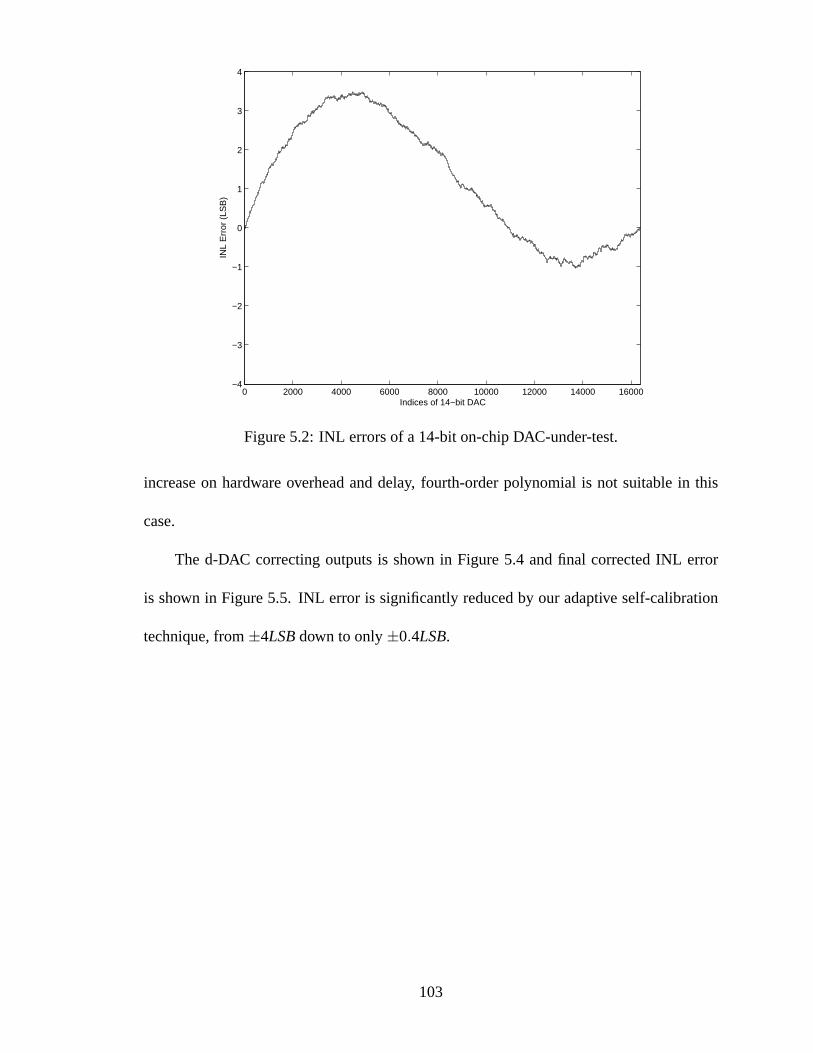
0 2000 4000 6000 8000 10000 12000 14000 16000−4
−3
−2
−1
0
1
2
3
4
Indices of 14−bit DAC
INL
Err
or (
LSB
)
Figure 5.2: INL errors of a 14-bit on-chip DAC-under-test.
increase on hardware overhead and delay, fourth-order polynomial is not suitable in this
case.
The d-DAC correcting outputs is shown in Figure 5.4 and final corrected INL error
is shown in Figure 5.5. INL error is significantly reduced by our adaptive self-calibration
technique, from±4LSBdown to only±0.4LSB.
103
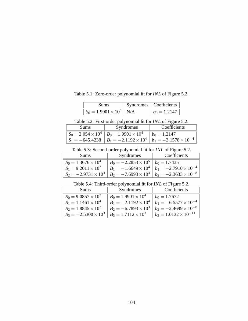
Table 5.1: Zero-order polynomial fit forINL of Figure 5.2.
Sums Syndromes Coefficients
S0 = 1.9901×10⁴ N/A b0 = 1.2147
Table 5.2: First-order polynomial fit forINL of Figure 5.2.Sums Syndromes Coefficients
S0 = 2.054×10⁴ B0 = 1.9901×10⁴ b0 = 1.2147S1 =−645.4238 B1 =−2.1192×10⁴ b1 =−3.1578×10⁻⁴
Table 5.3: Second-order polynomial fit forINL of Figure 5.2.Sums Syndromes Coefficients
S0 = 1.3676×10⁴ B0 =−2.2853×10⁵ b0 = 1.7435S1 = 9.2011×10³ B1 =−1.6649×10⁴ b1 =−2.7910×10⁻⁴
S2 =−2.9731×10³ B2 =−7.6993×10³ b2 =−2.3633×10⁻⁸
Table 5.4: Third-order polynomial fit forINL of Figure 5.2.Sums Syndromes Coefficients
S0 = 9.0857×10³ B0 = 1.9901×10⁴ b0 = 1.7672S1 = 1.1461×10⁴ B1 =−2.1192×10⁴ b1 =−6.5577×10⁻⁴
S2 = 1.8845×10³ B2 =−6.7893×10³ b2 =−2.4699×10⁻⁸
S3 =−2.5300×10³ B3 = 1.7112×10³ b3 = 1.0132×10⁻¹¹
104
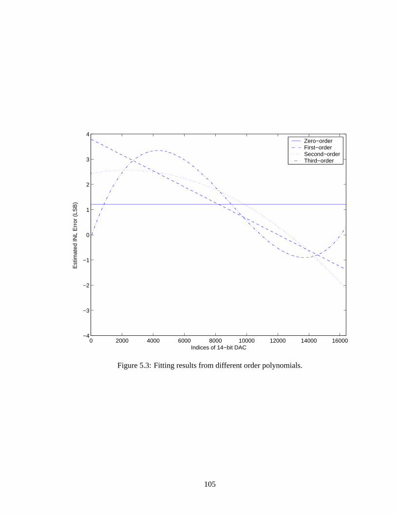
0 2000 4000 6000 8000 10000 12000 14000 16000−4
−3
−2
−1
0
1
2
3
4
Indices of 14−bit DAC
Est
imat
ed IN
L E
rror
(LS
B)
Zero−orderFirst−orderSecond−orderThird−order
Figure 5.3: Fitting results from different order polynomials.
105
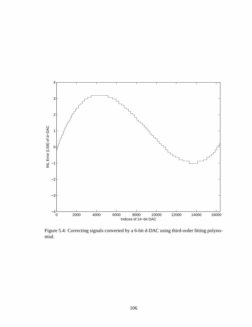
0 2000 4000 6000 8000 10000 12000 14000 16000−4
−3
−2
−1
0
1
2
3
4
Indices of 14−bit DAC
INL
Err
or (
LSB
) of
d−
DA
C
Figure 5.4: Correcting signals converted by a 6-bit d-DAC using third-order fitting polyno-mial.
106
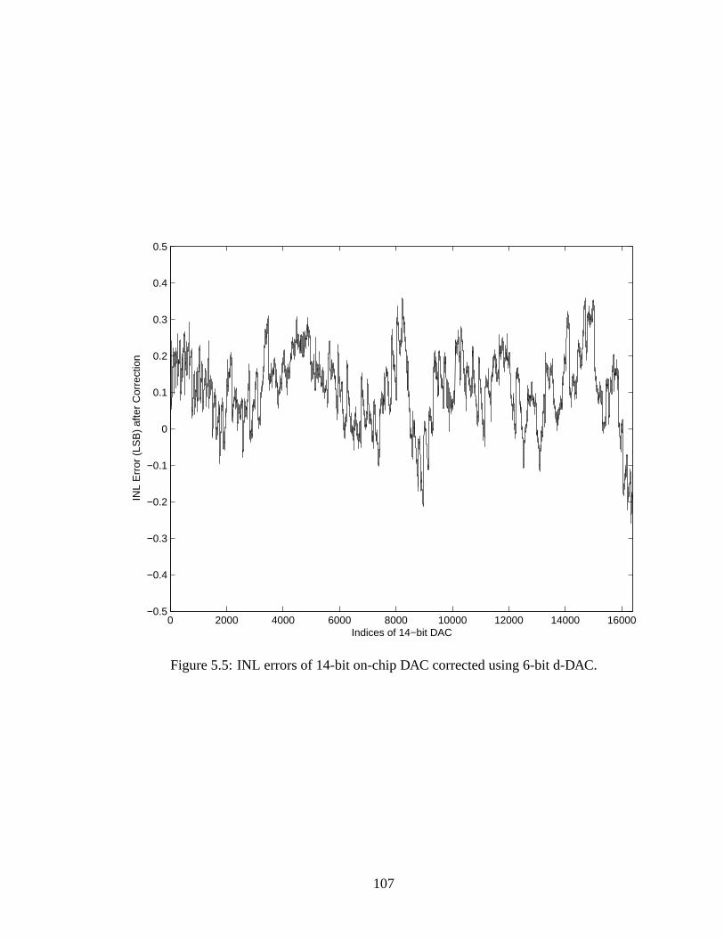
0 2000 4000 6000 8000 10000 12000 14000 16000−0.5
−0.4
−0.3
−0.2
−0.1
0
0.1
0.2
0.3
0.4
0.5
Indices of 14−bit DAC
INL
Err
or (
LSB
) af
ter
Cor
rect
ion
Figure 5.5: INL errors of 14-bit on-chip DAC corrected using6-bit d-DAC.
107

Chapter 6
Conclusion
The proposed BIST and calibration approach is verified, simulated and implemented
using tools such as Matlab, and Design Compiler. Matlab and SimuLink models are used to
build a systematic simulation environment to test the feasibility of the proposed approach.
Design Compiler is used to synthesize an implementation of polynomial evaluation unit
since this single unit occupies most area overhead due to multiply-accumulate operation
required by polynomial computation.
6.1 Truncation Error
Fix-point multiply-accumulate operation is used in the implementation because de-
sign of an IEEE-compatible float-point computation unit is too complicated and will take
much larger silicon area. However, using fixed-point calculation brings another problem in
addition to the existing nonlinearity errors that is truncation error. Given the fixed length
of data word, the precision is limited and the rest will be discarded. AssumingN-bit word
length, the range of the fixed-point number which a word may represent is,
−2N−1 ≤ n< 2N−1−1 (6.1)
For example, the range for a 10-bit word is -1024 to 1023.
108
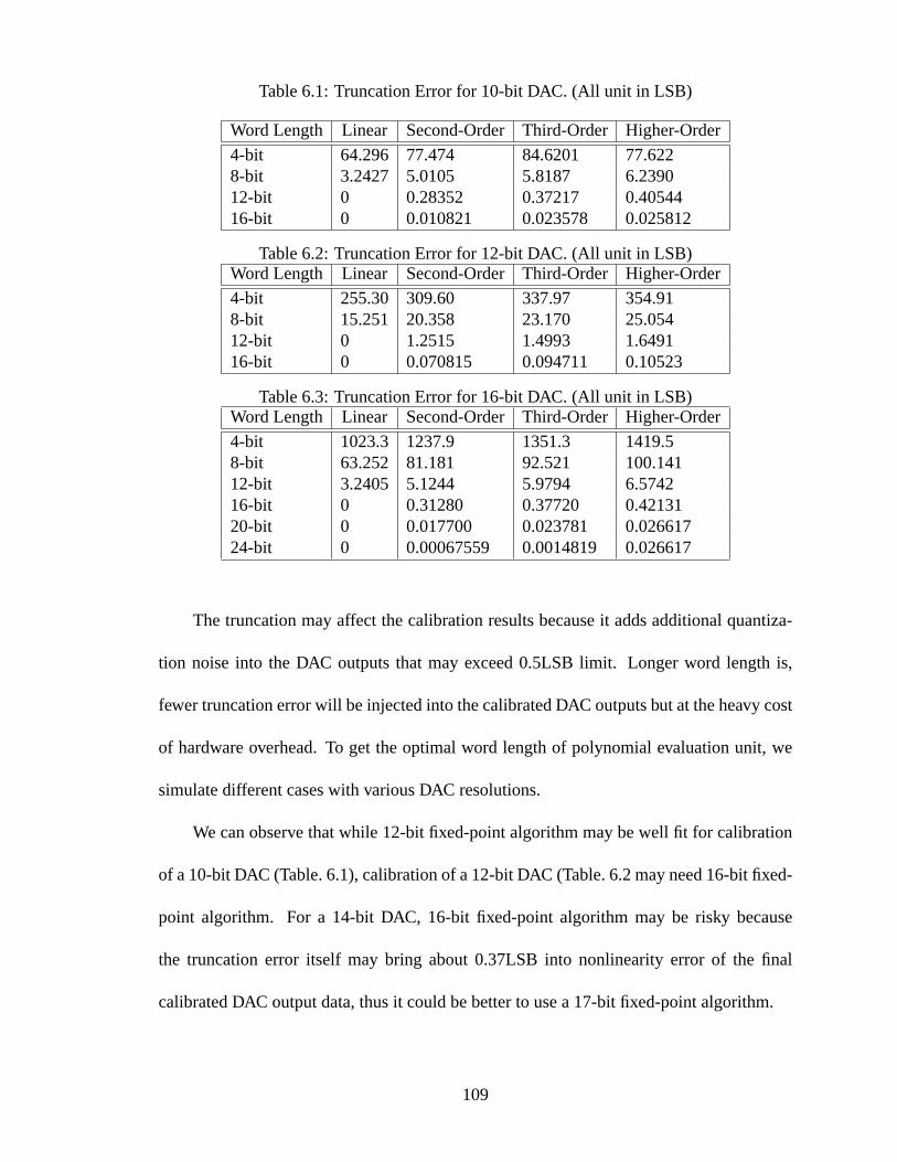
Table 6.1: Truncation Error for 10-bit DAC. (All unit in LSB)
Word Length Linear Second-Order Third-Order Higher-Order
4-bit 64.296 77.474 84.6201 77.6228-bit 3.2427 5.0105 5.8187 6.239012-bit 0 0.28352 0.37217 0.4054416-bit 0 0.010821 0.023578 0.025812
Table 6.2: Truncation Error for 12-bit DAC. (All unit in LSB)Word Length Linear Second-Order Third-Order Higher-Order
4-bit 255.30 309.60 337.97 354.918-bit 15.251 20.358 23.170 25.05412-bit 0 1.2515 1.4993 1.649116-bit 0 0.070815 0.094711 0.10523
Table 6.3: Truncation Error for 16-bit DAC. (All unit in LSB)Word Length Linear Second-Order Third-Order Higher-Order
4-bit 1023.3 1237.9 1351.3 1419.58-bit 63.252 81.181 92.521 100.14112-bit 3.2405 5.1244 5.9794 6.574216-bit 0 0.31280 0.37720 0.4213120-bit 0 0.017700 0.023781 0.02661724-bit 0 0.00067559 0.0014819 0.026617
The truncation may affect the calibration results because it adds additional quantiza-
tion noise into the DAC outputs that may exceed 0.5LSB limit.Longer word length is,
fewer truncation error will be injected into the calibratedDAC outputs but at the heavy cost
of hardware overhead. To get the optimal word length of polynomial evaluation unit, we
simulate different cases with various DAC resolutions.
We can observe that while 12-bit fixed-point algorithm may bewell fit for calibration
of a 10-bit DAC (Table. 6.1), calibration of a 12-bit DAC (Table. 6.2 may need 16-bit fixed-
point algorithm. For a 14-bit DAC, 16-bit fixed-point algorithm may be risky because
the truncation error itself may bring about 0.37LSB into nonlinearity error of the final
calibrated DAC output data, thus it could be better to use a 17-bit fixed-point algorithm.
109
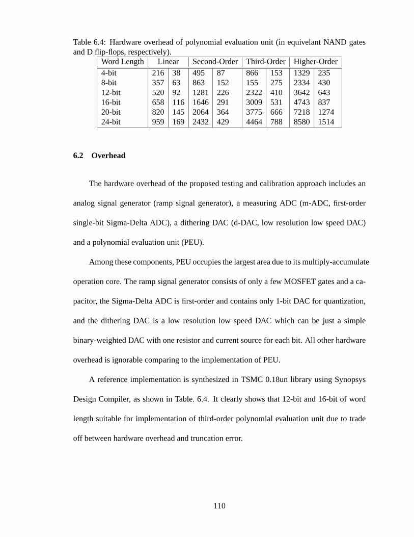
Table 6.4: Hardware overhead of polynomial evaluation unit(in equivelant NAND gatesand D flip-flops, respectively).
Word Length Linear Second-Order Third-Order Higher-Order
4-bit 216 38 495 87 866 153 1329 2358-bit 357 63 863 152 155 275 2334 43012-bit 520 92 1281 226 2322 410 3642 64316-bit 658 116 1646 291 3009 531 4743 83720-bit 820 145 2064 364 3775 666 7218 127424-bit 959 169 2432 429 4464 788 8580 1514
6.2 Overhead
The hardware overhead of the proposed testing and calibration approach includes an
analog signal generator (ramp signal generator), a measuring ADC (m-ADC, first-order
single-bit Sigma-Delta ADC), a dithering DAC (d-DAC, low resolution low speed DAC)
and a polynomial evaluation unit (PEU).
Among these components, PEU occupies the largest area due toits multiply-accumulate
operation core. The ramp signal generator consists of only afew MOSFET gates and a ca-
pacitor, the Sigma-Delta ADC is first-order and contains only 1-bit DAC for quantization,
and the dithering DAC is a low resolution low speed DAC which can be just a simple
binary-weighted DAC with one resistor and current source for each bit. All other hardware
overhead is ignorable comparing to the implementation of PEU.
A reference implementation is synthesized in TSMC 0.18un library using Synopsys
Design Compiler, as shown in Table. 6.4. It clearly shows that12-bit and 16-bit of word
length suitable for implementation of third-order polynomial evaluation unit due to trade
off between hardware overhead and truncation error.
110
6.3 Test Time
Although testing time of the proposed approach is not as critical as other factors like
nonlinearity error, truncation error and hardware overhead, it is still worth estimation. The
testing steps employed by the proposed approach only happens during chip power-up and
they run only to characterize on-chip ADC and DAC, extract coefficients of fitting polyno-
mials, verify the calibrated DAC and ADC. Thus the normal operation of ADC/DAC and
other analog/digital circuitry in SoC system will not be affected by the testing time after
test accomplishes.
Assuming on-chip ADC/DAC under-test is ofN-bit resolution and their sampling and
conversion time isT, oversampling ratio of m-ADC (first-order single-bit Sigma-Delta
ADC) is M and d-DAC resolution isN′, we get
Td1 = 2N ·M ·T (6.2)
Td2 = 2N ·M ·T (6.3)
Tad = 2N ·T (6.4)
Tda = 2N ·M ·T (6.5)
Tv = 2N′ ·M ·T (6.6)
whereTd1 is the diagnosis time for analog signal generator and m-ADC,Td2 is the diagnosis
time for d-DAC and m-ADC,Tad is the testing time of on-chip ADC,Tda is the testing time
of on-chip DAC, andTv is the testing time for verification of calibrated ADC/DAC.
111
Thus the total testing time is:
Ttotal = 2N+1 ·T · (M+1)+2N ·T ·M (6.7)
To consider a typical case, let on-chip ADC/DAC resolution be14 bits with a 10ns
conversion time, OSR of m-ADC be 2000 and assume a 6-bit resolution for the d-DAC
used for calibrating the DAC. Then, the total test time is 657ms.
6.4 Summary
A DSP-based adaptive self-calibration BIST scheme is proposed to test and diagnose
on-chip DAC with best-matching polynomial fitting algorithm. A Sigma-Delta modulator-
based measuring ADC is used to measure on-chip DAC outputs. The native nonlinear-
ity errors of Sigma-Delta modulator are ignored by selecting sufficient oversampling ratio
(OSR). The order and coefficients of best-matching polynomial can be calculated to retrieve
nonlinearity errors as output correcting code. A low-resolution dither DAC is employed to
convert digital correcting code to analog correcting signals for DAC output. This BIST
scheme will be executed every time when SoC starts up to get up-to-date characteristics of
on-chip DAC. The adaptive self-calibration approach has been verified by simulation and
shows significant improvement of linearity for noisy on-chip DAC output.
112
Bibliography
[1] “World Semiconductor Trade Statistics (WSTS),” 2005. http://www.wsts.org/.
[2] D. Boning and J. Chung, “Statistical Metrology: Understanding Spatial Variation inSemicondictor Manufacturing,” inProc. SPIE - The International Society for OpticalEngineering, Dec. 1996, pp. 16–26.
[3] L. Rolindez, S. Mir, G. Prenat, and A. Bounceur, “A 0.18µ CMOS Implementationof On-chip Analogue Test Signal Generation from Digital Test Patterns,” inProc.Design, Automation and Test in Europe Conference, 2004, pp. 704–705.
[4] F. F. Dai and C. E. Stroud, “Analog and Mixed-Signal Test Architectures,” in L.-T. Wang, C. E. Stroud, and N. A. Touba, editors,System-on-Chip Test Architecures:Nanometer Design for Testability, chapter 15, pp. 703–743, Morgan Kaufmann, 2008.
[5] J. Wang, E. Sanchez-Sinencio, and F. Maloberti, “Very Linear Ramp-Generators forHigh Resolution ADC BIST and Calibration,” inProc. 43rd IEEE Midwest Symp. onCircuits and Systems, Aug. 2000, pp. 908–911.
[6] “IEEE Standard Test Access Port and Boundary - Scan Architecture IEEE Std 1149.1-1990.”
[7] “IEEE Standard for Reduced-Pin and Enhanced-Functionality Test Access Port andBoundary-Scan Architecture IEEE Std 1149.7-2009.”
[8] N. Nicolici, B. M. Al-Hashimi, A. D. Brown, and A. Williams,“BIST HardwareSynthesis for RTL Data Paths Based on Test Compatibility Classes,” IEEE Trans.Computer-Aided Design of Integrated Circuits and Systems, vol. 19, no. 11, pp. 1375–1385, Nov. 2001.
[9] A. McWilliams, editor,Analog and Mixed Signal Devices: Market Research Report.BCC, March 2007.
[10] “International Technology Roadmap for Semiconductors,” 2007. http://www.itrs.net/Links/2007ITRS/Home2007.htm.
[11] “International Technology Roadmap for Semiconductors,” 2005. http://www.itrs.net/Links/2005ITRS/Home2005.htm.
[12] “IEEE Standard for a Mixed-Signal Test Bus IEEE Std 1149.4-1999.”
[13] R.-W. Liu, editor,Testing and Diagnosis of Analog Circuits and Systems. Van Nos-trand Reinhold, 1991.
113
[14] B. Vinnakota, editor,Analog and Mixed-Signal Test. Prentice-Hall PTR, 1998.
[15] R. Rashidzadeh, M. Ahmadi, and W. C. Miller, “Test and Measurement of Analog andRF Cores in Mixed-Signal SoC Environment,”IEEE Trans. Computer-Aided Designof Integrated Circuits and Systems, vol. 26, no. 10, pp. 1855–1865, Oct. 2007.
[16] T. Kuyel, “Linearity Testing Issues of Analog to Digital Converters,” inProc. Inter-national Test Conference, 1999, pp. 747–756.
[17] W. Dai and J. Hao, “Timing analysis taking into account interconnect process vari-ation,” in Proc. IEEE International Workshop on Statistical Methodology, 2001, pp.51–53.
[18] D. K. Schroder, “Negative Bias Temperature Instability: What Do We Understand?,”Microeletronics Reliability, vol. 47, pp. 841–852, June 2007.
[19] M. L. Bushnell and V. D. Agrawal,Essentials of Testing for Digital, Memory &Mixed-Signal VLSI Circuits. Boston: Springer, 2000.
[20] M. Ehsanian, B. Kaminska, and K. Arabi, “A New Digital Test Approach for Analog-to-Digital Converter Testing,” inProc. IEEE International Workshop on StatisticalMethodology, 2001, pp. 51–53.
[21] S. Max, “Fast Accurate and Complete ADC Testing,” inProc. International TestConf., 1989, pp. 111–117.
[22] B. Dufort and G. W. Roberts, “On-Chip Analog Signal Generation for Mixed-SignalBuilt-In Self-Test,”IEEE Journal of Solid-State Circuits, vol. 34, no. 3, pp. 318–330,Mar. 1999.
[23] S. Sunter and N. Nagi, “A Simplified Polynomial Fitting Algorithm for DAC andADC BIST,” in Proc. International Test Conference, 1997, pp. 389–395.
[24] A. Roy, S. Sunter, A. Fudoli, and D. Appelo, “High Accuracy Stimulus Generation forA/D Converter BIST,” inProc. International Test Conference, 2002, pp. 1031–1039.
[25] W. Jiang and V. D. Agrawal, “Built-in Self-Calibration ofOn-Chip DAC and ADC,”in Proc. International Test Conference, Oct. 2008. Paper No. 32.2.
[26] W. Jiang and V. D. Agrawal, “Designing Variation-Tolerance in Mixed-Signal Com-ponents of a System-on-Chip,” inProc. IEEE International Symposium on Circuitsand Systems, 2009, pp. 126–129.
[27] W. Jiang and V. D. Agrawal, “A DSP-Based Ramp Test for On-Chip High-ResolutionADC,” in Proc. 43rd IEEE Southeastern Symp. System Theory, Mar. 2011, pp. 205–209.
[28] H. Yu, J. A. Abraham, S. Hwang, and J. Roh, “Efficient Loop-back Testing of On-Chip ADCs and DACs,” inProc. Asia and South Pacific Design Automation Conf.,volume 21-24, Jan. 2003, pp. 651–656.
114
[29] L. Jin, H. Haggag, R. Geiger, and D. Chen, “Testing of Precision DACs Using Low-Resolution ADCs with Dithering,” inProc. International Test Conf., 2006. Paper13.1.
[30] M. G. Flores, M. Negreiros, L. Carro, A. A. Susin, F. R. Clayton, and C. Benevento,“Low Cost BIST for Static and Dynamic Testing of ADCs,”Journal of ElectronicTesting: Theory and Applications, vol. 21, pp. 283–290, 2005.
[31] K. Arabi and B. Kaminska, “Efficient and Accurate Testingof Analog-to-Digital Con-verters Using Oscillation-Test Method,” inProc. European Conference on Design andTest, 1997, pp. 348–352.
[32] J.-L. Huang and K.-T. Cheng, “A Sigma-Delta Modulation Based BIST Scheme forMixed-Signal Circuits,” inProc. Asia and South Pacific Design Automation Conf.,Jan. 2000, pp. 605–610.
[33] K.-J. Lee, S.-J. Chang, and R.-S. Tzeng, “A Sigma-Delta Modulation Based BISTScheme for A/D Converters,” inProc. 12th Asian Test Symp., 2003, pp. 124–127.
[34] C.-K. Ong, K.-T. Cheng, and L.-C. Wang, “Delta-Sigma Modulator Based Mixed-Signal BIST Architecture for SoC,” inProc. Asia and South Pacific Design Automa-tion Conf., Jan. 2003, pp. 669–674.
[35] G. Yu, P. Li, and W. Dong, “Achieving Low-Cost Linearity Test and Diagnosis ofΣ∆ADCs via Frequency-Domain Nonlinear Analysis and Macromodeling,” in Proc. 8thInternational Symposium on Quality Electronic Design, Mar. 2007, pp. 513–518.
[36] D. D. Venuto and L. Reyneri, “Fully Digital Optimized Testing and Calibration Tech-nique forΣ∆ ADC’s,” in Proc. 8th International Symposium on Quality ElectronicDesign, Mar. 2007, pp. 519–526.
[37] G. Yu and P. Li, “Lookup Table Based Simulation and Statistical Modeling of Sigma-Delta ADCs,” inProc. Design Automation Conference, July 2006, pp. 1035–1040.
[38] J. Chen and Y. Xu, “A Novel Noise-Shaping DAC for Multi-BitSigma-Delta Modu-lator,” IEEE Trans. on Circuits and Systems, vol. 53, pp. 334–348, May 2006.
[39] D. D. Venuto, “New Test Access for High-ResolutionΣ∆ ADC’s by Using the NoiseTransfer Function Evaluation,” inProc, International Symposium on Quality Elec-tronic Design, 2004, pp. 81–85.
[40] C. K. Ong, K. T. Cheng, and L. C. Wang, “A New Sigma-Delta Modulator Archi-tecture for Testing Using Digital Stimulus,”IEEE Trans. on Circuits and Systems-I,vol. 51, pp. 206–213, Jan. 2004.
[41] R. Radke, A. Eshraghi, and T. S. Fiez, “A Spurious-Free Delta-Sigma DAC UsingRotated Data Weighted Averaging,” inProc. IEEE Custom Integrated Circuits Con-ference, May 1999, pp. 125–128.
115
[42] A. Yasuda, H. Tanimoto, and T. Iida, “A Third-Order∆−Σ Modulator Using Second-Order Noise-Shaping Dynamic Element Matching,”IEEE Journal of Solid-State Cir-cuits, vol. 33, pp. 1879–1886, Dec. 1998.
[43] I. H. S. Hassan, K. Arabi, and B. Kaminska, “Testing Digital to Analog ConvertersBased on Oscillation Test Strategy Using Sigma-Delta Modulation,” in Proc. Inter-national Conference on Computer Design: VLSI in Computers and Processors, Oct.1998, pp. 40–46.
[44] T. Shui, R. Schreier, and F. Hudson, “An Oversampled A/D Converter Using Cas-caded Fourth Order Sigma-Delta Modulation and Current Steering Logic,” in Proc.IEEE International Symposium on Circuits and Systems, volume 1, June 1998, pp.412–415.
[45] T. Shui, R. Schreier, and F. Hudson, “Mismatch-Shaping DAC for Lowpass and Band-pass Multi-Bit Delta-Sigma Modulators,” inProc. IEEE International Symposium onCircuits and Systems, volume 1, May 1998, pp. 352–355.
[46] P. Benabes, M. Keramat, and R. Kielbasa, “A Methodology for DesigningContinuous-Time Sigma-Delta Modulators,” inProceeding of European Design andTest Conference, Mar. 1997, pp. 46–50.
[47] F. Chen and B. H. Leung, “A High Resolution Multibit Sigma-Delta Modulator withIndividual Level Averaging,”IEEE Journal of Solid-State Circuits, vol. 30, pp. 453–460, Apr. 1995.
[48] X. Xu and M. S. P. Lucas, “Variable-Sampling-Rate Sigma-Delta Modulator for In-strumentation and Measurement,”IEEE Trans. on Instrumentation and Measurement,vol. 44, pp. 929–932, Oct. 1995.
[49] Y.-S. Wang, J.-X. Wang, F.-C. Lai, and Y.-Z. Ye, “A Low-Cost BIST Scheme forADC Testing,” inProc. 6th International Conf. on ASIC, volume 2, Oct. 2005, pp.694–698.
[50] H. Xing, D. chen, and R. L. Geiger, “Linearity Test for High Resolution DACs UsingLow-Accuracy DDEM Flash ADCs,” inProc. IEEE International Symp. Circuits andSystems, May 2006, pp. 2469–2472.
[51] S. Max, “Ramp Testing of ADC Transition Levels using Finite Resolution Ramps,”in Proc. International Test Conference, 2001, pp. 495–501. Paper No. 18.1.
[52] Y. J. Chang, S. J. Chang, J. C. Ho, C. K. Ong, T. Cheng, and W. C. Wu,“Built-InHigh Resolution Signal Generator for Testing ADC and DAC,” inProc. InternationalSymposium on VLSI Technology, Systems, and Applications, 2003, pp. 231–234.
[53] J. Rogers, C. Plett, and F. Dai,Integrated Circuit Design for High-Speed FrequencySynthesis. Boston: Artech House, 2006.
[54] M. F. Toner and G. W. Roberts, “A BIST Techniques for a Frequency Response andIntermodulation Distortion Test of a Sigma-Delta ADC,” inProc. IEEE VLSI TestSymposium, Apr. 1994, pp. 60–65.
116
[55] M. F. Toner and G. W. Roberts, “A BIST Scheme for a SNR, Gain Tracking, andFrequency Response Test of a Sigma-Delta ADC,”IEEE Trans. Circuits and SystemsII: Analog and Digital Signal Processing, vol. 42, no. 1, pp. 1–15, Jan. 1995.
[56] J. Doernberg, H.-S. Lee, and D. A. Hodges, “Full-speed testing of A/D converters,”IEEE Journal of Solid-State Circuits, vol. 19, pp. 820–827, Dec. 1984.
[57] H. Jiang, D. Chen, and R. L. Geiger, “Dither Incorporated Deterministic DynamicElement Matching for High Resolution ADC Test Using Extremely Low Resolu-tion DACs,” in Proc. IEEE International Symp. Circuits and Systems, May 2005,pp. 4285–4288.
[58] J. L. LaMay and H. T. Bogard, “How to Obtain Maximum Practical Performancefrom State of the Art Delta-Sigma Analog to Digital Converters,” IEEE Trans. onInstrumentation and Measurement, vol. 41, pp. 861–867, Dec. 1992.
[59] P. Arpaia, F. Cennamo, P. Daponte, and H. Schumny, “Modeling and Characterizationof Sigma-Delta Analog-to-Digital Converters,” inProc. IEEE Instrumentation andMeasurement Technology Conference, May 1998, pp. 96–100.
[60] J. C. Candy and G. C. Temes,Oversampling Methods for A/D D/A Conversion, Over-sampling Delta-Sigma Converters. New Jersey: IEEE Press, 1992. pp. 2-3.
[61] I. Mehr and T. L. Sculley, “Oversampling Current Sample/Hold Structure for DigitalCMOS Process Implementation,”IEEE Trans. Circuits and Systems II: Analog andDigital Signal Processing, vol. 45, no. 2, pp. 196–203, Feb. 1998.
[62] S. Haykin,An Introduction to Analog and Digital Communication. New York: JohnWiley & Sons, 1989. See pages 187-197 and 323-326.
117

Appendices
118

Appendix A
Abbreviations
ADC Analog-to-Digital ConverterATE Automatic Test EquipmentBIST Built-In Self-TestCUT Circuit Under Testd-DAC Dithering DACDAC Digital-to-Analog ConverterDFF D Flip-FlopDFT Design For TestDNL Differential Non-LinearityDR Dynamic RangeDSP Digital Signal ProcessorDUT Design Under TestENOB Effective Number of BitsFFT Fast Fourier TransformIC Integrated CircuitIEEE Institute of Electrical and Electronics EngineersIM3 Third-Order IntermodulationINL Integral Non-LinearityIP3 Third-order Intercept PointITRS International Technology Roadmap for SemiconductorsJTAG Joint Test Action GroupLPF Low-Pass FilterLSB Lease Significant Bitm-ADC Measuring ADCMATLAB A high-level technical computing language from MathWorksMOS Metal-Oxide SemiconductorMOSFET MOS Field Effect TransistorNBTI Negative Bias Temperature InstabilityORA Output Response AnalyzerOSR Oversampling RatioPEU Polynomial Evaluation UnitPWM Pulse-Width ModulationRMS Root Mean Square
119

SDFF Scan D Flip-FlopSimulink A MATLAB simulation and design system from MathWorksSINAD Signal-to-Noise-and-Distortion RatioSNR Signal-to-Noise RatioSNDR Signal-to-Noise-and-Distortion RatioSoC System-on-ChipTHD Total Harmonic DistortionTPG Test Pattern Generator
120

Appendix B
OSR and SNR of Sigma-Delta Modulation
Assuming a sufficiently high over sampling rate (OSR) such that f 2s ≫ f 2
0 , the rms
noise magnitude in the signal band of a first-order Sigma-Delta modulator is,
n0 = ermsπ√3(OSR)−3/2 (B.1)
The rms noise magnitude in the signal band of a second-order Sigma-Delta modulator is,
n0 = ermsπ2√
5(OSR)−5/2 (B.2)
The rms noise magnitude in the signal band of a higher-order Sigma-Delta modulator is,
n0 = ermsπn
√2n+1
(OSR)−(2n+1)/2 (B.3)
The SNR with oversampling and noise shaping can be found. Therms noise magni-
tude in the signal band of second-order Sigma-Delta modulator is,
SNR = 10log
[
18
(
2N −1)2∆2
∆2
12π2n
2n+1OSR−(2n+1)
]
(B.4)
= 10log
[
32·22N ·SNR2n+1 ·
(
π2n
2n+1
)−1]
(B.5)
121
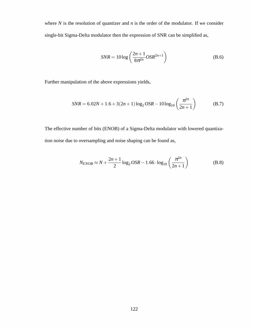
whereN is the resolution of quantizer andn is the order of the modulator. If we consider
single-bit Sigma-Delta modulator then the expression of SNR can be simplified as,
SNR= 10log
(
2n+18π2n OSR2n+1
)
(B.6)
Further manipulation of the above expressions yields,
SNR= 6.02N+1.6+3(2n+1) log2OSR−10log10
(
π2n
2n+1
)
(B.7)
The effective number of bits (ENOB) of a Sigma-Delta modulator with lowered quantiza-
tion noise due to oversampling and noise shaping can be foundas,
NENOB≈ N+2n+1
2log2OSR−1.66· log10
(
π2n
2n+1
)
(B.8)
122