bridgetek pte ltd ft800 - welcome to bridgetekbridgetek pte ltd ft800 (embedded video engine) the...
TRANSCRIPT
Copyright © Bridgetek Pte Ltd 1
FT800 Embedded Video Engine Datasheet Version 1.3
Document No.: BRT_000039 Clearance No.: BRT#001
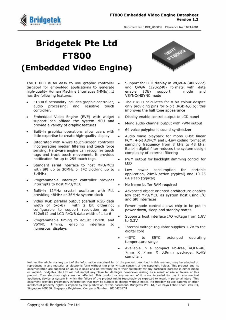
Bridgetek Pte Ltd
FT800
(Embedded Video Engine)
The FT800 is an easy to use graphic controller targeted for embedded applications to generate high-quality Human Machine Interfaces (HMIs). It has the following features:
FT800 functionality includes graphic controller,
audio processing, and resistive touch
controller.
Embedded Video Engine (EVE) with widget support can offload the system MPU and provide a variety of graphic features
Built-in graphics operations allow users with little expertise to create high-quality display
Integrated with 4-wire touch-screen controller
incorporating median filtering and touch force sensing. Hardware engine can recognize touch tags and track touch movement. It provides notification for up to 255 touch tags.
Standard serial interface to host MPU/MCU with SPI up to 30MHz or I²C clocking up to
3.4MHz
Programmable interrupt controller provides interrupts to host MPU/MCU
Built-in 12MHz crystal oscillator with PLL providing 48MHz or 36MHz system clock
Video RGB parallel output (default RGB data width of 6-6-6) with 2 bit dithering;
configurable to support resolution up to 512x512 and LCD R/G/B data width of 1 to 6
Programmable timing to adjust HSYNC and VSYNC timing, enabling interface to numerous displays
Support for LCD display in WQVGA (480x272) and QVGA (320x240) formats with data enable (DE) support mode and VSYNC/HSYNC mode
The FT800 calculates for 8-bit colour despite
only providing pins for 6-bit (RGB-6,6,6); this
improves the half tone appearance
Display enable control output to LCD panel
Mono audio channel output with PWM output
64 voice polyphonic sound synthesizer
Audio wave playback for mono 8-bit linear PCM, 4-bit ADPCM and µ-Law coding format at sampling frequency from 8 kHz to 48 kHz.
Built-in digital filter reduces the system design complexity of external filtering
PWM output for backlight dimming control for LED
Low power consumption for portable application, 24mA active (typical) and 10-25
uA sleep (typical)
No frame buffer RAM required
Advanced object oriented architecture enables low cost MPU/MCU as system host using I2C and SPI interfaces
Power mode control allows chip to be put in power down, sleep and standby states
Supports host interface I/O voltage from 1.8V to 3.3V
Internal voltage regulator supplies 1.2V to the digital core
-40°C to 85°C extended operating temperature range
Available in a compact Pb-free, VQFN-48,
7mm X 7mm X 0.9mm package, RoHS compliant
Neither the whole nor any part of the information contained in, or the product described in this manual, may be adapted or
reproduced in any material or electronic form without the prior written consent of the copyright holder. This product and its
documentation are supplied on an as-is basis and no warranty as to their suitability for any particular purpose is either made
or implied. Bridgetek Pte Ltd will not accept any claim for damages howsoever arising as a result of use or failure of this product. Your statutory rights are not affected. This product or any variant of it is not intended for use in any medical
appliance, device or system in which the failure of the product might reasonably be expected to result in personal injury. This
document provides preliminary information that may be subject to change without notice. No freedom to use patents or other
intellectual property rights is implied by the publication of this document. Bridgetek Pte Ltd, 178 Paya Lebar Road, #07-03,
Singapore 409030. Singapore Registered Company Number: 201542387H
Copyright © Bridgetek Pte Ltd 2
FT800 Embedded Video Engine Datasheet Version 1.3
Document No.: BRT_000039 Clearance No.: BRT#001
1 Typical Applications
Point of Sales Machines
Multi-function Printers
Instrumentation
Home Security Systems
Graphic touch pad – remote, dial pad
Tele / Video Conference Systems
Phones and Switchboards
Medical Appliances
Blood Pressure displays
Heart monitors
Glucose level displays
Breathalyzers
Gas chromatographs
Power meter
Home appliance devices
Set-top box
Thermostats
Sprinkler system displays
Medical Appliances
GPS / SatNav
Vending Machine Control Panels
Elevator Controls
……and many more
1.1 Part Numbers
Part Number Package
FT800Q-x 48 Pin VQFN, pitch 0.5mm, body 7mm x 7mm x 0.9mm
Table 1- Video Controller Part Numbers
Note: Packaging codes for x is:
-R: Taped and Reel, (VQFN in 2500 pieces per reel)
-T: Tray packing, (VQFN in 250 pieces per tray)
For example: FT800Q-R is 2500 VQFN pieces in taped and reel packaging
Copyright © Bridgetek Pte Ltd 3
FT800 Embedded Video Engine Datasheet Version 1.3
Document No.: BRT_000039 Clearance No.: BRT#001
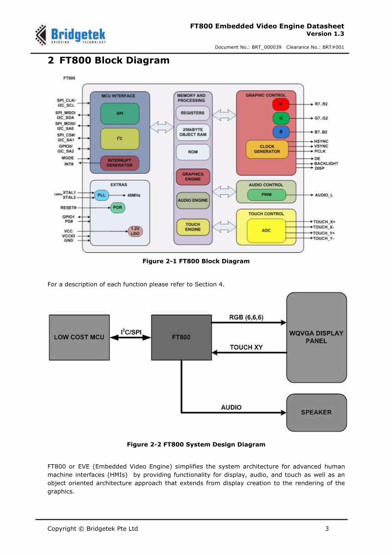
2 FT800 Block Diagram
Figure 2-1 FT800 Block Diagram
For a description of each function please refer to Section 4.
Figure 2-2 FT800 System Design Diagram
FT800 or EVE (Embedded Video Engine) simplifies the system architecture for advanced human
machine interfaces (HMIs) by providing functionality for display, audio, and touch as well as an
object oriented architecture approach that extends from display creation to the rendering of the
graphics.
Copyright © Bridgetek Pte Ltd 4
FT800 Embedded Video Engine Datasheet Version 1.3
Document No.: BRT_000039 Clearance No.: BRT#001
Table of Contents
1 Typical Applications ................................................. 2
1.1 Part Numbers ...................................................................... 2
2 FT800 Block Diagram .............................................. 3
3 Device Pin Out and Signal Description ..................... 6
3.1 VQFN-48 Package Pin Out ................................................... 6
3.2 Pin Description .................................................................... 7
4 Function Description ............................................. 11
4.1 Serial Host Interface ......................................................... 11
4.1.1 SPI Interface .................................................................................... 13
4.1.2 I²C Interface .................................................................................... 13
4.1.3 Serial Data Protocol........................................................................... 13
4.1.4 Host Memory Read ............................................................................ 13
4.1.5 Host Memory Write ........................................................................... 14
4.1.6 Host Command ................................................................................. 14
4.1.7 Interrupts ........................................................................................ 15
4.2 System Clock ..................................................................... 16
4.2.1 Clock Source .................................................................................... 16
4.2.2 Phase Locked Loop ............................................................................ 17
4.2.3 Clock Enable .................................................................................... 17
4.2.4 Clock Frequency ............................................................................... 18
4.3 Graphics Engine ................................................................ 18
4.3.1 Introduction ..................................................................................... 18
4.3.2 ROM and RAM Fonts .......................................................................... 18
4.4 Parallel RGB Interface ....................................................... 22
4.5 Miscellaneous Control ....................................................... 23
4.5.1 Backlight Control Pin ......................................................................... 23
4.5.2 DISP Control Pin ............................................................................... 23
4.5.3 General Purpose IO pins .................................................................... 23
4.5.4 Pins Drive Current Control .................................................................. 23
4.6 Audio Engine ..................................................................... 24
4.6.1 Sound Synthesizer ............................................................................ 24
4.6.2 Audio Playback ................................................................................. 26
4.7 Touch-Screen Engine ......................................................... 26
Copyright © Bridgetek Pte Ltd 5
FT800 Embedded Video Engine Datasheet Version 1.3
Document No.: BRT_000039 Clearance No.: BRT#001
4.8 Power Management ........................................................... 28
4.8.1 Power supply .................................................................................... 28
4.8.2 Internal Regulator and POR ................................................................ 28
4.8.3 Power Modes .................................................................................... 29
5 FT800 Memory Map ............................................... 33
5.1 FT800 Registers ................................................................ 34
6 Devices Characteristics and Ratings ...................... 38
6.1 Absolute Maximum Ratings ............................................... 38
6.2 DC Characteristics ............................................................. 38
6.3 Touch Sense Characteristics .............................................. 40
6.4 AC Characteristics ............................................................. 41
6.4.1 System clock .................................................................................... 41
6.4.2 Host Interface SPI Mode 0 ................................................................. 41
6.4.3 Host Interface I2C Mode Timing .......................................................... 42
6.4.4 RGB Video Timing ............................................................................. 43
7 Application Examples ............................................ 45
7.1 Examples of LCD Interface connection .............................. 45
7.2 Examples of PWM Audio Circuits ....................................... 45
8 Package Parameters .............................................. 46
8.1 VQFN-48 Package Dimensions ........................................... 46
8.1.1 Top Side ............................................................................................... 46
8.1.2 Bottom Side .......................................................................................... 46
8.2 VQFN-48 Package Dimensions ........................................... 47
8.3 Solder Reflow Profile ......................................................... 48
9 Contact Information .............................................. 49
Appendix A – References ............................................. 50
Document References ................................................................ 50
Acronyms and Abbreviations ..................................................... 50
Appendix B - List of Figures and Tables ....................... 51
List of Figures ............................................................................ 51
List of Tables ............................................................................. 51
Appendix C - Revision History ...................................... 53
Copyright © Bridgetek Pte Ltd 6
FT800 Embedded Video Engine Datasheet Version 1.3
Document No.: BRT_000039 Clearance No.: BRT#001
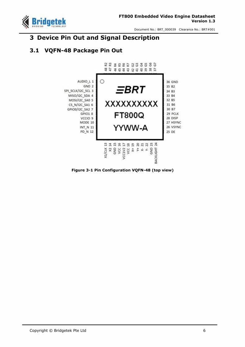
3 Device Pin Out and Signal Description
3.1 VQFN-48 Package Pin Out
Figure 3-1 Pin Configuration VQFN-48 (top view)
Copyright © Bridgetek Pte Ltd 7
FT800 Embedded Video Engine Datasheet Version 1.3
Document No.: BRT_000039 Clearance No.: BRT#001
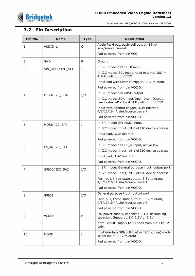
3.2 Pin Description
Pin No. Name Type Description
1 AUDIO_L O Audio PWM out, push-pull output, 16mA sink/source current.
Pad powered from pin VCC.
2 GND P Ground
3 SPI_SCLK/ I2C_SCL I In SPI mode: SPI SCLK input.
In I2C mode: SCL input, need external 1kΩ ~ 4.7kΩ pull up to VCCIO.
Input pad with Schmitt trigger, 3.3V tolerant.
Pad powered from pin VCCIO.
4 MISO/ I2C_SDA I/O In SPI mode: SPI MISO output.
In I2C mode: SDA input/Open Drain Output, need external1kΩ ~ 4.7kΩ pull up to VCCIO.
Input with Schmitt trigger, 3.3V tolerant,
4/8/12/16mA sink/source current.
Pad powered from pin VCCIO.
5 MOSI/ I2C_SA0 I In SPI mode: SPI MOSI input.
In I2C mode: Input, bit 0 of I2C device address.
Input pad, 3.3V tolerant.
Pad powered from pin VCCIO.
6 CS_N/ I2C_SA1 I In SPI mode: SPI CS_N input, active low.
In I2C mode: Input, bit 1 of I2C device address.
Input pad, 3.3V tolerant.
Pad powered from pin VCCIO.
7 GPIO0/ I2C_SA2 I/O In SPI mode: General purpose input, output port.
In I2C mode: Input, bit 2 of I2C device address.
Push-pull, three-state output. 3.3V tolerant, 4/8/12/16mA sink/source current.
Pad powered from pin VCCIO.
8 GPIO1 I/O General purpose input, output port.
Push-pull, three-state output. 3.3V tolerant, 4/8/12/16mA sink/source current.
Pad powered from pin VCCIO.
9 VCCIO P I/O power supply, connect a 0.1uF decoupling
capacitor. Support 1.8V, 2.5V or 3.3V.
Note: VCCIO supply to IO pads from pin 3 to 12
only.
10 MODE I Host interface SPI(pull low) or I2C(pull up) mode select input, 3.3V tolerant
Pad powered from pin VCCIO.
Copyright © Bridgetek Pte Ltd 8
FT800 Embedded Video Engine Datasheet Version 1.3
Document No.: BRT_000039 Clearance No.: BRT#001
Pin No. Name Type Description
11 INT_N OD Host Interrupt, open drain output, active low, pull up to VCCIO through a 1kΩ ~10kΩ resistor.
12 PD_N I Power down input, active low, 3.3V tolerant, pull up to VCCIO through 47kΩ resistor and 100nF to ground.
Pad powered from pin VCCIO.
13 X1/ CLK I Crystal oscillator or clock input; Connect to GND if not used.
3.3V peak input allowed.
Pad powered from pin VCC.
14 X2 O Crystal oscillator output; leave open if not used.
Pad powered from pin VCC.
15 GND P Ground
16 VCC P 3.3V power supply input.
17 VCC1V2 O 1.2V regulator output pin. Connect a 4.7uF decoupling capacitor to GND.
18 VCC P 3.3V power supply input.
19 X+ AI/O Connect to X right electrode of 4-wire touch-
screen panel.
Pad powered from pin VCC.
20 Y+ AI/O Connect to Y top electrode of 4-wire touch-screen panel.
Pad powered from pin VCC.
21 X- AI/O Connect to X left electrode of 4-wire touch-screen panel.
Pad powered from pin VCC.
22 Y- AI/O Connect to Y bottom electrode of 4-wire touch-screen panel.
Pad powered from pin VCC.
23 GND P Ground
24 BACKLIGHT O LED Backlight brightness PWM controls signal, push-pull output, 4/8mA sink/source current.
Pad powered from pin VCC.
25 DE O LCD Data Enable, push-pull output, 4/8mA
sink/source current.
Pad powered from pin VCC.
26 VSYNC O LCD Vertical Sync, push-pull output, 4/8mA
sink/source current.
Pad powered from pin VCC.
27 HSYNC O LCD Horizontal Sync, push-pull output, 4/8mA sink/source current.
Copyright © Bridgetek Pte Ltd 9
FT800 Embedded Video Engine Datasheet Version 1.3
Document No.: BRT_000039 Clearance No.: BRT#001
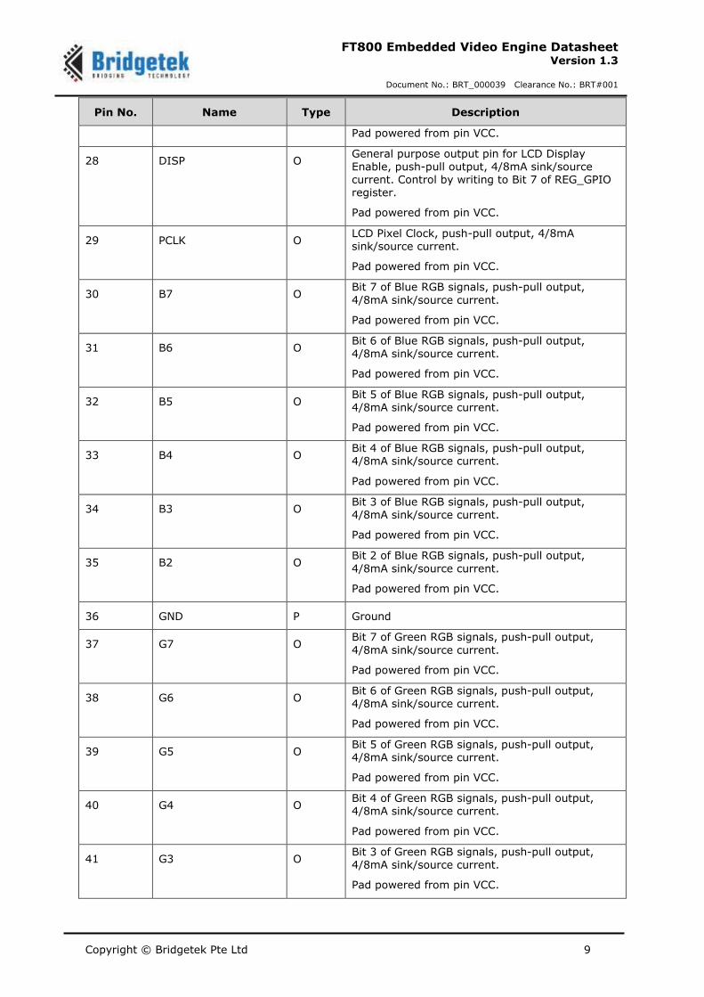
Pin No. Name Type Description
Pad powered from pin VCC.
28 DISP O General purpose output pin for LCD Display Enable, push-pull output, 4/8mA sink/source current. Control by writing to Bit 7 of REG_GPIO register.
Pad powered from pin VCC.
29 PCLK O LCD Pixel Clock, push-pull output, 4/8mA sink/source current.
Pad powered from pin VCC.
30 B7 O Bit 7 of Blue RGB signals, push-pull output,
4/8mA sink/source current.
Pad powered from pin VCC.
31 B6 O Bit 6 of Blue RGB signals, push-pull output, 4/8mA sink/source current.
Pad powered from pin VCC.
32 B5 O Bit 5 of Blue RGB signals, push-pull output, 4/8mA sink/source current.
Pad powered from pin VCC.
33 B4 O Bit 4 of Blue RGB signals, push-pull output, 4/8mA sink/source current.
Pad powered from pin VCC.
34 B3 O Bit 3 of Blue RGB signals, push-pull output, 4/8mA sink/source current.
Pad powered from pin VCC.
35 B2 O Bit 2 of Blue RGB signals, push-pull output,
4/8mA sink/source current.
Pad powered from pin VCC.
36 GND P Ground
37 G7 O Bit 7 of Green RGB signals, push-pull output,
4/8mA sink/source current.
Pad powered from pin VCC.
38 G6 O Bit 6 of Green RGB signals, push-pull output, 4/8mA sink/source current.
Pad powered from pin VCC.
39 G5 O Bit 5 of Green RGB signals, push-pull output, 4/8mA sink/source current.
Pad powered from pin VCC.
40 G4 O Bit 4 of Green RGB signals, push-pull output, 4/8mA sink/source current.
Pad powered from pin VCC.
41 G3 O Bit 3 of Green RGB signals, push-pull output, 4/8mA sink/source current.
Pad powered from pin VCC.
Copyright © Bridgetek Pte Ltd 10
FT800 Embedded Video Engine Datasheet Version 1.3
Document No.: BRT_000039 Clearance No.: BRT#001
Pin No. Name Type Description
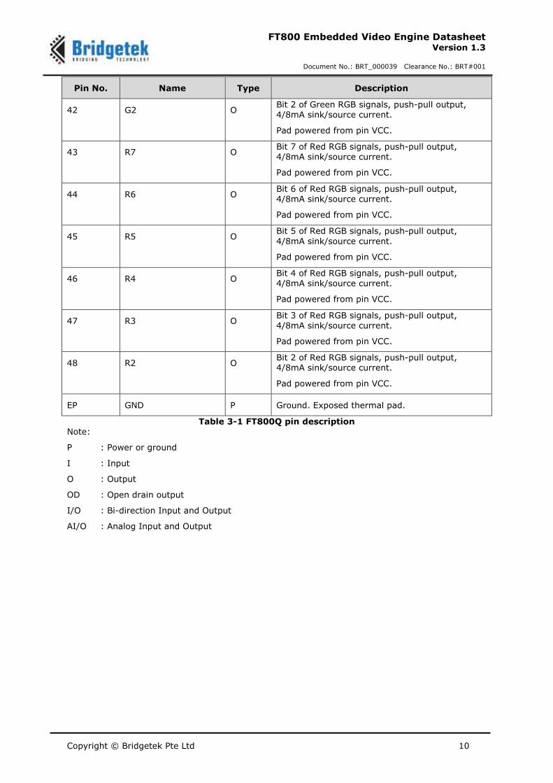
42 G2 O Bit 2 of Green RGB signals, push-pull output, 4/8mA sink/source current.
Pad powered from pin VCC.
43 R7 O Bit 7 of Red RGB signals, push-pull output, 4/8mA sink/source current.
Pad powered from pin VCC.
44 R6 O Bit 6 of Red RGB signals, push-pull output, 4/8mA sink/source current.
Pad powered from pin VCC.
45 R5 O Bit 5 of Red RGB signals, push-pull output,
4/8mA sink/source current.
Pad powered from pin VCC.
46 R4 O Bit 4 of Red RGB signals, push-pull output, 4/8mA sink/source current.
Pad powered from pin VCC.
47 R3 O Bit 3 of Red RGB signals, push-pull output, 4/8mA sink/source current.
Pad powered from pin VCC.
48 R2 O Bit 2 of Red RGB signals, push-pull output, 4/8mA sink/source current.
Pad powered from pin VCC.
EP GND P Ground. Exposed thermal pad.
Table 3-1 FT800Q pin description Note:
P : Power or ground
I : Input
O : Output
OD : Open drain output
I/O : Bi-direction Input and Output
AI/O : Analog Input and Output
Copyright © Bridgetek Pte Ltd 11
FT800 Embedded Video Engine Datasheet Version 1.3
Document No.: BRT_000039 Clearance No.: BRT#001
4 Function Description
The FT800 is a single chip, embedded graphic controller with the following function blocks: Serial Host Interface System Clock Graphics Engine Parallel RGB video interface Audio Engine
Touch-screen Engine Power Management
The functions for each block are briefly described in the following subsections.
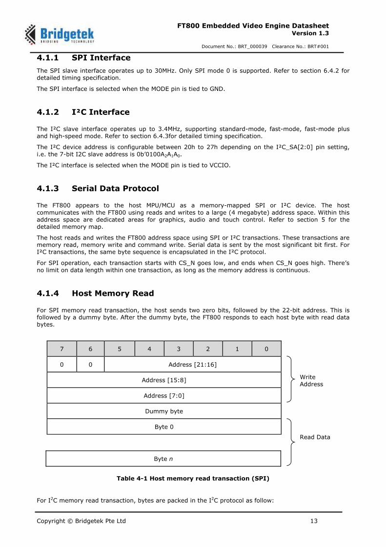
4.1 Serial Host Interface
The FT800 uses a standard serial interface to communicate with most types of microcontrollers and microprocessors. The interface mode is configurable by pull down for SPI and pull up for I²C on pin 10
(MODE). Figure 4-1 shows the two alternative mode connections.
Figure 4-1 Host Interface Options

Copyright © Bridgetek Pte Ltd 12
FT800 Embedded Video Engine Datasheet Version 1.3
Document No.: BRT_000039 Clearance No.: BRT#001
Figure 4-2 illustrates a direct connection to a 1.8-3.3V IO MPU/MCU.
Figure 4-2 SPI Interface 1.8-3.3V connection
Figure 4-3 illustrates the FT800 connected to a 5V IO MPU/MCU. The 74LCX125 logic buffer can tolerate 5V signal from the MPU/MCU, and the FT800 input signals are limited to 3.3V.
Figure 4-3 SPI Interface 5V connection
GND GND
CS_N
MISO
MOSI
SCLK
PD_N
INT_N
CS_N
MISO
MOSI
SCLK
PD_N
INT_N
FT800
1.8-3.3V
Vio
3.3V
VCC4.7k 4.7kMPU/MCU
3.3V GND
5V
GND GND
CS_N
MISO
MOSI
SCLK
PD_N
INT_N
CS_N
MISO
MOSI
SCLK
PD_N
INT_N
FT800MPU/MCU
74LCx125
3.3V
Vio VCC
4.7K 4.7K
Copyright © Bridgetek Pte Ltd 13
FT800 Embedded Video Engine Datasheet Version 1.3
Document No.: BRT_000039 Clearance No.: BRT#001
4.1.1 SPI Interface
The SPI slave interface operates up to 30MHz. Only SPI mode 0 is supported. Refer to section 6.4.2 for detailed timing specification.
The SPI interface is selected when the MODE pin is tied to GND.
4.1.2 I²C Interface
The I²C slave interface operates up to 3.4MHz, supporting standard-mode, fast-mode, fast-mode plus and high-speed mode. Refer to section 6.4.3for detailed timing specification.
The I²C device address is configurable between 20h to 27h depending on the I²C_SA[2:0] pin setting,
i.e. the 7-bit I2C slave address is 0b’0100A2A1A0.
The I²C interface is selected when the MODE pin is tied to VCCIO.
4.1.3 Serial Data Protocol
The FT800 appears to the host MPU/MCU as a memory-mapped SPI or I²C device. The host
communicates with the FT800 using reads and writes to a large (4 megabyte) address space. Within this address space are dedicated areas for graphics, audio and touch control. Refer to section 5 for the detailed memory map.
The host reads and writes the FT800 address space using SPI or I²C transactions. These transactions are memory read, memory write and command write. Serial data is sent by the most significant bit first. For I²C transactions, the same byte sequence is encapsulated in the I²C protocol.
For SPI operation, each transaction starts with CS_N goes low, and ends when CS_N goes high. There’s
no limit on data length within one transaction, as long as the memory address is continuous.
4.1.4 Host Memory Read
For SPI memory read transaction, the host sends two zero bits, followed by the 22-bit address. This is followed by a dummy byte. After the dummy byte, the FT800 responds to each host byte with read data bytes.
Byte n
Table 4-1 Host memory read transaction (SPI)
For I2C memory read transaction, bytes are packed in the I2C protocol as follow:
7 6 5 4 3 2 1 0
0 0 Address [21:16]
Address [15:8]
Address [7:0]
Dummy byte
Byte 0
Read Data
Write Address
Copyright © Bridgetek Pte Ltd 14
FT800 Embedded Video Engine Datasheet Version 1.3
Document No.: BRT_000039 Clearance No.: BRT#001
[start] <DEVICE ADDRESS + write bit>
<00b+Address[21:16]> <Address[15:8]> <Address[7:0]>
[restart] <DEVICE ADDRESS + read bit> <Read data byte 0> .... <Read data byte n>[stop]
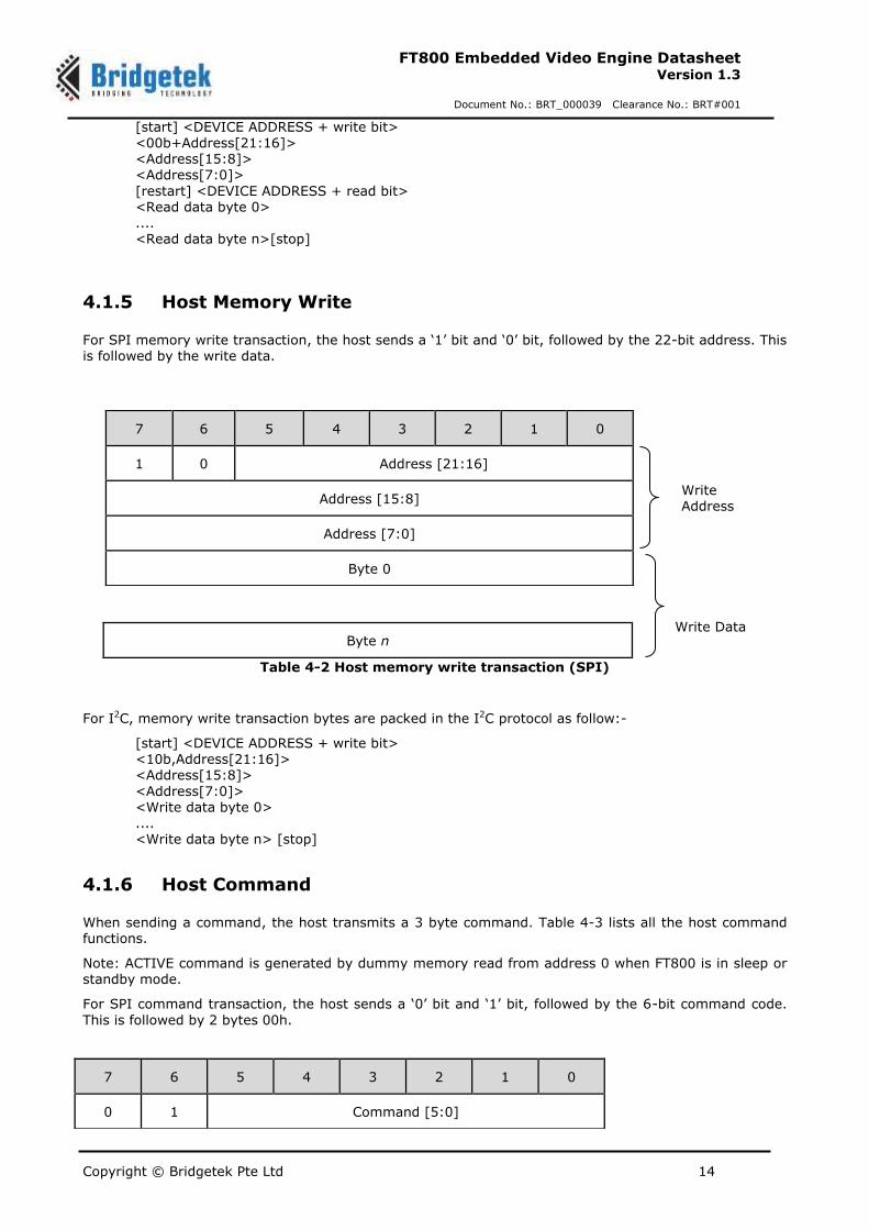
4.1.5 Host Memory Write
For SPI memory write transaction, the host sends a ‘1’ bit and ‘0’ bit, followed by the 22-bit address. This is followed by the write data.
Byte n
Table 4-2 Host memory write transaction (SPI)
For I2C, memory write transaction bytes are packed in the I2C protocol as follow:-
[start] <DEVICE ADDRESS + write bit> <10b,Address[21:16]> <Address[15:8]>
<Address[7:0]> <Write data byte 0> .... <Write data byte n> [stop]
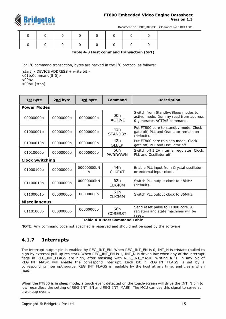
4.1.6 Host Command
When sending a command, the host transmits a 3 byte command. Table 4-3 lists all the host command functions.
Note: ACTIVE command is generated by dummy memory read from address 0 when FT800 is in sleep or standby mode.
For SPI command transaction, the host sends a ‘0’ bit and ‘1’ bit, followed by the 6-bit command code.
This is followed by 2 bytes 00h.
7 6 5 4 3 2 1 0
1 0 Address [21:16]
Address [15:8]
Address [7:0]
Byte 0
7 6 5 4 3 2 1 0
0 1 Command [5:0]
Write Data
Write Address
Copyright © Bridgetek Pte Ltd 15
FT800 Embedded Video Engine Datasheet Version 1.3
Document No.: BRT_000039 Clearance No.: BRT#001
Table 4-3 Host command transaction (SPI)
For I2C command transaction, bytes are packed in the I2C protocol as follows:
[start] <DEVICE ADDRESS + write bit> <01b,Command[5:0]> <00h> <00h> [stop]
1st Byte 2nd byte 3rd byte Command Description
Power Modes
00000000b 00000000b 00000000b 00h
ACTIVE
Switch from Standby/Sleep modes to active mode. Dummy read from address 0 generates ACTIVE command.
01000001b 00000000b 00000000b 41h
STANDBY
Put FT800 core to standby mode. Clock gate off, PLL and Oscillator remain on (default).
01000010b 00000000b 00000000b 42h
SLEEP Put FT800 core to sleep mode. Clock gate off, PLL and Oscillator off.
01010000b 00000000b 00000000b 50h
PWRDOWN Switch off 1.2V internal regulator. Clock, PLL and Oscillator off.
Clock Switching
01000100b 00000000b 00000000bN
A
44h
CLKEXT Enable PLL input from Crystal oscillator or external input clock.
01100010b 00000000b 00000000bN
A
62h
CLK48M Switch PLL output clock to 48MHz (default).
01100001b 00000000b 00000000b 61h
CLK36M Switch PLL output clock to 36MHz.
Miscellaneous
01101000b 00000000b 00000000b 68h
CORERST
Send reset pulse to FT800 core. All registers and state machines will be reset.
Table 4-4 Host Command Table
NOTE: Any command code not specified is reserved and should not be used by the software
4.1.7 Interrupts
The interrupt output pin is enabled by REG_INT_EN. When REG_INT_EN is 0, INT_N is tristate (pulled to high by external pull-up resistor). When REG_INT_EN is 1, INT_N is driven low when any of the interrupt flags in REG_INT_FLAGS are high, after masking with REG_INT_MASK. Writing a ‘1’ in any bit of REG_INT_MASK will enable the correspond interrupt. Each bit in REG_INT_FLAGS is set by a corresponding interrupt source. REG_INT_FLAGS is readable by the host at any time, and clears when read.
When the FT800 is in sleep mode, a touch event detected on the touch-screen will drive the INT_N pin to low regardless the setting of REG_INT_EN and REG_INT_MASK. The MCU can use this signal to serve as a wakeup event.
0 0 0 0 0 0 0 0
0 0 0 0 0 0 0 0
Copyright © Bridgetek Pte Ltd 16
FT800 Embedded Video Engine Datasheet Version 1.3
Document No.: BRT_000039 Clearance No.: BRT#001
Bit 7 6 5 4
Interrupt Sources CONVCOMPLETE CMDFLAG CMDEMPTY PLAYBACK
Conditions Touch-screen conversions completed
Command FIFO flag
Command FIFO empty
Audio playback ended
Bit 3 2 1 0
Interrupt Sources SOUND TAG TOUCH SWAP
Conditions Sound effect ended
Touch-screen tag value change
Touch-screen touch detected
Display list swap occurred
Table 4-5 Interrupt Flags bit assignment
4.2 System Clock
4.2.1 Clock Source
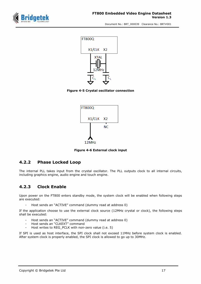
The FT800 can be configured to use any of the three clock sources for system clock:
Internal relaxation oscillator clock
External 12MHz crystal
External 12MHz square wave clock
Figure 4-5 and Figure 4-6 shows the pin connections for these clock options. Commands CLKEXT and
CLKINT switch between internal oscillator and external crystal oscillator and are synchronised to VSYNC on the fly.
The external crystal oscillator is recommended for applications which require higher quality audio reproduction.
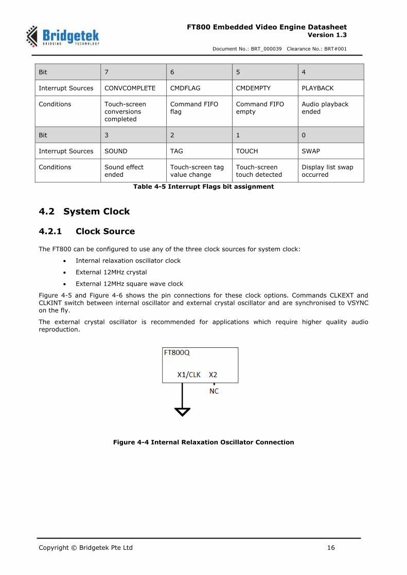
Figure 4-4 Internal Relaxation Oscillator Connection
Copyright © Bridgetek Pte Ltd 17
FT800 Embedded Video Engine Datasheet Version 1.3
Document No.: BRT_000039 Clearance No.: BRT#001
Figure 4-5 Crystal oscillator connection
Figure 4-6 External clock input
4.2.2 Phase Locked Loop
The internal PLL takes input from the crystal oscillator. The PLL outputs clock to all internal circuits, including graphics engine, audio engine and touch engine.
4.2.3 Clock Enable
Upon power on the FT800 enters standby mode, the system clock will be enabled when following steps are executed:
- Host sends an “ACTIVE” command (dummy read at address 0)
If the application choose to use the external clock source (12MHz crystal or clock), the following steps shall be executed:
- Host sends an “ACTIVE” command (dummy read at address 0)
- Host sends an “CLKEXT” command
- Host writes to REG_PCLK with non-zero value (i.e. 5)
If SPI is used as host interface, the SPI clock shall not exceed 11MHz before system clock is enabled. After system clock is properly enabled, the SPI clock is allowed to go up to 30MHz.
Copyright © Bridgetek Pte Ltd 18
FT800 Embedded Video Engine Datasheet Version 1.3
Document No.: BRT_000039 Clearance No.: BRT#001
4.2.4 Clock Frequency
Upon power-on the internal relaxation oscillator is untrimmed. The frequency range could be quite wide from chip to chip (refer to table x-y for internal relaxation oscillator specifications). If the application
utilises the internal clock without external clock source, it is recommended to perform clock trimming by software for better performance. For the details of clock trimming mechanism please refer to application note AN_299_FT800_FT801_Internal_Clock_Trimming [FTDI Document FT000987].
By default the system clock is 48MHz when the input clock is 12MHz. Host is allowed to switch the system clock between 48MHz and 36MHz by the host command “CLK48MHz” and “CLK36MHz” respectively. The clock switching is synchronised to VSYNC edge on the fly. This is to avoid possible graphics glitch during
clock switching. As a result, the clock switch will only take effect if the REG_PCLK is a non-zero value.
4.3 Graphics Engine
4.3.1 Introduction
The graphics engine executes the display list once for every horizontal line. It executes the primitive objects in the display list and constructs the display line buffer. The horizontal pixel content in the line buffer is updated if the object is visible at the horizontal line.
Main features of the graphics engine are:
The primitive objects supported by the graphics processor are: lines, points, rectangles, bitmaps (comprehensive set of formats), text display, plotting bar graph, edge strips, and line strips, etc.
Operations such as stencil test, alpha blending and masking are useful for creating a rich set of effects such as shadows, transitions, reveals, fades and wipes.
Anti-aliasing of the primitive objects (except bitmaps) gives a smoothing effect to the viewer. Bitmap transformations enable operations such as translate, scale and rotate. Display pixels are plotted with 1/16th pixel precision. Four levels of graphics states
Tag buffer detection
The graphics engine also supports customized build-in widgets and functionalities such as jpeg decode, screen saver, calibration etc. The graphics engine interprets commands from the MPU host via a 4 Kbyte FIFO in FT800 memory at RAM_CMD. The MPU/MCU writes commands into the FIFO, and the graphics engine reads and executes the commands. The MPU/MCU updates register REG_CMD_WRITE to indicate that there are new commands in the FIFO, and the graphics engine updates REG_CMD_READ after commands have been executed.
Main features supported are:
Drawing of widgets such as buttons, clock, keys, gauges, text displays, progress bars, sliders, toggle switches, dials, gradients, etc.
JPEG decode (Only baseline is supported) Inflate functionality (zlib inflate is supported) Timed interrupt (generate an interrupt to host processor after a specified number of
milliseconds)
In built animated functionalities such as displaying logo, calibration, spinner, screen saver and sketch
Snapshot feature to capture the current graphics display
For a complete list of graphics engine display commands and widgets refer to FT800 Series Programmers Guide, Chapter 4.
4.3.2 ROM and RAM Fonts
The FT800 has built in ROM character bitmaps as font metrics. The graphics engine can use these metrics when drawing text fonts. There are total 16 ROM fonts, numbered with font handle 16-31. The user can
Copyright © Bridgetek Pte Ltd 19
FT800 Embedded Video Engine Datasheet Version 1.3
Document No.: BRT_000039 Clearance No.: BRT#001
define and load customized font metrics into RAM_G, which can be used by display command with handle
0-15.
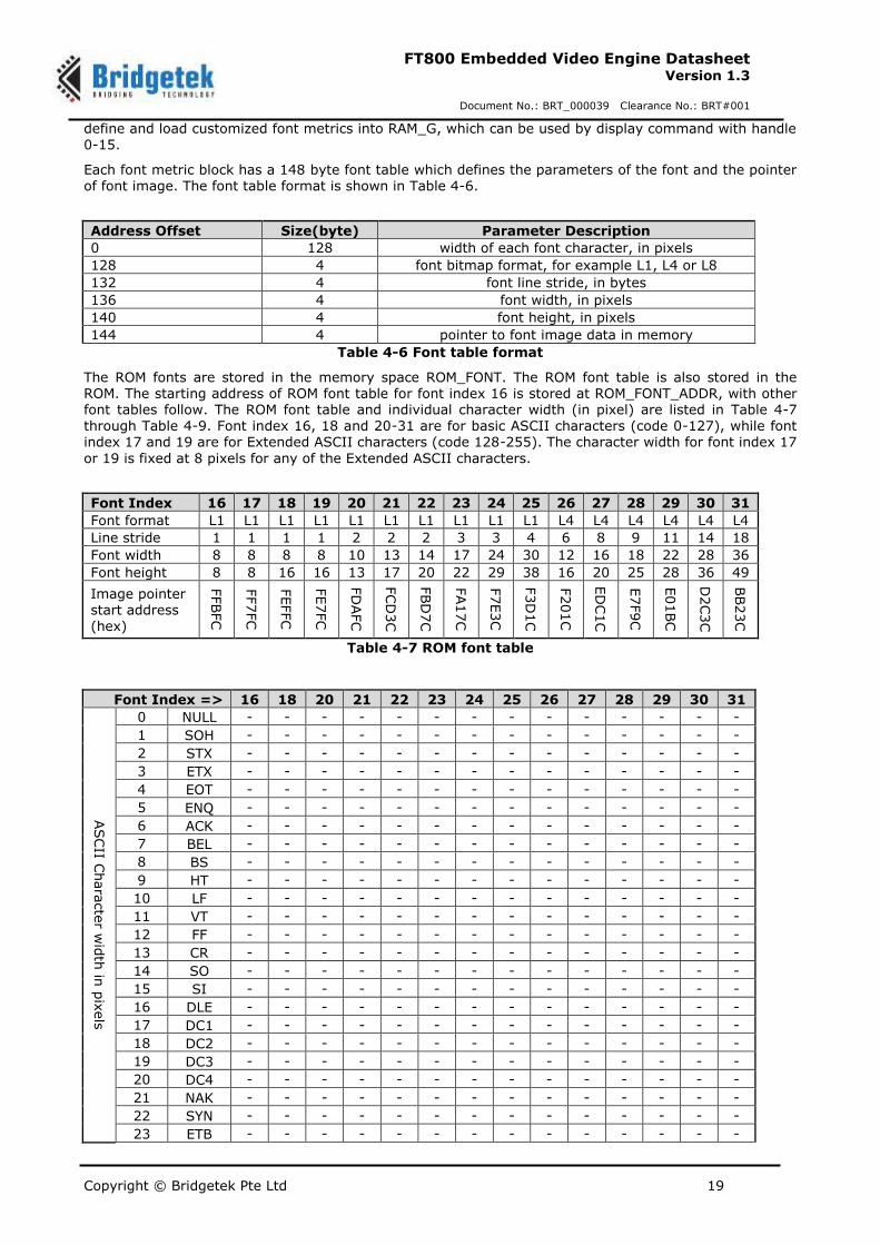
Each font metric block has a 148 byte font table which defines the parameters of the font and the pointer of font image. The font table format is shown in Table 4-6.
Address Offset Size(byte) Parameter Description
0 128 width of each font character, in pixels
128 4 font bitmap format, for example L1, L4 or L8
132 4 font line stride, in bytes
136 4 font width, in pixels
140 4 font height, in pixels
144 4 pointer to font image data in memory
Table 4-6 Font table format
The ROM fonts are stored in the memory space ROM_FONT. The ROM font table is also stored in the ROM. The starting address of ROM font table for font index 16 is stored at ROM_FONT_ADDR, with other font tables follow. The ROM font table and individual character width (in pixel) are listed in Table 4-7
through Table 4-9. Font index 16, 18 and 20-31 are for basic ASCII characters (code 0-127), while font index 17 and 19 are for Extended ASCII characters (code 128-255). The character width for font index 17
or 19 is fixed at 8 pixels for any of the Extended ASCII characters.
Font Index 16 17 18 19 20 21 22 23 24 25 26 27 28 29 30 31
Font format L1 L1 L1 L1 L1 L1 L1 L1 L1 L1 L4 L4 L4 L4 L4 L4
Line stride 1 1 1 1 2 2 2 3 3 4 6 8 9 11 14 18
Font width 8 8 8 8 10 13 14 17 24 30 12 16 18 22 28 36
Font height 8 8 16 16 13 17 20 22 29 38 16 20 25 28 36 49
Image pointer start address (hex)
FFBFC
FF7FC
FEFFC
FE7FC
FD
AFC
FCD
3C
FBD
7C
FA17C
F7E3C
F3D
1C
F201C
ED
C1C
E7F9C
E01BC
D2C3C
BB23C
Table 4-7 ROM font table
Font Index => 16 18 20 21 22 23 24 25 26 27 28 29 30 31
ASCII C
hara
cte
r wid
th in
pix
els
0 NULL - - - - - - - - - - - - - -
1 SOH - - - - - - - - - - - - - -
2 STX - - - - - - - - - - - - - -
3 ETX - - - - - - - - - - - - - -
4 EOT - - - - - - - - - - - - - -
5 ENQ - - - - - - - - - - - - - -
6 ACK - - - - - - - - - - - - - -
7 BEL - - - - - - - - - - - - - -
8 BS - - - - - - - - - - - - - -
9 HT - - - - - - - - - - - - - -
10 LF - - - - - - - - - - - - - -
11 VT - - - - - - - - - - - - - -
12 FF - - - - - - - - - - - - - -
13 CR - - - - - - - - - - - - - -
14 SO - - - - - - - - - - - - - -
15 SI - - - - - - - - - - - - - -
16 DLE - - - - - - - - - - - - - -
17 DC1 - - - - - - - - - - - - - -
18 DC2 - - - - - - - - - - - - - -
19 DC3 - - - - - - - - - - - - - -
20 DC4 - - - - - - - - - - - - - -
21 NAK - - - - - - - - - - - - - -
22 SYN - - - - - - - - - - - - - -
23 ETB - - - - - - - - - - - - - -
Copyright © Bridgetek Pte Ltd 20
FT800 Embedded Video Engine Datasheet Version 1.3
Document No.: BRT_000039 Clearance No.: BRT#001
Font Index => 16 18 20 21 22 23 24 25 26 27 28 29 30 31
24 CAN - - - - - - - - - - - - - -
25 EM - - - - - - - - - - - - - -
26 SUB - - - - - - - - - - - - - -
27 ESC - - - - - - - - - - - - - -
28 FS - - - - - - - - - - - - - -
29 GS - - - - - - - - - - - - - -
30 RS - - - - - - - - - - - - - -
31 US - - - - - - - - - - - - - -
32 space 8 8 3 4 5 5 6 9 3 4 5 6 8 10
33 ! 8 8 3 4 5 6 6 9 4 4 6 6 8 11
34 " 8 8 4 5 6 5 8 12 5 6 8 9 11 15
35 # 8 8 6 8 9 10 14 19 9 11 13 15 19 26
36 $ 8 8 6 8 9 10 13 18 8 10 12 14 18 24
37 % 8 8 9 12 14 16 22 29 10 12 15 18 23 31
38 & 8 8 8 10 11 13 17 22 9 11 13 15 19 26
39 ' 8 8 2 3 3 3 6 6 3 4 5 5 7 9
40 ( 8 8 4 5 6 6 8 11 5 6 7 8 11 14
41 ) 8 8 4 5 6 6 8 11 5 6 7 8 10 14
42 * 8 8 4 7 6 7 10 13 6 7 9 10 13 18
43 + 8 8 6 9 10 10 14 19 8 10 12 14 18 24
44 , 8 8 3 3 4 5 6 9 3 4 5 5 7 9
45 - 8 8 4 4 5 6 8 11 6 8 9 11 14 19
46 . 8 8 3 3 4 5 6 9 4 5 6 6 8 11
47 / 8 8 3 4 5 5 7 9 6 7 9 10 13 17
48 0 8 8 6 8 9 10 13 18 8 10 12 14 17 24
49 1 8 8 6 8 9 10 13 18 8 10 12 14 17 24
50 2 8 8 6 8 9 10 13 18 8 10 12 14 17 24
51 3 8 8 6 8 9 10 13 18 8 10 12 14 17 24
52 4 8 8 6 8 9 10 13 18 8 10 12 14 17 24
53 5 8 8 6 8 9 10 13 18 8 10 12 14 17 24
54 6 8 8 6 8 9 10 13 18 8 10 12 14 17 24
55 7 8 8 6 8 9 10 13 18 8 10 12 14 17 24
56 8 8 8 6 8 9 10 13 18 8 10 12 14 17 24
57 9 8 8 6 8 9 10 13 18 8 10 12 14 17 24
58 : 8 8 3 3 4 5 6 9 4 4 5 6 8 11
59 ; 8 8 3 4 4 5 6 9 4 4 5 6 8 11
60 < 8 8 6 8 10 10 15 19 7 9 11 12 16 21
61 = 8 8 5 9 10 11 15 19 8 10 12 14 17 24
62 > 8 8 6 8 10 10 15 19 7 9 11 13 16 22
63 ? 8 8 6 8 9 10 12 18 7 8 10 11 15 20
64 @ 8 8 11 13 17 18 25 34 13 15 19 21 28 38
65 A 8 8 7 9 11 13 17 22 9 11 13 15 20 27
66 B 8 8 7 9 11 13 17 22 9 11 13 15 20 27
67 C 8 8 8 10 12 14 18 24 9 11 13 15 20 27
68 D 8 8 8 10 12 14 18 24 9 12 14 16 21 28
69 E 8 8 7 9 11 13 16 22 8 9 12 13 17 23
70 F 8 8 6 8 10 12 14 20 8 9 12 13 17 23
71 G 8 8 8 11 13 15 19 25 9 12 14 16 21 28
72 H 8 8 8 10 12 14 18 24 10 12 15 17 22 30
73 I 8 8 3 4 4 6 8 9 4 5 6 7 9 12
74 J 8 8 5 7 8 10 13 16 8 9 12 13 17 23
75 K 8 8 7 9 11 13 18 22 9 11 14 15 20 27
76 L 8 8 6 8 9 11 14 18 8 9 12 13 17 23
77 M 8 8 9 12 13 16 21 27 12 15 18 21 27 36
78 N 8 8 8 10 12 14 18 24 10 12 15 17 22 30
Copyright © Bridgetek Pte Ltd 21
FT800 Embedded Video Engine Datasheet Version 1.3
Document No.: BRT_000039 Clearance No.: BRT#001
Font Index => 16 18 20 21 22 23 24 25 26 27 28 29 30 31
79 O 8 8 8 11 13 15 18 25 10 12 14 16 21 29
80 P 8 8 7 9 11 13 16 22 9 11 13 15 20 27
81 Q 8 8 8 11 13 15 18 26 10 12 15 17 22 29
82 R 8 8 7 10 12 14 17 24 9 11 13 15 20 27
83 S 8 8 7 9 11 13 16 22 9 10 13 15 19 26
84 T 8 8 5 9 10 12 16 20 9 10 13 14 19 25
85 U 8 8 8 10 12 14 18 24 9 12 14 16 21 28
86 V 8 8 7 9 11 13 17 22 12 11 14 15 20 27
87 W 8 8 9 13 15 18 22 31 9 15 18 21 27 36
88 X 8 8 7 9 11 13 17 22 9 11 13 15 20 27
89 Y 8 8 7 9 11 13 16 22 8 11 13 15 20 27
90 Z 8 8 7 9 10 12 15 20 4 10 13 14 19 25
91 [ 8 8 3 4 5 5 7 9 6 5 6 7 8 11
92 \ 8 8 3 4 5 5 7 9 4 7 9 10 13 18
93 ] 8 8 3 4 5 5 7 9 6 5 6 6 8 11
94 ^ 8 8 6 7 8 9 12 16 7 7 9 10 13 18
95 _ 8 8 6 8 9 11 14 18 4 8 10 11 15 20
96 ` 8 8 3 5 6 4 7 11 8 5 7 8 10 13
97 a 8 8 5 8 9 11 13 18 8 9 12 13 17 23
98 b 8 8 6 7 9 11 14 18 7 10 12 14 18 24
99 c 8 8 5 7 8 10 12 16 8 9 11 13 16 22
100 d 8 8 6 8 9 11 14 18 7 10 12 14 18 24
101 e 8 8 5 8 9 10 13 18 5 9 11 13 16 22
102 f 8 8 4 4 5 6 8 9 8 6 8 9 11 15
103 g 8 8 6 8 9 11 14 18 8 10 12 14 18 24
104 h 8 8 6 8 9 10 13 18 4 10 12 14 18 24
105 i 8 8 2 3 3 4 6 7 4 4 5 6 8 11
106 j 8 8 2 3 4 4 6 7 8 4 5 6 8 11
107 k 8 8 5 7 8 9 12 16 4 9 11 13 16 22
108 l 8 8 2 3 3 4 6 7 12 4 5 6 8 11
109 m 8 8 8 11 14 16 20 27 8 15 18 21 27 37
110 n 8 8 6 8 9 10 14 18 8 10 12 14 18 24
111 o 8 8 6 8 9 11 13 18 8 10 12 14 18 24
112 p 8 8 6 8 9 11 14 18 8 10 12 14 18 24
113 q 8 8 6 8 9 11 14 18 5 10 12 14 18 24
114 r 8 8 4 5 5 6 9 11 7 6 7 8 11 15
115 s 8 8 5 7 8 9 12 16 5 9 11 13 16 22
116 t 8 8 4 4 5 6 8 9 8 6 7 8 10 13
117 u 8 8 5 7 9 10 14 18 7 10 12 14 18 24
118 v 8 8 6 7 8 10 13 16 11 9 11 12 16 21
119 w 8 8 8 10 12 14 18 23 7 13 16 18 23 32
120 x 8 8 6 7 8 10 12 16 7 9 11 12 16 21
121 y 8 8 5 7 8 10 13 16 7 9 11 12 16 21
122 z 8 8 5 7 8 9 12 16 5 9 11 12 16 21
123 8 8 3 5 6 6 8 11 3 6 7 8 11 14
124 | 8 8 3 3 4 5 6 9 5 4 5 6 8 10
125 8 8 3 5 6 6 8 11 10 6 7 8 11 14
126 ~ 8 8 7 8 10 10 14 19 3 12 14 16 21 29
127 DEL 8 8 0 0 0 0 0 0 2 4 5 6 8 10
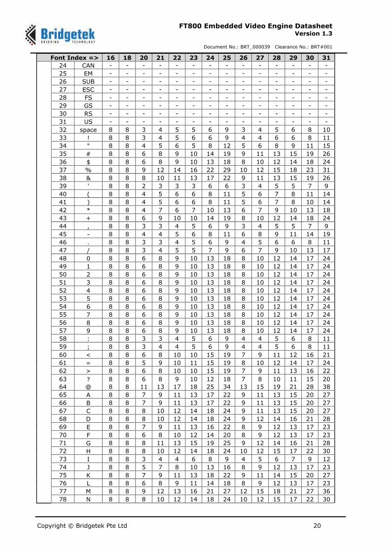
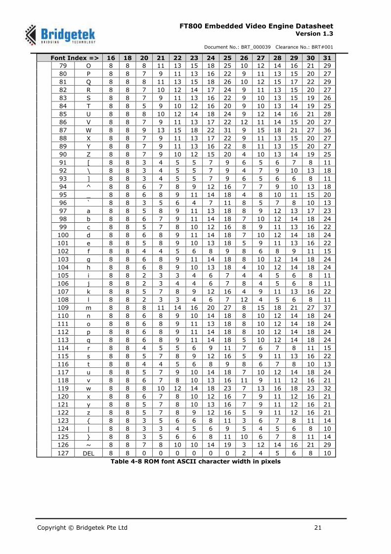
Table 4-8 ROM font ASCII character width in pixels
Copyright © Bridgetek Pte Ltd 22
FT800 Embedded Video Engine Datasheet Version 1.3
Document No.: BRT_000039 Clearance No.: BRT#001
Decim
al
Sym
bo
l
Decim
al
Sym
bo
l
Decim
al
Sym
bo
l
Decim
al
Sym
bo
l
Decim
al
Sym
bo
l
Decim
al
Sym
bo
l
Decim
al
Sym
bo
l
Decim
al
Sym
bo
l
128 Ç 144 É 160 á 176 192 208 ð 224 Ó 240 -
129 ü 145 æ 161 í 177 193 209 Ð 225 ß 241 ±
130 é 146 Æ 162 ó 178 194 210 Ê 226 Ô 242 ‗
131 â 147 ô 163 ú 179 195 211 Ë 227 Ò 243 ¾
132 ä 148 ö 164 ñ 180 196 212 È 228 õ 244 ¶
133 à 149 ò 165 Ñ 181 Á 197 213 ı 229 Õ 245 §
134 å 150 û 166 ª 182 Â 198 ã 214 Í 230 µ 246 ÷
135 ç 151 ù 167 º 183 À 199 Ã 215 Î 231 þ 247 ¸
136 ê 152 ÿ 168 ¿ 184 © 200 216 Ï 232 Þ 248 °
137 ë 153 Ö 169 ® 185 201 217 233 Ú 249 ¨
138 è 154 Ü 170 ¬ 186 202 218 234 Û 250 ·
139 ï 155 ø 171 ½ 187 203 219 235 Ù 251 ¹
140 î 156 £ 172 ¼ 188 204 220 236 ý 252 ³
141 ì 157 Ø 173 ¡ 189 ¢ 205 221 ¦ 237 Ý 253 ²
142 Ä 158 × 174 « 190 ¥ 206 222 Ì 238 ¯ 254
143 Å 159 ƒ 175 » 191 207 ¤ 223 239 ´ 255 nbsp
Table 4-9 ROM font Extended ASCII characters
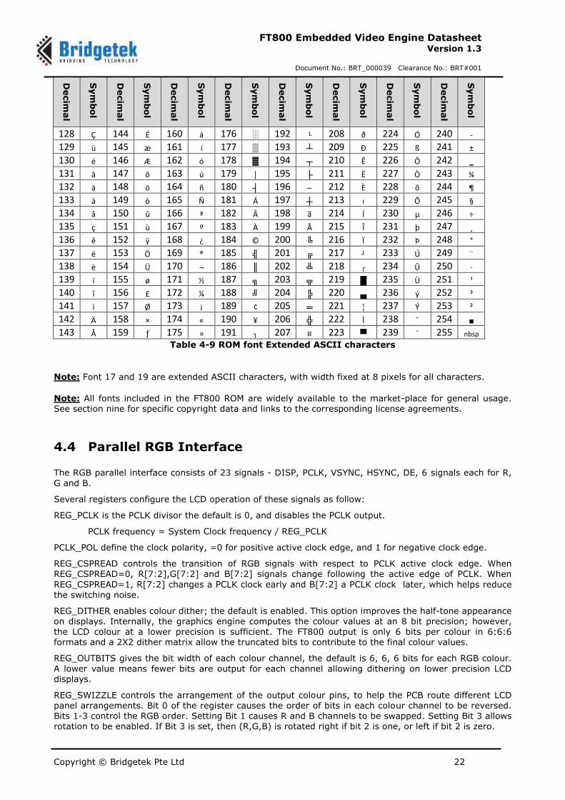
Note: Font 17 and 19 are extended ASCII characters, with width fixed at 8 pixels for all characters.
Note: All fonts included in the FT800 ROM are widely available to the market-place for general usage. See section nine for specific copyright data and links to the corresponding license agreements.
4.4 Parallel RGB Interface
The RGB parallel interface consists of 23 signals - DISP, PCLK, VSYNC, HSYNC, DE, 6 signals each for R,
G and B.
Several registers configure the LCD operation of these signals as follow:
REG_PCLK is the PCLK divisor the default is 0, and disables the PCLK output.
PCLK frequency = System Clock frequency / REG_PCLK
PCLK_POL define the clock polarity, =0 for positive active clock edge, and 1 for negative clock edge.
REG_CSPREAD controls the transition of RGB signals with respect to PCLK active clock edge. When REG_CSPREAD=0, R[7:2],G[7:2] and B[7:2] signals change following the active edge of PCLK. When
REG_CSPREAD=1, R[7:2] changes a PCLK clock early and B[7:2] a PCLK clock later, which helps reduce the switching noise.
REG_DITHER enables colour dither; the default is enabled. This option improves the half-tone appearance on displays. Internally, the graphics engine computes the colour values at an 8 bit precision; however,
the LCD colour at a lower precision is sufficient. The FT800 output is only 6 bits per colour in 6:6:6 formats and a 2X2 dither matrix allow the truncated bits to contribute to the final colour values.
REG_OUTBITS gives the bit width of each colour channel, the default is 6, 6, 6 bits for each RGB colour.
A lower value means fewer bits are output for each channel allowing dithering on lower precision LCD displays.
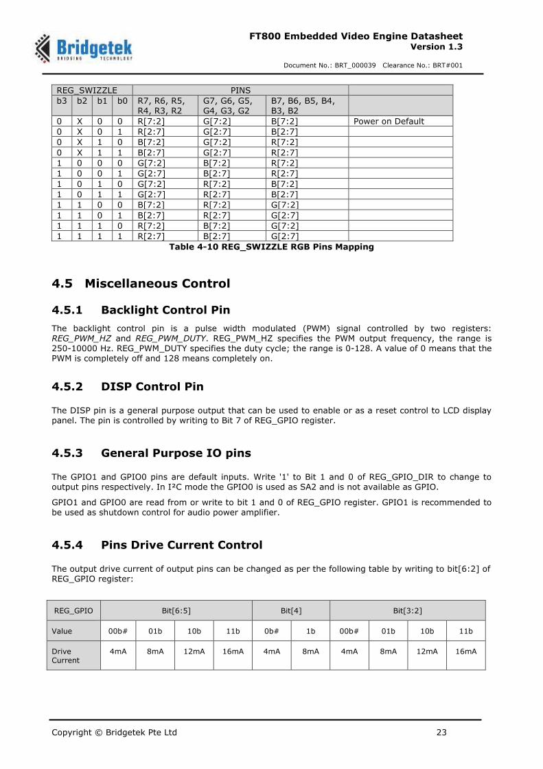
REG_SWIZZLE controls the arrangement of the output colour pins, to help the PCB route different LCD panel arrangements. Bit 0 of the register causes the order of bits in each colour channel to be reversed. Bits 1-3 control the RGB order. Setting Bit 1 causes R and B channels to be swapped. Setting Bit 3 allows rotation to be enabled. If Bit 3 is set, then (R,G,B) is rotated right if bit 2 is one, or left if bit 2 is zero.
Copyright © Bridgetek Pte Ltd 23
FT800 Embedded Video Engine Datasheet Version 1.3
Document No.: BRT_000039 Clearance No.: BRT#001
REG_SWIZZLE PINS
b3 b2 b1 b0 R7, R6, R5, R4, R3, R2
G7, G6, G5, G4, G3, G2
B7, B6, B5, B4, B3, B2
0 X 0 0 R[7:2] G[7:2] B[7:2] Power on Default
0 X 0 1 R[2:7] G[2:7] B[2:7]
0 X 1 0 B[7:2] G[7:2] R[7:2]
0 X 1 1 B[2:7] G[2:7] R[2:7]
1 0 0 0 G[7:2] B[7:2] R[7:2]
1 0 0 1 G[2:7] B[2:7] R[2:7]
1 0 1 0 G[7:2] R[7:2] B[7:2]
1 0 1 1 G[2:7] R[2:7] B[2:7]
1 1 0 0 B[7:2] R[7:2] G[7:2]
1 1 0 1 B[2:7] R[2:7] G[2:7]
1 1 1 0 R[7:2] B[7:2] G[7:2]
1 1 1 1 R[2:7] B[2:7] G[2:7]
Table 4-10 REG_SWIZZLE RGB Pins Mapping
4.5 Miscellaneous Control
4.5.1 Backlight Control Pin
The backlight control pin is a pulse width modulated (PWM) signal controlled by two registers: REG_PWM_HZ and REG_PWM_DUTY. REG_PWM_HZ specifies the PWM output frequency, the range is 250-10000 Hz. REG_PWM_DUTY specifies the duty cycle; the range is 0-128. A value of 0 means that the PWM is completely off and 128 means completely on.
4.5.2 DISP Control Pin
The DISP pin is a general purpose output that can be used to enable or as a reset control to LCD display panel. The pin is controlled by writing to Bit 7 of REG_GPIO register.
4.5.3 General Purpose IO pins
The GPIO1 and GPIO0 pins are default inputs. Write '1' to Bit 1 and 0 of REG_GPIO_DIR to change to output pins respectively. In I²C mode the GPIO0 is used as SA2 and is not available as GPIO.
GPIO1 and GPIO0 are read from or write to bit 1 and 0 of REG_GPIO register. GPIO1 is recommended to be used as shutdown control for audio power amplifier.
4.5.4 Pins Drive Current Control
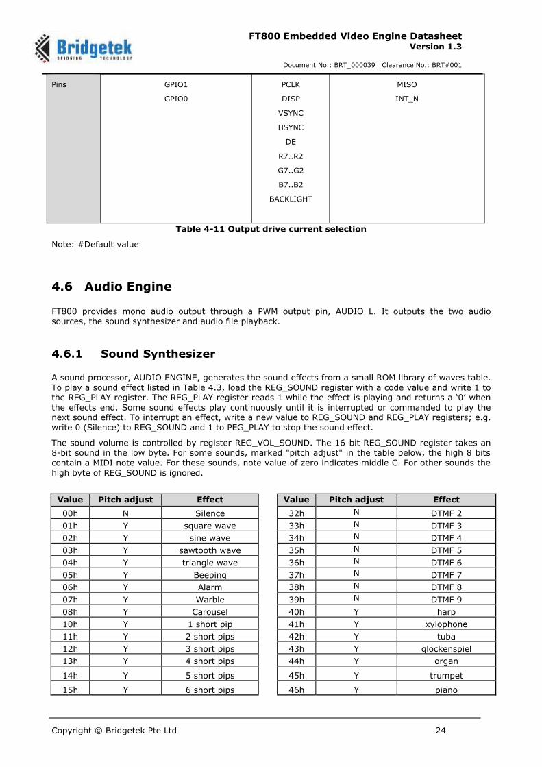
The output drive current of output pins can be changed as per the following table by writing to bit[6:2] of REG_GPIO register:
REG_GPIO Bit[6:5] Bit[4] Bit[3:2]
Value 00b# 01b 10b 11b 0b# 1b 00b# 01b 10b 11b
Drive Current
4mA 8mA 12mA 16mA 4mA 8mA 4mA 8mA 12mA 16mA
Copyright © Bridgetek Pte Ltd 24
FT800 Embedded Video Engine Datasheet Version 1.3
Document No.: BRT_000039 Clearance No.: BRT#001
Pins
GPIO1
GPIO0
PCLK
DISP
VSYNC
HSYNC
DE
R7..R2
G7..G2
B7..B2
BACKLIGHT
MISO
INT_N
Table 4-11 Output drive current selection
Note: #Default value
4.6 Audio Engine
FT800 provides mono audio output through a PWM output pin, AUDIO_L. It outputs the two audio
sources, the sound synthesizer and audio file playback.
4.6.1 Sound Synthesizer
A sound processor, AUDIO ENGINE, generates the sound effects from a small ROM library of waves table. To play a sound effect listed in Table 4.3, load the REG_SOUND register with a code value and write 1 to the REG_PLAY register. The REG_PLAY register reads 1 while the effect is playing and returns a ‘0’ when
the effects end. Some sound effects play continuously until it is interrupted or commanded to play the next sound effect. To interrupt an effect, write a new value to REG_SOUND and REG_PLAY registers; e.g.
write 0 (Silence) to REG_SOUND and 1 to PEG_PLAY to stop the sound effect.
The sound volume is controlled by register REG_VOL_SOUND. The 16-bit REG_SOUND register takes an 8-bit sound in the low byte. For some sounds, marked "pitch adjust" in the table below, the high 8 bits contain a MIDI note value. For these sounds, note value of zero indicates middle C. For other sounds the
high byte of REG_SOUND is ignored.
Value Pitch adjust Effect Value Pitch adjust Effect
00h N Silence 32h N DTMF 2
01h Y square wave 33h N DTMF 3
02h Y sine wave 34h N DTMF 4
03h Y sawtooth wave 35h N DTMF 5
04h Y triangle wave 36h N DTMF 6
05h Y Beeping 37h N DTMF 7
06h Y Alarm 38h N DTMF 8
07h Y Warble 39h N DTMF 9
08h Y Carousel 40h Y harp
10h Y 1 short pip 41h Y xylophone
11h Y 2 short pips 42h Y tuba
12h Y 3 short pips 43h Y glockenspiel
13h Y 4 short pips 44h Y organ
14h Y 5 short pips 45h Y trumpet
15h Y 6 short pips 46h Y piano
Copyright © Bridgetek Pte Ltd 25
FT800 Embedded Video Engine Datasheet Version 1.3
Document No.: BRT_000039 Clearance No.: BRT#001
16h Y 7 short pips 47h Y chimes
17h Y 8 short pips 48h Y music box
18h Y 9 short pips 49h Y bell
19h Y 10 short pips 50h N click
1Ah Y 11 short pips 51h N switch
1Bh Y 12 short pips 52h N cowbell
1Ch Y 13 short pips 53h N notch
1Dh Y 14 short pips 54h N hihat
1Eh Y 15 short pips 55h N kickdrum
1Fh Y 16 short pips 56h N pop
23h N DTMF # 57h N clack
2Ch N DTMF * 58h N chack
30h N DTMF 0 60h N mute
31h N DTMF 1 61h N unmute
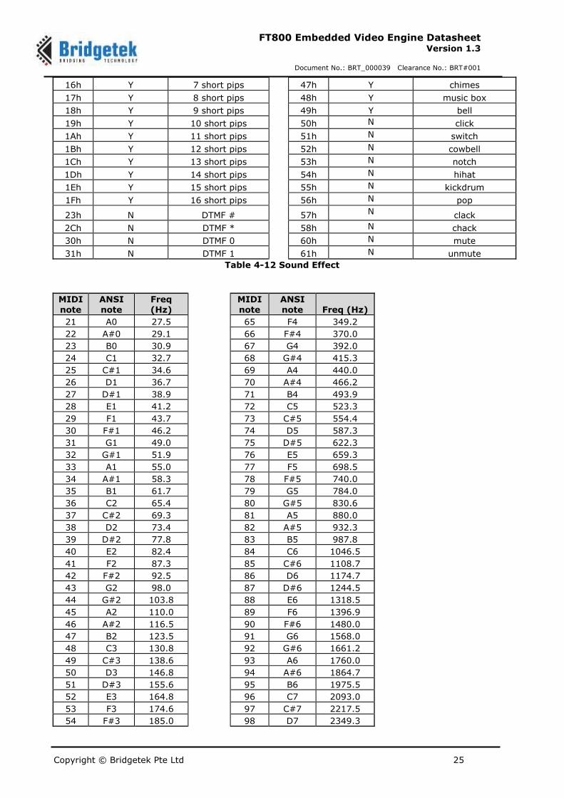
Table 4-12 Sound Effect
MIDI note
ANSI note
Freq (Hz)
MIDI note
ANSI note Freq (Hz)
21 A0 27.5 65 F4 349.2
22 A#0 29.1 66 F#4 370.0
23 B0 30.9 67 G4 392.0
24 C1 32.7 68 G#4 415.3
25 C#1 34.6 69 A4 440.0
26 D1 36.7 70 A#4 466.2
27 D#1 38.9 71 B4 493.9
28 E1 41.2 72 C5 523.3
29 F1 43.7 73 C#5 554.4
30 F#1 46.2 74 D5 587.3
31 G1 49.0 75 D#5 622.3
32 G#1 51.9 76 E5 659.3
33 A1 55.0 77 F5 698.5
34 A#1 58.3 78 F#5 740.0
35 B1 61.7 79 G5 784.0
36 C2 65.4 80 G#5 830.6
37 C#2 69.3 81 A5 880.0
38 D2 73.4 82 A#5 932.3
39 D#2 77.8 83 B5 987.8
40 E2 82.4 84 C6 1046.5
41 F2 87.3 85 C#6 1108.7
42 F#2 92.5 86 D6 1174.7
43 G2 98.0 87 D#6 1244.5
44 G#2 103.8 88 E6 1318.5
45 A2 110.0 89 F6 1396.9
46 A#2 116.5 90 F#6 1480.0
47 B2 123.5 91 G6 1568.0
48 C3 130.8 92 G#6 1661.2
49 C#3 138.6 93 A6 1760.0
50 D3 146.8 94 A#6 1864.7
51 D#3 155.6 95 B6 1975.5
52 E3 164.8 96 C7 2093.0
53 F3 174.6 97 C#7 2217.5
54 F#3 185.0 98 D7 2349.3
Copyright © Bridgetek Pte Ltd 26
FT800 Embedded Video Engine Datasheet Version 1.3
Document No.: BRT_000039 Clearance No.: BRT#001
55 G3 196.0 99 D#7 2489.0
56 G#3 207.7 100 E7 2637.0
57 A3 220.0 101 F7 2793.8
58 A#3 233.1 102 F#7 2960.0
59 B3 246.9 103 G7 3136.0
60 C4 261.6 104 G#7 3322.4
61 C#4 277.2 105 A7 3520.0
62 D4 293.7 106 A#7 3729.3
63 D#4 311.1 107 B7 3951.1
64 E4 329.6 108 C8 4186.0
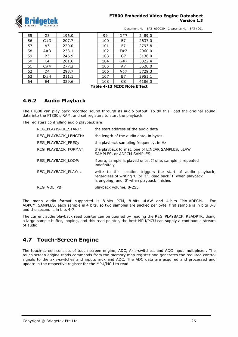
Table 4-13 MIDI Note Effect
4.6.2 Audio Playback
The FT800 can play back recorded sound through its audio output. To do this, load the original sound
data into the FT800’s RAM, and set registers to start the playback.
The registers controlling audio playback are:
REG_PLAYBACK_START: the start address of the audio data
REG_PLAYBACK_LENGTH: the length of the audio data, in bytes
REG_PLAYBACK_FREQ: the playback sampling frequency, in Hz
REG_PLAYBACK_FORMAT: the playback format, one of LINEAR SAMPLES, uLAW
SAMPLES, or ADPCM SAMPLES
REG_PLAYBACK_LOOP: if zero, sample is played once. If one, sample is repeated indefinitely
REG_PLAYBACK_PLAY: a write to this location triggers the start of audio playback, regardless of writing ‘0’ or ‘1’. Read back ‘1’ when playback is ongoing, and ‘0’ when playback finishes
REG_VOL_PB: playback volume, 0-255
The mono audio format supported is 8-bits PCM, 8-bits uLAW and 4-bits IMA-ADPCM. For ADPCM_SAMPLES, each sample is 4 bits, so two samples are packed per byte, first sample is in bits 0-3 and the second is in bits 4-7.
The current audio playback read pointer can be queried by reading the REG_PLAYBACK_READPTR. Using a large sample buffer, looping, and this read pointer, the host MPU/MCU can supply a continuous stream
of audio.
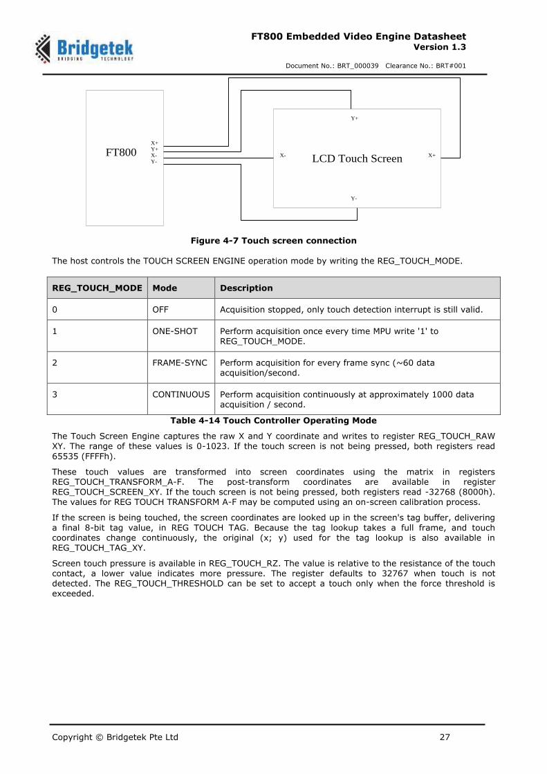
4.7 Touch-Screen Engine
The touch-screen consists of touch screen engine, ADC, Axis-switches, and ADC input multiplexer. The touch screen engine reads commands from the memory map register and generates the required control
signals to the axis-switches and inputs mux and ADC. The ADC data are acquired and processed and
update in the respective register for the MPU/MCU to read.
Copyright © Bridgetek Pte Ltd 27
FT800 Embedded Video Engine Datasheet Version 1.3
Document No.: BRT_000039 Clearance No.: BRT#001
Figure 4-7 Touch screen connection
The host controls the TOUCH SCREEN ENGINE operation mode by writing the REG_TOUCH_MODE.
REG_TOUCH_MODE Mode Description
0 OFF Acquisition stopped, only touch detection interrupt is still valid.
1 ONE-SHOT Perform acquisition once every time MPU write '1' to REG_TOUCH_MODE.
2 FRAME-SYNC Perform acquisition for every frame sync (~60 data acquisition/second.
3 CONTINUOUS Perform acquisition continuously at approximately 1000 data acquisition / second.
Table 4-14 Touch Controller Operating Mode
The Touch Screen Engine captures the raw X and Y coordinate and writes to register REG_TOUCH_RAW XY. The range of these values is 0-1023. If the touch screen is not being pressed, both registers read
65535 (FFFFh).
These touch values are transformed into screen coordinates using the matrix in registers REG_TOUCH_TRANSFORM_A-F. The post-transform coordinates are available in register REG_TOUCH_SCREEN_XY. If the touch screen is not being pressed, both registers read -32768 (8000h). The values for REG TOUCH TRANSFORM A-F may be computed using an on-screen calibration process.
If the screen is being touched, the screen coordinates are looked up in the screen's tag buffer, delivering
a final 8-bit tag value, in REG TOUCH TAG. Because the tag lookup takes a full frame, and touch coordinates change continuously, the original (x; y) used for the tag lookup is also available in REG_TOUCH_TAG_XY.
Screen touch pressure is available in REG_TOUCH_RZ. The value is relative to the resistance of the touch contact, a lower value indicates more pressure. The register defaults to 32767 when touch is not detected. The REG_TOUCH_THRESHOLD can be set to accept a touch only when the force threshold is exceeded.
Y+
Y-
X- X+FT800X+Y+X-Y- LCD Touch Screen
Copyright © Bridgetek Pte Ltd 28
FT800 Embedded Video Engine Datasheet Version 1.3
Document No.: BRT_000039 Clearance No.: BRT#001
4.8 Power Management
4.8.1 Power supply
The FT800 may be operated with a single supply of 3.3V apply to VCC and VCCIO pins. For operation with host MPU/MCU at lower supply, connect the VCCIO to MPU power to match the interface power.
Symbol Typical Description
VCCIO 1.8V, or 2.5V, or 3.3V Supply for Host interface digital I/O pad only, LCD RGB interface supply from VCC.
VCC 3.3V Supply for chip
Table 4-15 Power supply
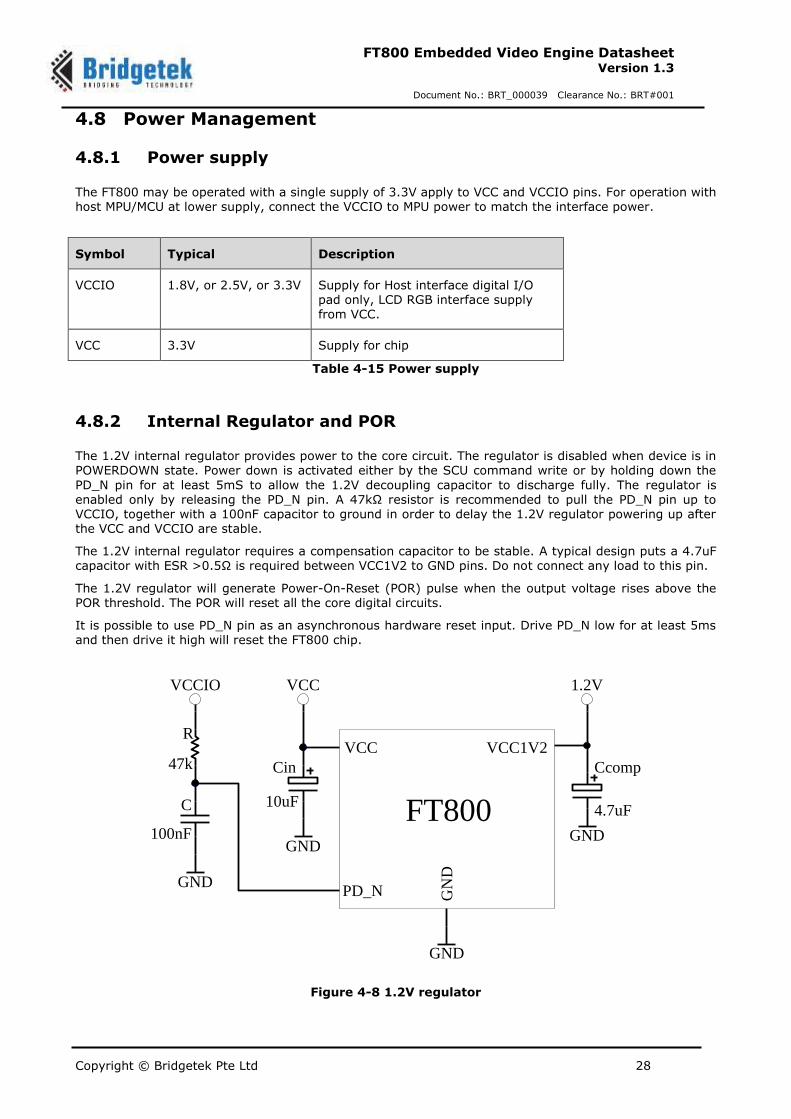
4.8.2 Internal Regulator and POR
The 1.2V internal regulator provides power to the core circuit. The regulator is disabled when device is in POWERDOWN state. Power down is activated either by the SCU command write or by holding down the
PD_N pin for at least 5mS to allow the 1.2V decoupling capacitor to discharge fully. The regulator is enabled only by releasing the PD_N pin. A 47kΩ resistor is recommended to pull the PD_N pin up to VCCIO, together with a 100nF capacitor to ground in order to delay the 1.2V regulator powering up after the VCC and VCCIO are stable.
The 1.2V internal regulator requires a compensation capacitor to be stable. A typical design puts a 4.7uF capacitor with ESR >0.5Ω is required between VCC1V2 to GND pins. Do not connect any load to this pin.
The 1.2V regulator will generate Power-On-Reset (POR) pulse when the output voltage rises above the POR threshold. The POR will reset all the core digital circuits.
It is possible to use PD_N pin as an asynchronous hardware reset input. Drive PD_N low for at least 5ms and then drive it high will reset the FT800 chip.
Figure 4-8 1.2V regulator
VCC
PD_N GN
D
VCC1V2
VCC
GND
GND
GND
VCCIO
C
R
Cin
10uF
100nF
1.2V
GND
Ccomp
4.7uF
47k
FT800
Copyright © Bridgetek Pte Ltd 29
FT800 Embedded Video Engine Datasheet Version 1.3
Document No.: BRT_000039 Clearance No.: BRT#001
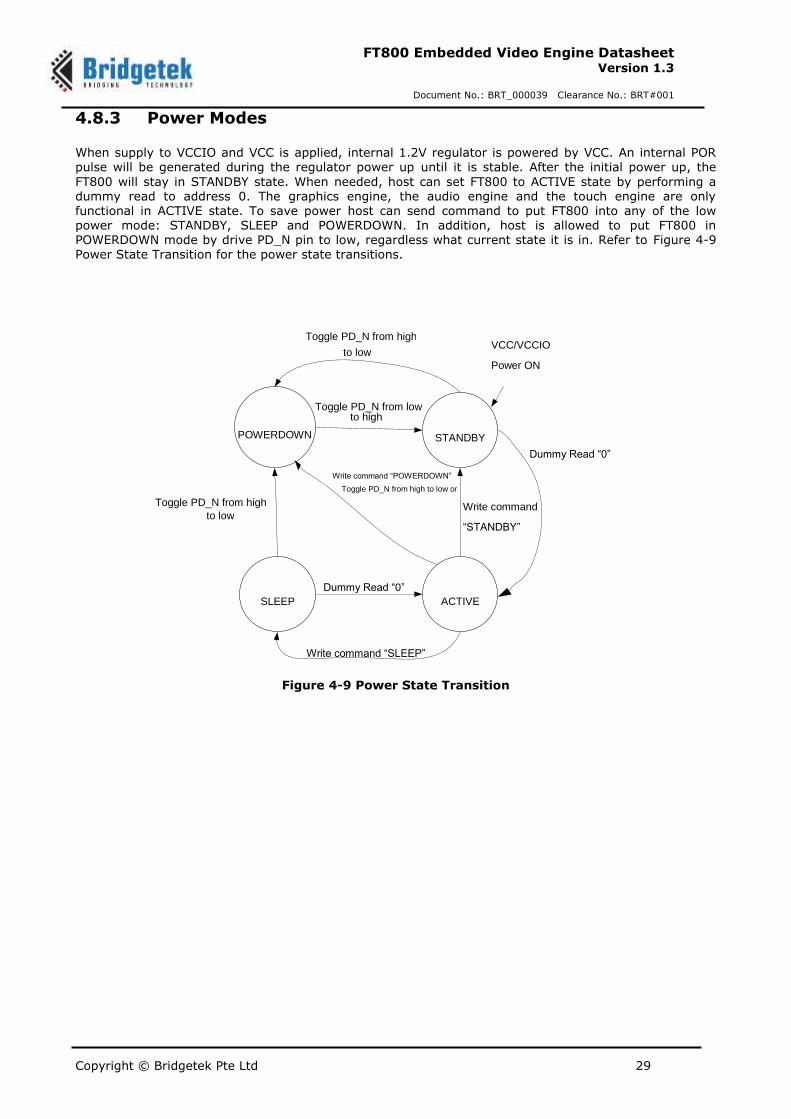
4.8.3 Power Modes
When supply to VCCIO and VCC is applied, internal 1.2V regulator is powered by VCC. An internal POR pulse will be generated during the regulator power up until it is stable. After the initial power up, the
FT800 will stay in STANDBY state. When needed, host can set FT800 to ACTIVE state by performing a dummy read to address 0. The graphics engine, the audio engine and the touch engine are only functional in ACTIVE state. To save power host can send command to put FT800 into any of the low power mode: STANDBY, SLEEP and POWERDOWN. In addition, host is allowed to put FT800 in POWERDOWN mode by drive PD_N pin to low, regardless what current state it is in. Refer to Figure 4-9 Power State Transition for the power state transitions.
Figure 4-9 Power State Transition
POWERDOWN STANDBY
SLEEP
VCC/VCCIO
Power ON
Toggle PD_N from high to low
ACTIVE
Toggle PD_N from low to high
Toggle PD_N from high
to low
Toggle PD_N from high to low or Write command “POWERDOWN”
Write command “SLEEP”
Write command
“STANDBY”
Dummy Read “0”
Dummy Read “ 0 ”
Copyright © Bridgetek Pte Ltd 30
FT800 Embedded Video Engine Datasheet Version 1.3
Document No.: BRT_000039 Clearance No.: BRT#001
4.8.3.1 ACTIVE state
In ACTIVE state, the FT800 is in normal operation. The crystal oscillator and PLL are functioning. The system clock applied to the FT800 core engines is enabled.
4.8.3.2 STANDBY state
In STANDBY state, the crystal oscillator and PLL remain functioning; the system clock applied to the FT800 core engines is disabled. All register contents are retained.
4.8.3.3 SLEEP state
In SLEEP state, the crystal oscillator, PLL and system clock applied to the FT800 core engines are disabled. All register contents are retained.
4.8.3.4 POWERDOWN state
In POWERDOWN state, the internal 1.2V regulator supplying the core digital logic, the crystal oscillator, the PLL and the system clock applied to the FT800 core is disabled. All register contents are lost and reset to default when the chip is next switched on.
4.8.3.5 Wake up to ACTIVE from other power states
Wake up from POWERDOWN state requires the host to pull the PD_N pin down and release, a low to high transition enables the 1.2V regulator. POR generated when 1.2V is stable and FT800 will switch to STANDBY mode after internal oscillator and PLL are up (maximum 20ms from PD_N rising edge). The clock enable sequence mentioned in section 4.2.3 shall be executed to proper enable the system clock.
From SLEEP state, host MPU reads at memory address 0 to wake the FT800 into ACTIVE state. Host needs to wait for at least 20ms before accessing any registers or commands. This is to guarantee the crystal oscillator and PLL are up and stable.
From STANDBY state, host MPU reads at memory address 0 to wake the FT800 into ACTIVE state. Host can immediately access any register or command.
4.8.3.6 Pin Status at Different Power States
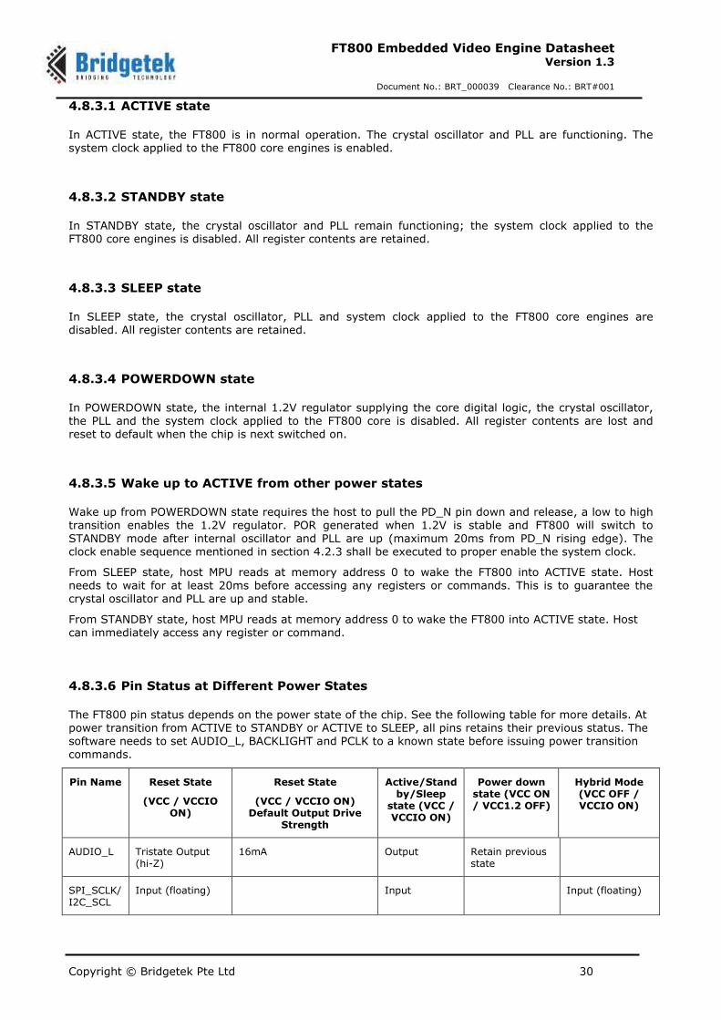
The FT800 pin status depends on the power state of the chip. See the following table for more details. At power transition from ACTIVE to STANDBY or ACTIVE to SLEEP, all pins retains their previous status. The software needs to set AUDIO_L, BACKLIGHT and PCLK to a known state before issuing power transition commands.
Pin Name Reset State
(VCC / VCCIO ON)
Reset State
(VCC / VCCIO ON) Default Output Drive
Strength
Active/Standby/Sleep
state (VCC / VCCIO ON)
Power down state (VCC ON / VCC1.2 OFF)
Hybrid Mode (VCC OFF / VCCIO ON)
AUDIO_L Tristate Output (hi-Z)
16mA Output Retain previous state
SPI_SCLK/I2C_SCL
Input (floating) Input Input (floating)
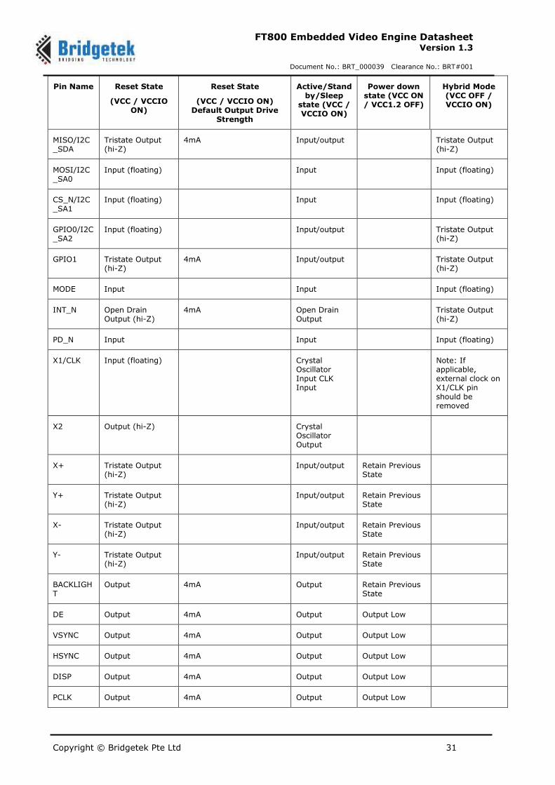
Copyright © Bridgetek Pte Ltd 31
FT800 Embedded Video Engine Datasheet Version 1.3
Document No.: BRT_000039 Clearance No.: BRT#001
Pin Name Reset State
(VCC / VCCIO ON)
Reset State
(VCC / VCCIO ON) Default Output Drive
Strength
Active/Standby/Sleep
state (VCC / VCCIO ON)
Power down state (VCC ON / VCC1.2 OFF)
Hybrid Mode (VCC OFF / VCCIO ON)
MISO/I2C_SDA
Tristate Output (hi-Z)
4mA Input/output Tristate Output (hi-Z)
MOSI/I2C_SA0
Input (floating) Input Input (floating)
CS_N/I2C_SA1
Input (floating) Input Input (floating)
GPIO0/I2C_SA2
Input (floating) Input/output Tristate Output (hi-Z)
GPIO1 Tristate Output (hi-Z)
4mA Input/output Tristate Output (hi-Z)
MODE Input Input Input (floating)
INT_N Open Drain Output (hi-Z)
4mA Open Drain Output
Tristate Output (hi-Z)
PD_N Input Input Input (floating)
X1/CLK Input (floating) Crystal Oscillator Input CLK Input
Note: If applicable, external clock on X1/CLK pin should be removed
X2 Output (hi-Z) Crystal Oscillator Output
X+ Tristate Output (hi-Z)
Input/output Retain Previous State
Y+ Tristate Output (hi-Z)
Input/output Retain Previous State
X- Tristate Output (hi-Z)
Input/output Retain Previous State
Y- Tristate Output (hi-Z)
Input/output Retain Previous State
BACKLIGHT
Output 4mA Output Retain Previous State
DE Output 4mA Output Output Low
VSYNC Output 4mA Output Output Low
HSYNC Output 4mA Output Output Low
DISP Output 4mA Output Output Low
PCLK Output 4mA Output Output Low
Copyright © Bridgetek Pte Ltd 32
FT800 Embedded Video Engine Datasheet Version 1.3
Document No.: BRT_000039 Clearance No.: BRT#001
Pin Name Reset State
(VCC / VCCIO ON)
Reset State
(VCC / VCCIO ON) Default Output Drive
Strength
Active/Standby/Sleep
state (VCC / VCCIO ON)
Power down state (VCC ON / VCC1.2 OFF)
Hybrid Mode (VCC OFF / VCCIO ON)
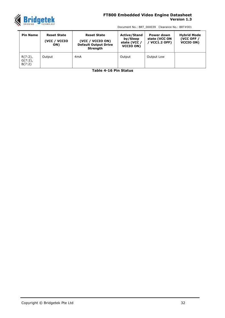
R(7:2), G(7:2), B(7:2)
Output 4mA Output Output Low
Table 4-16 Pin Status
Copyright © Bridgetek Pte Ltd 33
FT800 Embedded Video Engine Datasheet Version 1.3
Document No.: BRT_000039 Clearance No.: BRT#001
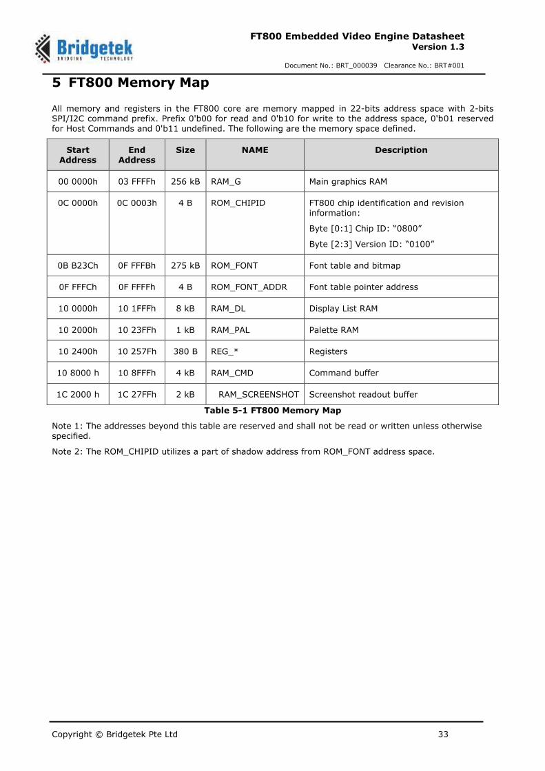
5 FT800 Memory Map
All memory and registers in the FT800 core are memory mapped in 22-bits address space with 2-bits SPI/I2C command prefix. Prefix 0'b00 for read and 0'b10 for write to the address space, 0'b01 reserved for Host Commands and 0'b11 undefined. The following are the memory space defined.
Start Address
End Address
Size NAME Description
00 0000h 03 FFFFh 256 kB RAM_G Main graphics RAM
0C 0000h 0C 0003h 4 B ROM_CHIPID FT800 chip identification and revision information:
Byte [0:1] Chip ID: “0800”
Byte [2:3] Version ID: “0100”
0B B23Ch 0F FFFBh 275 kB ROM_FONT Font table and bitmap
0F FFFCh 0F FFFFh 4 B ROM_FONT_ADDR Font table pointer address
10 0000h 10 1FFFh 8 kB RAM_DL Display List RAM
10 2000h 10 23FFh 1 kB RAM_PAL Palette RAM
10 2400h 10 257Fh 380 B REG_* Registers
10 8000 h 10 8FFFh 4 kB RAM_CMD Command buffer
1C 2000 h 1C 27FFh 2 kB RAM_SCREENSHOT Screenshot readout buffer
Table 5-1 FT800 Memory Map
Note 1: The addresses beyond this table are reserved and shall not be read or written unless otherwise
specified.
Note 2: The ROM_CHIPID utilizes a part of shadow address from ROM_FONT address space.
Copyright © Bridgetek Pte Ltd 34
FT800 Embedded Video Engine Datasheet Version 1.3
Document No.: BRT_000039 Clearance No.: BRT#001
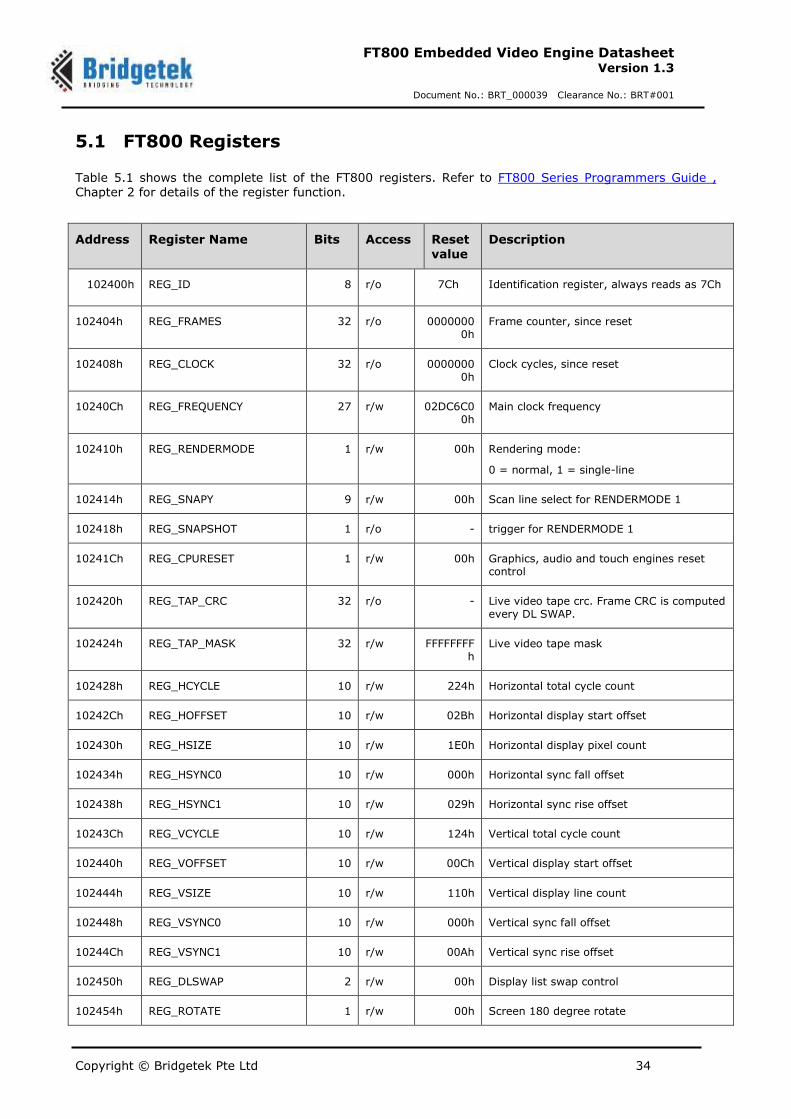
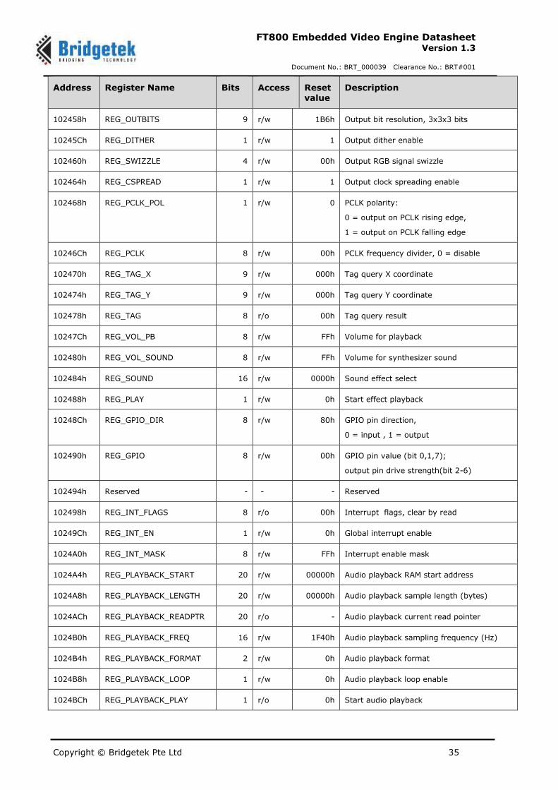
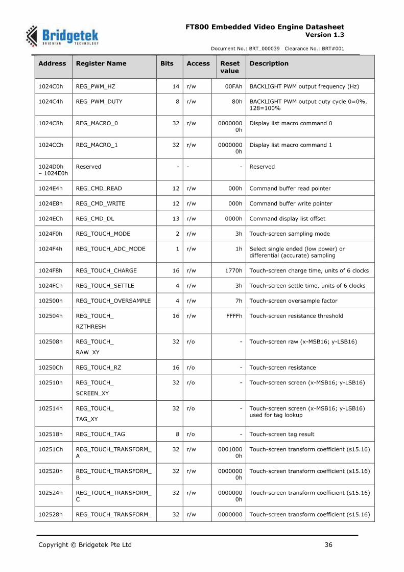
5.1 FT800 Registers
Table 5.1 shows the complete list of the FT800 registers. Refer to FT800 Series Programmers Guide , Chapter 2 for details of the register function.
Address Register Name Bits Access Reset
value
Description
102400h REG_ID 8 r/o 7Ch Identification register, always reads as 7Ch
102404h REG_FRAMES 32 r/o 00000000h
Frame counter, since reset
102408h REG_CLOCK 32 r/o 00000000h
Clock cycles, since reset
10240Ch REG_FREQUENCY 27 r/w 02DC6C00h
Main clock frequency
102410h REG_RENDERMODE 1 r/w 00h Rendering mode:
0 = normal, 1 = single-line
102414h REG_SNAPY 9 r/w 00h Scan line select for RENDERMODE 1
102418h REG_SNAPSHOT 1 r/o - trigger for RENDERMODE 1
10241Ch REG_CPURESET 1 r/w 00h Graphics, audio and touch engines reset control
102420h REG_TAP_CRC 32 r/o - Live video tape crc. Frame CRC is computed every DL SWAP.
102424h REG_TAP_MASK 32 r/w FFFFFFFFh
Live video tape mask
102428h REG_HCYCLE 10 r/w 224h Horizontal total cycle count
10242Ch REG_HOFFSET 10 r/w 02Bh Horizontal display start offset
102430h REG_HSIZE 10 r/w 1E0h Horizontal display pixel count
102434h REG_HSYNC0 10 r/w 000h Horizontal sync fall offset
102438h REG_HSYNC1 10 r/w 029h Horizontal sync rise offset
10243Ch REG_VCYCLE 10 r/w 124h Vertical total cycle count
102440h REG_VOFFSET 10 r/w 00Ch Vertical display start offset
102444h REG_VSIZE 10 r/w 110h Vertical display line count
102448h REG_VSYNC0 10 r/w 000h Vertical sync fall offset
10244Ch REG_VSYNC1 10 r/w 00Ah Vertical sync rise offset
102450h REG_DLSWAP 2 r/w 00h Display list swap control
102454h REG_ROTATE 1 r/w 00h Screen 180 degree rotate
Copyright © Bridgetek Pte Ltd 35
FT800 Embedded Video Engine Datasheet Version 1.3
Document No.: BRT_000039 Clearance No.: BRT#001
Address Register Name Bits Access Reset value
Description
102458h REG_OUTBITS 9 r/w 1B6h Output bit resolution, 3x3x3 bits
10245Ch REG_DITHER 1 r/w 1 Output dither enable
102460h REG_SWIZZLE 4 r/w 00h Output RGB signal swizzle
102464h REG_CSPREAD 1 r/w 1 Output clock spreading enable
102468h REG_PCLK_POL 1 r/w 0 PCLK polarity:
0 = output on PCLK rising edge,
1 = output on PCLK falling edge
10246Ch REG_PCLK 8 r/w 00h PCLK frequency divider, 0 = disable
102470h REG_TAG_X 9 r/w 000h Tag query X coordinate
102474h REG_TAG_Y 9 r/w 000h Tag query Y coordinate
102478h REG_TAG 8 r/o 00h Tag query result
10247Ch REG_VOL_PB 8 r/w FFh Volume for playback
102480h REG_VOL_SOUND 8 r/w FFh Volume for synthesizer sound
102484h REG_SOUND 16 r/w 0000h Sound effect select
102488h REG_PLAY 1 r/w 0h Start effect playback
10248Ch REG_GPIO_DIR 8 r/w 80h GPIO pin direction,
0 = input , 1 = output
102490h REG_GPIO 8 r/w 00h GPIO pin value (bit 0,1,7);
output pin drive strength(bit 2-6)
102494h Reserved - - - Reserved
102498h REG_INT_FLAGS 8 r/o 00h Interrupt flags, clear by read
10249Ch REG_INT_EN 1 r/w 0h Global interrupt enable
1024A0h REG_INT_MASK 8 r/w FFh Interrupt enable mask
1024A4h REG_PLAYBACK_START 20 r/w 00000h Audio playback RAM start address
1024A8h REG_PLAYBACK_LENGTH 20 r/w 00000h Audio playback sample length (bytes)
1024ACh REG_PLAYBACK_READPTR 20 r/o - Audio playback current read pointer
1024B0h REG_PLAYBACK_FREQ 16 r/w 1F40h Audio playback sampling frequency (Hz)
1024B4h REG_PLAYBACK_FORMAT 2 r/w 0h Audio playback format
1024B8h REG_PLAYBACK_LOOP 1 r/w 0h Audio playback loop enable
1024BCh REG_PLAYBACK_PLAY 1 r/o 0h Start audio playback
Copyright © Bridgetek Pte Ltd 36
FT800 Embedded Video Engine Datasheet Version 1.3
Document No.: BRT_000039 Clearance No.: BRT#001
Address Register Name Bits Access Reset value
Description
1024C0h REG_PWM_HZ 14 r/w 00FAh BACKLIGHT PWM output frequency (Hz)
1024C4h REG_PWM_DUTY 8 r/w 80h BACKLIGHT PWM output duty cycle 0=0%, 128=100%
1024C8h REG_MACRO_0 32 r/w 00000000h
Display list macro command 0
1024CCh REG_MACRO_1 32 r/w 00000000h
Display list macro command 1
1024D0h – 1024E0h
Reserved - - - Reserved
1024E4h REG_CMD_READ 12 r/w 000h Command buffer read pointer
1024E8h REG_CMD_WRITE 12 r/w 000h Command buffer write pointer
1024ECh REG_CMD_DL 13 r/w 0000h Command display list offset
1024F0h REG_TOUCH_MODE 2 r/w 3h Touch-screen sampling mode
1024F4h REG_TOUCH_ADC_MODE 1 r/w 1h Select single ended (low power) or differential (accurate) sampling
1024F8h REG_TOUCH_CHARGE 16 r/w 1770h Touch-screen charge time, units of 6 clocks
1024FCh REG_TOUCH_SETTLE 4 r/w 3h Touch-screen settle time, units of 6 clocks
102500h REG_TOUCH_OVERSAMPLE 4 r/w 7h Touch-screen oversample factor
102504h REG_TOUCH_
RZTHRESH
16 r/w FFFFh Touch-screen resistance threshold
102508h REG_TOUCH_
RAW_XY
32 r/o - Touch-screen raw (x-MSB16; y-LSB16)
10250Ch REG_TOUCH_RZ 16 r/o - Touch-screen resistance
102510h REG_TOUCH_
SCREEN_XY
32 r/o - Touch-screen screen (x-MSB16; y-LSB16)
102514h REG_TOUCH_
TAG_XY
32 r/o - Touch-screen screen (x-MSB16; y-LSB16) used for tag lookup
102518h REG_TOUCH_TAG 8 r/o - Touch-screen tag result
10251Ch REG_TOUCH_TRANSFORM_A
32 r/w 00010000h
Touch-screen transform coefficient (s15.16)
102520h REG_TOUCH_TRANSFORM_B
32 r/w 00000000h
Touch-screen transform coefficient (s15.16)
102524h REG_TOUCH_TRANSFORM_C
32 r/w 00000000h
Touch-screen transform coefficient (s15.16)
102528h REG_TOUCH_TRANSFORM_ 32 r/w 0000000 Touch-screen transform coefficient (s15.16)
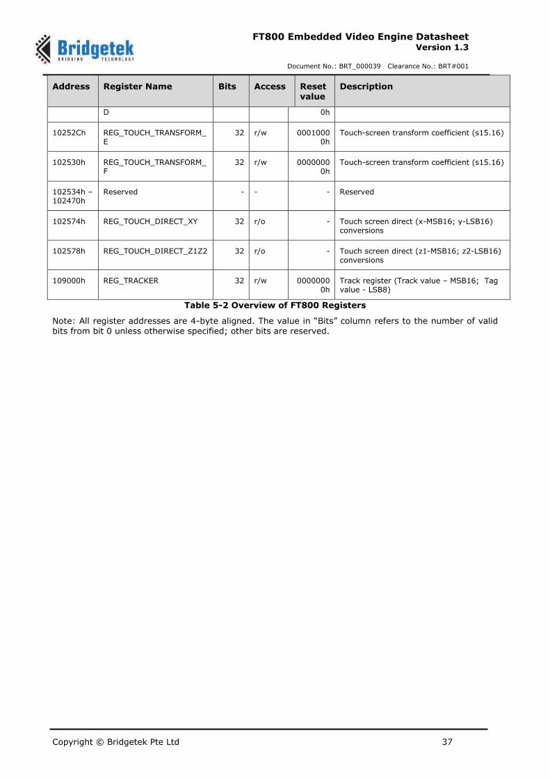
Copyright © Bridgetek Pte Ltd 37
FT800 Embedded Video Engine Datasheet Version 1.3
Document No.: BRT_000039 Clearance No.: BRT#001
Address Register Name Bits Access Reset value
Description
D 0h
10252Ch REG_TOUCH_TRANSFORM_E
32 r/w 00010000h
Touch-screen transform coefficient (s15.16)
102530h REG_TOUCH_TRANSFORM_F
32 r/w 00000000h
Touch-screen transform coefficient (s15.16)
102534h – 102470h
Reserved - - - Reserved
102574h REG_TOUCH_DIRECT_XY 32 r/o - Touch screen direct (x-MSB16; y-LSB16) conversions
102578h REG_TOUCH_DIRECT_Z1Z2 32 r/o - Touch screen direct (z1-MSB16; z2-LSB16) conversions
109000h REG_TRACKER 32 r/w 00000000h
Track register (Track value – MSB16; Tag value - LSB8)
Table 5-2 Overview of FT800 Registers
Note: All register addresses are 4-byte aligned. The value in “Bits” column refers to the number of valid bits from bit 0 unless otherwise specified; other bits are reserved.
Copyright © Bridgetek Pte Ltd 38
FT800 Embedded Video Engine Datasheet Version 1.3
Document No.: BRT_000039 Clearance No.: BRT#001
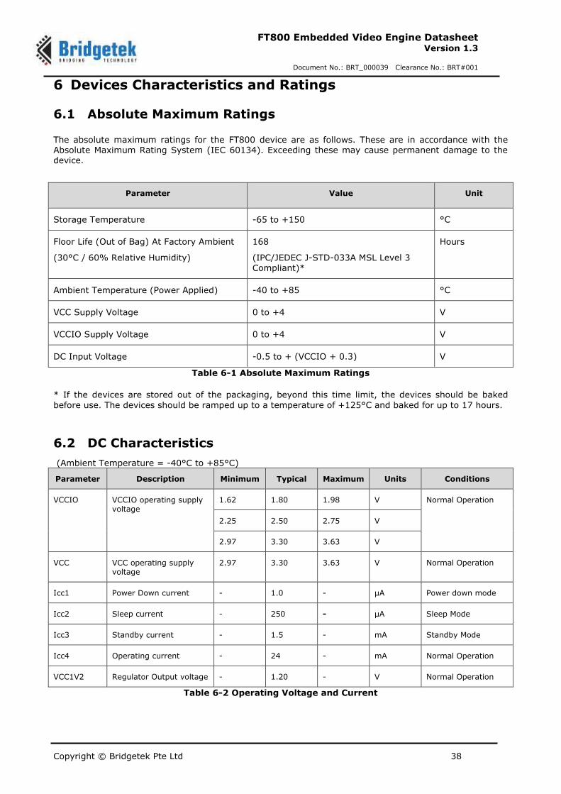
6 Devices Characteristics and Ratings
6.1 Absolute Maximum Ratings
The absolute maximum ratings for the FT800 device are as follows. These are in accordance with the Absolute Maximum Rating System (IEC 60134). Exceeding these may cause permanent damage to the device.
Parameter Value Unit
Storage Temperature -65 to +150 °C
Floor Life (Out of Bag) At Factory Ambient
(30°C / 60% Relative Humidity)
168
(IPC/JEDEC J-STD-033A MSL Level 3
Compliant)*
Hours
Ambient Temperature (Power Applied) -40 to +85 °C
VCC Supply Voltage 0 to +4 V
VCCIO Supply Voltage 0 to +4 V
DC Input Voltage -0.5 to + (VCCIO + 0.3) V
Table 6-1 Absolute Maximum Ratings
* If the devices are stored out of the packaging, beyond this time limit, the devices should be baked
before use. The devices should be ramped up to a temperature of +125°C and baked for up to 17 hours.
6.2 DC Characteristics
(Ambient Temperature = -40°C to +85°C)
Parameter Description Minimum Typical Maximum Units Conditions
VCCIO VCCIO operating supply voltage
1.62 1.80 1.98 V Normal Operation
2.25 2.50 2.75 V
2.97 3.30 3.63 V
VCC VCC operating supply voltage
2.97 3.30 3.63 V Normal Operation
Icc1 Power Down current - 1.0 - µA Power down mode
Icc2 Sleep current - 250 - µA Sleep Mode
Icc3 Standby current - 1.5 - mA Standby Mode
Icc4 Operating current - 24 - mA Normal Operation
VCC1V2 Regulator Output voltage - 1.20 - V Normal Operation
Table 6-2 Operating Voltage and Current
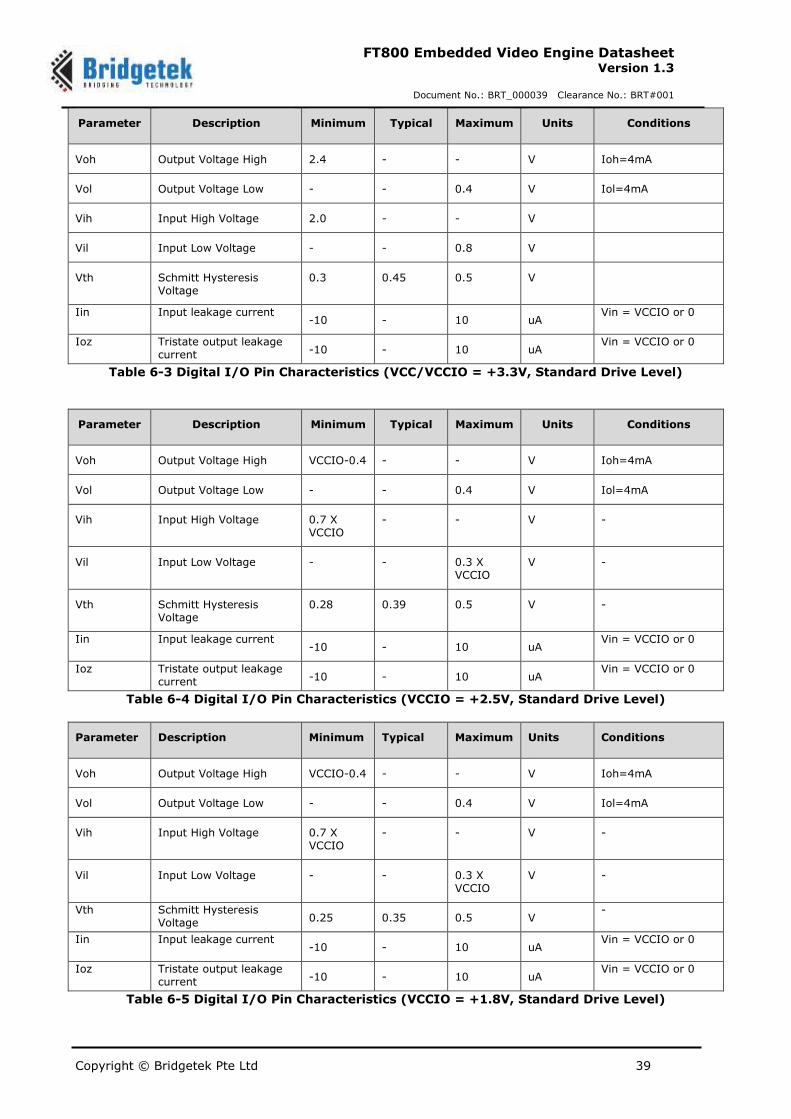
Copyright © Bridgetek Pte Ltd 39
FT800 Embedded Video Engine Datasheet Version 1.3
Document No.: BRT_000039 Clearance No.: BRT#001
Parameter Description Minimum Typical Maximum Units Conditions
Voh Output Voltage High 2.4 - - V Ioh=4mA
Vol Output Voltage Low - - 0.4 V Iol=4mA
Vih Input High Voltage 2.0 - - V
Vil Input Low Voltage - - 0.8 V
Vth Schmitt Hysteresis Voltage
0.3 0.45 0.5 V
Iin Input leakage current -10 - 10 uA
Vin = VCCIO or 0
Ioz Tristate output leakage current -10 - 10 uA
Vin = VCCIO or 0
Table 6-3 Digital I/O Pin Characteristics (VCC/VCCIO = +3.3V, Standard Drive Level)
Parameter Description Minimum Typical Maximum Units Conditions
Voh Output Voltage High VCCIO-0.4 - - V Ioh=4mA
Vol Output Voltage Low - - 0.4 V Iol=4mA
Vih Input High Voltage 0.7 X VCCIO
- - V -
Vil Input Low Voltage - - 0.3 X VCCIO
V -
Vth Schmitt Hysteresis Voltage
0.28 0.39 0.5 V -
Iin Input leakage current -10 - 10 uA
Vin = VCCIO or 0
Ioz Tristate output leakage current -10 - 10 uA
Vin = VCCIO or 0
Table 6-4 Digital I/O Pin Characteristics (VCCIO = +2.5V, Standard Drive Level)
Parameter Description Minimum Typical Maximum Units Conditions
Voh Output Voltage High VCCIO-0.4 - - V Ioh=4mA
Vol Output Voltage Low - - 0.4 V Iol=4mA
Vih Input High Voltage 0.7 X VCCIO
- - V -
Vil Input Low Voltage - - 0.3 X VCCIO
V -
Vth Schmitt Hysteresis Voltage 0.25 0.35 0.5 V
-
Iin Input leakage current -10 - 10 uA
Vin = VCCIO or 0
Ioz Tristate output leakage current -10 - 10 uA
Vin = VCCIO or 0
Table 6-5 Digital I/O Pin Characteristics (VCCIO = +1.8V, Standard Drive Level)
Copyright © Bridgetek Pte Ltd 40
FT800 Embedded Video Engine Datasheet Version 1.3
Document No.: BRT_000039 Clearance No.: BRT#001
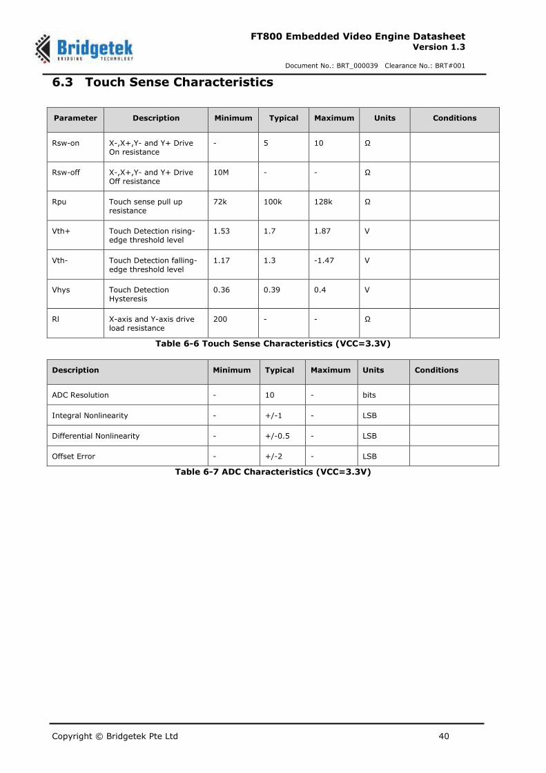
6.3 Touch Sense Characteristics
Parameter Description Minimum Typical Maximum Units Conditions
Rsw-on X-,X+,Y- and Y+ Drive On resistance
- 5 10 Ω
Rsw-off X-,X+,Y- and Y+ Drive Off resistance
10M - - Ω
Rpu Touch sense pull up resistance
72k 100k 128k Ω
Vth+ Touch Detection rising-edge threshold level
1.53 1.7 1.87 V
Vth- Touch Detection falling-
edge threshold level
1.17 1.3 -1.47 V
Vhys Touch Detection Hysteresis
0.36 0.39 0.4 V
Rl X-axis and Y-axis drive load resistance
200 - - Ω
Table 6-6 Touch Sense Characteristics (VCC=3.3V)
Description Minimum Typical Maximum Units Conditions
ADC Resolution - 10 - bits
Integral Nonlinearity - +/-1 - LSB
Differential Nonlinearity - +/-0.5 - LSB
Offset Error - +/-2 - LSB
Table 6-7 ADC Characteristics (VCC=3.3V)
Copyright © Bridgetek Pte Ltd 41
FT800 Embedded Video Engine Datasheet Version 1.3
Document No.: BRT_000039 Clearance No.: BRT#001
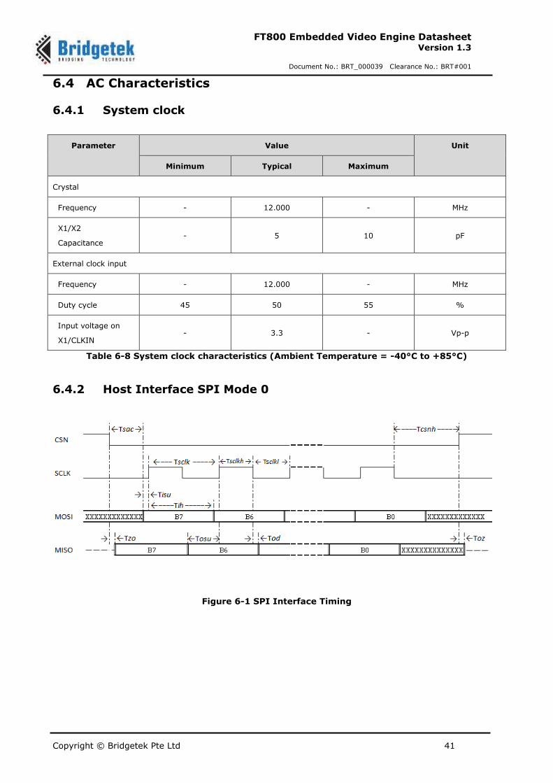
6.4 AC Characteristics
6.4.1 System clock
Parameter Value Unit
Minimum Typical Maximum
Crystal
Frequency - 12.000 - MHz
X1/X2
Capacitance - 5 10 pF
External clock input
Frequency - 12.000 - MHz
Duty cycle 45 50 55 %
Input voltage on
X1/CLKIN - 3.3 - Vp-p
Table 6-8 System clock characteristics (Ambient Temperature = -40°C to +85°C)
6.4.2 Host Interface SPI Mode 0
Figure 6-1 SPI Interface Timing

Copyright © Bridgetek Pte Ltd 42
FT800 Embedded Video Engine Datasheet Version 1.3
Document No.: BRT_000039 Clearance No.: BRT#001
Parameter
Description VCC(I/O)=1.8V VCC(I/O)=2.5V VCC(I/O)=3.3V Unit
Min Max Min Max Min Max
Fsclk SPI Clock frequency 0 25 0 30 0 30 Mhz
Tsclk SPI clock period 40 - 33 - 33 - ns
Tsclkl SPI clock low
duration
16 - 13 - 13 - ns
Tsclkh SPI clock high duration
16 - 13 - 13 - ns
Tsac SPI access time 10 - 10 - 10 - ns
Tisu Input Setup 5 - 5 - 5 - ns
Tih Input Hold 10 - 10 - 10 - ns
Tzo Output enable delay 5 10 5 10 5 10 ns
Toz Output disable delay 5 10 5 10 5 10 ns
Tosu Output setup time Tsclkl-5 - Tsclkl-5 - Tsclkl-5 - ns
Tod Output data delay 5 10 5 10 5 10 ns
Tcsnh CSN hold time 15 - 15 - 15 - ns
Table 6-9 SPI Interface Timing Specification
6.4.3 Host Interface I2C Mode Timing
Parameter
Description
Standard-
mode
Fast-mode Fast-plus
mode
High speed
mode
Unit
Min Max Min Max Min Max Min Max
Fscl I2C SCL clock frequency
0 100 0 400 0 1000 0 3400 kHz
Tscll clock low period 4.7 - 1.3 - 0.5 - 0.16 - µs
Tsclh clock high period 4.0 - 0.6 - 0.26 - 0.06 - µs
Tsu Data setup time 250 - 100 - 50 - 10 - ns
Thd Data hold time 0 - 0 - 0 - 0 70 ns
Tr Rise time - 1000 - 300 - 120 10 40 ns
Tf Fall time - 300 - 300 - 120 10 40 ns
Table 6-10 I2C Interface Timing
Copyright © Bridgetek Pte Ltd 43
FT800 Embedded Video Engine Datasheet Version 1.3
Document No.: BRT_000039 Clearance No.: BRT#001
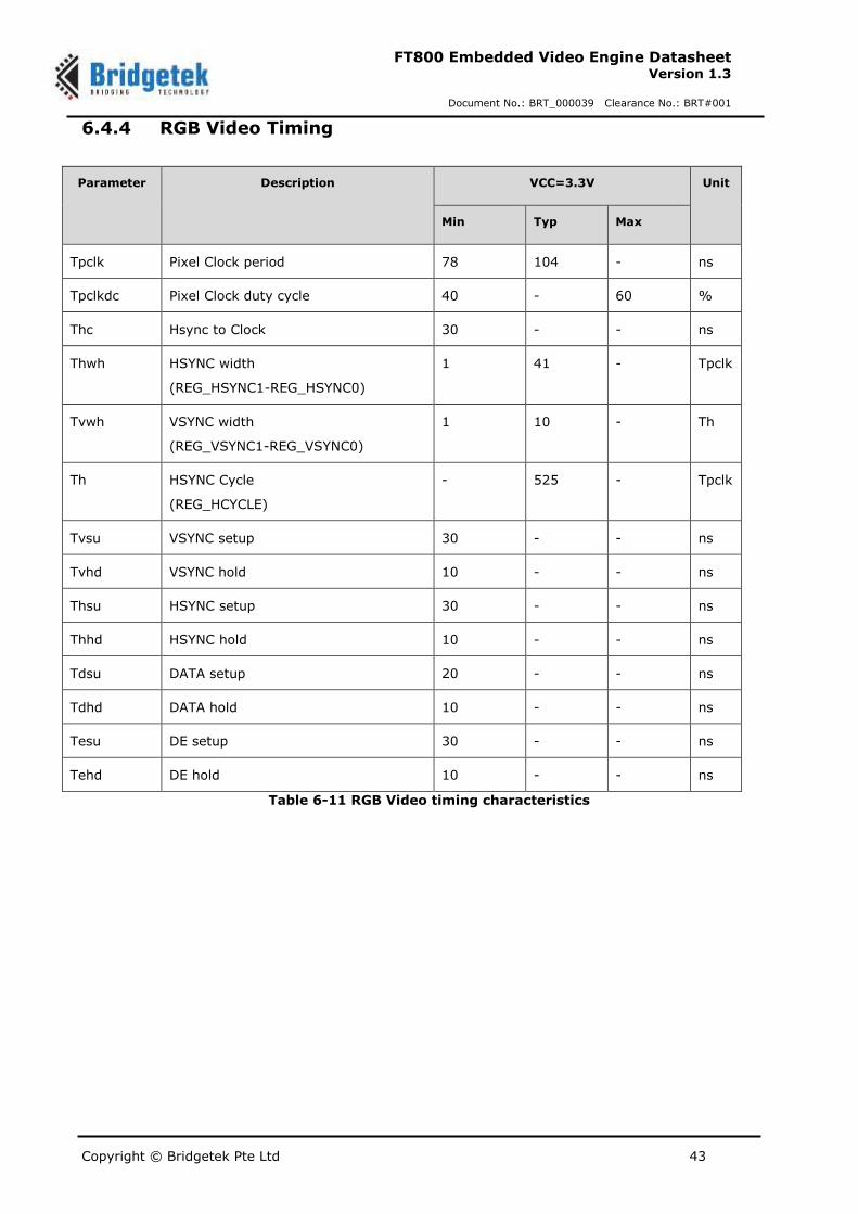
6.4.4 RGB Video Timing
Parameter Description VCC=3.3V Unit
Min Typ Max
Tpclk Pixel Clock period 78 104 - ns
Tpclkdc Pixel Clock duty cycle 40 - 60 %
Thc Hsync to Clock 30 - - ns
Thwh HSYNC width
(REG_HSYNC1-REG_HSYNC0)
1 41 - Tpclk
Tvwh VSYNC width
(REG_VSYNC1-REG_VSYNC0)
1 10 - Th
Th HSYNC Cycle
(REG_HCYCLE)
- 525 - Tpclk
Tvsu VSYNC setup 30 - - ns
Tvhd VSYNC hold 10 - - ns
Thsu HSYNC setup 30 - - ns
Thhd HSYNC hold 10 - - ns
Tdsu DATA setup 20 - - ns
Tdhd DATA hold 10 - - ns
Tesu DE setup 30 - - ns
Tehd DE hold 10 - - ns
Table 6-11 RGB Video timing characteristics
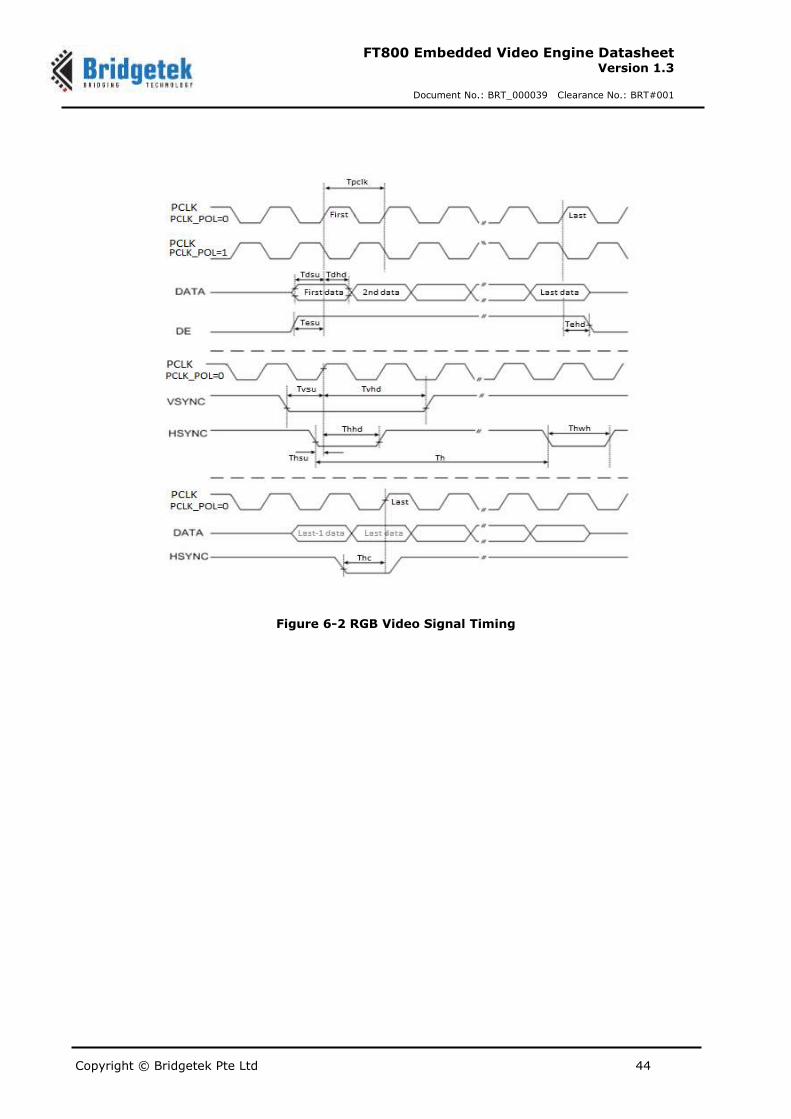
Copyright © Bridgetek Pte Ltd 44
FT800 Embedded Video Engine Datasheet Version 1.3
Document No.: BRT_000039 Clearance No.: BRT#001
Figure 6-2 RGB Video Signal Timing
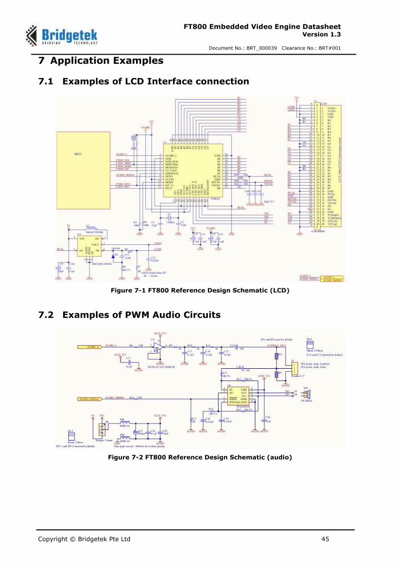
Copyright © Bridgetek Pte Ltd 45
FT800 Embedded Video Engine Datasheet Version 1.3
Document No.: BRT_000039 Clearance No.: BRT#001
7 Application Examples
7.1 Examples of LCD Interface connection
Figure 7-1 FT800 Reference Design Schematic (LCD)
7.2 Examples of PWM Audio Circuits
Figure 7-2 FT800 Reference Design Schematic (audio)
Copyright © Bridgetek Pte Ltd 46
FT800 Embedded Video Engine Datasheet Version 1.3
Document No.: BRT_000039 Clearance No.: BRT#001
8 Package Parameters
The FT800 is available in VQFN-48 package. The solder reflow profile for all packages is described in following sections.
8.1 VQFN-48 Package Dimensions
8.1.1 Top Side
Notes:
1. YYWW = Date Code, where YY is year and WW is week number
2. Pre-date code 1727 company logo was FTDI
3. Marking alignment should be centre justified
4. Laser Marking should be used 5. All marking dimensions should be marked proportionally. Marking font should be using standard
font (Roman Simplex)
8.1.2 Bottom Side
No markings should be placed on the bottom side.
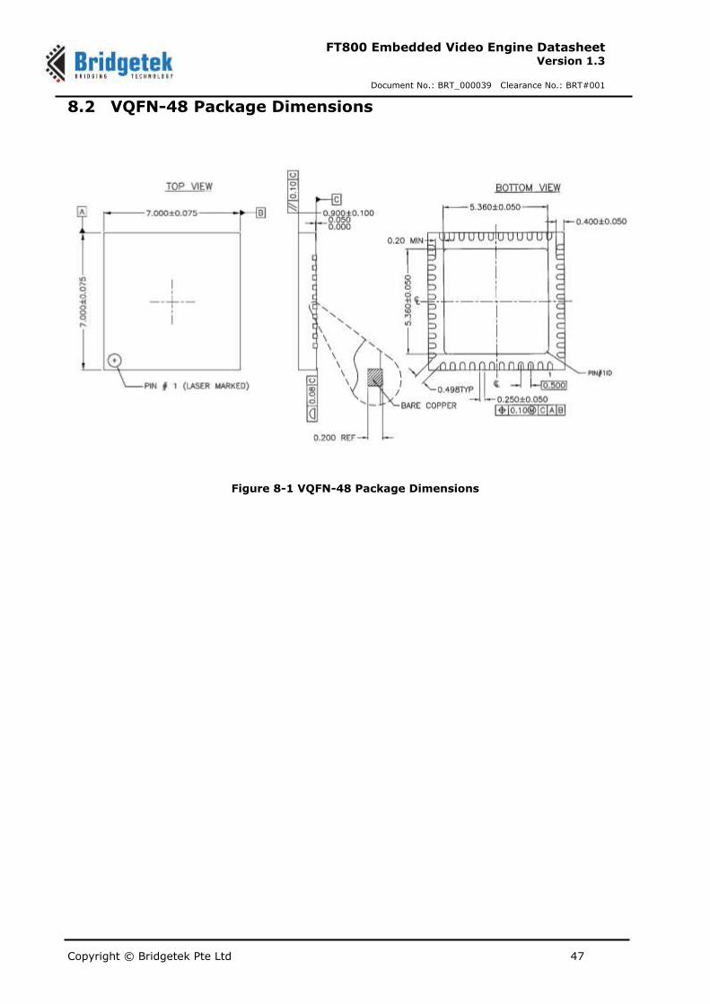
Copyright © Bridgetek Pte Ltd 47
FT800 Embedded Video Engine Datasheet Version 1.3
Document No.: BRT_000039 Clearance No.: BRT#001
8.2 VQFN-48 Package Dimensions
Figure 8-1 VQFN-48 Package Dimensions
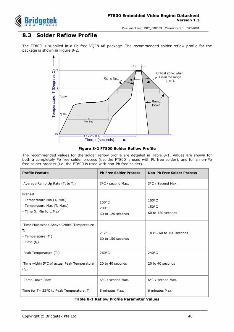
Copyright © Bridgetek Pte Ltd 48
FT800 Embedded Video Engine Datasheet Version 1.3
Document No.: BRT_000039 Clearance No.: BRT#001
8.3 Solder Reflow Profile
The FT800 is supplied in a Pb free VQFN-48 package. The recommended solder reflow profile for the
package is shown in Figure 8-2.
Figure 8-2 FT800 Solder Reflow Profile
The recommended values for the solder reflow profile are detailed in Table 8-1. Values are shown for both a completely Pb free solder process (i.e. the FT800 is used with Pb free solder), and for a non-Pb
free solder process (i.e. the FT800 is used with non-Pb free solder).
Profile Feature Pb Free Solder Process Non-Pb Free Solder Process
Average Ramp Up Rate (Ts to Tp) 3°C / second Max. 3°C / Second Max.
Preheat
- Temperature Min (Ts Min.)
- Temperature Max (Ts Max.)
- Time (ts Min to ts Max)
150°C
200°C
60 to 120 seconds
100°C
150°C
60 to 120 seconds
Time Maintained Above Critical Temperature
TL:
- Temperature (TL)
- Time (tL)
217°C
60 to 150 seconds
183°C 60 to 150 seconds
Peak Temperature (Tp) 260°C 240°C
Time within 5°C of actual Peak Temperature
(tp)
20 to 40 seconds 20 to 40 seconds
Ramp Down Rate 6°C / second Max. 6°C / second Max.
Time for T= 25°C to Peak Temperature, Tp 8 minutes Max. 6 minutes Max.
Table 8-1 Reflow Profile Parameter Values
Critical Zone: when
T is in the range
T to T
Tem
pe
ratu
re,
T (
Deg
rees C
)
Time, t (seconds)
25PT = 25º C to T
tp
Tp
TL
tPreheat
S
tL
Ramp UpL p
Ramp
Down
T MaxS
T MinS
Copyright © Bridgetek Pte Ltd 49
FT800 Embedded Video Engine Datasheet Version 1.3
Document No.: BRT_000039 Clearance No.: BRT#001
9 Contact Information
Head Quarters – Singapore Branch Office – Taipei, Taiwan
Bridgetek Pte Ltd 178 Paya Lebar Road, #07-03 Singapore 409030 Tel: +65 6547 4827 Fax: +65 6841 6071
Bridgetek Pte Ltd, Taiwan Branch 2 Floor, No. 516, Sec. 1, Nei Hu Road, Nei Hu District Taipei 114 Taiwan , R.O.C. Tel: +886 (2) 8797 5691 Fax: +886 (2) 8751 9737
E-mail (Sales) [email protected] E-mail (Sales) [email protected] E-mail (Support) [email protected] E-mail (Support) [email protected]
Branch Office - Glasgow, United Kingdom Branch Office – Vietnam
Bridgetek Pte. Ltd. Unit 1, 2 Seaward Place, Centurion Business Park Glasgow G41 1HH United Kingdom Tel: +44 (0) 141 429 2777 Fax: +44 (0) 141 429 2758
Bridgetek VietNam Company Limited Lutaco Tower Building, 5th Floor, 173A Nguyen Van Troi, Ward 11, Phu Nhuan District, Ho Chi Minh City, Vietnam Tel : 08 38453222 Fax : 08 38455222
E-mail (Sales) [email protected] E-mail (Sales) [email protected] E-mail (Support) [email protected] E-mail (Support) [email protected]
Web Site
http://brtchip.com/
Distributor and Sales Representatives
Please visit the Sales Network page of the Bridgetek Web site for the contact details of our distributor(s) and sales representative(s) in your country.
System and equipment manufacturers and designers are responsible to ensure that their systems, and any Bridgetek Pte Ltd (BRT
Chip) devices incorporated in their systems, meet all applicable safety, regulatory and system-level performance requirements. All
application-related information in this document (including application descriptions, suggested Bridgetek devices and other materials) is
provided for reference only. While Bridgetek has taken care to assure it is accurate, this information is subject to customer
confirmation, and Bridgetek disclaims all liability for system designs and for any applications assistance provided by Bridgetek. Use of
Bridgetek devices in life support and/or safety applications is entirely at the user’s risk, and the user agrees to defend, indemnify and
hold harmless Bridgetek from any and all damages, claims, suits or expense resulting from such use. This document is subject to
change without notice. No freedom to use patents or other intellectual property rights is implied by the publication of this document. Neither the whole nor any part of the information contained in, or the product described in this document, may be adapted or
reproduced in any material or electronic form without the prior written consent of the copyright holder. Bridgetek Pte Ltd, 178 Paya
Lebar Road, #07-03, Singapore 409030. Singapore Registered Company Number: 201542387H.
Copyright © Bridgetek Pte Ltd 50
FT800 Embedded Video Engine Datasheet Version 1.3
Document No.: BRT_000039 Clearance No.: BRT#001
Appendix A – References
Document References
FT800 Series Programmers Guide
AN_240 FT800 From the Ground Up
AN_245 Sample Application Introduction for VM800B & VM800C Development Kits & Windows PC
AN_246 VM800 Series ‘Sample App’
AN_252 FT800 Audio Primer
AN_299 FT800_FT801 Internal Clock Trimming
Acronyms and Abbreviations
Terms Description
ADPCM Adaptive Differential Pulse Code Modulation
ASCII American Standard Code for Information Interchange
EVE Embedded Video Engine
HMI Human Machine Interfaces
I2C Inter-Integrated Circuit
LCD Liquid Crystal Display
LED Light Emitting Diode
MCU Micro Controller Unit
MPU Micro Processor Unit
PCM Pulse Code Modulation
PLL Phased Locked Loop
PWM Pulse Width Modulation
QVGA Quarter Video Graphics Array
ROM Read Only Memory
SPI Serial Peripheral Interface
VQFN Very Thin Quad Flat Non-Leaded Package
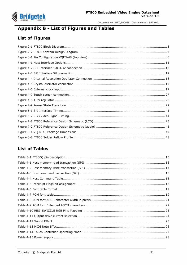
Copyright © Bridgetek Pte Ltd 51
FT800 Embedded Video Engine Datasheet Version 1.3
Document No.: BRT_000039 Clearance No.: BRT#001
Appendix B - List of Figures and Tables
List of Figures
Figure 2-1 FT800 Block Diagram ..................................................................................................... 3
Figure 2-2 FT800 System Design Diagram ....................................................................................... 3
Figure 3-1 Pin Configuration VQFN-48 (top view) .............................................................................. 6
Figure 4-1 Host Interface Options ................................................................................................. 11
Figure 4-2 SPI Interface 1.8-3.3V connection ................................................................................. 12
Figure 4-3 SPI Interface 5V connection .......................................................................................... 12
Figure 4-4 Internal Relaxation Oscillator Connection ....................................................................... 16
Figure 4-5 Crystal oscillator connection ......................................................................................... 17
Figure 4-6 External clock input ..................................................................................................... 17
Figure 4-7 Touch screen connection .............................................................................................. 27
Figure 4-8 1.2V regulator ............................................................................................................ 28
Figure 4-9 Power State Transition ................................................................................................. 29
Figure 6-1 SPI Interface Timing .................................................................................................... 41
Figure 6-2 RGB Video Signal Timing .............................................................................................. 44
Figure 7-1 FT800 Reference Design Schematic (LCD) ...................................................................... 45
Figure 7-2 FT800 Reference Design Schematic (audio) .................................................................... 45
Figure 8-1 VQFN-48 Package Dimensions ...................................................................................... 47
Figure 8-2 FT800 Solder Reflow Profile .......................................................................................... 48
List of Tables
Table 3-1 FT800Q pin description.................................................................................................. 10
Table 4-1 Host memory read transaction (SPI) ............................................................................... 13
Table 4-2 Host memory write transaction (SPI) .............................................................................. 14
Table 4-3 Host command transaction (SPI) .................................................................................... 15
Table 4-4 Host Command Table .................................................................................................... 15
Table 4-5 Interrupt Flags bit assignment ....................................................................................... 16
Table 4-6 Font table format ......................................................................................................... 19
Table 4-7 ROM font table ............................................................................................................. 19
Table 4-8 ROM font ASCII character width in pixels ......................................................................... 21
Table 4-9 ROM font Extended ASCII characters .............................................................................. 22
Table 4-10 REG_SWIZZLE RGB Pins Mapping ................................................................................. 23
Table 4-11 Output drive current selection ...................................................................................... 24
Table 4-12 Sound Effect .............................................................................................................. 25
Table 4-13 MIDI Note Effect ......................................................................................................... 26
Table 4-14 Touch Controller Operating Mode .................................................................................. 27
Table 4-15 Power supply ............................................................................................................. 28
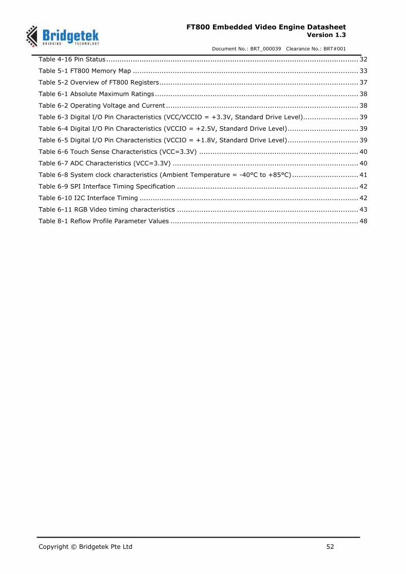
Copyright © Bridgetek Pte Ltd 52
FT800 Embedded Video Engine Datasheet Version 1.3
Document No.: BRT_000039 Clearance No.: BRT#001
Table 4-16 Pin Status .................................................................................................................. 32
Table 5-1 FT800 Memory Map ...................................................................................................... 33
Table 5-2 Overview of FT800 Registers .......................................................................................... 37
Table 6-1 Absolute Maximum Ratings ............................................................................................ 38
Table 6-2 Operating Voltage and Current ....................................................................................... 38
Table 6-3 Digital I/O Pin Characteristics (VCC/VCCIO = +3.3V, Standard Drive Level) ......................... 39
Table 6-4 Digital I/O Pin Characteristics (VCCIO = +2.5V, Standard Drive Level) ................................ 39
Table 6-5 Digital I/O Pin Characteristics (VCCIO = +1.8V, Standard Drive Level) ................................ 39
Table 6-6 Touch Sense Characteristics (VCC=3.3V) ........................................................................ 40
Table 6-7 ADC Characteristics (VCC=3.3V) .................................................................................... 40
Table 6-8 System clock characteristics (Ambient Temperature = -40°C to +85°C) .............................. 41
Table 6-9 SPI Interface Timing Specification .................................................................................. 42
Table 6-10 I2C Interface Timing ................................................................................................... 42
Table 6-11 RGB Video timing characteristics .................................................................................. 43
Table 8-1 Reflow Profile Parameter Values ..................................................................................... 48
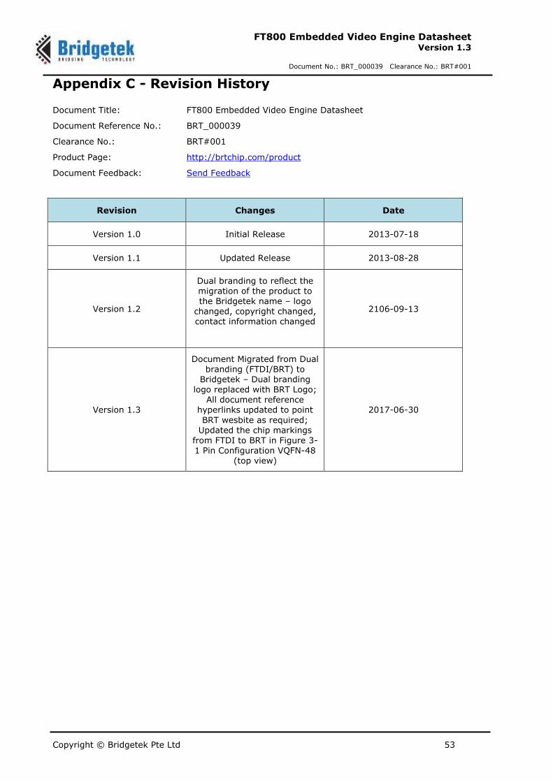
Copyright © Bridgetek Pte Ltd 53
FT800 Embedded Video Engine Datasheet Version 1.3
Document No.: BRT_000039 Clearance No.: BRT#001
Appendix C - Revision History
Document Title: FT800 Embedded Video Engine Datasheet
Document Reference No.: BRT_000039
Clearance No.: BRT#001
Product Page: http://brtchip.com/product
Document Feedback: Send Feedback
Revision Changes Date
Version 1.0 Initial Release 2013-07-18
Version 1.1 Updated Release 2013-08-28
Version 1.2
Dual branding to reflect the migration of the product to the Bridgetek name – logo
changed, copyright changed, contact information changed
2106-09-13
Version 1.3
Document Migrated from Dual branding (FTDI/BRT) to
Bridgetek – Dual branding logo replaced with BRT Logo;
All document reference hyperlinks updated to point
BRT wesbite as required; Updated the chip markings
from FTDI to BRT in Figure 3-1 Pin Configuration VQFN-48
(top view)
2017-06-30