an_240 ft800 from the ground up - ftdi
TRANSCRIPT
Use of FTDI devices in life support and/or safety applications is entirely at the user’s risk, and the user agrees to defend, indemnify and hold FTDI harmless from any and all damages, claims, suits
or expense resulting from such use.
Future Technology Devices International Limited (FTDI) Unit 1, 2 Seaward Place, Glasgow G41 1HH, United Kingdom Tel.: +44 (0) 141 429 2777 Fax: + 44 (0) 141 429 2758
Web Site: http://ftdichip.com Copyright © 2014 Future Technology Devices International Limited
Application Note
AN_240
FT800 From the Ground Up
Version 1.1
Issue Date: 2014-06-09
The FTDI FT800 video controller offers a low cost solution for embedded graphics requirements. In addition to the graphics, resistive touch inputs and an audio output provide a complete human machine interface to the outside
world.
This application note will describe the process of integrating the FT800 into a design with a simple MCU.
Application Note
AN_240 FT800 From the Ground Up Version 1.1 Document Reference No.: FT_000827 Clearance No.: FTDI# 346
1
Copyright © 2014 Future Technology Devices International Limited
Table of Contents
1 Introduction .................................................................................................................................... 3
2 Hardware ........................................................................................................................................ 4
2.1 MCU Selection ......................................................................................................................... 4
2.2 Display Selection ..................................................................................................................... 4
2.3 Display Connection to FT800 .................................................................................................. 5
2.3.1 Display orientation .......................................................................................................... 5
2.3.2 Color Data ....................................................................................................................... 5
2.3.3 Display Timing ................................................................................................................. 5
2.3.4 Display Enable ................................................................................................................. 7
2.3.5 Backlight .......................................................................................................................... 7
2.4 Touch Panel Integration .......................................................................................................... 7
2.4.1 Resistive touch panel ...................................................................................................... 7
2.4.2 Capacitive touch panel .................................................................................................... 7
2.5 Audio Integration .................................................................................................................... 8
2.6 MCU connection ..................................................................................................................... 8
2.6.1 SPI slave ........................................................................................................................... 8
2.6.2 I2C slave ........................................................................................................................... 8
2.6.3 Clock, GPIO, Power & Control ......................................................................................... 8
2.7 Example circuit ........................................................................................................................ 9
3 Data Transfers ............................................................................................................................... 10
3.1 Host Memory Read ............................................................................................................... 10
3.2 Host Memory Write .............................................................................................................. 11
3.3 Host Command Write ........................................................................................................... 12
4 Software ........................................................................................................................................ 14
4.1 Memory Map ........................................................................................................................ 14
4.2 Configuration ........................................................................................................................ 15
4.2.1 MCU setup .................................................................................................................... 15
4.2.2 Wake Up ........................................................................................................................ 15
4.2.3 Configure the Display Timing ........................................................................................ 15
Application Note
AN_240 FT800 From the Ground Up Version 1.1 Document Reference No.: FT_000827 Clearance No.: FTDI# 346
2
Copyright © 2014 Future Technology Devices International Limited
4.2.4 Configure the Touch Sensitivity .................................................................................... 16
4.2.5 Configure the audio ...................................................................................................... 17
4.2.6 Initialize and enable the display .................................................................................... 17
4.3 Application ............................................................................................................................ 19
4.3.1 Create Display Lists ....................................................................................................... 19
4.3.2 Update the Display List ................................................................................................. 20
4.3.3 Widgets & the FT800 Graphics Engine .......................................................................... 20
5 FT800 Design Summary ................................................................................................................. 23
6 Collateral Support from FTDI ........................................................................................................ 25
7 Contact Information ...................................................................................................................... 26
Appendix A – References ...................................................................................................................... 27
Document References ....................................................................................................................... 27
Acronyms and Abbreviations ............................................................................................................ 27
Appendix B – List of Tables & Figures ................................................................................................... 28
List of Tables ..................................................................................................................................... 28
List of Figures .................................................................................................................................... 28
Appendix C – Revision History .............................................................................................................. 29
Application Note
AN_240 FT800 From the Ground Up Version 1.1 Document Reference No.: FT_000827 Clearance No.: FTDI# 346
3
Copyright © 2014 Future Technology Devices International Limited
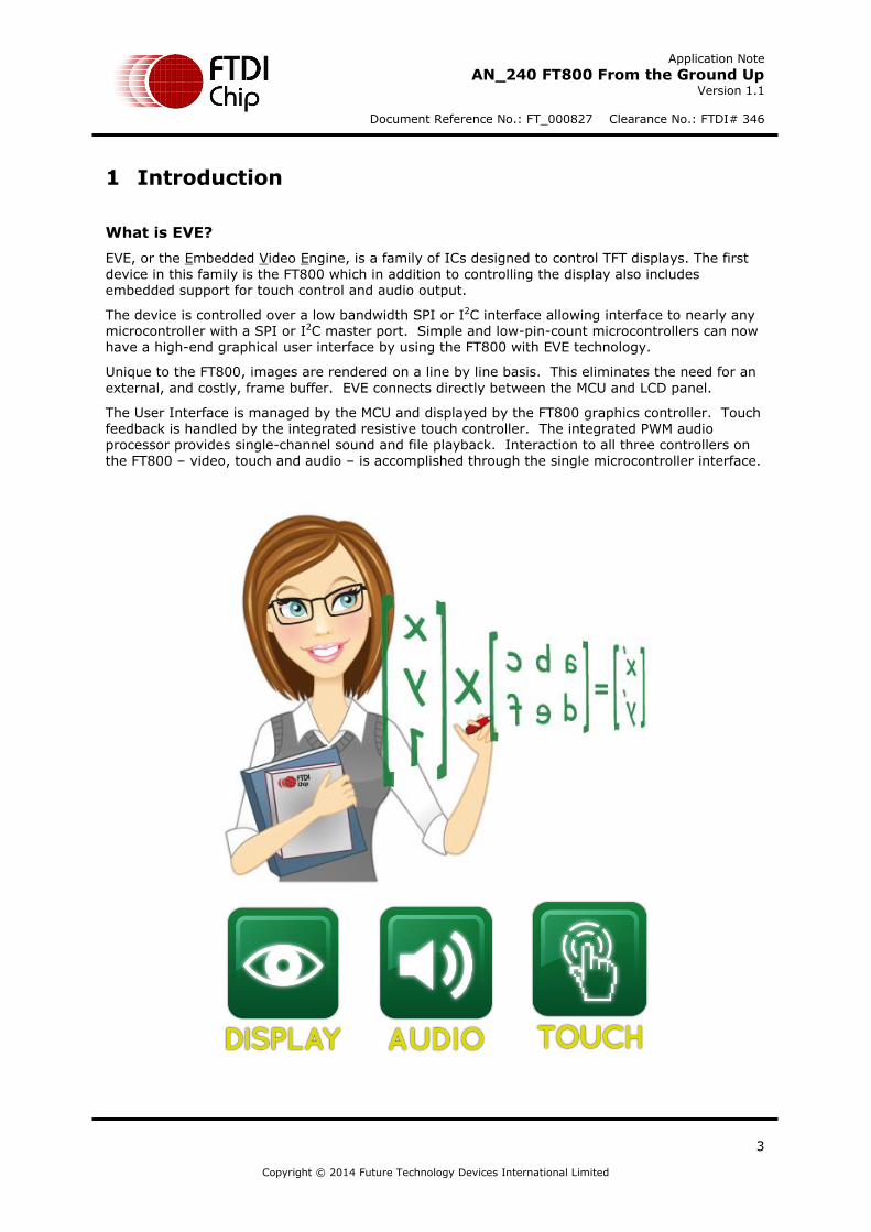
1 Introduction
What is EVE?
EVE, or the Embedded Video Engine, is a family of ICs designed to control TFT displays. The first
device in this family is the FT800 which in addition to controlling the display also includes embedded support for touch control and audio output.
The device is controlled over a low bandwidth SPI or I2C interface allowing interface to nearly any microcontroller with a SPI or I2C master port. Simple and low-pin-count microcontrollers can now have a high-end graphical user interface by using the FT800 with EVE technology.
Unique to the FT800, images are rendered on a line by line basis. This eliminates the need for an
external, and costly, frame buffer. EVE connects directly between the MCU and LCD panel.
The User Interface is managed by the MCU and displayed by the FT800 graphics controller. Touch feedback is handled by the integrated resistive touch controller. The integrated PWM audio processor provides single-channel sound and file playback. Interaction to all three controllers on the FT800 – video, touch and audio – is accomplished through the single microcontroller interface.
Application Note
AN_240 FT800 From the Ground Up Version 1.1 Document Reference No.: FT_000827 Clearance No.: FTDI# 346
4
Copyright © 2014 Future Technology Devices International Limited
2 Hardware
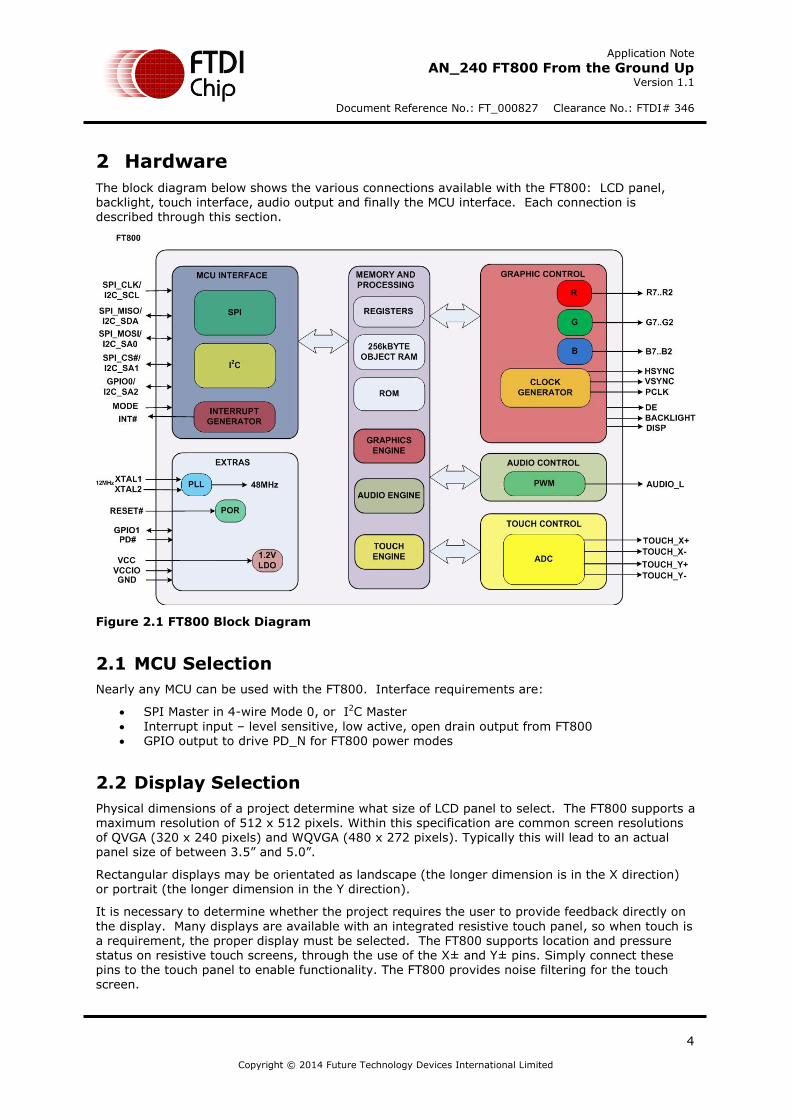
The block diagram below shows the various connections available with the FT800: LCD panel, backlight, touch interface, audio output and finally the MCU interface. Each connection is described through this section.
Figure 2.1 FT800 Block Diagram
2.1 MCU Selection
Nearly any MCU can be used with the FT800. Interface requirements are:
SPI Master in 4-wire Mode 0, or I2C Master
Interrupt input – level sensitive, low active, open drain output from FT800 GPIO output to drive PD_N for FT800 power modes
2.2 Display Selection
Physical dimensions of a project determine what size of LCD panel to select. The FT800 supports a maximum resolution of 512 x 512 pixels. Within this specification are common screen resolutions of QVGA (320 x 240 pixels) and WQVGA (480 x 272 pixels). Typically this will lead to an actual panel size of between 3.5” and 5.0”.
Rectangular displays may be orientated as landscape (the longer dimension is in the X direction) or portrait (the longer dimension in the Y direction).
It is necessary to determine whether the project requires the user to provide feedback directly on
the display. Many displays are available with an integrated resistive touch panel, so when touch is a requirement, the proper display must be selected. The FT800 supports location and pressure status on resistive touch screens, through the use of the X± and Y± pins. Simply connect these pins to the touch panel to enable functionality. The FT800 provides noise filtering for the touch screen.
Application Note
AN_240 FT800 From the Ground Up Version 1.1 Document Reference No.: FT_000827 Clearance No.: FTDI# 346
5
Copyright © 2014 Future Technology Devices International Limited
2.3 Display Connection to FT800
The FT800 will connect directly to the screen without the need for buffering.
2.3.1 Display orientation
Nearly all LCD displays are orientated such that (X, Y) coordinate (0, 0) is located in the upper left corner. All (X, Y) coordinates are positive numbers. X increases as the location is moved from
left-to-right; Y increases as the location moves from top-to-bottom.
Touch panels follow the same coordinate system with (0, 0) in the upper left, although the accuracy may be higher than one pixel allowing for sub-pixel detection.
For the FT800, the anti-aliasing feature is always enabled. Pixels can be defined by the application as a number of sub-pixels, usually in 1/16th pixel increments. While the physical dimensions of a pixel cannot be altered, the color values are sent in such a way to smooth out the
visual appearance of the various items.
2.3.2 Color Data
The colors Red (R), Green (G) and Blue (B) are provided as parallel data to the display. There are 6 bits for each color. If the display supports more bits (sometimes up to 8) simply connect the FT800 data pins to the higher data bits for each color of the display. Refer to the display datasheet whether the unused pins should be left open or pulled to a particular value.
The FT800 supports a re-ordering, or “swizzling”, of the data LCD RGB data bits pin assignments. This allows a direct PCB layout from the FT800 to the LCD connector, with the ability to positively impact electromagnetic (EMI) effects. Refer to the FT800 Datasheet for details surrounding the different connection orders.
2.3.3 Display Timing
Several signals are used to coordinate all of the data and timing required by the display:
PCLK – Pixel Clock – the master clock to latch the signals into the display VSYNC – Vertical Sync – defines the beginning of a frame HSYNC – Horizontal Sync – defines the beginning of a line DE – Data Enable – defines when RGB data is being driven DISP – Display Enable – defines when the overall display is internally powered
The Pixel Clock is used to latch each pixel value and other timing signals into the display. The
FT800 can drive the panel data either on rising or falling edge clocks. Display timing is typically controlled through the Pixel Clock coupled with the Vertical Sync (VSYNC) and Horizontal Sync (HSYNC) pulses.
Although the physical, or “active” size of the display may be a given pixel size (e.g. 480 x 272), the actual number of clocks required to display the full image is not simply (Horizontal * Vertical). An image is comprised of multiple horizontal lines. Each line requires several clocks before and after the active region. In a similar fashion, the total number of lines is greater than the vertical
active region with several lines above and below the active region.
A typical display datasheet will define the pixel clock frequency (REG_PCLK) and whether data is clocked on rising or falling edges (REG_PCLK_POL). It will then describe the horizontal
synchronization pulse start (REG_HSYNC0) and stop (REG_HSYNC1) times as a number of clocks. Vertical synchronization pulse start (REG_VSYNC0) and stop (REG_VSYNC1) are defined as a number of lines.
Sometimes the total number of clocks per line (REG_HCYCLE) and lines per screen (REG_VCYCLE)
are directly shown. Other times, there may be references to “front porch” and “back porch” timing. Add the front and back porch values to the active screen size in a particular direction to obtain the total number of clocks/line or lines/screen.
Application Note
AN_240 FT800 From the Ground Up Version 1.1 Document Reference No.: FT_000827 Clearance No.: FTDI# 346
6
Copyright © 2014 Future Technology Devices International Limited
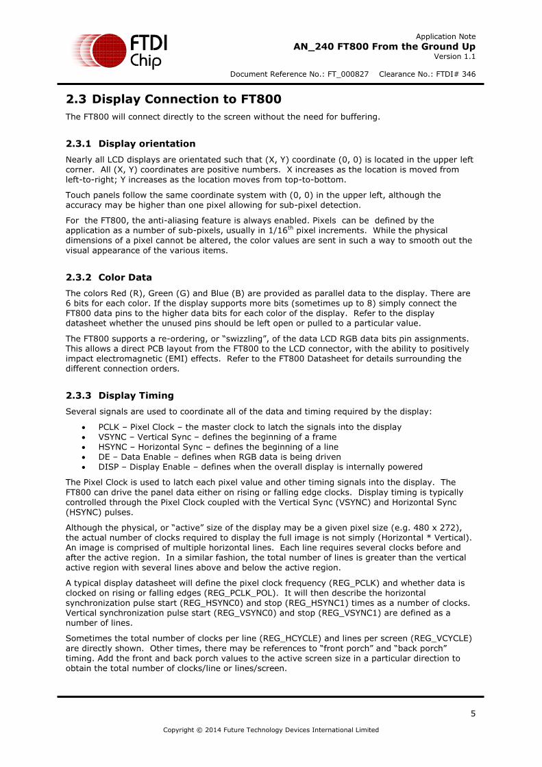
Finally, the offsets need to be defined. These values define exactly where in the screen the active region will be displayed. They are defined as a number of clocks from the start of the HSYNC
signal (REG_HOFFSET) and the number of lines from the start of the VSYNC signal (REG_VOFFSET). During the output of each horizontal line, the Data Enable signal (DE) will be active while data is being output on the RGB signals.
Some displays do not require physical HSYNC or VSYNC signals. Instead, they use the Data Enable (DE) signal which is also provided by the FT800. If DE is used, correct timing calculations and settings for VSYNC and HSYNC still apply even though they may not be connected to the display. Refer to the display datasheet for timing and connection requirements.
The image below correlates the FT800 registers to the timing of a LCD panel. See Section 4.2.3 below for programming the registers and display initialization sequence.
Active Display Region
PCLK
HSYNC
DE
R[7..2], G[7..2], B[7..2]
VSYN
C
REG_HSIZE
REG_HCYCLE (#CLOCKS / LINE)
REG
_VSYN
C0
REG
_VSYN
C1
REG
_VCYCLE (#
LIN
ES/S
CREEN
)
REG_HOFFSET
REG
_VO
FFSET
REG_HSYNC1
REG_HSYNC0
REG
_VSIZ
E
RGB Pixel Data
Figure 2.2 FT800 LCD Timing Registers – Display View
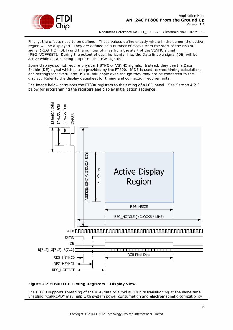
The FT800 supports spreading of the RGB data to avoid all 18 bits transitioning at the same time. Enabling “CSPREAD” may help with system power consumption and electromagnetic compatibility
Application Note
AN_240 FT800 From the Ground Up Version 1.1 Document Reference No.: FT_000827 Clearance No.: FTDI# 346
7
Copyright © 2014 Future Technology Devices International Limited
(EMC) tests since fewer signals are changing simultaneously. The figures below shows the LCD data timing CSPREAD disabled then enabled.
Figure 2.3 LCD RGB timing with CSPREAD disabled
Figure 2.4 LCD RGB timing with CSPREAD enabled
CSPREAD is available with either polarity setting for PCLK.
2.3.4 Display Enable
Displays may have a signal for power control, commonly called Display Enable (DISP). The FT800 provides the DISP signal as a GPIO output that the MCU application can set to logic 1 or logic 0
when required.
2.3.5 Backlight
TFT displays also have a LED backlight that typically requires between 24V and 30V. An external LED driver suitable to generate this voltage is necessary. The FT800 provides a PWM output to adjust the brightness of the display’s LED array.
2.4 Touch Panel Integration
Incorporating a touch panel into an embedded design allows the elimination of a keyboard or other buttons for user feedback. The FT800 can supply the direct touch data, or be coupled with one of the special widgets that track position automatically.
2.4.1 Resistive touch panel
Resistive panels have been available for some time and are robust solutions for many situations including industrial environments. There are no restrictions on whether the user is wearing gloves.
A touch interface is simple – one pair each of X and Y signals. These are connected directly to the FT800.
2.4.2 Capacitive touch panel
Capacitive touch panels are commonly found on tablets, phones and other similar hand-held devices. The user must use their bare finger or use a specially designed glove or stylus. A more
Application Note
AN_240 FT800 From the Ground Up Version 1.1 Document Reference No.: FT_000827 Clearance No.: FTDI# 346
8
Copyright © 2014 Future Technology Devices International Limited
capable MCU may also be required to process the multiple touch points. The FT800 does not support capacitive touch panels.
2.5 Audio Integration
Audio output is also provided by the FT800. As with the PWM backlight output, audio is also supplied as a PWM signal. Filtering and amplification are required to convert the PWM pulses into
an analog waveform suitable to drive a speaker or headphones.
The FT800 can synthesize 60 different MIDI sounds, most with pitch control. Audio file playback is also possible with files formatted as 8-bits signed PCM, 8-bits µLAW or 4-bits IMA-ADPCM.
2.6 MCU connection
The last piece of the puzzle is the connection to the host MCU. The MCU needs to provide a SPI
master or an I2C master interface as noted below.
2.6.1 SPI slave
30Mbps maximum rate Unmanaged
Mode 0 Most significant bit (MSB) first
The SPI MCU interface consists of the following signals:
SPI_SCK – SPI clock SPI_MOSI – Master Out / Slave In – data from the MCU to the FT800 SPI_MISO – Master In / Slave Out – data from the FT800 to the MCU SPI_SS_N – SPI Slave Select, low active
INT_N – Interrupt output from FT800 PD_N – Power down input to the FT800 Two GPIO signals are available to be used as necessary
MODE – FT800 input – pull down to select SPI
2.6.2 I2C slave
3.4Mbps maximum rate Configurable device address (0x20 through 0x27)
The I2C MCU interface consists of the following signals:
I2C_SCL – I2C clock I2C_SDA – I2C data I2C_A2, I2C_A1, I2C_A0 – I2C Slave Address (add 0x20 for the full address)
o Binary address = (MSB) 0, 1, 0, I2C_A2, I2C_A1, I2C_A0 (LSB)
INT_N – Interrupt output from FT800 PD_N – Power down input to the FT800 One GPIO signal is available to be used as necessary MODE – FT800 input – pull up to select I2C
2.6.3 Clock, GPIO, Power & Control
The FT800 uses an external 12MHz crystal or logic-level oscillator.
Two GPIO signals are required for interrupt and power control.
The FT800 requires two power supplies: VCC and VCCIO. VCC provides the reference for the LCD interface and is fixed at 3.3V. VCCIO provides the reference for the MCU interface with an allowable range of 1.8V to 3.3V. An internal regulator supplies 1.2V for the FT800 core.
Application Note
AN_240 FT800 From the Ground Up Version 1.1 Document Reference No.: FT_000827 Clearance No.: FTDI# 346
9
Copyright © 2014 Future Technology Devices International Limited
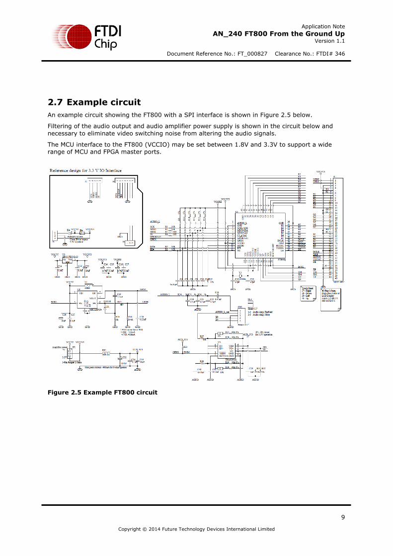
2.7 Example circuit
An example circuit showing the FT800 with a SPI interface is shown in Figure 2.5 below.
Filtering of the audio output and audio amplifier power supply is shown in the circuit below and
necessary to eliminate video switching noise from altering the audio signals.
The MCU interface to the FT800 (VCCIO) may be set between 1.8V and 3.3V to support a wide range of MCU and FPGA master ports.
Figure 2.5 Example FT800 circuit
Application Note
AN_240 FT800 From the Ground Up Version 1.1 Document Reference No.: FT_000827 Clearance No.: FTDI# 346
10
Copyright © 2014 Future Technology Devices International Limited
3 Data Transfers
The FT800 supports a common data communication scheme, regardless of whether the SPI or I2C interface is selected.
The FT800 utilizes a 4MB address space for graphic, touch and audio controller registers as well as memory buffers for use with each controller. The memory map is defined in Section 5 of the FT800 Datasheet.
The host reads and writes the FT800 address space using SPI or I²C transactions. These
transactions are defined as Memory Read, Memory Write, and Command Write as described in the following sections.
Both interfaces use the same byte ordering. Multiple bytes are sent as “Little Endian”. For example, the REG_FREQUENCY register has a default value of 0x02DC6C00 after reset. When reading this value, the byte order on the MCU interface is: 0x00, 0x6Ch, 0xDC, 0x02.
SPI data is sent by the most significant bit first, mode zero.
I²C transactions are encapsulated in the I²C protocol.
For SPI operation, each transaction starts with SS_N goes low, and ends when SS_N goes high. There’s no limit on data length within one transaction, as long as the memory addresses are continuous.
Access to the address space is done over three interface commands:
Host Memory Read Host Memory Write
Host Command Write
There is no command read.
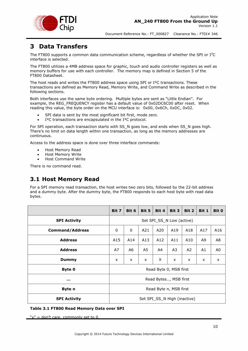
3.1 Host Memory Read
For a SPI memory read transaction, the host writes two zero bits, followed by the 22-bit address and a dummy byte. After the dummy byte, the FT800 responds to each host byte with read data
bytes.
Bit 7 Bit 6 Bit 5 Bit 4 Bit 3 Bit 2 Bit 1 Bit 0
SPI Activity Set SPI_SS_N Low (active)
Command/Address 0 0 A21 A20 A19 A18 A17 A16
Address A15 A14 A13 A12 A11 A10 A9 A8
Address A7 A6 A5 A4 A3 A2 A1 A0
Dummy x x x X x x x x
Byte 0 Read Byte 0, MSB first
… Read Bytes…, MSB first
Byte n Read Byte n, MSB first
SPI Activity Set SPI_SS_N High (inactive)
Table 3.1 FT800 Read Memory Data over SPI
“x” = don’t care, commonly set to 0.
Application Note
AN_240 FT800 From the Ground Up Version 1.1 Document Reference No.: FT_000827 Clearance No.: FTDI# 346
11
Copyright © 2014 Future Technology Devices International Limited
During the time data is being read from the FT800 on the MISO signal, activity on the MOSI signal is ignored.
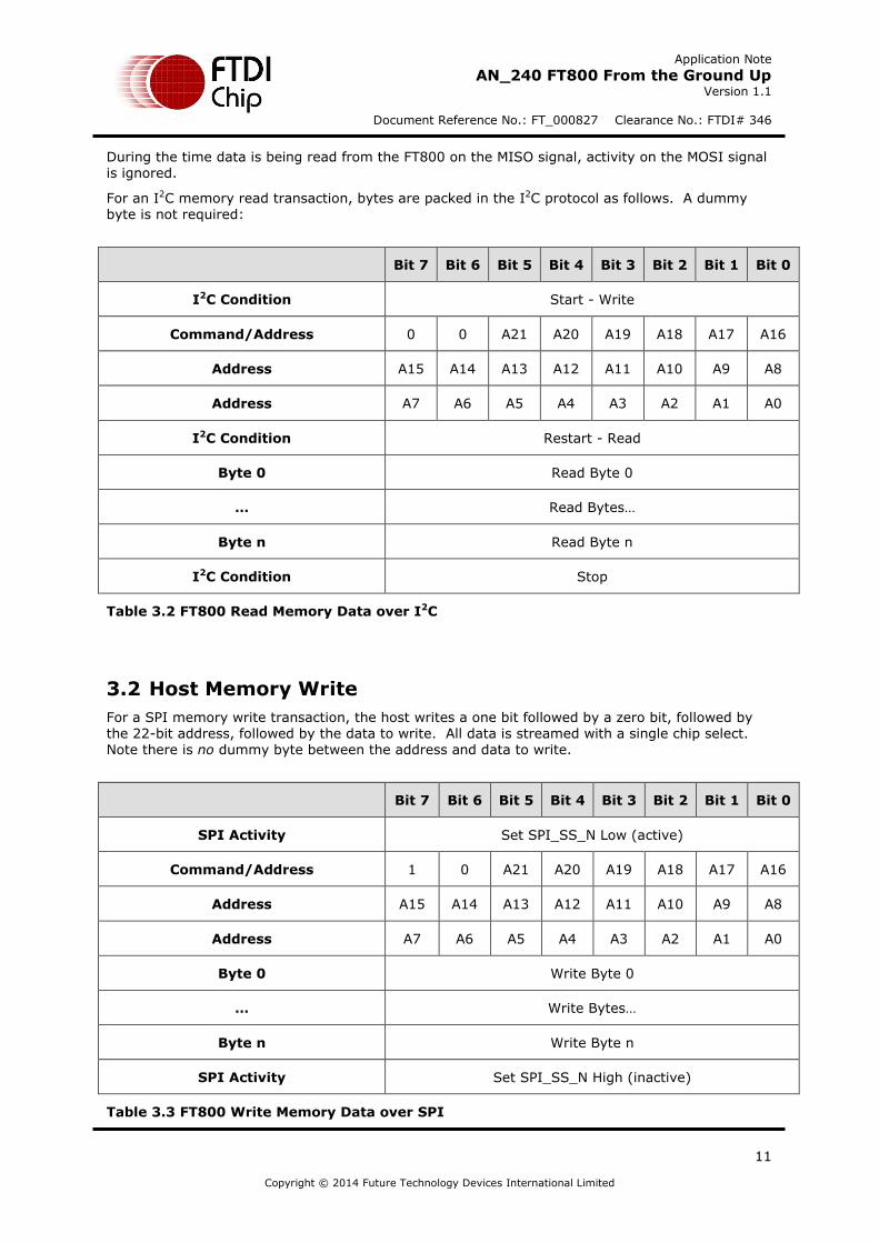
For an I2C memory read transaction, bytes are packed in the I2C protocol as follows. A dummy byte is not required:
Bit 7 Bit 6 Bit 5 Bit 4 Bit 3 Bit 2 Bit 1 Bit 0
I2C Condition Start - Write
Command/Address 0 0 A21 A20 A19 A18 A17 A16
Address A15 A14 A13 A12 A11 A10 A9 A8
Address A7 A6 A5 A4 A3 A2 A1 A0
I2C Condition Restart - Read
Byte 0 Read Byte 0
… Read Bytes…
Byte n Read Byte n
I2C Condition Stop
Table 3.2 FT800 Read Memory Data over I2C
3.2 Host Memory Write
For a SPI memory write transaction, the host writes a one bit followed by a zero bit, followed by the 22-bit address, followed by the data to write. All data is streamed with a single chip select. Note there is no dummy byte between the address and data to write.
Bit 7 Bit 6 Bit 5 Bit 4 Bit 3 Bit 2 Bit 1 Bit 0
SPI Activity Set SPI_SS_N Low (active)
Command/Address 1 0 A21 A20 A19 A18 A17 A16
Address A15 A14 A13 A12 A11 A10 A9 A8
Address A7 A6 A5 A4 A3 A2 A1 A0
Byte 0 Write Byte 0
… Write Bytes…
Byte n Write Byte n
SPI Activity Set SPI_SS_N High (inactive)
Table 3.3 FT800 Write Memory Data over SPI
Application Note
AN_240 FT800 From the Ground Up Version 1.1 Document Reference No.: FT_000827 Clearance No.: FTDI# 346
12
Copyright © 2014 Future Technology Devices International Limited
During the time data is being written to the FT800 on the MOSI signal, activity on the MISO signal is ignored.
For an I2C memory write transaction, bytes are packed in the I2C protocol as follows:
Bit 7 Bit 6 Bit 5 Bit 4 Bit 3 Bit 2 Bit 1 Bit 0
I2C Condition Start - Write
Command/Address 1 0 A21 A20 A19 A18 A17 A16
Address A15 A14 A13 A12 A11 A10 A9 A8
Address A7 A6 A5 A4 A3 A2 A1 A0
Byte 0 Write Byte 0
… Write Bytes…
Byte n Write Byte n
I2C Condition Stop
Table 3.4 FT800 Write Memory Data over I2C
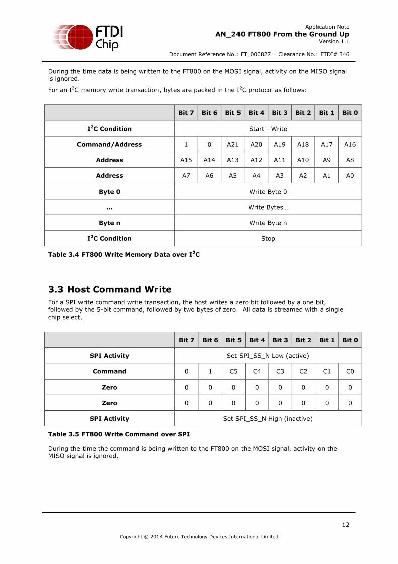
3.3 Host Command Write
For a SPI write command write transaction, the host writes a zero bit followed by a one bit, followed by the 5-bit command, followed by two bytes of zero. All data is streamed with a single
chip select.
Bit 7 Bit 6 Bit 5 Bit 4 Bit 3 Bit 2 Bit 1 Bit 0
SPI Activity Set SPI_SS_N Low (active)
Command 0 1 C5 C4 C3 C2 C1 C0
Zero 0 0 0 0 0 0 0 0
Zero 0 0 0 0 0 0 0 0
SPI Activity Set SPI_SS_N High (inactive)
Table 3.5 FT800 Write Command over SPI
During the time the command is being written to the FT800 on the MOSI signal, activity on the MISO signal is ignored.
Application Note
AN_240 FT800 From the Ground Up Version 1.1 Document Reference No.: FT_000827 Clearance No.: FTDI# 346
13
Copyright © 2014 Future Technology Devices International Limited
For an I2C memory write transaction, bytes are packed in the I2C protocol as follows:
Bit 7 Bit 6 Bit 5 Bit 4 Bit 3 Bit 2 Bit 1 Bit 0
I2C condition Start - Write
Command 0 1 C5 C4 C3 C2 C1 C0
Zero 0 0 0 0 0 0 0 0
Zero 0 0 0 0 0 0 0 0
I2C Condition Stop
Table 3.6 FT800 Write Command over I2C
NOTE: Issuing the ACTIVE command wakes the FT800 from sleep or standby. The ACTIVE command is accomplished by writing three bytes of 00h to address zero.
There are only six commands, so it may be desirable to create individual calls in firmware for each one:
Command Value (including
bits 6 & 7) Description
Power Modes
ACTIVE 0x00 Switch from Standby/Sleep modes to active mode. Write three bytes of 00h to issue the ACTIVE command
STANDBY 0x41 Put FT800 core to standby mode. Clock gate off, PLL and Oscillator remain on (default).
SLEEP 0x42 Put FT800 core to sleep mode. Clock gate off, PLL and Oscillator off.
PWRDOWN 0x50 Switch off 1.2V internal regulator. Clock, PLL and Oscillator off.
Clock Switching
CLKEXT 0x44 Enable PLL input from Crystal oscillator or external input clock.
CLK48M 0x62 Switch PLL output clock to 48MHz (default).
CLK36M 0x61 Switch PLL output clock to 36MHz.
Miscellaneous
CORERST 0x68 Send reset pulse to FT800 core. All registers and state
machines will be reset.
Table 3.7 FT800 Commands
Application Note
AN_240 FT800 From the Ground Up Version 1.1 Document Reference No.: FT_000827 Clearance No.: FTDI# 346
14
Copyright © 2014 Future Technology Devices International Limited
4 Software
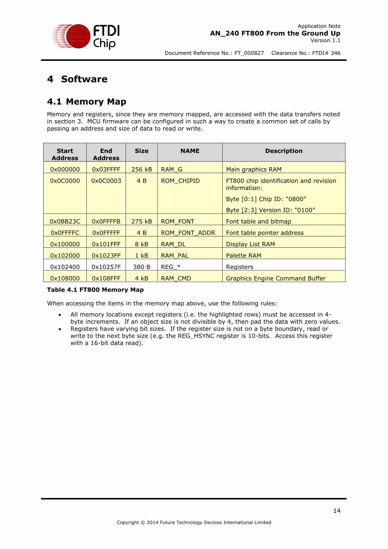
4.1 Memory Map
Memory and registers, since they are memory mapped, are accessed with the data transfers noted in section 3. MCU firmware can be configured in such a way to create a common set of calls by passing an address and size of data to read or write.
Start
Address
End
Address
Size NAME Description
0x000000 0x03FFFF 256 kB RAM_G Main graphics RAM
0x0C0000 0x0C0003 4 B ROM_CHIPID FT800 chip identification and revision
information:
Byte [0:1] Chip ID: “0800”
Byte [2:3] Version ID: “0100”
0x0BB23C 0x0FFFFB 275 kB ROM_FONT Font table and bitmap
0x0FFFFC 0x0FFFFF 4 B ROM_FONT_ADDR Font table pointer address
0x100000 0x101FFF 8 kB RAM_DL Display List RAM
0x102000 0x1023FF 1 kB RAM_PAL Palette RAM
0x102400 0x10257F 380 B REG_* Registers
0x108000 0x108FFF 4 kB RAM_CMD Graphics Engine Command Buffer
Table 4.1 FT800 Memory Map
When accessing the items in the memory map above, use the following rules:
All memory locations except registers (i.e. the highlighted rows) must be accessed in 4-byte increments. If an object size is not divisible by 4, then pad the data with zero values.
Registers have varying bit sizes. If the register size is not on a byte boundary, read or write to the next byte size (e.g. the REG_HSYNC register is 10-bits. Access this register with a 16-bit data read).
Application Note
AN_240 FT800 From the Ground Up Version 1.1 Document Reference No.: FT_000827 Clearance No.: FTDI# 346
15
Copyright © 2014 Future Technology Devices International Limited
4.2 Configuration
4.2.1 MCU setup
4.2.1.1 SPI
<=10MHz initial SPI clock o Use slower clock while on internal oscillator
Mode zero o CPOL = 0 – clock idles at zero o CPHA = 0 – data is sampled on rising edge, propagated on falling edge
Little Endian data byte ordering
4.2.1.2 I2C
I2C address of 0x20 through 0x27, depending on the I2C_A2, I2C_A1 and I2C_A0 pins of
the FT800 Maximum rate = 3.4Mbps
Little Endian data byte ordering
Since the data ordering is the same regardless whether SPI or I2C is in use, the remainder of the document will simply call the MCU-FT800 connection as “the interface”.
4.2.2 Wake Up
After configuring the MCU interface the first step in communicating with the FT800 is to wake it up.
1) Reset the FT800
Drive PD_N low for 20ms, then back high Wait for 20ms after PD_N is high
2) Issue the Wake-up command Write 0x00, 0x00, 0x00
3) If using an external crystal or clock source on the FT800, issue the external clock command
Write 0x44, 0x00, 0x00
4) Set the FT800 internal clock speed to 48MHz Write 0x62, 0x00, 0x00
5) At this point, the Host MCU SPI Master can change the SPI clock up to 30MHz 6) Read the Device ID register
Read one byte from location 0x102400 Check for the value 0x7C
7) Set bit 7 of REG_GPIO to 0 to turn off the LCD DISP signal
Write 0x80 to location 0x102490
4.2.3 Configure the Display Timing
Once the FT800 is awake and the internal clock set and Device ID checked, the next task is to configure the LCD display parameters for the chosen display with the values determined in Section 2.3.3 above.
Note: From this point on, individual Write or Read values will not be shown. For example if
the activity is “Set REG_PCLK to zero”, this implies a Host Memory Write to location 10246Ch with a data value of 00h. Register addresses are found in the FT800 datasheet.
1) Set REG_PCLK to zero - This disables the pixel clock output while the LCD and other
system parameters are configured 2) Set the following registers with values for the chosen display. Typical WQVGA and QVGA
values are shown:
Application Note
AN_240 FT800 From the Ground Up Version 1.1 Document Reference No.: FT_000827 Clearance No.: FTDI# 346
16
Copyright © 2014 Future Technology Devices International Limited
Register Description WQVGA
480 x 272
QVGA
320 x 240
REG_PCLK_POL Pixel Clock Polarity 1 0
REG_HSIZE Image width in pixels 480 320
REG_HCYCLE Total number of clocks per line 548 408
REG_HOFFSET Horizontal image start (pixels from left) 43 70
REG_HSYNC0 Start of HSYNC pulse (falling edge) 0 0
REG_HSYNC1 End of HSYNC pulse (rising edge) 41 10
REG_VSIZE Image height in pixels 272 240
REG_VCYCLE Total number of lines per screen 292 263
REG_VOFFSET Vertical image start (lines from top) 12 13
REG_VSYNC0 Start of VSYNC pulse (falling edge) 0 0
REG_VSYNC1 End of VSYNC pulse (rising edge) 10 2
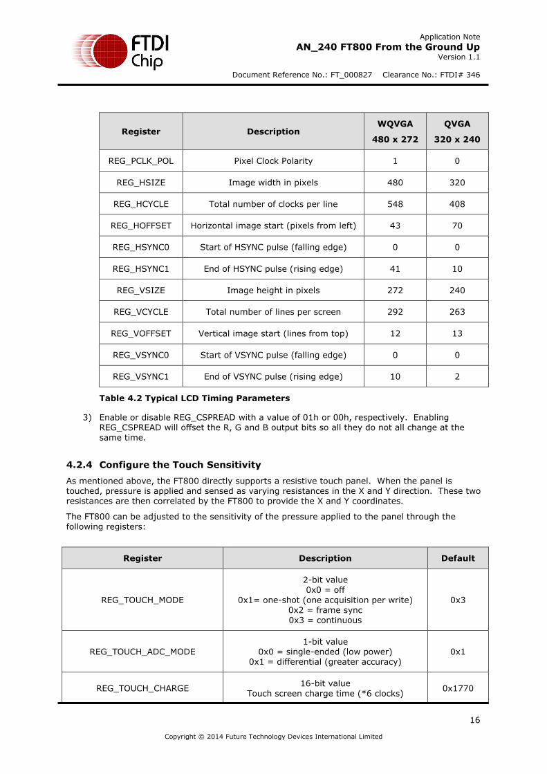
Table 4.2 Typical LCD Timing Parameters
3) Enable or disable REG_CSPREAD with a value of 01h or 00h, respectively. Enabling REG_CSPREAD will offset the R, G and B output bits so all they do not all change at the
same time.
4.2.4 Configure the Touch Sensitivity
As mentioned above, the FT800 directly supports a resistive touch panel. When the panel is touched, pressure is applied and sensed as varying resistances in the X and Y direction. These two resistances are then correlated by the FT800 to provide the X and Y coordinates.
The FT800 can be adjusted to the sensitivity of the pressure applied to the panel through the following registers:
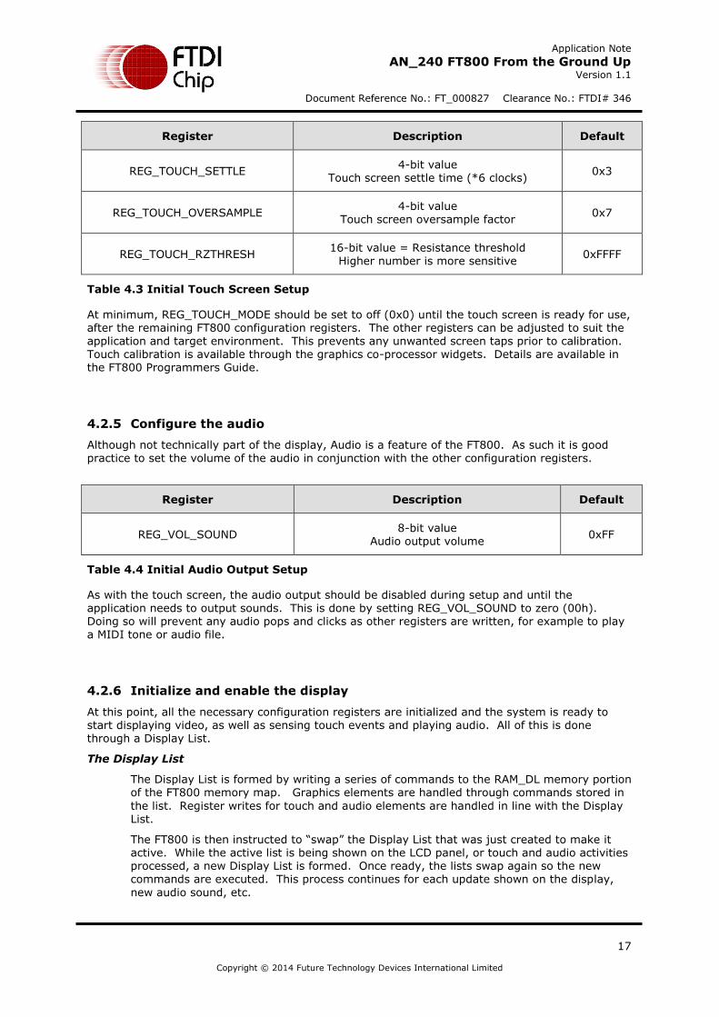
Register Description Default
REG_TOUCH_MODE
2-bit value 0x0 = off
0x1= one-shot (one acquisition per write)
0x2 = frame sync 0x3 = continuous
0x3
REG_TOUCH_ADC_MODE 1-bit value
0x0 = single-ended (low power) 0x1 = differential (greater accuracy)
0x1
REG_TOUCH_CHARGE 16-bit value
Touch screen charge time (*6 clocks) 0x1770
Application Note
AN_240 FT800 From the Ground Up Version 1.1 Document Reference No.: FT_000827 Clearance No.: FTDI# 346
17
Copyright © 2014 Future Technology Devices International Limited
Register Description Default
REG_TOUCH_SETTLE 4-bit value
Touch screen settle time (*6 clocks) 0x3
REG_TOUCH_OVERSAMPLE 4-bit value
Touch screen oversample factor 0x7
REG_TOUCH_RZTHRESH 16-bit value = Resistance threshold
Higher number is more sensitive 0xFFFF
Table 4.3 Initial Touch Screen Setup
At minimum, REG_TOUCH_MODE should be set to off (0x0) until the touch screen is ready for use, after the remaining FT800 configuration registers. The other registers can be adjusted to suit the
application and target environment. This prevents any unwanted screen taps prior to calibration. Touch calibration is available through the graphics co-processor widgets. Details are available in the FT800 Programmers Guide.
4.2.5 Configure the audio
Although not technically part of the display, Audio is a feature of the FT800. As such it is good practice to set the volume of the audio in conjunction with the other configuration registers.
Register Description Default
REG_VOL_SOUND 8-bit value
Audio output volume 0xFF
Table 4.4 Initial Audio Output Setup
As with the touch screen, the audio output should be disabled during setup and until the application needs to output sounds. This is done by setting REG_VOL_SOUND to zero (00h). Doing so will prevent any audio pops and clicks as other registers are written, for example to play a MIDI tone or audio file.
4.2.6 Initialize and enable the display
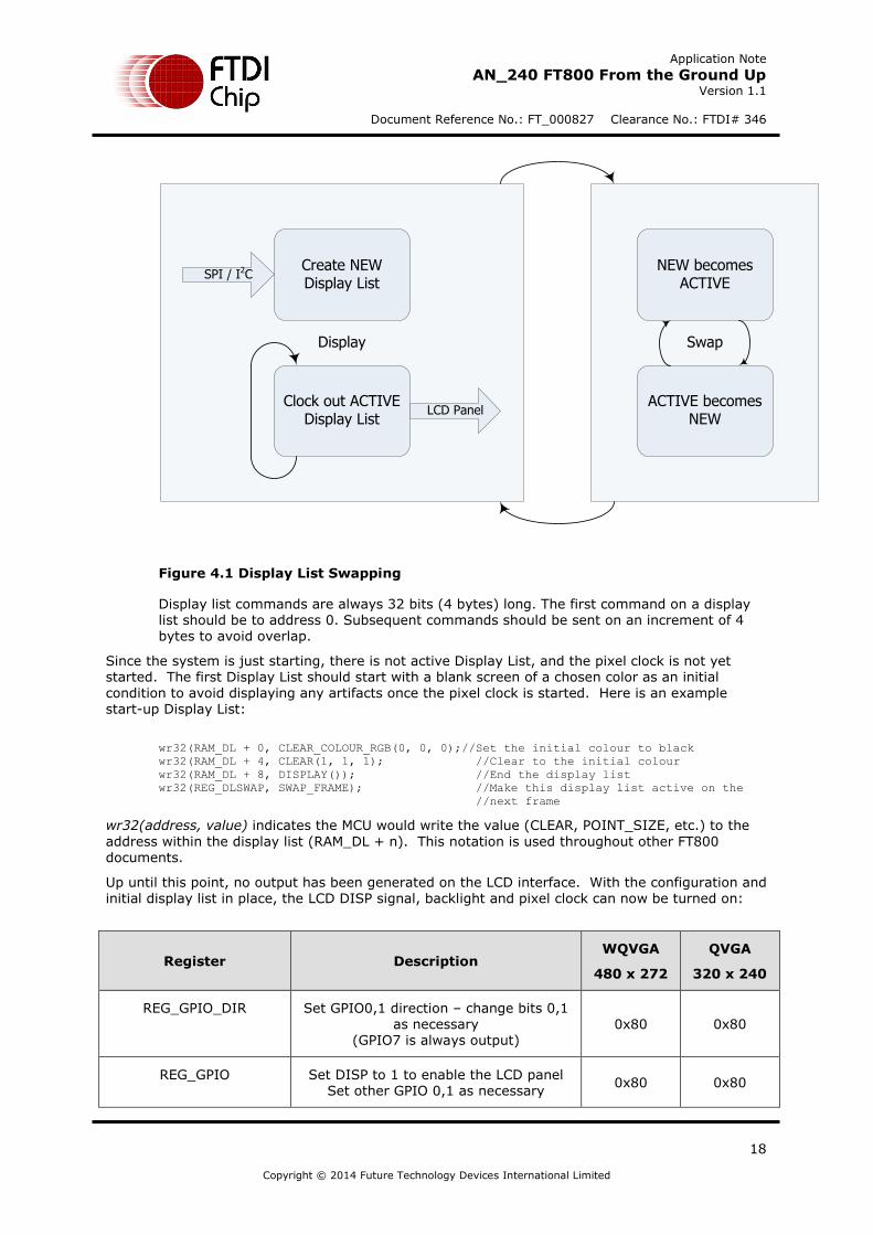
At this point, all the necessary configuration registers are initialized and the system is ready to start displaying video, as well as sensing touch events and playing audio. All of this is done through a Display List.
The Display List
The Display List is formed by writing a series of commands to the RAM_DL memory portion of the FT800 memory map. Graphics elements are handled through commands stored in
the list. Register writes for touch and audio elements are handled in line with the Display List.
The FT800 is then instructed to “swap” the Display List that was just created to make it active. While the active list is being shown on the LCD panel, or touch and audio activities processed, a new Display List is formed. Once ready, the lists swap again so the new commands are executed. This process continues for each update shown on the display,
new audio sound, etc.
Application Note
AN_240 FT800 From the Ground Up Version 1.1 Document Reference No.: FT_000827 Clearance No.: FTDI# 346
18
Copyright © 2014 Future Technology Devices International Limited
Create NEW Display List
Clock out ACTIVE Display List
SPI / I2C
LCD PanelACTIVE becomes
NEW
NEW becomes ACTIVE
SwapDisplay
Figure 4.1 Display List Swapping
Display list commands are always 32 bits (4 bytes) long. The first command on a display list should be to address 0. Subsequent commands should be sent on an increment of 4 bytes to avoid overlap.
Since the system is just starting, there is not active Display List, and the pixel clock is not yet started. The first Display List should start with a blank screen of a chosen color as an initial
condition to avoid displaying any artifacts once the pixel clock is started. Here is an example start-up Display List:
wr32(RAM_DL + 0, CLEAR_COLOUR_RGB(0, 0, 0);//Set the initial colour to black
wr32(RAM_DL + 4, CLEAR(1, 1, 1); //Clear to the initial colour
wr32(RAM_DL + 8, DISPLAY()); //End the display list
wr32(REG_DLSWAP, SWAP_FRAME); //Make this display list active on the
//next frame
wr32(address, value) indicates the MCU would write the value (CLEAR, POINT_SIZE, etc.) to the
address within the display list (RAM_DL + n). This notation is used throughout other FT800 documents.
Up until this point, no output has been generated on the LCD interface. With the configuration and initial display list in place, the LCD DISP signal, backlight and pixel clock can now be turned on:
Register Description WQVGA
480 x 272
QVGA
320 x 240
REG_GPIO_DIR Set GPIO0,1 direction – change bits 0,1 as necessary
(GPIO7 is always output) 0x80 0x80
REG_GPIO Set DISP to 1 to enable the LCD panel Set other GPIO 0,1 as necessary
0x80 0x80
Application Note
AN_240 FT800 From the Ground Up Version 1.1 Document Reference No.: FT_000827 Clearance No.: FTDI# 346
19
Copyright © 2014 Future Technology Devices International Limited
Register Description WQVGA
480 x 272
QVGA
320 x 240
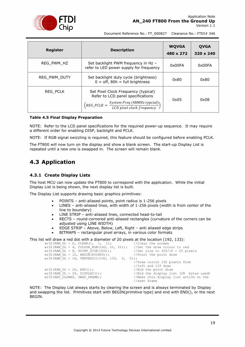
REG_PWM_HZ Set backlight PWM frequency in Hz – refer to LED power supply for frequency
0x00FA 0x00FA
REG_PWM_DUTY Set backlight duty cycle (brightness)
0 = off, 80h = full brightness 0x80 0x80
REG_PCLK Set Pixel Clock Frequency (typical) Refer to LCD panel specifications
(
)
0x05 0x08
Table 4.5 Final Display Preparation
NOTE: Refer to the LCD panel specifications for the required power-up sequence. It may require a different order for enabling DISP, backlight and PCLK.
NOTE: If RGB signal swizzling is required, this feature should be configured before enabling PCLK.
The FT800 will now turn on the display and show a blank screen. The start-up Display List is
repeated until a new one is swapped in. The screen will remain blank.
4.3 Application
4.3.1 Create Display Lists
The host MCU can now update the FT800 to correspond with the application. While the initial Display List is being shown, the next display list is built.
The Display List supports drawing basic graphics primitives:
POINTS – anti-aliased points, point radius is 1-256 pixels LINES – anti-aliased lines, with width of 1-256 pixels (width is from center of the
line to boundary)
LINE STRIP – anti-aliased lines, connected head-to-tail RECTS – round-cornered anti-aliased rectangles (curvature of the corners can be
adjusted using LINE WIDTH) EDGE STRIP – Above, Below, Left, Right – anti aliased edge strips BITMAPS – rectangular pixel arrays, in various color formats
This list will draw a red dot with a diameter of 20 pixels at the location (192, 133): wr32(RAM_DL + 0, CLEAR(1, 1, 1); //Clear the screen
wr32(RAM_DL + 4, COLOUR_RGB(160, 22, 22)); //Set the draw colour to red
wr32(RAM_DL + 8, POINT_SIZE(320)); //Set size to 320/16 = 20 pixels
wr32(RAM_DL + 12, BEGIN(POINTS)); //Start the point draw
wr32(RAM_DL + 16, VERTEX2II(192, 133, 0, 0));
//Draw circle 192 pixels from
//left and 133 down
wr32(RAM_DL + 20, END()); //End the point draw
wr32(RAM_DL + 24, DISPLAY()); //End the display list (28 bytes used)
wr32(REG_DLSWAP, SWAP_FRAME); //Make this display list active on the
//next frame
NOTE: The Display List always starts by clearing the screen and is always terminated by Display and swapping the list. Primitives start with BEGIN(primitive type) and end with END(), or the next BEGIN.
Application Note
AN_240 FT800 From the Ground Up Version 1.1 Document Reference No.: FT_000827 Clearance No.: FTDI# 346
20
Copyright © 2014 Future Technology Devices International Limited
4.3.2 Update the Display List
Subsequent changes to the display (e.g. updating an item on a menu) are done by sending a new display list over the interface to the FT800. This will be an iterative process repeated as many times as the screen requires new data. The FT800 documentation calls the Display List being built the “Update List” while the image the user can observe is on the “Active List”. Nothing new is observed until the display list is swapped over.
4.3.3 Widgets & the FT800 Graphics Engine
In addition to the primitives available through the Display List, the FT800 provides a selection of “Widgets” through its Graphics Engine. These widgets are:
TEXT – draw text of varying font types and sizes NUMBER – draw a decimal number with optional sign BUTTON – draw a button KEYS – draw a row of keys
CLOCK – draw an analog clock face
GAUGE – draw a gauge with optional pointer and tick marks DIAL – draw a knob with an optional pointer PROGRESS – draw a progress bar showing two colours SLIDER – draw a slider bar with knob SCROLLBAR – draw a scroll bar TOGGLE – draw a selection bar with two choices (yes/no, on/off, etc.)
GRADIENT – draw a smooth color gradient SPINNER – draw an animated spinner (i.e. “Please Wait”) LOGO – draw an animated FTDI logo
Other commands are available, such as SNAPSHOT (take a snapshot of the current screen), TRANSLATE (manipulate a bitmap), SKETCH (draw from the touch panel as input), LOADIMAGE (store a JPEG image) and INFLATE (decompress a file into memory). Commands are included to encapsulate Display List primitives as well. The full list of commands is available in the FT800
Programmer Guide.
These commands allow complex graphic images to be drawn with a minimum of commands and
host MCU processing.
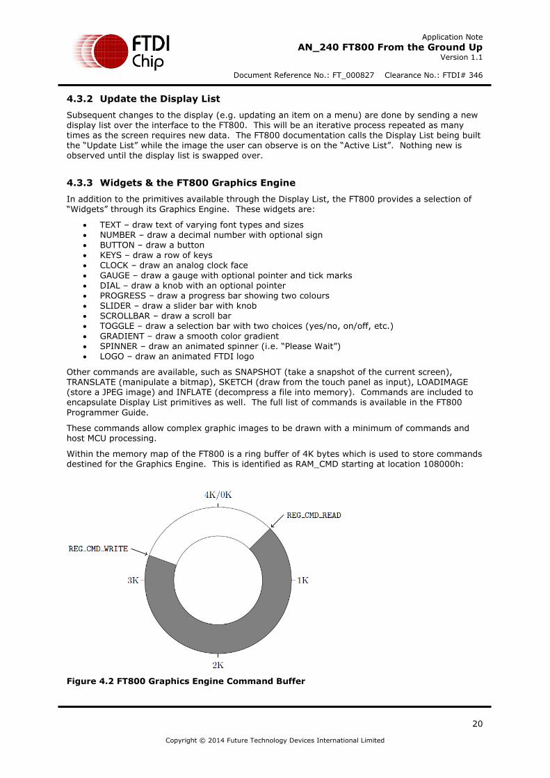
Within the memory map of the FT800 is a ring buffer of 4K bytes which is used to store commands destined for the Graphics Engine. This is identified as RAM_CMD starting at location 108000h:
Figure 4.2 FT800 Graphics Engine Command Buffer
Application Note
AN_240 FT800 From the Ground Up Version 1.1 Document Reference No.: FT_000827 Clearance No.: FTDI# 346
21
Copyright © 2014 Future Technology Devices International Limited
When idle, the values of REG_CMD_WRITE and REG_CMD_READ are equal. As commands are written to the ring buffer, the value of REG_CMD_WRITE is incremented. When the Graphics
Engine detects the difference, it will process the commands and increment REG_CMD_READ until it again matches REG_CMD_WRITE. When issuing commands, the size of the available command buffer should be checked:
Leaving one command space of 4-bytes for the freespace calculation will prevent overrun in the event the command buffer is completely full.
The graphics commands are sent to the command buffer in a similar fashion as the Display List used for primitives. In fact, Display List commands can be embedded into the Graphics Engine
command list. The following command list would perform the same function of blanking the display as the initial Display List in Section 4.2.6 above.
cmd(CMD_DLSTART); // start a new display list
cmd(CLEAR_COLOR_RGB(0, 0, 0)); // set clear color
cmd(CLEAR(1, 1, 1)); // clear screen
cmd(DISPLAY()); // end the display list
cmd(CMD_SWAP()); // swap to the new display
As with sending data for the Display List, these commands indicate to send certain bytes over the SPI or I2C interface to a particular memory location. For the example Command List shown here, the following data is written from the host MCU to the FT800:
cmdBufferRd = rd32(REG_CMD_READ); // obtain the Graphics Engine stop point
cmdBufferWr = rd32(REG_CMD_WRITE); // obtain the ring buffer starting point
if ((4096 - (cmdBufferWr – cmdBufferRd)) > 4) // enough space?
{
wr32(cmdBufferWr + 0, 0xffffff00); // CMD_DLSTART
wr32(cmdBufferWr + 4, 0x40000000); // CLEAR_COLOR_RGB with black
wr32(cmdBufferWr + 8, 0x26000007); // CLEAR color, stencil & tag buffers
wr32(cmdBufferWr + 12, 0xffffff01); // DISPLAY() to the new list
wr32(REG_CMD_WRITE, cmdBufferWr + 16); // Update the write buffer
}
Unlike the Display List, however, the Graphics Engine commands may require arguments making each write a variable length. For example, the Clock widget would take the following form:
...
// n is the the first location after the previous command
wr32(cmdBufferWr + n, 0xffffff14); // CMD_CLOCK
wr16(cmdBufferWr + n + 4, 100); // X position 100 from left
wr16(cmdBufferWr + n + 6, 120); // Y position 120 from top
wr16(cmdBufferWr + n + 8, 50); // radius of 50
wr16(cmdBufferWr + n + 10, OPT_NOSECS); // don’t display second hand
wr16(cmdBufferWr + n + 12, 8); // hour = 8
wr16(cmdBufferWr + n + 14, 15); // minute = 15
wr16(cmdBufferWr + n + 16, 0); // seconds = 0
wr16(cmdBufferWr + n + 18, 0); // milliseconds = 0
// clock command is complete
// issue the next command
wr32(cmdBufferWr + n + 20, <next command>); // issue the next command
...
Application Note
AN_240 FT800 From the Ground Up Version 1.1 Document Reference No.: FT_000827 Clearance No.: FTDI# 346
22
Copyright © 2014 Future Technology Devices International Limited
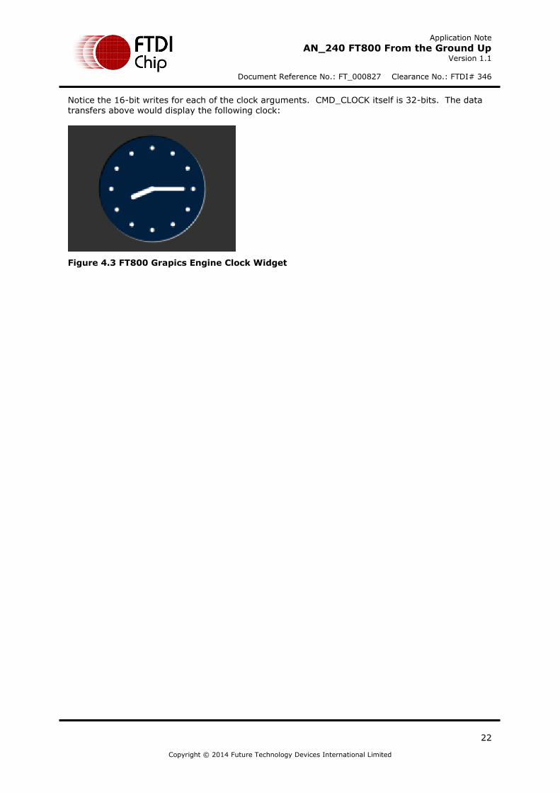
Notice the 16-bit writes for each of the clock arguments. CMD_CLOCK itself is 32-bits. The data transfers above would display the following clock:
Figure 4.3 FT800 Grapics Engine Clock Widget

Application Note
AN_240 FT800 From the Ground Up Version 1.1 Document Reference No.: FT_000827 Clearance No.: FTDI# 346
23
Copyright © 2014 Future Technology Devices International Limited
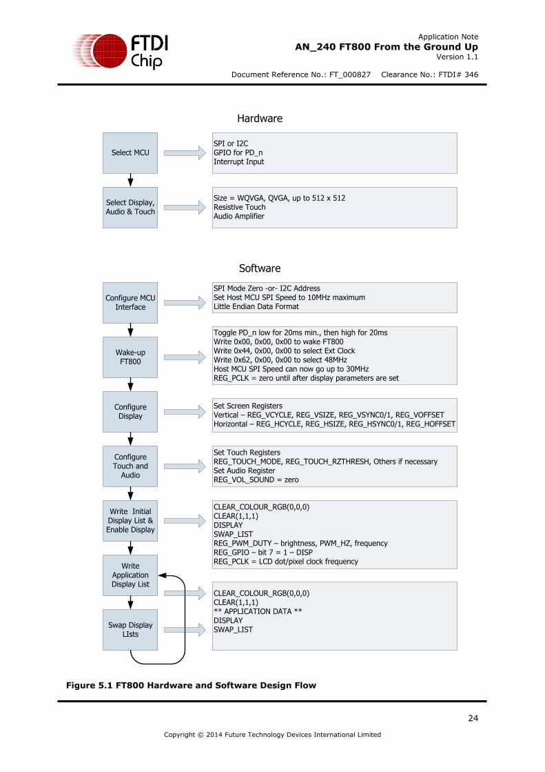
5 FT800 Design Summary
The FT800 provides an easy way to incorporate graphics displays into products providing for a lower cost solution or enabling a display into systems that could not otherwise afford this capability. With only the FT800 between the MCU and the LCD display, a vivid graphics experience with touch and audio is now possible.
The overall design flow from component selection to displaying the first screen is captured here:
Application Note
AN_240 FT800 From the Ground Up Version 1.1 Document Reference No.: FT_000827 Clearance No.: FTDI# 346
24
Copyright © 2014 Future Technology Devices International Limited
Select Display, Audio & Touch
Select MCU
Configure MCU Interface
Wake-up FT800
Configure Display
Configure Touch and
Audio
Write Initial Display List & Enable Display
Write Application Display List
Swap Display LIsts
SPI or I2CGPIO for PD_nInterrupt Input
Size = WQVGA, QVGA, up to 512 x 512Resistive TouchAudio Amplifier
SPI Mode Zero -or- I2C AddressSet Host MCU SPI Speed to 10MHz maximumLittle Endian Data Format
Toggle PD_n low for 20ms min., then high for 20msWrite 0x00, 0x00, 0x00 to wake FT800Write 0x44, 0x00, 0x00 to select Ext ClockWrite 0x62, 0x00, 0x00 to select 48MHzHost MCU SPI Speed can now go up to 30MHzREG_PCLK = zero until after display parameters are set
Set Screen RegistersVertical – REG_VCYCLE, REG_VSIZE, REG_VSYNC0/1, REG_VOFFSETHorizontal – REG_HCYCLE, REG_HSIZE, REG_HSYNC0/1, REG_HOFFSET
Set Touch Registers REG_TOUCH_MODE, REG_TOUCH_RZTHRESH, Others if necessarySet Audio RegisterREG_VOL_SOUND = zero
CLEAR_COLOUR_RGB(0,0,0)CLEAR(1,1,1)DISPLAYSWAP_LISTREG_PWM_DUTY – brightness, PWM_HZ, frequencyREG_GPIO – bit 7 = 1 – DISPREG_PCLK = LCD dot/pixel clock frequency
CLEAR_COLOUR_RGB(0,0,0)CLEAR(1,1,1)** APPLICATION DATA **DISPLAYSWAP_LIST
Hardware
Software
Figure 5.1 FT800 Hardware and Software Design Flow
Application Note
AN_240 FT800 From the Ground Up Version 1.1 Document Reference No.: FT_000827 Clearance No.: FTDI# 346
25
Copyright © 2014 Future Technology Devices International Limited
6 Collateral Support from FTDI
To assist engineers getting started with FT800 based designs there are a range of development systems provided. These include systems with and without displays; with a plastic encasement and display fitted bezel; with various screen sizes; and finally with a system host processor (Arduino/Atmel AtMega) or without a host processor.
Additional documentation is available including; the FT800 datasheet, datasheets describing the VM800 development kits, FT800 Programming Guides, Sample Application software template, and an ever-growing set of sample display code and projects. For more information consult the FTDI Website: http://www.ftdichip.com/EVE.htm
Application Note
AN_240 FT800 From the Ground Up Version 1.1 Document Reference No.: FT_000827 Clearance No.: FTDI# 346
26
Copyright © 2014 Future Technology Devices International Limited
7 Contact Information
Head Office – Glasgow, UK Future Technology Devices International Limited Unit 1, 2 Seaward Place, Centurion Business Park Glasgow G41 1HH United Kingdom Tel: +44 (0) 141 429 2777 Fax: +44 (0) 141 429 2758
E-mail (Sales) [email protected] E-mail (Support) [email protected] E-mail (General Enquiries) [email protected]
Branch Office – Taipei, Taiwan Future Technology Devices International Limited (Taiwan) 2F, No. 516, Sec. 1, NeiHu Road Taipei 114 Taiwan , R.O.C. Tel: +886 (0) 2 8791 3570 Fax: +886 (0) 2 8791 3576 E-mail (Sales) [email protected] E-mail (Support) [email protected] E-mail (General Enquiries) [email protected]
Branch Office – Tigard, Oregon, USA Future Technology Devices International Limited (USA) 7130 SW Fir Loop Tigard, OR 97223-8160 USA Tel: +1 (503) 547 0988
Fax: +1 (503) 547 0987 E-Mail (Sales) [email protected] E-Mail (Support) [email protected] E-Mail (General Enquiries) [email protected]
Branch Office – Shanghai, China Future Technology Devices International Limited (China) Room 1103, No. 666 West Huaihai Road, Shanghai, 200052 China Tel: +86 21 62351596 Fax: +86 21 62351595 E-mail (Sales) [email protected] E-mail (Support) [email protected] E-mail (General Enquiries) [email protected]
Web Site
www.ftdichip.com
System and equipment manufacturers and designers are responsible to ensure that their systems, and any Future Technology
Devices International Ltd (FTDI) devices incorporated in their systems, meet all applicable safety, regulatory and system-level
performance requirements. All application-related information in this document (including application descriptions, suggested
FTDI devices and other materials) is provided for reference only. While FTDI has taken care to assure it is accurate, this
information is subject to customer confirmation, and FTDI disclaims all liability for system designs and for any applications
assistance provided by FTDI. Use of FTDI devices in life support and/or safety applications is entirely at the user’s risk, and the
user agrees to defend, indemnify and hold harmless FTDI from any and all damages, claims, suits or expense resulting from such use. This document is subject to change without notice. No freedom to use patents or other intellectual property rights is
implied by the publication of this document. Neither the whole nor any part of the information contained in, or the product
described in this document, may be adapted or reproduced in any material or electronic form without the prior written consent
of the copyright holder. Future Technology Devices International Ltd, Unit 1, 2 Seaward Place, Centurion Business Park,
Glasgow G41 1HH, United Kingdom. Scotland Registered Company Number: SC136640
Application Note
AN_240 FT800 From the Ground Up Version 1.1 Document Reference No.: FT_000827 Clearance No.: FTDI# 346
27
Copyright © 2014 Future Technology Devices International Limited
Appendix A – References
Document References
DS_FT800 – FT800 Datasheet
PG_FT800 – FT800 Programmers Guide
AN_245 – VM800CB SampleApp PC Introduction
AN_246 – VM800CB SampleApp Arduino Introduction
Acronyms and Abbreviations
Terms Description
EMC Electromagnetic Compatibility
EVE Embedded Video Engine
GPIO General Purpose Input / Output
I2C Inter-Integrated Circuit
IC Integrated Circuit
LCD Liquid Crystal Display
MCU Microcontroller
PCM Pulse Coded Modulation
PWM Pulse Width Modulation
QVGA Quarter VGA (320 x 240 pixel display size)
SPI Serial Peripheral Interface
TFT Thin-Film Transistor
VGA Video Graphics Array
WQVGA Wide Quarter VGA (480 x 272 pixel display size)
Application Note
AN_240 FT800 From the Ground Up Version 1.1 Document Reference No.: FT_000827 Clearance No.: FTDI# 346
28
Copyright © 2014 Future Technology Devices International Limited
Appendix B – List of Tables & Figures
List of Tables
Table 3.1 FT800 Read Memory Data over SPI ....................................................................... 10
Table 3.2 FT800 Read Memory Data over I2C ........................................................................ 11
Table 3.3 FT800 Write Memory Data over SPI ....................................................................... 11
Table 3.4 FT800 Write Memory Data over I2C ....................................................................... 12
Table 3.5 FT800 Write Command over SPI ........................................................................... 12
Table 3.6 FT800 Write Command over I2C ............................................................................ 13
Table 3.7 FT800 Commands ............................................................................................... 13
Table 4.1 FT800 Memory Map ............................................................................................. 14
Table 4.2 Typical LCD Timing Parameters ............................................................................. 16
Table 4.3 Initial Touch Screen Setup ................................................................................... 17
Table 4.4 Initial Audio Output Setup .................................................................................... 17
Table 4.5 Final Display Preparation ...................................................................................... 19
List of Figures
Figure 2.1 FT800 Block Diagram ........................................................................................... 4
Figure 2.2 FT800 LCD Timing Registers – Display View ............................................................ 6
Figure 2.3 LCD RGB timing with CSPREAD disabled ................................................................. 7
Figure 2.4 LCD RGB timing with CSPREAD enabled .................................................................. 7
Figure 2.5 Example FT800 circuit .......................................................................................... 9
Figure 4.1 Display List Swapping ......................................................................................... 18
Figure 4.2 FT800 Graphics Engine Command Buffer .............................................................. 20
Figure 4.3 FT800 Grapics Engine Clock Widget ...................................................................... 22
Application Note
AN_240 FT800 From the Ground Up Version 1.1 Document Reference No.: FT_000827 Clearance No.: FTDI# 346
29
Copyright © 2014 Future Technology Devices International Limited
Appendix C – Revision History
Document Title: AN_240 FT800 From the Ground Up
Document Reference No.: FT_000827
Clearance No.: FTDI# 346
Product Page: http://www.ftdichip.com/EVE.htm
Document Feedback: Send Feedback
Revision Changes Date
1.0 Initial Release 2013-08-16
1.1 Minor update to figure 5.1 2014-06-09