bio-mems devices to monitor neural electrical circuitry andres huertas, michele panico, shuming...
Post on 22-Dec-2015
213 views
TRANSCRIPT

BIO-MEMS DEVICES TO MONITOR NEURAL ELECTRICAL CIRCUITRY
Andres Huertas, Michele Panico, Shuming Zhang
ME 381 Final Project, Dec 4th, 2003

• Planar monitoring system
• Neurons cage array
• Living chips with peptide amphiphiles gels
OUTLINE

Jenker, Müller, Fromherz, Biol. Cybern. 84, 239-249 (2001)
•Simple
•Rugged
•Easiest solution
“Future hybrid neuron-semiconductor chips will consist of complex neural networks that are directly interfaced to electronic integrated circuits. . . and may lead to novel computational facilities.”
ORIGINAL TECHNIQUE

PACKAGED CHIPS
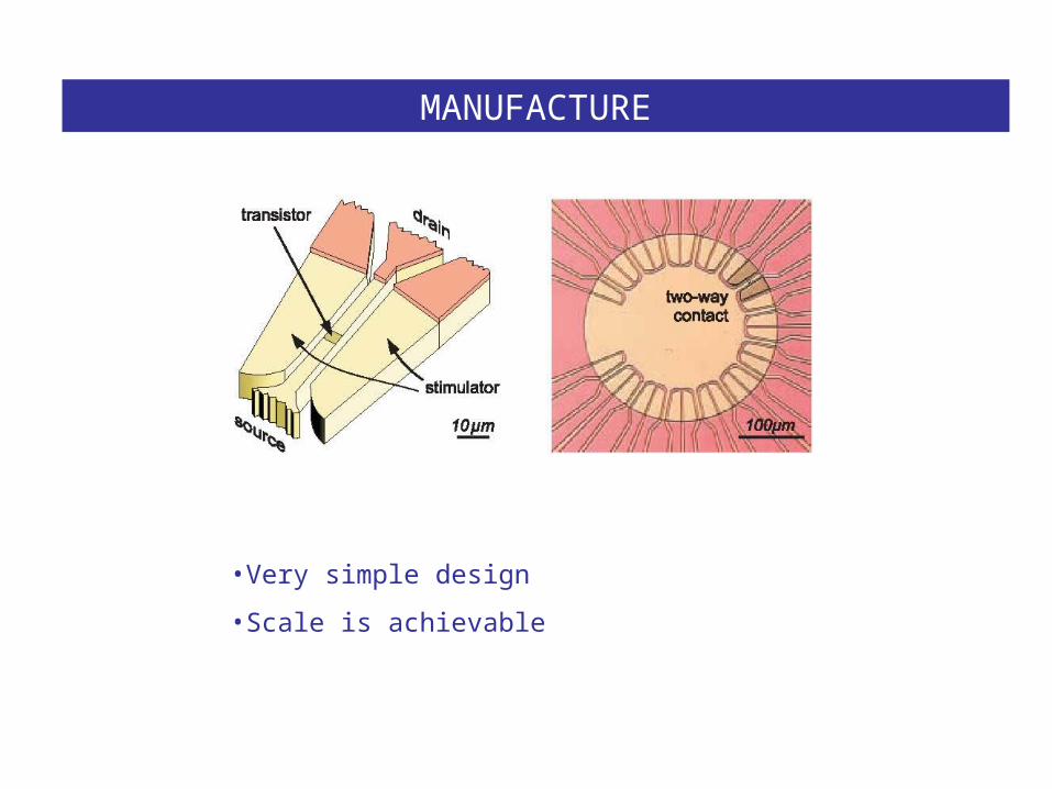
•Very simple design
•Scale is achievable
MANUFACTURE

DATA

PROCESSES GROWTH

PROBLEMS

Polyimide Picket Fences.
MANUFACTURE
Günther Zeck and Peter, Fromherz, PNAS, 2001 vol. 98, no. 18, 10457-10462

•Successful at immobilizing neurons
•Retains Functionality
MANUFACTURE

DATA

NEURO-CAGES FOR LIVE NEURAL NETWORKS STUDY
To study neural networks of individual neurons is the aim of neuroscience
Conventional technique: planar arrays of extracellular metal electrodes on which neural cultures are grown
Limitations:• Small proportion of neurons can be accessed• Neurons are mobile, thus repeated measurements of a specific neuron are difficult
Micro-cages: each neuron is trapped into one cage
Features:• Arrays of neuro-cages to allow the formation of neural networks• One-to-one correspondence between neurons and electrodes• Neurite growth is not affected by the physical confinement
Qing He., Ellis Meng, Yu-Chong Tai, Christopher M. Jerome Pine, etc, The 12th International Conference on Solid-State Sensors, Boston, MA, Jun 8-12, 2003

SILICON MICROMACHINED NEUROCHIPS
Neurochip: 1 cm square,500 µm thick silicon wafer, with a 4x4 array of wells spacedon 100 µm centers

MICROFABRICATION PROCESS
1) Composite layer of 180 nm LPCVD silicon nitride
on top of 50 nm thermal oxide is formed
2) Pattern nitride-oxide layer to define the openings
for the metal electrodes
3) 1 µm oxide step around the electrode openings
4) Nitride is stripped
5) Metallization is done using lift-off process
6) Metallization is covered by a composite insulation
Layer of 0.5 µm LTO and 1 µm PECVD nitride
7) Opening of bonding pads and alignment marks
8) EDP etching on the back using the boron-doped
layer as an etch stop
9) RIE is used to form grillwork
10) Neuron wells are formed by EDP etching to the
electrodes on the front side of the wafer
11) Removal of pad oxide at the bottom of the wells

EXPERIMENTAL RESULTS
a) Neuron sucked in pipette
b) Cell ejected from pipette
near a well
c) Pusher used to move cell
over the well
d) Cell implanted in the well
by means of the pusher
Conclusions:
• Survival rate of 75%: biocompatibility of the neurochip
• Action potentials arising from individual neurons
detected with a signal-to-noise ratio of 35-70:1
Drawbacks:
• Making bulk micromachined wells is very complicated
• Neurites growing out on the top of the well tend to pull
neuron away

PARYLENE NEURO-CAGES
Advantages of parylene:
• Non-toxic, extremely inert, resistant to moisture
and most chemicals, and biocompatible
• Its conformal deposition makes it easy to fabricate
3D structures like neuro-cage
• It is transparent: neurons can be seen through the
cages
The cage consists of a top loadingaccess hole, the cage body, and6 thin channels for neuriteovergrowth

MICROFABRICATION PROCESS
1) Oxide layer is grown on silicon wafer
2) Channel height controlling sacrificial layer is patterned
3) Two parylene and one photoresist layers are used to
form the cage
4) The sacrificial materials are removed to release the
microcage

To improve the adhesion of the cages to the substrate:
• Mechanically anchoring parylene to substrate using DRIE
• To roughen the anchoring area with short time etching in BrF3 or XeF2
PARYLENE-TO-OXIDE ADHESION

EXPERIMENTAL RESULTS
Conclusions:
• Parylene has been shown to be biocompatible
• The parylene neurocages are mechanically
functional

PA gels with trapped cells
BUILDING LIVING NEURON CHIP WITH PA GELS

silicon
photoresist
cast PDMS
replica molding replica molded microwells
Poly(dimethylsiloxane) Substrates

PEPTIDE AMPHIPHILE
Hartgerink, J.D., E. Beniash, and S.I. Stupp, Science, 2001. 294(5547): p. 1684-1688.

PDMS
O2 Plasma
MEMBRANE PATTERNING

Si
SU8SU8 SU8 SU8 SU8 SU8 SU8SU8
SU8-2025 Separation layer
PDMS membrane layer
Bulk PDMS
SELF REGISTRATED MEMBRANE PATTERNING

• Professor Horacio D. Espinosa
• TA: Yong Zhu
• Team members
ACKNOWLEDGEMENT