asynchronous design using commercial hdl synthesis tools michiel ligthart karl fant ross smith...
Post on 19-Dec-2015
218 views
TRANSCRIPT
Asynchronous Design Using Asynchronous Design Using Commercial HDL Synthesis ToolsCommercial HDL Synthesis Tools
Michiel Ligthart
Karl Fant
Ross Smith
Alexander Taubin
Alex Kondratyev

OutlineOutline
Added Value of NCL - Simplification of design Added Value of NCL - Simplification of design
Canonical form of gates - The key for optimizationCanonical form of gates - The key for optimization
NCL in CAD flow. An exampleNCL in CAD flow. An example
Validation of optimizationValidation of optimization
Experimental resultsExperimental results
Conclusion and future workConclusion and future work

Inherent to asynchronousInherent to asynchronous- no clock system- low EMI- free stand-by mode, etc.
Particular to NULL Convention Logic (NCL)Particular to NULL Convention Logic (NCL)- ease of design (reduced time to market) use standard HDL and commercial tools to use standard HDL and commercial tools to
simulate and synthesize asynchronous circuitssimulate and synthesize asynchronous circuits
- nicely fits current/future (DSM) technology
Inherent to delay-insensitiveInherent to delay-insensitive
- easy to reuse design- plug-’n’-play SoC design- easily portable among technologies
Potential NCL AdvantagesPotential NCL Advantages

OutlineOutline
Added Value of NCL - Simplification of designAdded Value of NCL - Simplification of design
Canonical form of gates - The key for optimizationCanonical form of gates - The key for optimization
NCL in CAD flow. An exampleNCL in CAD flow. An example
Validation of optimizationValidation of optimization
Experimental resultsExperimental results
Conclusion and future workConclusion and future work

NULL
Data Communication Based on DI Data Communication Based on DI EncodingEncoding
Completiondetection
Combinational
circuitry
Request for DATA/NULL
• DIprotocolwithspacer(NULL)– NULL propagation / NULL acknowledge – Data propagation / Data acknowledge
Reg
ister
Reg
ister
DATACompletion by codeword
Logic gate
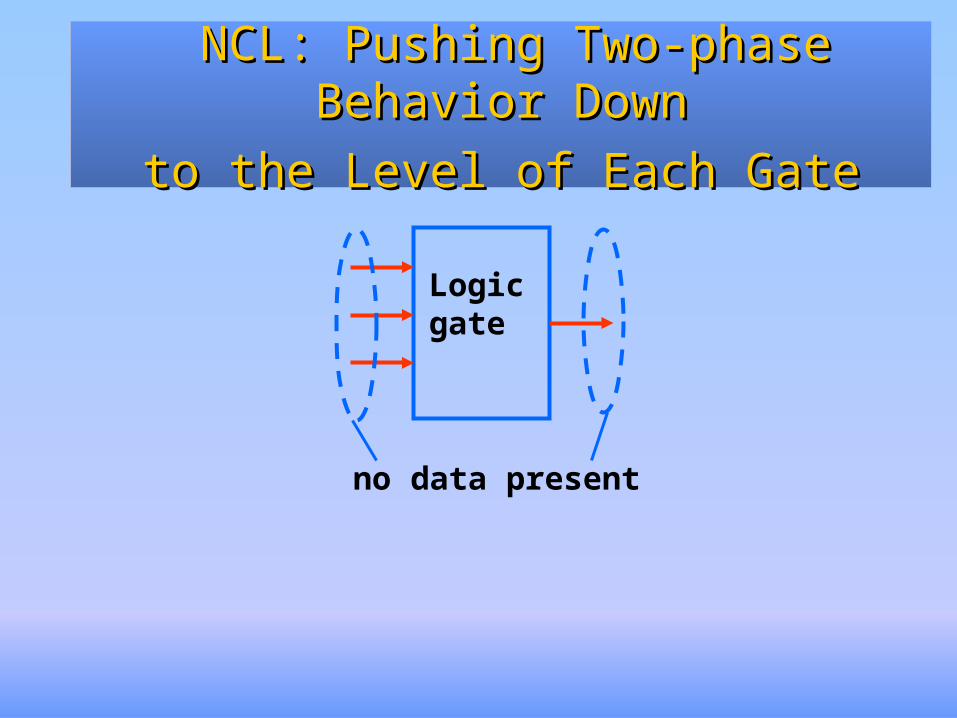
no data present
NCL:NCL: Pushing Two-phase Behavior DownPushing Two-phase Behavior Down
to the Level of Each Gateto the Level of Each Gate
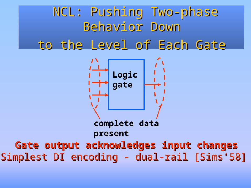
Logic gate
complete data present
NCL:NCL: Pushing Two-phase Behavior DownPushing Two-phase Behavior Down
to the Level of Each Gateto the Level of Each Gate
Gate output acknowledges input changesGate output acknowledges input changesSimplestDIencoding-dual-rail[Sims’58]SimplestDIencoding-dual-rail[Sims’58]
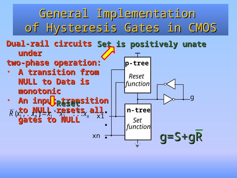
General Implementation General Implementation of Hysteresis Gates in CMOSof Hysteresis Gates in CMOS
p-tree
n-tree
Set function
functionReset
. . .x1
xn
g
g=S+gRg=S+gR
Dual-rail circuits underDual-rail circuits undertwo-phase operation:two-phase operation:• A transition from NULL to A transition from NULL to
Data is monotonicData is monotonic• An input transition to An input transition to
NULL resets all gates to NULL resets all gates to NULLNULL
nn xxxxxR ...),...,( 211
Set is positively unateSet is positively unate
Reset Reset
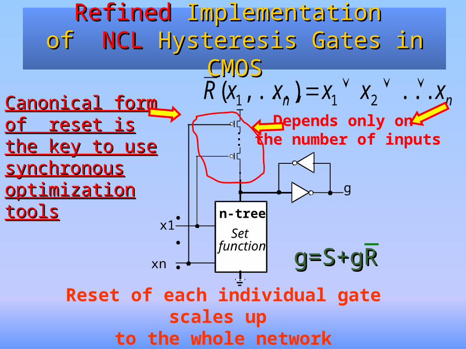
RefinedRefined Implementation Implementation of of NCLNCL Hysteresis Gates in CMOS Hysteresis Gates in CMOS
n-tree
Set function. .
.x1
xn
g
nn xxxxxR ...),...,( 211
Depends only on the number of inputs
Canonical form of Canonical form of reset is the key to reset is the key to use synchronous use synchronous optimization toolsoptimization tools
Reset of each individual gate scales up to the whole network
g=S+gRg=S+gR

RoomforRoomforoptimizationoptimization
2 2
3
2
3
4
2
3
4
5
11 1 1
M of N threshold gates with hysteresis behavior
C-element equivalents
OR gate equivalents
DIMS[Muller’62][Sparso’92]
Family of Logic GatesFamily of Logic Gates
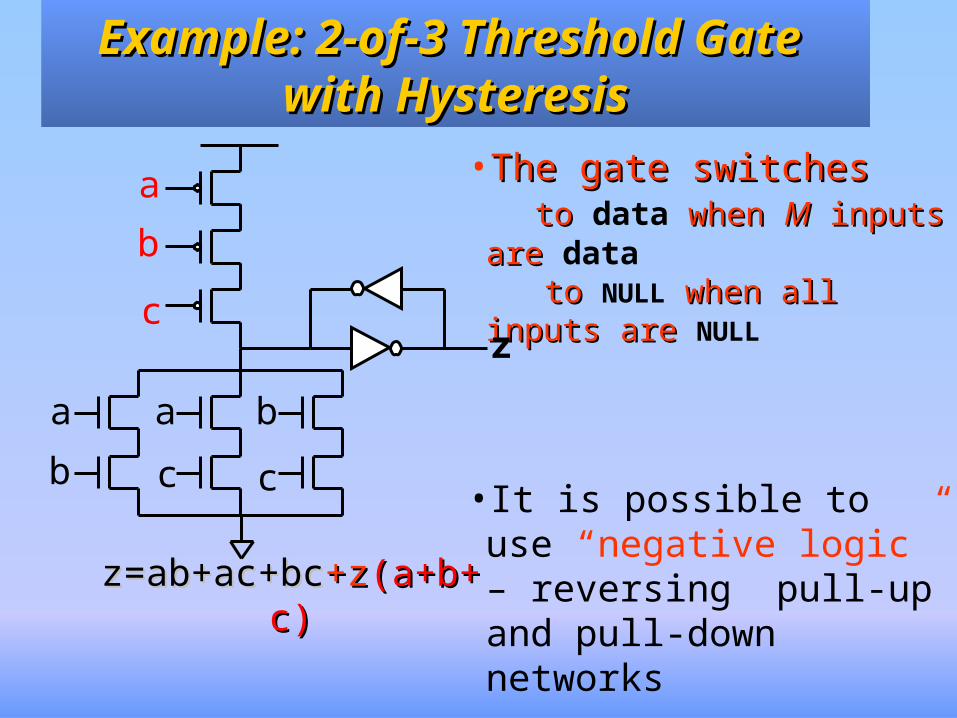
z=ab+ac+bcz=ab+ac+bc+z+z(a+b+c)(a+b+c)
• The gate switchesThe gate switches to to data when when MM inputs are inputs are data toto NULL when all inputs arewhen all inputs are NULL
• It is possible to use “negative logic” – reversing pull-up and pull-down networks
a
b
b
b
c
c
a
a
z
Example: 2-of-3 Threshold Gate Example: 2-of-3 Threshold Gate with Hysteresiswith Hysteresis
c
OutlineOutline
Added Value of NCL - Simplification of design Added Value of NCL - Simplification of design
Canonical form of gates - The key for optimizationCanonical form of gates - The key for optimization
NCL in CAD flow. An exampleNCL in CAD flow. An example
Validation of optimizationValidation of optimization
Experimental resultsExperimental results
Conclusion and future workConclusion and future work

RTL Design Flow – RTL Design Flow – Combinational OptimizationCombinational Optimization
SeparatecombinationallogicandregistersSeparatecombinationallogicandregisters
Request for data/nullreset
Combi-national
process
Request for data/nullS
eque
ntia
lpr
oces
s
Replaced by NCL Replaced by NCL registration in RTL coderegistration in RTL codeSubject of Subject of
synthesis and synthesis and optimizationoptimization
The topic of this The topic of this presentationpresentation

NCLNCLlibrarylibrary
VHDL
Genericlibrary
Synthesis
Dual-railDual-raildefinitiondefinition
Intermediatenetlist
NCLNCLnetlistnetlist
Synthesis
Step 1. Step 1. Translate HDL into Translate HDL into
“synchronous” netlist“synchronous” netlist
Step 2.Step 2. Convert intermediate Convert intermediate
netlist into NCL netlistnetlist into NCL netlist
Two-Step Synthesis FlowTwo-Step Synthesis Flow (Using Synopsys' Design Compiler)(Using Synopsys' Design Compiler)

• RTLdescription(MUX)
entity test input a,b,s : ncl_logic; output z : ncl_logic;architectureprocess (a, b, s) is begin if s = ‘1’ then z <= a; else z <= b; end if;end process;
ab
s
z
Input to Step 1: RTL DescriptionInput to Step 1: RTL Description(Multiplexer Example)(Multiplexer Example)

MUX Example: Output of Step 1 / Input MUX Example: Output of Step 1 / Input to Step 2: Intermediate Netlistto Step 2: Intermediate Netlist
a
s
b
x
y
z
Two input NAND gates
ab
s
z
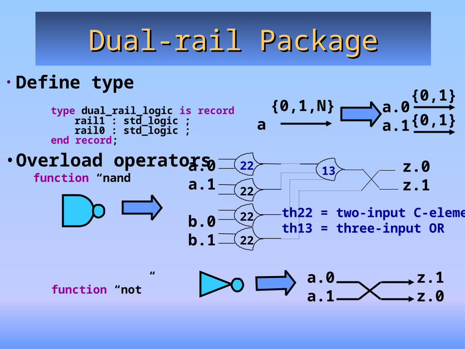
Dual-rail PackageDual-rail Package• Define type
type dual_rail_logic is record rail1 : std_logic ; rail0 : std_logic ; end record;
a.0a.1
{0,1}
{0,1}a{0,1,N}
function “not”a.0a.1
z.1z.0
• Overload operators 22
22
22
22
13 z.0z.1
a.0a.1
b.0b.1
function “nand”
th22 = two-input C-elementth13 = three-input OR

Optimizing with Design CompilerOptimizing with Design Compiler
Dual-rail expansion
Two phases (set and reset) are separated
Set phase ensures circuit functionality
Reset phase is implied
Optimizations are applied to the set phase

Dual-rail Dual-rail ExpansionExpansion ofof MUX MUX
a
s
b
x
y
z
Naive semi-static DIMS implementation – 114 transistors (can be reduced to 63 transistors by merging C-elements with OR-gates) versus 14 for a synchronous circuit
b.f
a.t
b.tD-R
NAND
D-RNAND
D-RNAND
x.t
s.f
a.f
x.f
y.t
y.f
z.t
z.f
s.t
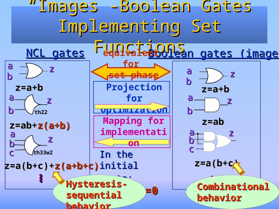
““Images”-Boolean Gates Images”-Boolean Gates Implementing Set FunctionsImplementing Set Functions
NCL gatesNCL gates
z=ab+z=ab+z(a+b)z(a+b)
aa
bb th22
zz
aa
aabb
zz
z=a+bz=a+b
z=a(b+c)+z=a(b+c)+z(a+b+c)z(a+b+c)
bbcc th33w2
zz
……
Boolean gates (images)Boolean gates (images)
z=abz=abaa
aabb
zz
z=a+bz=a+b
z=a(b+c)z=a(b+c)
aa
bbzz
bbcc
zz
……equivalent for
set phase
In the initial state:In the initial state: z=a=b=c=0z=a=b=c=0
Hysteresis-Hysteresis-sequential behaviorsequential behavior
Combinational Combinational behaviorbehavior
Projection for optimization
Mapping for implementation
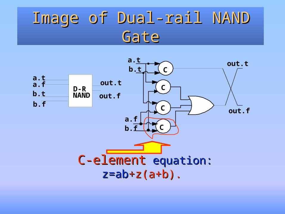
Image of Dual-rail NAND GateImage of Dual-rail NAND Gate
out.t
out.f
C
C
C
C
a.tb.t
a.fb.f
D-RNAND
a.ta.fb.t
b.f
C-elementC-element equation: z=abequation: z=ab++z(a+b). z(a+b).
out.t
out.f
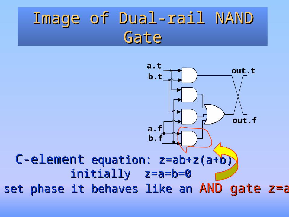
Image of Dual-rail NAND GateImage of Dual-rail NAND Gate
out.t
out.f
a.tb.t
a.fb.f
C-elementC-element equation: z=ab+z(a+b), equation: z=ab+z(a+b), initially z=a=b=0initially z=a=b=0
In a set phase it behaves like anIn a set phase it behaves like an AND gateAND gate z=abz=ab
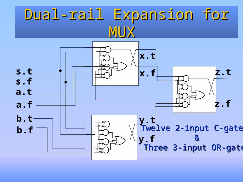
Dual-rail Dual-rail ExpansionExpansion forfor MUX MUX
b.f
a.t
b.t
x.t
s.f
a.f
x.f
y.t
y.f
z.t
z.f
s.t
Twelve 2-input C-gates Twelve 2-input C-gates &&
Three 3-input OR-gatesThree 3-input OR-gates
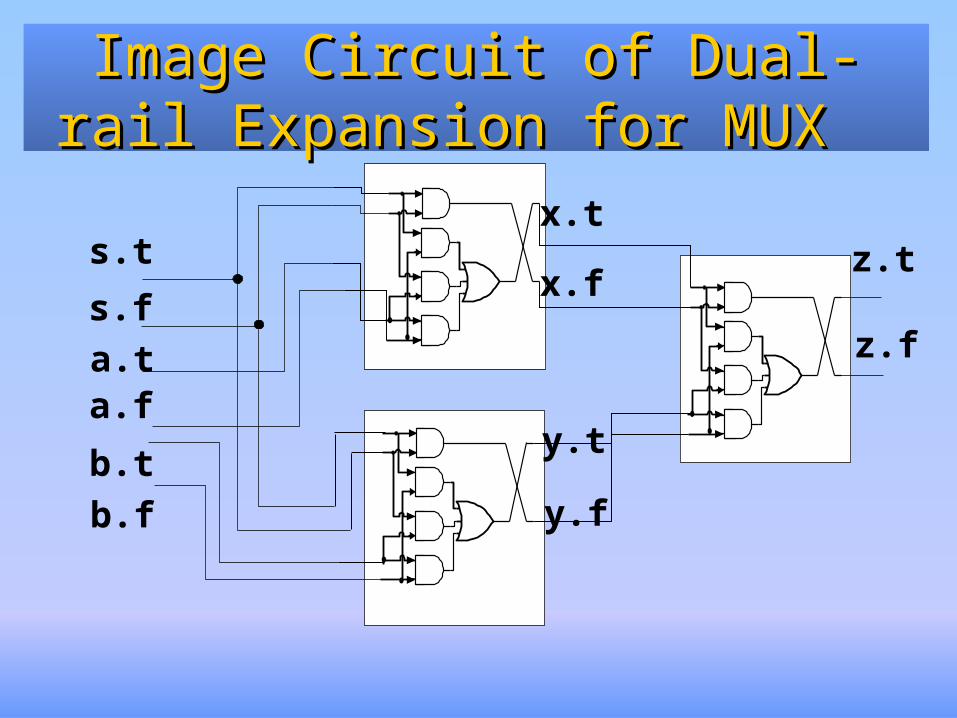
Image Circuit of Dual-rail Image Circuit of Dual-rail ExpansionExpansion forfor MUX MUX
b.f
a.t
b.t
x.t
s.f
a.f
x.f
y.t
y.f
z.t
z.f
s.t

Optimized with Design Compiler Optimized with Design Compiler
MUX circuit passes technology independent optimization and is mapped to “images” of gates from NCL library.
b.f
a.t
b.t
s.f
a.f
s.t
z.t
z.f
image of th33w2
A(B+C)A(B+C)
image of thXORAB+CDAB+CD

Technology Mapping with Design Technology Mapping with Design Compiler Compiler
NCL circuit: images are replaced by gates withimages are replaced by gates with hysteresishysteresis
b.f
a.t
b.t
s.f
a.f
s.t
thXOR
z.t
z.f
th33w2
th33w2th33w2
thXOR
2
2
thXORthXOR2
2
th22
th22
th24w2
th24w2
f
e
m
n
e
f
m
n
k
Semi-static CMOS Semi-static CMOS implementation of implementation of thXOR.thXOR.
44 transistors - 30% better than optimized DIMS

OutlineOutline
Added Value of NCL - Simplification of design Added Value of NCL - Simplification of design
Canonical form of gates - The key for optimizationCanonical form of gates - The key for optimization
NCL in CAD flow. An exampleNCL in CAD flow. An example
Validation of optimizationValidation of optimization
Experimental resultsExperimental results
Conclusion and future workConclusion and future work

Optimization FlowOptimization Flow
Booleancircuit
Dual-railimage
translation
Optimizedcircuit
optimization
Mappedtoimages
dual-rail
package
Design
compiler
Design
compiler
tech.mapping
Synchronous
DIMS circuit
Hysteresis gates
DIDIequivalenceequivalence
Asynchronous
Virtual objectVirtual object
Real objectReal object

Validation of OptimizationValidation of Optimization
Thevalidityoftransformations(DIequivalenceDIequivalence)isbasedontwoproperties:
FunctionalequivalenceFunctionalequivalenceofoptimizedandoriginalcircuits(undertwo-phaseoperation)
MaintenanceofDIpropertiesMaintenanceofDIpropertiesinoptimizedcircuit
BotharebasedonthepropertiesofBotharebasedonthepropertiesofprimeandprimeandirredundantnetworksirredundantnetworksandpropertiesandpropertiesofalgebraicofalgebraicfactorizationfactorization[Brayton’90,Hachtel’92][Brayton’90,Hachtel’92]
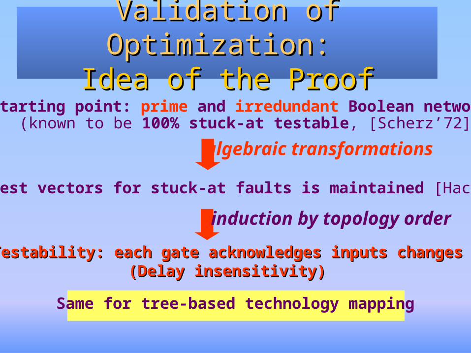
Starting point: prime and irredundant Boolean network(known to be 100% stuck-at testable, [Scherz’72])
algebraic transformations
Set of test vectors for stuck-at faults is maintained [Hachtel’92]
induction by topology order
Testability: each gate acknowledges inputs changesTestability: each gate acknowledges inputs changes(Delay insensitivity)(Delay insensitivity)
Same for tree-based technology mapping
Validation of Optimization: Validation of Optimization: Idea of the ProofIdea of the Proof

OutlineOutline
Added Value of NCL - Simplification of design Added Value of NCL - Simplification of design
Canonical form of gates - The key for optimizationCanonical form of gates - The key for optimization
NCL in CAD flow. An exampleNCL in CAD flow. An example
Validation of optimizationValidation of optimization
Experimental resultsExperimental results
Conclusion and future workConclusion and future work

Manual vs. Synthesized DesignsManual vs. Synthesized Designs
0
500
1000
1500
2000
2500
3000
3500
4000
4500
ManualSynthesized
Area (transistor number)
For bigger circuits Synthesis/Manual ratio is better For bigger circuits Synthesis/Manual ratio is better (22% improvement for biggest example) (22% improvement for biggest example)
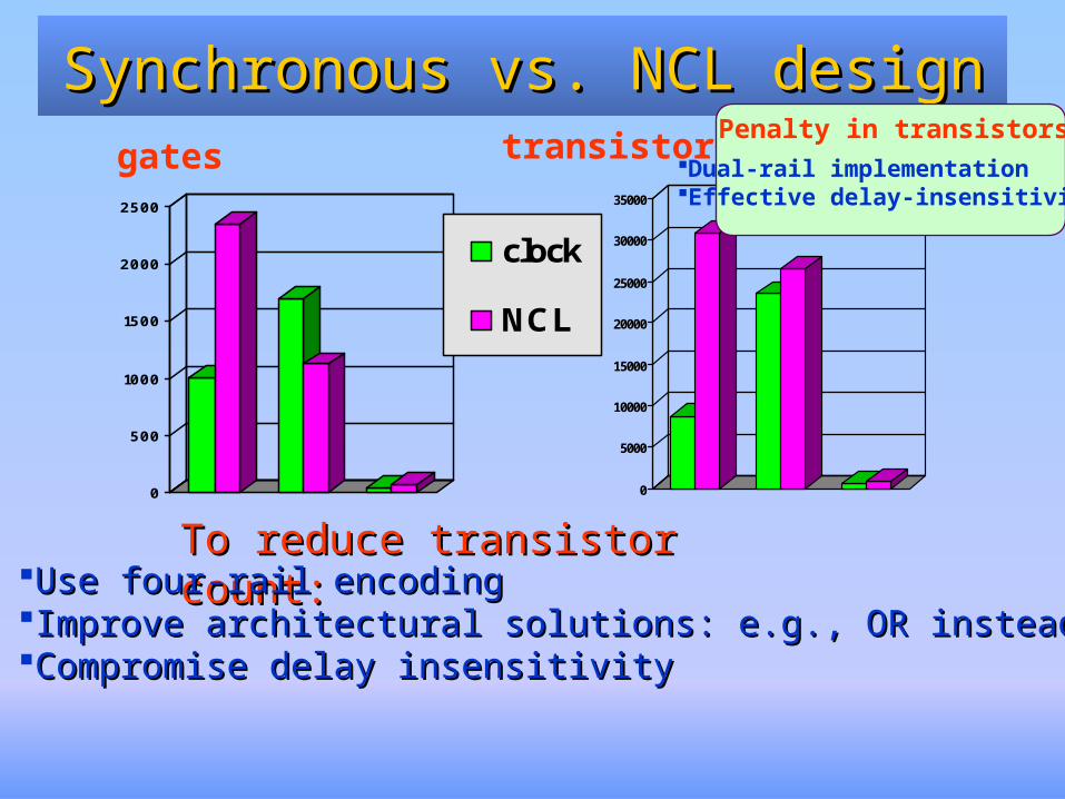
Synchronous vs. NCL design Synchronous vs. NCL design
0
500
1000
1500
2000
2500
clock
NCL
0
5000
10000
15000
20000
25000
30000
35000
gates transistorsPenalty in transistors:
Dual-rail implementationEffective delay-insensitivity
To reduce transistor count:To reduce transistor count:Use four-rail encodingUse four-rail encodingImprove architectural solutions: e.g., OR instead MUXImprove architectural solutions: e.g., OR instead MUXCompromise delay insensitivityCompromise delay insensitivity

OutlineOutline
Added Value of NCL - Simplification of design Added Value of NCL - Simplification of design
Canonical form of gates - The key for optimizationCanonical form of gates - The key for optimization
NCL in CAD flow. An exampleNCL in CAD flow. An example
Validation of optimizationValidation of optimization
Experimental resultsExperimental results
Conclusion and future workConclusion and future work

ConclusionsConclusions
• FirstmethodologytousestandardHDLFirstmethodologytousestandardHDLandcommercialtoolsbothtosimulateandandcommercialtoolsbothtosimulateandsynthesizeasynchronouscircuitssynthesizeasynchronouscircuits
• ThemethodologyisformallyvalidatedThemethodologyisformallyvalidated
• TheresultsofthesynthesisareacceptableTheresultsofthesynthesisareacceptable

Future TasksFuture Tasks
Reducearea/powerReducearea/powerwithoutlosingdelayinsensitivitywithoutlosingdelayinsensitivity(e.g.,four-raildesign)(e.g.,four-raildesign)
RelaxDIrequirementstoreducearea(e.g.,usingRelaxDIrequirementstoreducearea(e.g.,usingtimingassumptionstimingassumptions))
UseUse peepholepeepholeoptimizationsoptimizations(e.g.,(e.g.,mergegatesmergegatesusedusedforregistrationwiththeirinputgatesetc.)forregistrationwiththeirinputgatesetc.)
WriteDesignWarecomponentstogetbetterWriteDesignWarecomponentstogetbetterperformanceforarithmeticunits(inferperformanceforarithmeticunits(inferhanddesignedhanddesignedcomponentscomponents))