applications of photocurable pmms thiol− ene stamps in soft lithography
TRANSCRIPT
pubs.acs.org/cmPublished on Web 10/14/2009r 2009 American Chemical Society
Chem. Mater. 2009, 21, 5319–5326 5319DOI:10.1021/cm902506a
Applications of Photocurable PMMS Thiol-Ene Stamps in
Soft Lithography
Luis M. Campos,† Tu T. Truong,‡ Dong Eun Shim,§ Michael D. Dimitriou,†
Daniel Shir,‡ Ines Meinel, ) Jeffrey A. Gerbec, ) H. Thomas Hahn,§
John A. Rogers,‡ and Craig J. Hawker*,†
†Materials Research Laboratory, Mitsubishi Chemical Center for Advanced Materials, Department ofChemistry and Biochemistry, and Materials Department, University of California, Santa Barbara,
California 93106, ‡Department of Chemistry, Department of Materials Science and Engineering, andDepartment of Electrical and Computer Engineering, Beckman Institute and Frederick Seitz Materials
Research Laboratory, University of Illinois at Urbana-Champaign, Urbana, Illinois 61801,§Department of Mechanical and Aerospace Engineering and Multifunctional Composites Laboratory,University of California, Los Angeles, California 90095, and )MC Research and Innovation Center,
601 Pine Avenue, Goleta, California 93117
Received August 14, 2009. Revised Manuscript Received September 28, 2009
We report the performance and characterization of a material based on poly[(3-mercaptopropyl)-methylsiloxane] (PMMS) in various soft lithography applications. PMMS stamps were made bycross-linking with triallyl cyanurate and ethoxylated (4) bisphenol A dimethacrylate via thiol-enemixed-mode chemistry. The surface chemistry of thematerials was characterized byXPSwhen variedfrom hydrophilic through oxygen plasma treatment, to hydrophobic by exposure to a fluorinatedtrichlorosilane agent. The materials are transparent above 300 nm and thermally stable up to 225 �C,thus rendering them capable to be employed in step-and-flash imprint lithography, nanoimprintlithography, nanotransfer printing, and proximity-field nanopatterning. The successful patternreplication from the micrometer to sub-100 nm scale was demonstrated.
Introduction
Nanoimprinting techniques continue to attract consi-derable interest because of their potential to enable massproduction of nanopatterns and nanostructures at lowcost and submicrometer resolution.1,2 Traditional nano-imprint lithography (NIL), developed by Chou and co-workers,3 takes advantage of themoldable characteristicsof polymermelts by heating a polymer film above its glasstransition temperature (Tg), while being pressed with atopographically patterned hard master. Upon cooling,the thermoplastic polymermaintains the inverse structureof the master. With this technology, the mold is generallya hard material, such as a silicon wafer or a metal toprevent any deformation of the patterned features duringthe imprint process. As an alternative to traditional NIL,step and flash imprint lithography (SFIL) was developedby Willson and co-workers.4 SFIL utilizes UV light tocure a thin film photoresist while being pressed with thepatterned master, thus allowing the imprinting step to bedone in the absence of high temperatures. Another major
advantage provided by this technique is the ability tooptically align the master with the template to control thespatial location of imprinted patterns. However, a pat-terned quartz master is necessary to allow UV light topenetrate the master and cure the photoresist. To avoidthe complications that arise from using hard, specialtymasters (such as quartz), soft lithography emerged as alow-cost, high throughput alternative that takes advan-tage of a single master to fabricate myriad disposablepolymeric replicas.5,6 To further enable this technology,we have recently introduced a new family of inexpensive,cross-linkable soft materials capable of replicatinghigh fidelity sub-100 nm features with curing times of1-2 min.7 In this manuscript we report the use of thesesystems in traditional soft lithographic applications, andwe characterize the physical properties that are relevantfor the viability of these processes.Soft lithography involves the fabrication of an inverse
replica of a patterned hard master using cross-linkablepolymeric materials.8,9 Generally, a liquid mixture of
*Corresponding author. E-mail: [email protected].(1) Menard, E.;Meitl, M. A.; Sun, Y.; Park, J. U.; Shir, D. J. L.; Nam,
Y. S.; Jeon, S.; Rogers, J. A. Chem. Rev. 2007, 107, 1117–1160.(2) del Campo, A.; Arzt, E. Chem. Rev. 2008, 108, 911–945.(3) Chou, S. Y.; Krauss, P. R.; Renstrom, P. J. Science 1996, 272,
85–87.(4) Colburn, M.; Johnson, S. C.; Stewart, M. D.; Damle, S.; Bailey,
T.C.; Choi, B.;Wedlake,M.;Michaelson, T. B.; Sreenivasan, S.V.;Ekerdt, J. G.; Willson, C. G. Proc. SPIE 1999, 3676, 379–389.
(5) Xia,Y.;Kim,E.;Zhao,X.-M.;Rogers, J.A.; Prentiss,M.;Whitesides,G. M. Science 1996, 273, 347–349.
(6) Xia, Y.; Whitesides, G. M. Angew. Chem., Int. Ed. 1998, 37, 550–575.
(7) Campos, L. M.; Meinel, I.; Guino, R. G.; Schierhorn, M.; Gupta,N.; Stucky, G. D.; Hawker, C. J. Adv. Mater. 2008, 20, 3728–3733.
(8) Xia, Y.; Rogers, J. A.; Paul, K. E.; Whitesides, G. M. Chem. Rev.1999, 99, 1823–1848.
(9) Gates, B. D.; Xu, Q.; Stewart, M.; Ryan, D.; Willson, C. G.;Whitesides, G. M. Chem. Rev. 2005, 105, 1171–1196.
5320 Chem. Mater., Vol. 21, No. 21, 2009 Campos et al.
small molecules and polymers is cast onto the patternedmaster and cured. The cross-linked polymeric stamp isthen peeled and further used in a wide variety of softlithography processes,1 such as soft nanoimprint litho-graphy, soft step and flash lithography, and nanotransferpritinting, among others.10 This technique allows for thefabrication of multiple, inexpensive stamps from a singlehardmaster.While several polymeric materials have beendeveloped,11-13 employing various types of cross-linkingchemistries, the most widely used are based on theplatinum catalyzed hydrosilylation of poly(dimethyl-siloxane) (PDMS). These systems are generally cured byheating but require extended periods of time, prohibitinghigh throughput fabrication. Although fast-curing sys-tems have been developed,14-16 they suffer from one ormore of the following: (a) oxygen inhibition during cross-linking, (b) high-cost materials, and (c) the use of specia-lized equipment to replicate sub-100 nm features.To avoid the above complications, materials based on
poly[(3-mercaptopropyl)methylsiloxane] (PMMS) havebeen developed for applications in soft lithography.7
PMMS can be cured via thiol-ene click chemistry witha wide array of alkene-containing cross-linkers.17 Themodularity imparted by these versatile systems allows forhigh throughput stamp fabrication and optimization ofthe resulting physical, chemical, and mechanical pro-perties.18 Furthermore, the rapid curing and molding ofthe materials via thiol-ene click chemistry can be done atambient conditions,19 without inhibition from oxygen ormoisture,20 by simply casting the prepolymer liquid mix-ture onto the patterned masters. Given the nature of thecuring chemistry, having control over the cross-linking ofthe systems allows the liquid mixture to fully infiltrate themaster molds, thus yielding high fidelity features.To study the pattern transfer capabilities of the
PMMS-based systems, we have selected the mixturecomposed of PMMS, triallyl cyanurate (TAC), andethoxylated (4) bisphenol A dimethacrylate (BPADMA,Scheme 1). The resulting cross-linked material has anelastic modulus, E, of approximately 24MPa (elongation
at break ca. 20%), and the films (ca. 0.5 mm thick) arestiffer than the commercially available PDMS (Sylgard184, E of ca. 2-3 MPa) but are also flexible, renderingthem useful in SNIL. This material has been successfullyused to pattern photonic crystals of titania21 and micro-meter arrays via microcontact printing.22
Results and Discussion
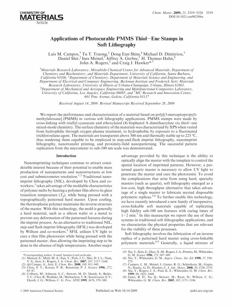
Stamp Fabrication Process. One of the most beneficialaspects of the PMMSmaterials is the ease of processing tofabricate patterned stamps (Figure 1). As previouslydescribed, the process involves the thorough mixing ofPMMS, TAC, and BPADMA, along with less than 0.1 wt% of the UV-active radical initiator DMPA (this mixtureis referred to as sample blend 2, or SB2). The liquidSB2 is then cast between an ordinary microscope glassslide and a patterned silicon master using Teflon spacersto control the thickness of the stamps (ca. 0.5 mm).It is preferred to treat the masters with the fluorinatingagent (tridecafluoro-1,1,2,2-tetrahydrooctyl)trichlorosi-lane (Cl3SiCH2CH2[CF2]5CF3, TDFOCS) by vapor de-position to enhance the release properties of the stamps.The mixture is then cured using UV light (365 nm) atambient conditions (without previous deoxygenation) for2 min (Figure 1B). Finally, the stamp is released bypeeling from the master (Figure 1C). We must note thatno pressure is required to fill the master mold inFigure 1B.16
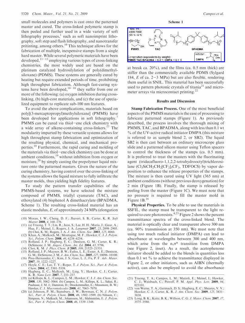
Physical Properties. To be able to use the materials inSSFIL, the stamp must be transparent to the light re-quired to cure photoresists.4,23 Figure 2 shows the percenttransmittance spectra of the cross-linked blend. Thematerial is optically clear and transparent above 300 nm(ca. 90% transmission at 350 nm). We must note thatusing too much radical initiator (DMPA) can lead toabsorbance at wavelengths between 300 and 400 nm,which arise from the n,π* transition from DMPA(see Figure 2, inset). As a result, the acetophenoneinitiator should be added to the blends in quantities lessthan 0.1 wt % to achieve the transmittance displayed inFigure 2, or other initiators, such as AIBN (thermallyactive), can also be employed to avoid the absorbance
Scheme 1
(10) Moran, I. W.; Cheng, D. F.; Jhaveri, S. B.; Carter, K. R. SoftMatter 2008, 4, 168–176.
(11) (a) Truong, T. T.; Lin, R.; Jeon, S.; Lee, H. H.;Maria, J.; Gaur, A.;Hua, F.; Meinel, I.; Rogers, J. A. Langmuir 2007, 23, 2898–2905.(b) Choi, K. M.; Rogers, J. A. J. Am. Chem. Soc. 2003, 125, 4060.
(12) Khan,A.;Malkoch,M.;Montague,M. F.;Hawker, C. J. J. Polym.Sci., Polym. Chem. 2008, 46, 6238–6254.
(13) Rolland, J. P.; Hagberg, E. C.; Denison, G. M.; Carter, K. R.;DeSimone, J. M. Angew. Chem., Int. Ed. 2004, 43, 5796.
(14) Choi, K. M. J. Phys. Chem. B 2005, 109, 21525–21531.(15) Rolland, J. P.;Maynor, B.W.; Euliss, L. E.; Exner, A. E.; Denison,
G.M.;DeSimone, J.M. J.Am.Chem.Soc. 2005, 127, 10096–10100.(16) Pina-Hernandez, C.; Kim, J. S.; Guo, L. J.; Fu, P. F. Adv. Mater.
2007, 19, 1222–1227.(17) Hoyle, C. E.; Lee, T. Y.; Roper, T. J. Polym. Sci., Part A: Polym.
Chem. 2004, 42, 5301–5338.(18) Hagberg, E. C.; Malkoch, M.; Ling, Y.; Hawker, C. J.; Carter,
K. R. Nano Lett. 2007, 7, 233–237.(19) (a)Killops,K. L.; Campos, L.M.;Hawker, C. J. J. Am.Chem. Soc.
2008, 130, 5062–5064. (b) Campos, L. M.; Killops, K. L.; Sakai, R.;Paulusse, J. M. J.; Damiron, D.; Drockenmuller, E.; Messmore, B. W.;Hawker, C. J. Macromolecules 2008, 41, 7063–7070.
(20) (a) Johnson, P. M.; Stansbury, J. W.; Bowman, C. N. J. Polym.Sci., Part A: Polym. Chem. 2008, 46, 1502–1509. (b) Nilsson, C.;Simpson, N.; Malkoch, M.; Johansson, M.; Malmstr€om, E. J. Polym.Sci., Part A: Polym. Chem. 2008, 46, 1339–1348.
(21) Truong, T. A.; Campos, L. M.; Matioli, E.; Meinel, I.; Hawker,C. J.; Weisbuch, C.; Petroff, P. M. Appl. Phys. Lett. 2009, 94,023101.
(22) vonWerne, T. A.; Germack, D. S.; Hagberg, E. C.; Sheares, V. V.;Hawker, C. J.; Carter, K. R. J. Am. Chem. Soc. 2009, 125, 3831–3838.
(23) Long, B. K.; Keitz, B. K.; Willson, C. G. J.Mater. Chem. 2007, 17,3575–3580.
Article Chem. Mater., Vol. 21, No. 21, 2009 5321
fromthe310-390nmUV-active initiator.ThePMMS-basedmaterial (SB2) is comparable to s-PDMS and h-PDMS,which are transparent to light above 300 nm.11 The newlymodified, acrylate-functional perfluoropolyether stamps(a-PFPE, an extension of the work developed by DeSi-mone and co-workers)13 reported are transparent aboveapproximately 350 nm (40% transmission at 350 nm,2 mm thick films).11
With the potential to use the PMMS materials totransfer patterns using moldable thermoplastics (such asembossing),3,24 both thermogravimetric analysis (TGA,Figure 3) and differential scanning calorimetry (DSC)were carried out to obtain information regarding thethermal stability of SB2. The TGA plot shows thatdecomposition begins to take place near 250 �C (Figure 3,bottom), a value comparable to that of Sylgard 184.25
Above 300 �C, the SB2 rapidly decomposes due to thehigh organic content from the alkene cross-linkers.Furthermore, within the temperature range from -80 to220 �C, SB2 does not undergo any phase transitions asobserved by DSC (within the lower temperature limit ofthe instrument). The result is analogous to Sylgard 184,which has a glass transition temperature (Tg) of approxi-mately -120 �C.26 The thermal stability of the PMMS
material renders it with the capability to thermally cure oremboss materials at temperatures up to approximately225 �C.Soft Step and Flash Imprint Lithography (SSFIL). The
process for SSFIL is highlighted in Figure 4, where a softstamp is used to press themoldable liquid photoresist.10,11
While applying pressure, the photoresist is then cured tomaintain the inverse pattern of the stamp. For anynanoimprint process, it is important that the resist doesnot adhere to the mold after imprinting.23 To test thecapability of SB2 to print the photoresist NXR-2010, theSSFIL procedure was carried out by applying pressurefollowed byUV light exposure (365 nm) for 1 min. As it isclearly visible from the optical microscope image inFigure 5A, the photoresist adhered to the SB2 stamp,and the pattern was ripped during the peeling process(Figure 4C).
Figure 1. Process for stamp fabrication: (A) Cast liquid SB2 onto a patterned master mold. (B) Cure the material with UV light for 2 min at ambientconditions. (C) Peel the patterned polymeric stamp.
Figure 2. Percent transmittance spectrum of a 0.5 mm thick film of SB2.The inset shows the UV-vis spectrum of DMPA in chloroform, high-lighting the nf π* transition between 310 and 380 nm.
Figure 3. Top: Complete profile of the thermogravimetric analysis(TGA) of SB2 (heating rate of 10 �C/min). Bottom: Expanded region ofthe TGA plot.
(24) King, E.; Xia, Y.; Zhao, X.-M.; Whitesides, G. M. Adv. Mater.1997, 9, 651–654.
(25) Johnson, R. T., Jr.; Biefeld, R. M.; Sayre, J. A. Polym. Eng. Sci.1984, 24, 435–441.
(26) Lahiff, E.; Leahy, R.; Coleman, J. N.; Blau, W. J.Carbon 2006, 44,1525–1529.

5322 Chem. Mater., Vol. 21, No. 21, 2009 Campos et al.
Given that PDMS materials can be modified at thesurface to become hydrophilic by exposure to oxygenplasma,27 the same treatment was applied to SB to oxidizethe surface and subsequently functionalize with the samefluorinating agent that was used for the silicon mastersand other PDMS stamps, TDFOCS.10 To characterizethe surface treatment, a nonpatterned, 2 mm thick film ofSB2 was exposed to O2 plasma for 15 s (300 mbar, 0.1 V).Longer exposure times have been shown to yield a silicalayer in PDMS, which has been exploited as an imperme-able layer to avoid deformations during SSFIL.10 How-ever, for the purpose of this work, 15 s was enough tochange thewater contact angle to<17�, as opposed to theoriginal value of 75�. A similar oxidation process wasemployed by Donzel et al. to make the surface of PDMShydrophilic after 30 s of O2 plasma treatment.27 Afterexposing the surface to TDFOCS vapor under line vacuumfor 20 min in an enclosed chamber, the water contactangle changed from <17� to 103�, rendering it hydro-phobic, in agreement with the similar treatment ofPDMS.10
The surface treatment process for SB was also char-acterized by X-ray photoelectron spectroscopy (XPS).This technique allowed for the identification of the ele-ments present at the surface before (SB2) and afterexposure to O2 plasma (SB2-OH) and after surfacefunctionalizationwith TDFOCS (SB2-F). Figure 6 showsthe evolution of the spectra at each step. From thecomposition of the blend, SB2 shows the expected pre-sence of C, N, O, S, and Si. After O2 plasma, the intensityof the O 1s peak noticeably increased in SB2-OH, relativeto the C 1s peak. Finally, the incorporation of the cova-lently boundTDFOCS is evident by the appearance of theF 1s peak at approximately 690 eV. These steps are in
accord with the observations by XPS in a similar treat-ment of PDMS.10,27
Following the procedure depicted in Figure 7 to coatthe fluorinating agent, TDFOCS, onto the surface of thepolymeric stamp, SB2-F was implemented in the SSFILprocess to pattern the photoresist NXR-2010. Under thesame conditions described earlier, the processes proved tobe successful and allowed peeling of the stamp from theprinted substrate. Minimal adhesion was experiencedwhen peeling the stamp, and the microscope image inFigure 5B does not show any imperfections.The composition chosen (SB2) has various advantages
over hard, patterned substrates, such as flexibility, lowcost, and ease of fabrication. In SSFIL/SNIL, a flexiblemold can conform to surfaces during the imprint step,thus significantly reducing defects caused by particles ordust trapped between the mold and the substrate. Giventhat pressure is applied to transfer the patterns, themechanical properties of the materials are critical inSNIL.11 Soft materials that have a lowYoung’s modulus,such as PDMS, have critical drawbacks for their imple-mentation in imprint lithography, and it is widely knownthat pressure can lead to collapse of the features.28
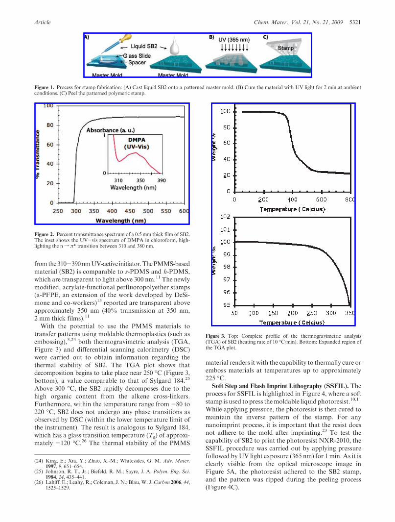
To test submicrometer pattern transfer to the NXR-2010 photoresist under pressure and illumination, thefluorinated SB2-F stamp in Figure 8A was employed asshown in Figure 4 and exposed to UV light through thetop side of the stamp with the transparency of the PMMSmaterial allowing for the curing of the photoresist(365 nm). The process involved applying pressure andillumination of the photoresist for 1 min. After theprinting step, the stamp was peeled with minimal adhe-sion to the substrate. To improve adhesion of the resist tothe substrate, the silicon wafer was pretreated with 3-(tri-methoxysilane)propyloxyacrylate by solution deposition.The patterned stamp in Figure 8A contains features ofposts with a height of approximately 200 nm, width
Figure 4. Process for pattern transfer via SSFIL: (A) Cast/spin coatliquid photoresist onto substratewith orwithout transfer layer. (B)Applypressure and cure with UV light (λ>300 nm using SB2-F). (C) Peel thepatterned polymeric stamp.
Figure 5. Microscope images of the patterns imprinted using two differ-ent stamps (50�). (A) Pristine stamp,without the surface treatment showssignificant adherence. (B) Stampwith the hydrophobic surface treatment.
Figure 6. XPS spectra showing the elemental composition at the surfaceof SB2 (bottom), SB2-OH (center), and SB2-F (top).
(27) Donzel, C.; Geissler, M.; Bernard, A.; Wolf, H.; Michel, B.;Hilborn, J.; Delamarche, E. Adv. Mater. 2001, 13, 1164–1167.
(28) Hui, C. Y.; Jagota, A.; Lin, Y.Y.; Kramer, E. J.Langmuir 2002, 18,1394–1407.
Article Chem. Mater., Vol. 21, No. 21, 2009 5323
approximately 170 nm, and period approximately 250 nm.The SEM image of the printed photoresist in Figure 8Bshows the remarkably well-replicated inverse structure ofthe stamp. Furthermore, the patterning of sub-100 nmpores was accomplished using an SB2-F stamp fabricatedusing a porous aluminum oxide (PAO) master to yieldposts as previously reported.7 Figure 8C shows the SEMimage of the printed photoresist (thickness ca. 70 nm,pore width ca. 55 nm). In both cases there are no apparentimperfections of the posts arising from the applied pres-sure. Another challenge in SFIL is the production of ascum layer with a key feature of PFPE-based systemsbeing the ability to print resists without a scum layer,11,15
that is, a residual layer of resist that prevents the surfaceexposure at the bottom of the pores/wells of the patternedsubstrates. Using the SB2-F stamps, the cross-sectionalSEM images of the printed photoresist clearly shows noobservable scum layer at the bottom of the wells, a pre-eminent feature of PFPE stamps.11,15 Thus, the PMMSmaterials display outstanding characteristics, which showpromise for replacing the hard masters traditionallyemployed in SSFIL.Soft NanoImprint Lithography (SNIL). To test the
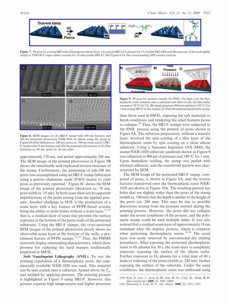
printing capabilities of a thermoplastic resist, the com-mercially available NXR-1020 was used. This materialcan be spin coated onto a substrate, heated above its Tg,and molded by applying pressure. The printing processis highlighted in Figure 9 using SB2-F. However, thisprocess requires high temperatures and higher pressures
than those used in SSFIL, exposing the soft materials toharsh conditions and rendering the relief features proneto collapse.28 Thus, the SB2-F stamps were subjected tothe SNIL process using the pattern of posts shown inFigure 8A. The substrate preparation, without a transferlayer, involved the spin coating of a thin layer of thethermoplastic resist by spin coating on a clean siliconsubstrate. Using a Nanonex Imprinter (NX 2000), thestamp/NXR-1020/substrate sandwich shown in Figure 9was subjected to 400 psi of pressure and 140 �C for 1 min.Upon immediate cooling, the stamp was peeled withminimal adhesion, and the transferred pattern was char-acterized by SEM.The SEM image of the patterned SB2-F stamp, com-
posed of posts, is shown in Figure 8A, and the inversefeatures transferred onto the thermoplastic resist NXR-1020 are shown in Figure 10A. The resulting pattern hasholes that are slightly wider than the posts of the stamp(width ca. 190 nm), but the depth is similar to the height ofthe posts (ca. 200 nm). This may be due to possibledistortions arising from the pressure exerted during theprinting process. However, the posts did not collapseunder the severe conditions of the process, and the poly-meric stamp could be used multiple times. It was alsonoticed that a residual scum layer of approximately 18 nmremained after the imprint process, which is commonwhen patterning thermoplastic resists.29,30 The scumlayer was easily removed by conventional dry etchingprocedures. After exposing the patterned thermoplasticresist to O2 plasma for 30 s, the scum layer is completelyremoved, exposing the surface of the silicon wafer.Further exposure to O2 plasma for a total time of 60 sleads to widening of the pores (width ca. 240 nm), furtherexposing the surface of the substrate. Under the sameconditions, the thermoplastic resist was embossed using
Figure 7. Process for coatingSB2with a fluorinated release layer: (A) exposeSB2 toO2plasma for 15 s (yieldsSB2-OH) and (B) exposure of the hydrophilicstamp to TDFOCS vapor under vacuum for 20 min (yields SB2-F). See Figure 6 for the corresponding XPS surface analysis.
Figure 8. SEM images of (A) SB2-F stamp with 180 nm features and(B) the patterned photoresist NXR-2010 on silicon using the stamp inFigure 8A (film thickness ca. 200 nm, pores ca. 180 nmwide) and (C) SB2-F stampwith 55 nm features and (D) the patterned photoresist on Si (filmthickness ca. 80 nm, pores ca. 60 nm wide).
Figure 9. Process for pattern transfer via SNIL: (A) Spin coat the ther-moplastic resist solution onto a substrate and allow to dry the film undervacuumat 50 �C for 2 h. (B)Apply pressure (400 psi) andheat (140 �C) for1min (using SB2-F as the stamp). (C) Peel the patterned polymeric stamp.
(29) Kim, S.; Lee, J.; Jeon, S.-M.; Lee, H. H.; Char, K.; Sohn, B.-H.Macromolecules 2008, 41, 3401–3404.
(30) Dumond, J.; Low, H. Y. Adv. Mater. 2008, 20, 1291–1297.
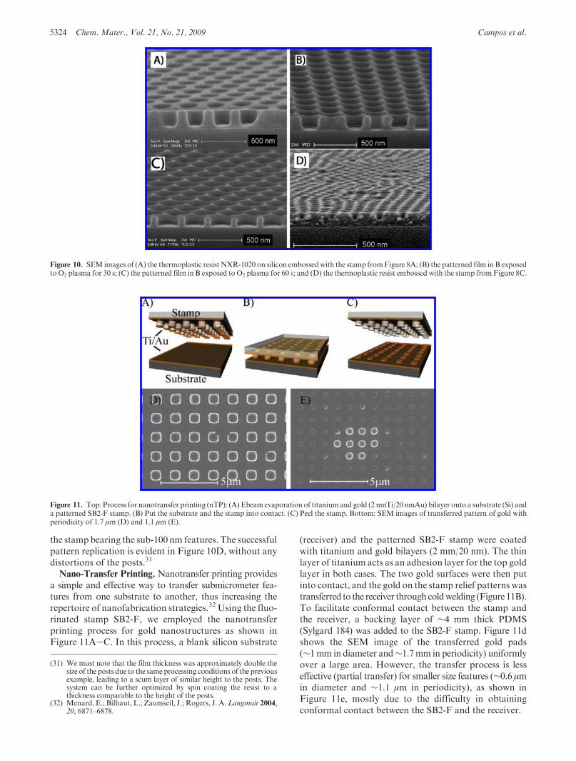
5324 Chem. Mater., Vol. 21, No. 21, 2009 Campos et al.
the stamp bearing the sub-100 nm features. The successfulpattern replication is evident in Figure 10D, without anydistortions of the posts.31
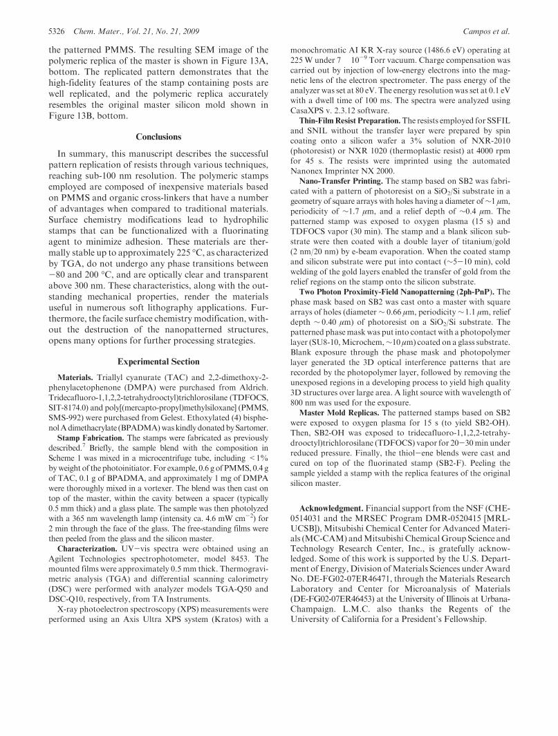
Nano-Transfer Printing. Nanotransfer printing providesa simple and effective way to transfer submicrometer fea-tures from one substrate to another, thus increasing therepertoire of nanofabrication strategies.32 Using the fluo-rinated stamp SB2-F, we employed the nanotransferprinting process for gold nanostructures as shown inFigure 11A-C. In this process, a blank silicon substrate
(receiver) and the patterned SB2-F stamp were coatedwith titanium and gold bilayers (2 mm/20 nm). The thinlayer of titanium acts as an adhesion layer for the top goldlayer in both cases. The two gold surfaces were then putinto contact, and the gold on the stamp relief patterns wastransferred to the receiver throughcoldwelding (Figure11B).To facilitate conformal contact between the stamp andthe receiver, a backing layer of ∼4 mm thick PDMS(Sylgard 184) was added to the SB2-F stamp. Figure 11dshows the SEM image of the transferred gold pads(∼1mm in diameter and∼1.7mm in periodicity) uniformlyover a large area. However, the transfer process is lesseffective (partial transfer) for smaller size features (∼0.6 μmin diameter and ∼1.1 μm in periodicity), as shown inFigure 11e, mostly due to the difficulty in obtainingconformal contact between the SB2-F and the receiver.
Figure 10. SEM images of (A) the thermoplastic resist NXR-1020 on silicon embossedwith the stamp fromFigure 8A; (B) the patterned film in B exposedto O2 plasma for 30 s; (C) the patterned film in B exposed to O2 plasma for 60 s; and (D) the thermoplastic resist embossed with the stamp fromFigure 8C.
Figure 11. Top: Process for nanotransfer printing (nTP): (A) Ebeam evaporation of titaniumand gold (2 nmTi/20 nmAu) bilayer onto a substrate (Si) anda patterned SB2-F stamp. (B) Put the substrate and the stamp into contact. (C) Peel the stamp. Bottom: SEM images of transferred pattern of gold withperiodicity of 1.7 μm (D) and 1.1 μm (E).
(31) We must note that the film thickness was approximately double thesize of the posts due to the same processing conditions of the previousexample, leading to a scum layer of similar height to the posts. Thesystem can be further optimized by spin coating the resist to athickness comparable to the height of the posts.
(32) Menard, E.; Bilhaut, L.; Zaumseil, J.; Rogers, J. A.Langmuir 2004,20, 6871–6878.

Article Chem. Mater., Vol. 21, No. 21, 2009 5325
Proximity-Field Nanopatterning (PnP). The ability ofSB2 to replicate submicrometer features and its transpar-ency in the visible range make it suitable for applicationsin phase mask lithography. Here, we demonstrate the useof SB2 as a phase mask to fabricate a 3D nanostructurethrough two-photon proximity-field nanopatterning(2ph-PnP).33 The fabrication process is shown in Figure 12,top. The phase mask was generated from a photoresistpattern on SiO2/Si substrate that consists of a squarearray of holes with diameter of ∼0.66 μm, periodicityof ∼1.1 μm, and relief depth of ∼0.40 μm. Blank ex-posure with an 800 nm light source through the phasemask generates a 3D optical interference pattern in thephotoactive polymer. The developing process removesthe unexposed regions and creates a well-defined 3D
nanostructure in the photopolymer layer. The SEMimages in Figure 11D,E show the remarkably well-de-fined 3D nanostructure that was fabricated using the SB2stamp.PolymericMasterReplicas.Anadditional advantage of
the surface treatment of the PMMS stamps is the abilityto create replicas of the original master. Taking advan-tage of the polymeric replicas for further stamp fabri-cation minimizes damage to the hard master throughwear-and-tear. Using the fluorinated stamp SB2-F, weemployed the process highlighted in Figure 13, top. Thesame process for stamp fabrication described earlier wasemployed but using the polymeric stamp as the mold.After curing, the new polymeric replica mold composedof SB2 was easily peeled. This process highlights the factthat the surface treatment process left negligible amountsof thiol-ene functional groups capable of covalent at-tachment to the freshly cured SB2. In fact, peeling thereplica was not possible without the surface treatment of
Figure 12. Top:Process for proximity-field patterning (PnP). (A) Spin coat a layerof photopolymer (SU8-10,∼10μm)ontoa glass substrate. (B)Bring thepatterned SB2 phase mask into contact with the photopolymer and expose with a 800 nm light source. (C) Remove the phase mask, develop unexposedregions to yield 3D nanostructure. Bottom: SEM images of the 3D nanostructure in (D) tilted view together with cross-section (inset) and (E) top view.
Figure 13. Top: Replicamolding process with a fluorinated release layer in SB2-F. (B) cast thiol-enemixture on top of SB2-F and photocure. (B) Peel offthe SB2 stamp. Bottom: (A) SEM image of the SB2 replica of the master and (B) the patterned master silicon wafer.
(33) Shir, D. J.; Jeon, S.; Liao, H.; Highland, M.; Cahill, D. G.; Su,M.F.; El-Kady, I. F.; Christodoulou, C.G.; Bogart,G.R.;Hamza,A. V.; Rogers, J. A. J. Phys. Chem. B 2007, 111, 12945–12958.
5326 Chem. Mater., Vol. 21, No. 21, 2009 Campos et al.
the patterned PMMS. The resulting SEM image of thepolymeric replica of the master is shown in Figure 13A,bottom. The replicated pattern demonstrates that thehigh-fidelity features of the stamp containing posts arewell replicated, and the polymeric replica accuratelyresembles the original master silicon mold shown inFigure 13B, bottom.
Conclusions
In summary, this manuscript describes the successfulpattern replication of resists through various techniques,reaching sub-100 nm resolution. The polymeric stampsemployed are composed of inexpensive materials basedon PMMS and organic cross-linkers that have a numberof advantages when compared to traditional materials.Surface chemistry modifications lead to hydrophilicstamps that can be functionalized with a fluorinatingagent to minimize adhesion. These materials are ther-mally stable up to approximately 225 �C, as characterizedby TGA, do not undergo any phase transitions between-80 and 200 �C, and are optically clear and transparentabove 300 nm. These characteristics, along with the out-standing mechanical properties, render the materialsuseful in numerous soft lithography applications. Fur-thermore, the facile surface chemistry modification, with-out the destruction of the nanopatterned structures,opens many options for further processing strategies.
Experimental Section
Materials. Triallyl cyanurate (TAC) and 2,2-dimethoxy-2-
phenylacetophenone (DMPA) were purchased from Aldrich.
Tridecafluoro-1,1,2,2-tetrahydrooctyl)trichlorosilane (TDFOCS,
SIT-8174.0) and poly[(mercapto-propyl)methylsiloxane] (PMMS,
SMS-992) were purchased from Gelest. Ethoxylated (4) bisphe-
nolAdimethacrylate (BPADMA)waskindlydonatedbySartomer.
Stamp Fabrication. The stamps were fabricated as previously
described.7 Briefly, the sample blend with the composition in
Scheme 1 was mixed in a microcentrifuge tube, including <1%
byweight of the photoinitiator. For example, 0.6 g of PMMS, 0.4 g
of TAC, 0.1 g of BPADMA, and approximately 1 mg of DMPA
were thoroughly mixed in a vortexer. The blend was then cast on
top of the master, within the cavity between a spacer (typically
0.5 mm thick) and a glass plate. The sample was then photolyzed
with a 365 nm wavelength lamp (intensity ca. 4.6 mW cm-2) for
2 min through the face of the glass. The free-standing films were
then peeled from the glass and the silicon master.
Characterization. UV-vis spectra were obtained using an
Agilent Technologies spectrophotometer, model 8453. The
mounted films were approximately 0.5 mm thick. Thermogravi-
metric analysis (TGA) and differential scanning calorimetry
(DSC) were performed with analyzer models TGA-Q50 and
DSC-Q10, respectively, from TA Instruments.
X-ray photoelectron spectroscopy (XPS) measurements were
performed using an Axis Ultra XPS system (Kratos) with a
monochromatic AI KR X-ray source (1486.6 eV) operating at
225W under 7� 10-9 Torr vacuum. Charge compensation was
carried out by injection of low-energy electrons into the mag-
netic lens of the electron spectrometer. The pass energy of the
analyzer was set at 80 eV. The energy resolutionwas set at 0.1 eV
with a dwell time of 100 ms. The spectra were analyzed using
CasaXPS v. 2.3.12 software.
Thin-FilmResist Preparation.The resists employed for SSFIL
and SNIL without the transfer layer were prepared by spin
coating onto a silicon wafer a 3% solution of NXR-2010
(photoresist) or NXR 1020 (thermoplastic resist) at 4000 rpm
for 45 s. The resists were imprinted using the automated
Nanonex Imprinter NX 2000.
Nano-Transfer Printing. The stamp based on SB2 was fabri-
cated with a pattern of photoresist on a SiO2/Si substrate in a
geometry of square arrays with holes having a diameter of∼1 μm,
periodicity of ∼1.7 μm, and a relief depth of ∼0.4 μm. The
patterned stamp was exposed to oxygen plasma (15 s) and
TDFOCS vapor (30 min). The stamp and a blank silicon sub-
strate were then coated with a double layer of titanium/gold
(2 nm/20 nm) by e-beam evaporation. When the coated stamp
and silicon substrate were put into contact (∼5-10 min), cold
welding of the gold layers enabled the transfer of gold from the
relief regions on the stamp onto the silicon substrate.
Two Photon Proximity-Field Nanopatterning (2ph-PnP). The
phase mask based on SB2 was cast onto a master with square
arrays of holes (diameter∼ 0.66 μm, periodicity∼1.1 μm, relief
depth ∼ 0.40 μm) of photoresist on a SiO2/Si substrate. The
patterned phasemaskwas put into contact with a photopolymer
layer (SU8-10,Microchem,∼10 μm) coated on a glass substrate.
Blank exposure through the phase mask and photopolymer
layer generated the 3D optical interference patterns that are
recorded by the photopolymer layer, followed by removing the
unexposed regions in a developing process to yield high quality
3D structures over large area. A light source with wavelength of
800 nm was used for the exposure.
Master Mold Replicas. The patterned stamps based on SB2
were exposed to oxygen plasma for 15 s (to yield SB2-OH).
Then, SB2-OH was exposed to tridecafluoro-1,1,2,2-tetrahy-
drooctyl)trichlorosilane (TDFOCS) vapor for 20-30min under
reduced pressure. Finally, the thiol-ene blends were cast and
cured on top of the fluorinated stamp (SB2-F). Peeling the
sample yielded a stamp with the replica features of the original
silicon master.
Acknowledgment. Financial support from the NSF (CHE-0514031 and the MRSEC Program DMR-0520415 [MRL-UCSB]), Mitsubishi Chemical Center for Advanced Materi-als (MC-CAM) andMitsubishi ChemicalGroupScience andTechnology Research Center, Inc., is gratefully acknow-ledged. Some of this work is supported by the U.S. Depart-ment of Energy, Division ofMaterials Sciences under AwardNo. DE-FG02-07ER46471, through theMaterials ResearchLaboratory and Center for Microanalysis of Materials(DE-FG02-07ER46453) at the University of Illinois at Urbana-Champaign. L.M.C. also thanks the Regents of theUniversity of California for a President’s Fellowship.