ansi/scte 199 2013
TRANSCRIPT

ENGINEERING COMMITTEE Interface Practices Subcommittee
AMERICAN NATIONAL STANDARD
ANSI/SCTE 199 2013
Interface Specifications for an RF-Modulated Small
Form Factor Pluggable Optical Receiver Module (SFP-RF-USRx)

i
NOTICE
The Society of Cable Telecommunications Engineers (SCTE) Standards are intended to serve the public interest by providing specifications, test methods and procedures that promote uniformity of product, interchangeability and ultimately the long term reliability of broadband communications facilities. These documents shall not in any way preclude any member or non-member of SCTE from manufacturing or selling products not conforming to such documents, nor shall the existence of such standards preclude their voluntary use by those other than SCTE members, whether used domestically or internationally.
SCTE assumes no obligations or liability whatsoever to any party who may adopt the Standards. Such adopting party assumes all risks associated with adoption of these Standards, and accepts full responsibility for any damage and/or claims arising from the adoption of such Standards.
Attention is called to the possibility that implementation of this standard may require the use of subject matter covered by patent rights. By publication of this standard, no position is taken with respect to the existence or validity of any patent rights in connection therewith. SCTE shall not be responsible for identifying patents for which a license may be required or for conducting inquiries into the legal validity or scope of those patents that are brought to its attention.
Patent holders who believe that they hold patents which are essential to the implementation of this standard have been requested to provide information about those patents and any related licensing terms and conditions. Any such declarations made before or after publication of this document are available on the SCTE web site at http://www.scte.org.
All Rights Reserved
© Society of Cable Telecommunications Engineers, Inc. 2013
140 Philips Road Exton, PA 19341
ii
TABLE OF CONTENTS
1.0 Revision History .................................................................................................... 1
2.0 Scope ..................................................................................................................... 2
3.0 Normative References ........................................................................................... 2
4.0 Informative References ......................................................................................... 3
5.0 Compliance Notation ............................................................................................. 3
6.0 Definitions, Abbreviations, and Acronyms ........................................................... 4
7.0 Management Interface ........................................................................................... 4
7.1 Summary of 2-Wire Communications Requirements ..................................................... 5
7.2 Theory of Operation ........................................................................................................ 6
7.2.1 SFP-RF-USRx Module Boot Up Sequence .................................................................... 6
7.2.2 Host Initialization of the SFP-RF-USRx Module ........................................................... 9
7.2.3 Automatic Gain Control (AGC) in the SFP-RF-USRx Module ................................... 11
7.2.4 SFP-RF-USRx Module Not Ready ............................................................................... 16
7.2.5 Interrupt Conditions from the SFP-RF-USRx Module ................................................. 16
7.3 SFP-RF-USRx Module Memory Map .......................................................................... 18
7.4 Specific Memory Maps ................................................................................................. 20
7.4.1 Volatile and Non-Volatile Field Characteristics ........................................................... 20
7.4.2 Lower Memory Map (Common Table) ........................................................................ 20
7.4.3 Upper Memory Maps .................................................................................................... 25
8.0 Electrical Interface .............................................................................................. 31
8.1 Introduction ................................................................................................................... 31
8.2 Pinout ............................................................................................................................ 32
8.2.1 Pin Definitions .............................................................................................................. 33
8.3 Fixed RF Output ........................................................................................................... 35
iii
8.3.1 Pass Band ...................................................................................................................... 36
8.3.2 RF Power Levels ........................................................................................................... 36
8.3.3 Interface Impedance ...................................................................................................... 38
8.3.4 Output Return Loss ....................................................................................................... 38
8.3.5 Attenuation .................................................................................................................... 38
8.4 DC Power Requirements............................................................................................... 38
8.4.1 Power Noise Output ...................................................................................................... 39
8.4.2 SFP-RF-USRx Module Power Noise Susceptibility..................................................... 40
8.5 Low Speed Electrical Specifications ............................................................................ 40
8.6 Timing Requirements of Control and Status I/O .......................................................... 41
9.0 Mechanical and Board Definition ....................................................................... 41
9.1 Introduction ................................................................................................................... 41
9.2 SFP-RF-USRx Module Mechanical and Labeling Requirements ................................ 42
9.3 Mating of SFP-RF-USRx Module PCB to the Host Electrical Connector ................... 42
9.4 Host Board Layout ........................................................................................................ 43
9.5 Insertion, Extraction and Retention Forces for SFP-RF-USRx Modules ..................... 43
9.6 Color Coding of SFP-RF-USRx Modules .................................................................... 43
9.7 EMI Design Using SFP-RF-USRx Modules ................................................................ 43
9.8 SFP-RF-USRx Module Connector Specifications ........................................................ 43
9.9 SFP-RF-USRx Module Cage Assembly Dimensions ................................................... 43
9.10 SFP-RF-USRx Module Cooling ................................................................................... 44
9.11 Environmental and Thermal ......................................................................................... 44
9.12 Dust Cover .................................................................................................................... 44
9.13 SFP-RF-USRx Module Fiber-Optic End-Face Finish and Connector Geometry ......... 44
Appendix A: Potential RF Output Loss Use Case .................................................................... 44

iv
Appendix B: Acknowledgements ............................................................................................. 46
LIST OF FIGURES
Figure 1 – SFP-RF-USRx Module Boot Sequence......................................................................... 8
Figure 2 – Host SFP-RF-USRx Module Initialization .................................................................... 9
Figure 3 – AGC Control Sequence ............................................................................................... 12
Figure 4 – AGC Functional Flow ................................................................................................. 15
Figure 5 – SFP-RF-USRx Module Memory Layout..................................................................... 19
Figure 6 – SFP-RF-USRx Module Connector Pin Numbers and Names ..................................... 31
Figure 7 – Example SFP-RF-USRx Module Block Diagram ....................................................... 36
Figure 8 – Rx1 and Rx2 Port Layout ............................................................................................ 42
Figure 9 – Example Output Losses ............................................................................................... 45
LIST OF TABLES
Table 1 – Receiver Alarm and Warning Thresholds .................................................................... 21
Table 2 – Latched Alarms and Warnings ..................................................................................... 22
Table 3 – Masking Bits for Alarms and Warnings ....................................................................... 22
Table 4 – A/D Readout Values ..................................................................................................... 23
Table 5 – General Control/Status Bits .......................................................................................... 24
Table 6 – Auxiliary Input Types ................................................................................................... 26
Table 7 – Table 70h Read Only Values ........................................................................................ 28
Table 8 – Table 70h Writable Values ........................................................................................... 29
Table 9 – SFP-RF-USRx Module Electrical Pin Definition ......................................................... 32
Table 10 – Optical Power Ranges, Based on Optical Input Power .............................................. 38
Table 11 – Power per Rail ............................................................................................................ 39

v
Table 12 – Low Speed Control and Sense Signals, Electronic Characteristics ............................ 40
Table 13 – Timing Parameters for SFP-RF-USRx Module Management .................................... 41

1
1.0 REVISION HISTORY Revision Date Description R01 9/26//2012 Initial publication R02 10/8/2012 Updates to the Electrical Interface section from F2F R03 10/26/2012 Updates the Management Interface and Electrical Interface R04 10/30/2012 Updates from the meeting, plus addition of appendix
describing losses R05 11/5/12 Made the updates to the following:
• Section 7.2.2, Number 2 • Table 2, bytes 84 and 85 • Table 3, bytes 84 and 85 • Table 4 updates • Section 8.3.2
R06 11/7/12 Made updates to the following: • Table 2 • Table 3 • Table 4 • Section 8.3 • Section 9.3 • Appendix A
R07 11/13/12 Made the following updates: • Removed redundant fields from Table 70h • Updated descriptions of MOD_DESEL; assert and
de-assert were backwards R08 11/19/12 Made updates to the following:
• Tables 2 and 3 • Added Table 4 • Added Table 5 • Updates to Table 7 • Updated the formula in section 8.3.2 • Added Table 10
R09 11/20/12 Reviewed and accepted changes during the 11/20/12 meeting. General clean up and definitions updates. Open issues still tracked/commented.
R10 11/28/12 Reviewed and accepted changes during the 11/28/12 meeting. This is the proposed final draft.
R11 12/4/12 Additional changes made during final review; changes are tracked
R12 12/11/12 Additional changes made during final review; changes are tracked
R13 12/13/12 Reverted the final sentence of the MOD_DESEL description back to what it was in the MSA.

2
Revision Date Description R14 12/18/12 SCTE candidate
2.0 SCOPE
The integration of optical interfaces into headend equipment offers cost and power savings to MSOs. However, implementing optical interfaces in these devices presents significant technical challenges, since the lack of standardization may result in too many combinations of interfaces to support effectively in a headend device.
Because of this challenge, it is proposed to create a standard that specifies the interfaces between an upstream laser receiver module and its host. The module is based on [XFP MSA], but is in an SFP form factor and will receive RF-modulated optical signals. This optical receiver module could be deployed in headend equipment, such as the Converged Cable Access Platform (CCAP) or HFC optoelectronics products, providing a standardized, interoperable solution. The optical receiver module will function as an upstream receiver for the output of return optical transmitters inside fiber optic nodes.
This standard focuses on the communication, electrical, and mechanical interfaces for the optical receiver module. Requirements held within this standard apply both to the receiver module and its host.
3.0 NORMATIVE REFERENCES
The following documents contain provisions, which, through reference in this text, constitute provisions of this specification. At the time of subcommittee approval, the editions indicated were valid. All standards and specifications are subject to revision, and parties to agreement based on this specification are encouraged to investigate the possibility of applying the most recent editions of the documents listed below.
Reference Description [IEC 61755-3-1] IEC 61755-3-1:2006, ed. 1.0, July 1, 2006, Fibre optic
connector optical interfaces – Part 3-1: Optical interface, 2,5 mm and 1,25 mm diameter cylindrical full zirconia PC ferrule, single mode fibre. IEC Sub-committee 86B
[IEC 61755-3-2] IEC 61755-3-2, ed. 1.0, July 12, 2006, Fibre optic connector optical interfaces - Part 3-2: Optical interface, 2,5 mm and 1,25 mm diameter cylindrical full zirconia ferrules for 8 degrees angled-PC single mode fibres, IEC Sub-committee 86B
[INF-8074] INF-8074i, Revision 1.0, May 12, 2001, Specification for SFP (Small Formfactor Pluggable) Transceiver, SFF Committee, http://www.sffcommittee.com/

3
[FINISH] IEC 61300-3-35, ed. 1.0, November 20, 2009, Fibre optic interconnecting devices and passive components - Basic test and measurement procedures - Part 3-35: Examinations and measurements - Fibre optic connector endface visual and automated inspection, IEC Sub-committee 86B
[SFF-8083] SFF-8083, Revision 2.5, January 19, 2010, 0.8mm Card Edge Connector for 8/10 Gb/s Applications, SFF Committee, http://www.sffcommittee.com/
[SFF-8432] SFF-8432, Revision 5.0, July 16, 2007, Improved Pluggable Formfactor, SFF Committee, http://www.sffcommittee.com/
[SFF-8433] SFF-8433, Revision 0.7, June 5, 2009, Improved Pluggable Formfactor (IPF) for SFP+ Ganged Cages, SFF Committee, http://www.sffcommittee.com/
[XFP MSA] INF-8077i, Revision 4.5, August 31, 2005, 10 Gigabit Small Form Factor Pluggable Module, SFF Committee, http://www.sffcommittee.com/
4.0 INFORMATIVE REFERENCES
The following documents may provide valuable information to the reader but are not required when complying with this specification.
Reference Description [UM10204] UM10204, Version 4.0, February 13 2012, The I2C-Bus
specification and user manual, NXP Semiconductors
5.0 COMPLIANCE NOTATION “SHALL” This word or the adjective “REQUIRED” means that the item is an
absolute requirement of this specification. “SHALL NOT” This phrase means that the item is an absolute prohibition of this
specification. “SHOULD” This word or the adjective “RECOMMENDED” means that there
may exist valid reasons in particular circumstances to ignore this item, but the full implications should be understood and the case carefully weighted before choosing a different course.
“SHOULD NOT” This phrase means that there may exist valid reasons in particular circumstances when the listed behavior is acceptable or even useful, but the full implications should be understood and the case carefully weighed before implementing any behavior described with this label.
“MAY” This word or the adjective “OPTIONAL” means that this item is truly optional. One vendor may choose to include the item because a particular marketplace requires it or because it enhances the product, for example; another vendor may omit the same item.
4
6.0 DEFINITIONS, ABBREVIATIONS, AND ACRONYMS Term Definition AGC Automatic Gain Control APC Angled Physical Contact APD Avalanche Photodiode CCAP Converged Cable Access Platform CDR Clock Data Recovery CLEI Common Language Equipment Identification CMTS Cable Modem Termination System DC Direct Current or Directional Coupler DSA Digital Step Attenuator EEPROM Electrically Erasable Programmable Read-Only Memory EMI Electromagnetic Interference HFC Hybrid Fiber-Coax host The device into which the optical module is integrated. I/O Input/Output I2C Inter-Integrated Circuit, a 2-wire communication interface LOS Loss of Signal NVRAM Non-Volatile Random-Access Memory OMI Optical Modulation Index PD Photodiode R/W Read/Write RF Radio Frequency RFoG RF over Glass RX Receive SCL Serial Clock SDA Serial Data SFP Small Formfactor Pluggable TEC Thermo-Electric Cooler TX Transmit UPC Ultra Physical Contact USRx Upstream Receiver XFP 10 Gigabit Small Form Factor Pluggable; a standard for an optical
transceiver. See [XFP MSA].
7.0 MANAGEMENT INTERFACE
2-Wire Communications (I²C) for the SFP-RF-USRx module are based upon [XFP MSA]. I²C is an implementation of the NXP (formerly Philips) I²C [UM10204] specification with mapped memory address locations (also known as “well-known addresses”) for diagnostics and operations. The SFF Committee specifies the I²C common memory mapping in [XFP MSA] for SFP and XFP, as well as additional physical layer requirements. This specification uses the same well-known memory map locations (addresses) for functions that are the same or substantially similar. Because the

5
SFP-RF-USRx is a dual receiver (and not a transceiver), there is a need for additional and different functions that the SFF specifications do not require.
The SFP-RF-USRx module shall implement the I2C requirements specified in [XFP MSA], except where specified differently in the following sections.
7.1 Summary of 2-Wire Communications Requirements
In [XFP MSA] 2-wire communication requirements are spread across several sections, including section 4.2 and Table 26, section 2.6 and Table 3. The following bullets summarize these requirements; refer to [XFP MSA] for complete details.
• I²C communications may not be available for up to 300 ms after power up or reset
• The MOD_DESEL pin functions as defined in section 4.2 of [XFP MSA]. Note, if the I²C interface bus is not shared, the MOD_DESEL pin may be pulled low permanently.
• There must be at least 20 µs between the STOP signal and the next START signal for a particular module.
• The clock rate can be as high as 400 kHz (I²C fast mode).
• Up to two START signals per command are allowed (the second START is also known as a RESTART signal).
• Only one STOP signal is allowed per command.
• Multiple master systems are not supported.
• Host boards shall accommodate SFP-RF-USRx modules that hold the SCL line low (clock stretching) for up to a maximum of 500 µs during an I²C read or write operation.
• After a write from the host to the module, the module may not respond to further I²C commands for up to 40 ms (typically this would be for writing non-volatile values). The phrase “not respond” means that the device address given immediately after the START signal from the host is not acknowledged by the module.
• I²C packet error checking protocol is optional as defined in the [XFP MSA].

6
7.2 Theory of Operation
Using Chapter 5: Management Interface of [XFP MSA] as reference, the following sections define the operation of the SFP-RF-USRx module I²C interface that is used for serial ID, digital diagnostics and other control/monitoring functions.
7.2.1 SFP-RF-USRx Module Boot Up Sequence
When a SFP-RF-USRx module is plugged in, the host needs to perform a number of initialization steps in a particular order with a particular timing. Some of these involve the SFP-RF-USRx module pins, and some involve I²C communications. As most of these are documented in the [XFP MSA] or are implied by stated dependencies, a reference to the location(s) in that document will accompany each step in the following sequence descriptions.
Before the boot up sequence can be discussed, communications and host requirements need to be understood.
7.2.1.1 I²C Communications Requirements
Once I²C is operational, the host shall adhere to the following timing and pin requirements (see [XFP MSA] section 4.2, Table 26):
• The host shall pull MOD_DESEL low for a minimum of 2 ms before issuing the START signal (Host_select_setup).
• While MOD_DESEL is low, the host shall wait at least 20 µs after the previous STOP signal before issuing a new START signal (tBUF).
If the SFP-RF-USRx module is not sharing the I²C interface bus with other SFP-RF-USRx modules, the MOD_DESEL pin may be left low indefinitely. Otherwise, it shall be pulled high for at least 2 ms before another command is executed on the shared bus (presumably to a different SFP-RF-USRx module).
Write operations may cause the SFP-RF-USRx module to not respond to further I²C signals or messages for up to 40 ms (tWR in section 4.3, Table 27, and section 4.5.7 of [XFP MSA]). The specification does not restrict this to EEPROM writes. This applies for writes from one to four bytes (the limit for a write is four bytes).
7
The SFP-RF-USRx module may perform a clock stretch of up to 500 µs during read or write operations (T_clock_hold, [XFP MSA] section 4.3, Table 27). This is distinct from unresponsiveness after a write operation (tWR).
7.2.1.2 Pin State Prior to SFP-RF-USRx Module Boot Up
Before a SFP-RF-USRx module can begin boot up, the host shall meet the following pin requirements.
The voltages listed for pins 15 (VCC3_DIGITAL) and 16 (VCC5_ANALOG) in Table 9 shall be available.
The value of pin 7 (P_DOWN/RST) should be set to low to allow the SFP-RF-USRx module to run in full power (power level II or III), although a setting of high may be used to limit the SFP-RF-USRx module to low power consumption (≤ 1.0 watts). Refer to section 2.4.7.3, Module Behavior During Power Down and Reset of [XFP MSA] for further details.
Pin 8 (INTERRUPT) shall be pulled high by the host. If an unmasked error, alarm or warning condition is encountered during operation, the SFP-RF-USRx module shall pull this value low.
7.2.1.3 Initial SFP-RF-USRx Module Boot Sequence
Once the SFP-RF-USRx module is inserted, it goes through its initialization sequence, as shown in the following flow chart.

8
Figure 1 – SFP-RF-USRx Module Boot Sequence
This series of actions is described here.
1. The SFP-RF-USRx module shall indicate its presence to the host by grounding pin 6 (MOD_ABS) upon insertion.
2. After 300 ms, SFP-RF-USRx module initialization (aka Reset Complete, described in Table 39 of [XFP MSA]) shall be finished (t_init, [XFP MSA] section 2.6, Table 3).
3. The SFP-RF-USRx module shall assert pin 8 (INTERRUPT ) to low and set corresponding Reset Complete flag ([XFP MSA] section 2.4.7.3, Table 39). Reset Complete can be detected by the host via an INTERRUPT signal (pin 8 pulled low) with a corresponding Reset Complete flag being set.
Note that until the boot sequence is complete, signals on the RF output pins may not be valid and the SFP-RF-USRx module shall not assert the INTERRUPT pin spuriously, as detailed in section 2.4.7.3 of [XFP MSA].
The Reset Complete flag also does not imply that registers are valid; the module sets the Data_Not_Ready flag (from

9
Table 42 in [XFP MSA]) to low to indicate that register contents are valid and can be read. When the module is ready to function, the MOD_NR pin is pulled low.
7.2.2 Host Initialization of the SFP-RF-USRx Module
After the module has pulled MOD_NR low, the host shall initialize the module, including interrupt masks, control, and miscellaneous parameters, as detailed in the following flow chart.
Figure 2 – Host SFP-RF-USRx Module Initialization
This series of actions is described here.
1. The host can set alarm and warning masks for any events of interest. These can be found in Table 40

10
in section 5.11.1 of [XFP MSA] with the exception of those alarms and warnings listed in section 7.4.2, Lower Memory Map (Common Table). By default none of these is masked. In particular, the Reset Complete status bit (and its corresponding INTERRUPT) is not masked. At a minimum, the host should set the masking bits for:
• TX_NR
• Laser Fault
• TX CDR Loss of Lock
• TEC Fault
• Vee5 High
• Vee5 Low
• Vcc2 High
• Vcc2 Low
• APD Supply (if it is not supported)
• Wavelength Unlocked
• TX Bias Low
• TX Power Low
2. The host can clear any existing latched alarms by reading those alarm bits (the alarm bits are listed in Table 39 in section 5.11.1 of [XFP MSA]). As these flags are latched, their initial presence does not necessarily indicate a continuing fault. For example, the presence of the Reset Complete flag upon insertion of the module is not a fault. Among the existing latched alarms that can be reasonably expected are:
• Reset Complete
• Rx1(2) CDR Loss of Lock (if used)

11
3. In Table 70h in upper memory, the host should update the Rx1 Wavelength and Rx2 Wavelength fields. These are volatile fields.
4. In the lower memory table, the host shall set the Rx1 Disable and Rx2 Disable flags to false.
Table 70h is a new table described in section 7.4.3.3 of this document.
7.2.3 Automatic Gain Control (AGC) in the SFP-RF-USRx Module
When Automatic Gain Control (AGC) is enabled, the US-RF-USRx module will monitor the receive power and automatically adjust the module attenuator settings to keep the RF output level constant. The US-RF-USRx should implement AGC. When AGC is supported, the module and the host exchange information to enable AGC and set baseline levels. AGC should not be enabled in RFoG applications.
The control flow for enabling AGC is shown in Figure 3.

12
Figure 3 – AGC Control Sequence
This series of actions by the host and module is described here. Note that in the process flow diagram and the following

13
description, “Rx1(2)” means that the value is updated for both Rx1 and Rx2.
1. If not already set to 0 (zero), the host will set Rx1(2) AGC Control to 0. This disables AGC.
2. The operator will manually adjust the attenuator settings to achieve the desired RF output level. The attenuator level is set by the host writing a value to the Rx1(2) Attenuator Set Pt field.
3. When adjustments are complete, the host will set the value of the AGC Capture Action field to 1. This informs the module that it should capture the incoming current level and the attenuator setting.
4. The module will measure incoming current and write this value to the Rx1(2) Detector Current Ref field. It will also write the value from the Rx1(2) Attenuator Set Pt field to the Rx1(2) Attenuator Ref field.
5. The module updates the value of the AGC Capture Action field to 2. This value informs the host that the capture is complete.
6. The host reads the value of the AGC Capture Action field; when set to 2, the host enables AGC by setting AGC Control to 1.
7. The host then sets the value of AGC Capture Action field back to 0.
7.2.3.1 AGC Functions in the SFP-RF-USRx Module
When Optical AGC is enabled, the SFP-RF-USRx monitors the photodiode (PD) current, compares it to the stored reference value (Rx1(2) Detector Current Ref), and adjusts the internal attenuator to attempt to keep the composite RF output level constant. For every 1 dB change in PD current, the module shall adjust the attenuator by 2 dB. For example, if the DC current decreases by 1.5 dB, then the attenuation shall be decreased by 3 dB.
Note that the RF output level can vary even if the optical input/PD current does not change due to changes in the optical modulation index (OMI). These variations are not mitigated with AGC.

14
Considerations should be taken in the design of the module and AGC control logic to ensure that changes in the attenuator setting do not induce bit errors in the return signals. These could include slew rate of the attenuator, attenuator step size, hysteresis value, and the AGC control loop time.
The logic flow for AGC control in the SFP-RF-USRx module is shown in Figure 4.
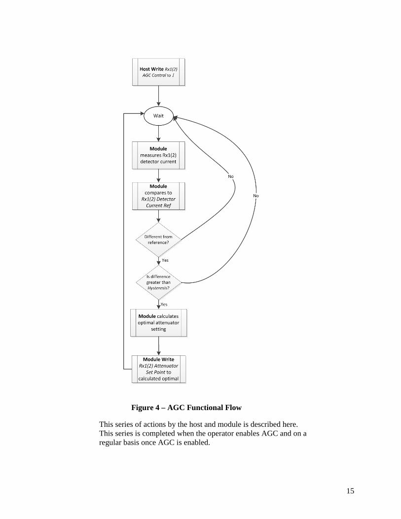
15
Figure 4 – AGC Functional Flow
This series of actions by the host and module is described here. This series is completed when the operator enables AGC and on a regular basis once AGC is enabled.

16
1. This flow is initiated by the host setting the AGC Control field to 1 (enabled).
2. The module waits before moving on to the next step of the flow. Care must be taken not to complete this logic flow too often, as this could cause data errors. Conversely, completing this flow too infrequently could result in errors due to poor attenuation settings.
3. The module measures current at the Rx1(2) detectors. This is the optical input power.
4. The module compares these values to the Rx1(2) values captured in the Rx1(2) Detector Current Ref fields. These measurements were captured while AGC was being initiated.
5. If the difference between the measured current and the reference current is less than or equal to the value set in the Hysteresis field, the module goes back to step 2 and waits to make these measurements and comparisons again.
6. If the difference between the measured current and the reference current is greater than the value set in the Hysteresis field, the module calculates the appropriate attenuator setting: for every 1 dB Optical power change, there will be 2 dB RF power change; this is calculated using the Attenuator Ref and Rx1(2) Detector Current Ref.
7. The module updates the Rx1(2) Attenuator Set Point to match the calculated attenuator setting. The module then goes back to step 2 and waits to make these measurements and comparisons again.
7.2.4 SFP-RF-USRx Module Not Ready
When an SFP-RF-USRx module is removed or a fatal condition is encountered, the MOD_NR pin (pin 2) is pulled high and stays high until the module is ready for operation.
7.2.5 Interrupt Conditions from the SFP-RF-USRx Module
The following section is based on section 5.11 of [XFP MSA]; modifications have been made for this specification.

17
The SFP-RF-USRx module shall implement a real-time hardware INTERRUPT pin (pin 8) to alert the host system to any condition outside normal operating conditions. Interrupt system logic shall be triggered and latched by a set of flags. These include:
• Alarm and warning flags as described in section 5.6, Basic Monitoring Functions of [XFP MSA]. These correspond to monitored quantities going outside factory programmed threshold values.
• Flags corresponding to basic SFP-RF-USRx module status conditions including:
• RX1(2)_NR: Any condition leading to invalid data on the Rx path (one for each receiver)
• RX1(2)_LOS: Rx loss of signal (one for each receiver)
• AGC alarms and warnings (for analog receivers)
• MOD_NR: Module Not Ready (mirroring hardware output pin)
• Reset Complete: Indicates completion of the SFP-RF-USRx Module Reset (as initiated by power up or P_DOWN/RST pin)
The module shall not generate alarms or events defined in [XFP MSA] for any functions that it does not support (for example, transmitter functions).
This specification uses byte 85, bit 0 for a vendor-specific alarm.
Nothing in the SFP-RF-USRx Table 70h is designed to produce an interrupt.
Existence of any of these conditions shall lead to a latched flag. These flags are located in bytes 80 – 87 and are detailed in Table 39 of [XFP MSA]. The presence of any 1 value in bytes 80 – 87 without a corresponding mask bit set to 1 will assert the hardware INTERRUPT output pin (active low). When the INTERRUPT pin alerts the host system to a latched flag condition, the host may query the latched flag bits in bytes 80 – 87. The SFP-RF-USRx module shall clear the latched flags upon the read of the corresponding latched flag bit.

18
Masking bits shall be volatile and startup with all unmasked (masking bits 0).
Hardware INTERRUPT Pin = Logical NOR of all (Latched Flag Bit AND NOT Masking Bit)
The mask bits can be used to prevent continued interruption from ongoing conditions. This specification uses byte 93, bit 0 for the vendor-specific alarm mask.
7.3 SFP-RF-USRx Module Memory Map
The structure of the SFP-RF-USRx module memory map is shown in Figure 4. The SFP-RF-USRx module shall implement the memory map specified in section 5 of [XFP MSA], with the exceptions specified here.
The normal 256 byte I²C address is divided into lower and upper blocks of 128 bytes. The lower block of 128 bytes is always directly available and is intended to be used for diagnostic and control functions that are accessed often. This is the common table; it is accessed if the I²C address is less than 128 without regard to the selected table.
Multiple blocks of memory are available in the upper 128 bytes of the address space. These are individually addressed via a table select byte located in the lower address space (at offset 127). The upper address tables are intended to contain information that is accessed less frequently, such as serial ID, user writable EEPROM, etc. The password must be entered before any upper memory can be accessed. The password entry stays in effect until the module is power cycled.
The I²C address of the SFP-RF-USRx module shall be 1010000Xb (A0h). In order to support access to multiple SFP-RF-USRx modules on the same I²C serial bus, the SFP-RF-USRx pin-out includes a MOD_DESEL or module deselect pin. This pin shall be held low by the host to address a particular SFP-RF-USRx module.
Figure 5 summarizes the memory layout. The major difference from [XFP MSA] is that a new table, 70h, is defined near the end of the range of the vendor-specific tables. Some fields are not supported, as detailed in section 7.4.2.

19
Figure 5 – SFP-RF-USRx Module Memory Layout

20
7.4 Specific Memory Maps
7.4.1 Volatile and Non-Volatile Field Characteristics
7.4.1.1 Non-Volatile Field Resilience
The SFP-RF-USRx module shall meet the [XFP MSA] specification requirement for EEPROM write cycles (at least 50,000 write cycles). If a host were to write to such a field once per minute, then the EEPROM would expire in roughly 35 days. Writing once per hour gives a lifetime of about 5.7 years.
7.4.1.2 Access Rate for Volatile and Read-Only Fields
While there is no maximum rate for these fields, there is an I²C limitation. Therefore, the host should not expect “tight loop” level of control.
7.4.2 Lower Memory Map (Common Table)
The lower 128 bytes of the I²C serial bus address space is used to access a variety of measurements and diagnostic functions, and to implement a set of control functions. The contents of the lower memory map shall conform to the [XFP MSA] I²C specification unless specified otherwise below.
• The following values are not used by the SFP-RF-USRx module. They are not repurposed. The SFP-RF-USRx module shall set all of these values to 0. The host shall ignore all of these bits. These include:
o Line-side Loopback Control
o XFI Loopback Control
o Acceptable BER for FEC system
o Actual BER for FEC system
o FEC Amplitude Adj
o FEC Phase Adj
o Data Rate Control
o Signal Conditioner Control

21
• The value of the Identifier field shall be 0Dh (SFP-RF-USRx) rather than 06h (XFP).
• In bytes 86, 87, 94, and 95, the VCC2 values shall correspond to VCC5_ANALOG and the VCC3 values shall correspond to VCC3_DIGITAL.
• The bytes from the Lower Memory Map of [XFP MSA] listed in Table 1 shall be re-purposed for receiver alarm and warning thresholds. The default value for each of these bytes is vendor-specific.
Table 1 – Receiver Alarm and Warning Thresholds Address Host
Read/ Write
Bytes Name of Field Remarks
26 R/W 2 Rx1 Opt Power High Alarm
Range (0.0000 to 6.5535). Units: mW. Rx1 upper threshold limit to trigger alarm on optical input power.
28 R/W 2 Rx1 Opt Power Low Alarm
Range (0.0000 to 6.5535). Units: mW. Rx1 lower threshold limit to trigger alarm on optical input power.
30 R/W 2 Rx1 Opt Power High Warning
Range (0.0000 to 6.5535). Units: mW. Rx1 upper threshold limit to trigger warning on optical input power.
32 R/W 2 Rx1 Opt Power Low Warning
Range (0.0000 to 6.5535). Units: mW. Rx1 lower threshold limit to trigger warning on optical input power.
34 R/W 2 Rx2 Opt Power High Alarm
Range (0.0000 to 6.5535). Units: mW. Rx2 upper threshold limit to trigger alarm on optical input power.
36 R/W 2 Rx2 Opt Power Low Alarm
Range (0.0000 to 6.5535). Units: mW. Rx2 lower threshold limit to trigger alarm on optical input power.
38 R/W 2 Rx2 Opt Power High Warning
Range (0.0000 to 6.5535). Units: mW. Rx2 upper threshold limit to trigger warning on optical input power.
40 R/W 2 Rx2 Opt Power Low Warning
Range (0.0000 to 6.5535). Units: mW. Rx2 lower threshold limit to trigger warning on optical input power.
• The following bytes and bits from Table 39 of [XFP MSA] shall be re-purposed for latched alarms and warnings, as listed in Table 2:
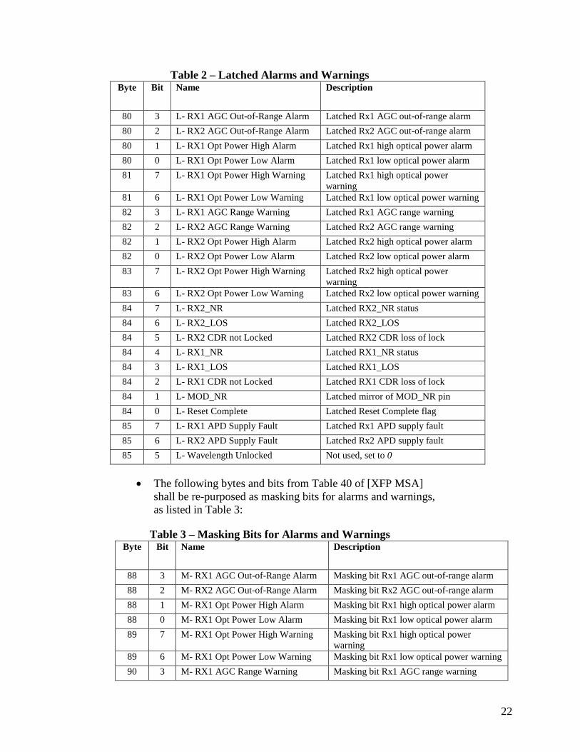
22
Table 2 – Latched Alarms and Warnings Byte Bit Name Description
80 3 L- RX1 AGC Out-of-Range Alarm Latched Rx1 AGC out-of-range alarm 80 2 L- RX2 AGC Out-of-Range Alarm Latched Rx2 AGC out-of-range alarm 80 1 L- RX1 Opt Power High Alarm Latched Rx1 high optical power alarm 80 0 L- RX1 Opt Power Low Alarm Latched Rx1 low optical power alarm 81 7 L- RX1 Opt Power High Warning Latched Rx1 high optical power
warning 81 6 L- RX1 Opt Power Low Warning Latched Rx1 low optical power warning 82 3 L- RX1 AGC Range Warning Latched Rx1 AGC range warning 82 2 L- RX2 AGC Range Warning Latched Rx2 AGC range warning 82 1 L- RX2 Opt Power High Alarm Latched Rx2 high optical power alarm 82 0 L- RX2 Opt Power Low Alarm Latched Rx2 low optical power alarm 83 7 L- RX2 Opt Power High Warning Latched Rx2 high optical power
warning 83 6 L- RX2 Opt Power Low Warning Latched Rx2 low optical power warning 84 7 L- RX2_NR Latched RX2_NR status 84 6 L- RX2_LOS Latched RX2_LOS 84 5 L- RX2 CDR not Locked Latched RX2 CDR loss of lock 84 4 L- RX1_NR Latched RX1_NR status 84 3 L- RX1_LOS Latched RX1_LOS 84 2 L- RX1 CDR not Locked Latched RX1 CDR loss of lock 84 1 L- MOD_NR Latched mirror of MOD_NR pin 84 0 L- Reset Complete Latched Reset Complete flag 85 7 L- RX1 APD Supply Fault Latched Rx1 APD supply fault 85 6 L- RX2 APD Supply Fault Latched Rx2 APD supply fault 85 5 L- Wavelength Unlocked Not used, set to 0
• The following bytes and bits from Table 40 of [XFP MSA] shall be re-purposed as masking bits for alarms and warnings, as listed in Table 3:
Table 3 – Masking Bits for Alarms and Warnings Byte Bit Name Description
88 3 M- RX1 AGC Out-of-Range Alarm Masking bit Rx1 AGC out-of-range alarm 88 2 M- RX2 AGC Out-of-Range Alarm Masking bit Rx2 AGC out-of-range alarm 88 1 M- RX1 Opt Power High Alarm Masking bit Rx1 high optical power alarm 88 0 M- RX1 Opt Power Low Alarm Masking bit Rx1 low optical power alarm 89 7 M- RX1 Opt Power High Warning Masking bit Rx1 high optical power
warning 89 6 M- RX1 Opt Power Low Warning Masking bit Rx1 low optical power warning 90 3 M- RX1 AGC Range Warning Masking bit Rx1 AGC range warning

23
Byte Bit Name Description
90 2 M- RX2 AGC Range Warning Masking bit Rx2 AGC range warning 90 1 M- RX2 Opt Power High Alarm Masking bit Rx2 high optical power alarm 90 0 M- RX2 Opt Power Low Alarm Masking bit Rx2 low optical power alarm 91 7 M- RX2 Opt Power High Warning Masking bit Rx2 high optical power
warning 91 6 M- RX2 Opt Power Low Warning Masking bit Rx2 low optical power warning 92 7 M- RX2_NR Masking bit RX2_NR Status 92 6 M- RX2_LOS Masking bit RX2_LOS 92 5 M- RX2 CDR not Locked Masking bit Rx2 CDR loss of lock 92 4 M- RX1_NR Masking bit RX1_NR status 92 3 M- RX1_LOS Masking bit RX1_LOS 92 2 M- RX1 CDR not Locked Masking bit Rx1 CDR loss of lock 92 1 M- MOD_NR Masking bit MOD_NR 92 0 M- Reset Complete Masking bit Reset Complete flag 93 7 M- RX1 APD Supply Fault Masking bit Rx1 APD supply fault 93 6 M- RX2 APD Supply Fault Masking bit Rx2 APD supply fault 93 5 M- Wavelength Unlocked Not used, set to 0
• The following bytes from Table 41 of [XFP MSA] shall be re-purposed for receiver detector current and optical input power, as listed in Table 4:
Table 4 – A/D Readout Values Bytes Name Description
98-99 A/D readout: Rx1 Detector Current Range (0.0 to 6553.5). Units: µA. Rx1 measured value of detector DC current level. This field is volatile.
100-101 A/D readout: Rx2 Detector Current Range (0.0 to 6553.5). Units: µA. Rx2 measured value of detector DC current level. This field is volatile.
102-103 A/D readout: Rx1 Opt Power Range (0.0000 to 6.5535). Units: mW. Rx1 measured received optical power. Calculated from detector DC current and detector responsivity (which is a function of wavelength). See Note 1. This field is volatile.
104-105 A/D readout: Rx2 Opt Power Range (0.0000 to 6.5535). Units: mW. Rx2 measured received optical power. Calculated from detector DC current and detector responsivity (which is a function of wavelength). See Note 1. This field is volatile.
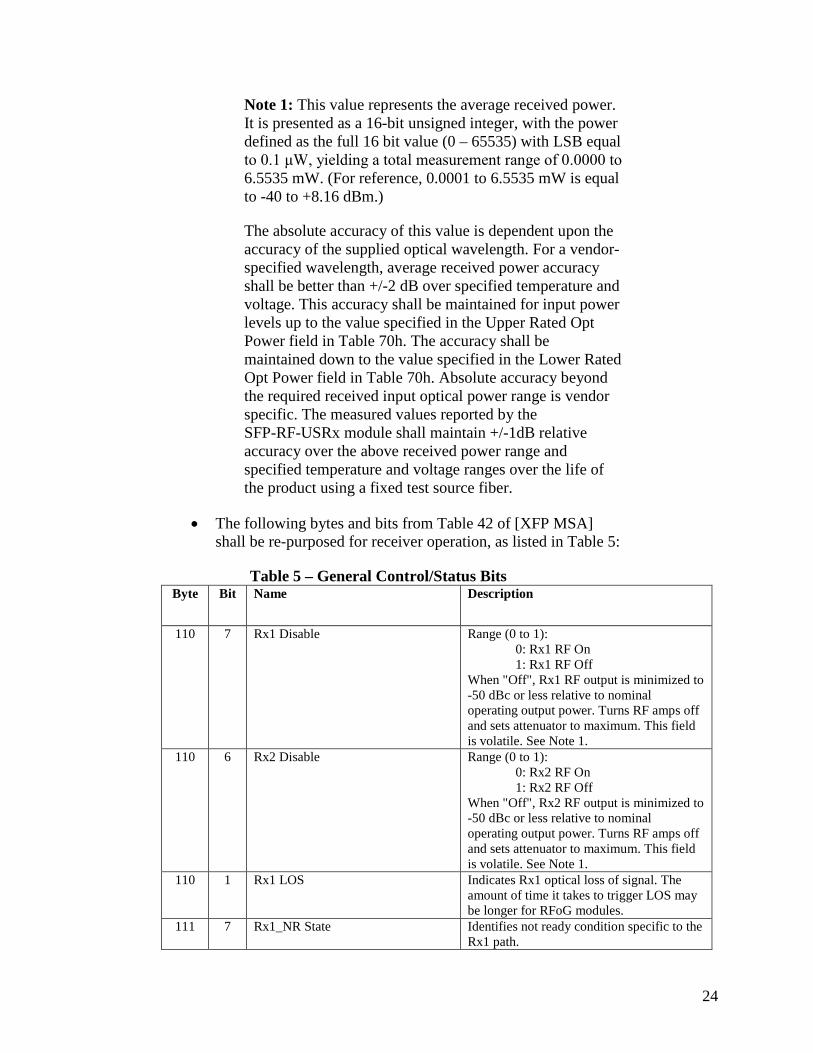
24
Note 1: This value represents the average received power. It is presented as a 16-bit unsigned integer, with the power defined as the full 16 bit value (0 – 65535) with LSB equal to 0.1 μW, yielding a total measurement range of 0.0000 to 6.5535 mW. (For reference, 0.0001 to 6.5535 mW is equal to -40 to +8.16 dBm.)
The absolute accuracy of this value is dependent upon the accuracy of the supplied optical wavelength. For a vendor-specified wavelength, average received power accuracy shall be better than +/-2 dB over specified temperature and voltage. This accuracy shall be maintained for input power levels up to the value specified in the Upper Rated Opt Power field in Table 70h. The accuracy shall be maintained down to the value specified in the Lower Rated Opt Power field in Table 70h. Absolute accuracy beyond the required received input optical power range is vendor specific. The measured values reported by the SFP-RF-USRx module shall maintain +/-1dB relative accuracy over the above received power range and specified temperature and voltage ranges over the life of the product using a fixed test source fiber.
• The following bytes and bits from Table 42 of [XFP MSA] shall be re-purposed for receiver operation, as listed in Table 5:
Table 5 – General Control/Status Bits Byte Bit Name Description
110 7 Rx1 Disable Range (0 to 1): 0: Rx1 RF On 1: Rx1 RF Off
When "Off", Rx1 RF output is minimized to -50 dBc or less relative to nominal operating output power. Turns RF amps off and sets attenuator to maximum. This field is volatile. See Note 1.
110 6 Rx2 Disable Range (0 to 1): 0: Rx2 RF On 1: Rx2 RF Off
When "Off", Rx2 RF output is minimized to -50 dBc or less relative to nominal operating output power. Turns RF amps off and sets attenuator to maximum. This field is volatile. See Note 1.
110 1 Rx1 LOS Indicates Rx1 optical loss of signal. The amount of time it takes to trigger LOS may be longer for RFoG modules.
111 7 Rx1_NR State Identifies not ready condition specific to the Rx1 path.
25
Byte Bit Name Description
111 6 Rx2_LOS Indicates Rx2 optical loss of signal. The amount of time it takes to trigger LOS may be longer for RFoG modules.
111 5 Rx1_CDR not Locked Identifies loss of lock in Rx1, if used. See Note 2.
111 4 Rx2_NR State Identifies not ready condition specific to the Rx2 path.
111 3 Rx2_CDR not locked Identifies loss of lock in Rx2, if used. See Note 2.
Note 1: Disabling a receiver shall not result in the assertion of the MOD_NR pin.
Note 2: In upper memory Table 01h, byte 129, bit 5 indicates whether or not the module uses CDR.
7.4.3 Upper Memory Maps
The upper address space tables are used for less frequently accessed functions such as serial ID, user writable EEPROM, reserved EEPROM and diagnostics and control spaces for future standards definition, as well as Manufacturing ID and security code. These are allocated as follows:
• Table 00h: Reserved for future diagnostic and control functions
• Table 01h: SFP-RF-USRx Serial ID Data and Vendor Specific ID Data
• Table 02h: User writable EEPROM (with optional Common Language Equipment Identification (CLEI))
• Table 70h: SFP-RF-USRx Table
7.4.3.1 SFP-RF-USRx Serial ID Data and Vendor Specific ID Data: Table 01h
The serial ID memory map located in Table 01h in the upper address space is used for read-only identification information, except for the last 32 bytes which are vendor EEPROM. The Identifier field at byte 128 is a duplicate of the Identifier field at byte 0 and should be set to 0Dh for the newly defined value of SFP-RF-USRx.
As with the lower (common) table, transmitter fields are ignored.

26
The contents of the vast majority of the fields shall be as indicated in [XFP MSA] with the following exceptions:
• Identifier is set to 0Dh (same as in lower table) for SFP-RF-USRx
• Connector, specified in Table 48 of [XFP MSA], has the additional available values of:
• 0Ch = LC 8° APC
• 0Dh = SC 8° APC
• 0Eh = PIGTAILED LC 8° APC
• 0Fh = PIGTAILED SC 8° APC
Note that the values in Table 48 are specific to UPC.
• Bit 3 of byte 220 (Table 01h) shall be set to Average Received Power
• In the Auxiliary Input Type (byte 222), nibbles 0111b and 1101b, currently defined as +3.3 V, corresponds to VCC3_DIGITAL. Table 4 defines the Auxiliary Input Type values used by the SFP-RF-USRx module; this table is based on Table 59 of [XFP MSA].
Table 6 – Auxiliary Input Types Value Description of physical device 0000b Auxiliary monitoring not implemented 0001b Rx1 APD Bias Voltage
16-bit value is Voltage in units of 10 mV 0010b Reserved 0011b Reserved 0100b Reserved 0101b Rx2 APD Bias Voltage
16-bit value is Voltage in units of 10 mV 0110b +5V Supply Voltage
Encoded as described in section 5.6 of [XFP MSA] 0111b +VCC3_DIGITAL Supply Voltage
Encoded as described in section 5.6 of [XFP MSA] 1000b Reserved 1001b Rx1 composite RF output power at the RF detector
Signed 16-bit twos complement integer Range of -64.000 to +63.998 dBmV in 1/512 dB steps
1010b +5V Supply Current 16-bit value is current in 100 µA
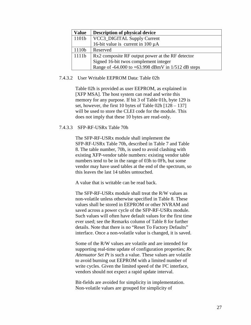
27
Value Description of physical device 1101b VCC3_DIGITAL Supply Current
16-bit value is current in 100 µA 1110b Reserved 1111b Rx2 composite RF output power at the RF detector
Signed 16-bit twos complement integer Range of -64.000 to +63.998 dBmV in 1/512 dB steps
7.4.3.2 User Writable EEPROM Data: Table 02h
Table 02h is provided as user EEPROM, as explained in [XFP MSA]. The host system can read and write this memory for any purpose. If bit 3 of Table 01h, byte 129 is set, however, the first 10 bytes of Table 02h [128 – 137] will be used to store the CLEI code for the module. This does not imply that these 10 bytes are read-only.
7.4.3.3 SFP-RF-USRx Table 70h
The SFP-RF-USRx module shall implement the SFP-RF-USRx Table 70h, described in Table 7 and Table 8. The table number, 70h, is used to avoid clashing with existing XFP-vendor table numbers: existing vendor table numbers tend to be in the range of 03h to 0Fh, but some vendor may have used tables at the end of the spectrum, so this leaves the last 14 tables untouched.
A value that is writable can be read back.
The SFP-RF-USRx module shall treat the R/W values as non-volatile unless otherwise specified in Table 8. These values shall be stored in EEPROM or other NVRAM and saved across a power cycle of the SFP-RF-USRx module. Such values will often have default values for the first time ever used; see the Remarks column of Table 8 for further details. Note that there is no “Reset To Factory Defaults” interface. Once a non-volatile value is changed, it is saved.
Some of the R/W values are volatile and are intended for supporting real-time update of configuration properties; Rx Attenuator Set Pt is such a value. These values are volatile to avoid burning out EEPROM with a limited number of write cycles. Given the limited speed of the I²C interface, vendors should not expect a rapid update interval.
Bit-fields are avoided for simplicity in implementation. Non-volatile values are grouped for simplicity of

28
implementation. The addresses are in the range of 128 to 255 (inclusive). Fields are usually one or two bytes (1B or 2B).
Signed values use the standard 2’s complement encoding. Signed 1-byte ranges are typically -12.8 to +12.7 with 0.1 unit resolution. This may be greater than reasonable for the field, but it gives the greatest possible range of a signed byte. Offsets used in translating the value are used.
For 2-byte fields, the table offset is even to add to simplicity of implementation.
In Table 7 and Table 8, the following values have a specific meaning in the Default column:
V: Vendor-specified MAX: Maximum possible setting.
Table 7 – Table 70h Read Only Values Address Bytes Name of Field Remarks Default
128 1 Rx Options Bit mapped field describing options in this module: Bit 0: Optical AGC Bit 1: RFoG Bit 2-7: Reserved
V
130 2 Lower Frequency Range
Range (0 - 65535). Units: MHz; resolution of 1 MHz. Lower frequency of the operating frequency range of the receivers.
V
132 2 Upper Frequency Range
Range (0 - 65535). Units: MHz; resolution of 1 MHz. Upper frequency of the operating frequency range of the receivers.
V
134 2 Lower Rated Opt Power
Range (0.0000 to 6.5535). Units: mW. Lower limit for rated received optical power.
V
136 2 Upper Rated Opt Power
Range (0.0000 to 6.5535). Units: mW Upper limit for rated received optical power.
V
138 2 Max Rated Attenuator Setting
Range (0.00 to 63.75). Units: dB; step of size of 0.25 dB. Maximum setting possible for the attenuator. The minimum setting possible is assumed to be 0.00.
V
140 2 Rx1 Attenuator Ref Range (0.00 to 63.75). Units: dB; step of size of 0.25 dB. Optical module writes the value of the Rx1 attenuator setting captured during AGC Capture Set function. This field is volatile.
MAX

29
142 2 Rx2 Attenuator Ref Range (0.00 to 63.75). Units: dB; step of size of 0.25 dB. Optical module writes the value of the Rx2 attenuator setting captured during AGC Capture Set function. This field is volatile.
MAX
144 2 Rx1 Detector Current Ref
Range (0.0 to 6553.5). Units: µA Value of the Rx1 photodetector DC current level captured during AGC Capture Set function. This field is volatile.
0.0
146 2 Rx2 Detector Current Ref
Range (0.0 to 6553.5). Units: µA Value of the Rx2 photodetector DC current level captured during AGC Capture Set function. This field is volatile.
0.0
Table 8 – Table 70h Writable Values Address Bytes Name of Field Remarks Default
180 2 Rx1 Attenuator Set Pt
Range (0.00 to 63.75). Units: dB; step of size of 0.25 dB. Host’s ability to write to this field is disabled if the Receiver AGC Control is Enabled.
MAX
182 2 Rx2 Attenuator Set Pt
Range (0.00 to 63.75). Units in dB; step of size of 0.25 dB. Host’s ability to write to this field is disabled if the Receiver AGC Control is Enabled.
MAX
184 1 Rx1 Wavelength Range (0 to 255): 27 (1271 nm) 29 (1291 nm) 31 (1311 nm) 33 (1331 nm) 35 (1351 nm) 37 (1371 nm) 39 (1391 nm) 41 (1411 nm) 43 (1431 nm) 45 (1451 nm) 47 (1471 nm) 49 (1491 nm) 51 (1511 nm) 53 (1531 nm) 55 (1551 nm) 57 (1571 nm) 59 (1591 nm) 61 (1611 nm)
See Note 1. This field is volatile.
31
185 1 Rx2 Wavelength Range (0 to 255): 27 (1271 nm) 29 (1291 nm) 31 (1311 nm) 33 (1331 nm) 35 (1351 nm) 37 (1371 nm) 39 (1391 nm) 41 (1411 nm)
31

30
Address Bytes Name of Field Remarks Default 43 (1431 nm) 45 (1451 nm) 47 (1471 nm) 49 (1491 nm) 51 (1511 nm) 53 (1531 nm) 55 (1551 nm) 57 (1571 nm) 59 (1591 nm) 61 (1611 nm)
See Note 1. This field is volatile. 186 1 Rx1 AGC Control Range (0 to 1):
0: Rx1 AGC Disabled 1: Rx1 AGC Enabled
When enabled, the Rx1 portion of the optical module adjusts Rx1 Attenuator Set Pt by comparing detector current to Rx1 Detector Current Ref. When disabled, the host can adjust Rx1 Attenuator Set Pt directly. This field is volatile.
0
187 1 Rx2 AGC Control Range (0 to 1): 0: Rx2 AGC Disabled 1: Rx2 AGC Enabled
When enabled, the Rx1 portion of the optical module adjusts Rx2 Attenuator Set Pt by comparing detector current to Rx2 Detector Current Ref. When disabled, the host can adjust Rx2 Attenuator Set Pt directly. This field is volatile.
0
188 1 Rx1 AGC Capture Action
Range (0 to 2): 0: Idle 1: Capture Start 2: Capture Complete
Host writes 1 to signal Rx1 portion of the optical module to capture current IDC and Attenuator baseline setting. Once captured, optical module writes 2 (Capture Complete). Host can choose to write register back to 0 (Idle). This field is volatile.
0
189 1 Rx2 AGC Capture Action
Range (0 to 2): 0: Idle 1: Capture Start 2: Capture Complete
Host writes 1 to signal Rx2 portion of the optical module to capture current IDC and Attenuator baseline setting. Once captured, optical module writes 2 (Capture Complete). Host can choose to write register back to 0 (Idle). This field is volatile.
0

31
Address Bytes Name of Field Remarks Default 190 2 Hysteresis Range (0.00 to 63.75).
Units: dB This value sets the threshold that must be crossed before attenuation settings are changed via AGC. This is the difference between the desired optical power and the detected optical power. See section 7.2.3.1 for an explanation of how this value is used.
V
Note 1: This value represents the wavelength of the optical input signal into the receiver from the corresponding return-path transmitter. The host module writes this information because the SFP-RF-USRX does not have the capability to detect wavelength. The wavelength is required by SFP-RF-USRX to select the detector responsivity value from an internal lookup table to use for optical input power calculation. The responsivity of the detector changes based on wavelength.
8.0 ELECTRICAL INTERFACE
8.1 Introduction
The Optical Receiver Module electrical interface is based on the electrical interface defined for the SFP module in [INF-8074]. The electrical interface of the Optical Receiver Module is the shown in Figure 6.
20
19
18
17
16
15
14
13
12
11
1
2
3
4
5
6
7
8
9
10
GND_ANALOG
GND_ANALOG
RF_OUT_2
GND_ANALOG
GND_ANALOG
VCC5_ANALOG
VCC3_DIGITAL
RF_OUT_1
GND_ANALOG
GND_DIGITAL
GND_ANALOG
SDA
MOD_NR
P_DOWN/RST
Reserved
SCL
MOD_ABS
INTERRUPT
MOD_DESEL
GND_DIGITAL
Top of Board Bottom of Board (as viewed through top of board)
Figure 6 – SFP-RF-USRx Module Connector Pin Numbers and Names

32
8.2 Pinout
The SFP-RF-USRx module and host shall conform to the electrical pin definitions specified in Table 9 and the subsections within section 8.2.1.
Table 9 – SFP-RF-USRx Module Electrical Pin Definition Pin Logic Pin Name Function Plug
Seq. Note
1 GND_ANALOG Module analog ground 1 1 2 LVTTL-O MOD_NR Module not ready:
Indicates module operational fault
3 2
3 Reserved 3 4 LVTTL-I/O SDA I2C serial interface data 3 2 5 LVTTL-I/O SCL I2C serial interface clock 3 2 6 LVTTL-O MOD_ABS Indicates module is not
present. Grounded in the module.
3 2
7 LVTTL-I P_DOWN/RST Power down; When high, requires the module to limit power consumption to 1.0 W or below. The I2C serial interface shall be functional in the low power mode. Reset; The falling edge initiates a complete reset of the module, including the I2C serial interface. Equivalent to a power cycle.
3 3
8 LVTTL-O INTERRUPT Indicates presence of an important condition which can be read over the I2C serial interface.
3 2
9 LVTTL-I MOD_DESEL Module deselect; when held low, allows the module to respond to the I2C serial interface.
1 3
10 GND_DIGITAL Module digital ground 1 1 11 GND_DIGITAL Module digital ground 1 1 12 GND_ANALOG Module analog ground 1 1 13 RF_OUT_1 RF output for receiver 1 3 14 GND_ANALOG Module analog ground 1 1

33
Pin Logic Pin Name Function Plug Seq.
Note
15 VCC3_DIGITAL +3.3 V digital power supply
2
16 VCC5_ANALOG +5.0 V analog power supply
2
17 GND_ANALOG Module analog ground 1 1 18 GND_ANALOG Module analog ground 1 1 19 RF_OUT_2 RF output for receiver 2 3 20 GND_ANALOG Module analog ground 1 1 1. Module ground pins shall be isolated from the module case and chassis ground within the module. 2. Shall be pulled up with 4.7 kΩ to 10 kΩ to a voltage between 3.15 V and 3.45 V on the host board. 3. Shall be pulled up with 47 kΩ to 100 kΩ to a voltage between 3.15 V and 3.45 V in the module.
8.2.1 Pin Definitions
8.2.1.1 GND_ANALOG
GND_ANALOG is an internal ground within the module and is the return for the VCC5_ANALOG voltage rail. It is isolated from the module case and chassis ground, as well as the GND_DIGITAL.
8.2.1.2 MOD_NR
The MOD_NR is an output pin that when high, indicates that the module is not able to communicate with the host; for example, the I2C is not functioning.
Other conditions deemed valuable to the detection of fault may be added to the MOD_NR. The MOD_NR output pin is an open collector and must be pulled to Host_Vcc on the host board.
When the receiver module is ready for operation, it shall indicate this by pulling MOD_NR to low. Note that even if the pin is pulled low, faults may exist and can be read from the alarm and warning registers.
8.2.1.3 Reserved
The reserved pins were previously assigned by the SFP MSA and are not required here. They are reserved for future use.

34
8.2.1.4 SCL
The SCL (Serial Clock) pin is bidirectional and is used to positively edge clock data into the module and negative clock data out of each device. The SCL line may be pulled low by a module during clock stretching.
Note: Host devices should filter this pin to prevent interference between it and the RF output.
8.2.1.5 SDA
The SDA (Serial Data) pin is bi-directional for serial data transfer. This pin is open-drain or open-collector driven and may be wire-ORed with any number of open-drain or open collector devices.
Note: Host devices should filter this pin to prevent interference between it and the RF output.
8.2.1.6 MOD_ABS
MOD_ABS is pulled up to Host_Vcc on the host board and grounded in the module to indicate that the module is present. MOD_ABS goes high when the module is physically absent from a host slot.
8.2.1.7 P_DOWN/RST
This is a multifunction pin for module Power Down and Reset. The P_DOWN/RST pin shall be pulled up to +3.3 V in the module.
8.2.1.8 INTERRUPT
INTERRUPT is an output pin. When low, indicates possible module operational fault or a status critical to the host system. The INTERRUPT pin is an open collector output and must be pulled up to Host_Vcc on the host board.
8.2.1.9 MOD_DESEL
The MOD_DESEL is an input pin. When pulled low by the host, the module responds to I2C serial communication commands. The MOD_DESEL pin allows the use of multiple modules on a single I2C interface bus. When the MOD_DESEL pin is high, the module shall not respond to

35
or acknowledge any I2C interface communication from the host. The MOD_DESEL pin shall be pulled to 3.3 V in the module.
In order to avoid conflicts, the host system shall not attempt I2C communications within the MOD_DESEL Host_select_setup time after any modules are deselected. Similarly, the host shall wait at least for the period of the MOD_DESEL Host_select_setup time before communicating with the newly selected module. The assertion and de-assertion periods of different modules may overlap as long as the above timing requirements are met.
8.2.1.10 GND_DIGITAL
GND_DIGITAL is an internal ground within the module and is the return for the VCC3_DIGITAL pin. It is isolated from the module case, chassis ground, and GND_ANALOG.
8.2.1.11 RF_OUT_1
The RF_OUT_1 pin is a nominal 75-Ohm, single-ended RF output pin for receiver 1 in the module.
8.2.1.12 VCC3_DIGITAL
VCC3_DIGITAL is +3.3 VDC pin. See section 8.4, DC Power Requirements for input requirements and pin usage.
8.2.1.13 VCC5_ANALOG
VCC5_ANALOG is a +5.0 VDC pin. See section 8.4, DC Power Requirements for input requirements and pin usage.
8.2.1.14 RF_OUT_2
The RF_OUT_2 pin is a nominal 75-Ohm, single-ended RF output pin for receiver 2 in the module.
8.3 Fixed RF Output
The following figure presents a high-level example of the SFP-RF-USRx module wiring and inputs/outputs. Note that not all pins are represented.
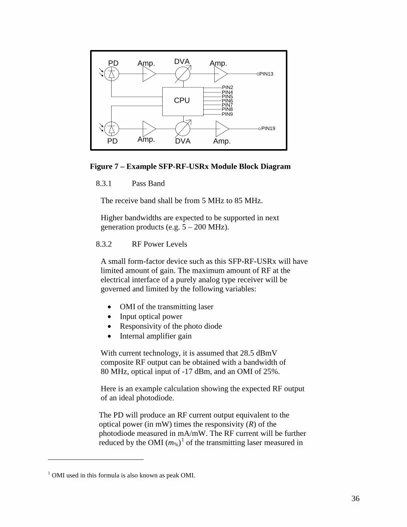
36
PD
PD
Amp.
Amp.
Amp.
Amp.
DVA
DVA
CPU
PIN13
PIN19
PIN2PIN4PIN5PIN6PIN7PIN8PIN9
Figure 7 – Example SFP-RF-USRx Module Block Diagram
8.3.1 Pass Band
The receive band shall be from 5 MHz to 85 MHz.
Higher bandwidths are expected to be supported in next generation products (e.g. 5 – 200 MHz).
8.3.2 RF Power Levels
A small form-factor device such as this SFP-RF-USRx will have limited amount of gain. The maximum amount of RF at the electrical interface of a purely analog type receiver will be governed and limited by the following variables:
• OMI of the transmitting laser • Input optical power • Responsivity of the photo diode • Internal amplifier gain
With current technology, it is assumed that 28.5 dBmV composite RF output can be obtained with a bandwidth of 80 MHz, optical input of -17 dBm, and an OMI of 25%.
Here is an example calculation showing the expected RF output of an ideal photodiode.
The PD will produce an RF current output equivalent to the optical power (in mW) times the responsivity (R) of the photodiode measured in mA/mW. The RF current will be further reduced by the OMI (m%)1 of the transmitting laser measured in
1 OMI used in this formula is also known as peak OMI.

37
percent. All these terms multiplied by the nominal load impedance (Z) and finally divided by √2 to get the rms value will produce the voltage across the load in mV. This voltage can then be converted to dBmV as shown below.
𝑃ℎ𝑜𝑡𝑜𝑑𝑖𝑜𝑑𝑒_𝑅𝐹_𝑂𝑢𝑡(𝑑𝐵𝑚𝑉) = 20 ∙ log10(10𝑃𝑑𝐵𝑚/ 10 ∙ 𝑚% ∙ 𝑅 ∙ 𝑍
√2)
Example:
𝑃𝑑𝐵𝑚 = −17 𝑑𝐵𝑚, 𝑚% = 25%, 𝑅 = 0.95𝑚𝐴𝑚𝑊
, 𝑍 = 75 Ω
20 ∙ log10(10−17 10 ∙ 0.25 ∙ 0.95 ∙ 75
√2)
≈ −12 𝑑𝐵𝑚𝑉
The above power level is the composite power level across an assumed bandwidth of 80 MHz out of the photodiode.
Converted to dBmV/Hz, the signal level ≈ −91 𝑑𝐵𝑚𝑉/𝐻𝑧.
Converted to a 6.4 MHz bandwidth, the signal level out of the photodiode is expected to be ≈ −23 𝑑𝐵𝑚𝑉.
You can see from the above calculations that a net internal gain of 28.5 − (−12) = 40.5 dB still needs to be applied in the SFP-RF-USRx module. This net gain does not include the insertion loss of digital step attenuators (DSA) Z matching, etc.
Also, keep in mind that this module needs to support dual channels and will be space and power limited.
The optical receiver module shall provide a minimum composite output power of 28.5 dBmV within the module’s specified optical input power range and a composite OMI of 25%.
Different types of modules could support different input optical power ranges. It is expected that optical input power will range from -17 dBm to 0 dBm. For RFoG modules, the optical input power could be less than -17 dBm.
The module shall support a frequency response flatness of not worse than +/- 1 dB across the entire pass band.
38
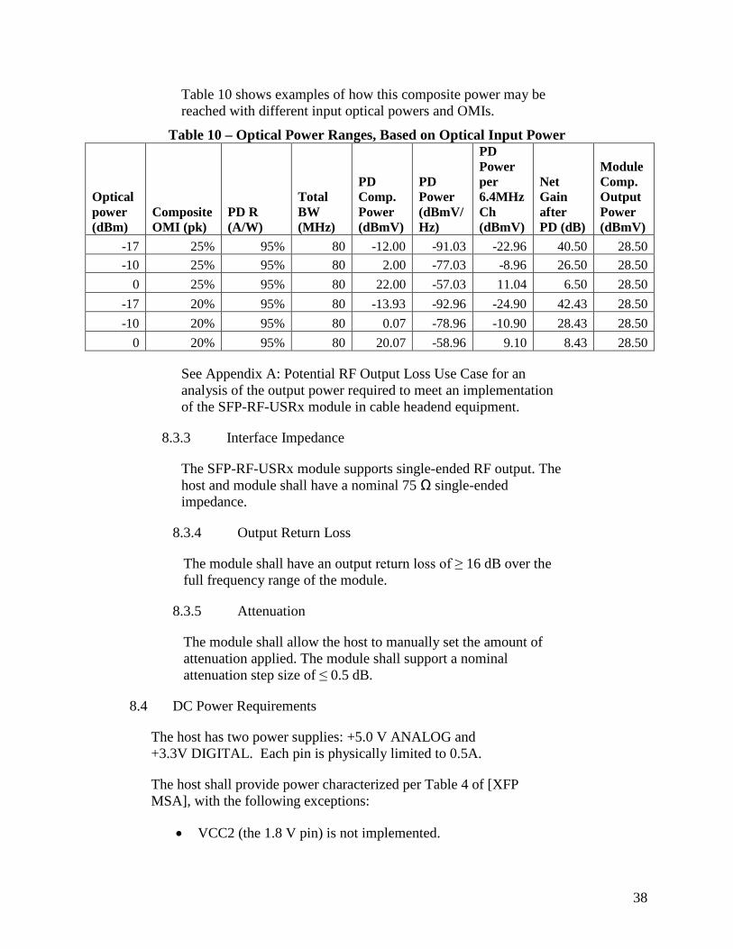
Table 10 shows examples of how this composite power may be reached with different input optical powers and OMIs.
Table 10 – Optical Power Ranges, Based on Optical Input Power
Optical power (dBm)
Composite OMI (pk)
PD R (A/W)
Total BW (MHz)
PD Comp. Power (dBmV)
PD Power (dBmV/Hz)
PD Power per 6.4MHz Ch (dBmV)
Net Gain after PD (dB)
Module Comp. Output Power (dBmV)
-17 25% 95% 80 -12.00 -91.03 -22.96 40.50 28.50 -10 25% 95% 80 2.00 -77.03 -8.96 26.50 28.50
0 25% 95% 80 22.00 -57.03 11.04 6.50 28.50 -17 20% 95% 80 -13.93 -92.96 -24.90 42.43 28.50 -10 20% 95% 80 0.07 -78.96 -10.90 28.43 28.50
0 20% 95% 80 20.07 -58.96 9.10 8.43 28.50
See Appendix A: Potential RF Output Loss Use Case for an analysis of the output power required to meet an implementation of the SFP-RF-USRx module in cable headend equipment.
8.3.3 Interface Impedance
The SFP-RF-USRx module supports single-ended RF output. The host and module shall have a nominal 75 Ω single-ended impedance.
8.3.4 Output Return Loss
The module shall have an output return loss of ≥ 16 dB over the full frequency range of the module.
8.3.5 Attenuation
The module shall allow the host to manually set the amount of attenuation applied. The module shall support a nominal attenuation step size of ≤ 0.5 dB.
8.4 DC Power Requirements
The host has two power supplies: +5.0 V ANALOG and +3.3V DIGITAL. Each pin is physically limited to 0.5A.
The host shall provide power characterized per Table 4 of [XFP MSA], with the following exceptions:
• VCC2 (the 1.8 V pin) is not implemented.

39
• VCC3 applies to the VCC3_DIGITAL pin.
• The Maximum Current Inrush shall be limited to 0.5 A for each VCC5_ANALOG and VCC3_DIGITAL pin.
• Where specified differently in Table 11.
Table 11 – Power per Rail
Rail Voltage
Max Current
Required
Resulting Power per
Rail
Ripple < 100 kHz (mV peak-to-peak)
Ripple > 100 kHz (mV peak-to-peak) Pin
VCC3_DIGITAL +3.3 V 0.45 A1 1.5 W 50 100 15 VCC5_ANALOG +5.0 V 0.40 A 2.0 W 10 30 16 1 0.5A maximum per pin
SFP-RF-USRx module maximum power consumption shall meet one of the following power classes:
• Power Level I modules: ≤ 1.0 W
• Power Level II modules: ≤ 1.5 W
• Power Level III modules: > 1.5 W
8.4.1 Power Noise Output
To limit wide band noise power, the host system and module shall each meet a maximum peak-peak noise, as specified in Table 11 – Power per Rail.
The SFP-RF-USRx receiver port on a host board is tested with a resistive load in place of the SFP-RF-USRx module, each voltage rail at maximum current supported by the host. Voltage is measured at the module side of the SFP-RF-USRx receiver connector. The test is performed with all other portions of the host board/system active. Hosts with multiple SFP-RF-USRx modules will test ports one at a time, with active SFP-RF-USRx receiver modules in all the remaining ports.
The SFP-RF-USRx module is tested with a high-quality power supply connected through the sample filter. Voltage is measured at the host side of the SFP-RF-USRx receiver connector, between the sample host filter network and the SFP-RF-USRx module. The SFP-RF-USRx module shall pass this test in all operating modes. This test ensures the module will not couple excessive noise from inside the module back onto the host board.

40
8.4.2 SFP-RF-USRx Module Power Noise Susceptibility
An SFP-RF-USRx module shall meet all electrical requirements and remain fully operational in the presence of noise on all voltage inputs. The recommended susceptibility test is to sweep a sinusoidal waveform on each voltage input, with peak amplitude as described in Table 11. It is also desirable for a module and host to each tolerate a degree of random or semi-random noise on all voltage pins simultaneously, but the characteristics of this noise are beyond the scope of this document.
8.5 Low Speed Electrical Specifications
The following section is based on section 2.5 of [XFP MSA] and is presented here with modifications.
Low speed signaling is based on Low Voltage TTL (LVTTL) operating at VCC3_DIGITAL at a nominal supply of (3.3 V ±5%). Hosts shall use a pull-up resistor connected to a host_Vcc of +3.3 V (3.15 V to 3.45 V) on the I2C interface SCL (clock), SDA (Data), and all low speed status outputs.
The SFP-RF-USRx module low speed electrical specifications shall conform to those listed in Table 12. This specification ensures compatibility between host bus masters and SFP-RF-USRx SCL/SDA lines and compatibility with I2C.
Table 12 – Low Speed Control and Sense Signals, Electronic Characteristics
Parameter Symbol Min. Max. Unit Conditions
INTERRUPT, MOD_NR
VOL 0.0 0.4 V Rpullup pulled to host_Vcc, measured at host side of connector. IOL(max) = 3 mA
VOH host_Vcc -0.5 host_Vcc +0.3 V Rpullup pulled to host_Vcc, measured at host side of connector.
MOD_DESEL, P_DOWN/RST
VIL -0.3 0.8 V Rpullup pulled to VCC3_DIGITAL, measured at SFP-RF-USRx side of connector. IIL(max) = -10 µA
VIH 2.0 VCC3_DIGITAL + 0.3 V Rpullup pulled to VCC3_DIGITAL, measured at SFP-RF-USRx side of connector. IIH(max) = 10 µA
SCL and SDA
VOL 0.0 0.4 V Rpullup1 pulled to host_Vcc, measured at host side of connector. IOL(max) = 3 mA
VOH host_Vcc - 0.5 host_Vcc + 0.3 V Rpullup1 pulled to host_Vcc, measured at host side of connector.
41
Parameter Symbol Min. Max. Unit Conditions
SCL and SDA
VIL -0.3 VCC3_DIGITAL *0.3 V Rpullup1 pulled to Host_VCC, measured at SFP-RF-USRx side of connector. IIL(max) = -10 µA
VIH VCC3_DIGITAL *0.7 VCC3_DIGITAL + 0.5 V Rpullup1 pulled to Host_VCC, measured at SFP-RF-USRx side of connector. IIH(max) = 10 µA
Leakage Current
Il -10 10 μA
Capacitance for SCL and SDA I/O Pin
Ci 14 pF 10 pF for SFP-RF-USRx IC I/O pin, 4 pF for SFP-RF-USRx PCB trace
Total bus capacitive load for SCL and for SDA
Cb
100 pF At 400 kHz, 3.0 kΩ Rp, max At 100 kHz, 8.0 kΩ Rp, max
400 pF At 400 kHz, 0.80 kΩ Rp, max At 100 kHz, 2.0 kΩ Rp, max
1. For combinations of Rpullup (Rp), bus capacitance and speed, see Figures 39 and 44 of [UM10204]. Rise and fall time measurement levels are defined in the XFP management interface ac electrical specifications. Active bus termination may be used by the host in place of a pullup resistor, as described in [UM10204].
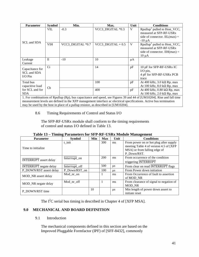
8.6 Timing Requirements of Control and Status I/O
The SFP-RF-USRx module shall conform to the timing requirements of control and status I/O defined in Table 13.
Table 13 – Timing Parameters for SFP-RF-USRx Module Management Parameter Symbol Min Max Unit Conditions
Time to initialize
t_init 300 ms From power on or hot plug after supply meeting Table 4 of version 4.5 of [XFP MSA] or from falling edge of P_Down/RST.
INTERRUPT assert delay Interrupt_on 200 ms From occurrence of the condition triggering INTERRUPT
INTERRUPT negate delay Interrupt_off 500 μs From clear on read INTERRUPT flags P_DOWN/RST assert delay P_Down/RST_on 100 μs From Power down initiation
MOD_NR assert delay Mod_nr_on 1 ms From Occurrence of fault to assertion of MOD_NR
MOD_NR negate delay Mod_nr_off 1 ms From clearance of signal to negation of MOD_NR
P_DOWN/RST time 10 μs Min length of power down assert to initiate reset
The I2C serial bus timing is described in Chapter 4 of [XFP MSA].
9.0 MECHANICAL AND BOARD DEFINITION
9.1 Introduction
The mechanical components defined in this section are based on the Improved Pluggable Formfactor (IPF) of [SFF-8432], commonly
42
known as SFP+. The module and connector dimensions are constant for all applications, while the bezel, cage assembly, and EMI gasket can be designed and/or adjusted for the individual application.
9.2 SFP-RF-USRx Module Mechanical and Labeling Requirements
The SFP-RF-USRx module shall comply with the mechanical and labeling requirements of section 4 of [SFF-8432]. This includes the package dimensions, latch post, retention and extraction features, and durability.
Although pinout differences exist between the MSA SFP/SFP+ and SFP-RF-USRx modules, no mechanical keying is being provided to prevent a module to be inserted into an incompatible host. Permanent damage might occur to either or both the module and host if an MSA compliant digital SFP or SFP+ module is plugged into an SFP-RF-USRx host socket or if an SFP-RF-USRx module is plugged into an MSA compliant SFP or SFP+ host socket.
The SFP-RF-USRx module package shall consist of dual optical receiver ports.
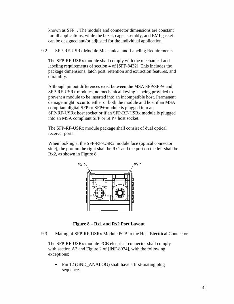
When looking at the SFP-RF-USRx module face (optical connector side), the port on the right shall be Rx1 and the port on the left shall be Rx2, as shown in Figure 8.
Figure 8 – Rx1 and Rx2 Port Layout
9.3 Mating of SFP-RF-USRx Module PCB to the Host Electrical Connector
The SFP-RF-USRx module PCB electrical connector shall comply with section A2 and Figure 2 of [INF-8074], with the following exceptions:
• Pin 12 (GND_ANALOG) shall have a first-mating plug sequence.
43
• Pin 18 (GND_ANALOG) shall have a first-mating plug sequence.
9.4 Host Board Layout
The SFP-RF-USRx module host board layout shall comply with section A2 and Figures 4A and 4B of [INF-8074]. [SFF-8433] shall be used for ganged cages.
9.5 Insertion, Extraction and Retention Forces for SFP-RF-USRx Modules
The SFP-RF-USRx module insertion, extraction, and retention forces shall comply with section 4.2 and Table 4-1 of [SFF-8432].
9.6 Color Coding of SFP-RF-USRx Modules
The SFP-RF-USRx module shall be color coded on the latch, bale, or similar locking mechanism to identify it as a receiver module, as follows:
• Pink for analog receiver
• Pink with black stripes for digital receiver
The color coding for the finish type of the SFP-RF-USRx module shall be color coded on the front face as follows:
• Blue for UPC
• Green for APC
9.7 EMI Design Using SFP-RF-USRx Modules
The host bezel and EMI gasket for the SFP-RF-USRx module shall be consistent with the recommendations in section A6 and Figure 5 of [INF-8074].
9.8 SFP-RF-USRx Module Connector Specifications
The host SFP-RF-USRx module connector shall comply with the specifications for the 20-contact connector version of [SFF-8083].
9.9 SFP-RF-USRx Module Cage Assembly Dimensions
The SFP-RF-USRx module shall be compatible with the host cage specified in Figures 7A and 7B and Table 4 in section A8 of [INF-8074], except when superseded by section 5 and Figure 5-1 in [SFF-8432].

44
9.10 SFP-RF-USRx Module Cooling
This specification does not define the cooling mechanism of the SFP-RF-USRx module. The methods and dimensions of those mechanisms are vendor specific.
9.11 Environmental and Thermal
This specification does not define the operational temperature range of the SFP-RF-USRx module, but it is expected to operate at the manufacturer’s specified operational levels from 0 °C to 85 °C case temperature.
The SFP-RF-USRx module shall operate at the manufacturer’s specified operational levels from 5% to 95% non-condensing relative humidity throughout an altitude range of -200 to 10,000 feet above mean sea level.
9.12 Dust Cover
The host board and cage for the SFP-RF-USRx module shall be compatible with the dust cover defined in section A9 of [INF-8074].
9.13 SFP-RF-USRx Module Fiber-Optic End-Face Finish and Connector Geometry
While both UPC and APC fiber-optic end-face finishes are acceptable for this module, the SFP-RF-USRx module end-face finish should be APC. The APC finish shall meet the requirement specified in [FINISH].
The APC geometry shall meet the APC requirements specified in [IEC 61755-3-2].
The SFP-RF-USRx module ferrule finish may be UPC. The UPC finish shall meet the requirements specified in [FINISH].
The UPC geometry shall meet the UPC requirements specified in [IEC 61755-3-1].
APPENDIX A: POTENTIAL RF OUTPUT LOSS USE CASE
When an SFP-RF-USRx module is integrated into headend equipment such as a CCAP or CMTS, care will need to be taken to ensure that sufficient RF power is available for all systems that use the upstream signals. In the cable headend, upstream signals are used by multiple systems: DOCSIS signals are used by the CMTS/CCAP upstream line card, sweep and maintenance signals are used by plant monitoring systems, etc. When integrated into a CCAP/CMTS, directional couplers (DC) and splitters will be necessary to

45
feed these systems. Figure 9 illustrates a potential use case and the losses accumulated due to signal splitting and delivery.
Figure 9 – Example Output Losses
In this example, a minimum per-channel RF power of 0 dBmV is required to feed a third-party plant maintenance system. The SFP-RF-USRx module is capable of providing +28.5 dBmV composite RF power, or +17.53 dBmV per 6.4 MHz channel. A DC-16 delivers RF to the upstream line card (ULC) and also outside of the chassis via an external RF port. Losses associated with the DC and internal CCAP circuitry are 1.7 dB. From the RF port, 10 feet of patch cable connects the CCAP to an external splitter, introducing 0.31 dB of loss. Another 11 dB are lost at the eight-way splitter. Headend cable from the splitter, 100 feet in length, reduces signal strength by an additional 2.45 dB. The signal carried on the cable from the splitter then feeds a four-way combiner near the end of the path, introducing another 7 dB of loss.
Total losses in this scenario are 22.46 dB; in order to provide 0 dBmV input at the end of the line, amplifiers external to the SFP-RF-USRx module will be required. In this example, an amplifier providing 7 to 10 dB gain (either internal to the CCAP or external) is required. Altering the splitting/combining architecture can help reduce the need for additional amplification.

46
APPENDIX B: ACKNOWLEDGEMENTS
This specification could not have been completed without the valuable input of the following contributors:
Harold Bamford Cisco Systems Ihab Khalouf Finisar Corporation
John Bevilacqua Comcast Corporation Thomas Kolze Broadcom Corporation
Hank Blauvelt Emcore Corporation Volker Leisse Cable Europe Labs
Adi Bonen Harmonic Walt Michel Comcast Corporation
Paul Brooks Time Warner Cable Phil Miguelez Motorola Mobility
Tim Brophy Cisco Systems Travis Murdock SCTE
Alberto Campos CableLabs Stefan Murry Applied Optoelectronics
Charlie Chen Titan Photonics Venk Mutalik ARRIS
Jim Collins Comcast Corporation Brad Niems Holland Electronics
Greg Cyr ARRIS Frank O’Keefe ARRIS
Bill Dawson ARRIS Ty Pearman Comcast Corporation
Marc DeFrancesco Motorola Mobility Saifur Rahman Comcast Corporation
Shawn Esser Finisar Corporation John Ritchie Cisco Systems
John Fiorillo Finisar Corporation Jorge Salinger Comcast Corporation
John Paul Fioroni Comcast Corporation Charles Schultz Cisco Systems
David Franklin Comcast Corporation Steve Sigman Comcast Corporation
George Goebel Holland Electronics Oleh Sniezko Aurora Networks
Kevin Hadley Finisar Corporation Joe Solomon Comcast Corporation
George Hart Rogers Communications Dean Stoneback Motorola Mobility
Fred Hirt Cisco Systems CK Sun Titan Photonics
Mike Holmes Finisar Corporation Ray Thomas Comcast Corporation
Steve Hopkins Aurora Networks Feng Tian Sumitomo Electric Device Innovations
Victor Hou Broadcom Corporation George Vasilakis InnoTrans Communications
Jeff Howe ARRIS Fernando Villarruel Cisco Systems
Ron Hranac Cisco Systems Tim Williams Cox Communications
Peter Hutnick Comcast Corporation Peter Wolff Titan Photonics