an overview of power dissipation and …jestec.taylors.edu.my/vol 10 issue 3 march 2015/volume...an...
TRANSCRIPT
Journal of Engineering Science and Technology Vol. 10, No. 3 (2015) 364 - 382 © School of Engineering, Taylor’s University
364
AN OVERVIEW OF POWER DISSIPATION AND CONTROL TECHNIQUES IN CMOS TECHNOLOGY
N. B. ROMLI, K. N. MINHAD*, M. B. I. REAZ, MD. S. AMIN
Department of Electrical, Electronic and Systems Engineering, Faculty of Engineering and
Built Environment, Universiti Kebangsaan Malaysia, 43600 Bangi, Selangor, Malaysia
*Corresponding Author: [email protected]
Abstract
Total power dissipation in CMOS circuits has become a huge challenging in
current semiconductor industry due to the leakage current and the leakage power. The exponential growth of both static and dynamic power dissipations
in any CMOS process technology option has increased the cost and efficiency
of the system. Technology options are used for the execution specifications and
usually it depends on the optimisation and the performance constraints over the
chip. This article reviews the relevant researches of the source or power dissipation, the mechanism to reduce the dynamic power dissipation as well as
static power dissipation and an overview of various circuit techniques to control
them. Important device parameters including voltage threshold and switching
capacitance impact to the circuit performance in lowering both dynamic and
static power dissipation are presented. The demand for the reduction of power
dissipation in CMOS technology shall remain a challenging and active area of research for years to come. Thus, this review shall work as a guideline for the
researchers who wish to work on power dissipation and control techniques.
Keywords: CMOS, Dynamic power, Logic speed, Low power, Static power.
1. Introduction
The evolution of CMOS integrated circuit is a major milestone in the history of
modern technology for both high performance and portable applications. Power
dissipation is an important parameter in the design of CMOS ICs [1]. It requires
high consideration in emerging technologies such as ultra-wideband (UWB) and
radio frequency identification (RFID) [2-6] as well as wireless sensor networks
(WSN) and short or long-range communication devices [7-9].
In CMOS technology, power dissipation mainly contributed by static and dynamic
An Overview of Power Dissipation and Control Techniques in CMOS Technology 365
Journal of Engineering Science and Technology March 2015, Vol. 10(3)
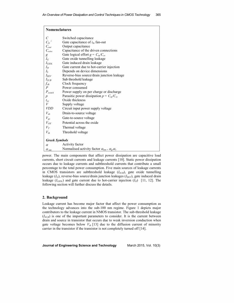
Nomenclatures
C Switched capacitance
CG i Gate capacitance of ith fan-out
Cout Output capacitance
Cwire Capacitance of the driven connections
g Gate logical effort g = Ctg/Csv
IG Gate oxide tunnelling leakage
IGIDL Gate induced drain leakage
IH Gate current due to hot-carrier injection
I0 Depends on device dimensions
IREV Reverse-bias source/drain junction leakage
ISUB Sub threshold leakage
fclk Clock frequency
P Power consumed
Pswitch Power supply on per charge or discharge
p Parasitic power dissipation p = Ctp/Csv
tox Oxide thickness
V Supply voltage
VDD Circuit input power supply voltage
Vds Drain-to-source voltage
Vgs Gate-to-source voltage
VOX Potential across the oxide
VT Thermal voltage
Vth Threshold voltage
Greek Symbols
α
α nm
Activity factor
Normalised activity factor αnm = αg/αv
power. The main components that affect power dissipation are capacitive load
currents, short circuit currents and leakage currents [10]. Static power dissipation
occurs due to leakage currents and subthreshold currents that contribute a small
percentage to the total power consumption. Five main sources of leakage currents
in CMOS transistors are subthreshold leakage (ISUB), gate oxide tunnelling
leakage (IG), reverse-bias source/drain junction leakages (IREV), gate induced drain
leakage (IGIDL) and gate current due to hot-carrier injection (IH) [11, 12]. The
following section will further discuss the details.
2. Background
Leakage current has become major factor that affect the power consumption as
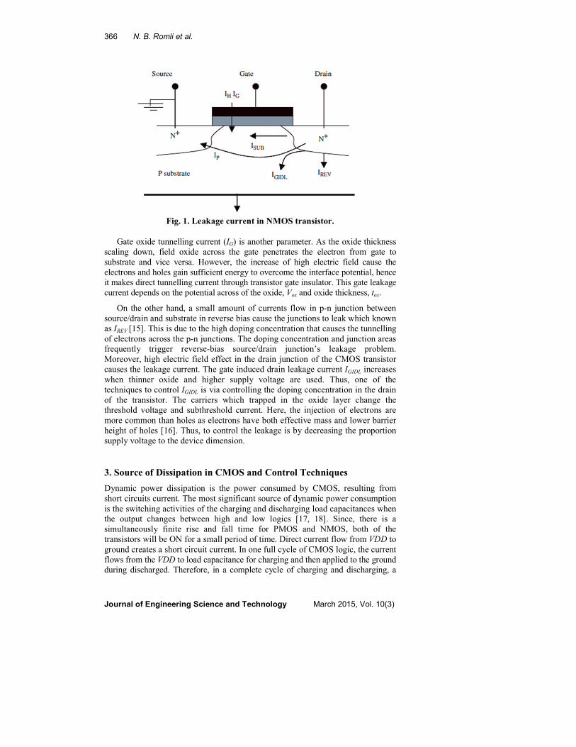
the technology advances into the sub-100 nm regime. Figure 1 depicts major
contributors to the leakage current in NMOS transistor. The sub-threshold leakage
(ISUB) is one of the important parameters to consider. It is the current between
drain and source in transistor that occurs due to weak inversion conduction when
gate voltage becomes below Vth [13] due to the diffusion current of minority
carrier in the transistor if the transistor is not completely turned off [14].
366 N. B. Romli et al.
Journal of Engineering Science and Technology March 2015, Vol. 10(3)
Fig. 1. Leakage current in NMOS transistor.
Gate oxide tunnelling current (IG) is another parameter. As the oxide thickness
scaling down, field oxide across the gate penetrates the electron from gate to
substrate and vice versa. However, the increase of high electric field cause the
electrons and holes gain sufficient energy to overcome the interface potential, hence
it makes direct tunnelling current through transistor gate insulator. This gate leakage
current depends on the potential across of the oxide, Vox and oxide thickness, tox.
On the other hand, a small amount of currents flow in p-n junction between
source/drain and substrate in reverse bias cause the junctions to leak which known
as IREV [15]. This is due to the high doping concentration that causes the tunnelling
of electrons across the p-n junctions. The doping concentration and junction areas
frequently trigger reverse-bias source/drain junction’s leakage problem.
Moreover, high electric field effect in the drain junction of the CMOS transistor
causes the leakage current. The gate induced drain leakage current IGIDL increases
when thinner oxide and higher supply voltage are used. Thus, one of the
techniques to control IGIDL is via controlling the doping concentration in the drain
of the transistor. The carriers which trapped in the oxide layer change the
threshold voltage and subthreshold current. Here, the injection of electrons are
more common than holes as electrons have both effective mass and lower barrier
height of holes [16]. Thus, to control the leakage is by decreasing the proportion
supply voltage to the device dimension.
3. Source of Dissipation in CMOS and Control Techniques
Dynamic power dissipation is the power consumed by CMOS, resulting from
short circuits current. The most significant source of dynamic power consumption
is the switching activities of the charging and discharging load capacitances when
the output changes between high and low logics [17, 18]. Since, there is a
simultaneously finite rise and fall time for PMOS and NMOS, both of the
transistors will be ON for a small period of time. Direct current flow from VDD to
ground creates a short circuit current. In one full cycle of CMOS logic, the current
flows from the VDD to load capacitance for charging and then applied to the ground
during discharged. Therefore, in a complete cycle of charging and discharging, a
An Overview of Power Dissipation and Control Techniques in CMOS Technology 367
Journal of Engineering Science and Technology March 2015, Vol. 10(3)
total of Q = CL. VDD is removed from the VDD to the ground. The performance of
dynamic power consumption can be improved by evaluating Eq. (1).
fCVP 2α= (1)
where, P is the power consumed, α the activity factor, C the switched
capacitance, V the supply voltage and f the clock frequency. A clock in a
system has activity factor of α = 1, since it rises and falls every cycle. Mostly
the activity factor of the data is 0.5. Dynamic power dissipation can be
computed effectively if the right load capacitance estimated at the nodes and
by factoring in the activity factors. It is crucial for designers and researchers
to take static and dynamic power dissipations into consideration in designing
low-power digital devices [19, 20]. Theoretically, dynamic logic has less
power dissipated compared to static logic due to the absence of output glitch
and capacitance reduction [21]. This can be deduced that dynamic CMOS
logics are more beneficial than static CMOS logic. Nevertheless, the pre-
charging operations that produce extra power dissipation do not influence the
static CMOS logic. However the rapid changes in process technology cause
the leakage power dissipation (static power) to increase much faster than
dynamic power and found dominant over the time. Power dissipation per
charge or discharge can be expressed by Eqs. (2) and (3).
2
2
1DDloadswitch
VCP = (2)
where, VDD is the power supply voltage and
wire
i
GloadCfanoutCiC +∑ ∈= (3)
given that iGC the gate capacitance of ith fan-out and Cwire the capacitance of the
driven connections [22]. Equations (2) and (3) show the relationship of total
capacitance and supply power effecting the power dissipation. At the
beginning, the power dissipation in CMOS devices is not a concern in chip
design. The focus is more on system speed and reliability. However, in deep
submicron technology, all consumed power commonly dissipated as heat and
the cost of providing power has caused great interest in power reduction [23].
VLSI designers must keep the balance in power dissipation and the
circuit’s performance with scaling of the devices. Scaling methods pay a
significant role in reducing the power dissipation from one technology node
to another node. There are various scaling methods used for VLSI circuits.
Traditionally, most common are voltage scaling, load scaling, technology
scaling and transistor sizing (width scaling). In voltage scaling for instance,
supply voltage plays a vital role for controlling the power consumption and
hence reducing the power dissipation. Moreover, threshold voltage of the
device must be reduced proportionally as supply voltage reduces to sustain
the transistor’s output performance. The reduction in threshold voltage
increases the leakage current drastically with each new technology generation.
The purpose of studying various scaling methods is to provide knowledge
for scaling while keeping power dissipation and propagation delay in mind.
There are techniques to minimise power dissipations and the possible control
technique in CMOS logic as discussed in the following section.
368 N. B. Romli et al.
Journal of Engineering Science and Technology March 2015, Vol. 10(3)
3.1. Dynamic and static power simultaneous reduction by using mapping technique
Scan-based test is one of the chosen techniques to solve power problem. This
method has become a popular design-for-test (DFT) procedure which gives
low impact on the area and at the same time maintaining the circuit
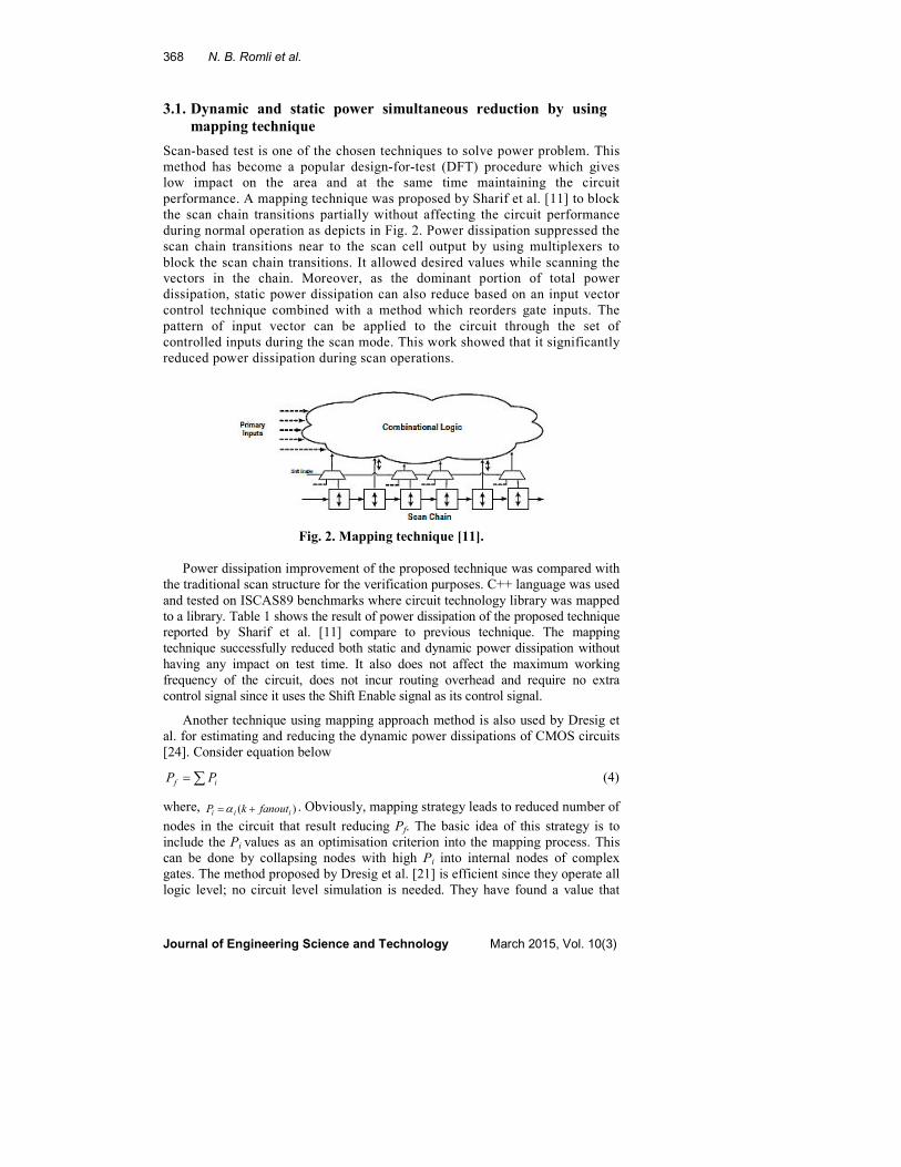
performance. A mapping technique was proposed by Sharif et al. [11] to block
the scan chain transitions partially without affecting the circuit performance
during normal operation as depicts in Fig. 2. Power dissipation suppressed the
scan chain transitions near to the scan cell output by using multiplexers to
block the scan chain transitions. It allowed desired values while scanning the
vectors in the chain. Moreover, as the dominant portion of total power
dissipation, static power dissipation can also reduce based on an input vector
control technique combined with a method which reorders gate inputs. The
pattern of input vector can be applied to the circuit through the set of
controlled inputs during the scan mode. This work showed that it significantly
reduced power dissipation during scan operations.
Fig. 2. Mapping technique [11].
Power dissipation improvement of the proposed technique was compared with
the traditional scan structure for the verification purposes. C++ language was used
and tested on ISCAS89 benchmarks where circuit technology library was mapped
to a library. Table 1 shows the result of power dissipation of the proposed technique
reported by Sharif et al. [11] compare to previous technique. The mapping
technique successfully reduced both static and dynamic power dissipation without
having any impact on test time. It also does not affect the maximum working
frequency of the circuit, does not incur routing overhead and require no extra
control signal since it uses the Shift Enable signal as its control signal.
Another technique using mapping approach method is also used by Dresig et
al. for estimating and reducing the dynamic power dissipations of CMOS circuits
[24]. Consider equation below
∑= if PP (4)
where, )( iii fanoutkP +=α . Obviously, mapping strategy leads to reduced number of
nodes in the circuit that result reducing Pf. The basic idea of this strategy is to
include the Pi values as an optimisation criterion into the mapping process. This
can be done by collapsing nodes with high Pi into internal nodes of complex
gates. The method proposed by Dresig et al. [21] is efficient since they operate all
logic level; no circuit level simulation is needed. They have found a value that
An Overview of Power Dissipation and Control Techniques in CMOS Technology 369
Journal of Engineering Science and Technology March 2015, Vol. 10(3)
they called power factor Pf which takes into account to technology parameter k
and suitable to compare different designs with regard to the average power
dissipation. They have introduced a new mapping strategy, taking into
consideration simulation results for minimising total power dissipation.
Table 1. Power dissipation of Sharif et al. and prior technique [11].
Traditional Scan
Structure Input Control
Proposed
Structure (µW)
Improvement
Compared with
Traditional Scan
(%)
Improvement
Compared with
Input Control
(%)
Dynamic
(/f)
(µW/Hz)
Static
(µW)
Dynamic
(/f)
(µW/Hz)
Static
(µW)
Dynamic
(/f)
(µW/Hz)
Static
(µW) Dynamic Static Dynamic Static
5.88E-8 27.99 5.72E-8 27.50 3.24E-8 23.89 44.82 14.65 43.23 13.12
6.43E-8 27.58 5.51E-8 26.69 2.38E-8 24.42 62.90 11.46 56.73 8.50
8.00E-8 33.72 6.92E-8 33.30 2.44E-8 27.99 69.44 17.00 64.67 15.95
8.46E-8 47.93 8.18E-8 47.50 8.22E-8 45.96 2.92 4.11 -0.41 3.24
5.69E-8 59.07 1.77E-8 56.97 1.78E-8 48.97 68.80 17.10 -0.50 14.05
6.30E-8 66.15 1.85E-8 64.90 1.82E-8 52.10 71.06 21.23 1.25 19.71
3.10E-8 115.54 3.06E-8 117.75 2.52E-8 95.78 18.61 17.09 17.50 18.65
3.19E-8 121.56 3.39E-8 124.75 2.59E-8 96.38 18.64 20.70 23.63 22.74
2.24E-7 128.22 1.93E-7 130.23 5.43E-8 117.00 75.77 9.02 71.83 10.43
3.56E-7 177.52 3.48E-7 179.86 3.52E-7 164.87 9.52 7.12 7.45 8.33
8.90E-7 327.52 1.29E-8 332.02 1.17E-8 315.00 98.68 3.82 9.50 5.12
1.50E-6 819.98 1.68E-8 854.52 1.57E-8 772.36 98.95 5.80 6.96 9.61
3.2. Optimisation technique
In 2008, Kabbani [18] developed a model and proposed an optimisation
technique to minimise the power consumption. The model developed by
normalising gate-switching power as a unit standard inverter and the effect of
internal node capacitances counted accordingly. In this normalised switching
power model, the first optimisation power technique was dealt with transistor
sizing and creates a scheme according to a specific design goal. The second
technique relies on the joint transistor sizing and supply voltage scaling for
reducing the switching power dissipation under specific delay requirements.
Concisely, power was widely known as
2
ddoutclkgVCfP α= (5)
where fclk is the clock frequency and Cout is the output capacitance. Kabbani
proposed expression is given by Eq. (6)
)pgh.(ZPnmnm
+=α (6)
where αnm is the normalised activity factor and is given as αnm = αg⁄αv, g is the gate
logical effort with given g= Ctg ⁄ Csv and p is the parasitic power dissipation where
p is given by p=Ctp ⁄ Csv. The performance of the developed model in [18] has been
tested in BSIM3v3 and UMC 0.13 µm technology by comparing modelling results
with the simulation result produced by Specters and shown in Figs. 3 and 4.
370 N. B. Romli et al.
Journal of Engineering Science and Technology March 2015, Vol. 10(3)
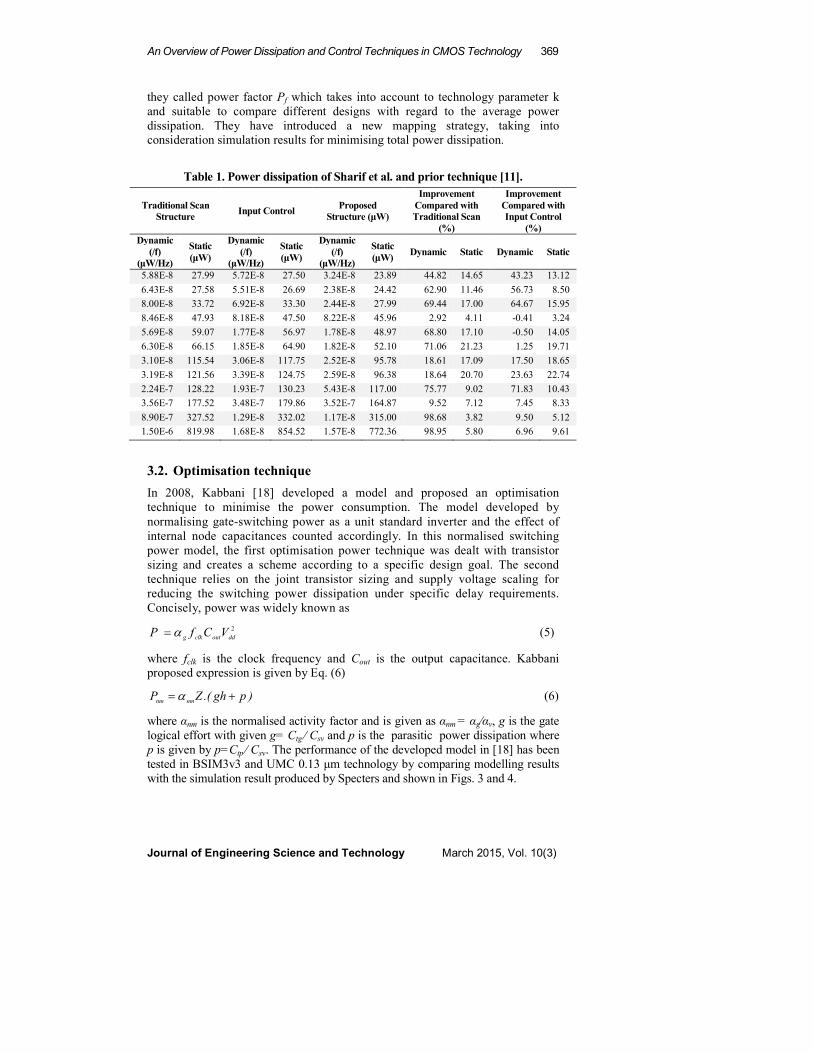
Figure 3 shows that the dissipated power of a design is proportional to the
total number of fanouts of the logic gates regardless the width of the buffer sizes.
Fanout simply refer to the total number of gate inputs can feed from the output
efficiently. In most designs, logic gates are connected to form more complex
circuits. Since it is common for one output to be connected to several inputs, it is
crucial for the logic gates to allow a certain number of gate inputs to be wired
directly together without additional interfacing circuitry.
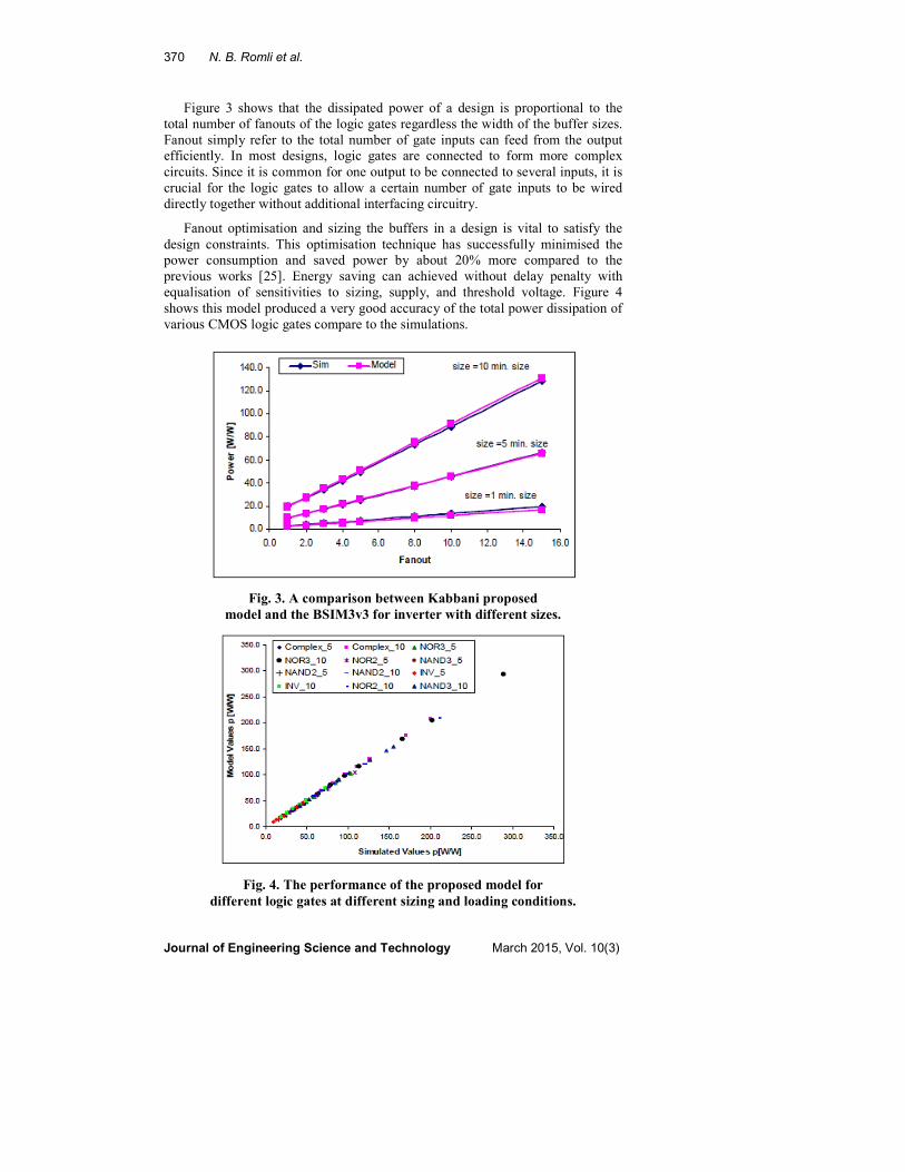
Fanout optimisation and sizing the buffers in a design is vital to satisfy the
design constraints. This optimisation technique has successfully minimised the
power consumption and saved power by about 20% more compared to the
previous works [25]. Energy saving can achieved without delay penalty with
equalisation of sensitivities to sizing, supply, and threshold voltage. Figure 4
shows this model produced a very good accuracy of the total power dissipation of
various CMOS logic gates compare to the simulations.
Fig. 3. A comparison between Kabbani proposed
model and the BSIM3v3 for inverter with different sizes.
Fig. 4. The performance of the proposed model for
different logic gates at different sizing and loading conditions.

An Overview of Power Dissipation and Control Techniques in CMOS Technology 371
Journal of Engineering Science and Technology March 2015, Vol. 10(3)
3.3. Multi-threshold CMOS (MTCMOS) technique
MTCMOS utilised transistors with multiple threshold voltages (Vt) to
optimise delay or power. Lower voltage devices were used on critical delay
paths to minimise clock periods. Higher voltage devices were used on non-critical
paths to reduce static leakage power without incurring a delay penalty. A common
MTCMOS approach to reduce power is the utilisation of sleep transistors.
MOS current mode logic has been implemented in MTCMOS technology
[26]. For decades, MTCMOS technology was used to reduce leakage in
standby mode and reached high speed in active mode as shown in Fig. 5. In
[26], the reduction of the operating supply voltage and level shifters
eliminations were used as shown in Fig. 6. A high-speed 1:8 2.5 GbiVs
demultiplexer was used as a test vehicle and 37% power saving was achieved.
Furthermore, the MTCMOS design showed no impact over circuit parameters such as
output impedance, gain, threshold voltage fluctuations and frequency response [26].
Fig. 5. MCML AND gate with level shifters (Conventional design).
Fig. 6. MTCMOS MCML AND gate [26].
372 N. B. Romli et al.
Journal of Engineering Science and Technology March 2015, Vol. 10(3)
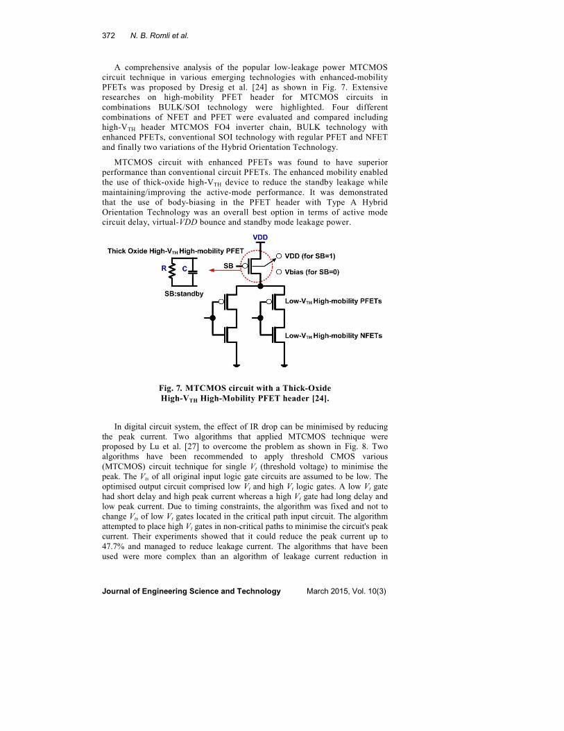
A comprehensive analysis of the popular low-leakage power MTCMOS
circuit technique in various emerging technologies with enhanced-mobility
PFETs was proposed by Dresig et al. [24] as shown in Fig. 7. Extensive
researches on high-mobility PFET header for MTCMOS circuits in
combinations BULK/SOI technology were highlighted. Four different
combinations of NFET and PFET were evaluated and compared including
high-VTH header MTCMOS FO4 inverter chain, BULK technology with
enhanced PFETs, conventional SOI technology with regular PFET and NFET
and finally two variations of the Hybrid Orientation Technology.
MTCMOS circuit with enhanced PFETs was found to have superior
performance than conventional circuit PFETs. The enhanced mobility enabled
the use of thick-oxide high-VTH device to reduce the standby leakage while
maintaining/improving the active-mode performance. It was demonstrated
that the use of body-biasing in the PFET header with Type A Hybrid
Orientation Technology was an overall best option in terms of active mode
circuit delay, virtual-VDD bounce and standby mode leakage power.
Fig. 7. MTCMOS circuit with a Thick-Oxide
High-VTH High-Mobility PFET header [24].
In digital circuit system, the effect of IR drop can be minimised by reducing
the peak current. Two algorithms that applied MTCMOS technique were
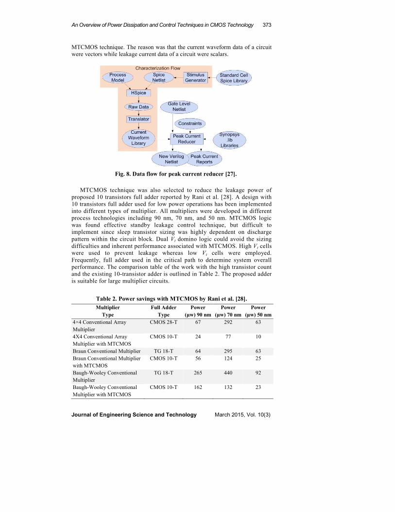
proposed by Lu et al. [27] to overcome the problem as shown in Fig. 8. Two
algorithms have been recommended to apply threshold CMOS various
(MTCMOS) circuit technique for single Vt (threshold voltage) to minimise the
peak. The Vts of all original input logic gate circuits are assumed to be low. The
optimised output circuit comprised low Vt and high Vt logic gates. A low Vt gate
had short delay and high peak current whereas a high Vt gate had long delay and
low peak current. Due to timing constraints, the algorithm was fixed and not to
change Vts of low Vt gates located in the critical path input circuit. The algorithm
attempted to place high Vt gates in non-critical paths to minimise the circuit's peak
current. Their experiments showed that it could reduce the peak current up to
47.7% and managed to reduce leakage current. The algorithms that have been
used were more complex than an algorithm of leakage current reduction in
An Overview of Power Dissipation and Control Techniques in CMOS Technology 373
Journal of Engineering Science and Technology March 2015, Vol. 10(3)
MTCMOS technique. The reason was that the current waveform data of a circuit
were vectors while leakage current data of a circuit were scalars.
Fig. 8. Data flow for peak current reducer [27].
MTCMOS technique was also selected to reduce the leakage power of
proposed 10 transistors full adder reported by Rani et al. [28]. A design with
10 transistors full adder used for low power operations has been implemented
into different types of multiplier. All multipliers were developed in different
process technologies including 90 nm, 70 nm, and 50 nm. MTCMOS logic
was found effective standby leakage control technique, but difficult to
implement since sleep transistor sizing was highly dependent on discharge
pattern within the circuit block. Dual Vt domino logic could avoid the sizing
difficulties and inherent performance associated with MTCMOS. High Vt cells
were used to prevent leakage whereas low Vt cells were employed.
Frequently, full adder used in the critical path to determine system overall
performance. The comparison table of the work with the high transistor count
and the existing 10-transistor adder is outlined in Table 2. The proposed adder
is suitable for large multiplier circuits.
Table 2. Power savings with MTCMOS by Rani et al. [28].
Multiplier
Type
Full Adder
Type
Power
(µw) 90 nm
Power
(µw) 70 nm
Power
(µw) 50 nm
4×4 Conventional Array
Multiplier
CMOS 28-T 67 292 63
4X4 Conventional Array
Multiplier with MTCMOS
CMOS 10-T 24 77 10
Braun Conventional Multiplier TG 18-T 64 295 63
Braun Conventional Multiplier
with MTCMOS
CMOS 10-T 56 124 25
Baugh-Wooley Conventional
Multiplier
TG 18-T 265 440 92
Baugh-Wooley Conventional
Multiplier with MTCMOS
CMOS 10-T 162 132 23

374 N. B. Romli et al.
Journal of Engineering Science and Technology March 2015, Vol. 10(3)
3.4. Forward body bias technique (FBB)
Current through NMOS upsizing transistors decreases significantly and degrade
the performance of circuits. On the other hands, more power is dissipated with the
NMOS upsizing. Circuit design techniques should not only be focused on
enhancing system speed but must also consider the power consumptions
concurrently. A forward body bias technique for 65 nm CMOS technology can
work under very low supply voltages (lower than VDD = 0.4 V) has been
proposed by Moradi et al. [29] as shown in Fig. 9. A domino logic circuit with
constant supply voltage was used.
Fig. 9. Domino logic circuit by Moradi et al. [29].
For a clearer picture, Fig. 10 illustrates the operation of adaptive supply
circuit. When “Clock” is low “0” whereby Clk_bar is in logic “1”, the supply
voltage node connects to the VDD. When “inputs” are all logic low (“0”), the
supply voltage decreases accordingly to reduce the power dissipation. Nevertheless,
when supply voltage is low, the reliability and the sensitivity of the circuit input
noise is deteriorates due to the reduction of on-current that passes through PMOS
keeper transistor in order to hold the dynamic node state. In this work, NMOS
device in the evaluation network are downsized to solve this noise issue.
A level shifter in TSMC 0.35µm process technology has been reported by [30]
for comparison purposes by using the similar input parameter. Table 3 shows the
proposed results of Moradi et al. with various bias voltages ranging from 0.1 V-
0.5 V of power consumption and delay for modified level shifter designs. The
proposed method reduced power consumptions significantly with a small delay
smaller than the previous reported circuits. Power consumptions reduced
significantly with the increase in reverse bias. Additionally, the slightly increase
in delay caused the increase in reverse bias voltage.

An Overview of Power Dissipation and Control Techniques in CMOS Technology 375
Journal of Engineering Science and Technology March 2015, Vol. 10(3)
Fig. 10. Waveforms of adaptive supply voltage by Moradi et al. [29].
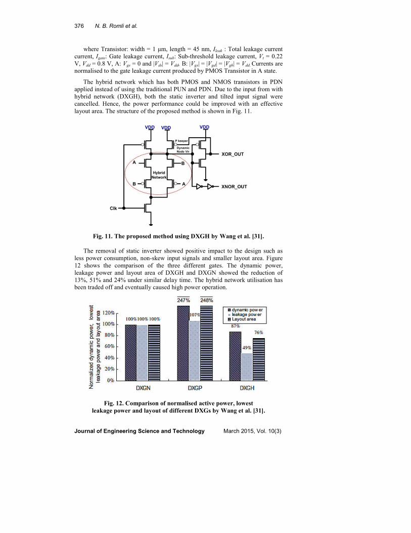
3.5. Hybrid network technique
A hybrid network technique in dynamic CMOS XOR / XNOR gate (DXG) based
on 45 nm Berkeley short-channel IGFET Model (BSIM4 model) has been
proposed by Wang et al. [31] to improve design signal skew. Moreover, it also
improved the power consumption and drawn in small layout. The main objective
was to investigate a better control of DXGP type which has greater leakage power
compared to DXGN due to greater barrier height in PMOS compared to NMOS.
On the other hands, DXGN has higher speed, thus the power consumption is high.
Table 4 shows the normalised leakage current of the devices at 25oC, where the
gate is static.
Table 3. Results of proposed level shifter circuit.
Bias
voltage
(V)
Level shifter configurations
Modified conventional
type-I level shifter
Modified conventional type-II
level shifter
Modified contention
level shifter
Power
Consumption
(pW)
Delay
(ns)
Power
Consumption
(pW)
Delay
(ns)
Power
Consumption
(pW)
Delay
(ns)
0.1 310.7590 2.7514 2209.7000 0.1120880 306.1605 0.3982240
0.2 205.6850 3.2149 1377.2000 0.1148531 201.0865 0.4048899
0.3 145.4804 3.6813 939.3620 0.1175174 140.8819 0.4117934
0.4 110.4990 4.4685 687.7304 0.1200811 105.9005 0.4198419
0.5 90.1250 5.3724 480.2857 0.1226488 85.5265 0.4275800
Table 4. Normalized leakage current of the devices at 25°C.
45 nm Technology NMOS PMOS
A: Ileak (Isub, Igate) 37.12 (19.59, 17.53) 16.56 (15.56, 1)
B: Igate 46.79 1.56
376 N. B. Romli et al.
Journal of Engineering Science and Technology March 2015, Vol. 10(3)
where Transistor: width = 1 µm, length = 45 nm, Ileak : Total leakage current
current, Igate: Gate leakage current, Isub: Sub-threshold leakage current, Vt = 0.22
V, Vdd = 0.8 V, A: Vgs = 0 and |Vds| = Vdd, B: |Vgs| = |Vgd| = |Vgb| = Vdd. Currents are
normalised to the gate leakage current produced by PMOS Transistor in A state.
The hybrid network which has both PMOS and NMOS transistors in PDN
applied instead of using the traditional PUN and PDN. Due to the input from with
hybrid network (DXGH), both the static inverter and tilted input signal were
cancelled. Hence, the power performance could be improved with an effective
layout area. The structure of the proposed method is shown in Fig. 11.
Fig. 11. The proposed method using DXGH by Wang et al. [31].
The removal of static inverter showed positive impact to the design such as
less power consumption, non-skew input signals and smaller layout area. Figure
12 shows the comparison of the three different gates. The dynamic power,
leakage power and layout area of DXGH and DXGN showed the reduction of
13%, 51% and 24% under similar delay time. The hybrid network utilisation has
been traded off and eventually caused high power operation.
Fig. 12. Comparison of normalised active power, lowest
leakage power and layout of different DXGs by Wang et al. [31].
An Overview of Power Dissipation and Control Techniques in CMOS Technology 377
Journal of Engineering Science and Technology March 2015, Vol. 10(3)
The dynamic CMOS XOR/XNOR gate also showed superior robustness under
process and temperature variation (PTV) which offered significant effect on leakage
current. In order to evaluate the impact of PTV on leakage current and dynamic power
characteristics of DXG, multiple–parameter Monte Carlo analysis is recommended.
3.6. Branch target buffer technique (BTB)
Three methods to reduce leakage power dissipated by using BTB is presented by
Khan et al. [32]. The methods used are window, awake line buffer (ALB) and 2-
level ALB (2L-ALB). The proposed methods are an important power components
in modern processor where leakage power dissipation is part of total power
dissipation. The findings showed that 2L-ALB reached additional reduction in
leakage power with no performance loss compared to ALB method [32]. The
extensive performance loss occured due to the increament of propagation delay as
VDD approaches 2VT. The problem could be resolved by reducing the threshold
voltage of the device. However, reducing the threshold voltage increases the
subthreshold current, which is limited by acceptable leakage of static power
dissipation [33]. 2L-ALB method can increase the power saving compared to
other methods with no power penalty. Concisely, the work showed that the power
dissipation in 2L-ALB reduced about 56% and the power dissipation of the entire
BTB reduced by 35%.
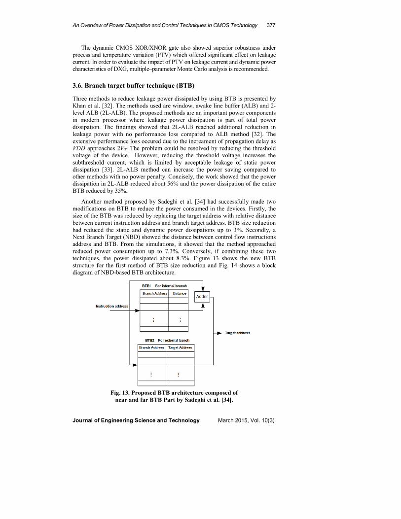
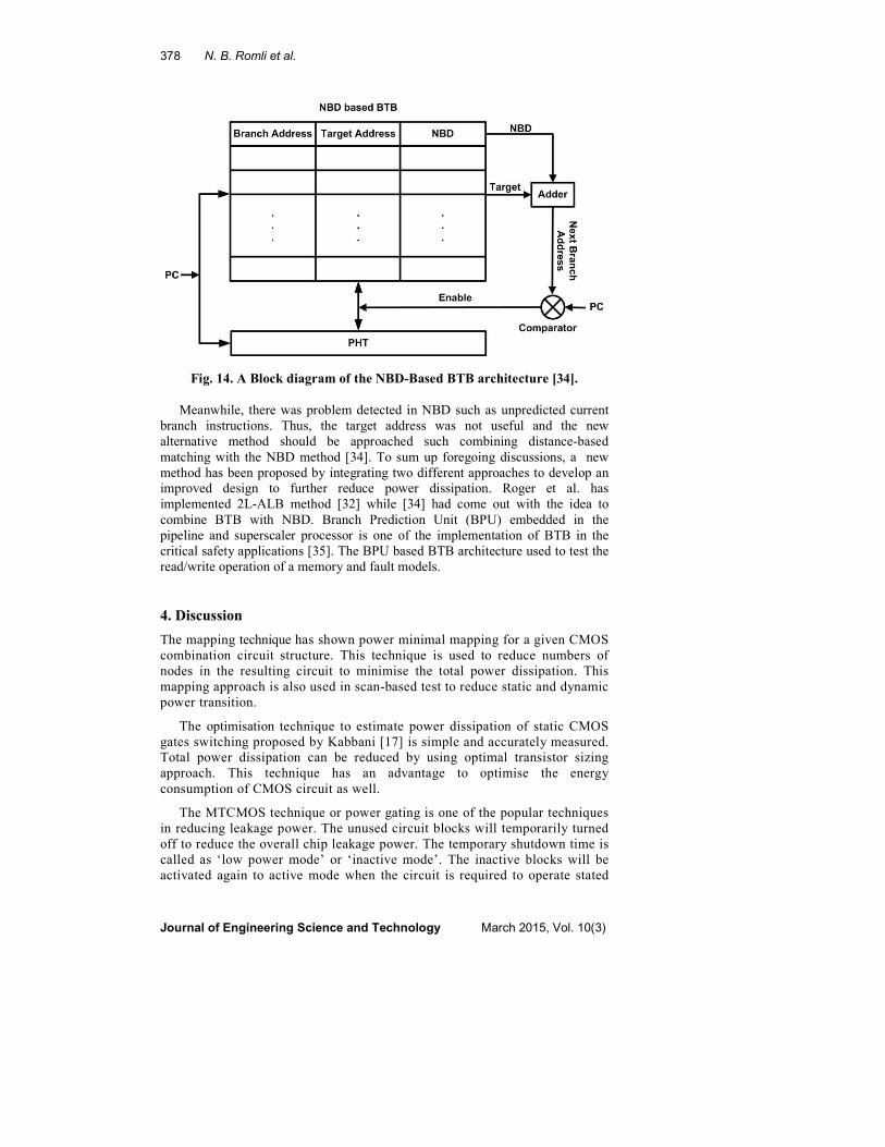
Another method proposed by Sadeghi et al. [34] had successfully made two
modifications on BTB to reduce the power consumed in the devices. Firstly, the
size of the BTB was reduced by replacing the target address with relative distance
between current instruction address and branch target address. BTB size reduction
had reduced the static and dynamic power dissipations up to 3%. Secondly, a
Next Branch Target (NBD) showed the distance between control flow instructions
address and BTB. From the simulations, it showed that the method approached
reduced power consumption up to 7.3%. Conversely, if combining these two
techniques, the power dissipated about 8.3%. Figure 13 shows the new BTB
structure for the first method of BTB size reduction and Fig. 14 shows a block
diagram of NBD-based BTB architecture.
Fig. 13. Proposed BTB architecture composed of
near and far BTB Part by Sadeghi et al. [34].
378 N. B. Romli et al.
Journal of Engineering Science and Technology March 2015, Vol. 10(3)
Fig. 14. A Block diagram of the NBD-Based BTB architecture [34].
Meanwhile, there was problem detected in NBD such as unpredicted current
branch instructions. Thus, the target address was not useful and the new
alternative method should be approached such combining distance-based
matching with the NBD method [34]. To sum up foregoing discussions, a new
method has been proposed by integrating two different approaches to develop an
improved design to further reduce power dissipation. Roger et al. has
implemented 2L-ALB method [32] while [34] had come out with the idea to
combine BTB with NBD. Branch Prediction Unit (BPU) embedded in the
pipeline and superscaler processor is one of the implementation of BTB in the
critical safety applications [35]. The BPU based BTB architecture used to test the
read/write operation of a memory and fault models.
4. Discussion
The mapping technique has shown power minimal mapping for a given CMOS
combination circuit structure. This technique is used to reduce numbers of
nodes in the resulting circuit to minimise the total power dissipation. This
mapping approach is also used in scan-based test to reduce static and dynamic
power transition.
The optimisation technique to estimate power dissipation of static CMOS
gates switching proposed by Kabbani [17] is simple and accurately measured.
Total power dissipation can be reduced by using optimal transistor sizing
approach. This technique has an advantage to optimise the energy
consumption of CMOS circuit as well.
The MTCMOS technique or power gating is one of the popular techniques
in reducing leakage power. The unused circuit blocks will temporarily turned
off to reduce the overall chip leakage power. The temporary shutdown time is
called as ‘low power mode’ or ‘inactive mode’. The inactive blocks will be
activated again to active mode when the circuit is required to operate stated

An Overview of Power Dissipation and Control Techniques in CMOS Technology 379
Journal of Engineering Science and Technology March 2015, Vol. 10(3)
by Das et al. [36]. The proposed technique has successfully reduced the
standby leakage and maintained the active-mode performance. MTCMOS
technique has been used by Lu et al. reported in [27] where algorithms
proposed to reduce the peak current. Their proposed technique with
MTCMOS approach has successfully reduced the peak current up to 47% and
also the leakage current. MTCMOS approach was also used Rani et al. [28] to
reduce the leakage power by placing MTCMOS cell as a header and footer for
the proposed 10 transistors full adder. The proposed technique has
successfully improved the leakage power. However, Anis and Elmasry in [26]
have a different approach from the reviewed works in implementing MTCMOS
technique. MTCMOS was not used to reduce leakage power in the standby mode.
Instead, it used to reduce the power supply and to ensure the correct function in
active mode. The proposed work shown that 37% reduction in power saving and
have no impact over circuit parameters.
FBB technique implementation in ultra-low supply voltages suitable for
high speed circuits like domino logic circuit. The technique used to increase
the speed while lower power dissipation is maintained by introducing lower
supply voltages. The optimised bulk voltages discovered can boost the circuit to the
maximum speed. The method proposed was found efficient as the little concession
in delay has reduced the power significantly with the increment in reverse bias.
Thus, NMOS upsized is not a mandatory to have successful evaluation.
In hybrid network technique, DXGH was used extensively especially in
modern high performance microprocessor to decrease both leakage power and
dynamic power about 51% and 13% respectively as compared to the DXGN.
Thus, this approached success in achieving high power and speed operations
without input signal skew.
The BTB technique reported that the leakage power dissipated in BTB
reduced to 56% and BTB overall power reduction was recorded about 35%.
The NBD-based BTB however consumed almost 7.3% of the processor power
and the total energy gain has increased almost 8.3% in the microprocessor.
5. Conclusions
Various techniques used by researchers in order to get low power dissipations in
CMOS technology. By reducing power dissipation, power consumptions can be
optimised, thus make the electronic circuits more reliable. In this review, we
presented a few techniques proposed by previous study such as mapping technique,
optimisation technique, MTCMOS technique, forward body bias (FBB) technique,
hybrid network technique and branch target buffer (BTB) technique and
successfully reduced the power dissipation. This review serves its purpose to
provide initial guideline for the researches.
References
1. Jalil, J.; Bin Ibni Reaz, M.; and Ali, M.A.M. (2013). CMOS differential ring
oscillators: review of the performance of CMOS ROs in communication
systems. IEEE Microwave Magazine, 14(5), 97-109.
380 N. B. Romli et al.
Journal of Engineering Science and Technology March 2015, Vol. 10(3)
2. Mohd-Yasin, F.; Khaw, M.K.; and Reaz, M.B.I. (2006). Radio frequency
identification: Evolution of transponder circuit design. Microwave Journal,
49(6), 56-70.
3. Uddin, J.; Reaz, M.B.I.; Hasan, M.A.; Nordin, N.I.; Ibrahimy, M.I.; and Ali,
M.A.M. (2010). UHF RFID antenna architectures and applications. Scientific
Research and Essays, 5(10), 1033-1051.
4. Uddin, M.J.; Ibrahimy, M.I.; Reaz, M.B.I.; and Nordin, A.N. (2009). Design
and application of radio frequency identification systems. Journal of
European Science Research, 33(3), 438-453.
5. Teh, Y.K.; Mohd-Yasin, F.; Choong, F.; Reaz, M.I.; and Kordesch, A.V.
(2009). Design and analysis of UHF micropower CMOS DTMOST rectifiers.
IEEE Transactions Circuits and Systems II: Express Briefs, 56(2), 122-126.
6. Mohd-Yasin, F.; Yap, M.T.; and Reaz, M.B.I. (2007). CMOS
instrumentation amplifier with offset cancellation circuitry for biomedical
application. WSEAS Transactions Circuits and Systems, 6(1), 171-174.
7. Mohd-Yasin, F.; Khaw, M.K.; and Bin Ibne Reaz, M. (2006). Techniques of
RFID systems: Architectures and applications. Microwave Journal, 49(7),
62-74.
8. Yasin, F.M.; Tye, K.F.; and Reaz, M.B.I. (2005). Design and implementation
of interface circuitry for CMOS-based SAW gas sensors. Proceedings of
IEEE SOC Conference, 161-164.
9. Khaw, M.K.; Mohd-Yasin, F.; and Reaz, M.B.I. (2004). Recent advances in
the integrated circuit design of RFID transponder. Proceedings of IEEE
Semiconductor Electronics Conference, 326-330.
10. Hanchate, N.; and Ranganathan, N. (2004). A new technique for leakage
reduction in CMOS circuits using self-controlled stacked transistors.
Proceedings of VLSI Design Conference, 228-233.
11. Sharifi, S.; Jaffari, J.; Hosseinabady, M.; Afzali-Kusha, A.; and Navabi, Z.
(2005). Simultaneous reduction of dynamic and static power in scan
structures. Proceedings of Design, Automation and Test Conference, Munich,
2, 846-851.
12. Ndubuisi, E.; and Etienne-Cummings, R. (2006). Power dissipation sources
and possible control techniques in ultra-deep submicron CMOS technologies.
Microelectronics Journal, 37(9), 851-860.
13. Elgharbawy, W.M.; and Bayoumi, M.A. (2005). Leakage sources and
possible solutions in nanometer CMOS technologies. IEEE Circuits Systems
Magazine, 5(4), 6-17.
14. Butzen, P.F.; Rosa Jr, L.S.; Chiappetta Filho, E.J.D.; Reis, A.I.; and Ribas,
R.P. (2010). Standby power consumption estimation by interacting leakage
current mechanisms in nanoscaled CMOS digital circuits. Microelectronics
Journal, 41(4), 247-255.
15. Rabaey, M.; Chandrakasan, A.; and Nikolic, B. (2003). Digital Integrated
Circuits. 2nd
Edition, Pearson, New Delhi, India.
16. Roy, K.; Mukhopadhyay, S.; and Mahmoodi-Meimand, H. (2003). Leakage
current mechanisms and leakage reduction techniques in deep-submicrometer
CMOS circuits. Proceedings of IEEE 91, 2(2), 305–327.
An Overview of Power Dissipation and Control Techniques in CMOS Technology 381
Journal of Engineering Science and Technology March 2015, Vol. 10(3)
17. Kabbani, A. (2008). Modelling and optimisation of switching power
dissipation in static CMOS circuits. IEEE Computer Society Annual
Symposium, 281-285.
18. Kabbani, A. (2010). Logical effort based dynamic power estimation and
optimisation of static CMOS circuits. Journal of VLSI, 43(3), 279-288.
19. Chandrakasan, A.P.; Sheng, S.; and Brodersen, R.W. (1992). Low-power
CMOS digital design. IEEE Journal of Solid-State Circuits, 27(4), 473-484.
20. Chandrakasan, A.P.; and Brodersen, R.W. (1995). Minimising power
consumption in digital CMOS circuits. Proceedings of IEEE, 83(4), 498-523.
21. Macii, E.; and Poncino, M. (1996). Power consumption of static and dynamic
CMOS circuits: a comparative study. Proceedings in ASIC Conference,
425-427.
22. Klab, S.; Napieralski, A.; and De Mey, G. (2009). Logi-thermal simulation of
digital CMOS ICs with emphasis on dynamic power dissipation. Proceedings
of Mixed Design Integrated Circuits Systems, 361- 365.
23. Romli, N.B.; Mamun, M.; Bhuiyan, M.A.S.; and Husain, H. (2012). Design
of a low power dissipation and low input voltage range level shifter in
Cedec 0.18-µm CMOS process. Journal of World Applied Science, 19(8),
1140-1148.
24. Dresig, F.; Lanches, P.; Rettig, O.; and Baitinger, U.G. (1993). Simulation
and reduction of CMOS power dissipation at logic level. Proceedings of
Design Automation Conference, 341-346.
25. Rezvani, P.; Ajami, A.H.; Pedram, M.; and Savoj, H. (1999). Leopard: a
logical effort-based fanout optimiser for area and delay. Proceedings of IEEE
ICCAD Conference, 516-519.
26. Anis, M.H.; and Elmasry, M.I. (2002). Power reduction via an MTCMOS
implementation of MOS current mode logic. Proceedings of IEEE ASIC/SOC
Conference, 193-197.
27. Lu, L.Y.; Wu, T.Y.; Chiou, L.Y.; and Shi, J.W. (2010). Peak current
reduction using an MTCMOS technique. Proceedings of Quality Electronic
Design Symposium, 255-259.
28. Rani, T.E.; and Rao, R. (2011). Area and power optimised multipliers with
minimum leakage. Proceeding of Electronics Computer and Technology
Conference, 3, 284-287.
29. Moradi, F.; Wisland, D.T.; Mahmoodi, H.; Cao, T.V.; and Dooghabadi, M.Z.
(2009). Adaptive supply voltage circuit using body bias technique.
Proceedings of Mixed Design Integrated Circuits and Systems Conference,
215-219.
30. Kumar, M.; Arya, S.K.; and Pandey, S. (2010). Level shifter for low power
applications with body bias technique. Journal of Engineering Science and
Technology, 2(6), 297-305.
31. Wang, J.; Gong, N.; Hou, L.; Peng, X.; Geng, S.; and Wu, W. (2011). Low
power and high performance dynamic CMOS XOR/XNOR gate design.
Microelectronic Engineering, 88(8), 2781-2784.
32. Kahn, R.; and Weiss, S. (2010). Reducing leakage power with BTB access
prediction. Journal of Integrated VLSI, 43(1), 49-57.
382 N. B. Romli et al.
Journal of Engineering Science and Technology March 2015, Vol. 10(3)
33. Rabaey, J.M.; Chandrakasan, A.; and Nikolic, B. (2003). Digital integrated
circuits: A design perspective. 2nd
Edition, Prentice-Hall, Englewood Cliffs, NJ.
34. Sadeghi, H.; Sarbazi-Azad, H.; and Zarandi, H.R. (2009). Power-aware
branch target prediction using a new BTB architecture. Proceedings of VLSI-
SoC Conference, 53-58.
35. Changdao, D.; Graziano, M.; Sanchez, E.; Sonanza, R.M.; Zamboni, M.; and
Zhifan, N. (2013). On the functional test of the BTB logic in pipelined and
superscalar processors. IEEE Test Workshop, 1-6.
36. Das, K.K.; Lo, S.-H.; and Chuang, C.-T. (2006). High performance
MTCMOS technique for leakage reduction in hybrid SOI-Epitaxial
technology with enhanced-mobility PFET header. Proceedings of IEEE 5th
International on Embedded Systems and Design and 19th
International
Conference on VLSI Design.