an algorithm for synthesis of asychronous … algorithm for synthesis of ... sequential circuit...
TRANSCRIPT

I. 1 * . - 1
AN ALGORITHM FOR SYNTHESIS OF ASYNCHRONOUS SEQUENTIAL CIRCUITS
by John SI Tr@p Langley Research Center Langley Station, Hampton, Va.
N A T I O N A L AERONAUTICS A N D SPACE A D M I N I S T R A T I O N W A S H I N G T O N
I
i
il
https://ntrs.nasa.gov/search.jsp?R=19660030607 2018-07-17T16:32:15+00:00Z

TECH LIBRARY KAFB, NM
I 111111 lllll lllllll1ll1ll1 Illl It Ill 1111 1111 0079797
NASA '1" U - Y Z ' l Y
AN ALGORITHM FOR SYNTHESIS
OF ASYNCHRONOUS SEQUENTIAL CIRCUITS
By John S. Tripp
Langley Research Center Langley Station, Hampton, Va.
NATIONAL AERONAUTICS AND SPACE ADMlN ISTRATION ~.
For sale by the Clearinghouse for Federal Scientific and Technical Information Springfield, Virginia 22151 - Price $1.00

AN ALGORITHM FOR SYNTHESIS
OF ASYNCHRONOUS SEQUENTIAL CIRCUITS*
By John S. Tripp Langley Research Center
SUMMARY
An algorithm for synthesis of asynchronous sequential circuits is devel- oped; this development is an extension of the well-known Boolean methods for synthesis of synchronous circuits. A matrix system of f'unction representation is introduced and utilized in the execution of the algorithm. As an example, a six-count counter is synthesized with synchronous and asynchronous designs. Both designs are presented for comparison.
INTRODUCTION
A sequential switching circuit is a black box having inputs, outputs, and a number of possible internal states. The values of the inputs, outputs, and the internal state are considered at periodic intervals of time, known as bit times. At a given bit time, the internal state is determined by the inputs and internal state at the previous bit time; the outputs are determined by the inputs and internal state at the present bit time (ref. 1, p. 144). poses of the present paper, a sequential switching circuit is defined as an interconnection of logical and memory elements, where the internal state is the set-reset pattern of the memory elements.
For pur-
Sequential circuit designs may be classed as being either synchronous or asynchronous. The class to which a circuit belongs is determined by the source of the switching commands to the memory elements. In a synchronous sequential circuit, those memory elements which are to be switched during each internal- state change do so simultaneously under command of a central pulse source or clock. In the asynchronous sequential circuit, however, the switching pulse is derived from the switching action or transition of another memory element. During each internal-state change the memory elements are switched in a chain reaction, which can result in significant delays and may lead to timing
The information presented herein is largely based on a paper entitled * "Design of Asynchronous Sequential Circuits Using Boolean Algebra" by John S. Tripp published in Proceedings of the Central States Simulation Council Meeting on Analog Computation and Allied Digital Problems, Special Rept. No. 37, Kansas State Univ. Bull., vol. 47, no. 9, Sept. 1963.

di f f icu l t ies . ber of logic elements required i s usually less , sometimes considerably less , than tha t f o r an equivalent synchronous design.
However, an asynchronous design has the advantage that the num-
Formal procedures f o r the synthesis of synchronous sequential c i r cu i t s using Boolean algebra a re presented i n d e t a i l i n the l i t e r a tu re . asynchronous c i r cu i t s has been l imited t o nonanalytic procedures and the designer's ingenuity. include asynchronous c i r cu i t s and develops a matrix system of function repre- sentation which a ids i n the performance of the synthesis procedure.
Synthesis of
This paper extends the synchronous synthesis methods t o
General :
A, B, c
D
E
H
IP
mk
P
f l ip - f lop stages
a rb i t ra ry Boolean function
f l ip - f lop enable input
general Boolean functions
kth function value of f
Boolean constraining function
general input of memory element
cardinali ty of the se t
kth minterm
A' Ip) (
QP
f l ip- f lop pulse input
internal s t a t e of kth memory element a t time n
reset input of f l ip-f lop Ap
se t input of f l ip-f lop Ap
reset enable input f o r f l ip - f lop
se t enable input for f l ip-f lop
"don't care" condition
Ap
Ap
2
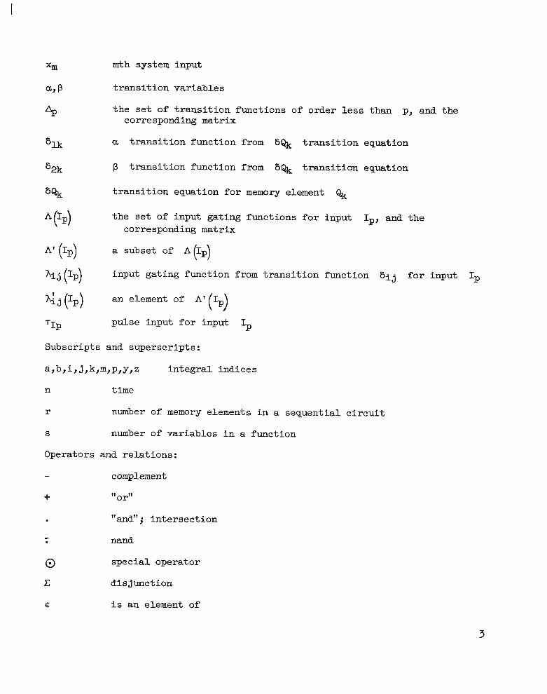
I
mth system input
transition variables
the set of transition functions of order less than p, and the corresponding matrix
a transition function from 8% transition equation
p transition function from 8% transition equation
transition equation for memory element
the set of input gating functions for input
C& Ip, and the
corresponding matrix
a subset of A I
input gating function from transition function 6ij for input Ip
an element of A' I
pulse input for input Ip
( p)
( 4 Subscripts and superscripts:
a,b,i,J,k,m,p,y,z integral indices
n time
r number of memory elements in a sequential circuit
S number of variables in a function
Operators and relations:
- complement
+ '' or"
'' and" ; inters e c t ion
nand
0 special operator
c disjunction
E is an element of
-
3
s e t inclusion
i s l e s s than
i s l e s s than o r equal t o
TYPICAL LOGIC CIRCUITS
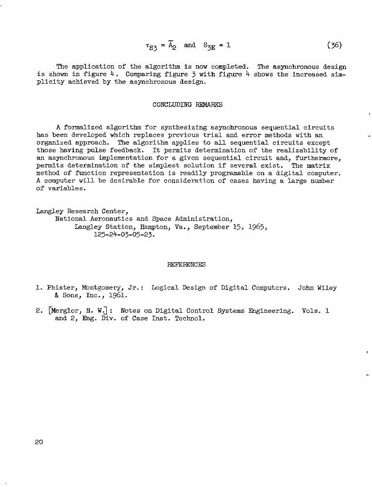
Logic c i r cu i t s suitable f o r use with asynchronous Lzsigns a re i l l u s t r a t ed i n figures 1 and 2. Figure 1 shows a typ ica l resistor-coupled t rans is tor inverting gate. A typical ac coupled set-reset f l ip-f lop c i r cu i t which i s well suited f o r both synchronous and asynchronous designs i s shown i n figure 2. The f l ip - f lop is switched only by satisfying cer ta in conditions on a pulse-enable (P-E) input pair . The pulse (P) input receives a switching pulse, which may e i the r be enabled o r blocked by the condition existing on the enable (E) input of the pair . To provide "or" gating, several pa i r s of pulse and enable inputs may be provided on both the set and reset sides of each f l ip-f lop. f l ip - f lop i s available commercially from a large number of manufacturers. For the par t icular c i rcu i t i n figure 2, i f the enable (E) input i s held a t ground, then a voltage t rans i t ion from the posit ive leve l t o ground on the pulse input w i l l r esu l t i n a switching command. A posit ive voltage on the enable input w i l l block the effect of t ransi t ions on the pulse input. A voltage t rans i t ion from ground t o the posit ive leve l w i l l be ignored regardless of the condition a t the l eve l input.
This type of
REVIEW OF SYNCHRONOUS SYNTHESIS METHODS
Details of synchronous synthesis procedures a re well presented i n refer- ence 1. Any logical memory element may have i t s operation represented by a Boolean equation i n which i t s in te rna l s ta te , a f t e r being subject t o a switching command, i s expressed as a function of the inputs and the previous in te rna l s t a t e . This equation i s known as the character is t ic equation of the element. Let the internal s t a t e at time n be represented by Qn, and the s t a t e a t time n + 1 a f t e r receiving a clock pulse be Qn+'. For an R-S f l ip-f lop the character is t ic equation i s
with the constraint that RS = 0. The following general character is t ic equa- t ion i s a Boolean difference equation:
Qn+' = f(Qn, XI, =, XIU)
4
with the constraint tha t H xl, . ., = 0, where xl, . . ., Xm a re
inputs . Operation of any sequential switching c i r cu i t consisting of k memory ele-
ments may be represented by k Boolean difference equations. These expressions a re known as application equations and each expresses the s t a t e corresponding memory device a t time
Q~+' of i t s n. A general application equation i s
where Ql, . . ., Qr a re the r memory-element stages, and xl, . . ., % are the m system inputs.
By solving the application equation (eq. ( 3 ) ) of f l ip-f lop Q simultane- ously with the character is t ic equation (eq. (l)), a s e t of input equations i s obtained; each equation represents a required gating function t o be provided t o a memory element input. For ac coupled f l ip-f lops the gating function deter- mines the required gating structures into each enable input. A clock feeds a l l pulse inputs.
ASYNCRRONOUS SYNTHESIS - BASIC CONSIDERATIONS
The asynchronous synthesis technique presented herein i s useful only f o r implementation of sequential c i r cu i t s whose switching sequences have been spec- i f i e d and f o r which input equations have been determined a s f o r a synchronous design. Circuits having pulse feedback are not eas i ly considered.
Let f l ip-f lop c i r cu i t s having pulse and enable inputs, as i n figure 2, be used. An association of voltage levels and logic values w i l l be made by l e t t i n g the enabling voltage l eve l be associated with log ica l "1."
Logical t rans i t ion variables similar t o those i n reference 2 a re now defined. Consider a Boolean variable Qk. If it i s t rue that, during the t i m e t rans i t ion from n t o n + 1, Qk goes from "0" t o "l", then an a t rans i t ion has occurred, and the a t rans i t ion function 6~ equals 1j otherwise 6- equals 0. Correspondingly, i f Qk goes from "1" t o "0" , a p t rans i t ion has occurred and the p t rans i t ion function 62k equals 1j otherwise 62k eqU.alS 0. It i s seen tha t 6- and 62k are mutually exclusive.
A s shown i n reference 1, the general application equation i s
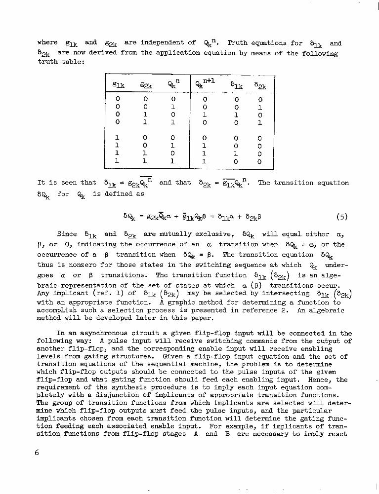
where glk and g2k are independent of &n. Truth equations for 61k and
62k truth table:
are now derived from the application equation by means of the following
0 0 0 0
1 1 1 1
0 0 1 1
0 0 1 1
0 1 0 1
0 1 0 1 1
. ~~ _- _ _ _ _ ~
0 0 0 0 0 1 1 1 0 0 0 1
0 0 0 1 0 0 1 1 0 1 0 0
- - It is seen that 61k = g2kQkn and that 62k = glkQkn. The transition equation 6Qk for Qk is defined as
Since 6lk and 62k are mutually exclusive, 6Qk will equal either a, p, or 0, indicating the occurrence of an a transition when 6% = a, or the occurrence of a p transition when 6% = p. The transition equation 6% thus is nonzero for those states in the switching sequence at which goes a or p transitions. The transition function 6Lk (62k) is an alge- braic representation of the set of states at which a ( p ) transitions occur. b y implicant (ref. 1) of 6 a (82k) may be selected by intersecting (62k) with an appropriate function. A graphic method for determining a function to accomplish such a selection process is presented in reference 2. An algebraic method will be developed later in this paper.
% under-
In an asynchronous circuit a given flip-flop input will be connected in the A pulse input will receive switching commands from the output of following way:
another flip-flop, and the corresponding enable input will receive enabling levels from gating structures. Given a flip-flop input equation and the set of transition equations of the sequential machine, the problem is to determine which flip-flop outputs should be connected to the pulse inputs of the given flip-flop and what gating function should feed each enabling input. requirement of the synthesis procedure is to imply each input equation com- pletely with a disjunction of implicants of appropriate transition functions. "he group of transition functions from which implicants are selected will deter- mine which flip-flop outputs must feed the pulse inputs, and the particular implicants chosen from each transition function w i l l determine the gating func- tion feeding each associated enable input. For example, if implicants of tran- sition functions from flip-flop stages A and B are necessary to imply reset
Hence, the
6
input function Rk, A and B will each feed a pulse input on Rk, and gating levels selecting the desired implicants from the transition functions of A and B w i l l feed the associated enable inputs on Rk.
The flip-flops of the sequential circuit must be ordered to determine the propagation sequence of switching commands. may be difficult and is affected by the following considerations: Generally the flip-flops undergoing transitions most frequently in the switching sequence should precede those undergoing transitions less frequently. One or more of the flip-flops undergoing transitions most frequently will be chosen to receive clock pulses, so that the totality of their transition functions contain com- plete implication f o r input functions of following flip-flops. For circuits with several flip-flops, propagation delays in switching transitions may result in an enabling level changing before the arrival of its associated switching transition. Hence, the ordering must be such that all enabling functions which change with their associated switching transitions have propagation delays at least as great as those of the transition delay. A method for determining an ordering will be presented later.
Determination of the best ordering
Assume that flip-flop pulse inputs respond to 0 to 1, or a, transitions. Then if an implicant of the a transition function, 61k, of flip-flop & is an implicant for the input function will be connected to the pulse input of Ip. If an implicant of the j3 tran- sition function, 62k, of Qk is a desired implicant for Ip, the negated or "false" output of & will feed the pulse input of Ip.
Ip, the asserted or "true" output of &
When several transition sources are required to imply input Ip, redundant implication of some minterms (ref. 1) of Ip may result. If the delay between redundant input transitions is greater than the recovery time of the flip-flop and if multiple activation of that input cannot be allowed, as with "T" inputs, the selection of implicants must be nonredundant to avoid unwanted switching. If no implicants for certain minterms of exist in the set of appropriate transition equations, clock pulses may be used.
Ip
FORMAL SYNTHESIS DEVELOPMENT
The basis for the formal synthesis procedure is now developed. Assume that all design steps of the synchronous procedure have been carried out through the determination of input equations and that a transition equation has been obtained from each application equation. Let a general input equation be
7
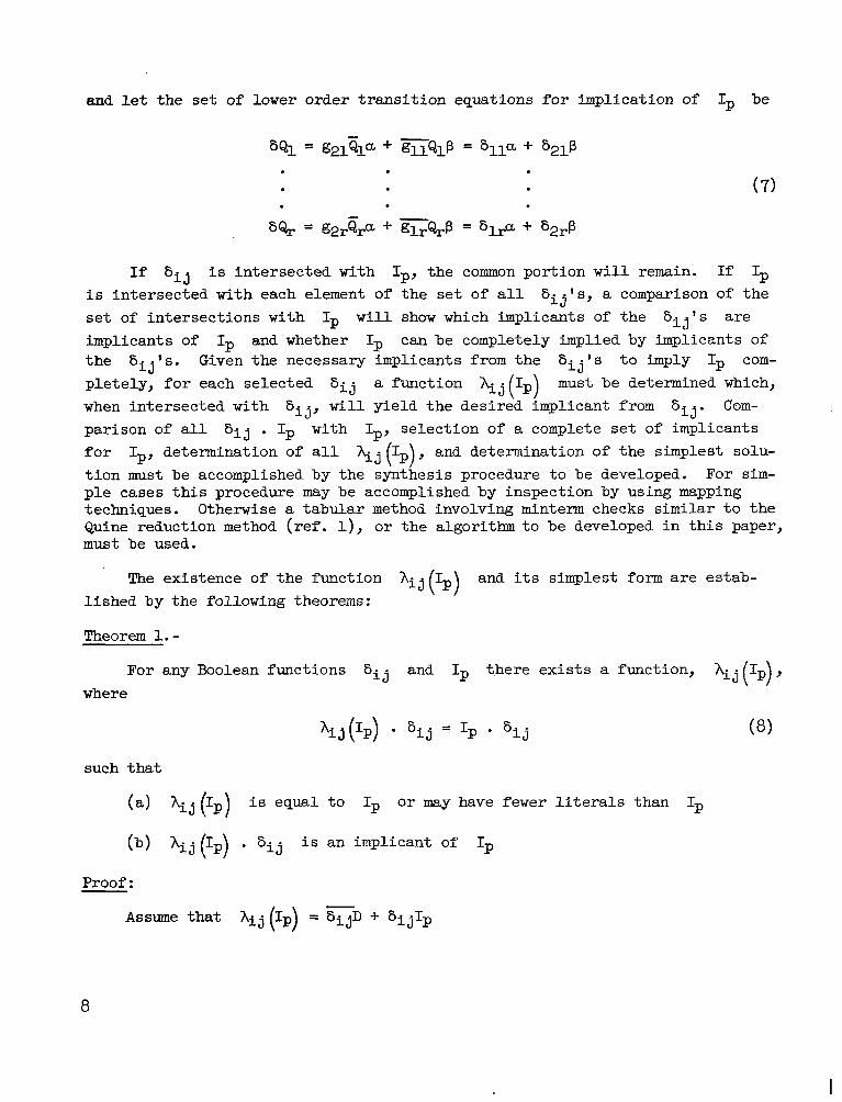
and let the set of lower order transition equations for implication of Ip be
If 813 is intersected with Ip, the common portion will remain. If Ip is intersected with each element of the set of all Gijls, a comparison of the set of intersections with Ip will show which implicants of the Gij's are implicants of Ip and whether Ip can be completely implied by Fmplicants of the G i j ' s . Given the necessary implicants from the Gijls to imply Ip cam- pletely, for each selected 6ij must be determined which, when intersected with 6ij, w i l l yield the desired implicant from Gij. Com- parison of all 6ij . Ip with Ip, selection of a complete set of implicants for Ip, determination of all hij (Ip), and determination of the simplest solu- tion must be accomplished by the synthesis procedure to be developed. For sim- ple cases this procedure may be accomplished by inspection by using mapping techniques. Otherwise a tabular method involving minterm checks similar to the Quine reduction method (ref. l), or the algorithm to be developed in this paper, must be used.
a function % (Ip)
The existence of the function hij and its simplest form are estab- lished by the following theorems:
Theorem 1. -
where For any Boolean functions 6ij and Ip t,here exists a function, hj (Ip),
such that
Proof:
Assume that
5 P (I ) . Gij = Ip . 'ij
is equal to Ip o r may have fewer literals than Ip
. zij is an implicant of Ip
8
I
- and 6ijD + 6 i j Ip i s such a function; hence, the existence of A i j (Ip)
- (a ) Choose D = Ip+ Then hij(1p) = 6ijI-p + 6 i j I p = Ip-
Thus h i j (Ip) may always be made equal t o Ip.
Suppose 6i.j C Ip. Then 6 i j I p = 6 i j .
Choose D = 1. -
Then h i j (Ip) = "j + "j = 1.
Hence for some cases hij(Ip) may be as simple a s "1." In any case h i j (Ip) w i l l not have more l i t e r a l s than Ip.
(b) h-ij(Ip) 6 i j 5 Ip 6kj C Ip
Since %j(Ip) . €jij i s wholly contained i n Ip, it i s an implicant of Ip.
Theorem 2. -
The function h i j (IpL, satisfying the condition of theorem 1, which has the fewest l i t e r a l s w i l l e obtained from
( 9 ) -
h i j (Ip) = 6ijD + 6 i j I p
where D may be any arb i t ra ry function of the variables involved.
Proof:
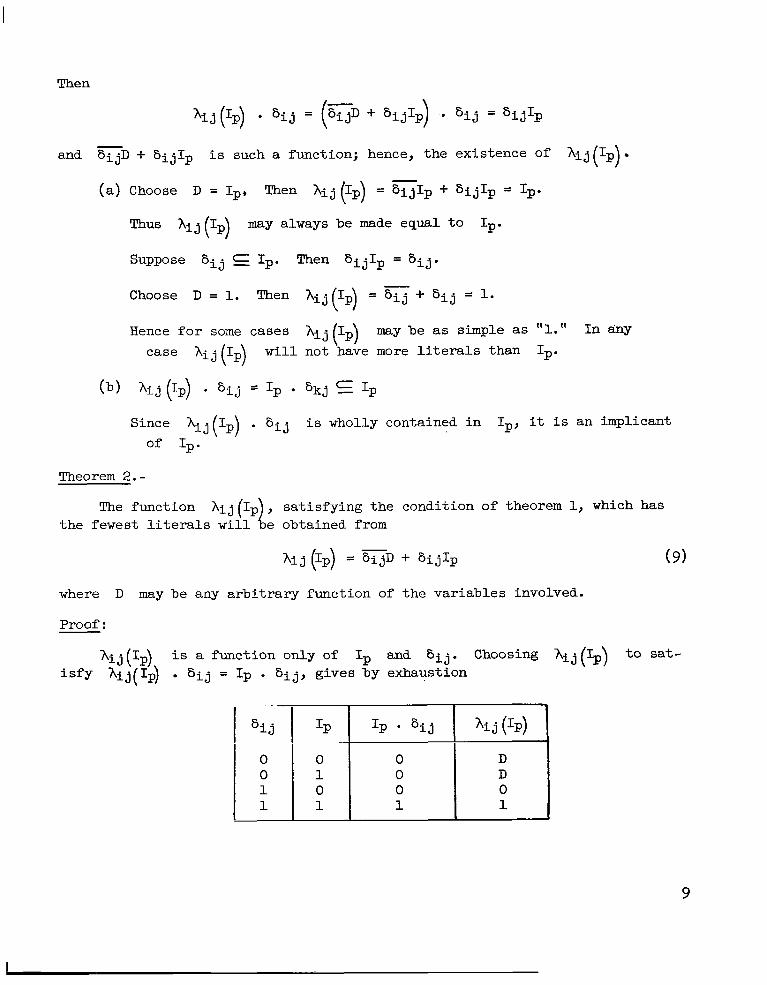
h i j (Ip) i s a function o n l y of Ip and 6 i j . Choosing hi3 (Ip) t o sat- i s f y hij(Ip) 6 i j = IP . 6 i j , gives by exhaustion
9
Hence hij (Ip) = 8ijD + 8ijIp and can be made to have the minimum possible nun- ber of literals since a maximum number of "don't cares" can be included in a map of hij(Ip) in the variables involved.
- fO
f 1
f - 2s-1
MATRIX PROCEDURE
A matrik procedure is now developed which readily permits determination of ability and the simplest solution. a digital computer.
hij(Ip), easily considers redundancies, and allows determination of realiz- The technique is suitable for programing on
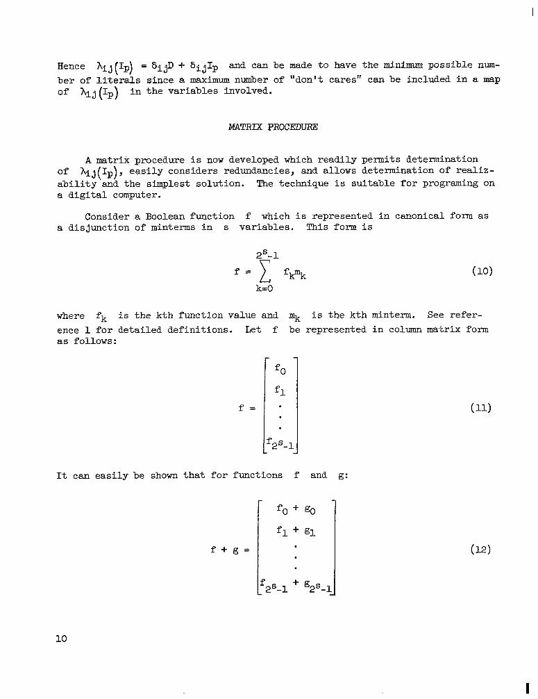
Consider a Boolean function f which is represented in canonical form as a disjunction of minterms in s variables. This form is
where fk is the kth function value and mk is the kth minterm. See refer- ence 1 for detailed definitions. Let f be represented in column matrix form as follows:
It can easily be shown that for functions f and g:
f + g =
+ +
+
10
I
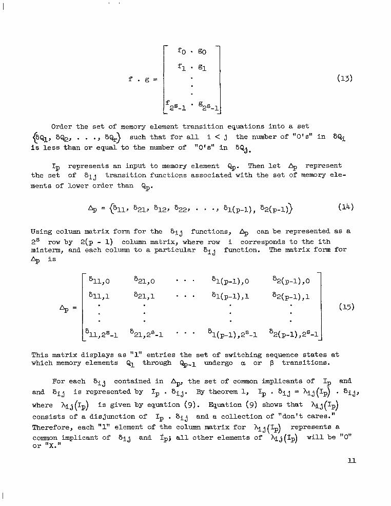
Order the set of memory element transition equations into a set @Ql, E(+, . . ., E%} is less than or equal to the number of
such that for all i < j the number of "0 's ' ' in SQi ' 'O*S" in SQJ
Ip represents an input to memory element %. Then let 4 represent the set of Sij transition functions associated with the set of memory ele- ments of lower order than Qp.
Using column matrix form for the Sij functions, % can be represented as a 2' row by 2(p - 1) column matrix, where row i corresponds to the ith minterm, and each column to a particular Sij function. The matrix form for L$ is
This matrix displays as "1" entries the set of switching sequence states at which memory elements Q1 through &p-l undergo a or p transitions.
For each 6ij contained in Ap, the set of common implicants of Ip and and Sij is represented by Ip . Sij. By theorem 1, Ip . Sij = hij(Ip) . Sij,
is given by equation ( 9 ) . Equation ( 9 ) shows that hi j Ip and a collection of "don't cares."
where hi j (Ip) 0 consists of a disjunction of Therefore, each "1" element of the column matrix for common implicant of Sij and fp; all other elements of hij(1p) will be "0" o r "X."
. 8ij hij (Ip) represents a
11
I I I1 I 1111111111111l11111ll Illl1lIlII11l11111lI
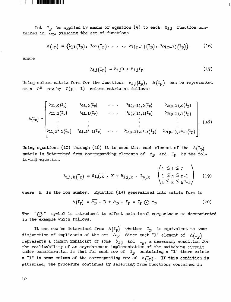
Let Ip be applied by means of equation ( 9 ) to each 6ij function con- tained in Ap, yielding the set of functions
where
Using column matrix form for the functions hij(Ip), A(Ip) can be represented as a 2s row by 2(p - 1) column matrix as follows:
I 1
1 kL,2S-l(Ip) h1,25-1(Ip) * * * h ( p - 1 ) , 2 5 4 Ip) h ( p - 1 ) , 2 5 4 Ip) 1 Using equations (10) through (18) it is seen that each element of the matrix is determined from corresponding elements of Ap and Ip by the fol- lowing equation:
A Ip 0
where k is the row number. Equation (19 ) generalized into matrix form is -
A(Ip) = Ap . D + Ap . Ip = Ip 0 Ap (20)
The "0" in the example which follows.
symbol is introduced to effect notational compactness as demonstrated
It can now be determined from A(1,) whether Ip is equivalent to some disjunction of implicants of the set Ap. Since each "1" element of A(Ip) represents a common implicant of some 6ij and Ip, a necessary condition for the realizability of an asynchronous implementation of the switching circuit under consideration is that for each row of containing a "1" there exists a "1" in some column of the corresponding row of A I . If this condition is satisfied, the procedure continues by selecting from functions contained in
Ip
( P)
12

h(Ip) tion. The subset is then
a minimal subset h'(Ip) which also satisfies the realizability condi-
The set union of the implicants represented by "lis" in the matrix form of h'(Ip) is the complete set of implicants of Ip. Therefore it is seen that
Ip = . "j
Now tjij is associated with an output of memory element Qj which is asserted or negated according to the value of i. The function hij(1p) repre- sents the output of a gating network. P-E input pair of a flip-flop. nus, to implement input I ~ , K(AI(I,))P-E input pairs are necessary, where K(A'(Ip)) A' (Ip). For each P-E pair, an output of Qj (asserted if i = 1 and negated if will feed the E input. hij(Ip), by proper choice of values for its "X" entries, is the simplest function satisfying equation (8) and hence will give the most economical implementation.
The 'I . operation is accomplished by a
is the cardinality of the set
i = 2) will feed the P input and the gating network implementing Aij(Ip) By theorem 2,
If redundant implication of Ip CaMOt be allowed because of the type of flip-flop circuit in use, the process of forming the subset must be modified so that only a single ''1" exists in each row where a "l" is required. This can be readily accomplished by setting redundant ' l l ' s " to "0." The selec- tion of a minimal subset in '̂(Ip) to set to "O", such that the most economical implication of Ip is realized, may be lengthy for cases having large numbers of variables; it would be best carried out by a digital computer.
A1(Ip)
A'(Ip) and the determination of which redundant "1's"
THE ALGORITHM
A step-by-step procedure for synthesis is now given and is followed by an example for clarification.
(1) Determine the switching sequence of the sequential machine.
(2) Make state assignments to the memory elements.
(3) For each memory element Q determine the column matrix of the transi- tion equation SQ. Order the memory element transition equations into a set
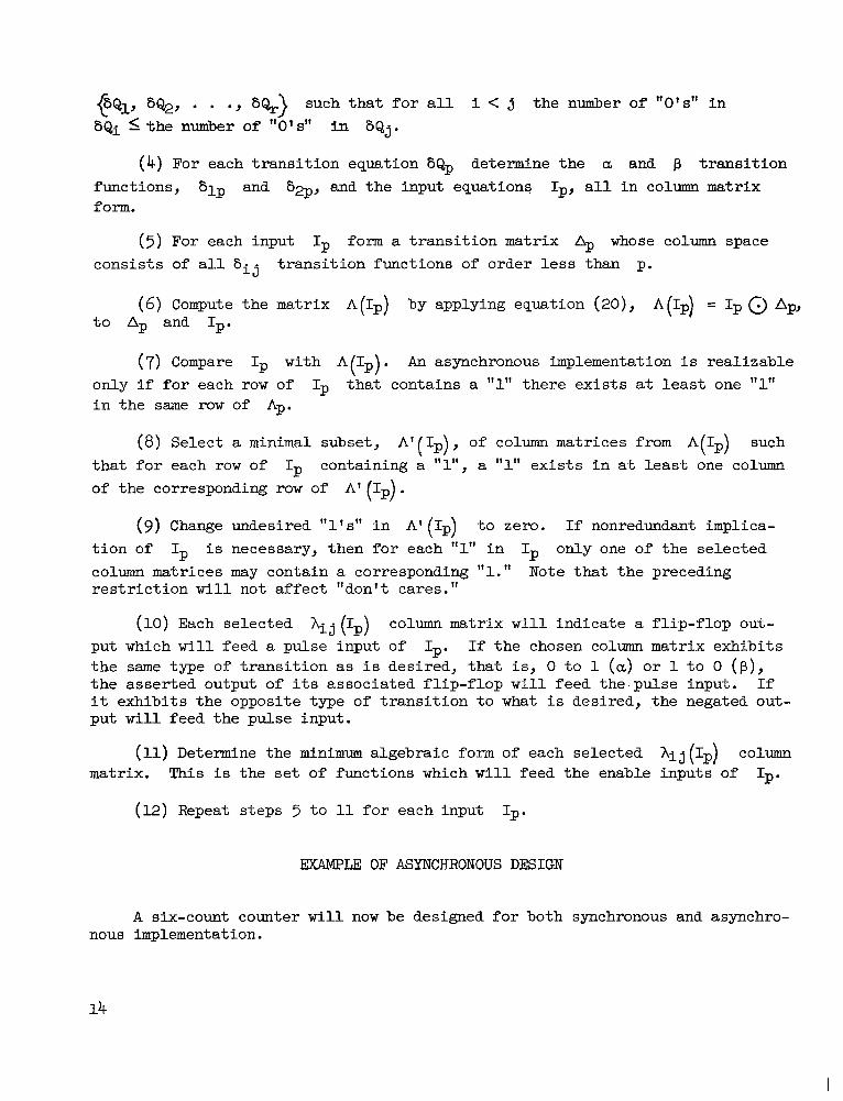
(sq, S%, . . ., Sf&} SQi 5 the number of r r O 1 ~ " in SQj.
such that for all i < j the number of l l O r ~ " in
(4) For each transition equation 8Qp determine the a and p transition functions, 6lp and SzP, and the input equations Ip, all in column matrix f om.
( 5 ) For each input Ip form a transition matrix Ap whose column space consists of all Sij transition functions of order less than p.
(6) Compute the matrix A(Ip) by applying equation (20), A(Ip) = Ip 0 Ap, to Ap and Ip.
(7) Compare Ip with A Ip). An asynchronous implementation is realizable ( only if for each row of in the same row of Ap.
Ip that contains a "1" there exists at least one ''1"
(8) Select a minimal subset, A'(Ip), of column matrices from A(Ip) such containing a "l", a "1" exists in at least one column that for each row of
of the corresponding row of Ip
'̂(Ip).
( 9 ) Change undesired ''1'~~' in A'(Ip) to zero. If nonredundant implica- tion of Ip is necessary, then for each "1" in Ip only one of the selected cob" matrices may contain a corresponding "1." restriction will not affect "don't cares."
Note that the preceding
(10) Each selected hij (Ip) put which will feed a pulse input of Ip. the same type of transition as is desired, that is, 0 to 1 (a) or 1 to 0 (p ) , the asserted output of its associated flip-flop will feed the.pulse input. If it exhibits the opposite type of transition to what is desired, the negated out- put will feed the pulse input.
column matrix will indicate a flip-flop out- If the chosen column matrix exhibits
(11) Determine the minimum algebraic form of each selected Ai j (Ip) column
Ip. matrix. This is the set of functions which will feed the enable inputs of
(12) Repeat steps 5 to 11 for each input Ip.
EXAMPLE OF ASYNCHRONOUS DESIGN
A six-count counter will now be designed for both synchronous and asynchro- nous implementation.

Step 1. The switching sequence is 0, 1, 2, 3, 4, 5, 0, 1, . . . . Step 2. Let flip-flop A3 have a weight of 4, + a weight of 2, and A1 a
weight of 1. The transition table is as follows:
A3n A3"l
0 0 0 1 1 0 X X
are
=
and the transition equations are
6A3 =
. - 0 0 0 a
0 P X X - -
0 1 1 0 1 1 0 0 0 1 0 0 X X X X
Step 3 . The application equations for A3,
6A2 =
0 1 1 0
0 0 X X . .
- - 0
0 P
U
0 0 X X - -
A2, and Ai in column matrix form
Since A1 has the fewest "0 ' s " and since A3 is {~A-J, 6A2, 6A3).
. - a P
P
P X X
a
a
- -
. - 1 0 1 0
1 0 X X - -
(23)
has the most " O ' S ' ~ , the ordering
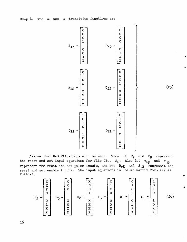
Step 4. The cr, and p t rans i t ion functions a re
612 =
611 =
-
0 0 X - X 1 - 0 1 0 0
0 0 X X - . - 1 0 1 0
1 0 X X , -
623 =
622 =
821 =
0 1 X -7 X
-
0 0 X X - !I - - 0 1 0 1
0 1 X X - -
Assume tha t R-S f l ip - f lops w i l l be used. Then l e t Rp and Sp represent the reset and se t input equations f o r f l ip-f lop Ap. Also l e t -rRP and T~~
represent the reset and s e t pulse inputs, and l e t R p ~ and represent the rese t and s e t enable inputs. The input equations i n column matrix form are a s follows :
0 0
s 3 = [ ; 0
%?=
- . X 0 0 1
X X X X . .
s2 = I] X
X
R 1 = s1 = I!! X
X
f
U
(26 )
16

Note tha t the l a s t two elements of a l l input column matrices a re "X" and corre- spond t o "forbidden" states of the counter. The other ''X's'' resu l t from the f a c t t ha t a f l ip - f lop i n a s e t ( rese t ) s t a t e may be se t ( rese t ) repeatedly without changing i ts s ta te . For synchronous design,-the input equations are therefore R1 = A1, S1 = A1, 5 = b A l , S2 = A3+A1, R 3 = A3A1, and
S3 = A$l.
- - - (See f ig . 3 for a schematic diagram of the synchronous design.)
- X 0 0 1
X X X X d
Step 5. Since A1 i s of lowest order, i t s inputs a re the same as fo r the syn-
3 chronous design. Only A 1 i s properly ordered t o provide pulse inputs t o +. The A2 matrix i s then
0
I, - 1 0 1 0
1 0 X X
0 1 X X 1 -
Step 6. Applying equation (20) t o % and gives
A(%) = R2 04 =
Step 7. Comparing % with the row where % requirements . I
- 1 0 0 1 1 0 0 1
1 0 0 1 X X X X -
X X 0 X
X X X X
X X X # ' I X
b($), it i s seen that bl(%) contains a "1'' i n contains a "l", satisfying the r ea l i zab i l i t y
Step 8. Only b l ( R 2 ) has a "1" corresponding t o the "1" i n R2. Consequently 1
only S21 implies 5, and furthermore it implies @ completely.
Step 9. There are no undesired ''l1s1' i n A21(R2), nor i s redundant implication a problem.
Step 10. Assume tha t pulse inputs respond t o d t ransi t ions. Since 621 exhibits the p t rans i t ion space of A i , the negated output of A 1

must be connected t o the pulse input of
required a, t ransi t ion. The function %1(%) i s the enabling leve l t o feed the enable input of
% i n order t o supply the
+. Step 11. The simplest expression for hl(%) i s 4. Then
I - ~ = A 1 and %E = (29) r
Step 12. Steps .5 through 11 are now repeated f o r input S2. Applying equa- 5
t ion (20) t o S2 and A2 gives
0
0 0 1 0 ]=I 0
1 X X
Since only k1(S2) has a "1" corresponding t o the "1" i n S2, only 621 can imply S2. Then the pulse input I- must be connected t o the negated out- s2 put of A1. The enable input s2E receives the function h1(S2) which i n i t s simplest form i s equal t o A3A2. Then
- -
Both A1 and A;! a re properly ordered t o provide pulse inputs t o A3. Hence A3 becomes
1 1 X
X
0 1 0 1
0 1 X X
0 1 0 0
0 0 X X
C
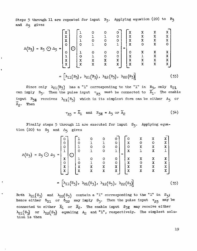
Steps 5 through 11 are repeated f o r input R3. Applying equation (20) t o R 3 and A3 gives
0 1 0 1
0 1 X X
0 1 0 0
0 0 X X
0 X 0
0 0 X X X I-i X X
X X 0
X 1 X X
X X X X
X X X X
X
X X X il X
Since only &(R3) has a "1" corresponding t o the "1" i n R3, only 621 must be connected t o El. The enable
TR3 can imply R3. Then the pulse input
input R3E receives %1(R3) which i n i t s simplest form can be e i ther A3 or &. Then
(34) -
T~~ = A 1 and R ~ E = A 3 Or
Finally steps 5 through 11 are executed f o r input S3. Applying equa- t i o n (20) t o S3 and A3 gives
A(S3) = S3 0 A3 =
1
0 1 X
X
0 1 0 1
0 1 X X
0 1 0 0
0 0 X X
0 0 0
0 0 X X !=I' X
X 0 X 1
X 0 X X
X 0 X X
X X X X
Both $1(S3) and ae(S3) contain a "1" corresponding t o the "1" i n S3; hence e i ther o r 622 may imply S3. Then the pulse input
connected t o e i ther o r &. The enable input s3E may receive e i ther %1('3) Or %2('3) equaling 4 and "1", respectively. The simplest solu- t i o n i s then
may be 753
- T~~ = and S3E = 1
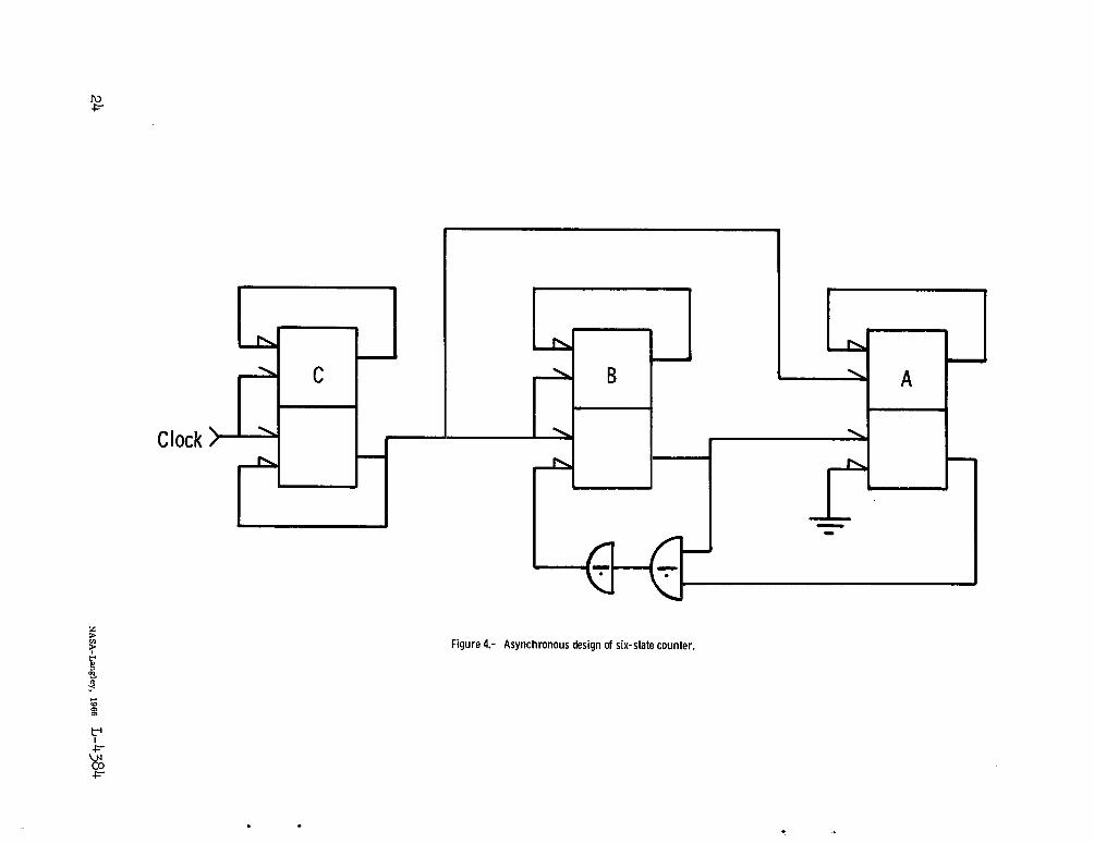
The application of the algorithm is now completed. The asynchronous design Comparing figure 3 with figure 4 shows the increased sim- is shown in figure 4.
plicity achieved by the asynchronous design.
CONCLUDING REMARKS
A formalized algorithm for synthesizing asynchronous sequential circuits has been developed which replaces previous trial and error methods with an organized approach. The algorithm applies to all sequential circuits except those having pulse feedback. an asynchronous implementation for a given sequential circuit and, furthermore, permits determination of the simplest solution if several exist. The matrix method of function representation is readily programable on a digital computer. A computer will be desirable for consideration of cases having a large number of variables.
It permits determination of the realizability of
Langley Research Center, National Aeronautics and Space Administration,
Langley Station, Hampton, Va., September 15, 1965, 125-24-03-03-23.
REFERENCES
1. Phister, Montgomery, Jr.: Logical Design of Digital Computers. John Wiley & Sons, Inc., 1961.
2. [Mergler, H. Wd : Notes on Digital Control Systems Engineering. Vols. 1 and 2, Eng. Div. of Case Inst. Technol.
20

B t
output - Inputs -
- - C-
Sym bo1
Figure 1.- Typical resistance-coupled inverting gate.
21
E P E
Reset \
R E r\
P \
E- P r\
S
0
- 0
P P P E
E P E
Set
Symbol
Figure 2.- Typical ac coupled R-S flip-flop circuit.
22

.
Figure 3.- Synchronous design of six-state counter.
Clock
Figure 4.- Asynchronous design of six-state counter.
.

“The aeronautical and space activities of the United States shall be conducted so as io contribute . . . to the expansion of human knowl- edge of phenomena i j z the atmosphere and space. The Administration shall provide for the widest practicable and appropriate dissemination of information concerning iis activities and the results thereof.”
-NATIONAL AERONAUTICS AND SPACE ACT OF 1958
NASA SCIENTIFIC AND TECHNICAL PUBLICATIONS
TECHNICAL REPORTS: important, complete, and a lasting contribution to existing knowledge.
TECHNICAL NOTES: of importance as a contribution to existing knowledge.
TECHNICAL MEMORANDUMS: Information receiving limited distri- bution because of preliminary data, security classification, or other reasons.
CONTRACTOR REPORTS: Technical information generated in con- nection with a NASA contract or grant and released under NASA auspices.
TECHNICAL TRANSLATIONS: Information published in a foreign language considered to merit NASA distribution in English.
TECHNICAL REPRINTS: Information derived from NASA activities and initially published in the form of journal articles.
SPECIAL PUBLICATIONS: Information derived from or of value to NASA activities but not necessarily reporting the results ,of individual NASA-programmed scientific efforts. Publications include conference proceedings, monographs, data compilations, handbooks, sourcebooks, and special bibliographies.
Scientific and technical information considered
Information less broad in scope but nevertheless
Details on the availability of these publications may be obtained from:
,
SCIENTIFIC AND TECHNICAL INFORMATION DIVISION
NATIONAL AERONAUTICS AND SPACE ADMINISTRATION
Washington, D.C. PO546