high level synthesis of mean shift tracking algorithm · high level synthesis of mean-shift...
TRANSCRIPT

i
High Level Synthesis of Mean-Shift Tracking
Algorithm
By
Ahmed Kamal El-Din Ahmed El-Sayed
Islam Mohamed Abd El-Gawad
Islam Samir Mohamed Ahmed
Islam Osama Ahmed Mounir
Khaled Magdy Ghanem
A Graduation Project Report Submitted to
the Faculty of Engineering at Cairo University
in Partial Fulfillment of the Requirements for the
Degree of
Bachelor of Science
in
Electronics and Communications Engineering
Faculty of Engineering, Cairo University
Giza, Egypt
July 2012
ii
Table of Contents
List of Figures .............................................................................................................. vii
List of Tables ................................................................................................................ ix
List of Symbols and Abbreviations................................................................................ x
Acknowledgments......................................................................................................... xi
Abstract ........................................................................................................................ xii
Chapter 1: High Level Synthesis ............................................................................... 1
1.1 The need for design automation on higher abstraction levels ......................... 1
1.2 Levels of Abstraction ...................................................................................... 3
1.3 Definition of Synthesis .................................................................................... 4
1.4 High level synthesis algorithms ...................................................................... 6
1.4.1 Partitioning ............................................................................................... 7
1.4.2 Scheduling................................................................................................ 8
1.4.3 Allocation ............................................................................................... 13
Chapter 2: Catapult C Synthesis .............................................................................. 18
2.1 Introduction ................................................................................................... 18
2.2 Benefits of Using Automated HLS ............................................................... 19
2.2.1 Reducing Design and Verification Efforts ............................................. 19
2.2.2 More Effective Reuse ............................................................................ 19
2.2.3 Investing R&D Resources Where it really Matters ............................... 20
2.2.4 Seizing the Opportunity ......................................................................... 20
2.3 How HLS is done by Catapult? ..................................................................... 21
2.3.1 Generating the DFG from the input untimed C++ code ........................ 21
2.3.2 Resource Allocation ............................................................................... 21
2.3.3 Scheduling.............................................................................................. 22
2.3.4 Loops...................................................................................................... 23
2.4 Design process............................................................................................... 26

iii
2.4.1 Step 1: Writing and Testing the C Code ................................................ 27
2.4.2 Step 2: Analyzing the Algorithm ........................................................... 27
2.4.3 Step 3: Creating the Hardware Design................................................... 32
2.4.4 Step 4: Performing Timed Simulation ................................................... 32
2.4.5 Step 5: Synthesizing the RTL design ..................................................... 33
2.5 Design Example ―FIR‖.................................................................................. 33
2.5.1 C++ Code ............................................................................................... 33
2.5.2 Setup Design .......................................................................................... 33
2.5.3 Architecture Constraints ........................................................................ 34
2.5.4 Results .................................................................................................... 35
Chapter 3: Object Tracking Using Mean-Shift Algorithm ...................................... 37
3.1 Introduction ................................................................................................... 37
3.2 Object Representation ................................................................................... 38
3.2.1 Object Shape Representation ................................................................. 38
3.2.2 Object Appearance Representation ........................................................ 40
3.3 Feature Selection for Tracking ...................................................................... 41
3.4 Mean-Shift Algorithm for Object Tracking .................................................. 42
3.4.1 Target Model .......................................................................................... 42
3.4.2 Target Candidate Model ........................................................................ 43
3.4.3 Similarity Function ................................................................................ 43
3.4.4 Target Localization ................................................................................ 44
3.5 Modifications on the Mean-Shift Algorithm ................................................. 46
3.5.1 Epanechnikov Kernel Calculation ......................................................... 46
3.5.2 Weights Calculation ............................................................................... 47
3.6 Developing the Algorithm for Colored Object Tracking .............................. 47
3.6.1 HSV representation ................................................................................ 47
3.6.2 RGB to HSV transformation:................................................................. 48

iv
3.6.3 Color space transformation module(Block): .......................................... 50
Chapter 4: Design Implementation .......................................................................... 52
4.1 Developing Floating Point MATLAB Model ............................................... 53
4.2 Developing the Floating Point C Model ....................................................... 53
4.3 Developing the Fixed Point C Model ............................................................ 54
4.4 HLS Using Catapult C Synthesis Tool .......................................................... 54
4.5 Functional Simulation Using ModelSim ....................................................... 55
4.6 Logic Synthesis Using Precision RTL .......................................................... 55
4.7 Place and Route using Quartus II .................................................................. 56
4.8 Results and Conclusions................................................................................ 56
4.9 Calculated Results ......................................................................................... 56
4.10 Conclusions ............................................................................................... 57
Chapter 5: Testing &Verification ............................................................................ 58
5.1 Introduction ................................................................................................... 58
5.1.1 Formal Verification ................................................................................ 58
5.1.2 Functional Verification Approaches ...................................................... 59
5.2 Testing VS Verification ................................................................................ 60
5.3 Software Verification Flow for Mean-Shift Algorithm ................................ 60
5.3.1 Testing the Functionality of the Fixed-Point C Model .......................... 60
5.4 Hardware verification flow ........................................................................... 62
5.4.1 Functional Verification Using System C Testbench .............................. 62
5.4.2 The SCVerify Flow (SystemC Verify Flow) ......................................... 62
5.4.3 Traditional VHDL testbench .................................................................. 65
5.5 Timing Analysis ............................................................................................ 66
5.5.1 Static Timing Analysis ........................................................................... 66
5.5.2 Dynamic timing analysis........................................................................ 69
Chapter 6: Hardware Implementation and Results .................................................. 71
v
6.1 FPGA Overview ............................................................................................ 71
6.2 Advantages of FPGA design Methodologies ................................................ 71
6.2.1 Early Time to Market ............................................................................. 72
6.2.2 IP Integration ......................................................................................... 72
6.2.3 Tool Support .......................................................................................... 72
6.2.4 Transition to structured ASICs .............................................................. 73
6.3 Embedded System Design ............................................................................. 73
6.3.1 SOPC Builder Design ............................................................................ 75
6.3.2 Software Design ..................................................................................... 76
6.4 Cyclone III EP3C25 NIOS II Starter Kit ...................................................... 77
6.4.1 The Main Features of the Cyclone III Starter board: ............................. 78
6.4.2 Main Advantages of the Cyclone III Starter Board ............................... 79
6.4.3 Board Component Blocks ...................................................................... 79
6.5 NIOS II Overview ......................................................................................... 81
6.5.1 Introduction ............................................................................................ 81
6.5.2 Register File and ALU ........................................................................... 84
6.5.3 Memory and I/O Organization ............................................................... 85
6.5.4 Exception and Interrupt Handler ............................................................ 89
6.5.5 JTAG Debug Module ............................................................................. 89
6.6 NIOS II in Video Processing ......................................................................... 90
6.6.1 Working Demo Procedure ..................................................................... 90
6.6.2 System Overall Block Diagram ............................................................. 91
6.6.3 Flow Summary from Quartus ................................................................ 91
References .................................................................................................................... 93
Appendix A: Software verification using Visual C ..................................................... 94
Appendix B: SCVerify setting Steps ........................................................................... 96
Step 1: Prepare a New Project ............................................................................. 96

vi
Step 2: Design Configuring the Setup Options .................................................... 96
Step 3: Augment the Original Testbench for SCVerify Flow .............................. 96
Step 4: Generate Verification Output Files .......................................................... 97
Step 5: Launch Simulation from Makefile ........................................................... 99
Elements of the Testbench ................................................................................... 99
Appendix C: Nios II 10.0 software build tool for Eclipse ......................................... 103
vii
List of Figures
Figure 1-1: Gajski Y-chart ............................................................................................. 3
Figure 1-2: High Level Synthesis .................................................................................. 6
Figure 1-3: Clustering Operations ................................................................................. 7
Figure 1-4: Behavioral description decomposition ........................................................ 8
Figure 1-5: a) DFG of a simple algorithm, b) Scheduling of this DFG ......................... 9
Figure 1-6: Classification of scheduling algorithms .................................................... 10
Figure 1-7: ASAP algorithm ........................................................................................ 11
Figure 1-8: ALAP algorithm ........................................................................................ 11
Figure 1-9: DFG of the IIR Filter ................................................................................ 12
Figure 1-10: ASAP schedule ....................................................................................... 12
Figure 1-11: ALAP schedule with maximum latency constrained to 5 cycles ............ 13
Figure 1-12: ALAP schedule with maximum latency constrained to 5 cycles ............ 15
Figure 1-13: Allocation of above DFG ........................................................................ 15
Figure 2-1: Data flow graph description ...................................................................... 21
Figure 2-2: Resource Allocation .................................................................................. 22
Figure 2-3: Scheduling design ..................................................................................... 22
Figure 2-4: Datapath State Diagram ............................................................................ 23
Figure 2-5: Schedule for accumulate using loops ........................................................ 24
Figure 2-6: Schedule for Accumulate Unrolling by 2 ................................................. 25
Figure 2-7: Schedule for accumulate fully loop unrolling ........................................... 25
Figure 2-8: Catapult Synthesis Flow............................................................................ 26
Figure 2-9: Catapult Interface Control Section ............................................................ 29
Figure 2-10: Input output settings ................................................................................ 30
Figure 2-11: Catapult loop iteration constraint ............................................................ 30
Figure 2-12: Catapult resource constraint .................................................................... 31
Figure 2-13: Catapult Schedule Window ..................................................................... 32
Figure 2-14: Area scores .............................................................................................. 35
Figure 2-15: Timing scores .......................................................................................... 36
Figure 3-1: Object shape representations. .................................................................... 39
Figure 3-2: Multi-views of a car. ................................................................................. 40
Figure 3-3: a) 2-D Epanechnikov Kernel b) 3-D Epanechnikov Kernel ................... 43
Figure 3-4: Complete flowchart of Mean-Shift tracking algorithm ............................. 45
viii
Figure 3-5: Object is two frames ................................................................................. 46
Figure 3-6: The HSV Cone .......................................................................................... 48
Figure 3-7: RGB cube representation .......................................................................... 48
Figure 4-1: Design Procedure ...................................................................................... 52
Figure 5-1: Testing versus verification ........................................................................ 60
Figure 5-2: Software Verification Flow ....................................................................... 61
Figure 5-3: System C is used to reduce the verification effort .................................... 62
Figure 5-4 Generalized Test Infrastructure .................................................................. 63
Figure 5-5: SCVerify flow diagram ............................................................................. 64
Figure 5-6: Structure of a testbench with reusable bus functional model .................... 65
Figure 5-7: Structure of a test bench with reusable utility routines ............................. 66
Figure 5-8: STA ........................................................................................................... 67
Figure 5-9: Timing analysis and verification (in design flow) .................................... 70
Figure 6-1: Embedded System Design Flow ............................................................... 74
Figure 6-2 Cyclone III FPGA Starter Kit .................................................................... 78
Figure 6-3: Cyclone III FPGA Starter blocks .............................................................. 79
Figure 6-4: The conceptual block diagram of a Nios II processor .............................. 83
Figure 6-5: NIOS II internal Architecture ................................................................... 86
Figure 6-6: Overall system block diagram................................................................... 91

ix
List of Tables
Table 2-1: Design Constraint ....................................................................................... 34
Table 2-2: Performance parameters for different designs............................................ 35
Table 5-1: Specifications of the three different implementations of the Mean Shift
Tracker ......................................................................................................................... 56
Table 5-2: Comparison results ..................................................................................... 56
Table 6-1: Comparison between NIOS II three basic versions.................................... 84
Table 6-2: Video and Image Processing Suite IP MegaCore Functions ...................... 90

x
List of Symbols and Abbreviations
CAD Computer Aided Design
VLSI Very Large Scale Integrated circuits
RTL Register Transfer Level
RAM Random Access Memory
ROM Read Only Memory
HLS High Level Synthesis
DFG Data Flow Graph
CDFG Control/Data Flow Graph
FSMD Finite State Machine with a Datapath
C-step Control step
ASAP As Soon As Possible
ALAP As Late As Possible
FPGA Field Programmable Gate Array
DSP Digital Signal Processing
MS Mean-Shift
ATPG Automatic Test Pattern Generation
MCMs Multi-Chip Module
ASIC Application Specified Integrated Circut

xi
Acknowledgments
The authors wish to express their gratitude to their supervisor, Prof. Dr.Serag El-din
Habib who was abundantly helpful and offered invaluable assistance, support and
guidance. Deepest gratitude is also due to Eng.Ahmed Abd-Eltawab for his great
assistance to us.

xii
Abstract
Over the last couple decades, progress in logic synthesis techniques effectively moved
the description of logic circuits from the logic level up to the Register transfer level
(RTL). Now, hardware description languages (e.g. VHDL) are routinely used to enter
the digital circuit designs. The next step is to move the design entry up to the
algorithm level. Current progress in High Level Synthesis (HLS) techniques enabled
the introduction of CAD tools that help the designer map algorithms ( in C or C++
form) to RTL. These HLS tools are enable breakthrough gains in design time,
designer productivity, design space exploration and verification. The objective of this
project is to design an object tracker, as a relatively complex digital circuit, using
HLS techniques. The widely used Mean Shift (MS) object tracking algorithm is
adopted. Mentor Graphics‘ Catapult HLS tool is utilized. The design starts with a
MATLAB code of the MS algorithm. Next, we map this algorithm to a fixed point C-
model suitable for Catapult tool. Then, the tool generates the corresponding data flow
graph and carries out the scheduling step according to the speed and area constraints.
The generated VHDL output is verified for correct functional behavior. Next, this
design is mapped to logic level, targeting an FPGA platform.

1
High Level Synthesis Chapter 1:
1.1 The need for design automation on higher abstraction levels
VLSI technology reached densities of over one million transistors of random logic per chip in
the early 1990s. Systems of such complexity are very difficult to design by handcrafting each
transistor or by defining each signal in terms of logic gates. As the complexities of systems
increase, so will the need for design automation on more abstract levels where functionality
and tradeoffs are easier to understand.
VLSI technology has also reached a maturity level; it is well understood and no longer
provides a competitive edge by itself. The industry has started looking at the product
development cycle comprehensively to increase productivity and to gain a competitive edge.
Automation of the entire design process from conceptualization to silicon has become a
necessary goal in the 1990s.
The concepts of first silicon and first specification both help to shorten the time-to-market
cycle. Since each iteration through the fabrication line is expensive, the first- silicon approach
works to reduce the number of iterations through the fabrication line to only one. This
approach requires CAD tools for verification of both functionality and design rules for the
entire chip. Since changes in specification may affect the entire team, the first-specification
approach has a goal of reducing the number of iterations over the product specification to
only one. A single –iteration specification methodology requires accurate modeling of the
design process and accurate estimation of the product quality measures, including
performance and cost. Furthermore, these estimates are required early in the product
specification phase.
There are several advantages to automating a part of all of the design process and moving
automation to higher levels. First, automation assures a much shorter design cycle. Second, it
allows for more exploration of different design styles since different designs can be generated
and evaluated quickly. Finally, if synthesis algorithms are well understood, design
automation tools may out-perform average human designers in generating high quality
designs. However, correctness verification of these algorithms and of CAD tools in general,
is not easy. CAD tools still cannot match human quality in automation of the entire design
process, although human quality can be achieved on a single task. The two main obstacles are

2
a large problem size that requires very efficient search of the design space and a detailed
design model that requires sophisticated algorithms capable of satisfying multiple constraints.
Two schools of thought emerged from the controversy over solutions to these two problems.
The capture-and-simulation school believes that human designers have very good design
knowledge accumulated through experience that cannot be automated. This school believes
that a designer builds a design hierarchy in a bottom up fashion from elementary components
such as transistors and gates. Thus, design automation should provide CAD tools that capture
various aspects of design and verify them predominantly through simulation. This approach
focuses on a common framework that integrates capture-and-simulation tools for different
levels of abstraction and allows designers to move easily between different levels.
The describe-and-synthesize believes that synthesis algorithms can out-perform human
designers. Subscribers to this approach assume that human designers optimize a small
number of objects well, but are not capable of finding an optimal design when thousands of
objects are in question. CAD algorithms search the design space more thoroughly and are
capable of finding nearly optimal designs. This school believes that a top down methodology,
in which designers describe the intent of the design and CAD tools add detailed physical and
electrical structure, would be better suited for the future design of complex systems. This
approach focuses on definition of description languages, design models, synthesis algorithms
and environments for interactive synthesis in which designer‘s intuition can substantially
reduce the search through the design space.
Both these schools of thought may be correct at some point during the evolution of the
technology. For example, it is still profitable to handcraft a memory cell that is replicated
millions of times. On the other hands, optimizing a 20,000 date design while using a gate-
array with 100,000 gates is not cost effective if the design already satisfies all other
constraints. Thus, at this point in technological evolution, even suboptimal synthesis becomes
more cost effective than design handcrafting. We believe that VLSI technology has reached
the point where high-level synthesis of VLSI chips and electronic systems is becoming cost
effective.

3
1.2 Levels of Abstraction
We define design synthesis, as a translation process from a behavioral description into a
structural description. To define and differentiate types of synthesis, we use the Gajski Y-
chart in Figure 1-1.
In the behavioral domain we are interested in what a design does, not in how it is built. We
treat the design as one or more black boxes with a specified set of inputs and outputs and a
set of functions describing the behavior of each output in terms of the inputs over time. In
addition to stating functionality, a behavioral description includes an interface description of
constraints imposed on the design. The interface description specifies the I/O ports and
timing relationships or protocols among signals at those ports. Constraints specify
technological relationships that must hold for the design to be verifiable, testable,
manufacturable and maintainable.
To describe behavior, we use transfer functions and timing diagrams on the circuit level and
Boolean expressions and state diagrams on the logic level. On the RTL level, time is divided
into intervals called control states or steps. We use a register-transfer description, which
Figure 1-1: Gajski Y-chart

4
specifies for each for control states the condition to be tested, all register transfers to be
executed, and the next control to be entered. On the system level, we use variables and
language operators to express functionality of system components. Variables and data
structures are not bound to registers and memories, and operations are not bound to any
functional units or control states. In a system level description, timing is further abstracted to
the order in which variable assignments are executed.
A structural representation bridges the behavioral and physical representation. It is a one-to-
many mapping of a behavioral representation onto a set of components and connections
under constraints such as cost, area and delay. At times, a structural representation such as a
logic or circuit schematic may serve as a functional description. On the other hand,
behavioral descriptions such as Boolean expressions suggest a trivial implementation, such as
sum of product structure consisting of NOT, AND and OR gates. On the circuit level, the
basic elements are transistors, resistors, and capacitors, while gates and flip-flops are the
basic elements on the logic level. ALUs, multipliers, registers, RAMs and ROMs are the used
to identify register-transfers. Processors, memories and buses are used on the system level.
The physical representation ignores, as much as possible, what the design is supposed to do
and binds its structure in space or to silicon. The most commonly used levels in the physical
representation are polygons, floorplans, multi-chip modules (MCMs) and printed circuit (PC)
boards.
1.3 Definition of Synthesis
We define synthesis as a translation from behavioral description into structural description
(Figure 1-1), similar to the compilation of programming languages as C into an assembly
language. Each component in the structural description is in turn defined by its own
behavioral description. The component structure can be obtained through synthesis on a
lower abstraction level. Synthesis, sometimes called design refinement, adds an additional
level of detail that provides information needed for the next level of synthesis or for
manufacturing of the design. This more detailed design must satisfy design constraints
supplied with the original description or generated by a previous synthesis step.
Each synthesis step may differ in sophistication, since the work involved is proportional to
the difference in the amount of information between the behavioral description and the
synthesized structural descriptions. For example, a sum-of-products Boolean expression can

5
be trivially converted into a 2-level AND-OR implementation using AND and OR gates with
an unlimited number of inputs. Substantially more work is needed to implement the same
expression with only 2-input NAND gates. Although each behavioral description may
suggest some trivial implementations, it is generally impossible to find an optimal
implementation under arbitrary constraints for an arbitrary library of components.
We will now briefly describe the synthesis tasks at each level of the design process. Circuit
synthesis generates a transistor schematic from a set of input-output current, voltage, and
frequency characteristics or equations. The synthesized transistor schematic contains
transistor types, parameters and sizes.
Logic synthesis translates Boolean expressions into a netlist of components from a given
library of logic gates such as NAND, NOR, XOR, and AND-OR-INVERT. In many cases, a
structural description using one library must be converted into one using another library. To
do so we convert the first structural description into Boolean expressions, and then
resynthesize it using the second library.
Register-transfer synthesis starts with a set of states and a set of register-transfers in each
state. One state corresponds roughly to a clock cycle. Register-transfer synthesis generates
the corresponding structure in two parts:
Datapath, which is a structure of storage elements and functional units that performs
the given register transfers
Control unit, which controls the sequencing of the states in the register-transfer
description.
System synthesis starts with a set of processes communicating through either shared variables
or message passing. It generates a structure of processors, memories, controllers and interface
adapters from a set of system components. Each component can be described by a register-
transfer description.
High level synthesis is the process of generating a structural implementation at register
transfer level (RTL) description of: [ALU‘s, REG‘s, MUX‘s] and controller, which
corresponds to the behavioral specification at system level (algorithm) of a certain design as
shown in Figure 1-2.

6
The synthesis tasks previously described generate structures that are not bound in physical
space. At each level of the design, we need another phase of synthesis to add physical
information. For example, physical design or layout synthesis translates a structural
description into layout information ready for mask generation. Cell synthesis generates a cell
layout from a given transistor schematic with specified transistor sizes. Gate netlists are
converted into modules by placing cells into several rows and connecting I/O pins through
routing in the channels between the cells. Microarchitecture is converted onto chip layout
through floorplanning with modules that represent register-transfer components. Systems are
usually obtained by placing chips on multi-chip carriers or printed circuit boards and
connecting them through several layers of interconnect.
1.4 High level synthesis algorithms
As we defined earlier, synthesis is a transformation of a behavioral description into a set of
connected storage and functional units. General types of algorithms used in HLS are
partitioning, scheduling and allocation. In this section, we will illustrate these algorithms and
how it is used.
Figure 1-2: High Level Synthesis
7
1.4.1 Partitioning
In the context of computer-aided design, partitioning is the task of clustering objects into
groups so that a given objective function is optimized with respect to a set of design
constraints. Partitioning has been used frequently in physical design. For example, it is often
used at the layout level to find strongly connected components that can be placed together in
order to minimize the layout area and propagation delay. It can also be used to divide a large
design into several chips to satisfy packaging constraints.
Partitioning is used in HLS for scheduling, allocation, unit selection and chip and system
partitioning.
First, partitioning can be used to cluster variables and operations into groups so that each
group is mapped into a storage element, a functional unit or an interconnection unit for the
real design. The result of this partitioning can be used for unit selection before scheduling and
binding or it can be used for allocation. It is particularly useful in unit selection since the sum
of all unit areas gives a rough estimate of the chip area. Similarly, partitioning can be used to
cluster operations into groups so that each group is executed in the same control state or
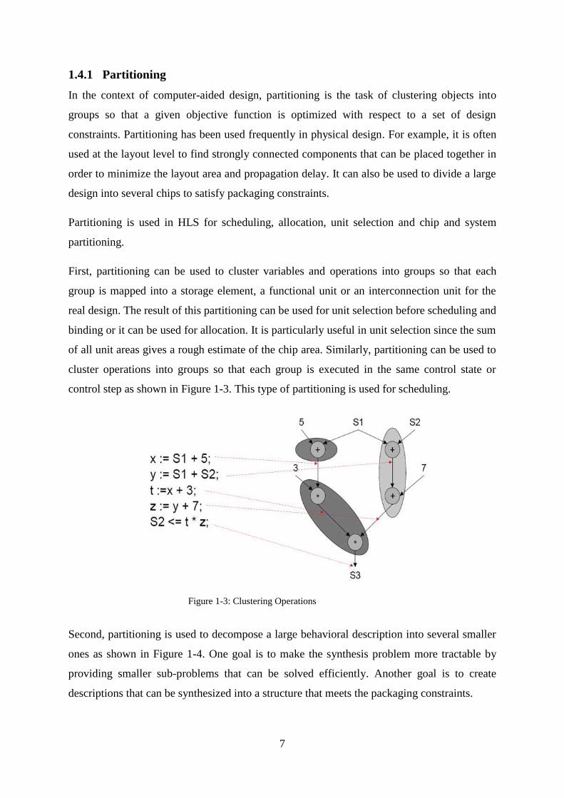
control step as shown in Figure 1-3. This type of partitioning is used for scheduling.
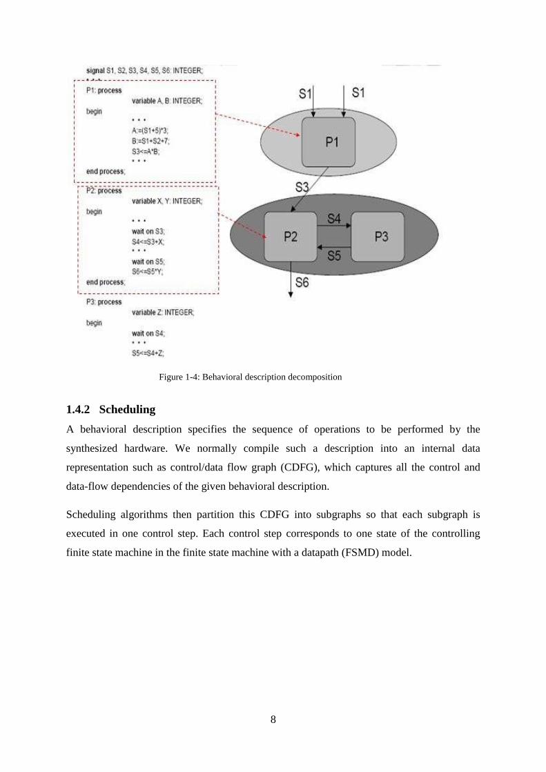
Second, partitioning is used to decompose a large behavioral description into several smaller
ones as shown in Figure 1-4. One goal is to make the synthesis problem more tractable by
providing smaller sub-problems that can be solved efficiently. Another goal is to create
descriptions that can be synthesized into a structure that meets the packaging constraints.
Figure 1-3: Clustering Operations
8
1.4.2 Scheduling
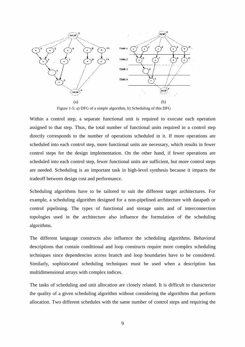
A behavioral description specifies the sequence of operations to be performed by the
synthesized hardware. We normally compile such a description into an internal data
representation such as control/data flow graph (CDFG), which captures all the control and
data-flow dependencies of the given behavioral description.
Scheduling algorithms then partition this CDFG into subgraphs so that each subgraph is
executed in one control step. Each control step corresponds to one state of the controlling
finite state machine in the finite state machine with a datapath (FSMD) model.
Figure 1-4: Behavioral description decomposition
9
Within a control step, a separate functional unit is required to execute each operation
assigned to that step. Thus, the total number of functional units required in a control step
directly corresponds to the number of operations scheduled in it. If more operations are
scheduled into each control step, more functional units are necessary, which results in fewer
control steps for the design implementation. On the other hand, if fewer operations are
scheduled into each control step, fewer functional units are sufficient, but more control steps
are needed. Scheduling is an important task in high-level synthesis because it impacts the
tradeoff between design cost and performance.
Scheduling algorithms have to be tailored to suit the different target architectures. For
example, a scheduling algorithm designed for a non-pipelined architecture with datapath or
control pipelining. The types of functional and storage units and of interconnection
topologies used in the architecture also influence the formulation of the scheduling
algorithms.
The different language constructs also influence the scheduling algorithms. Behavioral
descriptions that contain conditional and loop constructs require more complex scheduling
techniques since dependencies across branch and loop boundaries have to be considered.
Similarly, sophisticated scheduling techniques must be used when a description has
multidimensional arrays with complex indices.
The tasks of scheduling and unit allocation are closely related. It is difficult to characterize
the quality of a given scheduling algorithm without considering the algorithms that perform
allocation. Two different schedules with the same number of control steps and requiring the
Figure 1-5: a) DFG of a simple algorithm, b) Scheduling of this DFG
(a) (b)
10
same number of functional units may result in designs with substantially different quality
metrics after allocation is performed.
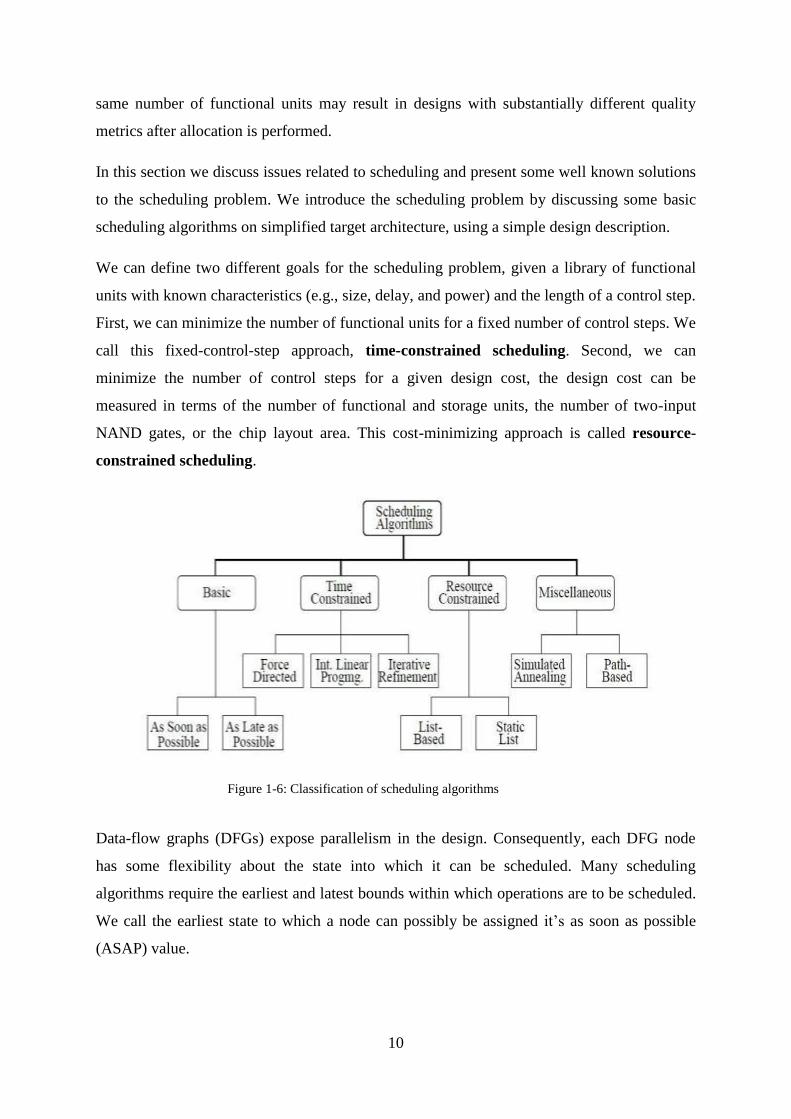
In this section we discuss issues related to scheduling and present some well known solutions
to the scheduling problem. We introduce the scheduling problem by discussing some basic
scheduling algorithms on simplified target architecture, using a simple design description.
We can define two different goals for the scheduling problem, given a library of functional
units with known characteristics (e.g., size, delay, and power) and the length of a control step.
First, we can minimize the number of functional units for a fixed number of control steps. We
call this fixed-control-step approach, time-constrained scheduling. Second, we can
minimize the number of control steps for a given design cost, the design cost can be
measured in terms of the number of functional and storage units, the number of two-input
NAND gates, or the chip layout area. This cost-minimizing approach is called resource-
constrained scheduling.
Data-flow graphs (DFGs) expose parallelism in the design. Consequently, each DFG node
has some flexibility about the state into which it can be scheduled. Many scheduling
algorithms require the earliest and latest bounds within which operations are to be scheduled.
We call the earliest state to which a node can possibly be assigned it‘s as soon as possible
(ASAP) value.
Figure 1-6: Classification of scheduling algorithms

11
The as late as possible (ALAP) value for a node defines the latest state to which a node can
possibly be scheduled. Given a time constraint of T control steps, the algorithm determines
the latest possible control step in which an operation must begin execution. The ASAP and
ALAP scheduling algorithms could be performed by defining the set of all immediate
successors and predecessors of each node.
The ASAP scheduling algorithm could be executed as shown in Figure 1-2.
Where vi is the operation to be scheduled, τ(vi) is the start point of the operation vi, (vi,vj) ∈ E
means that vj is the successor of vi, di is the duration of the vi operation.
Also, the ALAP scheduling algorithm could be executed as shown in Figure 1-3.
Figure 1-7: ASAP algorithm
Figure 1-8: ALAP algorithm

12
Where Lmax is the maximum latency of the whole process.
Consider the following example of a simple IIR Filter,
( ) ( ) ( )
( ) ( ) ( ) ( ) ( )
Then, the DFG is shown in the following figure (Figure 1-4).
Then, the ASAP and ALAP schedules are shown in Figure (1-4) and Figure (1-5)
respectively.
Figure 1-9: DFG of the IIR Filter
Figure 1-10: ASAP schedule

13
1.4.3 Allocation
As described above, scheduling assigns operations to control steps and thus converts a
behavioral description into a set of register transfers that can be described by a state table. A
target architecture for such description in the FSMD from the control-step sequence and the
conditions used to determine the next control step in the sequence. The datapath is derived
from the register transfers assigned to each control step; this task is called datapath synthesis
or datapath allocation.
A datapath in the FSMD model is a netlist composed of three types of register transfer (RT)
components or units: functional, storage and connection. Functional units, such as adders,
shifters, ALUs, and multipliers, execute the operations specified in the behavioral
description. Storage units, such as registers, register files, RAMs, and ROMs, hold the values
of variables generated and consumed during the execution of the behavior. Interconnection
units, such buses and multiplexers, transport data between the functional and storage units.
Datapath allocation consists of two essential tasks: unit selection and unit binding. Unit
selection determines the number and types of RT components to be used in the design. Unit
binding involves the mapping of the variables and operations in the scheduled CDFG into the
functional, storage and interconnection units, while ensuring that the design behavior
operates correctly on the selected set of components. For every operation in the CDFG, we
need variable that is across several control steps in the scheduled CDFG, we need a storage
unit to hold the data values during the variable‘s lifetime. Finally, for every data transfer in
Figure 1-11: ALAP schedule with maximum latency constrained to 5 cycles

14
the CDFG, we need a set of interconnection units to affect the transfer. Besides the design
constraints, imposed on the original behavior and represented in the CDFG, additional
constraints on the binding process are imposed by the type of the hardware units selected. For
example, a functional unit can execute only one operation in any given control step.
Similarly, the number of multiple accesses to a storage unit during a control step is limited by
the number of parallel ports of the unit.
We illustrate the mapping of variables and operations in the DFG of Figure 1-6 into RT
components. Let us assume that we select two adders ADD1 and ADD2 and four registers r1,
r2, r3, and r4. Operations O1 and O2 cannot be mapped in the same control step S1. On the
other hand, operation O1 can share the adder with operation O3 because they are carried out
during different control steps. Thus, operations O1 and O3 are both mapped into ADD1.
Variables a and e must be stored separately because their values are needed concurrently in
control step S2. Registers r1 and r2, where variables a and e reside, must be connected to the
input ports of ADD1; otherwise, operation O3 will not be able to execute in ADD!. Similarly,
operations O2 and O4 are mapped to ADD2. Note that, there are several different ways of
performing the binding. For example, we can map O2 and O3 to ADD1 and O1 and O4 to
ADD2. The allocation is shown in Figure 1-7.
Besides implementing the correct behavior, the allocated datapath must meet the overall
design constraints in area, delay, and power dissipation. To simplify the allocation problem,
we use two quality measures for the datapath allocation: the total size of the design (i.e. the
silicon area in case of ASIC or number of logic elements in case of FPGA platform) and the
worst case register-to-register delay (i.e. the clock cycle) of the design.
We can solve the allocation problem in three ways: greedy approaches, which progressively
construct a design while traversing the CDFG; decomposition approaches, which decompose
the allocation problem into its constituent parts and solve each of them separately; and
iterative methods, which try to combine and interleave the solution of the allocation
problems.

15
Allocation Tasks 1.4.3.1
Datapath synthesis consists of four different interdependent tasks: module selection,
functional-unit allocation, storage allocation and interconnection allocation. In this section,
we define each task and discuss the nature of their interdependence
1.4.3.1.1 Unit Selection
A simple design model may assume that we have only one particular type of functional unit
for each behavior operation. However, a real RT component library contains multiple types
of functional units, each with different characteristics (e.g. functionality, size, delay, and
power dissipation) and each implementing one or several different operations in the register-
transfer description. For example, an addition can be carried out by either a small but slow
Figure 1-12: ALAP schedule with maximum latency constrained to 5 cycles
Figure 1-13: Allocation of above DFG
F

16
ripple adder or by a large but fast carry look-ahead adder. Furthermore, we can use several
different component types, such as an adder, an adder/subtractor or an entire ALU, to
perform an addition operation. Thus, unit selection selects the number and types of different
functional and storage units from the component library. A basic requirement for unit
selection is that the number of units performing a certain type of operation must be equal to
or greater than the maximum number of operations of that type to be performed in any
control step. Unit selection is frequently combined with binding into one task called
allocation.
1.4.3.1.2 Functional-Unit Binding
After all the functional units have been selected, operations in the behavioral description must
be mapped into the set of selected functional units. Whenever we have operations that can be
mapped into more than on functional unit, we need a functional-unit binding algorithm to
determine the exact mapping of the operations into the functional units. For example,
operations O1 and O3 in Figure 1-6 have been mapped into adder ADD1, while the operations
O2 and O4 have been mapped into adder ADD2.
1.4.3.1.3 Storage Binding
Storage binding maps data carriers (e.g. constants, variables, and data structures like arrays)
in the behavioral description to storage elements (e.g. ROMs, registers and memory units) in
the datapath. Constants, such as coefficients in a DSP algorithm (as the Example of IIR
Filter), are usually stored in a read-only memory (ROM). Variables are stored in registers or
memories. Variables whose lifetime intervals do not overlap with each other may share the
same register or memory location. The lifetime of a variable is the time interval between its
first value assignment (the first variable appearance on the left-hand side of an assignment
statement) and its last use (the last variable appearance on the right-hand side of an
assignment statement). After variables have been assigned to registers, the registers can be
merged into a register file with a single access port if the registers in the file are not accessed
simultaneously. Similarly, registers can be merged into a multiport register file as long as the
number of registers accessed in each control step does not exceed the number of ports.
1.4.3.1.4 Interconnection Binding
Every data transfer (i.e. a read or write) needs an interconnection path from its source to its
sink. Two data transfers can share all or part of the interconnection path if they do not take
place simultaneously. For example, in Figure 1-6, the reading of variable b in control step S1

17
and variable e in the control step S2 can be achieved by using the same interconnection unit.
However, writing to variables e and f, which occurs simultaneously in control step S1, must
be accomplished using disjoint paths. The objective of interconnection binding is to
maximize the sharing of interconnection units and thus minimize the interconnection cost,
while still supporting the conflict-free data transfers required by the register-transfer
description.
1.4.3.1.5 Interdependence and Ordering
All the datapath synthesis tasks (i.e. scheduling, unit selection, functional unit binding,
storage binding and interconnection binding) depend on each other. In particular, functional-
unit, storage and interconnection binding are tightly related to each other. The requirements
on interconnection become clear after both functional-unit and storage allocation have been
performed. Furthermore, functional unit can make correct decisions if storage allocation is
done beforehand and vice versa. To break this deadlock situation, we choose one task ahead
of the other. Unfortunately, in such a ordering, the first task chosen cannot use the
information from the second task, which would have been available had the second task been
performed first.
18
Catapult C Synthesis Chapter 2:
2.1 Introduction
Catapult C Synthesis is an algorithmic synthesis tool that provides high quality
implementations from C++ working specifications. The output includes RTL (Register-
Transfer-Level) netlists (VHDL, Verilog, and SystemC), simulation scripts, schematics and
reports. You can synthesize to the gate level by using one of several supported RTL synthesis
tools such Mentor Graphics Precision RTL Synthesis, or Synopsys Design Compiler.
Customizable design flows enable tighter integration with your downstream tools and
preferred design methods. You can define custom flows that launch other programs, generate
specialized output files, or post-process output files. A number of built-in flows provide
seamless integration with third party tools, such as Matlab, various simulators and RTL
compilers. In addition, the integrated System C verification flow automates the generation of
a System C test bench which allows you to verify that your C++ design matches the resulting
hardware.
Catapult is an implementation tool designed to work with a variety of C++ compatible design
environments and tools. More than just C++ to hardware compilation, it provides:
C++ compiler and file editing (more complete checking than a standard C++
compiler)
Algorithm and architecture analysis
Micro-architecture constraints
Optimization and RTL hardware generation
Intuitive project and solution management
System C Verification Flow automates the generation of a System C test bench and
verification infrastructure that provides a push-button method to compare the output
of the generated RTL design to that of the original C++ design.
Integrated tool flows for power analysis, formal verification and source code linking
Unlike other C/C++ synthesis tools, Catapult analyzes and synthesizes untimed C++
algorithms. Because Catapult does NOT require that you code the timing into your source,
and it improves your productivity from 2 to 20 times over standard RTL writing .which
enables fast system validation and is a good tool for meeting performance design constraints.

19
Typically, the C++ code from a system designer can be used to generate correct results that
meet latency and timing constraints, but some code changes may be needed to meet area and
power goals.
2.2 Benefits of Using Automated HLS
2.2.1 Reducing Design and Verification Efforts
When working at a high-level of abstraction a lot less detail is needed for the description. For
instance, at the functional level, engineers do not need to worry about implementation details
such as hierarchy, processes, clocks, or technology. They are free to focus only on the desired
behavior. This makes the description much easier to write. With fewer lines of code, the risk
of errors is greatly reduced, and with fewer things to test for in the source, it is easier to
exhaustively verify the model.
After the high-level model is written and verified, HLS automates the RTL implementation
process. But if HLS tools eliminate manual interventions and errors, they do not eliminate
engineering intervention. That is, decisions still need to be made. With high-level synthesis,
engineers remain in control; they make the decisions and the HLS tool implements them.
They simply have a more efficient and productive way of getting their job done. For instance,
the designer decides upon the proper level of parallelism for an optimal architecture and
constrains the HLS tool accordingly. In turn, the tool takes care of allocating and scheduling
the needed hardware resources, building the data path and control structures to produce a
fully functional and optimized implementation. With HLS, correct RTL is obtained more
rapidly, shortening the creation phase. In turn, the debug overhead is lowered and the
verification burden is reduced.
2.2.2 More Effective Reuse
Working at a higher level of abstraction has an additional benefit. The design sources are now
truly generic and therefore more versatile. For years, IP and reuse have been promoted as
ways to address the design complexity challenge. But these strategies find their limits. RTL
views describe what happens between two clocks edges. By definition this is tied to a specific
technology and clock frequency. If retargeting legacy RTL is often possible, it is usually done
at the expense of power, performance and area. Moreover making small changes to an
existing IP to create a derivative can quickly turn into a much bigger project than anticipated.
In contrast, when working with purely functional specifications, there are no such details as

20
clocks, technology or micro-architecture in the source. This is information added
automatically during the high-level synthesis process. And if new functionality is added to
the IP, changes can be made and verified more easily in the abstract source and without the
fear of breaking a pipeline or having to rewrite a state machine. With HLS it is much simpler
to reuse and retarget functional IP.
2.2.3 Investing R&D Resources Where it really Matters
There are many other advantages to using high-level synthesis, but what is especially
interesting is to look at the induced benefits. When properly used, HLS flows can help save
months of R&D effort. With engineering resources spending fewer cycles on RTL coding and
verification, more time can be spent on differentiating activities. RTL coding is a necessity,
not a value added activity. In comparison, algorithm development, architecture optimization,
and system level power optimization can really make a difference in the success of a product.
Time-to market often matters, but it is just one part of the equation. Feature superiority, cost
competitiveness, and power consumption are also critical success factors. By using HLS,
organizations can spend less effort dealing with mundane design tasks and invest more
intelligence where it matters most.
2.2.4 Seizing the Opportunity
High-level synthesis is not a new idea. The promise of designing in a better way is as old as
EDA itself. The evolution towards higher abstractions is rooted in EDA's DNA. The industry
constantly strives to raise the abstraction level, easing the design process for engineers around
the world. When moving from transistor to gates, and then from gates to RTL, we did nothing
other than adopt more efficient and higher-level hardware design methods. Today, once
more, the design pressure is too high to resist the call for change.
Since the early commercial and academic work, HLS has come of age. A new generation of
C synthesis tools reached the market in 2004. Since then, countless user testimonials and
hundreds of tape-outs have confirmed not only the viability but also the necessity of HLS for
modern ASIC design. Over the past few years, HLS tools have developed and added the
necessary technology to become truly production-worthy. Initially limited to datapath
designs, HLS tools have now matured to address complete systems, including control-logic,
and complex SoC interconnects - without a penalty in quality of results.
21
The value of HLS has clearly been established and the technology routinely delivers on the
expectations. High-level synthesis provides great benefits, but is also a disruptive technology.
It implies change in the methodologies, in the design processes, and to some extent, in the
skills required. The learning curve is the last barrier to wider adoption. The move to HDL
languages didn't happen overnight either. Designers learned from books, references materials,
and real world examples, earning their RTL know-how over many years. The same is
happening now for high-level synthesis. Early adopters have anchored HLS in their design
flows and are paving the way for mainstream users.
2.3 How HLS is done by Catapult?
2.3.1 Generating the DFG from the input untimed C++ code
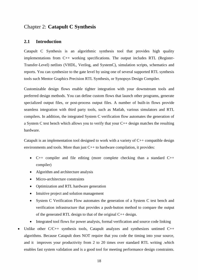
The process of high-level synthesis starts by analyzing the data dependencies between the
various steps in the algorithm shown in Figure 2-1. This analysis leads to a Data Flow Graph
(DFG).
Each node of the DFG represents an operation defined in the C++ code. The connection
between nodes represents data dependencies and indicates the order of operations.
2.3.2 Resource Allocation
Once the DFG has been assembled, each operation is mapped onto a hardware resource
which is then used during scheduling once the DFG has been assembled; each operation is
mapped onto a hardware resource which is then used during scheduling. The resource
corresponds to a physical implementation of the operator hardware. This implementation is
annotated with both timing and area information which is used during scheduling. Any given
operator may have multiple hardware resource implementations that each have different
Figure 2-1: Data flow graph description

22
area/delay/latency trade-offs. It is also typical that designers can explicitly control resource
allocation to insert pipeline registers or limit the number of available resources.
2.3.3 Scheduling
High-level synthesis adds "time" to the design during the process known as "scheduling".
Scheduling takes the operations described in the DFG and decides when (in which clock
cycle) they are performed. This has the effect of adding registers between operations based
on a target clock frequency. This is similar to what RTL designers would call pipelining, by
which they mean inserting registers to reduce combinational delays. This is shown in Figure
2-3.
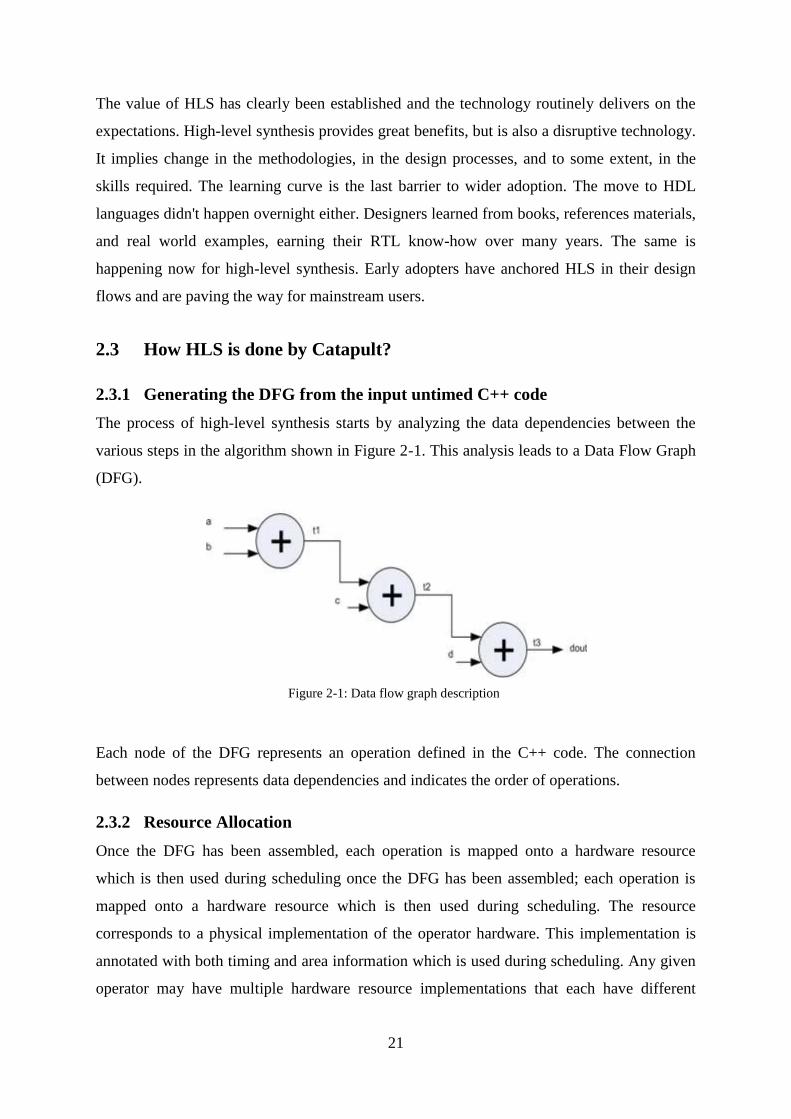
A data path state machine (DPFSM) is created to control the scheduled design. In HLS these
state are also referred to as control steps or c-steps (Figure 2-4).
Figure 2-2: Resource Allocation
Figure 2-3: Scheduling design
23
2.3.4 Loops
Loops are the primary mechanism for applying high level synthesis constraints as well as
moving data, or IO, into and out of an algorithm. The style in which loops are written can
have a significant impact on the quality of results of the generated hardware.
Loop Pipelining 2.3.4.1
Allows a new iteration of a loop to be started before the current iteration has finished, and it
allows also the execution of the loop iterations to be overlapped, increasing the design
performance by running them in parallel. The amount of overlap is controlled by the
"Initiation Interval (II)". This also determines the number of pipeline stages
Rolled Loop 2.3.4.2
If a loop is left rolled, then each iteration of the loop takes at least one clock cycle to execute
in hardware. This is because there is an implied ―wait until clock‖ for the loop body as shown
in Figure 2-5.
Figure 2-4: Datapath State Diagram

24
Each call to the ―accumulate‖ function requires four clock cycles to accumulate the four 32-
bit values. This is because the loop has been left rolled and there is an implied ―wait until
clock‖ at the end of the loop body.
Loop Unrolling 2.3.4.3
Loop unrolling is the primary mechanism to add parallelism into a design. This is done by
automatically scheduling multiple loop iterations in parallel, when possible. The amount of
parallelism is controlled by how many loop iterations are run in parallel. This is different than
loop pipelining, which allows loop iterations to be started every II clock cycles .loop
unrolling can theoretically execute all loop iterations within a single clock cycle as long as
there are no dependencies between successive iterations. And it does not necessarily
guarantee that the loop iterations are scheduled in the same c-step. Dependencies between
iterations can limit parallelism.
Figure 2-5: Schedule for accumulate using loops
25
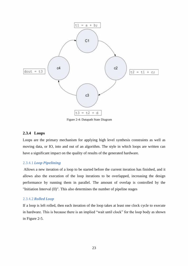
2.3.4.3.1 Partial Loop Unrolling
It has the equivalent effect of manually duplicating the loop body two times and running the
ACCUM loop for half as much iteration shown in Figure 2-6.
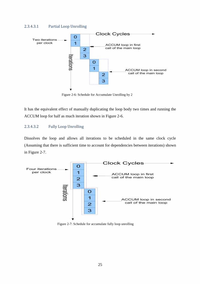
2.3.4.3.2 Fully Loop Unrolling
Dissolves the loop and allows all iterations to be scheduled in the same clock cycle
(Assuming that there is sufficient time to account for dependencies between iterations) shown
in Figure 2-7.
Figure 2-6: Schedule for Accumulate Unrolling by 2
Figure 2-7: Schedule for accumulate fully loop unrolling
26
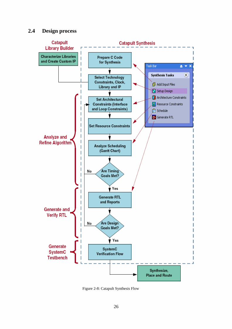
2.4 Design process
Figure 2-8: Catapult Synthesis Flow

27
2.4.1 Step 1: Writing and Testing the C Code
You can use drawings, MATLAB, C++ code or some other abstract design language to
model the design. The algorithm you use will have more effect on the final hardware than any
other step in this process, so an abstract representation is essential to a good design. Catapult
C Synthesis requires C++ code as an input, and accepts both untimed ANSI C++ and System
C The code allowed for synthesis is a subset of standard C++ including all the operators,
classes, templates and other structures in the language. Catapult doesn't support dynamic
memory allocation, so ―malloc,‖ ―free‖ and function recursion are not allowed. Catapult also
has some minor restrictions about how pointers are used, but any algorithm can be written
within these restrictions. Catapult provides an integrated text editor and includes more in-
depth C++ checking than standard C++ compilers, so the best approach is to use Catapult
while you are developing your algorithm.
The C++ code can be tested using any standard C++ simulation framework. Catapult also
provides the SC Verify flow, an internal verification flow that can simulate your C++ design
and also validate the cycle-accurate (or RTL) netlist output from Catapult against the original
C++ input using the user-supplied C++ testbench.
2.4.2 Step 2: Analyzing the Algorithm
Catapult provides a suite of algorithm and design analysis tools. The algorithm is analyzed
with respect to the target hardware and clock speed because these constraints play an
important role in determining how an algorithm is structured.
Setup Design 2.4.2.1
From the setting tab in constraint editor tab we can select the target technology, design
frequency and compatible library.
2.4.2.1.1 Technology
Synthesis Tool: Catapult displays Precision RTL as the synthesis tool if the FPGA flow is
available and Design Compiler if the ASIC flow is available. Changing this option changes
the list of available technologies.
Select Technology: Technologies are sorted by vendor and the FPGA flow in Catapult
includes built-in support for many of the technologies from Xilinx and Altera. ASIC
28
customers need to run Catapult Library Builder to generate a Catapult library for their ASIC
technology.
Select technology options: FPGA technologies need to have their part and speed grade
selected. Speed grade has a major impact on the technology‘s performance. For ASIC
technologies a wide range of options, such as operating conditions may be available here.
2.4.2.1.2 Compatible library
The basic components for a technology are automatically included, but any additional
components, such as RAMs need to be selected. Catapult automatically uses any RAM
components selected, so the selections made here can have a significant impact on the
generated design.
2.4.2.1.3 Design Frequency
Enter the target frequency in MHz.
2.4.2.1.4 Optimization
Carry-Save Adders: This optimization uses AND-OR logic to implement adder-trees and
constant multiplications using carry-save adder techniques. This leads to higher throughput,
lower latency designs. NOTE: The CSA optimization is only available in the Catapult SL
product.
The default value is -1 which defers the setting to the value that is defined in the technology
library being used. In the case of FPGA technologies that are shipped with Catapult, the
library setting is off. For the sample ASIC technology libraries that are shipped the library
value is on.
Constant Multipliers: This optimization implements constant multipliers using adder trees
and carry-save adder (CSA) optimizations leading to higher performance designs. The default
value is -1 which defers the setting to the value that is defined in the technology library being
used. In the case of FPGA technologies that are shipped with Catapult, the library setting is
off (0). For the sample ASIC technology libraries that are shipped the library value is on (1).
2.4.2.1.5 Array Size
This option specifies the default array size to be created for pointer variables on the
interface. When initially loading design source code, Catapult creates arrays for each pointer
variable on the design interface. ARRAY_SIZE specifies the initial size of each array.

29
Catapult then tries to reduce the size of the arrays by assessing how each pointer is used in
the design. On the Task Bar to access the Interface Control settings from the Constraint
Editor.
2.4.2.1.6 Setting Global Hardware Constraint
This is where you specify the clock frequency, reset and enable behavior. This is also where
you can enable process level handshake signals. Select an interface element in the Interface
Control section shown in Figure 2-9, and the editable constraints for that element appear.
You must expand the clock to access the reset and enable settings.
Architecture Constraints 2.4.2.2
On the task Bar to edit the I/O, loop and memory architectures in the Constraint Editor.
2.4.2.2.1 Setting I/O, Loop and Memory Architecture Constraints
Select a design element in the hierarchical view on the left and its editable constraints appear
on the right shown in Figure 2-10.
Catapult infers the I/O ports from the formal parameters of the top level the C/C++ function.
For each I/O parameter, Catapult creates a port resource to associate data variables with their
respective hardware components.
Figure 2-9: Catapult Interface Control Section

30
2.4.2.2.2 Set Loop Constraint
The left side of the Constraint Editor window is a graphical representation of the design that
provides information about the hardware inferred from the C++ including interfaces, data
structures, and loops, and all items are cross-referenced to the C++ code, so selecting an item
in the graphical view displays the editable options and constraints for that item on the right
side of the window. Catapult runs limited symbolic analysis of the design to determine the
number of iterations in each loop in your design. A number that is larger or smaller than you
expected can point to an error or inefficiency in your algorithm. If Catapult can't determine
the number of iterations, you might want to modify the algorithm or add an iteration
constraint as shown in Figure 2-11.
Figure 2-11: Catapult loop iteration constraint
Figure 2-10: Input output settings
31
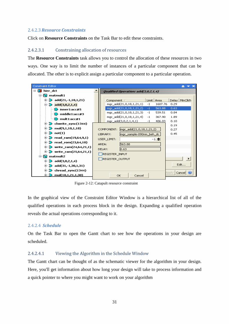
Resource Constraints 2.4.2.3
Click on Resource Constraints on the Task Bar to edit these constraints.
2.4.2.3.1 Constraining allocation of resources
The Resource Constraints task allows you to control the allocation of these resources in two
ways. One way is to limit the number of instances of a particular component that can be
allocated. The other is to explicit assign a particular component to a particular operation.
In the graphical view of the Constraint Editor Window is a hierarchical list of all of the
qualified operations in each process block in the design. Expanding a qualified operation
reveals the actual operations corresponding to it.
Schedule 2.4.2.4
On the Task Bar to open the Gantt chart to see how the operations in your design are
scheduled.
2.4.2.4.1 Viewing the Algorithm in the Schedule Window
The Gantt chart can be thought of as the schematic viewer for the algorithm in your design.
Here, you'll get information about how long your design will take to process information and
a quick pointer to where you might want to work on your algorithm
Figure 2-12: Catapult resource constraint

32
In addition to the loop profile, you get a full view of the functional units in your design. This
is a view of the data path without the multiplexers used for sharing. You can look at these
operations to make sure you have the bit widths you expect. Catapult C Synthesis will
optimize the bit widths of all the variables in your design based on a symbolic analysis of the
design. Some styles of C++ code prevent bitwidth optimization. In this case, you can change
your loop constraints or your source code to quickly see the effect of these changes
Generating RTL 2.4.2.5
On the Task Bar Catapult generates one or more RTL netlist (VHDL, Verilog or SystemC),
report files, and control files for running downstream tools .some of these reports are more
hardware-centric, while others provide a quick summary of your algorithm‘s characteristics
.The reports also cross-probe back to the C source giving you one more analysis tools to help
you improve your algorithm.
2.4.3 Step 3: Creating the Hardware Design
It's time to set some hardware constraints. This entire process only takes a few minutes and
can be changed any number of times for the same design. Catapult C Synthesis insures that
all of your work is saved during a session and you can save your work if you want to come
back later.
2.4.4 Step 4: Performing Timed Simulation
Catapult provides both a Behavioral and RTL level output. Both these outputs simulate
exactly the same at their interfaces. The Behavioral output is for simulation only, and it
Figure 2-13: Catapult Schedule Window
33
simulates at about 30 X faster than RTL. Since the output of Catapult is standard VHDL,
Verilog or SystemC, your normal testing flow can be used to verify that this output is correct
In addition, Catapult provides an integrated SystemC verification flow that automates the
process of validating the cycle-accurate (or RTL) netlist output from Catapult against the
original C/C++ input.
2.4.5 Step 5: Synthesizing the RTL design
Catapult provides total integration with other Mentor Graphics Synthesis products. All of the
required constraints are written to a file that can be read into the Precision RTL Synthesis and
Precision Physical Synthesis products. The Precision Synthesis products can then be used as
though you were synthesizing any other RTL design.
2.5 Design Example “FIR”
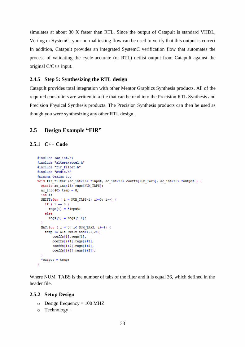
2.5.1 C++ Code
Where NUM_TABS is the number of tabs of the filter and it is equal 36, which defined in the
header file.
2.5.2 Setup Design
o Design frequency = 100 MHZ
o Technology :

34
Synthesis tool : precision
Target FPGA: Stratix II EP2S15F484C3
o Compatible library: Altera Accelerated Library & Base FPGA Library
2.5.3 Architecture Constraints
Design
goal
Loop unrolling Loop
pipelining
Design
#1
Area None None
Design
#2
Area All loops are partial unrolled by 2 None
Design
#3
Area None Main loop
(II=1)
Design
#4
Latency None None
Design
#5
Latency All loops are partial unrolled by 2 None
Design
#6
Latency Main loop is partially unrolled by 2 & (shift &
mac) loops partially unrolled by 12
None
Design
#7
Latency Main loop is partially by 18 & (shift &
mac)loops partially unrolled by 12
None
Design
#8
Latency None Main loop
(II=1)
Design
#9
Latency (shift & mac) loops are partially unrolled by 12 Main loop
(II=1)
Design
#10
Area (shift & mac) loops partial unrolled by 12 Main loop
(II=1)
Table 2-2: Design Constraint Table
35
2.5.4 Results
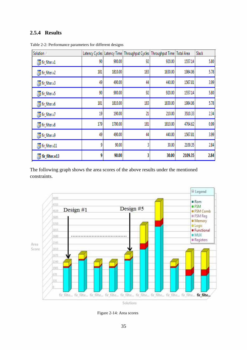
The following graph shows the area scores of the above results under the mentioned
constraints.
Table 2-2: Performance parameters for different designs
Figure 2-14: Area scores

36
Figure 2-15: Timing scores

37
Object Tracking Using Mean-Shift Algorithm Chapter 3:
3.1 Introduction
Object tracking is an important task within the field of computer vision. The proliferation of
high-powered computers, the availability of high quality and inexpensive video cameras, and
the increasing need for automated video analysis has generated a great deal of interest in
object tracking algorithms. There are three key steps in video analysis: detection of
interesting moving objects, tracking of such objects from frame to frame, and analysis of
object tracks to recognize their behavior. Therefore, the use of object tracking is pertinent in
the tasks of:
Motion-based recognition, which is, human identification based on automatic object
detection
Automated surveillance, which is, monitoring a scene to detect suspicious activities or
unlikely events.
Traffic monitoring, which is, real-time gathering of traffic statistics to direct traffic
flow.
Vehicle navigation, which is, video-based path planning and obstacle avoidance
capabilities.
In its simplest form, tracking can be defined as the problem of estimating the trajectory of an
object in the image plane as it moves around a scene. In other words, a tracker assigns
consistent labels to the tracked objects in different frames of a video. Additionally, depending
on the tracking domain, a tracker can also provide object-centric information, such as
orientation, area, or shape of an object. Tracking objects can be complex due to:
Loss of information caused by projection of the 3D world on a 2D image.
Noise in images.
Complex object motion.
Non-rigid or articulated nature of objects.
Partial and full object occlusions.
Complex object shapes.
Scene illumination changes.
Real-time processing requirements.
38
One can simplify tracking by imposing constraints on the motion and/or appearance of
objects. For example, almost all tracking algorithms assume that the object motion is smooth
with no abrupt changes. One can further constrain the object motion to be of constant velocity
or constant acceleration based on a priori information. Prior knowledge about the number and
the size of objects, or the object appearance and shape, can also be used to simplify the
problem.
In this chapter, we will follow a bottom-up approach in describing the issues that need to be
addressed when one sets out to build an object tracker. The first issue is defining a suitable
representation of the object, for example, points, primitive geometric shapes and object
contours, and appearance representations. The next issue is the selection of image features
used as an input for the tracker, such as color, motion, edges, etc., which are commonly used
in object tracking. Almost all tracking algorithms require detection of the objects either in the
first frame or in every frame. Then, we will introduce the Mean-Shift tracking algorithm and
its hardware implementation issues.
3.2 Object Representation
In a tracking scenario, an object can be defined as anything that is of interest for further
analysis. For instance, boats on the sea, fish inside an aquarium, vehicles on a road, planes in
the air, people walking on a road, or bubbles in the water are a set of objects that may be
important to track in a specific domain. Objects can be represented by their shapes and
appearances. In this section, we will first describe the object shape representations commonly
employed for tracking and then address the joint shape and appearance representations.
3.2.1 Object Shape Representation
Points 3.2.1.1
The object is represented by a point, that is, the centroid (Figure 3-1(a)) or by a set of points
(Figure 1(b)). In general, the point representation is suitable for tracking objects that occupy
small regions in an image.
Primitive geometric shapes 3.2.1.2
Object shape is represented by a rectangle, ellipse (Figure 3-1(c), (d)). Object motion for such
representations is usually modeled by translation, affine, or projective transformation.
Though primitive geometric shapes are more suitable for representing simple rigid objects.
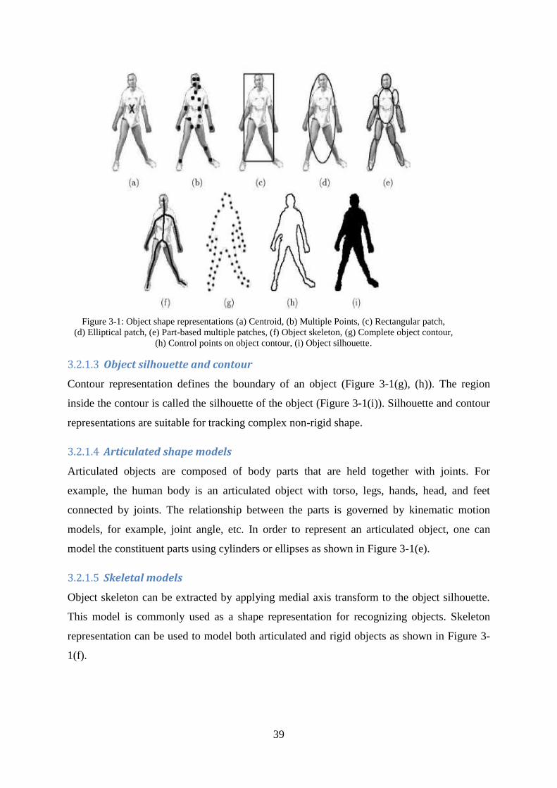
39
Object silhouette and contour 3.2.1.3
Contour representation defines the boundary of an object (Figure 3-1(g), (h)). The region
inside the contour is called the silhouette of the object (Figure 3-1(i)). Silhouette and contour
representations are suitable for tracking complex non-rigid shape.
Articulated shape models 3.2.1.4
Articulated objects are composed of body parts that are held together with joints. For
example, the human body is an articulated object with torso, legs, hands, head, and feet
connected by joints. The relationship between the parts is governed by kinematic motion
models, for example, joint angle, etc. In order to represent an articulated object, one can
model the constituent parts using cylinders or ellipses as shown in Figure 3-1(e).
Skeletal models 3.2.1.5
Object skeleton can be extracted by applying medial axis transform to the object silhouette.
This model is commonly used as a shape representation for recognizing objects. Skeleton
representation can be used to model both articulated and rigid objects as shown in Figure 3-
1(f).
Figure 3-1: Object shape representations (a) Centroid, (b) Multiple Points, (c) Rectangular patch,
(d) Elliptical patch, (e) Part-based multiple patches, (f) Object skeleton, (g) Complete object contour,
(h) Control points on object contour, (i) Object silhouette.
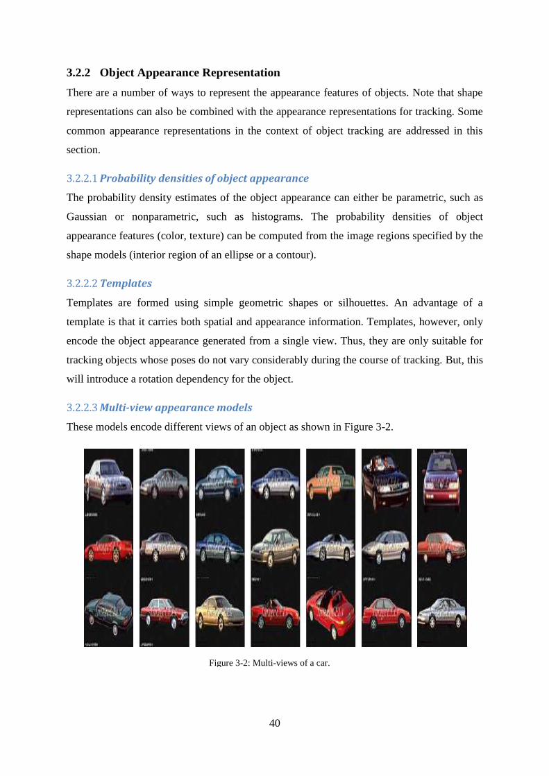
40
3.2.2 Object Appearance Representation
There are a number of ways to represent the appearance features of objects. Note that shape
representations can also be combined with the appearance representations for tracking. Some
common appearance representations in the context of object tracking are addressed in this
section.
Probability densities of object appearance 3.2.2.1
The probability density estimates of the object appearance can either be parametric, such as
Gaussian or nonparametric, such as histograms. The probability densities of object
appearance features (color, texture) can be computed from the image regions specified by the
shape models (interior region of an ellipse or a contour).
Templates 3.2.2.2
Templates are formed using simple geometric shapes or silhouettes. An advantage of a
template is that it carries both spatial and appearance information. Templates, however, only
encode the object appearance generated from a single view. Thus, they are only suitable for
tracking objects whose poses do not vary considerably during the course of tracking. But, this
will introduce a rotation dependency for the object.
Multi-view appearance models 3.2.2.3
These models encode different views of an object as shown in Figure 3-2.
Figure 3-2: Multi-views of a car.
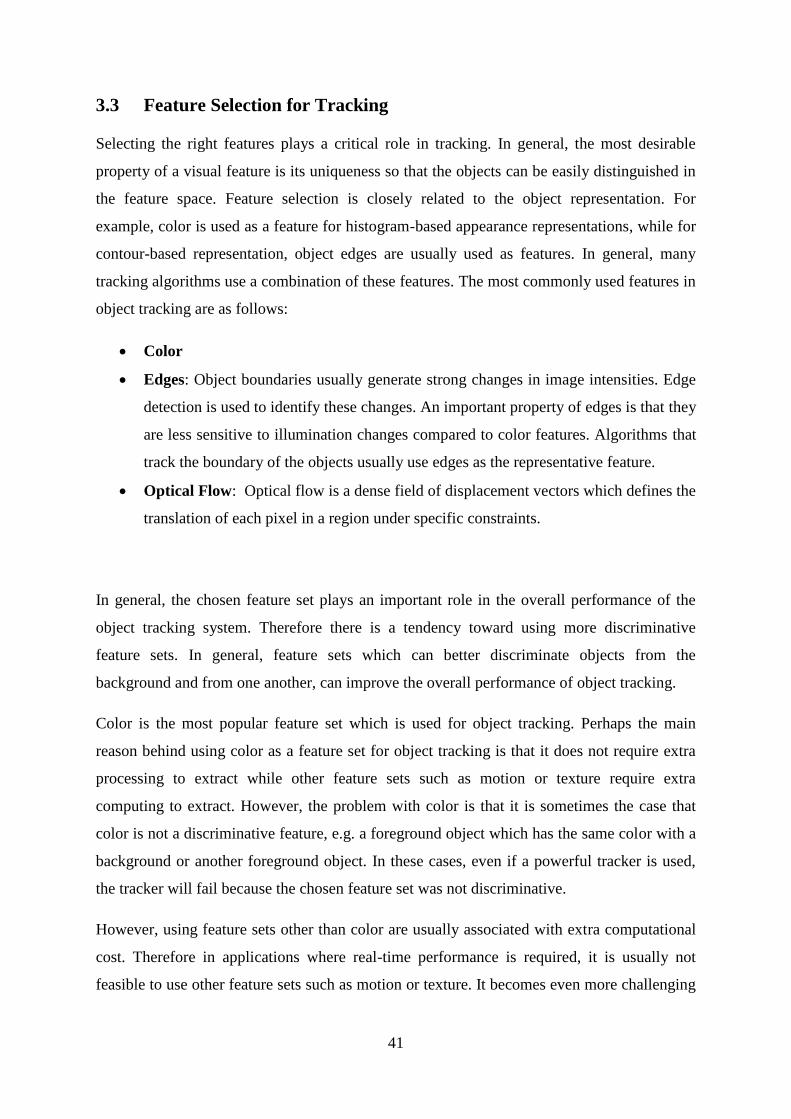
41
3.3 Feature Selection for Tracking
Selecting the right features plays a critical role in tracking. In general, the most desirable
property of a visual feature is its uniqueness so that the objects can be easily distinguished in
the feature space. Feature selection is closely related to the object representation. For
example, color is used as a feature for histogram-based appearance representations, while for
contour-based representation, object edges are usually used as features. In general, many
tracking algorithms use a combination of these features. The most commonly used features in
object tracking are as follows:
Color
Edges: Object boundaries usually generate strong changes in image intensities. Edge
detection is used to identify these changes. An important property of edges is that they
are less sensitive to illumination changes compared to color features. Algorithms that
track the boundary of the objects usually use edges as the representative feature.
Optical Flow: Optical flow is a dense field of displacement vectors which defines the
translation of each pixel in a region under specific constraints.
In general, the chosen feature set plays an important role in the overall performance of the
object tracking system. Therefore there is a tendency toward using more discriminative
feature sets. In general, feature sets which can better discriminate objects from the
background and from one another, can improve the overall performance of object tracking.
Color is the most popular feature set which is used for object tracking. Perhaps the main
reason behind using color as a feature set for object tracking is that it does not require extra
processing to extract while other feature sets such as motion or texture require extra
computing to extract. However, the problem with color is that it is sometimes the case that
color is not a discriminative feature, e.g. a foreground object which has the same color with a
background or another foreground object. In these cases, even if a powerful tracker is used,
the tracker will fail because the chosen feature set was not discriminative.
However, using feature sets other than color are usually associated with extra computational
cost. Therefore in applications where real-time performance is required, it is usually not
feasible to use other feature sets such as motion or texture. It becomes even more challenging

42
in the case of smart cameras and embedded vision systems with limited computational and
memory resources.
3.4 Mean-Shift Algorithm for Object Tracking
Mean-shift is a popular tracking algorithm that is computationally less intensive. The mean-
shift tracking algorithm is an iterative algorithm which uses the probability distribution of a
target region and a candidate region to find the best candidate model in the next frame based
on the target model in the current frame. A similarity function is used in each iteration, in
which it should be maximized to find the target candidate in the next frame.
Main properties of the mean-shift tracking algorithm:
Rotation independent
Zooming independent
Mean-shift tracking algorithm is composed of four main stages which are explained as
follows.
3.4.1 Target Model
The target is represented by the square region of equal width and height h. The target model
is computed as follows:
∑ (‖ ‖ )
( ) (3.1)
Where xi, i =1,2…,n are the normalized pixel locations, n is number of pixels in reference
image, u = 1 ... M, M is number of bins, and k(x) is the kernel function and is the kronecker
delta function. The constant C is derived using the following equation:
∑ (‖ ‖ )
(3.2)
Also, the used kernel function is the Epanechnikov Kernel:
( ) { ( (‖ ‖ ) ‖ ‖
(3.3)
Epanechnikov Kernel is plotted versus the scaled squared distance in Figure 3-3.

43
3.4.2 Target Candidate Model
The target candidate model is defined using the following equation :
( ) ∑ (‖
‖
) ( ) (3.4)
Where xi, i =1,2…, nh are the normalized pixel locations with nh pixels centered at y in the
current frame, Ch is the normalization constant with a following equation
∑ (‖ ‖ )
(3.5)
3.4.3 Similarity Function
A similarity measure has to be used to define a distance between target and candidate models.
Bhattacharyya Coefficient is used as similarity measure between the target and candidate
model. The sample estimate between two discrete distributions of p and q can be computed
using the following equation:
( ( )) ∑ √ ( ) (3.6)
Where q and p(y) are the target model and the candidate model respectively, and they are
calculated according to Eq. (3.1) and (3.4) respectively, M is the number of bins in these
histograms.
Figure 3-3: a) 2-D Epanechnikov Kernel b) 3-D Epanechnikov Kernel
(a) (b)

44
3.4.4 Target Localization
To find the location corresponding to the target in the current frame, the distance should be
minimized. Minimizing this distance is equivalent to maximizing Bhattacharyya coefficient.
In this procedure, the kernel is recursively moved from the initial location of yo to the new
location y1 using Eq. (3.7). This process is done iteratively until the convergence or
predefined maximum iteration number reached. In our current implementation, the maximum
number of iteration is fixed to twenty.
∑
∑
(3.7)
Where wi is calculated as follows:
∑ √
( ) ( ) (3.8)
So, the complete flowchart of the mean-shift is shown in Figure 4-4.
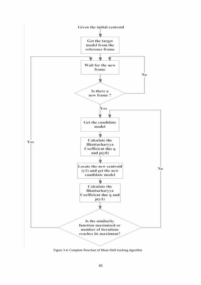
45
Figure 3-4: Complete flowchart of Mean-Shift tracking algorithm

46
3.5 Modifications on the Mean-Shift Algorithm
3.5.1 Epanechnikov Kernel Calculation
By observing Equ. (3.4) and Equ. (3.4), the only difference is between them is the number
of pixels but according to the assumption of constant scale of the object during tracking and
alse the maximum target size is 32x32, then the number of pixels is 1024 in both cases. Also,
the normalized pixels locations are the same in both cases, because they are referred to the
candidate center as shown in Figure 3-5.
Suppose that the target object size is 3x3, then there are 9 pixels in the target model, if the
index of each pixel is referred to the centre object, these normalized locations would be the
same.
In the reference frame, the center is (5,5), and the index of the first pixel of the target model
is (4,4), so if we refer this index to the center, it will be (-1,-1). In the next frame, the center is
(6,6), and the index of the first pixel of the candidate model is (5,5), so if we refer this index
to the center, it will be (-1,-1). So, the same case will happen for the squared distance
measured from the center.
So, the Epanechnikov Kernel values will be the same in each frame. Also the normalization
constant C or Ch value will be determined.
0 0 0 0 0 0 0 0 0
0 0 0 0 0 0 0 0 0
0 0 0 0 0 0 0 0 0
0 0 0 255 255 255 0 0 0
0 0 0 255 255 255 0 0 0
0 0 0 255 255 255 0 0 0
0 0 0 0 0 0 0 0 0
0 0 0 0 0 0 0 0 0
0 0 0 0 0 0 0 0 0
(a) Reference frame
0 0 0 0 0 0 0 0 0
0 0 0 0 0 0 0 0 0
0 0 0 0 0 0 0 0 0
0 0 0 0 0 0 0 0 0
0 0 0 0 255 255 255 0 0
0 0 0 0 255 255 255 0 0
0 0 0 0 255 255 255 0 0
0 0 0 0 0 0 0 0 0
0 0 0 0 0 0 0 0 0
(b) Next frame
Figure 3-5: Object is two frames

47
So, these values are stored in a ROM using the embedded array block of the FPGA to save
the time required for their calculation as they could be pre-determined from the boundary
conditions of the problem.
3.5.2 Weights Calculation
The most computationally intensive task in this algorithm is computation of weights in Equ.
(4.8) as it involves square root and division.
The number of iterations according to Equ. (3.7) is equal to the number of pixels in the ROI
which is 1024. But, in fact, the number of different calculations is restricted only the number
of bins of the target or candidate model which is 256. So, the number of square root and
division operations is restricted to 256 which decrease the difficulty of the weights
calculation.
3.6 Developing the Algorithm for Colored Object Tracking
3.6.1 HSV representation
Most operating systems, image processing programs and texts treat images as collections of
pixels comprised of red, green and blue values. This is very convenient for display purposes,
since computer monitors output color by combining different amounts of red, green and blue.
However, most users don‘t think of color in these terms. They tend to think about color the
same way they perceive it - in terms of hue (the English name we give colors, like ―reddish‖
or ―greenish‖), purity (pastels are ―washed out‖, saturated colors are ―vibrant‖), and
brightness (a stop sign is ―bright‖ red, a glass of wine is ―dark‖ red). So scientists came up
with what they call perceptual color spaces. A perceptual color space represents color in
terms that non-technical people understand. There are many perceptual color spaces,
including the PANTONE® Color System, the Munsell Color System, HSV (Hue, Saturation,
Value) space, HLS (Hue, Lightness , Saturation) space, and countless others.
The HSV color space is a cone as mentioned by Figure 3-6.Viewed from the circular side of
the cone, the hues are represented by the angle of each color in the cone relative to the 0°
line, which is traditionally assigned to be red. The saturation is represented as the distance
from the center of the circle. Highly saturated colors are on the outer edge of the cone,
whereas gray tones (which have no saturation) are at the very center. The brightness is

48
determined by the colors vertical position in the cone. At the pointy end of the cone, there is
no brightness, so all colors are black. At the fat end of the cone are the brightest colors.
3.6.2 RGB to HSV transformation:
The RGB color space is conceptually a cube with one axis representing red, one representing
green, and one representing blue, as shown in Figure 3-7.
As you can see, where the axes meet at (0,0,0), we have black, and at (255,255,255) (or
(1.0,1.0,1.0) if you prefer), we have white. How do we tell if a color in an image is close to a
color we picked? We could take the Euclidian distance between the two colors and see if it‘s
less than a ―similarity‖ parameter. That sounds reasonable, but let‘s look at how this works
from a perceptual standpoint. Let‘s say you allow the user to set a ―similarity‖ threshold for
Figure 3-6: The HSV Cone
Figure 3-7: RGB cube representation

49
matching all colors that are similar to a chosen color. In RGB space, all points that are less
than or equal to the ―similarity‖ distance from the chosen color form a sphere inside the RGB
cube. The user probably thinks of matching a color by choosing ―all the bluish tones‖, or
some similar perceptual way. But the sphere we get in the RGB cube doesn‘t include many of
the values that would meet this criterion, and it does include many that probably wouldn‘t.
You can shrink the sphere to remove those which don‘t match, but there is no obvious
transform you can perform to get more of those colors which don‘t match, but that you want
to include.
Another way to match colors in RGB space would be to pick a range of red, green, and blue
in which colors must fall. So now you‘ve cut out a smaller cube from the RGB cube. If you
want to, say, match purplish colors, you run into a similar problem as with using a Euclidian
distance. Since the purplish colors run along the diagonal between the red and blue axes, you
either end up including a bunch of points you don‘t want, not including points you do want,
or doing a whole bunch of math for what should be an easy problem.
Now let‘s see how you would make such a match in HSV space. The user picks a color, and
sets a similarity control. You convert the color to HSV space, if it isn‘t already in HSV space.
Now you can see if other colors match the chosen one based on their hue angle. If the user
wants only aqua colors, they will likely choose a color with a hue angle of 180°. Colors that
match have hues of roughly 165° to 195°. Using those parameters you cut a pie slice out of
the HSV cone. The user probably doesn‘t want very dark cyans, since colors that are close to
black often appear to be black. And she probably doesn‘t want colors that are too close to
gray or white, either. So we can limit the colors that match to not only be within a given hue
range, but also a given saturation and value range. Brief experimentation with the HSV color
picker suggests that a saturation of 25% or greater, and a value of 50% or greater gets us a
nice range of colors that most users would probably qualify as ―close to aqua‖. So allowing
the user to choose a range for the hue, a range for the saturation, and a range for the value
gets us reasonable results. This is easier for the user, and as you‘ll see below, fairly easy for
the programmer, too.
As you can see, working in HSV space offers several opportunities for improving the ease of
use of color input from users, improved color matching within your application, and lots of
really cool filters for a variety of applications. However, there are some things you need to
watch out for when using HSV space. The gray tones, from black to white, have undefined
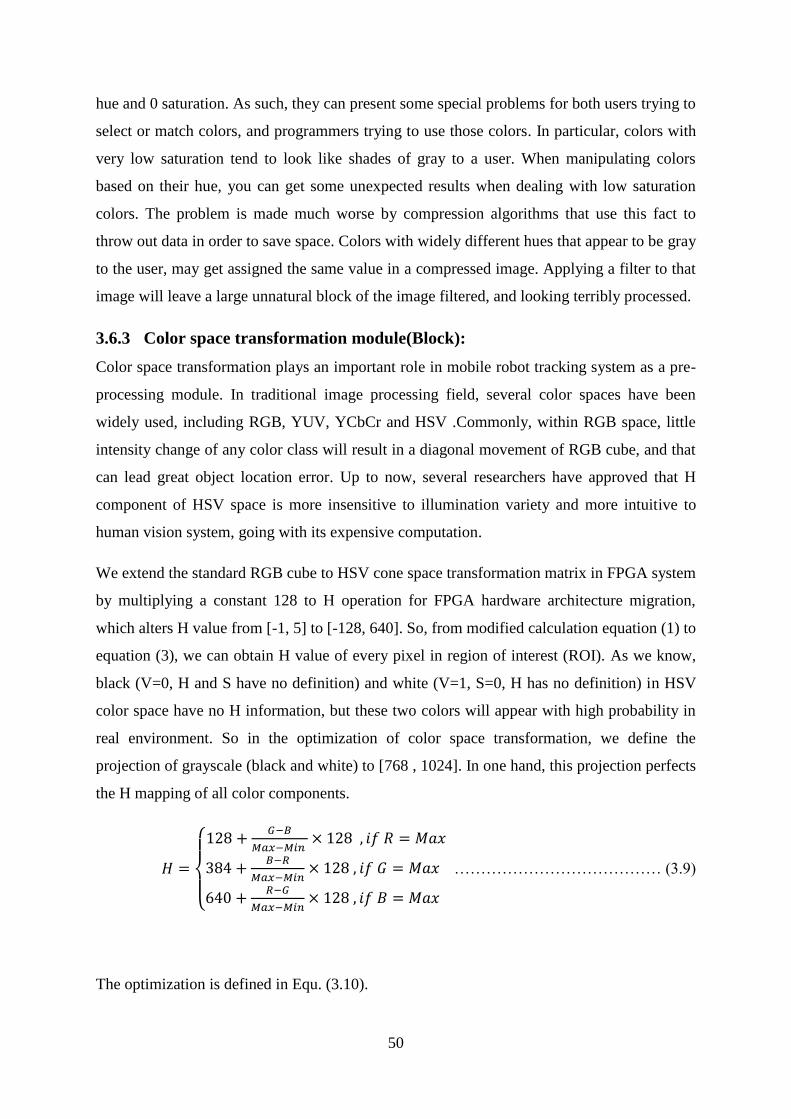
50
hue and 0 saturation. As such, they can present some special problems for both users trying to
select or match colors, and programmers trying to use those colors. In particular, colors with
very low saturation tend to look like shades of gray to a user. When manipulating colors
based on their hue, you can get some unexpected results when dealing with low saturation
colors. The problem is made much worse by compression algorithms that use this fact to
throw out data in order to save space. Colors with widely different hues that appear to be gray
to the user, may get assigned the same value in a compressed image. Applying a filter to that
image will leave a large unnatural block of the image filtered, and looking terribly processed.
3.6.3 Color space transformation module(Block):
Color space transformation plays an important role in mobile robot tracking system as a pre-
processing module. In traditional image processing field, several color spaces have been
widely used, including RGB, YUV, YCbCr and HSV .Commonly, within RGB space, little
intensity change of any color class will result in a diagonal movement of RGB cube, and that
can lead great object location error. Up to now, several researchers have approved that H
component of HSV space is more insensitive to illumination variety and more intuitive to
human vision system, going with its expensive computation.
We extend the standard RGB cube to HSV cone space transformation matrix in FPGA system
by multiplying a constant 128 to H operation for FPGA hardware architecture migration,
which alters H value from [-1, 5] to [-128, 640]. So, from modified calculation equation (1) to
equation (3), we can obtain H value of every pixel in region of interest (ROI). As we know,
black (V=0, H and S have no definition) and white (V=1, S=0, H has no definition) in HSV
color space have no H information, but these two colors will appear with high probability in
real environment. So in the optimization of color space transformation, we define the
projection of grayscale (black and white) to [768 , 1024]. In one hand, this projection perfects
the H mapping of all color components.
{
………………………………… (3.9)
The optimization is defined in Equ. (3.10).

51
{
…………………...……(3.10)
Now, our histogram is the H‘s values and we apply the same algorithm of the Gray-scale
Mean-Shift. We choose the length of H to be 1024 element for more color details to increase
the efficiency of tracking by extracting more details from the object histogram to be more
significant with comparing to the background details..

52
Design Implementation Chapter 4:
An optimized hardware implementation of the mean shift tracking algorithm is required to
achieve the tracking in real-time at full frame rate. The maximum target size is limited to
32x32. The number of bins is 256. The number of mean shift iterations is limited to 16.
Practically the average number of iterations is much smaller, nearly 8. The scale of the target
model is considered constant throughout tracking. In this section, we will address the
optimizations and modifications in the algorithm in order to achieve the tracking in real-time
at full frame rate at reasonable number of logic elements. The target FPGA is
EP3C25F324C6.
Figure 4-1: Design Procedure

53
4.1 Developing Floating Point MATLAB Model
We had first to develop the mean-shift tracking algorithm and verify if it performs as required
or not. We used MATLAB as an easy and powerful high level language for modeling
purposes. MATLAB provides a rich set of built-in functions and libraries for video and image
processing and for digital signal processing in general.
We used the data import and export functions for reading video files and creating new video
files after executing the developed algorithm. We used also the Image Processing Toolbox for
developing the algorithm and checking its validity.
The main processes as histogram calculation, Bhattacharyya coefficients, kernel
function…etc, were implemented as separate functions to ease the debugging of errors.
In order to verify the algorithm we generated a set of frames with the object moving along the
diagonal direction with a constant 5 pixels displacement per frame. We applied these frames
to the developed algorithm and used the output centroids as a performance metric for the
correctness of the algorithm.
4.2 Developing the Floating Point C Model
As a step to be near to the HW implementation and near to the C code used for the HLS tool
for RTL generation, we made another floating point model with C and also verified the
obtained results from it.
The compilation and execution of the C code was much faster than the execution of the
MATLAB model as the last is a scripting language in which the code is translated into
another form before execution. This was the main advantage of using the C programming
language for modeling, the fast execution which enables the fast modification of the
algorithm and checking errors.
In order to read and write video and image files with C, we used the OpenCV library. With its
focus on real-time vision, OpenCV helps students and professionals efficiently implement
projects and jump-start research by providing them with a computer vision and machine
learning infrastructure that was previously available only in a few mature research labs.

54
4.3 Developing the Fixed Point C Model
A fixed-point model is an essential step in order to build a robust design that achieves your
pre-specified requirements with a minimum HW, as using floating point arithmetic to
implement the algorithm requires a very high computational cost.
As example, the floating point multiplication unit is much larger than its fixed point
counterpart, and dissipates more power. This is also the case for addition and division.
The fixed point model defines the error margin that design could operate within it. In our
design, the error in the output center of the target in a given frame has to be two-pixel
maximum, so the bit-widths of the design variables are chosen according to their dynamic
range and to satisfy this accuracy requirement by using a MATLAB or C++ model.
We choose each node in the design according to the estimated dynamic range of this node,
and by comparing this node to the corresponding node in the floating point model (for the
same set of inputs), and change its bit-width until the obtained results are satisfactory.
Some nodes have to be with a relatively large bit-width to accommodate the design
specifications, like the numerator of Equ. (3.7) which occupies 26 bits.
The last step in the code development was to write a fixed-point C code using the bit-accurate
data types provided by Mentor Graphics. These data types make the developer able to
implement fixed point nodes with all the mathematical operations done on them like:
multiplication, addition, division, square root, rounding and saturation.
We used this code also with the MS Visual C 2008 to check the algorithm on the SW level,
and then we used it with MG Catapult C synthesis tool for HLS.
4.4 HLS Using Catapult C Synthesis Tool
The fixed point C code is then given to the Catapult C synthesis tool to perform HLS and
generating the RTL code. First, we choose a required operating frequency and the target
technology (FPGA or ASIC) to give an indication to the tool for resource allocation and
scheduling.
55
Then, the architectural constraints are set for each loop in the code for each loop in the code.
We choose the preferences of (loop rolling, loop pipelining and loop merging) to optimize the
design for a certain requirement (area, speed, latency..Etc.).
Nest, we set constraints on the used resources for each operation in the code, the tool chooses
a certain resource according to the requirements set in the beginning. choose the resource
allocated.
After the scheduling is done, the Catapult generates a Gantt chart for the generated RTL to
show the C-steps of the code and the operations scheduled in each C-step.
The outputs of this step are separate .vhd files for the controller and the datapath, and also a
concat_rtl.vhd that includes all the used components in the design and the interconnections
between them.
4.5 Functional Simulation Using ModelSim
We built a VHDL testbench to verify whether the generated RTL code satisfy the proper
functionality or not. We used the generated (concat_rtl.vhd) file with this testbench in
ModelSim.
We faced a problem in ModelSim that each frame consists of 307200 pixel, with each pixel
in 8-bits, we tried to read all of them from a file and assign them to an array to each frame or
to include the frames directly in the VHDL code, but the ModelSim refused to deal with such
very large arrays.
The solution was to use the MATLAB as a scripting language to generate a VHDL code that
uses 75 arrays for each frame and use them directly in the VHDL code. This way worked for
us and the results were the same as the results from the behavioral description.
4.6 Logic Synthesis Using Precision RTL
The Catapult C synthesis tool generates makefiles and TCL files to order the Precision RTL
to perform the logic synthesis of the generated files. Also the concat_rtl.vhd file generated by
Catapult C can be used directly with the Precision RTL.
The output of this step is a gate netlist written in: VHDL, Verilog, or EDIF as we choose.
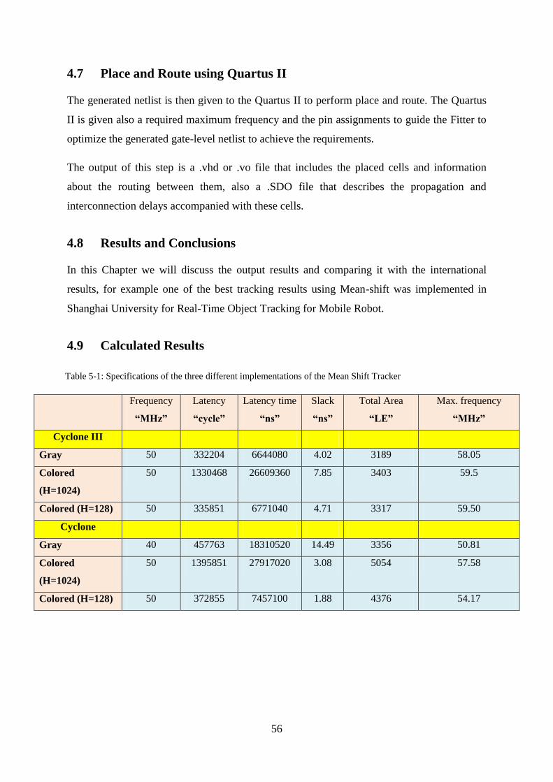
56
4.7 Place and Route using Quartus II
The generated netlist is then given to the Quartus II to perform place and route. The Quartus
II is given also a required maximum frequency and the pin assignments to guide the Fitter to
optimize the generated gate-level netlist to achieve the requirements.
The output of this step is a .vhd or .vo file that includes the placed cells and information
about the routing between them, also a .SDO file that describes the propagation and
interconnection delays accompanied with these cells.
4.8 Results and Conclusions
In this Chapter we will discuss the output results and comparing it with the international
results, for example one of the best tracking results using Mean-shift was implemented in
Shanghai University for Real-Time Object Tracking for Mobile Robot.
4.9 Calculated Results
Frequency
“MHz”
Latency
“cycle”
Latency time
“ns”
Slack
“ns”
Total Area
“LE”
Max. frequency
“MHz”
Cyclone III
Gray 50 332204 6644080 4.02 3189 58.05
Colored
(H=1024)
50 1330468 26609360 7.85 3403 59.5
Colored (H=128) 50 335851 6771040 4.71 3317 59.50
Cyclone
Gray 40 457763 18310520 14.49 3356 50.81
Colored
(H=1024)
50 1395851 27917020 3.08 5054 57.58
Colored (H=128) 50 372855 7457100 1.88 4376 54.17
Table 5-1: Specifications of the three different implementations of the Mean Shift Tracker

57
4.10 A Comparison with a similar tracker done by a team from Shanghai
University (Using classic RTL flows)
Frequency
“MHz”
Latency
“cycle”
Latency time
“ns”
Slack
“ns”
Total Area
“LE”
Max. frequency
“MHz”
Colored (HLS)
(H=128)
50 372855 7457100 1.88 4376 54.17
Ref. Colored (conv.
RTL flows) (H=128)
50 - - - 4039 -
Table 5-2: Comparison Results with a Cyclone FPGA

58
Testing &Verification Chapter 5:
5.1 Introduction
Verification is a process used to demonstrate the functional correctness of a design.
Testbench usually refers to the code used to create a pre-determined input sequence to a
design, and then optionally observe the response. It is commonly implemented using VHDL
or Verilog, but may also include external data files or C routines. Testbench provides inputs
to the design and monitors any outputs.
Verification is currently the target of new tools and methodologies. These tools and
methodologies attempt to reduce the overall verification time by enabling parallelism of
effort, higher levels of abstraction and automation. To parallelize the verification effort, it is
necessary to be able to write - and debug – Test benches in parallel with each others as well
as in parallel with the implementation of the design. Automation lets you do something else
while a machine completes a task autonomously, faster, and with predictable results.
Automation requires standard processes with well-defined inputs and outputs.
5.1.1 Formal Verification
Formal Verification flow falls under two broad categories equivalence checking and model
checking.
Equivalence Checking 5.1.1.1
It is a formal verification process mathematically proves that the origin and output are
logically equivalent and that the transformation preserved its functionality, equivalence
checking compares two netlists to ensure that some netlist post-processing did not change the
functionality of the circuit. Equivalence checking is a true alternative path to the logic
synthesis transformation being verified. It is only interested in comparing Boolean and
sequential logic functions, not mapping these functions to a specific technology while
meeting stringent design constraints.
Model Checking 5.1.1.2
In Model Checking, assertions or characteristics of a design are formally proven or
disproved. For example, all state machines in a design could be checked for unreachable or
isolated states. A more powerful model checker may be able to determine if deadlock
conditions can occur.
59
The main purpose of functional verification is to ensure that design implements intended
functionality. Without functional verification, one must trust that the transformation of a
specification document into RTL code was performed correctly.
The increasing popularity of code coverage and model checking tools has created a niche for
a new breed of verification tools: testbench generators. Using the code coverage metrics or
the results of some proof, and the source code under analysis, testbench generators generate
testbenches to either increase code coverage or to exercise the design to violate a property.
Testbenches generated from model checking results are useful only to illustrate how a
property can be violated and what input sequence leads to the improper behavior. It may be a
useful vehicle for identifying pathological conditions that were not taken into account in the
specification or to provide a debugging environment for fixing the problem.
5.1.2 Functional Verification Approaches
It‘s done using three complementary but different approaches: black-box, white-box, and
grey box. With a black-box approach, the functional verification must be performed without
any knowledge of the actual implementation of a design. All verification must be
accomplished through the available interfaces, without direct access to the internal state of
the design, without knowledge of its structure and implementation. This method suffers from
an obvious lack of visibility and controllability. The advantage of black-box verification is
that it does not depend on any specific implementation. Whether the design is implemented in
a single ASIC, multiple FPGAs, a circuit board. A white-box approach has full visibility and
controllability of the internal structure and implementation of the design being verified. This
method has the advantage of being able to quickly set up an interesting combination of states
and inputs, or isolate a particular function. It can then easily observe the results as the
verification progresses and immediately report any discrepancies from the expected behavior.
Grey-box verification is a compromise between the aloofness of black-box verification and
the dependence on the implementation of white-box verification, test case may not be
relevant on another implementation.

60
5.2 Testing VS Verification
Testing is often confused with verification. The purpose of the former is to verify that the
design was manufactured correctly. The purpose of the latter is to ensure that a design meets
its functionality.
Testing is accomplished through test vectors. The objective of these test vectors is not to
exercise functions. It is to exercise physical locations in the design to ensure that they can go
from 0 to 1 and from 1 to 0. The ratio of physical locations tested to the total number of such
locations is called test coverage. The test vectors are usually automatically generated to
maximize coverage while minimizing vectors through a process called Automatic Test
Pattern Generation (ATPG).
5.3 Software Verification Flow for Mean-Shift Algorithm
5.3.1 Testing the Functionality of the Fixed-Point C Model
Verifying the result of mean shift algorithm [written by the Algorithmic C fixed point
datatypes which can be synthesized by the Catapult synthesis tool] with the results generated
by the MATLAB algorithm (using any C development tool: Microsoft Visual C as an
example).
By generating a test vector (in our case a stream of frames), comparing it with the results
obtained from the MATLAB floating point algorithm, computing the SQNR (signal to
quantization noise ratio) which should be accepted compared to the correct values. According
to this step, reassigning a new bit width in fixed point C algorithm to go through an accepted
SQNR.
Figure 5-1: Testing versus verification

61
For a fixed point C code to be run and debugged with the MS Visual C we should include the
libraries of (ac_int), (ac_fixed) and math libraries of Algorithmic C (Catapult) with setting
(Additonal include libraries) to relate to the path of the used libraries, now the algorithm can
be run similar to a normal floating point C.
After passing the software verification flow and obtaining acceptable results of the fixed
point algorithm compared to the floating point algorithm, go to the synthesis step manually or
using a synthesizing tool (for example Catapult C Mentor graphics).
The next step is the hardware verification with the software (fixed point) results, in the next
section we illustrated a several techniques used for a manual hardware verification and a full
automated (functional verification), hardware verification include Static timing analysis and
dynamic timing analysis.
Figure 5-2: Software Verification Flow

62
5.4 Hardware verification flow
Figure 5-3: System C is used to reduce the verification effort
5.4.1 Functional Verification Using System C Testbench
For a functional verification, in order to decrease the time and effort consumed in verification
flow.
In Figure 5-3, we compare two high-level project development flows: architectural
exploration and a detailed cycle-accurate register-transfer level (RTL) design and functional
verification. The new flow heavily utilized the notion of reuse to cut overall design and
verification time by spending more time up front, developing and verifying a model that can
be reused throughout the RTL implementation phase. This provided the RTL developers with
an executable spec and reusable testbench, thus eliminating possibilities of any
misinterpretation, less time in RTL design and verification was needed. ModelSim simulation
tool can test a VHDL or a Verilog design RTL by writing a system C testbench. SystemC can
provide us with a performance and flexibility to model algorithms to hardware, all within the
same environment. Since the language is suitable for multiple design and verification tasks,
they were able to implement our code for reuse throughout the design cycle.
5.4.2 The SCVerify Flow (SystemC Verify Flow)
The SCVerify flow is intended to provide a pushbutton framework for validating the cycle
accurate (or RTL) netlist output from Catapult against the original C/C++ input using the user
supplied C++ testbench. This is accomplished by wrapping the Catapult netlist output with a
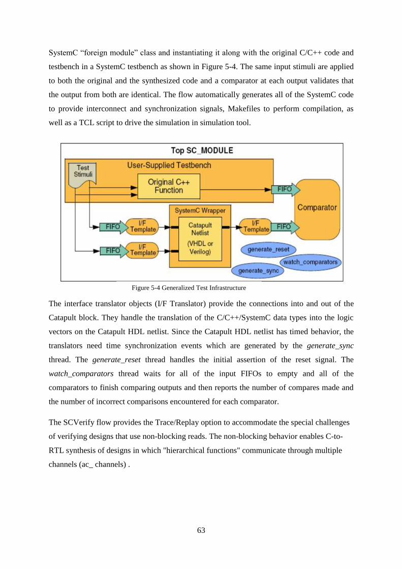
63
SystemC ―foreign module‖ class and instantiating it along with the original C/C++ code and
testbench in a SystemC testbench as shown in Figure 5-4. The same input stimuli are applied
to both the original and the synthesized code and a comparator at each output validates that
the output from both are identical. The flow automatically generates all of the SystemC code
to provide interconnect and synchronization signals, Makefiles to perform compilation, as
well as a TCL script to drive the simulation in simulation tool.
The interface translator objects (I/F Translator) provide the connections into and out of the
Catapult block. They handle the translation of the C/C++/SystemC data types into the logic
vectors on the Catapult HDL netlist. Since the Catapult HDL netlist has timed behavior, the
translators need time synchronization events which are generated by the generate_sync
thread. The generate_reset thread handles the initial assertion of the reset signal. The
watch_comparators thread waits for all of the input FIFOs to empty and all of the
comparators to finish comparing outputs and then reports the number of compares made and
the number of incorrect comparisons encountered for each comparator.
The SCVerify flow provides the Trace/Replay option to accommodate the special challenges
of verifying designs that use non-blocking reads. The non-blocking behavior enables C-to-
RTL synthesis of designs in which "hierarchical functions" communicate through multiple
channels (ac_ channels) .
Figure 5-4 Generalized Test Infrastructure
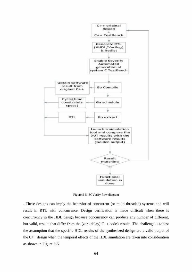
64
. These designs can imply the behavior of concurrent (or multi-threaded) systems and will
result in RTL with concurrence. Design verification is made difficult when there is
concurrency in the HDL design because concurrency can produce any number of different,
but valid, results that differ from the (zero delay) C++ code's results. The challenge is to test
the assumption that the specific HDL results of the synthesized design are a valid output of
the C++ design when the temporal effects of the HDL simulation are taken into consideration
as shown in Figure 5-5.
Figure 5-5: SCVerify flow diagram

65
The SCVerify flow now includes the new ―Trace and Replay‖ approach to verify concurrent
designs. During HDL simulation this approach traces the communication channels through
which the hierarchical blocks of the design pass data, and then replays that data as input to
the algorithmic functions of the C++ design, thus validating each block's discrete execution
with "stimulus" from the corresponding event from the HDL run, in other words the
trace/replay method can simulate how data moves from one C++ block to another with the
same values, and in the same order, as in the synthesized RTL design even when the order of
module evaluation differs from the HDL. When this is done on a correctly synthesized
design, the outputs of the C++ and RTL will match.
5.4.3 Traditional VHDL testbench
VHDL testing is in the same environment of the original RTL VHDL code .Test benches are
divided into two major components: the reusable test harness, and the test case-specific code.
All of the testbench have to interface, through an instantiation, to the same design under
verification. the testbench should be structured with a low-level layer of reusable bus-
functional models. This low level layer is common to all testbench for the design under
verification and called the test harness. Each test case would be implemented on top of these
bus-functional models, as illustrated in Figure 5-6. The test case and the harness together
form a testbench.
Many testbench share some common functionality or need for interaction with the device
under verification. Once the low-level features are verified, the repetitive nature of
communicating with the device under verification can also be abstracted into higher level
utility routines. A test case verifying the low-level read and write operations would interface
directly with the low-level bus-functional model. But once these basic operations are
Figure 5-6: Structure of a testbench with reusable bus functional model
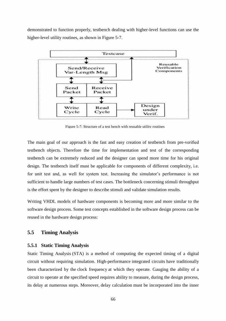
66
demonstrated to function properly, testbench dealing with higher-level functions can use the
higher-level utility routines, as shown in Figure 5-7.
The main goal of our approach is the fast and easy creation of testbench from pre-verified
testbench objects. Therefore the time for implementation and test of the corresponding
testbench can be extremely reduced and the designer can spend more time for his original
design. The testbench itself must be applicable for components of different complexity, i.e.
for unit test and, as well for system test. Increasing the simulator‘s performance is not
sufficient to handle large numbers of test cases. The bottleneck concerning stimuli throughput
is the effort spent by the designer to describe stimuli and validate simulation results.
Writing VHDL models of hardware components is becoming more and more similar to the
software design process. Some test concepts established in the software design process can be
reused in the hardware design process:
5.5 Timing Analysis
5.5.1 Static Timing Analysis
Static Timing Analysis (STA) is a method of computing the expected timing of a digital
circuit without requiring simulation. High-performance integrated circuits have traditionally
been characterized by the clock frequency at which they operate. Gauging the ability of a
circuit to operate at the specified speed requires ability to measure, during the design process,
its delay at numerous steps. Moreover, delay calculation must be incorporated into the inner
Figure 5-7: Structure of a test bench with reusable utility routines
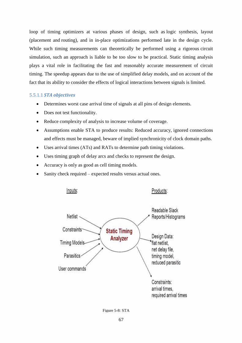
67
loop of timing optimizers at various phases of design, such as logic synthesis, layout
(placement and routing), and in in-place optimizations performed late in the design cycle.
While such timing measurements can theoretically be performed using a rigorous circuit
simulation, such an approach is liable to be too slow to be practical. Static timing analysis
plays a vital role in facilitating the fast and reasonably accurate measurement of circuit
timing. The speedup appears due to the use of simplified delay models, and on account of the
fact that its ability to consider the effects of logical interactions between signals is limited.
STA objectives 5.5.1.1
Determines worst case arrival time of signals at all pins of design elements.
Does not test functionality.
Reduce complexity of analysis to increase volume of coverage.
Assumptions enable STA to produce results: Reduced accuracy, ignored connections
and effects must be managed, beware of implied synchronicity of clock domain paths.
Uses arrival times (ATs) and RATs to determine path timing violations.
Uses timing graph of delay arcs and checks to represent the design.
Accuracy is only as good as cell timing models.
Sanity check required – expected results versus actual ones.
Figure 5-8: STA
68
Static timing analyzers build a graphical representation of the logical and circuit structure of
the chip. The arcs of the graph represent gates and wires in the design and carry delay and
slew information. The nodes of the graph represent pins on blocks, ports, convergence points
of multiple signals, and places where clock meets data. Storage elements and dynamic circuit
nodes appear as nodes in this graph. These nodes carry the test required to be performed
when clock meets data or whenever event order is important. These nodes also are used to
accumulate arrival times (AT) and required arrival times (RAT).
For timing analysis, an acyclic graph is required. Timing analyzers snip all loops of timing
arcs in the graph. All events occur within one cycle of the defined simulation clock. (AT) and
(RAT) are accumulated at every node during this traversal of the graph .Slews are also
calculated .These times are calculated for all signals, clock & data. The timing analysis
occurs when the tests that are resident at each node are applied to the AT information
collected from the graph traversal.This is then analyzed, sorted, and written out as reports.
5.5.1.1.1 Static Timing Paths
Paths begin at source pins (it may be a clock input), paths end at sink pins(outputs) and Paths
is represented as a series of segments in a timing graph.
5.5.1.1.2 The Timing Graph
5.5.1.1.2.1 Arcs
Represent the minimum and maximum input to output propagation delays and appropriate
slews for wires and logic blocks, provided in timing model per logic cell, calculated for wire
and to consider input slew, load and noise.
5.5.1.1.2.2 Checks (tests):
Exist whenever a signal arrival time is constrained by another signal's arrival (usually a
clock), they come from timing model, timing checks are implied when clock and data signals
meet, circuit functionality determines the checks – these are identified in the graph as timing
elements as clock gate, latch and flip flop.
5.5.1.1.3 Late Mode Analysis
Verify signals not to arrive too late, compares latest possible data arrival versus earliest
required time. Often conducted at typical process corner under worst PVT conditions for
yield considerations.

69
5.5.1.1.4 Validate registration
Checks that data are set up before the required time .Usually the required time is determined
by a clock, launch and capture events are derived from different real time edges of the master
clock. Slowing cycle time remedies these violations, this is not true for the rare zero cycle
setup check.
5.5.1.1.5 Early Mode Analysis (Short paths analysis)
Verify signals not to arrive too early, compares earliest possible data arrival against latest
required time, identifies potential race hazards in a design, usually between clock and data
signals. Often conducted at best process corner under best PVT conditions.
5.5.1.1.6 Validate registration
Checks that data held long enough at destination circui
5.5.2 Dynamic timing analysis
It is like the flow of functional verification except we include the technology files that
contain the time delay of the design, it‘s not like the static timing analysis, we applying a test
input vector to measure the performance and examine the timing constraints effect on the
output results. Dynamic timing analysis is based on generating and simulating a set of
patterns for sensitizing the longest paths in the circuit; it is false-path aware. However, it
requires an accurate path selection method for selecting the longest paths and a pattern
generation method.
Dynamic timing simulation take a long period of time, coverage is dependent on the quality
of the set of input vectors (Pattern dependent). Examination of logic failures not
comprehensive in analyzing problems (Incomplete coverage), it determines whether an event
will occur. Figure 5-9 shows the complete verification flow and the need of timing analysis
(static or dynamic) in an efficient design flow.
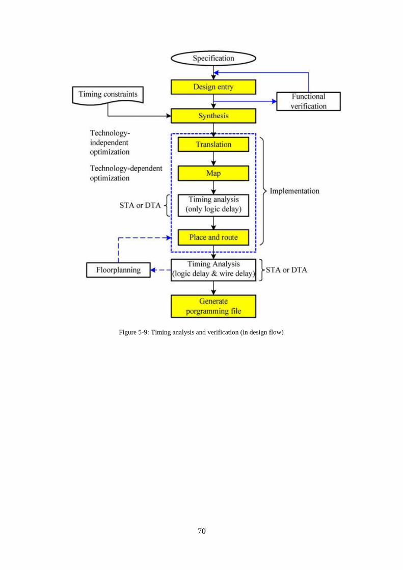
70
Figure 5-9: Timing analysis and verification (in design flow)

71
Hardware Implementation and Results Chapter 6:
6.1 FPGA Overview
FPGAs are reprogrammable silicon chips. Using prebuilt logic blocks and programmable
routing resources, you can configure these chips to implement custom hardware functionality
without ever having to pick up a breadboard or soldering iron. You develop digital computing
tasks in software and compile them down to a configuration file or bit-stream that contains
information on how the components should be wired together. In addition, FPGAs are
completely reconfigurable and instantly take on a brand new ―personality‖ when you
recompile a different configuration of circuitry
FPGA chip adoption across all industries is driven by the fact that FPGAs combine the best
parts of ASICs and processor-based systems. FPGAs provide hardware-timed speed and
reliability, but they do not require high volumes to justify the large upfront expense of custom
ASIC design. Reprogrammable silicon also has the same flexibility of software running on a
processor-based system, but it is not limited by the number of processing cores available.
Unlike processors, FPGAs are truly parallel in nature, so different processing operations do
not have to compete for the same resources. Each independent processing task is assigned to
a dedicated section of the chip, and can function autonomously without any influence from
other logic blocks. As a result, the performance of one part of the application is not affected
when you add more processing.
6.2 Advantages of FPGA design Methodologies
Once used only for glue logic, FPGAs have progressed to a point where system-on-chip
(SoC) designs can be built on a single device. The number of gates and features has increased
dramatically to compete with capabilities that have traditionally been offered through ASIC
devices only. Next we will address some of the advantages of FPGA design methodologies
over ASICs including early time-to-market, IP integration, tool support, easy transition to
structured ASICs.
72
6.2.1 Early Time to Market
As FPGA devices progressed both in terms of resources and performance, the latest FPGAs
have come to provide "platform" solutions that are easily customizable for system
connectivity, DSP, and/or data processing applications. As platform solutions are becoming
more and more important, leading FPGA vendors are coming up with easy-to-use design
development tools.
These platform building tools accelerate time-to-market by automating the system definition
and integration phases of system on programmable chip (SOPC) development. The tools not
only improve design productivity, but also reduce the cost of buying these tools from 3rd
party EDA vendors. Using such tools, system designers can define a complete system, from
hardware to software, within one tool and in a fraction of the time of traditional system-on-a-
chip (SOC) design.
6.2.2 IP Integration
With the availability of multi-million gate FPGAs, to become significantly productive, the
designer has to leverage the use of IP as much as possible. Integration of a third party IP is
not that easy to perform, as one has to verify the IP to the targeted technology and then make
sure that the IP meets the area and performance specification.
But with FPGAs, the vendors themselves take the trouble of verifying the third party and in-
house developed IP for area and performance. The biggest advantage of platform based
design is that it supports integration of proprietary logic along with third party IP.
The challenge for any system-on-a-chip FPGA is to verify the functionality of the complete
system that includes processor cores, third party IP and proprietary logic. To perform this
type of verification, along with a high speed simulator, verification engineers also need a
complete suite of verification tools. To support system verification, the FPGA design
methodology supports formal verification and static timing analysis.
6.2.3 Tool Support
FPGA design flows support the use of third party EDA tools to perform design flow tasks
such as static timing analysis, formal verification, and RTL and gate level simulation.
73
Traditionally, FPGA design and PCB design has been done separately by different design
teams using multiple EDA tools and processes. This can create board level connectivity and
timing closure challenges, which can impact both performance and time-to-market for
designers. New EDA tools bring together PCB solutions and FPGA vendor design tools,
helping enable a smooth integration of FPGAs on PCBs.
6.2.4 Transition to structured ASICs
When the demand for the FPGA parts increases, FPGA vendors provide a comprehensive
alternative to ASICs called structured ASICs that offer a complete solution from prototype to
high-volume production, and maintain the powerful features and high-performance
architecture of their equivalent FPGAs with the programmability removed. Structured ASIC
solutions not only provide performance improvement, but also result in significant cost
reduction.
With the advent of new technologies in the field of FPGAs, design houses are provided with
an option other than ASICs. With the mask costs approaching a one million dollar price tag,
and NRE costs in the neighborhood of another million dollars, it is very difficult to justify an
ASIC for a low unit volume. FPGAs, on the other hand, have improved their capacity to build
systems on a chip with more than million ASIC equivalent gates and a few megabits of on
chip RAM. For high volumes, a structured ASIC solution combines the cost advantage of
ASICs with a low risk solution of an FPGA.
6.3 Embedded System Design
Designing with FPGAs gives you the flexibility to implement some functionality in discrete
system components, some in software, and some in FPGA-based hardware.
This flexibility makes the design process more complex. The SOPC Builder system design
tool helps to manage this complexity. Even if you decide a soft-core processor doesn't meet
your application's needs, SOPC Builder can still play a vital role in your system by providing
mechanisms for peripheral expansion or processor off load.
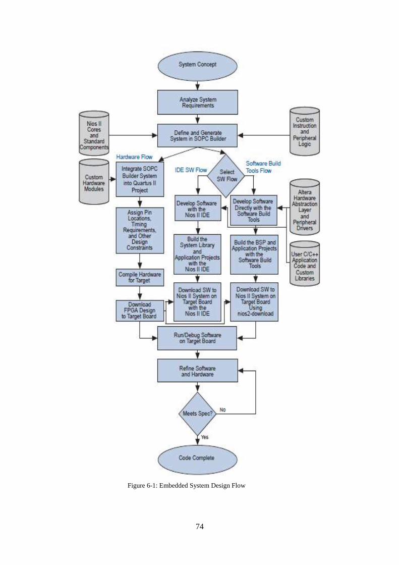
74
Figure 6-1: Embedded System Design Flow

75
6.3.1 SoPC Builder Design
SOPC Builder simplifies the task of building complex hardware systems on an FPGA. SOPC
Builder allows you to describe the topology of your system using a graphical user interface
(GUI) and then generate the hardware description language (HDL) files for that system. The
Quartus II software compiles the HDL files to create an FPGA programming file.
SOPC Builder allows you to choose the processor core type and the level of cache,
debugging, and custom functionality for each Nios II processor. Your design can use on-chip
resources such as memory, PLLs, DSP functions, and high-speed transceivers. You can
construct the optimal processor for your design using SOPC Builder.
After you construct your system using SOPC Builder, and after you add any required custom
logic to complete your top-level design, you must create pin assignments using the Quartus II
software. The FPGA‘s external pins have flexible functionality, and a range of pins is
available to connect to clocks, control signals, and I/O signals.
The design flow includes the following high-level steps:
Package your component for SOPC Builder using the Component Editor.
Simulate at the unit-level, possibly incorporating Avalon BFMs to verify the system.
Complete the SOPC Builder design by adding other components, specifying interrupts,
clocks, resets, and addresses.
Generate the SOPC Builder system.
Perform system level simulation.
Constrain and compile the design.
Download the design to an Altera device.
Test in hardware.

76
6.3.2 Software Design
This section contains brief descriptions of the software design tools provided by the Nios II
EDS, and the software build tools development flow, Check Appendix C.
Tools Description 6.3.2.1
The Nios II EDS provides the following tools for software development:
6.3.2.1.1 GNU tool chain
GCC-based compiler with the GNU binary utilities
6.3.2.1.2 Nios II processor-specific port of the newlib C library
6.3.2.1.3 Hardware abstraction layer (HAL)
The HAL provides a simple device driver interface for programs to communicate with the
underlying hardware. It provides many useful features such as a POSIX-like application
program interface (API) and a virtual-device file system.
6.3.2.1.4 Nios II IDE
The Nios II IDE is a GUI that supports creating, modifying, building, running, and debugging
Nios II programs. It is based on the Eclipse open development platform and Eclipse C/C++
development toolkit (CDT) plug-ins.
6.3.2.1.5 Nios II software build tools flow
The Nios II software build tools development flow is a scriptable, command-line based
development flow that uses the software build tools independent of the Nios II IDE.
The Nios II software development tutorial teaches you about the following key elements of
the flow:
System library project
Software abstraction of the SOPC Builder hardware design
Application project
The software that drives your application
77
Software Build Tools Flow 6.3.2.2
The Nios II software build tools flow uses the software build tools to provide a flexible,
portable, and scriptable software build environment. Altera recommends that you use this
flow if you prefer a command-line environment, or if you want a set of build tools that fits
easily in your preferred software or system development environment. The Nios II software
build tools are the basis for Altera‘s future development. The software build tools flow
requires that you have an SOPC file (.sopc) generated by SOPC Builder for your system. The
flow includes the following steps to create software for your system:
Create a board support package (BSP) for your system. The BSP is a layer of software that
interacts with your development system. It is a makefile-based project.
Create your application software:
Write your code.
Generate a makefile-based project that contains your code.
Iterate through one or both of these steps until your design is complete.
6.4 Cyclone III EP3C25 NIOS II Starter Kit
Cyclone III device family offers a unique combination of high functionality, low power and
low cost. Based on Taiwan Semiconductor Manufacturing Company (TSMC) low-power
(LP) process technology, silicon optimizations and software features to minimize power
consumption, Cyclone III device family provides the ideal solution for your high-volume,
low-power, and cost-sensitive applications. To address the unique design needs, Cyclone III
device family offers the following two variants:
Cyclone III—lowest power, high functionality with the lowest cost
Cyclone III LS—lowest power FPGAs with security separation which enables you to
introduce redundancy in a single chip to reduce size, weight, and power of your application.

78
6.4.1 The Main Features of the Cyclone III Starter board:
Low-power consumption Altera Cyclone III EP3C25 chip in a 324-pin Fine Line BGA
(FBGA) package
Expandable through HSMC connector
32-Mbyte DDR SDRAM
16-Mbyte parallel flash device for configuration and storage
1 Mbyte high-speed SSRAM memory
Four user push-button switches
Four user LEDs
Figure 6-2 Cyclone III FPGA Starter Kit

79
6.4.2 Main Advantages of the Cyclone III Starter Board
Facilitates a fast and successful FPGA design experience with helpful example designs and
demonstrations.
Directly configure and communicate with the Cyclone III device via the on-board USB-
Blaster™ circuitry and JTAG header
Active Parallel flash configuration
Low power consumption
Cost-effective modular design
6.4.3 Board Component Blocks
Altera Cyclone III EP3C25F324 FPGA 6.4.3.1
25K logic elements (LEs)
Figure 6-3: Cyclone III FPGA Starter blocks
80
66 M9K memory blocks (0.6 Mbits)
16 18x18 multiplier blocks
Four PLLs
214 I/Os
Clock management system 6.4.3.2
One 50 MHz clock oscillator to support a variety of protocols
The Cyclone III device distributes the following clocks from its on-board PLLs:
DDR clock
SSRAM clock
Flash clock
HSMC connector 6.4.3.3
Provides 12 V and 3.3 V interface for installed daughter cards
Provides up to 84 I/O pins for communicating with HSMC daughter cards
General user-interface 6.4.3.4
Four user LEDs
Two board-specific LEDs
Push-buttons:
System reset
User reset
Four general user push-buttons
Memory subsystem 6.4.3.5
6.4.3.5.1 Synchronous SRAM device
1-Mbyte standard synchronous SRAM

81
167-MHz
Shares bus with parallel flash device
6.4.3.5.2 Parallel flash device
16-Mbyte device for active parallel configuration and storage
Shares bus with SRAM device
6.4.3.5.3 DDR SDRAM device
56-pin, 32-Mbyte DDR SDRAM
167-MHz
Connected to FPGA via dedicated 16-bit bus
6.4.3.5.4 Built-in USB-Blaster interface
Using the Altera EPM3128A CPLD
For external configuration of Cyclone III device
For system debugging using the SignalTap and Nios debugging console
Communications port for Board Diagnostic graphical user interface (GUI)
6.5 NIOS II Overview
Nios II is Altera's proprietary processor targeted for its FPGA devices. It is configurable and
can be trimmed to meet specific needs. Next, we examine its basic organization and key
components. The emphasis is on the features that may affect future software and I/O
peripheral development.
6.5.1 Introduction
Nios II is a soft-core processor targeted for Altera's FPGA devices. As opposed to a fixed
prefabricated processor, a soft-core processor is described by HDL codes and then mapped
onto FPGA's generic logic cells. This approach offers more flexibility.

82
A soft-core processor can be configured and tuned by adding or removing features on a
system-by-system basis to meet performance or cost goals.
The Nios II processor follows the basic design principles of a RISC (Reduced Instruction Set
Computer) architecture and uses a small, optimized set of instructions.
Its main characteristics are:
Load-store architecture
Fixed 32-bit instruction format
32-bit internal data path
32-bit address space
Memory-mapped I/O space
32-level interrupt requests
32 general-purpose registers
The main blocks are:
Register file (general purpose registers) and control registers
ALU (arithmetic and logic unit)
Exception and interrupt handler
Optional instruction cache and data cache
Optional MMU (memory management unit)
Optional MPU (memory protection unit)
Optional JTAG debug module

83
There are three basic versions of Nios II:
Nios Il/f: The fast core is designed for optimal performance. It has a 6-stage pipeline,
instruction cache, data cache, and dynamic branch prediction.
Nios II/s: The standard core is designed for small size while maintaining good performance.
It has a 5-stage pipeline, instruction cache, and static branch prediction.
Nios Il/e: The economy core is designed for optimal size. It is not pipelined and contains no
cache.
These processors' key characteristics are summarized on the top of Table x.1 and their sizes
and performances are listed on the bottom.
Figure 6-4: The conceptual block diagram of a Nios II processor

84
Within each version, the processor can be further configured by including or excluding
certain features (such as the JTAG debugging unit) and adjusting the size and performance of
certain components (such as cache size). While the performance and size are different, the
three versions share the same instruction set. Thus, from the software programmer's point of
view, the three versions appear to be identical and the software dose not needed to be
modified for a particular core.
Although the Nios II processor is described by HDL codes, the file is encrypted and a user
cannot modify its internal organization via the codes. It should be treated as a black box that
executes the specified instructions. The main blocks of the processor are examined briefly in
following sections. The emphasis is on their impacts on applications rather than their internal
implementation.
6.5.2 Register File and ALU
Register File 6.5.2.1
A Nios II processor consists of thirty two 32-bit general-purpose registers. The register 0 is
hardwired and always returns the value zero and the register 31 is used to hold the return
address during a procedure call. The other registers are treated identical by the processor but
may be assigned for special meaning by an assembler or compiler. The processor also has
several control registers, which report the status and specify certain processor behaviors.
Since we use C language for software development in this book, these registers are not
directly referenced in codes.
Table 6-1: Comparison between NIOS II three basic versions

85
ALU 6.5.2.2
ALU operates on data stored in general-purpose registers. An ALU operation takes one or
two inputs from registers and stores a result back to a register. The relevant instructions are:
Arithmetic operations: addition, subtraction, multiplication, and division.
Logical operations: and, or, nor, and xor.
Shift operations: logic shift right and left, arithmetic shift right and left, and rotate right and
left.
Ideally, the ALU should support all these operation. However, the implementation of
multiplication, division, and variable-bit shifting operation is quite complex and requires
more hardware resources. A Nios II processor can be configured to include or exclude these
units. An instruction without hardware support is known as an "unimplemented instruction"
in Altera literature. When an unimplemented instruction is issued, the processor generates an
exception, which in turn initiates an exception handling routine to emulate the operation in
software.
6.5.3 Memory and I/O Organization
Nios II memory interface 6.5.3.1
A Nios II processor utilizes separate ports for instruction and data access. The instruction
master port fetches the instructions and performs only read operation. The data master port
reads data from memory or a peripheral in a load instruction and writes data to memory or a
peripheral in a store instruction. The two master ports can use two separate memory modules
or share one memory module
Overview of Memory Hierarchy 6.5.3.2
In an ideal scenario, a system should have a large, fast, and uniform memory, in which data
and instruction can be accessed at the speed of the processor. In reality, this is hardly
possible. Fast memory, such as the embedded memory modules within an FPGA device, is
usually small and expensive. On the other hand, large memory, such as the external SDRAM
(synchronous dynamic RAM) chip, is usually slow. One way to overcome the problem is to
organize the storage as a hierarchy and put the small, fast memory component closer to the
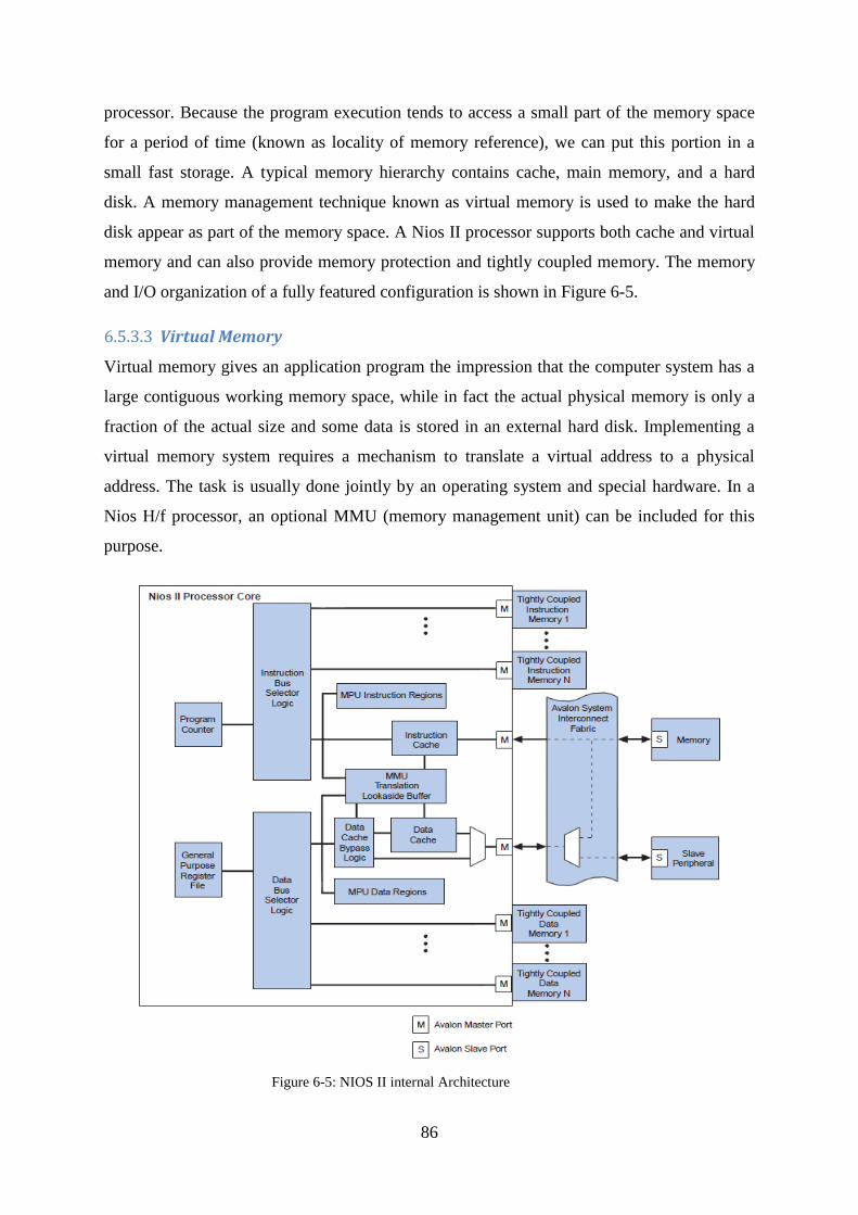
86
processor. Because the program execution tends to access a small part of the memory space
for a period of time (known as locality of memory reference), we can put this portion in a
small fast storage. A typical memory hierarchy contains cache, main memory, and a hard
disk. A memory management technique known as virtual memory is used to make the hard
disk appear as part of the memory space. A Nios II processor supports both cache and virtual
memory and can also provide memory protection and tightly coupled memory. The memory
and I/O organization of a fully featured configuration is shown in Figure 6-5.
Virtual Memory 6.5.3.3
Virtual memory gives an application program the impression that the computer system has a
large contiguous working memory space, while in fact the actual physical memory is only a
fraction of the actual size and some data is stored in an external hard disk. Implementing a
virtual memory system requires a mechanism to translate a virtual address to a physical
address. The task is usually done jointly by an operating system and special hardware. In a
Nios H/f processor, an optional MMU (memory management unit) can be included for this
purpose.
Figure 6-5: NIOS II internal Architecture
87
Memory Protection 6.5.3.4
Modern operation systems include protection mechanisms to restrict user applications to
access critical system resource. For example, some operation systems divide the program
execution into kernel mode (without restriction) and user mode (with restriction).
Implementation of this scheme also requires special hardware support. In a Nios Il/f
processor, an optional MPU (memory protection unit) can be included for this purpose. As in
MMU, a proper operation system is needed to utilize the MPU feature.
In a Nios II configuration, the use of MMU and MPU is mutually exclusive; this means that
only one of them can be included.
Cache Protection 6.5.3.5
Cache memory is a small, fast memory between the processor and main memory, as shown in
Figure 8.2. In a Nios II processor, the cache is implemented by FPGA's internal embedded
memory modules and the main memory is usually composed of external SDRAM devices. As
long as most memory accesses are within cached locations, the average access time will be
closer to the cache latency than to the main memory latency.
The operation of cache memory can be explained by a simple example. Consider the
execution of a loop segment in a large program, which resides on the main memory. The
steps are:
At the beginning, code and data are loaded from the main memory to the cache.
The loop segment is executed.
When the execution is completed, the modified data is transferred back from the cache to the
main memory.
In this process, the access time at the beginning and end is similar to the main memory
latency and the access time for loop execution is similar to the cache latency. Since a typical
loop segment iterates through the body many times, the average access time of this segment
is closer to the cache latency.
A Nios II processor can be configured to include an instruction cache or both instruction and
data cache. The sizes of the caches can be adjusted as well. Unlike MMU and MPU, no

88
special operating system feature is needed to utilize the cache. Cache simply speeds up the
average memory access time and is almost transparent to software.
Tightly Coupled Memory 6.5.3.6
Tightly coupled memory is somewhat unique to the embedded system. It is a small, fast
memory that provides guaranteed low-latency memory access for timing-critical applications.
One problem with a cache memory system is that its access time may vary. While its average
access time is improved significantly, the worst-case access time can be really large (for
example, the data is in SDRAM). Many tasks in an embedded system are time-critical and
cannot tolerate this kind of timing uncertainty.
To overcome the problem, a Nios II configuration can add additional master instruction and
data ports for tightly coupled memory. While the cache is loaded as needed and its content
changes dynamically, tightly coupled memory is allocated for a specific chunk of instruction
or data. The assignment is done at the system initialization. One common use of tightly
coupled memory is for interrupt service routines. The high-priority interrupts are frequently
critical and must be processed within a certain deadline. Putting the routines in a tightly
coupled memory removes the timing uncertainty and thus guarantees the response time.
I/O Organization 6.5.3.7
The Nios II processor uses a memory-mapped I/O method to perform input and output
between the processor and peripheral devices. An I/O device usually contains a collection of
registers for command, status, and data. In the memory-mapped I/O scheme, the processor
uses the same address space to access memory and the registers of I/O devices. Thus, the load
and store instructions used to access memory can also be used to access I/O devices.
The inclusion of a data cache may cause a problem for this scheme because I/O command
and status should not be buffered in an intermediate storage between the processor and I/O
devices. A bypass path is needed for this purpose, as implemented by a two-to-one
multiplexer in Figure 8.2. The Nios II processor introduces an additional set of load and store
instructions for this purpose. When an I/O load or store instruction is issued, the operation
bypasses the data cache and data is retrieved from or send to the master port directly.

89
Interconnect Structure 6.5.3.8
In a traditional system, the main memory module and I/O devices are connected to a
common, shared bus structure. Contention on bus sometimes becomes the bottleneck of the
system. The Nios II processor utilizes Altera's Avalon interconnect structure. The
interconnect is implemented by a collection of decoders, multiplexers, and arbitrators and
provides concurrent transfer paths.
6.5.4 Exception and Interrupt Handler
The exception and interrupt handler processes the internal exceptions and external interrupts.
The Nios II processor supports up to 32 interrupts and has 32 level sensitive interrupt request
inputs. When an exception or interrupt occurs, the processor transfers the execution to a
specific address. An interrupt service routine at this address determines the cause and takes
appropriate actions.
6.5.5 JTAG Debug Module
The debug module connects to the signals inside the processor and can take control over the
processor. A host PC can use the FPGA's JTAG port to communicate with the debug module
and perform a variety of debugging activities, such as downloading programs to memory,
setting break points, examining registers and memory, and collecting execution trace data.
The debug module can be included or excluded in the processor and its functionality can be
configured. We can include it during the development process and remove it from the final
production.

90
6.6 NIOS II in Video Processing
NOIS II plays a very important role in the video tracking algorism on the Cyclone III starter
kit as it connect all the processing blocks together and control all the memory access and In
our design we used the Video output port on the kit as an video input, Also some of built in
libraries ―Altera Video Image Processing Suite IP cores ‖ Which modified to achieve our
target such as Deinterlacer and mixer, Mean-shift block generated from the Catapult and the
VGA port and the LCD as a out ports to view the tracked video after processing
IP MegaCore
Function
Description
Frame Reader Reads video from external memory and outputs it as a stream.
Control
Synchronizer
Synchronizes the changes made to the video stream in real time between two
functions.
Switch Allows video streams to be switched in real time.
Color Space
Converter
Converts image data between varieties of different color spaces such as RGB to
YCrCb.
Chroma Resampler Changes the sampling rate of the chroma data for image frames, for example
from 4:2:2 to 4:4:4 or 4:2:2 to 4:2:0.
2D FIR Filter Implements a 3x3, 5x5, or 7x7 finite impulse response (FIR) filter on an image
data stream to smooth or sharpen images.
Scaler Allows custom scaling and real-time updates of both the image sizes and the
scaling coefficients.
Deinterlacer Converts interlaced video formats to progressive video format using a motion
adaptive deinterlacing algorithm. Also supports "bob" and "weave" algorithms.
Test Pattern
Generator
Generates a video stream that contains still color bars for use as a test pattern.
Clipper Provides a way to clip video streams and can be configured at compile time or at
run time.
Color Plane
Sequencer
Changes how color plane samples are transmitted across the Avalon-ST
interface. This function can be used to split and join video streams, giving
control over the routing of color plane samples.
Frame Buffer Buffers video frames into external RAM. This core supports double or triple-
buffering with a range of options for frame dropping and repeating.
Clocked Video Input
and Output
Convert the industry-standard clocked video format (BT-656) to Avalon-ST video
and vice versa.
6.6.1 Working Demo Procedure
Record a video using any type of camera ―assuming the tracked object is in the center of the
first frame‖ ―in our case we use IPad Camera‖.
Connect the camera to the Kit through the Video out port on the kit ―the yellow socket‖.
Table 6-2: Video and Image Processing Suite IP MegaCore Functions

91
Play the recorded video.
The tracked version the recorded video will be displayed on the LCD and through the VGA
port on any screen ―real-time processing‖.
6.6.2 System Overall Block Diagram
6.6.3 Flow Summary from Quartus
Figure 6-6: Overall system block diagram

92
Comclusion Chapter 7:
Using HLS tools proved to have many advantages:
A very fast time-to-market,
Easy C-to-RTL conversion,
Easy design space exploration
Easier automated verification flow.
However, care should be taken as the tools are not mature enough and it still have some bugs
that could result in outputs that are not as expected. Also the area and speed results generated
from the HLS tool should be computed again by a logic synthesis tool as they are only
estimation from the HLS tool. Also Hierarchal design proved to have some bugs in the tool.

93
References
[1] Daniel D.Gajski, Nikil D.Dutt, Allen C-H Wu, High – Level Synthesis Introduction to
Chip and System Design, 1st ed. Kluwer Academic publishers, 1992.
[2] Alper Ylmiz, Omar Javed, Mubarak Shah, ―Object Tracking: A Survey‖, 2006.
[3] Comaniciu, D., Ramesh, V., Meer, P., ―Real-time tracking of non-rigid objects using
mean shift‖, Proc. IEEE Conference on Computer Vision and Pattern Recognition,
Hilton Head, vol. 2, pp. 142--149 (2000).
[4] Ehsan Norouznezhad, Abbas Bigdeli, Adam Postula, Brian C. Lovell, ―Object
Tracking on FPGA-based Smart Cameras using Local Oriented Energy and Phase
Features‖.
[5] Michel Fingeroff, High – Level Synthesis Blue Book, 2010, Mentor Graphics
Corporation.
[6] Catapult C Synthesis User‘s and Reference Manual, Mentor Graphics Corporation,
November 2010.
[7] Catapult C Synthesis SystemC User‘s Guide, Mentor Graphics Corporation, November
2010.
[8] ModelSim SE Reference Manual, Mentor Graphics Corporation, November 2010.
[9] Pong P.Chu, Embedded SoPC Design with NIOS II Processor and VHDL Examples,
Wiley, 2011.
[10] Embedded Design Handbook, Altera Corporation, 2009.
[11] NIOS II Embedded Evaluation Kit User Guide, Altera Corporation, 2009.
[12] Jarnick Bergeroun, Writing TestBenches Functional Verification of HDL Models,
Kluwer Academic publishers, 2002.

94
Appendix A: Software verification using Visual C
The goal is to verify the C++ fixed point code ready to be synthesized with a high level
synthesis tool like Catapult, with the results of its equivalent floating point algorithm,
libraries of math functions, fixed point and any other libraries used by synthesis tool to
compile the fixed point algorithm should be included as a header files in the visual c project
for a successful compilation.
The verification of a fixed point C code as a software with SCverify take a long time as the
tool go to synthesizes the code first and after that it go to verify the software results with the
RTL results, now we need to verify the C code only no need to waste time in synthesizing
and to go to the verification step!
We illustrate here the main steps to do that:
1. Start a new project Visual C++>>win 32, the usual steps of creating a C++ project.
2. Create a folder that contains all the libraries needed for your fixed point code, import
it from the folder ―mgc_hls\pkgc\hls_pkgs‖ ―or ….\ccs_altera‖, any library you need
include it in your own library folder, library folder is advisable to be in the same
folder which contain you project.
3. Change the project properties, by choosing the Project Properties… menu item.
4. Choosing Configuration properties C/C++ General, in Additional include
directories set the directory of your own imported HLS library folder.
5. Include the header files you need in your project, and include them in your resource
file (The codes you need to verify it) as Fig A-1.
Fig A-1
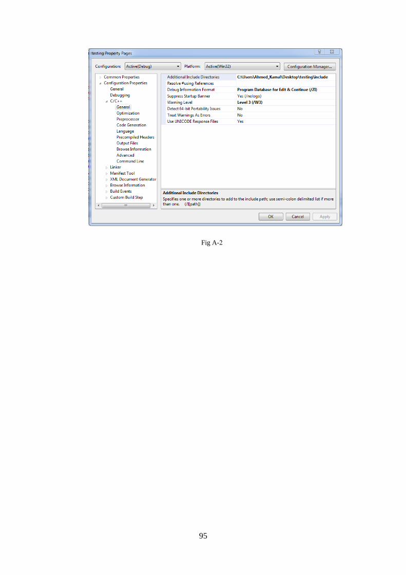
95
Fig A-2

96
Appendix B: SCVerify setting Steps
Step 1: Prepare a New Project
Preparation of a project for the SCVerify flow involves two actions:
Enabling the SCVerify Flow and Adding the C Testbench to the Input Files.
A. Enable the SystemC Verification flow either from the GUI or by entering the ―flow
package require‖ command on the Catapult command line: {flow package require
/SCVerify}. From the GUI, select the SCVerify item in the Flow Manager window.
B. Adding the C Testbench to the Input Files: The SCVerify flow needs to access the
C testbench when generating the SystemC testbench infrastructure
(mc_testbench.cpp). The best way to make the testbench accessible to the flow is to
add it to the Input Files set. However, because the testbench must not be compiled for
synthesis as part of the design, you must exclude it from compilation.
Step 2: Design Configuring the Setup Options
Configure the Setup Design options for the SCVerify flow the same way as for the basic
Catapult flow. However, you should not use of the Done Flag for process-level handshaking.
Enable the Transaction Done Signal option instead.
Step 3: Augment the
Original Testbench for
SCVerify Flow
In order to simulate the Catapult netlist
along with the execution of the original
function, you must add some code to
utilize the SCVerify infrastructure to
capture the input stimuli, call the
original function to calculate the golden
output values, and capture these outputs
Fig A-3:Testbench of a function (Cubed) of a one
input s-idx & one output s_idx_cubed
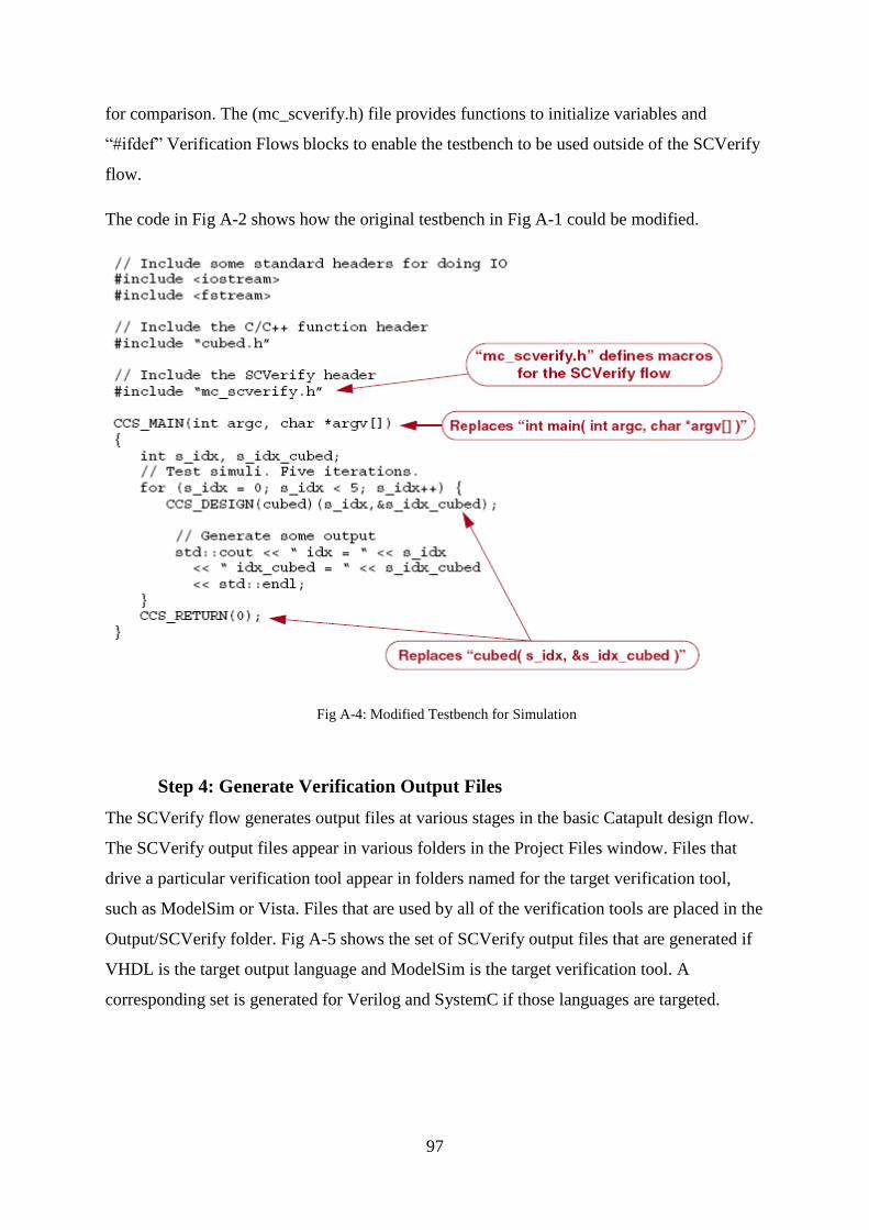
97
for comparison. The (mc_scverify.h) file provides functions to initialize variables and
―#ifdef‖ Verification Flows blocks to enable the testbench to be used outside of the SCVerify
flow.
The code in Fig A-2 shows how the original testbench in Fig A-1 could be modified.
Step 4: Generate Verification Output Files
The SCVerify flow generates output files at various stages in the basic Catapult design flow.
The SCVerify output files appear in various folders in the Project Files window. Files that
drive a particular verification tool appear in folders named for the target verification tool,
such as ModelSim or Vista. Files that are used by all of the verification tools are placed in the
Output/SCVerify folder. Fig A-5 shows the set of SCVerify output files that are generated if
VHDL is the target output language and ModelSim is the target verification tool. A
corresponding set is generated for Verilog and SystemC if those languages are targeted.
Fig A-4: Modified Testbench for Simulation

98
The Verification folder contains separate subfolders for each downstream tool supported by
the flow. Each subfolder contains makefiles to drive the corresponding verification tool. For
simulation, four tools are supported, ModelSim/QuestaSim, OSCI, NCSim, VCS and Vista.
Verification Makefiles list
a. Original Design + Testbench
Use this makefile to verify that your modified C++ testbench and your C++ design will
compile and execute correctly in the SCVerify environment. This Makefile does not simulate
any Catapult output. It only checks your C++ testbench.
b. Cycle <hdl_format> output „cycle.<hdl_ext>‟ vs Untimed C++
Fig A-5:SCVerify Flow VHDL Output Files for ModelSim Simulator

99
This is a makefile that will compile and execute the simulation for comparing your original
design to the <hdl_format> cycle model. It handles the creation of work libraries, compilation
of VHDL/Verilog cycle-accurate netlist and SystemC files, and either batch or interactive
simulation of the system.
c. RTL <hdl_format> output „rtl.<hdl_ext>‟ vs Untimed C++
This is a makefile that will compile and execute the simulation for comparing your original
design to the <hdl_format> RTL model. It handles the creation of work libraries, compilation
of VHDL/Verilog RTL netlist and SystemC files, and either batch or interactive simulation of
the system.
d. Mapped <hdl_format> output „rtl.<hdl_ext>‟ vs Untimed C++
This is a makefile hat will run the Precision RTL Synthesis tool and then simulate the original
design vs. the technology mapped netlist generated by Precision.
e. Gate <hdl_format> output „rtl.<hdl_ext>‟ vs Untimed C++
This is a makefile that will run Precision and (Altera or Xilinx) PNR and then simulate the
original design versus the(Altera or Xilinx )post-PNR netlist.
Step 5: Launch Simulation from Makefile
For this sample session, we double-click on ―RTL VHDL output „rtl.vhdl‟ vs Untimed
C++‖in the Verification/ModelSim folder. The makefile commands appear in the Catapult
transcript window, then a ModelSim session is opened and the design is loaded.
Elements of the Testbench
Typically you will start with a simple testbench that exercises the original C/C++ function
like the one in Fig A-3. Extending such a testbench to cover both the original and synthesized
designs is an easy three-step process:
1. Include the auto-generated testbench header mc_testbench.h Place #include
“mc_testbench.h” at the top of your ―testbench.cpp‖ file. If you are using SystemC data
types, it is also a good idea to include that header file just before the ―mc_testbench.h‖ header
file. The “mc_testbench.h” includes the top function of the tested design.

100
2. Capture the input stimuli for each input port
The SCVerify flow will automatically create special functions for capturing data values, one
function for each input (and output). These functions can be found in the ―mc_testbench.h‖
file and have their named derived from the formal name of the function argument which is to
be captured. Referring to Fig A-2, the input to the function ―idx‖ can be captured using the
auto-generated function named ―capture_idx().‖ The capture function has the same data type
as the original function argument and will handle the details of capturing both scalar values
and array structures. Simply insert the call to each appropriate capture_X() function, passing
in the variable that you will also pass to the original function.
3. Capture the golden output value from the original C/C++ function
Just as with the input function arguments, special capture_X() functions are created for
capturing the outputs. In Fig A-2, the correct golden value returned by the original C/C++
function is captured and placed in the FIFO by calling:
capture_idx_cubed(&s_idx_cubed);
Note that this must be done after calling the original function. If the you passed a pointer to
the variable when calling the original function, you must likewise pass the pointer to the
capture_X() function.If your design returns a value from the top function call, that output
value should be captured as well. The capture function will be derived from the name of the
function as: "capture_<function name>_out()".
Steps for post place and route timing simulation
Step1: Logic synthesis with Precision RTL
Open a new project in (Precision RTL ) ,from option >>output file>>Enable EDIF
file.
Add the ―concat_rtl.vhdl‖ to input file.
Open setup design >>choose the Technology ,Device type define the clock
frequency,etc.
Press Compile preceded by a Synthesis
Run Quartus II from the Precision RTL tool.
Go to the precision project directory >> you find a .qpf file(Quartus project).
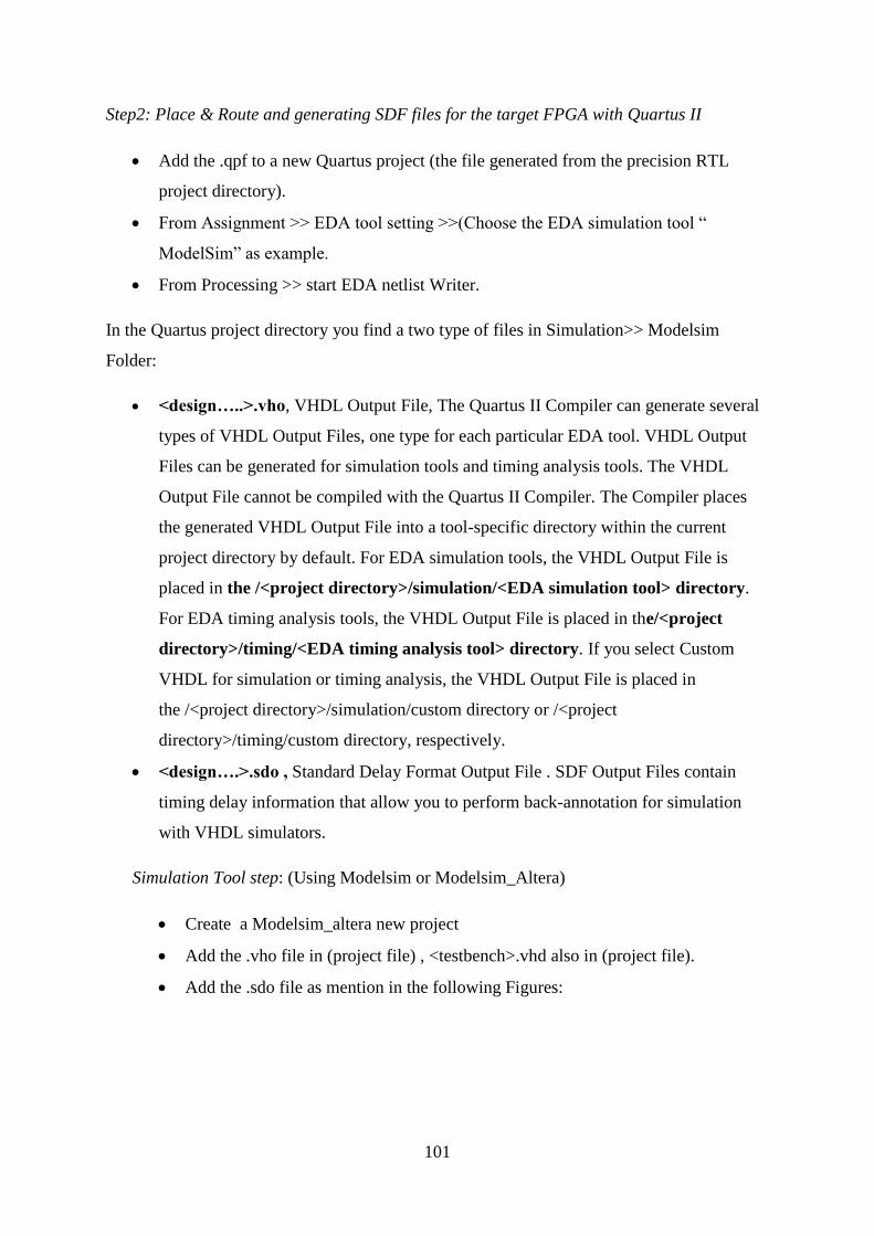
101
Step2: Place & Route and generating SDF files for the target FPGA with Quartus II
Add the .qpf to a new Quartus project (the file generated from the precision RTL
project directory).
From Assignment >> EDA tool setting >>(Choose the EDA simulation tool ―
ModelSim‖ as example.
From Processing >> start EDA netlist Writer.
In the Quartus project directory you find a two type of files in Simulation>> Modelsim
Folder:
<design…..>.vho, VHDL Output File, The Quartus II Compiler can generate several
types of VHDL Output Files, one type for each particular EDA tool. VHDL Output
Files can be generated for simulation tools and timing analysis tools. The VHDL
Output File cannot be compiled with the Quartus II Compiler. The Compiler places
the generated VHDL Output File into a tool-specific directory within the current
project directory by default. For EDA simulation tools, the VHDL Output File is
placed in the /<project directory>/simulation/<EDA simulation tool> directory.
For EDA timing analysis tools, the VHDL Output File is placed in the/<project
directory>/timing/<EDA timing analysis tool> directory. If you select Custom
VHDL for simulation or timing analysis, the VHDL Output File is placed in
the /<project directory>/simulation/custom directory or /<project
directory>/timing/custom directory, respectively.
<design….>.sdo , Standard Delay Format Output File . SDF Output Files contain
timing delay information that allow you to perform back-annotation for simulation
with VHDL simulators.
Simulation Tool step: (Using Modelsim or Modelsim_Altera)
Create a Modelsim_altera new project
Add the .vho file in (project file) , <testbench>.vhd also in (project file).
Add the .sdo file as mention in the following Figures:
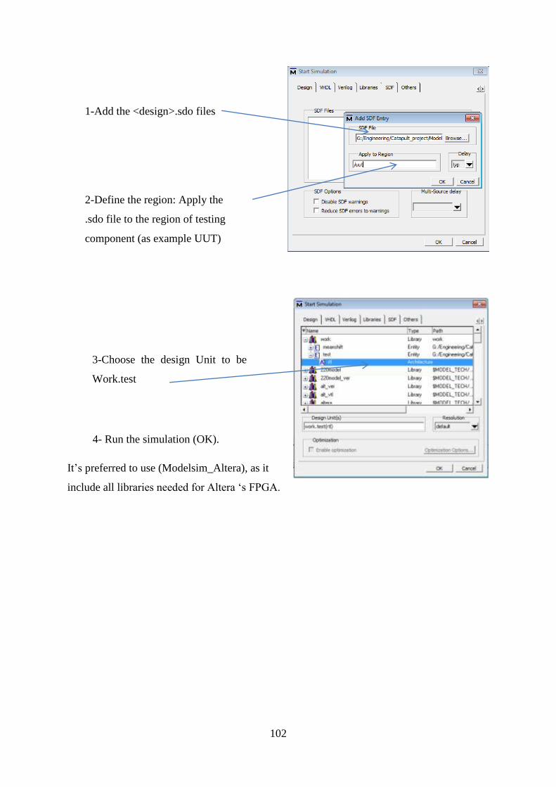
102
4- Run the simulation (OK).
It‘s preferred to use (Modelsim_Altera), as it
include all libraries needed for Altera ‗s FPGA.
1-Add the <design>.sdo files
2-Define the region: Apply the
.sdo file to the region of testing
component (as example UUT)
3-Choose the design Unit to be
Work.test
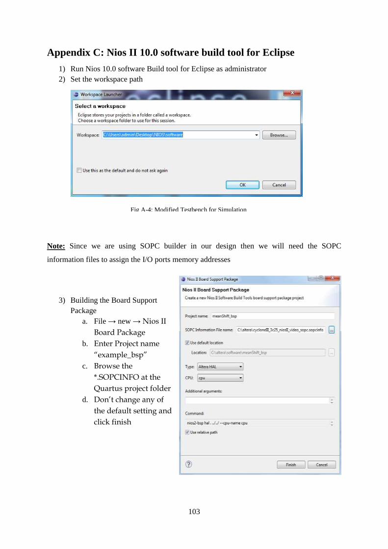
103
Appendix C: Nios II 10.0 software build tool for Eclipse
1) Run Nios 10.0 software Build tool for Eclipse as administrator
2) Set the workspace path
Note: Since we are using SOPC builder in our design then we will need the SOPC
information files to assign the I/O ports memory addresses
3) Building the Board Support
Package
a. File → new → Nios II
Board Package
b. Enter Project name
“example_bsp”
c. Browse the
*.SOPCINFO at the
Quartus project folder
d. Don’t change any of
the default setting and
click finish
Fig A-4: Modified Testbench for Simulation

104
4) Building the Application
a. File → new → Nios II
Application
b. Enter Project name
―example_test‖
c. Browse for the BSP location
―the one you previously
created (example_bsp)‖
d. Don’t change any of the
default setting and click
finish.
5) Include the application files
a. Right click on the application
folder → Import → General
→ File System
b. Browse for the (*.c, *.h,
*.cpp, *.hpp) files that you
want to include in your
application
c. Don’t change any of the
default setting and click
finish.

105
6) Compiling & Building the
project
a. Project → Build All
b. It will run for a while
and if no error “*.elf
will be generated”
7) Running Hardware
a. Right click on the
application folder →
Run As → Nios II
hardware
b. Click Run.
c. The Hardware
simulation will start
running (if no error).