an 210 effective esd protection design at system level
TRANSCRIPT
RF and Protect ion Devices
AN 210
Effective ESD Protection Design at System Level
Using VF-TLP Characterization Methodology
Application NoteRevision: 1.3 - December 6, 2012
Edition December 6, 2012
Published byInfineon Technologies AG81726 Munich, Germany
c©2012 Infineon Technologies AGAll Rights Reserved.
Legal Disclaimer
The information given in this document shall in no event be regarded as a guarantee of conditions or characteristics.With respect to any examples or hints given herein, any typical values stated herein and/or any information regardingthe application of the device, Infineon Technologies hereby disclaims any and all warranties and liabilities of any kind,including without limitation, warranties of non-infringement of intellectual property rights of any third party.
Information
For further information on technology, delivery terms and conditions and prices, please contact the nearest InfineonTechnologies Office (www.infineon.com).
Warnings
Due to technical requirements, components may contain dangerous substances. For information on the types inquestion, please contact the nearest Infineon Technologies Office.
Infineon Technologies components may be used in life-support devices or systems only with the express writtenapproval of Infineon Technologies, if a failure of such components can reasonably be expected to cause the failure ofthat life-support device or system or to affect the safety or effectiveness of that device or system. Life support devicesor systems are intended to be implanted in the human body or to support and/or maintain and sustain and/or protecthuman life. If they fail, it is reasonable to assume that the health of the user or other persons may be endangered.
Application Note No. 210
Contents
Contents
1 Introduction 51.1 Definition of Electrostatic Discharge and Electrical Overstress . . . . . . . . . . . . . . . . . . . . . . . 51.2 The IEC61000-4-2 ESD Standard . . . . . . . . . . . . . . . . . . . . . . . . . . . . . . . . . . . . . . 51.3 The IEC 61000-4-5 Surge Immunity Standard . . . . . . . . . . . . . . . . . . . . . . . . . . . . . . . . 6
1.3.1 Surge Test Measurement Setup . . . . . . . . . . . . . . . . . . . . . . . . . . . . . . . . . . . 71.4 Comparison of Component Level and System Level ESD . . . . . . . . . . . . . . . . . . . . . . . . . 8
2 Characterization of ESD Protection Devices and Circuits with a Transmission Line Pulse System 92.1 Pulsed Device Characterisation . . . . . . . . . . . . . . . . . . . . . . . . . . . . . . . . . . . . . . . . 92.2 The Transmission Line Pulse Generator . . . . . . . . . . . . . . . . . . . . . . . . . . . . . . . . . . . 10
2.2.1 How the Pulse is Generated . . . . . . . . . . . . . . . . . . . . . . . . . . . . . . . . . . . . . . 102.3 The TLP Measurement System . . . . . . . . . . . . . . . . . . . . . . . . . . . . . . . . . . . . . . . . 11
2.3.1 Discrete Voltage and Current Sensors . . . . . . . . . . . . . . . . . . . . . . . . . . . . . . . . 122.3.2 Remote Voltage and Current Sensing . . . . . . . . . . . . . . . . . . . . . . . . . . . . . . . . 122.3.3 Error Sources . . . . . . . . . . . . . . . . . . . . . . . . . . . . . . . . . . . . . . . . . . . . . . 13
2.4 Measurement Techniques . . . . . . . . . . . . . . . . . . . . . . . . . . . . . . . . . . . . . . . . . . . 132.4.1 Four Point Kelvin TLP Method . . . . . . . . . . . . . . . . . . . . . . . . . . . . . . . . . . . . . 132.4.2 Four Point Kelvin Very Fast TLP Method . . . . . . . . . . . . . . . . . . . . . . . . . . . . . . . 132.4.3 Reverse Recovery Time of Diodes . . . . . . . . . . . . . . . . . . . . . . . . . . . . . . . . . . 142.4.4 Safe Operating Area . . . . . . . . . . . . . . . . . . . . . . . . . . . . . . . . . . . . . . . . . . 162.4.5 System Level ESD Test (HMM) . . . . . . . . . . . . . . . . . . . . . . . . . . . . . . . . . . . . 16
2.5 Typical TLP Parameter . . . . . . . . . . . . . . . . . . . . . . . . . . . . . . . . . . . . . . . . . . . . . 162.6 Typical TLP Measurement Results . . . . . . . . . . . . . . . . . . . . . . . . . . . . . . . . . . . . . . 16
2.6.1 DC Sweep and Spot Leakage Measurement . . . . . . . . . . . . . . . . . . . . . . . . . . . . 162.6.2 TLP Characteristic . . . . . . . . . . . . . . . . . . . . . . . . . . . . . . . . . . . . . . . . . . . 162.6.3 Definition of the Dynamic Resistance . . . . . . . . . . . . . . . . . . . . . . . . . . . . . . . . . 172.6.4 Transient Overshoot and Clamping Voltage . . . . . . . . . . . . . . . . . . . . . . . . . . . . . 17
2.7 How TLP fits to IEC 61000-4-2 ? . . . . . . . . . . . . . . . . . . . . . . . . . . . . . . . . . . . . . . . 182.7.1 TLP Parameter Set Recomendation . . . . . . . . . . . . . . . . . . . . . . . . . . . . . . . . . 18
2.8 ESD Design . . . . . . . . . . . . . . . . . . . . . . . . . . . . . . . . . . . . . . . . . . . . . . . . . . . 182.8.1 Design Consideration . . . . . . . . . . . . . . . . . . . . . . . . . . . . . . . . . . . . . . . . . 192.8.2 PCB Layout Consideration . . . . . . . . . . . . . . . . . . . . . . . . . . . . . . . . . . . . . . 19
2.9 Conclusion . . . . . . . . . . . . . . . . . . . . . . . . . . . . . . . . . . . . . . . . . . . . . . . . . . . 20
3 Comparison of ESD Protection Technologies: Silicon Transient Voltage Suppressor (TVS) Diodes ver-sus Multilayer Varistors (MLV) 213.1 DC Sweep . . . . . . . . . . . . . . . . . . . . . . . . . . . . . . . . . . . . . . . . . . . . . . . . . . . 213.2 Dynamic Resistance . . . . . . . . . . . . . . . . . . . . . . . . . . . . . . . . . . . . . . . . . . . . . . 223.3 Transient Overshoot and Clamping Voltage . . . . . . . . . . . . . . . . . . . . . . . . . . . . . . . . . 233.4 Spot Leakage Drift . . . . . . . . . . . . . . . . . . . . . . . . . . . . . . . . . . . . . . . . . . . . . . . 243.5 Breakdown Voltage Drift . . . . . . . . . . . . . . . . . . . . . . . . . . . . . . . . . . . . . . . . . . . . 243.6 Degradation due to Multi-Pulse Stress . . . . . . . . . . . . . . . . . . . . . . . . . . . . . . . . . . . . 25
3.6.1 Spot Leakage Drift . . . . . . . . . . . . . . . . . . . . . . . . . . . . . . . . . . . . . . . . . . . 253.6.2 Breakdown Voltage Drift . . . . . . . . . . . . . . . . . . . . . . . . . . . . . . . . . . . . . . . . 26
References 27
Author 28
Copyright Notice 28
Application Note Page 3 of 29 Rev. 1.3 - December 6, 2012
Application Note No. 210
Contents
Revision History
Document No.: AN210.pdf
Revision History: December 6, 2012, Rev. 1.3
Previous Version: 1.1
Page Subjects (major changes since last revision)
All Extended release
Trademarks of Infineon Technologies AG
AURIXTM, BlueMoonTM, COMNEONTM, C166TM, CROSSAVETM, CanPAKTM, CIPOSTM, CoolMOSTM, CoolSETTM,CORECONTROLTM, DAVETM, EasyPIMTM, EconoBRIDGETM, EconoDUALTM, EconoPACKTM, EconoPIMTM, EiceDRIVERTM,EUPECTM, FCOSTM, HITFETTM, HybridPACKTM, ISOFACETM, I2RFTM, IsoPACKTM, MIPAQTM, ModSTACKTM, my-dTM,NovalithICTM, OmniTuneTM, OptiMOSTM, ORIGATM, PROFETTM, PRO-SILTM, PRIMARIONTM, PrimePACKTM, RASICTM,ReverSaveTM, SatRICTM, SIEGETTM, SINDRIONTM, SMARTiTM, SmartLEWISTM, TEMPFETTM, thinQ!TM, TriCoreTM,TRENCHSTOPTM, X-GOLDTM, XMMTM, X-PMUTM, XPOSYSTM.
Other Trademarks
Advance Design SystemTM (ADS) of Agilent Technologies, AMBATM, ARMTM, MULTI-ICETM, PRIMECELLTM, REALVIEWTM,THUMBTM of ARM Limited, UK. AUTOSARTM is licensed by AUTOSAR development partnership. BluetoothTM of BluetoothSIG Inc. CAT-iqTM of DECT Forum. COLOSSUSTM, FirstGPSTM of Trimble Navigation Ltd. EMVTM of EMVCo, LLC (VisaHoldings Inc.). EPCOSTM of Epcos AG. FLEXGOTM of Microsoft Corporation. FlexRayTM is licensed by FlexRay Consortium.HYPERTERMINALTM of Hilgraeve Incorporated. IECTM of Commission Electrotechnique Internationale. IrDATM of Infrared DataAssociation Corporation. ISOTM of INTERNATIONAL ORGANIZATION FOR STANDARDIZATION. MATLABTM of MathWorks,Inc. MAXIMTM of Maxim Integrated Products, Inc. MICROTECTM, NUCLEUSTM of Mentor Graphics Corporation. MifareTM ofNXP. MIPITM of MIPI Alliance, Inc. MIPSTM of MIPS Technologies, Inc., USA. muRataTM of MURATA MANUFACTURING CO.,MICROWAVE OFFICETM (MWO) of Applied Wave Research Inc., OmniVisionTM of OmniVision Technologies, Inc. OpenwaveTM
Openwave Systems Inc. RED HATTM Red Hat, Inc. RFMDTM RF Micro Devices, Inc. SIRIUSTM of Sirius Sattelite Radio Inc.SOLARISTM of Sun Microsystems, Inc. SPANSIONTM of Spansion LLC Ltd. SymbianTM of Symbian Software Limited. TAIYOYUDENTM of Taiyo Yuden Co. TEAKLITETM of CEVA, Inc. TEKTRONIXTM of Tektronix Inc. TOKOTM of TOKO KABUSHIKIKAISHA TA. UNIXTM of X/Open Company Limited. VERILOGTM, PALLADIUMTM of Cadence Design Systems, Inc. VLYNQTM ofTexas Instruments Incorporated. VXWORKSTM, WIND RIVERTM of WIND RIVER SYSTEMS, INC. ZETEXTM of Diodes ZetexLimited.
Last Trademarks Update 2010-06-09
Application Note Page 4 of 29 Rev. 1.3 - December 6, 2012
Application Note No. 210
1.2 The IEC61000-4-2 ESD Standard
1 Introduction
In today’s highly competitive markets, efficient ESD pro-tection has became an integral part of IC/ASIC designfor system reliability. Field failures due to ESD will be per-ceived as poor quality by disappointed customers and willincrease the number of warranty returns. Overlooking theESD problem can seriously impact company’s image andits profitability.
Reliable circuit protection following IEC61000-4-2 in-dustry’s standard is usually accomplished by the imple-mentation of ESD protection devices at critical pins. How-ever, some traditional approaches still rely on trial-and er-ror practices to design for ESD protection. This can re-quire several re-design loops until the ESD problem is fi-nally solved, for instance during compliance testing, prac-tice that increases costs and delay the time-to market ofnew electronic products.
The introduction of Very-Fast Transmission Line Pulse(vf-TLP) as support method is of utmost importance inthe selection of appropriate ESD protection devices andmakes the trial and error practices not longer justified.The Very Fast Transmission Line Pulse employs high cur-rent testing to determine the behaviour of devices and cir-cuits in the current and time domain of ESD events. Thisstrategy implemented at an early circuit design stage de-livers a faster, precise and least costly approach to im-prove ESD robustness at system level while respondingto today’s market dynamics.
The purpose of this application note is to provide theguidelines for optimized selection of protection deviceswith the support of vf-TLP. Chapter 1 provides an in-troduction to electrostatic discharge standards typicallyused in the industry. Chapter 2 describes the charac-teristics of TLP equipment as well as measurement setup and testing capabilities. Section 2.6.2 explains thetypical I/V characteristic curves of unidirectional and bidi-rectional protection devices. Chapter 3 displays a bench-mark comparison of ESD protection devices based on dif-ferent technologies, namely Multilayer Varistor (ceramictechnology) and TVS diode (silicon based technology).
1.1 Definition of Electrostatic Dischargeand Electrical Overstress
Electrostatic Discharge (ESD) is known as transfer ofelectrostatic charge between bodies or surfaces atdifferent electrostatic potential. ESD can happen dueto sudden discharge of a charged body, tribo-electricand induced charging. ESD is a high current eventin the typical range of 0.1 to 30 Apeak in a very shortperiod of time from 1 ns to 200 ns.
Electrical Overstress (EOS) is considered as the expo-sure of a device or an integrated circuit (IC) to a cur-rent or voltage beyond its absolute maximum ratings.
EOS can occur due to voltage overshoots resulting inhigh destructive currents.
ESD is considered as a subset of EOS. But EOS maycaused also by a wrong application of the IC beyond itsabsolute maximum voltage or current ratings. In this casethe damage of the IC may not happened due to an ESDevent.
The International Electrotechnical Commission (IEC)has developed transient immunity standards which havebecome minimum requirements for original equipmentmanufacturers. The basic standards for immunity testingare known as the IEC 61000-4-X standards. Three of theIEC standards deal with transient immunity:
• IEC 61000-4-2 : Electrostatic Discharge (ESD)
• IEC 61000-4-4 : Electrical Fast Transient/Burst (EFT)
• IEC 61000-4-5 : Surge Immunity
IEC 61000-4-2 is related to ESD immunity [1]. IEC 61000-4-4 and IEC 61000-4-5 are related to transient immunity[2, 3].
1.2 The IEC61000-4-2 ESD Standard
The IEC 61000-4-2 standard [1] addresses ESD tran-sients in electronic systems. It defines immunity require-ments for ESD which can be coupled into the equipment,systems or system boards directly or through radiation(air discharge). Direct coupling includes any user acces-sible entry points such as connectors, I/O ports, switches,computer keyboards, panel displays, touch screens andequipment housings.
Radiated coupling results from the spark discharge be-tween two bodies which are external to the system. Be-cause the human body is one of the most common ESDgenerators, the IEC standard defines a test set up whichsimulates an ESD event from a human body.The Human Body Model is considered as a valid repre-sentation of worst case ESD stress. Discharge into equip-ment may be through direct contact (contact dischargemethod) or just prior to contact (air discharge method).Contact discharge is the usually preferred test method,but air discharge is used where contact discharge cannotbe applied.
The ESD threat is divided into four threat levels de-pending on material and ambient humidity, as shown inTab. 1. Threat level 1 is considered the least severe whilethreat level 4 is the most severe. Levels 1 & 2 are re-served for equipment which is installed in a controlledenvironment and in the presence of antistatic materials.Level 3 is used for equipment which is sparsely but notcontinuously handled. Level 4 is required for any equip-ment which is continuously handled.
Application Note Page 5 of 29 Rev. 1.3 - December 6, 2012
Application Note No. 210
1.3 The IEC 61000-4-5 Surge Immunity Standard
Relative Antistatic Synthetic Maximum Test Voltage Test VoltageClass Humidity Material Material Charge (Contact- (Air-
(as low as) Voltage Discharge) Discharge)1 35 % x 2 kV 2 kV 2 kV2 10 % x 4 kV 4 kV 4 kV3 50 % x 8 kV 6 kV 8 kV4 10 % x 15 kV 8 kV 15 kV
Table 1: IEC 61000-4-2 severity levels and test voltages.
Indicated First Peak Current Risetime Current CurrentLevel Voltage of Discharge with Discharge at 30 ns at 60 ns
(±10 %) Switch (±30 %) (±30 %)1 2 kV 7.5 A 0.7 ns to 1 ns 4 A 2 A2 4 kV 15 A 0.7 ns to 1 ns 8 A 4 A3 6 kV 22.5 A 0.7 ns to 1 ns 12 A 6 A4 8 kV 30 A 0.7 ns to 1 ns 16 A 8 A
Table 2: IEC 61000-4-2 ESD current waveform parameters.
−50 0 50 100 150 2000
1
2
3
4
5
6
7
8
9
Time (ns)
ES
D−C
urre
nt (A
)
First Peak Current
0.7
ns -
1 ns
Ris
etim
e
10 %
90 %
I at 30 ns
I at 60 ns
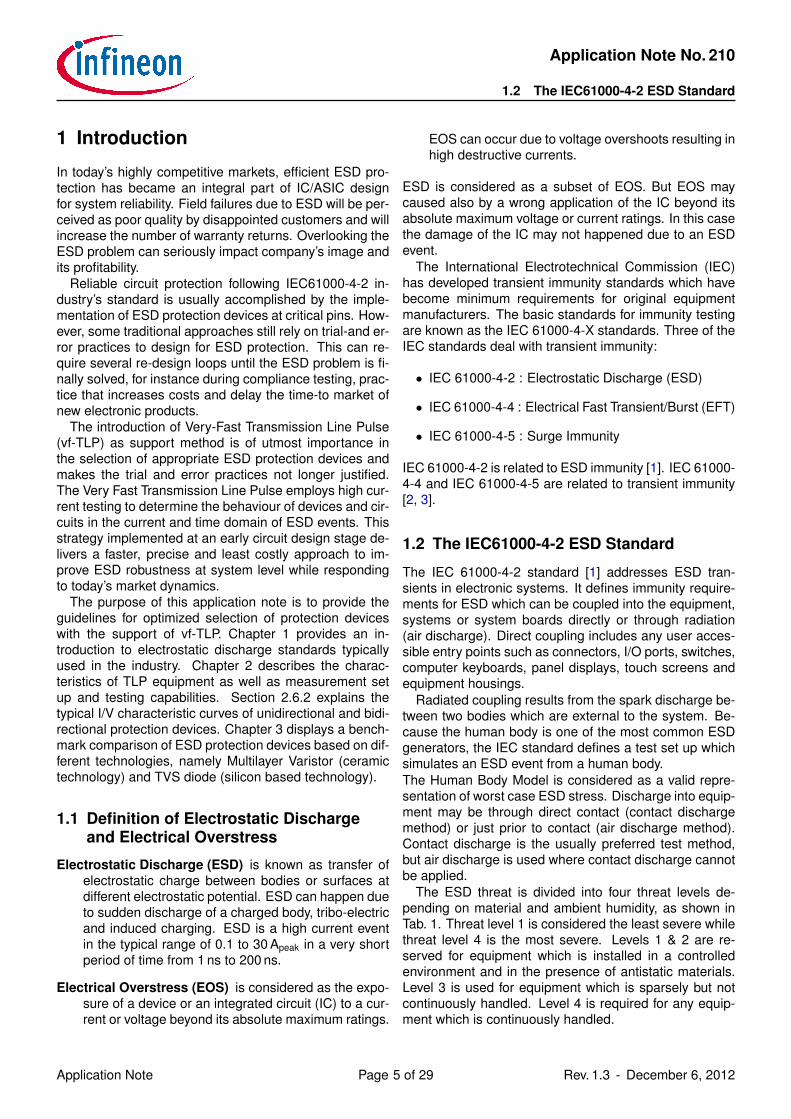
Figure 1: 2 kV ESD current pulse waveform accordingIEC 61000-4-2 (R=330Ω, C=150 pF) [1]
Fig. 1 shows a 2 kV ESD current pulse waveform ac-cording IEC 61000-4-2 with a R=330Ω and C=150 pF dis-charge circuitry. The ESD current waveform at a certainindicated discharge voltage is specified with 4 parameters(Tab. 2):
1. rise time 0.7 - 1 ns
2. first peak current of discharge (±10 %)
3. Current at 30 ns (±30 %)
4. Current at 60 ns (±30 %)
1.3 The IEC 61000-4-5 Surge ImmunityStandard
IEC 61000-4-5 addresses the most severe transient con-ditions on both power and data lines. These are tran-sient caused by lightning strikes and switching. Switchingtransients may be the result of power system switching,load changes in power distribution systems, or short cir-cuit fault conditions. Lightning transients may result froma direct strike or induced voltages and currents due to anindirect strike.
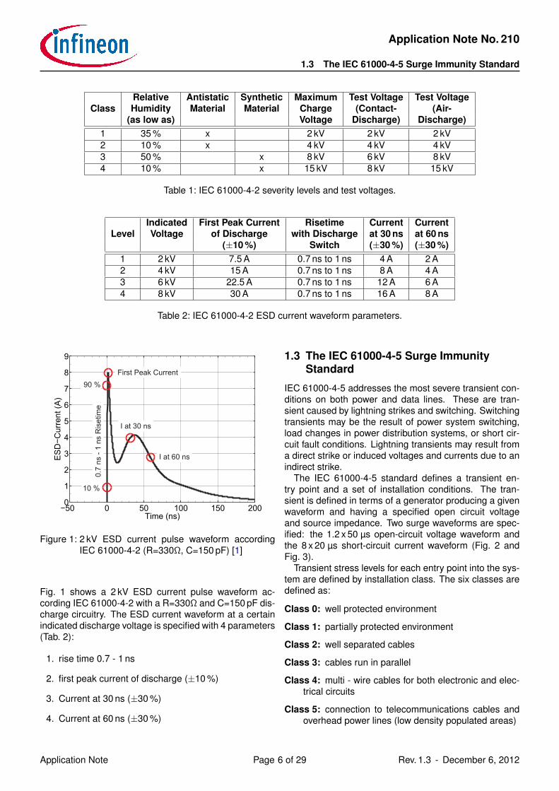
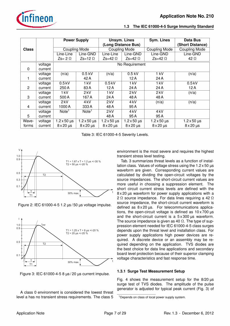
The IEC 61000-4-5 standard defines a transient en-try point and a set of installation conditions. The tran-sient is defined in terms of a generator producing a givenwaveform and having a specified open circuit voltageand source impedance. Two surge waveforms are spec-ified: the 1.2 x 50 µs open-circuit voltage waveform andthe 8 x 20 µs short-circuit current waveform (Fig. 2 andFig. 3).
Transient stress levels for each entry point into the sys-tem are defined by installation class. The six classes aredefined as:
Class 0: well protected environment
Class 1: partially protected environment
Class 2: well separated cables
Class 3: cables run in parallel
Class 4: multi - wire cables for both electronic and elec-trical circuits
Class 5: connection to telecommunications cables andoverhead power lines (low density populated areas)
Application Note Page 6 of 29 Rev. 1.3 - December 6, 2012
Application Note No. 210
1.3 The IEC 61000-4-5 Surge Immunity Standard
Power Supply Unsym. Lines Sym. Lines Data Bus(Long Distance Bus) (Short Distance)
Class Coupling Mode Coupling Mode Coupling Mode Coupling ModeLine-Line Line-GND Line-Line Line-GND Line-GND Line-GNDZs= 2 Ω Zs=12 Ω Zs=42 Ω Zs=42 Ω Zs=42 Ω 42 Ω
voltage No Requirement0 current
voltage (n/a) 0.5 kV (n/a) 0.5 kV 1 kV (n/a)1 current 42 A 12 A 24 A
voltage 0.5 kV 1 kV 0.5 kV 1 kV 1 kV 0.5 kV2 current 250 A 83 A 12 A 24 A 24 A 12 A
voltage 1 kV 2 kV 1 kV 2 kV 2 kV (n/a)3 current 500 A 167 A 24 A 48 A 48 A
voltage 2 kV 4 kV 2 kV 4 kV (n/a) (n/a)4 current 1000 A 333 A 48 A 95 A
voltage Note1 Note1 2 kV 4 kV 4 kV5 current 48 A 95 A 95 A
Wave- voltage 1.2 x 50 µs 1.2 x 50 µs 1.2 x 50 µs 1.2 x 50 µs 1.2 x 50 µs 1.2 x 50 µsforms current 8 x 20 µs 8 x 20 µs 8 x 20 µs 8 x 20 µs 8 x 20 µs 8 x 20 µs
Table 3: IEC 61000-4-5 Severity Levels.
1.0
0.9
0.5
0.3
0.1
T1
T t
V
T2
30% max.
T1 = 1.67 x T = 1.2 µs +/-30 %T2 = 50 µs +/-20 %
Figure 2: IEC 61000-4-5 1.2 µs / 50 µs voltage impulse.
1.0
0.9
0.5
0.1
T1
T t
I
IPP
T2
30% max.
T1 = 1.25 x T = 8 µs +/-20 %T2 = 20 µs +/-20 %
Figure 3: IEC 61000-4-5 8 µs / 20 µs current impulse.
A class 0 environment is considered the lowest threatlevel a has no transient stress requirements. The class 5
environment is the most severe and requires the highesttransient stress level testing.
Tab. 3 summarizes threat levels as a function of instal-lation class. Values of voltage stress using the 1.2 x 50 µswaveform are given. Corresponding current values arecalculated by dividing the open-circuit voltages by thesource impedances. The short-circuit current values aremore useful in choosing a suppression element. Theshort circuit current stress levels are defined with the8 x 20 µs waveform for power supply applications with a2 Ω source impedance. For data lines requiring a 42 Ωsource impedance, the short-circuit current waveform isdefined as 8 x 20 µs. For telecommunications applica-tions, the open-circuit voltage is defined as 10 x 700 µsand the short-circuit current is a 5 x 300 µs waveform.The source impedance is given as 40 Ω. The type of sup-pression element needed for IEC 61000-4-5 class surgesdepends upon the threat level and installation class. Forpower supply applications high power devices are re-quired. A discrete device or an assembly may be re-quired depending on the application. TVS diodes arethe best choice for data line applications and secondaryboard level protection because of their superior clampingvoltage characteristics and fast response time.
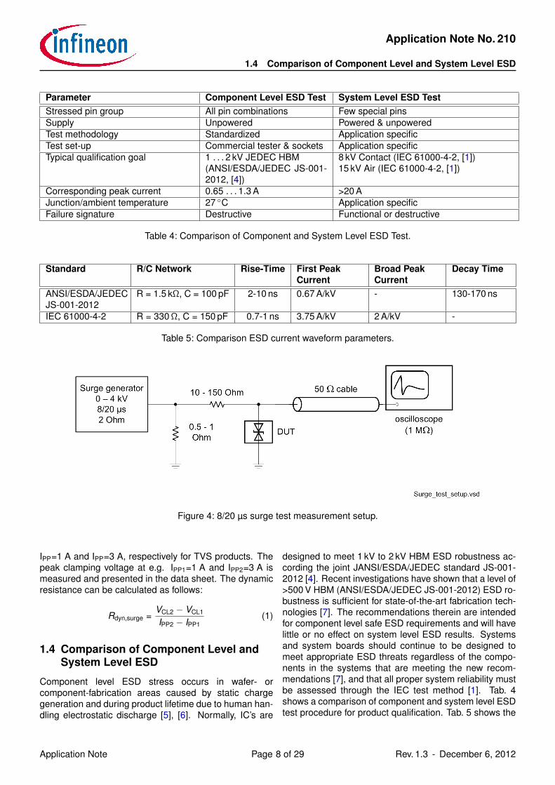
1.3.1 Surge Test Measurement Setup
Fig. 4 shows the measurement setup for the 8/20 µssurge test of TVS diodes. The amplitude of the pulsegenerator is adjusted for typical peak current (Fig. 3) of
1Depends on class of local power supply system.
Application Note Page 7 of 29 Rev. 1.3 - December 6, 2012
Application Note No. 210
1.4 Comparison of Component Level and System Level ESD
Parameter Component Level ESD Test System Level ESD TestStressed pin group All pin combinations Few special pinsSupply Unpowered Powered & unpoweredTest methodology Standardized Application specificTest set-up Commercial tester & sockets Application specificTypical qualification goal 1 . . . 2 kV JEDEC HBM
(ANSI/ESDA/JEDEC JS-001-2012, [4])
8 kV Contact (IEC 61000-4-2, [1])15 kV Air (IEC 61000-4-2, [1])
Corresponding peak current 0.65 . . . 1.3 A >20 AJunction/ambient temperature 27 C Application specificFailure signature Destructive Functional or destructive
Table 4: Comparison of Component and System Level ESD Test.
Standard R/C Network Rise-Time First PeakCurrent
Broad PeakCurrent
Decay Time
ANSI/ESDA/JEDECJS-001-2012
R = 1.5 kΩ, C = 100 pF 2-10 ns 0.67 A/kV - 130-170 ns
IEC 61000-4-2 R = 330Ω, C = 150 pF 0.7-1 ns 3.75 A/kV 2 A/kV -
Table 5: Comparison ESD current waveform parameters.
Figure 4: 8/20 µs surge test measurement setup.
IPP=1 A and IPP=3 A, respectively for TVS products. Thepeak clamping voltage at e.g. IPP1=1 A and IPP2=3 A ismeasured and presented in the data sheet. The dynamicresistance can be calculated as follows:
Rdyn,surge =VCL2 − VCL1
IPP2 − IPP1(1)
1.4 Comparison of Component Level andSystem Level ESD
Component level ESD stress occurs in wafer- orcomponent-fabrication areas caused by static chargegeneration and during product lifetime due to human han-dling electrostatic discharge [5], [6]. Normally, IC’s are
designed to meet 1 kV to 2 kV HBM ESD robustness ac-cording the joint JANSI/ESDA/JEDEC standard JS-001-2012 [4]. Recent investigations have shown that a level of>500 V HBM (ANSI/ESDA/JEDEC JS-001-2012) ESD ro-bustness is sufficient for state-of-the-art fabrication tech-nologies [7]. The recommendations therein are intendedfor component level safe ESD requirements and will havelittle or no effect on system level ESD results. Systemsand system boards should continue to be designed tomeet appropriate ESD threats regardless of the compo-nents in the systems that are meeting the new recom-mendations [7], and that all proper system reliability mustbe assessed through the IEC test method [1]. Tab. 4shows a comparison of component and system level ESDtest procedure for product qualification. Tab. 5 shows the
Application Note Page 8 of 29 Rev. 1.3 - December 6, 2012
Application Note No. 210
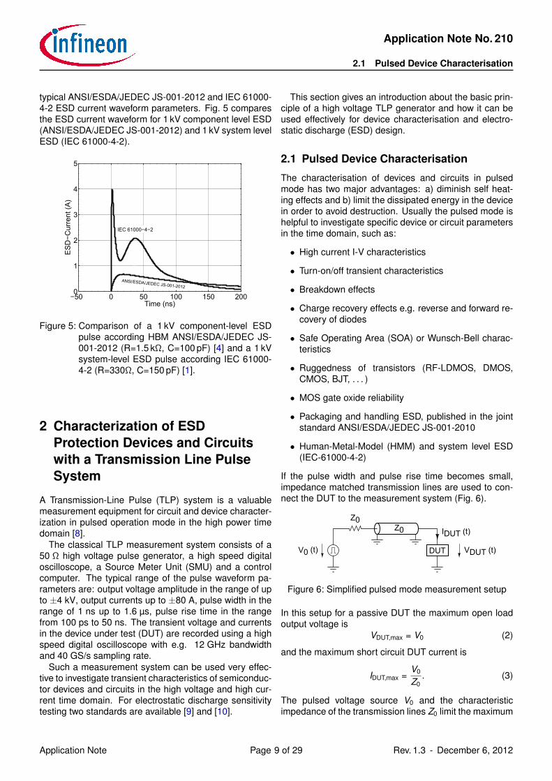
2.1 Pulsed Device Characterisation
typical ANSI/ESDA/JEDEC JS-001-2012 and IEC 61000-4-2 ESD current waveform parameters. Fig. 5 comparesthe ESD current waveform for 1 kV component level ESD(ANSI/ESDA/JEDEC JS-001-2012) and 1 kV system levelESD (IEC 61000-4-2).
−50 0 50 100 150 2000
1
2
3
4
5
IEC 61000−4−2
Time (ns)
ES
D−
Cur
rent
(A
)
ANSI/ESDA/JEDEC JS-001-2012
Figure 5: Comparison of a 1 kV component-level ESDpulse according HBM ANSI/ESDA/JEDEC JS-001-2012 (R=1.5 kΩ, C=100 pF) [4] and a 1 kVsystem-level ESD pulse according IEC 61000-4-2 (R=330Ω, C=150 pF) [1].
2 Characterization of ESDProtection Devices and Circuitswith a Transmission Line PulseSystem
A Transmission-Line Pulse (TLP) system is a valuablemeasurement equipment for circuit and device character-ization in pulsed operation mode in the high power timedomain [8].
The classical TLP measurement system consists of a50 Ω high voltage pulse generator, a high speed digitaloscilloscope, a Source Meter Unit (SMU) and a controlcomputer. The typical range of the pulse waveform pa-rameters are: output voltage amplitude in the range of upto ±4 kV, output currents up to ±80 A, pulse width in therange of 1 ns up to 1.6 µs, pulse rise time in the rangefrom 100 ps to 50 ns. The transient voltage and currentsin the device under test (DUT) are recorded using a highspeed digital oscilloscope with e.g. 12 GHz bandwidthand 40 GS/s sampling rate.
Such a measurement system can be used very effec-tive to investigate transient characteristics of semiconduc-tor devices and circuits in the high voltage and high cur-rent time domain. For electrostatic discharge sensitivitytesting two standards are available [9] and [10].
This section gives an introduction about the basic prin-ciple of a high voltage TLP generator and how it can beused effectively for device characterisation and electro-static discharge (ESD) design.
2.1 Pulsed Device Characterisation
The characterisation of devices and circuits in pulsedmode has two major advantages: a) diminish self heat-ing effects and b) limit the dissipated energy in the devicein order to avoid destruction. Usually the pulsed mode ishelpful to investigate specific device or circuit parametersin the time domain, such as:
• High current I-V characteristics
• Turn-on/off transient characteristics
• Breakdown effects
• Charge recovery effects e.g. reverse and forward re-covery of diodes
• Safe Operating Area (SOA) or Wunsch-Bell charac-teristics
• Ruggedness of transistors (RF-LDMOS, DMOS,CMOS, BJT, . . . )
• MOS gate oxide reliability
• Packaging and handling ESD, published in the jointstandard ANSI/ESDA/JEDEC JS-001-2010
• Human-Metal-Model (HMM) and system level ESD(IEC-61000-4-2)
If the pulse width and pulse rise time becomes small,impedance matched transmission lines are used to con-nect the DUT to the measurement system (Fig. 6).
Z0Z0
DUTV0 (t) VDUT (t)
IDUT (t)
Figure 6: Simplified pulsed mode measurement setup
In this setup for a passive DUT the maximum open loadoutput voltage is
VDUT,max = V0 (2)
and the maximum short circuit DUT current is
IDUT,max =V0
Z0. (3)
The pulsed voltage source V0 and the characteristicimpedance of the transmission lines Z0 limit the maximum
Application Note Page 9 of 29 Rev. 1.3 - December 6, 2012
Application Note No. 210
2.2 The Transmission Line Pulse Generator
DUT voltage and short circuit DUT current. To achievehigher level of VDUT and IDUT, V0 can be increased and Z0can be decreased.
Usually Z0 = 50Ω is widely used as a compromise be-tween low loss and power handling capability for coax-ial cables and measurement systems [11]. Example:in order to achieve 40 A short circuit DUT current in aZ0 = 50Ω system, a pulsed voltage source of 2 kV is re-quired.
So far no commercial pulse generators based on solid-state devices or vacuum tubes are available to handlesuch high voltage with excellent pulse waveform qual-ity with a dynamic range from below 1 V up to severalkilo volts amplitude. The concept of using high voltagecharged transmission lines to generate rectangular pulsewaveforms with high quality is well known for a very longtime, which has been described in [12] or even much ear-lier. This leads us to the classical transmission line pulsegenerator.
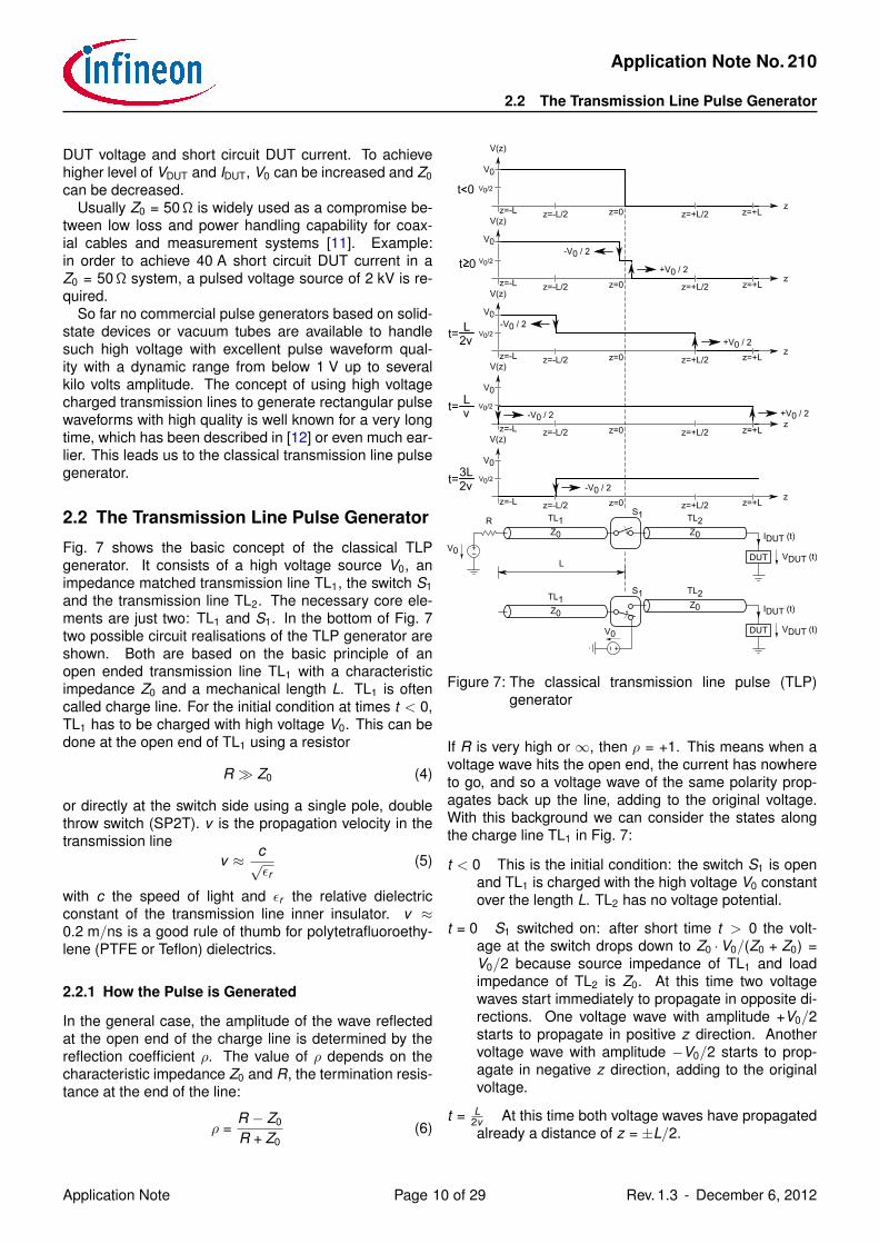
2.2 The Transmission Line Pulse Generator
Fig. 7 shows the basic concept of the classical TLPgenerator. It consists of a high voltage source V0, animpedance matched transmission line TL1, the switch S1and the transmission line TL2. The necessary core ele-ments are just two: TL1 and S1. In the bottom of Fig. 7two possible circuit realisations of the TLP generator areshown. Both are based on the basic principle of anopen ended transmission line TL1 with a characteristicimpedance Z0 and a mechanical length L. TL1 is oftencalled charge line. For the initial condition at times t < 0,TL1 has to be charged with high voltage V0. This can bedone at the open end of TL1 using a resistor
R Z0 (4)
or directly at the switch side using a single pole, doublethrow switch (SP2T). v is the propagation velocity in thetransmission line
v ≈ c√εr
(5)
with c the speed of light and εr the relative dielectricconstant of the transmission line inner insulator. v ≈0.2 m/ns is a good rule of thumb for polytetrafluoroethy-lene (PTFE or Teflon) dielectrics.
2.2.1 How the Pulse is Generated
In the general case, the amplitude of the wave reflectedat the open end of the charge line is determined by thereflection coefficient ρ. The value of ρ depends on thecharacteristic impedance Z0 and R, the termination resis-tance at the end of the line:
ρ =R − Z0
R + Z0(6)
Z0
DUTV0
VDUT (t)
IDUT (t)+−
R TL1S1
Z0
V0
TL1S1
+−
L
z
V(z)
V0
Z0
TL2
DUT VDUT (t)
IDUT (t)Z0
z
V(z)
V0
z
V(z)
V0
z
V0
+V0 / 2
-V0 / 2
TL2
-V0 / 2
+V0 / 2
+V0 / 2-V0 / 2
z
V(z)
V0
-V0 / 2
V(z)
z=0
z=0
z=0
z=0
z=0
V0/2
V0/2
V0/2
V0/2
V0/2
z=-L
z=-L
z=-L
z=-L
z=+L
z=+L
z=+L
z=+L
z=+L
z=+L/2z=-L/2
z=-L z=+L/2z=-L/2
z=+L/2z=-L/2
z=+L/2z=-L/2
z=+L/2z=-L/2
Figure 7: The classical transmission line pulse (TLP)generator
If R is very high or ∞, then ρ = +1. This means when avoltage wave hits the open end, the current has nowhereto go, and so a voltage wave of the same polarity prop-agates back up the line, adding to the original voltage.With this background we can consider the states alongthe charge line TL1 in Fig. 7:
t < 0 This is the initial condition: the switch S1 is openand TL1 is charged with the high voltage V0 constantover the length L. TL2 has no voltage potential.
t = 0 S1 switched on: after short time t > 0 the volt-age at the switch drops down to Z0 ·V0/(Z0 + Z0) =V0/2 because source impedance of TL1 and loadimpedance of TL2 is Z0. At this time two voltagewaves start immediately to propagate in opposite di-rections. One voltage wave with amplitude +V0/2starts to propagate in positive z direction. Anothervoltage wave with amplitude −V0/2 starts to prop-agate in negative z direction, adding to the originalvoltage.
t = L2v At this time both voltage waves have propagatedalready a distance of z = ±L/2.
Application Note Page 10 of 29 Rev. 1.3 - December 6, 2012
Application Note No. 210
2.3 The TLP Measurement System
500 mV
500 ps
Figure 8: TLP waveform measurement result at 40 GS/s
t = Lv The voltage wave along negative z direction withamplitude −V0/2 hits the open end of TL1. A voltagewave with same polarity propagates back up the lineand adds to the original voltage −V0/2 + V0/2 = 0which leads to cancellation.
t = 3L2v The cancellation voltage wave propagates backup the line and has reached z = −L/2. At the sametime the other voltage wave with +V0/2 amplitudehas reached the location z = 3L/2 (not shown inFig. 7).
This consideration leads to the conclusion that a rectan-gular pulse waveform is propagating along the transmis-sion lines. On the transmission line a mechanical dis-tance of 2L is travelled by the waveform and the pulsewidth in the time domain is
tp =2Lv≈√εr ·
2Lc
(7)
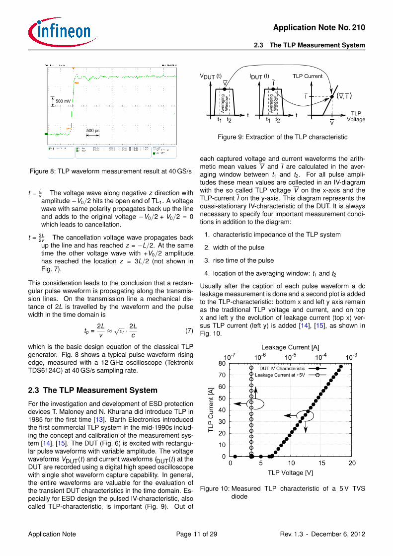
which is the basic design equation of the classical TLPgenerator. Fig. 8 shows a typical pulse waveform risingedge, measured with a 12 GHz oscilloscope (TektronixTDS6124C) at 40 GS/s sampling rate.
2.3 The TLP Measurement System
For the investigation and development of ESD protectiondevices T. Maloney and N. Khurana did introduce TLP in1985 for the first time [13]. Barth Electronics introducedthe first commercial TLP system in the mid-1990s includ-ing the concept and calibration of the measurement sys-tem [14], [15]. The DUT (Fig. 6) is excited with rectangu-lar pulse waveforms with variable amplitude. The voltagewaveforms VDUT(t) and current waveforms IDUT(t) at theDUT are recorded using a digital high speed oscilloscopewith single shot waveform capture capability. In general,the entire waveforms are valuable for the evaluation ofthe transient DUT characteristics in the time domain. Es-pecially for ESD design the pulsed IV-characteristic, alsocalled TLP-characteristic, is important (Fig. 9). Out of
Ave
ragi
ngW
indo
w
VDUT (t)
t
V
Ave
ragi
ngW
indo
w
IDUT (t)
t
I
V
TLP Current
TLPVoltage
I V, I( )
t1 t2 t1 t2
Figure 9: Extraction of the TLP characteristic
each captured voltage and current waveforms the arith-metic mean values V and I are calculated in the aver-aging window between t1 and t2. For all pulse ampli-tudes these mean values are collected in an IV-diagramwith the so called TLP voltage V on the x-axis and theTLP-current I on the y-axis. This diagram represents thequasi-stationary IV-characteristic of the DUT. It is alwaysnecessary to specify four important measurement condi-tions in addition to the diagram:
1. characteristic impedance of the TLP system
2. width of the pulse
3. rise time of the pulse
4. location of the averaging window: t1 and t2
Usually after the caption of each pulse waveform a dcleakage measurement is done and a second plot is addedto the TLP-characteristic: bottom x and left y axis remainas the traditional TLP voltage and current, and on topx and left y the evolution of leakage current (top x) ver-sus TLP current (left y) is added [14], [15], as shown inFig. 10.
0
10
20
30
40
50
60
70
80
0 5 10 15 20
10-7 10-6 10-5 10-4 10-3
TLP
Cur
rent
[A]
TLP Voltage [V]
Leakage Current [A]
DUT IV CharacteristicLeakage Current at +5V
Figure 10: Measured TLP characteristic of a 5 V TVSdiode
Application Note Page 11 of 29 Rev. 1.3 - December 6, 2012
Application Note No. 210
2.3 The TLP Measurement System
2.3.1 Discrete Voltage and Current Sensors
Fig. 11 shows a pulsed mode measurement setup withdiscrete sensors for current and voltage. The sensorsshould be located as close as possible to the DUT.
DUTV0 (t) VDUT (t)
IDUT (t)50 Ω
50 Ω
TLP Generator
Oscilloscope
50 Ω
50 Ω
IDUT (t)
VDUT (t)
Hig
h Im
peda
nce
Pro
be
Current Sensor
Figure 11: Pulsed mode measurement setup with dis-crete sensors
50 Ω
4.95 kΩ
Voltage SensorOutput
Pulse Input
(a) High impedance probe
50 Ω
PulseInput
50 Ω
50 Ω
PulseOutput
Current SensorOutput
(b) Current sensor
Figure 12: Discrete voltage and current sensors
Fig. 12 show practical realisations for discrete voltageand current probes. Voltage probes can be realised eas-ier for higher bandwidth than current probes. The highimpedance V-probe shown in Fig. 12(a) has an inputimpedance of 5 kΩ and a sensitivity (or voltage divisionratio) of 50/(4950 + 50) = 0.01 V/V. The voltage sensoroutput must be terminated with 50 Ω. GGB [16] offersprobe tips with such integrated resistors (Model 10) forwafer-level testing up to 11 GHz.
Discrete I-probes for pulse waveforms are often basedon transformers, as shown in Fig. 12(b). The TektronixCT-1 and CT-2 current sensors [17] have become an in-dustry standard for TLP applications up to 100 A, de-pending on the pulse width tp.
Tab. 6 summarises the typical specifications of the Tek-tronix CT-1 and CT-2 current sensors. The maximum cur-rent depends on the pulse width and is limited by the L/Rtime constant and the amp x second rating. If the product(current x pulse width) exceeds the maximum rating, thecore saturates and the output drops to zero.
Sensor Sensitivity Bandwidth Rise Time A x µs[V/A] [GHz] [ns] Rating
CT-1 5 1 < 0.35 1CT-2 1 0.2 < 0.5 50
Table 6: Comparison of current sensor parameters [17]
DUTV0 (t) VDUT (t)
IDUT (t)50 Ω
50 Ω
TLP Generator
Oscilloscope
50 Ω
PickoffTee
50 Ω
DelayLine
LD
VI(t), VR(t)
Figure 14: Simplified VF-TLP measurement setup
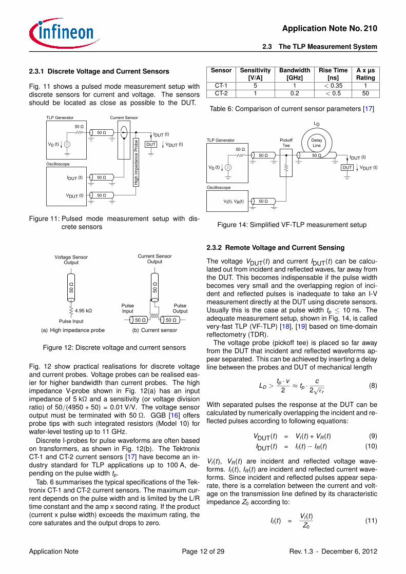
2.3.2 Remote Voltage and Current Sensing
The voltage VDUT(t) and current IDUT(t) can be calcu-lated out from incident and reflected waves, far away fromthe DUT. This becomes indispensable if the pulse widthbecomes very small and the overlapping region of inci-dent and reflected pulses is inadequate to take an I-Vmeasurement directly at the DUT using discrete sensors.Usually this is the case at pulse width tp ≤ 10 ns. Theadequate measurement setup, shown in Fig. 14, is calledvery-fast TLP (VF-TLP) [18], [19] based on time-domainreflectometry (TDR).
The voltage probe (pickoff tee) is placed so far awayfrom the DUT that incident and reflected waveforms ap-pear separated. This can be achieved by inserting a delayline between the probes and DUT of mechanical length
LD >tp · v
2≈ tp ·
c2√εr
(8)
With separated pulses the response at the DUT can becalculated by numerically overlapping the incident and re-flected pulses according to following equations:
VDUT(t) = VI(t) + VR(t) (9)IDUT(t) = II(t)− IR(t) (10)
VI(t), VR(t) are incident and reflected voltage wave-forms. II(t), IR(t) are incident and reflected current wave-forms. Since incident and reflected pulses appear sepa-rate, there is a correlation between the current and volt-age on the transmission line defined by its characteristicimpedance Z0 according to:
II(t) =VI(t)Z0
(11)
Application Note Page 12 of 29 Rev. 1.3 - December 6, 2012
Application Note No. 210
2.4 Measurement Techniques
LEAKAGETEST
DUT Leakage Test
Switch Control
50 Ω Pulse Output
LeakageDUT
Pulse
GPIB
GPIB
GPIB
DUT Pulse Force
DUT Pulse Sense
DUT
5 kΩ PicoprobeModel 10
PAD PAD
50 Ω PicoprobeModel 10
5 kΩ50 Ω
50 Ω
CURRENT SENSOR
50 Ω50 Ω
A1
Pulse Sense
50 Ω
TLPGENERATOR
SWITCHDIGITAL
OSCILLOSCOPE
PC
+ S
yste
m C
on
tro
l So
ftw
are
SMU
Current
VDUT (t)
IDUT (t)
L < 2 inch
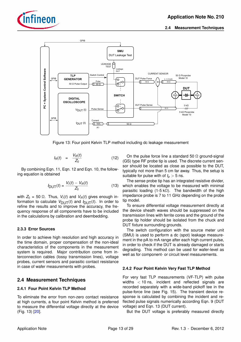
Figure 13: Four point Kelvin TLP method including dc leakage measurement
IR(t) =VR(t)
Z0(12)
By combining Eqn. 11, Eqn. 12 and Eqn. 10, the follow-ing equation is obtained
IDUT(t) =VI(t)− VR(t)
Z0(13)
with Z0 = 50 Ω. Thus, VI(t) and VR(t) gives enough in-formation to calculate VDUT(t) and IDUT(t). In order torefine the results and to improve the accuracy, the fre-quency response of all components have to be includedin the calculations by calibration and deembedding.
2.3.3 Error Sources
In order to achieve high resolution and high accuracy inthe time domain, proper compensation of the non-idealcharacteristics of the components in the measurementsystem is required. Major contribution come from in-terconnection cables (lossy transmission lines), voltageprobes, current sensors and parasitic contact resistancein case of wafer measurements with probes.
2.4 Measurement Techniques
2.4.1 Four Point Kelvin TLP Method
To eliminate the error from non-zero contact resistanceat high currents, a four point Kelvin method is preferredto measure the differential voltage directly at the device(Fig. 13) [20].
On the pulse force line a standard 50 Ω ground-signal(GS) type RF probe tip is used. The discrete current sen-sor should be located as close as possible to the DUT,typically not more than 5 cm far away. Thus, the setup issuitable for pulse with of tp > 5 ns.
The sense probe tip has an integrated resistive divider,which enables the voltage to be measured with minimalparasitic loading (1-5 kΩ). The bandwidth of the highimpedance probe is 7 to 11 GHz depending on the probetip model.
To ensure differential voltage measurement directly atthe device sheath waves should be suppressed on thetransmission lines with ferrite cores and the ground of theprobe tip holder should be isolated from the chuck andDUT fixture surrounding grounds.
The switch configuration with the source meter unit(SMU) is used to perform a dc (spot) leakage measure-ment in the pA to mA range after each high current pulse,in order to check if the DUT is already damaged or startsdegrading. This method can be used for wafer-level aswell as for component- or circuit level measurements.
2.4.2 Four Point Kelvin Very Fast TLP Method
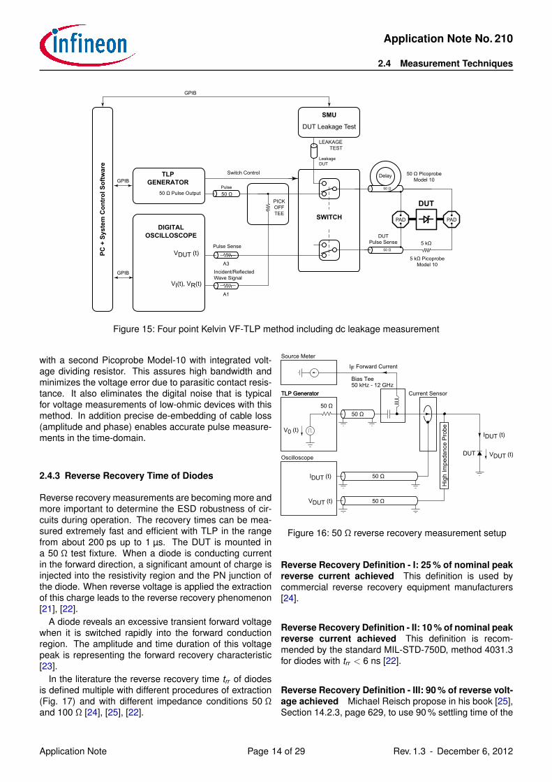
For very fast TLP measurements (VF-TLP) with pulsewidths < 10 ns, incident and reflected signals arerecorded separately with a wide-band pickoff tee in thepulse-force line (see Fig. 15). The transient device re-sponse is calculated by combining the incident and re-flected pulse signals numerically according Eqn. 9 (DUTvoltage) and Eqn. 13 (DUT current).
But the DUT voltage is preferably measured directly
Application Note Page 13 of 29 Rev. 1.3 - December 6, 2012
Application Note No. 210
2.4 Measurement Techniques
VDUT (t)
LEAKAGETEST
DUT Leakage Test
Switch Control
50 Ω Pulse Output
LeakageDUT
Pulse
GPIB
GPIB
GPIB
DUTPulse Sense
DUT
5 kΩ PicoprobeModel 10
PAD PAD
50 Ω PicoprobeModel 10
5 kΩ50 Ω
50 Ω
A1
Pulse Sense
50 Ω
Delay
PICKOFFTEE
A3
Incident/ReflectedWave Signal
PC
+ S
yste
m C
on
tro
l So
ftw
are
TLPGENERATOR
DIGITALOSCILLOSCOPE
SWITCH
SMU
VI(t), VR(t)
Figure 15: Four point Kelvin VF-TLP method including dc leakage measurement
with a second Picoprobe Model-10 with integrated volt-age dividing resistor. This assures high bandwidth andminimizes the voltage error due to parasitic contact resis-tance. It also eliminates the digital noise that is typicalfor voltage measurements of low-ohmic devices with thismethod. In addition precise de-embedding of cable loss(amplitude and phase) enables accurate pulse measure-ments in the time-domain.
2.4.3 Reverse Recovery Time of Diodes
Reverse recovery measurements are becoming more andmore important to determine the ESD robustness of cir-cuits during operation. The recovery times can be mea-sured extremely fast and efficient with TLP in the rangefrom about 200 ps up to 1 µs. The DUT is mounted ina 50 Ω test fixture. When a diode is conducting currentin the forward direction, a significant amount of charge isinjected into the resistivity region and the PN junction ofthe diode. When reverse voltage is applied the extractionof this charge leads to the reverse recovery phenomenon[21], [22].
A diode reveals an excessive transient forward voltagewhen it is switched rapidly into the forward conductionregion. The amplitude and time duration of this voltagepeak is representing the forward recovery characteristic[23].
In the literature the reverse recovery time trr of diodesis defined multiple with different procedures of extraction(Fig. 17) and with different impedance conditions 50 Ωand 100 Ω [24], [25], [22].
V0 (t)
50 Ω
TLP Generator
Oscilloscope
50 Ω
50 Ω
IDUT (t)
VDUT (t)
Hig
h Im
peda
nce
Pro
be
Current Sensor
VDUT (t)
IDUT (t)
DUT
50 Ω
TLP Generator
Source Meter
Bias Tee50 kHz - 12 GHz
IF Forward Current
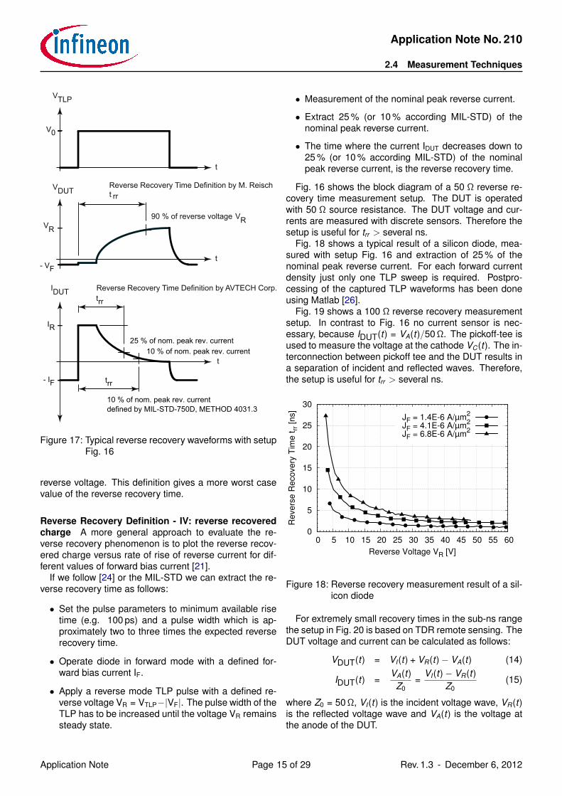
Figure 16: 50 Ω reverse recovery measurement setup
Reverse Recovery Definition - I: 25 % of nominal peakreverse current achieved This definition is used bycommercial reverse recovery equipment manufacturers[24].
Reverse Recovery Definition - II: 10 % of nominal peakreverse current achieved This definition is recom-mended by the standard MIL-STD-750D, method 4031.3for diodes with trr < 6 ns [22].
Reverse Recovery Definition - III: 90 % of reverse volt-age achieved Michael Reisch propose in his book [25],Section 14.2.3, page 629, to use 90 % settling time of the
Application Note Page 14 of 29 Rev. 1.3 - December 6, 2012
Application Note No. 210
2.4 Measurement Techniques
t
VTLP
IDUT
t
t
VDUT
VR
Reverse Recovery Time Definition by AVTECH Corp.
90 % of reverse voltage VR
tReverse Recovery Time Definition by M. Reisch
rr
IR
V0
25 % of nom. peak rev. current
- IF
- VF
trr
10 % of nom. peak rev. currentdefined by MIL-STD-750D, METHOD 4031.3
trr
10 % of nom. peak rev. current
Figure 17: Typical reverse recovery waveforms with setupFig. 16
reverse voltage. This definition gives a more worst casevalue of the reverse recovery time.
Reverse Recovery Definition - IV: reverse recoveredcharge A more general approach to evaluate the re-verse recovery phenomenon is to plot the reverse recov-ered charge versus rate of rise of reverse current for dif-ferent values of forward bias current [21].
If we follow [24] or the MIL-STD we can extract the re-verse recovery time as follows:
• Set the pulse parameters to minimum available risetime (e.g. 100 ps) and a pulse width which is ap-proximately two to three times the expected reverserecovery time.
• Operate diode in forward mode with a defined for-ward bias current IF.
• Apply a reverse mode TLP pulse with a defined re-verse voltage VR = VTLP−|VF|. The pulse width of theTLP has to be increased until the voltage VR remainssteady state.
• Measurement of the nominal peak reverse current.
• Extract 25 % (or 10 % according MIL-STD) of thenominal peak reverse current.
• The time where the current IDUT decreases down to25 % (or 10 % according MIL-STD) of the nominalpeak reverse current, is the reverse recovery time.
Fig. 16 shows the block diagram of a 50 Ω reverse re-covery time measurement setup. The DUT is operatedwith 50 Ω source resistance. The DUT voltage and cur-rents are measured with discrete sensors. Therefore thesetup is useful for trr > several ns.
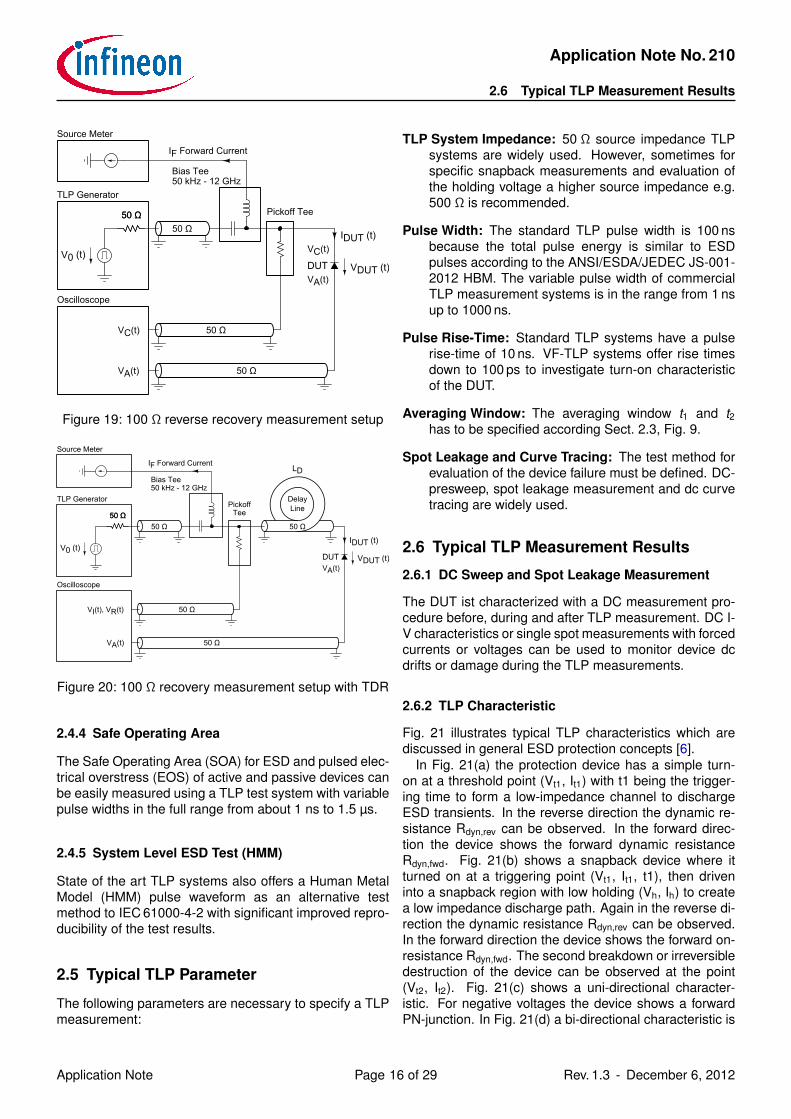
Fig. 18 shows a typical result of a silicon diode, mea-sured with setup Fig. 16 and extraction of 25 % of thenominal peak reverse current. For each forward currentdensity just only one TLP sweep is required. Postpro-cessing of the captured TLP waveforms has been doneusing Matlab [26].
Fig. 19 shows a 100 Ω reverse recovery measurementsetup. In contrast to Fig. 16 no current sensor is nec-essary, because IDUT(t) = VA(t)/50Ω. The pickoff-tee isused to measure the voltage at the cathode VC(t). The in-terconnection between pickoff tee and the DUT results ina separation of incident and reflected waves. Therefore,the setup is useful for trr > several ns.
0
5
10
15
20
25
30
0 5 10 15 20 25 30 35 40 45 50 55 60
Re
ve
rse
Re
co
ve
ry T
ime
trr [
ns]
Reverse Voltage VR [V]
JF = 1.4E-6 A/µm2
JF = 4.1E-6 A/µm2
JF = 6.8E-6 A/µm2
Figure 18: Reverse recovery measurement result of a sil-icon diode
For extremely small recovery times in the sub-ns rangethe setup in Fig. 20 is based on TDR remote sensing. TheDUT voltage and current can be calculated as follows:
VDUT(t) = VI(t) + VR(t)− VA(t) (14)
IDUT(t) =VA(t)
Z0=
VI(t)− VR(t)Z0
(15)
where Z0 = 50Ω, VI(t) is the incident voltage wave, VR(t)is the reflected voltage wave and VA(t) is the voltage atthe anode of the DUT.
Application Note Page 15 of 29 Rev. 1.3 - December 6, 2012
Application Note No. 210
2.6 Typical TLP Measurement Results
V0 (t)VDUT (t)
IDUT (t)50 Ω
50 Ω
TLP Generator
Oscilloscope
50 Ω
50 Ω
Source Meter
DUT
Bias Tee50 kHz - 12 GHz
Pickoff Tee
IF Forward Current
VC(t)
VA(t)
VC(t)
VA(t)
50 Ω
Figure 19: 100 Ω reverse recovery measurement setup
V0 (t)VDUT (t)
IDUT (t)
50 Ω
50 Ω
TLP Generator
Oscilloscope
50 Ω
50 Ω
Source Meter
DUT
Bias Tee50 kHz - 12 GHz
PickoffTee
IF Forward Current
VA(t)
VA(t)
50 Ω
50 Ω
DelayLine
LD
VI(t), VR(t)
Figure 20: 100 Ω recovery measurement setup with TDR
2.4.4 Safe Operating Area
The Safe Operating Area (SOA) for ESD and pulsed elec-trical overstress (EOS) of active and passive devices canbe easily measured using a TLP test system with variablepulse widths in the full range from about 1 ns to 1.5 µs.
2.4.5 System Level ESD Test (HMM)
State of the art TLP systems also offers a Human MetalModel (HMM) pulse waveform as an alternative testmethod to IEC 61000-4-2 with significant improved repro-ducibility of the test results.
2.5 Typical TLP Parameter
The following parameters are necessary to specify a TLPmeasurement:
TLP System Impedance: 50 Ω source impedance TLPsystems are widely used. However, sometimes forspecific snapback measurements and evaluation ofthe holding voltage a higher source impedance e.g.500 Ω is recommended.
Pulse Width: The standard TLP pulse width is 100 nsbecause the total pulse energy is similar to ESDpulses according to the ANSI/ESDA/JEDEC JS-001-2012 HBM. The variable pulse width of commercialTLP measurement systems is in the range from 1 nsup to 1000 ns.
Pulse Rise-Time: Standard TLP systems have a pulserise-time of 10 ns. VF-TLP systems offer rise timesdown to 100 ps to investigate turn-on characteristicof the DUT.
Averaging Window: The averaging window t1 and t2has to be specified according Sect. 2.3, Fig. 9.
Spot Leakage and Curve Tracing: The test method forevaluation of the device failure must be defined. DC-presweep, spot leakage measurement and dc curvetracing are widely used.
2.6 Typical TLP Measurement Results
2.6.1 DC Sweep and Spot Leakage Measurement
The DUT ist characterized with a DC measurement pro-cedure before, during and after TLP measurement. DC I-V characteristics or single spot measurements with forcedcurrents or voltages can be used to monitor device dcdrifts or damage during the TLP measurements.
2.6.2 TLP Characteristic
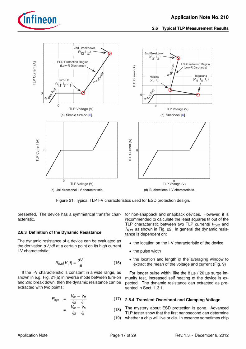
Fig. 21 illustrates typical TLP characteristics which arediscussed in general ESD protection concepts [6].
In Fig. 21(a) the protection device has a simple turn-on at a threshold point (Vt1, It1) with t1 being the trigger-ing time to form a low-impedance channel to dischargeESD transients. In the reverse direction the dynamic re-sistance Rdyn,rev can be observed. In the forward direc-tion the device shows the forward dynamic resistanceRdyn,fwd. Fig. 21(b) shows a snapback device where itturned on at a triggering point (Vt1, It1, t1), then driveninto a snapback region with low holding (Vh, Ih) to createa low impedance discharge path. Again in the reverse di-rection the dynamic resistance Rdyn,rev can be observed.In the forward direction the device shows the forward on-resistance Rdyn,fwd. The second breakdown or irreversibledestruction of the device can be observed at the point(Vt2, It2). Fig. 21(c) shows a uni-directional character-istic. For negative voltages the device shows a forwardPN-junction. In Fig. 21(d) a bi-directional characteristic is
Application Note Page 16 of 29 Rev. 1.3 - December 6, 2012
Application Note No. 210
2.6 Typical TLP Measurement Results
0
0
TLP Voltage (V)
TLP
Cur
rent
(A) ESD Protection Region
(Low-R Discharge)
Turn-On(Vt1, It1, t1)
R dyn,
fwd
dy
n,re
v
R
, I2nd Breakdown
(Vt2 t2),I
(a) Simple turn-on [6].
0
0
TLP Voltage (V)
TLP
Cur
rent
(A) ESD Protection Region
(Low-R Discharge)
Triggering(Vt1, It1, t1)
R dyn ,
rev
R dyn,
fwd
Holding(Vh, Ih)
2nd Breakdown(Vt2, It2)
(b) Snapback [6].
0
0
TLP Voltage (V)
TLP
Cur
rent
(A)
(c) Uni-directional I-V characteristic.
0
0
TLP Voltage (V)
TLP
Cur
rent
(A)
(d) Bi-directional I-V characteristic.
Figure 21: Typical TLP I-V characteristics used for ESD protection design.
presented. The device has a symmetrical transfer char-acteristic.
2.6.3 Definition of the Dynamic Resistance
The dynamic resistance of a device can be evaluated asthe derivation dV/dI at a certain point on its high currentI-V characteristic:
Rdyn(V , I) =dVdI
(16)
If the I-V characteristic is constant in a wide range, asshown in e.g. Fig. 21(a) in reverse mode between turn-onand 2nd break down, then the dynamic resistance can beextracted with two points:
Rdyn =Vt2 − Vt1
It2 − It1(17)
=Vt2 − Vh
It2 − Ih(18)
(19)
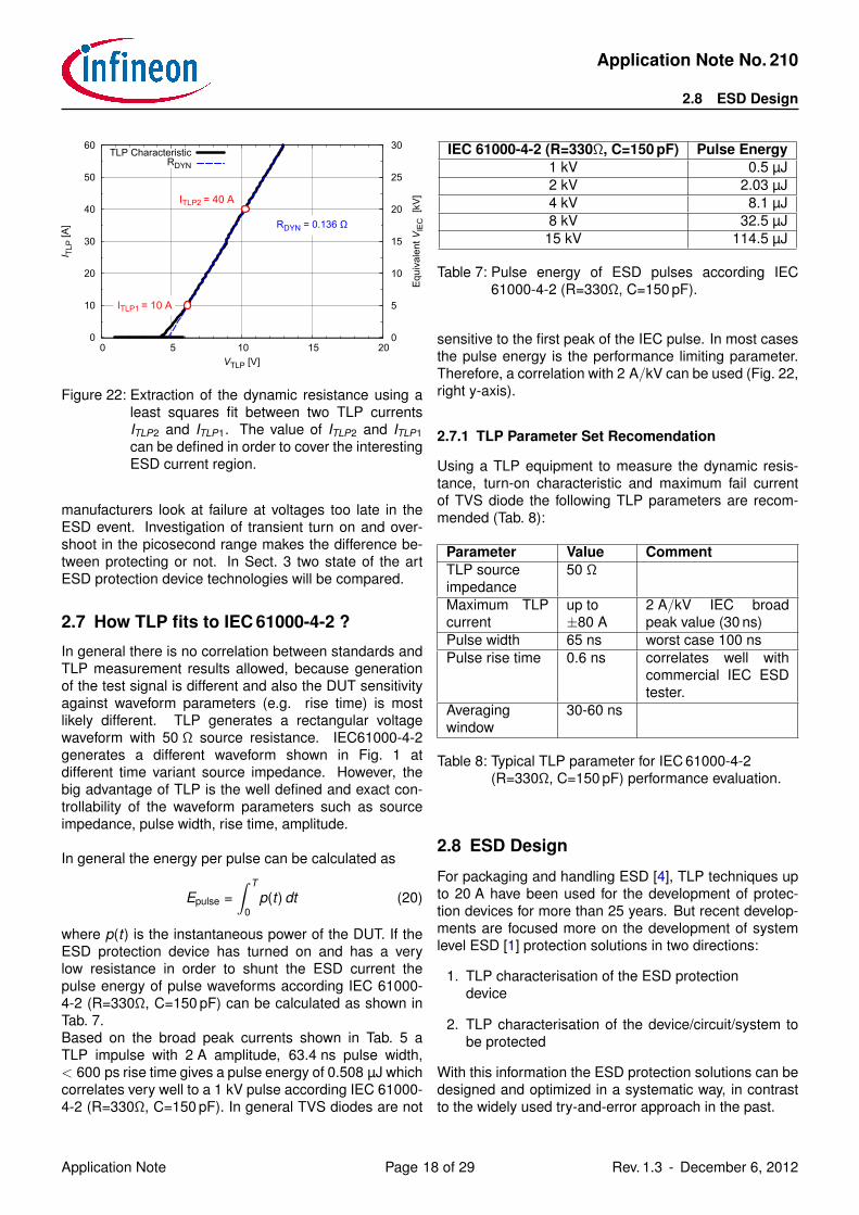
for non-snapback and snapback devices. However, it isrecommended to calculate the least squares fit out of theTLP characteristic between two TLP currents ITLP2 andITLP1 as shown in Fig. 22. In general the dynamic resis-tance is dependent on:
• the location on the I-V characteristic of the device
• the pulse width
• the location and length of the averaging window toextract the mean of the voltage and current (Fig. 9)
For longer pulse width, like the 8 µs / 20 µs surge im-munity test, increased self heating of the device is ex-pected. The dynamic resistance can extracted as pre-sented in Sect. 1.3.1.
2.6.4 Transient Overshoot and Clamping Voltage
The mystery about ESD protection is gone. AdvancedTLP tester show that the first nanosecond can determinewhether a chip will live or die. In essence sometimes chip
Application Note Page 17 of 29 Rev. 1.3 - December 6, 2012
Application Note No. 210
2.8 ESD Design
0
10
20
30
40
50
60
0 5 10 15 200
5
10
15
20
25
30
I TLP
[A]
Equ
ival
ent V
IEC
[kV
]
VTLP [V]
RDYN
RDYN = 0.136 Ω
ITLP2 = 40 A
ITLP1 = 10 A
TLP Characteristic
Figure 22: Extraction of the dynamic resistance using aleast squares fit between two TLP currentsITLP2 and ITLP1. The value of ITLP2 and ITLP1can be defined in order to cover the interestingESD current region.
manufacturers look at failure at voltages too late in theESD event. Investigation of transient turn on and over-shoot in the picosecond range makes the difference be-tween protecting or not. In Sect. 3 two state of the artESD protection device technologies will be compared.
2.7 How TLP fits to IEC 61000-4-2 ?
In general there is no correlation between standards andTLP measurement results allowed, because generationof the test signal is different and also the DUT sensitivityagainst waveform parameters (e.g. rise time) is mostlikely different. TLP generates a rectangular voltagewaveform with 50 Ω source resistance. IEC61000-4-2generates a different waveform shown in Fig. 1 atdifferent time variant source impedance. However, thebig advantage of TLP is the well defined and exact con-trollability of the waveform parameters such as sourceimpedance, pulse width, rise time, amplitude.
In general the energy per pulse can be calculated as
Epulse =∫ T
0p(t) dt (20)
where p(t) is the instantaneous power of the DUT. If theESD protection device has turned on and has a verylow resistance in order to shunt the ESD current thepulse energy of pulse waveforms according IEC 61000-4-2 (R=330Ω, C=150 pF) can be calculated as shown inTab. 7.Based on the broad peak currents shown in Tab. 5 aTLP impulse with 2 A amplitude, 63.4 ns pulse width,< 600 ps rise time gives a pulse energy of 0.508 µJ whichcorrelates very well to a 1 kV pulse according IEC 61000-4-2 (R=330Ω, C=150 pF). In general TVS diodes are not
IEC 61000-4-2 (R=330Ω, C=150 pF) Pulse Energy1 kV 0.5 µJ2 kV 2.03 µJ4 kV 8.1 µJ8 kV 32.5 µJ
15 kV 114.5 µJ
Table 7: Pulse energy of ESD pulses according IEC61000-4-2 (R=330Ω, C=150 pF).
sensitive to the first peak of the IEC pulse. In most casesthe pulse energy is the performance limiting parameter.Therefore, a correlation with 2 A/kV can be used (Fig. 22,right y-axis).
2.7.1 TLP Parameter Set Recomendation
Using a TLP equipment to measure the dynamic resis-tance, turn-on characteristic and maximum fail currentof TVS diode the following TLP parameters are recom-mended (Tab. 8):
Parameter Value CommentTLP sourceimpedance
50 Ω
Maximum TLPcurrent
up to±80 A
2 A/kV IEC broadpeak value (30 ns)
Pulse width 65 ns worst case 100 nsPulse rise time 0.6 ns correlates well with
commercial IEC ESDtester.
Averagingwindow
30-60 ns
Table 8: Typical TLP parameter for IEC 61000-4-2(R=330Ω, C=150 pF) performance evaluation.
2.8 ESD Design
For packaging and handling ESD [4], TLP techniques upto 20 A have been used for the development of protec-tion devices for more than 25 years. But recent develop-ments are focused more on the development of systemlevel ESD [1] protection solutions in two directions:
1. TLP characterisation of the ESD protectiondevice
2. TLP characterisation of the device/circuit/system tobe protected
With this information the ESD protection solutions can bedesigned and optimized in a systematic way, in contrastto the widely used try-and-error approach in the past.
Application Note Page 18 of 29 Rev. 1.3 - December 6, 2012
Application Note No. 210
2.8 ESD Design
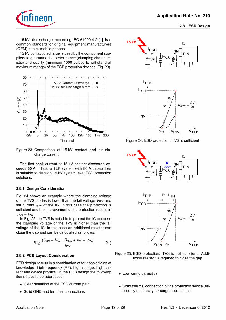
15 kV air discharge, according IEC-61000-4-2 [1], is acommon standard for original equipment manufacturers(OEM) of e.g. mobile phones.
15 kV contact discharge is used by the component sup-pliers to guarantee the performance (clamping character-istic) and quality (minimum 1000 pulses to withstand atmaximum ratings) of the ESD protection devices (Fig. 23).
0
10
20
30
40
50
60
70
80
-25 0 25 50 75 100 125 150 175 200
Cu
rre
nt
[A]
Time [ns]
15 kV Contact Discharge 15 kV Air Discharge 8 mm
Figure 23: Comparison of 15 kV contact and air dis-charge current.
The first peak current at 15 kV contact discharge ex-ceeds 60 A. Thus, a TLP system with 80 A capabilitiesis suitable to develop 15 kV system level ESD protectionsolutions.
2.8.1 Design Consideration
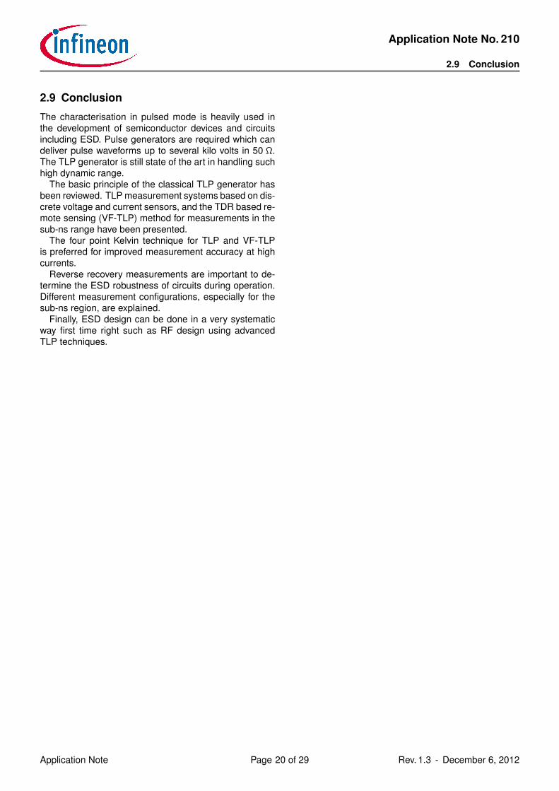
Fig. 24 shows an example where the clamping voltageof the TVS diodes is lower than the fail voltage VPIN andfail current IPIN of the IC. In this case the protection issufficient and the improvement of the protection results inIESD − IPIN .
In Fig. 25 the TVS is not able to protect the IC becausethe clamping voltage of the TVS is higher than the failvoltage of the IC. In this case an additional resistor canclose the gap and can be calculated as follows:
R ≥ (IESD − IPIN ) ·RDYN + Vt1 − VPIN
IPIN(21)
2.8.2 PCB Layout Consideration
ESD design results in a combination of four basic fields ofknowledge: high frequency (RF), high voltage, high cur-rent and device physics. In the PCB design the followingitems have to be addressed:
• Clear definition of the ESD current path
• Solid GND and terminal connections
PIN
15 kV IC
RDYNΔVΔIΔI
ΔV
IESD
IPIN
Vt1 VPIN VTLP
ITLP
IESD
VTVS
IPIN
ITVS
VPIN
Figure 24: ESD protection: TVS is sufficient
PINIESD
VTVS
15 kV IC
IPIN
ITVS
RDYNΔVΔIΔI
ΔV
IESD
IPIN
Vt1VPIN VTLP
ITLP R . IPIN
VP
IN
R
Figure 25: ESD protection: TVS is not sufficient. Addi-tional resistor is required to close the gap.
• Low wiring parasitics
• Solid thermal connection of the protection device (es-pecially necessary for surge applications)
Application Note Page 19 of 29 Rev. 1.3 - December 6, 2012
Application Note No. 210
2.9 Conclusion
2.9 Conclusion
The characterisation in pulsed mode is heavily used inthe development of semiconductor devices and circuitsincluding ESD. Pulse generators are required which candeliver pulse waveforms up to several kilo volts in 50 Ω.The TLP generator is still state of the art in handling suchhigh dynamic range.
The basic principle of the classical TLP generator hasbeen reviewed. TLP measurement systems based on dis-crete voltage and current sensors, and the TDR based re-mote sensing (VF-TLP) method for measurements in thesub-ns range have been presented.
The four point Kelvin technique for TLP and VF-TLPis preferred for improved measurement accuracy at highcurrents.
Reverse recovery measurements are important to de-termine the ESD robustness of circuits during operation.Different measurement configurations, especially for thesub-ns region, are explained.
Finally, ESD design can be done in a very systematicway first time right such as RF design using advancedTLP techniques.
Application Note Page 20 of 29 Rev. 1.3 - December 6, 2012
Application Note No. 210
3 Comparison of ESD Protection Technologies: Silicon Transient VoltageSuppressor (TVS) Diodes versus Multilayer Varistors (MLV)
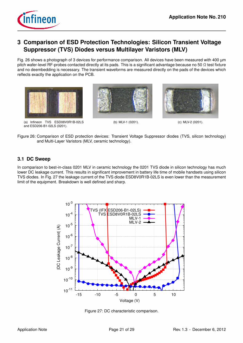
Fig. 26 shows a photograph of 3 devices for performance comparison. All devices have been measured with 400 µmpitch wafer-level RF-probes contacted directly at its pads. This is a significant advantage because no 50 Ω test fixtureand no deembedding is necessary. The transient waveforms are measured directly on the pads of the devices whichreflects exactly the application on the PCB.
(a) Infineon TVS ESD08V0R1B-02LSand ESD206-B1-02LS (0201).
(b) MLV-1 (0201). (c) MLV-2 (0201).
Figure 26: Comparison of ESD protection devices: Transient Voltage Suppressor diodes (TVS, silicon technology)and Multi-Layer Varistors (MLV, ceramic technology).
3.1 DC Sweep
In comparison to best-in-class 0201 MLV in ceramic technology the 0201 TVS diode in silicon technology has muchlower DC leakage current. This results in significant improvement in battery life time of mobile handsets using siliconTVS diodes. In Fig. 27 the leakage current of the TVS diode ESD8V0R1B-02LS is even lower than the measurementlimit of the equipment. Breakdown is well defined and sharp.
10-11
10-10
10-9
10-8
10-7
10-6
10-5
10-4
10-3
-15 -10 -5 0 5 10
|DC
Leakage C
urr
ent| (
A)
Voltage (V)
TVS (IFX ESD206-B1-02LS)TVS ESD8V0R1B-02LS
MLV-1MLV-2
Figure 27: DC characteristic comparison.
Application Note Page 21 of 29 Rev. 1.3 - December 6, 2012
Application Note No. 210
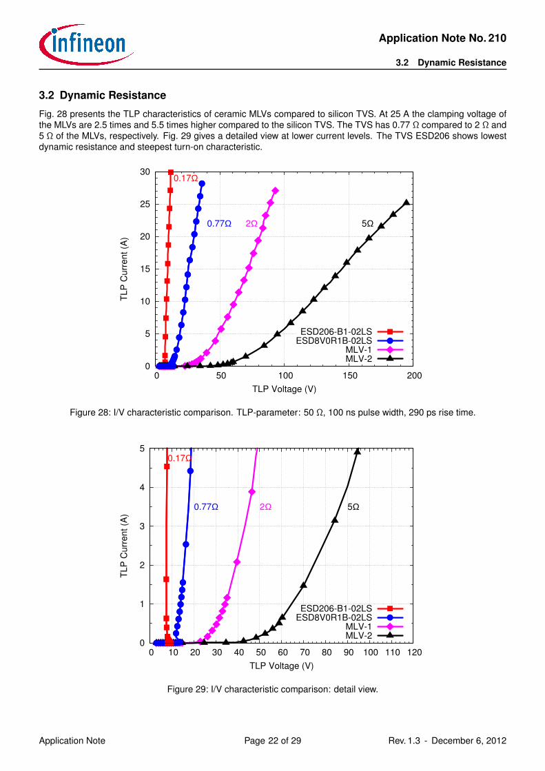
3.2 Dynamic Resistance
3.2 Dynamic Resistance
Fig. 28 presents the TLP characteristics of ceramic MLVs compared to silicon TVS. At 25 A the clamping voltage ofthe MLVs are 2.5 times and 5.5 times higher compared to the silicon TVS. The TVS has 0.77 Ω compared to 2 Ω and5 Ω of the MLVs, respectively. Fig. 29 gives a detailed view at lower current levels. The TVS ESD206 shows lowestdynamic resistance and steepest turn-on characteristic.
0
5
10
15
20
25
30
0 50 100 150 200
TLP
Curr
ent (A
)
TLP Voltage (V)
ESD206-B1-02LSESD8V0R1B-02LS
MLV-1MLV-2
0.17Ω
0.77Ω 2Ω 5Ω
Figure 28: I/V characteristic comparison. TLP-parameter: 50 Ω, 100 ns pulse width, 290 ps rise time.
0
1
2
3
4
5
0 10 20 30 40 50 60 70 80 90 100 110 120
TLP
Curr
ent (A
)
TLP Voltage (V)
ESD206-B1-02LSESD8V0R1B-02LS
MLV-1MLV-2
0.17Ω
0.77Ω 2Ω 5Ω
Figure 29: I/V characteristic comparison: detail view.
Application Note Page 22 of 29 Rev. 1.3 - December 6, 2012
Application Note No. 210
3.3 Transient Overshoot and Clamping Voltage
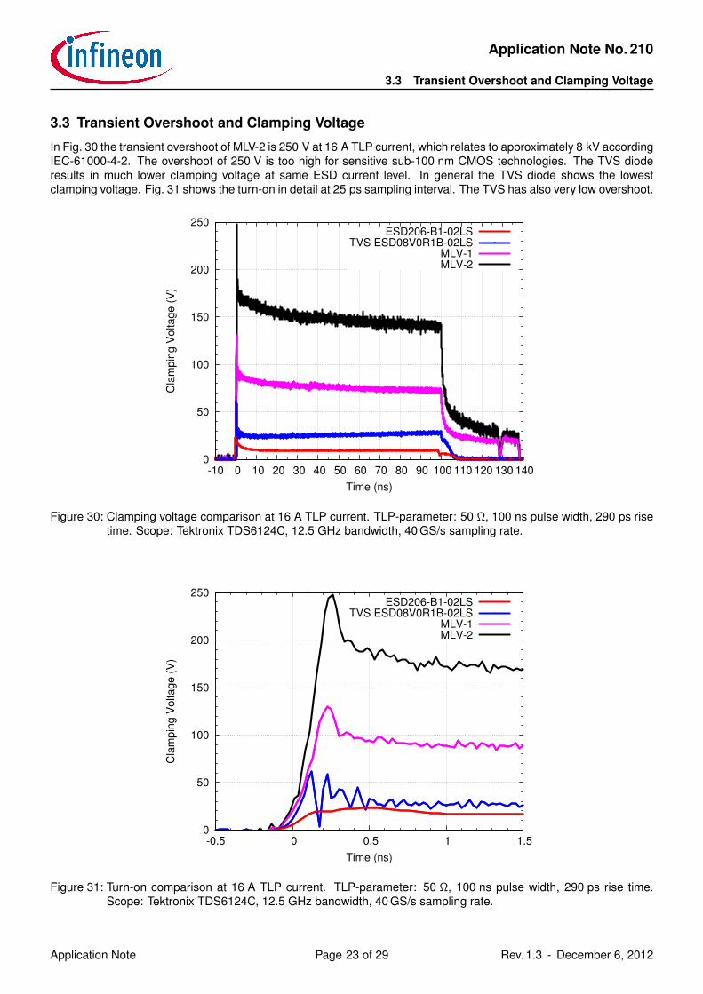
3.3 Transient Overshoot and Clamping Voltage
In Fig. 30 the transient overshoot of MLV-2 is 250 V at 16 A TLP current, which relates to approximately 8 kV accordingIEC-61000-4-2. The overshoot of 250 V is too high for sensitive sub-100 nm CMOS technologies. The TVS dioderesults in much lower clamping voltage at same ESD current level. In general the TVS diode shows the lowestclamping voltage. Fig. 31 shows the turn-on in detail at 25 ps sampling interval. The TVS has also very low overshoot.
0
50
100
150
200
250
-10 0 10 20 30 40 50 60 70 80 90 100 110 120 130 140
Cla
mpin
g V
oltage (
V)
Time (ns)
ESD206-B1-02LSTVS ESD08V0R1B-02LS
MLV-1MLV-2
Figure 30: Clamping voltage comparison at 16 A TLP current. TLP-parameter: 50 Ω, 100 ns pulse width, 290 ps risetime. Scope: Tektronix TDS6124C, 12.5 GHz bandwidth, 40 GS/s sampling rate.
0
50
100
150
200
250
-0.5 0 0.5 1 1.5
Cla
mpin
g V
oltage (
V)
Time (ns)
ESD206-B1-02LSTVS ESD08V0R1B-02LS
MLV-1MLV-2
Figure 31: Turn-on comparison at 16 A TLP current. TLP-parameter: 50 Ω, 100 ns pulse width, 290 ps rise time.Scope: Tektronix TDS6124C, 12.5 GHz bandwidth, 40 GS/s sampling rate.
Application Note Page 23 of 29 Rev. 1.3 - December 6, 2012
Application Note No. 210
3.4 Spot Leakage Drift
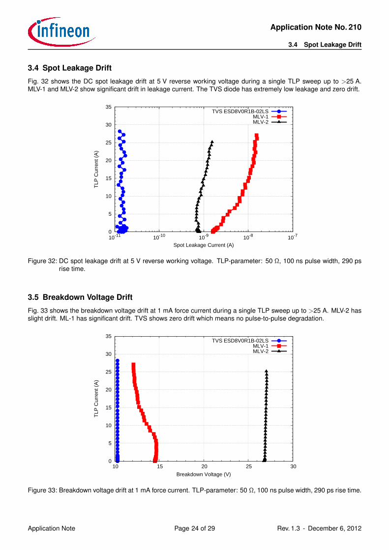
3.4 Spot Leakage Drift
Fig. 32 shows the DC spot leakage drift at 5 V reverse working voltage during a single TLP sweep up to >25 A.MLV-1 and MLV-2 show significant drift in leakage current. The TVS diode has extremely low leakage and zero drift.
0
5
10
15
20
25
30
35
10-11 10-10 10-9 10-8 10-7
TLP
Cur
rent
(A
)
Spot Leakage Current (A)
TVS ESD8V0R1B-02LSMLV-1MLV-2
Figure 32: DC spot leakage drift at 5 V reverse working voltage. TLP-parameter: 50 Ω, 100 ns pulse width, 290 psrise time.
3.5 Breakdown Voltage Drift
Fig. 33 shows the breakdown voltage drift at 1 mA force current during a single TLP sweep up to >25 A. MLV-2 hasslight drift. ML-1 has significant drift. TVS shows zero drift which means no pulse-to-pulse degradation.
0
5
10
15
20
25
30
35
10 15 20 25 30
TLP
Cur
rent
(A
)
Breakdown Voltage (V)
TVS ESD8V0R1B-02LSMLV-1MLV-2
Figure 33: Breakdown voltage drift at 1 mA force current. TLP-parameter: 50 Ω, 100 ns pulse width, 290 ps rise time.
Application Note Page 24 of 29 Rev. 1.3 - December 6, 2012
Application Note No. 210
3.6 Degradation due to Multi-Pulse Stress
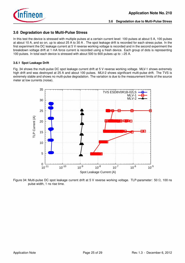
3.6 Degradation due to Multi-Pulse Stress
In this test the device is stressed with multiple pulses at a certain current level: 100 pulses at about 5 A, 100 pulsesat about 10 A, and so on, up to about 25 A to 30 A . The spot leakage drift is recorded for each stress pulse. In thefirst experiment the DC leakage current at 5 V reverse working voltage is recorded and in the second experiment thebreakdown voltage drift at 1 mA force current is recorded using a fresh device. Each group of dots is representing100 pulses. In total each device is stressed with about 500 to 600 pulses up to >25 A.
3.6.1 Spot Leakage Drift
Fig. 34 shows the multi-pulse DC spot leakage current drift at 5 V reverse working voltage. MLV-1 shows extremelyhigh drift and was destroyed at 25 A and about 100 pulses. MLV-2 shows significant multi-pulse drift. The TVS isextremely stable and shows no multi-pulse degradation. The variation is due to the measurement limits of the sourcemeter at low currents (noise).
0
5
10
15
20
25
30
35
10-11 10-10 10-9 10-8 10-7 10-6 10-5
TLP
Cur
rent
(A
)
Spot Leakage Current (A)
TVS ESD8V0R1B-02LSMLV-1MLV-2
Figure 34: Multi-pulse DC spot leakage current drift at 5 V reverse working voltage. TLP-parameter: 50 Ω, 100 nspulse width, 1 ns rise time.
Application Note Page 25 of 29 Rev. 1.3 - December 6, 2012
Application Note No. 210
3.6 Degradation due to Multi-Pulse Stress
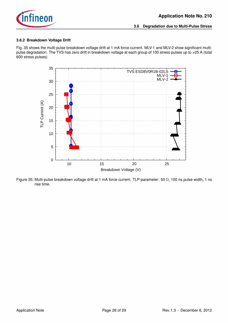
3.6.2 Breakdown Voltage Drift
Fig. 35 shows the multi-pulse breakdown voltage drift at 1 mA force current. MLV-1 and MLV-2 show significant multi-pulse degradation. The TVS has zero drift in breakdown voltage at each group of 100 stress pulses up to >25 A (total600 stress pulses).
0
5
10
15
20
25
30
35
10 15 20 25
TLP
Cur
rent
(A
)
Breakdown Voltage (V)
TVS ESD8V0R1B-02LSMLV-1MLV-2
Figure 35: Multi-pulse breakdown voltage drift at 1 mA force current. TLP-parameter: 50 Ω, 100 ns pulse width, 1 nsrise time.
Application Note Page 26 of 29 Rev. 1.3 - December 6, 2012
Application Note No. 210
References
References
[1] International Electrotechnical Commission, “Electromagnetic compatibility (EMC) - Part 4-2: Testing and mea-surement techniques - Electrostatic discharge immunity test”, 9th December 2008, ISBN 2-8318-1019-7,http://www.iec.ch/.
[2] International Electrotechnical Commission, “Electromagnetic compatibility (EMC) - Part 4-4: Testing and mea-surement techniques - Electrical fast transient/burst immunity test”, 8th July 2004, ISBN 2-8318-7567-6,http://www.iec.ch/.
[3] International Electrotechnical Commission, “Electromagnetic compatibility (EMC) - Electromagnetic compatibility(EMC) - Part 4-5: Testing and measurement techniques - Surge immunity test”, 29th November 2005, ISBN 2-8318-8371-7, http://www.iec.ch/.
[4] ANSI/ESDA/JEDEC, “ESDA/JEDEC Joint Standard for Electrostatic Discharge Sensitivity Testing - Human BodyModel (HBM) - Component Level”, April 2012, http://www.jedec.org/.
[5] A. Amerasekera, C. Duvvury, W. Anderson, H. Gieser and S. Ramaswamy, ESD in Silicon, John Wiley & Sons,Ltd, Baffins Lane, Chichester, West Sussex PO 19 1UD, England, 2 Edition, 2002.
[6] Albert Z. H. Wang, On-Chip ESD Protection for Integrated Circuits - An IC Design Perspective, Kluwer AcademicPublishers, 2002.
[7] JEDEC Solid State Technology Association, “Recommended ESD Target Levels for HBM/MM Qualification”,JEDEC Publication JEP155, August 2008, http://www.jedec.org.
[8] W. Simbuerger, D. Johnsson and M. Stecher, “High Current TLP Characterisation: An Effective Tool for theDevelopment of Semiconductor Devices and ESD Protection Solutions”, in ARMMS, RF & Microwave Society,November 2012, Invited.
[9] Electrostatic Discharge Association, “Electrostatic Discharge Sensitivity Testing - Transmission Line Pulse (TLP)- Component Level”, ANSI/ESD STM5.5.1-2008, May 19 2008.
[10] Electrostatic Discharge Association, “Electrostatic Discharge Sensitivity Testing - Very Fast Transmission LinePulse (VF TLP) - Component Level”, ANSI/ESD SP5.5.2-2007, November 12 2007.
[11] L. Espenschied and H.A. Affel, “U.S. Patent 1,835,031”, December 8 1931.
[12] D.J. Bradley, J.F. Higgins, M. H. Key and S. Majumdar, “A Simple Laser-triggered Spark Gap for Kilovolt Pulsesof Accurately Variable Timing”, Opto-Electronics Letters, vol. 1, pp. 62–64, 1969.
[13] T. Maloney and N. Khurana, “Transmission Line Pulsing for Circuit Modeling of ESD Phenomena”, in Proc. onEOS/ESD Symp., pp. 49–54, 1985.
[14] J. Barth, K. Verhaege, L.G. Henry and J. Richner, “TLP calibration, correlation, standards, and new techniques”,in Electrical Overstress/Electrostatic Discharge Symposium, pp. 85–96, 2000.
[15] J. Barth, K. Verhaege, L.G. Henry and J. Richner, “TLP calibration, correlation, standards, and new techniques”,Electronics Packaging Manufacturing, vol. 24, n. 2, pp. 99–108, 2001.
[16] GGB Industries, Inc., http://www.ggb.com/, 2012.
[17] Tektronix, Test and Measurement Equipment, http://www1.tek.com/, 2012.
[18] H. A. Gieser and M. Haunschild, “Very-Fast Transmission Line Pulsing of Integrated Structures and the ChargeDevice Model”, in Proceedings of EOS/ESD Symposium, 1996.
[19] E. Grund, “Deriving the DUT Current and Voltage Waveforms by Merging VF-TLP Incident and Reflected Sig-nals”, EOS/ESD/EMI-Workshop, organized by M. Bafleur LAAS, Toulouse, F, 2006.
[20] Evan Grund and Robert Gauthier, “TLP Systems with Combined 50 and 500-ohm Impedance Probes and KelvinProbes”, in proceedings of EOS/ESD Symposium, pp. 127–136, 2003.
[21] N. Shammas, D. Chamund and P. Taylor, “Forward and reverse recovery behaviour of diodes in power converterapplications”, in 24th International Conference on Microelectronics, volume 1, pp. 3–10, 16-19 May 2004.
[22] “MIL-STD-750D, Method 4031.3, Reverse Recovery Characteristics”.
[23] “MIL-STD-750D, Method 4026.3, Forward Recovery Voltage and Time”.
Application Note Page 27 of 29 Rev. 1.3 - December 6, 2012

Application Note No. 210
References
[24] AVTECH Electrosystems LTD, “A Comparison of Reverse Recovery Measurement Systems”, Technical report,November 2006.
[25] Michael Reisch, Elektronische Baulemente, Springer, 2 Edition, 2007.
[26] MathWorks - MATLAB and Simulink for Technical Computing, http://www.mathworks.com/, 2012.
Author
Werner Simbürger
Copyright Notice
Section 2 is partially reprint of the publication [8] with granted permission by the ARMMS RF & Microwave Society,19th to 20th November 2012 at Wyboston Lakes, Wyboston, UK.
Application Note Page 28 of 29 Rev. 1.3 - December 6, 2012

w w w . i n f i n e o n . c o m
Published by Infineon Technologies AG