all digital fm demodulator kartik nair · design intends to implement a fm demodulator for...
TRANSCRIPT

All Digital FM Demodulator
Kartik Nair
Thesis submitted to the faculty of the Virginia Polytechnic Institute and State University in partial
fulfillment of the requirements for the degree of
Master of Science
In
Electrical Engineering
Dong S. Ha, Chair
Yang (Cindy) Yi
Xiaoting Jia
August 15, 2019
Blacksburg, Virginia
Keywords: FM Demodulator, Quadrature Demodulator, FPGA
Kartik Nair

All Digital FM Demodulator
Kartik Nair
ABSTRACT
The proposed demodulator is an all-digital implementation of a FM demodulator. The proposed
design intends to implement a FM demodulator for high-speed applications, which makes the
requirements for analog components minimal. The proposed circuit is an all-digital quadrature
demodulator, where the individual components have been implemented without using any
multipliers. The topology uses a Pulse width modulation (PWM) block to avoid the need for a DAC.
The Xilinx virtex-7 FPGA has been used as the reference device for the work. The circuit is
validated through behavioral simulations and the results conclude the proposed circuit demodulates
the targeted FM channel and provides the spectrum information for the targeted FM channel.
All Digital FM Demodulator
Kartik Nair
GENERAL AUDIENCE ABSTRACT
With the rise in popularity of reconfigurable hardware, such as FPGAs, digital signal processing has
become one of the most widespread usage of such devices. The major advantage of using FPGAs for
implementing signal processing algorithms is that they provide very less time to market and can be
re-modeled or modified in easily. Moreover, the netlists designed for FPGAs can be easily translated
to ASICs.
As wireless communication has become omnipresent, modulation and demodulation schemes
have become an area of great interest. With the increase in data rates for the modern-day
communication systems, the digital implementation of these algorithms is becoming more and more
common. This is further aided by the advancements in high-speed ADCs and the Electronic Design
Automation (EDA) tools, which have made the usage of FPGAs lot more feasible and a lot more
efficient.
This work discusses the demodulation scheme for one of the most widespread modulation
algorithms, Frequency Modulation (FM). An all-digital FM demodulator design is proposed for high-
speed implementation on FPGAs. The proposed design is an all-digital quadrature I-Q based
demodulator.

iv
Acknowledgements
I would like to thank my advisor, Dr. Dong S. Ha, for his immense support, guidance and
patience. Dr. Ha’s guidance helped me find my interest and give a direction to my career. I would
also like to thank Dr. Yang (Cindy) Yi and Dr. Xiaoting Jia for their co-operation and for being there
whenever I needed them.
I would like to thank the Bradley Department of Electrical and Computer Engineering at
Virginia Tech for providing me the opportunity to get my education at such a great school and help
me develop great skills and character through my master’s.
My sincerest thanks to my colleagues at the MICS lab: Junjie Wang, Jiayu Li, Alanté Dancy,
Keyvan Ramezanpour, Brannon Kerrigan, Long Huang and Fairborz Lohrabi Pour. Thank you for
always being helpful. I wish you all the best for your future.
I thank God for always giving me the strength and belief to overcome everything. I am
forever grateful to my mother, Ms. Sreekala Nair, my father, Mr. G. Radhakrishnan Nair, my brother
Suchit Nair and my entire family. Without their support and sacrifice it would have been impossible.
I am also thankful to my girlfriend, Anulika Ugwueze, for supporting me through everything and
always motivating me to get better.
I have had the opportunity to make some great friends during my time here and I am ever so
grateful for all their help.

v
Table of Contents
ABSTRACT.......................................................................................................................................... ii
GENERAL AUDIENCE ABSTRACT.......................................................... ...................................... iii
Acknowledgements .............................................................................................................................. iv
Table of Contents ................................................................................................................................... v
List of Figures .................................................................................................................................... vii
List of Tables ........................................................................................................................................ ix
Chapter 1: Introduction .......................................................................................................................... 1
1.1 Motivation ........................................................................................................................... 1
1.2 Scope of the Proposed Research ......................................................................................... 1
1.3 Proposed Approach and Technical Contributions ............................................................... 2
1.4 Organization of this Thesis ................................................................................................. 3
Chapter 2: Preliminaries ........................................................................................................................ 4
2.1 Pre-requisite ........................................................................................................................ 4
2.1.1 Broadcast FM................................................................................................................ 4
2.1.2 Conventional Analog FM Demodulator ........................................................................ 5
2.2 Previous Designs………………………………….............................................................. 6
2.3 Fixed-point Arithmetic ….................................................................................................... 6
2.4 Chapter Summary ................................................................................................................ 7
Chapter 3: Proposed Work……………………… ................................................................................. 8
3.1 Design Specification…………………... ............................................................................ 8
3.2 Design Implementation……………….. ............................................................................. 9
3.2.1 CIC Decimator............................................................................................................. 10

vi
3.2.2 Sine/Cosine Generator ................................................................................................ 12
3.2.3 ARCTAN .................................................................................................................... 15
3.2.4 Phase-Frequency Conversion....................................................................................... 18
3.2.5 Pulse Width Modulation (PWM)................................................................................. 18
3.3 Design Overview............................................................................................................... 19
3.4 Chapter Summary .............................................................................................................. 21
Chapter 4: Simulation and Verification................................................................................................ 22
4.1 Implementation Requirements........................................................................................... 22
4.1.1 Target FPGA ............................................................................................................... 22
4.1.2 Implementation Environment...................................................................................... 23
4.1.3 Design Flow................................................................................................................. 23
4.2 Block Simulations ............................................................................................................. 24
4.2.1 CIC Decimator ............................................................................................................ 24
4.2.2 Sine/Cosine Generator................................................................................................. 26
4.2.3 ARCTAN..................................................................................................................... 27
4.2.4 Phase-Frequency Convertor......................................................................................... 29
4.2.5 Pulse Width Modulation.............................................................................................. 29
4.3 Demodulated FM Spectrum............................................................................................... 30
4.4 Chapter Summary .............................................................................................................. 31
Chapter 5: Conclusion.......................................................................................................................... 32
5.1 Proposed Research and Contributions……....................................................................... 32
5.2 Future Goals ...................................................................................................................... 33
Appendix.............................................................................................................................................. 34
A. Block Netlists...................................................................................................................... 34
References ........................................................................................................................................... 38

vii
List of Figures
Figure 2-1: Typical baseband spectrum for FM..................................................................................... 5
Figure 2-2: Conventional analog quadrature demodulator..................................................................... 6
Figure 2-3: Fixed-point representation................................................................................................... 7
Figure 3-1: Digital FM radio setup......................................................................................................... 9
Figure 3-2: Proposed all digital FM demodulator.................................................................................. 9
Figure 3-3: Architecture of CIC decimator.......................................................................................... 11
Figure 3-4(a): Stage I CIC decimator magnitude response.................................................................. 11
Figure 3-4(b): Stage II CIC decimator magnitude response................................................................. 12
Figure 3-5: Implementation of sine/cosine generator........................................................................... 13
Figure 3-6: Quarter wave symmetry of sine wave ............................................................................... 13
Figure 3-7: Increment (M) decides the rate at which we cycle through the
LUT…………………………………………………………………….............................................. 14
Figure 3-8: Vectoring mode of operation for CORDIC........................................................................ 16
Figure 3-9: PWM implementation ...................................................................................................... 18
Figure 3-10: Block diagram of the proposed design ............................................................................ 20
Figure 4-1: FPGA development design flow....................................................................................... 24
Figure 4-2(a): Expected step response................................................................................................. 25
Figure 4-2(b): Step response of implemented design........................................................................... 25
Figure 4-3: 98.7MHz sinusoidal output............................................................................................... 26
Figure 4-4: Effect of phase accumulator on output frequency………….............................................. 27
Figure 4-5: Behavior of ARCTAN module......................................................................................... 28
Figure 4-6: Phase-Frequency Relationship.......................................................................................... 29
viii
Figure 4-7: PWM output...................................................................................................................... 30
Figure 4-8: 100KHz demodulated FM spectrum................................................................................. 30
Figure 4-9: Mono audio spectrum for demodulated channel............................................................... 31
Figure A-1: CIC Decimator………………………………................................................................. 34
Figure A-2: Sine/cosine generator...…...…………………................................................................. 35
Figure A-3: ARCTAN……………………………………................................................................. 35
Figure A-4: Phase-frequency convertor……………..……................................................................. 36
Figure A-5: PWM block….………………………………................................................................. 36

ix
List of Tables
Table 1: Design specifications................................................................................................................ 8
Table 2: CIC decimator specifications ................................................................................................. 10
Table 3: ATAN angles used for vector rotation…...………………………......................................... 17
Table 4: Duty cycle for PWM output………………...………………………..................................... 19
Table 5: ARCTAN output……………………………..……………………...................................... 28

1
Chapter 1
Introduction
1.1 Motivation
In recent years, a lot of progress has been made in the field of high-speed ADCs. The sampling
rates of ADC have touched the range of Giga samples per second (GSPS). The advent of such high-
speed ADCs has seen the rise of direct RF sampling radio architectures. These architectures enable us
to shift the design to the digital domain from the conventional RF/analog domain.
This shift to the digital domain, enabled by high-speed ADCs, eliminates the need for analog
filters. Also, the digital implementation makes the design more robust towards noise. Implementing
the design on a reconfigurable platform, such as a FPGA, provides additional benefits of cost
effectiveness, less time to market and easy remodeling. The netlists generated for the FPGAs can also
be easily translated to ASIC designs.
This work aims at providing a FM demodulator design that can be implemented onto the
FPGAs and can provide the demodulated FM spectrum information.
1.2 Scope of the Proposed Research
FM is one of the most common and most widespread RF standards. In a FM modulated signal,
the information of the baseband signal alters the frequency characteristics of a high-frequency carrier.
At the receiver’s end, the frequency information from the modulated signal is extracted and the original
message signal is reconstructed to get a discernable output.
Most commonly, the FM demodulators were implemented in the analog domain. Several
schemes are available for the same, such as a quadrature detector, Phase-Locked Loop (PLL) detector,
Foster-Seeley discriminator and ratio detector.
However, in digital domain, two of the most common schemes to implement a FM demodulator
are: PLL based demodulator and a quadrature demodulator. A PLL based architecture is a coherent

2
demodulator that tracks the input signal and generates an error signal, that is used as the demodulated
output. It provides superior performance; however, it presents more complexity. [1,2,3] discuss the
architectures for an all-digital PLL (ADPLL). An ADPLL architecture can be used for FM
demodulation implementation on FPGAs. On the other hand, a quadrature demodulator is a non-
coherent demodulator. It extracts the phase information from a FM signal and uses the phase
information to extract the message signal. [3,4] discuss the FPGA implementation of I-Q
based/quadrature architecture for demodulation applications.
This work focuses on a quadrature/I-Q based FM demodulator design where the use of
multipliers is avoided for individual functional blocks, as adders or subtractors are faster and easier to
implement.
1.3 Proposed Approach and Technical Contributions
An all-digital FM demodulator is designed for high-speed applications. The major contribution
of the work is to implement the demodulation scheme without using any multipliers for filtering,
sinusoidal generation and phase detection. The work uses the pulse width modulation (PWM) to
generate the output, hence, avoiding the use of a DAC.
Typically for a digital implementation of a demodulator, certain portions are implemented as
part of the analog frontend, such as filtering, down-conversion or even decimation. According to
Nyquist theorem, the data must be sampled at a frequency at least twice the bandwidth (Nyquist rate),
for possible reconstruction of the signal. If a signal is sampled close to its Nyquist rate, the need for
analog filters become stringent. However, the modern-day high-speed ADCs have sampling rates in
the GSPS range. These high sampling rate ADCs sample the input data at a much higher frequency
than twice the bandwidth of the signal.
The main contribution of this project is to carry out filtering and down-conversion in the digital
domain. This results in a minimal or no analog frontend.
The proposed design was written using the Verilog hardware description language (HDL) and
simulated using ModelSim and icarus verilog. The simulated results were plotted using MATLAB.
The netlist for the modules were generated using Xilinx Vivado 2019.2, for a Xilinx Virtex-7 FPGA.
The input data used to verify the modules was captured using a AD9689 ADC.

3
1.4 Organization of this Thesis
The organization of this thesis is as follows. Chapter 2 discusses the preliminary concepts
required to understand the work. The chapter goes through the various topologies used in previous
works to implement digital FM demodulators. It also talks about certain concepts that are crucial to the
work. Chapter 3 gets into the proposed design, starting with the specifications for the design. The
working and implementation of individual blocks is discussed in this section. Implemented block
diagrams for the individual blocks are shown for the blocks. Chapter 4 provides the behavioral
simulation results for the blocks and verification results for each block. The netlist generated for the
blocks is also presented. Chapter 5 concludes the thesis by going through the lessons learned from this
work and discussing some future goals for the work.
4
Chapter 2
Preliminaries
This chapter provides the basic knowledge about the broadcast FM and previous digital FM
demodulator design. The following information is intended to make the proposed work and
contributions of the work more comprehensive. Section 2.1 details the basics of broadcast FM and
conventional I-Q demodulator. Section 2.2 explains the implementations that have been used in
previous works. Section 2.3 explains an important concept of fixed-point arithmetic and Section 2.4
summarizes the chapter.
2.1 Pre-requisite
2.1.1 Broadcast FM
FM broadcasting is a radio broadcasting technology based on frequency modulation. It was an
upgrade over AM broadcasting, since it provided a higher quality broadcast. The standard FM spectrum
is a subset of VHF frequency spectrum and ranges from 88MHz to 108MHz. As per the definition of
frequency modulation, the frequency deviation of a carrier varies depending on the amplitude of the
modulating baseband signal. In case of FM broadcasting, the maximum frequency deviation is ±
75KHz. Typical spectrum for a baseband signal transmitted through FM is shown in Figure 2-1.

5
Figure 2-1: Typical baseband spectrum FM.
This work focuses on extracting the mono audio (left + right) information spectrum for a
desired channel.
2.1.2 Conventional Analog FM Demodulators
For a FM signal, the amplitude of the baseband message signal causes the frequency deviation
for a high frequency carrier. Hence, to demodulate a FM signal, the demodulator should be able to
extract the amplitude information from the frequency variations of the received signal.
Two of the most popular FM demodulation techniques are a PLL based demodulator and a
quadrature demodulator. A PLL demodulator is a coherent detector, whereas a quadrature detector is
non-coherent detector. A quadrature demodulator is easier to implement, and it is easier to ensure its
performance. Both [5,6] have discussed the quadrature demodulator in detail. The reference design of
a conventional quadrature demodulator can be seen in Figure 2-2.

6
Figure 2-2: Conventional analog quadrature detector.
2.2 Previous Designs
Various topologies have been adopted to enable FPGA implementation of a digital
demodulator. In this section, we are going to look into two such topologies. [7] discusses a mixed
demodulator topology for FM demodulation. In this work, the design is divided into three parts: a
quadrature mixer, FM demodulator and an output filter.
The purpose of the quadrature mixer is to generate the I and Q components from an input FM
signal. A look-up table (LUT) method has been used to generate the sine and cosine components.
The second stage is a FM demodulator. The FM demodulator is implemented using a mixed
demodulator. A mixed demodulator composes of a delay demodulator and a phase adapter
demodulator [9]. The final stage, low pass filtering, is implemented as an IIR filter.
[8] has proposed a design that uses I-Q demodulator along with an analog front end for
extracting demodulated FM spectrum and getting RBDS information. An analog filter is used to
obtain the IF and then the IF is passed to the ADC. The digitized data is fed to a I-Q demodulator.
2.3 Fixed-Point Arithmetic
One of the concepts that has been used throughout the design is fixed-point arithmetic. To
make the design more accurate, it important to be able to work with fractional numbers. However, a
binary word only represents integers. Fixed-point arithmetic allows us to be able to represent fractional
numbers in form of binary words.

7
A fixed-point binary number is represented as “<W,L>”. Where,
W = Word width
L = Fractional bits
A binary fixed-point number can be interpreted to have the binary point after ‘L’ bits from the
LSB, as seen through the example shown in Figure 2-5. The remaining W-L bits denote the integer
part.
W=16L=8
Figure 2-3: Fixed-point representation
2.4 Chapter Summary
In this chapter, the preliminary concepts related to this work were introduced. The FM
broadcasting was discussed, and the FM spectrum was shown. Furthermore, we looked at conventional
analog FM demodulator. Moving on, two previous design for digital FM demodulators were looked at
and their implementation was studied. To conclude the chapter, an important concept of fixed-point
arithmetic was discussed.

8
Chapter 3
Proposed Work
This chapter discusses in detail the proposed all-digital FM demodulator. The all-digital design
is an I-Q demodulator, with minimal or no analog frontend (a LNA may or may not be required
depending on the receiving antenna). A high-speed ADC is used to digitize the received FM signal.
The signal is then fed to the proposed FM demodulator on the FPGA. The high-speed serial data from
the ADC is decimated and then I and Q components are generated for the data. An ARCTAN method
is used to extract the phase information from the I and Q components. The phase information is then
used to obtain the frequency information of the signal.
3.1 Design Specifications
The specifications of the proposed design are as listed in Table 1.
Table 1: Design Specifications
Specification Requirement
ADC Sampling Rate 2.56 GHz
Frequency Range 88 MHz – 108 MHz
Data Format <16,14>
The ADC is a high-speed ADC that samples the FM signal at a rate of 2.56 GHz. The sampled
data is input to the FPGA in the <16,14> format, through a high-speed serial interface. The target
frequency range for the design is 88MHz-108MHz. For this work, the design is made specific to the
98.7 MHz channel. The design demodulates and presents the frequency spectrum for this channel. The
data is in 2’s compliment, <16,14> fixed-point format.

9
3.2 Design Implementation
The proposed design is implemented on the FPGA. This implemented design would be part of
the FM receiver setup. The entire radio receiver will look similar to what is shown in Figure 3-1. As
the ADC has a very high sampling rate of 2.56GHz, it is able to capture a wide bandwidth of data.
Also, since the FM band is highly oversampled, the analog front end can be implemented without using
an analog filter. Oversampling relaxes the need for an analog filter with stringent design requirements.
Audio
Output
FM Demodulator
(FPGA)14-bit ADCLNA
Serial
Interface
14 16
Figure 3-1: Digital FM Radio Setup
The sampled data from the ADC is passed through a high-speed serial interface that follows
the JESD204B serial protocol. Hence, the data available to the proposed FM demodulator is in
<16,14> format.
Figure 3-2 presents the block diagram of the proposed all digital FM demodulator. The input
data is decimated using a cascaded integrator-comb (CIC) decimator before the I and Q components
are generated for the input FM signal.
Figure 3-2: Proposed All Digital FM Demodulator

10
The decimated input signal represents a wide band of spectrum. To obtain the information for
the 98.7 MHz channel, the data is down converted. The down conversion is carried out by
multiplying the signal through a sinusoidal of 98.7 MHz. After down conversion, the 98.7 MHz
signal can be seen as a baseband signal. A low pass filter is used on the down converted signal to
extract the information from the 98.7 MHz channel and reject the undesired spectrum information.
Once the baseband channel is isolated, the I and Q components of the signal are used to find
out the phase of the signal. The difference relationship between the phase and frequency is then used
to obtain the frequency of the signal. The following sub-sections go through individual blocks of the
design.
3.2.1 CIC Decimator
In modern day DSP architectures, CIC filters have become quite prominent. CIC
decimators or interpolators can be implemented using adders and subtractors only. The lack of
multipliers makes them preferable for high speed applications. This architecture is studied in great
detail in [10-14].
The specifications of the CIC decimators used for this design are as shown in table 2.
Table 2: CIC Decimator Specifications
Parameters Stage I Stage II
Decimation Factor (R) 8 16
Differential Delay (M) 1 10
Number of stages (N) 1 1

11
Figure 3-3 shows the basic structure of a CIC decimator. The integrator part always works at
the higher frequency, while the comb section always operates at the lower frequency. The output
frequency of a CIC decimator is the lower frequency, reduced by the factor ‘R’. Hence, the CIC
decimator carries out low pass filtering, as well as down sampling.
Figure 3-3: Architecture for CIC Decimator.
The magnitude response of the two CIC decimators can be seen in Figure 3-4(a) and 3-4(b).
Figure 3-4(a): Stage I CIC Decimator Magnitude Response.

12
Figure 3-4(b): Stage II CIC Decimator Magnitude Response.
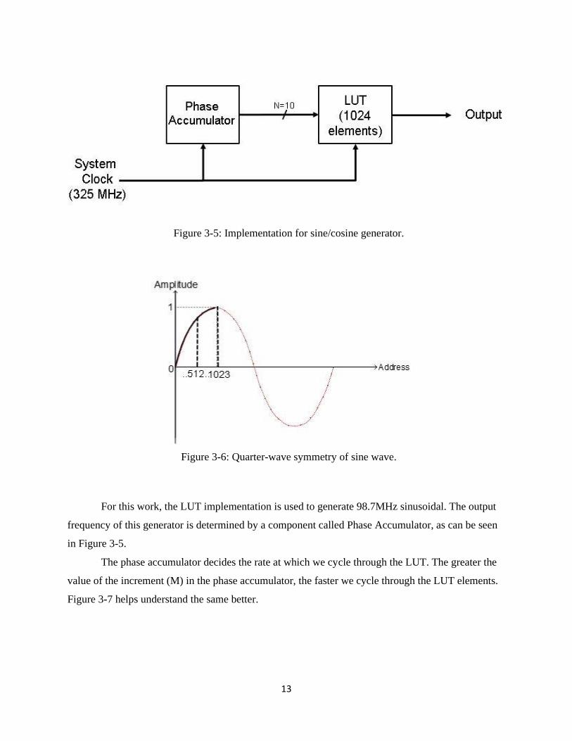
3.2.2 Sine/Cosine Generator
The sine/cosine generator block is a digital equivalent of a local oscillator. Digital
implementation of a waveform generator is known as a Digital Direct Synthesis (DDS). The purpose
of this block is to generate the 98.7MHz sinusoidal. The input signal is down converted using these
sinusoidal.
With the rise of DSP, DDS has become an area of great research. Waveform generation is a
critical part of many DSP applications. The ability to generate a sinusoidal is very important for
implementation of modulation and demodulation schemes on a FPGA.
Two of the most popular methods of generating sinusoids in digital systems are a LUT based
method or a COordinate Rotation DIgital Computer (CORDIC) based method. For this work, a LUT
based method is used. The LUT based method allows for a faster implementation with less circuit
complexity. Figure 3-5 shows the LUT implementation for this work.
As can be seen in Figure 3-6, only a quarter of the sine wave is stored in the LUT, using 1024
elements. Entire sine wave can be generated using any quarter of a sine wave, this property of the
sine waveform is called quarter wave symmetry. Exploiting the quarter wave symmetry of the sine
wave allows for a better resolution and smaller size LUT implementation.
13
Figure 3-5: Implementation for sine/cosine generator.
Figure 3-6: Quarter-wave symmetry of sine wave.
For this work, the LUT implementation is used to generate 98.7MHz sinusoidal. The output
frequency of this generator is determined by a component called Phase Accumulator, as can be seen
in Figure 3-5.
The phase accumulator decides the rate at which we cycle through the LUT. The greater the
value of the increment (M) in the phase accumulator, the faster we cycle through the LUT elements.
Figure 3-7 helps understand the same better.
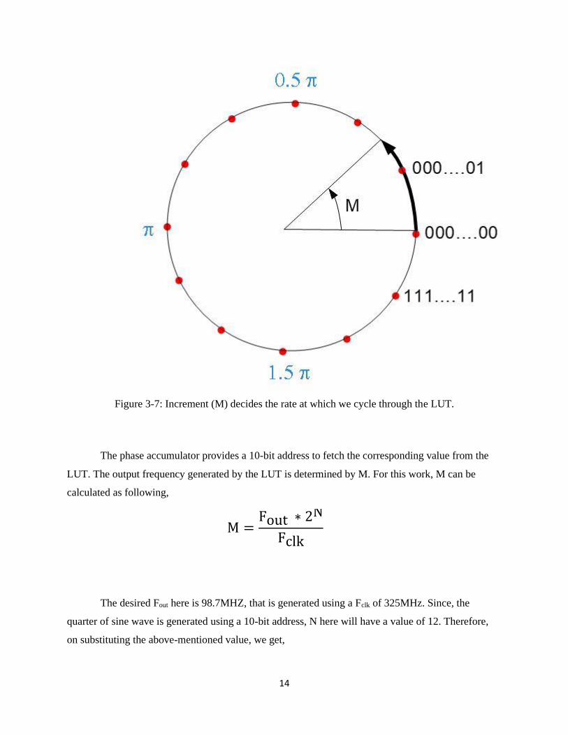
14
Figure 3-7: Increment (M) decides the rate at which we cycle through the LUT.
The phase accumulator provides a 10-bit address to fetch the corresponding value from the
LUT. The output frequency generated by the LUT is determined by M. For this work, M can be
calculated as following,
The desired Fout here is 98.7MHZ, that is generated using a Fclk of 325MHz. Since, the
quarter of sine wave is generated using a 10-bit address, N here will have a value of 12. Therefore,
on substituting the above-mentioned value, we get,
M =Fout ∗ 2
N
Fclk

15
M = 1263.36 ≈ 1263
With M = 1263, the LUT will generate a 98.7MHZ sinusoidal with an input clock of
325MHz.
3.2.3 ARCTAN
Once the I and Q components are generated by multiplying the decimated input with the
sine/cosine of desired frequency, they are passed through a channel select filter. For this work, stage
II CIC decimators carry out the functioning of channel selection. The phase information can be
extracted from the baseband I and Q components obtained after the channel select filters.
To extract the phase information, an arctan (tan-1) function must be implemented in hardware.
[8] implements a ROM based arctan. The MSB of I and Q components decide the input address for a
arctan ROM. The input address then returns the arctan for corresponding I and Q values. However,
the problem with this method is that the size of the ROM increases as we want to achieve a better
performance. For this work, a CORDIC algorithm based implementation has been used.
The implementation and analysis of CORDIC algorithm has been a widespread topic for
research. The ability to implement various trigonometric functions makes it a very viable tool.
CORDIC can be implemented on the hardware using various topologies [21-23], however, a state-
machine based approach is implemented in this work.
CORDIC has two modes of operation: Rotational mode and Vectoring mode. For arctan
implementation, vectoring mode of operation is used. In this arctan implementation, input I and Q
components represent a vector. A pre-rotation is carried out initially to rotate and bring the vector
between 𝝅
𝟐 𝒕𝒐
−𝝅
𝟐. After the pre-rotation, a state-machine is used to iteratively rotate the vector
towards x-axis, as can be seen in the example shown in Figure 3-8.

16
Figure 3-8: Vectoring Mode of Operation for CORDIC.
The vectoring mode of operation can be summarized by following equations,
Xi+1 = Xi – Yi . Di . 2-i
Yi+1 = Yi + Xi . Di . 2-i
Zi+1 = Zi – Di . Tan-1(2-i)
In the above mentioned equations, X and Y represent I and Q information, while Z represents
the phase. D represents the direction of rotation for the vector, such that,
For each iteration, the vector is rotated by an angle tan-1(2-i). The value of these roation
angles is stored in ROM, in a <20,8> signed fixed point format. Table 3 shows the angle values
stored in the ROM.

17
Table 3: Atan angles used for vector rotations.
i
2-i
Angle (deg)
{Tan-1(2-i)}
1 1/2 45
2 1/4 26.56
3 1/8 14.04
4 1/16 7
5 1/32 3.57
6 1/64 1.78
7 1/128 0.89
8 1/256 0.44
For each I and Q value, 8 iterations are required to obtain the arctan(Q/I). This allows us to
obtain a fairly accurate result, since a CORDIC algorithm generate an accurate result within 8 cycles.

18
3.2.4 Phase – Frequency Converter
Once the phase information is obtained through the arctan block, it is converted into the
frequency information. To obtain the frequency, the difference relationship between phase and
frequency is exploited, as seen in the equation below,
ω = 𝒅Φ
𝒅t≈
∆Φ
∆t
If ∆t = 1,
ω = Φi+1 – Φi
3.2.5 Pulse Width Modulation (PWM)
A PWM block is used at the end of the phase-frequency converter. This PWM block drives a
GPIO pin of the FPGA that can be used to drive additional circuit to produce an audio output. [24]
talks about how the PWM block can be used to alter the mean DC value and hence emulate an analog
signal. Moreover, [25] discusses the application of PWM for audio generation.
For this work, the PWM is implemented using a reference counter and a comparator, as
shown in Figure 3-9.
Figure 3-9: PWM Implementation.

19
The PWM block accepts a 4 MSB bits of the frequency word and generates a varying duty
cycle based on the input word, as seen in table 4.
Table 4: Duty Cycle for PWM Output
Frequency Word
Duty Cycle
15 100
7 75
3 50
1 25
The PWM output is high as long as the reference counter value is less than the input
frequency word. As the reference counter exceeds the value of the input frequency word, the PWM
output becomes low.
3.3 Design Overview
The overall block diagram of the proposed design can be seen in Figure 3-10.

20
Figure 3-10: Block Diagram of the Proposed Design.
The input data is obtained from a high-speed serial interface. The data is then decimated
using stage I CIC decimator. The decimated data is then down converted using a DDS producing the
frequency equal to the carrier frequency of the target FM channel, 98.7 MHz. The down converted
data is passed through another CIC decimator to isolate the desired channel. The channel bandwidth
is around 100Khz and hence the stage II CIC decimator can bring down the signal to a few MHz
The arctan block is then used to extract the phase information from the decimated data, this
phase information is converted to frequency information using a phase-frequency converter. A PWM
block is used to generate the signal to drive the output GPIO pin.

21
3.4 Chapter Summary
This chapter intends to introduce the proposed design for an all-digital FM demodulator. The
major achievements of the design are:
o No multipliers used for individual blocks
o Filtering, decimation and down conversion are all carried out in digital
domain
o The design allows for a minimal analog frontend.
o PWM output intends to avoid usage of additional DAC.
The proposed design is a quadrature FM demodulator. It uses an arctan based phase
detection, which is useful in obtaining the frequency information.

22
Chapter 4
Simulation and Verification
This chapter discusses the simulation results for the design blocks and the entire design. Certain
assumptions have been made with regards to the input data for this design, and that have been
mentioned in this section.
Various tools used for the implementation of this work are specified in this section. Also, the
design flow associated with this work, shown in this section, helps us understand the implementation
procedure better.
4.1 Implementation Requirements
4.1.1 Target FPGA
The implementation of this design has been studied for a Xilinx Virtex-7 FPGA.
Virtex-7 FPGA series belongs to a series of high-speed FPGAs. The features of the virtex-7, that make
it a good option, are mentioned as follows:
• Up to 2 million logic cells
• 28nm process technology
• 88 high-speed serial transceivers
• Transceiver speed = 28.05 Gb/s

23
4.1.2 Implementation Environment
As discussed earlier, the input data for this work is considered to be in <16,14> format.
It is assumed that the input sampled data is obtained from a high-speed ADC, AD9689. Some relevant
features of AD9689 are as follows:
• 2.56 Giga samples/ second
• Full-scale voltage = 1.1 Vp-p
• JESD204B coded serial output
JESD204B is a high-speed serial interface that has gained popularity with high-speed ADCs.
It is implemented as an IP core for FPGAs; hence, its implementation was out of the scope of this
proposed work.
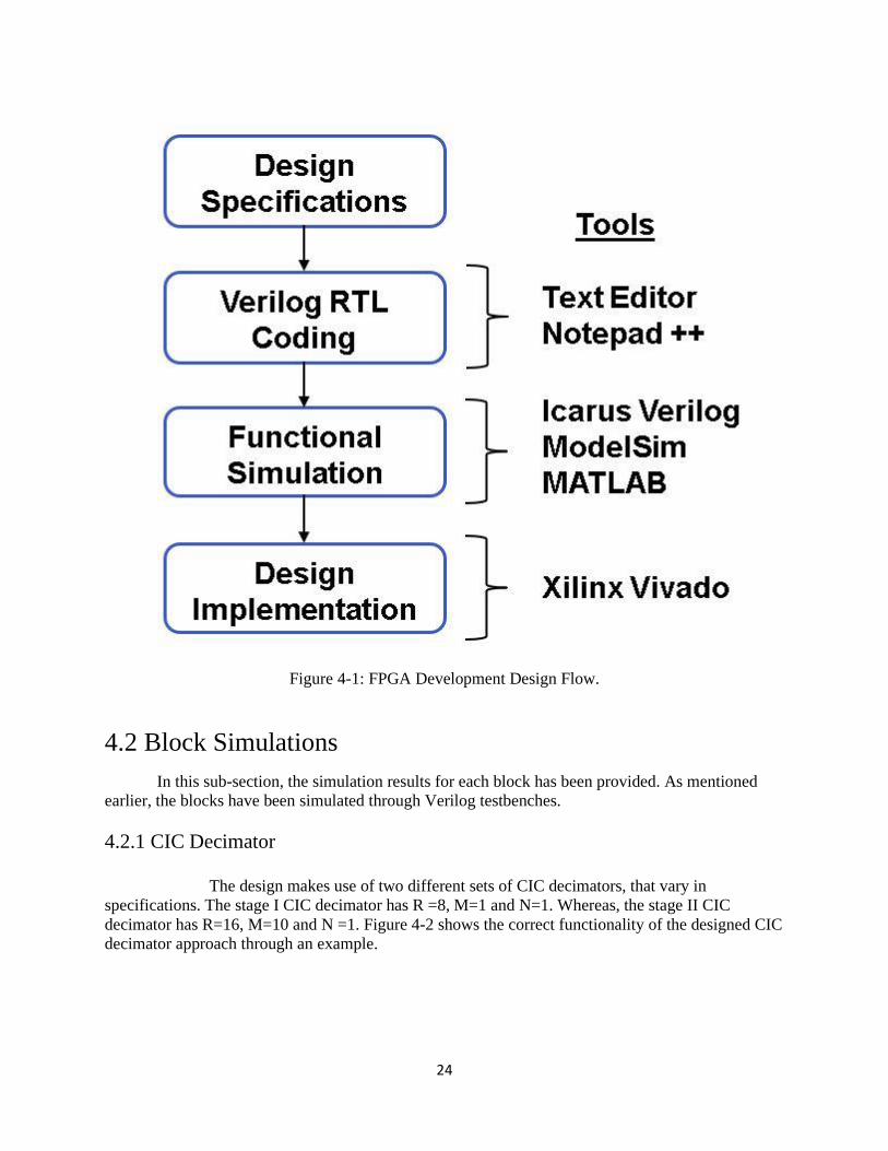
4.1.3 Design Flow
The design flow for the work starts with setting up the target specifications for the design, as
seen in Figure 4-1. Once the target specifications are set, the RTL coding for the blocks are carried out.
Verilog HDL is used for RTL coding and a text editor is the only requirement for this stage. Alongside
the RTL coding, Verilog testbenches are also written for each block. These testbenches are necessary
for behavioral simulation of the blocks. The Verilog testbenches are simulated using Icarus Verilog
and ModelSim. The results are exported to manually to MATLAB for plotting. The simulation
waveforms are viewed with the help of GTKwave waveform viewer.
Once the simulations are performed, the blocks are used to create individual projects for Xilinx
Vivado 2019.1. Vivado is used to generate the synthesizable netlist for each block.
24
Figure 4-1: FPGA Development Design Flow.
4.2 Block Simulations
In this sub-section, the simulation results for each block has been provided. As mentioned
earlier, the blocks have been simulated through Verilog testbenches.
4.2.1 CIC Decimator
The design makes use of two different sets of CIC decimators, that vary in
specifications. The stage I CIC decimator has R =8, M=1 and N=1. Whereas, the stage II CIC
decimator has R=16, M=10 and N =1. Figure 4-2 shows the correct functionality of the designed CIC
decimator approach through an example.

25
Figure 4-2(a): Expected Step Response
Figure 4-2(b): Step Response of Implemented Design

26
As can be seen from Figure 4-2(a) and (b), the step response of the implemented CIC
decimator is same as the expected step response. The expected step response is generated by
implementing a CIC decimator in MATLAB with the same specifications as the HDL implemented
design.
4.2.2 Sine/Cosine Generator
The Sine/Cosine generator has been simulated to obtain a 98.7MHz output, assuming that the
input clock to the block is 325MHz signal.
Figure 4-3: 98.7MHz Sinusoidal Output.
The amplitude of the sinusoidal is represented in a signed <16,14> fixed-point format. This
allows for a generation of sine/cosine with amplitude between +1 and -1. The 16-bit output word has
been scaled and plotted in MATLAB to represent the sinusoidal, as seen in Figure 4-3.
As discussed earlier, phase accumulator is an important component of the sine/cosine
generator. The phase accumulator decides the frequency generated at the output of the generator
block, hence, it is important to verify the functionality of the phase accumulator and see its effect on
the output frequency, Figure 4-4.

27
Figure 4-4: Effect of Phase Accumulator on Output Frequency.
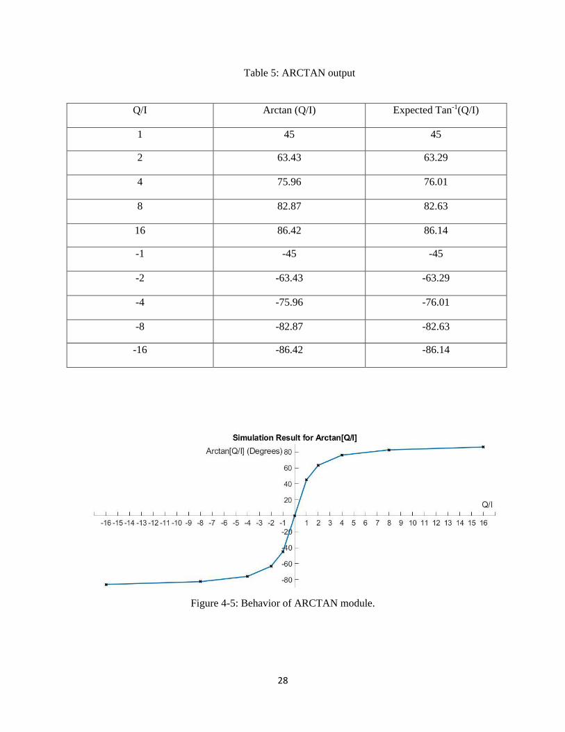
4.2.3 ARCTAN
The arctan function returns value in the range 𝝅
𝟐 𝒕𝒐
−𝝅
𝟐 and here, it is verified that the HDL
implemented arctan follows the same response. Table 5 presents the results obtained for the arctan
block for various Q/I values.
Figure 4-5 plots the results shown in table 5. It can be seen from Table 5 that the arctan block
produces results with considerable accuracy. Figure 4-5 verifies that the response of the implemented
arctan is as expected.
28
Table 5: ARCTAN output
Q/I Arctan (Q/I) Expected Tan-1(Q/I)
1 45 45
2 63.43 63.29
4 75.96 76.01
8 82.87 82.63
16 86.42 86.14
-1 -45 -45
-2 -63.43 -63.29
-4 -75.96 -76.01
-8 -82.87 -82.63
-16 -86.42 -86.14
Figure 4-5: Behavior of ARCTAN module.

29
4.2.4 Phase-Frequency Conversion
The phase-frequency conversion block is implemented using a simple difference equation
relating phase and frequency, as discussed in earlier section.
Figure 4-6: Phase-Frequency Relation.
As can be seen in the above figure, the frequency tracks the variation in the phase and the
slope of the phase represents the frequency.
4.2.5 Pulse Width Modulation
The functionality of the PWM block can be seen in Figure 4-6. 16 clock cycles of the
reference clock define a period of the PWM signal. The 4-bit input word decides the duty cycle of the
PWM signal.

30
Figure 4-7: PWM Output.
4.3 Demodulated FM Spectrum
Figure 4-7 shows the demodulated FM spectrum obtained for the proposed design. The figure
shows the 100KHz baseband spectrum for the 98.7MHz FM channel. As discussed earlier, the
broadcasted FM spectrum carries a lot of additional information aside from the audio, as can be seen
in Figure 4-7.
Figure 4-8: 100KHz Demodulated FM Spectrum.
However, the audio information is stored in the spectrum below 15KHz. For a mono audio
output, the spectrum up to 15KHz is relevant, as seen in figure 4-8.

31
Figure 4-9: Mono Audio Spectrum for Demodulated Channel.
4.4 Chapter Summary
In this chapter, each individual HDL block was designed and simulated using Verilog. The
design functionality has presented through Verilog testbenches. Simulation results verify the correct
functionality of every block. It is concluded that the proposed design demodulates the desired FM
channel and presents the entire 100KHz spectrum for the desired FM channel. The netlists for each
block was generated once the simulations were verified.
32
Chapter 5
Conclusion
The proposed work implements an all-digital FM demodulator for FPGA implementation.
The proposed design is a quadrature demodulator that extracts the phase information through I and Q
components and then converts it into frequency information. The design was able to deliver the
desired output spectrum.
To make the circuit compatible for high-speed needs, it was ensured that each block of the
design was implemented without using any multipliers. A CIC filter was used to carry out decimation
and low pass filtering, as compared to a more traditional FIR approach. This allows the filtering
operations to be executed using adders/subtractors. Also, the high-speed ADC enables the design to
have minimal analog frontend.
The design was implemented using Verilog HDL. The simulations were carried out in Icarus
Verilog and ModelSim, through Verilog testbenches. The netlists for the design are generated using
Vivado 2019.1.
5.1 Proposed Research and Contributions
Proposed research
◆ Design an all-digital FM demodulator using an FPGA.
Key contribution
◆ Design and verification of all digital FM demodulator through simulation
Key features
◆ Filtering, sinusoidal generation and phase detection are accomplished without
multipliers.
◆ Adopt PWM at the output to avoid a DAC.

33
5.2 Future Goals
The following additions and modifications can be made to the proposed to design for a better
implementation or even an increased functionality,
• Hardware Implementation: Once the JESD204B serial IP core becomes feasible, the
design can be directly implemented on to the FPGA and tested with high-speed
ADCs.
• Radio Data System (RDS) Information: The design can be extended to extract the
RDS information from the demodulated FM spectrum.
• NOAA weather radio: The high-speed high-bandwidth ADC capture a wide spectrum
of data. The design can be modified to capture other VHF standards.

34
Appendix
A. Block netlists
Figure A-1: CIC Decimator

35
.
FigureA-2: Sine/cosine generator
Figure A-3: ARCTAN.
36
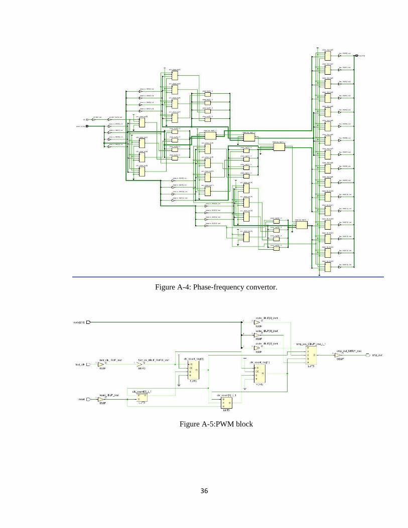
Figure A-4: Phase-frequency convertor.
Figure A-5:PWM block
37
References
[1] J. Bouloc, L. Nony, C. Loppacher, W. Rahajandraibe, F. Bocquet and L. Zaid, "FPGA-based
programmable digital PLL with very high frequency resolution," 2011 18th IEEE
International Conference on Electronics, Circuits, and Systems, Beirut, 2011, pp. 370-373.
[2] M. Kumm, H. Klingbeil and P. Zipf, "An FPGA-Based Linear All-Digital Phase-Locked
Loop," in IEEE Transactions on Circuits and Systems I: Regular Papers, vol. 57, no. 9, pp.
2487-2497, Sept. 2010.
[3] S. Edway and R. K. Manjunath, "Design and simulation of FPGA based all digital phase
locked loop (ADPLL)," 2017 3rd International Conference on Applied and Theoretical
Computing and Communication Technology (iCATccT), Tumkur, 2017, pp. 259-263.
[4] J. M. P. Langlois, D. Al-Khalili and R. J. Inkol, "A high performance, wide bandwidth, low
cost FPGA-based quadrature demodulator," Engineering Solutions for the Next Millennium.
1999 IEEE Canadian Conference on Electrical and Computer Engineering (Cat.
No.99TH8411), Edmonton, Alberta, Canada, 1999, pp. 497-502 vol.1
[5] S. Mankovskyy and E. Mankovska, "Symbolic model of the quadrature detector," 2016 13th
International Conference on Modern Problems of Radio Engineering, Telecommunications
and Computer Science (TCSET), Lviv, 2016, pp. 87-89.
[6] Y. Guo, J. Fu, B. Chi, Y. Wang and J. Cui, "Analysis and design of a 400MHz-6GHz
quadrature demodulator with high linearity," 2016 5th International Symposium on Next-
Generation Electronics (ISNE), Hsinchu, 2016, pp. 1-2
[7] Fubing Yi, "FPGA implementation of a fully digital FM demodulator," The Ninth
International Conference onCommunications Systems, 2004. ICCS 2004., Singapore, China,
2004, pp. 446-450
[8] Martos, Pedro Ignacio, and José Luis Bonadero. "FPGA-based digital demodulation." XII
Reunión de Trabajo en Procesamiento de la Información y Control 16 (2007).
[9] F. Schnyder and C.Haller, Implementation of FM Demodulator Algorithms on a High
Performance Digital Signal Processor, Nanyang Technological University and Hochschule
For Technik Rapperswil, 2002.
[10] G. J. Dolecek and S. K. Mitra, "Two-stage CIC-based decimator with improved
characteristics," in IET Signal Processing, vol. 4, no. 1, pp. 22-29, February 2010.
38
[11] D. Sinha and S. Kumar, "CIC filter for sample rate conversion in software defined radio,"
2016 World Conference on Futuristic Trends in Research and Innovation for Social Welfare
(Startup Conclave), Coimbatore, 2016, pp. 1-5
[12] R. Bhakthavatchalu, V. S. Karthika, L. Ramesh and B. Aamani, "Design of optimized CIC
decimator and interpolator in FPGA," 2013 International Mutli-Conference on Automation,
Computing, Communication, Control and Compressed Sensing (iMac4s), Kottayam, 2013,
pp. 812-817.
[13] V. Elamaran, R. Vaishnavi, A. M. Rozario, S. M. Joseph and A. Cherian, "CIC for
decimation and interpolation using Xilinx system generator," 2013 International Conference
on Communication and Signal Processing, Melmaruvathur, 2013, pp. 622-626.
[14] H. R. Gupta and R. Mehra, "Analysis & implementation of high cascaded integrated comb
for software defined radios application," 2015 Third International Conference on Image
Information Processing (ICIIP), Waknaghat, 2015, pp. 97-101.
[15] Du Weitao and Yang Zhanxin, "Design of area efficient DDS IP core generator," 2015 12th
IEEE International Conference on Electronic Measurement & Instruments (ICEMI),
Qingdao, 2015, pp. 443-446.
[16] X. Wang and Q. Mei, "High-Precision Design of DDS Based on FPGA," 2012 Third Global
Congress on Intelligent Systems, Wuhan, 2012, pp. 386-389.
[17] Zeliang Liu, "Design of typical waveform generator based on DDS/SOPC," Proceedings
2013 International Conference on Mechatronic Sciences, Electric Engineering and Computer
(MEC), Shengyang, 2013, pp. 642-645.
[18] Y. Fang and X. Chen, "Design and simulation of DDS based on Quartus II," 2011 IEEE
International Conference on Computer Science and Automation Engineering, Shanghai,
2011, pp. 357-360.
[19] J. Zhang and X. Li, "The Front Design and Implement of Direct Digital Frequency
Synthesizer Based on FPGA," 2010 International Conference on Electrical and Control
Engineering, Wuhan, 2010, pp. 4816-4819.
[20] Sithamparanathan Kandeepan, Omar Hashmi and Qian Zheng, "A complex-envelope based
digital phase locked loop with an arctan phase detector implemented on FPGA and
performance analysis," 2007 6th International Conference on Information, Communications
& Signal Processing, Singapore, 2007, pp. 1-5.

39
[21] N. Neji, A. Boudabous, W. Kharrat and N. Masmoudi, "Architecture and FPGA
implementation of the CORDIC algorithm for fingerprints recognition systems," Eighth
International Multi-Conference on Systems, Signals & Devices, Sousse, 2011, pp. 1-5.
[22] S. Aggarwal, P. K. Meher and K. Khare, "Concept, Design, and Implementation of
Reconfigurable CORDIC," in IEEE Transactions on Very Large Scale Integration (VLSI)
Systems, vol. 24, no. 4, pp. 1588-1592, April 2016.
[23] P. A. Kumar, "FPGA Implementation of the Trigonometric Functions Using the CORDIC
Algorithm," 2019 5th International Conference on Advanced Computing & Communication
Systems (ICACCS), Coimbatore, India, 2019, pp. 894-900.
[24] P. S. Wright and J. R. Pickering, "An AC voltage standard based on a PWM DAC," in IEEE
Transactions on Instrumentation and Measurement, vol. 48, no. 2, pp. 457-461, April 1999.
[25] S. Saponara, L. Fanucci and P. Terreni, "Oversampled and Noise-Shaped Pulse-Width
Modulator for High-Fidelity Digital Audio Amplifier," 2006 13th IEEE International
Conference on Electronics, Circuits and Systems, Nice, 2006, pp. 830-833.