al2o3 thin films deposited by thermal atomic layer …...al2o3 thin films deposited by thermal...
TRANSCRIPT
HAL Id: hal-01712453https://hal.archives-ouvertes.fr/hal-01712453
Submitted on 19 Feb 2018
HAL is a multi-disciplinary open accessarchive for the deposit and dissemination of sci-entific research documents, whether they are pub-lished or not. The documents may come fromteaching and research institutions in France orabroad, or from public or private research centers.
L’archive ouverte pluridisciplinaire HAL, estdestinée au dépôt et à la diffusion de documentsscientifiques de niveau recherche, publiés ou non,émanant des établissements d’enseignement et derecherche français ou étrangers, des laboratoirespublics ou privés.
Al2O3 thin films deposited by thermal atomic layerdeposition: Characterization for photovoltaic
applicationsCorina Barbos, Danièle Blanc-Pélissier, Alain Fave, Claude Botella, PhilippeRegreny, Geneviève Grenet, Elisabeth Blanquet, Alexandre Crisci, Mustapha
Lemiti
To cite this version:Corina Barbos, Danièle Blanc-Pélissier, Alain Fave, Claude Botella, Philippe Regreny, et al.. Al2O3thin films deposited by thermal atomic layer deposition: Characterization for photovoltaic applica-tions. Thin Solid Films, Elsevier, 2016, 617 (Part B), pp.108-113. �10.1016/j.tsf.2016.02.049�. �hal-01712453�
1
Al2O3 thin films deposited by thermal Atomic Layer Deposition: characterization for
photovoltaic applications
Corina Barbosa, Danièle Blanc-Pelissier
a*, Alain Fave
a, Elisabeth Blanquet
b,
Alexandre Criscib, Mustapha Lemiti
a
aUniversité de Lyon ; Institut des Nanotechnologies de Lyon INL - UMR5270, CNRS ; INSA Lyon ; Villeurbanne,
F-69621, France bScience et Ingénierie des Matériaux et Procédés (SIMaP), F-38 402, St Martin d’Heres, France
* Corresponding author at : Institut des Nanotechnologies de Lyon, INSA de Lyon, Bât Blaise Pascal, 7 avenue
Jean Capelle, 69621 Villeurbanne cedex
Tél : 33 (0)4 72 43 72 86
Fax : 33 (0)4 72 43 60 81
email : [email protected]
Keywords: Al2O3; Atomic layer deposition; Thin films; Interface characterization; Surface
passivation.
Abstract
Al2O3 thin films with thickness between 2 and 100 nm were synthetized at 250°C by thermal
atomic layer deposition on silicon substrates. Characterizations of as-deposited and annealed
layers were carried out using ellipsometry, X-ray reflectivity and X-ray photoelectron
spectroscopy. A silicon-rich SiOx layer at the interface between Si and Al2O3 was introduced
in the optical models to fit the experimental data. Surface passivation performances of Al2O3
layers deposited on n-type float-zone monocrystalline silicon were investigated as a function
of thickness and post-deposition annealing conditions. Surface recombination velocity around
2 cm.s-1
was measured after the activation of the negative charges at the Si/ Al2O3 interface
under optimized annealing at 400°C for 10 min. The evolution of the interface layer and of
the material properties with the thermal treatment was studied.
1. Introduction
Passivation of silicon surfaces is essential to achieve high solar cell performances. Several
trends in photovoltaics have played an important role in the popularity of Al2O3 for efficient
surface passivation. Firstly, the photovoltaic (PV) industry has been looking to improve the
rear side of conventional screen printed p-type Si solar cells by replacing the standard Al-back
surface field (BSF) by a dielectric-passivated rear side with localized BSF. Secondly, the use
of n-type Si which does not suffer from light induced degradation and is less sensitive to
common metal impurities, has become an attractive option for the fabrication of high solar
cell efficiencies. The high density of negative charges in Al2O3 is well suited for the
passivation of p+ emitters on n-type substrate [1]. A very high conversion efficiency of 23.9%
for an n-type Passivated Emitter Rear Locally Diffused PERL solar cell with a front side B-
doped emitter and an Al2O3 passivation layer has been reported [2,3]. Recent works [4, 5]
2
have demonstrated that Al2O3 could also be efficient for passivation of n-type silicon
substrates.
Along with Al2O3, atomic layer deposition (ALD) was introduced in the field of Si PV. ALD
differs from conventional (plasma enhanced) chemical vapor deposition methods by strict
separation of precursors in the reaction chamber. As the precursors can only react with the
wafer surface in a self-limiting way, film growth proceeds layer-by-layer and a very precise
thickness control is possible. This technique is ideal for depositing high quality, uniform and
conformal thin films at relatively low temperatures (100-250 °C). The passivation of high
aspect ratio surface texturation (nanowires, “black silicon”), used to improve the optical
confinement in advanced solar cells, requires a very conformal thin passivation layer. Al2O3
deposited by thermal ALD (more conformal than plasma enhanced ALD) becomes the ideal
candidate for this passivation layers.
Given the multiple advantages of Al2O3 deposited by ALD, this material has become widely
used for photovoltaic applications [6] where the commonly used thickness is less than 15 nm.
Therefore, an important need in very thin film characterization has appeared. However, very
thin films ( 10 nm) are difficult to characterize precisely as interfaces play a major role in the
data analysis. For example, thickness and refractive index are difficult to measure separately
by optical techniques like ellipsometry as they are highly correlated [7]. Consequently various
characterizations techniques and optical models should be used and compared in order to
determine very thin film properties.
In this study, Al2O3 layers with thicknesses in the range 2 to 100 nm were deposited by
thermal-ALD on n-type crystalline Si substrates. Fast, non-destructive and accurate
characterization techniques were chosen to analyze the Al2O3 layers and the interfaces.
Optical and geometrical properties of the Al2O3 layers were studied by ellipsometry and X-ray
reflectivity (XRR). Stoichiometry was measured by X-ray photoelectron spectroscopy (XPS)
to analyze the material and the interface structure. The surface passivation of the Si wafers
was evaluated by photo-conductance measurements. Characterization of the Al2O3 layers and
of the interfaces was performed before and after the thermal treatment that is required to
improve the surface passivation of silicon.
2. Sample preparation
We used 250 µm thick float zone (FZ) n-type double sided polished Si (100) substrates with a
resistivity of 10 Ω.cm. Sapphire substrates A-Plane (11-20) polished on the front side were
also used for additional ellipsometry measurements. Prior to deposition, the wafers were
cleaned using standard chemical process (Piranha [H2O2, H2SO4] and diluted HF). Al2O3
films were deposited by ALD in an Ultratech Fiji F200 reactor. Trimethylaluminium (Al
(CH3)3) and water (H2O) were used as reactants. The chuck and chamber temperature was set
to 250°C during deposition. Substrates were positioned on quartz holders to coat both surfaces
in the same run. This was particularly interesting for minority carrier lifetime measurements
that required passivation on both surfaces. For the present study the number of cycles was
3
varied between 20 and 1000, leading to film thicknesses between 2 and 100 nm. More
precisely, we measured previously a growth per cycle (GPC) of 0.098 nm per cycle at 250°C
on Si substrates [8]. After as-deposited characterizations, the samples were annealed in the
ALD chamber in direct contact with the chuck. A range of temperatures (350-450°C) and
annealing times (5-15 min) were applied. The argon pressure was kept at around 670 Pa. The
annealing step is essential for photovoltaic applications to activate the surface charges and
improve the surface passivation.
3. Results and discussion
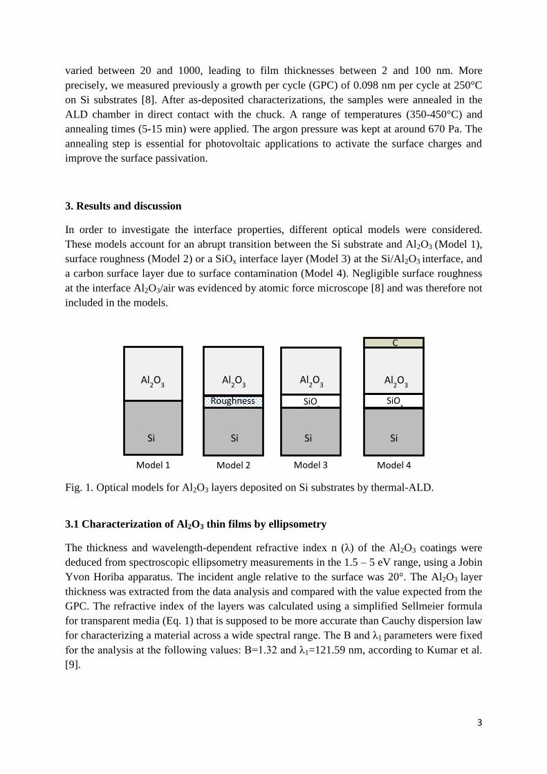
In order to investigate the interface properties, different optical models were considered.
These models account for an abrupt transition between the Si substrate and Al2O3 (Model 1),
surface roughness (Model 2) or a SiOx interface layer (Model 3) at the Si/Al2O3 interface, and
a carbon surface layer due to surface contamination (Model 4). Negligible surface roughness
at the interface Al2O3/air was evidenced by atomic force microscope [8] and was therefore not
included in the models.
Fig. 1. Optical models for Al2O3 layers deposited on Si substrates by thermal-ALD.
3.1 Characterization of Al2O3 thin films by ellipsometry
The thickness and wavelength-dependent refractive index n (λ) of the Al2O3 coatings were
deduced from spectroscopic ellipsometry measurements in the 1.5 – 5 eV range, using a Jobin
Yvon Horiba apparatus. The incident angle relative to the surface was 20°. The Al2O3 layer
thickness was extracted from the data analysis and compared with the value expected from the
GPC. The refractive index of the layers was calculated using a simplified Sellmeier formula
for transparent media (Eq. 1) that is supposed to be more accurate than Cauchy dispersion law
for characterizing a material across a wide spectral range. The B and λ1 parameters were fixed
for the analysis at the following values: B=1.32 and λ1=121.59 nm, according to Kumar et al.
[9].
Model 1
Al2O
3
Si
Model 3
Al2O
3
Si
SiOx
Model 4
Si
C
Model 2
Si
Al2O
3
Roughness
Al2O
3
SiOx
4
Eq.1
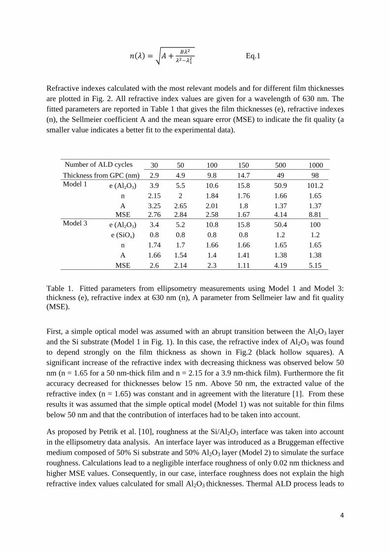
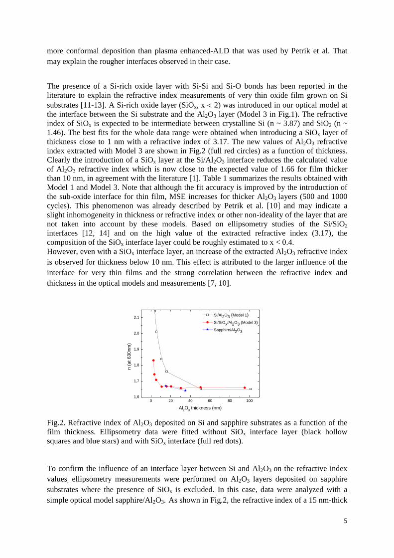
Refractive indexes calculated with the most relevant models and for different film thicknesses
are plotted in Fig. 2. All refractive index values are given for a wavelength of 630 nm. The
fitted parameters are reported in Table 1 that gives the film thicknesses (e), refractive indexes
(n), the Sellmeier coefficient A and the mean square error (MSE) to indicate the fit quality (a
smaller value indicates a better fit to the experimental data).
Number of ALD cycles 30 50 100 150 500 1000
Thickness from GPC (nm) 2.9 4.9 9.8 14.7 49 98
Model 1 e (Al2O3) 3.9 5.5 10.6 15.8 50.9 101.2
n 2.15 2 1.84 1.76 1.66 1.65
A 3.25 2.65 2.01 1.8 1.37 1.37
MSE 2.76 2.84 2.58 1.67 4.14 8.81
Model 3 e (Al2O3) 3.4 5.2 10.8 15.8 50.4 100
e (SiOx) 0.8 0.8 0.8 0.8 1.2 1.2
n 1.74 1.7 1.66 1.66 1.65 1.65
A 1.66 1.54 1.4 1.41 1.38 1.38
MSE 2.6 2.14 2.3 1.11 4.19 5.15
Table 1. Fitted parameters from ellipsometry measurements using Model 1 and Model 3:
thickness (e), refractive index at 630 nm (n), A parameter from Sellmeier law and fit quality
(MSE).
First, a simple optical model was assumed with an abrupt transition between the Al2O3 layer
and the Si substrate (Model 1 in Fig. 1). In this case, the refractive index of Al2O3 was found
to depend strongly on the film thickness as shown in Fig.2 (black hollow squares). A
significant increase of the refractive index with decreasing thickness was observed below 50
nm (n = 1.65 for a 50 nm-thick film and n = 2.15 for a 3.9 nm-thick film). Furthermore the fit
accuracy decreased for thicknesses below 15 nm. Above 50 nm, the extracted value of the
refractive index (n = 1.65) was constant and in agreement with the literature [1]. From these
results it was assumed that the simple optical model (Model 1) was not suitable for thin films
below 50 nm and that the contribution of interfaces had to be taken into account.
As proposed by Petrik et al. [10], roughness at the Si/Al2O3 interface was taken into account
in the ellipsometry data analysis. An interface layer was introduced as a Bruggeman effective
medium composed of 50% Si substrate and 50% Al2O3 layer (Model 2) to simulate the surface
roughness. Calculations lead to a negligible interface roughness of only 0.02 nm thickness and
higher MSE values. Consequently, in our case, interface roughness does not explain the high
refractive index values calculated for small Al2O3 thicknesses. Thermal ALD process leads to
5
more conformal deposition than plasma enhanced-ALD that was used by Petrik et al. That
may explain the rougher interfaces observed in their case.
The presence of a Si-rich oxide layer with Si-Si and Si-O bonds has been reported in the
literature to explain the refractive index measurements of very thin oxide film grown on Si
substrates [11-13]. A Si-rich oxide layer (SiOx, x 2) was introduced in our optical model at
the interface between the Si substrate and the Al2O3 layer (Model 3 in Fig.1). The refractive
index of SiOx is expected to be intermediate between crystalline Si (n ~ 3.87) and SiO2 (n ~
1.46). The best fits for the whole data range were obtained when introducing a SiOx layer of
thickness close to 1 nm with a refractive index of 3.17. The new values of Al2O3 refractive
index extracted with Model 3 are shown in Fig.2 (full red circles) as a function of thickness.
Clearly the introduction of a SiOx layer at the Si/Al2O3 interface reduces the calculated value
of Al2O3 refractive index which is now close to the expected value of 1.66 for film thicker
than 10 nm, in agreement with the literature [1]. Table 1 summarizes the results obtained with
Model 1 and Model 3. Note that although the fit accuracy is improved by the introduction of
the sub-oxide interface for thin film, MSE increases for thicker Al2O3 layers (500 and 1000
cycles). This phenomenon was already described by Petrik et al. [10] and may indicate a
slight inhomogeneity in thickness or refractive index or other non-ideality of the layer that are
not taken into account by these models. Based on ellipsometry studies of the Si/SiO2
interfaces [12, 14] and on the high value of the extracted refractive index (3.17), the
composition of the SiOx interface layer could be roughly estimated to x < 0.4.
However, even with a SiOx interface layer, an increase of the extracted Al2O3 refractive index
is observed for thickness below 10 nm. This effect is attributed to the larger influence of the
interface for very thin films and the strong correlation between the refractive index and
thickness in the optical models and measurements [7, 10].
0 20 40 60 80 1001,6
1,7
1,8
1,9
2,0
2,1
n (
at 6
30
nm
)
Al2O
3 thickness (nm)
Si/Al2O3 (Model 1)
Si/SiOx/Al2O3 (Model 3)
Sapphire/Al2O3
Fig.2. Refractive index of Al2O3 deposited on Si and sapphire substrates as a function of the
film thickness. Ellipsometry data were fitted without SiOx interface layer (black hollow
squares and blue stars) and with SiOx interface (full red dots).
To confirm the influence of an interface layer between Si and Al2O3 on the refractive index
values, ellipsometry measurements were performed on Al2O3 layers deposited on sapphire
substrates where the presence of SiOx is excluded. In this case, data were analyzed with a
simple optical model sapphire/Al2O3. As shown in Fig.2, the refractive index of a 15 nm-thick
6
Al2O3 was 1.67. This result is in very good agreement with results obtained using Model 3 and
tends to confirm the existence of the SiOx interface layer at the interface Si/Al2O3.
A final hypothesis, taking into account both a SiOx interface layer and a possible surface
hydro-carbon contamination (Model 4) was also investigated. The calculated thickness of the
C-layer was close to zero (0.001 nm). Therefore, surface contamination does not have a
significant influence on ellipsometry measurements.
In summary, our ellipsometry results do not seem compatible with an abrupt transition
between the Si substrate and Al2O3 or with interface roughness. The best-fit model of
ellipsometry data was obtained with a SiOx layer at the Si/Al2O3 interface of thickness around
1nm and refractive index around 3.17 at 630 nm. This buried oxide layer is probably
introduced via cleaning prior to deposition as HF etching leads to a Si-O-H surface which can
be transformed into SiOx during the very first stages of the ALD process [10].
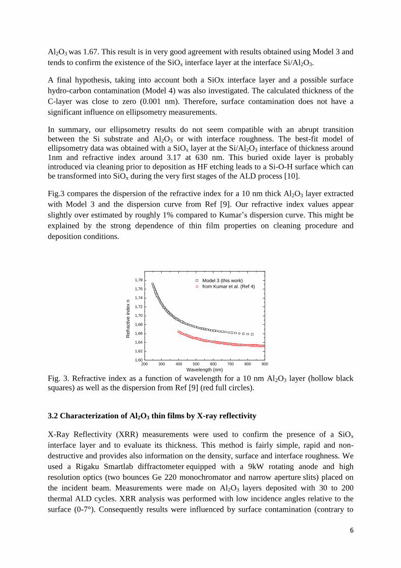
Fig.3 compares the dispersion of the refractive index for a 10 nm thick Al2O3 layer extracted
with Model 3 and the dispersion curve from Ref [9]. Our refractive index values appear
slightly over estimated by roughly 1% compared to Kumar’s dispersion curve. This might be
explained by the strong dependence of thin film properties on cleaning procedure and
deposition conditions.
200 300 400 500 600 700 800 900
1,60
1,62
1,64
1,66
1,68
1,70
1,72
1,74
1,76
1,78
Wavelength (nm)
Re
fra
ctive in
de
x n
Model 3 (this work)
from Kumar et al. (Ref 4)
Fig. 3. Refractive index as a function of wavelength for a 10 nm Al2O3 layer (hollow black
squares) as well as the dispersion from Ref [9] (red full circles).
3.2 Characterization of Al2O3 thin films by X-ray reflectivity
X-Ray Reflectivity (XRR) measurements were used to confirm the presence of a SiOx
interface layer and to evaluate its thickness. This method is fairly simple, rapid and non-
destructive and provides also information on the density, surface and interface roughness. We
used a Rigaku Smartlab diffractometer equipped with a 9kW rotating anode and high
resolution optics (two bounces Ge 220 monochromator and narrow aperture slits) placed on
the incident beam. Measurements were made on Al2O3 layers deposited with 30 to 200
thermal ALD cycles. XRR analysis was performed with low incidence angles relative to the
surface (0-7°). Consequently results were influenced by surface contamination (contrary to

7
0 1 2 3
102
103
104
105
106
107
Experimental
Model 4 (Si/SiOx/Al
2O
3/C)
Model 3 (Si/SiOx/Al
2O
3)
XR
Inte
nsity (
a.u
.)
2Theta (°)
the ellipsometry, where a 20° angle relative to the surface was used). For this reason data
were also analyzed with a model that takes into account a carbon surface layer in Fig.1.
Examples of measurements performed on very thin films (30 to 100 cycles) are shown in Fig.
4. The reflectivity profile showed oscillations caused by interference between the X-rays
reflected at the different interfaces. Since these oscillations were used to calculate the
thickness of the layers, it appeared that the minimum measurable film thickness was about 3
nm for Al2O3 on Si, when oscillations are still visible. Model 3 (Si/SiOx/Al2O3) was used to fit
the data in Fig.4.
Fig. 4. XRR data (black) and fitted curve (red) for different Al2O3 thicknesses.
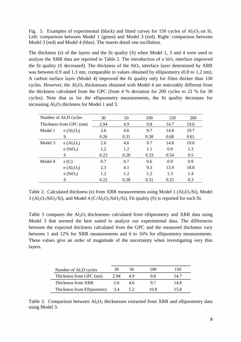
Data analyses using the different models introduced for ellipsometry were compared. Fig. 5
shows on an enlarged scale the theoretical and fitted curves obtained with Model 1, 3 and 4
for a 150 cycles film. It is quite clear from Fig.5 (left) that Model 3 (SiOx interface) lead to a
closer fit than Model 1 (abrupt Si/Al2O3). On the other hand, the introduction of a C-layer at
the interface Si/air (Model 4) did not provide a significant improvement on the fitting
accuracy as compared to Model 3 (Fig.5 right).
0 1 2 3
102
103
104
105
106
107
Experimental
Model 3 (Si/SiOx/Al
2O
3)
Model 1 (Si/Al2O
3)
XR
Inte
nsity (
a.u
.)
2Theta (°)
0 1 2 3 4 5 6 7 8
100
102
104
106
0 1 2 3 4 5 6 7 8
100
102
104
106
0 1 2 3 4 5 6 7 8
102
104
106
3 nm
XR
R in
ten
sity (
a.u
.)
5 nm
2 Theta (°)
10 nm
1,4 1,6 1,8
103
104
2 Theta (°)
XR
inte
nsity (
a.u
.)
1,4 1,6 1,8
103
104
XR
in
ten
sity (
a.u
.)
2 Theta (a.u.)
8
Fig. 5. Examples of experimental (black) and fitted curves for 150 cycles of Al2O3 on Si.
Left: comparison between Model 1 (green) and Model 3 (red). Right: comparison between
Model 3 (red) and Model 4 (blue). The inserts detail one oscillation.
The thickness (e) of the layers and the fit quality (S) when Model 1, 3 and 4 were used to
analyze the XRR data are reported in Table 2. The introduction of a SiOx interface improved
the fit quality (S decreased). The thickness of the SiOx interface layer determined by XRR
was between 0.9 and 1.3 nm, comparable to values obtained by ellipsometry (0.8 to 1.2 nm).
A carbon surface layer (Model 4) improved the fit quality only for films thicker than 150
cycles. However, the Al2O3 thicknesses obtained with Model 4 are noticeably different from
the thickness calculated from the GPC (from 4 % deviation for 200 cycles to 21 % for 30
cycles). Note that as for the ellipsometry measurements, the fit quality decreases for
increasing Al2O3 thickness for Model 1 and 3.
Table 2. Calculated thickness (e) from XRR measurements using Model 1 (Al2O3/Si), Model
3 (Al2O3/SiO2/Si), and Model 4 (C/Al2O3/SiO2/Si). Fit quality (S) is reported for each fit.
Table 3 compares the Al2O3 thicknesses calculated from ellipsometry and XRR data using
Model 3 that seemed the best suited to analyze our experimental data. The differences
between the expected thickness calculated from the GPC and the measured thickness vary
between 1 and 12% for XRR measurements and 6 to 16% for ellipsometry measurements.
These values give an order of magnitude of the uncertainty when investigating very thin
layers.
Number of ALD cycles 30 50 100 150
Thickness from GPC (nm) 2.94 4.9 9.8 14.7
Thickness from XRR 2.6 4.6 9.7 14.8
Thickness from Ellipsometry 3.4 5.2 10.8 15.8
Table 3. Comparison between Al2O3 thicknesses extracted from XRR and ellipsometry data
using Model 3.
Number of ALD cycles 30 50 100 150 200
Thickness from GPC (nm) 2.94 4.9 9.8 14.7 19.6
Model 1 e (Al2O3) 2.6 4.6 9.7 14.8 19.7
S 0.26 0.31 0.38 0.68 0.61
Model 3 e (Al2O3) 2.6 4.6 9.7 14.8 19.6
e (SiOx) 1.2 1.2 1.1 0.9 1.3
S 0.23 0.28 0.33 0.54 0.5
Model 4 e (C) 0.7 0.7 0.6 0.9 0.9
e (Al2O3) 2.3 4.1 9.3 13.9 18.8
e (SiOx) 1.2 1.2 1.2 1.3 1.4
S 0.22 0.28 0.31 0.25 0.3
9
The density of the SiOx interface layer given by XRR data analysis was 2.29 g.cm-3
. As the
density of SiO2 and Si are 2.2 g.cm-3
and 2.33 g.cm-3
respectively, x can be estimated to be
<0.5 assuming a linear variation of the density with composition. This value is in agreement
with our previous estimation of x < 0.4 obtained by ellipsometry. From XRR data, the
calculated density of the Al2O3 layer deposited at 250°C was 3.2 g/cm3. This value is in
agreement with the density of 3.15 g/cm3 reported by Triani [15] for a deposition temperature
of 200°C. Indeed, the density of ALD films decreases at lower deposition temperatures as
noted by Groner [16], who reported a density of 3 g/cm3 for a deposition temperature of
177°C. More generally, the densities of thin Al2O3 films deposited by ALD are significantly
smaller than the reported values of 3.75-3.95 g/cm3
for bulk alumina [17].
3.3 Chemical composition of Al2O3 thin films
Chemical composition was measured by X-Ray Photoelectron Spectroscopy (XPS) and by
Electron Probe Micro-Analysis (EPMA) on as-deposited Al2O3 layers of different thicknesses
to investigate the material composition and the interface structure. XPS measurements were
carried out in a Vacuum Science Workshop chamber equipped with a monochromatic X-ray
source Al K-alpha (1486.6eV). The angle between the X-ray source and the photoelectron
detector was 54.7°. EPMA was performed with a CAMECA SX50 equipped with four
vertical wavelength dispersive spectrometers.
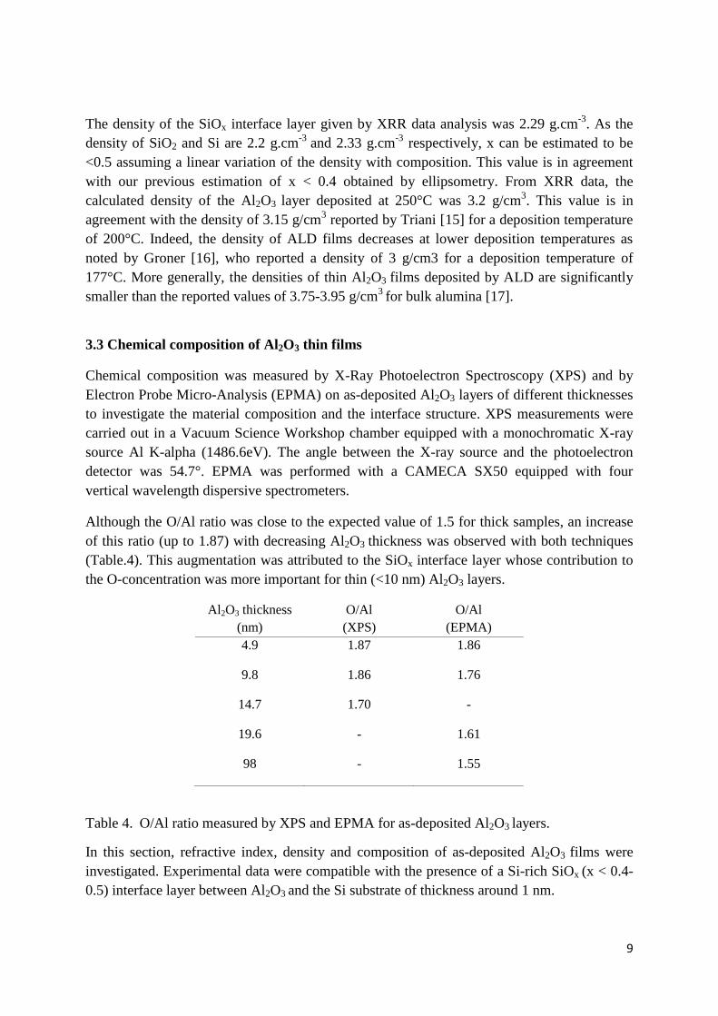
Although the O/Al ratio was close to the expected value of 1.5 for thick samples, an increase
of this ratio (up to 1.87) with decreasing Al2O3 thickness was observed with both techniques
(Table.4). This augmentation was attributed to the SiOx interface layer whose contribution to
the O-concentration was more important for thin (<10 nm) Al2O3 layers.
Al2O3 thickness
(nm)
O/Al
(XPS)
O/Al
(EPMA)
4.9 1.87 1.86
9.8 1.86 1.76
14.7 1.70 -
19.6 - 1.61
98 - 1.55
Table 4. O/Al ratio measured by XPS and EPMA for as-deposited Al2O3 layers.
In this section, refractive index, density and composition of as-deposited Al2O3 films were
investigated. Experimental data were compatible with the presence of a Si-rich SiOx (x < 0.4-
0.5) interface layer between Al2O3 and the Si substrate of thickness around 1 nm.
10
3.4 Effect of thermal annealing on the properties of the Al2O3 thin films
The application of the Al2O3 layers to surface passivation of Si solar cells requires further
processing and characterization. As-deposited Al2O3 layers grown by thermal-ALD provide
already a significant level of surface passivation of Si substrates mainly due to the reduction
of the electrically active interface states (dangling bonds) by chemical bonding. However,
further reduction of the surface recombination requires the activation of charges at the
Al2O3/Si interface that provide a field-effect passivation. Negative charges are activated by
thermal annealing. This section describes the optimization of the annealing process, the
surface recombination velocity measurements and the effect of the thermal treatment on the
material and interfaces parameters discussed in section 3.1 to 3.3.
The impact of surface recombination on solar cell efficiency can be evaluated by measuring
the minority carrier lifetime (τeff). The effective lifetime can be expressed as a bulk lifetime
(bulk) and a surface lifetime (surface) contribution [18]:
surfacebulkeff
111 (1)
For a symmetrically passivated wafer with sufficiently low surface defect density, Eq. 1 can
be expressed as:
e
S
bulkeff
211
(2)
S is the surface recombination velocity and e is the wafer thickness [18]. For the high
resistivity Si substrates used in this study with bulk lifetimes larger than10 ms, S can be
directly related to τeff by S = e/2 τeff.
The minority carrier lifetime was evaluated by Photo-Conductance Decay using a Sinton
Instruments WCT-120 system [19]. This parameter was first measured on as-deposited n-type
Si substrates coated on both sides with Al2O3 layers of various thicknesses (from 5 to 50 nm).
The surface passivation increased for Al2O3 layers between 5 and 15 nm and tended to
stabilize for larger thicknesses. For an injection level of 2.1014
cm-3
, τeff was 1.2 ms for 5 nm
of Al2O3 and 2 ms for 15 nm. The augmentation of τeff for as-deposited thicker films was
related to the deposition time and attributed to an in situ annealing effect taking place in the
ALD reactor during deposition at 250°C [1].
After τeff measurements on as-deposited samples, annealing was done on the samples coated
with 15 nm of Al2O3. The Ar pressure was kept constant to 670 Pa. Temperature was varied
between 350°C and 450°C and annealing time was varied between 5 min and 15 min. As
reported previously, maximum τeff values around 5.8 ms were measured after annealing at
400°C for 10 min [8]. From the maximum τeff value of 5.8 ms, the surface recombination
velocity was estimated to S around 2.4 cm/s. This result is in good agreement with the very
low surface recombination velocities S <5 cm/s reported in the literature [1].
11
Once the annealing step was optimized in order to obtain the lowest surface recombination
velocity, the effect of the thermal treatment (400°C for 10 min) on the material and interfaces
parameters determined in the previous section was evaluated by ellipsometry, XRR and XPS
measurements. Ellipsometry measurements after the annealing step revealed a slight increase
(less than 3 %) of the refractive index with the assumption that the thickness of Al2O3 did not
change with temperature. This could indicate an increase of density of Al2O3 after thermal
treatment. From XRR measurements the density of alumina layers was found to increase by
4% after annealing, rising from 3.2 g/cm3
to 3.33 g/cm3 in agreement with XRR observation.
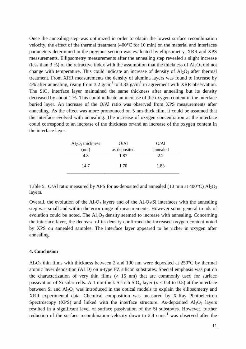
The SiOx interface layer maintained the same thickness after annealing but its density
decreased by about 1 %. This could indicate an increase of the oxygen content in the interface
buried layer. An increase of the O/Al ratio was observed from XPS measurements after
annealing. As the effect was more pronounced on 5 nm-thick film, it could be assumed that
the interface evolved with annealing. The increase of oxygen concentration at the interface
could correspond to an increase of the thickness or/and an increase of the oxygen content in
the interface layer.
Al2O3 thickness
(nm)
O/Al
as-deposited
O/Al
annealed
4.8 1.87 2.2
14.7 1.70 1.83
Table 5. O/Al ratio measured by XPS for as-deposited and annealed (10 min at 400°C) Al2O3
layers.
Overall, the evolution of the Al2O3 layers and of the Al2O3/Si interfaces with the annealing
step was small and within the error range of measurements. However some general trends of
evolution could be noted. The Al2O3 density seemed to increase with annealing. Concerning
the interface layer, the decrease of its density confirmed the increased oxygen content noted
by XPS on annealed samples. The interface layer appeared to be richer in oxygen after
annealing.
4. Conclusion
Al2O3 thin films with thickness between 2 and 100 nm were deposited at 250°C by thermal
atomic layer deposition (ALD) on n-type FZ silicon substrates. Special emphasis was put on
the characterization of very thin films ( 15 nm) that are commonly used for surface
passivation of Si solar cells. A 1 nm-thick Si-rich SiOx layer (x < 0.4 to 0.5) at the interface
between Si and Al2O3 was introduced in the optical models to explain the ellipsometry and
XRR experimental data. Chemical composition was measured by X-Ray Photoelectron
Spectroscopy (XPS) and linked with the interface structure. As-deposited Al2O3 layers
resulted in a significant level of surface passivation of the Si substrates. However, further
reduction of the surface recombination velocity down to 2.4 cm.s-1
was observed after the
12
activation of the negative charges at the Si/ Al2O3 interface under optimized annealing
conditions (400°C for 10 min). The stability of the Al2O3 layer after annealing was confirmed
by ellipsometry, XRR and XPS although the Al2O3 density increased slightly and the SiOx
interface layer appeared to be richer in oxygen after annealing.
Acknowledgements
Corina Barbos is grateful to Région Rhône-Alpes (ARC-4 Energies) for a supporting grant.
References
[1] G. Dingemans, W.M. M. Kessels, Status and prospects of Al2O3-based surface passivation schemes
for silicon solar cells, J. Vac. Sci. Technol. A30 (2012) 040802-1.
[2] S. W. Glunz, J. Benick, D. Biro, M. Bivour, M. Hermle, D. Pysch, M. Rauer. C. Reichel, A.
Richter, M. Rudiger, C. Schmiga, D. Suwito, A. Wolf, R. Preu, n-Type Silicon- enabling
efficiencies>20% in industrial production, 35th IEEE Conf. Proc. (2010) 50-56.
[3] J. Benick, B. Hoex, M.C.M. van de Sanden, W.M.M. Kessels, O. Schultz, S.W. Glunz, High
efficiency n-type Si solar cells on Al2O3-passivated boron emitters, Appl. Phys. Lett. 92 (2008)
253504-1.
[4] P. Repo, H. Talvitie, S. Li, J. Skarp, H. Savin, Silicon surface passivation by Al2O3: effect of ALD
reactants, Energy Procedia 8 (2011) 681-687.
[5] B. Hoex, J. Shmidt, P. Pohl, M.C.M. van de Sanden, W.M.M Kessels, Silicon surface passivation
by atomic layer deposited Al2O3, J. Appl. Phys. 104 (2008) 044903.
[6] International Technology Roadmap for Photovoltaics 2014 Results, 6th ed. (2015).
[7] D. Chandler-Horowitz, N.V. Nguyen, J.R. Ehrstein, Assessment of ultra-thin SiO2 film thickness
measurement precision by ellipsometry, AIP Conf. Proc. 683 (2003) 326-330.
[8] C. Barbos, D. Blanc-Pelissier, A. Fave, E. Blanquet, A. Crisci, E. Fourmond, D. Albertini, A.
Sabac, K. Ayadi, M. Lemiti, Characterization of Al2O3 thin films prepared by ALD, Accepted for
publication in Energy Proceedia, 77 (2015) 558-564.
[9] P. Kumar, M.K. Wiedmann, C.H. Winter and I. Avrutsky, Optical properties of Al2O3 thin films
grown by atomic layer deposition, Appl Opt. (2009) 5407-12.
[10] P. Petrik, T. Gumprecht , A. Nutsch , G. Roeder , M. Lemberger , G. Juhasz , O. Polgar , C.
Major , P. Kozma , M. Janosov, B. Fodor, E. Agocs, M. Fried, Comparative measurements on atomic
layer deposited Al2O3 thin films using ex situ table top and mapping ellipsometry, as well as X-ray and
VUV reflectometry, Thin Solid Films 541 (2013) 131-135.
[11] H. Fujiwara, Spectroscopic ellipsometry: principles and applications, Wiley, West Sussex, U.K.
2007.
[12] D.E. Aspnes, J.B. Theeten, Optical properties of the interface between Si and its thermally grown
oxide, Phys. Rev. Lett. 43 (1979) 1046–1050.
[13] E. Langereis, S.B.S. Heil, H.C.M. Knoops, W. Keuning, M.C.M. van de Sanden, W.M.M.
Kessels, In situ spectroscopic ellipsometry as a versatile tool for studying atomic layer deposition, J.
Appl. Phys. 42 (2009) 073001.
[14] N. Tomozeiu, Silicon Oxide (SiOx, 0<x<2): a Challenging Material for Optoelectronics, in: P.
Predeep (Ed.), Optoelectronics- Materials and techniques, InTech, 2011, pp. 55-98.
[15] G. Triani, P.J. Evans, D.R.G. Mitchell, D.J. Attard, K.S. Finnie, M. James, T. Hanley, B. Latella,
K.E. Prince, J. Bartlett, Atomic layer deposition of TiO2/Al2O3 films for optical applications, in:
Advances in Thin-Film Coatings for Optical Applications II, edited by Michael L. Fulton, Jennifer D.
T. Kruschwitz, Proc. of SPIE Vol. 5870 (2005) 587009.
[16] M.D. Groner, F.H. Fabreguette, J.W. Elam, S.M.George, Low-temperature Al2O3 Atomic Layer
Deposition, Chem. Mater. 16 (2004) 639-645.
13
[17] D.R. Lide, CRC Handbook of Chemistry and Physics, 75th ed., CRC Press, Boca Raton, 1994.
[18] A.B. Sproul, Dimensionless solution of the equation describing the effect of surface
recombination on carrier decay in semiconductors, J. Appl. Phys. 76 (1994) 2851-2854.
[19] R. A. Sinton, A. Cuevas, M. Stuckings, Quasi-steady-state photoconductance, a new method for
solar cell material and device characterization, 25th IEEE Conf. Proc. (1996) 457-460.