films deposited from reactive sputtering of aluminum
TRANSCRIPT
DOI: http://dx.doi.org/10.1590/1980-5373-MR-2016-0647Materials Research. 2017; 20(4): 926-936 © 2017
Films Deposited from Reactive Sputtering of Aluminum Acetylacetonate Under Low Energy Ion Bombardment
Felipe Augusto Darriba Battaglina, Eduardo Silva Pradoa, Luciano Caselib, Tiago Fiorini da Silvac,
Manfredo Harri Tabacniksc, Nilson Cristino da Cruza, Elidiane Cipriano Rangela*
Received: September 08, 2016; Revised: February 21, 2017; Accepted: March 10, 2017
Films were deposited from aluminum acetylacetonate (Al(acac)3) using a methodology involving reactive sputtering and low energy ion bombardment. The plasma was generated by the application of radiofrequency power to the powder containing electrode and simultaneously, negative pulses were supplied to the electrode where the substrates were attached. It was investigated the effect of the duty cycle of the pulses (Δ) on the properties of the coatings. Association of ion bombardment to the deposition process increased film thickness, structure reticulation and organic content. Ions from the deposition environment were implanted at the film-air interface or underneath it. Morphology and topography were altered depending on Δ. Considering the enhancement of Δ, it affected the flux of ions reaching the depositing interface and then the deposition rate, H content, crosslinking degree and surface microstructure. Alumina groups were detected in the infrared spectra, whereas the precipitation of amorphous alumina was confirmed by X-ray diffraction.
Keywords: Ion bombardment, Aluminum acetylacetonate, Duty cycle
* e-mail: [email protected]
1. Introduction
Alumina coatings (Al2O3) are attractive materials since they possess high electrical resistivity, hardness, wear and corrosion resistance, besides being good thermal insulators, chemically inert and physically stable at high temperatures1,2. As a consequence, alumina presents a branched field of applications as dielectric materials in microelectronic devices, barriers against corrosion, passivation layers, hardening coatings, abrasives, amongst others3-6.
Alumina can exist in the amorphous and crystalline phases, being the last category subdivided in metastable phases, called transition aluminas, and a single stable phase that is called alpha alumina (α)3. Each phase of alumina can be used in a specific application; however the one of greatest interest is the alpha stable phase, once it grants alumina its well-known advantages7.
The most used technique for alumina films synthesis is the chemical vapor deposition, CVD, which requires temperatures above 1000°C1-2, 8. Owing to this high temperature range, the versatility of the method is limited since some metallic and polymeric materials cannot be coated5. Moreover, the precursors normally used in the deposition process, dimethylaluminum isopropoxide (DMAI)3, trimethylaluminum (TMA)9 and
aluminum trichloride7, present the drawback of generating corrosive by-products, being expensive and difficult to handle6.
In the attempt to suppress these limitations, many studies are being developed based on techniques that involve plasma, as the PECVD, since the plasma supplies energy without the need of heating. With regard to the precursors, the use of aluminum acetylacetonate has increased (Al(acac)3), because this organometallic compound is cheap, easy to handle and does not generate harmful by-products10.
Zhao and Suhr6 deposited aluminum oxide films by Plasma Enhanced Chemical Vapor Deposition, PECVD, using aluminum acetylacetonate as precursor, which was decomposed in a heated cell (150-170˚C) and carried to the deposition chamber. Despite the heating of the sample holder (300 to 500˚C), amorphous films were obtained. For temperatures above 450ºC no carbon contamination was detected turning the film transparent. Mahnke et al.10 also used Al(acac)3 as a precursor to deposit doped aluminum oxide films by MO-PECVD for optical applications. The precursor was sublimated and carried, by a N2 or Ar gas flow, to the deposition chamber where it was mixed with oxygen. The films which were submitted to conventional annealing process (700 to 900°C) crystallized while those annealed by CO2 laser at approximately 1200ºC kept amorphous.
a Technological Plasmas Laboratory, Universidade Estadual Paulista - UNESP, Institute of Science and Technology of Sorocaba - ICTS, Av. Três de Março, 211, Alto da Boa Vista, 18087-180, Sorocaba, SP,
Brazilb Institute of Environmental, Chemical and Pharmaceutical Sciences, Universidade Federal de São
Paulo - UNIFESP, Rua São Nicolau, 210, Centro, 09913-030, Diadema, SP, Brazilc Institute of Physics, Universidade de São Paulo - USP, Rua do Matão, 1371, Cidade Universitária,
05508-090, São Paulo, SP, Brazil

927Films Deposited from Reactive Sputtering of Aluminum Acetylacetonate Under Low Energy Ion Bombardment
A new approach to deposit amorphous alumina films from Al(acac)3 was proposed by Nielsen et al.11. The novelty of the mentioned work was to plasma sputter the Al(acac)3 powder, placed directly inside a capacitively coupled reactor, instead of thermally decompose it1, 12-13. Besides demonstrating the feasibility of the method to prepare amorphous alumina films, it was revealed substantial carbon incorporation even at high plasma excitation powers. Carbon contamination while using Al(acac)3 for film deposition has already been reported in the literature1, being attributed to the incomplete decomposition of the precursor.
In a recent work, Battaglin et al.14 investigated the effect of oxygen incorporation to the argon plasma, shifting the methodology proposed by Nielsen et al.11 to a reactive sputtering. The affinity of oxygen to carbon was demonstrated to affect molecular fragmentation in the plasma phase as well as the removal of organics by heterogeneous plasma-surface reactions. Oxygen addition was observed to promote a transition from a predominantly organic network to an oxide containing one. It was then demonstrated the possibility of controlling the nature of the resulting material by changing the process chemistry and without the association of heat.
Ion bombardment is another potential methodology to promote the growth of alumina films at reduced temperatures. Using an Al+ ion beam during the deposition, Sarakinos et al.8 proved that the subsurface processes triggered by ion bombardment contribute to the formation of the alpha phase of alumina. Using the bipolar PECVD technique and aluminum trichloride as precursor, Konstantinidis et al.15 demonstrated the possibility of depositing α-Al2O3 thin films at low temperatures (560ºC) with increasing the duty cycle of the bias signal (Δ) supplied to the samples.
Considering the evidences of the benefits of ion bombardment utilization in obtaining alumina films by other methodologies8, 15, the purpose of this work is to associate ion bombardment to the reactive sputtering method proposed by Battaglin et al.14. The hypothesis to be verified is whether the synergy between the chemical routes of organic removal associated to the physical process of ion bombardment affects the properties of the resulting layers.
2. Experimental
Soda-lime-silica glass (0.01 x 0.02 x 9.8x10-4 m) and polished stainless steel AISI 304 (0.01 x 0.02 x 7.9x10-4 m) plates were used as substrates for the depositions. The substrates were cleaned in two steps, as described in the work of Battaglin et al.14.
The experimental apparatus used for film deposition was fully described earlier16. In the present case, however, to induce ion bombardment of the growing layer, instead of grounding the sample holder, it was biased with rectangular negative pulses supplied by a GBS Elektronik RUP6 20 source. This equipment provides rectangular negative pulses
with up to 20 kV of intensity and up to 3 kHz of frequency. The polarization of the samples can be also performed by a homemade adjustable source (0-1200 V) used whenever continuous signals (Δ = 100%) are necessary. A Tektronix TDS 2014 oscilloscope is used to adjust the parameters of the bias signal.
Clean substrates were fixed in the reactor upper electrode. After this step, 8x10⁻⁴ kg of aluminum acetylacetonate was spread directly on the lower electrode, renewing the Al(acac)3 powder in each deposition procedure. The system was pumped to reach the bottom pressure of 4.3 Pa. The plasma atmosphere was established by introducing 6.7 Pa of the oxygen (25%) and argon (75%) mixture, as optimized in earlier work14, and keeping the system total pressure at 11.0 Pa. Oxygen and argon flow ratios were of 3.75x10⁻⁸ and 1.17x10⁻⁷ m³/s (2.25 and 7.00 sccm), respectively. Plasma was generated by the application of radiofrequency signal (13.56 MHz, 150 W) to the lowermost electrode where the powder of Al(acac)3 was spread, while biasing the uppermost sample holder with pulsed (RUP6 source) or continuous (homemade source) signals. In order to study the influence of ion bombardment during the deposition the duty cycle of the bias signal was varied between 0 and 100%. Frequency, period and intensity of the pulses were fixed at 2000 Hz, 500 μs and 600 V, respectively. Deposition time was 90 minutes.
The lower electrode and sample holder temperatures were measured by a digital thermometer as soon as the reactor was opened. With the duty cycle variation, the temperature of the lower electrode ranged from 51 to 60°C, meanwhile that of the sample holder changed from 33 to 59°C, values close to that found by Nielsen et al.11.
Films thickness, defined as the height of the step delineated during the deposition process in the surface of glass plates with the help of an adhesive Kapton mask, was measured in six different positions of the sample using a Dektak 150 profilometer. The analysis was performed considering scans of 2000 µm under a tip load of 3x10⁻⁶ kg.
The molecular structure of the films deposited on polished stainless steel was defined by means of spectra acquired by IRRAS (InfraRed Reflectance Aborbance Spectroscopy) and, for the sample deposited without bias signal, PM-IRRAS (Polarization-Modulation Infrared Reflection Absorption Spectroscopy) methods. For the analyses carried out in the IRRAS configuration, 128 scannings were carried in each sample with resolution of 4 cm-1 in a Jasco 410 FTIR spectrometer. In the analyses conducted by the PM-IRRAS method, a KSV PMI 550 Instrument spectrometer was employed using an incidence angle of 80° in relation to the normal of the sample.
Grazing incidence X-ray diffraction experiments were carried out in samples prepared on glass plates, using a Panalytical X’Pert Powder XRD-6000 diffractometer and Cu Kα (45 kV, 40 mA) radiation. The beam incidence angle was of 1.5° and the detector angle was varied from 10 to 70° at a rate of 0.09°/min.

Battaglin et al.928 Materials Research
Secondary electron micrographs were acquired in a Jeol JSM-6010LA equipment, from films deposited on stainless steel. For such experiments, the energy of the electron beam was of 2.5 keV (3 nm of spot size; 0.01-0.013 m of work distance). Film elemental composition was determined by energy dispersive spectroscopy, EDS, using a Dry SD Hyper detector (resolution from 129 to 133 eV) connected to the scanning microscope. The beam energy was fixed in 3.0 keV (6 nm of spot size) and the inspected area was of 1x10⁻⁵ m². The quantification of the EDS data was carried out by the ZAF method17, which evaluates the constituents of the samples using a matrix of factors (atomic number effect, X-rays absorption and X-rays fluorescence). For each one of the EDS analysis, the beam penetration depth was simulated by the Monte Carlo Simulation of Electron Trajectory in Solids - CASINO software18.
The elemental composition of the film prepared with no bias was determined using energy recoil detection (ERD) analysis for hydrogen19 content evaluation and elastic backscattering spectroscopy (EBS)19 for heavier elements determination (C, O, Al and Fe). The first experiment was performed using a 2.2 MeV helium beam with the detector placed at a scattering angle of 20º with respect to the beam direction. A 6 μm thick aluminum absorber was used on the front of the detector to guarantee that only H atoms recoiled from the sample reached the detector. The second batch of analysis was conducted using a 4.5 MeV helium beam with the detector placed at a scattering angle of 170º also referred to the beam direction. The data obtained using both technique were interpreted using a self-consistent approach by MultiSIMNRA software20-21, that uses computational algorithms to determine the sample model that best explains the data of multiple ion beam techniques. As a non-Rutherford process, the cross-section used for modeling the EBS data for C(a,a)C and O(a,a)O reactions was the one provided by SigmaCalc22. Due to the lack of SigmaCalc data for the Al(a,a)Al reaction cross-section, it was used the data measured by Cheng et al.23. For the ERD model it was used the cross-section for a(H,a)H reaction also provided by SigmaCalc22.
Topographic images were obtained from films deposited on glass substrates, using a NX10 Atomic Force Microscope (Park Systems). The analysis were carried out in the tapping mode, with scan rates of 0.5 Hz, resonant frequency of 330 kHz and force constant of 42 N/m. Scans were acquired with 2 x 2 μm and 20 x 20 μm, the latter being used to evaluate the root mean square roughness (RMS) of the surface.
3. Results and discussions
3.1. Thickness
Figure 1 shows the thickness of the films, h, as a function of the pulse duty cycle. The range of values obtained for the sample prepared with the grounded holder is presented in Δ = 0%. As can
Figure 1. Thickness of the films as function of the duty cycle of the pulses. The result obtained for the sample prepared with the grounded sample holder is presented in Δ = 0%.
be observed, the association of ion bombardment to the process substantially increases the thickness of the resulting layer, even when pulses of low duty cycles are used (5 to 10%). There is growth trend in h (35%) when Δ is increased between 10 and 15% with a subsequent fall trend. As the deposition time was fixed in all the experiments (90 minutes), the deposition rate presented the same behavior observed for thickness. Reduced deposition rates are obtained (2.5 nm/min) with the grounded sample holder while values between 18.8 and 28.8 nm/min are obtained when pulses between 10 and 15% of duty cycle are applied.
The behavior observed for thickness and deposition rate (Figure 1) are consistent with those reported in a previous work where the sputtering of Al(acac)3 was performed in pure argon atmosphere24. The tendency inversion in this graphic can be explained in terms of two opposite phenomena taking place simultaneously during the deposition process. While the bias of the sample holder tends to increase the flux of charged Al(acac)3 fragments to the samples, then increasing deposition rate, the energy transferred by fast ions tends to slow it down, by removal of species from the newly deposited layer. The loss of species occurs by both recoil implantation, which dilutes the substrate with the film material, and by sputtering. In addition, chain crosslinking, induced by the recombination of free radicals generated as species are emitted, tends to densify the layer and then to contribute to the thickness reduction.
Considering the variation of 5 to 100% in the duty cycle it was generated an increase of 25ºC in the sample holder temperature, however in this interval the increase of temperature didn’t have a significant impact on the films thickness. Therefore, ion bombardment affects the deposition rate of the layer by altering the flux of precursor molecules which impinges on the substrate. The increase in the duty cycle of the bias signal changes the total energy and dose of ions reaching the substrate, influencing, in different ways, the deposition kinetics.
3.2. Molecular structure and elemental composition
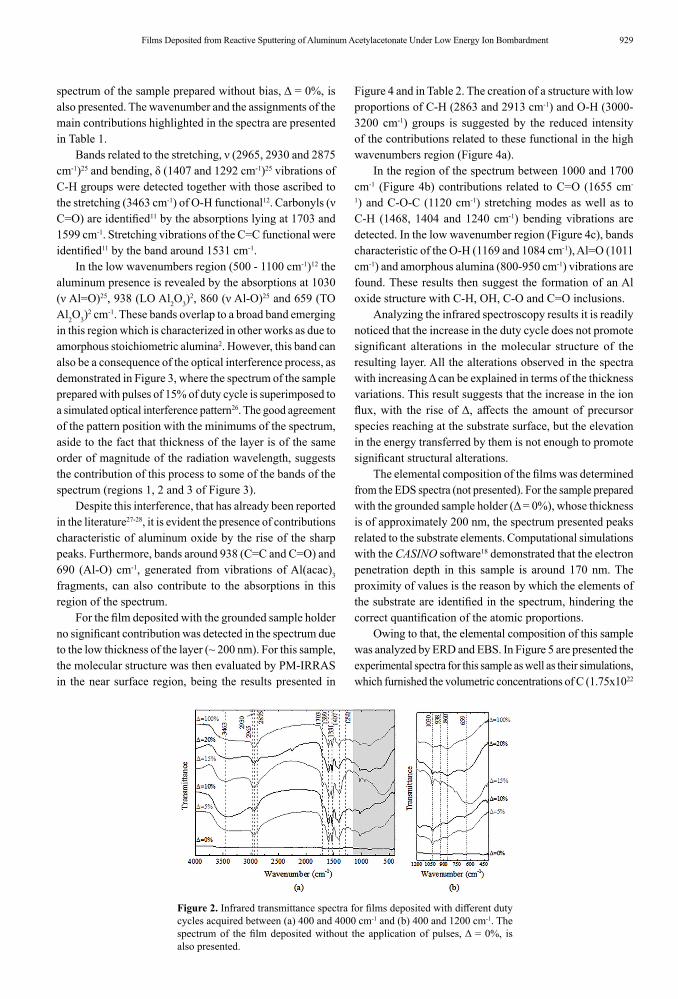
Figure 2 shows the infrared spectra of the films deposited using signals with different duty cycles (5 to 100%) in the 400 to 4000 cm-1 (a) and 400 to 1200 cm-1 (b) interval. The
929Films Deposited from Reactive Sputtering of Aluminum Acetylacetonate Under Low Energy Ion Bombardment
spectrum of the sample prepared without bias, Δ = 0%, is also presented. The wavenumber and the assignments of the main contributions highlighted in the spectra are presented in Table 1.
Bands related to the stretching, ν (2965, 2930 and 2875 cm-1)25 and bending, δ (1407 and 1292 cm-1)25 vibrations of C-H groups were detected together with those ascribed to the stretching (3463 cm-1) of O-H functional12. Carbonyls (ν C=O) are identified11 by the absorptions lying at 1703 and 1599 cm-1. Stretching vibrations of the C=C functional were identified11 by the band around 1531 cm-1.
In the low wavenumbers region (500 - 1100 cm-1)12 the aluminum presence is revealed by the absorptions at 1030 (ν Al=O)25, 938 (LO Al2O3)
2, 860 (ν Al-O)25 and 659 (TO Al2O3)
2 cm-1. These bands overlap to a broad band emerging in this region which is characterized in other works as due to amorphous stoichiometric alumina2. However, this band can also be a consequence of the optical interference process, as demonstrated in Figure 3, where the spectrum of the sample prepared with pulses of 15% of duty cycle is superimposed to a simulated optical interference pattern26. The good agreement of the pattern position with the minimums of the spectrum, aside to the fact that thickness of the layer is of the same order of magnitude of the radiation wavelength, suggests the contribution of this process to some of the bands of the spectrum (regions 1, 2 and 3 of Figure 3).
Despite this interference, that has already been reported in the literature27-28, it is evident the presence of contributions characteristic of aluminum oxide by the rise of the sharp peaks. Furthermore, bands around 938 (C=C and C=O) and 690 (Al-O) cm-1, generated from vibrations of Al(acac)3 fragments, can also contribute to the absorptions in this region of the spectrum.
For the film deposited with the grounded sample holder no significant contribution was detected in the spectrum due to the low thickness of the layer (~ 200 nm). For this sample, the molecular structure was then evaluated by PM-IRRAS in the near surface region, being the results presented in
Figure 4 and in Table 2. The creation of a structure with low proportions of C-H (2863 and 2913 cm-1) and O-H (3000-3200 cm-1) groups is suggested by the reduced intensity of the contributions related to these functional in the high wavenumbers region (Figure 4a).
In the region of the spectrum between 1000 and 1700 cm-1 (Figure 4b) contributions related to C=O (1655 cm-
1) and C-O-C (1120 cm-1) stretching modes as well as to C-H (1468, 1404 and 1240 cm-1) bending vibrations are detected. In the low wavenumber region (Figure 4c), bands characteristic of the O-H (1169 and 1084 cm-1), Al=O (1011 cm-1) and amorphous alumina (800-950 cm-1) vibrations are found. These results then suggest the formation of an Al oxide structure with C-H, OH, C-O and C=O inclusions.
Analyzing the infrared spectroscopy results it is readily noticed that the increase in the duty cycle does not promote significant alterations in the molecular structure of the resulting layer. All the alterations observed in the spectra with increasing Δ can be explained in terms of the thickness variations. This result suggests that the increase in the ion flux, with the rise of Δ, affects the amount of precursor species reaching at the substrate surface, but the elevation in the energy transferred by them is not enough to promote significant structural alterations.
The elemental composition of the films was determined from the EDS spectra (not presented). For the sample prepared with the grounded sample holder (Δ = 0%), whose thickness is of approximately 200 nm, the spectrum presented peaks related to the substrate elements. Computational simulations with the CASINO software18 demonstrated that the electron penetration depth in this sample is around 170 nm. The proximity of values is the reason by which the elements of the substrate are identified in the spectrum, hindering the correct quantification of the atomic proportions.
Owing to that, the elemental composition of this sample was analyzed by ERD and EBS. In Figure 5 are presented the experimental spectra for this sample as well as their simulations, which furnished the volumetric concentrations of C (1.75x10²²
Figure 2. Infrared transmittance spectra for films deposited with different duty cycles acquired between (a) 400 and 4000 cm-1 and (b) 400 and 1200 cm-1. The spectrum of the film deposited without the application of pulses, Δ = 0%, is also presented.

Battaglin et al.930 Materials Research
Table 1. Wavenumber of the absorption bands present in the infrared spectra of the films deposited with different duty cycles as well as their assignments.
Wavenumber (cm-1) Assignment
3463 ν O-H
2965 ν C-H
2930 ν C-H
2875 ν C-H
1703 ν C=O
1599 ν C=O
1531 ν C=C
1407 δ C-H
1292 δ C-H
1030 ν Al=O
938LO Al2O3 (*957 cm-1)
ν C=C e ν C=O (Al(acac)3)
860 ν Al-O
659TO Al2O3 (*630 cm-1)
Al-O (Al(acac)3)Notes: LO - Longitudinal optical mode of amorphous alumina. TO - Transversal optical mode of amorphous alumina.(*) Reference: YAMADA-TAKAMURA et al.2.
Figure 3. Infrared transmittance spectrum for the sample deposited with Δ = 15% (solid line) and sinusoidal simulated curve for an optical interference process (hatched line). The circles highlight the parts of the spectrum in which the optical interference contributes to the intensities of the bands of the spectrum.
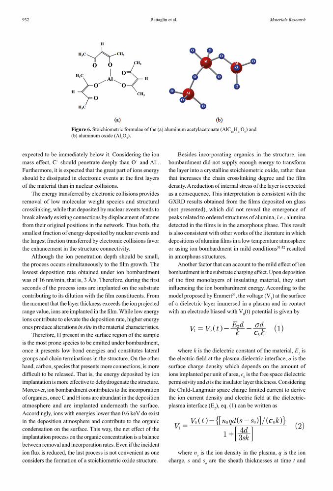
atoms/cm3), O (3.69x10²² atoms/cm3), Al (0.92x10²² atoms/cm3) and H (1.36x10²² atoms/cm3). From these results, and disregarding H, it was found that the film deposited without biasing the holder presents 28 at.% of C, 58 at.% of O and 14 at.% of Al. To analyze this result, it must be considered that the Al(acac)3 molecule, schematically illustrated in Figure 6a, presents 68 at.% of C, 27 at.% of O and 5 at.% of Al. That is, homogeneous and heterogeneous reactions occurring in the deposition process substantially reduce the concentration of
C and raise those of Al and O initially present in the precursor molecule. Comparing the stoichiometry of this sample with the expected for the aluminum oxide, Al2O3 (Figure 6b), that is, Al = 40 at.% and O = 60 at.%, it can be noticed a good agreement in the O proportion but a great discrepancy in the Al one due to the presence of organics (C-H, C=O, C=C, C-O-C). These results are consistent with the obtained by infrared spectroscopy and with the presented by Schmidt et al.29 which demonstrated increasing C concentrations in aluminum oxide films deposited from the pyrolysis of the dimethylaluminum isopropoxide via high-vacuum chemical vapor deposition, when the deposition temperature was increased up to 659ºC.
The volumetric concentration of the elements, determined from the EBS and ERD results, also allows to infer on the deposition mechanism when H proportion is taken into account in the calculations. For the film deposited with the grounded holder there is 23 at.% of C, 48 at.% of O, 12 at.% of Al and 17 at.% of H whereas the expected for the precursor molecule (AlC15H21O6) is of 35 at.% of C, 14 at.% of O, 2 at.% of Al and 49 at.% of H. That is, for the transformation of the Al(acac)3 precursor into the film, the C proportion must be reduced in 12 percentage points whereas that of H in 32 percentage points, showing that H removal is greater than the C one. The abundance of active oxygen in the plasma phase stimulates the recombination of this element with H and C of the fragments generating low sticking coefficient groups (OH, H2O, CO, CO2) which are eventually removed from the deposition atmosphere by the vacuum system.
The atomic proportions obtained from the EDS spectra for the other samples are roughly the same: 73 at.% of C, 22 at.% of O and 5 at.% of Al, i.e., the increase in temperature generated by the duty cycle variation over again didn’t affect the concentration of the films. Comparing these results with the obtained for the sample deposited with the grounded holder, turns evident that the association of ion bombardment raises the C proportion but reduces the O and Al content, indicating that carbon ions are abundant in the plasma and effectively contribute to the deposition when they are attracted to the substrate. In other words, larger oxygen proportions than the used in this work (25%) and changes in the parameters would be necessary in the plasma to provide carbon removal in a more efficient way.
Besides, independently of the duty cycle condition used, the concentration of elements constituents of the film remains constant. This behavior is explained by the fact that all the depositions occurred under the same plasma conditions as one considers the chemical composition, gas pressure and excitation power. As a result, the plasma mechanism responsible for the Al(acac)3 sputtering, remained unchanged, resulting in similar precursor species in all the deposition cycles. The variation of the duty cycle, on its turn, influenced only the amount of these species that arrived at the substrate, what is confirmed by the thickness variations.

931Films Deposited from Reactive Sputtering of Aluminum Acetylacetonate Under Low Energy Ion Bombardment
Figure 4. PM-IRRAS spectrum of the film deposited in the grounded holder, taken in the (a) 2700-3200 cm-1, (b) 1000-1700 cm-1 and (c) 800-1200 cm-1 regions.
Table 2. Wavenumber of the absorption bands present in the PM-IRRAS spectrum of the film deposited with no bias pulses.
Wavenumber (cm-¹) Assignment
3000-3200 ν O-H
2913 ν C-H
2863 ν C-H
1655 ν C=O
1468 δ C-H
1404 δ C-H
1240 δ C-H
1120 ν C-O-C
1169 δ O-H
1084 δ O-H
1011 ν Al=O
800-950LO Al2O3 (*957 cm-1)
and/or ν Al-O (**860 cm-1)Notes: LO: Longitudinal optical mode of amorphous alumina.(*) from YAMADA-TAKAMURA et al.2. (**) from NIELSEN et al.11.
Figure 5. Experimental data (dots) with the simulated spectrum for the sample prepared with the grounded holder, for (a) EBS (C, O, Al) and (b) ERD (H) measurements.
3.3. Energy deposition mechanisms and crystalline structure
Considering the bottom (4.3 Pa) and total (11.0 Pa) pressures employed in this work, it is expected that plasma has a large amount of atmospheric impurities (CO2, O2 and H2O) and also species with energies lower than 0.6 keV (low free path of species). In addition, the breakdown of the precursor molecule generates fragments (CHx, C-O, AlOx and etc), contributing to the ion bombardment process not involving only Al+, O+, H+ and C+ ions. Thus, despite the impossibility of considering these factors in the simulations, the results obtained for the Al+, O+, H+ and C+ ions have fundamental role in understanding the energy transfer mechanism to the layer. The project range for Al+, C+ and O+ are expected to be practically the same while that for H+ should be substantially higher owing to the reduced cross section of this species30. A large fraction of implanted ions should lie on film-air interface, but most of them are
Battaglin et al.932 Materials Research
Figure 6. Stoichiometric formulae of the (a) aluminum acetylacetonate (AlC15H21O6) and (b) aluminum oxide (Al2O3).
expected to be immediately below it. Considering the ion mass effect, C+ should penetrate deeply than O+ and Al+. Furthermore, it is expected that the great part of ions energy should be dissipated in electronic events at the first layers of the material than in nuclear collisions.
The energy transferred by electronic collisions provides removal of low molecular weight species and structural crosslinking, while that deposited by nuclear events tends to break already existing connections by displacement of atoms from their original positions in the network. Thus both, the smallest fraction of energy deposited by nuclear events and the largest fraction transferred by electronic collisions favor the enhancement in the structure connectivity.
Although the ion penetration depth should be small, the process occurs simultaneously to the film growth. The lowest deposition rate obtained under ion bombardment was of 16 nm/min, that is, 3 Å/s. Therefore, during the first seconds of the process ions are implanted on the substrate contributing to its dilution with the film constituents. From the moment that the layer thickness exceeds the ion projected range value, ions are implanted in the film. While low energy ions contribute to elevate the deposition rate, higher energy ones produce alterations in situ in the material characteristics.
Therefore, H present in the surface region of the sample is the most prone species to be emitted under bombardment, once it presents low bond energies and constitutes lateral groups and chain terminations in the structure. On the other hand, carbon, species that presents more connections, is more difficult to be released. That is, the energy deposited by ion implantation is more effective to dehydrogenate the structure. Moreover, ion bombardment contributes to the incorporation of organics, once C and H ions are abundant in the deposition atmosphere and are implanted underneath the surface. Accordingly, ions with energies lower than 0.6 keV do exist in the deposition atmosphere and contribute to the organic condensation on the surface. This way, the net effect of the implantation process on the organic concentration is a balance between removal and incorporation rates. Even if the incident ion flux is reduced, the last process is not convenient as one considers the formation of a stoichiometric oxide structure.
Besides incorporating organics in the structure, ion bombardment did not supply enough energy to transform the layer into a crystalline stoichiometric oxide, rather than that increases the chain crosslinking degree and the film density. A reduction of internal stress of the layer is expected as a consequence. This interpretation is consistent with the GXRD results obtained from the films deposited on glass (not presented), which did not reveal the emergence of peaks related to ordered structures of alumina, i.e., alumina detected in the films is in the amorphous phase. This result is also consistent with other works of the literature in which depositions of alumina films in a low temperature atmosphere or using ion bombardment in mild conditions31-32 resulted in amorphous structures.
Another factor that can account to the mild effect of ion bombardment is the substrate charging effect. Upon deposition of the first monolayers of insulating material, they start influencing the ion bombardment energy. According to the model proposed by Emmert33, the voltage (V1) at the surface of a dielectric layer immersed in a plasma and in contact with an electrode biased with V0(t) potential is given by
( )V V t kE d
kd 11 0
2
0ev= - -Q V
where k is the dielectric constant of the material, E2 is the electric field at the plasma-dielectric interface, σ is the surface charge density which depends on the amount of ions implanted per unit of area, ϵ0 is the free space dielectric permissivity and d is the insulator layer thickness. Considering the Child-Langmuir space charge limited current to derive the ion current density and electric field at the dielectric-plasma interface (E2), eq. (1) can be written as
/( )V
skd
V t n qd s s k
1 34 21
0 0 0 0e=
+
- -Q Q QV V V"
# &
%F I
where no is the ion density in the plasma, q is the ion charge, s and so are the sheath thicknesses at time t and

933Films Deposited from Reactive Sputtering of Aluminum Acetylacetonate Under Low Energy Ion Bombardment
The films deposited using bias signals with duty cycles between 5 and 20% (Figure 8b-e) present cracks, consistently with the higher thickness of these layers in comparison to the obtained with the ground holder. The size of the particulates sit on the surface grows while the smallest ones disappear. It is postulated that ion bombardment furnishes enough energy to fragment the surface clusters ejecting their constituents to the plasma or recoiling them underneath. Furthermore, grains immersed in a rather uniform film matrix are evidenced. Still for the same sample, the 2 µm x 2 µm topographical profile reveals a fine scale structure with pores (dark points) trapped on it, but still more regular than the deposited with no ion bombardment. This result is consistent with the loss of H and the consequent enhancement in the crosslinking degree. The concentration of defects in these structures is observed to correlate inversely with the deposited energy and directly with the deposition rate, i.e., it depends on the ratio between the concentration of neutral (low energy) species and of energetic ions reaching the surface.
The concentration of unconnected particulates was reduced in the sample deposited using Δ = 100% (Figure 8f) in comparison to the others. A highly defined granular structure, presenting no background matrix, is identified by the topographic profiles. The increase in the flux of the energetic particles impinging the layer explains the disappearance of the major grains. The greater definition of the granular matrix, caused by creation of extra sites (defects) where atomic and molecular precursors can start nucleation, is explained in terms of the same phenomenon.
In general, the surface microstructure evolved as the duty cycle of the bias signal was increased. A surface composed by an irregular matrix with particulates sparsely sit on it was shifted to granular but more regular one, ending up in a completely granular structure composed of highly defined grains. The cracks disappeared with increasing Δ, pointing to a greater crosslinking degree and to a reduction in the concentration of defects then lowering internal stress15, 32, 34.
t0, respectively. The second term in the numerator of eq. (2) indicates the surface charging effect induced by ion implantation. On its hand, the second term in the denominator represents the effect of the thickness and of the dielectric properties of the insulator on the voltage developed at the surface plasma interface.
The surface charge density in these equations depends on the pulse on-time and on remaining charges left on the surface by previous pulse application, showing that V1 vary with the pulse duty cycle. High duty cycles, conditions in which the on-time is longer, will produce higher charge densities on the surface reducing the ion accelerating potential (V1). Therefore, in the experiments performed here, the influence of the surface charging is expected to rise with increasing pulse duty cycle.
3.4. Morphology and topography
Figure 7 shows the secondary electron micrograph for the bare stainless steel and the two dimensional topographic profile of the glass plate, respectively used as substrates of the samples submitted to morphological and topographical analysis. The micrograph of the steel reveals a smooth surface containing scratches. The glass substrate presents regular topography with some defects, generated by both the manufacturing process and the cleaning procedure to which the samples were submitted.
The micrographs and topographic profiles of the film containing samples are presented in Figure 8. For the film deposited with the grounded holder (Figure 8a), the surface follows the substrate imperfections, once the thickness of the layer is reduced (~ 200 nm). In the 20 µm x 20 µm topographical profile particles with different dimensions sit on the surface are identified. From the 2 µm x 2 µm profile it is realized the granular nature of the film, characteristic of alumina structures4, and the incorporation of pores due to low energy species deposition.
Figure 7. (a) Secondary electron micrograph of the as-received stainless steel. (b) AFM topographic profile for the glass substrate.

Battaglin et al.934 Materials Research
Figure 8. Secondary electron micrographs (left) and topographic profiles (right and insert) for the films deposited using bias signals with duty cycles between 0 and 100%.
In short, the energy deposited by ion bombardment changes the morphology and physical stability of the samples.
The RMS roughness of the samples, evaluated from the 20 μm x 20 μm profiles, is presented in Figure 9 as function
Figure 9. RMS roughness of the films as function of the duty cycle of the bias signal. The dotted line represents the roughness for the bare glass substrate. The inserts represent 3D topographic profiles of the corresponding samples.
of the duty cycle of the pulses. The dotted line in this figure represents the roughness of the bare glass substrate. Duty cycle is observed to affect the roughness of the films consistently with the topographical evolution observed in the samples profiles. The roughness values found here are similar to those reported by Nakao et al.32 for alumina films that suffered post deposition ion bombardment.
4. Conclusions
The association of ion bombardment to the reactive sputtering of Al(acac)3 affects the thickness, chemical composition, morphology, topography and roughness of the samples, transforming the organic-containing alumina into an organic material with oxide inclusions.
The ions present in the deposition process are implanted in the film-air interface or underneath the surface. The dissipated energy does not effectively promote organic removal. Instead, the abundance of organic ions in the deposition atmosphere turns their implantation a contamination source for the process. The more evident chemical changes induced by ion bombardment are related to the loss of hydrogen, since carbon is more interconnected. Under the conditions employed here, ion bombardment does not provide enough energy to promote precipitation of crystalline phases of alumina.
Controlling the duty cycle of the bias signal enables to tailor the concentration of charged fragments reaching the substrate, but not the fragment type, defined by the reactive sputtering conditions. Surface microstructure and roughness are influenced by the duty cycle of the pulses while chemical composition is barely affected. The crosslinking probability is increased by the preferential loss of H, changing the overall structural conformation.
In general, the association of ion bombardment to the deposition process was beneficial as one considers the better physical stability of the resulting films while keeping their

935Films Deposited from Reactive Sputtering of Aluminum Acetylacetonate Under Low Energy Ion Bombardment
high thicknesses. The optimum condition was considered that which employed continuous bias (Δ = 100%) due to the convenient physical properties of the film, the greater simplicity and lower cost of the equipment. However, it did not favor the formation of stoichiometric alumina or the precipitation of crystalline phases of this material.
Considering the base (4.2 Pa) and working (11.0 Pa) pressures employed here, a great amount of impurities (CO2, atmospheric O2 and H2O) is expected to take part of the deposition. However, the main contaminants of the structure still are C and H, coming from the precursor compound. Since organic incorporation is a consequence of the incomplete fragmentation of the precursor, the refinement of this methodology is based on changes in the oxygen proportion diluted in the deposition atmosphere. To increase the ion bombardment energy while reducing the ion flux are possibilities that can also provide less organic contamination, as reported in other works. Finally, higher energies should be provided to the growing layer by reducing the pressure during deposition, increasing the intensity and time of the bias pulses, applying resistive heating or combining them to promote the transformation of an amorphous structure into a crystalline one.
5. Acknowledgments
The authors would like to thank LNNano (National Laboratory of Nanotechnology)/CNPEM (Campinas Brazil) for the AFM analysis and the financial support supplied by FAPESP (2012/14708-2) and CNPq (303662/2015-8) for this project.
6. References
1. Rodriguez P, Caussat B, Iltis X, Ablitzer C, Brothier M. Alumina coatings on silica powders by Fluidized Bed Chemical Vapor Deposition from aluminium acetylacetonate. Chemical Engineering Journal. 2012;211-212:68-76.
2. Yamada-Takamura Y, Koch F, Maier H, Bolt H. Characterization of α-phase aluminum oxide films deposited by filtered vacuum arc. Surface and Coatings Technology. 2001;142-144:260-264.
3. Natali M, Carta G, Rigato V, Rossetto G, Salmaso G, Zanella P. Chemical, morphological and nano-mechanical characterizations of Al2O3 thin films deposited by metal organic chemical vapour deposition on AISI 304 stainless steel. Electrochimica Acta. 2005;50(23):4615-4620.
4. Cibert C, Hidalgo H, Champeaux C, Tristant P, Tixier C, Desmaison J, et al. Properties of aluminum oxide thin films deposited by pulsed laser deposition and plasma enhanced chemical vapor deposition. Thin Solid Films. 2008;516(6):1290-1296.
5. Lin CH, Wang HL, Hon MH. Preparation and characterization of aluminum oxide films by plasma enhanced chemical vapor deposition. Surface and Coatings Technology. 1997;90(1-2):102-106.
6. Zhao YW, Suhr H. Aluminium oxide thin films prepared by plasma-enhanced chemical vapour deposition. Applied Physics A. 1992;55(2):176-179.
7. Kyrylov O, Cremer R, Neuschütz D. Deposition of alumina hard coatings by bipolar pulsed PECVD. Surface and Coatings Technology. 2003;163-164:203-207.
8. Sarakinos K, Music D, Nahif F, Jiang K, Braun A, Zilkens C, et al. Ionized physical vapor deposited Al2O3 films: Does subplantation favor formation of α-Al2O3? Physica Status Solidi: Rapid Research Letters. 2010;4(7):154-156.
9. Koo J, Kim S, Jeon S, Jeon H, Kim Y, Won Y. Characteristics of Al2O3 Thin Films Deposited Using Dimethylaluminum Isopropoxide and Trimethylaluminum Precursors by the Plasma-Enhanced Atomic-Layer Deposition Method. Journal of the Korean Physical Society. 2006;48(1):131-136.
10. Mahnke M, Wiechmann S, Heider HJ, Blume O, Müller J. Aluminum Oxide Doped with Erbium, Titanium and Chromium for Active Integrated Optical Applications. AEU -International Journal of Electronics and Communications. 2001;55(5):342-348.
11. Nielsen GF, Silva LHF, Cruz NC, Rangel EC. Preparation of films from aluminum acetylacetonate by plasma sputtering. Surface and Interface Analysis. 2013;45(7):1113-1118.
12. Maruyama T, Arai S. Aluminum oxide thin films prepared by chemical vapor deposition from aluminum acetylacetonate. Applied Physics Letters. 1992;60(3):322.
13. Muhsin AE. Chemical Vapor Deposition of Aluminum Oxide (Al2O3) and Beta Iron Disilicide (β-FeSi2) Thin Films. [Thesis]. Duisburg: Universität Duisburg-Essen; 2007.
14. Battaglin FAD, Hosokawa RS, Cruz NC, Caseli L, Rangel EC, Silva TF, et al. Innovative low temperature plasma approach for deposition of alumina films. Materials Research. 2014;17(6):1410-1419.
15. Konstantinidis S, Jiang K, Roobroek A, Renaux F, Schneider JM. Pulsed Plasma Enhanced Chemical Vapor Deposition of Alumina Thin Films: Influence of the Duty Cycle on Structure and Elastic Properties. Plasma Processes and Polymers. 2011;8(7):651-657.
16. Rangel RCC, Souza MEP, Schreiner WH, Freire CMA, Rangel EC, Cruz NC. Effect of the fluorination of DLC film on the corrosion protection of aluminum alloy (AA 5052). Surface and Coatings Technology. 2010;204(18-19):3022-3028.
17. Leng Y. Materials Characterization: Introduction to Microscopic and Spectroscopic Methods. Singapore: John Wiley and Sons (Asia); 2008.
18. Hovington P, Drouin D, Gauvin R. CASINO: a new monte carlo code in C language for electron beam interaction - part I: description of the program. Scanning. 1997;19(1):1-14.
19. Jeynes C. Elastic Backscattering of Ions for Compositional Analysis. In: Kaufmann EN, ed. Characterization of Materials. Hoboken: Wiley; 2012. p. 1-21.
20. Silva TF, Rodrigues CL, Mayer M, Moro MV, Trindade GF, Aguirre FR, et al. MultiSIMNRA: A computational tool for self-consistent ion beam analysis using SIMNRA. Nuclear Instruments and Methods in Physics Research
Battaglin et al.936 Materials Research
Section B: Beam Interactions with Materials and Atoms. 2016;371:86-89.
21. Mayer M. SIMNRA: a simulation program for the analysis of NRA, RBS and ERDA. AIP Conference Proceedings. 1999;475(1):541.
22. Gurbich AF. SigmaCalc recent development and present status of the evaluated cross-sections for IBA. Nuclear Instruments and Methods in Physics Research Section B: Beam Interactions with Materials and Atoms. 2016;371:27-32.
23. Cheng HS, Shen H, Yang F, Tang JY. Cross sections for non-Rutherford backscattering of 4He from five light elements. Nuclear Instruments and Methods in Physics Research Section B: Beam Interactions with Materials and Atoms. 1994;85(1-2):47-50.
24. Prado ES. Técnica híbrida de plasma para deposição de filmes de alumina. [Dissertation]. Bauru: Universidade Estadual Paulista Júlio de Mesquita Filho; 2015. 102 f.
25. Nielsen GF. Filmes orgânicos contendo óxido de alumínio depositados a plasma. [Dissertation]. Bauru: Universidade Estadual Paulista Júlio de Mesquita Filho; 2011. 81 f.
26. Rangel EC, Machida M, Durrant SF, Cruz NC. A Novel Plasma Technique for Surface Treatment: The Plasma Expander. IEEE Transactions on Plasma Science. 2012;40(2):492-496.
27. Rangel EC, Cruz NC, Lepienski M, Moraes MAB, Lepienski CM. Influence of Ar+ ion irradiation on the properties of plasma polymerized acetylene films. Surface and Coatings Technology. 2000;127(1):93-98.
28. Rangel EC. Implantação iônica em filmes finos depositados por PECVD. [Thesis]. Campinas: Universidade Estadual de Campinas; 1999.
29. Schmidt BW, Rogers BR, Gren CK, Hanusa TP. Carbon incorporation in chemical vapor deposited aluminum oxide films. Thin Solid Films. 2010;518(14):3658-3663.
30. Sant’Ana PL. Plásticos comerciais tratados a plasma para dispositivos ópticos e embalagens alimentícias. [Thesis]. Bauru: Universidade Estadual Paulista Júlio de Mesquita Filho; 2014. 109 f.
31. Chryssou CE, Pitt CW. Al2O3 thin films by plasma-enhanced chemical vapour deposition using trimethyl-amine alane (TMAA) as the Al precursor. Applied Physics A. 1997;65(4):469-475.
32. Nakao S, Jin P, Xu G, Ikeyama M, Miyagawa Y, Miyagawa S. Crystallization of amorphous alumina films induced by high-energy ion irradiation. Journal of Crystal Growth. 2002;237-239(Pt 1):580-585.
33. Emmert GA. Model for expanding sheaths and surface charging at dielectric surfaces during plasma source ion implantation. Journal of Vacuum Science & Technology B, Nanotechnology and Microelectronics: Materials, Processing, Measurement, and Phenomena. 1994;12(2):880.
34. Nable JC, Suib SL, Galasso FS. Metal organic chemical vapor deposition of Al2O3 and Cr2O3 on nickel as oxidation barriers. Surface and Coatings Technology. 2004;186(3):423-430.