review of nanocomposite thin films and coatings deposited by
TRANSCRIPT
7
Review of Nanocomposite Thin Films and Coatings Deposited by PVD and CVD Technology
Krzysztof Lukaszkowicz Silesian University of Technology
Poland
1. Introduction
Commonly it is assumed that the nanocrystalline materials are composed of elements like grains, crystallites, layers, e.g., of a size of ca. 100 nm. (more typically less than 50 nm; often less than 10 nm – in the case of superhard nanocomposite, materials for optoelectronic applications, etc.) at least in one direction. The definition give above limits the size of the structure elements, however it has to be seen only as a theoretical value and doesn’t have any physical importance. Thin films and coatings are applied to structural bulk materials in order to improve the desired properties of the surface, such as corrosion resistance, wear resistance, hardness, friction or required colour, e.g., golden, black or a polished brass-like. The research issues concerning the production of coatings are one of the more important directions of surface engineering development, ensuring the obtainment of coatings of high utility properties in the scope of mechanical characteristics and wear resistance. Giving new utility characteristics to commonly known materials is frequently obtained by laying simple monolayer, multilayer or gradient coatings using PVD methods (Dobrzanski et al., 2005; Lukaszkowicz & Dobrzanski, 2008). While selecting the coating material, we encounter a barrier caused by the fact that numerous properties expected from an ideal coating are impossible to be obtained simultaneously. The application of the nanostructure coatings is seen as the solution of this issue. Nanostructure and particularly nanocomposite coatings deposited by physical vapour deposition or chemical vapour deposition, have gained considerable attention due to their unique physical and chemical properties, e.g. extremely high indentation hardness (40-80 GPa) (Veprek et al., 2006, 2000; Zou et al., 2010), corrosion resistance (Audronis et al., 2008; Lukaszkowicz et al., 2010), excellent high temperature oxidization resistance (Vaz et al., 2000; Voevodin & Zabinski, 2005), as well high abrasion and erosion resistance (Cheng et al., 2010; Polychronopoulou et al., 2009; Veprek & Veprek-Heijman, 2008). In the present work, the emphasis is put on current practices and future trends for
nanocomposite thin films and coatings deposited by physical vapour deposition (PVD) and
chemical vapour deposition (CVD) techniques. This review will not be so exhaustive as to
cover all aspects of such coatings, but the main objective is to give a general sense of what
has so far been accomplished and where the field is going.
www.intechopen.com
Nanomaterials
146
2. Synthesis of nanocomposite films and coatings
In conventional bulk materials, refining grain size is one of the possibilities for hardness
increase. The same is true for nanocomposite films or coatings. Looking for coating
materials with high hardness, higher then the hardness of traditional polycrystalline
coatings, there are founding materials with unique nanometric structure properties. With a
decrease in grain size, the multiplication and mobility of the dislocations are hindered, and
the hardness of materials increase according to the Hall-Petch relationship. This effect is
especially prominent for grain size down to tens of nanometers. However, dislocation
movement, which determines the hardness in conventional materials, has little effect when
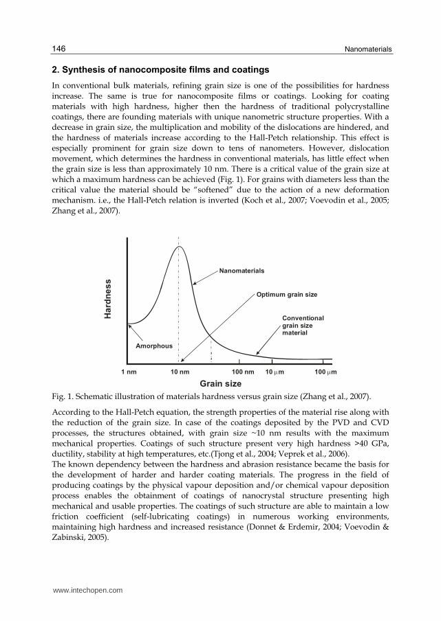
the grain size is less than approximately 10 nm. There is a critical value of the grain size at
which a maximum hardness can be achieved (Fig. 1). For grains with diameters less than the
critical value the material should be “softened” due to the action of a new deformation
mechanism. i.e., the Hall-Petch relation is inverted (Koch et al., 2007; Voevodin et al., 2005;
Zhang et al., 2007).
1 nm 10 nm 100 nm 10 m 100 m Grain size
Ha
rdn
es
s
Nanomaterials
Optimum grain size
Conventionalgrain sizematerial
Amorphous
Fig. 1. Schematic illustration of materials hardness versus grain size (Zhang et al., 2007).
According to the Hall-Petch equation, the strength properties of the material rise along with
the reduction of the grain size. In case of the coatings deposited by the PVD and CVD
processes, the structures obtained, with grain size ~10 nm results with the maximum
mechanical properties. Coatings of such structure present very high hardness >40 GPa,
ductility, stability at high temperatures, etc.(Tjong et al., 2004; Veprek et al., 2006).
The known dependency between the hardness and abrasion resistance became the basis for
the development of harder and harder coating materials. The progress in the field of
producing coatings by the physical vapour deposition and/or chemical vapour deposition
process enables the obtainment of coatings of nanocrystal structure presenting high
mechanical and usable properties. The coatings of such structure are able to maintain a low
friction coefficient (self-lubricating coatings) in numerous working environments,
maintaining high hardness and increased resistance (Donnet & Erdemir, 2004; Voevodin &
Zabinski, 2005).
www.intechopen.com
Review of Nanocomposite Thin Films and Coatings Deposited by PVD and CVD Technology
147
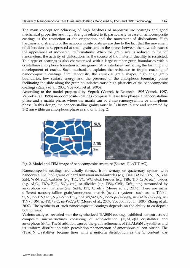
The main concept for achieving of high hardness of nanostructure coatings and good mechanical properties and high strength related to it, particularly in case of nanocomposite coatings is the restriction of the origination and the movement of dislocations. High hardness and strength of the nanocomposite coatings are due to the fact that the movement of dislocations is suppressed at small grains and in the spaces between them, which causes the appearance of incoherent deformations. When the grain size is reduced to that of nanometers, the activity of dislocations as the source of the material ductility is restricted. This type of coatings is also characterized with a large number grain boundaries with a crystalline/amorphous transition across grain-matrix interfaces, restricting the forming and development of cracks. Such mechanism explains the resistance to fragile cracking of nanocomposite coatings. Simultaneously, the equiaxial grain shapes, high angle grain boundaries, low surface energy and the presence of the amorphous boundary phase facilitating the slide along the grain boundaries cause high plasticity of the nanocomposite coatings (Rafaja et al., 2006; Voevodin et al., 2005). According to the model proposed by Veprek (Veprek & Reiprech, 1995;Veprek, 1997, Veprek et al., 1998) nanocomposite coatings comprise at least two phases, a nanocrystalline phase and a matrix phase, where the matrix can be either nanocrystalline or amorphous phase. In this design, the nanocrystalline grains must be 3÷10 nm in size and separated by 1÷2 nm within an amorphous phase as shown in Fig. 2.
Fig. 2. Model and TEM image of nanocomposite structure (Source: PLATIT AG).
Nanocomposite coatings are usually formed from ternary or quaternary system with nanocrystalline (nc-) grains of hard transition metal-nitrides (e.g. TiN, TiAlN, CrN, BN, VN, ZrN, W2N, etc.), carbides (e.g. TiC, VC, WC, etc.), borides (e.g. TiB2, TiB, CrB2, etc.), oxides (e.g. Al2O3, TiO2, B2O3, SiO2, etc.), or silicides (e.g. TiSi2, CrSi2, ZrSi2, etc.) surrounded by amorphous (a-) matrices (e.g. Si3N4, BN, C, etc.) (Moore et al., 2007). There are many different nanocrystalline grain/amorphous matrix (nc-/a-) systems, such as: nc-TiN/a-Si3N4, nc-TiN/a-Si3N4/a-&nc-TiSi2, nc-CrN/a-Si3N4, nc-W2N/a-Si3N4, nc-TiAlN/a-Si3N4, nc-TiN/a-BN, nc-TiC/a-C, nc-WC/a-C (Moore et al., 2007, Voevodin et al., 2005; Zhang et al., 2007). The synthesis of such nanocomposite coatings depends on the ability to co-deposit both phases. Various analyses revealed that the synthesized TiAlSiN coatings exhibited nanostructured composite microstructures consisting of solid-solution (Ti,Al,Si)N crystallites and amorphous Si3N4. The Si addition caused the grain refinement of (Ti,Al,Si)N crystallites and its uniform distribution with percolation phenomenon of amorphous silicon nitride. The (Ti,Al)N crystallites became finer with a uniform distribution as the Si content was
www.intechopen.com
Nanomaterials
148
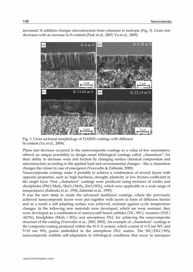
increased. Si addition changes microstructure from columnar to isotropic (Fig. 3). Grain size decreases with an increase in Si content (Park et al., 2003; Yu et al., 2009).
Fig. 3. Cross sectional morphology of TiAlSiN coatings with different Si content (Yu et al., 2009).
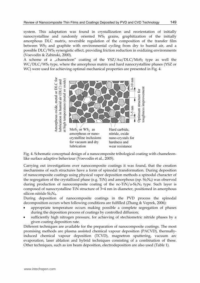
Phase size decrease occurred in the nanocomposite coatings to a value of few nanometers, offered an unique possibility to design smart tribological coatings called „chameleon”, for their ability to decrease wear and friction by changing surface chemical composition and microstructure according to the applied load and environmental changes – like a chameleon changes the colour in case of emergence (Voevodin & Zabinski, 2000). Nanocomposite coatings make it possible to achieve a combination of several layers with opposite properties, such as: high hardness, strength, plasticity or low friction coefficient in the single layer. First „chameleon” coatings were produced using mixtures of oxides and disulphides (PbO/MoS2, Sb2O3/MoS2, ZnO/WS2), which were applicable in a wide range of temperatures (Zabinski et al., 1992; Zabinski et al., 1993). It was the next steep to create the advanced multilayer coatings, where the previously achieved nanocomposite layers were put together with layers in form of diffusion barrier and as a result a self adapting surface was achieved, resistant against cyclic temperature changes. In the following new materials were developed, which are wear resistant, they were developed as a combination of nanocrystall based carbides (TiC, WC), ceramics (YSZ i AlON), bisulphites (MoS2 i WS2) and amorphous DLC for achieving the nanocomposite structure of the coating (Voevodin et al., 2001; 2002). An example of „chameleon” coatings is the composite coating produced within the W-C-S system, which consist of 1÷2 nm WC and 5÷10 nm WS2 grains embedded in the amorphous DLC matrix. The WC/DLC/WS2 nanocomposite exhibits self-adaptation to tribological conditions that occur in aerospace
www.intechopen.com
Review of Nanocomposite Thin Films and Coatings Deposited by PVD and CVD Technology
149
system. This adaptation was found in crystallization and reorientation of initially nanocrystalline and randomly oriented WS2 grains, graphitization of the initially amorphous DLC matrix, reversible regulation of the composition of the transfer film between WS2 and graphite with environmental cycling from dry to humid air, and a possible DLC/WS2 synergistic effect, providing friction reduction in oxidizing environments (Voevodin & Zabinski, 2000). A scheme of a „chameleon” coating of the YSZ/Au/DLC/MoS2 type as well the WC/DLC/WS2 type, where the amorphous matrix and hard nanocrystalline phases (YSZ or WC) were used for achieving optimal mechanical properties are presented in Fig. 4.
Fig. 4. Schematic conceptual design of a nanocomposite tribological coating with chameleon-like surface adaptive behaviour (Voevodin et al., 2005).
Carrying out investigations over nanocomposite coatings it was found, that the creation mechanisms of such structures have a form of spinodal transformation. During deposition of nanocomposite coatings using physical vapor deposition methods a spinodal character of the segregation of the crystallized phase (e.g. TiN) and amorphous (np. Si3N4) was observed during production of nanocomposite coating of the nc-TiN/a-Si3N4 type. Such layer is composed of nanocrystalline TiN structure of 3÷4 nm in diameter, positioned in amorphous silicon nitride Si3N4. During deposition of nanocomposite coatings in the PVD process the spinodal decomposition occurs when following conditions are fulfilled (Zhang & Veprek, 2006):
appropriate temperature occurs making possible a complete segregation of phases during the deposition process of coatings by controlled diffusion;
sufficiently high nitrogen pressure, for achieving of stechiometric nitride phases by a given coating deposition rate.
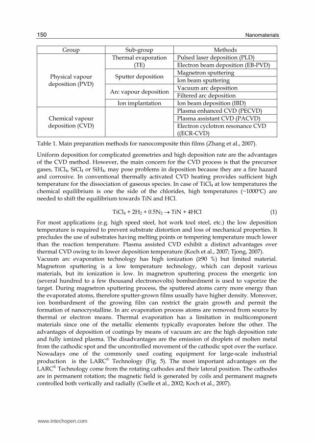
Different techniques are available for the preparation of nanocomposite coatings. The most promising methods are plasma assisted chemical vapour deposition (PACVD), thermally-induced chemical vapour deposition (TCVD), magnetron sputtering, vacuum arc evaporation, laser ablation and hybrid techniques consisting of a combination of these. Other techniques, such as ion beam deposition, electrodeposition are also used (Table 1).
www.intechopen.com
Nanomaterials
150
Group Sub-group Methods
Physical vapour deposition (PVD)
Thermal evaporation (TE)
Pulsed laser deposition (PLD)
Electron beam deposition (EB-PVD)
Sputter deposition Magnetron sputtering
Ion beam sputtering
Arc vapour deposition Vacuum arc deposition
Filtered arc deposition
Ion implantation Ion beam deposition (IBD)
Chemical vapour deposition (CVD)
Plasma enhanced CVD (PECVD)
Plasma assistant CVD (PACVD)
Electron cyclotron resonance CVD ((ECR-CVD)
Table 1. Main preparation methods for nanocomposite thin films (Zhang et al., 2007).
Uniform deposition for complicated geometries and high deposition rate are the advantages of the CVD method. However, the main concern for the CVD process is that the precursor gases, TiCl4, SiCl4 or SiH4, may pose problems in deposition because they are a fire hazard and corrosive. In conventional thermally activated CVD heating provides sufficient high temperature for the dissociation of gaseous species. In case of TiCl4 at low temperatures the chemical equilibrium is one the side of the chlorides, high temperatures (~1000ºC) are needed to shift the equilibrium towards TiN and HCl.
TiCl4 + 2H2 + 0.5N2 TiN + 4HCl (1)
For most applications (e.g. high speed steel, hot work tool steel, etc.) the low deposition temperature is required to prevent substrate distortion and loss of mechanical properties. It precludes the use of substrates having melting points or tempering temperature much lower than the reaction temperature. Plasma assisted CVD exhibit a distinct advantages over thermal CVD owing to its lower deposition temperature (Koch et al., 2007; Tjong, 2007). Vacuum arc evaporation technology has high ionization (≥90 %) but limited material. Magnetron sputtering is a low temperature technology, which can deposit various materials, but its ionization is low. In magnetron sputtering process the energetic ion (several hundred to a few thousand electronovolts) bombardment is used to vaporize the target. During magnetron sputtering process, the sputtered atoms carry more energy than the evaporated atoms, therefore sputter-grown films usually have higher density. Moreover, ion bombardment of the growing film can restrict the grain growth and permit the formation of nanocrystalline. In arc evaporation process atoms are removed from source by thermal or electron means. Thermal evaporation has a limitation in multicomponent materials since one of the metallic elements typically evaporates before the other. The advantages of deposition of coatings by means of vacuum arc are the high deposition rate and fully ionized plasma. The disadvantages are the emission of droplets of molten metal from the cathodic spot and the uncontrolled movement of the cathodic spot over the surface. Nowadays one of the commonly used coating equipment for large-scale industrial
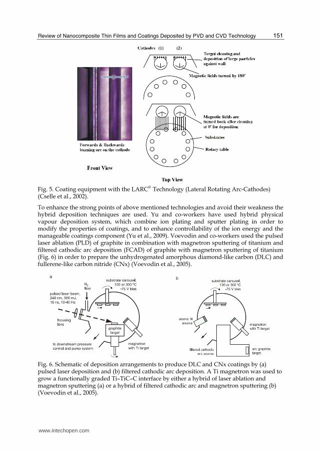
production is the LARC Technology (Fig. 5). The most important advantages on the
LARC Technology come from the rotating cathodes and their lateral position. The cathodes are in permanent rotation; the magnetic field is generated by coils and permanent magnets controlled both vertically and radially (Cselle et al., 2002; Koch et al., 2007).
www.intechopen.com
Review of Nanocomposite Thin Films and Coatings Deposited by PVD and CVD Technology
151
Fig. 5. Coating equipment with the LARC Technology (Lateral Rotating Arc-Cathodes) (Cselle et al., 2002).
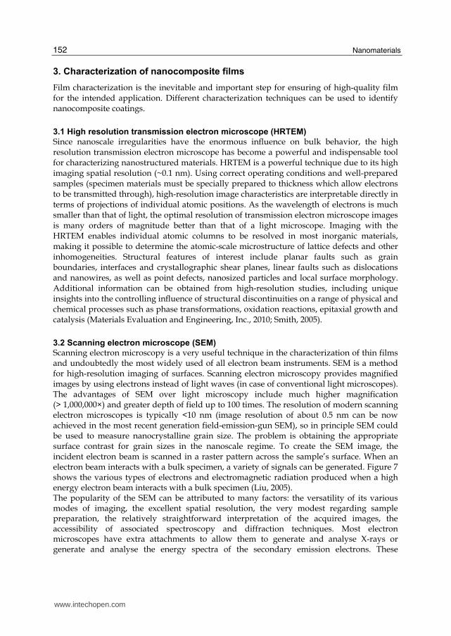
To enhance the strong points of above mentioned technologies and avoid their weakness the hybrid deposition techniques are used. Yu and co-workers have used hybrid physical vapour deposition system, which combine ion plating and sputter plating in order to modify the properties of coatings, and to enhance controllability of the ion energy and the manageable coatings component (Yu et al., 2009). Voevodin and co-workers used the pulsed laser ablation (PLD) of graphite in combination with magnetron sputtering of titanium and filtered cathodic arc deposition (FCAD) of graphite with magnetron sputtering of titanium (Fig. 6) in order to prepare the unhydrogenated amorphous diamond-like carbon (DLC) and fullerene-like carbon nitride (CNx) (Voevodin et al., 2005).
Fig. 6. Schematic of deposition arrangements to produce DLC and CNx coatings by (a) pulsed laser deposition and (b) filtered cathodic arc deposition. A Ti magnetron was used to grow a functionally graded Ti–TiC–C interface by either a hybrid of laser ablation and magnetron sputtering (a) or a hybrid of filtered cathodic arc and magnetron sputtering (b) (Voevodin et al., 2005).
www.intechopen.com
Nanomaterials
152
3. Characterization of nanocomposite films
Film characterization is the inevitable and important step for ensuring of high-quality film for the intended application. Different characterization techniques can be used to identify nanocomposite coatings.
3.1 High resolution transmission electron microscope (HRTEM)
Since nanoscale irregularities have the enormous influence on bulk behavior, the high resolution transmission electron microscope has become a powerful and indispensable tool for characterizing nanostructured materials. HRTEM is a powerful technique due to its high imaging spatial resolution (~0.1 nm). Using correct operating conditions and well-prepared samples (specimen materials must be specially prepared to thickness which allow electrons to be transmitted through), high-resolution image characteristics are interpretable directly in terms of projections of individual atomic positions. As the wavelength of electrons is much smaller than that of light, the optimal resolution of transmission electron microscope images is many orders of magnitude better than that of a light microscope. Imaging with the HRTEM enables individual atomic columns to be resolved in most inorganic materials, making it possible to determine the atomic-scale microstructure of lattice defects and other inhomogeneities. Structural features of interest include planar faults such as grain boundaries, interfaces and crystallographic shear planes, linear faults such as dislocations and nanowires, as well as point defects, nanosized particles and local surface morphology. Additional information can be obtained from high-resolution studies, including unique insights into the controlling influence of structural discontinuities on a range of physical and chemical processes such as phase transformations, oxidation reactions, epitaxial growth and catalysis (Materials Evaluation and Engineering, Inc., 2010; Smith, 2005).
3.2 Scanning electron microscope (SEM)
Scanning electron microscopy is a very useful technique in the characterization of thin films and undoubtedly the most widely used of all electron beam instruments. SEM is a method for high-resolution imaging of surfaces. Scanning electron microscopy provides magnified images by using electrons instead of light waves (in case of conventional light microscopes). The advantages of SEM over light microscopy include much higher magnification (> 1,000,000×) and greater depth of field up to 100 times. The resolution of modern scanning electron microscopes is typically <10 nm (image resolution of about 0.5 nm can be now achieved in the most recent generation field-emission-gun SEM), so in principle SEM could be used to measure nanocrystalline grain size. The problem is obtaining the appropriate surface contrast for grain sizes in the nanoscale regime. To create the SEM image, the incident electron beam is scanned in a raster pattern across the sample’s surface. When an electron beam interacts with a bulk specimen, a variety of signals can be generated. Figure 7 shows the various types of electrons and electromagnetic radiation produced when a high energy electron beam interacts with a bulk specimen (Liu, 2005). The popularity of the SEM can be attributed to many factors: the versatility of its various modes of imaging, the excellent spatial resolution, the very modest regarding sample preparation, the relatively straightforward interpretation of the acquired images, the accessibility of associated spectroscopy and diffraction techniques. Most electron microscopes have extra attachments to allow them to generate and analyse X-rays or generate and analyse the energy spectra of the secondary emission electrons. These
www.intechopen.com

Review of Nanocomposite Thin Films and Coatings Deposited by PVD and CVD Technology
153
attachments create a more powerful tool for the study of qualitative and quantitative chemical analysis, for example X-ray photoelectron spectroscopy (XPS), Auger electron spectroscopy (AES), energy dispersive X-ray emission (EDX), wavelength dispersive X-ray emission (WDX), electron back-scattered diffraction (EBSD) (Smith, 2005).
Fig. 7. Schematic view of the different signals generated after an electron beam interacts with a bulk specimen (Materials Evaluation and Engineering, Inc., 2010).
3.3 X-ray photoelectron spectroscopy (XPS) X-ray photoelectron spectroscopy is the most useful analysis technique used to obtain chemical information about different elements at sample surfaces. In XPS the sample is placed in a high vacuum environment and the beam of low-energy X-rays (or electron) irradiates the sample and produce photo-ionisation. The energy of the ejected photoelectrons is a function of its binding energy (which is the energy required to remove the electron from its atom) and is characteristic of the element from which it was emitted. The equation which describes the energy of the photo-ionisation process is:
EB=hυ- EK-W (2)
where EB is binding energy of the electron from a particular energy level, hυ is the incident X-ray photon (or electron) energy, EK is the kinetic energy of the ejected photoelectron, W is the spectrometer work function (Clarke & Eberhardt, 2002). From the binding energy we can obtain some important information about the samples (Fig. 8) under investigation: the relative quantity of each element, the elements from which it is made, the chemical state of the elements present, depth distribution (Zhang, 2007).
Fig. 8. Typical XPS core-level spectra of (a) Si 2p and (b) N 1s from several Ti–Si–N films (Jiang et al., 2004).
www.intechopen.com
Nanomaterials
154
3.4 Auger electron spectroscopy (AES)
Auger electron spectroscopy provides information about the chemical composition of the outermost material comprising a solid surface or interface. The principal advantages of AES over other surface analysis methods are excellent spatial resolution, surface sensitivity (~20 Ǻ), and detection of light elements (Materials Evaluation and Engineering, Inc., 2010). Different penetrations and accuracies of selected compositions analysis method presents Table 2.
Analysis method
Elemental range
Detection limits (at. %)
Spatial resolution
Penetration
XPS Li-U 0.1÷1 100 µm 1.5 nm
AES Li-U 0.5 10 nm 0.5÷7.5 nm
RBS Li-U 1.0 1÷4 mm 2÷30 nm
EDX Be-U 0.1 0.5÷2.0 µm 1÷3 µm
Table 2. Composition analysis methods (Zhang, 2007).
3.5 Raman spectroscopy
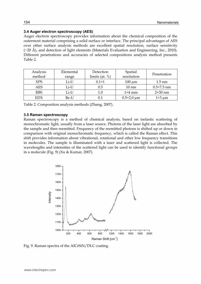
Raman spectroscopy is a method of chemical analysis, based on inelastic scattering of monochromatic light, usually from a laser source. Photons of the laser light are absorbed by the sample and then reemitted. Frequency of the reemitted photons is shifted up or down in comparison with original monochromatic frequency, which is called the Raman effect. This shift provides information about vibrational, rotational and other low frequency transitions in molecules. The sample is illuminated with a laser and scattered light is collected. The wavelengths and intensities of the scattered light can be used to identify functional groups in a molecule (Fig. 9) (Xu & Kumar, 2007).
200 400 600 800 1200 1400 1600 1800 2000
1000
1100
1200
1300
1400
1500
1600
1700
1800
Inte
nsity
Raman Shift [cm-1]
Fig. 9. Raman spectra of the AlCrSiN/DLC coating.
www.intechopen.com
Review of Nanocomposite Thin Films and Coatings Deposited by PVD and CVD Technology
155
3.6 Grain size
In most studies of the grain size of nanocrystalline materials X-ray line-broadening analysis or direct measurements by transmission electron microscopy are performed. To estimate the grain size, the well-known Scherrer formula is used by measuring the full width at half maximum (FWHM) of the XRD diffraction peak:
cos
Kd (3)
where d is crystallite size, K is the shape factor, is the wavelength of the X-rays , is the
full width at half-maximum XRD peak in radians, and is the position of the peak maximum. The Scherrer equation is limited to nano-scale particles. It is not applicable to grains larger than about 100 nm. Otherwise, other methods, in particular transmission electron microscopy, must be used (Koch et al., 2007).
3.7 Atomic force microscopy (AFM)
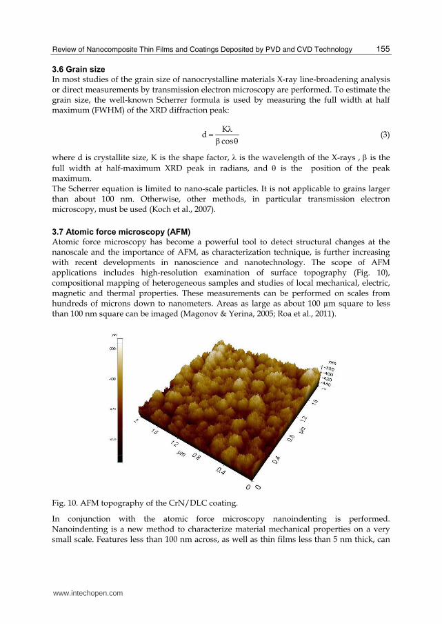
Atomic force microscopy has become a powerful tool to detect structural changes at the nanoscale and the importance of AFM, as characterization technique, is further increasing with recent developments in nanoscience and nanotechnology. The scope of AFM applications includes high-resolution examination of surface topography (Fig. 10), compositional mapping of heterogeneous samples and studies of local mechanical, electric, magnetic and thermal properties. These measurements can be performed on scales from hundreds of microns down to nanometers. Areas as large as about 100 µm square to less than 100 nm square can be imaged (Magonov & Yerina, 2005; Roa et al., 2011).
Fig. 10. AFM topography of the CrN/DLC coating.
In conjunction with the atomic force microscopy nanoindenting is performed. Nanoindenting is a new method to characterize material mechanical properties on a very small scale. Features less than 100 nm across, as well as thin films less than 5 nm thick, can
www.intechopen.com
Nanomaterials
156
be evaluated. Test methods include indentation for comparative and quantitative hardness determination and scratching for evaluation of wear resistance and thin film adhesion. Indentation forces ranging from 1 µN to 100 mN can be made to measure material hardness (Materials Evaluation and Engineering, Inc., 2010).
4. Applications of nanocomposite films
Since the introduction in 1993 of nc-Ti1-xAlxN/a-Si3N4 nanocomposite coatings for
machining applications, such as steel turning, drilling and milling (Holubar et al., 2000),
many new nanocomposite coatings have been developed in order to increase the machining
speed, the lifetime of the coated tools and improve the quality of the machined surface.
Due to high hardness and wear resistance nanocomposite coatings show excellent results
even at normal cutting conditions. The high hardness of the nanocomposite coatings can be
maintained at high temperatures. The enormous hardness will be extremely important for
dry cutting and for machining with minimum quantity lubrication.
Modern nanostructured coatings for structural and functional applications, are used mainly
for wear protection of machining tools and for the reduction of friction in sliding parts. The
nanocomposite coatings find increasing number of applications also on tools for forming,
e.g. extrusion, stamping, etc. The demands on the tool material of an extrusion die are high
hardness, creep resistance, yield strength, toughness at elevated temperatures, wear and
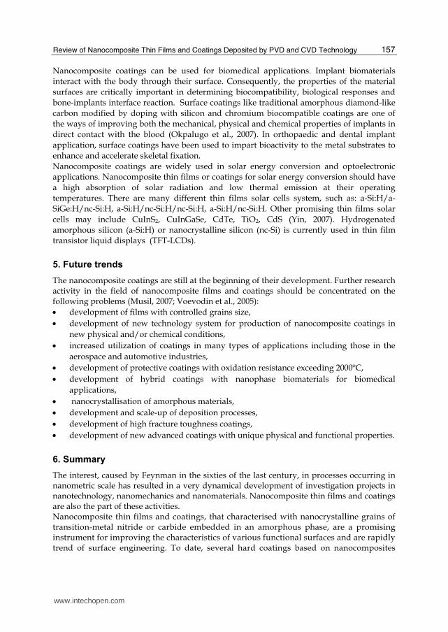
corrosion resistance. It should be suitable for surface coatings. Hard coating, such as nc-
AlCrN/a-Si3N4, nc-AlTiN/a-Si3N4 deposited by physical vapour deposition on extrusion
dies have been used in order to increase their life time and properties (Fig. 11) (Faga et al.,
2007; Veprek & Veprek-Heijman, 2008).
Fig. 11. The performance of uncoated and coated tool for folding boxes for cigarettes (Veprek & Veprek-Heijman, 2008).
An important advantage of the nc-TiN/a-Si3N4, nc-AlTiN/ a-Si3N4, and nc-AlCrN/ a-Si3N4
nanocomposites coatings is their high thermal stability and high oxidation resistance up to
temperatures of more than 800ºC (Veprek & Veprek-Heijman, 2008).
www.intechopen.com
Review of Nanocomposite Thin Films and Coatings Deposited by PVD and CVD Technology
157
Nanocomposite coatings can be used for biomedical applications. Implant biomaterials
interact with the body through their surface. Consequently, the properties of the material
surfaces are critically important in determining biocompatibility, biological responses and
bone-implants interface reaction. Surface coatings like traditional amorphous diamond-like
carbon modified by doping with silicon and chromium biocompatible coatings are one of
the ways of improving both the mechanical, physical and chemical properties of implants in
direct contact with the blood (Okpalugo et al., 2007). In orthopaedic and dental implant
application, surface coatings have been used to impart bioactivity to the metal substrates to
enhance and accelerate skeletal fixation.
Nanocomposite coatings are widely used in solar energy conversion and optoelectronic
applications. Nanocomposite thin films or coatings for solar energy conversion should have
a high absorption of solar radiation and low thermal emission at their operating
temperatures. There are many different thin films solar cells system, such as: a-Si:H/a-
SiGe:H/nc-Si:H, a-Si:H/nc-Si:H/nc-Si:H, a-Si:H/nc-Si:H. Other promising thin films solar
cells may include CuInS2, CuInGaSe, CdTe, TiO2, CdS (Yin, 2007). Hydrogenated
amorphous silicon (a-Si:H) or nanocrystalline silicon (nc-Si) is currently used in thin film
transistor liquid displays (TFT-LCDs).
5. Future trends
The nanocomposite coatings are still at the beginning of their development. Further research activity in the field of nanocomposite films and coatings should be concentrated on the following problems (Musil, 2007; Voevodin et al., 2005):
development of films with controlled grains size,
development of new technology system for production of nanocomposite coatings in
new physical and/or chemical conditions,
increased utilization of coatings in many types of applications including those in the
aerospace and automotive industries,
development of protective coatings with oxidation resistance exceeding 2000ºC,
development of hybrid coatings with nanophase biomaterials for biomedical
applications,
nanocrystallisation of amorphous materials,
development and scale-up of deposition processes,
development of high fracture toughness coatings,
development of new advanced coatings with unique physical and functional properties.
6. Summary
The interest, caused by Feynman in the sixties of the last century, in processes occurring in nanometric scale has resulted in a very dynamical development of investigation projects in nanotechnology, nanomechanics and nanomaterials. Nanocomposite thin films and coatings are also the part of these activities. Nanocomposite thin films and coatings, that characterised with nanocrystalline grains of transition-metal nitride or carbide embedded in an amorphous phase, are a promising instrument for improving the characteristics of various functional surfaces and are rapidly trend of surface engineering. To date, several hard coatings based on nanocomposites
www.intechopen.com
Nanomaterials
158
have been successfully developed and commercialized for engineering applications. There are many possible future applications of nanocomposite thin films and coatings. Further improvement of the presently available and newly developed nanocomposite coatings will push the technology towards new horizons. Several techniques, in particular PVD and CVD are now available for the deposition of nanocomposite films on various kinds of substrates. Despite the big number of scientific investigations in the field of nanocomposite thin films and coatings, with results published in professional and competent literature, still some lack and deficiency of verified material knowledge occurs.
7. Acknowledgment
The research was partially financed within the framework of the Polish State Committee for Scientific Research Project No N N507 550738 headed by Dr Krzysztof Lukaszkowicz.
8. References
Audronis M.; Leyland A.; Kelly P.J. & Mathews A. (2008). Composition and structure-
property relationships of chromium-diboride / molybdenum-disulhipe PVD
nanocomposite hard coatings deposited by pulsed magnetron sputtering. Applied
Physics A, vol. 91, (April 2008), pp. 77-86, ISSN 0947-8396.
Cheng, Y.C.; Browne, T.; Heckerman, B. & Meletis, E.I. (2010). Mechanical and tribological
properties of nanocomposite TiSiN coatings. Surface and Coatings Technology, vol.
204, (April 2010), pp. 2123-2129, ISSN 0257-8972.
Clarke, A.R. & Eberhardt, C.N (2002). Microscopy techniques for materials science, Woodhead
Publishing Limited, ISBN 1-85573-587-3, Cambridge, England.
Cselle, T.; Morstein, M.; Holubar, P.; Jilek, M. & Karimi A. (2002). Nanostructured
coatings and processes on an industrial scale, Proceedings of the Gorham 2002
Conference – Advanced Coatings and Surface Systems for Cutting Tools and Wear Parts,
pp. 1-17, Atlanta, Georgia, USA, November 18-20, 2002.
Dobrzanski, L.A.; Lukaszkowicz, K.; Zarychta, A. & Cunha, L. (2005). Corrosion resistance
of multilayer coatings deposited by PVD techniques onto the brass substrate.
Journal of Materials Processing Technology, vol. 164-165, (May 2005), pp. 816-821,
ISSN 0924-0136.
Donnet, C. & Erdemir, A. (2004). Solid lubricant coatings: recent developments and future
trends. Tribology Letters, vol. 17, No. 3, (October 2004), pp. 389-397, ISSN 1023-
8883.
Faga, M.G.; Gauiter, G.; Calzavarini, R.; Perucca, M.; Aimo Boot, E.; Cartasegna, F. &
Settineri, L. (2007). Advantages of nanocomposite coatings deposited by high
power pulse magnetron sputtering technology. Wear, vol. 263 (September 2007),
pp. 1306-1314, ISSN 0043-1648.
Holubar, P.; Jilek, M. & Sima, M. (2000). Present and possible future applications of
superhard nanocomposite coatings. Surface and Coatings Technology, vol. 133-134,
(November 2000), pp. 145-151, ISSN 0257-8972.
www.intechopen.com
Review of Nanocomposite Thin Films and Coatings Deposited by PVD and CVD Technology
159
Jiang, N., Shen, Y.G., Mai, Y.W., Chan, T. & Tung, S.C. (2004). Nanocomposite Ti-Si-N
films deposited by reactive unbalanced magnetron sputtering at room
temperature. Materials Science and Engineering B, vol. 106, (January 2004), pp. 163-
171, ISSN 0921-5107.
Koch, C.C.; Ovid`ko, I.A.; Seal, S. & Veprek, S. (2007). Structural Nanocrystalline Materials.
Fundamental and Applications, Cambridge University Press, ISBN-13 978-521-
85565, Cambridge, UK.
Liu, J. (2005). High-Resolution Scanning Electron Microscopy, In: Handbook of microscopy
for nanotechnology, N. Yao & Z.L. Wang (EDS.), 325-360, Kluwer Academic
Publisher, ISBN 1-4020-8003-4, Boston/Dordrecht/New York/London.
Lukaszkowicz, K. & Dobrzanski, L.A. (2008). Structure and mechanical properties of
gradient coatings deposited by PVD technology onto X40CrMoV5-1 steel
substrate. Journal of Materials Science, vol. 43, (May 2008), pp. 3400-3407, ISSN
0022-2461.
Lukaszkowicz, K.; Sondor, J.; Kriz, A. & Pancielejko, M. (2010). Structure, mechanical
properties and corrosion resistance of nanocomposite coatings deposited by PVD
technology onto the X6CrNiMoTi17-12-2 and X40CrMoV5-1 steel substrates.
Journal of Materials Science, vol. 45, (March 2010), pp. 1629-1637, ISSN 0022-2461.
Magonov, S.N. & Yerina, N.A. (2005). Visualization of Nanostructures with Atomic Force
Microscopy, In: Handbook of microscopy for nanotechnology, N. Yao & Z.L. Wang
(EDS.), 427-454, Kluwer Academic Publisher, ISBN 1-4020-8003-4,
Boston/Dordrecht/New York/London.
Materials Evaluation and Engineering, Inc. (2010). Scanning Electron Microscopy, In:
Handbook of analytical Methods for Materials, Plymouth, MN 55441-5447, USA,
Available from http://www.mee-inc.com
Moore, J.J.; Park, I.-W. & Lin, J. (2007). Nanostructured, multifunctional tribological
coatings, In: Nanocomposite Thin Films and Coatings, S. Zhang & N. Ali (Eds.), 329-
379, Imperial College Press, ISBN-13 978-1-86094-784-1, London, UK.
Musil, J. (2007). Properties of hard nanocomposite thin films, In: Nanocomposite Thin Films
and Coatings, S. Zhang & N. Ali (Eds.), 281-328, Imperial College Press, ISBN-
13 978-1-86094-784-1, London, UK.
Okpalugo, T.I.T.; Ali, N.; Ogwu, A.A.; Kousar, Y. & Ahmed, W. (2007). Amorphous and
nanocomposite diamond-like carbon coatings for biomedical applications, In:
Nanocomposite Thin Films and Coatings, S. Zhang & N. Ali (Eds.), 513-572, Imperial
College Press, ISBN-13 978-1-86094-784-1, London, UK.
Park, I.W.; Choi, S.R.; Lee, M.H. & Kim, K.H. (2003). Effects of Si addition on the
microstructural evolution and hardness of Ti-Al-Si-N films prepared by the
hybrid system ion plating and sputtering techniques. Journal of Vacuum Science &
Technology A: Vacuum, Surface, and Films, vol. 21, No. 4, (July 2003), pp 895-899,
ISSN 0734-2101.
Polychronopoulou, K.; Baker, M.A.; Rebholz, C.; Neidhardt, J.; O`Sullivan, M.; Reiter, A.E.; Kanakis, K.; Leyland, A.; Matthews, A. & Mitterer, C. (2009). The nanostructure, wear and corrosion performance of arc-evaporated CrBxNy nanocomposite
www.intechopen.com
Nanomaterials
160
coatings. Surface and Coatings Technology, vol. 204, (October 2009), pp. 246-255, ISSN 0257-8972.
Rafaja, D.; Poklad, A.; Klemm, V.; Schreiber, G.; Heger, D.; Sima, M. & Dopita, M. (2006).
Some consequence of the partial crysrallographic coherence between
nanocrystalline domains in Ti-Al-N and Ti-Al-Si-N coatings. Thin Solid Films, vol.
514, (August 2006), pp. 240-249, ISSN 0040-6090.
Roa, J.J.; Oncins, G.; Diaz, J.; Capdevila, X.G.; Sanz, F. & Segarra, M. (2011). Study of the
friction, adhesion and mechanical properties of single crystals, ceramics and
ceramic coatings by AFM. Journal of the European Ceramic Society, vol. 31, (April
2011), pp. 429-449, ISSN 0955-2219.
Smith, D.J. (2005). High-Resolution Transmission Electron Microscopy, In: Handbook of
microscopy for nanotechnology, N. Yao & Z.L. Wang (EDS.), 427-454, Kluwer
Academic Publisher, ISBN 1-4020-8003-4, Boston/Dordrecht/New York/London.
Tjong, S.C. (2007). Properties of chemical vapor deposited nanocrystalline diamond and
nanodiamond/amorphous carbon composite films, In: Nanocomposite Thin Films
and Coatings, S. Zhang & N. Ali (Eds.), 329-379, Imperial College Press, ISBN-
13 978-1-86094-784-1, London, UK.
Tjong, S.S. & Chen, H. (2004). Nanocrystalline materials and coatings. Materials Science and
Engineering R, vol. 45, (September 2004), pp. 1-88, ISSN 0927-796X.
Vaz, F.; Rebouta, L.; Goudeau, P.; Pacaud, J.; Garem, H.; Riviere, J.P.; Cavaleiro, A. &
Alves, E. (2000). Characterisation of Ti1-xSixNy nanocomposite coatings. Surface
and Coatings Technology, vol. 133-134, (November 2000), pp. 307-313, ISSN 0257-
9872.
Veprek, S. & Reiprich, S. (1995). A concept for the design of novel superhard coatings.
Thin Solid Films, vol. 268, (November 1995), pp. 64-71, ISSN 0040-6090.
Veprek, S. & Veprek-Heijman, M.J.G. (2008). Industrial applications of superhard nanocomposite coatings. Surface and Coatings Technology, vol. 202, (July 2008), pp. 5063-5073, ISSN 0257-8972.
Veprek, S. (1997). Conventional and new approaches towards the design of novel
superhard materials. Surface and Coatings Technology, vol. 97, (December 1997),
pp. 15-22, ISNN 0257-8972.
Veprek, S.; Mannling, H.D.; Karvankova, P. & Prochazka, J. (2006). The issue of the
reproducibility of deposition of superhard nanocomposites with hardness of ≥ 50
GPa. Surface and Coatings Technology, vol. 201, (March 2006), pp. 6064-6070, ISSN
0257-8972.
Veprek, S.; Nesladek, P.; Niederhofer, A.; Glatz, F.; Jilek, M. & Sima, M. (1998). Recent progress in the superhard nanocrystalline composites: towards their industralization and understanding of the origin of the superhardness. Surface and Coatings Technology, vol. 108-109, (October 1998), pp. 138-147, ISSN 0257-8972.
Veprek, S.; Niederhofer, A.; Moto, K.; Bolom, T.; Mannling, H.D.; Nesladek, P.; Dollinger, G. & Bergmaier, A. (2000). Composition, nanostructure and origin of the ultrahardness in nc-Tin a-Si3N4 a- and nc-TiSi2 nanocomposites with Hv 80 to 105 GPa. Surface and Coatings Technology, vol. 133-134, (November 2000), pp. 152-159, ISSN 0257-8972.
www.intechopen.com
Review of Nanocomposite Thin Films and Coatings Deposited by PVD and CVD Technology
161
Voevodin, A.A. & Zabinski, J.S. (2000). Supertough wear-resistant coatings with ‘chameleon’ surface adaptation. Thin Solid Films, vol. 370, (July 2000), pp. 223-231, ISSN 0040-6090.
Voevodin, A.A. & Zabinski, J.S. (2005). Nanocomposite and nanostructured tribological
materials for space applications. Composites Science and Technology, vol. 65, (April
2005), pp. 741-748, ISSN 0266-3538.
Voevodin, A.A.; Hu, J.J. & Zabinski, J.S. (2001). Tribological properties of adaptive
nanocomposite coatings made of yttria stabilized zirconia and gold. Surface and
Coatings Technology, vol. 146-147, (September-October 2001), pp. 351-356, ISSN
0257-8972.
Voevodin, A.A.; Jones, J.G.; Back, T.C.; Zabinski, J.S.; Strel`nitzki, V.E. & Aksenov, I.I. (2005). Comparative study of wear-resistant DLC and fullerene-like CNx coatings produced by pulsed laser and filtered cathodic arc deposition. Surface and Coatings Technology, vol. 197, (July 2005), pp. 116-125, ISSN 0257-8972.
Voevodin, A.A.; O`Neil, J.P. & Zabinski, J.S. (2002). Tribological performance and tribochemistry of nanocrystalline WC/amorphous diamond-like carbon composites. Journal of Vacuum Science & Technology A, vol. 20, (November-December 2002), pp. 1434-1444, ISSN 0734-2101.
Voevodin, A.A.; Zabinski, J.S. & Muratore, C. (2005). Recent Advances in Hard, Tough,
and Low Friction Nanocomposite Coatings. Tsinghua Science and Technology, vol.
10, No. 6, (December 2005), pp. 665-679, ISSN 1007-0214.
Xu, Z. & Kumar, A. (2007). Synthesis, Characterization and Applications of
Nanocrystalline Diamond Films, In: Nanocomposite Thin Films and Coatings, S.
Zhang & N. Ali (Eds.), 207-279, Imperial College Press, ISBN-13 978-1-86094-784-
1, London, UK.
Yin, Y. (2007). Nanocomposite thin films for solar energy conversion, In: Nanocomposite
Thin Films and Coatings, S. Zhang & N. Ali (Eds.), 381-417, Imperial College Press,
ISBN-13 978-1-86094-784-1, London, UK.
Yu, D.; Wang, C.; Cheng, X. & Zhang, F. (2009). Microstructure and properties of TiAlSiN
coatings prepared by hybrid PVD technology. Thin Solid Films, vol. 517, (July
2009), pp. 4950-4955, ISSN 0040-6090.
Zabinski, J.S.; Donley, M.S. & McDevit, N.T. (1993). Mechanistic study of the synergism
between Sb2O3 and MoS2 lubricant system using Raman spectroscopy. Wear, vol.
165, (January 1993), pp. 103-108, ISSN 0043-1648.
Zabinski, J.S.; Donley, M.S.; Dyhouse, V.J. & McDevit, N.T. (1992). Chemical and tribological characterization of PbO-MoS2 films grown by pulsed laser deposition. Thin Solid Films, vol. 214, (March-April 1992), pp. 156-163, ISSN 0040-6090.
Zhang, R.F.; Veprek, S. (2006). On the spinodal nature of the phase segregation and
formation of stable nanostructure in the Ti-Si-N system. Materials Science and
Engineering A, vol. 424 (May 2006), pp. 128-137, ISSN 0921-5093.
Zhang, S.; Sun, D. & Bui, X.L. (2007). Magnetron Sputtered Hard and Yet Tough
Nanocomposite Coatings with Case Studies: Nanocrystalline TiN Embedded in
Amorphous SiNX, In: Nanocomposite Thin Films and Coatings, S. Zhang & N. Ali
(Eds.), 1-110, Imperial College Press, ISBN-13 978-1-86094-784-1, London, UK.
www.intechopen.com
Nanomaterials
162
Zou, C.W.; Wang, H.J.; Li, M.; Yu, J.F.; Liu, C.S.; Guo, L.P. & Fu, D.J. (2010). Characterization and properties of TiN-containing amorphous Ti-Si-N nanocomposite coatings prepared by arc assisted middle frequency magnetron sputtering. Vacuum, vol. 84, (February 2010), pp. 817-822, ISSN 0042-207X.
www.intechopen.com
NanomaterialsEdited by Prof. Mohammed Rahman
ISBN 978-953-307-913-4Hard cover, 346 pagesPublisher InTechPublished online 22, December, 2011Published in print edition December, 2011
InTech EuropeUniversity Campus STeP Ri Slavka Krautzeka 83/A 51000 Rijeka, Croatia Phone: +385 (51) 770 447 Fax: +385 (51) 686 166www.intechopen.com
InTech ChinaUnit 405, Office Block, Hotel Equatorial Shanghai No.65, Yan An Road (West), Shanghai, 200040, China
Phone: +86-21-62489820 Fax: +86-21-62489821
The book "Nanomaterials" includes all aspects of metal-oxide nano-structures, nano-composites, and polymermaterials instigating with materials survey and preparations, growth and characterizations, processing andfabrications, developments and potential applications. These topics have utilized innovative methods ofpreparation, improvement, and continuous changes in multidimensional ways. The innovative frontiers arebranching out from time to time to advanced nanotechnology. It is an important booklet for scientificorganizations, governmental research-centers, academic libraries, and the overall research and developmentof nano-materials in general. It has been created for widespread audience with diverse backgrounds andeducation.
How to referenceIn order to correctly reference this scholarly work, feel free to copy and paste the following:
Krzysztof Lukaszkowicz (2011). Review of Nanocomposite Thin Films and Coatings Deposited by PVD andCVD Technology, Nanomaterials, Prof. Mohammed Rahman (Ed.), ISBN: 978-953-307-913-4, InTech,Available from: http://www.intechopen.com/books/nanomaterials/review-of-nanocomposite-thin-films-and-coatings-deposited-by-pvd-and-cvd-technology