air force t.o. 31w2-2gsc24-2 army tm 11-5805-688-14-1 …
TRANSCRIPT

AIR FORCE T.O. 31W2-2GSC24-2ARMY TM 11-5805-688-14-1
NAVY NAVELEX 0967-LP-545-3010
TECHNICAL MANUAL
SERVICE AND MAINTENANCE INSTRUCTIONS
AN/GSC-24( V) MULTIPLEXER SET
MARTIN MARIETTA AEROSPACEORLANDO DIVISION
COMMUNICATIONS AND ELECTRONICS
Contract NumberF30602-75-C-0009
This is a reprint which includes currentpages from Changes 1 and 2.
Published under authority of the Secretary of the Air Force,under authority of the Secretary of the Army, and by directionof Commander, Naval Electronics Systems Command.
1 JANUARY 1976

T.O. 31W2-2GSC24-2TM 11-5805-688-14-1
NAVELEX 0967-LP-545-3010
LIST OF EFFECTIVE PAGES
Insert latest changed pages; dispose of superseded pages in accordance with applicable regulations.
NOTE: On a changed page, the portion of the text affected by the latest change is indicated by a vertical line, or otherchange symbol, in the outer margin of the page. Changes to illustrations are indicated miniature pointing hands. Changesto wiring diagrams are indicated by shaded areas.
Total number of pages in this manual is 388 consisting of the following:
Page #Change Page #ChangeNo. No. No. No.
Title................................................................ 0 FO-13 ............................................................. 0A .................................................................... 0 FO-14 Blank ................................................... 0i - xii ............................................................... 0 FO-15 ............................................................. 01-1 - 1-16....................................................... 0 FO-16 Blank ................................................... 02-1 - 2-5 ........................................................ 0 FO-17............................................................. 02-6 Blank ....................................................... 0 FO-18 Blank ................................................... 03-1 - 3-58....................................................... 0 FO-19 ............................................................. 04-1 - 4-4 ......................................................... 0 FO-20 Blank ................................................... 05-1 - 5-177..................................................... 0 FO-21 ............................................................. 05-178 Blank ................................................... 0 FO-22 Blank ................................................... 06-1 - 6-64....................................................... 0Glossary 1 - Glossary 2................................. 0CRI-1 - CRI-7 ................................................ 0CRI-8 Blank ................................................... 0Index 1 - Index 15.......................................... 0Index 16 Blank............................................... 0FO-1 .............................................................. 0FO-2 Blank .................................................... 0FO-3 .............................................................. 0FO-4 Blank .................................................... 0FO-5 .............................................................. 0FO-6 Blank .................................................... 0FO-7 .............................................................. 0FO-8 Blank .................................................... 0FO-9 .............................................................. 0FO-11 ............................................................ 0FO-10 Blank .................................................. 0FO-11 Blank .................................................. 0FO-12 Blank .................................................. 0
# Zero in this column indicates an original page.
A

AIR FORCE T.O. 31W2-2GSC24-2ARMY TM 11-5805-688-14-1
NAVY NAVELEX 0967-LP-545-3010
TECHNICAL MANUAL
SERVICE AND MAINTENANCE INSTRUCTIONS
AN/GSC-24( V) MULTIPLEXER SET
MARTIN MARIETTA AEROSPACEORLANDO DIVISION
COMMUNICATIONS AND ELECTRONICS
Contract NumberF30602-75-C-0009
This is a reprint which includes currentpages from Changes 1 and 2.
Published under authority of the Secretary of the AirForce, under authority of the Secretary of the Army, andby direction of Commander, Naval Electronics SystemsCommand.
1 JANUARY 1976

T.O. 31W2-2GSC24-2TM 11-5805-688-14-1
NAVELEX 097-LP-545-3010
LIST OF EFFECTIVE PAGES
Insert latest changed pages; dispose of superseded pages in accordance with applicable regulations.
NOTE: On a changed page, the portion of the text affected by the latest change is indicated by a vertical line, or otherchange symbol, in the outer margin of the page. Changes to illustrations are indicated by miniature pointing hands.Changes to wiring diagrams are indicated by shaded areas.
Total number of pages in this manual is 392 consisting of the following:
Page #Change Page #ChangeNo. No. No. No.
Title................................................................ 2 3-60 Blank ...................................................... 1A - B............................................................... 2 4-1 - 4-4.......................................................... 0C Blank.......................................................... 2 5-1 - 5-4.......................................................... 0i...................................................................... 0 5-5 - 5-6.......................................................... 1ii ..................................................................... 1 5-7 .................................................................. 0iii - v ............................................................... 0 5-8 .................................................................. 2vi - vii ............................................................. 2 5-9 - 5-12........................................................ 0viii - ix............................................................. 0 5-13 - 5-16...................................................... 1x..................................................................... 2 5-17 ................................................................ 0xi - xii ............................................................. 0 5-18 ................................................................ 11-1 - 1-13....................................................... 0 5-19 - 5-20...................................................... 01-14 - 1-16..................................................... 2 5-21 ................................................................ 12-1 - 2-4 ......................................................... 0 5-22 ................................................................ 02-5 ................................................................. 1 5-23 - 5-24...................................................... 12-6 Blank ....................................................... 0 5-25 - 5-38...................................................... 03-1 - 3-2 ......................................................... 0 5-39 ................................................................ 23-3 ................................................................. 2 5-40 ................................................................ 03-4 - 3-6 ......................................................... 0 5-41 - 5-42...................................................... 13-7 ................................................................. 2 5-43 - 5-48...................................................... 03-8 ................................................................. 0 5-49 ................................................................ 23-9 ................................................................. 2 5-50 - 5-59...................................................... 03-10 - 3-16..................................................... 0 5-60 - 6-61...................................................... 23-17 ............................................................... 2 5-62 - 5-65...................................................... 03-18 - 3-38..................................................... 0 5-66 ................................................................ 13-39 ............................................................... 2 5-67 ................................................................ 23-40 - 3-46..................................................... 0 5-68 - 5-84...................................................... 03-47 ............................................................... 2 5-85 - 5-86...................................................... 13-48 - 3-54..................................................... 0 5-87 - 5-98...................................................... 03-55 - 3-56..................................................... 1 5-99 - 5-100.................................................... 13-57 ............................................................... 0 5-101 - 5-104.................................................. 03-58 - 3-59..................................................... 1 5-105 - 5-107.................................................. 1
# Zero in this column indicates an original page.
Change 2 A

T.O. 31W2-2GSC24-2TM 11-5805-688-14-1
NAVELEX 0967-LP-545-3010
Page #Change Page #ChangeNo. No. No. No.
5-108 ............................................................ 0 CRI-1 - CRI-3 ................................................ 05-109 - 5-110................................................. 1 CRI-4.............................................................. 25-111 - 5-112................................................. 0 CRI-5 - CRI-7 ................................................. 05-113 ............................................................ 1 CR8 Blank ...................................................... 05-114 - 5-126................................................. 0 Index 1 ........................................................... 05-127 - 5-128................................................. 1 Index 2 ........................................................... 25-129 - 5-130................................................. 0 Index 3 ........................................................... 05-131 ............................................................. 1 Index 4 ........................................................... 25-132 - 5-136................................................. 0 Index 5 - Index 8 ............................................ 05-137 - 5-138................................................. 1 Index 9 - Index 10 .......................................... 25-139 - 5-145 ................................................ 0 Index 11 ......................................................... 05-146 - 5-148................................................. 1 Index 12 ......................................................... 25-149 - 5-166................................................. 0 Index 13 - Index 15 ........................................ 05-167 - 5-170................................................. 2 Index 16 Blank ............................................... 05-171 - 5-172................................................. 0 FO-1 .............................................................. 15-173 - 5-175................................................. 2 FO-2 Blank .................................................... 05-176 - 5-177 ................................................ 0 FO-3 ............................................................... 06-1 - 6-2 ......................................................... 2 F-4 Blank........................................................ 06-3 - 6-5 ........................................................ 0 FO-5 ............................................................... 16-6 ................................................................ 1 FO-6 Blank ..................................................... 06-7 - 6-10....................................................... 0 FO-7 ............................................................... 06-11 - 6-17..................................................... 2 FO-8 Blank ..................................................... O6-18- 6-21...................................................... 0 F-9.................................................................. 06-22 ............................................................... 1 FO-10 Blank ................................................... 06-23 - 6-41 .................................................... 0 FO-11 ............................................................. 06-42 - 6-45..................................................... 2 FO-12 Blank ................................................... 06-46 - 6-48 Deleted........................................ 2 FO-13 ............................................................. 16-49 ............................................................... 2 FO-14 Blank ................................................... 06-50 Deleted.................................................. 2 FO-15 ............................................................. 16-51 - 6-53..................................................... 0 FO-16 Blank ................................................... 06-54 ............................................................... 2 FO-17 ............................................................. 06-55 - 6-58 Deleted........................................ 2 FO-18 Blank ................................................... 06-59 - 6-60..................................................... 0 FO-19 ............................................................. 06-61 ............................................................... 2 FO-20 Blank ................................................... 06-62 Deleted ................................................. 2 F-21................................................................ 06-63 .............................................................. 0 FC-22 Blank ................................................... 06-64 .............................................................. 2Glossary 1 - Glossary 2 ................................ 0
# Zero in this column indicates an original page.
Change 2 B/(C Blank)

T.O. 31W2-2GSC24-2TM 11-5805-688-14-1
NAVELEX 0967-LP-545- 3011
TABLE OF CONTENTS
Page
LIST OF ILLUSTRATIONS..................................................................................................................................... viii
LIST OF TABLES ............................................................................................................................................... xi
INTRODUCTION ............................................................................................................................................... xii
CHAPTER 1. GENERAL INFORMATION ................................................................................................... 1-1
1-1. Description and Purpose ....................................................................................................... 1-11-6. Leading Particulars ................................................................................................................ 1-31-8. Capabilities and Limitations ................................................................................................... 1-3
1-10. Equipment Supplied............................................................................................................... 1-31-12. Related Technical Manuals. .................................................................................................. 1-31-14. Special Tools ......................................................................................................................... 1-31-16. Test Equipment...................................................................................................................... 1-3
CHAPTER 2. INSTALLATION ..................................................................................................................... 2-1
Section I. INSTALLATION LOGISTICS ................................................................................................. 2-1
2-1. General .................................................................................................................................. 2-12-3. Unloading and Unpacking...................................................................................................... 2-12-5. Storage Housing Requirements............................................................................................. 2-12-7. Receiving Data....................................................................................................................... 2-22-9. Installation Housing Requirements ........................................................................................ 2-2
Section II. INSTALLATION PROCEDURES........................................................................................... 2-3
2-11. General .................................................................................................................................. 2-32-13. Installation Procedures .......................................................................................................... 2-4
CHAPTER 3. PREPARATION FOR USE .................................................................................................... 3-1
Section I. GENERAL.............................................................................................................................. 3-1
3-1. Introduction ............................................................................................................................ 3-13-5. Typical System Applications .................................................................................................. 3-1
3-11. Channel and Port Relationships ............................................................................................ 3-33-17. Channel Rates and Forms..................................................................................................... 3-53-19. Digital Data With Associated Timing ..................................................................................... 3-53-22. Digital Data Without Associated Timing ................................................................................ 3-63-25. Voice Data ............................................................................................................................. 3-73-27. Channel Card Options ........................................................................................................... 3-7
i

T.O. 31W2-2GSC24-2TM 11-5805-688-14-1
NAVELEX 0967-LP-545- 3011
TABLE OF CONTENTS (CONT)
Page
Section II. PREPARATION OF CONFIGURATION WORKSHEETS ..................................................... 3-8
3-29. General. ................................................................................................................................. 3-83-32. Multiplexer Channel Electronics............................................................................................. 3-93-36. Multiplexer Common Electronics ........................................................................................... 3-123-41. Demultiplexer Channel Electronics........................................................................................ 3-193-43. Demultiplexer Common Electronics ...................................................................................... 3-223-45. Supplemental Configuration Considerations ......................................................................... 3-223-56. Voice Processing Ground Rules............................................................................................ 3-273-58. Special Demultiplexer Output Smoothing Options................................................................. 3-28
Section III. EQUIPMENT PREPARATION PROCEDURES .................................................................... 3-29
3-64. Preparation Considerations ................................................................................................... 3-293-66. Multiplexer Channel Electronics Setup Procedures............................................................... 3-293-68. RCB Card............................................................................................................................... 3-293-70. TE/TR Card............................................................................................................................ 3-353-71. VE Card. ................................................................................................................................ 3-373-72. Multiplexer Common Electronics Setup Procedures. ............................................................ 3-373-74. RT Card. ................................................................................................................................ 3-373-75. OEG Card .............................................................................................................................. 3-413-76. Seq Card................................................................................................................................ 3-413-77. GC/DM Card .......................................................................................................................... 3-453-78. Demultiplexer Channel Electronics Setup Procedures.......................................................... 3-453-80. SB Card ................................................................................................................................. 3-453-81. NBSB Card. ........................................................................................................................... 3-483-82. VD Card ................................................................................................................................ 3-503-83. TD Card. ................................................................................................................................ 3-503-84. Demultiplexer Common Electronics Setup Procedures......................................................... 3-523-86. OEG Card .............................................................................................................................. 3-523-87. Seq Card................................................................................................................................ 3-523-88. GC/DM Card .......................................................................................................................... 3-523-89. FS Card.................................................................................................................................. 3-523-90. ERD Card............................................................................................................................... 3-523-91. Display Card Setup Procedures............................................................................................. 3-533-93. Thermal Alarm Options.......................................................................................................... 3-53
3-96.1. Remote Alarm Options .......................................................................................................... 3-563-97. Multiplexer Set Operational Tests.......................................................................................... 3-56
Section IV. PREPARATION FOR RESHIPMENT.................................................................................... 3-58
3-99. General .................................................................................................................................. 3-583-101. Packing Procedures............................................................................................................... 3-58
CHAPTER 4. OPERATION.......................................................................................................................... 4-1
4-1. Introduction ............................................................................................................................ 4-14-3. Controls and Indicators.......................................................................................................... 4-14-5. Operating Instructions............................................................................................................ 4-14-7. Starting Procedures. .............................................................................................................. 4-1
Change 1 ii

T.O. 31W2-2GSC24-2TM 11-5805-688-14-1
NAVELEX 0967-LP-545-3010
TABLE OF CONTENTS (CONT)
PageCHAPTER 4. (Continued)
4-8. Lamp Test Procedures.................................................................................................... 4-44-9. Self-Test Procedures. ..................................................................................................... 4-4
4-10. Stopping Procedures....................................................................................................... 4-44-11. Emergency Stopping Procedures.................................................................................... 4-4
CHAPTER 5. THEORY OF OPERATION ............................................................................................. 5-1
5-1. Introduction...................................................................................................................... 5-1
Section I. MESSAGE FORMAT AND BASIC EQUIPMENT CONCEPTS ...................................... 5-3
5-5. General............................................................................................................................ 5-25-6. Message Format ............................................................................................................. 5-25-7. Overall Message Format. ................................................................................................ 5-2
5-13. Overhead Message Format ............................................................................................ 5-45-19. Multiplexer Basic Concepts. ............................................................................................ 5-55-20. Introduction...................................................................................................................... 5-55-27. Equipment Application..................................................................................................... 5-65-30. Processing of Asynchronous Inputs................................................................................ 5-85-42. Channel Data Gating Function. ....................................................................................... 5-115-48. Overhead Service Function............................................................................................. 5-145-55. Demultiplexer Basic Concepts. ....................................................................................... 5-165-57. Frame Synchronization Function..................................................................................... 5-165-64. Smoothing Function. ....................................................................................................... 5-18
Section II. MULTIPLEXER, DEMULTIPLEXER, AND OVERALL DIAGNOSTICFUNCTIONAL BLOCK DIAGRAM DISCUSSIONS.................................................. 5-20
5-69. Overall Multiplexer Functional Block Diagram Discussion .............................................. 5-205-70. General............................................................................................................................ 5-205-71. Rate Comparison Buffer (RCB) Card............................................................................. 5-205-76. Transition Encoder/Timing Recovery (TE/TR) Card ...................................................... 5-215-81. Voice Encoder (VE) Card............................................................................................... 5-225-85. Sequencer (Seq) Card. .................................................................................................. 5-235-90. Overhead Enable Generator (OEG) Card. ..................................................................... 5-235-94. Gated Clock/Data Mux (GC/DM) Card............................................................................ 5-24
5-102. Reference Timer (RT) Card ............................................................................................ 5-255-106. Overall Demultiplexer Functional Block Diagram Discussion ........................................ 5-265-107. General............................................................................................................................ 5-265-108. Frame Sync (FS) Card .................................................................................................... 5-265-113. Sequencer (Seq) Card. ................................................................................................... 5-275-116. Overhead Enable Generator (OEG) Card....................................................................... 5-285-119. Gated Clock/Data Mux (GC/DM) Card ........................................................................... 5-285-123. Error Rate Detector (ERD) Card .................................................................................... 5-295-126. Smoothing Buffer (SB) Card ........................................................................................... 5-29
iii

T.O. 31W2-2GSC24-2TM 11-5805-688-14-1
NAVELEX 0967-LP-545-3010
TABLE OF CONTENTS (CONT)
PageSection II. (Continued)
5-130. Narrow Band Smoothing Buffer (NBSB) Card. ............................................................... 5-305-132. Transition Decoder (TD) Card........................................................................................ 5-305-135. Voice Decoder (VD) Card................................................................................................ 5-315-138. Overall Diagnostic Functional Block Diagram ................................................................. 5-315-139. General............................................................................................................................ 5-315-144. System Block Diagram Discussion ................................................................................. 5-325-154. Front Panel Block Diagram Discussion........................................................................... 5-35
Section III. MULTIPLEXER CARDS FUNCTION OPERATION........................................................ 5-38
5-164. Introduction...................................................................................................................... 5-385-166. Rate Comparison Buffer (RCB) Card............................................................................. 5-385-167. General............................................................................................................................ 5-385-168. Block Diagram Discussion. ............................................................................................. 5-395-190. Detailed Circuit Discussion.............................................................................................. 5-465-203. Transition Encoder/Timing Recovery(TE/TR) Card. ....................................................... 5-505-204. General............................................................................................................................ 5-505-205. Block Diagram Discussion .............................................................................................. 5-515-230. Detailed Circuit Discussion ............................................................................................. 5-595-245. Voice Encoder (VE) Card............................................................................................... 5-615-246. General............................................................................................................................ 5-615-247. Block Diagram Discussion .............................................................................................. 5-615-258. Detailed Circuit Discussion.............................................................................................. 5-655-265. Sequencer (Seq) Card. .................................................................................................. 5-665-266. General............................................................................................................................ 5-665-267. Block Diagram Discussion. ............................................................................................. 5-665-290. Detailed Circuit Discussion.............................................................................................. 5-755-306. Gated Clock/Data Mux (GC/DM) Card............................................................................ 5-795-307. General............................................................................................................................ 5-795-308. Block Diagram Discussion .............................................................................................. 5-795-330. Detailed Circuit Discussion.............................................................................................. 5-875-351. Overhead Enable Generator (OEG) Card....................................................................... 5-935-352. General............................................................................................................................ 5-935-356. Block Diagram Discussion .............................................................................................. 5-935-365. Detailed Circuit Discussion ............................................................................................. 5-965-373. Reference Timer (RT) Card ........................................................................................... 5-985-374. General............................................................................................................................ 5-985-375. Block Diagram Discussion .............................................................................................. 5-985-379. Detailed Circuit Discussion.............................................................................................. 5-101
Section IV. DEMULTIPLEXER CARDS FUNCTIONAL OPERATION .............................................. 5-103
5-394. Introduction...................................................................................................................... 5-1035-396. Smoothing Buffer (SB) Card. .......................................................................................... 5-1035-397. General............................................................................................................................ 5-1035-398. Block Diagram Discussion .............................................................................................. 5-1045-407. Detailed Circuit Discussion.............................................................................................. 5-108
iv

T.O. 31W2-2GSC24-2TM 11-5805-688-14-1
NAVELEX 0967-LP-545-3010
TABLE OF CONTENTS (CONT)
Page
Section IV. (Continued)
5-419. Narrow Band Smoothing Buffer (NBSB) Card ............................................................................ 5-1125-420. General......................................................................................................................................... 5-1125-422. Detailed Circuit Discussion........................................................................................................... 5-1125-426. Transition Decoder (TD) Card. .................................................................................................... 5-1135-427. General......................................................................................................................................... 5-1135-428. Block Diagram Discussion ........................................................................................................... 5-1135-435. Detailed Circuit Discussion........................................................................................................... 5-1155-444. Voice Decoder (VD) Card............................................................................................................. 5-1185-445. General......................................................................................................................................... 5-1185-446. Block Diagram Discussion ........................................................................................................... 5-1185-453. Detailed Circuit Discussion........................................................................................................... 5-1205-460. Sequencer (Seq) Card ................................................................................................................. 5-1215-463. Gated Clock/Data Mux (GC/DM) Card......................................................................................... 5-1225-468. Overhead Enable Generator (OEG) Card................................................................................... 5-1225-472. Frame Sync (FS) Card. ............................................................................................................... 5-1235-473. General......................................................................................................................................... 5-1235-474. Block Diagram Discussion. .......................................................................................................... 5-1235-511. Detailed Circuit Discussion........................................................................................................... 5-1365-535. Error Rate Detector and Remote Alarm (ERD) Card ................................................................... 5-1425-536. General......................................................................................................................................... 5-1425-537. Block Diagram Discussion. .......................................................................................................... 5-1425-550. Detailed Circuit Discussion........................................................................................................... 5-148
Section V. DISPLAY CARD AND FRONT PANEL FUNCTIONAL OPERATION.......................................... 5-152
5-561. Introduction................................................................................................................................... 5-1525-563. Display Card................................................................................................................................. 5-1525-564. General......................................................................................................................................... 5-1525-569. Functional Block Diagram Discussion.......................................................................................... 5-1525-578. Self-Test Block Diagram Discussion. ........................................................................................... 5-1575-591. Detailed Functional Circuit Discussion ......................................................................................... 5-1605-604. Detailed Self-Test Circuit Discussion .......................................................................................... 5-1645-612. Front Panel Detailed Circuit Discussion....................................................................................... 5-166
Section VI. AC POWER DISTRIBUTION AND POWER SUPPLY ASSEMBLY FUNCTIONALOPERATION.......................................................................................................................... 5-167
5-615. Introduction................................................................................................................................... 5-1675-617. AC Power Distribution .................................................................................................................. 5-1675-620. Power Supply. ............................................................................................................................. 5-1695-621. General......................................................................................................................................... 5-1695-622. Block Diagram Discussion ........................................................................................................... 5-1695-630. Detailed Circuit Discussion........................................................................................................... 5-173
v

T.O. 31W2-2GSC24-2TM 11-5805-688-14-1
NAVELEX 0967-LP-545-3010
TABLE OF CONTENTS (CONT)
Page
CHAPTER 6. MAINTENANCE ........................................................................................................................... 6-1
Section I. ORGANIZATIONAL AND INTERMEDIATE LEVEL MAINTENANCE.......................................... 6-1
6-1. Introduction................................................................................................................................... 6-16-4. General......................................................................................................................................... 6-16-6. Maintenance Support Equipment ................................................................................................. 6-16-8. Fault Isolation, Using Built-In Diagnostic Features....................................................................... 6-16-9. General......................................................................................................................................... 6-1
6-10. Automatic Mode ........................................................................................................................... 6-16-11. Self-Test Mode ............................................................................................................................. 6-46-12. Lamp Test Mode .......................................................................................................................... 6-56-13. Troubleshooting............................................................................................................................ 6-56-14. General......................................................................................................................................... 6-56-17. Extender Card Usage................................................................................................................... 6-56-18. Continuity Check .......................................................................................................................... 6-196-19. Special Purpose Switch Usage .................................................................................................... 6-206-20. Repair and Replacement.............................................................................................................. 6-216-21. General......................................................................................................................................... 6-216-22. Printed Circuit Card ...................................................................................................................... 6-216-23. Power Supply ............................................................................................................................... 6-216-24. Front Panel Assembly .................................................................................................................. 6-246-25. Front Panel Indicator Lamp.......................................................................................................... 6-256-26. LED Element ................................................................................................................................ 6-256-27. Cooling Blower ............................................................................................................................. 6-256-28. Backplane Wiring ......................................................................................................................... 6-276-29. Paint Touchup .............................................................................................................................. 6-326-30. Preventive Maintenance............................................................................................................... 6-326-31. General......................................................................................................................................... 6-326-32. Diagnostic Circuit Self-Testing ..................................................................................................... 6-326-33. Lamp Testing................................................................................................................................ 6-336-34. RT Card Calibration...................................................................................................................... 6-336-35. TE/TR Card Calibration ................................................................................................................ 6-356-36. Cooling Air Filter Cleaning............................................................................................................ 6-366-37. Inspection ..................................................................................................................................... 6-366-38. Performance Standards ............................................................................................................... 6-376-39. General......................................................................................................................................... 6-376-40. Self-Testing and Lamp Testing. ................................................................................................... 6-376-41. Voice Processing Performance Test ............................................................................................ 6-376-42. Bit Count Integrity Test ................................................................................................................ 6-40
Section II. SPECIAL MAINTENANCE .......................................................................................................... 6-42
6-43. Introduction................................................................................................................................... 6-426-46. General......................................................................................................................................... 6-426-49. Maintenance Support Equipment ................................................................................................. 6-426-51. Deleted
Change 2 vi

T.O. 31W2-2GSC24-2TM 11-5805-688-14-1
NAVELEX 0967-LP-545-3010
TABLE OF CONTENTS (CONT)
Page
Section II. (Continued)
6-54. Deleted6-57. Deleted6-60. Deleted6-61. Deleted6-62. Deleted6-63. Deleted6-64. Deleted6-65. Connector Repair ......................................................................................................................... 6-426-68. Chassis Repair ............................................................................................................................. 6-496-69. General......................................................................................................................................... 6-496-70. Captive Screw Replacement ........................................................................................................ 6-516-73. Deleted6-74. Stake Nut Replacement ............................................................................................................... 6-546-75. Deleted6-76. Backplane Connector Panel Removal and Installation. ............................................................... 6-59
Section III. PERFORMANCE TEST CHECKS ............................................................................................... 6-64
Glossary .......................................................................................................................................................... Glossary-1
Cross-Reference Index ................................................................................................................................... CRI-1
Alphabetical Index. .......................................................................................................................................... Index-1
Change 2 vii

T.O. 31W2-2GSC24-2TM 11-5805-688-14-1
NAVELEX 0967-LP-545-3010
LIST OF ILLUSTRATIONS
Number Title Page
1-1. AN/GSC-24(V) Multiplexer Set ........................................................................................................... 1-21-2. Printed Circuit Card - Location view.................................................................................................... 1-41-3. Typical Printed Circuit Board - Physical View..................................................................................... 1-51-4. Power Supply - Physical view............................................................................................................. 1-53-1. Typical Duplex Configurations ............................................................................................................ 3-23-2. Typical Simplex Configuration ............................................................................................................ 3-43-3. Typical Type I Channel Input/Output Data and
Timing Waveforms ....................................................................................................................... 3-53-4. Example of Multiplexer Set Configuration........................................................................................... 3-103-5. Example of Sheet 1 of Configuration Worksheets.............................................................................. 3-113-6. Example of Sheet 2 of Configuration Worksheets .............................................................................. 3-203-7. Example of Sheet 3 of Configuration Worksheets .............................................................................. 3-213-8. Example of Sheet 4 of Configuration Worksheets .............................................................................. 3-233-9. Port Rate Impact Upon Input/Output Efficiency .................................................................................. 3-253-10. Input Rate Mix Impact Upon Input/Output Efficiency .......................................................................... 3-263-11. Configuration Worksheets (4 sheets) ................................................................................................. 3-303-12. RCB Card - Switch Location Diagram ................................................................................................ 3-343-13. TE/TR Card - Switch Location Diagram.............................................................................................. 3-363-14. RT Card - Switch Location Diagram ................................................................................................... 3-383-15. OEG Card - Switch Location Diagram ................................................................................................ 3-423-16. Seq Card - Switch Location Diagram.................................................................................................. 3-433-17. SB Card - Switch Location Diagram ................................................................................................... 3-463-18. NBSB Card - Switch Location Diagram .............................................................................................. 3-493-19. TD Card - Switch Location Diagram ................................................................................................... 3-513-20. FS Card - Switch Location Diagram ................................................................................................... 3-533-21. ERD Card - Switch Location Diagram ................................................................................................ 3-543-22. Display Card - Switch Location Diagram ............................................................................................ 3-553-23. Front Panel Printed Circuit Card - Jumper Location Diagram ............................................................ 3-574-1. Front Panel Controls and Indicators ................................................................................................... 4-15-1. Output Message Format ..................................................................................................................... 5-35-2. Overhead Message Format ................................................................................................................ 5-45-3. Typical Multiplexer Application............................................................................................................ 5-75-4. Channel Data Asynchronous-to-Synchronous Conversion-
Functional Block Diagram ............................................................................................................ 5-95-5. Example of Homogeneous Sampling Sequence ................................................................................ 5-125-6. Gated Clocks - Waveform Diagram .................................................................................................... 5-135-7. Multiplexer Overhead Service - Simplified Block Diagram ................................................................. 5-155-8. Frame Synchronization Function - Simplified Block Diagram............................................................. 5-175-9. Smoothing Function - Simplified Block Diagram ................................................................................ 5-195-10. Diagnostic Overall System - Block Diagram (2 sheets) ...................................................................... 5-335-11. RCB Card - Simplified Block Diagram ................................................................................................ 5-395-12. RCB Card - Block Diagram................................................................................................................. 5-415-13. RCB Card, Coarse Rate Conversion Circuits - Block Diagram .......................................................... 5-445-14. RCB Card, Diagnostic Circuits - Block Diagram................................................................................. 5-455-15. TE/TR Card - Simplified Block Diagram ............................................................................................. 5-515-16. TE/TR Card, Transition Encoder Circuits - Block Diagram................................................................. 5-52
viii

T.O. 31W2-2GSC24-2TM 11-5805-688-14-1
NAVELEX 0967-LP-545-3010
LIST OF ILLUSTRATIONS (Continued)
Number Title Page
5-17. TE/TR Card, Timing Recovery Circuits - Block Diagram.................................................................... 5-545-18. TE/TR Card, Rate Conversion Buffer Circuits - Block Diagram ......................................................... 5-555-19. TE/TR Card, Diagnostic Circuits - Block Diagram .............................................................................. 5-585-20. VE Card - Block Diagram.................................................................................................................... 5-625-21. VE Card - Waveform Diagram ............................................................................................................ 5-645-22. GC/DM Card, Format Generation Circuits - Block Diagram ............................................................... 5-805-23. GC/DM Card, Gated Clock Generation Circuits - Block Diagram....................................................... 5-815-24. GC/DM Card, Data Multiplexer Circuits - Block Diagram ................................................................... 5-845-25. GC/DM Card, Composite Error Detection Circuits - Block Diagram................................................... 5-865-26. GC/DM Card, Gated Clock Generation Diagnostic
Circuits - Block Diagram............................................................................................................... 5-885-27. OEG Card - Block Diagram ................................................................................................................ 5-945-28. RT Card, Data and Timing Circuits - Block Diagram .......................................................................... 5-995-29. RT Card, Transition Encoder Timing Circuits - Block Diagram .......................................................... 5-1005-30. RT Card, Reference Timing - Waveform Diagram. ............................................................................ 5-1015-31. APLL Circuit Stuffing - Waveform Diagram ........................................................................................ 5-1065-32. SB Card, Coarse Rate Conversion Circuits - Block Diagram ............................................................. 5-1075-33. TD Card, 3-Bit Transition Code - Waveform Diagram ....................................................................... 5-1145-34. TD Card, Pulse Transition Code - Waveform Diagram ...................................................................... 5-1165-35. VD Card - Block .................................................................................................................................. 5-1195-36. FS Card, Parallel Sync Acquisition Circuits - Block Diagram ............................................................. 5-1265-37. FS Card, Primary and Odd Bit Shift Registers - Block Diagram......................................................... 5-1295-38. FS Card, Data Selector Outputs - Waveform Diagram ...................................................................... 5-1315-39. FS, Card, Diagnostic Circuits - Block Diagram................................................................................... 5-1355-40. ERD Card, Minor Frame Generation Circuits - Block Diagram ......................................................... 5-1435-41. ERD Card, Error Reset, Self-Test, and Remote Alarms
Relay Circuits - Block Diagram..................................................................................................... 5-1445-42. ERD Car4, Minor Frame Generation Diagnostic
Circuits - Block Diagram............................................................................................................... 5-1495-43. Display Card, Primary Diagnostics - Block Diagram........................................................................... 5-1535-44. Display Card, Secondary Diagnostics - Block Diagram...................................................................... 5-1595-45. AC Power Distribution - Block Diagram, ............................................................................................. 5-1685-46. +12-Volt Regulator Card, Clock Generator and Over/Under
Voltage Detector Circuits - Block Diagram................................................................................... 5-1705-47 +12-Volt Regulator Card, +12-Volt Regulator Circuit - Block
Diagram........................................................................................................................................ 5-1715-48. +12-Volt Regulator Circuit - Waveform Diagram ................................................................................ 5-1725-49. A Clock and B Clock Waveform Diagram ........................................................................................... 5-1755-50. +5-Volt Drive Pulses - Waveform Diagram......................................................................................... 5-177
ix

T.O. 31W2-2GSC24-2TM 11-5805-688-14-1
NAVELEX 0967-LP-545-3010
LIST OF ILLUSTRATIONS (Continued)
Number Title Page
6-1. Typical Integrated Circuit Pin Arrangement - Top View...................................................................... 6-206-2. Multiplexer Set Physical Arrangement................................................................................................ 6-236-3. Power Supply - Top View.................................................................................................................... 6-246-4. LED Element Replacement ................................................................................................................ 6-266-5. Typical Backplane Connector Pin Location Arrangement .................................................................. 6-296-6. Backplane Wire Replacement Diagram.............................................................................................. 6-306-7. Wire Wrapping Tools and Simplified Wire Installation
Procedures ................................................................................................................................... 6-316-8. RT Card - Test Point and Alignment Location Diagram ..................................................................... 6-356-9. Typical Performance Test Setup Diagram.......................................................................................... 6-386-10. Test Setup Cable Diagrams................................................................................................................ 6-396-11. Deleted6-12. Deleted6-13. Deleted6-14. Backplane Connector Repair Diagram ............................................................................................... 6-516-15. Captive Screw Removal Diagram....................................................................................................... 6-526-16. Access Cover Captive Screw Insertion Diagram................................................................................ 6-536-17. Deleted6-18. Deleted6-19. Deleted6-20. Deleted6-21. Stake Nut Removal Diagram .............................................................................................................. 6-596-22. Stake Nut Insertion Diagram............................................................................................................... 6-606-23. Deleted6-24. Deleted6-25. Card File - Mounting Hardware Location Diagram ............................................................................. 6-63FO-1. Overall Multiplexer System - Block Diagram ...................................................................................... FO-1FO-2. Overall Demultiplexer System - Block Diagram.................................................................................. FO-3FO-3. Seq Card - Block Diagram .................................................................................................................. FO-5FO-4. SB Card - Block Diagram.................................................................................................................... FO-7FO-5. TD Card - Block Diagram.................................................................................................................... FO-9FO-6. Overall FS Card - Simplified Block Diagram....................................................................................... FO-11FO-7. FS Card, Primary Shift Register - Simplified Block Diagram .............................................................. FO-13FO-8. FS Card, VLSR Circuits - Block Diagram ........................................................................................... FO-15FO-9. FS Card, Serial Sync Acquisition and Sync Maintenance
Circuits - Block Diagram............................................................................................................... FO-17FO-10. ERD Card, Error Rate Detector Circuits - Block Diagram .................................................................. FO-19FO-11. Overall Power Supply - Block Diagram............................................................................................... FO-21
Change 2 x

T.O. 31W2-2GSC24-2TM 11-5805-688-14-1
NAVELEX 0967-LP-545-3010
LIST OF TABLES
Number Title Page
1-1. Leading Particulars. ............................................................................................................................ 1-61-2. Physical Capabilities and Limitations.................................................................................................. 1-61-3. Electrical Capabilities and Limitations................................................................................................. 1-71-4. Equipment Supplied ........................................................................................................................... 1-101-5. Related Technical Publications........................................................................................................... 1-131-6. Special Tools List................................................................................................................................ 1-141-7. Test Equipment List ............................................................................................................................ 1-16
2-1. Installation Data .................................................................................................................................. 2-2
3-1. Multiplexer Set Channel Card Options................................................................................................ 3-83-2. Configuration Worksheet Data ........................................................................................................... 3-93-3. Coarse Rate Conversion Strapping Data............................................................................................ 3-133-4. Reference Timer Rate Selection Data ................................................................................................ 3-393-5. Reference Timex Setup Data ............................................................................................................. 3-403-6. Seq Card Ports-In-Use Switch Settings.............................................................................................. 3-44
4-1. Multiplexer Set Controls and Indicators .............................................................................................. 4-2
5-1. 3-Bit Transition Codes ........................................................................................................................ 5-525-2. Typical Channel Address Input to R.A.M............................................................................................ 5-685-3. Homogeneous Port Address to R.A.M................................................................................................ 5-705-4. Truncated Port Addresses to R.A.M. in 22 Used Ports
Configuration....................................................................................................................................... 5-735-5. ROM Outputs (Stuff Codes)................................................................................................................ 5-895-6. Diagnostic Display Priority .................................................................................................................. 5-1545-7. Lamp Display Decoder Logic Outputs to Front Panel......................................................................... 5-162
6-1. Organizational/Intermediate Level Support Equipment ...................................................................... 6-26-2. Troubleshooting Symptoms ................................................................................................................ 6-66-3. Signal Name and Test Point List. ....................................................................................................... 6-96-4. Special Purpose Switch Data.............................................................................................................. 6-186-5. Preventive Maintenance Summary..................................................................................................... 6-326-6. Depot/Special Level Support Equipment. ........................................................................................... 6-43
xi

T.O. 31W2-2GSC24-2TM 11-5805-688-14-1
NAVELEX 0967-LP-545-3010
INTRODUCTION
This manual contains the combined service and maintenance instructions necessary for servicing and maintainingthe AN/GSC-24(V) multiplexer set in an operationally ready condition. The multiplexer set is a versatile asynchronoustime-division multiplexer that can be configured for simplex or full-duplex operation. Up to 15 channels of voice data, high-speed and low-speed digital data with timing, and/or selected low-speed digital data without timing can be multiplexed anddemultiplexed in the multiplexer set. The technical capabilities of the multiplexer set are listed in chapter 1.
This manual is divided into six chapters. Chapter 1 contains descriptive information, operating parameters, andother pertinent data by which service personnel can familiarize themselves with the multiplexer set. The installationlogistics considerations and installation procedures are in chapter 2. Chapter 3 contains the procedures for making theequipment operational, as well as the procedures for preparing the equipment for reshipment. Chapter 4 contains theoperating procedures and associated information required to ensure that the equipment performs its designated functions.The theory of operation is in Chapter 5. Chapter 6 prescribes the maintenance instructions that maintenance personnelrequire for servicing the equipment. The circuit diagrams (schematic, logic, and wiring) for the equipment are in the circuitdiagrams manual.
Nonstandard symbols and abbreviations appearing in this manual are defined at their first appearance. Standardsymbols and abbreviations appearing in this manual are defined in the appropriate Military Standards as referenced in thefollowing technical content specification that was used in the preparation of this manual: MIL-M-38798A - Manuals,Technical: Operation Instructions, Maintenance Instructions, Circuit Diagrams, Alignment Procedures, and InstallationPlanning.
xii

T.O. 31W2-2GSC24-2TM 11-5805-688-14-1
NAVELEX 0967-LP-545-3010
CHAPTER 1
GENERAL INFORMATION
1-1.DESCRIPTION AND PURPOSE.
1-2.The AN/GSC-24(V) multiplexer set providesasynchronous time division multiplexing anddemultiplexing capabilities in digital transmissionnetworks. The multiplexing function accepts up to 15channels of various lower rate digital input streams andinterleaves them into a single high-speed digital streamoutput. In turn, the demultiplexing function accepts ahigh-speed digital stream and separates the digitalstream input into a given number (up to 15) of lower ratedigital streams. The multiplexer set provides full duplexoperation, performing independent and simultaneousmultiplexing and demultiplexing functions.
NOTE
In this manual, the circuits aredivided into one of three functionalgroups. The circuits that perform themultiplexing function are referred toas the multiplexer. The circuits thatperform the demultiplexing functionare referred to as the demultiplexer.The circuits that perform the powersupply function are referred to as thepower supply.
1-3.The multiplexer set also has the following uniquecapabilities:
a. Voice data and digital data, supplied with andwithout timing, can be processed and multiplexed in themultiplexer set by the use of optional plug-in cards.
b. Automatic diagnostic circuits in the multiplexerset provide visual indications of error conditions and theirprobable causes. The diagnostic circuits also produceassociated electrical alarm signals that can betransmitted to a remote facility for monitoring purposes.
c. The multiplexer set acquires framesynchronization and maintains bit count integrity on allchannels while accepting input data whose bit rates canvary within prescribed limits. Also, the multiplexer setautomatically determines when an out-of-frame(synchronization) condition exists in the data message.When in an out-of-frame condition, the equipmentautomatically and continuously attempts to reacquireframe synchronization. The reacquisition of framesynchronization is automatically accomplished when thecause of an out-of-frame condition is removed.
d. In the multiplexer, the overhead data required forthe proper operation of the far-end demultiplexer areautomatically generated and transmitted in themultiplexer high-speed digital stream output. Thedemultiplexer, in turn, automatically decodes and usesthe overhead data to maintain bit count integrity.
1-4.As shown in figure 1-1, the multiplexer set iscontained in a ruggedized aluminum chassis that issuitable for mounting in a standard relay rack. When theunit is rack mounted, slide assemblies on each side ofthe chassis allow it to be extended from the rack formaintenance purposes. When fully extended on theslides, the chassis can be tilted up or down and locked inposition at an angle of 45° or 90°. The functional circuits,less the power supply, in the
1-1

T.O. 31W2-2GSC24-2TM 11-5805-688-14-1
NAVELEX 0967-LP-545-3010
Figure 1-1. AN/GSC-24 (V) Multiplexer SET
1-2

T.O. 31W2-2GSC24-2TM 11-5805-688-14-1
NAVELEX 0967-LP-545-3010
multiplexer set are mounted on plug-in printed circuitcards that are accessible from the front of the equipment(figures 1-2 and 1-3). The power supply (figure 1-4) is aremovable assembly that is mounted in the top of themultiplexer set. All interconnecting cables associatedwith the multiplexer set are connected to receptacles onthe rear of the chassis.
1-5. The printed circuit cards in the MULTIPLEXER(upper) row (figure 1-2) comprise the multiplexer; theprinted circuit cards in the DEMULTIPLEXER (bottom)row comprise the demultiplexer. The one exception isthe display card in the upper row, which is common toboth the multiplexer and the demultiplexer. Within themultiplexer and the demultiplexer, the cards are furtherdesignated as common cards or channel cards. Thequantity and types of common cards are fixed, whereasthe quantity and types of channels cards are determinedby system application. The common cards generate thetiming and control signals for the multiplexing anddemultiplexing functions. The channel cards provide theinput and output interface between the applied channeldata and the common processing electronics.Information on the quantity and types of printed circuitcards associated with the multiplexer set is contained inparagraph 1-11.
1-6. LEADING PARTICULARS.
1-7. Leading particulars of the multiplexer set arelisted in table 1-1.
1-8. CAPABILITIES AND LIMITATIONS.
1-9. Physical and electrical capabilities and limitationsof the multiplexer set are listed in tables 1-2 and 1-3.
1-10. EQUIPMENT SUPPLIED.
1-11. The equipment supplied is listed in table 1-4 andshown in figure 1-1. The plug-in printed circuit cardsused in the multiplexer and the plug-in printed circuitcards used in the demultiplexer are listed in separategroups. Three cards (seq, OEG, and GC/ DM) arecommon to the multiplexer and the demultiplexer, andare therefore listed twice. The single display card isassociated with the demultiplexer and the multiplexer.The quantity of each of the three channel cards in themultiplexer is marked AR (as required) the quantity ofeach of the four channel cards in the demultiplexer isalso marked AR. The quantity and types of channelcards installed in a multiplexer set depend on systemapplication. The maximum number of multiplexer ordemultiplexer channel cards used in a given systemapplication is 15.
1-12. RELATED TECHNICAL MANUALS.
1-13. Technical manuals related to the multiplexer setare listed in table 1-5.
1-14. SPECIAL TOOLS.
1-15. The special tools required for maintenance of themultiplexer set are listed in table 1-6.
1-16. TEST EQUIPMENT.
1-17. The test equipment required for maintenance ofthe multiplexer set is listed in table 1-7.
1-3

T.O. 31W2-2GSC24-2TM 11-5805-688-14-1
NAVELEX 0967-LP-545-3010
Figure 1-2. Printed Circuit Card - Location View
1-4

T.O. 31W2-2GSC24-2TM 11-5805-688-14-1
NAVELEX 0967-LP-545-3010
Figure 1-3. Typical Printed Circuit Board - Physical View
Figure 1-4. Power Supply - Physical View
1-5

T.O. 31W2-2GSC24-2TM 11-5805-688-14-1
NAVELEX 0967-LP-545-3010
Table 1-1. Leading Particulars
Item Data
Overall dimensions
Height 24.5 inches
Width 17.0 inches
Depth 19.0 inches
Weight (fully configured) 140 pounds
Primary power 115 vac +10%, single phase, 47 to 410 Hz,634 watts
Mounting Standard 19-inch relay rack
Interface connectors
Signal (timing and data) Bendix 30340-5 or equivalent (mates withBendix 33449-1 or equivalent)
Signal (remote alarms) MS3470E14-19P (mates with MS3470E14-19S)
Power MS3126F12-3P (mates with MS3126F12-3S)
Transportability Suitable for transport by rail, air, ship,or highway carrier
Table 1-2. Physical Capabilities and Limitations
Parameter Capability
Temperature
Operating -180 to +520°C (00 to +1250F)
Nonoperating, transit, storage -620 to +710C (-80° to +1600F), includingsolar radiation
Atmospheric pressure
Operating Sea level to 10,000 feet (20.58 inches Hg)
Nonoperating, transit, and Sea level to 50,000 feet (3.44 inches Hg)storage
1-6

T.O. 31W2-2GSC24-2TM 11-5805-688-14-1
NAVELEX 0967-LP-545-3010
Table 1-2. Physical Capabilities and Limitations (Cont)
Parameter Capability
Shock and vibration As normally encountered during operation andduring shipment by land, sea, or air
Humidity High and low extremes as specified in MIL-STD-210,paragraphs 2.3.2 and 2.4.1
Table 1-3. Electrical Capabilities and Limitations
Parameter Capability
Multiplexer output rate (R ) Any rate within the limits of 155 bpsand 10 Mbps
Ports in use (N) Variable, 15 through 31
Ports assigned to a channel (K) Variable, 1 through 25
Channels Variable, 1 through 15
Channel data forms
Type I - digital data with associated timing Data rate within the limits of 50 bps and 3 Mbps fitting theexpression:
R0.96 > K (1 - C )
KRP
where
R = channel rate c
R = port rate P
K = number of used ports assignedto the channel
Type II - digital data without associated timing (transition Data rates within the limits of 0 bps and 400 bpsencoding/decoding technique)
1-7

T.O. 31W2-2GSC24-2TM 11-5805-688-14-1
NAVELEX 0967-LP-545-3010
Table 1-3. Electrical Capabilities and Limitations (Cont)
Parameter Capability
Type II - digital data without Data rates up to 9600 bps, which haveassociated timing (timing a data sense transition (1 to 0 orrecovery processing technique) 0 to 1) at least once each 100 data
bit times and fitting the expression:
R = 75 x 2n bpsc
where:
n = integer from 0 to 7
Voice 300 to 3400 Hz, using a sample rate(KRp) equal to or greater than 19.2kbps. Slower sample rates may beused with a corresponding decreasein performance parameters.
Channel rate variation
Type I +250 parts per million (ppm)
Type II +250 ppm. Channel input rates, includingrate variation, being processedby the transition encoding techniquecannot exceed 400 bps.
Voice Not applicable
Channel input levels
Types I and II +0.5v minimum (logical 1) and -0.5vminimum (logical 0)
Voice -16 dBm at 1000 Hz for full modulation
Channel output levels
Types I and II Positive and negative 6+1 volts, opencircuit
Voice +7 dBm at 1000 Hz with fully modulatedchannel input
1-8

T.O. 31W2-2GSC24-2TM 11-5805-688-14-1
NAVELEX 0967-LP-545-3010
Table 1-3. Electrical Capabilities and Limitations (Cont)
Parameter Capability
Channel input impedance
Types I and II 6000 ohms minimum or 75 ohms +10%,switch selectable
Voice 600 ohms (balanced)
Channel output impedance
Types I and II 6000 ohms minimum or 75 ohms +10%,switch selectable
Voice 600 ohms (balanced)
Frame synchronization-acquisition Less than 15 x 103 bit times for 90% ofand reacquisition time the time (standard error environment
of 1/100 assumed)
Bit count integrity (BCI) At least 1013 bit times in an error-free environment. Other environ-ments are as follows:
Mean Time to LossRandom Error Rate of BCI
1 error per 8 bits 2 x 104 bits orgreater
1 error per 16 bits 1 x 107 bits orgreater
1 error per 32 bits 1.5 x 109 bits orgreater
1 error per 100 1 x 1013 bits orbits greater
1-9

T.O. 31W2-2GSC24-2TM 11-5805-688-14-1
NAVELEX 0967-LP-545-3010
Table 1-4. Equipment Supplied
CardOfficial Common Location
Nomenclature Name Part No. Qty (fig. 1-2) Description
Multiplexer
Display cir- Display 61864050- 1 A22 Display card - providescuit card card 009 diagnostic combiningassembly and priority encoding
function for multi-plexer and demulti-plexer cards.
Gated clock/ GC/DM 61864030- 1 A20 Common card - providesdata mux card 009 multiplexer timing andcircuit gating signals thatcard as- multiplex channel datasembly from channel cards into
high-speed serial datastream.
Timing and OEG 61864020- 1 A19 Common card - providesoverhead card 009 multiplexer timingenable signals and multiplexesgenerator overhead stuffingcircuit signals from channelcard as- cards into one serialsembly overhead data stream.
Rate compar- RCB 61864010- AR A1-A15 Channel card - providesison buffer card 009 input buffering for onecircuit digital data channelcard as- with timing.
Reference RT card 61864150- 1 A16 Common card - providestimer 009 master timing signalscircuit and conditions outgoingcard high-speed data stream.
Sequencer Seq 61864040- 1 A21 Common card - providescircuit card 009 timing signals and chan-card nel address sequenceassembly signals to sequence
data from channel cardsto GC/DM card.
1-10

T.O. 31W2-2GSC24-2TM 11-5805-688-14-1
NAVELEX 0967-LP-545-3010
Table 1-4. Equipment Supplied (Cont)
CardOfficial Common Location
Nomenclature Name Part No. Qty (fig. 1-2) Description
Multiplexer (Cont)
Transition en- TE/TR 61864060- AR A1-A15 Channel card - providescoder and card 009 input buffering fortiming re- one digital datacovery cir- channel without timing.cuit card
Voice encoder VE card 61864070- AR A1-A15 Channel card - providescircuit 009 analog-to-digitalcard as- interface for one voicesembly channel.
Demultiplexer
Card ex- Extender 61864080- 1 A22 Extender card for adjust-tender card 009 ments and testing ofcircuit multiplexer and de-card as- multiplexer functionalsembly cards.
Error rate ERD 61864120- 1 A17 Common card - monitorsdetector card 009 error rates of de-and remote multiplexer input data,alarms and generates remotecircuit alarm signals forcard as- multiplexer and de-sembly multiplexer.
Frame sync FS card 61864110- 1 A16 Common card - maintainscircuit 009 synchronization of de-card as- multiplexer timing cir-sembly cuits with those of
transmitting multi-plexer. Also receivesand distributes incom-ing high-speed serialdata stream to channelcards.
1-11
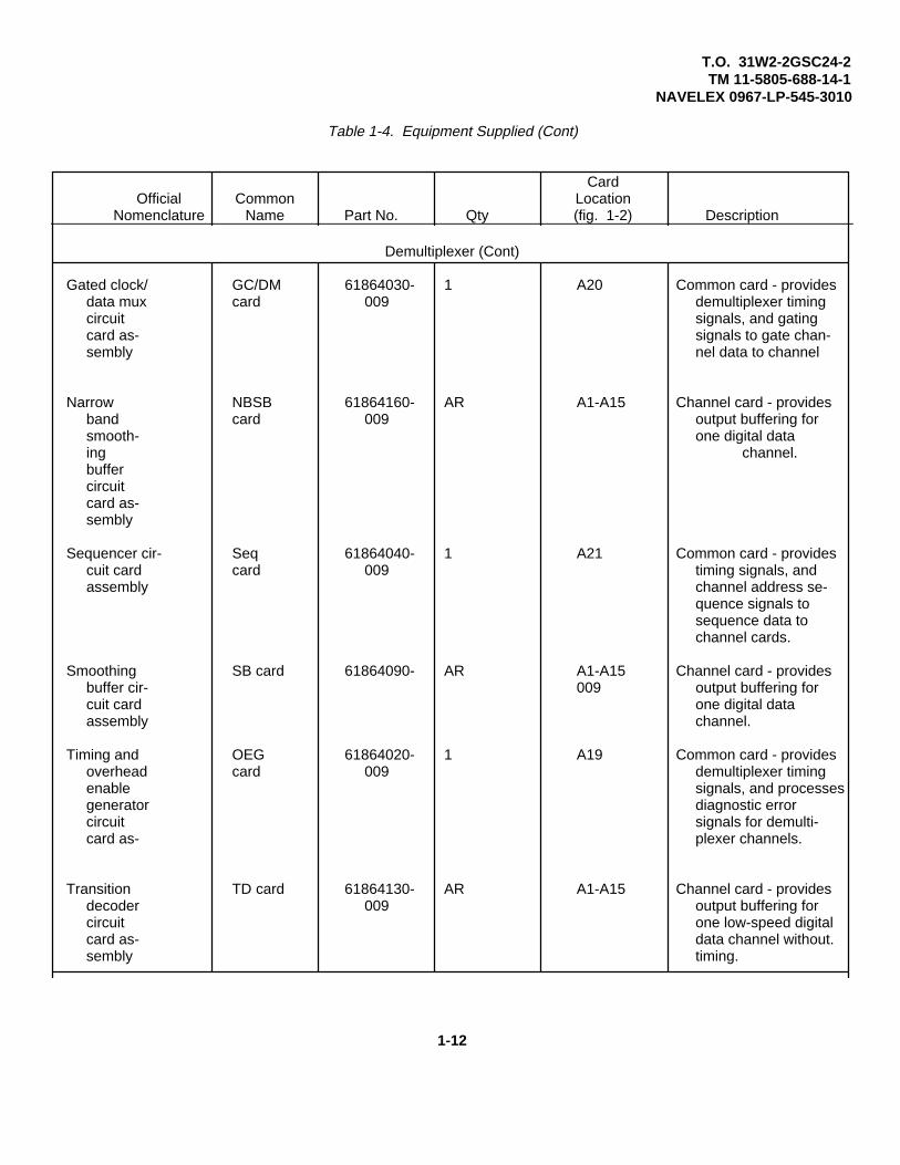
T.O. 31W2-2GSC24-2TM 11-5805-688-14-1
NAVELEX 0967-LP-545-3010
Table 1-4. Equipment Supplied (Cont)
CardOfficial Common Location
Nomenclature Name Part No. Qty (fig. 1-2) Description
Demultiplexer (Cont)
Gated clock/ GC/DM 61864030- 1 A20 Common card - providesdata mux card 009 demultiplexer timingcircuit signals, and gatingcard as- signals to gate chan-sembly nel data to channel
Narrow NBSB 61864160- AR A1-A15 Channel card - providesband card 009 output buffering forsmooth- one digital dataing channel.buffercircuitcard as-sembly
Sequencer cir- Seq 61864040- 1 A21 Common card - providescuit card card 009 timing signals, andassembly channel address se-
quence signals tosequence data tochannel cards.
Smoothing SB card 61864090- AR A1-A15 Channel card - providesbuffer cir- 009 output buffering forcuit card one digital dataassembly channel.
Timing and OEG 61864020- 1 A19 Common card - providesoverhead card 009 demultiplexer timingenable signals, and processesgenerator diagnostic errorcircuit signals for demulti-card as- plexer channels.
Transition TD card 61864130- AR A1-A15 Channel card - providesdecoder 009 output buffering forcircuit one low-speed digitalcard as- data channel without.sembly timing.
1-12

T.O. 31W2-2GSC24-2TM 11-5805-688-14-1
NAVELEX 0967-LP-545-3010
Table 1-4. Equipment Supplied (Cont)
CardOfficial Common Location
Nomenclature Name Part No. Qty (fig. 1-2) Description
Demultiplexer (Cont)
Voice de- VD card 61864140- AR Al-Al5 Channel card - providescoder cir- 009 digital- to -analog out-cuit card put interface for oneassembly voice channel.
Additional Equipment
Cable as- Power 61861700- 1 AC power input cable.sembly cable 009(power)
Connector 61867000- Variable Mating connectors for rearset 009 and panel Twinax recep-assembly -019 tacles. Quantity
determined by channelrequirements.
Table 1-5. Related Technical Publications
EquipmentPublication Number Publication Title Nomenclature
T.O. 31W2-2GSC24-3 Technical Manual - Circuit AN/GSC-24(V)(Air Force) Diagrams multiplexer set
T.M. 11-5805-688-14-2(Army)
NAVELEX 0967-LP-545-3020 (Navy)
T.O. 31W2-2GSC24-4 Technical Manual - Illustrated AN/GSC-24(V)(Air Force) Parts Breakdown multiplexer set
T.M. 11-5805-688-14-3(Army)
NAVELEX 0967-LP-545-3030 (Navy)
T.O. 31W2-2GSC24-6WC-1 Scheduled Periodic Work Cards AN/GSC-24(V)multiplexer set
1-13

T.O. 31W2-2GSC24-2TM 11-5805-688-14-1
NAVELEX 0967-LP-545-3010
Table 1-5. Related Technical Publications (Cont)
EquipmentPublication Number Publication Title Nomenclature
T.O. 31W-1-06-2 Work Unit Code Manual AN/GSC-24(V)multiplexer set
To be assigned Technical Manual - Harris Model To be assigned7003 Data Communications TestSet
To be assigned Technical Manual - Power Supply To be assignedTest Set
To be assigned Technical Manual for Subassembly To be assignedTest Set
Table 1-6. Special Tools List(Equivalent equipment is authorized.)
Part Mfr Code or(Tool) Name/ Figure and Use
Number Address Index No. Nomenclature (para)
SK62759367 09439 Wire-wrap repair toolset consisting of:
14XA2-B3C-(28) 24047 6-7 Wire wrapping tool 6-28
507100 24047 6-7 Wrapping sleeve 6-28
508748 24047 6-7 Wrapping kit 6-28
511203 24047 Unwrapping tool 6-28
515654 24047 6-7 Cut/strip accessory 6-28
SK63759367 04939 Connector repair tool 6-66set consisting of:
CCT-DL 71468 Hand crimp tool
CET-DL-2 71468 Extraction tool
CET 12-14 71468 Extraction tool
CET 6CB 71468 Extraction tool
MS18278-1 96906 Insertion/extractiontool
274-7304-00 71468 Contact Removal Tool
Change 2 1-14

T.O. 31W2-2GSC24-2TM 11-5805-688-14-1
NAVELEX 0967-LP-545-3010
Table 1-6. Special Tools List (Cont)(Equivalent equipment is authorized.)
Part Mfr Code or(Tool) Name/ Figure and Use
Number Address Index No. Nomenclature (Para)
M22520/2-01 Crimp tool
M22520/2-08 Crimp tool
WT-311 59730 Crimp tool
Chassis repair tool Note 1.set consisting of:
B22 98291 6-24 Insertion tool
CHM1 72962 6-20 Handle
CHM2 72962 6-20 Handle
CPFA10 72962 6-20 Punch
CPFA6 72962 6-20 Punch
CPFB6 72962 6-20 Dolly
CPFB8 72962 6-20 Dolly
HT-1 98291 6-24 Hand insertion tool
H7503-10 08524 6-17 Installation tool
KT7200 92631 6-22 Handle
KT7202-046 92631 6-22 Squeeze tool
KT7202-083 92631 6-22 Squeeze tool
29-47-101-10 94222 6-16 Installation tool
TK-105/G Electronic equipment Note 2.tool kit
NOTES: 1. Depot level use only.2. General Repair at intermediate and depot level.
Change 2 1-15

T.O. 31W2-2GSC24-2TM 11-5805-688-14-1
NAVELEX 0967-LP-545-3010
Table 1-7. Test Equipment List(Equivalent equipment is authorized.)
Table 1-6.Type Alternate Type Figure Use
Designation Designation No. Nomenclature (para)
GR Model Decade Resistance Box Note 31321-NHARRIS Model Digital communications 6-427003 test setHP Model 204D Signal generator Note 3HP Model 331A Distortion Analyzer Note 3HP Model 3310A Function generator Notes 3, 4HP Model 3400A Voltmeter Note 3HP Model 3490A Digital Multimeter Notes 3, 4HP Model 3550B Portable test set 6-41HP Model 3555B Transmission and noise Note 3
meterHP Model 4329A Insulation resistance Note 4HP Model 5245M Frequency counter 6-34, 35
Notes 3, 4HP Model 6205B Power supply Notes 3, 4HP Model 630A Multimeter Note 1Tektronix Oscilloscope main frame Note 1Model R7704A
Model P6063A Probe Notes 1, 2Model 7A26 Dual vertical amplifier Notes 1, 2Model 7B92 Time base Notes 1, 2Model 7D15 Universal counter Notes 1, 2
61868300-009 Power supply test set Note 561868000-009 Subassembly test set Note 6
NOTES:1. General troubleshooting at intermediate and depot level.2. Used with oscilloscope main frame.3. Used with subassembly test set for printed circuit card maintenance at depot level4. Used with power supply test set for power supply maintenance at depot level.5. Power supply maintenance at depot level.6. Printed circuit card maintenance at depot level.
Change 2 1-16

T.O. 31W2-2GSC24-2TM 11-5805-688-14-1
NAVELEX 0967-LP-545-3010
CHAPTER 2
INSTALLATION
SECTION I
INSTALLATION LOGISTICS2-1. GENERAL..
2-2. This section contains general instructions forunpacking and storing the multiplexer set prior toinstallation as prescribed in section II.
2-3. UNLOADING AND UNPACKING.
The multiplexer set weighs 140pounds. Use a mechanical liftingdevice whenever possible. Toprevent injury to personnel, it isrecommended that a minimum offour men be used when amultiplexer set is to be liftedmanually.
2-4. During the unpacking procedures, the multiplexerset should be positioned on a firm, level surface in anarea that is protected from the elements. No special orunique procedures are required for unpacking themultiplexer set.
NOTE
Use care when opening the shippingcontainer to prevent unnecessarydamage to the container so that it maybe stored and reused for repacking amultiplexer set for reshipment.
1. Open the shipping container and carefullyremove loose padding and fill material.
Use care when lifting multiplexerset from container to preventdamage to protruding controls,indicators, and receptacles on theunit.
2. Remove multiplexer set from shipping container.Remove moisture resistant barrier material frommultiplexer set.
3. Inspect exterior surfaces of multiplexer set forshipping damage, missing or damaged controls andindicators, and evidence of water damage.
4. Check received equipment against shippingdocuments and/or packing slip.
5. When equipment is incomplete or damaged, fillout and forward appropriate forms in accordance withprescribed directives.
2-5. STORAGE HOUSING REQUIREMENTS.
2-6. The multiplexer set should be housed to protect itfrom inclement weather. The unit should be storedwithin an ambient temperature range of -80° to +160°F (-62° to +71°C). The multiplexer set in a nonoperatingcondition can be stored at altitudes from sea level to50,000 feet (3.44 inches Hg). The multiplexer set can bestored on a flat surface capable of supporting 50 poundsper square foot. The accessories listed in paragraph 2-8should be inventoried
2-1

T.O. 31W2-2GSC24-2TM 11-5805-688-14-1
NAVELEX 0967-LP-545-3010
and stored with the multiplexer set or in a areadesignated for storage of small items.
2-7. RECEIVING DATA.
2-8. The multiplexer set is shipped with a set of plug-incards installed in the unit. The quantity and type of plug-in cards will be determined by system application of theequipment. The appropriate shipping literature willidentify the quantity and card types. Two separateaccessories are shipped with the multiplexer set: powercable assembly P/N 61861700-009 (ac power cable) andconnector kit assembly P/N 61867000009 or P/N61867000-019. The contents of each connector kitassembly are listed in the following chart.
2-9. INSTALLATION HOUSING REQUIREMENTS.
2-10. The multiplexer set is constructed so that it can bemounted in a standard
19-inch relay rack or equivalent. The ruggedized chassisalso allows the multiplexer set to be installed on a flat,open surface that is capable of supporting 50 pounds persquare foot. The installation data in table 2-1 should beconsidered when selection of an installation location forthe multiplexer set is under consideration.
Quantity
Item/Part No. -019 -009
Backshell M83723-15S-14 1 1
Plug MS3476E14-19S 1 1
Connector plug 37 65(Bendix P/N33449-1)
Table 2-1. Installation Data
Item Data
Chassis dimensions
Height 24.5 inches
Depth 19.0 inches
Width 17.0 inches
Chassis weight 140 pounds
Rack requirement Standard 19-inch relay rack that is firmly mounted to afloor to prevent tipping when multiplexer set ismounted on slides and extended out of rack.
2-2

T.O. 31W2-2GSC24-2TM 11-5805-688-14-1
NAVELEX 0967-LP-545-3010
Table 2-1. Installation Data (Cont)
Item DataRack clearances
Front Allow approximately 48 inches for installation or removalof multiplexer set from rack. Allow same area forservicing multiplexer set extended on slides forservicing.
Rear Allow approximately 24 inches for routing of cableassemblies connected to rear of multiplexer set,and for circulation of exhaust air from cooling airblower in upper rear of multiplexer set.
Operating position Normal (level) to 90° inclination
Operating temperature 0°to +125° F (-18° to +52°C) ambient temperature
Operating altitude Sea level to 10,000 feet (20.58 inches Hg)
Primary power 115 vac +10%, single phase, 47 to 410 Hz
Power dissipation 634 watts
Electrical connectorson rear panel
Signal (timing and data) Bendix 30340-5 or equivalent - mates with Bendix33449-1 or equivalent.
Signal (remote alarm) MS3470E14-19P - mates with MS3470E14-19S
Power MS3126F12-3P - mates with MS3126F12-3S
SECTION II
INSTALLATION PROCEDURES
2-11. GENERAL.
2-12. This section contains general instructions forinstalling the multiplexer set in a standard 19-inch relayrack. Since there are different equipment rackconfigurations in which the multiplexer set may beinstalled, it may be necessary to modify the installationprocedures for a particular installation.
As specified in the following procedures, a multiplexerset can be installed in a rack in one of two ways: the unitcan be mounted and supported in a rack by the two slideassemblies (figure 1-1) provided (paragraph 2-13); or theunit can be bolted directly in a rack, using the two rack-mounting flanges (figure 1-1) on the front of the chassis(paragraph 2-15).
2-3

T.O. 31W2-2GSC24-2TM 11-5805-688-14-1
NAVELEX 0967-LP-545-3010
2-13. INSTALLATION PROCEDURES.
NOTE
Before installing a multiplexerset in a rack, check theinstallation data in table 2-1 toensure the mounting andoperating conditions areadequate.
2-14. Perform the following procedures to install themultiplexer set in a rack, using the slide assemblies.
1. Determine the exact physical position inwhich the multiplexer set will be mounted in the rack.Then determine the positions in which the two slideassemblies on the chassis will be attached to the rackframe. Remove the outer section of each slide assemblyand use it as a template to mark the locations where theforward and aft pairs of mounting holes align with theinterior of the rack frame. If required, mark and drill rackframe as necessary to mount the slide assembly to therack frame.
When performing step 2, secureeach outer slide section to rackframe, using four screws. The useof less than eight screws (four oneach side) to secure the two outerslide sections may cause themultiplexer set to break loose andcause serious injury to personnel.
2. Connect each outer slide section to the rackframe, using a minimum of four 10-32 (minimum size)screws with flat washers, lockwashers, and nuts.
3. Note that sufficient clearance is provided forinsertion of remaining slide sections into the front of therack-mounted outer slide sections. If such clearance isnot provided or is marginal, the forward lip of the rackshould be suitably notched.
4. Fully extend (toward rear of chassis) the twoinner slide sections attached to each side of themultiplexer set chassis.
A multiplexer set weighs 140pounds. Use a mechanicallifting device whenever possible.To prevent injury to personnel, itis recommended that a minimumof four men be used when amultiplexer set is to be liftedmanually.
5. Lift multiplexer set and position extendedinner slide sections on unit so that they mate with outerslide sections installed in rack. Slowly positionmultiplexer set fully into rack until rack-mounting flangeson multiplexer set contact the front of the rack frame.
6. With multiplexer set in place in rack, installtwelve 10-32 (minimum size) screws, with washers, tosecure rack-mounting flanges on multiplexer set to rack.
7. On rear of multiplexer set, connect powercable assembly to POWER INPUT receptacle on unitand to a suitable ac power source outlet.
8. Connect signal cables between receptacleson rear of multiplexer set
2-4

T.O. 31W2-2GSC24-2TM 11-5805-688-14-1
NAVELEX 0967-LP-545-3011
as prescribed for the specific system configuration.
9. Remove front cover from multiplexer set(figure 1-1) and ensure that the plug-in card complementis correct for the designated system application.
10. Visually inspect plug-in cards and interior ofmultiplexer set for damage.
11. Perform the procedures prescribed insection III of chapter 3 to electrically configure themultiplexer set for the selected system application.
2-15. Perform the following procedures to mount amultiplexer set to a rack, using only the two rack-mounting flanges on the multiplexer set.
1. Determine the exact physical location inwhich the multiplexer set will be mounted in the rack.
NOTE
When the two slide assemblies on themultiplexer set interfere with theinstallation of the unit in a rack, theslide assemblies should be removedas prescribed in step 2. If the slideassemblies are already removed ordo not interfere with the installation,proceed to step 3.
2. Remove two slide assemblies from chassisby removing seven screws securing each slide assemblyto multi-
plexer set. Store removed slide assemblies for futureuse.
A multiplexer set weighs 140 pounds.Use a mechanical lifting device wheneverpossible. To prevent injury to personnel,it is recommended that a minimum offour men be used when a multiplexer setis to be lifted manually.
3. Lift multiplexer set into rack and secure rack-mounting flanges to rack frame, using twelve 10-32(minimum size) screws with washers.
4. On rear of multiplexer set, connect powercable assembly to POWER INPUT receptacle on unitand to a suitable ac power source outlet.
5. Connect signal cables between receptacleson rear of multiplexer set as prescribed for the specificsystem configuration.
6. Remove front cover (figure 1-1) and note thatthe plug-in card complement is correct for the designatedsystem application. Visually inspect plug-in cards andinterior of multiplexer set for damage.
7. Perform the procedures prescribed in sectionIII of chapter 3 to electrically configure the multiplexer setfor the selected system application.
Change 1 2-5/2-6

T.O. 31W2-2GSC24-2TM 11-5805-688-14-1
NAVELEX 0967-LP-545-3010
CHAPTER 3
PREPARATION FOR USE
SECTION I
GENERAL
3-1. INTRODUCTION.
3-2. This section and sections II and III containintroductory information and detailed instructions forpreparing the multiplexer set for operation. Instructionsfor preparing the multiplexer set for reshipment areprescribed in section IV.
3-3. This section contains general information about themultiplexer set and its application within various datacommunications systems. The purpose of this section isto assist the user in understanding equipmentconfiguration planning as prescribed in sections II and III.
3-4. Detailed instructions for configuration of an actualmultiplexer set are contained in section III. Theprocedures are predicated upon the availability of a setof completed configuration worksheets. Section IIdescribes, by example, procedures for preparing theworksheets and also discusses supplemental factors thatshould be considered in planning a multiplexer setsystem application. Normally, the user is provided withworksheets that describe how a multiplexer set is to beconfigured for a specific application. In such cases, theuser may regard the instructions in section II assupplementary information.
3-5. TYPICAL SYSTEM APPLICATIONS.
3-6. The multiplexer set is a flexible equipment capableof simultaneously performing multiplexing anddemultiplexing functions. Except for operating powerand certain display and alarm
features, the functions are independent of each other.Because of their functional independence, a multiplexerand demultiplexer within a given equipment may each beconfigured to simultaneously process channel data ofdifferent and unrelated forms.
3-7. Figure 3-1 depicts the multiplexer set in typicalduplex system applications. As shown in configuration Aof figure 3-1, input channels of the forms a, b, and c areapplied to the multiplexer (MUX) function of multiplexerset No. 1. These inputs are combined (multiplexed) intoa single output data stream and are routed via atransmission link to a far-end demultiplexer (DEMUX)that is a part of multiplexer set No. 2. Channels a, b,and c are outputs of the far-end demultiplexer, and aresubsequently routed to the assigned users. In return, thefar-end multiplexer accepts channel inputs of the formsa, b, and c, and routes them via the transmission link tothe demultiplexer portion of multiplexer set No. 1. Thus,in this example, channel data of the same forms (a, b,and c) are transmitted in both directions.
3-8. Configuration B of figure 3-1 depicts anunsymmetrical duplex system application in whichchannel data transmitted in one direction are in adifferent form than the data transmitted in the otherdirection. This configuration is made possible by theindependence of multiplexer and demultiplexer functionswithin a given multiplexer set.
3-1

T.O. 31W2-2GSC24-2TM 11-5805-688-14-1
NAVELEX 0967-LP-545-3010
Figure 3-1. Typical Duplex Configurations
3-2

T.O. 31W2-2GSC24-2TM 11-5805-688-14-1
NAVELEX 0967-LP-545-3010
3-9. Figure 3-2 depicts the multiplexer set in typicalsimplex system configurations. In simplex systemapplications, the independence of multiplexer anddemultiplexer functions enables one function, or portionsthereof, to operate while the other function remainsunused. As shown in configuration A of figure 3-2, themultiplexer portion of multiplexer set No. 1 combinesinputs a, b, and c for transmission to a farenddemultiplexer that is a part of multiplexer set No. 2. Insuch an application, the near-end demultiplexer and far-end multiplexer functions are not used.
3-10. Configuration B of figure 3-2 depicts another typeof simplex application, which is sometimes referred to asa broadcast arrangement. In this application, data froma near-end multiplexer are transmitted to several farenddemultiplexers. Each demultiplexer is configured tooutput one (or more) of the channels applied to thetransmitting multiplexer. In such an arrangement, thenear-end demultiplexer, the far-end multiplexers, andportions of the farend demultiplexers are not used.
3-11. CHANNEL AND PORT RELATIONSHIPS.
3-12. Data applied to the multiplexer’s channel inputsare converted, when necessary, into a prescribed digitalform and are held in buffer storage until they aresynchronously inserted into the multiplexer’s serial outputdata stream. Since data from multiple channels mustenter this stream, they are inserted at a predeterminedtime in an established channel sampling sequence. Theinterval of time during which data from a given channelare allowed to enter the multiplexer’s output stream istermed a port. Thus, in a given multiplexer configuration,a port is permanently assigned to a particular channeland will convey that channel’s data into the multiplexer’soutput when the port occurs.
3-13. When a port assigned to a given channel occurs,a single bit of the channel data passes to themultiplexer’s output. Therefore, the rate at which theporting occurs must equal the channel’s input data rate(Rc). However, since the multiplexer set must be
capable of simultaneously accepting channel inputs ofdifferent rates, multiple ports may be assigned to a singlechannel. The number of ports thus assigned to a givenchannel may vary up to a maximum of 25, and is termedK. The assignment of more than one port to a givenchannel is termed port strapping. The first port assignedto a channel is known as the active port, and subsequentports assigned to that channel are known as strappedports. The product of the rate that each port is sampled,known as port rate (Rp), and the total number of ports
(K) assigned to a channel must be equal to or greaterthan the channel’s input data rate (Rc), or KRp > Rc. In a
given multiplexer configuration, the total number of portsassigned to the multiplexer’s channels is known as N,and must be an integer between 15 and 31.
3-14. Regardless of configuration, a single port withinthe multiplexer is automatically reserved for conveyingoverhead data generated within the multiplexer into themultiplexer’s output data stream. Thus, in any givenmultiplexer configuration, the total quantity of ports usedfor processing channel and overhead data is N + 1, andis between 16 and 32. The multiplexer’s output datarate, termed Ro, is simply the product of port rate (Rp)
and the total quantity (N + 1) of ports used, or Ro = Rp(N + 1).
3-15. The port assignments in a receiving demultiplexermust exactly match those used in the transmittingmultiplexer. This enables the demultiplexer todisassemble its serial input data stream into individualchannel outputs matching the multiplexer’s inputs. Inapplications where several
Change 2 3-3

T.O. 31W2-2GSC24-2TM 11-5805-688-14-1
NAVELEX 0967-LP-545-3010
Figure 3-2. Typical Simplex Configuration
3-4

T.O. 31W2-2GSC24-2TM 11-5805-688-14-1
NAVELEX 0967-LP-545-3010
demultiplexers are receiving inputs from a singlemultiplexer (paragraph 3-9), port assignments withineach demultiplexer must match those of the transmittingmultiplexer.
3-16. In summary, a port is an interval of time duringwhich a bit of data is inserted into the multiplexer’s serialoutput stream. For a given configuration, one or moreports may be assigned to a particular channel; the totalfor the channel is termed K. The product of K and therate at which porting occurs (Ro) must equal or exceed
the channel input rate (Ro). The total quantity of ports
assigned to channels in a given multiplexer configurationis termed N, and when the overhead port is considered,the total number of ports in use is N + 1. The value for N+ 1 varies between 16 and 32. Multiplexer output rate(Ro) is equal to Ro (N + 1). Regardless of system
application, port-to-channel assignments in a receivingdemultiplexer must exactly match those of thetransmitting multiplexer.
3-17. CHANNEL RATES AND FORMS.
3-18.The multiplexer set will accept and properly processcharnel inputs of varying forms and rates. Input formsinclude the following: digital data with associated timing;digital data
without associated timing; and voice data. The rates atwhich data inputs may occur depend upon the input formand the mode in which they are processed by themultiplexer set. Specific form and rate limitations arediscussed in paragraphs 3-19 through 3-24.
3-19. DIGITAL DATA WITH ASSOCIATED TIMING.
3-20. One of the channel input/output data formsaccepted and processed by the multiplexer set is digitaldata with associated timing. This data form is commonlyreferred to as Type I, and is illustrated in figure 3-3. Notethat one complete cycle of the input/output timing signaloccurs for each bit time (T) of the data signal in figure 3-3. The multiplexer set accepts and processes Type Ichannel data at any rate between 50 bps and 3.0 Mbps,provided the rate satisfies the expression:
R0.96 > K(1 - c)
KRp
where
Rc = channel data rate
Rp = port rate
K = number of ports assigned tothe channel
Figure 3-3. Typical Type I Channel Input/Output Data and Timing Waveforms
3-5

T.O. 31W2-2GSC24-2TM 11-5805-688-14-1
NAVELEX 0967-LP-545-3010
Normally, Rc is nominally equal to KRp. In cases where
Rc is not equal to KRp, the channel rate is adjusted
within the multiplexer set and processed at a rate of theform Rc = KRp. The rate adjustment process is termed
coarse rate conversion, and is performed completelywithin the multiplexer set. Therefore, although coarserate conversion may be used, the demultiplexer’schannel output rate is the same as the multiplexer’schannel input rate.
3-21. Type-I channel input/output rates may vary fromtheir assigned nominal value by plus or minus 250 partsper million (+250 ppm;. The multiplexer setautomatically compensates for such rate deviations,using a process of internal bit insertion and deletiontermed stuffing. The stuffing capability enables themultiplexer set to process channel input/outputs notsynchronous with the set or with each other. Forexample, a channel input rate of 1.0 Mbps that variesbetween 1.000250 and 0.999750 Mbps is properlyprocessed in the multiplexer set. Deviations appearingin a multiplexer input channel rate are automaticallyreinserted in the corresponding demultiplexer outputchannel rate. The multiplexer is therefore considered tobe transparent to applied rate variations withinprescribed limits.
3-22. DIGITAL DATA WITHOUT ASSOCIATEDTIMING.
3-23. A second form of input/output channel dataaccepted and processed by the multiplexer set is digitaldata without timing. This data form is commonly referredto as Type II data. When provided with Type II channeldata inputs, the multiplexer accepts the incoming dataand processes the data by means of timing signalsgenerated within the multiplexer. Data inputs of the
Type II form are processed within the multiplexer set bythe use of one of two techniques: timing recovery ortransition encoding/decoding. Type II data to beprocessed by the timing recovery technique must be atrates fitting the expression:
Rc = 75 x 2n bps
where
Rc = channel data rate
n = an integer from 0 to 7.
Rates fitting this expression are as follows:
n Rc(bps)
0 75
1 150
2 300
3 600
4 1200
5 2400
6 4800
7 9600
It is also required that Type II channel data processed bythe timing recovery technique reflect a sense transition(1 to 0, or 0 to 1) at least once each 100 data bit times.This enables the multiplexer to internally generate anappropriately synchronized timing signal for subsequentprocessing of the applied data. Type II data rates mayvary from their assigned nominal values in the samemanner as that described for Type I data rates(paragraph 3-21).
3-6

T.O. 31W2-2GSC24-2TM 11-5805-688-14-1
NAVELEX 0967-LP-545-3010
3-24. Type II data processed by the transitionencoding/decoding technique may occur at rates withinsix ranges as follows:
0 - 75 bps
0 - 100 bps
0 - 150 bps
0 - 200 bps
0 - 300 bps
0 - 400 bps
Upon entering the multiplexer set, data are processed byusing a 3-bit transition encoding/decoding process. Thisprocess entails use of a KRp that is three times the
upper limit of the data rate range selected. For example,a 75-bps channel rate input being processed with the 0to75-bps data rate range would require a KRp of 3 x 75 or
225 bps. It is not necessary that a given input data ratebe processed with only the lowest rate range in which itfalls. A lower input rate may be processed with any raterange whose upper limit is higher than the applied inputrate. Thus, for example, a channel input data rate of 100bps can be processed with the 0 to 150-bps rate range.It is also important to note that any input rate variationthat causes the input rate to exceed the upper limit of theselected rate range may cause data errors to be
generated by the multiplexer set. Therefore, if thenominal input data rate is at the upper limit of the raterange selected, and positive variations in the input rateare expected, it is best to select the next higher raterange. Type II channel data processed by themultiplexer using the transition encoding/decodingtechnique are supplied to the correspondingdemultiplexer channel output without associated timing.
3-25. VOICE DATA.
3-26. The multiplexer set will accept and process voicedata at frequencies within the range of 300 to 3400 Hz.Channel input/output impedance is 600 ohms(balanced).Full modulation occurs at a multiplexer input level of -16dBm. The corresponding demultiplexer output level is +7dBm. Processing of voice channel input data requiresuse of a KRp of 19.2 kbps or greater. A KRp of 38.4
kbps is preferred for voice processing.
3-27. CHANNEL CARD OPTIONS.
3-28. The channel input/output data forms discussed inparagraphs 3-19 through 3-26 are processed by meansof a variety of optional multiplexer and demultiplexerchannel cards. In appropriate combinations, the cardsare plugged into multiplexer and demultiplexer card slots1 through 15. Table 3-1 lists the optional channel cardsused within the multiplexer set, and identifies the channeldata form with which each card is associated.
Change 2 3-7

T.O. 31W2-2GSC24-2TM 11-5805-688-14-1
NAVELEX 0967-LP-545-3010
Table 3-1. Multiplexer Set Channel Card Options
Channel Data Form Multiplexer Channel Card Demultiplexer Channel Card
Type I, digital Rate comparison buffer (RCB), Smoothing buffer (SB),data with asso- P/N 61864010 P/N 61864090ciated timing
Type I, digital Rate comparison buffer (RCB), Narrow band smoothingdata with asso- P/N 61864010 buffer (NBSB), P/N 61864160ciated timing(special smooth-ing applications(paragraph 3-58)
Type II, digital Transition encoder/timing Smoothing buffer (SB),data without recovery (TE/TR), P/N 61864090associated tim- P/N 61864060ing (timing re-covery process-ing technique)
Type II, digital Transition encoder/timing Transition decoder (TD),data without recovery (TE/TR), P/N 61864130associated tim- P/N 61864060ing (transitionencoding/decoding tech-nique)
Voice data Voice encoder (VE), Voice decoder (VD), P/N 61864140P/N 61864070
SECTION II
PREPARATION OF CONFIGURATION WORKSHEETS
3-29. GENERAL.
3-30. In configuring the multiplexer set as prescribed insection III, the user must have certain information tosatisfy a particular set of system applicationrequirements. The information includes a definition ofchannel input/ output data rates, port assignmentinstructions, multiplexer output rate, etc. The requiredconfiguration information is recorded on a four-page set
of configuration worksheets; the worksheets perform thebasic functions listed in table 3-2.
3-31. Figure 3-4 depicts the system applicationrequirement that is used as an example in the followingdiscussions on the preparation of the configurationworksheets. More specifically, the discussions center onthe preparation of the worksheets to enable theconfiguration of multiplexer set
3-8

T.O. 31W2-2GSC24-2TM 11-5805-688-14-1
NAVELEX 0967-LP-545-3010
Table 3-2. Configuration Worksheet Data
Sheet FigureNo. No. Function
1 3-5 Provides information necessary to configure channel electronics portion of multiplexerfunction. Includes information defining channel input rates and forms, andinstructions as to type f channel card to be used in processing each channel input.
2 3-6 Provides information necessary to configure common electronics portion of multiplexerfunction. Includes information defining output rate (Ro) and form, port assignments,and timing source.
3 3-7 Provides information necessary to configure channel electronics portion ofdemultiplexer function. Includes information defining channel output rates andforms, and instructions as to type of channel card to be used in processing eachchannel output.
4 3-8 Provides information necessary to configure common electronics portion ofdemultiplexer function. Includes information defining serial data high-speed inputrate (Ro), port assignments, and timing source.
No. 1 in the selected system. In the duplex arrangementshown in figure 3-4, both the multiplexer anddemultiplexer are used, but with different sets of channeldata rates and forms. A mix of voice, Type I, and Type II(paragraphs 3-20 through 3-26) channel inputs is appliedto the multiplexer set. The inputs are multiplexed into asingle 48.0-kbps output data stream. The demultiplexeraccepts a serial 1.536-Mbps input data stream anddemultiplexes it into five Type I channel data outputs.
3-32. MULTIPLEXER CHANNEL ELECTRONICS.
3-33. Sheet 1 of the configuration worksheets (figure 3-5) is prepared to enable setup of the multiplexer channelcards. As shown in the configuration example in figure3-4, five channels are used to accept a mixture of voiceand Type I and Type II data inputs.
3-34. On sheet 1 of the configuration worksheets, eachchannel’s input rate is entered in the applicable INPUTRATE (BPS) Rc block. Since the channel 2 input is
voice, the word VOICE is entered instead of a data rate.Next, the type of channel card to be used for theprocessing of each input channel is listed in theapplicable CARD TYPE TE/TR, VE, or RCB block.Thus, for channel 2, an X is entered in the VE (voiceencoder) block. Channels 1 and 3 process Type II datainputs that do not have an associated timing input. Suchinputs must be processed with a transitionencoder/timing recovery (TE/TR) card (paragraph 3-28)operating in either the transition encoder (TE) or timingrecovery (TR) mode. A maximum input rate of 400 bpscan be processed in the TE mode, and KRp must be
three times the selected input rate range (paragraph 3-24). In the TR mode, the
Change 2 3-9

T.O. 31W2-2GSC24-2TM 11-5805-688-14-1
NAVELEX 0967-LP-545-3010
Figure 3-4. Example of Multiplexer Set Configuration
3-10
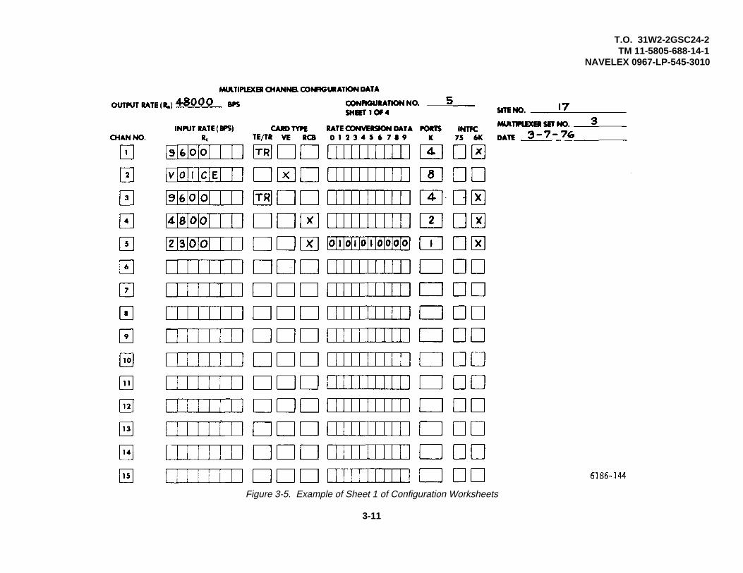
T.O. 31W2-2GSC24-2TM 11-5805-688-14-1
NAVELEX 0967-LP-545-3010
Figure 3-5. Example of Sheet 1 of Configuration Worksheets
3-11

T.O. 31W2-2GSC24-2TM 11-5805-688-14-1
NAVELEX 0967-LP-545-3010maximum input rate may be 9600 bps (paragraph 3-23).Since the 9600-bps input rate applied to channels 1 and3 exceeds the maximum TE input rate and KRp is not 3x Rc, the TR processing mode is selected. Therefore, theletters TR (timing recovery) are entered in the CARDTYPE TE/TR block for these two channels. Channels 4and 5 process Type I data inputs, and therefore an X isentered in the CARD TYPE RCB block for each channel(paragraph 3-27). In the INTFC block for each channel,an X is entered in either the 75 or 6K (ohms) block, asappropriate, to match the channel source impedance forthe given installation under consideration. For example,in figure 3-5, the INTFC block for channel 2 is notmarked since the voice input impedance of 600 ohms(balanced) is fixed by channel card design. In theexample shown, the source impedance for all digitalchannel inputs is assumed to be 6K ohms. Theworksheet is completed upon entry of the multiplexeroutput rate (Ro) value of 48000 in the OUTPUT RATE(Ro) BPS block, and entry of the number of the ports (K)assigned to each channel into the PORTS K blocks.
3-35. It should be noted that the input rate (Rc) of 2300bps for channel 5 is less than that channel’s KRp of 2400bps. In such a situation, coarse rate conversion to KRpmust be performed (paragraph 3-19). To enableconversion, a 10-digit binary number is computed andentered on the worksheet. Normally, the computation isperformed as part of the actual multiplexer setupprocess. However, as a convenience to the personsetting up the multiplexer, it may be performed at thetime the worksheet is prepared. Computationprocedures are prescribed in paragraph 3-69, steps 7and 8.The maximum number of fill bits that may beinserted is 868 bits. A computed fill bit quantity greaterthan 868 is indicative of an attempted coarse rateconversion that is beyond the capabilities of themultiplexer set. Based
on these procedures, the quantity of fill bits required is:R
Fill bits = (899) (K) (1 - c)KR
p= (899) (1) (1 - 0.9583333)
= 37.46
= 37
Since this number is < 868, the conversion may beperformed. As shown in table 3-3, the 10-digit binarynumber that must be used to cause the injection of 37 fillbits is 0101010000 (LSB left) This number is thenentered in the RATE CONVERSION DATA block of theworksheet (figure 3-5).
3-36. MULTIPLEXER COMMON ELECTRONICS.
3-37. Sheet 2 of the configuration worksheets (figure 3-6) is prepared to enable setup of the cards in themultiplexer common electronics section. The individualpreparing the worksheet uses portions of the informationin figure 3-4, combined with a knowledge of the electricalinterface cabling and termination arrangements that existwithin the facility in which the multiplexer set is installed.
3-38. In figure 3-4, the multiplexer output rate (Ro) isshown as 48.0 kbps; the value 48000 is thereforeentered in the OUTPUT RATE (Ro) BPS block of theworksheet. Reference timing is supplied in the form ofan external 3.072-MHz station clock. Therefore, an X isentered in the SOURCE EXT block, and the value3072000 is entered in the EXT FREQ HZ block. Allmultiplexer set interface circuits are designed to providean input/output impedance of 6K ohms or 75 ohms. Theimpedance that matches the station clock source shouldbe selected. For this example, it is assumed that 75ohms is the proper match; therefore, an X is entered inthe INPUT INTFC 75 block.
3-12

T.O. 31W2-2GSC24-2TM 11-5805-688-14-1
NAVELEX 0967-LP-545-3010
Table 3-3. Coarse Rate Conversion Strapping Data
Fill Card Strapping Fill Card Strapping Fill Card StrappingBits 0123456789 Bits 0123456789 Bits 0123456789
0 0000000000 46 0010110000 92 11010110001 1000000000 47 1010110000 93 00110110002 0100000000 48 0110110000 94 10110110003 1100000000 49 1110110000 95 01110110004 0010000000 50 1001110000 96 11110110005 1010000000 51 0101110000 97 10001110006 0110000000 52 1101110000 98 01001110007 1110000000 53 1011110000 99 11001110008 1001000600 54 0111110000 100 00101110009 0101000000 55 1111110000 101 1010111000
10 1010000000 56 1000001000 102 011011100011 0110000000 57 0100001000 103 111011100012 0110000000 58 1100001000 104 100111100013 1110000000 59 0010001000 105 010111100014 1110000000 60 1010001000 106 110111100015 0001000000 61 0110001000 107 101111100016 1001000000 62 1110001000 108 011111100017 1001000000 63 1001001000 109 111111100018 0101000000 64 0101001000 110 100000010019 0101000000 65 1101001000 111 010000010020 0110100000 66 0011001000 112 110000010021 1110100000 67 1011001000 113 001000010022 1001100000 68 0111001000 114 101000010023 0101100000 69 1111001000 115 011000010024 1101100000 70 1000101000 116 111000010025 0011100000 71 0100101000 117 100100010026 1011100000 72 1100101000 118 010100010027 0111100000 73 0010101000 119 110100010028 1111100000 74 1010101000 120 001100010029 1000010000 75 0110101000 121 101100010030 0100010000 76 1110101000 122 011100010031 1100010000 77 1001101000 123 111100010032 0010010000 78 0101101000 124 100010010033 1010010000 79 1101101000 125 010010010034 0110010000 80 1011101000 126 110010010035 1110010000 81 0111101000 127 001010010036 1001010000 82 1111101000 128 101010010037 0101010000 83 1000011000 129 011010010038 1101010000 84 0100011000 130 111010010039 0011010000 85 1100011000 131 100110010040 1011010000 86 0010011000 132 010110010041 0111010000 87 1010011000 133 110110010042 1111010000 88 0110011000 134 101110010043 1000110000 89 1110011000 135 011110010044 0100110000 90 1001011000 136 111110010045 1100110000 91 0101011000 137 1000010100
3-13

T.O. 31W2-2GSC24-2TM 11-5805-688-14-1
NAVELEX 0967-LP-545-3010
Table 3-3. Coarse Rate Conversion Strapping Data (Cont)
Fill Card Strapping Fill Card Strapping Fill Card StrappingBits 0123456789 Bits 0123456789 Bits 0123456789
138 0100010100 184 1110101100 230 0111000010139 1100010100 185 1001101100 231 1111000010140 0010010100 186 0101101100 232 1000100010141 1010010100 187 1101101100 233 0100100010142 0110010100 188 1011101100 234 1100100010143 1110010100 189 0111101100 235 0010100010144 1001010100 190 1111101100 236 1010100010145 0101010100 191 1000011100 237 0110100010146 1101010100 192 0100011100 238 1110100010147 0011010100 193 1100011100 239 1001100010148 1011010100 194 0010011100 240 0101100010149 0111010100 195 1010011100 241 1101100010150 1111010100 196 0110011100 242 0011100010151 1000110100 197 1110011100 243 1011100010152 0100110100 198 1001011100 244 0111100010153 1100110100 199 0101011100 245 1111100010154 0010110100 200 1101011100 246 1000010010155 1010110100 201 0011011100 247 0100010010156 0110110100 202 1011011100 248 1100010010157 1110110100 203 0111011100 249 0010010010158 1001110100 204 1111011100 250 1010010010159 0101110100 205 1000111100 251 0110010010160 1101110100 206 0100111100 252 1110010010161 1011110100 207 1100111100 253 1001010010162 0111110100 208 0010111100 254 0101010010163 1111110100 209 1010111100 255 1101010010164 1000001100 210 0110111100 256 0011010010165 0100001100 211 1110111100 257 1011010010166 1100001100 212 1001111100 258 0111010010167 0010001100 213 0101111100 259 1111010010168 1010001100 214 1101111100 260 1000110010169 0110001100 215 1011111100 261 0100110010170 1110001100 216 0111111100 262 1100110010171 1001001100 217 1111111100 263 0010110010172 0101001100 218 1000000010 264 1010110010173 1101001100 219 0100000010 265 0110110010174 0011001100 220 1100000010 266 1110110010175 1011001100 221 0010000010 267 1001110010176 0111001100 222 1010000010 268 0101110010177 1111001100 223 0110000010 269 1101110010178 1000101100 224 1110000010 270 1011110010179 0100101100 225 1001000010 271 0111110010180 1100101100 226 0101000010 272 1111110010181 0010101100 227 1101000010 273 1000001010182 1010101100 228 0011000010 274 0100001010183 0110101100 229 1011000010 275 1100001010
3-14

T.O. 31W2-2GSC24-2TM 11-5805-688-14-1
NAVELEX 0967-LP-545-3010
Table 3-3. Coarse Rate Conversion Strapping Data (Cont)
Fill Card Strapping Fill Card Strapping Fill Card StrappingBits 0123456789 Bits 0123456789 Bits 0123456789
276 0010001010 322 0101111010 368 1000110110277 1010001010 323 1101111010 369 0100110110278 0110001010 324 1011111010 370 1100110110279 1110001010 325 0111111010 371 0010110110280 1001001010 326 1111111010 372 1010110110281 0101001010 327 1000000110 373 0110110110282 1101001010 328 0100000110 374 1110110110283 0011001010 329 1100000110 375 1001110110284 1011001010 330 0010000110 376 0101110110285 0111001010 331 1010000110 377 1101110110286 1111001010 332 0110000110 378 1011110110287 1000101010 333 1110000110 379 0111110110288 0100101010 334 1001000110 380 1111110110289 1100101010 335 0101000110 381 1000001110290 0010101010 336 1101000110 382 0100001110291 1010101010 337 0011000110 383 1100001110292 0110101010 338 1011000110 384 0010001110293 1110101010 339 0111000110 385 1010001110294 1001101010 340 1111000110 386 0110001110295 0101101010 341 1000100110 387 1110001110296 1101101010 342 0100100110 388 1001001110297 1011101010 343 1100100110 389 0101001110298 0111101010 344 0010100110 390 1101001110299 1111101010 345 1010100110 391 0011001110300 1000011010 346 0110100110 392 1011001110301 0100011010 347 1110100110 393 0111001110302 1100011010 348 1001100110 394 1111001110303 0010011010 349 0101100110 395 1000101110304 1010011010 350 1101100110 396 0100101110305 0110011010 351 1011100110 397 1100101110306 1110011010 352 0111100110 398 0010101110307 1001011010 353 1111100110 399 1010101110308 0101011010 354 1000010110 400 0110101110309 1101011010 355 0100010110 401 1110101110310 0011011010 356 1100010110 402 1001101110311 1011011010 357 0010010110 403 0101101110312 0111011010 358 1010010110 404 1101101110313 1111011010 359 0110010110 405 1011101110314 1000111010 360 1110010110 406 0111101110315 0100111010 361 1001010110 407 1111101110316 1100111010 362 0101010110 408 1000011110317 0010111010 363 1101010110 409 0100011110318 1010111010 364 0011010110 410 1100011110319 0110111010 365 1011010110 411 0010011110320 1110111010 366 0111010110 412 1010011110321 1001111010 367 1111010110 413 0110011110
3-15

T.O. 31W2-2GSC24-2TM 11-5805-688-14-1
NAVELEX 0967-LP-545-3010
Table 3-3. Coarse Rate Conversion Strapping Data (Cont)
Fill Card Strapping Fill Card Strapping Fill Card StrappingBits 0123456789 Bits 0123456789 Bits 0123456789
414 1110011110 460 1011100001 506 1100101001415 1001011110 461 0111100001 507 0010101001416 0101011110 462 1111100001 508 1010101001417 1101011110 463 1000010001 509 0110101001418 0011011110 464 0100010001 510 1110101001419 1011011110 465 1100010001 511 1001101001420 0111011110 466 0010010001 512 0101101001421 1111011110 467 1010010001 513 1101101001422 1000111110 468 0110010001 514 1011101001423 0100111110 469 1110010001 515 0111101001424 1100111110 470 1001010001 516 1111101001425 0010111110 471 0101010001 517 1000011001426 1010111110 472 1101010001 518 0100011001427 0110111110 473 0011010001 519 1100011001428 1110111110 474 1011010001 520 0010011001429 1001111110 475 0111010001 521 1010011001430 0101111110 476 1111010001 522 0110011001431 1101111110 477 1000110001 523 1110011001432 1011111110 478 0100110001 524 1001011001433 0111111110 479 1100110001 525 0101011001434 1111111110 480 0010110001 526 1101011001435 1000000001 481 1010110001 527 0011011001436 0100000001 482 0110110001 528 1011011001437 1100000001 483 1110110001 529 0111011001438 0010000001 484 1001110001 530 1111011001439 1010000001 485 0101110001 531 1000111001440 0110000001 486 1101110001 532 0100111001441 1110000001 487 1011110001 533 1100111001442 1001000001 488 0111110001 534 0010111001443 0101000001 489 1111110001 535 1010111001444 1101000001 490 1000001001 536 0110111001445 0011000001 491 0100001001 537 1110111001446 1011000001 492 1100001001 538 1001111001447 0111000001 493 0010001001 539 0101111001448 1111000001 494 1010001001 540 1101111001449 1000100001 495 0110001001 541 1011111001450 0100100001 496 1110001001 542 0111111001451 1100100001 497 1001001001 543 1111111001452 0010100001 498 0101001001 544 1000000101453 1010100001 499 1101001001 545 0100000101454 0110100001 500 0011001001 546 1100000101455 1110100001 501 1011001001 547 0010000101456 1001100001 502 0111001001 548 1010000101457 0101100001 503 1111001001 549 0110000101458 1101100001 504 1000101001 550 1110000101459 0011100001 505 0100101001 551 1001000101
3-16

T.O. 31W2-2GSC24-2TM 11-5805-688-14-1
NAVELEX 0967-LP-545-3010
Table 3-3. Coarse Rate Conversion Strapping Data (Cont)
Fill Card Strapping Fill Card Strapping Fill Card StrappingBits 0123456789 Bits 0123456789 Bits 0123456789
552 0101000101 598 1000001101 644 0110111101553 1101000101 599 0100001101 645 1110111101554 0011000101 600 1100001101 646 1001111101555 1011000101 601 0010001101 647 0101111101556 0111000101 602 1010001101 648 1101111101557 1111000101 603 0110001101 649 1011111101558 1000100101 604 1110001101 650 0111111101559 0100100101 605 1001001101 651 1111111101560 1100100101 606 0101001101 652 1000000011561 0010100101 607 1101001101 653 0100000011562 1010100101 608 0011001101 654 1100000011563 0110100101 609 1011001101 655 0010000011564 1110100101 610 0111001101 656 1010000011565 1001100101 611 1000101101 657 0110000011566 0101100101 612 1000101101 658 1110000011567 1101100101 613 0100101101 659 1001000011568 1011100101 614 1100101101 660 0101000011569 0111100101 615 0010101101 661 1101000011570 1111100101 616 1010101101 662 0011000011571 1000010101 617 0110101101 663 1011000011572 0100010101 618 1110101101 664 0111000011573 1100010101 619 1001101101 665 1111000011574 0010010101 620 0101101101 666 1000100011575 1010010101 621 1101101101 667 0100100011576 0110010101 622 1011101101 668 1100100011577 1110010101 623 0111101101 669 0010100011578 1001010101 624 1111101101 670 1010100011579 0101010101 625 1000011101 671 0110100011580 1101010101 626 0100011101 672 1110100011581 0011010101 627 1100011101 673 1001100011582 1011010101 628 0010011101 674 0101100011583 0111010101 629 1010011101 675 1101100011584 1111010101 630 0110011101 676 0011100011585 1000110101 631 1110011101 677 1011100011586 0100110101 632 1001011101 678 0111100011587 1100110101 633 0101011101 679 1111100011588 0010110101 634 1101011101 680 1000010011589 1010110101 635 0011011101 681 0100010011590 0110110101 636 1011011101 682 1100010011591 1110110101 637 0111011101 683 0010010011592 1001110101 638 1111011101 684 1010010011593 0101110101 639 1000111101 685 0110010011594 1101110101 640 0100111101 686 1110010011595 1011110101 641 1100111101 687 1001010011596 0111110101 642 0010111101 688 0101010011597 1111110101 643 1010111101 689 1101010011
Change 2 3-17

T.O. 31W2-2GSC24-2TM 11-5805-688-14-1
NAVELEX 0967-LP-545-3010
Table 3-3. Coarse Rate Conversion Strapping Data (Cont)
Fill Card Strapping Fill Card Strapping Fill Card StrappingBits 0123456789 Bits 0123456789 Bits 0123456789
690 0011010011 736 1100011011 782 1001100111691 1011010011 737 0010011011 783 0101100111692 0111010011 738 1010011011 784 1101100111693 1111010011 739 0110011011 785 1011100111694 1000110011 740 1110011011 786 0111100111695 0100110011 741 1001011011 787 1111100111696 1100110011 742 0101011011 788 1000010111697 0010110011 743 1101011011 789 0100010111698 1010110011 744 0011011011 790 1100010111699 0110110011 745 1011011011 791 0010010111700 1110110011 746 0111011011 792 1010010111701 1001110011 747 1111011011 793 0110010111702 0101110011 748 1000111011 794 1110010111703 1101110011 749 0100111011 795 1001010111704 1011110011 750 1100111011 796 0101010111705 0111110011 751 0010111011 797 1101010111706 1111110011 752 1010111011 798 0011010111707 1000001011 753 0110111011 799 1011010111708 0100001011 754 1110111011 800 0111010111709 1100001011 755 1001111011 801 1111010111710 0010001011 756 0101111011 802 1000110111711 1010001011 757 1101111011 803 0100110111712 0110001011 758 1011111011 804 1100110111713 1110001011 759 0111111011 805 0010110111714 1001001011 760 1111111011 806 1010110111715 0101001011 761 1000000111 807 0110110111716 1101001011 762 0100000111 808 1110110111717 0011001011 763 1100000111 809 1001110111718 1011001011 764 0010000111 810 0101110111719 0111001011 765 1010000111 811 1101110111720 1111001011 766 0110000111 812 1011110111721 1000101011 767 1110000111 813 0111110111722 0100101011 768 1001000111 814 1111110111723 1100101011 769 0101000111 815 1000001111724 0010101011 770 1101000111 816 0100001111725 1010101011 771 0011000111 817 1100001111726 0110101011 772 1011000111 818 0010001111727 1110101011 773 0111000111 819 1010001111728 1001101011 774 1111000111 820 0110001111729 0101101011 775 1000100111 821 1110001111730 1101101011 776 0100100111 822 1001001111731 1011101011 777 1100100111 823 0101001111732 0111101011 778 0010100111 824 1101001111733 1111101011 779 1010100111 825 0011001111734 1000011011 780 0110100111 826 1011001111735 0100011011 781 1110100111 827 0111001111
3-18

T.O. 31W2-2GSC24-2TM 11-5805-688-14-1
NAVELEX 0967-LP-545-3010
Table 3-3. Coarse Rate Conversion Strapping Data (Cont)
Fill Card Strapping Fill Card Strapping Fill Card StrappingBits 0123456789 Bits 0123456789 Bits 0123456789
828 1111001111 842 1000011111 856 1000111111829 1000101111 843 0100011111 857 0100111111830 0100101111 844 1100011111 858 1100111111831 1100101111 845 0010011111 859 0010111111832 0010101111 846 1010011111 860 1010111111833 1010101111 847 0110011111 861 0110111111834 0110101111 848 1110011111 862 1110111111835 1110101111 849 1001011111 863 1001111111836 1001101111 850 0101011111 864 0101111111837 0101101111 851 1101011111 865 1101111111838 1101101111 852 0011011111 866 1011111111839 1011101111 853 1011011111 867 0111111111840 0111101111 854 0111011111 868 1111111111841 1111101111 855 1111011111
3-39. The OUTPUT INTERFACE BAL block is markedwith an X on the assumption that site cabling isconfigured for balanced operation. Further, assumingthat there are no phase reversals in the site interfacecircuits or the transmission link, the OUTPUT DATA 0 Nand TIMING Ø N blocks are each marked with an X,indicating normal. In normal operation, the positive-to-negative transition of the timing signal occurs in thecenter of the data bit.
3-40. In figure 3-4, the multiplexer port sampling rate(Rp) is shown as 2.4 kbps; the value 2400 is thereforeentered in the PORT RATE (Rp) BPS block of theworksheet. Also, figure 3-4 shows a total port count,including overhead (N + 1), of 20. The N value (19) isentered in the PORTS IN USE (N) block of theworksheet. The PORT STRAPPING blocks arecompleted to reflect the strapping assignments shown infigure 3-4.Thus, PORT A blocks 1, 5, 13, 17, and 19 areeach marked with an X, indicating active, and PORT Sblocks 2, 3, 4, 6 through 12, 14, 15, 16, and 18 are eachmarked with an X, indicating strapped. This completespreparation of sheet 2 of the configuration worksheets to
reflect the example shown in figure 3-4. The worksheetprovides the information necessary to set up themultiplexer common electronics section as prescribed inparagraph 3-72.
3-41. DEMULTIPLEXER CHANNEL ELECTRONICS.
3-42. Sheet 3 of the configuration worksheets (figure 3-7) is prepared to enable setup of the demultiplexerchannel cards. As shown in the configuration example infigure 3-4, the demultiplexer input rate (Ro) is 1.536Mbps; the value 1536000 is therefore entered in theINPUT RATE (Ro) BPS block. Next, the value 288000 isentered in each of the OUTPUT RATE (BPS) (Rc) blocksfor channels 1 through 5. Since all channel outputs arethe Type I form (paragraph 3-19), each channel's CARDTYPE SB block is marked with an X, indicatingsmoothing buffer. Output interfaces are assumed, forthis example, to be balanced and without data or timingphase reversals. Therefore, an X is entered in theINTERFACE BAL, DATA Ø N, and TIMING Ø N blocksfor each of the
3-19

T.O. 31W2-2GSC24-2TM 11-5805-688-14-1
NAVELEX 0967-LP-545-3010
Figure 3-6. Example of Sheet 2 of Configuration Worksheets
3-20

T.O. 31W2-2GSC24-2TM 11-5805-688-14-1
NAVELEX 0967-LP-545-3010
Figure 3-7. Example of Sheet 3 of Configuration Worksheets
3-21

T.O. 31W2-2GSC24-2TM 11-5805-688-14-1
NAVELEX 0967-LP-545-3010
five channels. Similarly, the value 3 is entered in thePORTS (K) block for each channel. This completespreparation of sheet 3 of the configuration worksheetsfor the example shown in figure 3-4.
3-43. DEMULTIPLEXER COMMON ELECTRONICS.
3-44. Sheet 4 of the configuration worksheets (figure 3-8) is prepared to enable setup of the demultiplexercommon electronics section. As shown in theconfiguration example in figure 3-4, the demultiplexerinput rate (Ro) is 1.536 Mbps; the value 1536000 istherefore entered in the INPUT RATE (Ro) BPS block.Assuming no phase reversals in the transmission linkfrom the far-end multiplexer, the DATA Ø N and TIMINGØ N blocks are each marked with an X, indicatingnormal. Since the 1.536-Mbps input is assumed for thisexample to come from a 75-ohm driver, an X is enteredin the INTFC 75 block. A link error rate environment ofone error per hundred bits (1/100) is consideredacceptable for this example; however, it is desired toindicate by an alarm when the error rate exceeds thisvalue, and therefore an X is entered in the ERRORRATE THRESHOLD 10-2 block. Port rate and portassignment entries are made, based on the example infigure 3-4; accordingly, the value 96000 is entered in thePORT RATE (Rp) BPS block, and the number 15 isentered in the PORTS IN USE (N) block. PORT Ablocks 1, 4, 7, 10, and 13 are each marked with an X,indicating active, and PORT S blocks 2, 3, 5, 6, 8, 9, 11,12, 14, and 15 are each marked with an X, indicatingstrapped. This completes preparation of the fourconfiguration worksheets for the multiplexer setconfiguration shown in figures 3-5 through 3-8.
3-45. SUPPLEMENTAL CONFIGURATIONCONSIDERATIONS.
3-46. The preceding discussions relative to configurationof the multiplexer set have considered its application tobe within an overall communications system. Becauseall elements of such a system must operate in a fullycompatible manner, key factors such as output rate (Ro),port rate (Rp), and port strapping assignments for agiven multiplexer are fixed by overall systemrequirements and are not subject to selection by theindividual multiplexer set user. In such systemapplications, the configuration of a selected multiplexerset may be less than optimum in terms of input/outputefficiency, while overall system efficiency is in factoptimized. Efficiency here is defined as the properprocessing of all applied channel inputs whilemaintaining the lowest possible output rate (Ro). Thereare undoubtedly some applications, however, in whichone or more factors of a multiplexer set's configurationare left to user selection. In these situations, the usershould strive to maximize overall input/output efficiencywhile continuing to properly process all applied channelinputs.
3-47. The user must consider two primary sources ofinefficiency when configuring the multiplexer set. Thefirst source of multiplexer set inefficiency relates to thefact that regardless of configuration, one port is alwaysused for overhead servicing. Since this port occurs atthe same port rate (Rp) as all other ports, its contributionto inefficiency can be minimized by selection of thelowest possible port rate consistent with properprocessing of the applied channel inputs. With a fixedset of input rates to be processed, reductions in port ratewill necessarily require an increase in the
3-22

T.O. 31W2-2GSC24-2TM 11-5805-688-14-1
NAVELEX 0967-LP-545-3010
Figure 3-8. Example of Sheet 4 of Configuration Worksheets
3-23

T.O. 31W2-2GSC24-2TM 11-5805-688-14-1
NAVELEX 0967-LP-545-3010
total number of ports used. The second major source ofmultiplexer set inefficiency occurs when the set of inputchannel rates to be processed is from a mixture of ratefamilies. Since the port rate (Rp) selected for a givenconfiguration is applied to all ports, processing ofchannel input rates not of the family to which the portrate is related will necessarily induce inefficiency byrequiring the use of coarse rate conversion.Inefficiencies resulting from the processing of inputsfrom multiple-rate families can be minimized by selectionof a port rate related to the predominant family.
3-48. The following paragraphs provide brief discussionsand examples regarding reduction of inefficienciesresulting from the above-mentioned sources.
3-49. In examining the effects upon overall input/outputefficiency resulting from port rate (Rp) selection, considerthe example depicted in configuration A of figure 3-9.Five input channels at rates of 48, 48, 8, 8, and 8 kbpsare applied to the multiplexer’s channel inputs. A portrate ( ) equal to the lowest input rate of 8 kps is selected.This requires the use of six ports for each of the 48-kbpsinputs (48/8 = 6) and one port (8/8 = 1) for each of the 8-kbps inputs. The total number of ports used, includingthe overhead port, is 16. This satisfies the requirementsthat the number of ports assigned to all channels (N) beequal to or greater than 15. Output rate is simply theproduct of Rp and the total number of ports, or 8 kbps x16 = 128 kbps. Expressed as a percentage, overallefficiency for the example shown is expressed as:
(48 x 2) + (8 x 3) X 100 = 93.75128 percent.
3-50. As shown in configuration B of figure 3-9, thechannel inputs remain unchanged from the previousexample, but the port rate (Rp) is reduced from 8 kbps to4 kbps. The number of ports required to process the
channel data is doubled from 15 to 30, requiring a total of31 ports in this configuration. Output rate (Ro) is againthe product of port rate and total port count, or 4 kbps x31 = 124 kbps. Note that this output rate is 4 kbps lowerthan the 128 kbps required in the first example. Theoverall efficiency of configuration B in figure 3-9 isexpressed as:
(48 x 2) + (8 x 3) X 100 = 96.77124 percent.
The efficiency difference of 3.02 percent between thetwo examples illustrates the importance of processingapplied inputs at the lowest possible port rate consistentwith the number of ports available.
3-51. Configurations A and B of figure 3-10 show theeffects of processing mixed input rate families uponoverall input/output efficiency.
3-52. Three rate families frequency encountered indigital communications applications are the 8000N,600N, and C x 75 x 2n. The values selected for N, C,and n in these families are positive integers.Configuration A of figure 3-10 depicts a multiplexer set inwhich rates from all three families are processed: inputchannels 1 and 2 of the 8000N family, where N equals 1;channel 3 is of the 600N family, where N equals 10; andchannel 4 is of the C x 75 x 2n family, where C equals 23and n equals 3.
3-53. Representing two of the four channels applied, the8000N family is predominant. Based on the previouslyestablished rule that mixed rate families should beprocessed with a port rate related to the predominantfamily, a port rate (Rp) of 2 kbps is used in the exampledepicted in configuration A of figure 3-10.The 2kbps rateis a
3-24

T.O. 31W2-2GSC24-2TM 11-5805-688-14-1
NAVELEX 0967-LP-545-3010
Figure 3-9. Port Rate Impact Upon Input/Output Efficiency
3-25

T.O. 31W2-2GSC24-2TM 11-5805-688-14-1
NAVELEX 0967-LP-545-3010
Figure 3-10. Input Rate Mix Impact Upon Input/Output Efficiency
3-26

T.O. 31W2-2GSC24-2TM 11-5805-688-14-1
NAVELEX 0967-LP-545-3010
direct submultiple of 8000. By chance, the port rate isalso a direct submultiple of the 6-kbps (600N family)input to channel 3. A total of 19 ports (includingoverhead) is used in the configuration, and with a 2-kbpsRp, the Ro is 38 kbps (2 kbps x 19 = 38 kbps). Overallefficiency is expressed as:
(8 x 2) + 6 + 13.838 x 100 = 94.21
percent.
3-54. The example depicted in configuration B of figure3-10 processes the same inputs as those discussedabove, but uses a port rate that is a submultiple of the Cx 75 x 2n family. This port rate (1.725 kbps) requires thatthe port strapping assignments of the previous examplebe modified to ensure that the product of port rate andport quantity for each channel is equal to or greater thanthe applied channel input rate. Differences between thisproduct and the input channel rate for channels 1, 2, and3 are adjusted internal to the multiplexer set by means ofcoarse rate conversion. In this example, the total portcount, including overhead, is 23. The output rate is1.725 kbps x 23 = 39.675 kbps, and overall input/outputefficiency is expressed as:
(8 x 2) + 6 + 13.839.675 x 100 = 90.23
percent.
The efficiency is 3.98 percent lower than that shown inconfiguration A of figure 3-10, and shows the effects thatresult when a selected port rate is not related to the morepredominant of mixed input rate families. It should alsobe noted that the decreased efficiency is experiencedwith a configuration that uses a greater total number ofports (23 versus 19) and a lower port rate. As discussedin paragraph 3-49, and without a mixture of input ratefamilies, an increased port count and lowered port ratetend to increase efficiency.
3-55. The preceding paragraphs have identified anddiscussed the major sources of multiplexer setinput/output inefficiency, and have provided examples ofhow the inefficiency can be confined. Attention toefficiency, and the selection of configurations to enhanceit, is of importance only when the individual multiplexerset user is not otherwise restricted by supersedingsystem configuration dictates.
3-56. VOICE PROCESSING GROUND RULES.
3-57. In the processing of voice channel data, a port rate(Rp) of 19.2 kbps or greater is preferred. In such cases,the voice input is processed by using a single port (K =1). However, there are certain situations where the useof lower port rates and/or port strapping arrangementsmay be desired. The ground rules applicable to theprocessing of voice inputs with port rates lower than 19.2kbps, or port strapping (K > 2), are as follows:
a. For port rates of 19.2 kbps or greater, improved voicetransmission quality may be obtained by using two ports(K = 2), provided that the first (active) port assigned tothe voice channel is an even number and the totalnumber of ports used within the multiplexer set, includingoverhead, is an even number (N + 1 = 16, 18, 20).
b. For port rates between 9.6 and 19.2 kbps, two portsshould be used (K = 2), provided the total multiplexerused port count (N + 1) is an even number (N + 1 = 16,18, 20). If N + 1 is an odd number, a channel samplingrate (KRp) of 38.4 kbps or greater should be used.
c. For port rates less than 9.6 kbps, acceptable voicetransmission quality may be obtained, provided that aport strapping arrangement yielding a channel samplingrate (KRp) of 38.4 kbps or greater is used.
3-27

T.O. 31W2-2GSC24-2TM 11-5805-688-14-1
NAVELEX 0967-LP-545-3010
3-58. SPECIAL DEMULTIPLEXER OUTPUTSMOOTHING OPTIONS.
3-59. Rate variations and/or offsets appearing in digitalchannel inputs applied to the multiplexer are adjusted bya bit stuffing process as discussed in paragraph 5-30. Atthe demultiplexer channel output, an inverse functiontermed smoothing is performed (paragraph 5-64). Unlikethe stuffing operation, which makes an instantaneous 1-bit adjustment in a channel’s timing, the demultiplexersmoothing process accomplishes a 1-bit output timingadjustment over an extended interval of channel bittimes. The extended rather than instantaneous timingadjustment is necessary to ensure propersynchronization of sink instruments connected to thedemultiplexer channel outputs.
3-60. Smoothing circuits in the SB and TD cards aredesigned to perform a 1-bit output timing adjustmentover an interval not exceeding 1000 channel data bittimes. However, the smoothing (or slew) rate may stillexceed the synchronization capabilities of certain sinkinstruments. For this reason, options are incorporatedon the SB card to enable extension of the smoothinginterval for channel data rates between 19.2 kbps and3.0 Mbps. More specifically, the options provide thefollowing: (1) a smoothing interval of 1500 or more outputdata bit times for channel data rates over the range of19.2 kbps to 3.0 Mbps; and (2) a smoothing interval of2000 or more output data bit times for a channel datarate of 50.0 kbps. The extended smoothing intervaloptions are applicable for multiplexer channel inputs withrate variations of plus or minus 250 parts per million(+250 ppm) or less. Any SB card that is processing achannel rate (Rc) of 1.5 Mbps or higher must have theextended smoothing option selected. In all other
tandem and non-tandem applications which involvechannel rates between 19.2 kbps and 1.5 Mbps, theextended smoothing option need only be selected onthose SB cards which interface with the user’s sinkinstrument.
3-61. Extended smoothing interval options are providedonly on the SB card, since channel data rates processedby the TD card are below 19.2 kbps. The options areselected by switch S12 on the SB card as follows: (1) ifthe channel data rate is between 19.2 and 187.0 kbps(within the B range of switch S5), switch S12 is set to theB’A position; and (2) if the channel data rate is between187.0 kbps and 3.0 Mbps (within the A range of switchS5), switch S12 is set to the A’ position. When a givenmultiplexer set application requires use of an extendedsmoothing interval option, appropriate supplementaryinstructions should be added to the configurationworksheets that describe the configuration to theoperator.
3-62. For those applications in which the demultiplexeroutput smoothing rate must be confined more closelythan is possible with the options provided on the SBcard, a narrow band smoothing buffer (NBSB) card isprovided. The NBSB card may be used for specificchannel output data rates of 19.2, 38.4, 50.0, 76.8, or153.6 kbps .At each of these rates, the NBSB outputsmoothing interval is 20,000 data bit times for a 1-bit shiftor slew in the card's output timing signal.
3-63. When a particular application requires use of theNBSB card, the letters NP are entered in the CARDTYPE SB block on sheet 3 of the configurationworksheets (figure 3-7)Thus the individual setting up themultiplexer set will be informed that the NBSB cardinstead of a conventional SB card must be used.
3-28

T.O. 31W2-2GSC24-2TM 11-5805-688-14-1
NAVELEX 0967-LP-545-3010SECTION III
EQUIPMENT PREPARATION PROCEDURES
3-64. PREPARATION CONSIDERATIONS.
3-65. This section contains the detailed procedures forconfiguring the multiplexer and demultiplexer functions inthe multiplexer set. The procedures are keyed to theinformation as presented on the configurationworksheets (figure 3-11). To ensure that a multiplexerset is completely and properly set up for the designatedsystem application, the configuration worksheets shouldbe duplicated and completed for each equipmentconfiguration being used. The configuration worksheetsalso serve as a record of the configuration and may besubsequently used as checklists to ensure that allmultiplexer set switch settings have been properlyperformed.
3-66. MULTIPLEXER CHANNEL ELECTRONICSSETUP PROCEDURES.
3-67. The information required for the setup ofmultiplexer channel cards for a given configuration isprovided on sheet 1 of the configuration worksheets(figure 3-11). Sheet 1 provides the following information:the identity of each active channel; each channel’s inputdata rate (Rc); the number of ports (K) assigned to thechannel; and the type of channel card to be used inprocessing each channel data input. Space is providedfor entry, when applicable, of channel card inputimpedance data and coarse rate conversion strappingdata. Space is also provided for entry of the multiplexeroutput rate (Ro). Paragraphs 3-68 through 3-71prescribe the setup procedures for the three optionalmultiplexer channel cards (paragraph 3-27) based on theinformation provided.
3-68. RCB CARD (P/N 61864010).
3-69. For each channel that uses an RCB card, set up
the card as follows (refer to figure 3-12 for all switchlocations):
1. Note the multiplexer output rate (Ro) enteredon the worksheet. If Ro is less than 2000 bps, set S1 tothe Ro < 2KHZ position. If Ro is 2000 bps or higher, setS1 to the Ro > 2KHZ position.
2. Note the channel INTFC 75 or 6K block onthe worksheet; set S4 and S5 to the indicated 75 or 6Kposition.
3. Set S6 to the ON position.
NOTE
Setting S6 to the OFF positionwill inhibit the display of anycard errors detected by theRCB diagnostic circuits.
4. Set S7 to the ON position,
NOTE
Setting S7 to the OFF positionwill inhibit the display of anyout-of-tolerance (OOT)condition detected by theRCB card diagnostic circuits.
5. Refer to the worksheet, and note in thePORTS K blocks the number of ports (K) assigned toeach channel. Note the port rate (Rp) shown on sheet 2of the worksheets; multiply K and
3-29

T.O. 31W2-2GSC24-2TM 11-5805-688-14-1
NAVELEX 0967-LP-545-3010
Figure 3-11. Configuration Worksheets (sheet 1 of 4)
3-30

T.O. 31W2-2GSC24-2TM 11-5805-688-14-1
NAVELEX 0967-LP-545-3010
Figure 3-11. Configuration Worksheets (sheet 2 of 4)
3-31
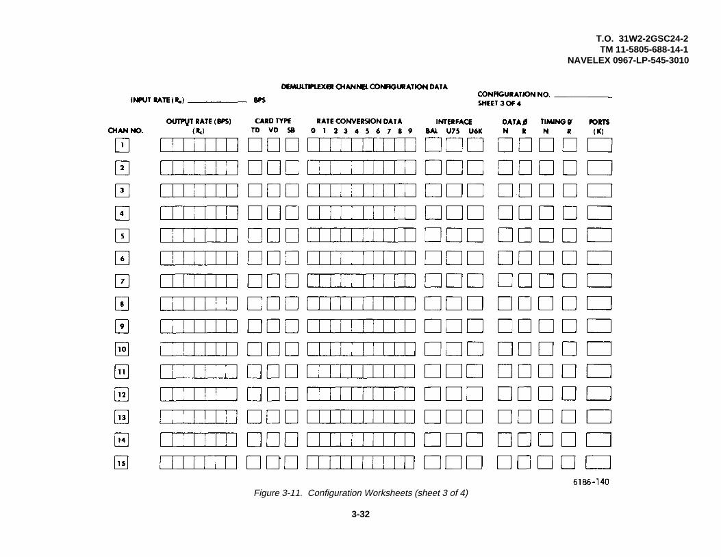
T.O. 31W2-2GSC24-2TM 11-5805-688-14-1
NAVELEX 0967-LP-545-3010
Figure 3-11. Configuration Worksheets (sheet 3 of 4)
3-32

T.O. 31W2-2GSC24-2TM 11-5805-688-14-1
NAVELEX 0967-LP-545-3010
Figure 3-11. Configuration Worksheets (sheet 4 of 4).
3-33

T.O. 31W2-2GSC24-2TM 11-5805-688-14-1
NAVELEX 0967-LP-545-3010
Figure 3-12. RCB Card - Switch Location Diagram
3-34

T.O. 31W2-2GSC24-2TM 11-5805-688-14-1
NAVELEX 0967-LP-545-3010
RD, and compare this value (KRp) with the channel’sinput data rate (Rc).
6. If Rc is equal to KRp (Rc = KRp), set S3 to the RCBposition, which completes the RCB card setup process.If Rc is less than KRp (Rc < KRp), set S3 to the URCposition and perform steps 7 through 9.
NOTE
In cases where Rc < KRp, coarse rateconversion of Rc to KRp must beperformed by the multiplexer. Toenable this conversion, a fill bit valuemust be computed and set into theRCB by 10-position switch S2.
7. Determine the quantity of fill bits required, using theexpression:
Fill bits = 899K (1 - Rc )KRp
where
K = quantity of ports assigned to the channel (fromworksheet)
Rc= channel data rate (from worksheet)
Rp = port rate (from worksheet).
NOTE
To ensure a proper computation of fillbit quantity, the value of 1 - Rc/KRpmust be determined to seven decimalplaces. Overall fill bit quantity, whencomputed, should be rounded to thenearest whole number; i.e., 316.7 isrounded to 317,
etc. The largest number of fill bitsthe multiplexer can process is 868. Ifthe computed quantity of fill bitsexceeds this value, a check forcomputational errors is suggested. Acorrectly computed fill bit valuegreater than 868 is indicative ofincorrect configuration data on theworksheet.
8. Refer to table 3-3 and locate the fill bit quantitycomputed in step7. Enter the 10-digit binary number associated with thisquantity in the RATE CONVERSION DATA block onsheet 1 of the worksheets.
NOTE
In step 9, ensure that the 10-digitnumber is inserted properly and the 0and 9 positions are not inadvertentlyreversed. Removal of all switchjumpers prior to starting the numberentry process is suggested.
9. Set 10-digit switch S2 on the RCB card toreflect the 10-digit binary number recorded on theworksheet, This completes the RCB card setup process.
10. Install the RCB card in its appropriate slot (1through 15) in the MULTIPLEXER row.
3-70. TE/TR CARD (P/N 61864060). For each channelthat uses a TE/TR card, set up the card as follows (referto figure 3-13 for all switch locations):
1. Note the channel INTFC 75 or 6K block on theworksheet; set S4 to the indicated 75 or 6K position.
2. Set S6 and S7 to the NORM position.
3-35

T.O. 31W2-2GSC24-2TM 11-5805-688-14-1
NAVELEX 0967-LP-545-3010
Figure 3-13. TE/TR Card - Switch Location Diagram
3. Set S8 to the NORM position.
NOTE
Failure to set S8 to the NORMposition will inhibit the display of anyerrors detected by the TE/TR carddiagnostic circuits.
4. Refer to sheet 1 of the worksheets and note ifthe CARD TYPE TE/TR block is marked TE or TR. Setcard switches S1, S2, and S3 to the indicated TE or TR
position. If S1, S2, and S3 are set to the TE position,proceed to step 5. If S1, S2, and S3 are set to the TRposition, proceed to step 6.
5. Multiply the number of ports (K) assigned tothe channel as indicated on sheet 1 and the port rate(Rp) entered on sheet 2 of the worksheets. Divide theproduct (KRp) by 3, and set S5 on the TE/TR card to thecomputed KRp/3 value. This completes the setup of theTE/TR card for the TE mode of operation.
3-36

T.O. 31W2-2GSC24-2TM 11-5805-688-14-1
NAVELEX 0967-LP-545-3010
NOTE
The computed KRp/3 value mustexactly match one of the six settingsof S5. If a match is not obtained, acheck of the computation issuggested. A correct computationnot yielding a match with one of thesettings of S5 indicates incorrectconfiguration data on the worksheet.
6. Set S9 to the channel data rate listed on theworksheet. This completes the setup of the TE/TR cardfor the TR mode of operation.
7. Install the TE/TR card in the appropriate slot(1 through 15) in the MULTIPLEXER row.
3-71. VE CARD (P/N 61864070). No setup of the VEcard is required. Install a VE card in the appropriate slotin the MULTIPLEXER row for each voice channel inputlisted on the worksheet.
3-72. MULTIPLEXER COMMON ELECTRONICSSETUP PROCEDURES.
3-73. Procedures for configuring the cards comprisingthe common electronics portion of the multiplexer areprescribed in paragraphs 3-74 through 3-77. Theinformation necessary to perform these procedures iscontained on sheet 2 of the configuration worksheets(figure 3-11).
3-74. RT CARD (P/N 61864150). The RT card islocated in slot 16 of the MULTIPLEXER row. Set up thecard as follows (refer to figure 3-14 for all switchlocations):
1. Refer to the OUTPUT INTERFACE BAL, U75,and U6K block on sheet 2 of the configurationworksheets, and set switches S2E and S8E to theindicated position.
2. If the OUTPUT INTERFACE BAL block ismarked, set switches S2A, S2B, S2C, S2D, S8A, S8B,S8C, and S8D to the B position. If the OUTPUTINTERFACE U75 or 6K block is marked, set theswitches to the U position.
3. Set both jumpers of switch S7 to the N(normal) or R (reversed) position as indicated in theDATA Ø N or R block on the worksheet.
4. Set both jumpers of switch S1 to the N(normal) or R (reversed) position as indicated in theTIMING Ø N or R block on the worksheet.
5. Set S3 to the 0 position.
6. Refer to the TIMING section on the worksheet,and note which TIMING SOURCE block (INT or EXT) ismarked. Set S5 to the indicated position. If S5 is set tothe EXT position, proceed to step 14.
NOTE
Row 1 of table 3-4 is applicable onlyto the RT card fitted with an oscillatorwhose output frequency is 9, 830, 400Hz. In such cases, proceed to step 7.When an oscillator of a differentfrequency is used, and the desired Ro
value appears in other than row 1 oftable 3-4, perform the procedures insteps 8, 9, and 10. If the desired Ro
value is not listed in table 3-4,perform the procedures in steps 11and 12.
7. Refer to row 1 of table 3-4, and locate theoutput rate (Ro) value entered on sheet 2 of theworksheets. Set S6 on the RT card to the positioncorresponding to the column of table 3-4 in which thedesired Ro value appears. Proceed to step 13.
3-37

T.O. 31W2-2GSC24-2TM 11-5805-688-14-1
NAVELEX 0967-LP-545-3010
Figure 3-14. RT Card - Switch Location Diagram
8. Determine the row and column of table 3-4 inwhich the desired Ro value is located
9. Determine the basic frequency of theoscillator (Y1) installed on the RT card.
10. Starting with the column of table 3-4 in whichthe desired Ro value is located, count that column andthe
3-38

T.O. 31W2-2GSC24-2TM 11-5805-688-14-1
NAVELEX 0967-LP-545-3010
Table 3-4. Reference Timer Rate Selection Data
ColumnRow 1 2 3 4 5 6 7 81 9,830,400 4,915,200 2,457,600 1,228,800 614,400 307,200 153,600 76,8002 9,523,200 4,761,600 2,380,800 1,190,400 595,200 297,600 148,800 74,4003 9,216,000 4,608,000 2,304,000 1,152,000 576,000 288,000 144,000 72,0004 8,908,800 4,454,400 2,227,200 1,114,600 556,800 278,400 139,200 69,6005 8,601,600 4,300,800 2,150,400 1,075,200 537,600 268,800 134,400 67,2006 8,294,400 4,147,200 2,073,600 1,036,800 518,400 259,200 129,600 64,8007 7,987,200 3,993,600 1,996,800 998,400 499,200 249,600 124,800 62,4008 7,680,000 3,840,000 1,920,000 960,000 480,000 240,000 120,000 60,0009 7,372,800 3,686,400 1,843,200 921,600 460,800 230,400 115,200 57,60010 7,065,600 3,532,800 1,766,400 883,200 441,600 220,800 110,400 55,20011 6,758,400 3,379,200 1,689,600 844,800 422,400 211,200 105,600 52,80012 6,451,200 3,225,600 1,612,800 806,400 403,200 201,600 100,800 50,40013 6,144,000 3,072,000 1,536,000 768,000 384,000 192,000 96,000 48,00014 5,836,800 2,918,400 1,459,200 729,600 364,800 182,400 91,200 45,60015 5,529,600 2,764,800 1,382,400 691,200 345,600 172,800 86,400 43,20016 5,222,400 2,611,200 1,305,600 652,800 326,400 163,200 81,600 40,80017 4,915,200 2,457,600 1,228,800 614,400 307,200 153,600 76,800 38,400
ColumnRow 9 10 11 12 13 14 15 161 38,400 19,200 9,600 4,800 2,400 1,200 600 3002 37,200 18,600 9,300 4,650 2,325 1162.5 581.25 290.6253 36,000 18,000 9,000 4,500 2,250 1125 562.5 281.254 34,800 17,400 8,700 4,350 2,175 1087.5 543.75 271,8755 33,600 16,800 8,400 4,200 2,100 1050 525 262.56 32,400 16,200 8,000 4,050 2,075 1037.5 518.75 259.3757 31,200 15,600 7,800 3,900 1,950 975 487.5 243.758 30,000 15,000 7,500 3,750 1,875 937.5 468.75 243.3759 28,800 14,400 7,200 3,600 1,800 900 450 22510 27,600 13,800 6,900 3,450 1,725 862.5 431.25 215.62511 26,400 13,200 6,600 3,300 1,650 825 412.5 206.2512 25,200 12,600 6,300 3,150 1,575 787.5 393.75 196.87513 24,000 12,000 6,000 3,000 1,500 750 375 187.514 22,800 11,400 5,700 2,850 1,425 712.5 356.25 178.12515 21,600 10,800 5,400 2,700 1,350 675 337.5 168.7516 20,400 10,200 5,100 2,550 1,275 637.5 318.75 159.37517 19,200 9,600 4,800 2,400 1,200 600 300 150
Change 2 3-39

T.O. 31W2-2GSC24-2TM 11-5805-688-14-1
NAVELEX 0967-LP-545-3010
columns to the left of that column, on the same row, untilthe column containing the installed oscillator’s frequencyis reached. Set S6 on the RT card to the number ofcolumns counted. For example, assume that an Ro of120, 000 bps (row 8, column 7) is desired and the RTcard is fitted with an oscillator whose output frequency is1, 920, 000 Hz (row 8, column 3). Starting with column 7and counting left through column 3 gives a count of 5 (7,6, 5, 4, 3). The number 5 would then be set into S6 ofthe RT card. Proceed to step 13.
11. Note the frequency of the oscillator installedon the RT card, and divide this frequency by the desiredRo. The result of this computation must be of the form 2n
(n = 0, 1, 2, 4 ....); otherwise, the desired Ro cannot beobtained with the oscillator.
12. Locate the computed OSC FREQ/Ro(oscillator frequency divided by (Ro) value in table 3-5,and set S6 on the RT card to the position indicated in thetable. For example, if the RT card oscillator frequency is4, 800, 000 Hz, and the desired Ro is 600, 000 bps, thenOSC FREQ/Ro = 8. As shown in table 3-5, the propersetting for S6 is position 4.
13. This completes the setup procedure for RTcards operating from an internal timing source (S5 set toINT). Install the RT card in slot 16 of the MULTIPLEXERrow.
14. Set S4 to the 75 or 6K position as indicated inthe INPUT INTFC 75 or 6K block on sheet 2 of theconfiguration worksheets.
15. Determine the frequency of the externaltiming source being supplied to the multiplexer from theEXT FREQ HZ block on the worksheet, and divide thisfrequency by the output rate (Ro) entered
in the OUTPUT RATE (Ro) BPS block of the TIMINGsection. The result of this computation must be of the 2n
form (n = 0, 1, 2, 4 ...); otherwise, the input frequencybeing supplied will not yield the desired Ro.
16. Locate the value computed in step 15 in theOSC FREQ/Ro column of table 3-5, and set S6 on theRT card to the corresponding position indicated in thetable. This completes the setup of an RT card operatingfrom an external reference timing source (S5 set toEXT).
Table 3-5. Reference Timer Setup Data
OSC FREQ/Ro S6 Setting
1 12 24 38 416 532 664 7128 8256 9512 101024 112048 124096 138192 1416384 1532768 16
3-40

T.O. 31W2-2GSC24-2TM 11-5805-688-14-1
NAVELEX 0967-LP-545-3010
17. Install the RT card in slot 16 of theMULTIPLEXER row.
3-75. OEG CARD (P/N 61864020). The OEG card islocated in slot 19 of the MULTIPLEXER row. To set upthis card, set each of the 15 jumpers of S1 to the ONposition (figure 3-15).
NOTE
Each position of S1 corresponds to asimilarly numbered multiplexer channel.Setting any of the S1 jumpers to theOFF position inhibits display of thechannel card’s diagnostic error statuswhen the multiplexer set is in the self-test mode of operation. Thisconfiguration also prevents the display oferrors detected on the card duringnormal operation. A jumper on S1should be set to the OFF position only inthose unusual cases when the affectedchannel is active but does not have achannel card installed.
3-76.SEQ CARD (P/N 61864040).The seq card islocated in slot 21 of the MULTIPLEXER row. Set up thecard as follows (refer to figure 3-16 for all switchlocations):
1. Refer to the PORT STRAPPING section onsheet 2 of the configuration worksheets. Set eachjumper of 31- position S1 to A (active) or S (strapped) asindicated.
NOTE
Depending upon the multiplexerconfiguration being implemented, the
total number of ports designated aseither A or S on the worksheet mayvary between 15 and 31. Thepositions of S1 jumpers for ports notdesignated as A or S on theworksheet are not important and canbe either A or S.
2. Refer to the worksheet, and count the total number ofports indicated as either A or S and ensure that thisquantity is the same as the quantity entered in thePORTS IN USE (N) block of the worksheet.
NOTE
If the total number of ports indicatedas either A or S does not exactlymatch the number entered in thePORTS IN USE (N) block, theinformation in the worksheet isincorrect.
3. Refer to table 3-6 and locate the numberentered in the PORTS IN USE (N) block of theworksheet. Set the corresponding 5-digit binary numberlisted in the table into switch S2 of the seq card. Thiscompletes the setup of the seq card.
NOTE
Ensure that the MSB and LSBpositions of the 5- digit binarynumber are not inadvertentlyreversed; i.e., the LSB digit of table 3-6 must be set into S2 position A, andthe MSB digit of table 3-6 must be setinto S2 position E.
4. Install the seq card in slot 21 of theMULTIPLEXER row.
3-41

T.O. 31W2-2GSC24-2TM 11-5805-688-14-1
NAVELEX 0967-LP-545-3010
Figure 3-15. OEG Card - Switch Location Diagram
3-42

T.O. 31W2-2GSC24-2TM 11-5805-688-14-1
NAVELEX 0967-LP-545-3010
Figure 3-16. Seq Card - Switch Location Diagram
3-43

T.O. 31W2-2GSC24-2TM 11-5805-688-14-1
NAVELEX 0967-LP-545-3010
Table 3-6. Seq Card Ports-in-Use Switch Settings
Ports in S2 SettingsUse (N) LSB MSB
A B C D E15 1 1 1 1 016 0 0 0 0 117 1 0 0 0 118 0 1 0 0 119 1 1 0 0 120 0 0 1 0 121 1 0 1 0 122 0 1 1 0 123 1 1 1 0 124 0 0 0 1 125 1 0 0 1 126 0 1 0 1 127 1 1 0 1 128 0 0 1 1 129 1 0 1 1 130 0 1 1 1 131 1 1 1 1 1
3-44

T.O. 31W2-2GSC24-2TM 11-5805-688-14-1
NAVELEX 0967-LP-545-3010
3-77. GC/DM CARD (P/N 61864030). Ensure that aGC/DM card is installed in slot 20 of the MULTIPLEXERrow. No setup procedures are required for this card.
3-78. DEMULTIPLEXER CHANNEL ELECTRONICSSETUP PROCEDURES.
3-79. Paragraphs 3-80 through 3-83 prescribe the setupprocedures for the demultiplexer channel cards. Theinformation required for the setup process is containedon sheet 3 of the configuration worksheets (figure 3-11).
3-80.SB CARD (P/N 61864090).For each channel thatuses an SB card, set up the card as follows (refer tofigure 3-17 for all switch locations):
NOTE
SB cards are used for each channelmarked with an X in the CARD TYPESB block of the worksheet. If theCARD TYPE SB block is marked withthe letters NB, a narrow bandsmoothing buffer (NBSB) card (P/N61864160) is used. Procedures forthe NBSB card setup are presented inparagraph 3-81.
1. Note the demultiplexer input rate (Ro) valueentered on the worksheet. If Ro is less than 2000 bps,set S1 to the Ro < 2KHZ position. If Ro is 2000 bps orgreater, set S1 to the Ro > 2KHZ position.
2. Set S9 to the NORM position.
3. Set S4 to the ON position.
NOTE
Setting S4 to the OFF position willinhibit the display of any card errorsdetected by the SB card diagnosticcircuits.
4. Refer to the DATA Ø N or R block of theworksheet, and set both jumpers of S10 to the indicatedN (normal) or R (reversed) position.
5. Refer to the TIMING Ø N or R block of theworksheet, and set both jumpers of S11 to the indicatedN (normal) or R (reversed) position.
6. Refer to the INTERFACE BAL, U75, or U6Kblock of the worksheet, and set S19 and S22 to theindicated B (balanced), U75 (unbalanced 75 ohms), orU6K (unbalanced 6K ohms) position.
7. If the INTERFACE BAL block of the worksheetis marked, set S14 through S18, S20, S21, and S23 tothe B position. If the INTERFACE U75 or U6K block ismarked, set the switches to the U position.
8. Refer to the worksheet, and note the channel'soutput data rate value entered in the OUTPUT RATE(BPS) (Rc) block.
9. Set S5 on the SB card to one of the fourcorresponding positions on the board for the family ofrate ranges in which the listed channel data rate falls. Asan example, if the desired channel data rate is 48000(48K), S5 would be set to the B position as indicated bythe switch position markings for switch S5. As shown onthe SB card, the B rate range is for rates from 47 kbpsthrough 94 kbps, and thus
3-45

T.O. 31W2-2GSC24-2TM 11-5805-688-14-1
NAVELEX 0967-LP-545-3010
Figure 3-17. SB Card - Switch Location Diagram
3-46

T.O. 31W2-2GSC24-2TM 11-5805-688-14-1
NAVELEX 0967-LP-545-3010
includes the 48-kbps channel rate desired.
10. Note the rate range (A, B, C, or D) selectedin step 9 and set S7 to the corresponding position. Forexample, if range B was selected, S7 would be set to theB, C, D position. If range A was selected, 57 would beset to the A position.
11. Set S8 to the rate range selected in step 9.
12. Set S24 to the rate range selected in step 9.
13. Set S25 to the rate range selected in step 9.
NOTECertain positions of S12 indicate rateranges A’ (A prime) and B’ (B prime).When S5 is set to the A range and thechannel rate (Rc) listed on theworksheet is 1.5 Mbs or greater, S12must be set to the A’ position. Forchannel rates in the A range whichare below 1.5 Mbs, and for anychannel rate in the B range, the A’and B’ positions of S12 are used incases where the multiplexer’schannel output smoothing interval isunacceptable to user sinkinstruments. In such cases, specialinstructions will be added to theconfiguration worksheets.Discussion pertaining to selectionand use of S12 A’ and B’ ranges iscontained in paragraph 3-58.
14. Set S12 to the rate range selected in step 9or as instructed in the above note.
15. Refer to sheet 3 of the worksheets, and notein the PORTS K blocks the number of ports (K) assignedto each channel. Note the port rate
(Rp) shown on sheet 4 of the worksheets. Multiply Kand Rp, and compare this value (KRp) with the channel’soutput data rate (Rc).
16. If Rc is equal to KRp (Rc = KRp), set S3 to theSB position, which completes the SB card setup process.Install the SB card in its appropriate slot (1 through 15) inthe DEMULTIPLEXER row. If Rc is less than KRp (Rc <KRp), set S3 to the URD position and perform steps 17through 19.
NOTE
In cases where Rc < KRp, coarse rateconversion of KRp to Rc must beperformed by the demultiplexer. Toenable this conversion, a fill bit valuemust be computed and set into theSB by 10-position switch S2.
17. Determine the quantity of fill bits required,using the expression:
Fill bits = 899K (1 - Rc )KRp
whereK = quantity of ports assigned to the channel (fromworksheet)
Rc = channel data rate (from worksheet)
Rp = port rate (from worksheet).
NOTE
To ensure a proper computation of fillbit quantity, the value of 1 - Rc/KRpmust be determined to seven decimalplaces. Overall fill bit quantity, whencomputed, must be rounded to thenearest whole number; i.e., 316.7 isrounded to 317, etc. The largestnumber of
Change 2 3-47

T.O. 31W2-2GSC24-2TM 11-5805-688-14-1
NAVELEX 0967-LP-545-3010
fill bits the demultiplexer can processis 868. If the computed quantity of fillbits exceeds this value, a check forcomputational errors is suggested. Acorrectly computed fill bit valuegreater than 868 is indicative ofincorrect configuration data on theworksheet.
18. Refer to table 3-3, and locate the fill bitquantity computed in step 17. Enter the 10-digit binarynumber associated with this quantity in the RATECONVERSION DATA block on sheet 3. of theworksheets.
NOTE
In step 19, ensure that the 10-digitnumber is inserted properly and the 0and 9 positions are not inadvertentlyreversed. Removal of all switchjumpers prior to starting the numberentry process is suggested.
19. Set 10-digit switch S2 on the SB card to reflect the10-digit binary number recorded on the worksheet. Thiscompletes the SB card setup process.
20. Install the SB card in its appropriate slot (1 through15) in the DEMULTIPLEXER row.
3-81. NBSB CARD (P/N 61864160). For each channelthat uses an NBSB card, set up the card as follows (referto figure 3-18 for all switch locations):
NOTE
NBSB cards are used for eachchannel marked with the letters NB inthe CARD TYPE SB block of sheet 3of the worksheets. If the CARD TYPESB block is
marked with an X, a smoothing buffer(SB) card (P/N 61864090) is used.Procedures for SB card setup arepresented in paragraph 3-80.
1. Note the demultiplexer input rate (Ro) value enteredon the worksheet. If Ro is less than 2000 bps, set S1 tothe RO < 2KHZ position. If Ro is 2000 bps or greater, setS1 to the RO > 2KHZ position.
2. Set S9 to the NORM position.
3. Set S4 to the ON position.
NOTE
Setting S4 to the OFF position willinhibit the display of any card errorsdetected by the NBSB carddiagnostic circuits.
4. Refer to the DATA Ø N or R block on the worksheet,and set both jumpers of S10 to the indicated N (normal)or R (reversed) position.
5. Refer to the TIMING Ø N or R block of the worksheetand set both jumpers of S11 to the indicated N (normal)or R (reversed) position,
6. Refer to the INTERFACE BAL, U75, or U6K block ofthe worksheet, and set S19 and S22 to the indicated B(balanced) U75 (unbalanced 75 ohms) or U6K(unbalanced 6K ohms) position.
7. If the INTERFACE BAL block of the worksheet ismarked, set S14, S15, S16, S17, 518, S20, S21, andS23 to the B position. If the INTERFACE U75 or U6Kblock is marked, set the switches to the U position.
8. Refer to the worksheet, and note the channel's output(data rate
3-48
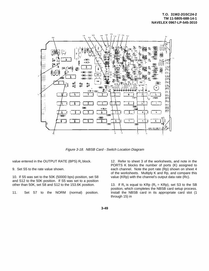
T.O. 31W2-2GSC24-2TM 11-5805-688-14-1
NAVELEX 0967-LP-545-3010
Figure 3-18. NBSB Card - Switch Location Diagram
value entered in the OUTPUT RATE (BPS) Rc block.
9. Set S5 to the rate value shown.
10. If S5 was set to the 50K (50000 bps) position, set S8and S12 to the 50K position. If S5 was set to a positionother than 50K, set S8 and S12 to the 153.6K position.
11. Set S7 to the NORM (normal) position.
12. Refer to sheet 3 of the worksheets, and note in thePORTS K blocks the number of ports (K) assigned toeach channel. Note the port rate (Rp) shown on sheet 4of the worksheets. Multiply K and Rp, and compare thisvalue (KRp) with the channel’s output data rate (Rc).
13. If Rc is equal to KRp (Rc = KRp), set S3 to the SBposition, which completes the NBSB card setup process.Install the NBSB card in its appropriate card slot (1through 15) in
3-49

T.O. 31W2-2GSC24-2TM 11-5805-688-14-1
NAVELEX 0967-LP-545-3010
the DEMULTIPLEXER row. If Rc is less than KRp (RC <KRp), set S3 to the URD position and perform steps 14through 16.
NOTE
In cases where Rc < KRp, coarse rateconversion of KRp to Rc must beperformed by the demultiplexer. Toenable this conversion, a fill bit valuemust be computed and set into theNBSB by 10-position switch S2.
14. Determine the quantity of fill bits required, using theexpression:
Fill bits = 899K (1 - Rc--)KRp
where
K = quantity of ports assigned to the channel (fromworksheet)
Rc = channel data rate (from worksheet)
Rp = port rate (from worksheet)
NOTE
To ensure a proper computation of fillbit quantity, the value of 1 - Rc/KRpmust be determined to seven decimalplaces. Overall fill bit quantity, whencomputed, should be rounded to thenearest whole number; i.e., 316.7 isrounded to 317, etc. The largestnumber of fill
bits the demultiplexer can process is868. If the computed quantity of fill bitsexceeds this value, a check forcomputational errors is suggested. Acorrectly computed fill bit value greaterthan 868 is indicative of incorrectconfiguration data on the worksheet.
15. Refer to table 3-3 and locate the fill bit quantitycomputed in step 14. Enter the 10-digit binary numberassociated with this quantity in the RATE CONVERSIONDATA block on sheet 3 of the worksheets.
NOTE
In step 16, ensure that the 10-digitnumber is inserted properly and the 0and 9 positions are not inadvertentlyreversed. Removal of all switchjumpers prior to starting the numberentry process is suggested.
16. Set 10-digit S2 on the NBSB card to reflect the 10-digit binary number entered on the worksheet. Thiscompletes the NBSB card setup process.
17. Install the NBSB card in its appropriate slot (1through 15) in the DEMULTIPLEXER row.
3-82. VD CARD (P/N 61864140). No setup of the VDcard is required. Install a VD card in the appropriate slotin the DEMULTIPLEXER row indicated on theworksheet.
3-83. TD CARD (P/N 61864130). Set up the TD card asfollows (refer to figure 3-19 for all switch locations):
1. Set S1 to the ON position.
3-50

T.O. 31W2-2GSC24-2TM 11-5805-688-14-1
NAVELEX 0967-LP-545-3010
Figure 3-19. TD Card - Switch Location Diagram
NOTE
Setting S1 to the OFF positioninhibits the display of errors detectedby the TD diagnostic circuits.
2. Set S2 to the N (normal) position.
3. Refer to the DATA 0 N or R block on the worksheet,and set S5 to
the indicated N (normal) or R (reversed) position.
4. Refer to the INTERFACE BAL, U75, or U6K block onthe worksheet. If the INTERFACE BAL block is marked,set S6A, S6B, S6C, and S6D to the B position. If theINTERFACE U75 or U6K is marked, set the switches tothe U position.
5. Multiply the number of ports (K) assigned to thechannel on sheet
3-51

T.O. 31W2-2GSC24-2TM 11-5805-688-14-1
NAVELEX 0967-LP-545-3010
3 and the port rate (Rp) listed on sheet 4 of theworksheet. Divide the product (KRp) by 3, and set S4 onthe TD card to the range that includes the computedKRp/3 value. This completes the TD card setupprocess.
NOTE
The computed KRp/3 value mustexactly match one of the six rangeslisted on switch S4. If a match is notobtained, a check of the computationis suggested. A correct computationnot yielding a match with one of theS4 ranges indicates incorrectconfiguration data on the worksheet.
6. Install the TD card in its appropriate slot (1 through15) in the DEMULTIPLEXER row.
3-84. DEMULTIPLEXER COMMON ELECTRONICSSETUP PROCEDURES.
3-85. The information required for configuring the cardscomprising the common electronics section of thedemultiplexer is contained on sheet 4 of the configurationworksheets (figure 3-11). Based on this information,paragraphs 3-86 through 3-90 prescribe the proceduresto be used in the setup process.
3-86. OEG CARD (P/N 61864020). The demultiplexerand multiplexer OEG cards are identical, and are locatedin slot 19 of the MULTIPLEXER and DEMULTIPLEXERrows. Procedures for setting up the demultiplexer OEGcard are the same as those prescribed in paragraph 3-75for the multiplexer OEG card.
3-87. SEQ CARD (P/N 61864040), The demultiplexerseq card in slot 21 of the DEMULTIPLEXER row isidentical to that used in the multiplexer. Procedures to
set up this card are identical to those prescribed inparagraph 3-76, with the following exceptions: (1)worksheet information pertinent to the demultiplexer seqcard is contained on sheet 4 of the configurationworksheets; and (2) the demultiplexer seq card isinstalled in slot 21 of the DEMULTIPLEXER row.
3-88. GC/DM CARD (P/N 61864030). Thedemultiplexer GC/DM card is identical to that used in themultiplexer. Ensure that a GC/DM card is installed in slot20 of the DEMULTIPLEXER row. No setup proceduresare required for this card.
3-89. FS CARD (P/N 61864110). The FS card islocated in slot 16 of the DEMULTIPLEXER row. Set upthe FS card as follows (refer to figure 3-20 for all switchlocations):
1. Refer to sheet 4 of the configuration worksheets andnote the DATA Ø N or R block. Set S1 to the indicated N(normal) or R (reversed) position.
2. Refer to the TIMING Ø N or R block on theworksheet, and set S2 to the indicated N (normal) or R(reversed) position.
3. Set S3A and S3B to the NORM position.
4. Refer to the INTFC 75 or 6K block on the worksheet,and set S4 and S5 to the indicated 75 or 6K position.install the FS card in slot 16 of the DEMULTIPLEXERrow.
3-90. ERD CARD (P/N 61864120). The ERD card islocated in slot 17 of the DEMULTIPLEXER row, To setup the ERD card, refer to the ERROR RATETHRESHOLD block on sheet 4 of the configurationworksheets, and set S1 (figure 3-21) to the indicatedposition. Install the ERD card in slot 17 of theDEMULTIPLEXER row.
3-52

T.O. 31W2-2GSC24-2TM 11-5805-688-14-1
NAVELEX 0967-LP-545-3010
Figure 3-20. FS Card - Switch Location Diagram
3-91. DISPLAY CARD (P/N 61864050)SETUP PROCEDURES.
3-92. The display card is located in slot 22 of theMULTIPLEXER row. Set up the display card as follows:
1. If both the multiplexer and demultiplexer portions ofthe multiplexer set are being used, i.e., overallconfiguration is duplex (paragraph 3-7), set S1 (figure 3-22) to the NORM position.
2. If either the multiplexer or the demultiplexer portion ofthe multiplexer set is not being used, set S1
to the MUX OFF or DEMUX OFF position as applicable.This will inhibit diagnostic error indications from theportions of the multiplexer set not being used. Install thedisplay card in slot 22 of the DEMULTIPLEXER row.
3-93. THERMAL ALARM OPTIONS.
3-94.The multiplexer set has alarm circuits that activatewhen the operating temperature within the set exceedsspecified limits. Upon activation, the alarm circuits areset up to perform one of the two following optionalfunctions: (1) light the front panel TEMPERATUREindicator, cause a remote alarm indication to appear atconnector
3-53

T.O. 31W2-2GSC24-2TM 11-5805-688-14-1
NAVELEX 0967-LP-545-3010
Figure 3-21.ERD Card - Switch Location Diagram
3-54

T.O. 31W2-2GSC24-2TM 11-5805-688-14-1
NAVELEX 0967-LP-545-3011
Figure 3-22. Display Card - Switch Location Diagram
J66, and cause the multiplexer set power supply toautomatically shut down; and (2) light the front panelTEMPERATURE indicator and cause a remote alarmindication to appear at connector J66.
3-95. In option 1, the multiplexer set ceases to processinput/output data until the cause of the overtemperaturesituation is corrected. The multiplexer set is initiallymanufactured with option 1 installed.
Dangerous voltages are presentwithin the front
panel. Turn multiplexer poweroff and disconnect power cordfrom power source beforeremoving front panel assembly.
3-96. If option 2 is desired, remove power, removethe front panel assembly (paragraph 6-23), andcarefully remove the bare wire jumper solderedbetween terminals E24 and E25 of front panelboard A2A1 (P/N 61861028) (refer to figure 3-23 forterminal locations). Option 1 can be reinstalled bysoldering a jumper between terminals E24 and E25.
Change 1 3-55

T.O. 31W2-2GSC24-2TM 11-5805-688-14-1
NAVELEX 0967-LP-545-3011
3-96.1. REMOTE ALARM OPTIONS
3.96.2. There are seven remote alarm signals routed tothe REMOTE ALARM connector on the rear panel. Theremote alarm signals that are applied to the REMOTEALARM connector are initiated by the multiplexer setdiagnostic circuits. The diagnostic circuits automaticallymonitor the equipment for faulty system data inputs andmultiplexer set equipment malfunctions. Each of theremote alarm signals is associated with a pair of outputs(C1 and C2) that are held in an open-circuit condition in ano-error condition. When a fault is detected, theassociated pair of outputs is closed in the multiplexer setto produce a closed-loop output condition. The sevenremote alarm signals and their associated output pinlocations on the REMOTE ALARM connector are listedbelow. Connector kit assembly 61867000-009 or6187000-019 contains the mating connector for theREMOTE ALARM connector.
Signal Pin No. Function
LOFAC1 J66A System indicator - ProLOFAC2 J66B duces fault indication
during time thatdemultiplexer circuitsare not synchronizedwith incoming data.
LOFBC1 J66-C System indicator - ProLOFBC2 J66-D duces a continuing
fault indication oncedemultiplexer circuitsare not synchronizedwith incoming data.Fault indication re-mains until DISPLAYRESET switch ispressed onmultiplexer set.
LERRC1 J66-G System indicator - Pro
Signal Pin No. Function
LERRC2 J66-H duces fault indicationduring time that biterror rate in ademultiplexer exceedsa preselectedthreshold.
OOTC1 J66-N System indicator - Pro-OOTC2 J66-P duces fault indication
when an out-oftolerance conditionexists between theincoming data and onemultiplexer inputcircuit.
FAILC1 J66-E Multiplexer set indica-FAILC2 J66-F tor - Produces fault
indication when a cardmalfunction inmultiplexer set isdetected.
PSFC1 J66-L Multiplexer set indica-PSFC2 J66-M tor Produces fault
indication when powersupply malfunction inmultiplexer set isdetected.
TEMPC1 J66-J Multiplexer set indica-TEMPC2 366-K tor Produces fault
indication wheninternal operatingtemperature inmultiplexer setexceeds 205°F(96°C).
3-97. MULTIPLEXER SET OPERATIONALTESTS.
3-98. When a multiplexer set is reconfigured for a differentsystem application, the performance standards prescribedin paragraph 6-38 will be performed. These procedureswill also be performed when a multiplexer set is initiallyinstalled in a system to ensure that the equipment isoperationally ready to perform its assigned tasks.
Change 1 3-56

T.O. 31W2-2GSC24-2TM 11-5805-688-14-1
NAVELEX 0967-LP-545-3011
Figure 3-23. Front Panel Printed Circuit Card - Jumper Location Diagram3-57

T.O. 31W2-2GSC24-2TM 11-5805-688-14-1
NAVELEX 0967-LP-545-3011
SECTION IV
PREPARATION FOR RESHIPMENT
3-99. GENERAL.
3-100. This section contains instructions for preparingthe multiplexer set for shipment. The original shippingcontainer, padding, and filler should be used for packingthe multiplexer set for shipment.
3-101. PACKING PROCEDURES,
The multiplexer setweighs 140 pounds. Use amechanical lifting devicewhenever possible. Toprevent injury topersonnel, it isrecommended that aminimum of four men beused when a multiplexerset is to be liftedmanually.
1. Set POWER CONTROL switch to OFF.
NOTE
Perform the procedures insteps 2 through 10 when themultiplexer set is rackmounted and uses theextendable slides forsupport. Proceed to step 11when the multiplexer set issecured to a rack only by itstwo rack-mounting flanges.When the multiplexer set isinstalled on a flat surfacesuch as a bench or table,perform only steps 4, 5, 9,and 10 below.
2. Remove and retain 12 screws and washerssecuring two rack-mounting flanges to electronicequipment rack.
3. Carefully extend multiplexer set upon itsmounting slides until slides lock in extended position.
4. Disconnect power cable from primary powersource and from multiplexer set.
5. Disconnect remote alarms cable frommultiplexer set, and disconnect all input/output data andtiming signal cables.
6. Release the extender slide locks and carefullyremove multiplexer set from rack. Place multiplexer seton a suitable work bench or surface.
7. Remove two outer extender slide sectionssecured to electronic equipment rack. Retain allmounting hardware.
8. Install two outer extender slide sections removedin step 7 on two inner slide sections mounted on multi-plexer set.
9. Verify that all captive screws on front panel andtop panel of multiplexer set are securely fastened.
NOTE
When original shippingcontainer is not available, pre-pare multiplexer set for shipmentin accordance with currentlyapplicable packaginginstructions for electronicequipment.
10. Place multiplexer set and power cable inshipping container and prepare equipment for shipment.
Change 1 3-58

T.O. 31W2-2GSC24-2TM 11-5805-688-14-1
NAVELEX 0967-LP-545-3011
11. Disconnect power cable from primary powersource and from multiplexer et.
12. Disconnect remote alarms cable frommultiplexer set and disconnect all input/output data andtiming signal cables from multiplexer set.
13. Support multiplexer set as necessary andremove 12 screws and washers securing two rack-mounting flanges to electronic equipment rack. Retainmounting hardware.
14. Carefully move multiplexer set from rackand place multiplexer set on a suitable work bench orsurface.
15. Install pair of slide assemblies removedfrom multiplexer set at time of initial installation. Useseven screws on each slide assembly.
16. Verify that all captive screws on frontpanel and top panel of multiplexer set are securelyfastened.
17. Place multiplexer set and power cable inshipping container and prepare equipment for shipment.
Change 1 3-59

T.O. 31W2-2GSC24-2TM 11-5805-688-14-1
NAVELEX 0967-LP-545-3011
CHAPTER 4
OPERATION
4-1 INTRODUCTION.
4-2. When the multiplexer set is configured asprescribed in section I of chapter 3, the functionaloperation of the multiplexer is fully automatic. Theoperator requirements for operating the equipment arelimited to the application of operating power. Once theequipment is in operation, operator duties consist ofvisual checks of the automatic diagnostic error displaysand the performance of periodic maintenance tests.
4-3. CONTROLS AND INDICATORS.
4-4. All controls and indicators are mounted on the frontpanel of the multiplexer set. The controls and indicatorsare shown in figure 4-1. The controls and indicators,together with their functional descriptions, are listed intable 4-1.
4-5. OPERATING INSTRUCTIONS.
4-6. Paragraphs 4-7 through 4-10 contain the operatingprocedures for the multiplexer set; no unusual or specialoperating procedures are required. The lamp test andself-test procedures in paragraphs 4-8 and 4-9 can beperformed on an operational multiplexer set withoutdisrupting the functional operation of the equipment.
4-7. STARTING PROCEDURES.
1. Ensure that POWER CONTROL circuit breakeris pressed to its on position.
2. Set POWER CONTROL switch to ON. Observethat POWER CONTROL ON indicator is lighted. Otherindicators may also be lighted.
Figure 4-1. Front Panel Controls and Indicators
4-1

T.O. 31W2-2GSC24-2TM 11-5805-688-14-1
NAVELEX 0967-LP-545-3011
Table 4-1. Multiplexer Set Controls and Indicators
Controls/Indicators Function
POWER CONTROL switch Applies multiplexer set operating power.
POWER CONTROL ON indicator Lights when operating power is applied.
POWER CONTROL circuit breaker Provides equipment protection when electricaloverload occurs.
SYSTEM STATUS group
LOSS OF MUX TIMING indicator Lights when source of multiplexer referencetiming is removed. Remains lighted untilreset.
LOSS OF DEMUX TIMING indicator Lights when source of demultiplexer inputtiming is removed. Remains lighted untilreset.
LOSS OF FRAME A indicator Lights only when demultiplexer is notsynchronized with transmitting multi-plexer.
LOSS OF FRAME B indicator Also lights when demultiplexer is notsynchronized with transmitting multi-plexer, but remains lighted until reset.
LINK ERROR RATE indicator Lights when bit error rate applied todemultiplexer exceeds a predeterminedthreshold.
ALARMS group
POWER SUPPLY indicator Lights when a power supply malfunction isdetected.
TEMPERATURE indicator Lights when internal operating temperatureexceeds 205°F (96°C).
TEST CONTROL group
LAMP TEST switch When pressed, causes a test of all indicatorsexcept POWER CONTROL ON indicator(paragraph 4-8).
SELF TEST switch When set to on (up) position, initiatesa test of built-in diagnostic circuits(paragraph 4-9).
4-2

T.O. 31W2-2GSC24-2TM 11-5805-688-14-1
NAVELEX 0967-LP-545-3011
Table 4-1. Multiplexer Set Controls and Indicators (Cont)
Controls/Indicators Function
TEST CONTROL group (Cont)
DISPLAY RESET switch When pressed, extinguishes all lightedindicators except POWER CONTROL ONindicator.
FAULT LOCATION group
MULTIPLEXER CARD indicator Lights when a multiplexer card malfunctionis detected. Remains lighted until reset.
MULTIPLEXER OUT OF TOL indicator Lights when an out-of-tolerance conditionis detected on one or more input channels.
DEMULTIPLEXER CARD indicator Lights when a demultiplexer card malfunctionis detected. Remains lighted until reset.
FAULT LOCATION numerical display Functions are as follows:
a) When MULTIPLEXER CARD or DEMULTIPLEXER CARDindicator is lighted, displays numerical location ofmalfunctioning card.
b) When MULTIPLEXER OUT OF TOL indicator is lighted,
displays number of channel that is out of tolerance. Whentwo or more channels are out of tolerate at the same time,displays number of these channels sequentially.
c) When SELF TEST switch is in on (up) position and no
malfunction exists, displays 00. When SELF TEST switch isin on (up) position and a malfunction exists, displaysnumerical location of card whose diagnostic circuits aremalfunctioning.
4-3

T.O. 31W2-2GSC24-2TM 11-5805-688-14-1
NAVELEX 0967-LP-545-3011
NOTE
The time required for the multiplexerset to stabilize when the POWERCONTROL switch is set to the ONposition may take several minutes.Therefore, false error indications mayoccur when step 3 is performedbefore the multiplexer set hasstabilized.
3 Press and release DISPLAY RESET switch.Observe that all indicators except POWER CONTROLON indicator are out. When one or more indicators,other than POWER CONTROL ON indicator, are lighted,wait 60 seconds and repeat this step.
4-8. LAMP TEST PROCEDURES.
1. Press and hold LAMP TEST switch. Observethat all indicators are lighted. FAULT LOCATIONnumerical display is 88.
2. Release LAMP TEST switch. Observe thatall indicators except POWER CONTROL ON indicatorare out. FAULT LOCATION numerical display is out.
4-9. SELF-TEST PROCEDURES.
NOTEFor multiplexer output rates (Ro
above 10 kbps, the time required for afinal
display of the self-test results isapproximately 10 seconds. The timerequired for output rates less than 10kbps is estimated by using theexpression: time (in seconds) =90,000/Ro The time required for afinal display of the self-test results isapproximately 10 minutes for an Ro of155 bps.
1. Set SELF TEST switch to on (up) position.
2. Wait for completion of the self-test functionwithin the multiplexer set and then observe that allindicators are lighted and FAULT LOCATION numericaldisplay is 00.
3. Set SELF TEST switch to off (down) position.Observe that all indicators except POWER CONTROLON indicator are out.
4-10. STOPPING PROCEDURES.
1. Set POWER CONTROL switch to OFF.
2. Observe that all indicators are out.
4-11. EMERGENCY STOPPING PROCEDURES.
1. Set POWER CONTROL switch to OFF.
2. Observe that all indicators are out.
4-4

T.O. 31W2-2GSC24-2TM 11-5805-688-14-1
NAVELEX 0967-LP-545-3011
CHAPTER 5
THEORY OF OPERATION5-1. INTRODUCTION.
5-2. This chapter contains the principles of operationfor the circuits in the multiplexer set. The chapter isdivided into five sections. Section I contains discussionsof the output data message format and basic equipmentconcepts used in the multiplexer set. The overall blockdiagram discussions for the multiplexer, demultiplexer,and diagnostic functions are in section II. Section IIIcontains the block diagram discussions and detailedtheory of operation for the printed circuit cards in themultiplexer function. The block diagram discussions anddetailed theory of operation for the printed circuit cards inthe demultiplexer function are in section IV. Section Vcontains the block diagram discussions and detailedtheory of operation for the power supply.
5-3. The reference designations for major circuitcomponents, such as U1, Q5, etc, appear in thefunctional blocks in the block diagrams for the printedcircuit cards and power supply to assist in relating theblock diagram functional descriptions to the associateddetailed theory of operation discussions. The detailedtheory of operation discussions, in turn, reference thecircuit reference designations as they appear on theassociated logic diagrams or schematics in the circuitdiagrams manual. The use of logic symbols in the blockdiagrams is limited to simplified functional applicationsthat are best illustrated by the use of logic symbols.Complete logic circuits are not shown in the blockdiagrams.
5-4. In the detailed circuit discussions, certainconventions are used to describe and define logicelements. These conventions are described by thefollowing examples.
Example Description
U1, U2, Q5, The reference designationsetc. used in this manual are the
same as those that appearon schematics and logicdiagrams, and showphysical locations onequipment assemblydrawings.
U1-6, U2-4, Many microcircuit packagesetc. in this equipment contain
multiple circuits: four ANDgates, two shift registers,etc. Therefore, when one ormore circuits within onepackage need to beidentified, one of the input oroutput pins associated withthe specific circuit beingdiscussed is added to thereference designation foridentification. Normally, anoutput pin is used to identifya particular circuit.
MGCXX, DGCXX, All functional signals inMMFCX, DMFCX- the equipment are assigned
names. Initial letter Mindicates a multiplexersignal; initial letter Dindicates a demultiplexersignal. X or XX identifies aparticular signal within asignal family; for example,MGCXX consists of 15signals; MGCO1 throughMGC15. The bar signal "-"after a signal nameindicates that the signal islow in its true state.
5-1

T.O. 31W2-2GSC24-2TM 11-5805-688-14-1
NAVELEX 0967-LP-545-3011
SECTION I
MESSAGE FORMAT AND BASIC EQUIPMENT CONCEPTS
5-5. GENERAL.
Paragraphs 5-6 through 5-18 contain a description of themessage format used in the transmission of digital datafrom the multiplexer in a multiplexer set to thedemultiplexer in a far-end multiplexer set. Basicequipment concepts are described in paragraphs 5-19through 5-67 to introduce maintenance personnel to theunique equipment functions that are performed in themultiplexer set.
5-6. MESSAGE FORMAT.
5-7. OVERALL MESSAGE FORMAT.
5-8. Data leaving the multiplexer are arranged in apredetermined format as shown in figure 5-1. Themessage format contains data bits sampled from themultiplexer’s channel data inputs interleaved withoverhead data bits generated within the multiplexer.Overhead data are inserted for two purposes: to providea framing or synchronization pattern for use by thereceiving demultiplexer, and to inform the demultiplexerof stuffing actions taken by the multiplexer as part of itsinput rate buffering process. For purposes of enablingproper demultiplexer operation in a high bit errorenvironment, data bits comprising a complete overheadmessage are evenly inserted over the span of numerouschannel data messages, as described in paragraph 5-14.
5-9. The largest organized grouping in the outputmessage format is the major frame. The significance ofthis grouping is that in addition to sampled channel data,it contains 31 complete overhead
messages. Each overhead message consists of aframing pattern and stuffing information pertaining to oneof the multiplexer’s 31 ports. A complete overheadmessage in each minor frame is designated as anoverhead word. The overhead message content isdiscussed in greater detail in paragraph 5-14.
5-10 A minor frame contains 29 data words and onecomplete 29-bit overhead word, and is the secondlargest organized grouping in the output messageformat. One bit of the overhead word is located in thefirst bit position of each of the 29 data words comprisingthe minor frame. Thus, it can be seen that overheadwords appear in the output message format at a rate onetwenty-ninth that of data words.
5-11. Each data word contains a sampled channeldata bit for each port being used in the multiplexer. Aspreviously noted, an overhead data bit occupies the firstdata word bit position. The total number of bitscontained in a data word is variable, depending upon thenumber of multiplexer ports in use. Each multiplexerconfiguration must use a minimum of 15 ports; therefore,the minimum data word length is 16 bits (overhead + 15channel data bits). The word length can range up to 32bits (overhead + 31 channel data bits when all 31 portsare in use.
5-12. In summary, a major frame is comprised of 31minor frames, with each minor frame containing oneoverhead word. Each 29-bit overhead word consists of ademultiplexer framing pattern and stuffing informationpertaining to one of the multiplexer’s 31 ports. Oneoverhead bit is located in the first bit position of the 29data words comprising the minor frame. Remaining dataword bit positions, varying in number between 15 and 31,contain a sampled channel data bit for each multiplexerport in use.
5-2

T.O. 31W2-2GSC24-2TM 11-5805-688-14-1
NAVELEX 0967-LP-545-3011
NOTES: 1. EACH DATA WORD CONTAINS ONE OVERHEAD (O/H) BIT PLUS ONE DATA BIT FOR EACH USED PORT.
TOTAL NUMBER OF WORD BITS FOR A GIVEN CONFIGURATION IS BETWEEN 16 and 32. 2. EACH MINOR FRAME CONTAINS 29 DATA WORDS. AN O/H BIT FROM EACH DATA WORD MAKES UP ONE
29-BIT O/H WORD PER MINOR FRAME. 3. EACH MAJOR FRAME CONTAINS 31 MINOR FRAMES.
6186-54
Figure 5-1. Output Message Format5-3

T.O. 31W2-2GSC24-2TM 11-5805-688-14-1
NAVELEX 0967-LP-545-3011
5-13. OVERHEAD MESSAGE FORMAT.
5-14. As noted in the message format discussion inparagraph 5-7, overhead data are inserted in themultiplexer output data stream. The overhead dataconsist of a framing or synchronization pattern for thereceiving demultiplexer, and information regardingstuffing actions performed as part of the multiplexer’sinput rate buffering process. The latter informationenables the demultiplexer to properly perform itsdestuffing and smoothing operations. A completeoverhead message is contained in each minor frame ofthe multiplexer’s output message. The overheadmessage consists of a 29-bit word, with one bit located inthe first bit position of each of the 29 data wordscomprising the minor frame. Figure 5-2 illustrates themanner in which the overhead word is interleaved intothe multiplexer’s output. The figure shows that theoverhead word conveys three types of information: a
23-bit stuff code, a 5-bit port number, and a sense bit.
5-15. The 23-bit stuff code is one of three differentforms, indicating positive, negative, or no-action stuffingoperations performed by the multiplexer. Framesynchronization circuits in the demultiplexer are designedto detect and initially synchronize with any one of thethree 23-bit stuff codes. Other circuits in thedemultiplexer, operating on the basis of the particularstuff code (one of three) detected, control thedemultiplexer destuffing and smoothing functions. Thusthe 23-bit stuff code serves a dual purpose: it enablesinitial demultiplexer frame synchronization anddetermines the type of destuffing and smoothingoperation the demultiplexer is to perform.
5-16. To enable the demultiplexer to fully synchronizewith the transmitting multiplexer and properly perform its
Figure 5-2. Overhead Message Format
5-4

T.O. 31W2-2GSC24-2TM 11-5805-688-14-1
NAVELEX 0967-LP-545-3011
subsequent destuffing and smoothing operations, it isnecessary to identify the multiplexer port with which the23 bit stuff code is associated. The 5-bit port numberinformation is inserted in bit positions 24 through 28 ofthe overhead word. Upon decoding by the demultiplexer,the port number permits proper presetting ofdemultiplexer minor frame and word counters. Havingdetected and decoded the first 28 bits of the overheadword, the demultiplexer is fully synchronized with thetransmitting multiplexer and is informed of the type ofdestuffing it must perform and the port to which thedestuffing operation applies.
5-17 When performing a positive stuffing operation(indicated by the first 23 bits of the overhead word), themultiplexer issues an extra gated clock to the portidentified in overhead bit positions 24 through 28. Theclock forces a data bit from the elastic data storageregister located on the channel card with which theindicated port is associated. Since this data bit isactually one bit of channel data, its sense (1 or 0) mustbe conveyed to the demultiplexer for use in subsequentdestuffing operations. Sense of this data bit is insertedinto bit position 29 of the multiplexer’s overhead word.Because no action and negative stuffing operationsperformed by the multiplexer do not force a data bit froma multiplexer channel card storage register, sense ofoverhead bit 29 is of no significance to the demultiplexerwhen the two stuffing codes are received.
5-18. In summary, a 29-bit overhead word isinterleaved into each minor frame transmitted by themultiplexer. The first 23 bits of the word enable initialframe synchronization of the receiving demultiplexer andinform the demultiplexer of the type of stuffing action(positive, negative, or no-action) taken by the multiplexer.The next five overhead bits (24-28) identify the port to
which the 23-bit stuffing code applies, and also enablepresetting of demultiplexer minor frame and wordcounters. The 29th overhead bit conveys the sense ofthe data bit read from a channel card’s data storageregister when a positive stuffing operation has beenperformed by the multiplexer.
5-19. MULTIPLEXER BASIC CONCEPTS.
5-20. INTRODUCTION.
5-21. Like most time division multiplexers, theAN/GSC-24(V) design is structured about the use ofports for the combining of applied channel inputs into asingle interleaved serial output data stream. Simplystated, a port is an interval of time during which datafrom a particular channel are allowed into the outputstream. The rate at which the porting occurs is termed
the port rate (Rp); once established for a givenmultiplexer set configuration, the port rate remainsconstant for all ports in use.
5-22 To enable the multiplexer to simultaneouslyaccept input channels of different (mixed) rates, multipleports are assigned to a single input channel. Thisarrangement is termed port strapping. The total numberof ports assigned to a particular channel may varybetween 1 and 25, and the variable is designated as K.The total number of ports assigned to all input channelsof a given configuration is simply the sum of all individualchannel K values, and is designated as N.
5-23. In addition to the total number of ports assignedto channels in a particular configuration (N), oneadditional port is always used within the multiplexer forthe insertion of overhead data into the output bit stream.Generated internal to the multiplexer, the overhead datainclude a synchronization pattern for use by the receiving
Change 1 5-5

T.O. 31W2-2GSC24-2TM 11-5805-688-14-1
NAVELEX 0967-LP-545-3011
demultiplexer, and information describing the stuffingactions taken by the multiplexer in the processing ofasynchronous channel inputs. Thus the total number ofports, including overhead, used in any givenconfiguration may be expressed as N+1.
5-24. The multiplexer’s output rate (R ) is the productof the total number of ports used (N+1), and the port rate(Rp ), or Ro =(Rp ) (N+1).
5-25. Data applied to a multiplexer’s input channelsmay take several forms: digital data with associatedtiming, voice, and digital data without timing. Withinprescribed limits, inputs may be asynchronous with themultiplexer’s reference timing source and with eachother. Using a variety of input channel card types, alldata are converted to a digital form and are subsequentlyprocessed as synchronous signals under control of theinternally generated multiplexer clock.
5-26. Generally, a digital input channel rate (Rc) will benominally equal to the product of port rate (Rp) and thenumber of ports (K) assigned to that channel. In otherwords, Rc = KRp. For cases where Rc ≠ KRp, themultiplexer is capable of performing a rate conversionprocess termed coarse rate conversion. This entails theuse of a KRp that is greater than the applied Rc, and apredetermined sequence of internal timing adjustments.The degree of rate conversion that may be performed isdefined by the expression:
0.96 > K (1 Rc)KRp
The most important benefit resulting from themultiplexer’s coarse rate conversion capability is that itenables simultaneous processing of digital channel inputrates from mixed rate families. A voice channel isprocessed in the equipment, using a KRp of 19.2 kbps orgreater
5-27. EQUIPMENT APPLICATION.
Figure 5-3 depicts the use of several multiplexers in atypical system application. In the example shown,numerous lower rate channel inputs are multiplexed insuccessive steps into a single high-speed output, whichis then applied to a communications link. The actual linkmay take any of several forms, including radio,microwave, or land line. The inputting of one multiplexerwith the output of another is commonly known astandeming, and the overall result is a hierarchycomprised of an output multiplexer being fed by theoutputs of other multiplexers operating at successivelylower rates.
5-28. Figure 5-3 illustrates the outputs from 20 thirdlevel multiplexers No. 3-1 through 3-20 being applied totwo second level multiplexers No. 2-1 and 2-2. Theoutputs from these two multiplexers, plus twoindependent digital inputs of 2.304 Mbps each, are theinputs to first level multiplexer No. 1. The multiplexed7.168 Mbs output from multiplexer No. 1 is routed to acommunications link for transmission to far-enddemultiplexing equipments.
5-29. Multiplexers No. 3-1 through 3-5 each process acombination of voice and digital data inputs using a portrate (Rp ) of 9.6 kbps and a total (N+1) of 30 ports.Output rate (Ro ) is 288 kbps (9.6 x 30 = 288). Using aport rate of 2.4 kbps and a total of 20 ports each,multiplexers No. 3-6 through 3-20 process a mix ofdigital inputs and yield an output rate of 48 kbps. Notethat the data rate applied to channel 5 of multiplexersNo. 3-6 through 3-20 is 2.3 kbps. This rate takes theform Rc< KR . Using the expression
0.96 > K (1 Rc)KRp
Change 1 5-6

T.O. 31W2-2GSC24-2TM 11-5805-688-14-1
NAVELEX 0967-LP-545-3011
Figure 5-3. Typical Multiplexer Application5-7

T.O. 31W2-2GSC24-2TM 11-5805-688-14-1
NAVELEX 0967-LP-545-3011
these inputs are coarse rate converted within themultiplexer, and subsequently processed as rates of theKR form. The outputs of multiplexers No.P3-1 through3-20 are time division interleaved data streams carryingthe information from a total of 150 input channels [(5 x15) + (15 x 5)] = 150. After being processed bymultiplexers No. 2-1, 2-2, and 1, the combined 150channels, together with the independent 2.304Mbpschannels applied to multiplexer No. 1, appear on a singleline that is routed to the communications link. Thisexample shows that the AN/GSC-24(V) multiplexer is anextremely flexible equipment that is capable ofcombining numerous individual data channels of mixedrates and forms into a single data stream.
5-30. PROCESSING OF ASYNCHRONOUS INPUTS
5-31. One primary feature of the multiplexer is itsability to accept and process channel data inputs that arenot synchronized with internal multiplexer timingreferences or with other channel data inputs. Suchprocessing is made possible by the use of a variety ofchannel cards, each designed to handle a given form ofchannel data input. The output of each channel card,regardless of type, is a digital representation of the datainput applied to the card. Furthermore, the output issynchronized with internal multiplexer timing referencesand is subsequently processed as a synchronous signal.Channel cards thus provide form conversion and rate ortime buffering functions, and present all channel datainputs to the multiplexer common electronics section in adigital synchronized form.
5-32. Figure 5-4 is a simplified block diagram of atypical channel rate buffering arrangement. Bothchannel card and common electronics elements areused in the rate buffering process. A digital input signal,with associated timing,
is applied to the channel card. The input isasynchronous to internal multiplexer timing references.An input counter, clocked by the input timing signal,enables storage of input data bits in successive cells ofan elastic storage register. The register is designed toenable simultaneous data storage and retrieval (writeand read) under control of independently clockedcounters. However, write and read of the same storagecell at the same time is not permitted, so that the input(write) and output (read) counters are nominallymaintained at a predetermined offset.
5-33. Data stored in the elastic storage register undercontrol of the input counter are read from the elasticstorage register under control of an output counter. Theoutput counter is operated by a gated clock signalderived from the internal multiplexer reference timingsource, and is therefore synchronized with other eventsoccurring within the multiplexer common electronicssection. The result is a single data storage bufferoperated under control of two independently clocked(asynchronous) counters. Since the output counter isclocked by a multiplexer timing source that is consideredto be the reference for all multiplexer set internal timing,the result is an asynchronous-to-synchronous conversionof channel data and timing.
5-34. The preceding discussion assumes that theinput and output counters addressing the elastic storageregister are operated by clock signals of different phasesbut having the same rate. However, since clocking of thecounter is performed by the use of independentlygenerated timing sources, minor differences in clockrates are also encountered.
5-35. Within prescribed limits, the multiplexer iscapable of compensating for input counter-to-outputcounter rate
Change 2 5-8

T.O. 31W2-2GSC24-2TM 11-5805-688-14-1
NAVELEX 0967-LP-545-3011
6186-55Figure 5-4. Channel Data Asynchronous-to-Synchronous Conversion Functional Block Diagram
variations. Compensation is accomplished by a stuffingprocess, which is discussed in detail in paragraph 5-48.Since the stuffing operation is actually accomplished bythe channel card buffering function described inparagraph 5-32, a preliminary discussion is in order.Referring to figure 5-4, it can be seen that the outputs ofthe channel card input and output counters are routed toa counter comparator. Under control of a rate compareenable signal generated by the common electronicssection, the comparator determines if the pre-established
offset between the counters has increased or decreasedor remains unchanged since the previous ratecomparison was performed. The results of thedetermination are passed to the common electronicssection in the form of a stuff request.
5-36 The overhead servicing portion of the commonelectronics section receives the request, and at apredetermined time in the overall multiplexer operating
5-9

T.O. 31W2-2GSC24-2TM 11-5805-688-14-1
NAVELEX 0967-LP-545-3011
sequence, issues a stuff command to the commonelectronics gated clock generator. In response to thestuff command, the gated clock generator appropriatelyadjusts the number of gated clocks sent to the channel’soutput counter during a predetermined interval. Theadjustment causes the output counter again to becomeoffset from the input counter by the established nominalvalue. For example, if the output counter is determinedto be operating slower than the input counter, a gatedclock is added. Conversely, a gated clock is deletedwhen it is necessary to slow the counter. The overallprocess of gated clock addition/deletion, the sequence inwhich the operation is performed, and the process bywhich the operation is reversed at the demultiplexeroutput is termed overhead servicing. The overheadservice function is described in paragraph 5-48.
5-37. The basic input rate buffering, asynchronous-to-synchronous conversion process discussed above isperformed by the RCB card, and is applicable tomultiplexer channels being inputted with digital data andassociated timing. While most channel inputs are in thisform, voice and digital data without associated timing arealso accepted as channel inputs by the multiplexer.Voice inputs are processed by a VE card. The VE cardperforms analog-to-digital conversion of the voice signaland provides the common electronics section with adigitally encoded representation of the voice input. Thetiming used in the encoding process is the gated clocksignal. Since the gated clock signal is derived from andis therefore synchronous with the multiplexer referencetiming source, the output of the VE card is in the requiredsynchronous digital form.
5-38. Digital data inputs applied to the multiplexerwithout associated timing are processed by the TE/TRchannel card. The TE/TR card operates in one of
two modes: transition encoder or timing recovery. Bothmodes provide the incoming data stream with anassociated timing signal. with timing thus supplied, theTE/TR card then uses the previously discussed ratebuffering, asynchronous-to-synchronous conversionprocess to supply the multiplexer common electronicssection with synchronous digital data.
5-39. In the TE mode, sense transitions (low to high orhigh to low) occurring in the input data stream aredetected and encoded for subsequent processing. Undercontrol of an independently generated multiplexer timingsignal, each detected transition is encoded into a 3-bitdata word. The timing signal, which occurs at a rate atleast three times that of the nominal input data bit rate,also clocks the input counter of the rate buffering portionof the TE/TR card. As previously discussed, the outputof the rate buffering function is synchronous with othertiming signals in the multiplexer common electronicssection.
5-40. In the TR mode, the TE/TR card accepts a datainput without associated timing and provides a timingsignal for use in the subsequent rate buffering operation.Timing provided by the TR function is derived from anindependent high frequency clock generator on theTE/TR card. Divided to the nominal bit rate of thechannel’s input data stream, the timing is automaticallyphase adjusted to coincide with data transitionsoccurring at this rate. The input data stream,accompanied by its recovered timing, is then routed tothe rate buffering function on the card, leaving the card ina digital form that is synchronous with the timing signalsin the multiplexer’s common electronics section.
5-41. As described in paragraphs 5-31 through 5-40,four methods can be used
5-10

T.O. 31W2-2GSC24-2TM 11-5805-688-14-1
NAVELEX 0967-LP-545-3011
in a multiplexer for processing of channel inputs notsynchronized with internal multiplexer timing signals.Regardless of their input form (digital with timing, voice,or digital without timing), all channel data inputs areprocessed by the appropriate channel card type, so thatthe output from each channel card is in a digital form thatis synchronous with the timing of the multiplexer’scommon electronics section.
5-42. CHANNEL DATA GATING FUNCTION.
5-43. Each active digital channel in a multiplexer isconfigured so that, over a given period of time, the bitrate at which the data bits are read out of a channel cardis equal to the channel data bit rate at which the data bitsare written into the channel card from an external source.Since the data inputs are asynchronous to themultiplexer internal timing functions, data cannot begated in and out of a channel card in real time on a bit-for-bit basis.
5-44. As described in paragraph 5-30, the data appliedto a channel card are converted to a synchronous form.The data bits are clocked out of the channel card bygated clock signals on a bit-by-bit basis: one data bit foreach gated clock signal applied to the channel card.Each gated clock signal generated in the commonelectronics is equivalent to one bit time in the multiplexeroutput data stream. Also, the number of gated clocksignals applied to all channel cards, plus the overheadservice bits, is equal to the number of data bits in themultiplexer output data stream over a given period oftime.
5-45. The number of ports required to service a givendata channel is based on the formula Rc = KR asdescribed in paragraphs 5-23 through 5-26. The rate atwhich gated clock signals are applied to a given activechannel is KR For example, a data channel with a Bit
rate (Rc ) of 288 kbps requires the use of three usedports (K) when gated clock signals occur at a portsampling rate (Rp) of 96 kbps.
5-46. During each data word period, each used port inthe multiplexer normally receives one gated clock signal.Therefore, if a channel has four used ports, that channelnormally receives four gated clock signals during a wordperiod. The gated clock signals applied to one multiportchannel are not applied sequentially or in a group, butrather are applied in a near-homogeneous sequence asshown in figure 5-5. In figure 5-5, under the "ACTIVECHANNEL SAMPLING SEQUENCE" column, each entryindicates the channel card that receives one gated clockduring the bit time (per word time) listed under the "BITSAMPLING SEQUENCE" column. Note that channelNo. 1 has three used ports and receives a gated clocksignal during bits 5, 9, and 13 of the bit samplingsequence A waveform representation for this condition isshown in A, B, and C in figure 5-6. The other fourchannels shown in figure 5-5 also have three used portsthat receive three gated clock signals per bit samplingsequence as indicated in the "ACTIVE CHANNELSAMPLING SEQUENCE" column.
5-47. The near-homogeneous port sampling sequenceshown in figure 5-5 is not random, but is developed byreversing the 5-digit binary numbers that represent bitsampling sequence counts of 1 to 16. Examples ofreversing the binary counts are listed below. For a givenconfiguration, the number of ports used is a selectednumber between 15 and 31. When the port addressedby a reversed binary count is greater than the number ofused ports in the configuration, that specific address isautomatically bypassed and the next applicable portcount is generated without any delay. The followingexample assumes that the system used has 15 usedports. The use of reverse binary
5-11
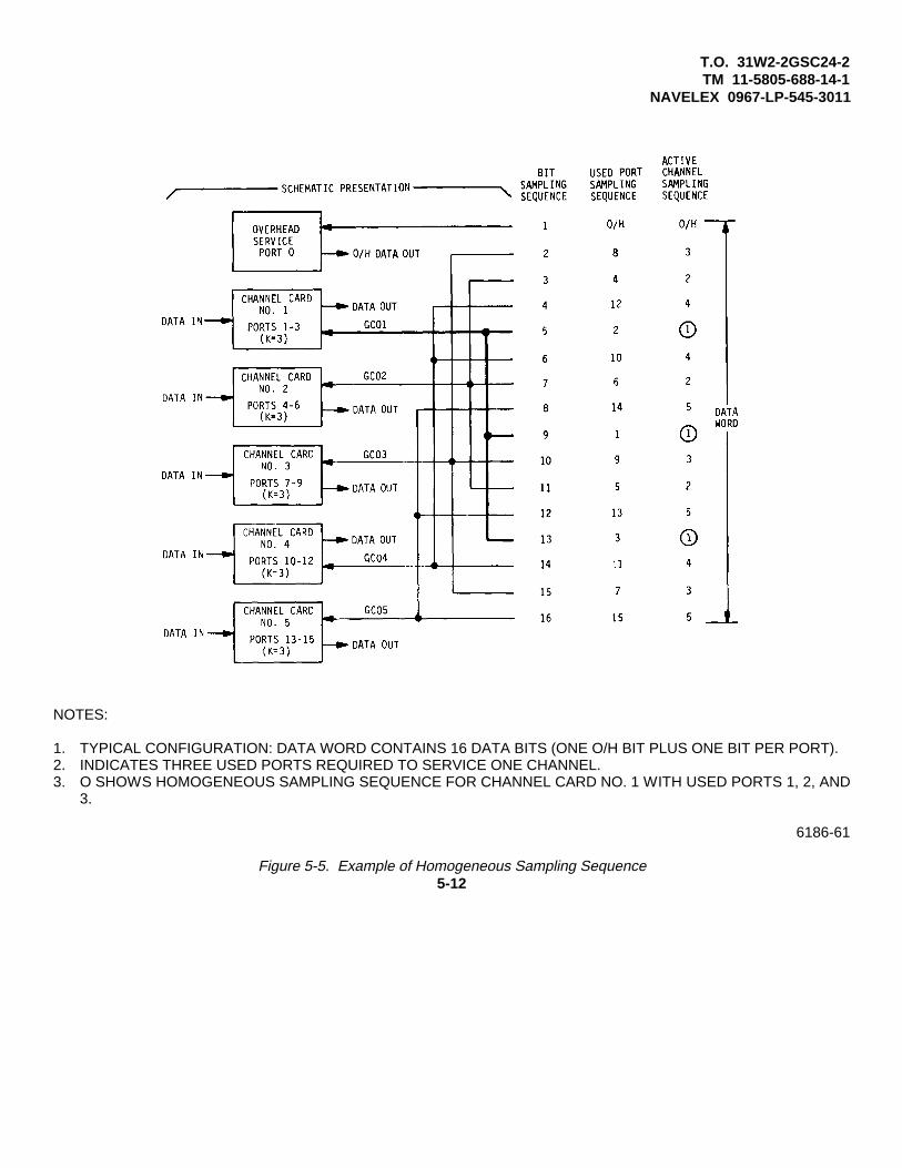
T.O. 31W2-2GSC24-2TM 11-5805-688-14-1
NAVELEX 0967-LP-545-3011
NOTES:
1. TYPICAL CONFIGURATION: DATA WORD CONTAINS 16 DATA BITS (ONE O/H BIT PLUS ONE BIT PER PORT).2. INDICATES THREE USED PORTS REQUIRED TO SERVICE ONE CHANNEL.3. O SHOWS HOMOGENEOUS SAMPLING SEQUENCE FOR CHANNEL CARD NO. 1 WITH USED PORTS 1, 2, AND
3.
6186-61
Figure 5-5. Example of Homogeneous Sampling Sequence5-12

T.O. 31W2-2GSC24-2TM 11-5805-688-14-1
NAVELEX 0967-LP-545-3011
NOTES:
1. THESE 16 BITS REPRESENT ONE WORD IN A MULTIPLEXER CONFIGURATION SERVING 15 USED PORTS (1OVERHEAD PORT + 15 USED PORTS).
2. WAVEFORMS (B) AND (C) REPRESENT CHANNEL NO. 1 CONFIGURED FOR THREE USED PORTS. 3. WAVEFORMS (D) AND (E) (REPRESENT OVERHEAD FUNCTION PERFORMED ON CHANNEL NO. 1 DURING
WORD 29 .
6189-60AFigure 5-6. Gated Clocks - Waveform Diagram
Change 1 5-13

T.O. 31W2-2GSC24-2TM 11-5805-688-14-1
NAVELEX 0967-LP-545-3011
Reversed Resultant Used AssociatedDecimal Binary Binary Decimal Port ChannelCount Count Count Count Sequence Sequence
1 00001 10000 16 Bypass2 00010 01000 8 8 33 00011 11000 24 Bypass4 00100 00100 4 4 25 00101 10100 20 Bypass6 00110 01100 12 12 4
weighting to achieve near-homogeneous gatingsimplifies the logic implementation required for extractingdata from the channel cards. This is further described inthe theory of operation for the sequencer card(paragraph 5-265).
5-48. OVERHEAD SERVICE FUNCTION.
5-49. It is possible that the applied channel data ratecould vary with respect to the multiplexer timing ratesince the incoming data are asynchronous to themultiplexer set. As described in paragraphs 5-30through 5-35, the multiplexer channel cards can detectdifferences in the input and output rates and causecorrective action when the differences are less than +250ppm. The differences between the input and output databit rates are compensated by the use of an overheadservice function. Using overhead servicing, the multiplexfunction has the ability to add or delete gated clocksignals sent to the channel card as necessary tomaintain bit count integrity.
5-50. Figure 5-7 is a simplified block diagram of theprinted circuit card assemblies involved in the overheadservice function. Basically, figure 5-7 is an expandedversion of figure 5-4 with greater emphasis on thecommon electronics functions. The overhead service’function is initially activated when a rate compare signalis applied to each channel card from the
OEG card. In turn, each channel card responds with oneof three requests back to the OEG card: no action,positive stuff, or negative stuff. In this discussion,assume that channel card No. 1 requests no action,channel card No. 2 requests a positive stuff, andchannel card No. 3 requests a negative stuff
5-51. A no-action request from channel card No. 1indicates that the rate at which data are being written intothe channel card is the same as the rate at which dataare being read out. When the GC/DM gated clockgenerator card transmits channel No. 1 address to theOEG card, the no-action request signal is applied back tothe GC/DM card. As a result, the gated clock generatorcontinues to apply normal gated clock signals GCO1 tochannel card No. 1.
5-52. A positive stuff request from channel No. 2indicates that the rate at which data are being written intothe channel card is greater than the rate at which dataare being read out. When the gated clock generator onthe GC/DM card transmits channel No. 2 address to theOEG card, the positive stuff request signal is appliedback to the GC/DM card. As a result, one extra gatedclock signal GC02 is generated during word 29 in onepreselected minor frame. A channel card is eligible toreceive overhead service once in each major frameperiod during a specific
Change 5-14

T.O. 31W2-2GSC24-2TM 11-5805-688-14-1
NAVELEX 0967-LP-545-3011
6186-58Figure 5-7. Multiplexer Overhead Service - Simplified Block Diagram
minor frame for each used port assigned to the channel.For example, if channel No. 2 has three used ports, upto three extra gated clocks can be received during amajor frame period. Each extra gated clock occursduring one specific minor frame period.
5-53. A negative stuff request from channel No. 3indicates that the rate at which data are being written intothe channel card is less than the rate at which data arebeing read out. When the gated clock generator on theGC/DM card transmits channel No. 3
Change 1 5-15

T.O. 31W2-2GSC24-2TM 11-5805-688-14-1
NAVELEX 0967-LP-545-3011
address to the OEG card, the negative stuff requestsignal is applied back to the GC/DM card. As a result,one normal gated clock signal GC03 is deleted duringword 29 in one preselected minor frame.
5-54. Each additional gated clock signal generated asa result of a positive stuff request occurs during bit 0 in agiven word as shown in D of figure 5-6. Each gatedclock that is deleted as a result of a negative stuffrequest occurs in the first bit time assigned to the givenchannel as shown in E of figure 5-6. In a no-actioncondition, the channel continues to receive one gatedclock in each word period for each used port assigned tothe channel.
5-55. DEMULTIPLEXER BASIC CONCEPTS
5-56. Two functions are considered unique to theAN/GSC-24(V) demultiplexer. One is the framesynchronization function, which enables thedemultiplexer to acquire and maintain framesynchronization with the transmitting multiplexer. Suchsynchronization is accomplished in relatively severe errorenvironments. The second function is commonly termedsmoothing, and is associated with the demultiplexer’sability to compensate for stuffing operations performedby the multiplexer without inducing unacceptableperturbations in the demultiplexer channel timingoutputs. The frame synchronization and smoothingfunctions are conceptually introduced in paragraphs 5-57through 5-67.
5-57. FRAME SYNCHRONIZATION FUNCTION.
5-58. The demultiplexer uses a frame synchronizationtechnique that enables acquisition and maintenance offrame synchronization in the presence of errors in thereceived synchronization pattern. Such an arrangementensures a high degree of bit count integrity in situationswhere the multiplexer-to
demultiplexer transmission link may be subject to dataerrors induced by atmospheric fading, lightning hits, orother such phenomena.
5-59. Frame acquisition and maintenance by thedemultiplexer is accomplished by the use of the 23-bitstuff code pattern inserted in the overhead word of themultiplexer’s output (paragraph 5-13). As discussed inparagraph 5-13, each minor frame transmitted by themultiplexer contains one of three stuffing codes in thefirst 23 bit positions of the 29-bit overhead word. Thedemultiplexer is designed to recognize any of the threecodes and to synchronize its timing circuits with thereceived code. Within prescribed limits, received codesmay contain errors not present when the code wastransmitted by the multiplexer.
5-60. The demultiplexer frame synchronization circuitsoperate in two modes: frame acquisition and framemaintenance. When the demultiplexer first receives datafrom the transmitting multiplexer, the frame acquisitionmode is automatically selected. Once initial frameacquisition is accomplished within prescribed errorlimitations, the frame synchronization circuits switch to aframe maintenance mode. The circuits remain in thismode until the number of received errors exceeds asecond set of prescribed limits or until the demultiplexerdata input is otherwise interrupted. Figure 5-8 depicts asimplified block diagram of the demultiplexer framesynchronization function.
5-61. In the frame acquisition mode, serial dataentering the demultiplexer are routed to a variable lengthshift register (VLSR) whose length is controlled by portstrapping assignments in the demultiplexer commonelectronics section. The varying of shift register length isset to correspond to the variable length data wordtransmitted by
Change 1 5-16

T.O. 31W2-2GSC24-2TM 11-5805-688-14-1
NAVELEX 0967-LP-545-3011
6186-85Figure 5-8. Frame Synchronization Function - Simplified Block Diagram
the multiplexer (paragraph 5-11). An 11-bit stuff codecomparator performs a broadside or parallel search foran exact match between the data flowing through theVLSR and one of three stuff codes contained in thecomparator. When one of the three codes is detectedwithout errors, the stuff code comparator sets a parallelsync latch. This latch, in turn, presets the demultiplexerword counter and an up/ down confidence counter, andenables a serial error detector. The word counter ispreset to 12, since the next received multiplexer word is12. The confidence counter is set to a count of 5. Onceparallel sync is established without detected errors in thefirst 11 bits of the received framing code, the next 12 bits(11 + 12 = 23 total stuff code bits) of received overheaddata are compared serially by the serial error detector.To enable comparison,
the stuff code store provides the remaining 12 bits of theappropriate one of the three known code possibilitiesunder control of the word counter. Each error detectedduring the serial comparison is counted by an errorcounter whose output is routed to the up/downconfidence counter. If the number of errors detectedduring the serial code comparison is two or less, theframe sync latch is set and the frame synchronizationcircuits automatically switch to a frame maintenancemode. If more than two errors are detected, the wordcounter and parallel sync latch are reset and the frameacquisition cycle is initiated again.
5-62. Frame maintenance is accomplished by a serial23-bit comparison of the received overhead stuffingcodes and known codes provided by the stuff.
5-17

T.O. 31W2-2GSC24-2TM 11-5805-688-14-1
NAVELEX 0967-LP-545-3011
code store. In the frame maintenance mode, each 23-bitpattern containing seven or less errors causes the up/down confidence counter to be incremented by onecount, and the frame sync latch to remain set. Eachreceived code containing more than seven errors causesthe up/down confidence counter to be decremented byone count. If several successive codes containing morethan seven errors are detected, the confidence counter isdecremented to 0 and the frame sync latch is reset to aloss-of-frame condition. In such an event, the frameacquisition mode is again automatically initiated.
5-63. Based upon the above discussion, it can beestablished that the demultiplexer frame synchronizationfunction operates in two automatically selected modes:acquisition and maintenance. Frame acquisition isaccomplished by a combined parallel and serial searchfor one of the three overhead stuffing codes transmittedby the multiplexer. Frame maintenance is achieved by a23 bit serial search for one of the three possible codes.In either the acquisition or maintenance mode, aprescribed number of detected code errors may bepresent without causing disruption of the overall framesynchronization process. Further discussion of theframe synchronization function is presented inparagraphs 5-108 and 5-472.
5-64. SMOOTHING FUNCTION.
5-65. When outputting data other than voice, channelcards in the demultiplexer perform a synchronous-to-asynchronous buffering process that is the inverse of thestuffing operation performed in the multiplexer. Thedemultiplexer destuffing process results in reinsertion ofthose rate variations that were present at the transmittingmultiplexer’s channel inputs.
5-66. A smoothing function is also accomplished by ananalog phase-locked
loop arrangement as depicted in simplified form in figure5-9. Under control of a gated clock (GC) signalgenerated within the demultiplexer common electronicssection, data bits associated with a given channel areread from the serial data bus into the channel cardelastic storage register. The GC signal exactly matchesthe GC signal applied to the transmitting multiplexerchannel card, and therefore may have individual clocksadded or deleted as necessary to accommodate channelrate variations applied to the multiplexer’s channel input.Data in the demultiplexer channel card’s elastic storageregister are read out under control of a clock provided bya voltage-controlled multivibrator (VCM). Located on thechannel card, the VCM is configured to operateindependent of the GC at the channel’s nominal outputdata rate, and also provides the channel’s output timingsignal.
5-67. Since there are variations in the rate of the GCtiming signal, the VCM and GC signals are phase lockedto prevent underflow or overflow of the elastic storageregister. A phase comparator determines when apredetermined offset between the channel card’s inputand output counters increases or decreases beyondacceptable limits. When an unacceptable offset isdetected, the phase comparator yields a correspondingerror signal that is routed, via a filter/amplifier network, tothe frequency control input of the VCM. Thus, when theinput counter is determined to be operating faster thanthe output counter, the resultant error signal causes anincrease in the VCM output frequency. In turn, when theinput counter is determined to be operating slower thanthe output counter, the resultant error signal causes adecrease in the VCM output frequency. The net effect isthat the input counter and output counter timing sourcesare phase locked. Circuits within the filter/amplifiernetwork are
Change 1 5-18

T.O. 31W2-2GSC24-2TM 11-5805-688-14-1
NAVELEX 0967-LP-545-3011
6186-86Figure 5-9. Smoothing Function - Simplified Block Diagram
designed to integrate the error signal output of the phasecomparator. Therefore, a detected input/output counteroffset is corrected over numerous periods of the VCMoutput rather than instantaneously. The correctionprocess over an extended time interval assures a
smooth variation in the channel’s output timing signaland provides the basis for the term smoothing. A moredetailed discussion of the smoothing function ispresented in paragraph
5-19

T.O. 31W2-2GSC24-2TM 11-5805-688-14-1
NAVELEX 0967-LP-545-3011
SECTION II
MULTIPLEXER, DEMULTIPLEXER, AND OVERALL DIAGNOSTICSFUNCTIONAL BLOCK DIAGRAM DISCUSSIONS
5-68. This section contains separate functional blockdiagram discussions for the multiplexer, demultiplexer,and overall diagnostics. The overall diagnosticsfunctional block diagram discussion includes thediagnostic circuits associated with the multiplexer,demultiplexer, and power supply. The block diagramdiscussions of the circuits on the front panel are alsoincorporated into the overall diagnostics circuitdiscussion.
5-69. OVERALL MULTIPLEXER FUNCTIONALBLOCK DIAGRAM DISCUSSION.
5-70. GENERAL. A multiplexer configuration usesbetween 1 and 15 channel option cards to receive up to15 channels of asynchronous digital data and/ or voicedata from associated communications links. The threetypes of channel cards that can be used to receive datain a multiplexer configuration are shown in figure FO-1.The block diagram also shows the four common cards ina multiplexer configuration that generate the timing andcontrol signals that perform the time-division multiplexand overhead service functions for the incoming channeldata.
5-71. RATE COMPARISON BUFFER (RCB) CARD.
5-72. The RCB card receives asynchronous data thatare clocked into a temporary storage register by its ownassociated timing signals. At a later time, data areclocked out of the storage register and are routed to theGC/DM card by signals that are synchronous with themultiplexer timing function. The write and read functions
for the storage register are independent of each other;the only restriction is that data written into a givenaddress cannot be simultaneously read out of theaddress.
5-73. As shown in figure FO-1, digital data signalsDIXX are applied to a data receiver on the RCB card.The data receiver conditions the data into TTL levelscompatible with the logic circuits in the multiplexer. Theassociated timing signals are applied to a timing receiverthat conditions the signals into TTL levels. Theconditioned timing signals are routed to increment thewrite address counter. The write address counter, in turn,generates sequential write addresses that clock theconditioned data into the data elastic storage register.The read address counter is sequentially incremented bygated clock signals (MGCO1) that are applied at a portrate (Rp) nominally the same as the incoming data rate.The read address counter is offset from the writeaddress counter so that the read address selected at anygiven time is always delayed from the write address.The data are therefore not simultaneously read in andout of the register for a given address. The data read outof the register are applied to the data output buffer. Thedata are clocked through the buffer to the GC/DM cardby multiplexer clock signal MRI01-.
5-74. The rate compare and stuff request circuits onthe RCB card are part of the multiplexer overheadservice function to compensate for changes in theincoming bit rate. The rate compare circuits detect anyvariation between the incoming bit rate and the
5-20
T.O. 31W2-2GSC24-2TM 11-5805-688-14-1
NAVELEX 0967-LP-545-3011
precision multiplexer channel sampling rate (KRp)applied to the channel. During word 24, the ratecomparison function is initiated by word 24 bit 0 signalMW2401 from the OEG card. At this time, the ratecompare circuits effectively subtract the count in thewrite address from the count in the read address. Innormal operation, there is a predetermined differencecount between the two addresses. When the differencecount from a rate compare is the predetermined figure, ano action request is generated. When the incoming bitrate increases, the difference count indicates that thewrite address is greater than the read address. At thistime, a positive stuff request is generated and applied tothe OEG card. As a result, an additional gated clockpulse applied to the RCB card effectively helps the readaddress counter to catch up. When the difference countindicates that the incoming bit rate has decreased, thewrite address is less than the read address and anegative stuff request is generated. The result is that onenormal gated clock pulse to the RCB card is deleted,which effectively slows down the channel sampling rateof the read address counter. The stuffing action foreither the positive or negative stuff condition continuesas long as the rate compare circuits determine that theincoming bit rate and the channel sampling rate are notnominally the same. Each used port assigned to a givenchannel is eligible to receive overhead servicing duringone minor frame in each minor frame period.
5-75. Initially, when an RCB card is configured for adata channel and the applied data rate to the card is thesame (within +250 ppm) as the channel sampling rateapplied to the card, the RCB/URC switch on the card isset to the RCB position. With the switch in the RCBposition, the circuits on the card function as describedabove. When the channel sampling rate for a channelnot be configured to be within +250
ppm of the incoming data rate, a channel sampling ratethat is higher than the incoming data rate is selected. Inthis configuration, the RCB/URC switch on the card is setto the URC position to place the coarse rate conversioncircuits in series with the applied gated clocks. Thecoarse rate conversion circuits are configured to delete apredetermined number of gated clock signals andeffectively lower the channel sampling rate to within +250ppm of the incoming data rate. The word 24 signalMW24N1, end-of-scan signal MEOS3NX, and minorframe terminal count signal MMFC31 are timing signalsthat control the selection of the individual gated clockpulses that are deleted, inhibit the coarse rate conversioncircuits during word 29 when overhead servicing isperformed, and preset the circuits after each majorframe period. The coarse rate conversion circuits areindependent of the positive and negative stuff functionperformed in the rate conversion buffer circuits asdescribed in paragraph 5-74. Fixed amounts of gatedclock pulses are deleted by the coarse rate conversioncircuits during each major frame period.
5-76. TRANSITION ENCODER/TIMING RECOVERY(TE/TR) CARD.
5-77 The TE/TR card processes digital data that areapplied to the multiplexer without timing. The circuits onthe card are divided into three functional circuits: thetransition encoder circuits that receive and processdigital data whose bit rate is 400 bps or less; the timingrecovery circuits that receive and process digital datawhose bit rate is 75, 100, 150, 300, 600, 1200, 4800, or9600 bps; and the rate comparison buffer (RCB) circuitsthat receive the data from the transition encoder or thetiming recovery circuits and resynchronize the data bitswith the multiplexer timing as described in the RCB carddiscussion.
Change 1 5-21

T.O. 31W2-2GSC24-2TM 11-5805-688-14-1
NAVELEX 0967-LP-545-3011
5-78. The timing recovery (TR) circuits generate thetiming signals that are synchronized with the incomingasynchronous digital data. As described in the RCB carddiscussion, the timing signals are necessary to clock theincoming data pulses into the RCB circuits. The datareceiver in the timing recovery circuits conditions theapplied digital data (DIXX) into TTL levels that arecompatible with the logic circuits on the card. The datapulses are applied to a transition detector circuit and tothe RCB circuits. The transition detector circuit applies areset signal to the timing generator circuit each time apulse transition occurs. The timing generator circuit, inturn, receives a continuous timing output from the timingoscillator. The timing signals are divided down toproduce the selected timing output rate that is the sameas the incoming data bit rate. By resetting the timinggenerator circuits each time a positive-going or negative-going pulse transition occurs, the continuous TR timingsignals to the RCB circuits are effectively held insynchronization with the conditioned data pulses appliedto the RCB circuits.
5-79. The transition encoder circuits generate thetiming signals that are synchronized with the incomingasynchronous digital data. The data receiver in thetransition encoder circuits conditions the applied digitaldata and applies the conditioned pulses to the 3-bittransition encoder circuits. Each time a positive-going ornegative-going transition of a data pulse occurs, the 3-bittransition encoder circuits generate a 3-bit digital codethat is synchronous with the TE timing pulses beingapplied to the RCB circuits. The 3-bit code identifies thefollowing: that a transition has occurred; the position ofthe transition as related to the first half or the second halfof the timing signal at the time of transition; and that the
pulse transition is a positive-going or a negative-goingtransition. The timing signals from the timing generatorto the RCB circuits are developed from the T4800 or theT3600 (Hz) timing signals from the RT card. Theselected timing rate is either 225, 300, 450, 600, 900, or1200 Hz, corresponding to the input rate ranges of 75,100, 150, 200, 300 or 400 bps, respectively. The timingsignals also synchronize the 3bit code output from theencoder so that the 3-bit data codes and the TE timingsignals applied to the RCB circuits are synchronous
5-80. The TE/TR switches on the card are set to applythe data and associated timing signals from the TE or TRcircuits to the RCB circuits. The RCB circuits processthe incoming data to be synchronous with the multiplexertiming functions as described for the RCB card. TheRCB circuits on the TE/ TR card do not have the coarserate conversion circuits associated with the RCB card.The data output (MDT002) is clocked to the GC/DM cardby system clock signal MRI02-. The positive andnegative stuff request signals (MPST02 and MNST02)are applied to the OEG card.
5-81. VOICE ENCODER (VE) CARD.
5-82. The VE card receives one voice channel andconverts the incoming analog signals into synchronousdigital data that can be combined with other datachannels in the GC/DM card. The VE card processessignals in the range of 150 to 3500 Hz. The voicesignals are applied to a voltage comparator circuit thatcompares the incoming analog signals with areconstructed analog signal voltage from the D/Aconversion circuits. In real time, the reconstructedanalog signals should be almost identical to the incominganalog signals to the card. The difference voltagedeveloped in the voltage comparator circuit is applied asan error voltage to the digital sample and control circuits.
5-22

T.O. 31W-2GSC24-2TM 11-5805-688-14-1
NAVELEX 0967-LP-545-3011
5-83. In normal operation, an analog error voltage,which continually varies in amplitude and polarity, isgenerated from the voltage comparator. The errorvoltage is translated into digital data in the digital sampleand control circuits. The digital data from the digitalsample and control circuits are applied to the data outputbuffer and to the D/A conversion circuits. The data fromthe data output buffer are clocked to the GC/DM card bymultiplexer clock signal MRI02-.
5-84. The digital data applied to the D/A conversioncircuits are converted from digital to analog voltages thatare representative of the incoming voice signals. Thereconstructed signal voltages from the D/A conversioncircuits are identical to the voltage waveforms that willbe decoded in the far-end demultiplexer. A slope controlsignal from the digital sample and control circuitseffectively speeds up the D/A conversion circuits to trackand convert the higher frequency and/or higheramplitude segments of the voice signals with a minimumamount of distortion.
5-85. SEQUENCER (SEQ) CARD.
5-86. The seq card generates the channel address,end-of-scan, and overhead MMF=PS signals that areapplied to the GC/DM card for timing purposes. ThePORT STRAPPING switches on the card are manuallyset to select up to 15 active channels and up to 31 usedports. The PORTS IN USE switches on the card are setto indicate the maximum number of used ports in a givensystem configuration. End-of-scan timing signals aregenerated on the card and applied to the GC/DM cardand the OEG card.
5-87. The channel address generation circuits on theseq card generate 4-bit binary channel address signalsMCHAD1 through MCHAD8. These signals, which aregenerated at the system clock rate (MRIO), are routed tothe GC/DM card. Each 4-bit channel address applied to
the GC/DM card causes one gated clock signal to begenerated to the channel card contained in the channeladdress.
5-88. The end-of-scan generator circuits generateend-of-scan signal MEOS, which is applied to the OEGcard when the port count in the sequencer timing circuitsis equal to the maximum number of used ports selectedby the PORTS IN USE switches. End-of-scan signalsMEOS2B and MEOS2B- are derived from signal MEOSand applied to the GC/DM card. The end-of-scan signalseffectively represent one word period.
5-89. The overhead port sequence selector circuitproduces minor frame equals port sequence signalMMF=PS, which is applied to the GC/DM card. Thesignal is generated during each minor frame period thatis eligible to provide overhead service to an as-signed used port.
5-90. OVERHEAD ENABLE GENERATOR (OEG)CARD.
5-91. The OEG card generates negative and positivestuff request signals, as well as timing signals used byother cards in the multiplexer. Negative and positivestuff request signals MPSTOX and MNSTOX are appliedto the OEG card from the active channels that use theRCB card or the TE/TR channel card. Each channelcard input to the OEG card is interrogated for a stuffrequest as selected by the overhead address countsignals MOHO through MOH3. The overhead countaddress signals are applied to the address select inputson the stuff request multiplexers. When the selectedchannel has a positive or negative stuff request, apositive stuff request signal MPSA- or a negative stuffrequest signal MNSA- is applied back to the GC/DMcard.
Change 1 5-23

T.O. 31W-2GSC24-2TM 11-5805-688-14-1
NAVELEX 0967-LP-545-3011
5-92. The word 24 generation circuits generate word24 bit 0 signal MW240X and word 24 signal MW24NXwhen the word count in signals WCO through WC4 fromthe GC/DM card contains a count of 24 and multiplexerclock signal MRIO occurs. The word 24 signals areapplied to the channel cards to initiate the overheadservice function as described in the RCB carddiscussion. The end-of-scan generation circuits produceend-of-scan signal EOS2 to the word 24 generationcircuits when end of-scan signal MEOS is applied fromthe seq card. At the same time, the circuits alsogenerate end-of-scan signal MEOS3NX that is applied tothe RCB cards in the multiplexer.
5-93. The system clock distribution circuits receivesystem clock signal from the RT card and, in turn,generate the multiplexer clock signals MRIO1- throughMRI08-. These signals are distributed to the channelcards as timing signals. System clock signal MRIO thatis applied to the GC/DM card is identical to system clocksignals MRIO1- through MRI08-.
5-94. GATED CLOCK/DATA MUX (GC/DM) CARD.
5-95. The GC/DM card receives and combines thechannel data from the active channel cards into oneserial data stream that is applied to the RT card. Controland timing signals used in the multiplexer function arealso generated on the card as described below.
5-96. The word generation circuits generate wordcount signals WCO through WC4 to provide 5-bitsequential word counts 1 through 29. The signals areapplied to the stuff code generation circuits. Word countsignals WCO, WC1, and WC2 are applied to theoverhead data multiplexer, and word count signalsWCO, WC1, WC2, and WC4 are applied to the OEGcard. The circuits also
generate word 27 signal W27, word 28 signal MW28,and words 24 through 29 signal MWC2429 that are usedfor timing purposes on the card. Word 28 signal MW28is routed to the seq card as a control signal.
5-97. The stuff code generation circuits generate threedifferent 23-bit stuff command codes: the positive stuffcode (PSC), the negative stuff code (NSC), and the noaction code (NAC). All three codes are generated at thesame time, during word counts 1 through 23, and areapplied to the overhead data multiplexer.
5-98. The minor frame generation circuits produceminor frame count signals MMFCO through MMFC4 thatsequentially count minor frames 1 through 31. Thesesignals are applied to the overhead data multiplexer andto the seq card. During minor frame count 31, minorframe terminal count signal MMFC31 is generated andapplied to the channel cards that use the RCB card.Signal MMFC31 represents one major frame period.The minor frame count is advanced one count each timeend-of-scan signal MEOS2B- from the seq card andword 29 signal W29 from the word generation circuitsoccur.
5-99. The gated clock generation circuits generategated clock signals (MGCO1 through MGC15) asrequired to service the active channel cards. One gatedclock signal is generated for each active channel. Forexample, a multiplexer with 10 active channels usesgated clock signals MGCO1 (channel 1) through MGC10(channel 10). Each gated clock signal applied to anactive channel gates one channel data bit to the outputdata multiplexer on the card. At the same time that agated clock signal is generated, 4-bit binary channeladdress signals GCAD1 through GCAD8, which containthe same address as the active channel being
Change 1 5-24

T.O. 31W-2GSC24-2TM 11-5805-688-14-1
NAVELEX 0967-LP-545-3011
serviced, are generated and applied to the select inputson the output data multiplexer. Each used port in anactive channel in the multiplexer receives one gatedclock signal that gates one data bit to the GC/DM cardduring each word time; the exception is during word 29when overhead servicing is performed. When positivestuff enable signal MPSE is applied to the circuits duringword 29, one additional gated clock signal is generatedto the active channel selected for overhead servicing. Inturn, when negative stuff enable signal MNSE is applied,one gated clock signal, which is normally applied to theselected active channel, is deleted as part of theoverhead service function.
5-100. The overhead data multiplexer combines theoverhead data inputs for a given port selected foroverhead servicing into a serial format. The serialoverhead data are clocked into the output datamultiplexer during bit 0 of each data word period. Words24 through 29 signal MWC2429-enables minor framecount signals MMFCO through MMFC4 to be applied,one bit at a time, to the overhead data multiplexer.Word count signals WCO, WC1, and WC2 sequentiallyclock the five minor word count signals into the outputdata multiplexer. The appropriate 23-bit stuff codeclocked into the overhead data multiplexer during words1 through 23 is selected by positive stuff request signalMPSA or negative stuff request signal MNSA from theOEG card. The absence of both signals from the OEGcard enables the no-action code. When signal MPSA isapplied to the multiplexer, positive stuff enable signalMPSE is generated and applied to the gated clockgeneration circuits. When signal MNSA is applied to themultiplexer, a negative stuff enable signal is generatedand applied to the gated clock generation circuits. Theoutput from the overhead data multiplexer is the serial29-bit overhead message that is applied to the outputdata multiplexer during bit 0 of words 1 through 29.
5-101. The output data multiplexer interleaves, one bitat a time, the data inputs from each of the activechannels and the overhead data input from theoverhead data multiplexer. The high-speed serial datastream (MSD) from the multiplexer is applied to the RTcard. The 4-bit binary channel address signals GCAD1through GCAD8 select the appropriate overhead or datachannel input to the multiplexer at the system clock rateMRIO. The channel address applied to the multiplexeris the same channel address in the gated clock signalthat is generated at any given time. For example,channel 2 is receiving a gated clock signal MGC02 atthe same time that the channel address signal forchannel 1 is applied to the multiplexer. The high-speedserial data stream is clocked out of the multiplexer bysystem clock signal MRIO.
5-102. REFERENCE TIMER (RT) CARD.
5-103. The RT card produces system clock signal Ro
and timing signals T3600 and T4800 used in themultiplexer cards. The high-speed serial data stream(MSD) from the GC/DM card is conditioned in the RTcard and is then applied, with associated timing signals,to the rear panel, where the signals are fed into abalanced or unbalanced cable system.
5-104. The high-speed serial digital data stream fromthe GC/DM card is clocked into the output data linedriver by system timing signal Ro. The digital data areconditioned into digital signals that can be applied to abalanced line or an unbalanced line input. In a balancedline configuration, the output data signals aretransmitted as complementary serial data out signalsSDATO and SDATO-. In the unbalanced lineconfiguration, signal SDATO-is terminated (grounded).System
5-25

T.O. 31W-2GSC24-2TM 11-5805-688-14-1
NAVELEX 0967-LP-545-3011
timing signal Ro and multiplexer timing out signalsTIMOUT and TIMOUT- are generated by the outputtiming line driver. These timing signals are derived froman external timing reference source that is appliedthrough the EXT position of the EXT/INT switch, or froma precision master oscillator on the RT card through theINT position of the EXT/INT switch. In a balanced lineconfiguration, the timing signals are transmitted ascomplementary signals TIMOUT and TIMOUT-. In theunbalanced configuration, signal TIMOUT- is terminated(grounded). The output timing line driver also generatessystem clock signal Ro that is identical to the TIMOUTsignal. Signal is applied to the OEG card.
5-105. The timing recovery (TR) timing generationcircuits produce precision 3600-Hz and 4800-Hz timingsignals that are applied as timing signals T3600 andT4800 to the TE/TR cards in the multiplexer.
5-106. OVERALL DEMULTIPLEXER FUNCTIONALBLOCK DIAGRAM DISCUSSION.
5-107. GENERAL. A demultiplexer configuration usesbetween one and 15 channel option cards to process upto 15 channels of asynchronous digital data (with orwithout timing) and/or voice data outputs to associatedcommunications links. The four types of output channelcards that can be used in the demultiplexer are the SB,NBSB, TD, and VD cards. Five common cards used inthe demultiplexer generate the timing and controlsignals for demultiplexing the applied high-speed serialdata stream from the far-end multiplexer. The OEG,GC/DM, seq, FS, and ERD cards are the common cardsin the demultiplexer. The overall demultiplexer blockdiagram is shown in figure FO-2.
5-108. FRAME SYNC (FS) CARD.
5-109. The FS card buffers the incoming high-speeddigital data and distributes the incoming data to all thechannel cards in the demultiplexer. A framesynchronization function and an overhead decodefunction are also performed on the FS card. The framesynchronization function synchronizes the demultiplexertiming generation circuits to the timing associated withthe incoming data. The overhead decode functiondecodes one of the three stuff codes that are in theoverhead message during each minor frame period.
5-110. The incoming high-speed digital data stream(DATA) is applied to the data receiver circuits where thedata are conditioned into the TTL levels that arecompatible with the logic circuits in the demultiplexer.The data for the data receiver are applied to thechannel data output shift register, parallel syncacquisition circuits, and serial sync and syncmaintenance circuits. The data are clocked through thechannel data output shift register by system input clocksignals RIO from the timing receiver circuits. The shiftregister output is inhibited by the absence of frame syncsignal DFS from the serial sync and sync, maintenancecircuits when frame synchronization is lost. In normaloperation, demultiplexer input data signals (DTIX-)clocked through the shift register are routed to eachchannel card in the demultiplexer,
5-111. The parallel sync acquisition circuits establishthe initial synchronization of the demultiplexer timingwith she incoming data timing. The circuits search theapplied data for the first 11 bits of the overheadmessage located in bit 0 of the first 11 words. Since thefirst 23 bits of the
5-26

T.O. 31W-2GSC24-2TM 11-5805-688-14-1
NAVELEX 0967-LP-545-3011
overhead message contain one of the three fixed stuffcommand codes, the first 11 bits are predictable andcan be identified. When the first 11 bits of one of thethree stuff command codes is identified, demultiplexerframe sync signal DSYNC- is generated and applied asan enable signal to the serial sync and syncmaintenance circuits. Signal DSYNC- is also applied tothe seq card to synchronize the channel addressgeneration circuits with the incoming data timing. Theserial sync and sync maintenance circuits then monitoroverhead bits 12 through 23 in the overhead messageduring the same minor frame in which bits 1 through 11were identified. When overhead bits 12 through 23 aresuccessfully identified as part of a given stuff commandcode, frame synchronization is effectively completed. Atthe time that signal DSYNC is applied, the serial syncand sync maintenance circuits produce demultiplexerword counter preset signal DWPR that is applied to theGC/DM card to synchronize the gated clock generationcircuits with the incoming data timing.
5-112. Once frame synchronization is established,demultiplexer frame sync signal DFS is generated andapplied as an enable signal to the channel data outputshift register and to the error rate detector circuits on theERD card. Signal DFS is also applied to the parallelsync acquisition circuits as an inhibit signal that preventsthe circuits from being enabled again until framesynchronization is lost. After initial framesynchronization, the serial sync and sync maintenancecircuits continue to check that one of the three stuffcode patterns generated (during words 1 through 23) bythe stuff code generation circuits on the GC/DM card isthe same as the stuff code pattern contained in theincoming data overhead message format. When theincoming pattern does not match one of the threepatterns from the GC/DM card, an out-of-synchronization state is identified and signal DFS is
removed. This causes the channel data output shiftregister on the FS card and the error rate detectorcircuits on the ERD card to be inhibited. At the sametime, removal of signal DFS also enables the parallelsync acquisition circuits to start another initial framesynchronization search. Assuming that the equipmentand incoming signals are not in a permanent errorcondition, signal DFS will again be generated andmaintained as long as a synchronous timing condition ispresent. The serial sync and sync maintenance circuitsalso generate demultiplexer overhead data signals DOD-(bit 0 of each word) that are applied to the ERD card.As part of the sync maintenance function, the incomingstuff command code is decoded, and negative stuffenable signal DNSE or positive stuff enable signalDPSE is produced. The absence of both signals duringa minor frame period indicates the presence of the no-action condition. These signals are applied to theGC/DM and ERD cards to initiate the appropriatestuffing action. Word 29 signal DW29 and end-of-scansignals DEOS2 and DEOS2- are applied as part of thedemultiplexer timing function.
5-113. SEQUENCER (SEQ) CARD.
5-114. The seq card generates the channel address,end-of-scan, and overhead DMF=PS signals that areapplied to the GC/DM card for timing purposes. ThePORT STRAPPING and PORTS IN USE switches onthe card are set to the same switching configuration asthat used on the seq card in the far-end multiplexer.End-of-scan timing signals generated on the seq cardare also applied to the ERD and OEG cards.
5-115. The channel address generation circuits on theseq card generate 4-bit binary channel address signalsDCHAD1 through DCHAD8. These signals, which aregenerated at the system clock rate
5-27

T.O. 31W-2GSC24-2TM 11-5805-688-14-1
NAVELEX 0967-LP-545-3011
(DRIO), are routed to the GC/DM card. Each 4-bitchannel address applied to the GC/DM card causes onegated clock signal to be generated to the channel cardidentified in the channel address. The end-of-scangeneration circuits generate complementary end-of-scansignals DEOS and DEOS- that are applied to the OEGand ERD cards. The signals are generated when theport count in the sequencer timing circuits is equal tothe maximum number of used ports selected by the fivePORTS IN USE switches. Complementary end-of-scansignals DEOS2 and DEOS2- are derived from signalDEOS and the signals are applied to the FS card. Inturn, complementary end-of-scan signals DEOS2B andDEOS2B- are also derived from signal DEOS. Thesetwo signals are routed to the OEG, GC/DM, and ERDcards. The overhead port sequence selector circuitproduces minor frame equals port sequence signalDMF=PS during each minor frame period that is eligibleto provide overhead service to an assigned used port.The signal is applied as an enable signal to the GC/DMcard during word 29 to allow a positive or negative stuffto be performed. The five minor frame count signals,DMFCO through DMFC4, that are applied to the circuitfrom the ERD card contain the minor frame number of agiven minor frame being received in the demultiplexer atany given time.
5-116. OVERHEAD ENABLE GENERATOR (OEG)CARD.
5-117. The OEG card generates timing signals that areused in the demultiplexer function. The word 24generation circuits generate word 24 signal DW24NXwhen the word count in word count signals DWCOthrough DWC4 from the GC/DM card is count 23, andend-of-scan signal EOS is applied from the end-of-scangeneration circuits. Signal DW24NX is routed to theCRC circuits on the SB card(s) as a timing signal.
5-118. The system clock distribution circuits generatesystem clock signals DRIO from system clock signal RIfrom the FS card. Signals DRIO are routed as timingsignals to the seq and GC/DM cards. The end-of-scan7eneration circuits produce end-of-scan signalDEOS3NX when word 29 signal DW29 from the GC/DMcard and end-of-scan signal DEOS from the seq cardare applied. Signal DEOS3NX is routed as a timingsignal to the CRC circuit on the SB card(s).
5-119. GATED CLOCK/DATA MUX (GC/DM) CARD.
5-120. The GC/DM card generates the gated clocksignals that are applied to the channel cards in thedemultiplexer. The card also generates the three stuffcommand codes and timing signals that are applied tothe common cards in the demultiplexer as described inthe following paragraphs. The gated clock generationcircuits produce gated clock signals (DGCO1 throughDGC15) as required to service the active channel cards.Each active channel card has a designated gated clocksignal. For example, channel card No. 1 receives signalGCO1 each time a gated clock is designated to thechannel card. Positive stuff enable signal DPSE appliedto the circuits during word 29 causes one additionalgated clock signal to be generated to a selected channelcard as part of the overhead service function. In turn,negative stuff enable signal DNSE results in deletion ofone gated clock signal during word 29 to the selectedchannel card. Minor frame equals port sequence signalDMF=PS applied to the circuits is an enable signal thatallows a positive or negative overhead service to beperformed during word 29 of a given minor frameperiod. Signal DMF=PS is not generated during minorframe periods that are not eligible to provide overheadservicing.
5-28

T.O. 31W-2GSC24-2TM 11-5805-688-14-1
NAVELEX 0967-LP-545-3011
5-121. The stuff code generation circuits produce thethree stuff command codes that are applied to the FScard as part of the frame synchronization function.End-of-scan signal DEOS2Bfrom the seq card is a timinginput to the circuits. During bit 0 of each word, one bitfrom each of the three stuff command codes is appliedto the FS card. When the demultiplexer has framesynchronization, one of the three bits applied to the FScard will compare with the equivalent bit in the incomingoverhead message format during words 1 through 23.
5-122. The word generation circuits produce word countsignals DWCO through DWC4 to provide 5-bitsequential word counts 1 through 29 to the OEG card.Word signals DW28 and DW29 are also produced bythe circuits. Word signals DW28 and DW29- are appliedas timing signals to the ERD card and the FS card.Word signal DW29 is applied to the OEG card.
5-123. ERROR RATE DETECTOR (ERD) CARD.
5-124. The ERD card generates a timing signal andmonitors the incoming serial data stream for errors toestablish confidence in the BCI of the incoming data.The minor frame generation circuits produce minorframe count signals DMFCO through DMFC4 that areapplied to the seq card. The minor frame identified inthe signals is the same minor frame that is identified inthe incoming overhead message format at any giventime. Timing signals DW28, DW29-, and DEOS- areused in the generation of the minor frame count signals.Demultiplexer overhead data signals DOD-, whichcontain the minor frame count for the minor frame in agiven overhead message during a minor frame period,are used to synchronize the minor frame generationcircuits.
5-125. The error rate detector circuits receive nine bit
error counts from the FS card: three that are associatedwith the positive stuff command codes; three that areassociated with the negative stuff command codes; andthree that are associated with the no-action commandcode. During word 28, only one set of error counts ismonitored by the circuits. The set of three error countsmonitored is selected by positive and negative stuffcommand code signals DNSE and DPSE from the FScard. When signal DNSE is applied, the error ratedetector circuits monitor the three bit error countsassociated with the negative stuff command codes. Thepositive stuff command codes are monitored whensignal DPSE is applied to the circuits. When bothsignals (DPSE and DNSE) are absent during a givenminor frame period, the three bit error countsassociated with the no-action command codes aremonitored. When the number of errors identified in theerror counts exceeds a predetermined threshold countwithin a given period of time, link error rate signal LLERis generated. Signal LLER causes the LINK ERRORRATE indicator on the front panel to light. When thenumber of errors detected within a given period of timedecreases to a value that is less than the predeterminedthreshold count, signal LLER is removed and theindicator goes out.
5-126. SMOOTHING BUFFER (SB) CARD.
5-127. The SB card receives the high speed serial datain the form of synchronous data (DTIX-) from the FScard. The SB card function is basically the complementof the RCB card function performed in the far-endmultiplexer. Each SB card demultiplexes one channel ofdata out of the high-speed serial data stream andconverts the data into the original asynchronous dataformat (with timing) that was applied to the far-endmultiplexer. This card also demultiplexes data originallyprocessed into the far-end multiplexer by
5-29

T.O. 31W-2GSC24-2TM 11-5805-688-14-1
NAVELEX 0967-LP-545-3011
a TE/TR card that was configured for the TE function.The original timing associated with the data processedby an RCB card is also reconstructed in the SB card.
5-128. The incoming data (DTIX-) are clocked throughthe data input buffer and are written into the data elasticstorage register. The data input buffer, write addresscounter, and data elastic storage register are clocked bygated clock signals DGCO1 from the GC/DM card. Thegated clock signals are applied directly to the buffer, thecounter, and the storage register when the SB/URDswitch is in the SB position. When the switch is in theURD position, the gated clock signals are effectivelyapplied through the coarse rate conversion (CRC)circuits to the buffer, the counter, and the storageregister. The function performed by the CRC circuits isthe same as that performed by the CRC circuits in theRCB card used in the multiplexer. The write addresscounter is sequentially incremented by each gated clockpulse applied to it. The rate at which the write addresscounter is incremented is, in effect, the nominal bit rateat which the data will be processed out of the channelcard. The write addresses from the write addresscounter enable the data bits to be written into the dataelastic storage register. The read addresses that clockthe data out of the data elastic storage register aregenerated by the read address counter. The readaddress counter, in turn, is incremented by the readclock pulses applied from the analog phase-locked loop(APLL) circuit.
5-129. The APLL circuit generates the read clockpulses that increment the read address counter. Theread address counter, in turn, produces the readaddress signals that read the data bits out of the dataelastic storage register. Tie APLL circuit contains aphase-locked loop configuration that
effectively causes the read address count from the readaddress counter to track the write address count fromthe write address counter on a bit-for-bit basis, whilemaintaining a difference count of eight between the twoaddresses. The APLL circuit also performs a smoothingfunction to compensate for any abrupt changes in thedata bit rate caused by the overhead stuffing function.The output clock signals from the APLL circuit areidentical to the read clock signals. The output clocksignals clock the data bits through the data output bufferto the data output drivers. The output clock signals alsoclock the timing output drivers to produce thecomplementary demultiplexer timing out signals TOXXand TOXX-. The data bits applied to the data outputdrivers are conditioned and processed intocomplementary demultiplexer channel data outputsignals DOXX and DOXX-.
5-130. NARROW BAND SMOOTHING BUFFER(NBSB) CARD.
5-131. The NBSB card is identical to the SB carddescribed in paragraphs 5-126 through 5-129. TheAPLL circuit on the NBSB card is physically different, butperforms the same functions as those described for theAPLL circuit on the SB card. The APLL circuit on theNBSB card is configured to provide a greater smoothingaction that occurs over a longer period of time asdescribed in the detailed theory of operation for theNBSB card. The NBSB card has a narrower range offrequencies that it can process as compared to the SBcard.
5-132. TRANSITION DECODER (TD) CARD.
5-133. The TD card receives the high-speed serial datain the form of synchronous data (DTIX-) from the FScard. The TD card function is basically the complementof the TE card function performed on the TE/TR card inthe multiplexer. Functionally, the TD carddemultiplexes one channel of data out
5-30

T.O. 31W-2GSC24-2TM 11-5805-688-14-1
NAVELEX 0967-LP-545-3011
of the high-speed serial data stream and converts thedata into the original asynchronous data format (withouttiming) that was applied to the far-end multiplexer.
5-134. The write and read function for writing andreading data bits into and out of the data elastic storageregister is the same as that described for the SB card.The data out of the register are arranged in a series of3bit transition codes. These codes are applied to thetransition decoder, which produces one pulse transitionfor each 3-bit code applied to it. The result is a series ofreconstructed data pulses that are clocked through thedata output buffer to the data output drivers. The pulsesapplied to the data output drivers are conditioned andprocessed into complementary demultiplexer channeldata output signals DOXX and DOXX-.
5-135. VOICE DECODER (VD) CARD.
5-136. The VD card receives the high-speed serial datain the form of synchronous data (DTIX-) from the FScard. The VD card function is basically the complementof the VE card function in the multiplexer. Functionally,the VD card demultiplexes one channel of digitized voicedata out of the high-speed serial data stream, convertsthese data into analog signals, and filters thereconstructed analog signals into the original voicewaveforms applied to the far-end multiplexer inputchannel.
5-137. The incoming digital data bits are appliedthrough a shift register to the digital-to-analog (D/A)conversion circuits. The analog signals from the D/Aconversion circuits are applied through a bandpass filtercircuit to the output amplifier-drivers. The signals areamplified through the output amplifier-drivers to producedata output signals DOXX and DOXX-
5-138. OVERALL DIAGNOSTIC FUNCTIONALBLOCK DIAGRAM.
5-139. GENERAL.
5-140. The diagnostic circuits in the multiplexer setmonitor the equipment for error conditions. When anerror is detected, a visual display on the front panelindicates the existence and source of the malfunction.On the front panel, the malfunction source is identified aseither a faulty input signal to the multiplexer set or as afailed subassembly within the equipment. The diagnosticcircuits also generate electrical error signals (remotealarms) representative of the front panel indications. Theremote alarm signals are routed to one multipinconnector on the rear panel, where the signals can beremoted to other equipment.
5-141. Each plug-in card type in the multiplexer setcontains diagnostic error detection circuits thatcontinually generate one or more error or no-error statussignals to the display card. The display card, in turn,generates signals that enable the indicators on the frontpanel when an error condition is detected. An errorstatus signal from the diagnostic circuit in the powersupply is routed directly to a diagnostic circuit on thefront panel. The remote alarm signals are generated bythe display card, the ERD card, and the front panel.
5-142. The functional diagnostic circuits on the displaycard contain priority encoding circuits that establish anorder of priority when more than one error condition issimultaneously applied to the display card. It is possiblethat some of the circuits being monitored in themultiplexer set may produce a false error condition as aresult of faulty signal inputs from the true error source.
5-31

T.O. 31W2-2GSC24-2TM 11-5805-688-14-1
NAVELEX 0967-LP-545-3010
Therefore, the priority encoding circuits are configured toselect the probable error source and inhibit the othererror conditions that may be generated. The priorityassigned to each of the diagnostic error inputs to thedisplay card is described in the display card discussion inparagraph 5-568.
5-143. The overall diagnostic functional block diagramdiscussion is divided into two paragraphs: paragraphs 5-144 through 5-153 contain a general block diagramdiscussion of the overall diagnostic circuit functions inthe multiplexer set and paragraphs 5-154 through 5-163contain a detailed block diagram discussion of thecontrol and indicator functions on the front panel. Thefollowing discussions are associated with the overalldiagnostic block diagram in figure 5-10
5-144. SYSTEM BLOCK DIAGRAM DISCUSSION
5-145. In the multiplexer function, two diagnostic errorsignals from each of the four common cards are appliedto the display card. Each channel card in theconfiguration generates a diagnostic error status signalthat is transmitted on the positive stuff request line(MPSTXX) to the OEG card during word 24. The OEGcard, in turn, multiplexes the applied signals (MPSTXX)into one serial positive stuff acknowledge signal (MPSA)that is applied to the display card. On the display card,each of the signals that make up MIPSA is monitored foran error or no-error condition. Each RCB and TE/TRcard in a configuration also generates diagnostic out-of-tolerance signal OOTXX that is applied to the displaycard. A VE card does not generate signal OOTXX-, butdoes generate a diagnostic error status in signalMPSTXX to the OEG card.
5-146. When multiplexer loss-of-timing signal MLOT- isapplied from the RT card to the display card, signal
LMTIM is generated and applied to the front panel to lightthe LOSS OF MUX TIMING indicator. Signal MLOTindicates that the system timing from an external sourceto the multiplexer set is faulty. Therefore, the signaldoes not represent a local card error and no cardaddress is displayed on the FAULT LOCATIONnumerical display on the front panel.
5-147. When a diagnostic error signal MRT-, MLEOS-,MSEQ-, MDM-, MGC-, or MTMOG-, which represents acommon card error condition, is generated and appliedto the display card, mux card error signal LMCRD isgenerated and applied to the front panel to light theMULTIPLEXER CARD indicator. An error condition,representing a channel card, in signal MPSA also causesthe MULTIPLEXER CARD indicator to light. The displaycard also generates the faulty card address associatedwith the diagnostic error signal. The card addressconsists of tens address signals TAO and TA1 thatcontain the tens digit 0, 1, or 2, and unit address signalsUAO, UA1, UA2, and UA3 that contain the units digit thatis between 0 aid 9 The signals are decoded on the frontpanel to produce the proper card location (between 1and 22) displayed on the FAULT LOCATION numericaldisplay. 5-148. When out-of-tolerance signal OOTXXfrom an RCB or a TE/TR channel card is in the errorstate, the display card generates signal IMOOT thatlights the MULTIPLEXER OUT OF TOL indicator on thefront panel. The card address associated with theapplied signal is also generated and applied to the frontpanel from the display card to produce the appropriatecard location on the FAULT LOCATION numericaldisplay.
5-149. In the demultiplexer function, 11 diagnostic errorsignal inputs are generated from the common cards andapplied to the display card. Card error signal DPSTXXfrom each channel card in
5-32

T.O. 31W2-2GSC24-2TM 11-5805-688-14-1
NAVELEX 0967-LP-545-3010
Figure 5-10. Diagnostic Overall System - Block Diagram (sheet 1 of 2)
the configuration is applied to the OEG card, which, inturn, multiplexes the error signals into one positive stufferror signal that is applied to the display card as signalDPSA-. 5-150. When demultiplexer loss-of-timing signalDLOT is generated from the OEG card to the displaycard, the display card, in turn, generates signal LDTIMthat lights the LOSS OF DEMUX TIMING indicator onthe front
panel. Signal LDTIM indicates that the system timingfrom an external source to the demultiplexer is missing.The signal does not represent a local card error, andtherefore no card address is displayed on the FAULTLOCATION numerical display on the front panel. 5-151.When diagnostic error signal LBS-, FSD-, DLEOS-,DSEQ-, DLW28-, DGC-, LOMFC-, DERD-, DTMOG-, orDPSA from one of the common cards indicates
5-33

T.O. 31W2-2GSC24-2TM 11-5805-688-14-1
NAVELEX 0967-LP-545-3010
Figure 5-10. Diagnostic Overall System - Block Diagram (sheet 2 of 2)
5-34

T.O. 31W2-2GSC24-2TM 11-5805-688-14-1
NAVELEX 0967-LP-545-3010
an error condition, the display card generates demuxcard error signal LDCRD that lights theDEMULTIPLEXER CARD indicator on the front panel.The appropriate card address is generated on the displaycard and applied to the front panel to produce the cardaddress in the FAULT LOCATION numerical display onthe front panel.
5-152. Signals FAIL, DLOTRA-, and LMOOT areapplied to the ERD card to develop three remote alarmsignals as described in paragraph 5-163. Card failuresignal FAIL is generated each time a faulty cardcondition in the multiplexer set is detected and a cardaddress is applied to the front panel. Loss of timingremote alarm signal DLOTRA is generated each timesignal DLOT indicates an error condition as described inparagraph 5-150. Mux out of tolerance signal LMOOT isgenerated from the display card as described inparagraph 5-148.
5-153. The diagnostic circuits on the ERD cardgenerate six remote alarm signals that are routed to theremote alarm connector on the rear panel. Self-testsignals ST1and ST2are applied to the cards in themultiplexer set, and signals LLOFA, LLOFB, and LLERare applied to the front panel. These signals aredescribed as follows:
a. Self-test switch signal STS is applied to theERD card when the SELF TEST switch on the frontpanel is set to the on (up) position. Signal STS enablesthe ERD card to generate identical self-test signalsST1and ST2that are applied to the cards in themultiplexer set.
b. Loss of frame A signal LLOFA is generatedand applied to the front panel to light the LOSS OFFRAME A indicator when signal DFS is applied to theERD card. Remote loss of Frame A signals LOFAC1/C2are generated from the ERD card at this time.
c. LOSS OF FRAME B signal LLOFB isgenerated and applied to the front panel to light theLOSS OF FRAME B indicator when signal DLOF isapplied to the ERD card. Remote LOSS OF FRAME Bsignals LOFBC1/C2 are generated from the ERD card atthis time.
d. The diagnostic circuits on the ERD cardgenerate link error rate signal LLER to light the LINKERROR RATE indicator on the front panel when a linkerror condition is decoded in the ERD card. Remote linkerror rate signals LLERC1/C2 are generated from theERD card at this time.
e. Remote out-of-tolerance signals OOTCl/C2are generated when out-of tolerance signal MLOOT isapplied to the ERD card from the display card. Cardfailure signals FAILCl/C2 are generated from the ERDcard when the FAIL signal is applied from the displaycard.
f. Remote power supply fail signalsPSFC1/C2 are generated from the ERD card whenpower supply error signal PSFR is applied from thepower supply.
5-154. FRONT PANEL BLOCK DIAGRAMDISCUSSION.
5-155. The front panel diagnostic indicators visuallydisplay the diagnostic error conditions detected in themultiplexer set. The diagnostic indicators are mountedon the front panel within three groups identified asfollows: SYSTEM STATUS, FAULT LOCATION, andALARMS. One of the SYSTEM STATUS indicatorslights when one of the signal inputs to the multiplexer setis faulty. One of the FAULT LOCATION indicators lightsand a card address is displayed when one of the cards inthe multiplexer set is in an error condition. The POWERSUPPLY indicator in the ALARMS group lights when apower supply error condition is
5-35

T.O. 31W2-2GSC24-2TM 11-5805-688-14-1
NAVELEX 0967-LP-545-3010
detected. The TEMPERATURE indicator in theALARMS group lights when an overtemperaturecondition is detected in the power supply. Threeswitches in the TEST CONTROL group and the POWERCONTROL switch are also mounted on the front panel.
5-156. When the POWER CONTROL switch is set toON, ac power is applied to the power supply and to theblower fan in the multiplexer set. The POWERCONTROL ON indicator lights when the power supply ison. The incoming ac power is applied through a circuitbreaker and the POWER CONTROL switch.
5-157. High-level signals LDCRD, LMOOT, LMCDR,LDTIM, and LMTIM are the enable signals from thedisplay card that light the DEMULTIPLEXER CARD,MULTIPLEXER OUT OF TOL, MULTIPLEXER CARD,LOSS OF DEMUX TIMING, and LOSS OF MUX TIMINGindicators on the front panel as shown in figure 5-10.The LOSS OF FRAME A and LOSS OF FRAME Bindicators are enabled by signals LLOFA and LLOFBfrom the ERD card. The LINK ERROR RATE indicator isenabled by signal LLER from the ERD card. The errorconditions that the indicators represent are listed in table4-1.
5-158. The card location of a faulty card is presented onthe FAULT LOCATION numerical display on the frontpanel. The card address for the faulty card is containedin signals TA0 and TA1 that contain the tens count 0, 1,or 2, and signals UAO, UA1, UA2, and UA3 that containthe units digit that is between 0 and 9. The incomingcard address signals from the display card are applied to7-segment decoder/driver logic circuits, which producethe outputs that enable the appropriate numericalreadout from the units and tens numerical display.
5-159. Overtemperature signal HOT-generated andapplied to the thermal control circuit on the front panel
when an overheating condition occurs in the powersupply. When the signal is applied to the thermal controlcircuit inhibit power supply signal IPSE is generated toturn off the power supply. At the same time, the thermalcontrol circuit generates a lamp enable signal that lightsthe TEMPERATURE indicator on the front panel andgenerates remote temperature signals (TEMPC1/C2)that are applied to the rear panel.
5-160. When the LAMP TEST switch is pressed duringnormal operation, all the indicators on the front panellight. The lamp test function does not affect theoperation of the functional circuits in the multiplexer set.When the LAMP TEST switch is pressed, lamp testsignal LT is generated and the signal initiates thefollowing functions:
a. The POWER SUPPLY indicator lights.
b. The thermal control circuit lights theTEMPERATURE indicator.
c. The two 7-segment decoder/ drivers enablethe FAULT LOCATION numerical display to show 88.
d. The display card generates indicator enablesignals that light the LOSS OF MUX TIMING, LOSS OFDEMUX TIMING, MULTIPLEXER CARD,MULTIPLEXER OUT OF TOL, and DEMULTIPLEXERCARD indicators.
e. The ERD card generates indicator enablesignals that light the LOSS OF FRAME A, LOSS OFFRAME B, and LINK ERROR RATE indicators.
When the LAMP TEST switch is released, all indicators(except the POWER CONTROL ON indicator) return totheir normal off state, assuming that the multiplexer setis in a no-error condition.
5-36

T.O. 31W2-2GSC24-2TM 11-5805-688-14-1
NAVELEX 0967-LP-545-3010
5-161. When the SELF TEST switch is set to the on(up) position, all the diagnostic circuits on the cards inthe multiplexer set are placed in an error condition. Theself-test function does not affect the normal operation ofthe functional circuits in the multiplexer set. Self-testswitch signal STS is generated and applied to thethermal control circuit on the front panel and to the ERDcard when the SELF TEST switch is set to the on (up)position. The thermal circuit, in turn, generates the lampenable signal that lights the TEMPERATURE indicator.The ERD card generates self-test signals ST1andST2that are applied to the cards in the multiplexer set toplace their diagnostic circuits in an error condition.When all the diagnostic circuits are in the error condition,all indicators on the front panel should light. Should oneof the diagnostic circuits being tested malfunction, theassociated front panel indicator will be out to identify thefaulty diagnostic circuit. Signal STS is applied to theERD card when the SELF TEST switch is set to the off(down) position. The ERD card, in turn, generates errorreset (mux) signals ERST and ERST-, and error reset(demux) signals DERRS and DERRS that reset thediagnostic circuits in the multiplexer set to their normaloperating (no error) condition.
5-162. When the DISPLAY RESET switch is pressed,error reset switch signal ERSTSW is applied to the ERDcard. The ERD card, in turn, generates error resetsignals ERST, ERST-, DERRS, and DERRS that resetthe diagnostic circuits in the multiplexer set to theirnormal operating (no error) condition. Assuming that themultiplexer set is in a no-error condition, all front panelindicators (except the POWER CONTROL ON indicator)should be out when the DISPLAY RESET switch ispressed and released.
5-163. The ERD card contains functional demultiplexercircuits as well as system diagnostic circuits asdescribed in this paragraph. The ERD card generatessix of the seven remote alarm signals that are applied tothe rear panel, the three indicator enable signals that areapplied to the front panel, and the self-test and resetsignals that are applied to the diagnostic circuits in themultiplexer set. The signals applied to the ERD card inthe diagnostic function, together with their associatedoutput signal functions, are listed below and are shownon the block diagram in figure 5-10.
Input Signal Source
FAIL Display Card
LMOOT Display Card
LERR Internal
Output Signal/Destination
Remote card failure signal FAILC1/C2 to rear panel
Remote out of tolerance signal OOTC1/C2 to rear panel
Remote link error rate signal LERRC1/C2 to rear paneland link error rate signal LLER to front panel
5-37

T.O. 31W2-2GSC24-2TM 11-5805-688-14-1
NAVELEX 0967-LP-545-3010
Input Signal Source
DLOF and FS card andDLOTRA- display card
DFS FS card
PSFR Power supply
STS Front panel
STS- Front panel
LT Front panel
Output Signal/Destination
Remote loss of frame B signal LOFBC1/C2 torear panel and loss of frame B signal LLOFBto front panel
Remote loss of frame A signal LOFAC1/C2 torear panel and loss of frame A signal LLOFAto front panel
Remote power supply fail signal PSFC1/C2 torear panel
Self-test signal ST1- or ST2- to all printed circuitcards (Self-test)
Error reset signal ERST, ERST-, DERRS, orDERRS- to all printed circuit card
Signals LLER, LLOFB, and LLOFA to front panel(lamp test)
SECTION III
MULTIPLEXER CARDS FUNCTIONAL OPERATION
5-164. INTRODUCTION.
5-165. This section contains the block diagram anddetailed circuit discussion for each of the card typesused in the multiplexer. The detailed circuit discussionfor each card follows the associated card-level blockdiagram discussion. The following cards are describedin this section.
Channel Cards Paragraph
RCB card 5-166TE/TR card 5-203VE card 5-245
Common Cards Paragraph
Seq card 5-265GC/DM card 5-306OEG card 5-351RT card 5-373
5-166. RATE COMPARISON BUFFER (RCB) CARD.
5-167. GENERAL. The RCB card is a channel optioncard that may be used to service one incoming channelof data that are applied with associated timing. Theasynchronous digital data-inputs are processed into TTLlevels,
5-38

T.O. 31W2-2GSC24-2TM 11-5805-688-14-1
NAVELEX 0967-LP-545-3010
synchronized to the multiplexer timing, and then, assynchronous data, are routed to the GC/DM card, wherethe digital data are multiplexed into the multiplexer outputserial data stream. The block diagram discussions inparagraphs 5-168 through 5-189 are shown on figures 5-11 through 5-14. The detailed circuit discussions arebased on the RCB card logic diagrams in the circuitdiagrams manual.
5-168. BLOCK DIAGRAM DISCUSSION.
5-169. General. The RCB card can be operated in oneof two modes. The mode of operation is selected bysetting switch S3 to the URC or the RCB position. Themode of operation to which
the card is programmed is determined by the relationshipof the applied data bit rate as compared to the internalmultiplexer timing rate in the formula RC = KRp
where
RC= applied channel data rate (between 50 bps and 3Mbps) within ±250 ppm of KRp
K = number of used ports strapped together to servicean active channel
Rp = port rate at which each used port is sampled.
Figure 5-11. RCB Card - Simplified Block Diagram
Change 2 5-39

T.O. 31W2-2GSC24-2TM 11-5805-688-14-1
NAVELEX 0967-LP-545-3010
When the input data rate meets the requirements of theformula, switch S3 is set to the RCB position and thecircuits in the coarse rate conversion function arebypassed as shown in figure 5-11 and as described inparagraph 5-172. When the input data rate does notmeet the requirements of the formula, switch S3 is set tothe URC position. With S3 in the URC position,incoming gated clock signals GCXX are routed throughthe circuits in the coarse rate conversion function, wherethey are modified as described in paragraph 5-173.
5-170. Simplified Block Diagram Discussion (Figure 5-11).
5-171. The incoming data (DIXX) and the associatedtiming signals (TIXX) are applied to receiver circuits thatprocess the digital data and timing to TTL levels that arecompatible with the digital circuits on the RCB card. Theconditioned timing pulses from the receiver circuitsincrement the write address counter, which, in turn,generates the write addresses for writing the conditioneddata into the elastic stores. The data pulses read out ofthe elastic stores and applied to the output buffer arecontrolled by the read address counter, which isincremented by gated clocks (CGXX) from the GC/DMcard. One gated clock is applied to the read addresscounter for each data bit applied to the RCB card tomaintain bit integrity while the data are processed.
5-172. Switch S3 is set to the RCB position when theincoming data bit rate is within +250 ppm of KRp asexplained above. In this configuration, the incominggated clocks are applied directly to the read addresscounter. The number of gated clocks applied to the RCBcard is controlled by the sample and control circuits thatcontinually monitor the 4-bit address counts in the twoaddress counters. When the sample and control circuits
determine that the read address count leads or lags thewrite address count by more than the predeterminedoffset, a positive (PSTXX) or a negative (NSTXX) stuffcommand is generated and routed to the GC/DM card.The stuff command causes the GC/DM card to eitheradd or delete gated clocks until the read address counterproperly tracks the write address counter. When the twoaddress counters are synchronized, a data bit is read outfor each data bit that is written into the elastic storage.The stuffing of gated clocks (adding or deleting clocks)does not change the basic bit rate (KRp) at which thegated clocks are being generated. The addition ordeletion of gated clocks is performed as a part of themultiplexer overhead service function.
5-173. Switch S3 is set to the URC position when theincoming data bit rate is greater than +250 ppm of KRp.In this configuration, the gated clocks from the GC/DMcard are routed through the coarse rate conversioncircuits and are then applied to the read address counter.A basic condition in this configuration is that the numberof used ports strapped together and the port rateestablish a KRp that is greater than the data bit ratebeing processed. In operation, the rate conversionfunctional circuits appear to convert the gated clock bitrate to the internal KRp sampling rate to obtain bitintegrity between the asynchronous pulses applied to theelastic stores and the synchronous pulses out of theelastic stores. Actually, the coarse rate conversion isobtained by select deletion of individual gated clocks untilthe number of gated clocks is effectively lowered toproduce the same number of clocks (KRp) that equal theincoming data bit rate (Rc). The modified gated clock bitrate from the coarse rate conversion circuits is applied tothe read address counter. Any positive or negative stuffactions generated by the sample and control
5-40

T.O. 31W2-2GSC24-2TM 11-5805-688-14-1
NAVELEX 0967-LP-545-3011
circuits (fine rate adjustment) will cause the addition ordeletion of gated clocks not controlled through thecoarse rate conversion circuits.
5-174. Detailed Functional Block diagram Discussion(Figure 5-12).
5-175. Input-Output Data Buffer Function. Theincoming channel data bits (DIXX) are applied to datareceiver No. 1, where the data pulses are converted toTTL levels. The conditioned data pulses from data
receiver No. 1 are applied to the data input buffercircuit. The incoming channel timing pulses (TIXX) arealso converted to TTL levels. The conditioned timingpulses from timing receiver No. 1 are applied to thedata input buffer, rate compare control, write addresscounter, initialization logic, and the diagnostic function.
5-176. The conditioned data pulses are clocked by theassociated timing pulses through the data buffer andare applied serially to an elastic storage register. Theelastic storage register is a
Figure 5-12. RCB Card-Block Diagram
Change 1 5-41

T.O. 31W-2GSC24-2TM 11-5805-688-14-1
NAVELEX 0967-LP-545-3011
16-port register that has the capability for data bits to bewritten into the register at the same time that stored dataare read out (at a different address). The write addresscounter, which is sequentially incremented by theconditioned channel timing pulses, generates the 4-bitwrite addresses that are applied to the elastic storageregister and the write address latch. The read addresscounter is sequentially incremented by the gated clock(GCXX) pulses applied through switch S3. Switch S3selects the mode of operation as described in thesimplified block diagram discussion. In the RCBposition, the incoming gated clocks (GCXX) from theGC/DM card are routed directly to the read addresscounter. In the URC position, the gated clocks arerouted through the coarse rate conversion circuits, wherethe gated clock bit rate is modified as described in thesimplified block diagram discussion. The read addresscounter generates the read addresses that are applied toa holding register, and the read address latch. The readaddresses are clocked out of the holding register to theelastic storage register by the multiplexer master clocksignal MRIOX-. The serial data out of the elastic storageregister are reclocked into the data output buffer by thesystem clock signal MRIOX-. The data in the buffer aresampled at a selected time by the GC/DM card.
5-177. Input-Output Data Rate Compare Function. Thechannel data and associated timing applied to the RCBcard are asynchronous to the multiplexer timing and canvary +250 ppm from the multiplexer’s nominal data rate.Any variation of the applied data rate with respect to themultiplexer’s data rate is detected and compensation isinitiated by this function. A rate compare is initiatedwhen a read address is loaded into the read addresslatch by the load signal applied from the initialization logicto the latch during word 24 bit 0. At the same time, a
load enable signal is applied from the initialization logic tothe rate compare control. With the load enable signalapplied, the control generates a load signal when thenext timing signal from the timing receiver is applied.The load signal causes the write address latch to load inthe write address from the write address counter. Theload and load enable signals from the initialization circuitare inhibited if a reset signal is applied from OR gateU47. The addresses in the two latches are applied to theB-C-1 adder, where the write address count is subtractedfrom the read address count to provide a 4-bit count tothe decoder logic. The decoder logic, in turn, decodesthe adder output to determine if a stuffing action isrequired, an out-of-tolerance condition exists, or noaction is required. The decoder logic is configured sothat, during a rate compare, the offset between the writeand read address is a predetermined count. Should theoffset between the write address and the read addressbecome greater than the predetermined count, a positivestuff (POS) command is decoded. If the offset betweenthe write address and the read address is less than thepredetermined count, a negative (NEG) stuff commandis decoded. When the offset variation between theaddresses is greater than the compensatory capability ofthe buffer function, an out-of-tolerance (OOT) commandis decoded. When the read address is effectivelytracking the write address (within tolerance), none of thethree above commands are generated to indicate a no-action condition.
5-178. An out-of-tolerance (OOT) signal from thedecoder logic generates a reset signal to the initializationcircuit. When a reset signal is applied to the initializationcircuit, the circuit generates a reset signal to the readaddress counter that resets the counter to a count of 0.The initialization logic also generates a preset
Change 1 5-42

T.O. 31W-2GSC24-2TM 11-5805-688-14-1
NAVELEX 0967-LP-545-3011
signal, two clock times later, to the write addresscounter that presets the counter to a count of 10. Thepreset and reset signals are generated from theinitialization logic during word 24. The offset in count(normally a count of 8) between the two countersprevents them from generating identical read and writeaddresses to the elastic storage register at the sametime. The OOT signal is also applied to the stuffcomparator as described below.
5-179. A negative stuff (NEG) signal from the decoderlogic is applied to the stuff comparator, and the signal isalso routed as signal MNSTXX to the OEG card. Thepositive stuff (POS) signal from the decoder logic is alsoapplied to the stuff comparator and is processed to theOEG card as described in the diagnostic functiondiscussion.
5-180. The stuff comparator performs a comparison ofthe three outputs from the decoder logic circuits in thefunctional circuits with the three out puts from thedecoder logic circuits in the diagnostic circuits. Thethree outputs from the diagnostic circuits should beduplicates of the three out puts in the functional circuit.Therefore, when the outputs do not compare, the A is notequal to B signal is applied from the stuff comparator toOR gate U47. OR gate U47, in turn, generates a resetsignal to the initialization logic that resets the read andwrite address counters as previously described. Thestuff comparator also performs diagnostic functions asdescribed in the diagnostic circuits description.
5-181. The coarse rate conversion circuits (figure 5-13)produce modified gated clocks to the read addresscounter when switch S3 is set to the URC position. Innormal operation, end-of-scan signal MEOS3NXincrements the word counter to generate a 10-bit binarycode that sequentially advances one
count during each word until the end-of-scan signal inword 24 of minor frame count 31 occurs. At this time,the word counter preset control generates a preset signalthat presets the word counter binary output to zero.End-of-scan signal MEOS3NX, together with word 24MW24NX-, clocks a data bit into the 5-bit shift registerso that an inhibit signal is clocked out from the registerduring word 29. The inhibit signal during word 29 inhibitsthe word counter and the gated clock control so that agated clock cannot be deleted during word 29. Word 29is used for the normal overhead service function. Eachword count from the word counter is applied as the Ainput to the 10-bit comparator. Before the circuits areactivated, 10 fill-bit strapping switches (O through 9) arestrapped to a predetermined count that is related to thenumber of gated clocks to be deleted during a majorframe. The 10-bit binary code from the strappingswitches is applied as the B input to the 10-bitcomparator. The 10-bit comparator continuallycompares the 10-bit binary code (A) from the wordcounter with the programmed 10-bit binary code appliedfrom the fill-bit strapping switches. Each time that abinary code applied as the A input is greater than theprogrammed B input, the gated clock inhibit signal isgenerated and applied to the gated clock control logic. Ina straight binary code comparison, the gated clocks to bedeleted when A is greater than B would be grouped,thus causing deletion of an undesirable series ofconsecutive gated clocks. To prevent this condition, theoutputs from the word counter are reversed so that theMSB of the counter is applied to the LSB of the A inputto the 10-bit comparator. As a result, a homogeneousspread of the gated clock deletions is obtained by thereversed binary count function.
5-182. Detailed Diagnostic Block Diagram Discussion(Figure 5-14).
5-43

T.O. 31W-2GSC24-2TM 11-5805-688-14-1
NAVELEX 0967-LP-545-3011
Figure 5-13. RCB Card, Coarse Rate Conversion Circuits - Block Diagram
5-183. The coarse rate activity detector is a retriggerableone-shot multivibrator that is held in conduction by bitcount 512 from the word counter in the coarse rateconversion circuits. When bit count 512 is missing, themultivibrator’s duty cycle expires and the coarse rateerror signal is applied to the composite error detector.
5-184. The timing comparator compares the identicaltiming outputs of timing receiver No. 1 with those fromtiming receiver No. 2. When the timing signals are notthe same, the output of the comparator sets the timingerror latch, which, in turn, applies a timing error signal tothe composite card error detector.
5-44

T.O. 31W-2GSC24-2TM 11-5805-688-14-1
NAVELEX 0967-LP-545-3011
Figure 5-14. RCB Card, Diagnostic Circuits - Block Diagram
5-185. When the rate compare control circuits generatea load signal, the data bit (DIXX) from data receiver No.2 is loaded in the data comparator, and the write addressfrom the write address latch associated with the data bitis loaded into the address comparator. The addresscomparator samples the read address out of the readaddress counter. When the read address
is the same as the write address stored in thecomparator, an enable signal (A=B) is applied to the datacomparator to enable the data compare function. Thedata bit stored in the data comparator is compared withthe data bit in the data output buffer at this time. Sincethe read and write addresses are the same, the data bitsbeing compared should also be
5-45

T.O. 31W-2GSC24-2TM 11-5805-688-14-1
NAVELEX 0967-LP-545-3011
same. When the data bits are not the same, the datacomparator generates the data error signal (A is notequal to B) to the composite card error detector circuit.
5-186. The timing activity detector, which is used toforce the output data to all zeros when the incomingtiming to the RCB card is lost, is a retriggerable one-shotmultivibrator that is held in conduction by the timingsignals from timing receiver No. 1. When the timingsignals are missing, the multivibrator’s duty cycle expiresand the circuit forces the output data buffer to the zerostate and also applies a high-level signal that is appliedthrough OR gate U31 as out-of-tolerance signal OOTXXthat is applied to the display card.
5-187. The out-of-tolerance generator applies a cyclingout-of-tolerance signal OOTXX through OR gate U31when the functional decoder logic circuit generates anout-of-tolerance signal. The out-of-tolerance signal fromthe generator is the product of a one-shot multivibratorthat has a duty cycle of approximately 31 seconds.
5-188. The composite card error detector monitors thefour error signals described above. When an errorcondition is detected, the circuit generates an errorsignal to the output selector.
5-189. The output selector applies the error signal fromthe composite error detector to the OEG card, or theselector applies positive stuff (POS) commands to theOEG card. The output selector is controlled by word 24signal MW24MXfrom the OEG card. When signalMW24NX is applied, the selector samples the compositecard error detector output and transmits signal MPSTXXwhen a card error is present. When signal MW24NXisnot present, the selector samples the positive stuff(POS) output from decoder logic No. 1 and transmitssignal MPSTXX when a stuff command is present.
5-190. DETAILED CIRCUIT DISCUSSION.
5-191. Input-Output Data Buffer Function. 5-192. Theincoming channel data bits (DIXX) are applied to datareceivers U42-1 and U42-8. The conditioned datapulses from data receiver No. 1 (U42-1) are appliedthrough inverter U51 to data buffer U41. The incomingchannel timing pulses (TIXX) are applied to timingreceivers U43-1 and U43-8. The conditioned timingpulses from timing receiver No. 1 (U43-1) are appliedthrough inverters U51-4 and U30-2 to increment writeaddress counter U18. The same timing pulses that areapplied through inverter U30-2 are also used to clock thedata pulses through data buffer U41. The timing pulsesfrom timing receiver No. 1 are also applied to AND gatesU23-8 and U23-11 to clock the data from data buffer U41into U19 or U20 of the data elastic storage register.
5-193. The write address counter (U18) is incrementedby the same timing signal that is applied to data bufferU41. The low level MSB of the 4-bit write address fromU18-11 is applied through inverter U30-12 to enableAND gate U23-8 for binary addresses 0 through 7. Inturn, the high-level MSB of the 4-bit address from U18-11 enables AND gate U23-11 for binary counts 8 through15. Therefore, the first eight bits of data clocked throughdata buffer U41 are stored in U20 and the next eight bitsof data are stored in U19. Write address counter U18continues to cycle until a preset signal from J-K flip-flopU16-7 in the initialization logic circuits presets its outputto 1010.
5-194. The gated clocks (MGCXX) from the GC/DMcard are applied through inverter U53-6 to AND gate U9.AND gate
5-46

T.O. 31W-2GSC24-2TM 11-5805-688-14-1
NAVELEX 0967-LP-545-3011
U9 is held in an enabled state when switch S3 isstrapped in the RCB configuration. When switch S3 isstrapped in the URC configuration, AND gate U9 isenabled or inhibited by the output from AND gate U36 inthe coarse rate conversion circuits. The gated clocksapplied through AND gate U9 increment read addresscounter U27. The 4-bit address from U27 is applied toholding register U26. The register, in turn, applies a 3--bit address to the read address inputs of elastic storageregisters U19 and U20. The data bits read out of U19and U20 are each applied to dual AND-OR gate U39.Inverter U30-6 enables one AND gate of U39 so thatdata are read out of register U20 for bits 0 through 7 andare read out of register U19 for bits 8 through 15.Multiplexer system clock signal MRIOX clocks theaddress out of holding register U26 and through outputdata buffer U38-6 to the OEG card. For each data bitapplied through data receiver U42-1, one equivalent databit is clocked out of output data buffer U38-6.
5-195. Input-Output Data Rate Compare Function.
5-196. In the initialization circuit, J-K flip-flop U16-10normally has a low-level signal applied to the J-K inputsso that AND gate U17-6 has an enable input and ANDgate U17-8 has an inhibit input. This condition causes arate compare function to be initiated when word 24 bit 0(signal MW240X-) is applied through inverter Ull-8 toAND gate U17-6. The high level signal from Ull-8 isapplied to read address latch U34 so that the output fromread address counter U27 is latched in U34 at word 24bit 0 (signal MW240X). The low-level signal from U17-6sets latch U23-3 in the rate compare control circuit. Thenext timing signal (TIXX) applied through inverter U30-2increments write address counter U18, clocks J-K flip-flop U22-9, and enables AND gate U13-4. The total
effect is that write address latch U25 is enabled at word24 bit 1. For example, at word 24 bit 0, if the readaddress counter output to the read address latch is 0000,the write address counter output should be 1000.Therefore, at word 24 bit 1, the read address latchremains at 0000 and the write address latch is enabledto accept the write address counter output of 1001. TheQ outputs from read address latch U34 are applied to theB inputs of B-C-1 adder U33 and the Q (complementary)outputs from write address latch U25 are applied to the Cinputs of the B-C-1 adder. Therefore, the B inputs toU33 are 0000 and the C inputs to U33 are 0110. Thetotal implementation conforms to algorithm B-C-2. The4-bit output from B-C-1 adder U33 is decoded by ANDgates U31 and U32 to determine if the addressrelationships require a positive stuff, negative stuff, or anout-of-tolerance condition. A positive stuff condition is ahigh-level output from AND gate U32-11, a negative stuffcondition is a high-level output from AND gate U32-3,and an out-of-tolerance condition is a high-level outputfrom AND gate U31-10. The 4-bit binary codesgenerated by the B-C-1 adder, together with the resultingdecodes, are listed below.
5-197. The three outputs from the decoder logic areapplied to the stuff comparator U48 as part of thediagnostic function. A high-level positive stuff outputfrom AND gate U32-11 is applied to one of the ANDgates in AND-OR gate U39 and is transmitted as signalMPSTXX through the OR gate in U39 when word 24signal MW24NX is also applied to the AND gate in U39.A high-level negative stuff output from AND gate U32-3is applied through inverter U30-8 as signal MNSTXX-.Signal MNSTXX or MPSTXX is applied to the OEG cardfor processing when a stuff command is generated.High-level
5-47

T.O. 31W-2GSC24-2TM 11-5805-688-14-1
NAVELEX 0967-LP-545-3011
Adder U33 OutputE1 E2 E3 E4 Positive Stuff Negative Stuff Out of Tolerance
0 0 0 0 H L L
1 0 0 0 H L LPositive
0 1 0 0 H Stuff L L
1 1 0 0 H L L
0 0 1 0 H L L
1 0 1 0 H* H* L
0 1 1 0 H* H* L
1 1 1 0 H* H* L
0 0 0 1 L H L
1 0 0 1 L H L
0 1 0 1 L H Negative LStuff
1 1 0 1 L H L
0 0 1 1 L H L
1 0 1 1 H H H
0 1 1 1 H H H OOT
1 1 1 1 H H H
_______* No action
out-of-tolerance signal OOT from U31-10 is appliedthrough inverter U46-10 to OR gate U47-8 and to J-Kflip-flop U49-7. The low-level output from OR gate U47-8is applied as a reset signal to the initialization logic. J-Kflip-flop U49-7, in turn, triggers one-shot multivibratorU44 into conduction to generate a low-level out-of-tolerance signal from OR gate U31-4.
5-l98. Coarse Rate Conversion Circuits. Flip-flop U2-10in the word counter preset control toggles and a high
input is applied to the J input of flip-flop U2-7 when word24 signal MW24NXand end-of-scan signal MEOS3NXoccur at the same time and minor frame terminal countsignal MMF31Xis applied through inverter U53-10 to U2-10. When the next signal MEOS3NX occurs, the Qoutput from flip-flop U2-7 goes low and presets theoutputs of word counter U1, U28, and U15 to zero.When the next signal MEOS3NX occurs, the Q outputfrom U2-7 goes high and enables the
5-48
T.O. 31W-2GSC24-2TM 11-5805-688-14-1
NAVELEX 0967-LP-545-3011
word counter to start counting at the beginning of thenext major frame. The word counter is incremented onecount each time signal MEOS3NX is generated andapplied through inverters U53-2 and U53-4 to the CPinputs of U28, U1, and U15. Before the circuits areactivated, 10 fill-bit strapping switches (0 through 9) arestrapped to a predetermined count that determines thenumber of gated clock pulses to be deleted during eachmajor frame period. The 10-bit binary code from the fill-bit switches is applied to the B inputs of 10-bitcomparator U21, U8. The 10 outputs from the wordcounter are applied in reverse sequence to the A inputsof the 10-bit comparator. This reverse sequence isperformed to obtain a near-homogeneous output fromthe 10-bit comparator. Each time the reversed binarynumbers applied to the A inputs of the comparator areless than the programmed binary numbers applied to theB inputs, a gated clock inhibit signal is generated.Therefore, the gated clock inhibit signals from thecomparator result in near-homogeneous low-level inhibitinputs to AND gate U9-11. The result is gated clockinhibit signals that occur (spread out) in a near-homogeneous sequence during each major frameperiod. Signals MW24NX and MEOS3NXtoggle flip-flopU3-10 to set a one in shift register U10 during word 25.This causes U10 to generate an inhibit signal duringword 29 (count 5) that inhibits the word counter and ANDgate U36-6, thus preventing generation of a gated clockinhibit signal from being applied to AND gate U9-11during word 29. Activity detector U35-10 is held inconduction by count 512 from the word counter when Ro
is greater than 2 kbps. When Ro is less than 2 kbps,signal MEOS3NX holds U35-10 in conduction. Amissing input causes the duty cycle of U35-10 to expireand generate an error signal to OR gate U36-8.
5-199. Diagnostic Function.
5-200. Read and write address counters U4 and U7,read and write address latches U5 and U6, B-C-1 adderU12, and decoder logic U13 and U14 duplicate the ratecompare functional circuits. The out-of-tolerance,positive stuff, and negative stuff signals from decoderlogic U13, U14 are applied to stuff comparator U48. Theoutput from U48 is normally a high level (A=B) signal thatholds the output from J-K flip-flop U49-10 high. Whenthe three outputs from decoder logic No. 1 and decoderlogic No. 2 do not compare, the output from U48 goeslow, resulting in a low-level error signal from U49-10 toOR gate U36-9 in the input circuit of the output selectorcircuit. An out-of-tolerance command from decoder logicNo. 1 is also applied to the out-of-tolerance generatorcircuit consisting of J-K flip-flop U49-7 and one-shotmultivibrator U44-6. The out-of-tolerance signal appliedthrough inverter U46-10 causes U49-7 to go high andtrigger U44 into conduction. Thus the low-level output(OOTXX-) from U31-4 is generated for approximately 31seconds. The conditioned identical timing signals fromtiming receiver U43-8 are applied to exclusive OR gateU50-3 to exclusive OR gate U50-8. In normal operation,exclusive OR gate U50-8 generates a low-level outputthat is applied to inverter U46-8 and AND gate U47-6.When a malfunction occurs, the output of exclusive ORgate U50-8 goes high and enables AND gate U47-6,which, in turn, sets latch U52 that generates a low-levelerror signal to OR gate U36-13. The latch remains setuntil reset signal ERST is applied through inverters U51-8 and U51-10 to reset latch U52-6.
5-201. A diagnostic data compare function is initiatedwhen AND gate U13-4
Change 2 5-49

T.O. 31W-2GSC24-2TM 11-5805-688-14-1
NAVELEX 0967-LP-545-3011
in the rate compare control circuit generates a loadsignal that is applied to write address latch U25 and toflip-flop U38 in the data compare logic. At the time thatthe load signal is generated, the data bit associated withthe write address written into the write address latch isloaded into flip-flop U38. When the read address fromthe read address counter matches the write address incomparator U24, the A=B output from U24 is applied asan enable signal through J-K flip-flops U29-10, U41-10,and U40-10 to AND gate U47. At the time that AND gateU47 is enabled by flip-flop U40-10, the data bit in flip-flopU38-9 and the data bit in flip-flop U38-6 are applied toexclusive OR gate U50-11. The two data bits should bethe same, therefore producing a low-level inhibit signal toAND gate U47-3. AND gate U47-3, in turn, applies ahigh-level signal to the K input of J-K flip-flop U40-6. J-Kflip-flop U40-6, in turn, applies a high-level signal to ORgate U36-8. When there is a no compare from U50-11,a low-level signal is applied to U36-8.
5-202. Timing activity detector U35-6 is held inconduction by the timing signals (TIXX) from timingreceiver No. 1. When the timing pulses are missing, theQ output from U35-6 goes low and inhibits the data bitsout of flip-flop U38-6. The low-level output from U35-6 isapplied through AND gate U45-3 to enable AND gateU45-11. AND gate U45-11, in turn, presets J-K flip-flopU49-10 to inhibit a low-level error signal, caused by anOOT condition, from being generated to OR gate U36-8when stuff comparator U48 detects an error conditionand tries to set flip-flop U49-10. The Q output from U35-7 is applied through OR gate U37-8 to inhibit the low-level error signal from J-K flip-flop U40-6 in the datacompare function to OR gate U36-8. The high levelsignal from the Q output of U35-7 is also applied to ORgate U31-4 to generate an out-of-tolerance signalOOTXX to the display card. When switch S1 is in theURC position and switch position 9 of fill bit switch S2 is
strapped in the 1 position (fill bit quantity is greater than434 (refer to table 3-3)), AND gate U9-9 produces a low-level preset signal to J-K flip-flop U40-10 to inhibit thediagnostic data compare function. During self-test, thelow output from AND gate U13-10 produces a low outputto OR gate U37-8 that, in turn, causes J-K flip-flop U40-6to produce an error signal.
5-203. TRANSITION ENCODER/TIMING RECOVERY(TE/TR) CARD.
5-204. GENERAL. The TE/TR card is one of themultiplexer channel cards that receives and processesincoming digital data that are applied without associatedtiming. The TE/TR card processes one of two types ofincoming data: data with bit rates up to 400 bps usingtransition encoding, or data whose bit rate is 75, 150,300, 600, 1200, 2400, 4800, or 9600 bps using timingrecovery. In the following discussion, the circuits on thecard are divided into three functions: timing recovery,transition encoder, and rate comparison buffer (RCB).Figure 5-15 is a simplified block diagram that shows thetwo operational configurations in which the threefunctions can be connected. The functional applicationof the card is selected by connecting the TE/TRstrapping switches to the TE or the TR positions.Incoming data with bit rates up to 400 bps are processedby the circuits that make up the transition encoder andthe RCB functions (switches strapped in the TEpositions). The incoming data bit rate of 75, 150, 300,600, 1200, 2400, 4800 or 9600 bps is processed by thecircuits that make up the timing recovery and the RCBfunctions (switches strapped in the TR positions). Theblock diagram discussions are contained in paragraphs5-205 through 5-229. Paragraphs 5-230 through 5-244contain the detailed
5-50

T.O. 31W-2GSC24-2TM 11-5805-688-14-1
NAVELEX 0967-LP-545-3011
Figure 5-15. TE/TR Card - Simplified Block Diagram
theory of operation discussions based on the TE/TR cardlogic diagram contained in the circuit diagrams manual.
5-205. BLOCK DIAGRAM DISCUSSION.
5-206. Transition Encoder Function (Figure 5-16).
5-207. The transition encoder function receives theincoming data, without timing, that has a bit rate lessthan 400 bps. The data receiver circuits condition theincoming data pulses to TTL levels that are compatiblewith the digital circuits on the card. The transitionencoder circuits then monitor for the positive-going andnegative-going transitions of each incoming pulse.When a pulse transition is detected, a 3-bit transitioncode is generated and applied to the RCB function. The3-bit transition code provides the following information:bit 1 indicates that a pulse transition has occurred, bit 2
identifies the transition as having occurred during the firsthalf or the second half of an associated timing pulse, andbit 3 indicates that the pulse transition is a positive goingor negative-going transition. The 3-bit code combinationsare listed in table 5-1.
5-208. Initially, the TE range switch is set to the switchposition that is equal to or higher than the incoming databit rate. The switch selects one of the three bit ratesfrom divide-by-N counter No. 1, or one of the three bitrates from divide-by-N counter No. 2 as shown in figure5-16. Divide-by-N counter No. 1 receives the 3600-Hztiming from the reference timer card and divides thesignals down to produce the 225-Hz, 450-Hz, and 900-Hz timing signals applied to the 75, 150, and 300-positions of the TE range switch. Divide-by-N counterNo. 2 receives the 4800-Hz timing from the referencetimer card and divides the
5-51

T.O. 31W-2GSC24-2TM 11-5805-688-14-1
NAVELEX 0967-LP-545-3011
Figure 5-16. TE/TR Card, Transition Encoder Circuits - Block Diagram
Table 5-1. 3-Bit Transition Codes
Code
Bit Bit Bit1 2 3 Information
1 1 1 Transition is positive going and occurs during first half of timing pulse.
1 1 0 Transition is negative going and occurs during first half of timing pulse
1 0 1 Transition is positive going and occurs during second half of timing pulse.
1 0 0 Transition is negative going and occurs during second half of timing pulse.
5-52

T.O. 31W2-2GSC24-2TM 11-5805-688-14-1
NAVELEX 0967-LP-545-3010
signals down to produce the 30-Hz, 600-Hz, and 1200-Hz timing signals applied to the 100, 200, and 400positions of the TE range switch. The selected range,which is at least three times the bit rate of the data, isrouted through the TE range switch and is applied to thedata sample flip-flop, the data transition detector, the 2-bit shift register, and through inverter U24, to the first-halfdetector. The selected sampling data rate must be atleast three times the input data rate, since one bit of datais coded into three bits.
5-209. The incoming data signals (DIXX) areconditioned in the data receiver and are then applied tothe data sample flip-flop and the first- half detector. Thedata are clocked through the flip-flop by the selected TEtiming signals applied through the TE range switch. Thereclocked data are applied to the data transition detectorand to the first-half detector. When a data transition isdetected, the data transition detector generates bit 1 tosignify the transition. The bit 1 pulse, synchronized withthe TE timing signals, is applied through inverter U24and OR gate U25 to the RCB function. The bit 1 signalis also applied to the first-half detector and to the 2-bitshift register. The data transition detector alsodetermines if the transition is positive going or negativegoing., Bit 3 from the detector is a high-level signal whenthe transition is positive going or is a low-level signalwhen the transition is negative going. The bit 3 signal isapplied to AND gate U19B.
5-210. The first-half detector determines when the datapulse transition occurs with respect to the TE timingsignals. A transition of the data that occurs during thehigh-level portion of the timing signal is identified andcoded as a first half transition. Conversely, a secondhalf transition is defined as a transition that occurs duringthe low-level portion of the TE timing signal. Therefore,
the first- half detector generates a high-level signal toAND gate U19A when a first- half transition occurs or alow-level signal to AND gate U19A when a second-halftransition occurs.
5-211. The 2-bit shift register sequentially clocks out theenable 1 and enable 2 timing signals that aresynchronized to the TE timing signals. The bit 2 enablesignal from the shift register enables AND gate U19A sothat bit 2 is sequentially clocked out of U19A to OR gateU25 by the next TE clock after bit 1 is clocked throughOR gate U25. In turn, the bit 3 enable signal from theshift register enables AND gate U19B so that bit 3 dataare sequentially clocked out of U19B to OR gate U25 bythe next TE clock after bit 2 is clocked out. The 3-bitcode from OR gate U25 and the TE clock signalsthrough inverter U24A are applied to the RCB function.
5-212. Assuming that there are no further transitions ofthe incoming data over a given period of time, the outputfrom OR gate U25 returns to a zero level after a 3-bitcode has been generated for the last transition. Thereturn-to-zero action is initiated when both inputs toexclusive OR gates U18-8 and U18-11 are either high orlow, depending on the type of transition decoded.
5-213. Timing Recovery Function (Figure 5-17).
5-214. The timing recovery function providessynchronous timing pulses for the incoming data whosebit rate is 75, 150, 300, 600, 1200, 2400, 4800, or 9600bps. The functional circuits maintain bit count integrity(provide the proper number of timing pulses) in excess of100 data bits when there are no pulse transitions as aresult of a continuous stream of l’s or O’s. The bit countintegrity is based on the
5-53

T.O. 31W2-2GSC24-2TM 11-5805-688-14-1
NAVELEX 0967-LP-545-3010
6186-80Figure 5-17. TE/TR Card, Timing Recovery Circuits - Block Diagram
applied data bit rate variation being within +250 ppm andthe isochronous distortion of the data pulses being lessthan 40 percent. A decrease in data rate variation and/orisochronous distortion results in a correspondingincrease in bit count integrity.
5-215. Initially, the TR range switch is set to the switchposition that is equal to the incoming data bit rate. Theswitch selects one of the eight outputs from the 2N
counter as shown in figure 5-17. The eight outputs aredeveloped by the counter performing a binary countdown of the output from the 9.8304-MHz oscillator. Thebinary outputs from the 2N counter are actually 32 timesthe bit rate selected. For example, the output from thecounter that is applied to the divide-by-32 counter fromthe 300 position of the TE range switch is 9600 Hz (32 x300). Therefore, the timing bit rate applied to the RCBfunction from the counter is the actual frequencyselected by the TE range switch.
5-54

T.O. 31W2-2GSC24-2TM 11-5805-688-14-1
NAVELEX 0967-LP-545-3010
5-216. The incoming data pulses (DIXX) areconditioned in the data receiver and are then applied tothe transition detector and to the RCB function. Thetransition detector, in turn, generates a reset signal to thetwo counters each time a positive-going or negative-going pulse transition is detected. Since the output of thecounters is the same frequency as the incoming data,the MSB from the divide-by-32 counter should occur as asynchronized center sample pulse to clock theconditioned data pulse applied to the RCB function fromthe data receiver.
5-217. Rate Conversion Buffer (RCB) Function (Figure5-18).
5-218. The RCB functional circuits are basically thesame as those described for the RCB card. The datapulses from the TE or TR circuits are clocked throughthe appropriate TE or TR position of switch S3 by theassociated TE or TR timing pulses. The data pulses areapplied through the data buffer to the data elasticstorage register.
5-219. The data elastic storage register is a 16-portregister that has the capability for data bits to be writteninto the register at the same time that stored data areread out (at a different address). The write addresscounter, which is sequentially incremented
Figure 5-18. TE/TR Card, Rate Conversion Buffer Circuits - Block Diagram
5-55

T.O. 31W2-2GSC24-2TM 11-5805-688-14-1
NAVELEX 0967-LP-545-3010
by the incoming timing pulses associated with theincoming data, generates the 4-bit write addresses thatare applied to the data elastic storage register and to thewrite address latch. The read address counter issequentially incremented by the applied gated clocksignals (MGCXX). The read address counter generatesthe read addresses that are applied to a holding registerand to the read address latch. The read addresses areclocked out of the holding register to the elastic storageregister by system clock signal MRIO. The serial dataout of the data elastic storage register are reclocked intothe data output buffer by the system clock signal MRIO.The data in the data output buffer are selectivelysampled by the GC/DM card.
5-220. Input-Output Data Rate Compare Function. Thedata and associated timing applied to the RCB circuit,are asynchronous to the multiplexer timing and can vary+250 ppm from the multiplexer’s nominal data rate. Anyvariation of the applied data rate with respect to themultiplexer’s data rate is detected and compensation isinitiated by this function. A rate compare is initiatedwhen a read address is loaded into the read addresslatch by the load signal applied from the initialization logicto the latch during bit 0 of word 24. At the same time, aload enable signal is applied from the initialization logic tothe rate compare control. With the load enable signalapplied, the rate compare controller generates a loadsignal when the next timing signal from the timingreceiver is applied. The load signal causes the writeaddress latch to load in the write address from the writeaddress counter. The load and load enable signals fromthe initialization circuit are inhibited if an OOT signal isgenerated by the decoder logic. The addresses in thetwo latches are applied to the B-C-1 adder, where thewrite address count is subtracted from the read addresscount to provide a 4-bit count to the decoder logic. The
decoder logic, in turn, decodes the adder output todetermine if a stuffing action is required, an out-of-tolerance condition exists, or no action is required. Thedecoder logic is configured so that, during a ratecompare, the offset between the write and read addressis a predetermined count. Should the offset between thewrite address and the read address become greater thanthe predetermined count, a positive stuff (POS)command is decoded. If the offset between the writeaddress and the read address is less than thepredetermined count, a negative (NEG) command isdecoded. When the offset variation between theaddresses is greater than the compensatory capability ofthe buffer function, an out-of-tolerance (OOT) commandis decoded. When the read address is effectivelytracking the write address (within tolerance), none of theabove commands are generated, indicating a no-actioncondition.
5-221. An out-of-tolerance (OOT) signal from thedecoder logic is a reset signal to the initialization logic.When the signal is applied to the initialization circuit, thecircuit generates a reset signal to the read addresscounter and resets the counter to a count of 0. Theinitialization logic also generates a preset signal, twoclock times later, to the write address counter andpresets the counter to a count of 10. The preset andreset signals are generated from the initialization logicduring word 24. The offset in count (normally a count of8) between the two counters prevents them fromgenerating identical read and write addresses to theelastic storage register at the same time.
5-222. A negative stuff command (NEG) applied to thedecoder logic is decoded into negative stuff requestsignal MNSTXX- that is routed to the OEG card. In turn,a positive stuff
5-56

T.O. 31W2-2GSC24-2TM 11-5805-688-14-1
NAVELEX 0967-LP-545-3010
command (POS) applied to the decoder is decoded intoa positive stuff request that is routed to the outputselector. The output selector transmits a card diagnosticsignal on the positive stuff request line (MPSTXX-)during word 24 as described in the diagnostic functionaldiscussion. After word 24 occurs, the output selectorproduces positive stuff request signal MPSTXX- when apositive stuff (POS) output is applied to it from thedecoder logic.
5-223. Diagnostic Function (Figure 5-19).
5-224. Data transition detector No. 2, first half detectorNo. 2, 2-bit shift register No. 2, and associated logicduplicate the 3-bit code generated by the transitionencoder functional circuits. The operation of theduplicate transition encoding diagnostic circuits is thesame as that described for the equivalent functionalcircuits. When the card uses the transition encodingcircuits, the 3-bit code data from the diagnostic circuitsare applied through switch S1, connected in the TEposition, to the data buffer. When the card uses thetiming recovery circuits, conditioned data from datareceiver No.2 are applied through switch S1, connectedin the TR position, to the data buffer. The data (data in)applied to the data buffer are clocked by its associatedtiming signals to the data comparator. The data (dataout) from the data output buffer are also applied to thedata comparator.
5-225. The address comparator continually comparesthe write address stored in the write address latch withthe read address from the read counter in the RCBfunctional circuits. When a compare is made, the A=Boutput from the address comparator is applied to thedata compare enable circuit.
The data compare enable circuit, in turn, generates anenable signal to the data comparator when an addresscompare is made and a gated clock signal MGCXX ispresent. The enable signal applied to the datacomparator is clocked by system clock signal MRIOX.
5-226. The data comparator actually performs arandom compare of one data in bit against one data outbit. Both bits being compared are from the sameaddress and should be of the same polarity. When thebits being compared are not of the same polarity and anenable signal is applied to the data comparator, an errorsignal is generated and applied to the card errordetector.
5-227. The enable activity detector is held in conductionby the enable signals from the data compare enablecircuit. When the enable signals are missing, thedetector completes its duty cycle and applies a low-levelerror signal to the card error detector. The timing activitydetector is held in conduction by the appropriate TE orTR timing signals applied through TE/TR switch S3.When the timing signals are missing, the detectorcompletes its duty cycle and applies a low-level errorsignal to the card error detector.
5-228. The data in comparator compares theconditioned data from data receivers No. 1 and No. 2.When the data do not match, a low-level error signal isapplied to the card error detector.
5-229. The card error detector, in turn, generates a carderror signal when any one of the four circuit errorconditions is detected. The card error signal from thedetector is applied to the output selector, which, in turn,generates the card error condition to the display cardduring word 24.
5-57

T.O. 31W2-2GSC24-2TM 11-5805-688-14-1
NAVELEX 0967-LP-545-3010
Figure 5-19. TE/TR Card, Diagnostic Circuits - Block Diagram
5-58

T.O. 31W2-2GSC24-2TM 11-5805-688-14-1
NAVELEX 0967-LP-545-3010
5-230. DETAILED CIRCUIT DISCUSSION.
5-231. Transition Encoder Function.
5-232. Divide-by-N counter No. 1, U30, is a 4-bit binarycounter. The divide- by-4, -8, and -16 outputs of thecounter produce the 225-Hz, 450-Hz, and 900-Hzoutputs that are applied to switch positions 75, 150, and300 of TE range switch S5. The divide-by-4, -8, and -16outputs of divide-by-N counter No. 2, U31, produce the300-Hz, 600-Hz, and 1200-Hz outputs that are applied toswitch positions 100, 200, and 400 of TE range switchS5. The selected timing signals applied through switchS5 are applied as TE timing signals, which are actuallythree times the desired data bit rate, to data sample flip-flop U12. The conditioned data pulses from datareceiver U36-1 are applied to exclusive OR gate U18 andJ-K flip-flop U12-6. When a transition of a data pulseoccurs, the output of exclusive OR gate U18-8 goeshigh. If the transition occurs during the first half of theTE timing signal, a high-level signal is clocked throughU1-10 to U1-6. If the transition occurs during the secondhalf of the TE timing signal, the appropriate high- level orlow-level signal is clocked through J-K flip-flop U12-6.This condition places matching input levels to exclusiveOR gate U18-8, resulting in a continued low-level signalbeing applied to J-K flip-flop U1-10. When J-K flip- flopU12-6 is clocked, exclusive OR gate U18-11 has a highoutput for one TE timing pulse, until J-K flip-flop U12-10is clocked by the next TE timing signal. The high-levelbit 1 pulse from exclusive OR gate U18-11 is applied toJ-K flip-flop U13-6 in the 2-bit shift register. The next TEtiming signal clocks the pulse through J-K flip- flop U13-6to enable AND gate U19-8 so that bit 2 from J-K flip-flopU1-6 is applied to OR gate U25-8. If the data pulsetransition occurred during the first half of the TE timingsignal, the output from the AND gate is a low-level pulse.
During the next TE timing signal, the output from J-K flip-flop U13-10 enables AND gate U19-11 to develop bit 3.When the transition is a positive-going signal, the outputfrom J-k flip-flop U13-10 is positive, and therefore theoutput from AND gate U19-11 is low for a positive-goingtransition or is high for a negative-going transition. Thebits 1, 2, and 3 pulses are applied sequentially in timethrough OR gate U25-8 to the TE position of TE/TRswitch S2.
5-233. Timing Recovery Function.
5-234. The conditioned data pulses from data receiverU36-1 are applied to one-shot multivibrators U2-7 andU2-9. A positive-going or negative- going pulse appliedto the two multi-vibrators triggers one of them intoconduction for approximately 100 nanoseconds todevelop a negative pulse that is applied through OR gateU21-3 and inverter U3-2 as a reset signal to the 2N
counter stages. The 9.8304-MHz timing signalsdeveloped by crystal controlled oscillator Q1 are appliedthrough amplifier Q3 to the clock inputs of binarycounters U4, U5, and U1l in the 2N counter circuit. Thedivided down count from binary counter U4 (614.4 kHz)is applied to binary counters U5 and U11 that provide theeight selectable outputs shown in figure 5-17. Thefrequency range selected by TR range switch S9 isapplied to binary counter U10. The divide-by-16 outputof binary counter U10 is applied to J-K flip-flop U29,whose output completes a divide by 32 of the signalsapplied through switch S9. The counters continuouslycount and produce a timing signal, at the selectedfrequency range, between 75 bps and 9600 bps. Eachtime the transition detector generates a reset signal tothe counters, and the timing pulse from J-K flip-flop U29-lb is
5-59

T.O. 31W2-2GSC24-2TM 11-5805-688-14-1
NAVELEX 0967-LP-545-3010
synchronous with the incoming data pulse, no apparentshift in the phase of the timing pulse in relationship to thedata pulse will occur. If the timing pulse from the J-K flip-flop is slightly out of synchronization with the timing pulsetransition, the resetting of the binary counters effectivelyshifts the timing output from J-K flip-flop U29 so that thetiming pulse performs a center sample of the incomingdata pulse.
5-235. Rate Conversion Buffer (RCB) Function.
5-236. The basic operation of the RCB functionalcircuits is basically the same as that described for theRCB card in paragraph 5-166. TE/TR switches S2 andS3 are set to receive the applied data and associatedtiming signals from the transition encoder or timingrecovery function. The applied data through switch S2are clocked through data buffer U29-6 to data elasticregisters U27 and U28 by the timing signals appliedthrough switch S3. The write address is applied to thedata elastic registers for writing the data into the RCBfunction. The read address counter is clocked by gatedclock pulses MGCXX from the GC/DM card and areapplied through inverters U47 to the counter. The dataare clocked out of the elastic registers by holding registerU26, which, in turn, is clocked by system clock signalMRIOXX. The data read out of register U27 or U28 areapplied through AND/OR gate circuit U22 to output databuffer J-K flip-flop U2-7. The channel data out signals(MDTOXX) are clocked out of the flip-flop by systemclock signal MRIOX and are routed to the GC/DM card.
5-237. The initialization logic (U42-11) produces anenable signal that sets latch U43-11 in the rate comparecontrol during word 24. The rate compare control, inturn, applies a load signal that latches the present writeaddress into write address latch U33. The initializationcircuit also applies a load signal that latches the present
read address into read address latch U45 at the sametime. The addresses in the two latch circuits are appliedto B-C-1 adder U40. In turn, U40 produces an output tothe decoder logic, which produces a no-action, out-of-tolerance, positive stuff, or negative stuff signal. An out-of-tolerance decode from the decoder logic results in alow- level reset signal from AND gate U39-10 that isapplied to J-K flip-flop U35-10 to reset the initializationcircuit. A negative stuff decode is applied from AND gateU41-8 and, through inverter U46-12 as signal MNSTXX-,to the display card. A positive stuff decode is appliedfrom AND gate U41-11 to the output selector (AND/ORgate U22) and is transmitted as signal MPSTXX- to thedisplay card. The output selector circuit inhibits apositive stuff signal during word 24 in each minor frame.
5-238. Diagnostics Function.
5-239. The card error detector (OR gate U17) producesa card error signal to output selector U22 when any oneof four error signals is applied to it. The output selector,in turn, transmits the error signal as signal MPSTXX-when word 24 bit 0 signal MW24NX- is applied from theOEG card.
5-240. Timing activity detector U8-6 is a one-shotmultivibrator that is held in conduction by the TE or TRtiming signals applied through TE/TR switch S3. Whenthe timing signals are missing, the multivibratorcompletes its duty cycle and applies an error signal tothe card error detector.
5-241. The data-in comparator (exclusive OR gate U18-6) normally produces a low-level signal, since theconditioned data pulses from data receivers U36-8 andU36-1 are identical. When the data pulses do notcompare,
Change 2 5-60

T.O. 31W2-2GSC24-2TM 11-5805-688-14-1
NAVELEX 0967-LP-545-3010
the high-level signal from the exclusive OR gate isapplied through inverter U37-2 as a low-level error signalto the card error detector.
5-242. Data transition detector No. 2 (U6-6), first halfdetector No. 2 (U6-9), and 2-bit shift register No. 2 (U7-6and U7-10) duplicate the transition encoder functionalcircuits and produce 3-bit coded outputs from OR gateU25-6 that are identical to the 3-bit coded outputs fromOR gate U25-8. The data pulses are applied throughTE/TR switch S1 and exclusive OR gate U15-11 to databuffer U9-10. The data pulses are clocked out of thedata buffer by its associated timing to exclusive OR gateU15-8 in the data comparator circuit, AND gate U21-11,and J-K flip-flop U23-10. The output data pulses fromoutput data buffer U23-7 are also applied to one input ofexclusive OR gate U15-8. And gate U21-11 receives anenable signal to pin 12 when the addresses for the twodata inputs to the OR gate are the same as described inparagraph 5-253. In effect, exclusive OR gate U15-8together with AND gate U21-11 perform randomsamples of one set of data bits at a time. When the twodata bits applied to exclusive OR gate U15-8 are notalike for a matched set of addresses, a low-level errorsignal is applied from AND gate U21-11 to J-K flip-flopU23, which, in turn, produces an error signal to carderror detector U17.
5-243. Address comparator U32 produces an A=Boutput to J-K flip-flop U44-10 in the data compare enablecircuit when the write address and read address are thesame. The A=B signal is clocked from U44-10 and isapplied to J-K flip- flop U14-10 by gated clock signalMGCXX from the GC/DM card. The A=B signal is thenclocked through J-K flip-flops U14-10 and U14-6 bysystem clock MRIOXX and is applied as an enable signalto AND gate U21-11. The two-clock delay provided bythe flip-flop circuits compensates for delay due to design
features in the output data pulse circuits.
5-244. The enable activity detector is a one-shotmultivibrator (U8-6) that is held in conduction by the A=Benable signals from J-K flip-flop U14-6. When theenable signals are missing, the multivibrator completesits duty cycle and applies an error signal to the card errordetector.
5-245. VOICE ENCODER (VE) CARD.
5-246. GENERAL. The VE card is the channel optioncard that services one incoming voice channel. The VEcard receives the voice signals and encodes the signalsinto synchronous digital data that are eventuallymultiplexed into the multiplexer’s serial digital dataoutput.
5-247. BLOCK DIAGRAM DISCUSSION (Figure 5-20).
5-248. The incoming voice signals (DIXX) are appliedthrough a bandpass filter circuit to filter out the out-of-band signals that could affect the encoder circuits.Filtering is accomplished by the attenuation of all signalsbelow 140 Hz and above 5.0 kHz by at least 3 dB. Thefiltered signals from the bandpass filter are one of twosignal voltages applied to a voltage comparator.Reconstructed analog signals from an integrator are theother voltages applied to the comparator.
5-249. In normal operation, the encoder circuits try tomake the reconstructed analog signals duplicate theincoming filtered audio signal. Since exact duplication isnever achieved, the comparator produces a continuouserror (delta) output signal, which, in turn, manipulates thegeneration of the reconstructed analog signals and the
Change 2 5-61

T.O. 31W2-2GSC24-2TM 11-5805-688-14-1
NAVELEX 0967-LP-545-3010
Figure 5-20. VE Card - Block Diagram
5-62

T.O. 31W2-2GSC24-2TM 11-5805-688-14-1
NAVELEX 0967-LP-545-3010
derived digital outputs. In normal operation, the encodercircuits continuously change the reconstructed analogsignals to minimize the voltage differences between thetwo signal voltage levels applied to the comparator. It isfrom this error signal that the digital representation forthe analog signals is developed as described in thediscussion that follows.
5-250. The decoder logic samples the three bits in the3-bit shift register for a condition whereby all the outputsare ones or zeros. When the condition exists, theintegrator has been driven in the same direction for thelast three clock times (MGCXX). At this time, thedecoder logic generates an enable signal to theintegrator control circuit.
5-251. The integrator control circuit provides a positiveor negative drive signal to the integrator. The integrator,in turn, generates the integrated signal that isrepresentative of the incoming analog signal. Theintegrated signal is subject to constant correction in orderto decrease the delta voltage between the incomingsignal and the integrated signal. Figure 5-21 shows atypical input audio signal and the integrated signaldeveloped and applied to the comparator. Theintegrated signal is subject to constant positive ornegative signal correction in an attempt to continuallydecrease the delta voltage output that results from theconstant signal comparison.
5-252. A continuous series of high- level or low-levelerror signal outputs from the comparator is applied to thefirst stage of a 3-bit shift register. When thereconstructed analog signal voltage level exceeds thevoltage level of the applied filtered audio signal voltage, ahigh level dc voltage is effectively generated from thecomparator and is applied to the 3-bit shift register. Inturn, a low-level output is generated and applied to the
register when the filtered audio signal voltage levelexceeds the reconstructed analog signal voltage level.The high-level or low-level dc voltages from thecomparator are clocked as digital ones or zeros into the3-bit data shift register by gated clock pulses MGCXXfrom the GC/DM card. Bit 1 from the first stage of theshift register is sampled and clocked through the outputdata buffer by multiplexer system clock signals MRIOX-.Bit 1 is also applied as an enable or inhibit control signalto the negative inhibit switch and the positive inhibitswitch.
5-253. The decoder logic generates a boost enablesignal to the slope control when it decodes threeconsecutive zeros or ones from the 3-bit shift register. Aseries of three consecutive ones or zeros indicates thatthe integrator has been driven in one direction for threeconsecutive clock times (MGCXX). The conditionnormally occurs when high amplitude audio signals orhigh frequency audio signals are being encoded and theoutput of the integrator is unable to decrease theamplitude of the error voltage between the filtered audiosignal and the reconstructed analog signal. Therefore,when three consecutive ones or zeros are detected bythe decoder logic, the boost enable signal is generated toincrease the drive voltage from the slope control. Thus,an increased (greater slope) output from the integrator isobtained so that the error voltage between the twosignals can be minimized.
5-254. The slope control generates the drive voltagethat determines the slope of the output signal from theintegrator. The negative drive voltage from the slopecontrol is applied to an inverter and to the negative inhibitswitch. The inverted output from the inverter is appliedas a positive drive
5-63

T.O. 31W2-2GSC24-2TM 11-5805-688-14-1
NAVELEX 0967-LP-545-3010
voltage to the positive inhibit switch. The polarity of thebit 1 (one or zero) signal applied to the two switchesdetermines which switch is enabled to apply either thenegative drive or the positive drive signal to theintegrator. The integrator, in turn, responds to theapplied drive voltage and produces the reconstructedanalog signal that is applied through a buffer to thecomparator.
5-255. When the decoder logic generates the boostenable signal, the active negative or positive drive signalapplied to the integrator increases in amplitude toproduce a sharper slope for the drive signal applied tothe integrator. The integrator output, in turn, has asharper rising or falling slope that enables thereconstructed analog signal voltage to increase at agreater rate, thus decreasing the error output from thecomparator. As shown in figure 5-21, the reconstructedanalog voltage waveform requires continuous corrections
to maintain a decreasing error voltage condition. Oncethe error voltage equals or exceeds the filtered audiosignal voltage, the error signal polarity out of thecomparator switches from a one to a zero, or from a zeroto a one, thus interrupting the successive string of thesame polarity pulses from the comparator. The boostenable output from the logic decoder output then returnsto its normal decreased drive state until the next series ofthree ones or zeros is generated from the comparator toindicate the need for a faster correction voltage change.
5-256. Figure 5-21 illustrates the relationship betweenthe data output pulses (MDTOXX-) and thereconstructed analog signals from the integrator. Thefigure also shows how the reconstructed analog signaleffectively tracks the filtered audio signal. Whendecoded in a demultiplexer, the reconstructed analogsignal will be a true reproduction of the original filteredaudio signal.
Figure 5-21. VE Card - Waveform Diagram
5-64

T.O. 31W2-2GSC24-2TM 11-5805-688-14-1
NAVELEX 0967-LP-545-3010
5-257. The card error detector circuit performs adiagnostic function. The detector samples outputs fromthe bandpass filter and integrator circuits. When an erroroccurs, an error signal is generated from the detectorduring word 24 on the positive stuff request (MPSTXX-)line to the OEG card. Self-test signal ST1- generates anerror signal from the, circuit, during word 24, when theSELF TEST switch on the front panel is pressed. Duringword times other than word 24, signal MPSTXX- is notused.
5-258. DETAILED CIRCUIT DISCUSSION.
5-259. Functional Circuits.
5-260. The voice signals are applied to the primary ofisolation transformer T1. The input impedance of thetransformer primary is 600 ohms. Operational amplifiersU2-10 and U2-12 function as a bandpass filter circuit.Operational amplifier U2-10 is configured as a low-passfilter circuit and operational amplifier U2-12 is configuredas a high-pass filter circuit. The overall gain through U2-10 and U2-12 is approximately 6 db. The filtered analogsignals from U2-12 are applied to comparator U3. Thecomparator also receives the reconstructed analogsignals from buffer U4-10. 5-261. When the amplitudeof the filter audio signal is greater than the amplitude ofthe applied reconfigured analog signal, a high-level (one)output is generated from U3 to flip-flop U6-6 in the 3-bitshift register. The output from comparator U3 is seriallyclocked through the shift register by gated clock signalsMGCXX. Bit 1 from U6-6 is the pulse applied as a datapulse to U5-6 in the data output buffer. The digital codeddata bits are stored in the buffer for two multiplexersystem clock periods (MRIOX-) before being sampled bythe GC/DM card.
5-262. The data bits from U6-7 in the shift register arealso applied through inverter U9-2 to the base circuits oftransistor switches Q2 and Q3. When the output fromthe inverter is low, switch Q2 is enabled and effectivelygrounds the negative input from slope control amplifierU1-12 to the negative input (pin 1) of integrator U4-12.The condition allows the positive drive voltage frominverter U1-10 to drive U4-12. In turn, a high output fromU9-2 enables switch Q3 and effectively grounds thepositive input from slope control amplifier U1-10 to thenegative input of integrator U4-12. In turn, this conditionallows the negative drive voltage from slope control U1-12 to be applied to integrator U4-12. Therefore, theoutput from U4-12 varies in relationship to the polarity ofthe drive voltages applied to U4-1 from U1-12 or U1-10.Figure 5-20 shows the variable output from buffer U4-10as it is applied to comparator U3 to develop the errorvoltage that drives the encoder circuits.
5-263. The Q and Q outputs from the three flip-flopsthat make up the 3- bit shift register are routed to ANDgates U8-6 and U8-12. When the three Q or Q outputsare identical, the decoder logic generates a low-levelsignal that biases Q1 off. This condition drives thevoltage level applied to pin 1 of U1-12 more positive and,in turn, drives the output from U1-12 more negative andthe output from U1-10 more positive. The positive ornegative driver voltage applied to pin 1 of integrator U4-12, in turn, causes the integrator output voltage to varywith an increased slope effect on the reconstructedanalog signal applied to the comparator. As soon as thedecoder logic detects a reverse output from the firststage of the three-bit shift register, Q1 is biased back intoconduction, reducing the dc level to pin
5-65

T.O. 31W2-2GSC24-2TM 11-5805-688-14-1
NAVELEX 0967-LP-545-3010
1 of U1-12. This results in a decreased drive voltage tointegrator U4-12, thus decreasing the slope of thereconstructed analog signal applied to the integratorcircuit.
5-264. Diagnostic Function. Transistors Q4 and Q6 arenormally cut off and transistor Q5 is conducting. Whenan error condition is detected, either transistor Q4 or Q6is forced into conduction and biases Q5 off. Thiscondition causes Q5 to change from a low input to a highinput to inverter U9-8. Inverter U10-11 holds a low-levelinhibit to inverter U9-8 at all times except during word 24.Word 24 signal MW24NX- produces a high-level enableoutput from inverter U10-11 to inverter U9-8 during word24 and permits Q5 to generate a high-level error signalto the inverter when an error is detected on the card.Transistor Q5 is biased off to generate the high-levelerror signal when a voltage change to the base of Q4and Q6 is greater than ±5 volts. This occurs when anoperational amplifier malfunctions or when a logic circuitmalfunctions and causes one or more of the operationalamplifiers to saturate in one direction. The outputs ofoperational amplifier U2-10, U2-12, and U4-12 providethe diagnostic sample voltages to the base of Q4 andQ6. In turn, a high level input to inverter U9-8 duringword 24 produces the low-level error indication usingsignal MPSTXX-.
5-265. SEQUENCER (SEQ) CARD.
5-266. GENERAL. The seq card is one of the commoncard types in the multiplexer set. Three majormultiplexer timing. and control signals are generated bythe seq card: the end-of-scan signals, which identify theend of each word period, are applied to the GC/DM andOEG cards; channel address signals, which select theactive channel to receive a gated clock signal, areapplied to the GC/DM card; the
minor frame equals PS signal is generated and appliedto the GC/DM card during each minor frame period thatis designated to perform an overhead service function fora selected used port. Paragraphs 5-267 through 5-289contain the block diagram discussions based on figureFO-3. Paragraphs 5-290 through 5-305 contain thedetailed circuit discussion based on the seq card logicdiagram in the circuit diagrams manual.
5-267. BLOCK DIAGRAM DISCUSSION (Figure FO-3).
5-268. General.
5-269. In the following discussions, the circuits on thesequencer card are divided into three functions: write,read, and diagnostic. Before the equipment is initiallyplaced in operation, two sets of switches on the card, thePORT STRAPPING switches and the PORTS IN USEswitches, are strapped to a selected systemconfiguration. The PORT STRAPPING switcheseffectively identify the active data channels and the usedports associated with each channel. The PORTS INUSE switches identify the maximum number of portsused in a system configuration.
5-270. Each of the 31 PORT STRAPPING switchesrepresents a port location. A used port representing anactive channel is strapped to the A input, and eachadditional used port associated with an active channel isstrapped to the S input. Electrically, an A strapped portis a binary one (+5 vdc) and an S strapped port is abinary zero (ground). Port 1 is assigned active channel 1and is hardwired in the A strapped configuration. Ports 2through 31 can be strapped to designate up to anadditional 14 active channels, together with theirassociated used ports. Each system configuration usesa minimum of 15 ports; additional strapping of ports 16through 31 is
Change 1 5-66

T.O. 31W2-2GSC24-2TM 11-5805-688-14-1
NAVELEX 0967-LP-545-3010
dependent on the individual system requirements. Portassignments are in sequential order. For example, asystem configuration using 20 ports will use the first 20ports (ports 1 through 20); ports 21 through 31 are notused.
5-271. The PORTS IN USE switches control the lengthof each scan (number of active ports interrogated) in aword format by controlling the maximum number ofactive ports in the system configuration. A 5-bit binarycode for the total number of active ports used forchannel addresses is strapped into the PORTS IN USEswitches.
5-272. Write Function.
5-273. The major function of the write circuits is to entera 4-bit channel address for each active port into therandom access memories (R.A.M.) on the card. Systemclock signals RIO and RIO- synchronize the circuits onthe card and are derived from system clock signalsMRIO from the OEG card. The port scan counter isclocked by RIO and produces sequential 5-bit binarycounts (S1, S2, S4, S8, and S16) that are the portaddresses to the active port mux, the ports-in-usecomparator, and the active port mux in the channeladdress diagnostics. The counter is incremented until theend-of-scan signal (DEOS-) from the end-of-scanregister is applied to it. The signal presets the scancounter to a count of one. The end-of-scan registergenerates EOS1 when the ports-in-use comparator hasa match between the port address and the 5-bit binarycount from the PORTS IN USE switches. Thus, eachcomplete scan (or one data word) has a time durationthat is equal to the RIO duration times the number ofactive ports. For example, 22 RIO clock pulses occur ina 22-bit data word that contains 21 active ports and oneoverhead bit.
5-274. As the port scan counter is incremented, theactive port mux sequentially interrogates the PORTSTRAPPING switches. When an active channel port isinterrogated, a count is multiplexed through the activeport mux to increment the active channel counter. Theactive channel counter is not incremented when theactive port mux interrogates a port that is in the Sstrapped configuration. When a scan is completed, theactive channel counter should contain a binary addresscount that is equal to the number of active channels inthe system. The binary address counts from the counterare the sequential channel addresses that are writteninto the R.A.M. Since the counter is not incremented bystrapped ports, the channel address of the last activechannel is read into the R.A.M. for each strapped portassigned to an active channel. Table 5-2 shows a typicalsystem configuration based on the use of 22 active portsassociated with nine active channel assignments.
5-275. The channel addresses from the active channelcounter are also applied to the maximum-channel-usedregister, which continually generates a binary count thatis equal to the maximum number of active channels inthe system configuration. The binary count (CHMAXOthrough CHMAX3) applied to the display card is, ineffect, a static count that does not change until thesystem is reconfigured.
5-276. The R.A.M. accepts channel addresses when awrite enable signal is applied from the write/read control.The R.A.M. can store up to 32 sets of 4-bit words. Amaximum of 31 sets of 4-bit words (channel addresses)are stored in the R.A.M. when the maximum number ofactive ports (31) are used. The surplus memory storesin the R.A.M. are inactive in system configurations thatuse less than 31 active ports. The memory locations thatreceive the channel addresses are selected by the
Change 2 5-67

T.O. 31W2-2GSC24-2TM 11-5805-688-14-1
NAVELEX 0967-LP-545-3010
Table 5-2. Typical Channel Address Input to R.A.M.
Ports in Use = 22
Port No.Active (A) /
Strapped (S)
ScanCounterOutput
WritePort Address Counter /
R.A.M. Word AddressedActive Channel
Address to R.A.M.1 A 1 (Two-count delay)
2 S 2 0 0
3 S 3 1 1
4 S 4 2 1
5 A 5 3 1
6 S 6 4 1
7 S 7 5 2
8 A 8 6 2
9 A 9 7 2
10 S 10 8 3
11 A 11 9 4
12 S 12 10 4
13 A 13 11 5
14 S 14 12 5
15 A 15 13 6
16 S 16 14 6
17 S 17 15 7
18 18 16 7
19 S 19 17 7
20 S 20 18 7
21 A 21 19 7
22 A 22 20 7
23 23 21 8
5-68

T.O. 31W2-2GSC24-2TM 11-5805-688-14-1
NAVELEX 0967-LP-545-3010
Table 5-2. Typical Channel Address Input to R.A.M. (Cont.)
Ports in Use = 22
Port No.Active (A) /
Strapped (S)
ScanCounterOutput
WritePort Address Counter /
R.A.M. Word AddressedActive Channel
Address to R.A.M.24 Don’t care 1 22 9
25 since only
26 the ports
27 that are
28 in use are
29 interrogated.
30
31
5-bit write port address (PS1, PS2, PS4, PS8, and PS16)applied through the read/write port address selector.The read/write port address selector, in turn, applies thewrite port address to the R.A.M. when a write addressenable from the write/read control is applied to it. Thewrite port address counter is incremented by MRIO andcontinues to count until it is reset by EOS1 from the end-of-scan register. When the counter is reset, the lastcount should be the 5-bit binary count for the maximumnumber of active ports.
5-277. The write/read control generates the write enableto the R.A.M. and the write address enable signal to theread/write port address selector when an error signal isgenerated from OR gate U47A. The write enablecondition lasts for one complete scan cycle (MEOS2 toMEOS2). The controller generates an inhibit signal toAND gate U39 for one scan cycle during every otherscan. In normal operation, a write condition should occur
when the multiplexer set is powered on and when anerror signal is applied to OR gate U47A as described inthe diagnostic function.
5-278. Three levels of end-of-scan signals (EOS,EOS1, and EOS2) are generated from the end-of-scanregister each time an A=B signal is applied to it. SignalEOS1 occurs one RIO clock time after each end of scan,and EOS2 occurs one clock time after EOS1 occurs.Note that DEOS resets the port scan counter to a countof 1 and EOS1 resets the write port address counter to acount of 0. The result is a two- RIO-clock delay betweenthe two counters. The delay is required to recover a two-RIO-clock delay related to the logic implementation.Signal EOS1 presets the active channel counter to zeroand causes the maximum 4-bit channel address from theactive channel counter to be loaded into the maximumchannel used register.
5-69

T.O. 31W2-2GSC24-2TM 11-5805-688-14-1
NAVELEX 0967-LP-545-3010
5-279. Read Function.
5-280. The major function of the read circuits is togenerate the 5-bit read port addresses that select andread out the 4-bit channel addresses stored in theR.A.M. for each active port. The read circuits areconfigured so that the 5-bit read port addresses to theR.A.M. are applied, not in sequential order, but in thenear-homogeneous sequence as described below.
5-281. As the read port address counter is incrementedby RIO, sequential 5-bit read port addresses are
generated for the active ports in the system. To obtainthe near-homogeneous readout of the channeladdresses for the active ports, the weights of the binarybits from the read port address counter to the read/writeport address selector are reversed (LSB becomes MSB,etc). The result is a near-homogeneous selection ofchannel addresses for the active ports as shown in table5-3.
5-282. The decimal state of the reverse binary codeslisted in table 5-3 shows that some of the forward binarynumbers for ports greater than
Table 5-3. Homogeneous Port Addresses to R.A.M.
Read Port AddressCounter 5-Bit Binary
OutputDecimalState
Read Port Address toR.A.M. After Reversal
of Binary Weights
EquivalentDecimal
StateMSB LSB MSB LSB
0 0 0 0 0 0 0 0 0 0 0 0
0 0 0 0 1 1 1 0 0 0 0 16
0 0 0 1 0 2 0 1 0 0 0 8
0 0 0 1 1 3 1 1 0 0 0 24
0 0 1 0 0 4 0 0 1 0 0 4
0 0 1 0 1 5 1 0 1 0 0 20
0 0 1 1 0 6 0 1 1 0 0 12
0 0 1 1 1 7 1 1 1 0 0 28
0 1 0 0 0 8 0 0 0 1 0 2
0 1 0 0 1 9 1 0 0 1 0 18
0 1 0 1 0 10 0 1 0 1 0 10
0 1 0 1 1 11 1 1 0 1 0 26
5-70

T.O. 31W2-2GSC24-2TM 11-5805-688-14-1
NAVELEX 0967-LP-545-3010
Table 5-3. Homogeneous Port Addresses to R.A.M. (Cont)
Read Port AddressCounter 5-Bit Binary
OutputDecimalState
Read Port Address toR.A.M. After Reversal
of Binary Weights
EquivalentDecimal
StateMSB LSB MSB LSB
0 1 1 0 0 12 0 0 1 1 0 6
0 1 1 0 1 13 1 0 1 1 0 22
0 1 1 1 0 14 0 1 1 1 0 14
0 1 1 1 1 15 1 1 1 1 0 30
1 0 0 0 0 16 0 0 0 0 1 1
1 0 0 0 1 17 1 0 0 0 1 17
1 0 0 1 0 18 0 1 0 0 1 9
1 0 0 1 1 19 1 1 0 0 1 25
1 0 1 0 0 20 0 0 1 0 1 5
1 0 1 0 1 21 1 0 1 0 1 21
1 0 1 1 0 22 0 1 1 0 1 13
1 0 1 1 1 23 1 1 1 0 1 29
1 1 0 0 0 24 0 0 0 1 1 3
1 1 0 0 1 25 1 0 0 1 1 19
1 1 0 1 0 26 0 1 0 1 1 11
1 1 0 1 1 27 1 1 0 1 1 27
1 1 1 0 0 28 0 0 1 1 1 7
1 1 1 0 1 29 1 0 1 1 1 23
1 1 1 1 0 30 0 1 1 1 1 15
1 1 1 1 1 31 1 1 1 1 1 31
5-71

T.O. 31W2-2GSC24-2TM 11-5805-688-14-1
NAVELEX 0967-LP-545-3010
22 are required to obtain the reverse binary numbers forports 3, 19, 11, 7, and 15. For example, the binary countfor 25 in reverse is port 19. Also, in the forward binarycode listing, binary numbers for 7, 11, 15, 19, 23, 27 and29 are deleted, since their reverse binary numbers aregreater than 22. For example, binary count 7 in reverseis port 28. Therefore, to add and delete the necessaryforward binary numbers, the circuit function described inparagraph 5-293 is required.
5-283. The following circuits perform the addition anddeletion function necessary to develop an address foreach of the active ports in the system. The 5-bit readport address from the read port address counter isapplied to an N+1l adder that increases the binary countby one. The weights of the 4-bit binary code output fromthe adder are reversed so that the address applied to theread ports-in-use comparator is the same as the readport address being applied to the R.A.M. plus one. Thereversed binary address is compared against the ports-in-use binary count that represents the maximumnumber of active ports in the system. When thereversed read port address is a binary number thatexceeds the maximum number of active ports, an A isgreater than B output from the comparator enables theread reset generator. The read reset generator, in turn,produces a preset signal that presets the read portaddress counter to its present count plus two. Thus, thecounter skips the undesired read port address andproceeds to the next count, which is an active port.Thus, the read port counter produces an equal numberof read port addresses that equals the number of activeports. Table 5-4 shows the truncated listing for a 22used ports system.
5-284. Each active port has access to overhead serviceone time in each major frame period during a selectedminor frame. The port assignment for a given minorframe is controlled by the minor frame equals portsequence comparator. The comparator generates anA=B output signal when the read port address from theread port address counter matches the minor framecount (MMFCO through MMFC4). An A=B output signalis generated once each scan, but is generated throughAND gate U47B as signal MMF=PS during word 28. Atthe time that MMF=PS is generated, the port receivingthe overhead service is the reverse binary equivalent ofthe binary output from the read port address counter.Since the port selected is the reverse binary equivalentof the counter output, each active channel receives thenear-homogeneous overhead service at its associatedports.
5-285. Diagnostic Function.
5-286. The diagnostic circuits on the sequencer cardperform two functions. The main function is to providean error indication when a hardware malfunction occurs.Two diagnostic signals can be generated from thediagnostic circuits: loss of end of scan signal MLEOS-,which is generated when a loss of the end-of-scan signalis detected; and sequencer diagnostic signal MSEQ-,which is generated when a hardware malfunctionaffecting the channel address sequence is detected.The second function of the circuits is to initiate a R.A.M.rewrite condition when a channel address check detectsan out-of-sequence condition.
5-287. The end-of-scan activity detector generates anerror signal when signal MEOS2 from the end-of-scanregister is missing. The error signal is applied to ORgate U47A and to the loss-of-scan diagnostic latch. The
5-72

T.O. 31W2-2GSC24-2TM 11-5805-688-14-1
NAVELEX 0967-LP-545-3010
Table 5-4. Truncated Port Addresses to R.A.M. in 22 UsedPorts Configuration
Read Port AddressCounter 5-Bit Binary
Output (AfterTruncation)
DecimalState
Read Port Addressto R.A.M. After
Reversal of BinaryWeights
EquivalentDecimal
StateMSB LSB MSB LSB
0 0 0 0 0 0 0 0 0 0 0 0
0 0 0 0 1 1 1 0 0 0 0 16
0 0 0 1 0 2 0 1 0 0 0 8
0 0 1 0 0 4 0 0 1 0 0 4
0 0 1 0 1 5 1 0 1 0 0 20
0 0 1 1 0 6 0 1 1 0 0 12
0 1 0 0 0 8 0 0 0 1 0 2
0 1 0 0 1 9 1 0 0 1 0 18
0 1 0 1 0 10 0 1 0 1 0 10
0 1 1 0 0 12 0 0 1 1 0 6
0 1 1 0 1 13 1 0 1 1 0 22
0 1 1 1 0 14 0 1 1 1 0 14
1 0 0 0 0 16 0 0 0 0 1 1
1 0 0 0 1 17 1 0 0 0 1 17
1 0 0 1 0 18 0 1 0 0 1 9
1 0 1 0 0 20 0 0 1 0 1 5
1 0 1 0 1 21 1 0 1 0 1 21
1 0 1 1 0 22 0 1 1 0 1 13
1 1 0 0 0 24 0 0 0 1 1 3
1 1 0 0 1 25 1 0 0 1 1 19
5-73

T.O. 31W2-2GSC24-2TM 11-5805-688-14-1
NAVELEX 0967-LP-545-3010
Table 5-4. Truncated Port Addresses to R.A.M. in 22 UsedPorts Configuration
Read Port AddressCounter 5-Bit Binary
Output (AfterTruncation)
DecimalState
Read Port Addressto R.A.M. After
Reversal of BinaryWeights
EquivalentDecimal
StateMSB LSB MSB LSB
1 1 0 1 0 26 1 1 0 1 1 11
1 1 1 0 0 28 0 0 1 1 1 7
1 1 1 1 0 30 0 1 1 1 1 15
loss-of-scan diagnostic latch generates signal MLEOS-when an error signal is applied to it. Signal MLEOS- isapplied to the display card to inhibit error indications fromthe channel cards that use MEOS2. An error, signal toOR gate U47A sets the out-of-sequence diagnostic flip-flop and generates error signal MSEQ- that is applied tothe display card. The output from U47A also sets thewrite/read control so that a write function to the R.A.M. isgenerated for one scan time. In normal operation theinhibit signal from the write/read control is applied toAND gate U39 during every other scan time to inhibit thechannel address comparator output for every other scantime. The comparator output is inhibited during the timethat a write function is being performed on the R.A.M. inthe channel address diagnostics. The inhibit preventsthe comparator from initiating an error condition duringnormal operation when the diagnostic R.A.M. is in thewrite mode. Therefore, a noncompare in the comparatorexists during the scan when the equipment is in the writemode. When in the error state, the loss-of-scandiagnostic latch and/or the out-of-sequence diagnosticflip-flop resets when the RESET switch on the front panelis pressed. Both diagnostic circuits are set to their error
state when the self-test switch on the front panel is set tothe on (up) position. When the SELF TEST switch is setto the off (down) position, error reset signal ERST- isgenerated and resets the diagnostic circuits.
5-288. Error signal PSERR- is generated from the portsequence error detector when signal MMF=PS isgenerated at the same time that the port-is- in-sequencecomparator output is A is greater than B. The A isgreater than B signal indicates an unused port thatshould not be serviced. In turn, the MMF=PS signal isdeveloped only for active ports that are serviced. Forexample, assuming that the maximum number of activeports in a given system configuration is 22, minor frames23 and up are not used for overhead servicing of ports.Therefore, when the MMF=PS signal is present, thecomparator output should be A is not greater than B.
5-289. The channel address diagnostic circuits are aduplication of the functional circuits that produce thechannel addresses (MCHAD1 through MCHAD8). The4-bit channel addresses from the diagnostic andfunctional circuits are
5-74

T.O. 31W2-2GSC24-2TM 11-5805-688-14-1
NAVELEX 0967-LP-545-3010
applied to the channel address comparator. In normaloperation, the channel addresses should compare andproduce an A=B output from the comparator. The A-Boutput is applied through inverter U31 and inhibits ANDgate U39. The inhibit signal applied to AND gate U39from the write/read controller is generated every otherscan time (EOS2 to EOS2). Therefore, an error signal isdeveloped and applied to OR gate U47A when thechannel addresses are not the same and the inhibitsignal to AND gate U39 is not present. The operation ofthe out-of-sequence flip-flop and the write/read controlleris the same as that described in paragraph 5-287.
5-290. DETAILED CIRCUIT DISCUSSION.
5-291. Write Function. Port scan counter U2, U3 isincremented by system clock signals MRIO appliedthrough inverters U4 and US5. At the end of each scan(EOS to EOS), the counter is preset to a count of one byend-of-scan signal DEOS- from flip-flop U21-6 in theend-of-scan register circuits. The counter sequentiallygenerates one 5-bit port address (signals S1, S2, S4, S8,and S16) for each used port in the system configuration.Each port read address causes active port multiplexerUS, U27 to interrogate one of the PORT STRAPPINGswitch positions. Each PORT STRAPPING switch set inthe A position causes a low output from U8 or U27 to beapplied to OR gate U15-6 to produce a high input to flip-flop U29. In turn, each high input to U29 incrementsactive channel counter U16 one count. Therefore, duringone complete scan, or word time, counter U16 isincremented to a count that equals the number of activechannels in the configuration. In turn, a complete wordor scan time is obtained when the port address fromcounter U2, U3 that is applied to ports-in-use comparatorU34 is equal to the ports-in-use count that is applied toU34 from the PORTS IN USE switches. At the time that
the counts are equal, an A=B signal is applied from U34to flip-flop U21-6 in the end-of-scan register circuits. TheQ output from flip-flop U21-6 produces end-of-scansignal DEOS- when the next system clock signal MRIOoccurs. In turn, the Q output from U21-5 is a high input toflip-flop U21-9. The Q output from U21-7 goes low whenthe next system clock signal MRIO occurs. The lowsignal presets write port address counter U9, U22 andactive channel counter U16, and clears read portaddress counter U36, U43. The Q output from U21-7also inhibits AND gate-U37-3 in the read reset generator.The Q output from U21-9 is applied to flip-flop U33-9 togenerate end-of-scan signals MEOS2B and MEOS2B-.The Q output from U21-9 is also applied to flip-flop U33-5, which generates end- of-scan signal MEOS2 that isapplied to flip-flop U40-5 in the write/read control circuit.The Q output from U33-6 is applied as a clock signal toflip-flop U32-9 in the write/read control circuit.
5-292. Write port address counter U9, U22 issequentially incremented by system clock signals MRIO.The 5-bit write port address from U9, U22 is appliedthrough read/write port address selector U10, U23 toR.A.M. U18, U19 during the write function. Each timesystem clock signal MRIO and the write enable signalfrom the write/read control circuit are applied to ANDgated U39-3, the 4-bit binary channel address in theactive channel counter is written into the R.A.M.
5-293. When the equipment is turned on, the channeladdresses-read out of the functional R.A.M. are not thesame as the channel addresses read out of thediagnostic R.A.M. over a given period of time, since thecircuits have a random start. Therefore, when channeladdress comparator U20 does not produce an A=Bsignal during a compare
5-75

T.O. 31W2-2GSC24-2TM 11-5805-688-14-1
NAVELEX 0967-LP-545-3010
time, the write/read control circuits generate a writeenable signal to the functional write circuits for one scantime. Once the channel addresses are correctly writteninto the two R.A.M.’s, the channel address comparatorproduces A=B signals in a no-error condition. In turn, thewrite/read control circuits inhibit the write mode until ano-compare condition is detected by U20. The operationof the write/read control circuits is described inparagraph 5-298.
5-294. Read Function. The 5-bit read port addressfrom read port address counter U36, U43 is applied toN+1 adder U44 and to minor frame equals portsequence comparator U28, U42. The port address fromU36, U43 is also applied, with the weights of the binarybits reversed, to read/write port address selector U10,U23. The output from U44 is applied to the A inputs ofread ports-in-use comparator U35. At this point, theweights of the binary bits are again reversed to theiroriginal value to produce the same address (plus one)that is applied to U10, U23. When the address from U35is greater than the fixed binary count from the PORTS INUSE switches, an enable signal is applied to one input ofAND gate U37-3 in the read reset generator circuit. Thetermination of end-of-scan signal enables U37-3 and ahigh is applied from OR gate U37-6 to flip-flop U29-7.When U29-7 is clocked and a high is applied frominverter U45-4, AND gate U37-8 applies a low load signalto U36, U43. This causes counter U36, U43 to skip thenext sequential count since the count preset into thecounter is equal to the existing count plus two. Thisfunction prevents the counter from generating a portnumber that is higher than the highest number of usedports in the system configuration.
5-295. Each 5-bit channel address from the read portaddress counter is also applied to the B inputs of minorframe equals port sequence comparator U42, U28. The
minor frame count signals (MMFCO through MMFC3)are applied to the A inputs of U42. Exclusive OR gateU28- 8 processes the MSB (MMFC4) of the 5-bit channeladdress. Comparator U42 processes the other four bits.Each time the channel address applied to U42, U28 isthe same as the minor frame count, an A=B (high) signalis generated from U42 to AND gate U47-6, and a lowsignal is generated from U28-8 and is applied throughinverter U31-6 to AND gate U47-6; Therefore, AND gateU47-6 produces a low output during word 28 when acompare is made. The signal is applied through inverterU31-4 to produce signal MMF=PS.
5-296. Read/write port address selector U10, U23applies a write address to R.A.M. U18, U19 in the writemode each time a write enable (high) signal is appliedfrom the Q output of flip- flop U32-8. In turn, a readenable (low) signal is applied from the Q output of U32-8to U10, U23 in the read mode, allowing the read addressto be applied to the R.A.M. The write or read enablesignal that is applied through AND gate U39-3 to theR.A.M. is controlled by the Q output from flip-flop U32-9.During the read mode, the 4-bit binary channel addressin the selected R.A.M. address is read out of the QOthrough Q3 outputs of R.A.M. U18, U19 to the fourassociated reclocking flip-flops (U25-5, U25-9, U26-5,and U26-9). The Q outputs of the four reclocking flip-flops produce the four output channel address signalsMCHAD1, MCHAD2, MCHAD4, and MCHAD8.
5-297. The Q outputs of the four reclocking flip-flops areapplied to the A inputs of channel address comparatorU20. The four channel address signals generated in thechannel address diagnostic circuits are applied to the Binputs of U20. In normal operation, an A=B output fromU20 is applied through inverter U31-8 as an inhibit signalto one input of AND gate U39-6.
5-76

T.O. 31W2-2GSC24-2TM 11-5805-688-14-1
NAVELEX 0967-LP-545-3010
When a no-compare is detected in U20, the inhibit signalto AND gate U39-6 becomes an enable signal, The Qoutput from flip-flop U32-6 in the write/read control circuitgoes high every other time end-of-scan signal MEOS2 isgenerated. The high Q output enables the other input toAND gate U39-6. At the time that both inputs to U39-6are high, a low error signal is applied to OR gate U47-12to produce a high input to flip-flop U40-9 in the write/readcontrol circuits. This condition causes the write/readcontrol circuits to initiate a write mode.
5-298. Write/Read Control Circuit. Flip-flop U40-9,together with flip- flop U32-9, produces a write enablesignal to read/write port address selector U10, U23 andto R.A.M. U18, U19 when the output from OR gate U47-12 is high. The output from OR gate U47-12 is forcedhigh by one of three conditions: (1) when the functionaland diagnostic channel addresses are not the same, (2)when end-of-scan signal MEOS2 is missing, and (3)when error signal PSERR- is generated. A high outputfrom OR gate U47-12, together with system clock signalMRIO, produces a high Q output from U40-9 to flip-flopU32-9. When the next end-of-scan signal from flip-flopU33-6 is applied to U32-9, the Q output from U32-9 goeshigh and enables one input of AND gate U39-3 in theR.A.M. input. In turn, U39-3 enables the write input ofthe R.A.M. each time system clock signal MRIO- occurs.The low Q output from U32-8 enables the write addressinput of read/write port address selector U10, U23. TheQ output from U32-8 also presets flip-flop U32-6 andclears flip-flop U40-9. This causes the Q output fromU32-6 to inhibit AND gate U39-6 so that the read modeis enabled when the next end-of-scan signal occurs.Flip-flop U40-9 is held in the clear state to ensure thatflip-flop U32-8 is set for a high Q output by the next end-of-scan signal and a normal read mode is produced.
The write cycle is completed when the next end-of-scansignal sets the Q output of U32-9 low to inhibit AND gateU39-3 in the R.A.M. input. At this time, U39-3 appliesthe read enable signal to the R.A.M. The high Q outputfrom U32-8 enables the read address input to theread/write port address selector.
5-299. Flip-flop U40-5 in the write/ read control circuit istoggled by end-of-scan signal MEOS2 from flip- flopU33-5. This flip-flop produces the read and write enablesignals to the channel address diagnostic circuits. Whenthe Q output of U40-5 is high, one input of AND gateU39-11 is enabled and a write enable signal is applied toR.A.M. U12, U13 each time system clock signal MRIO-occurs. In turn, the low Q output from U40-5 enables thewrite address input to read/write port address selectorU11, U23. At the same time, the Q output from flip-flopU32-6 is a low inhibit input to one input of AND gatedU39-6, which inhibits channel address comparator U20when the channel address diagnostic circuits are in thewrite mode. When the next end-of-scan signal togglesU40-5, the channel address diagnostic circuits switch tothe read mode. In turn, the Q output from U32-6 enablesthe channel address comparator. Therefore, channeladdress comparator U20 is inhibited during the writemode to prevent an erroneous no-compare from U20.
5-300. Diagnostic Circuits. As described in thepreceding paragraph, the channel address diagnosticcircuits produce duplicate channel address signalsduring every other scan time (MEOS to MEOS). Theoperation of the diagnostic channel address circuits isidentical to that of the functional channel addresscircuits. The major components in the diagnosticchannel
5-77

T.O. 31W2-2GSC24-2TM 11-5805-688-14-1
NAVELEX 0967-LP-545-3010
address circuits are active port multiplexer U1, U14,active channel counter U6, R.A.M. U12, U13, read/writeport address selector U6, U23, and channel flip-flop setU7. When a no-compare condition is detected byaddress comparator U20, the output from OR gate U47-12 goes high to initiate the write mode as previouslydescribed. The high output from OR gate U47-12 is alsoapplied to flip-flop U30-7. The flip- flop, in turn, producessequencer diagnostic error signal MSEQ- when theoutput from OR gate U47-12 is high and signal MRIOoccurs.
5-301. End-of-scan activity detector U48-10 is held inconduction during normal operation by end-of-scansignals MEOS2 from flip-flop U33-5. When the signalsare missing, the duty cycle of U48-10 expires and setslatch U39, U47 to produce loss of end of scan signalMLEOS-. The low output from U48-10 is also applied toOR gate U47-12 to initiate signal MSEQ- from flip-flopU30-7.
5-302. In normal operation, during each minor frameperiod, port-is-in- sequence comparator U41 producesan A is greater than B (high) signal when the minorframe count in signals MMFCO through MMFC4 isgreater than the count applied to U41 from the PORTSIN USE switches. In each minor frame period that an Ais greater than B signal is generated, minor frame is inport sequence signal MMF=PS is not generated in a no-error condition. In turn, signal MMF=PS is generatedduring word 28 of each minor frame period that U41does not generate the A is greater than B output signal ina no-error condition. This diagnostic function isperformed to ensure that a used port is not selected foroverhead servicing during a minor frame period that isnot eligible for overhead service. The number of minor
frames eligible for overhead service is equal to thenumber of used ports in the configuration.
5-303. When word 28 signal MW28 is applied throughinverter U45-6 to the port sequence error detector circuit,the Q output from flip-flop U38-5 goes high to enable oneinput of AND gate U46-6. AND gate U46-6 remainsinhibited to produce a high output during word 28 by thelow inhibit input from inverter U45-6. In turn, the outputfrom inverter U45-10 is a low input to flip-flop U38-9 untilword 28 signal MW28 terminates at the end of word 28.At the end of word 28, the output of inverter U45-6 goeshigh and briefly enables AND gate U46-6 until systemclock signal MRIO- occurs and the Q output of U38-5goes low. While U46-6 is enabled, the output from U45-10 is high to the K input of flip- flop U38. At the time thatsignal MRIO- occurs, U38 is clocked and the Q output toAND gate U46-11 goes high. The Q output from U38-7is driven high at the end of each word 28. Therefore,when signal MMF=PS is generated during word 28, bothinputs to AND gate U46-11 are high for one clock timeand causes a high Q output from flip-flop U30-5 whenthe next signal MRIO occurs. During the rest of word 28,the J and K inputs to flip-flop U30-5 remain low and theQ output from the stage does not change. Therefore,the Q output from U30-5 is a high input to one input ofexclusive OR gate U28-11. When the minor frame countapplied to ports-in-sequence comparator U41 during theminor frame period is equal to or less than the number ofused ports, a high input is applied from inverter U45-2 tothe other input of exclusive OR gate U28-11. Therefore,when word 28 is terminated, the output from inverterU45-10 goes high for a brief time as explained aboveand the high signal enables one input of AND gate U37-11. Since both inputs to exclusive OR gate U28-11 arehigh at this time, a low inhibit signal is applied from U28-11 to U37-11 to prevent the generation of error signalPSERR-.
5-78

T.O. 31W2-2GSC24-2TM 11-5805-688-14-1
NAVELEX 0967-LP-545-3010
5-304. When signal MMF=PS is generated during word28 and an A is greater than B output is produced fromU41, an error condition exists. At this time, the input toexclusive OR gate U28-11 from inverter U45-2 is low andthe input to the exclusive OR gate from U30-5 is high.This condition causes a high input to AND gate U37-11from the exclusive OR gate at the time that a high isapplied to the other input of U37-11 from U45-10. Thiserror condition allows AND gate U37-11 to be enabledand produce error signal PSERR- to OR gate U47-12and produce the diagnostic signals previously described.
5-305. Self-test signal ST2- sets diagnostic latch U39,U47 and presets flip-flop U30-7 to generate diagnosticerror signals MSEQ- and MLEOS- during the self-testmode. When the self-test mode is completed, errorreset signal ERST clears flip-flop U30-7 and resetsdiagnostic latch U39, U47 to its normally off state whenthe equipment is in a no-error state. Signal ERST alsoresets the circuits to their no-error state when theDISPLAY RESET switch on the front panel is pressed.
5-306. GATED CLOCK/DATA MUX (GC/DM) CARD.
5-307. GENERAL. The GC/DM card is one of thecommon card types in the multiplexer set. One of theGC/DM cards is used in the multiplexer and a secondcard is used in the demultiplexer. The functionaldiscussions for the circuits on the card are divided intothree parts: format generation functional circuits, whichgenerate word counts 1 through 29, minor frame counts1 through 31, terminal minor frame count 31, and thethree overhead stuffing codes that are used in the othercommon cards; gated clock generation functionalcircuits, which generate the gated clock signals for up to15 active channels; and data mux circuits, which performtime division multiplexing of the digital data from 1 to 15channel cards, plus overhead data, into one digital data
output stream that is routed to the reference timer card.The block diagrams related to the block diagramdiscussions are shown in figures 5-22 through 5-26. Thelogic diagrams associated with the detailed circuitdiscussion for the GC/DM card are in the circuitdiagrams manual.
5-308. BLOCK DIAGRAM DISCUSSION.
5-309. Format Generation Function (Figure 5-22).
5-310. The generation of the timing signals is initiatedand controlled by end-of-scan signals MEOS2B andMEOS2B- from the sequencer card. End- of-scan signalMEOS2B- increments the word counter from words 1through 29. Each time word 29 signal MW29 isgenerated, a preset-to-1 signal is applied to the counterfrom the words 28/29 decoder.
5-311. The 5-bit word count signals WCO through WC4from the word counter are applied to the word 27decoder, the read only memory (ROM), and to the words1 through 23 decoder. The words 1 through 23 decodergenerates an enable signal to the ROM during wordtimes 1 through 23, and an inhibit signal to the ROMduring word times 24 through 29. The decoder alsogenerates word 24 through word 29 signal DW2429 thatis applied to the data mux function on this card duringword times 24 through 29.
5-312. The ROM generates two sets of the threestuffing codes NAC, NSC, PSC, and NACD, NSCD,PSCD during words 1 through 23. Signals NAC, NSC,and PSC are applied to the data mux function andsignals NACD, NSCD, and PSCD are applied to thediagnostic data muxfunction.
5-79

T.O. 31W2-2GSC24-2TM 11-5805-688-14-1
NAVELEX 0967-LP-545-3010
Figure 5-22. GC/DM Card, Format Generation Circuits - Block Diagram
5-313. At word count 27, the word 27 decodergenerates word 27 that is applied to the words 28 and 29generator once each minor frame. Words 28 and 29 areclocked out of the generator by end-of-scan signalMEOS2B from the sequencer card. Word MW29- isapplied to the data mux function routed to the OEG card,and is also used to preset the word counter to a count of1. Signal word 29 is applied to the word 29 activitydetector in the diagnostic circuits and is also routed tothe OEG card. Word 28 is routed to the sequencer card.
5-314. When signals MEOS2B and MW29 are present,AND gate U4 generates minor frame transition signalMFT that increments the minor frame counter once eachminor frame. Signal MFT is also applied to the gatedclock function on the card. The minor frame counterproduces 5-bit minor frame count signals MMFCOthrough MMFC4 that sequentially count from minorframe counts 1 (MMFC1) through 31 (MMFC31). Thecounter also generates three sets of minor frame 31signals MMF31A, MMF31B, and MMF31C that arerouted to the channel card locations in the multiplexer.
5-80

T.O. 31W2-2GSC24-2TM 11-5805-688-14-1
NAVELEX 0967-LP-545-3010
Minor frame count MMFC1 is applied to the minor frameactivity detector circuit in the diagnostic function.
5-315. Gated Clock Generation Function (Figure 5-23)
5-316. Gated clock signals are generated and appliedto the RCB and TE/TR channel cards to systematicallyclock channel data out of storage registers on thechannel cards to the output data multiplexer on the
GC/DM card. During each data word, one gated clocksignal is generated for each used (active or strapped)port in the multiplexer configuration. The total number ofgated clocks generated during one word period is apreset variable between 15 and 31. Each used port in amultiplexer configuration is assigned to one of the activechannels. The gated clock signal generated for a givenused port carries the channel address of the activechannel to which it is assigned. For example, if activechannel No. 1 has four used ports, it will
Figure 5-23. GC/DM Card, Gated Clock Generation Circuits - Block Diagram
5-81

T.O. 31W2-2GSC24-2TM 11-5805-688-14-1
NAVELEX 0967-LP-545-3010
normally receive four gated clock signals MGCO1. Theport-to-channel assignment is programmed andperformed on the sequencer (seq) card. The seq card,in turn, applies the appropriate channel assignment foreach used port back to the GC/DM card through 4-bitbinary channel address signals MCHAD1 throughMCHAD8. Since a maximum of 15 active channels canbe used, gated clock signals from the GC/DM card aredesignated as MGC01 (channel 1) through MGC15(channel 15).
5-317. In addition to the normal gated clock signals thatare generated as described in paragraph 5-316, eachused port receives overhead servicing during adesignated minor frame in each major frame period.During word 29 of the minor frame designated for aparticular port, the total number of gated clock signalsapplied to the active channel with which the port isassociated may be increased or decreased by one, orleft unchanged. If a gated clock signal is deleted, it is thefirst gated clock signal normally routed to that channelduring word 29. If an extra gated clock is added, it isgenerated and applied to the channel during bit 0 of word29.
5-318. In normal operation, 4-bit binary channel addresscode MCHAD1 through MCHAD8, from the sequencercard, selects the channel number of the channel cardthat will receive a gated clock signal. The channeladdress is routed to the channel address comparator,overhead register No. 1, and the address selector. Innormal operation, the channel address for the channelthat receives the next gated clock is routed directly to theC input of the address selector. The C input is enabledby the C enable signal from the gated clock add control.The address in the address selector is applied to the 1-of-16 decoder and is decoded into the appropriate gated
clock signal (MGC01 through MGC15) that is routed tothe designated channel card.
5-319. An overhead service function is initiated whenminor frame equals port sequence signal MMF=PSselects the channel address associated with the usedport that has access to overhead service during a givenminor frame period. One signal MMF=PS is applied onetime to the register control circuit for each used (activeand strapped) port associated with each channeladdress during one major frame period. Before signalMMF=PS is applied to the card from the sequencer card,MEOS2B and word 27 signal W27 enable the registercontrol circuit to generate a reset signal to overheadregister No. 1. When reset, the output from overheadregister No. 1 is 0000. The output remains 0000 untilsignal MMF=PS is present to identify a minor frame thatservices a used port. Therefore, the output is 0000 foreach minor frame period associated with an unused port.The 0000 channel address prevents unused ports fromgaining access to overhead service as described in thedetailed theory of operation. Signal MMF=PS enablesthe register control circuit to generate a load signal tooverhead register No. 1 during word 28. The load signal,in turn, loads the present channel address (MCHADOthrough MCHADB) into overhead register No. 1. This isthe channel address for the active channel that receivesoverhead service during the next minor frame period. Atthe end of each minor frame, minor frame transitionsignal MFT enables overhead register No. 2 to load thechannel address in the output of overhead register No. 1.At this time, the address loaded into overhead registerNo. 2 is applied to the B input of the channel addresscomparator and to the address selector. The channeladdress loaded into register No. 2 is also applied asoverhead address count signals MOHO through MOH3to the OEG card.
5-82

T.O. 31W2-2GSC24-2TM 11-5805-688-14-1
NAVELEX 0967-LP-545-3010
5-320. The channel address applied to the B input ofthe channel address comparator identifies the channelselected for overhead servicing. When the incomingchannel address applied to the A input of the channeladdress comparator during word time 29 matches theaddress at the B input, signal A=B is generated andapplied to the gated clock delete control circuit. Thegated clock delete control circuit, in turn, generates aninhibit signal to the 1-of-16 decoder when A=B andnegative stuff enable signal MNSE are applied to it. Theinhibit signal applied to the l-of-16 decoder prevents thecircuit from decoding and generating a gated clock signalfor the channel address being applied to it. Thus, onenormal gated clock signal is deleted from the designatedchannel address during word 29 for a negative stuffoverhead function.
5-321. When positive stuff enable signal MPSE andend-of-scan signal EOS2B are applied to the gated clockadd control circuit during word 28, a B enable signal isgenerated and applied to the address selector. The Benable signal to the address selector routes the channeladdress at the B input to the l-of-16 decoder. The 1of-16decoder, in turn, decodes and generates a gated clocksignal for the selected channel address. Thus, oneadditional gated clock signal is generated during bit 0 ofword 29 in the performance of the positive stuff overheadfunction. The channel address routed through theaddress selector is also applied as 4-bit binary channeladdress signals GCAD1 through GCAD8 to the datamultiplexer function to select the channel data inputs tothe multiplexer for the active channel cards.
5-322. Data Multiplexer Function (Figure 5-24).
5-323. The data multiplexer functional circuits interleaveup to 15 channel data inputs from the channel cards,plus the overhead data input, into one serial digital datastream that is routed to the reference timer card. The 4-bit binary channel addresses (GCAD1 through GCAD8)select the inputs applied to the output data multiplexer.The signals are routed through three delay registers toprovide an accumulated time delay of three MRIO timeperiods and compensate for the time delay in the logicimplementation that is required to apply a gated clock toa channel card, interrogate the channel for data, andthen transmit the data back to the output datamultiplexer. Each 4-bit channel address selects one ofthe channel data inputs or the overhead data input that isapplied to the output data multiplexer. Channel data outsignals MDT001 through MDT015 are the maximumnumber of inputs that can be routed from the channelcards to the output data multiplexer. Only those signalsrepresenting the active channels are actually applied tothe output data multiplexer. For example, a system withsix active channels applies signals MDT001 throughMDT006. Once each word time, an overhead bit isrouted from the overhead data multiplexer to the outputdata multiplexer. During each word time, one data bitrepresenting each strapped port associated with theactive channels is applied to the output data multiplexer.Under control of channel address signals GCAD1through GCAD8, the inputs to the output data multiplexerare interleaved into a serial data stream that is applied toa reclocking flip-flop circuit. The flip-flop circuit, in turn,produces complementary output serial data streamsMSD and MSD that are clocked by multiplexer clockMRIO. Output serial data stream MSD, which is themultiplexer output signal, is routed to the reference timercard, and MSD- is applied to the frame sync for loopbacktest purposes.
5-83

T.O. 31W2-2GSC24-2TM 11-5805-688-14-1
NAVELEX 0967-LP-545-3010
Figure 5-24. GC/DM Card, Data Multiplexer Circuits-Block Diagram
5-84

T.O. 31W2-2GSC24-2TM 11-5805-688-14-1
NAVELEX 0967-LP-545-3010
5-324. The overhead data from the overhead datamultiplexer are applied to the output data multiplexerduring the bit 0 time of each word in the output dataformat. The total overhead message for one port duringa minor frame uses bit 0 in each word in the followingformat:
Words 1 Contain one of three 23-bitsynchronizationthrough patternsused in the demultiplexer function.23: Each of the synchronization patterns, in turn,
also contains one of the three stuffing codesin the demultiplexer overhead function.
Words 24 Contain 5-bit minor framecount for channelthrough identification.28:
Word 29: Contains overhead stuff sense bit when achannel is processing a positive stuff code.
5-325. The address selector provides the 3-bit addressthat selects the overhead data inputs to the overheaddata multiplexer. The absence of word count signalWC2429 enables the C input to the address selectorduring words 1 through 23, and the presence of thesignal enables the B input to the address selector duringwords 24 through 29. The C input provides one 3-bitaddress code that selects the positive stuff (PSC) code,the negative stuff (NSC) code, or the no-action stuff(NAC) code input that is applied to the overhead datamultiplexer. The B input provides the 3bit address codesthat sequentially select the inputs that supply 5-bit minorframe count signals MFCO through MFC4 to theoverhead data multiplexer. The positive and negativestuff latches provide two bits of the stuff codes applied tothe C input of the address selector. The third bit ispermanently connected as a 1-bit input. When the needfor a positive stuff action is established, positive stuff
acknowledge signal MPSA from the OEG card sets thepositive stuff latch to produce positive stuff enable signalMPSE, which is routed to the gated clock function, andsignal MPSE-, which is applied to the address selector.When a negative stuff action is required, signal negativestuff acknowledge MNSA from the OEG card sets thenegative stuff latch to produce negative stuff enablesignal MNSE, which is routed to the gated clockfunction, and signal MNSE-, which is applied to theaddress selector. When a no-action (no stuff required)condition exists, neither latch is set. Therefore, theoverhead data multiplexer sequentially multiplexes theappropriate PSC, NSC, or NAC stuff command, followedby the appropriate minor frame code, to the output datamultiplexer.
5-326. Diagnostic Function.
5-327. General. The diagnostic functional circuitsmonitor the major signals on the card and produce oneof two diagnostic error signals (MDM- and MGC-) to thedisplay card when an error condition is detected. Thediagnostic function is divided into two parts: thecomposite error detection circuits, which producediagnostic data mux error signal MDM-, and the gatedclock error detection circuits, which generate diagnosticgated clock error signal MGC-.
5-328. Composite Error Detection Function (Figure5-25). In normal operation, the minor frame activitydetector and the word 29 activity detector produce high-level (no error) signals to OR gate U12. When the minorframe count signal (MFC1) or the word 29 signal (MW29)from the format generation function is missing, theassociated activity detector produces a low-level errorsignal to OR gate U12.
Change 1 5-85
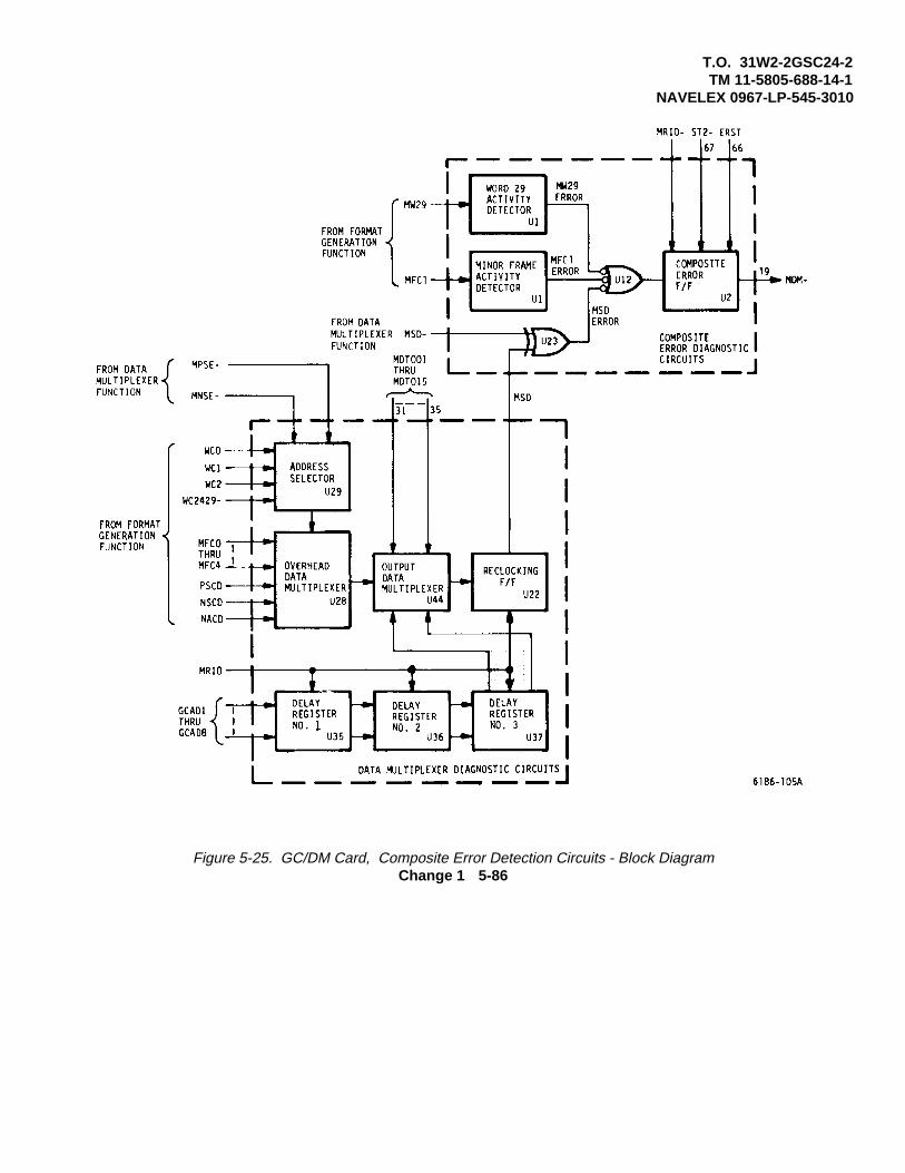
T.O. 31W2-2GSC24-2TM 11-5805-688-14-1
NAVELEX 0967-LP-545-3010
Figure 5-25. GC/DM Card, Composite Error Detection Circuits - Block DiagramChange 1 5-86

T.O. 31W2-2GSC24-2TM 11-5805-688-14-1
NAVELEX 0967-LP-545-3010OR gate U12 sets the composite error flip-flop, whichgenerates data mux diagnostic error signal MDM to thedisplay card. Exclusive OR gate U23 effectivelycompares the MSD output from the functional datamultiplexer circuits with the MSD output from thediagnostic data multiplexer circuits. The diagnostic datamultiplexer circuits are identical to the functional datamultiplexer circuits and produce identical butcomplementary MSD and MSD signals. Therefore, innormal operation, MSD and MSD are complementary toeach other and make exclusive OR gate U23 produce ahigh-level (no error) signal to OR gate U12. If one of thetwo inputs to the exclusive OR gate malfunctions,exclusive OR gate U23 produces a low-level error signalso that signal MDM is generated. Self-test signalST2sets the composite error flip-flop for an errorindication when the SELF TEST switch on the front panelis set to the on (up) position. Error reset signal ERSTresets the flip-flop when the SELF TEST switch on thefront panel is set to the off (down) position or theDISPLAY RESET switch on the front panel is pressed.
5-329. Gated Clock Error Detection Circuits (Figure5-26). In normal operation, four gated clock comparatorssample gated clock signals MGCO1 through MGC15 (Ainput) from the gated clock generation function againstthe same signals (B input) generated by the diagnosticgated clock generation circuits. The diagnostic gatedclock generation circuits are identical to the functionalcircuits and produce gated clock signals that normallyare identical to those produced by the functional circuits.When a malfunction occurs, a mismatch is detected by
one of the four comparators and one of the four A=Binputs to AND gate U9 goes low and sets the gated clockerror flip-flop to generate diagnostic gated clock errorsignal MGC that is applied to the display card. Thegated clock error flip-flop can be set and reset by signalsST2and ERST as explained in paragraph 5-328.
5-330. DETAILED CIRCUIT DISCUSSION.
5-331. Format Generation Function.
5-332. The word counter, consisting of flip-flop U5 andbinary counter U14, is incremented by end-of-scan signalMEOS2B to produce 5-bit binary word counts WCOthrough WC4 that address read only memory (ROM)U20. The word counter counts sequentially until it isreset by word count 29 from flip-flop U3-7 in the words28/29 generator. In the multiplexer function, presetinputs P1 and P2 on binary counter U14 are set to 00 bythe application of signal M+5R through inverter U15.This configuration I)resets the word counter to a count of1 after word 29. In the demultiplexer function, wordcounter preset signal DWPR is applied one time toinverter U15 when synchronization is initially obtained inthe frame sync card. Signal DWPR sets the P1 and P2inputs on binary counter U14 to 11 and also applies apreset signal through OR gate U4, and inverter U13,presetting the counter to a count of 12. After initial resetin the demultiplexer function, the word counter is presetto a count of 1.
5-333. The ROM is programmed to generate six outputsthat are selected by 5-bit word count signals WCOthrough WC4 applied from the word counter. As shownin table 5-5, the ROM outputs are two identical sets ofthe three stuffing codes (PSC, NSC, NAC for thefunctional circuits and PSCD, NSCD, NACD for thediagnostic circuits).
5-87
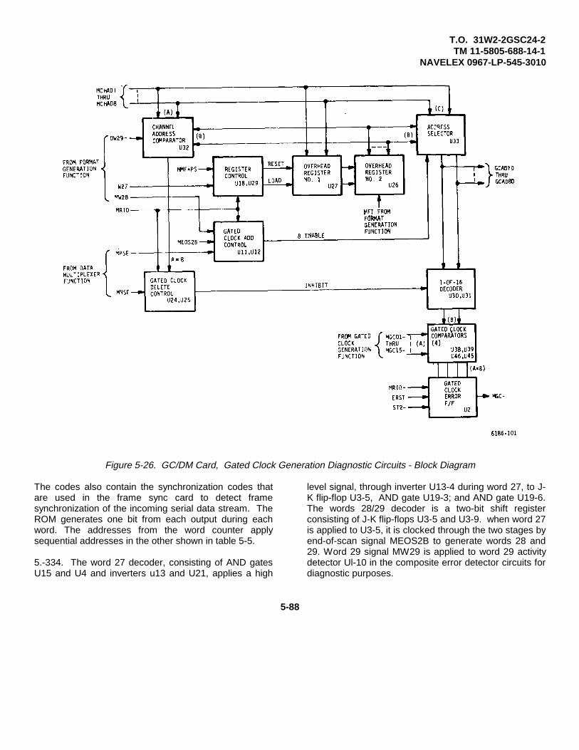
T.O. 31W2-2GSC24-2TM 11-5805-688-14-1
NAVELEX 0967-LP-545-3010
Figure 5-26. GC/DM Card, Gated Clock Generation Diagnostic Circuits - Block Diagram
The codes also contain the synchronization codes thatare used in the frame sync card to detect framesynchronization of the incoming serial data stream. TheROM generates one bit from each output during eachword. The addresses from the word counter applysequential addresses in the other shown in table 5-5.
5.-334. The word 27 decoder, consisting of AND gatesU15 and U4 and inverters u13 and U21, applies a high
level signal, through inverter U13-4 during word 27, to J-K flip-flop U3-5, AND gate U19-3; and AND gate U19-6.The words 28/29 decoder is a two-bit shift registerconsisting of J-K flip-flops U3-5 and U3-9. when word 27is applied to U3-5, it is clocked through the two stages byend-of-scan signal MEOS2B to generate words 28 and29. Word 29 signal MW29 is applied to word 29 activitydetector Ul-10 in the composite error detector circuits fordiagnostic purposes.
5-88

T.O. 31W2-2GSC24-2TM 11-5805-688-14-1
NAVELEX 0967-LP-545-3010
Table 5-5. List of ROM Outputs (Stuff Codes)
DATA WORD (BIT 0 POSITION)
1 2 3 4 5 6 7 8 9 10 11 12 13 14 15 16 17 18 19 20 21 22 23
WORD WC0 1 0 1 0 1 0 1 0 1 0 1 0 1 0 1 0 1 0 1 0 1 0 1COUNTINPUTS: WC1 0 1 1 0 0 1 1 0 0 1 1 0 0 1 1 0 0 1 1 0 0 1 1
WC3 0 0 0 1 1 1 1 0 0 0 0 1 1 1 1 0 0 0 0 1 1 1 1 0 0 0 0 1 1 1 1
WC4 0 0 0 0 0 0 0 0 0 0 0 0 0 0 0 1 1 1 1 1 1 1 1
STUFFCODEOUTPUTS:
PSC Y1, Y4 1 1 0 0 1 1 1 0 1 0 1 1 1 1 1 1 0 1 1 0 1 0 1
NSC Y2, Y5 1 1 0 0 0 0 0 1 0 1 0 1 1 1 0 0 1 0 1 1 0 1 0
NAC Y3, Y6 0 0 1 1 0 0 0 0 1 0 1 0 0 0 1 1 0 1 0 1 0 1 0
5-335. Word 29 signal MW29 and end of-scan signalMEOS2B enable AND gate U4-3 to produce the minorframe transition signal MFT. Signal MFT clocks theminor frame counter consisting of flip-flop U5 and binarycounter U6. The minor frame counter is incremented bysignal MFT until the frame count 31. Signal MMF31, theterminal count from U6, is generated by the binarycounter. Signal MFC1 is applied to minor frame activitydetector U1-6 in the composite error detector circuits fordiagnostic purposes. Multiplexer minor frame countsignals MMFCO through MMFC4 are routed to the seqcard. Minor frame terminal count signals MMF31A-,MMF31B-, and MMF31Care distributed to channel cardlocations Al through A15 for use by the RCB cards.
5-336. Minor frame count signals MFCO through MFC4from minor frame counter U5, U6 are applied tooverhead data multiplexer U50 to identify the used port
that is receiving overhead service in the minor framebeing addressed at any given time.
5-337. Gated Clock Generation Function.
5-338. Channel address signals MCHADO throughMCHAD8 from the sequencer card contain the addressof the active channel selected to receive a gated clocksignal. The channel address signals are applied at themultiplexer clock rate (MRIO) to the inputs of overheadregister No. 1 (U48) and to the C input of addressselector U53. In normal operation, AND gate U12-6 inthe gated clock control circuit is inhibited by the absenceof MPSE. This condition sets flip-flop U11 in the gatedclock add control circuit to generate an enable signal tothe C input of U53.
5-89

T.O. 31W2-2GSC24-2TM 11-5805-688-14-1
NAVELEX 0967-LP-545-3010
In this state, the applied channel address signals arerouted directly through U53 to the inputs of 1-of-16decoder U51, U52. The l-of-16 decoder contains two 1-of8 decoders that decode the four-bit channel addressinto the appropriate gated clock signal (MGCO1 throughMGC15) representing the selected channel address. Inthis normal operating configuration, one gated clocksignal is generated for each channel address clockedinto the circuits.
5-339. overhead service for a given channel address isinitiated when minor frame equals port sequence signalMMF=PS is applied to U18-5 in the register controlcircuit. Signal MMF=PS from the sequencer card is onlyapplied to U18-5 during word 28 of each minor framethat services a used port. During word 27, signal W27and end-of-scan signal MEOS2B initiate the master resetsignal from AND gate U19-3 in the register control circuit.The master reset signal, in turn, resets the output fromoverhead register No. 1 (U48) to 0000 in word 27 ofeach minor frame period. The output from U48 remains0000 during each minor frame period not assigned toservice a used port. When signal MMF=PS isgenerated, a load signal is applied to overhead registerNo. 1, and the channel address (MCHADO throughMCHAD8) applied to the card is loaded into overheadregister No. 1.
5-340. The output from overhead register No. 1 (U48) isapplied to overhead register No. 2 (U54) and to the OEGcard as overhead address count signals MOHO throughMOH3. The channel overhead address count signalsinterrogate the OEG card to see if the selected channelis requesting one of the three overhead serviceconditions: positive stuff, negative stuff, or no action.The OEG card, in turn, applies signal MPSE for apositive stuff condition, signal MNSE for
a negative stuff condition, or neither signal to indicate ano-action condition. When a channel address is appliedto the GC/DM card during a minor frame periodassociated with an unused port, signal MMF=PS is notgenerated, and the channel address from overheadregister No. 1 remains 0000. Channel address 0000 onthe OEG card is an inactive channel; therefore, a noaction condition is reflected back to the GC/DM card.Signal MPSE or signal MNSE is never applied to theGC/DM card in response to channel address 0000. Thechannel address in overhead register No. 1 is clockedinto overhead register No. 2 (U54) by minor frametransition signal MFT. Signal MFT is generated fromAND gate U4-3 when signals MEOS2B and MW29 areapplied to the AND gate. The channel address clockedinto overhead register No. 2 is applied to the B input ofchannel address comparator U47 and to the B input ofaddress selector U53.
5-341. When a positive stuff action is designated for thechannel address being interrogated on the OEG card,signal MPSE is applied to U12-6 in the gated clock addcontrol circuit. Signal MPSE, together with signalsMEOS2B and word 28 (from flip-flop U3-5) enable ANDgate U12-6 so that flip-flop U11, in turn, generates the Benable signal to address selector U53. The B enablesignal enables the B input of U53 so that overheadaddress stored in overhead register No. 2 (U54) isapplied to 1-of-16 decoder U51, U52. The 1-of-16decoder, in turn, generates one additional gated clocksignal during bit 0 of word 29 for the active channeladdress designated for the positive stuff bit.
5-342. When a negative stuff action is designated forthe channel address being interrogated on the OEGcard, signal MNSE is applied to AND gate U24-12 in thegated clock delete control circuit. When signal MFToccurs, the channel address being interrogated on theOEG card is applied through overhead register No. 2(U54) to the B input of channel address comparator U47.
5-90

T.O. 31W2-2GSC24-2TM 11-5805-688-14-1
NAVELEX 0967-LP-545-3010
During word 29, the comparator is enabled and outputsignal A=B is produced when the incoming channeladdress matches the overhead channel address appliedto the B input of the comparator. Signal A=B and signalMNSE are applied to AND gate U24-12. The output fromflip-flop U25 to AND gate U24 is high for one multiplexerclock time (MRIO). AND gate U24, in turn, generates aninhibit to AND gate U16-11 for one clock time. Thiscondition causes a high-level inhibit signal to 1-of-16decoder U51, U52, preventing one gated clock signalfrom being generated for the designated channeladdress. Flip-flop U25 is configured so that only onesignal A=B can enable AND gate U24-12 in word 29 of aminor frame. Otherwise, other used ports strapped tothe selected active channel could also develop anegative stuff condition when the redundant channeladdress appears and is compared with the channeladdress applied to the B input of channel addresscomparator U47.
5-343. Data Multiplexer Function.
5-344. Output data multiplexer U57 combines up to 15channels of output data (MDT001 through MDT015) fromthe active channels in the multiplexer, together with oneoverhead data channel input from overhead datamultiplexer U50. Channel addresses GCAD1 throughGCAD8 from address selector U53 sequentially selectthe data inputs to output data multiplexer U57. Channeladdresses GCAD1 through GCAD8 are routed throughdelay registers No. 1, No. 2, and No. 3 (U49, U55, andU56) to the multiplexer. The three registers provide atime delay that is equal to three multiplexer clocks(MRIO) to compensate for the time delay in the data TTLcircuit applications. The channel addresses applied fromU56 to data output multiplexer U57 sequentially selectone overhead data bit from overhead multiplexer U50
and one bit from each of the channel data inputs(MDT001 through MDT015) applied from the activechannel cards. The single serial data stream frommultiplexer U57 is applied through inverter U13-12 toreclocking flip-flop U22. Complementary serial datastreams MSD and MSD are clocked out of U22 at themultipliexer clock MRIO rate. Signal MSD is routed tothe reference timer card and signal MSD is applied to thecomposite error detection function.
5-345. Overhead data multiplexer U50 combines theoverhead data inputs for a selected port into the serialoverhead data format that is applied to one input ofoutput data multiplexer U57 during bit 0 of words 1through 28 in each minor frame period. The serialoverhead data contains one of the three stuff commandsignals (PSC, NSC, and NAC) in bit 0 of words 1through 23 of each minor frame. Bit 0 of words 24through 28 of each minor frame contains the 5-bit binarycode for the port receiving overhead service during agiven minor frame. Positive stuff command signal MPSAand negative stuff command signal MNSA from the OEGcard are applied through three AND gates U34 topositive stuff latch U42-10 and negative stuff latch U42-6. At the end of each minor frame, the selected stuffcommand is clocked into the appropriate latch by minorframe transition signal MFT from AND gate U4-3. Whena positive stuff condition is initiated, latch U42-9produces signal MPSE, which is applied to U12-6 (pin 70strapped to pin 89) in the gated clock generation circuits,and U49-10 produces signal PSE-, which is applied tothe C input of address selector U43. Initiation of anegative stuff generates signal MNSE from latch U42-7,which is applied to U24-12 (pin 29 strapped to pin 87) inthe gated clock generation circuits, and U42-6 producessignal NSE-, which is applied to the C input of addressselector U43.
5-91

T.O. 31W2-2GSC24-2TM 11-5805-688-14-1
NAVELEX 0967-LP-545-3010
For a no action condition, neither signal MPSA norMNSA is generated. Therefore, signals MNSE andMPSE are not generated and signals PSE and NSE arehigh-level inputs to the C input of address selector U43.
5-346. The absence of word count signalWC2429enables the B input of U43 during words 1through 23. During words 1 through 23, one 3-bit stuffcommand code is applied through U43 to the data selectinputs of overhead data multiplexer U50. The 2-bit stuffcode enables the data inputs at pin 6, 7, or 9 so that theappropriate stuff code (NAC, NSC or PSC) is routedthrough multiplexer USO0 to input IO of output datamultiplexer U57. The 3-bit binary stuff command codesthat can be applied during words 1 through 23 are shownbelow.
5-347. Word count signal WC2429enables the B input ofU43 during words 24 through 29. Five sequential binaryaddresses derived from word count signals WC0, WC1,and WC2 are applied through the B input of U43 to thedata select inputs of overhead data multiplexer U50.The WCO, WC1, and WC2 codes applied during words24 to 29 are 000 (enables pin 1 on U50) through 101(enables pin 5 on U50). Minor frame count signalsMFCO through MFC4 from minor frame counter U5, U6are applied in reverse order to input pins 1 through 5 ofU50. The most significant digit (signal MFC4) is appliedto pin 1 (first bit sampled), and the least significant digit(signal MFCO) is applied to pin 5 (last bit sampled). The
reverse binary code read out of US0 during bit 0 of words24 through 28 identifies the used port being servicedduring the minor frame identified in the frame countsignals at the output of counter US, U6. For example,minor frame 3 (count 00011 from U5, U6) services port24 (count 11000 from U50).
5-348. Diagnostic Function.
5-349. Composite Error Detection Circuit. A low-levelinput to any one of the three inputs to OR gate U12-8places a high-level signal to the input of error flip-flop U2.The flip-flop, in turn, produces data mux diagnostic errorsignal MDM- when the next multiplexer clock signalMRIO- clocks the flip-flop. Two of the inputs to OR gateU12 are provided from word 29 activity detector U1-10and from minor frame activity detector U1-6. Bothactivity detectors are retriggerable multivibrators that areheld in conduction by the word 29 signals (MW29) orminor frame signals (MFC1). When the signal ismissing, the stage will complete its duty cycle andproduce a low-level error signal to OR gate U12. Thethird input to OR gate U12 is from exclusive OR gateU23-6, which samples signal MSD from the functionaldata multiplexer circuit and diagnostic signal MSD fromthe diagnostic equivalent circuits. When a malfunctionoccurs, signals MSD and MSD- will eventually compareand cause the exclusive OR gate to generate a low-levelerror signal to OR gate U12.
3-Bit Address CodeSignal to Latch U42 to U50 From U43 Stuff Input to U50
S0 S1 S2
MPSA (positive stuff) 1 0 1 Pin 6 (PSC)MNSA (negative stuff) 0 1 1 Pin 7 (NSC)Neither (no action) 1 1 1 Pin 9 (NAC)
5-92

T.O. 31W2-2GSC24-2TM 11-5805-688-14-1
NAVELEX 0967-LP-545-3010
5-350. Gated Clock Error Generation Circuit. The gatedclock error generation circuit consists of four 8inputcomparators U45, U38, U46, and U39 that provide fourA=B outputs to AND gate U9-8, which, in turn, provides asignal to the input of gated clock error flip-flop U2. Whenthe 15 gated clock outputs (MGCO1 through MGC15)from function 1-of-16 decoder U51, U52 compare withthe gated clocks from the diagnostic 1-of-16 decoderU30, U31, four high-level signals A=B hold AND gate U9-8 in conduction so that a low-level signal is applied to theinput of flip-flop U2. When one or more of the functionalgated clocks in one of the comparators do not comparewith the diagnostic gated clocks, the A=B output goeslow and inhibits AND gate U9. In turn, AND gate U9places a high to the input of flip-flop U2 so that gatedclock error signal MGC is produced the next time signalMRI0-clocks the flip flop. Both error flip-flops U2-6 andU2-7 can be set to the self-test state by self-test signalST2and can then be reset by signal ERST.
5-351. OVERHEAD ENABLE GENERATOR OEGCARD.
5-352. GENERAL.
5-353. The OEG card is one of the common cards. TwoOEG cards are used in the multiplexer set: one in themultiplexer and one in the demultiplexer. The blockdiagram for the circuits described in the block diagramdiscussion is shown in figure 5-27. The logic diagramassociated with the detailed circuit discussions iscontained in the circuit diagrams manual.
5-354. In the multiplexer, the OEG card performs threefunctions. First, the OEG card accepts positive andnegative stuffing requests from the active channel cardsand then multiplexes the positive stuffing requests intoone positive stuff acknowledge output stream, and thenegative stuff requests into one negative stuffacknowledge output stream. The two serial outputstreams are routed to the GC/DM card for overheadservicing. During word 24 the positive stuff acknowledgestream contains the diagnostic status for the channelcards. This data is routed to the display card as part ofthe diagnostic function during word 24. Second, systemclock signal R0 from the reference timer card is applied tothe OEG card, which then redistributes the signal asmultiplexer system clock signals MRIO1through MRI08toother cards in the multiplexer. Third, the OEG cardgenerates word 24, word 24 end of scan 2, word 24 bit0, and end-of-scan (EOS) signals by decoding signalsfrom the word counter and end-of-scan logic. The signalsare then routed to the channel cards and to the displaycard for timing purposes.
5-355. In the demultiplexer, the negative stuff requestcircuits are not used on the OEG card. The positive stuffrequest lines are used only for the diagnostic datarequired for the diagnostic function on the display card.
5-356. BLOCK DIAGRAM DISCUSSION.
5-357. In the multiplexer, positive stuff request signalsMPST01through MPST15from the channel cards areapplied through the ON positions of the DIAGNOSTICSAND OVERHEAD switches to positive stuff multiplexerNo. 1 Negative stuff request signals MNST01throughMNST15are applied to negative stuff multiplexer No. 1.
5-93

T.O. 31W2-2GSC24-2TM 11-5805-688-14-1
NAVELEX 0967-LP-545-3010
Figure 5-27. OEG Card - Block Diagram5-94

T.O. 31W2-2GSC24-2TM 11-5805-688-14-1
NAVELEX 0967-LP-545-3010
Overhead address count signals MOH0 through MOH3from the GC/DM card contain the 4-bit channeladdresses that select the one channel to be interrogatedin both multiplexers during each minor frame. Positiveand negative stuff acknowledge signals MPSA andMNSA from the two multiplexers are routed back to theGC/DM card as part of the overhead function. Positivestuff acknowledge signal MPSA from positive stuffmultiplexer No. 1 is routed to the display card, where thesignal is interrogated for diagnostic error data duringword 24. Self-test signal ST2 is applied through the OFFpositions of the DIAGNOSTICS AND OVERHEADswitches to the inactive channel inputs of positive stuffmultiplexers No. 1 and No. 2 to prevent false diagnosticerror indications during the self-test mode.
5-358. The word 24 decoder generates word 24 signalswhen word count signals MWC0, MWC1, MWC2 andMWC4 from the GC/DM card are a count 23 and end of-scan signal EOS2 from the end-of scan decoder isgenerated. The output signals from the decoder areword 24 signals MW24N1through MW24N4 and word 24bit 0 signals MW2401through MW2404-. The outputsignals are applied to the channel cards and to the framesync card. Word 24 end-of-scan signal M24EOS2 fromAND gate U21 is generated and routed to the displaycard when the two decoder circuits generate word 24and EOS2.
5-359. The end-of-scan decoder generates end-of-scansignals EOS2, and EOS3 that represent two levels of theend-of-scan signal. Each sequential EOS signal isseparated in time by one R clock time. Signal EOS2 isapplied to AND gate U21 and to word 24 decoder as anenable signal. End-of scan signals MEOS3N1 throughMEOS3N4 generated by the decoder are routed to thechannel cards.
5-360. System clock signal Ro is applied through systemclock buffers and is distributed as system clock signalsMRIO1through MRI08to the channel cards. Clock signalMRIO is also derived from signal Ro and is applied to theGC/DM and sequencer cards.
5-361. Positive stuff multiplexer No. 2 and negative stuffmultiplexer No. 2 are part of the diagnostic function. Thetwo multiplexers duplicate the outputs of positive andnegative stuff multiplexers No. 1. Diagnostic stuffacknowledge MPSA and MNSA signals from the twodiagnostic multiplexers are applied to the diagnosticcomparator, where they are compared with thefunctional MPSA and MNSA outputs. When the outputsignals being compared are not alike, the diagnosticcomparator generates a stuff error signal to thecomposite error detector. The composite error detector,in turn, generates OEG card diagnostic signal MTMOGas described in paragraph 5-364.
5-362. The system clock activity detector monitorssystem clock signal Ro and generates diagnostic loss-oftiming error signal MLOT when the signal is missing.Once the error condition is detected, signal MLOT isapplied to the display card until the DISPLAY RESETswitch on the front panel is pressed. When the switch ispressed, reset signal ERST is applied to the detector. Ifthe malfunction is corrected, the detector returns to itsno-error state. When the SELF TEST switch on the frontpanel is set to the on (up) position, self-test signal ST2isapplied to the card and the detector is set to its errorposition until the SELF TEST switch is returned to the off(down) position. When the SELF TEST switch is set tothe off (down) position, reset signal ERST isautomatically applied to the card and the detector is resetto its no-error state.
5-95

T.O. 31W2-2GSC24-2TM 11-5805-688-14-1
NAVELEX 0967-LP-545-3010
5-363. The word 24 activity detector monitors the word24 output from the word 24 decoder and generates aword 24 error signal to the composite error detectorwhen either the word 24 decoder or end-of-scan decodersignals are missing. The detector can be set or reset bysignal ST2 or ERST as explained in paragraph 5-362.
5-364. The composite error detector generates OEGcard diagnostic signal MTMOG to the display card whena stuff error or W24 error signal is applied. Once theerror input to the detector is removed, the detector outputreturns to its no-error state. The detector circuits can beset to the error state by self-test signal ST2- as explainedin paragraph 5-362.
5-365. DETAILED CIRCUIT DISCUSSION.
5-366. In certain unique system configurations, achannel may possibly be active but not have a channelcard installed. Therefore, the 15 DIAGNOSTICS ANDOVERHEAD switches (S1) are provided on the OEGcard to prevent false channel card diagnostic errorsignals when the multiplexer is in the self-test mode.The switch is set to the ON position for each activechannel that has a channel card installed. In turn, theswitch associated with each active channel not having achannel card installed is set to the OFF position.Settings of switches associated with inactive channelsmay be in the ON or OFF positions, since inactivechannels are not sampled. In the self-test mode, eachchannel input to positive stuff multiplexer U3 that has theswitch in the ON position receives the diagnostic errorstatus from the associated channel card. Each channelcard input to multiplexer U3 that has the switch set in theOFF position receives a low-level self test signal ST2inthe self-test mode, and a high-level no-error signal innormal operation. A low-level diagnostic signal input tomultiplexer U3 is processed as a no-error condition in theoverhead diagnostic function. Without the
DIAGNOSTICS AND OVERHEAD switching capability,an active channel not fitted with a channel card wouldyield a high-level error signal, which would be applied tothe channel input of multiplexer U3 to indicate a faultydiagnostic-error condition during the self-test mode.Setting the appropriate DIAGNOSTICS ANDOVERHEAD switches to the OFF positions for thesechannels prevents an undesirable self-test condition.
5-367. Positive stuff request signals MPSTO1throughMPST15from the active channels in the multiplexer areapplied through the ON positions of the switches (S1) toinputs on positive stuff multiplexer No. 1 (U3). Overheadaddress count signals MOHO through MOH3 select themultiplexer channel that is interrogated and multiplexedinto a single positive stuff output data stream as positivestuff acknowledge signal MPSA. Signal MPSA is routedto the GC/DM card. The signal is also applied toexclusive OR gate U8-6 in the diagnostic comparatorcircuit. As part of the card diagnostic function performedduring word 24, signal MPSA is applied through .inverterU7-3 and is routed as signal MPSA to the display card.Negative stuff request signals MNSTO1throughMNST15are processed through negative stuffmultiplexer No. 1 (U5) to generate a single negative stuffoutput data stream as negative stuff acknowledge signalMNSA. Signal MNSA is routed to the GC/DM card.
5-368. Signals MPSA and MNSA are compared in thediagnostic comparator circuit with their equivalentdiagnostic MPSA and MNSA signals from positive andnegative stuff multiplexers No. 2 (U4 and U6). Thecompare function is performed by four exclusive ORgates (U8). When an error condition is detected(mismatch), the exclusive OR gates cause flip-flop U15to generate a high-level Q output which, in turn, causesOEG card diagnostic signal MTMOG- to be generatedfrom OR gate U13-4 in the composite error detectorcircuit.
5-96

T.O. 31W2-2GSC24-2TM 11-5805-688-14-1
NAVELEX 0967-LP-545-3010
5-369. System clock signal Ro from the reference timercard is applied through a series of inverters (U20 andU24) to produce system clock signals MRIO andMRIO1through MRI08-. Retriggerable one-shotmultivibrator U12-10 in the system clock activity detectorcircuit is held in conduction by signal Ro. When Ro ismissing, the one-shot multivibrator’s duty cycle expiresand its output sets latch U7, which, in turn, generatesloss of timing signal DLOT- that is applied to the displaycard. The latch remains set until reset signal ERST isapplied when the DISPLAY RESET switch on the frontpanel is pressed.
5-370. When word count 23 is applied to AND gate U16-6 by word count signals MWC0, MWC1, MWC2, andMWC4, and end-of-scan signal EOS2 from U23-5 isapplied to clock flip-flop U18-6, the word 24 signal isgenerated. The word 24 signal is buffered anddistributed through inverters U14 and U19 as word 24signals MW24N1through MW24N4- to the channelcards. The output from U18-6 is also applied to ANDgate U21-11, which, in turn, produces signal M24EOS2when end-of-scan signal EOS2 is applied at its otherinput from flip-flop U23-5 during word 24. AND gate U16-8 also produces a word 24 output when the word 24output from U18-6, EOS3 from U18-7, and Ro arepresent. The pulsed output from AND gate U16-8 isapplied to the four U22 inverters to produce word 24 bit 0signals MW2401through MW2404-. These signals arealso routed to the channel cards.
5-371. End-of-scan signal MEOS is clocked through twostages of flip-flop U23 by R to generate end-of-scan
+ 2 bits signal EOS2 for U18-6 in the word 24 detectorcircuit. Signal EOS2 is also clocked through U18-9 toproduce end-of-scan +3 bits signal EOS3. Signal EOS3from flip-flop U18-9 is buffered through the three U19inverters and inverter U22 to produce end-of-scan 3signals MEOS3Nl through MEOS3N4 for the channelcards.
5-372. Setting the SELF TEST switch on the front panelto the on (up) position applies self-test signal ST2to thecard. Signal ST2- inhibits retriggerable multivibratorU12-7 in the word 24 activity detector circuit, which setslatch U13 so that a high level error signal is applied toAND gate U9-8 in the composite error detector circuit.Retriggerable multivibrator U12-10 in the system clockactivity detector circuit is also inhibited by ST2- so thatlatch U7 is set to produce diagnostic loss of timing errorsignal DLOT-. In the self test mode, during word 24, allthe active inputs to the four multiplexers are low. SignalST2- is applied through the three U11 inverters and theOFF positions of DIAGNOSTICS AND OVERHEADswitch S1 to place a low level signal on each of theunused inputs of the two positive stuff multiplexers. Thisconfiguration ensures a continuous high input to each ofthe four exclusive OR gates (U8) in the comparatorcircuit. Signal ST2- places a high-level signal to oneinput of exclusive OR gates U8-3 and U8-11. The resultis a high-level error signal from J-K flip-flop U15-7 in thecomparator circuit to AND gate U9-8 in the compositeerror detector circuit. The three high-level inputs to ANDgate U9 result in the generation of low-level OEG carddiagnostic signal MTMOG from OR gate U13-4 in thecomposite error detector circuit. Reset signal ERST isapplied to the card when the SELF TEST switch on thefront panel is set to the off (down) position or theDISPLAY RESET switch on the front panel is pressed.Signal ERST resets the two diagnostic latch circuits (U7and U13) and forces J-K flip-flop U15-7 to reset andreturn the diagnostic circuits to their functional no-errorstate, assuming that there are no malfunctions on thecard.
5-97

T.O. 31W2-2GSC24-2TM 11-5805-688-14-1
NAVELEX 0967-LP-545-3010
5-373. REFERENCE TIMER (RT) CARD.
5-374. GENERAL. The reference timer card is one ofthe common cards used in the multiplexer. The cardgenerates system clock signal Ro that is applied to theOEG card, which, in turn, duplicates and distributes themaster clock signal as multiplexer clock signal MRIO tothe multiplexer cards. The card accepts the multiplexedserial digital data (MSD) from the GC/DM card, developsthe multiplexer timing out signal TIMOUT, and clocks theassociated timing data and timing pulses from the cardat the selected Ro rate. Timing signals T3600 andT4800, generated on the card, are routed to thetransition encoder cards in the multiplexer. The blockdiagram for the circuits described below are shown infigures 5-28 and 5-29. The logic diagram associated withthe detailed circuit discussion is contained in the circuitdiagrams manual.
5-375. BLOCK DIAGRAM DISCUSSION.
5-376. System clock signal Ro is developed fromexternal multiplexer timing signals (TIMIN) that areapplied to the line receiver circuits (figure 5-28) or from amaster oscillator on the card. The input to be used fordeveloping Ro selected by strapping switch S5 to its INTor EXT position. The signals through S5 are applied tothe 15-stage binary counter and to the loss-of-timingactivity detector. Switch S6 is strapped to position 1(output of S5) when the selected Ro is the samefrequency as the source frequency. The switch isstrapped to one of the positions 2 through 16 when the
Ro selected is a binary quotient of the source frequency.Signal Ro through S6 is applied to the system clockbuffer and to the phase-adjust circuit. The Ro outputfrom the buffer is applied to the data retiming flip-flop,system clock activity detector and to the OEG card. Thephase adjust circuit contains a factory adjustment (S3)that phases the timing output signals (TIMOUT andTIMOUT-) to the serial digital data outputs (SDATAO andSDATAO-). The data and timing output signals from theline switches can be applied to a balanced or unbalancedline. When the system is used in a balancedconfiguration, the output data and timing line switchesare set so that the two data signals and the two timingsignals are applied to balanced lines. When the systemis used in an unbalanced configuration, the output dataand timing line switches are set so that the SDATAO andTIMOUT-signal outputs are inhibited by connecting theiroutput pins to ground.
5-377. The timing error detectors monitor the TIMOUTand TIMOUT-output voltages, and detectors generate adiagnostic error signal to the composite OR gate andlatch circuits when a malfunction is detected. Thecomposite OR gate and latch circuits also have errorsignal inputs from the 3600Hz and 4800-Hz activitydetectors in the transition encoder timing circuits on thecard. The five diagnostic error inputs are ORed together,and when any one of the inputs contains an errorcondition, the error signal sets the latch circuit togenerate reference timer diagnostic signal MRT that isapplied to the display card. The loss of-timing activitydetector error output is set when the timing signalthrough S5 is missing. Reset signal ERST resets theerror detection circuits back to their no-error state whenthe DISPLAY RESET switch on the front panel ispressed. Diagnostic signals MLOT and MRT areproduced to represent error conditions when the SELFTEST switch on the front panel is set to the on (up)position and self test signal ST2is applied to the errordetection circuits.
5-98

T.O. 31W2-2GSC24-2TM 11-5805-688-14-1
NAVELEX 0967-LP-545-3010
Figure 5-28. RT Card, Data and Timing Circuits - Block Diagram
Setting the SELF TEST switch to the off (down) positionapplies reset signal ERST to the circuits and forces themto their no-error state.
5-378. The transition encoder timing circuits (figure 5-29) generate timing signals T3600 (3600 Hz) and T4800(4800 Hz) that are used by the TE/TR channel cards inthe multiplexer. The timing oscillator generates a1.8432MHz (+0.01 percent) timing signal that is applied
to an eight-stage ¸ 2n binary counter. The N=8 (7.2 kHz)output from the counter is applied to the divide-by-twocounter, which, in turn, supplies the 3600-Hz timingsignals to the 3600-Hz distribution buffers. Thedistribution buffers produce 3600-Hz timing signalsT3600A, T3600B, and T3600C that are routed to thechannel card locations.
Change 1 5-99

T.O. 31W2-2GSC24-2TM 11-5805-688-14-1
NAVELEX 0967-LP-545-3010
Figure 5-29. RT Card, Transition Encoder Timing Circuits - Block Diagram
The N=6 (28.8 kHz) output from the eight-stage ¸ Nbinary counter is applied to the divide-by six counter,which, in turn, supplies the 4800-Hz timing signals to the4800-Hz distribution buffers. The distribution buffersproduce 4800-Hz timing signals T4800A, T4800B, andT4800C that are routed to the channel card locations.The 3600-Hz and 4800Hz activity detectors sample thetiming signals and generate diagnostic error signals to
the composite OR gate and latch circuits on the cardwhen timing signals T3600A and T4800A are missing.The two activity detector circuits are set and held in theerror state by self-test signal ST2 when the SELF TESTswitch on the front panel is set to the on (up) position.When the SELF TEST switch is set to the off (down)position, signal ST2 is removed and the activity detectorcircuits return to their no-error state.
Change 5-100

T.O. 31W2-2GSC24-2TM 11-5805-688-14-1
NAVELEX 0967-LP-545-3010
5-379. DETAILED CIRCUIT DISCUSSION.
5-380. Timing Circuits.
5-381. System clock signal Ro is developed from timingsignals TIMIN and TIMIN-, which are applied from anexternal source, or Ro is developed from timing oscillatorY1 on the card. Selection of the timing source is madeby strapping switch S5 to its EXT or INT position. Theoscillator is a plug-in module that provides one basefrequency selected for a given system application. Theoscillator or the external timing input frequency isselectable within the range of 155 Hz to 10 MHz.However, the 15-stage binary counter permits a sourcesignal within the range of 5 MHz to 10 MHz to cover all ofthe desired frequencies within a given systemconfiguration. When the external source is used, theTIMIN and TIMIN signals are applied to differential linereceiver U8. The line receiver processes the incomingdigital timing signals into TTL logic levels, which, in turn,are applied to switch S5. The signals through S5 areapplied to the first stage of the 15 stage binary counter,to switch position S6-1, and to one-shot multivibrator U10in the loss-of-time activity detector.
5-382. The timing signals through switch S5 are routedthrough inverter U3 to J-K flip-flop U1 in the 15-stagebinary counter. The four J-K flip-flops (U1, U4) performa high-speed divide-by-16 of the incoming timing signalsto provide outputs to pins 2 through 5 of switch S6.Four-bit binary counters U6, U7, and U2 perform divide-by-32 through divide-by-32768 of the incoming timingsignals to provide outputs to pins 6 through 16 on switchS6. The timing output signal strapped through switch S6is system clock signal Ro that is applied to inverter U3 inthe phase-adjust circuit. Signal Ro is also routed throughinverters U5, which perform a buffer function, to the OEGcard.
5-383. Switch S3 in the phase-adjust circuit is factory
preset. The switch is set so that timing out signalsTIMOUT and TIMOUT are in phase with the serial digitaldata output pulses (MSD) as shown in figure 5-30. Thetiming signals from the phase-adjust circuit are appliedthrough polarity switch S1 to amplifiers Q1 and Q2 in thetiming output drivers circuit. Polarity switch S1 is used insystem configurations to change the polarity of the timingpulses with respect to the digital data pulses. TransistorQ3 is a constant current source for amplifiers Q1 andQ2. Amplifiers Q1 and Q2 in turn, drive push-pullemitter-followers Q4 through Q7. Setting switch S2 tothe balanced position (B) connects breakdown diodesVR2 and VR4 (2.4 vdc) in parallel with breakdown diodesVR3 and VR5 (5.6 vdc) in the base circuit of emitter-followers. This balanced configuration producesbalanced +3-volt TIMOUT and TIMOUT signals. SwitchS2 in the unbalanced position (U) connects onlybreakdown diodes VR3 and VR5 into the base circuit ofthe emitter-followers so that a +6-volt TIMOUT signal isgenerated and TIMOUT signal output from the card isgrounded. Diodes CR2 and CR3 in the collector circuitsof Q1 and Q2
Figure 5-30. RT Card, Reference Timing - WaveformDiagram
5-101

T.O. 31W2-2GSC24-2TM 11-5805-688-14-1
NAVELEX 0967-LP-545-3010
provide sharp cutoff and turn-on characteristics for thepush-pull emitter followers.
5-384. The RC time constant of retriggerable one-shotmultivibrator U10 in the loss-of-timing activity detector islong enough that the continuous timing pulses throughS5 can hold the stage in conduction. When the timingsignals are interrupted, U10 completes its duty cycle andits output sets latch U13. Setting latch U13, in turn,produces diagnostic loss-of-timing error signal MLOTthat is applied to the display card. Self-test signal ST2-is applied to set latch U13 when the SELF TEST switchon the front panel is set to the on (up) position. Resetsignal ERST to the latch circuit is applied when the SELFTEST switch is set to the off (down) position. SignalERST is also generated when the DISPLAY RESETswitch on the front panel is pressed and then released.When error signal MLOT is generated, the LOSS OFMUX TIMING indicator on the front panel lights andremains lighted until signal MLOT- is removed.
5-385. Transistors Q8 and Q9 in the timing errordetector circuit are normally off and Q10 is conducting.When signal TIMOUT or the TIMOUT is missing, avoltage unbalance occurs that forces either Q8 or Q9into conduction. When Q8 or Q9 conducts, Q10 isforced into cutoff. When Q10 is cut off, a high-leveldiagnostic error signal is applied from Q10 to gates U19and U20 in the composite OR gate and latch circuit.Self-test signal ST2is applied to Q10 when the SELFTEST switch on the front panel is set to the on (up)position. Signal ST2forces Q10 into cutoff and asimulated error signal is applied to the composite ORgate and latch circuits to test the diagnostic circuitfunction. Transistor Q10 is forced into conduction whenthe SELF TEST switch is set to the off (down) position.
5-386. Data Retiming Circuits.
5-387. The multiplexed serial data (MSD) is clockedthrough flip-flop U12 by system clock signal R The dataare routed through polarity switch S7 to the data outputdrivers circuit that generates the balanced or unbalancedserial data out signals SDATAO and SDATAO-. Theoperation of the data output drivers circuit (Q11 throughQ17) is functionally the same as that described for thetiming output drivers circuit. When switch S8 on the cardis set to the unbalanced position (U), output signalSDATAO is tied to ground and SDATAO is +6 vdc.When S8 is in the balanced condition (B), signalsSDATAO and SDATAO are +3 vdc signals.
5-388. The operation of data error detectors Q18through Q20 is functionally the same as that describedfor the timing error detector circuit. A defective outputdata signal generates a diagnostic error signal from Q20to the composite OR gate and latch circuits.
5-389. Transition Encoder Timing Circuits. Timingoscillator Y2 generates 1.8432-MHz (+0.01 percent)timing signals that are applied to eight-stage N binarycounter Ull, U14. The N=6 (28.8 kHz) output from U14-13 is applied to divide-by-six counter U16, U18 toproduce the 4800-Hz timing signals. These signals arerouted through three distribution buffer gates U21 toprovide the T4800A, T4800B, and T4800C timingoutputs. The N=8 (7.2 kHz) output from U14-11 isapplied to divide-by-two counter U16 to generate the3600-Fz timing signals. These signals are routedthrough three distribution buffer gates U24 to provide theT3600A, T3600B, and T3600C timing outputs. Timingsignals T3600A and T4800A are applied to one-shotmultivibrators U10 and U15 in the 3600-Hz and 4800-Hzactivity detectors. When one of the timing signals isinterrupted, the associated multivibrator completes itsduty cycle and a diagnostic error signal is applied tocomposite OR gate U17, causing signal MRT to begenerated as explained in the following discussion.
5-102

T.O. 31W2-2GSC24-2TM 11-5805-688-14-1
NAVELEX 0967-LP-545-3010
5-390. Composite OR Gate and Latch Circuits.
5-391. Latch U20, U23 generates diagnostic referencetimer card error signal MRT when an error is detected orwhen self-test signal ST2is applied to the card. LatchU20, U23 is reset by signal ERST from the front panel aspreviously described.
5-392. The three retriggerable one-shot multivibrators(U10-9, U15-6, and U1510) are normally held inconduction by timing signals T3600A and T4800A andsystem clock signal Ro. An error condition (loss of signal)to any one of the multivibrators causes the appropriatemultivibrator’s duty cycle to expire and set latch U20,U23 through OR gate U17 and AND gate U20. A high-
level error signal from the timing or data diagnosticcircuits applied to OR gate U19 sets the latch to the errorcondition through OR gate U17-6 and AND gate U20-3.
5-393. When the system is in the self-test mode, self-test signal ST2inhibits AND gate U20-3 to prevent anysimulated error inputs from OR gate U17-6 from settinglatch U20, U23. Signal ST2forces the diagnostic circuitsto generate high-level inputs to AND gate U17-8 whenthe card diagnostic circuits are operational. AND gateU17, in turn, sets latch U20, U23, thus generating signalMRT-. When the SELF TEST switch on the front panelis set to the off (down) position, signal ST2goes high(diagnostic enable) and signal ERST resets latch U20,U23 to its no error state.
SECTION IV
DEMULTIPLEXER CARDS FUNCTIONAL OPERATION
5-394. INTRODUCTION.
5-395. This section contains the block diagram anddetailed circuit discussions for each of the card typesused in the demultiplexer. The detailed circuit discussionfor each card follows the associated card-level blockdiagram discussion. The following cards are describedin this section.
Channel Cards Paragraph
SB card 5-396NBSB card 5-419TD card 5-426VD card 5-444
Common Cards Paragraph
Seq card 5-460GC/DM card 5-463OEG card 5-468FS card 5-472ERD card 5-535
5-396. SMOOTHING BUFFER (SB) CARD.
5-397. GENERAL. The SB card is a channel optioncard that may be used to service one data outputchannel with its associated timing. The SB card functionis basically the complement of the RCB card functionperformed in the multiplexer. Functionally, the SB carddemultiplexes one channel of data out of the high-speeddata stream from the far-end multiplexer.
5-103

T.O. 31W2-2GSC24-2TM 11-5805-688-14-1
NAVELEX 0967-LP-545-3010
The data are converted from a synchronous format intothe original asynchronous format that was applied to thefar-end multiplexer. The original timing associated withthe data is also regenerated. The block diagramdiscussions are based on the block diagram shown infigure FO-4. The detailed circuit discussions are basedon the SB card logic diagram in the circuit diagramsmanual.
5-398. BLOCK DIAGRAM DISCUSSION.
5-399. GENERAL. The SB card can be operated in oneof two modes of operation. The mode of operation iscontrolled by setting the URD/SB switch to the URD orthe SB position. The mode of operation is determined bythe mode of operation selected for the far-end RCB cardin the multiplexer function. The system requirementsthat control the mode of operation selected are describedin the RCB card discussion in paragraph 5-169. Asdescribed in the following paragraphs, the basicoperation of the SB card is the complement (or reverse)of the RCB card. The data elastic storage register in theSB card writes in the data under control of asynchronous clock and reads out these data undercontrol of an asynchronous clock. This synchronous toasynchronous form conversion is accomplished using asmoothing function that produces output data bits at thesame rate at which the data were applied to the RCBcard of the far-end multiplexer. This basic smoothingconcept is described in paragraph 5-64.
5-400. Input-Output Buffer Function. The incomingchannel data bits (DTIX-) are clocked through the datainput buffer by associated gated clock signals DGCXX.The gated clock signals are applied directly to the datainput buffer in the SB mode of operation, or the signalsare processed through the coarse rate conversion
circuits when the circuits are operated in the URD modeof operation. The write address counter, which issequentially incremented by gated clock signals DGCXX,generates the 4-bit write addresses that are applied tothe data elastic storage register and to the write addresslatch. The write address signals applied to the dataelastic storage register control the memory locations inwhich the applied data bits are stored. The data elasticstorage register is identical to the data elastic storageregister in the RCB card and has the same write andread capability. The read address counter that generatesthe 4-bit read addresses to the data elastic storageregister is clocked by the read clock signals from theanalog phase-locked loop (APLL) circuit. The dataclocked out of the data elastic storage register areclocked through the data output buffer to the data outputdrivers. The output clock signals that clock the datathrough the data output buffer are also generated by theAPLL circuits. The timing output drivers are also clockedby the output clock signals from the APLL circuit. Thedata and timing output signals are conditioned in theoutput drivers and are routed through their associatedoutput line switch circuits that are set to produce abalanced or an unbalanced line output. When the outputis applied to a balanced line configuration, the outputdata and timing line switches are set so that the twochannel data out signals (DOXX and DOXX-) and thetwo timing out signals (TOXX and TOXX-) aregenerated. In an unbalanced condition, only signalsDOXX and TOXX are generated. The end-of-scanactivity detector samples end-of-scan signal DEOS3NX.The detector is a retriggerable one shot multivibrator thatis held in conduction by signals DEOS3NX. When thesignals are missing, the one-shot multivibrator duty cycleexpires and generates an inhibit signal that inhibits thedata output of the data output buffer.
5-104

T.O. 31W2-2GSC24-2TM 11-5805-688-14-1
NAVELEX 0967-LP-545- 30115-401. APLL Circuit. The write and read addresscounters are clocked by independently generated timingsignals. The write address counter is clocked by gatedclock signal DGCXX, and the read address counter isclocked by the divided output of a voltage-controlledmultivibrator (VCM). The APLL circuit phase locks theoutput of the VCM with the incoming gated clock signal,causing the VCM to generate a number of read clockpulses equal to the number of write clock pulses beingapplied to the data elastic storage register over a givenperiod of time. A smoothing function is alsoaccomplished by the APLL circuit. Gated clock pulsesare added and deleted as a result of the overheadservicing function. The addition or deletion of a gatedclock pulse represents an instantaneous change in theapplied gated clock frequency. Since synchronizationcircuits of user equipment cannot operate with such achange applied to their inputs, instantaneous bit ratedeviation is not acceptable. The APLL circuit thereforedetects the instantaneous gated clock addition ordeletion, and gradually (smoothly) increases ordecreases the output rate of the VCM by one bit timeover an extended number of VCM clock times. Thegradual change in VCM output rate causes the gatedclock and VCM rates to become nominally equal, whileprecluding unacceptable short-term rate variations in thechannel’s output timing signal. Thus, in performing thesmoothing function, the APLL circuit maintains a phaselocking of the gated clock and VCM output signals, andprevents an underflow or overflow of data in and out ofthe data elastic storage register.
5-402. As in the RCB card, an 8-bit offset is maintainedbetween the write and read addresses being applied tothe data elastic storage register. This is accomplishedby applying the MSB of the 4-bit read address and theinverted MSB of the 4-bit write address to the two inputsof the APLL phase detector. In the locked condition,
these two signals are coincident at the phase detectorinputs, and the inversion of the write address MSB yieldsthe desired 8-bit offset. When an individual gated clockpulse is added or deleted, the resulting phase shiftbetween the gated clock and VCM output signals isdetected by the phase detector, which produces a seriesof control pulses. These control pulses are applied to anactive filter circuit, causing a gradual dc control voltagechange to be applied to the voltage-controlledmultivibrator (VCM) input. The width of dc controlvoltages applied to the phase detector is proportional tothe degree of phase differential that is detected. Thegreater the phase differential, the wider the width of eachcontrol pulse from the phase detector. In turn, as the twosignals being compared by the phase detector approachan in-phase relationship, the width of the control pulsesdecreases and the pulses are turned off when the twosignals are phase locked. This changing control voltagecauses the VCM output frequency to slew to a ratenominally equal (after division by a divide-by-2n counter)to that of the gated clock signal. In practical operation, acontinuous in-phase relationship is not maintained, butcontinuous control pulses are generated that force theVCM output to slew near the gated clock pulse input rateand effectively maintain a pulse for-pulse relationshipover any given period of time.
5-403. Figure 5-31 conceptually depicts key APLLwaveforms and serves to illustrate overall APLLoperation. In figure 5-31, part A, a gated clock is deletedfrom the U-18 write input (negative stuffing), causing thedc control voltage to appear at the output of phasedetector U20. When applied to active filter U25, the dccontrol voltages cause the active filter to produce anegative-going change in the control voltage applied tothe VCM.
Change 1 5-105

T.O. 31W2-2GSC24-2TM 11-5805-688-14-1
NAVELEX 0967-LP-545- 3011
-A NEGATIVE STUFF-
-B POSITIVE STUFF-Figure 5-31. APLL Circuit Stuffing - Waveform Diagram
Change 1 5-106

T.O. 31W2-2GSC24-2TM 11-5805-688-14-1
NAVELEX 0967-LP-545- 3011
After division by a divide-by-2n counter, the output of theVCM is applied as a clock signal to read address counterU21. As shown in figure 5-31, part A, the divided outputfrequency of the VCM is gradually decreased over aninterval of 1000 or more data bit times. At the end of thisperiod, it is once again nominally equal to the gated clockrate, as evidenced by the lack of an dc control voltagefrom phase detector U20. It should be noted that anequal number of clocks is applied to write addresscounter U18 and to read address counter U21 over theperiod shown in figure 5-31. This indicates that a long-term reduction has been made in the read counter clockrate in response to a short-term rate change in the gatedclock driving the write counter. Figure 5-31, part B,illustrates APLL operation in the inverse (positivestuffing) situation (i.e., long-term increase of the readclock rate in response to a short-term increase in thegated clock rate). In this case, a series of less positivecontrol voltages are generated from the phase detector.
These control signals produce positive-going controlvoltages to the VCM.
5-404. Coarse Rate Conversion Circuits. The circuitsin the coarse rate conversion circuits on the SB card areidentical to those on the RCB card. The functionalapplication of the two circuits is also identical. Thecoarse rate conversion circuits (figure 5-32) producemodified gated clocks to the write address counter whenswitch S3 is set to the URD position. In normaloperation, end-of-scan signal DEOS3NX increments theword counter to generate a 10-bit binary code thatsequentially advances one count during each word untilthe end-of-scan signal in word 24 of minor frame count31 occurs. At this time, the word counter preset controlgenerates a preset signal that presets the word counterbinary output to zero.
Figure 5-32. SB Card, Coarse Rate Conversion Circuits - Block Diagram
Change 1 5-107

T.O. 31W2-2GSC24-2TM 11-5805-688-14-1
NAVELEX 0967-LP-545-3011
The end-of-scan signal DEOS3NX, together with word24 DW24NX-, clocks a data bit into the 5-bit shiftregister so that an inhibit signal is clocked out from theregister during word 29. The inhibit signal during word29 inhibits the word counter and the gated clock controlso that a gated clock is not deleted during word 29.Each word Count from the word counter is applied as theA input to the 10-bit comparator. Before the circuits areactivated, 10 fill-bit strapping switches (0 through 9) arestrapped to a predetermined count that is related to thenumber of gated clocks to be deleted during a majorframe. The 10-bit binary code from the strappingswitches is applied as the B input to the 10-bitcomparator. The 10-bit comparator continuallycompares the 10-bit binary code (A) from the wordcounter against the programmed 10-bit binary codeapplied from the fill-bit strapping switches. Each time abinary code applied as the A inputs is less than theprogrammed B input, the gated clock inhibit signal isgenerated and applied to the gated clock control logic.The outputs from the word counter are reversed so thatthe MSB of the counter is applied to the LSB of the Ainput to the 10-bit comparator. As a result, the nearhomogeneous spread of the gated clock deletions isobtained by the reversed binary count function.
5-405. Diagnostic Circuits. A data diagnostic comparefunction is initiated when word 24 bit 0 signal DW240X isapplied to the address compare control circuit (FigureFO-4). At this time, the address compare controlgenerates an enable signal to the write address latch andto the data latch. The write address latch stores the 4bitwrite address associated with the data bit that is beingwritten into the data latch and the data elastic storageregister at this time. Approximately eight bit times later,the address comparator receives a 4-bit read addressthat should compare with the address stored in the writeaddress latch. The A=B signal generated by a compare
is applied to the diagnostic flip-flop. When the nextoutput clock signal from the divide-by-2n counter isapplied to the flip-flop, a compare enable signal isgenerated by the flip-flop. At this time, the compareenable is applied to the data compare logic to perform acompare of the data bit stored in the data latch againstthe equivalent data bit out of the data output buffer.Since the two bits have the same address, they shouldbe identical pulses. When they are not the same, anerror signal is developed and applied to the compositediagnostic logic to generate a card error output signal.The card error output signal is applied on the positivestuff request (DPSTXX-) line to the OEG card.
5-406. The composite diagnostic logic also receiveserror inputs from the data output drivers and the timingoutput drivers circuits. When any one of the three errorsignals is applied to the logic, the card error signal(DPSTXX-) is generated. The composite diagnosticlogic is reset by error reset signal DERRS when theDISPLAY RESET switch on the front panel is pressed.In turn, the composite diagnostic circuits are enabled andproduce signal DPSTXX when self-test signal ST1isapplied when the SELF TEST switch on the front panel isset to the on (up) position.
5-407. DETAILED CIRCUIT DISCUSSION.
5-408. Input-Output Buffer Function. The incomingchannel data pulses (DTIX-) are clocked through datainput buffer U1-8 and are applied serially to data elasticstorage register U22, U23. The data are clocked throughthe buffer and into the storage register by gated clocksignals DGCXX. The gated clocks increment writeaddress counter U18, which, in turn, produces thesequential 4-bit write addresses that are applied to thedata elastic storage register.
5-108

T.O. 31W2-2GSC24-2TM 11-5805-688-14-1
NAVELEX 0967-LP-545-3011
The 4 bit read addresses that select the locations fromwhich the data are read out are produced by readaddress counter U21. Read address counter U21 isincremented by the read clock pulses from the APLLcircuit. The data pulses from the storage register areserially clocked through data output buffer U1-5 ascomplementary outputs DATOUT and DATOUT-
5-409. Data pulses DATOUT and DATOUT are appliedthrough polarity switch S10 to amplifiers Q2 and Q3 inthe data output drivers circuit. Switch S10 provides away to change the phase relationship of the two datapulse outputs with respect to the associated timingpulses to meet different system configurationrequirements. Transistor Q4 is a constant-current sourcefor amplifiers Q2 and Q3. Amplifiers Q2 and Q3, in turn,drive push-pull emitter followers Q5 through Q8. Settingswitches S14 and S15 to the balanced (B) positionconnects breakdown diodes VR2 and VR3 (3.3 vdc) inparallel with breakdown diodes VR1 and VR4 (6.2 vdc).The breakdown diodes are in the base circuits of thepush-pull emitter followers. In the balancedconfiguration, +3-volt channel data out signals DOXXand DOXX are produced. In the unbalancedconfiguration, switches S14 and S15 are set to the Uposition to remove breakdown diodes VR2 and VR3 fromthe circuits and let breakdown diodes VR1 and VR4control the base voltages to the push-pull emitter-followers. In the unbalanced mode of operation, a +6-volt signal DOXX is produced. In the unbalanced modeof operation, switch S18 grounds the DOXX output.Switch S19 provides the appropriate wave-shapingcapacitor associated with the three different outputconditions: balanced mode of operation or a 75-ohm or6K-ohm unbalanced mode of operation. Operation of thetiming output drivers circuit and associated switches isfunctionally the same as that of the data output driverscircuit and associated switches discussed previously.
5-410. APLL Circuit. The count 8 output from writeaddress counter U18 is inverted and applied as thereference input to pin 1 of phase detector U20. Thecount 8 output from read address counter U21 is applieddirectly to pin 3 of phase detector U20 as the variableinput. Even though the write address count output isused as the reference input to U20, it will be seen that itis the overhead function of adding or deleting gated clockpulses at this input to U20 that causes the phasedetector function to detect a phase shift. This applicationcauses the phase detector to initiate commands thatforce the read address to follow the pulse changes fromthe write address counter. Phase detector U20 monitorsthe negative going transition of each of the two pulsesapplied to it. When the two count 8 outputs are proper,there is a difference count of 8 between the two 4-bitaddresses. Therefore, the count 8 pulse from the writeaddress counter is high when the count 8 pulse from theread address counter is low. Since the count 8 from thewrite address counter is applied through an inverter toU20, both pulses applied to U20 have the same phaseand polarity in normal operation. When the twotransitions of the pulses occur at the same time, U20determines that they are phase locked and the outputfrom U20 returns to a +1.5 volt level. When a gatedclock pulse to the write address counter is deleted, U20detects that the pulse from the read address counter isleading in phase the pulse output from the write addresscounter. Therefore, more positive (+2.25V) dc controlsignals are generated from U20 and are applied to theactive filter circuit. The dc control signals are generateduntil a phase lock is obtained between the two pulsesapplied to U20. In turn, when an additional gated clockpulse is generated, U20 detects that the pulse from theread address counter is lagging the pulse from the writeaddress counter.
Change 1 5-109

T.O. 31W2-2GSC24-2TM 11-5805-688-14-1
NAVELEX 0967-LP-545-3011
Therefore, a series of less positive (+0.75V) dc controlsignals is generated from the output of phase detectorU20. In turn, the signals are applied to the active filtercircuit.
5-411. The active filter circuit contains a series ofprogrammable RC time constant that are associated withoperational amplifier U25. A series of more positivesignals from U20 is processed into a negative-going dcslope voltage that is applied as a control voltage tovoltage-controlled multivibrator (VCM) U31. In turn, aseries of less positive signals from U20 is processed intoa positive-going dc slope voltage that is applied to U31.There are two VCM’s in U31. The positions of switchesS24 and S25 determine which VCM is used in a givensystem application. A positive-going dc slope voltagecauses the output frequency from U31 to increase. Anegative-going dc slope voltage causes the outputfrequency from U31 to decrease. The output from U31is applied through switch S25 to divide-by-16 counterU26 or to divide-by-2n counter U32.
5-412. Six switches are involved in the configuration ofthe APLL circuit. Each switch has four positions (Athrough D). The switches are as follows: S7 in the inputcircuit of integrator U25; S12 that selects the timeconstant associated with U25; S24 and S25 that selectone of the two VCM’s (U31) to be activated; S8 that addsor removes divide-by-16 counter U26 from theconfiguration; and S5 that selects the one outputfrequency from the APLL circuit that equals Fo for thechannel. The frequencies associated with each of thefour switch positions A through D are shown oppositeswitch S5 on sheet 3 of the SB card logic diagrams.
5-413. Divide-by-16 counter U26 is activated whenswitch position B or D is selected for a given circuitconfiguration. The output from U31 is divided by 16 in
U26 and is then applied to divide-by-2n counter U32. Inswitch position A or C, U26 is bypassed and the outputfrom U31 is applied directly to U32. The selected outputfrom U32 has several functions. One output is routedthrough inverters U33 and U2-8 as the read clock signalsthat increment read address counter U21. One outputfrom inverter U33 and U2-10 is applied as the outputclock signals to clock the data bits (DATOUT andDATOUT-) through output buffer U1 to the data outputdrivers circuit. The output clock signals are also appliedthrough three inverters U2 to produce timing outputsignals TIMOUT and TIMOUT to the timing outputdrivers circuit. The output applied through inverter U2-10is applied as output clock signals that clock diagnosticflip-flop U36-9. In the overall APLL operation, thedeletion of an incoming gated clock pulse causes U20 todetect that the pulse transition from the read addresscounter is leading the pulse transition from the writeaddress counter. The result is that the read clock pulsesfrom the APLL circuit to the read address counter start todecrease in frequency very slowly, hardly affecting theoverall nominal bit rate. In turn, the addition of a gatedclock pulse causes U20 to detect that the pulse transitionfrom the read address counter is lagging the pulsetransition from the write address counter. The result isthat the read clock pulses from the APLL circuit to theread address counter start to increase in frequency veryslowly. The functional waveform representation of theAPLL circuit function is shown in figure 5-31.
5-414. Coarse Rate Conversion Circuits. When switchS3 is in the SB position, a +5-volt enable signal is appliedto one input of AND gate U16-3. This configurationallows each gated clock signal DGCXX applied to the SBcard to be routed to the write address counter. Whenswitch S3 is in the URD position, a selected number ofincoming gated clock pulses is inhibited by inhibit signalsapplied from the CRC circuits to AND gate U16-3.
Change 1 5-110

T.O. 31W2-2GSC24-2TM 11-5805-688-14-1
NAVELEX 0967-LP-545-3010
The functional operation of these circuits is the same asthat described for the coarse rate conversion circuits inthe RCB card. The specific components associated withthe functions performed in the CRC circuits are shownon the block diagram in figure 5-32.
5-415. Diagnostic Circuits. In a no error condition, thethree error inputs to OR gate U14-8 are high to producea low input to AND gate U15-6. The high output fromU15-6 enables the strobe input to OR gate U7-6. Thiscondition produces a low output from U7-6 since allinputs to U7-6 are high in a no error condition. Whenone of three error inputs to OR gate U14-8 goes low, theoutput from AND gate U15-6 goes high and produces alow inhibit strobe input to OR gate U7-6. This conditionforces a high from U7-6 that produces card error signalDPSTXX through inverter U10-12. When an error signalis generated by one of the outputs from the drivers circuitand is applied through inverter U10-2 or U10-4, latchU14, U15 is set and holds the diagnostic circuits in theerror state until the DISPLAY RESET switch on the frontpanel is pressed. At this time, reset signal DERRS isapplied through exclusive OR gate U11-11 to reset latchU14, U15 and returns the diagnostic circuits to their no-error state, assuming that there are no faulty circuits onthe card. In the self-test mode, signal ST1is applied toexclusive OR gate U11-8 to produce a low inhibit signalto AND gate U15-6. The output from U15-6 at this time isan enable strobe to OR gate U7-6. At this time, OR gateU7-6 only produces the desired error condition when allthree error inputs applied to it are low. When all threeerror inputs are low, the output of U7-6 goes high,causing signal DPSTXX to be generated. When the self-test function is complete, signal ST1goes high and errorreset signal DERRS is applied to the circuits to resetthem to their no-error state.
5-416. A faulty condition in the data output drivers circuit
causes emitter followers Q5 through Q8 to produce ahigher or lower (unbalanced) dc voltage to the basecircuits of Q9 and Q11. When one of the two stages isforced into conduction, Q10 turns off and produces ahigh output that is applied to inverter U10-4 in thecomposite diagnostic logic. The output from inverterU10-4, in turn, causes error signal DPSTXX to begenerated. In the timing output drivers circuit, Q19, Q21,and Q20 perform the same diagnostic function for thetiming output drivers circuit. The output from Q20 isapplied to inverter U10-2 in the composite diagnosticlogic, resulting in generation of error signal DPSTXX-.
5-417. A diagnostic address compare function isinitiated when word 24 bit 0 signal DW240X is applied tothe SB card. Signal DW24OXis applied through inverterU34-10 to enable AND gate U15-3. The other input toAND gate U15-3 is enabled when the last diagnosticaddress compare function is completed. If the previousdiagnostic address compare function is not complete atthe time signal DW240Xis applied, a new addresscompare is not initiated. When AND gate U15-3 isenabled, the output signal is applied through inverterU16-6 to clock the preset 4-bit write address into writeaddress latch U19. The low output from AND gate U15-3 is also used to set latch U29-6, U29-8. The latchoutput, in turn, applies a high input that is clocked intothe J input of flip-flop U30-10 by the next read clock fromthe APLL circuit. At this time, the Q output from U30-9presets flip-flop U30-7 and resets latch U29-6, U29-8.The output from flip-flop U30-7 enables addresscomparator U24 and presets flip-flop U37-9 whoseoutput inhibits AND gate U15-3. The inhibit signal toU15-3 prevents the next DW240Xsignal from entering anew 4-bit address in U24 before the existing comparefunction is completed.
5-111
T.O. 31W2-2GSC24-2TM 11-5805-688-14-1
NAVELEX 0967-LP-545-3010
An SB card that has a minimum of used ports assignedto it may not obtain the required bit counts(approximately eight) to establish a compare in theaddress comparator before the next one or moreDW240X signals are applied.
5-418. At the time that the read 4-bit address applied toaddress comparator U24 is the same address as thatstored in write address latch U19, an A=B signal isapplied from U24 to flip-flop U36-10. The next readclock signal produces a high signal from U36-10 that isapplied to AND gate U15-11. At the time that the writeaddress latch was set, the data bit associated with thestored write address was clocked into flip-flop U36-6 bythe output from AND gate U15-3. Therefore, the dataoutput from data buffer U1-5 should be the same datapulse that is stored in U36-6. When the two pulses areidentical, the output from exclusive OR gate Ull-3 is lowand the output of flip-flop U3-10 remains high. When thedata bits being compared are not identical, the output ofexclusive OR gate Ull-3 goes high and enables ANDgate U15-11. The low output from U15-11 is clockedthrough flip-flop U3-10 as a low signal to OR gate U14-8.The high output from U14-8 enables AND gate U15-6,causing OR gate U7-6 to generate card error signalDPSTXX through inverter U10-12.
5-419. NARROW BAND SMOOTHING BUFFER(NBSB) CARD.
5-420. GENERAL.
5-421. The operation of the NBSB card is basically thesame as that of the SB card described in paragraphs 5-396 through 5-418. The only difference between theNBSB card and the SB card is in the electricalconfiguration of the APLL circuit as described inparagraphs 5-422 through 5-425. Functionally, theoverall operation of the two cards is the same, with twoexceptions: the output rate of the NBSB card is limited to
one of five values (153.6, 76.8, 50, 38.4, or 19.2 kHz);and the smoothing function performed by the APLLcircuit in the NBSB card provides for a more gradualslewing of the output data bit rate than occurs in the SBcard. The NBSB card APLL circuit compensates for a 1-bit adjustment (caused by positive or negative stuffing) ofthe input gated clock rate by gradually shifting the card’soutput rate one bit over an interval of approximately 20,000 data bit times. This same smoothing function on theSB card is performed over an interval of approximately1,000 bit times.
5-422. DETAILED CIRCUIT DISCUSSION.
5-423. The following discussion describes the APLLcircuit as shown in the NBSB card logic diagram in thecircuit diagrams manual. Except for the APLL circuit, thereference designations for all the other circuits on theNBSB card and the SB card are the same as shown intheir respective logic diagrams. In the APLL circuit, thecount 8 output from write address counter U18 isinverted through inverter U10-8 and is applied as thereference input to pin 3 of phase detector U25. Thecount 8 output from read address counter U21 is applieddirectly to pin 14 of phase detector U25 as the variableinput. Even though the write address count output isused as the reference input to U25, it will be seen that itis the overhead function of adding or deleting gated clockpulses at the input to U25 that causes the phase detectorfunction to detect a phase shift. This application causesthe phase detector to initiate commands that force theread address to follow the pulse changes from the writeaddress counter. Phase detector U25 monitors thepositive-going transition of each of the two pulses appliedto it. When the two count 8 outputs are proper, there is adifference count of eight between the two 4-bitaddresses. Therefore, the count 8 pulse from the writeaddress counter is high when the count 8 pulse from theread address counter is low. Since the count 8 from thewrite address counter is applied through inverter U10-8to U25, both pulses applied to U25 have the samephase and polarity in normal operation.
5-112

T.O. 31W2-2GSC24-2TM 11-5805-688-14-1
NAVELEX 0967-LP-545-3011
When the two transitions of the pulses occur at the sametime, U25 determines that they are phase locked andthe output from U2 is effectively an open circuit. When agated clock pulse to the write address counter is deleted,U25 detects that the pulse from the read addresscounter is leading in phase the pulse output from thewrite address counter. Therefore, a series of more-positive control signals is generated from U25 and isapplied to the active filter circuit. The pulses arecontinuous until a phase lock is obtained between thetwo pulses applied to U25. In turn, when an additionalgated clock pulse is generated, U25 detects that thepulse from the read ad- dress counter is lagging thepulse from the write address counter. Therefore, aseries of less positive control signals replaces the normalphase-locked signal output from phase detector U25. Inturn the less positive control signals are al plied througha low-pass filter circuit to voltage-controlled multivibrator(VCM) U26.
5-424. Resistors R8, R9, and R12 and capacitor C6make up the low-pass filter. A series of positive pulsesfrom U25 is filtered in the low-pass filter circuit into apositive-going dc slope voltage that is applied as acontrol voltage and increases the output frequency fromVCM U26. In turn, a series of negative-going pulsesfrom U25 is filtered into a negative-going dc slopevoltage that causes the output frequency from U26 todecrease. The out- put pulses from U26 are appliedthrough inverter U20-15 to divide-by-16 counter U32.
5-425. Four switches are involved in the operationalconfiguration of the APLL circuit. Switch S7 in the inputcircuit of U26 is set to the NORM position during normaloperation. Switch positions MAX and MIN of S7 areused in the initial factory calibration of potentiometersR14, R16, R18, and R73 in the VCM circuit. SwitchesS8 and S12 are set to the 50K position when switch S5 isset to the 50K position. Switch S5 is set to the nominal
output rate of the channel. When switch S5 is set to the153.6K, 76.8K, 38.4K, or 19.2K position, switches S8and S12 are set to the 153.6K position. The selectedout- put from U32 is applied through switch S5 andinverter U33-2 to the same circuits as those described inthe SB card theory of operation.
5-426. TRANSITION DECODER (TD) CARD.
5-427. GENERAL. The TD card is a channel optioncard that may be used to service one digital data outputchannel that does not have associated timing. Thefunction of the TD card is basically the complement ofthe function of the TE/TR card in the multiplexer.Functionally, the TD card demultiplexes one selectedchannel of digital data out of the high-speed serial datastream from the far-end multiplexer. The demultiplexeddata are converted from a synchronous format to theasynchronous digital format of their original application tothe far-end multiplexer. The block diagram discussion isbased on the block diagram in figure FO-5. The de-tailed circuit discussions are based on the TD card logicdiagram in the circuit diagrams manual.
5-428. BLOCK DIAGRAM DISCUSSION.
5-429. Input-Output Buffer Function. The incomingdigital channel data pulses (DTIX-) are clocked throughthe data in- put buffer to the data elastic storage registerby gated clock signals DGCXX. The gated clock signalsare also applied to the write address counter, which, inturn, produces the 4-bit write address that is applied tothe data elastic storage register and to the write ad-dress latch. The operation of the data elastic storageregister is the same as that of the data elastic storageregister described in the SB card theory of operation.
Change 1 5-113

T.O. 31W2-2GSC24-2TM 11-5805-688-14-1
NAVELEX 0967-LP-545-3011
The read address counter that produces the 4-bit readaddresses to the data elastic storage is incremented bythe read clock signals from the analog phase-locked loop(APLL) circuit. The data read out of the data elasticstorage register are clocked into the transition decoderNo. 1 circuits. In the transition decoder No. 1 circuits,each set of 3-bit transition codes is decoded to produceone positive-going or negative-going transition enablesignal that clocks the data out- put buffer. The data fromdata output buffer No. 1 are routed to the data outputdrivers circuit. Figure 5-33 shows a typical pulse outputproduced from the data output buffer as a result ofdecoding two sets of 3-bit transition codes. The dataapplied to the data output drivers circuit are conditionedand then applied through the data output line switchcircuit to pro- duce a balanced or unbalanced outputfrom the TD card. In a balanced line outputconfiguration, two complementary channel data outsignals (DOXX and DOXX-) are produced. Only oneoutput signal (DOXX) is produced in the unbalanced lineoutput configuration.
5-430. APLL Circuit. The read clock signals to the read
address counter and the clock signals to the transitiondecoder are produced by the APLL circuit. The readclock signals to the read ad- dress counter are phaselocked to the write clock signals by the APLL circuit toensure that the number of read clocks applied to theread address counter equals the number of write clock(DGCXX) signals applied to the write address counter.The smoothing function per- formed by the APLL circuitdescribed in the SB card theory of operation is alsoperformed by the APLL circuit on the TD card. Theoverall operation of the APLL circuit is the same as thatdescribed for the SB card. Basically, the phase detectormonitors the count eight out- puts from the read andwrite address counters and generates corrective signalsto the active filter circuit when a phase change isdetected between the negative-going transitions of thewrite and read address pulses. In turn, the active filtercircuit generates the sloping dc control voltage thatcontrols the voltage-controlled multivibrator (VCM) outputfrequency. The output from the VCM is applied to thedivide-by-2n counter. The counter, in turn, generatesthe read clock pulses applied to the read addresscounter in the input-output buffer function.
6186-158Figure 5-33. TD Card, 3-Bit Transition Code - Waveform Diagram
5-114

T.O. 31W2-2GSC24-2TM 11-5805-688-14-1
NAVELEX 0967-LP-545-3011
5-431. Diagnostic Circuits. A diagnostic addresscompare function is initiated when word 24 bit 0 signalDW240X is applied to the address compare controlcircuit, the write address latch, and the data latch. Thewrite address latch stores the 4--bit write addressgenerated at this time. In turn, the data bit associatedwith the 4-bit write address is set into the data latch. Theaddress compare control circuit then generates anenable signal to the ad- dress comparator.Approximately eight bit times later, the addresscomparator receives a 4-bit address from the readaddress counter to its A inputs that is identical to theaddress from the write address latch that is applied to itsB inputs. At this time, the A=B output from thecomparator is applied to the diagnostic flip-flop. Whenthe next output clock signal from the APLL circuit isapplied to the diagnostic flip- flop, a compare enablesignal from the flip-flop is applied to the data com- parelogic No. 1 circuit to perform a compare of the data bitstored in the data latch against a data bit out of transitiondecoder No. 1. Since the two data bits have the same4-bit ad- dress, the data bits are identical in a no-errorcondition. Therefore, when the bits are not identical, anerror signal is developed and applied to the compositediagnostic logic.
5-432. Diagnostic transition decoder No. 2 anddiagnostic data output buffer No. 2 duplicate the functionperformed by transition decoder No. 1 and data outputbuffer No. 1. The diagnostic circuits generate a seriesof output data bits that are the complement of the databits out of the functional circuits. When the two data bitsare not complementary, the data compare logic No. 2circuit generates an error input to the compositediagnostic logic circuit.
5-433. The output clock- timing signals from the APLLcircuit are monitored by the timing activity detector. The
detector is a retriggerable multivibrator that is held inconduction by the timing signals. When the output clock-signals are missing, the multivibrator’s duty cycleexpires and a low-level error signal is applied to thecomposite diagnostic logic. The data output driverscircuit contains a diagnostic circuit that also produces anerror signal to the composite diagnostic logic circuit whenthe circuit malfunctions.
5-434. The composite diagnostic logic circuit has fourdiagnostic error in- puts. When any one of the fourinputs indicates an error condition, a card error signal isgenerated on the positive stuff request (DPSTXX-) line tothe OEG card. When the self-test mode is initiated, self-test signal ST- causes a data no-compare condition toexist at the data compare logic No. 1 circuits, which, inturn, force the composite diagnostic circuit to generatesignal DPSTXX-. When the DISPLAY RESET switch onthe front panel is pressed, error reset signal DERRS- isapplied to reset the diagnostic circuits to their normaloperation. Signal DERRS- is also applied when theSELF TEST switch on the front panel is re- leased.
5-435. DETAILED CIRCUIT DISCUSSION.
5-436. Input-Output Buffer Function. The incomingchannel data pulses (DTIX-) are clocked through datainput buffer U1-8 and are applied serially to data elasticstorage register U3, U4. The data are clocked throughthe buffer and into the storage register by gated clocksignals DGCXX. The gated clocks increment writeaddress counter U5, which, in turn, produces thesequential 4-bit write addresses that are applied to thedata elastic storage register. The 4- bit read addressesthat select the locations from which the data are read outare produced by read address counter U2.
5-115

T.O. 31W2-2GSC24-2TM 11-5805-688-14-1
NAVELEX 0967-LP-545-3011
Read address counter U2 is incremented by the readclock pulses from inverter U19-6 in the APLL circuit. Thedata pulses from the elastic storage register are seriallyclocked through AND gates U9-8 and U9-11 and ORgate U9-6 to shift register U14 in the transition decoderNo. 1 circuits.
5-437. The transition decoder No. 1 circuits decodeeach set of 3-bit transition codes into the original datatransition that occurred in the far-end multiplexer. Theoverall result is that data output buffer U1-5 generatesre- constructed data pulses that are identical to thoseoriginally applied to the far-end multiplexer. The 3-bitcode is loaded serially into 3-bit shift register U14 and isclocked out as a 3-bit parallel output. Bit 1 read out ofQ2 of U14 is the transition code and is always a oneeach time a transition occurs. This bit is applied throughAND gate U20-11 and inverter U19-10 as an enableinput to pin 13 of AND gate U24- 12. Bit 2, whichidentifies when the transition occurred, is a one whenthe transition occurred in the first half of the timing pulseor bit 2 is a zero when the transition occurred in thesecond half of the timing pulse. The bit 2 (Q1) outputfrom U14 is applied to one input of exclusive OR gateU21- 11. The bit 3 (QO) output from U14 indicates thatthe transition is a positive-going (one) signal or anegative- going (zero) signal. The QO output is applieddirectly to the D input of data output buffer U1-5.
5-438. The second input to exclusive OR gate U21-11 isa timing signal from U18-7 in the APLL circuit. Thisclock signal is applied at the same clock rate as theclock signal applied to U14-10. The clock signal appliedto pin 2 of AND gate U24-12 is twice the frequency of theclock signal applied to U14-10. When bit 2 is a one,indicating a first half transition, AND gate U24-12generates a positive-going clock pulse to data buffer U1-5 in the first half cycle of the timing as shown in (G) offigure 5-34. When bit 2 is a zero, indicating a second
half transition, AND gate U24- 12 generates a positive-going clock pulse to data buffer U1-5 in the second halfcycle of the timing as shown in (I) of figure 5-34.
Figure 5-34. TD Card, Pulse Transition Code -Waveform Diagram
5-116

T.O. 31W2-2GSC24-2TM 11-5805-688-14-1
NAVELEX 0967-LP-545-3011
5-439. Each time a clock pulse is applied to U1-5, thebit applied to the D input from the QO output of U14causes complementary output signals DATOUT andDATOUT- to be generated. Signals DATOUT andDATOUT- are applied through polarity switch S5 to theinputs of amplifiers Q1 and Q2 in the output driverscircuit. The function of switch S5 is to change the phaserelationship of the two data output pulses to meetdifferent system equipment configurations. Transistor Q3
is a constant current source for amplifiers Q1 and Q2.The amplifiers, in turn, drive push-pull emitter-followersQ4 through Q7. Setting switch S6 to the balanced (B)position connects break- down diodes VR1 and VR4 (3.3vdc) in parallel with breakdown diodes VR2 and VR3.These two breakdown diodes are inserted in the basecircuits of Q4 through Q7 in the balanced output con-figuration to produce +3.0-volt channel data out signalsDOXX and DOXX-. In the unbalanced configuration,switch S6 in the U position disables VR1 and VR4 so thatVR2 and VR3 produce a +6.0-volt DOXX output signal.In the unbalanced mode, switch S6 also grounds theDOXX- output.
5-440. APLL Circuit. The count eight output from readaddress counter U2 is the variable input to phasecomparator U29. The count eight output from writeaddress counter U5 is inverted through inverter U6-12and applied to the reference input of U29. The functionaloperation of the APLL circuit is the same as thatdescribed for the APLL circuit in the SB card. There isone major exception; only switch S4 is required to set upthe selected clock bit rate for a given channelapplication. Switch S4 has three positions to cover the bitrates of 75, 100, 150, 200, 300, and 400. The threeswitch positions are associated with the Q0, Q1, andQ2 out- puts of counter U27 in the APLL circuit.Selection of any one of the three switch positions permitsclock signals to be generated from the APLL circuitwithin a frequency range that permits the APLL circuit to
maintain the proper phase relationship between the writeand read clock pulses. The clock pulses applied throughswitches S4 and S2 are applied to inverter U28-6 andflip-flop U18-7. The clock pulses applied through inverterU28-6 are applied to AND gates U24 in the two transitiondecoder circuits. Flip-flop U18-7 produces half- rateclock pulses to OR gate U21 in the two transitiondecoder circuits. The half-rate clock pulses from the flip-flop are also applied to inverters U19- 6, U28-1, andU28-10. The clock pulses through inverters U28-4 andU28-10 clock the shift registers in the two transitiondecoder circuits. The clock pulses applied throughinverter U19-6 are the read clock pulses that incrementthe read address counter.
5-441. Diagnostic Circuits. The diagnostic addresscompare function is initiated when word 24 bit 0 signalDW240X is applied through inverters U6-2 and U6-4 tolatch U8. The next read clock pulse from the APLLcircuit clocks flip- flop U12-9, which, in turn, clocks anenable signal from flip-flop U12-6 to address comparatorU7. At the same time, signal DW240X applied throughinverter U6-2 is also applied to clock the present 4-bitwrite address into write latch U10. Signal DW240X isalso applied through inverter U6-4 to set the data bitassociated with the 4-bit write address into data latchU11-6. When the read address from U2 applied to the Ainputs of U7 matches the write address applied to the Binputs, the A=B output is produced and applied to flip-flop U11-10. The next read clock pulse clocks the Qoutput from Ull-9 low and presets flip-flop U12-6 high toinhibit U7. The Q output from U11-10 enables one inputof AND gate U8-8. At the same time, the data bit fromshift register U14-14 is identical to the data bit out- putfrom flip-flop U11-6. In this circuit configuration, Ull-6 isperforming a latch function. When both data bits areidentical, the inputs to exclusive OR gate U13-8 are thesame, thus producing a low inhibit signal to one in- putof AND gate U8-8.
5-117

T.O. 31W2-2GSC24-2TM 11-5805-688-14-1
NAVELEX 0967-LP-545-3011
Therefore, in a no-error condition, a high from U8-8 tothe K input of flip-flop U17-10 causes the output fromU17 to remain high, indicating a no-error condition toOR gate U23-8. Activity detector U22-6 is a retriggerablemultivibrator that is held in conduction until the A=Bsignals from U7, that are applied through U11-10, aremissing. When the duty cycle of U22-6 expires, theoutput goes low and presents an error input to OR gateU23-6 in the composite diagnostic logic.
5-442. The functional transition decoder and the dataoutput buffer No. 1 circuits are duplicated by thediagnostic transition detector and data output buffer No.2 circuits. The du- plicate circuits basically consist ofU15, U26-6, U26-9, and U18. The output of diagnosticflip-flop U18-9 is the complement of the data bit from flip-flop U1-5 in the functional circuits. The complementaryoutputs are applied to exclusive OR gate U13-6, whichproduces a high output in a no-error state. An errorcondition exists when the in- puts to U13-6 are the same.This causes a low output from U13-6 to be applied to flip-flop U17-6, which, in turn, clocks a low error signalinput to OR gate U23-8 in the composite diagnostic logic.
5-443. Activity detector U22-10 is held in conduction bythe read clock pulses from the APLL circuit. When theread clock pulses are missing, the duty cycle of U22-10expires and a low-level error signal is applied to OR gateU23-6 in the composite diagnostic logic. Latch U20-6applies a low-level error signal to OR gate U23-8 in thediagnostic composite logic when a high-level errorcondition is generated from transistor Q10 in the dataoutput drivers circuit. A fault in the circuit causes anunbalanced voltage output from emitter- followers Q4
through Q7. The unbalanced condition forces either Q8or Q9 into conduction and, in turn, forces Q10 intocutoff. When Q10 cuts off, its output goes high and isapplied through inverter U28-12 as a low-level set input
to latch U20. Any low error input to OR gate U23-8causes a card error signal to be generated from inverterU28-8 on the positive stuff re- quest (DPSTXX-) line.
5-444. VOICE DECODER (VD) CARD.
5-445. GENERAL. The VD card is a channel optioncard that may be used to service one output channel ofvoice data. The VD card function is basically thecomplement of the VE card function performed in themultiplexer. Functionally, the VD card demultiplexesone channel of digitized voice data out of the high-speedserial data stream from the far-end multiplexer. Thesedata are converted from a synchronous digital dataformat into the original analog (voice) waveforms thatwere applied to the multiplexer channel input. The blockdiagram discussions are based on the block diagramshown in figure 5-35. The detailed circuit discussions arebased on the VD card logic diagram in the circuitdiagrams manual.
5-446. BLOCK DIAGRAM DISCUSSION.
5-447. Functional Circuits.
5-448. The incoming digital channel data pulses (DTIX-)are clocked serially into a 3-bit shift register by gatedclock signals DGCXX. The three outputs of the shiftregister are applied to the decoder logic circuit, which islooking for a condition wherein all three outputs beingsampled are either ones or zeros. Three consecutivepulses that are either ones or zeros indicate thepresence of high amplitude audio signals or highfrequency audio signals encoded in the data messageformat. Each time three consecutive pulses beingsampled are of the same polarity, a boost enable signalis generated and applied to the slope control circuit.
5-118

T.O. 31W2-2GSC24-2TM 11-5805-688-14-1
NAVELEX 0967-LP-545-3011
Figure 5-35. VD Card - Block Diagram
This boost enable signal is generated to increase thedrive voltage to the integrator circuit and achieve theresponse necessary to faithfully reproduce the analogsignal from the decoded digital pulses.
5-449. The slope control circuit generates the drivevoltage that determines the slope of the integrator outputsignal. The negative drive voltage from the slope controlis applied to an inverter and to the negative inhibit switch.The inverted output from the inverter is applied as apositive drive voltage to the positive inhibit switch. Thepolarity of the bit 1 (one or zero) signal applied to the twoswitches determines which switch is enabled to applyeither the negative drive or the positive drive signal to theintegrator. The integrator, in turn, responds to the
applied drive voltage and produces the reconstructedanalog signal that is applied to a bandpass filter circuit.
5-450. When the decoder logic generates the boostenable signal, the active negative or positive drive signalapplied to the integrator increases in amplitude toproduce a sharper slope for the drive signal applied tothe integrator. The integrator output, in turn, has asharper rising or falling slope that enables thereconstructed analog signal voltage to increase at agreater rate. Once the boost requirement is satisfied,the boost enable output from the logic decoder outputreturns to its normal decreased drive state until the nextseries of three ones or zeros is applied ’from the 3-bitshift register.
5-119

T.O. 31W2-2GSC24-2TM 11-5805-688-14-1
NAVELEX 0967-LP-545-3011
5-451. Figure 5-21 illustrates the relationship of the datapulses to the reconfigured analog signals. The figurealso shows the filtered analog signal superimposed overthe reconstructed analog signal output from theintegrator. The filtered analog signals from the bandpassfilter circuit are applied to the output amplifier-driverscircuit. The output amplifier-drivers circuit, in turn,amplifies and produces the balanced voice channel dataoutput signals DOXX and DOXX-.
5-452. Diagnostic Circuits. The error detector circuitsamples voltage levels from the bandpass filter and theoutput amplifier-drivers circuit. The circuit configurationis such that a failure in one area causes most of thecircuitry to saturate in one direction. When a circuit isfaulty and a saturation condition occurs, an error signalis applied to the diagnostic control circuit. The diagnosticcontrol circuit, in turn, generates card error signal onthe positive stuff request (DPSTXX-) line unless aninhibit signal is applied to it from the loss-of-datamultivibrator or from the delay start multivibrator. Theloss-of-data multivibrator is a retriggerable one-shotmultivibrator that is held in conduction by the incomingdata pulses. When the data pulses are missing, themultivibrator duty cycle expires and an inhibit signal isproduced to prevent the generation of an erroneous carderror signal. The delay start multivibrator generates aninhibit signal to the diagnostic control circuit for 2.7seconds when the VD card is initially energized. Theinhibit signal prevents an erroneous card error signalfrom being generated when the equipment is first turnedon and when data and timing signals are absent.
5-453. DETAILED CIRCUIT DISCUSSION.
5-454.Functional Circuits.
5-455. The incoming channel data pulse DTIX- areapplied through inverter U7-4 to 3-bit shift register U4-6,
U4-10, U5-10.The data bits are clocked into the shiftregister by gated clock signals DGCXX applied throughinverter U7-6 to the shift register. The data bits (bit 1) inthe shift register are applied through inverter U7-2 to thebase circuits of negative inhibit switch Q2 and positiveinhibit switch Q3. When the output of the inverter is low,Q2 is enabled and effectively grounds the negativeoutput from slope control U3-10 to the negative input (pin7) of U2-10. The condition allows the positive drivevoltage from slope control amplifier U3-12 to driveintegrator U2-10. In turn, a high output from U7-2enables positive inhibit switch Q3 and effectively groundsthe positive output from slope control amplifier U3-12 tothe negative input of integrator U2-10. In turn, thiscondition allows the negative drive voltage from slopecontrol U3-10 to drive integrator U2-10. Therefore, theoutput from U2-10 varies in relationship to the polarity ofthe drive voltages applied to input pin 7 from U3-10 orU3-12.
5-456. The Q and Q outputs from the 3-bit shift registerare applied to AND gates U6-6 and U6-12 in the decoderlogic. When the three Q outputs or the three Q outputsare all high, one of the two AND gates is enabled andproduces a signal through inverter U7-12 that biases Q1off in the slope control circuit. This condition drives thevoltage applied to pin 7 of U3-10 more positive. In turn,the output from U3-10 goes more negative and theoutput from U3-12 goes more positive. Therefore, thepositive or negative drive applied to pin 7 of U2-10, inturn, causes the integrator output voltage to vary with anincreased (positive-going or negative- going) slope effecton the reconstructed analog signal being developed. Assoon as the decoder logic detects the condition whereinthe three bits being monitored are not all zeros or ones,Q1 is biased back into conduction, reducing the dc biaslevel to pin 7 of U3-10.
5-120

T.O. 31W2-2GSC24-2TM 11-5805-688-14-1
NAVELEX 0967-LP-545-3011
The result is a decreased drive voltage to integrator U2-10, thus decreasing the slope of the analog signal beingreconstructed.
5-457. Bandpass filter circuit U2-12, U1-10 forms abandpass filter that re- moves the high-frequencyquantizing noise present at the output of U2-10. The 3-dB bandpass of the bandpass filter is from 140 to 3500Hz. The response of this bandpass filter is that of a low-pass elliptic filter followed by a Butterworth bandpassfilter. The set- ting of amplitude control R36 is factorypreset to produce a +7-dBm output for a -16-dBm input.The reconstructed analog voice signals are appliedthrough out- put amplifier U1 to push-pull driver circuit Q4,
Q5. The voice output signals are developed as channeldata out- put signals DOXX and DOXX- from the 600-ohm output of audio transformer T1.
5-458. Diagnostic Circuits.
5-459. Transistors Q7 and Q8 are normally cut off andQ9 is conducting. When an error condition is detected,either Q7 or Q8 is forced into conduction and, in turn,Q9 is biased into cutoff. When Q9 is cut off, an enablesignal is applied to one input of AND gate U9-12. Whenthe three inputs to U9 are high, the low output from U9is applied through OR gate U9-6 and inverter U9-8 togenerate a card error signal that is applied on thepositive stuff request (DPSTXX-) line to the OEG card.When the incoming data are missing, loss-of-datamultivibrator U8-6 produces a low inhibit output to ANDgate U9-12. This circuit prevents an erroneous carderror from being generated by loss of data. MultivibratorU8-6 is a retriggerable one-shot multi- vibrator that isheld in conduction by the incoming data pulses. Oncethe pulse inputs are removed, the multi- vibrator dutycycle expires and generates the inhibit (low) output.Delay start multivibrator U8-9 is triggered on for 2.7seconds by the low Q output from Q8-6 when theequipment is first turned on to prevent an erroneous
diagnostic indication to be generated from the VD card.
5-460.SEQUENCER (SEQ) CARD.
5-461. The seq card used in the demultiplexer is thesame card type as that used in the multiplexer. The seqcard requires no functional modifications for use in thedemultiplexer. The seq card logic diagram and the blockdiagram in figure FO-3 identify the in- put and outputsignals that are applicable to the multiplexer function,and those that are applicable to the demultiplexerfunction. The signals pre- fixed by a D are applicable tothe de- multiplexer, and those prefixed by an M areapplicable to the multiplexer. Those signals not prefixedby a D or an M are used in both the multiplexer and thedemultiplexer. There is one exception; maximumchannel number signals CHMAXO through CHMAX3 areused by the seq card only in the multiplexer and not inthe demultiplexer.
5-462. Functional operation of the logic circuits on theseq card in the demultiplexer is the same as that de-scribed for the seq card in the multiplexer, with onedifference. When the equipment is initially turned on orframe synchronization has been lost, the framesynchronization circuits on the FS card generate andsupply frame sync signal DSYNC- to the seq card. SignalDSYNC- is produced on the FS card as part of theresynchronization function that involves the GC/DM andseq cards. Signal DSYNC- is applied through invertersU4-2, U4-12, OR gate U15-11, and inverter U4-8 topreset port scan counter U2, U3 to a count of five. Thecount four input to U2 is held high at this time by signalDSYNC- applied through inverter U4-2. At the sametime, flip-flops U21-5 and U21-9 in the end-of-scansignal generator circuits are cleared. Write port scancounter U9, U22 is preset to a count of three by the lowoutput from inverter U4-10 applied through OR gate U15-8 and inverter U24-12 to the preset input of U9, U22.
5-121

T.O. 31W2-2GSC24-2TM 11-5805-688-14-1
NAVELEX 0967-LP-545-3011
The count three is produced by the high inputs to thecount one and count two preset inputs on U9 frominverter U4-2. The circuits just de- scribed are reset toensure that the next end-of-scan timing signals areproduced at the proper time when the next A=B signal isgenerated from ports- in-use comparator U34.
5-463. GATED CLOCK/DATA MUX (GC/DM)CARD.
5-464. The GC/DM card used in the de- multiplexer isthe same card type as that used in the multiplexer. TheGC/ DM card requires no functional modifications for usein the demultiplexer. As described in the followingdiscussion, all the circuits on the GC/DM card are notused in the demultiplexer. The GC/ DM card logicdiagram identifies the input and output signals that areapplicable to the multiplexer function, and those that areapplicable to the demultiplexer function. The signalsprefixed by a D are applicable to the demultiplexer, andthose prefixed by an M are applicable to the multiplexer.Signals not prefixed by a D or an M are used in both thedemultiplexer and the multiplexer. The following detailedcircuit discussion supplements the GC/ DM card theoryof operation in para- graph 5-306.
5-465. In the format generation function, word counterpreset signal DWPR- is applied to inverter U15-8 whenthe equipment is initially turned on or framesynchronization has been lost. Signal DWPR- isproduced on the FS card as part of the resynchronizationfunction that involves the seq and GC/DM cards. Thesignal is applied through inverter U15-8, U13-6, ORgate U4-6, and inverter U13-2 to preset count 12 intoword counter U5, U14. When the next end-of-scansignal DEOS2B- is applied to the GC/DM card, wordcounter U5, U14 is incremented to produce word count12 to read only memory (ROM) U20. In turn, U20generates bit 12 of the DNAC, DNSC, and DPSC
signals to the FS card at this time. Count 12 is alsoapplied through word count signals DWCO throughDWC4 to the OEG card at this time.
5-466. In the gated clock generation function, gatedclock signals DGCO1 through DGC15 are applied to thede- multiplexer channel cards. Overhead count signalsDOHO through DOH3 apply overhead address signals tothe display card and the OEG card. In turn, de-multiplexer channel address binary signals DCHA1through DCHA8, which select the channel to be servicedat a given time, are supplied from the seq card.
5-467. The data multiplexer functional circuits on theGC/DM card are not used in the demultiplexer function.Functional operation of the diagnostic circuits on theGC/DM card in the demultiplexer is the same as that inthe multiplexer.
5-468. OVERHEAD ENABLE GENERATOR (OEG)CARD.
5-469. The OEG card used in the demultiplexer is thesame card type as that used in the multiplexer. TheOEG card re- quires no functional modifications for usein the demultiplexer. As described in the following circuitdiscussion, all the circuits on the OEG card are not usedin the demultiplexer. The OEG card logic diagramidentifies the input and output signals that are applicableto the multiplexer function, and those that are applicableto the demultiplexer function. The signals prefixed by aD are applicable to the demultiplexer and those prefixedby an M are applicable to the multiplexer. Those signalsnot prefixed by a D or an M are used in both themultiplexer and the demultiplexer.
5-470. In the demultiplexer, the negative stuffmultiplexers are not used.
5-122

T.O. 31W2-2GSC24-2TM 11-5805-688-14-1
NAVELEX 0967-LP-545-3011
Positive stuff multiplexers No. 1 (U3) and No. 2 (U4) areonly used in the diagnostic function for routingdemultiplexer channel card errors to the display card.Positive stuff request signals DPSTO1 through DPST15contain the diagnostic error status of the channel cardsin the demultiplexer. The error signals applied to U3 areserially multiplexed into positive stuff acknowledge signalMPSA- that is applied to the display card. Overheadaddress signals DOHO through DOH3 from the GC/DMcard contain the 4-bit channel addresses that select theone channel card diagnostic input that is applied tomultiplexer U3 during each minor frame period.
5-471. Operation of the end-of-scan generation circuitsand the word 24 generation is the same as thatdescribed for the OEG card in the multiplexer. Thesystem clock signal circuits that generate system clocksignals MRIO1- through MRI08- are not used in the de-multiplexer application. System clock activity detectorU12 monitors demultiplexer input system clock signal RIfrom the FS card and generates error signal DLOT-when the signal is missing.
5-472. FRAME SYNC (FS) CARD.
5-473. GENERAL. The FS card is a demultiplexercommon card that performs a timing function and anoverhead function. A frame synchronization function isperformed to synchronize the demultiplexer timinggeneration circuits with the incoming data stream timing.A stuff command decode function on the FS carddecodes one of the three stuff command codes (negativestuff, positive stuff, or no action) contained in theoverhead message during each minor frame period.
5-474. BLOCK DIAGRAM DISCUSSION.
5-475. The overall simplified block diagram discussionfor the FS card divides the circuits into two major circuitgroupings: the parallel sync acquisition circuits and theserial sync acquisition and sync maintenance circuits.
Functionally, the sync acquisition circuits establish framesynchronization when the equipment is initially energizedand reestablishes frame synchronization when a loss offrame synchronization is detected during normaloperation. The frame sync maintenance circuitscontinually monitor for frame synchronization duringnormal operation. The functions performed by thesecircuits are keyed to the stuff command code containedin bit 0 of words 1 through 23 of the overhead messageas described in the following paragraphs.
5-476. Overall FS Card Discussion (Figure FO-6).The parallel sync acquisition circuits establish framesynchronization when the equipment is initially energizedand when frame synchronization is lost during operation.The input data pulses (DATA) are clocked through theinput data shift register by its own externally appliedtiming signals (TIM) to the variable length shift register(VLSR). The VLSR temporarily stores 10 consecutiveincoming data words and applies one bit at a time fromeach word (same bit number in each word) to the threecode comparator circuits. Each of the three codecomparators per- forms an A=B compare search for thefirst 11 bits in one of the three stuff command codescontained in words 1 through 11 in the incomingoverhead data message. The 11th bit (B11) is appliedon- line (not stored) to an input on each of the three codecomparators.
5-477. Before frame synchronization is obtained,signals Bl through B10 can be in any, bit location withineach of the 11 data words being sampled. The fixed Binput to each code comparator circuit represents the first11 bits of the stuff command code with which it isassociated. These codes are described in paragraph 5-14. At the time that a compare is made in one of thethree code comparators, B1 through B11 will contain bit0 of words 1 through 11. At this time, the parallel synccontrol circuits are activated.
5-123

T.O. 31W2-2GSC24-2TM 11-5805-688-14-1
NAVELEX 0967-LP-545-3011
The parallel sync control circuits, in turn, generate de-multiplexer frame sync signal DSYNC-, parallel syncenable, and one of the enable signals (PSC, NSC, andNAC). Signal DSYNC-, which lasts one data bit time, isgenerated to initiate demultiplexer timing signals so thatbit 0 of word 12 in each of the stuff code commands(DPSC, DNSC, and DNAC) is applied to the FS card atthe same time that bit 0 of word 12 in the incoming datastream (MDS-) occurs. Signal PSC enable, NSCenable, or NAC enable and the parallel sync enablesignals enable the serial sync acquisition function in theserial sync acquisition and sync maintenance circuits.Signal DSYNC- is also applied as a reset signal to thethree bit error counters in the serial sync acquisition andsync maintenance circuits.
5-478. In bit 0 of words 1 through 11, the appropriatestuff code command has been determined and anenable signal has been applied to the appropriate biterror counter. Therefore, when signal DSYNC- isinitiated and the timing circuits in the demultiplexer circuitare synchronous with the incoming data stream, onlyone of the three code comparator-error detectors in theserial sync acquisition and sync maintenance circuits isenabled to perform a valid serial compare of bit 0 inwords 12 through 23 (B12 through B23). When properframe synchronization is obtained, the appropriate(positive stuff, negative stuff, or no action) codecomparator-error detector should detect less than threeerrors while monitoring bit 0 in words 12 through 23. Ifthree or more errors are detected, an error reset signalis generated to restart the parallel sync acquisitionfunction. When frame synchronization is maintainedthrough word 23, word 28 signal W28 removes theparallel sync enable signal and produces demultiplexerframe sync signal DFS from the control circuits.
At this time, enable signal PSC, NSC, or NAC appliedto the selected error counter is also removed.
5-479. Signal DFS indicates that the sync acquisitionfunction is complete and the serial sync acquisition andsync maintenance circuits are performing the frame syncmaintenance function. In the frame sync maintenancefunction, bit 0 in words 1 through 23 of each minorframe is compared against the same bit in each of thethree stuff command codes applied from the GC/DMcard. The serial overhead message in bit 0 of words 1through 23 of the incoming data (MSD-) is applied to thethree active code comparator-error detector circuits. Atthe same time, one of the three stuff code commandsgenerated in the GC/DM card is applied to each of thethree circuits. When frame synchronization is proper,one of the three bit error counters contains an errorcount of seven or less and enables a count up outputthrough an OR gate to the error up/down counter. Innormal operation, the other two bit error countersassociated with the two stuff commands not in a givenoverhead message produce a maximum error countoutput. All three bit error counters must contain an errorcount of eight or more during a given minor frame periodto produce a count down input through the OR gate tothe error up/down counter. The up/down counterprevents a loss-of-frame status when a limited number ofoverhead data bits is missing or incorrect in the comparefunction. At the end of each minor frame period, word29 signal W29 resets the bit error counters to a count ofzero for the next compare function performed in the nextminor frame period.
5-480. The error up/down counter is initially set to acount of five at the end of the sync acquisition phase.The maximum count retained in the counter is a count offive. When a count up signal is applied to the counterduring word 28 of each minor frame period, the counteronly counts up when it contains a count between one andfour.
5-124

T.O. 31W2-2GSC24-2TM 11-5805-688-14-1
NAVELEX 0967-LP-545-3011
In turn, the count decrements one count each time acount down signal is applied during word 28 when thecounter contains a count between 1 and 5. When thecounter counts down to zero, the count 0 signal isapplied to the control circuits. The control circuits, inturn, remove signal DFS and initiate demultiplexer lossof frame signal DLOF that is applied to the ERD card.When signal DFS is removed, the inhibit signal to theparallel sync acquisition circuits is removed and thatfunction is activated to reestablish frame synchronization.
5-481. Signal DFS is applied as an en- able signal to thechannel output data shift register while framesynchronization is maintained. The channel out- put datashift register, in turn, generates four identical channeldata outputs (DTI1 through DTI4) that apply the channeldata to each of the de- multiplexer channel cards. Whenframe synchronization is lost, the data out- puts areinhibited.
5-482. The PSE and NSE flip-flops pro- duce negativeor positive stuff enable signal DNSE or DPSE to identifythe stuff command code contained in the minor framebeing monitored. When the error count in the positivestuff code bit error counter is less than eight, the PSEflip-flop produces signal DPSE during word 28. SignalDPSE indicates the presence of a positive stuffcommand that is applied to the ERD and GC/ DM cards.When the error count in the negative stuff code bit errorcounter is less than eight, the NSE flip-flop producessignal DNSE during word 28 to indicate the presence ofa negative stuff command. When both counters containerror counts of eight or more, both output signals arelow during word 28 to indicate the presence of a no-action stuff command.
5-483 Parallel Sync Acquisition Circuits Block
Diagram Discussion (Figure 5-36). The input datapulses (DATA) applied to the data receiver areconditioned into TTL level pulses and applied to the dataflip-flop. In turn, the incoming timing pulses (TM) areconditioned in the timing receiver and applied to the dataflip-flop, channel data output shift register, and inverterU63. Inverter U63 produces the RIO and RIO- systemclock signals used in the FS card. The data pulsesclocked through the data flip-flop are applied to thechannel data output shift register and to the data shiftregister. When frame synchronization is established,demultiplexer frame sync signal DFS is applied as anenable signal to the channel data output shift register.This prevents erroneous channel data signals DTI1-through DTI4- from being applied to the channel cards.
5-484. Sequential data outputs SD2, SD3, and SD3-from the data shift register are applied to the VLSR. TheVLSR, which temporarily stores 10 consecutive datawords to provide a 10-word delay, generates paralleldata inputs Bl through B10. The 10 parallel data bits areapplied to three code comparator circuits. The SD3- dataoutput from the data shift register is applied in real time(no delay) as data input Bll to the three code comparatorcircuits at the same time that Bl through B10 are appliedin parallel. The VLSR is clocked by sys- tem clock signalRIO- so that one set of 10 bits in 10 sequential datawords is applied to the three comparators at the systemclock rate. For example, bit 5 in words 1 through 11, bit6 in words 1 through 11, bit 7 in words 15 through 25,etc, are each applied during one RIO time to thecomparator circuits. A separate block diagramdiscussion of the VLSR functional circuits is contained inparagraphs 5-487 through 5-501.
5-125

T.O. 31W2-2GSC24-2TM 11-5805-688-14-1
NAVELEX 0967-LP-545-3011
Figure 5-36. FS Card, Parallel Sync Acquisition Circuits - Block Diagram
5-126

T.O. 31W2-2GSC24-2TM 11-5805-688-14-1
NAVELEX 0967-LP-545-3011
5-485. Each of the three code comparators has a fixed11-bit binary code that represents the first 11 bits of oneof the three stuff commands that can be applied to thecomparator. The fixed 11-bit code is applied as the Binput to each comparator and is compared against the Bithrough Bll inputs applied to the A inputs of all threecomparators. An A=B output from one of the threecomparators is applied to the com- pare enable latcheswhen a compare is made during word 11. A compare ismade when B1 through Bll are bit 0 of overhead words 1through 11.
5-486. One of the three compare en- able latches is setto produce signal NAC, NSC, or PSC enable when theappropriate A=B signal is applied from one of the threecode comparators. The output signal is applied throughan OR gate and is then clocked through the sync enableflip-flop as frame sync signal DSYNC- for one RIO clockperiod. The appropriate NAC, NSC, or PSC signal isalso applied to one of the three parallel sync latches toproduce the NAC, NSC, or PSC enable signal and theparallel sync enable signal. Once the overall framesynchronization is established, signal DFS holds thecompare enable latch circuits inhibited. When the serialsync acquisition portion of the sync acquisition functionperformed by the serial compare circuits in the serialsync acquisition and sync maintenance circuits duringwords 12 through 23 is not satisfactory, an error resetsignal from those circuits clears the parallel sync latchesand the parallel sync acquisition function is repeatedduring the next minor frame period.
5-487. VLSR Concept Discussion. The VLSRprovides a 10-word delay function so that one data bit ina given bit location in 10 consecutive words can besampled in parallel. Therefore, each of the data bitssampled is separated from its adjacent bit, in time, byone data word time. The delay between consecutivewords in a given application is equal to n+l, where n is a
value between 15 and 31 bits. To meet the differentequipment requirements, the VLSR provides the storagelocations necessary for the 160 to 320 bits to service the10 words. The VLSR has primary and odd- bit shiftregisters that provide the flexible storage requirementsfor the various system applications. The primary shiftregister is a 16 to 32-bit programmable shift register thatper- forms a serial-in, parallel-out function. The parallel-out function produces in sequential rotation between 16and 32 bits of data, one bit at a time, from the same bitlocation in each of 10 consecutive words. The odd-bitshift register provides one bit of data from the same bitlocation in each of 10 consecutive words. The primaryshift register is used when the number of ports in use ina given system configuration is an odd number of ports(n+1 is even). When the number of ports in use is aneven number of ports (n+1 is odd), both shift registersare used to process the data bits.
5-488. Figure FO-7 is a simplified block diagram of theprimary shift register circuits that process the data bits inthe first two words applied to the VLSR. R.A.M. No. 1and storage register No. 1 basically form the shiftregister circuits that produce selected bits B1- and B2that represent a given bit in words 1 and 2. R.A.M. No.1 is a 64-bit storage device configured for four inputs,with 16 memory locations associated with each input.Data bits SD3 and SD2 are clocked in parallel into theR.A.M. from the data shift register in the parallel syncacquisition circuits. Data bits SD3 (bit 1) and SD2 (bit 2)are a pair of consecutive bits of the incoming datastream applied to the demultiplexer. This pair of data bitsis clocked into inputs DO and D1 once every other RIO-time, or at a one-half clock rate (RIO/2). Each memorylocation is sequentially selected so that 32 data bits canbe clocked into the 32 memory locations associated withinputs DO and D1 during 16 consecutive write enabletimes. Inputs DO and D1 store the same number of databits during a given data word scan.
Change 1 5-127

T.O. 31W2-2GSC24-2TM 11-5805-688-14-1
NAVELEX 0967-LP-545-3011
Since pairs of data bits are applied and stored at theone-half RIO rate, over a period of 16 write enablecommands, the two inputs contain the maximum (n+1 =32) consecutive data bits of a given data word. The logicapplication permits the VLSR to operate at a desirableslower rate that is one-half the rate (Ro) at which theincoming data stream is applied to the demultiplexer.
5-489. When the write sequence is generated, the fourdata bits being read out of four parallel memory locationsin the R.A.M. are latched into the storage register justbefore the write function occurs in the R.A.M. Therefore,when the write enable signal occurs, the data bits readout of the memory locations associated with inputs D0and D1 are written into the same memory locationsassociated with inputs D2 and D3. The memorylocations associated with inputs D0 and D1 write in theincoming SD3 and SD2 data to the VLSR. This almostinstantaneous write/read sequence causes the data bitwritten into the parallel memory location associated withinput D0 to be delayed one data word time from the databit being written into the equivalent data bit associatedwith input D2. In turn, the SD2 data written into the D1memory location is delayed one data word time from thedata bit written into the equivalent D3 memory location.As shown in figure FO-7, for example, the data bit inmemory location 5 for input D0 is bit 9. In the next writecycle, bit 9 is read out and written in the same memorylocation (bit 9) for input D2. This is a 32-bit, or one wordtime, delay for an equipment application using an n+1 of32.
5-490. During normal operation in a 32- bit wordapplication, the 4-bit address is truncated after memorylocation 16 is addressed and the next memory location tobe addressed is location 1. To show the versatility of the
shift register, assume that a 24-bit word is used. Onlythe first 12 memory locations associated with the fourdata inputs DO through D3 are addressed. Aftermemory location 12 is addressed, the 4-bit address istruncated and the next memory location ad- dressed islocation 1. In this configuration, a 24-bit delay existsbetween the data bit for a given memory locationassociated with inputs DO and D2. There- fore, the datain the parallel memory locations associated with inputsDO and D2 or D1 and D3 are always delayed one wordtime (24 bits) apart. The truncation occurs when the 4-bit address is the same binary code that is applied to theaddress comparator using ports- in-use signals DPUB1through DPUB4. The A=B compare signal from theaddress comparator resets the 4-bit counter output tozero when N+l is an even number.
5-491. The four parallel data bits applied throughstorage register No. 1 to the A and B inputs of dataselector No. 1 are always from the same row of memorylocations (DO, D1, D2, and D3) in the R.A.M. In turn,the A and B inputs are alternately selected at the RIOrate. Therefore, the outputs from both B1 and B2 will bea sequential readout in the same order in which serialdata bits were originally applied to the data shift registerin the sync acquisition circuits. Also, the bit delaybetween the bits in B1 and B2 are always one word timeapart. For example, while the B1 outputs are bitnumbers 1, 2, 3, 4, 5, 6, 7, the B2 outputs are bitnumbers 1, 2, 3, 4, 5, 6, 7. This illustrates the 32-bitdelay when the equipment is configured for a 32-bit dataword.
5-492. The 3Q and 4Q outputs from the storage registerare applied in parallel to DO and D1 on R.A.M. No. 2 inthe VLSR. The procedures are repeated again in R.A.M.No. 2 and storage register No. 2 to establish B3 and B4outputs and provide an additional two-word (words 3 and4) delay.
5-128

T.O. 31W2-2GSC24-2TM 11-5805-688-14-1
NAVELEX 0967-LP-545-3011
The procedure continues through R.A.M. No. 5 toobtain the de- sired B1 through B10 outputs that form thecomplete 10-word delay.
5-493. Figure 5-37 shows the odd-bit shift register andthe primary shift register in an odd-bit application. Theoperation of the primary shift register in this equipmentconfiguration is the same as described previously, withone exception. When the address comparator makes acompare, the A=B signal presets the primary shiftregister to a count of one instead of zero. Note that theaddress comparator has only the four MSB’s of theports-in-use signals (DPUB1 through DPUB4) applied toselect the count that causes the 4-bit address counter totruncate. Therefore, a binary count of 1111 applied to
the address comparator could be part of binary count 31or 32. When the 4-bit address counter is preset to acount of zero, the truncation occurs after 16 addressesand access to 32 data bit locations in the R.A.M. havebeen performed. This would be satisfactory for a 32-bitapplication, but not for the maximum 31-bit application inthis equipment. In turn, presetting the address counterto a count of one limits the maximum truncation to occurafter 15 addresses and access to 30 data bits to theR.A.M. have been performed. After the A=B condition isobtained in the odd-bit con- figuration, the primary shiftregister operation is delayed for one RIO time while oneodd data bit is processed as described in the followingparagraph.
Figure 5-37. FS Card, Primary and Odd Bit Shift Registers - Block Diagram
5-129

T.O. 31W2-2GSC24-2TM 11-5805-688-14-1
NAVELEX 0967-LP-545-3011
5-494. The data outputs from the primary shift registerfor an even number of bits are processed through the Aand B inputs of the data selector at the system RIO rate.After the last programmed data output is processed, theA=B signal from the address comparator is applied as apreset-to-one signal to the 4-bit address counter and asan en- able signal to the odd-bit control circuit. WhenLSB signal DPUBO is a 1, representing an odd number(1, 3, etc), the odd-bit control is inhibited and the Cinput signal to the data selector is inhibited to programthe VLSR for operation in the even-bit mode. When LSBsignal DPUBO is a 0, representing an even number, theodd-bit control circuits are enabled when the enablesignal is applied from the address comparator. At thistime, a delay enable signal applied to the write/readdelay control circuit inhibits the 4-bit address counter andthe R.A.M. read and write controls for two RIO clocktimes. This condition effectively delays the first writeenable input to the R.A.M. for one RIO time. (The writeenable is normally every other RIO time.)
5-495. At the same time that the delay enable signal isgenerated, the bit enable signal is applied to the odd-bitshift register, one data bit (SD3-) is written into theregister, and the stored data bits in the register areserially clocked one step. At the same time, the Cselect signal enables the B1 and B2 data bits from theshift register to be routed through the C inputs of thedata selector to the code comparator circuits. After thetwo RIO times expire, the inhibits to the 4-bit counterand R.A.M. are removed and the even data bit processin the primary shift register is repeated.
5-496. The preceding paragraphs describe the basicequipment operation of the primary and odd-bit shiftregister circuits. The following discussion illustrates the
timing relationships required when both shift registersare used to service a data word containing an oddnumber of data bits. In this example, the primary shiftregister that services data words containing 16 data bitsis described first, followed by the primary shift registerand odd-bit shift register that service data wordscontaining 17 data bits. In the even-bit mode servicing16 data bits, part A in figure 5-38 shows the primary shiftregister waveforms. Note that the R.A.M. write enablesignal is generated once every two RIO clock times andthe timing sequence is not altered when the data word bitcount is completed and the A=B signal truncates the 4-bitaddress counter to start servicing the next data word.The timing waveforms in part A of figure 5-38 show thateight write enable signals are generated during one wordtime equivalent to 16 data bits. Each write enable writesone pair of SD3 and SD2 bits into the R.A.M. In turn,eight SD3 and eight SD2 data bits are read out of dataselector output B1, therefore providing 16 consecutivedata bit out- puts for each 16 data bit inputs.
5-497. The waveforms in part B of figure 5-38 representthe primary and odd- bit shift register in a configurationthat services data words containing 17 data bits. Notethat eight write enable signals are still being generatedduring one word time for the R.A.M. In turn, 16 data bitsassociated with the eight write enable signals are stillbeing generated. The half-rate clock output is inhibitedfor one RIO time after the A=B signal is generated. It isduring this delayed one-half rate clock time that the odd-bit enable clock signal is generated and the odd bit ofdata (SD3-) is placed in series with the SD3 and SD2data bits. This application provides 17 consecutive databit outputs for each 17 data bit inputs in the data selectoroutput.
5-130

T.O. 31W2-2GSC24-2TM 11-5805-688-14-1
NAVELEX 0967-LP-545-3011
Figure 5-38. FS Card, Data Selector Outputs - Waveform Diagram
5-498. VLSR Block Diagram Discussion (Figure FO-8). In the following block diagram discussion of theVLSR, the circuits configured to process data
words with an even number of bits are described first.After this discussion, the circuits configured to processthe data words with an odd number of data bits aredescribed to show the insertion of the odd bit of data inthe parallel readout of bits 1 through 10 from the VLSR.
Change 1 5-131

T.O. 31W2-2GSC24-2TM 11-5805-688-14-1
NAVELEX 0967-LP-545-3011
5-499. When the LSB of the ports in use signal(DPUBO) from the seq card is a 1, the VLSR operates inthe mode that processes an even number of data bitswhen n+l is an even number (18, 20, 24, etc). At thistime, the odd-bit circuits are inhibited. The half-rateclock generator is clocked by system clock signal RIO-and produces the half-rate clock signals applied to the 4-bit ad- dress counter and the parallel storage registers inthe primary shift register. When the count (4-bit address)from the counter reaches the count contained in signalsDPUB1 through DPUB4 applied to the addresscomparator, an A=B condition is generated to producethe signal that presets the 4-bit address counter out- putto a count of zero. For example, an RIO of 2400 kHzproduces 4-bit ad- dress signals to R.A.M.’s No. 1through No. 5 at a rate of 1200 kHz.
5-500. The five R.A.M.’s in the primary shift register areidentical. Each R.A.M. performs a read and writefunction for two pairs of parallel SD2 and SD3 datainputs. Each of the four data inputs has a maximum of16 memory locations in a R.A.M. to process up to 16odd- or even-numbered data bits in a given data wordapplication. In normal operation, the first pair of SD2and SD3 is combined and becomes output B1 and thesecond pair of SD2 and SD3 is combined and becomesoutput B2 from the VLSR. When the half-rate clock-signal from the half-rate clock generator is applied, the4-bit address counter is incremented one count and thenext sequential address is applied to the five R.A.M.’s.At this time, the R.A.M.’s have read signals applied.When the half-rate clock signal is generated, thestorage register latches the four data outputs from theR.A.M. An instant later, the write enable signal-isapplied to the R.A.M. and the parallel SD2 and SD3 databits applied to the DO and D1 inputs are written into thesame address that was just read. In turn, the SD2 andSD3 data bits latched into storage register locations 1Dand 2D are applied to the second set of D2 and D3inputs of the same R.A.M. and are written in theequivalent memory locations. This operation is serially
per- formed on SD2 and SD3 data bits applied to theother R.A.M.’s in the VLSR. Each of the data bitslatched into the storage registers is also applied to theA1, B1, A2, or B2 input of a data selector. There arefive data selectors in the VLSR, each generating two bitsof the 10-bit parallel output (B1 to B10) to the stuffcommand code comparators. The A and B selectsignals applied to the data selector are programmed toalternately select A1 and B1 inputs for out- put signal B1,and A2 and B2 inputs for output signal B2. Each outputis enabled for one system clock RIO time. The result isthat consecutive data bits for a given data wordconfiguration appear at the B1- output and consecutivedata bits, delayed one data word, are produced fromthe B2 output.
5-501. When the LSB input of ports-in- use signalDPUBO from the seq card is a zero, the VLSR operatesin the mode that processes an odd number of data bitswhen n+l is an odd number (19, 21, 25: etc). At thistime, the circuits that generate the odd bit are enabled toprocess the odd data bit that is added in series with thedata bit output from the primary shift register. Thecircuits specifically associated with the odd-bit logic areidentified on the block diagram in figure FO-8 by heavylines. The odd-bit function is enabled when the 4- bitaddress counter produces the maxi- mum countnecessary to generate an A=B output from the addresscomparator. The AND gate produces an enable signal tothe odd-bit control circuit when the A=B and the half-rateclock- signal are present. The odd-bit control circuitgenerates an inhibit signal that delays the nextgeneration of the R.A.M. read and write signals for twoRIO times while the odd data bit from each odd bit shiftregister is generated. During the RIO time that isinhibited in the primary shift register function, the odd-bitaddress select flip-flop produces a clock signal thatclocks in the data bit (SD3-) applied to odd-bit shiftregister No. 1.
5-132

T.O. 31W2-2GSC24-2TM 11-5805-688-14-1
NAVELEX 0967-LP-545-3011
At the time that signal SD3- is clocked into odd-bit shiftregister No. 1, the four bits of data in each of the threeregisters are shifted one bit. At this time, the half-rateclock- signal and the odd-bit enable signal are applied tothe A and B ad- dress inputs of the five data selectors.The C1 and C2 inputs are enabled so that the parallel B1through B10 outputs contain a parallel readout of the odddata bit. In the next RIO time, the primary shift registeris enabled and processes the next consecutive sets ofdata bits whose total is an even number of bits between16 and 32.
5-502. Serial Sync Acquisition and SyncMaintenance Circuits Block Diagram Discussion(Figure FO-9). In the sync acquisition function, signalDSYNC- resets the three bit error counters to zero. Atthe same time, the parallel sync enable signal is appliedto one input of the AND gate in the input circuit of theframe sync flip-flop. The enable signal remains untilsignal DFS is generated as described in the followingparagraph. The data in bit 0 of words 12 through 23 indata input SD3 from the parallel sync acquisition circuitsare clocked through the data-in flip-flop to the three codecomparators. Bit 0 is selected by a combination of clocksignal RIO and demultiplexer end-of-scan signal DEOS2that enable an AND gate to clock the data-in flip-flop.The over- head data pulses (bit 0) are also applied asoverhead data signals DOD- to the ERD card.
5-503. When parallel sync acquisition is obtained,signal DSYNC resets the three bit error counters to zeroand only one of the bit error counters is enabled by signalPSC enable, NAC en- able, or NSC enable. Startingwith bit 0 of word 12 of the incoming data, the selectedbit comparator compares bit 0 in data words 12 through23 with the equivalent bits applied in signal DPSC,DNAC, or DNSC. When proper frame synchronization
is achieved, the 12 bits sampled should compare.When the comparator detects three or more errorsduring words 12 through 23, the associated errorcounter generates an error reset signal that is appliedthrough OR gate U60 to the parallel sync acquisitioncircuits. This condition initiates another parallel syncacquisition function and inhibits the start of the syncmaintenance function. At the same time, the parallelsync enable signal applied to the AND gate is removedand the frame sync flip-flop cannot generate signal DFS.When two or less errors are counted during words 12through 23, the error reset signal is not generated andthe input to the, AND gate remains enabled. When word28 timing signal DW28 is applied to the AND gate, theframe sync flip-flop is set, signal DFS is generated, andthe parallel sync acquisition function is inhibited. Timingsignal DW2429 during words 24 through 29 prevents afurther count from the three bit error counters after word23. In turn, timing signal DW29- resets the error counteroutputs to zero.
5-504. The presence of signal DFS indicates that thesync acquisition function is complete and the syncmaintenance function is being performed. During syncmaintenance, each of the three code comparators isactive and continually performs a serial compare of theincoming data in bit 0 of words 1 through 23 with theequivalent bits in the appropriate DPSC, DNAC, andDNSC inputs to each code comparator. At this time, thethree bit error counters are also enabled. During anygiven minor frame period, the incoming data contain anyone of the three stuff command codes. Therefore, bythe-time word 24 occurs, two of the bit error countersare saturated and indicate eight or more errors.
5-133

T.O. 31W2-2GSC24-2TM 11-5805-688-14-1
NAVELEX 0967-LP-545-3011
The bit error counter associated with the codecomparator that is monitoring the active stuff commandcode being applied indicates between zero and sevenerrors when proper synchronization is present. When thiscondition is met, a low-level signal applied to OR gateU58 causes a high-level count up signal to the errorcount up/down binary counter during word 28. When allthree bit counters contain counts of eight or more errors,all inputs to the OR gate are high and a low-level countdown signal is applied to the binary counter.
5-505. The error up/down binary counter is initiallyenabled by signal DFS when frame sync acquisition isobtained. At this time, the counter output is preset to acount of five. During word 28, the applied count up orcount down signal applied through the OR gate isclocked into the error up/down binary counter. Thecounter has a maximum count limit of five and can onlycount upwards in the count up mode when its output isbetween one and four. Therefore, the maximumnumber of successive count down signals required toinitiate a loss of frame condition would be five. When thecounter reaches a count of zero, the count 0 causes theloss of frame flip-flop to generate demultiplexer loss offrame signal DLOP when the next end of scan signalDEOS2- occurs. The count 0 also causes signal DFSfrom the frame sync flip-flop to go low and remove theinhibit to the parallel sync acquisition circuits so thatanother parallel sync acquisition search is performed.
5-506. During normal operation, the count eight outputsfrom the positive stuff and negative stuff error countersare used to identify the stuff command code contained inthe overhead message being monitored. When one ofthe two bit error counters has an error count betweenzero and seven, the associated positive stuff or negativestuff command flip-flop output is set by word 28 signalDW28 to produce a high-level DNSE or DPSE signal. Inturn, the bit error counter output that contains a count of
eight sets the associated flip-flop to produce a low-levelDPSE or DNSE signal. When both counters contain acount of eight, the outputs from the two flip-flop are low.A high-level DPSE signal is applied to the ERD andGC/DM cards when a positive stuff command is decodedor a high-level DNSE signal is applied when a negativestuff command is decoded. A no-action code isindicated when signals DPSE and DNSE are low.
5-507. The word reset flip-flop generates thedemultiplexer word counter reset when signal DSYNC- isapplied. The signal is applied to the GC/DM card as asynchronous timing signal that causes bit 0 of word 12 tobe generated at the same time bit 0 of word 12 of theincoming data occurs.
5-508. Diagnostic Block Diagram Discussion (Figure5-39). Two diagnostic error signals can be generated bythe circuits on the FS card: frame sync diagnostic errorsignal FSD- and loss of frame sync diagnostic errorsignal LBS-. Signal FSD- can be initiated by the VLSRcircuits during the frame acquisition period of operationor by the stuff command code compare circuits duringthe frame sync maintenance period of operation. In theframe synchronization period of operation, the wordcounter in the VLSR diagnostic circuits is incrementedeach time the A=B signal is generated from the addresscomparator in the VLSR circuits. The word counter isconfigured to generate a TC output every 10 counts.Ten counts are obtained by the TC output presetting thecounter to six, which is the time it takes a pair of SD2and SD3 data bits to be processed through the VLSRand returned to the diagnostic circuits. A TC condition isobtained after 10 counts so that the TC output signalclocks latches No. 1 and No. 9. When clocked, thelatches contain the pair of SD2 and SD3 data bits appliedto the input of the VLSR (R.A.M. No. 1).
5-134

T.O. 31W2-2GSC24-2TM 11-5805-688-14-1
NAVELEX 0967-LP-545-3011
Figure 5-39. FS Card, Diagnostic Circuits - Block Diagram
When the next TC time occurs, the B10 set of SD2 andSD3 bits is applied back to the data compare circuits,where the two bits are compared with the two SD2 an
SD3 bits in the two latch circuits. In a no-error condition,a compare condition is obtained.
5-135

T.O. 31W2-2GSC24-2TM 11-5805-688-14-1
NAVELEX 0967-LP-545-3011
In an error condition, the compare condition is notobtained and an error signal is applied through an ORgate to produce signal FSD- that is applied as an errorinput to the display card.
5-509. The stuff command code compare circuitseffectively compare the positive stuff code and negativestuff code signals being generated in the syncmaintenance circuits. An error condition exists whenboth stuff codes are detected within the circuits at thesame time. During any one minor frame period beingmonitored, only one stuff command will be in theoverhead message. When an error is detected, adiagnostic error signal is applied through an OR gate assignal FSD-.
5-510. The second diagnostic error signal, LBS-, isgenerated when demultiplexer frame sync signalDSYNC- is generated and the signal is not insynchronization with the parallel sync control circuits.
5-511. DETAILED CIRCUIT DISCUSSION.
5-512. The logic diagram associated with this detailedcircuit discussion is contained in the circuit diagramsmanual. The input data pulses (DATA+ and DATA-) areapplied through switches S1 and S4 to data receiver U1,where the data pulses are conditioned to a TTL logiclevel compatible with the logic on the FS card. DATAswitch S4 in the input circuit of U1 is set to the 75 or 6K(ohms) position as required by the circuit configuration.The function of DATA switch S1 is to change the phaserelationship of the inputs to meet different systemequipment configurations.
5-513. The input timing pulses (TM+ and TM-)associated with the input data are conditioned to a TTLlogic level in timing receiver U2. The conditioned timingpulses from the circuit are applied through LOOPBACKswitch S3 to clock data flip-flop U4. When switch S3 isin the NORM position, the incoming data and timing
signals from U1 and U2 are applied to data flip-flop U4.When the switch is in the LOOP position, the data andtiming signals from the multiplexer portion of the samemultiplexer set are applied to the data flip-flop for testpurposes. The data and timing from the multiplexer inthe loopback configuration are usable only when themultiplexer and demultiplexer in a multiplexer set areconfigured the same; i.e., for duplex operation.
5-514. The incoming data are clocked through flip-flopU4-6 and the data channel output shift register formed byflip-flops U4-9, U5-5, and U5-9. The shift registerfunction is inhibited when signal FS (DFS) applied to U5-10 is low. Signal FS is low when the demultiplexer framesynchronization is not established. The data output fromthe shift register is applied through four parallel invertersU3 to produce parallel output signals DTI1- throughDTI4- that are the data inputs to the active channel cardsin the demultiplexer. The data output from flip-flop U4-6is also applied to data shift register U13, which producessignals SD2 and SD3 that are used in the framesynchronization function. U13 contains quad flip-flopcircuits that are configured as a serial-in, parallel-outshift register. Signals SD2 and SD3 are sequential databit outputs wherein SD2 is a data bit delayed one RIOtime and SD3 is a data bit delayed two RIO times.
5-515. Signals SD2 and SD3 from U13 is applied as aninput to R.A.M. No. 1 (U49) in the VLSR that is used inthe parallel sync acquisition function, and as inputs toU10 in the diagnostic function. Signal SD3 is alsoapplied as input Bll to the three command codecomparators (U14-1), and as an input to data-in flip-flopU61 in the parallel and serial sync acquisition function. Inthe following discussions, processing of the incomingdata in the parallel sync acquisition circuits is described,and then processing of data in the serial sync acquisitionand sync maintenance circuits is described.
5-136

T.O. 31W2-2GSC24-2TM 11-5805-688-14-1
NAVELEX 0967-LP-545-3011
5-516. In the parallel maintenance function, each databit in 10 consecutive data words is monitored for thepresence of one of the three stuff command codescontained in the bit 0 positions of the first 10 words of theincoming message format. At the time that the VLSR isenabled, the circuits on the FS card do not know whichwords they are monitoring in the incoming messageformat. The first words monitored could be any bitsequence within any 10-word sequence. The VLSR, ineffect, serially processes, at word level, 10 consecutivewords while per- forming a parallel search of each bitlocation in each word. Each R.A.M. in the VLSR holdstwo sets of data bits that are the equivalent of twoconsecutive data words containing between 16 and 32data bits. In one word time, each data bit in each of thetwo sets stored in each of the R.A.M.’s is scanned inparallel, one bit at a time. After the equivalent of onedata word is scanned, the bits in each data wordlocation (DO, D1, D2, D3) are shifted (B1 becomes B2,B8 becomes B9, etc) and the next parallel search isperformed. This process continues until a compare ismade as described in the following paragraphs.
5-517. The odd-bit shift register circuits in the VLSR aredisabled when the LSB (DPUBO) of the applied 5-bitports- in-use signals is a one, representing an oddnumber. The low signal out of inverter U36-4 holds odd-bit flip-flop U64-5 in a preset condition and the signalmakes the LSB of the preset countered in 4-bit addresscounter U57 a zero. With flip-flop U64-5 held in a highstate, half-rate flip-flop U56-5 increments the counter togenerate a different address to the five R.A.M.’s (U49,U41, U33, U25, and U17) every other RIO time. Whenthe counter output reaches a count that compares withthe count pro- vided to address comparator U65 bysignals DPUB1, DPUB2, DPUB3, and DPUB4, the ad-dress comparator generates an A=B signal that presets
the output count of counter U57 to 0000. The A=B signalfrom comparator U65 determines the number ofaddresses applied to the R.A.M.’s. To service 32 bitlocations in the R.A.M.’s, an A=B signal after a count of16 is required; to service 20 bit locations, a count of 10is required. Half-rate flip- flop U56-5 is toggled by RIO-to produce the half-rate clocks to counter U57 and thehalf-rate write enable signals to AND gate U55-11.
5-518. Each R.A.M. services two pairs of data inputs(SD3, SD2). Each data bit is temporarily stored in amemory location for one data word time (between 16 and32 bit times). During each word time, a review of databits equivalent to one word length is written into each setof R.A.M. memory locations. The result is data bits forone word being shifted serially to the adjacent R.A.M.memory locations. Each pair of parallel outputs (SD3,SD2) in each R.A.M. being serviced is applied as inputsto a 6-bit storage register (U40, U32, U24, or U9). Thehigh enable signal from U56 to AND gate U55-11 is alsoapplied as the latch signal to the four storage registers(U40, U32, U24, and U9). At this time, the four databit outputs from the R.A.M.’s are latched into theregisters. One-half RIO time later, a high RIO is appliedto the second input of AND gate U55-11 and a low-levelwrite enable is applied to each R.A.M. to initiate the nextwrite function.
5-519. The data bits latched into the four storageregisters (U40, U32, U24, and U9) are applied to theAl, A2 (SD3) and B1, B2 (SD2) inputs of data selectorsU48, U31, U23, U16, and U8. The B select input toeach data selector is held at a low level by the Q outputfrom odd-bit address flip-flop U64-9. The A input of eachdata selector is alternately enabled at the system clockrate by Q output (half-rate clock-) from half-rategenerator flip-flop U56-6.
Change 1 5-137

T.O. 31W2-2GSC24-2TM 11-5805-688-14-1
NAVELEX 0967-LP-545-3011
This condition presents the SD3 and SD2 data bits asoutputs B1 through B10 that are applied in parallel to thethree stuff command code comparators. In a given wordtime, the number of sequential bits applied as a B outputis equal to n+l between 16 and 32 bits.
5-520. When signal DPUBO is a zero, rep- resenting aneven number of ports in use, the LSB preset input to 4-bit address counter U57 from inverter U36-4 is a count ofone. Also, the preset signal applied to flip-flop U64-5 iseffectively removed by the high-level signal from U36-4.This configuration enables the odd data bit functionalcircuits in the VLSR. In this configuration, the primaryshift register continues to operate as describedpreviously, but the initial write/read sequence is delayedone RIO time for the processing of the odd data bit asdescribed in the following paragraph.
5-521. When a compare is made in ad- dresscomparator U65, the A=B signal presets 4-bit addresscounter U57 to a count of one and also applies an enablesignal to one input of AND gate U55-8. This occurs whensignal RIO- is present. At the next RIO time, both inputsto AND gate U55-8 are high and flip-flop U64-5 output islow and its -6 output is high. This inhibits half-rate flip-flop U56-5 from generating a write en- able signal,during the next RIO- time, to the R.A.M.’s. In turn, thehigh U64-6 output allows the following RIO signal to setodd-bit address flip-flop U64-9 so that the next RIO-signal clocks the SD3- data into odd-bit shift registerU39. At the same time, the data bits in shift registersU39, U15, and U7 are shifted one position, and the Ainput to each data selector is high to enable the 1C3 and2C3 data paths in each of the five data selectors. Theaction enables the odd-bit data in the 10 words (B1through B10) to be applied through the data selectors(U48, U31, U23, U16, and U8) to the three stuffcommand code comparators (U6, U14, U22, U30,U38, and U46).
5-522. The A and B select inputs (labeled A0 and A1 on
logic) to the five data selectors are paralleled. The selectinput signal combinations to select the pairs of SD2,SD3, or odd-bit data are listed below. The data se-lectors are sampled at the RIO rate and are sequencedso that B1 through B10 provide a parallel set of data bitscontained in 10 consecutive words. For example,assuming that B1 represents bit 3 in a given word,signals B1 through B10 represent the third data bit in 10consecutive words being monitored. Time- wise, signalB10 represents the first word applied to the VLSR and isthe first word being monitored; B1 is the last wordapplied to the VLSR in the 10-word sequence and is the10th word of the group being monitored. Note that odd-numbered signals (B1, B3, B5, B7, and B9) are barredsignals and even-numbered signals (B2, B4, etc) areunbarred. This condition is caused by inversion of theSD2 and SD3 signals in the R.A.M. outputs. In theloopback action involved, the even-numbered data bitsare subject to double inversion to produce unbarredoutput signals.
Select Active DataInputs Selector
A1 A0 Input and Output
L L A1 & A2
L H B1 & B2
H L (not used)
H H C1 & C2
5-523. Since the operation of the three code comparatorcircuits is identical, only the operation of positive stuffcode comparator U6, U14 is described.
Change 1 5-138

T.O. 31W2-2GSC24-2TM 11-5805-688-14-1
NAVELEX 0967-LP-545-3011
The fixed 11-bit command code applied to the B inputsof each comparator is shown on the logic diagram in thecircuit diagrams manual. The odd data bit numbers (1through 9) programmed into the code comparator are thereverse of the bit numbers listed on the code diagram (0is 1 and 1 is 0). This is to compensate for the barredodd-numbered signals applied to five of the A inputs tothe code comparator. When a compare is made, theA=B signal from the code comparator is applied to one ofthe compare latches in U54. When a compare is made,one of the outputs from U54 is applied to OR gate U53and to one input of parallel sync latch U62. In turn, theoutput from OR gate U53 is applied to sync enable flip-flop U56 and to one input of AND gate U55. When thenext RIO- signal occurs, AND gate U55 latches U62 sothat a signal is applied through OR gate U53 as theparallel sync (PS) signal. The parallel sync signal isrouted through OR gate U52 to disable latch U54 byholding it in a reset state. The signal is also routed as anenable signal to one input of AND gate U60 in the serialsync acquisition circuits. When flip-flop U56 is clockedby the next RIO- signal, demultiplexer sync signalDSYNC- is generated for one bit time. At the time thatlatch U62 is latched, the appropriate NAC enable, PSCenable, or NSC enable signal is applied as an enablesignal to one input of an AND gate (U60-8, U59-8, orU59-12) associated with the appropriate bit error counterin the serial sync acquisition circuits. The appropriateenable signal is selected by the signal applied throughlatch U54 from the comparator that generates the A=Bsignal.
5-524. Once signal DSYNC- is generated, the timingcircuits in the demultiplexer are synchronized with theincoming data timing and the overhead stuff codescontained in bit 0 of the incoming data message shouldform a compare with the equivalent bits in one of thethree stuff command codes generated on the GC/DMcard and applied to the FS card.
This is checked in the serial sync acquisition and syncmaintenance circuits,
5-525. At the time that the parallel sync acquisitioncircuits generate signal DSYNC-, word reset flip-flopU61-9 generates demultiplexer reset signal DWPR- thatis routed to the GC/DM card to preset the word counter.While signal DWPR- is being generated, the output fromOR gate U51-4 generates a reset signal that resets thethree bit error counters (U42, U43, and U44). Whenthe circuits operate in the sync maintenance mode, thereset signal from OR gate U51- 4 is also generated whensignals DEOS2- and DW29- are applied to AND gateU50-4 at the same time. Word 24 through 29 signalW2429 is applied through OR gate U36-6 to prevent thethree bit error counters from further counts in the dataword after word 23 in each minor frame period.
5-526. Data bits SD3 from U13-7 are clocked into data-in flip-flop U61-5 by end-of-scan signal DEOS2 andsystem clock RIO-. When the demultiplexer is in framesynchronization, the data bits (SD3) clocked throughU61 are bit 0 of each applied data word. The serial SD3data bits clocked through U61-5 are applied in parallel toone input on three exclusive OR gates U45. Each of thethree exclusive OR gates receives one of the three serialsets of stuff command codes (DPSC, DNSC, andDNAC) from the GC/DM card. When the bits do notcompare, the appropriate OR gate generates a high-level error signal (clock) during bit 0 to appropriate errorbit counter U42, U43, or U44. The data check in theserial sync acquisition function starts with bit 0 of dataword 12. The output from data-in flip-flop U61-6 isapplied as demultiplexer overhead data signal DOD- tothe GC/DM card during bit 0 of each data word.
5-527. Only one bit error counter (U42, U43, or U44)output is enabled during the serial sync acquisitionfunction.
5-139
T.O. 31W2-2GSC24-2TM 11-5805-688-14-1
NAVELEX 0967-LP-545-3011
The bit counter output associated with the AND gate(U59-12, U59-8, or U60-8) that is enabled by theparallel sync signal from latch U62 is the active counter.At this time, the other two counters are counting theerrors, but the two AND gates receiving the errorcounters are inhibited by low-level inputs from latch U62.Should the bit error counter (U42, U43, or U44) that isactivated reach an error count of three, the AND gate(U59-12, U59-8, or U60-8) is enabled by the syncenable signal and the count one and count two inputsfrom the bit error counter. The low output from theenabled AND gate is applied through OR gate U60-12 toone input of AND gate U28. When demultiplexer end-of-scan signal DEOS2 occurs, the output from U28 setsflip-flop U26, which, in turn, clears latch U62. LatchU62 then forces the output of OR gate U53-8 to go high,which causes the out- put of OR gate U52-4 to go high,enabling latch U54. This action permits the parallel syncacquisition circuit to effectively start another parallel syncacquisition search during word 1 of the next minor frame.
5-528. When the serial search during words 12 through23 is successful, the output from the enabled AND gate(U60-8, U59-8, or U59-12) remains high and the resetfunction described previously is inhibited. When wordsignal DW28 is generated, AND gate U60-6 in the inputcircuit of frame sync flip-flop U29 has high enable signalsFS- from the Q out- put of U29 and a high enable parallelsync (PS) signal from OR gate U53. When word signalW28 occurs up/down counter U37 is preset to a count offive. At the same time, the high output through inverterU36-12 sets U29 to produce de- multiplexer frame syncsignal DFS when U29 is clocked by signal DEOS2-.Signal DFS places an enable input to AND gates U34and U59 in the inputs to error up/ down binary counterU37. Signal DFS also forces OR gate U52 to inhibit latchU54 by holding U54 in a clear state. Signal FS from flip-flop U29-7 disables AND gate U60 to prevent errorup/down counter U37 from being reset in the frame sync
maintenance function. Signal DFS- also holds flip-flopU26 in a clear state, which, in turn, causes U26 toapply a constant (clear) signal that disables latch U62.At this time, the FS card switches from the frame syncacquisition function to the frame sync maintenancefunction.
5-529. In the frame sync maintenance function, bit 0 ineach word of the in- coming data (SD3) is monitoredduring words 1 through 23. During word 28, the outputsof the three bit error counters are monitored through ORgate U58-8. In this mode of operation, all three bit errorcounters are operational and the output from each onesupplies an error count to a decode circuit consisting oftwo AND gates, one OR gate, and one inverter. Eachdecode circuit, in turn, supplies a low-level error signalto OR gate U58-8 when the counter contains an errorcount that is eight or higher. Seven or less errorsdetected during the check of bit 0 in words 1 through 23is acceptable. Therefore, in proper operation, two of thedecoder circuits apply low inputs (high error counts) toOR gate U58-8, and the third input from the decodercircuit associated with the error bit counter that ismonitoring the appropriate stuff command codes is ahigh input (less than eight errors) to the OR gate.
5-530. In normal operation, the output from OR gateU58-8 is applied through inverter U35-2 to the input ofAND gate U34-6 that is connected to the count up inputof error up/down counter U37. The output from OR gateU58-4 is also applied to AND gate U59-6 that isconnected to the count down input of U37. Therefore,when an error count of less than eight is monitoredduring words 1 through 23 of a given minor frame, acount up signal is applied to AND gate U34-6. In turn,more than seven errors cause a count down signal to beapplied to AND gate U59-6.
5-140

T.O. 31W2-2GSC24-2TM 11-5805-688-14-1
NAVELEX 0967-LP-545-3011
Word signal W28 causes the appropriate AND gate to beenabled and the AND gate applies a count up or countdown signal to U37 during word 28. The error up/downcounter is initially set to a count of five, and as long as itcontains a count of five, AND gate U28-8 inhibits ANDgate U34-6 so that the maximum count in U37 is held tofive. When U37 contains a count between one and four,a count up signal can be applied through AND gate U34-6 to make U37 count up. In turn, each count downsignal applied through AND gate U59-6 decrements thecount in U37 by one. When the count is decremented toa zero count and word signal W28 occurs, loss-of-frameflip-flop U29-9 is clocked by signal DEOS2- anddemultiplexer loss of frame sync signal DLOF- isgenerated. At the same time, frame sync flip-flop U29-6is also clocked and signal DFS goes low and inhibitsAND gates U34-6 and U59-6 in the in- puts to U37.When signal DFS goes low, the output from OR gateU52-4 goes high and releases the inhibit condition (clear)to latch U54. The output from U29-7 goes high andremoves the inhibit (clear) on flip-flop U26. Theseactions enable the parallel frame sync acquisitionfunctions/circuits.
5-531. Positive stuff command flip-flop U27-6 ornegative stuff command flip- flop U27-8 provides signalDNSE or DPSE to the ERD card and the GC/DM card toindicate that the minor frame being monitored contains apositive stuff, negative stuff, or no-action code. Whenboth signals are low, the no-action command code isindicated. When a positive stuff code is successfullymonitored (error count less than eight) the count eight(Q3) output from error bit counter U44 is low. Thiscauses U27-8 to produce DPSE when signal DW28occurs during word 28. In turn, a negative stuff codecircuit produces signal DPSE when a negative stuff codeis successively decoded and contains less than eighterrors.
5-532. Diagnostic Circuits. Frame sync diagnosticsignal FSD- is generated when an error signal is appliedto OR gate U12-4 from the VLSR diagnostic circuits orwhen an error signal is applied to OR gate U12-4 fromthe stuff command code compare circuits. Word counterU47 in the VLSR diagnostic circuits is clocked by thehalf-rate clock- signal from flip-flop U56-6. The wordcounter is incremented one count when it is clocked andsignal A=B is applied from comparator U65. Each timethe word counter reaches a full count of 15, it generatesa terminal count (TC) output that is applied to AND gateU53-12. The TC output also resets the counter to acount of six. The preset to a count of six causes thecounter to produce a TC output after a count of 10. ANDgate U53-12 is enabled during the write cycle of theVLSR. When a TC is generated, a clock signal isgenerated to flip-flops U10-6 and U10-8 that function asa latch circuit. At this time, the SD2 and SD3 data bitsbeing applied to R.A.M. No. 1 in the VLSR are lockedinto the two latches. Therefore, when the two data bits(SD2 and SD3) are processed through the shift registerand applied back to exclusive OR gates U18-3 and U18-11, a reverse compare should be present to place highinputs to OR gate U19. The reverse compare is adeliberate mismatch of the signals applied to the twoexclusive OR gates. The data outputs from the twolatches are inverted while the B10 data bits applied to thetwo exclusive OR gates are of the opposite polarity whenthe VLSR is in a no-error condition. Therefore, in anerror condition, one of the exclusive OR gates has acompare that is applied through OR gate U19-6 to flip-flop Ull. The flip-flop, in turn, produces a high output toOR gate U12-4 to produce signal FSD-.
5-533. AND gates U28-3, U20-10, U20-4, U20-1, andU20-13 monitor the frame sync maintenance circuits andcause frame sync diagnostic error signal FSD- to begenerated when the circuits are in an error condition.
5-141

T.O. 31W2-2GSC24-2TM 11-5805-688-14-1
NAVELEX 0967-LP-545-3011
In a no-error condition, signals PSE and NSE applied toAND gate U28-3 are never present (high) at the sametime. In turn, the signals applied to the other AND gatesare con- figured so that any one of the AND gates shouldnever be enabled in a no-error condition. For example,any two of the ENA3, EPS3, and ENS3 signals shouldnever be low at the same time.
5-534. Loss of frame sync diagnostic signal LBS- isgenerated when demultiplexer frame sync signalDSYNC- is generated out of sequence. In a no-errorcondition, AND gate U12-10 is not enabled when signalDSYNC- is generated. When AND gate U12-10 isenabled, loss of frame sync signal LBS- is generatedfrom flip-flop Ull when the next RIO-signal is generated.
5-535. ERROR RATE DETECTOR AND REMOTEALARM (ERD) CARD.
5-536. GENERAL. The ERD card is one of the commoncard types in the demultiplexer. Two functions areperformed in the ERD card: a timing function thatgenerates the minor frame count signals used in thedemultiplexer timing functions, and an error ratedetection function that lights the LINK ERROR RATEindicator when the occurrence rate of errors detected inthe incoming serial data stream exceeds apredetermined threshold. The functional circuits on theERD card are divided into the minor frame generationcircuits shown in figure 5-40, the error rate detectioncircuits shown in figure FO-10, and the error reset andself-test circuits shown in figure 5-41. The logic diagramfor the ERD card associated with the detailed circuitdiscussion is contained in the circuit diagrams manual.
5-537. BLOCK DIAGRAM DISCUSSION.
5-538. Minor Frame Generation Concept. The 5-bitminor frame count is in bit 0 of words 24 through 28 inthe overhead message format. In some system
applications, it is possible that, over a given period oftime, a given number of data bits in the incomingmessage may be erroneous as a result of environmentaland electrical transient interferences. Distorted ormissing data bits could result in erroneous minor framecounts and could cause errors in the demultiplexer timingfunction. The minor frame numbers in the overheadmessages are always applied in a predetermined order.Therefore, it is practical to identify a minor frame countin one overhead message and then syntheticallygenerate error-free minor frame counts in thedemultiplexer that are identical to the subsequent minorframe counts which should exist in the subsequentincoming messages. The minor frame generationcircuits perform this function. The circuits scan theincoming message and establish synchronization to a 5-bit minor frame count during word 28. Oncesynchronization is established, the minor frame countgenerated on the ERD card is used in the demultiplexercircuits. A comparator circuit continually compares theminor frame count generated in the ERD card with theminor frame count in the overhead message. Throughapplication of a confidence counter-comparator circuit,the circuits are programmed to detect a nominal amountof differences (no compares) without trying toresynchronize the minor frame count generated in theERD card. It is probable that a nominal amount of nocompares may be caused by transient problems ratherthan by a true loss of synchronization. When the numberof no compares exceeds a predetermined figure, aresynchronization function is performed to synchronizethe demultiplexer frame count to the frame count in theincoming message.
5-539. Minor Frame Generation Circuits (Figure 5-40). The incoming demultiplexer overhead data bits(DOD-) are continually applied to the overhead shiftregister, the minor frame comparator, and the countercontrol circuit.
5-142

T.O. 31W2-2GSC24-2TM 11-5805-688-14-1
NAVELEX 0967-LP-545-3010
Figure 5-40. ERD Card, Minor Frame Generation Circuits - Block Diagram
In turn, the 4-bit output (bits L through 4) from theoverhead shift register plus on-line signal DOD- (bit 5)are applied to the B inputs of the minor framecomparator. Bits 1 through 4 are also applied to thepreset inputs of the minor frame counter. Bit 5 is appliedto the counter through the counter control circuit. The 5-bit minor frame count output signals (DMFCO through
DMFC4) from the minor frame counter are applied to theA inputs on the minor frame comparator. The minorframe comparator continually compares the two 5-bitinputs, and when they are identical, an A=B signal isgenerated and applied to enable AND gate U27-8 andinhibit AND gate U27-6 in the input of the error up/downcounter.
5-143

T.O. 31W2-2GSC24-2TM 11-5805-688-14-1
NAVELEX 0967-LP-545-3010
The minor frame count in the overhead data bits iscontained in words 24 through 28. There- fore, an A=Boutput can only be obtained during a compare in word28. An output from the minor frame comparator can onlybe accepted by the AND gates in the input of the errorup/down counter during the time that word 28 signalDW28 and end-of-scan signal DEOS2B- are applied tothe AND gates. Therefore, when a compare is madeduring word 28, an A=B (high) output becomes a countup input to the error up/down counter. When a no-compare exists during word 28, the absence of the A=Bsignal is a count down input to the counter. When theerror up/down counter is decremented to produce acount zero, a preset enable signal is applied to thecounter control. The counter control, in turn, presets theexisting minor frame count (during word 28) in theoverhead shift register into the minor frame counter toreestablish synchronization. The minor frame countercontinues to generate sequential minor frame countsDMFCO through DMFC4 until another preset enablesignal is generated by the error up/down counter.
5-540. When the equipment is initially energized, theminor frame count in the 5-bit overhead register does notmatch the minor frame count from the minor framecounter. Therefore, each output from the minor framecomparator during word 28 decrements the errorup/down counter until a preset enable signal (count zero)is generated and applied to the counter control circuit,which, in turn, causes the minor frame count from theoverhead register to be pre- set into the minor framecounter. Therefore, the two minor frame counts appliedto the minor frame comparator at the next compare timeshould be the same. In the synchronous condition, theerror up/down counter is incremented until it contains amaximum count of 15. When a count of 15 is reached,AND gate U19 inhibits a further count up condition. Innormal operation, the error up/down counter should
maintain a count greater than eight. When the countdecreases to a count of seven, the count 8- signal isrouted to the error reset circuits, which, in turn, generatea demultiplexer error reset signal. When the counteroutput reaches zero, the resynchronization of the minorframe counter is performed.
5-541. Error Rate Detector (ERD) Circuits (Figure FO-10). The ERD circuits monitor the rate at which data biterrors occur in the incoming high-speed serial datastream. When the detected error rate exceeds apredetermined threshold, the ERD circuits cause thefront panel LINK ERROR RATE indicator to light.Detection of data bit errors requires a knowledge of whatsense (1 or 0) the data bits should be, as well as whatsense the data bits actually are. Of all the data bitsentering the demultiplexer, only the correct sense ofselected overhead bits in the three stuffing codes isknown. Therefore, error rate measurement isaccomplished by using a statistical sampling approach inwhich the rate of errors occurring in the overhead databits is considered to be representative (within statisticallimits) of the error rate occurring among all data bitsreceived. More specifically, errors detected in overheaddata bits 1 through 23 by the FS card are used by theERD card for error rate measurement purposes. Threesets of error counts from the FS card are applied duringword 28 to the three error count (1, 2, and 4) selectorson the ERD card. At the same time, the decoded stuffcommand code (positive, negative, or no action),represented by the presence or absence of signalsDNSE and DPSE, selects one set of error counts to beapplied through the three error count selectors to theoverhead error counter. When signal DPSE is appliederror count signals DEPSO, DEPS1, and DEPS2 areapplied to the preset inputs of the overhead errorcounter.
5-144

T.O. 31W2-2GSC24-2TM 11-5805-688-14-1
NAVELEX 0967-LP-545-3010
Signal DNSE causes error count signals DENSO,DENS1, and DENS2 to be applied to the counter. Theabsence of both signals DPSE and DNSE during word28 causes signals DENAO, DENA1, and DENA2 to beapplied to the counter. Word 28 signal DW28 presetsthe selected error count (between zero and seven) intothe over- head error counter. The outputs from the threeselector circuits are inverted; therefore, in a no-errorcondition, three ones are applied to the overhead errorcounter. The count eight preset input to the counter isalways high (connected to +5 volts).Therefore, a no-errorcondition presets a count of 15 into the counter andcauses the terminal count (TC) output to go high andpresent a count up input to the error up/down counter.
5-542. An error count of seven from the three selectorsto the overhead error counter appears as three zeros sothat the next preset count into the counter is a count ofeight. As a result, seven count down pulses areproduced while the next seven DEOS2B- signalsincrement the overhead error counter output to producedthe TC out- put. Therefore, in all conditions, theoverhead error counter produces one count down pulsefor each error count applied to the three selectors for thegiven stuff command being monitored.
5-543. AND gate U16-8 in the count up input of theerror up/down counter is enabled by count up signalsfrom the divide-by-16 threshold counter and by theoverhead error counter, signal DEOS2B-, and an enablesignal from AND gate U16-6. When the error up/downcounter contains a count of 15, AND gate U16-6 inhibitsAND gate U16-8 to hold the maximum counter output to15. AND gate U17 in the count down input of the errorup/down counter is enabled by count down signals fromthe divide-by-16 threshold counter and by the overheaderror counter, signal DEOS2B-, and an enable signalfrom AND gate U23. When the counter contains a countof zero, AND gate U23 inhibits AND gate U17 until a
count of one or more is present in the counter. In normaloperation, when a sufficient number of error bits isdetected and the error up/down counter is decrementedto a count of three or less, AND gate U24-10 generates alink error signal to the remote alarm circuits and to thefront panel.
5-544. The error rate threshold circuits establish the biterror rate that can be tolerated in a given number of databits before a link error condition is indicated by lightingthe LINK ERROR RATE indicator on the front panel.Four error rate threshold switches on the ERD cardprovide for the selection of one of four threshold levels.The switches are marked 10-1, 10-2, 10-3, and 10-4 andcorrespond to a threshold level of one error in 10 bits,one error in 100 bits, one error in 1000 bits, or one errorin 10, 000 bits. In normal operation, the divide-by-16threshold counter divides down the pulses from theselected threshold input. Each output pulse from thecounter is a count up enable pulse that is applied to ANDgate U16-8 in the count up input to the error up/downcounter. When a pulse is not generated, the output fromthe counter is a count down enable signal to AND gateU17 in the count down input to the error up/downcounter. When a count up enable is applied to AND gateU16-8 at the time that a TC count is present from theoverhead error counter, a count up pulse increments theerror up/down counter if the counter output is less than15. In turn, a count up enable from the divide-by-16threshold counter applied at the time that a TC count isnot present from the overhead error counter will nullifyone count down pulse by a low-level inhibit appliedthrough inverter U3 to AND gate U17. Therefore, whenthe count from the error up/down counter is less than 15,each count up pulse from the divide-by-16 thresholdcounter causes one count up to be accomplished, or thecount up pulse effectively nullifies one count down pulsefrom being applied to the counter.
5-145

T.O. 31W2-2GSC24-2TM 11-5805-688-14-1
NAVELEX 0967-LP-545-3010
It should be noted that a count up enable from the divide-by-16 threshold counter occurs once for each 16, 160,1600, or 16, 000 overhead data bits as determined bythe setting of the error rate threshold switches. The 16-bit interval corresponds to a switch setting of 1 error per10 bits; the 160-bit interval corresponds to a switchsetting of 1 error per 100 bits, etc. Thus, for example, ifthe error rate threshold switches were set for 1 error in10 bits and no errors were being detected, the errorup/down counter would be incremented only once per 16over- head data bits. The apparent difference betweenthe 1-in-10 error rate threshold selected by the switches,and the 1-in-16 rate for incrementing the error up/ downcounter is due to the statistical nature of the error ratemeasurement approach. Statistically, measuring zeroerrors in 16 bits provides approximately 80 percentconfidence that the error rate among all received databits is no worse than 1 in 10. Similarly, one bit ofdetected error during a 16-bit interval indicates an errorrate of 1 in 10 at a confidence level of approximately 50percent. Therefore, when a given error rate switchsetting is selected, and the front panel LINK ERRORRATE indicator is out, the operator can be approximately80 percent confident that the overall error rate of theincoming data stream is no worse than the thresholdvalue selected.
5-545. Error Reset and Self-Test Circuits (Figure 5-41). The error reset function in the multiplexer set isinitiated when the front panel DISPLAY RE-SET switch ispressed. At this time, error reset switch signalERSTSW- is applied to the ERD card, which sets theerror reset latch. If the front panel SELF TEST switch isset to the off (down) position, AND gate U26-3 is enabledand causes error reset signals ERST- and ERST, andreset temperature alarm signal RTA to be generated tore- set their associated diagnostic circuits to their offpositions. Signals ERST- and ERST reset the diagnosticcircuits on the multiplexer cards and signal RTA resets
the temperature alarm circuit on the front panel. Thereset signal through OR gate U17 develops error resetsignals DERRS and DERRS- that reset the diagnosticcircuits on the demultiplexer cards. The error reset latchis reset by signal ERSTSW- when the front panelDISPLAY RESET switch is released.
5-546. When the front panel SELF TEST switch is setto the on (up) position, self-test switch signal STS- isapplied to the ERD card, setting the self-test latch. Atthis time, self-test signals ST1- and ST2- are producedto set the diagnostic circuits on all the cards in themultiplexer set to their self-test mode. When the SELFTEST switch is set to the off (down) position, self-testone-shot multivibrator U12 is triggered on forapproximately 10 seconds to hold the logic circuits in areset condition until the diagnostic circuits have time toresettle to the no-error state.
5-547. Loss of frame synchronization causesdemultiplexer frame sync signal DFS to go low. Thiscondition produces error reset signals DERRS andDBRRS- from OR gate U17. At the same time thatsignal DFS goes low, frame sync one-shot multivibratorU12 is triggered on for approximately 0.5 second. Theresulting delay inhibits the diagnostic circuits while thedemultiplexer attempts to reestablish framesynchronization.
5-548. Remote Alarm Circuits (Figure 5-41). Sixremote alarm circuits on the ERD card provideoperational status signals to the REMOTE ALARMconnector on the rear panel. The six signals can berouted to a remote location for monitoring purposes.Five of the six signals are generated by energizing anassociated remote alarm relay (K1 through K5) toprovide a closed-loop condition when an error conditionexists.
Change 1 5-146

T.O. 31W2-2GSC24-2TM 11-5805-688-14-1
NAVELEX 0967-LP-545-3010
Figure 5-41. ERD Card, Error Reset, Self-Test, and Remote Alarms Relay Circuits - Block Diagram
Change 1 5-147

T.O. 31W2-2GSC24-2TM 11-5805-688-14-1
NAVELEX 0967-LP-545-3010
The sixth remote alarm relay (K6) is normally held openin an energized condition and provides a closed-loopcondition when the power supply is shut down. The sixremote alarm relays and their associated outputs arelisted below with associated functional descriptions.
RelayNo. Signal Output CauseK1i FAILC1/FAILC2 Card failure
(FAIL) diagnosticsignal from displaycard
K2 OOTC1/OOTC2 Out-of-tolerance(LMOOT)diagnostic signalfrom display card
K3 LERRC1/LERRC2 Link error ratesignal for link errorrate circuits onERD card
K4 LOFBC1/LOFBC2 Demultiplexer loss-of-frame B (DLOF)signal from FScard (a latchedcondition)-
K5 LOFAC1/LOFAC2 Loss of frame Async (DFS) signalfrom FS card
K6 PSFC1/PSFC2 Power supply fail(PSFR) errorsignal from powersupply
5-549. Diagnostic Circuits. The minor frame generationcircuits that produce the minor frame counts areduplicated by the diagnostic circuits shown in figure 5-42.
The minor frame counts generated in the diagnosticcircuits are applied to a diagnostic comparator that alsohas the functional minor frame counts being applied.When the circuits are in a no-error condition, the minorframe counts should compare and produce an A=Boutput from the comparator to the diagnostic flip-flopcircuit. The A=B output from the diagnostic comparatoroccurs at the time that end-of-scan signal DEOS2B- isapplied to the diagnostic flip-flop. Therefore, each A=Bcondition causes a high (no error) signal from the flip-flop. When an error is present and the A=B signal is notgenerated, a low is applied to the K input of the flip-flop,causing loss of minor frame error signal LOMFC- to begenerated.
5-550. DETAILED CIRCUIT DISCUSSION.
5-551. Minor Frame Generation Circuits. Overheaddata pulses DOD- are clocked into overhead shiftregister U35 by signal DEOS2B-. In turn, four paralleldata bits from U35 are applied to the B inputs of minorframe comparator U37. The fifth bit input to pin 3 of U37is on-line signal DOD- from inverter U44-6. When theequipment is initially turned on, minor frame counterU21, U36 produces a 5-bit minor frame count that isapplied to the A inputs of U37. At this time, the two setsof minor frame counts applied to U37 do not compare.The output from U37 is an inhibit to AND gate U27-8 andan enable to AND gate U27-6. Therefore, a given seriesof signals DEOS2B- and word count DW28 cause theoutputs from AND gate U27-6 to decrement up/downcounter U20 until count zero is produced. Count zero isapplied to preset flip-flop U21-6. When U21-6 is preset,U21-7 goes low and presets counter U36. At this time,during word 28, the minor frame count in U35 is presetinto U36. This action synchronizes the minor framecount output from U36 to the minor frame count outputfrom U35.
Change 1 5-148

T.O. 31W2-2GSC24-2TM 11-5805-688-14-1
NAVELEX 0967-LP-545-3010
Figure 5-42. ERD Card, Minor Frame Generation Diagnostic Circuits - Block Diagram
U36 to the minor frame count output from U35. At thistime, a count up (A=B) output is produced by U37.
5-552. A count up input enables AND gate U27-8 duringword 28 when signal DEOS2B- is present andincrements the count in U20. Up/down counter U20 canbe incremented for a maximum count of 15. At count 15,AND gate U19-8 is enabled and produces an inhibit inputto AND gate U27-8 as long as count 15 is in the counter.A random pattern of compares and no-compares in U37
causes the error up/down counter to count up and downas determined by the A=B output from U37. Thisfunction ensures that the 5-bit minor frame counts beinggenerated from U36 are synchronous with the minorframe counts in the incoming overhead data. The errorup/down counter permits random no-compares to occurbetween the two minor frame counts compared in U37without interrupting the data flow. Most random no-compares are caused by transient problems associatedwith the incoming data pulses.
5-149

T.O. 31W2-2GSC24-2TM 11-5805-688-14-1
NAVELEX 0967-LP-545-3010
Assuming that the incoming minor frame count pattern isnot deliberately changed, adequate count up sequencesare developed between random no-compares to hold thecount above zero in the error up/down counter so thatconsecutive minor frame counts can be properlygenerated from the minor frame counter.
5-553. Error Rate Detector (ERD) Circuits. The threedivide-by-10 registers (U9, U2, and U1) are clocked byend-of-scan signal DEOS2B- during words 1 through 23.Each output from the three registers plus word 24through word 29 signal DW2429- are applied to the inputof one AND gate in threshold control logic U10. Oneerror rate threshold switch is set to enable one of the fourAND gates in U10. Enabling switch 10-1 effectivelyallows each DEOS2B- signal generated during words 1through 23 to clock a count into divide-by-16 thresholdcounter U4. Switch 10-2 allows one out of 100 DEOS2B-signals to clock U4. Switch 10-3 allows one out of 1000DEOS2B- signals to clock U4. Switch 10-4 allows one outof 10,000 DEOS2B- signals to clock U4. In turn, counterU4 clocks out one count up pulse for each 16 times it isclocked. Each time a terminal count of 15 is obtained, acount up enable pulse is applied from U4 to AND gateU16-8. At the same time, a count down inhibit pulse isapplied through inverter U3-10 to AND gate U17-6. Thetime during which a TC count is not present, an inhibitcount up signal is applied to AND gate U16-8 to preventany count up from occurring, and the signal appliedthrough inverter U3-10 is applied as a count down enablesignal to AND gate U17-6.
5-554. The error counts produced on the FS card forthe three stuff commands are applied to error countselectors U46 and U41 during word 28. Error countsignals DEPSO, DEPS1, and DEPS3 are appliedthrough the selectors to U33 when signal DPSE is
applied to U46 and U41. When signal DNSE is appliedto U46 and U41, signals DENS0, DENS1, and DENS3are applied through the selectors to U33. When bothsignals are missing during word 28, signals DENAO,DENA1, and DENA3 are applied to U33. In a no-errorcondition, three ones are applied to the preset inputs ofoverhead error counter U33 during word 28. Since theMSB preset input to U33 is always high, a count of 15 ispreset into U33. Therefore, the TC output of U33 goeshigh and applies a count up signal to AND gate U16-8and a count down inhibit through inverter U32-10 to ANDgate U17-6.
5-555. For each error count applied through the errorcount selectors to the preset input of overhead errorcounter U33, one count down pulse is effectivelygenerated to AND gate U17-6 through inverter U32-10.Assuming an error count of four, a count of 11 is presetinto counter U33 during word 28. (Input from U41 to U33is low and all other inputs to U33 are high.) Therefore,four DEOS2B- signals are required to reach the TCcount out of U33.
5-556. Each time AND gate U16-8 is enabled, the lowoutput is applied as a count up pulse to counter U25. Inturn, each time AND gate U17-6 is enabled, a countdown pulse is applied to counter U25. AND gate U16-8is enabled when a count up signal is applied from U4 andU33, the count in U25 is less than 15, and signalDEOS2B- is applied to the SB card. AND gate U17-6 isenabled when a count up signal is applied from U4 andU33, the count in U25 is not zero, and signal DEOS2B- isapplied to the SB card. In an error environment, ANDgate U24-10 produces a high error output when thecount in U25 decreases to a count of three or less.
5-150

T.O. 31W2-2GSC24-2TM 11-5805-688-14-1
NAVELEX 0967-LP-545-3010
The high error output enables AND gate U23-8, causinglink error rate signal LLER to be generated and light theLINK ERROR RATE indicator on the front panel. At thesame time, remote alarm relay K3 energizes and initiatesremote link error rate signals LERRC1 and LERRC2.The output from AND gate U24-10 applied to AND gateU23-3 is inhibited by the low-level ST1-signal applied tothe second input to AND gate U23-3. AND gate U23-3 isused only in the diagnostic self-test function to test theERD logic. When the count from U25’reaches zero,AND gates U24-10, U24-13, and U23-11 combine toproduce an inhibit signal to AND gate U17-6. With ANDgate U17-6 inhibited, no further count down occurs inU25.
5-557. Remote Alarm Circuits. The diagnostic circuitsin the power supply generate power supply fail signalsPSFR and -12 PSFR to energize remote alarm relay K6when a power supply failure occurs. Energizing relay K6generates a closed-loop condition through remote powersupply fail signals PSFC1 and PSFC2. that are routed tothe REMOTE ALARMS connector on the rear panel.The functional operation of each of the remote alarmrelays K1 through K6 is basically the same. A cardfailure in the multiplexer set is applied as signal FAIL torelay K1. An out-of-tolerance condition in the multiplexerfunction is applied as out-of-tolerance signal LMOOT torelay K2. Relay K3 is energized when the count in theoutput of error up/down counter U25 decreases to acount of three. Relay K4 is energized by multiplexerloss-of-timing signal LOTRA- or by demultiplexer loss-of-timing signal DLOF. Relay K5 is energized by a loss offrame sync signal DFS.
5-558. Diagnostic Circuits. Shift register U13,counters U14 and U6, and comparator U15 form thediagnostic minor frame generation circuits that areidentical to the functional minor frame generation circuits.
The minor frame counts from both minor framegeneration circuits are identical when the equipment is ina no-error condition. Therefore, diagnostic comparatorU22 produces an A=B output that holds flip-flop Ull-6output high. When an error condition exists, the minorframe counts applied to U22 do not compare and theA=B output is low. As a result, the output of Ull-6 goeslow and generates loss-of- frame error signal LOMFC-the next time signal DEOS2B- occurs. In the self-testmode, flip-flop Ull-6 is held in the clear condition togenerate signal LOMFC-.
5-559. When the SELF TEST switch on the front panelis set to the on(up) position, self-test signal ST1- goeslow and sets latch U18-11, U18-3. The high signal fromU18-11 enables one input of AND gate U23-3. At thesame time, the low output from U18-3 clears U33,forcing error up/down counter U25 to count down andgenerate an error signal from AND gate U24-10 to ANDgate U23-3. When AND gate U23-3 is enabled, ratedetector diagnostic error signal DERD- is generated. Atthe same time, signals ST1- and ST2- are applied to allthe cards in the multiplexer set to set all diagnosticcircuits in the self-test mode. In the self-test moderemote alarm relays K1 through K6 are energized toproduce error indications. When the SELF TEST switchis set to the off (down) position, signal STS is applied toreset latch U18-11, U18-3. The output from U18-3 goeshigh and enables AND gate U26-3 in the reset circuits.The low output from U26-3 causes error reset signalsERST-, ERST, DERRS, DERRS- and reset temperaturealarm signal RTA to be generated and reset all thediagnostic circuits in the multiplexer set to their off state,assuming that the multiplexer set is in a no-errorcondition.
5-151

T.O. 31W2-2GSC24-2TM 11-5805-688-14-1
NAVELEX 0967-LP-545-3010
5-560. Power supply U48 produces a precision +5-voltoutput that is applied to the SB cards as a reference
voltage for the APLL circuit.
SECTION V
DISPLAY CARD AND FRONT PANEL FUNCTIONAL OPERATION
5-561. INTRODUCTION.
5-562. Paragraphs 5-563 through 5-611 contain theblock diagram discussion and the detailed circuitdiscussion for the display card. The block diagramdiscussion for the circuits mounted on the front panel isincorporated in the overall diagnostic block diagramdiscussion in section II, paragraphs 5-154 through 5-163.Paragraphs 5-612 through 5-614 contain the detailedcircuit discussion for the circuits mounted on the frontpanel.
5-563. DISPLAY CARD.
5-564. GENERAL.
5-565. The display card contains logic circuits thatmonitor the diagnostic error signals from the diagnosticcircuits on the common cards and channel (functional)cards in the multiplexer set. When an error condition isdetected on the display card, the appropriate displaysignals are generated and applied to the front panel toactivate the appropriate digital readout display andindicators as described in the following paragraphs.
5-566. As shown on figure 5-43, the function switch(MUX OFF/DEMUX OFF/ NORM) can be set to the MUXOFF position to inhibit the multiplexer diagnostics or tothe DEMUX OFF position to inhibit the demultiplexerdiagnostics. When both diagnostic functions areenabled, the switch is set to the NORM position.
5-567. In the following discussions, the diagnosticcircuits on the display card that are active and monitorthe diagnostic signals during normal operation arereferred to as the primary diagnostic circuits. Diagnosticcircuits on the display card that are only, active in theself-test mode of operation and test the primarydiagnostic circuits are referred to as the secondarydiagnostic circuits.
5-568. When a malfunction occurs in the multiplexerset, the faulty circuit may possibly force other circuits inthe equipment to generate false error signals. Thediagnostic circuits on the display card have anestablished order of priority for selecting the probablefaulty source when more than one error condition isdetected in the multiplexer set. The display card canmonitor 21 error conditions, which are listed in their orderof priority in table 5-6.
5-569. FUNCTIONAL BLOCK DIAGRAMDISCUSSION.
5-570. A diagnostic check of the active channel cards inthe multiplexer is performed during word 24 by themultiplexer channel card error detector circuits. Thestatus (error or no error) of each channel card is routedto the OEG card on the positive stuff re- quest line duringword 24. At the OEG card, the signals are multiplexedinto one data signal stream. The composite error signalsare then applied as signal MPSA- to the multiplexerchannel card error detector on the display card.
5-152

T.O. 31W2-2GSC24-2TM 11-5805-688-14-1
NAVELEX 0967-LP-545-3010
Figure 5-43. Display Card, Primary Diagnostics - Block Diagram
5-153

T.O. 31W2-2GSC24-2TM 11-5805-688-14-1
NAVELEX 0967-LP-545-3010
At the same time, the associated channel address for thechannel being checked is multiplexed on the GC/DMcard and is applied as overhead address count signalsMOHO through MOH3 to the detector circuit. Thedetector circuit checks one channel status each time
word 24 end-of-scan signal M24EOS2 is applied to thecircuit. When a channel error is detected, an error signalis applied from the detector circuit to the system priorityencoder for processing as de- scribed in paragraph 5-575.
Table 5-6.Diagnostic Display Priority
Front PanelOrder ofPriority
ErrorSignal
CardOrigin Indicator
NumericalDisplay
1 MLOT- RT LOSS OF MUX TIMING None
2 MRT- RT MULTIPLEXER CARD 16
3 MLEOS- SEQ MULTIPLEXER CARD 21
4 MDM- GC/DM MULTIPLEXER CARD 20
5 MSEQ- SEQ MULTIPLEXER CARD 21
6 MGC- GC.DM MULTIPLEXER CARD 20
7 MTMOG- OEG MULTIPLEXER CARD 19
8 MPSA- RCB, VE, MULTIPLEXER CARD 1 thru 15or (Note 1)TE/TR
9 DLOT- OEG LOSS OF DEMUX TIMING None
10 DLEOS- SEQ DEMULTIPLEXER CARD 21
11 LBS- FSS DEMULTIPLEXER CARD 16
12 DLW 28- GC/DM DEMULTIPLEXER CARD 20
13 LOMFC- ERD DEMULTIPLEXER CARD 17
14 DSEQ- SEQ DEMULTIPLEXER CARD 21
15 FSD- FS DEMULTIPLEXER CARD 16
16 DERD- ERD DEMULTIPLEXER CARD 17
17 DGC- GC/DM DEMULTIPLEXER CARD 20
18 DTMOG- OEG DEMULTIPLEXER CARD 19
5-154

T.O. 31W2-2GSC24-2TM 11-5805-688-14-1
NAVELEX 0967-LP-545-3010
Table 5-6. Diagnostic Display Priority (Cont)
Front Panel
Order ofPriority
ErrorSignal
CardOrigin Indicator
NumericalDisplay
19 DPSA- SB, TD, DEMULTIPLEXER CARD 1 Thru 15VD, or (Note 1)NBSB
20 OOTXX- RCB MULTIPLEXER CARD 16
21 (Note 2) DISPLAY MULTIPLEXER CARD 21Notes:1. Error signal can be generated by any active channel
in a configuration, using the RCB or TE/TR card ina multiplexer channel or the SB or TD card in ademultiplexer channel.
2. Internal error signal developed by display card inself-test mode.
At the same time, each bit in the 4-bit channel addressfor the faulty channel is applied to one input on one ofthe multiplexers in the card address encoder.
5-571. The operation of the demultiplexer channel carderror detector is basically the same as that described forthe multiplexer channel card error detector in paragraph5-570.
5-572. The multiplexer common card error priorityencoder has a total of five card diagnostic error signalsapplied from the OEG, GC/DM, and seq cards. Whentwo or more of the error signals are reported to theencoder, the error signal from the common card with thehighest priority is processed. The priority encodergenerates an error signal that is applied to the systempriority encoder. The encoder also generates a cardaddress for the selected card error that is applied to theinputs on the multiplexers in the card address encoder.
The priority of the five signals monitored by the encoderare listed in order in the encoder blocks in figure 5-43.
5-573. The basic operation of the de- multiplexercommon card error priority encoder is the same as thatdescribed in paragraph 5-572. The eight diagnostic errorsignals applied to the priority encoder are from the seq,FS, ERD, and GC/DM cards.
5-574. The out-of-tolerance multiplexer has an out-of-tolerance signal input from each active multiplexer RCBor TE/ TR channel card in the multiplexer set. When oneof the out-of-tolerance signals (OOT01 through OOT15)is applied to the multiplexer, an enable signal is appliedto the out-of-tolerance one-shot multivibrator. In turn, themulti- vibrator generates a temporary inhibit signal(approximately 1.5 seconds) to the control flip-flop toinhibit further clock signals from incrementing thechannel address counter.
5-155

T.O. 31W2-2GSC24-2TM 11-5805-688-14-1
NAVELEX 0967-LP-545-3010
The temporary inhibit signal is also applied as an errorsignal to an input on the system priority encoder forprocessing. After the multivibrator’s duty cycle expires,the channel address counter is permitted to continuecounting. This circuit configuration permits thediagnostic function to detect and identify more than onechannel out-of-tolerance condition over a given period oftime. The maximum number of channel addresses thatcan be generated from the channel address counter isdetermined by the channel address comparator. Themaximum number of active channels is applied to thechannel address comparator through maximum channelnumber signals CHMAXO through CHMAX3 appliedfrom the seq card. When the channel address outputfrom the channel address counter is the same as theexternal channel address applied to the comparator, areset (A=B) signal is generated from the comparator tothe counter. The channel addresses from the counterare also applied to inputs on the card addressmultiplexers to identify the channel card location for agiven out-of-tolerance condition. End-of-scan signalMEOS3N1 from the OEG card is applied to the controlflip-flop to develop the clock signals that increment thechannel address counter, one time during each wordperiod.
5-575. The system priority encoder has nine inputs;each input has a priority status that is enforced whensimultaneous error conditions are indicated at two ormore inputs. An error signal to the priority encodercauses the encoder to produce a 3-bit address signalthat is applied to the five card address multiplexers in thecard address encoder and to the lamp display decoderlogic. The assignments to the inputs on the priorityencoder are shown on the block diagram (figure 5-43).An error signal (other than signal MLOT-) applied to thepriority encoder causes the encoder to generate 3-bitaddress select signals to the card address multiplexers.
This action selects the appropriate card address input oneach of the card address multiplexers to produce thecard address output that is applied to the binary-to-BCDconverter. The 3-bit address select signals are alsoapplied to the lamp display decoder logic to be decodedinto the appropriate indicator enable signal associatedwith the card address being processed. Whenmultiplexer loss-of-timing signal MLOT- is applied to thepriority encoder, a card address inhibit signal is appliedto the card address multiplexers so that a card addressis not generated. The card address inhibit signal alsocauses the lamp display decoder logic circuits to decodesignal LMTIM that is applied to the front panel to light theLOSS OF MUX TIMING indicator. No card address isgenerated for signal MLOT- because the signal indicatesthe absence of timing rather than a card malfunction.The same condition applies to demultiplexer loss-of-timing signal DLOT-, since no card address is associatedwith this error condition. All other error conditionsapplied to the system priority encoder have cardaddresses associated with error signals.
5-576. The card address outputs from the multiplexerand demultiplexer channel card error detectors and thecard address outputs from the multiplexer anddemultiplexer common card error priority encoders areapplied to inputs on the card address multiplexers in thecard address encoder. When a 3-bit address selectsignal from the system priority encoder is applied to eachof the multiplexers, one channel address input(associated with the error condition reported) is enabled.The card address is then routed through the multiplexersin the card address encoder and is applied to the binary-to-BCD converter. The binary-to-BCD converter, in turn,converts the binary channel address into a BCD codethat is applied to the digital readout circuits on the frontpanel.
5-156

T.O. 31W2-2GSC24-2TM 11-5805-688-14-1
NAVELEX 0967-LP-545-3010
The card address applied as tens address signals TA1and TA0 and units address signals UA0 through UA3 is anumber between 1 and 21 that responds to cardlocations 1 through 21 in the MULTIPLEXER (upper)card row or in the DEMULTIPLEXER (lower) card row inthe multiplexer set.
5-577. The lamp display decoder logic circuit generatesan enable signal that lights the appropriate indicator onthe front panel associated with a given error signal.When multiplexer loss-of- timing signal MLOT- is appliedto the decoder logic, the circuit generates signal LMTIMto the front panel to light the LOSS OF MUX TIMINGindicator. When demultiplexer loss-of-timing signalDLOT- is applied to the decoder logic, the circuitgenerates signal LDTIM that lights the LOSS OFDEMUX TIMING indicator. All other error indications areprocessed from the 3-bit address select signals appliedfrom the system priority encoder to the decoder logic.The decoder logic produces signal LMCRD, LDCRD, orLMOOT that light the MULTIPLEXER CARD,DEMULTIPLEXER CARD, or MULTIPLEXER OUT OFTOL indicator. Each time a card failure is decoded(LMCRD or LDCRD), and failure signal FAIL isgenerated and routed to the ERD card for use as a re-mote alarm. Multiplexer out of tolerance signal LMOOTis also routed to the ERD card for use as a remotealarm. When the LAMP TEST switch on the front panelis pressed, lamp test signal LT is applied to the decoderlogic, which causes all the front panel indicators to light.When the equipment is in the self-test mode, an indicatorenable signal from the self-test diagnostic logic causesthe decoder logic to light all the front panel indicatorswhen all the diagnostic circuits are functioning properly.If a diagnostic circuit associated with a given front panelindicator is malfunctioning during the self-test function,the decoder logic causes the associated front panelindicator to go out.
5-578. SELF-TEST BLOCK DIAGRAM DISCUSSION.
5-579. All of the diagnostic circuits on the cards in themultiplexer set are set to their error state when the SELFTEST switch on the front panel is set to the on (up)position. This causes all the diagnostic error inputs tothe display card that are normally in the no-error state tobecome low-level error signals during the self-test mode.Therefore, the primary diagnostic circuits on the displaycard now detect a faulty card diagnostic circuit by theabsence of an error condition on a given input. Eachdiagnostic input to the display card in the self-test modeis processed in the same priority order as that listed intable 5-6.
5-580. When a diagnostic circuit malfunction on a cardis determined, the FAULT LOCATION display on thefront panel of the multiplexer set shows a numberbetween 1 and 21 and the MULTIPLEXER CARD onDEMULTIPLEXER CARD indicator is out to identify thefaulty card location. When the cards have no faultydiagnostic circuits, a self-test function is performed onthe primary diagnostic circuits of the display card asdescribed in paragraph 5-584.
5-581. After the self-test function determines that all thediagnostic circuits on the cards are in a no-errorcondition, the secondary self-test diagnostic circuits testthe primary diagnostic circuits on the display card. Whena diagnostic circuit on the display card is determined tobe faulty during the self-test function, the FAULTLOCATION display on the front panel shows 22 and theMULTIPLEXER CARD indicator goes out. When thecircuits on the display card are determined to be in a no-error condition, the FAULT LOCATION display on thefront panel shows 00 and all indicators are lighted.
5-582. The MUX OFF/DEMUX OFF/NORM switch onthe display card is set to the NORM position when themultiplexer and demultiplexer are used in the multiplexerset.
5-157

T.O. 31W2-2GSC24-2TM 11-5805-688-14-1
NAVELEX 0967-LP-545-3010
The switch is set to the MUX OFF position when themultiplexer is not used or to the DEMUX OFF positionwhen the demultiplexer is not used in the multiplexer set.The switch allows the diagnostic circuits associated withthe multiplexer or the de- multiplexer cards to bebypassed, preventing faulty error indications when eitherthe multiplexer or the demultiplexer is not used.
5-583. The operation of the primary diagnostic circuitson the display card in the self-test mode is the same asthat described in the functional block diagram discussion,with one exception. The input circuits are biased so thata low-level error signal input is processed through thecircuits as a no- error input and, in turn, a high-level inputsignal is processed through the circuits as an error input.
5-584. The secondary diagnostic circuits thatsupplement the primary diagnostic circuits in the self-testmode are shown in figure 5-44. The basic concept of theself-test function of the primary diagnostic circuits on thedisplay card is that all the error signal inputs to themultiplexer and de- multiplexer self-test and function cir-cuits are in a no-error condition. Thus, high-level enablesignals are applied to two of the inputs to AND gate U22.In turn, when the primary diagnostic circuits are in a no-error condition, the output from the card address self-test OR function circuit is a low-level inhibit signal to oneinput of AND gate U22. If there is a faulty circuit in theprimary diagnostic circuits on the display card, the outputfrom the OR circuit goes high and enables AND gateU22. AND gate U22, in turn, generates a low-level errorsignal that initiates an error display as described in thefollowing paragraphs.
5-585. Self-test signal ST2 is an enable signal to ANDgate U22 when the equipment is in the self-test mode.When the equipment is not in the self- test mode, signalST2 goes low and inhibits AND gate U22. This action, inturn, inhibits the secondary diagnostic function on thedisplay card. An error condition detected by either themultiplexer or the demultiplexer AND gate circuits in theself-test mode generates a low-level inhibit signal to ANDgate U22. This condition inhibits a high-level output fromthe OR gate circuit from enabling U22 when an errorcondition in the primary diagnostic circuits is detected onthe display card. This configuration gives the secondarydiagnostic circuits the lowest priority status in the self-test mode.
5-586. A self-test delay enable circuit on the displaycard provides a fixed delay time before the, self-testcircuits are activated, preventing an erroneous indicationfrom being generated at the time the SELF TEST switchon the front panel is set to the on (up) position. Theoutputs from the two shift registers in the circuit are heldin the preset condition when signal ST2 is low. Whenthe self-test mode is energized, signal ST2 goes highand enables the. shift registers. At this time, a 0 in thecount 2 and count 3 outputs inhibits AND gate U36 andthe multiplexer and demultiplexer channel card errordetector-circuits in the primary diagnostic circuits. Sincethe functional operation of the multiplexer anddemultiplexer shift registers is identical, only themultiplexer shift register is discussed in the followingparagraph.
5-587. The first count is entered in the multiplexer shiftregister when word 24 end of scan signal M24EOS2 isapplied as a clock pulse to the register during minorframe terminal count signal MMF31A-.
5-158

T.O. 31W2-2GSC24-2TM 11-5805-688-14-1
NAVELEX 0967-LP-545-3010
Figure 5-44. Display Card, Secondary Diagnostics - Block Diagram
At the end of the next word time (second clock), whensignal M24EOS2 is produced, the shift register is clockedand count 2 becomes a 1. At this time, the multiplexerand demultiplexer channel card error detector cir- cuitsare enabled. When the next (third clock) signalM24EOS2 occurs, the shift register is clocked again andcount 3 becomes a 1. At this time, an enable is appliedto one input of AND gate U36. Counts 2 and 3 from the
shift registers remain high until completion of the self-testmode. When signal ST2 goes low, both shift registersare reset and counts 2 and 3 become 0 and AND gateU36 is inhibited. Logic circuits in the primary diagnosticcircuits prevent the 0 from count 2 from inhibiting themultiplexer and demultiplexer channel card error detectorcircuits when the equipment is not in the self-test mode.
5-159

T.O. 31W2-2GSC24-2TM 11-5805-688-14-1
NAVELEX 0967-LP-545-3010
5-588. When the output from AND gate U22 is high (no-error condition), AND gate U36 is enabled. The lowoutput from AND gate U36 is applied as an enable signalto the lamp display decoder logic that causes signal RBI-to be generated and applied to the front pan- el. In a no-error condition, signal RBI- causes the FAULTLOCATION display on the front panel to show 00. Thelamp display logic decoder also generates an indicatorenable signal to the front panel that causes all theindicators to light in a no-error condition.
5-589. When one or more of the applied error signalsfrom the functional cards indicate a fault during the self-test mode, the self-test logic function that is performed isbasically the same as described in the precedingparagraphs; with two exceptions. The primary diagnosticcircuits cancel the 00 display function and the FAULTLOCATION display shows a defective card numberbetween 1 and 21. Also, the appropriate MULTI-PLEXER CARD or DEMULTIPLEXER CARD indicatoron the front panel goes out.
5-590. When all the functional cards are in a no-errorcondition and an error condition is detected in thediagnostic circuits on the display card, the output fromthe card address self-test OR function circuit goes high.Therefore, the output from AND gate U22 goes low. Thelow-level signal enables the count 22 override circuit sothat the FAULT LO- CATION display on the front panelshows 22. Also, the low-level input to the lamp displaydecoder logic generates signal LMCRD that causes theMULTIPLEXER CARD indicator on the front panel to goout.
5-591. DETAILED FUNCTIONAL CIRCUITDISCUSSION.
5-592. Each card diagnostic error signal applied to thedisplay card, except the out-of-tolerance inputs, is
applied to one input of an exclusive OR gate. Thediagnostic error signals applied to the display card arehigh-level in- puts in the no-error condition and be- comelow-level inputs in the error condition. Self-test signalST2- is applied to the other inputs on the exclusive ORgates. In normal operation, signal ST2- applied to thedisplay card is a high- level input. In the self-test modeof operation, signal ST2- becomes a low- level input.Each exclusive OR gate produces a low-level outputsignal when both inputs are the same: both inputs eitherhigh or low. The OR gate produces a high-level outputsignal when the two inputs are different: one high and theother low. In the following discussion, the circuits on thedisplay card are described in their normal operatingmode.
5-593. Multiplexer positive stuff acknowledge signalMPSA- from the OEG card conveys the diagnostic errorstatus for one multiplexer channel card during word 24.In a no-error condition, signal MPSA- is high andbecomes low in an error condition. Flip-flop U17-6 in themultiplexer channel card error detector circuit produces aclock pulse to counter U8 when low-level signal MPSA-and word 24 end-of-scan signal M24EPS2 from the OEGcard are applied at the same time. At the time thatcounter U8 receives a clock pulse, the channel over-head address count signals (MOHO through MOH3) forthe card being sampled is parallel loaded into U8. Theoverhead address loaded into U8 is applied to the 12inputs of multiplexers U3 through U6 in the card addressencoder circuit. The low output from U17-7 is applied asan error signal to system priority encoder U7. If there areno other error inputs with a higher priority being appliedto encoder U7, the encoder produces the 010 addressselect signals that are applied to multiplexers U2 throughU6.This address enables the T2 input of eachmultiplexer so that the dynamic and hard-wired cardaddress at the 12 inputs of multiplexers U3 through U5 isapplied to binary-to-BCD converter U12.
5-160

T.O. 31W2-2GSC24-2TM 11-5805-688-14-1
NAVELEX 0967-LP-545-3010
The output from multiplexer U6 is applied through ANDgate U30-11 and inverter U45-8 to produce units addresssignal UA0 that is applied to the front panel. The otherdigits that form the card address applied to the frontpanel are units address signals UA1, UA2, and UA3, andtens address signals TA0 and TA1 from converter U12.The card ad- dress produced at this time represents thecard location associated with the overhead addresscount (MOHO through MOH3) applied to counter U8.The binary coded decimal (BCD) outputs from thecombination of inverter U45-8 and binary-to-BCDconverter U12 are listed below. The number equivalentfor each output is the number that is displayed on thefront panel. Numbers not shown are created by the sumof the numbers listed below. For example, the number 9requires signals UA0 and UA3. The number 19 requiressignals UA0, UA3, and TA0.
Output CodeNumber Shown on
Front PanelUA0 1
UA1 2
UA0 + U A1 3
UA2 4 Units
UA0 + UA2 5
UA1 + UA2 6
UA0 + UA1 + UA2 7
UA3 8
UA0 + UA3 9
TA0 1Tens
TA1 2
5-594. One or more digits of the 010 3-bit select
address signals from U7 are also applied to AND gatesU32-6, U22-6, and U11-12, together with inverter U14-10in the lamp display decoder logic circuits. In normaloperation, the inputs to the four exclusive OR gates(U28) from inverter U27-8 are low and the outputs frominverter U27- 10 to five OR gates (U19, U11, and U20)are high. Therefore, the 3-bit address 010 from U7inhibits AND gate U32-6 and enables AND gate U19-3.The low output from U19-3 is applied to OR gate U19-11,which, in turn, generates card fail signal FAIL that isapplied to the Seq card to indicate a card failure for theremote alarms. A FAIL signal is not decoded for anOOTXX, DLOT-, or MLOT- signal. The output from ANDgate U19-3 is also processed through OR gate U19-8and exclusive OR gate U46-3 to generate multiplexercard error signal LMCRD, which lights theMULTIPLEXER CARD indicator on the front panel. TheGS (pin 14) output from U7 is also applied to the decoderlogic circuits as part of the decoder logic function. Theoutput from U7-14 is low for each error signal applied toU7, except loss of timing signal MLOT-; for this onesignal, the output from U7-14 is high. The GS outputand the 3-bit address select signals from U7 to thedecoder logic for each of the possible nine error inputconditions are listed in table 5-7.
5-595. Demultiplexer positive stuff signal DPSA- isprocessed through flip- flop U17-10, and the associatedchannel overhead address count signals (DOHO throughDOH3) are processed through counter U9 in the samebasic sequence described previously for multiplexersignal MPSA- and the channel overhead address countsignals (MOH0 through MOH3).
5-596. Multiplexer common card error priority encoderU33 monitors diagnostic error signals MLEOS-, MDM-,MSEQ-, MGC-, and MTMOG- from the multiplexercommon cards. When a low-level error signal is appliedthrough its associated exclusive OR gate, a low-levelsignal is applied to an input on U33. Outputs Y0 and Y2from U33 contain the card address code associated withthe specific error in- put. The Y0 and Y2 outputs areapplied to the I1 inputs of multiplexers U6, U5, and U4 inthe card address encoder.
5-161

T.O. 31W2-2GSC24-2TM 11-5805-688-14-1
NAVELEX 0967-LP-545-3010
Table 5-7. Lamp Display Decoder Logic Outputs to Front Panel
Encoder U7Output
PinInputPin No. 9 7 6 14
Decode OutputFrom Decoder Logic
EnabledFront Panel Indicator
5 1 1 1 1 LMTIM LOSS OF MUX TIMING
4 0 0 0 0 LMCRD MULTIPLEXER CARD
3 0 0 1 0 LMCRD MULTIPLEXER CARD
2 0 1 0 0 LMCDR MULTIPLEXER CARD
1 0 1 1 0 LDTIM LOSS OF DEMUX TIMING
13 1 0 0 0 LDCRD DEMULTIPLEXER CARD
12 1 0 1 0 LDCRD DEMULTIPLEXER CARD
11 1 1 0 0 LDCRD DEMULTIPLEXER CARD
10 1 1 1 0 LMOOT MULTIPLEXER OUT OF TOL
The low-level GS output from U33 is the error input tosystem priority encoder U7.The error input to U7 isenabled if no error input having a higher priority status isapplied to U7. The card address applied to the card ad-dress encoder is processed in the same manner aspreviously described.
5-597. Demultiplexer common card error priorityencoder U31 processes error signals from thedemultiplexer common cards in the same basicsequences de- scribed for multiplexer priority encoderU33. Encoder U31 uses three out- puts (Y0, Y1, and Y2)to provide output codes for the eight inputs applied to it.A logic decoder circuit in the out- put of U31 decodes anyone of the eight error conditions to a card address of oneof the four common cards being monitored.
5-598. In the out-of-tolerance error detection function,end of scan signal MEOS3N1 clocks flip-flop U10-9.Flip- flop U10-9, in turn, increments channel addresscounter U26. Counter U26 produces sequential channeladdresses that select the inputs to address out-of-tolerance multiplexer U34. The channel address fromU26 is also applied to channel address comparator U18.The maximum channel count from U26 is con- trolled byU18. When the channel ad- dress from U26 to U18 isthe same as the channel address contained in maximumchannel address signals CHMAX0 through CHMAX3 thatare applied from the Seq card to U18, an A=B outputfrom U18 re- sets the channel address counter. Whenout-of-tolerance signal OOTXX- is applied to a input onU34, a high is applied from U34 to AND gate U11-6.AND gate U11-6, in turn, applies a low trigger signal toenable one-shot multi- vibrator U1-9. The output fromone-shot multivibrator U1-9 holds flip-flop U10 in a presetcondition for approximately 1.5 seconds.
5-162

T.O. 31W2-2GSC24-2TM 11-5805-688-14-1
NAVELEX 0967-LP-545-3010
Each time U10 clocks U26, the low-level output fromAND gate U19-6 inhibits AND gate U11-6 in the inputcircuit of one-shot multivibrator U1. The inhibit signal toU11 prevents U1 from being triggered on by a transitionpulse at the time counter U26 is being clocked. WhenU1 is triggered on, the low-level output signal from U1 isalso applied as an out-of-tolerance error signal to systempriority encoder U7. An out-of-tolerance signal isprocessed through U7 and the card address encoder inthe basic sequence as previously described.
5-599. Demultiplexer loss of timing signal DLOT- isapplied through exclusive OR gate U38-8 and AND gateU16-11 to an input on system priority encoder U7.Demultiplexer OEG card diagnostic signal DTMOG- isapplied through exclusive OR gate U42-11 and ANDgate U16-8 to an input on U7.When either error signal isin an error state, the error signal is processed throughU7 in the basic sequence previously described. SignalDLOT- is also applied, from AND gate U16-11, as loss-of-timing remote alarm signal DLOTRA- to thesequencer card to report a demultiplexer loss-of-timingcondition.
5-600. Reference timer diagnostic signal MRT- isapplied through exclusive OR gate U40-8 and AND gateU16-3 to an error input on system priority encoder U7.When the signal is in an error state, the error input isprocessed through U7 in the basic sequence previouslydescribed.
5-601. Multiplexer loss-of-timing signal MLOT- has thehighest priority of all the error signals applied to systempriority encoder U7. Signal MLOT- is applied throughexclusive OR gate U42-8, AND gate U16-6, and inverterU15-4 to error input El on U7. In an error state, the highsignal applied to E1 on U7 forces the GS output from U7high. Signal MLOT- is the only error input to U7 thatforces the GS output high. A high from the GS output isapplied through inverters U15-12 and U15-2 to produce ahigh inhibit signal to multiplexers U2 through U6 in the
card address encoder. This state produces all low inputsto binary-to-BCD converter U12 and inhibits a cardaddress from being generated from U12 when a loss oftiming occurs.
5-602. Lamp test signal LT is applied from the frontpanel to inverter U35-2 when the LAMP TEST switch onthe front panel is pressed. This condition forces thedecoder logic to generate the six enable signals to lightall the indicators on the front panel.
5-603. Switch S1 on the display card is set to one ofthree positions. In the NORM position, the multiplexerand demultiplexer diagnostic circuits are enabled. In theMUX OFF position, only the demultiplexer diagnosticcircuits are enabled. In the DEMUX OFF position, onlythe multiplexer diagnostic circuits are enabled. Thediagnostic logic applications that enable or disable thediagnostic circuits are described in the followingsubparagraphs.
a. In the NORM position, the application of +5 voltsenables the diagnostic circuits described in detail insubparagraphs b and c.
b. Setting switch S1 to the MUX OFF positionapplies an inhibit (ground) to AND gate U16-6 to inhibitthe MLOT- input to the circuits. The inhibit from S1 alsoproduces a high output from OR gate U36-12 that isapplied to inverter U15-10.Inverter U15-10, in turn,produces a low inhibit signal to flip-flop U17-6 and amaster reset (clear) to counter U8 in the multiplexerchannel card error detector. The low inhibit signal fromswitch S1 is also applied through inverter U15-6 to inhibitmultiplexer common card error priority encoder U33.The low inhibit input to AND gate U11-6 in the out-of-tolerance circuits disables the out-of-tolerance signalsfrom out-of-tolerance multiplexer U34.
5-163

T.O. 31W2-2GSC24-2TM 11-5805-688-14-1
NAVELEX 0967-LP-545-3010
These inhibit conditions effectively disable all themultiplexer diagnostic error signals applied to the displaycard.
c. Setting switch S1 to the DEMUX OFF positionapplies an inhibit (ground) to AND gates U16-8 and U16-11 to inhibit the DLOT and DTMOG inputs to the displaycard. The inhibit produces a high output from OR gateU36-8 that is applied to inverter U15-8. Inverter U158, inturn, produces a low inhibit signal to flip-flop U17-10 anda master reset to counter U9 in the demultiplexerchannel card error detector. The low inhibit signal fromswitch S1 is also applied through inverter U14-6 to inhibitdemultiplexer common card error priority encoder U31.These inhibit conditions effectively disable all thedemultiplexer diagnostic error signals applied to thedisplay card.
5-604. DETAILED SELF-TEST CIRCUITDISCUSSION.
5-605. Setting the SELF TEST switch on the front panelto the on (up) position applies self-test signal ST2- to thedisplay card. This results in a change in the signal levelapplied to one input of each exclusive OR gate in serieswith each diagnostic error signal input to the card. Inturn, the diagnostic error signals that are normally high ina no-error state are inverted to become low input signalsin the no-error state during the self-test mode.Therefore, this switch to both inputs to each exclusiveOR gate results in no change in the output from each ORgate, since both inputs to the OR gate retain the samerelationship to each other. For example, in normaloperation, exclusive OR gate U42-8 receives a high levelloss-of-timing signal MLOT input and a high-level self-test signal ST2 input and the OR gates produces a lowoutput. In the self-test mode, both input signals to the
OR gate are low in a no-error condition and the OR gateoutput is still low. Therefore, the OR gate produces alow-level output in the operating mode and also in theself-test mode in a no-error state. Therefore, theoperation of the functional circuits that process thesignals applied through the OR gates is the same in theself-test mode as described previously. Also, in the self-test mode, all the out-of tolerance signals applied to thedisplay card become high in a no-error condition.,
5-606 n the normal operating mode, multiplexer anddemultiplexer shift registers U39 and U44 in the self-testdelay enable circuit are held in a reset condition by theself-test low ST2- signal from inverter U45-4. Since thetwo shift registers are operationally alike, only theoperation of U39 in the multiplexer function is discussedin paragraph 5-607.
5-607. Before a self-test function is initiated, the low Q1output from shift register U39 is applied to exclusive ORgate U40-6. The output from U40-6, is a high-level inputto OR gate U36-12. When the multiplexer diagnosticcircuits are operational, all inputs to U36-12 are high toproduce a low-level output. The low-level output isapplied through inverter U15-10, producing a high-levelsignal to the clear input to flip-flop U17-6 and to themaster reset on counter U8 in the multiplexer channelcard error detector circuit. At the time that a self-testfunction is initiated, self-test signal ST2- goes low andresults in a high input to one input of OR gate U40-6. Inturn, the output from U40-6 goes low (output from Q1 onU39 to U40-6 is still low) and produces a high outputfrom OR gate U36-12. The high-level signal appliedfrom U36-12 through inverter U15-10 produces a low-level clear input to flip-flop U17-6 and a low-level masterreset to counter U8.
5-164

T.O. 31W2-2GSC24-2TM 11-5805-688-14-1
NAVELEX 0967-LP-545-3010
Signal ST2- applied to OR gate U40-11 in thedemultiplexer circuits results in an inhibit signalprocessed through OR gate U36-8 and inverter U15-8 toclear flip-flop U17-10 and master reset counter U9 in thedemultiplexer channel card error detector circuit.
5-608. In the self-test mode, the initial low Q1 outputfrom shift register U39 applied to exclusive OR gate U40-6 inhibits the multiplexer card diagnostic error function asdescribed in paragraph 5-607. When self-test signalST2is applied to the display card, the low-level inhibitsignal to the master reset input is removed and counterU39 is enabled. At this time, the Q1 output from U39 isstill low. The shift register is initially clocked when minorframe signal MMF31A is applied to a data input on U39and word 24 end of scan signal M24EOS2 is applied tothe clock input of U39. A high is clocked out of Q1 onU39 when the next (second) M24EOS2 signal is appliedto the shift register. At this time, the output fromexclusive OR gate U40-6 goes high and removes theclear signal from flip-flop U17-6 and the master resetfrom counter U8. A high is clocked out of Q2 on U39when the next (third) M24EOS2 signal is applied to theshift register. The Q2 signal is applied through inverterU35-8 and OR gate U30-6 to enable one input of ANDgate U36-6. At approximately the same time, the outputfrom OR gate U30-8 in the demultiplexer functionenables another input of U36-6.The third input to ANDgate U36-6 from AND gate U22-8 should be high (no-error state) so that a low output signal from U36-6 isproduced. The low signal from U36-6 to inverter U27-8and OR gate U30-3 enables the operation of the lampdisplay decoder logic circuits for decoding errorconditions detected in the self-test mode.
5-609. In the multiplexer secondary diagnostic check,the functional AND operation causes a low-level signal to
be generated from AND gate U32-8 when all themultiplexer diagnostic error inputs to the display card arein a no-error state. At this time, the outputs from ANDgates U47-6 and U47-8 are high inputs to AND gateU32-8. Also, the output from inverter U27-6 thatmonitors the out-of-tolerance circuits is a high input toAND gate U32-8. In turn, the low-level output from U32-8 is applied through OR gate U23-6 to place a high-level(no error) input to AND gate U22-8. The same basicsequence is performed by diagnostic AND gates U25-8,U46-6, U46-8, and U32-12 and OR gate U23-3 to placea high input to pin 12 on AND gate U22-8, representing ano-error condition of the demultiplexer circuits. The thirdinput to pin 9 on AND gate U22-8 is signal ST2-, which ishigh in the self-test mode. The remaining input to pin 13on AND gate U22-8 is applied from OR gate U13-8.When a no-error state exists in the secondary diagnosticcircuits, the output from OR gate U13-8 is a low inhibitsignal to AND gate U22-8, which then produces a highoutput. The operation of OR gate U13-8 is described inparagraph 5-610. When an error is detected in thesecondary diagnostic circuits, the output from OR gateU13-8 goes high and enables AND gate U22-8. The lowinhibit signal from U22 is applied to one input of ANDgate U36-6 to force its output high. The high output fromAND gate U36-6 is applied through OR gate U30-3 toplace a high input on exclusive OR gate U46-3.Exclusive OR gate U46-3, in turn, produces multiplexercard error signal LMCRD that causes theMULTIPLEXER CARD indicator on the front panel to goout. The low output from U22-8 is also applied throughinverter U35-12 to drive the outputs from inverters U21-4, U21-6, and U21-2 low. At the same time, the outputfrom inverter U35-12 is also applied to the E input onbinary-to-BCD converter U12 to drive all the outputshigh. The result is a count 22 (UA1 and TA1 are high) tothe digital display circuits on the front panel.
5-165

T.O. 31W2-2GSC24-2TM 11-5805-688-14-1
NAVELEX 0967-LP-545-3010
5-610. When all the diagnostic error inputs applied tothe display card are in a no-error state, the outputs frommultiplexers No. 2 through No. 6 in the card addressencoder that are applied to OR gate U13-8 are high. Inturn, the output from OR gate U13-8 to AND gate U22-8at this time is a low inhibit signal. When the output fromone of the multiplexers goes high as the result of asecondary diagnostic error, the output from OR gateU13-8 goes high and enables AND gate U22. The resultis a count 22 and the MULTIPLEXER CARD indicatorbeing lighted on the front panel.
5-611. Self-test signal ST2goes high when the SELFTEST switch on the front panel is set to the off (down)position. At the same time, error reset signals ERST andDERRS are applied from the ERD card to the displaycard. Signal ERST is applied through OR gate U36-12and inverter U15-10 to clear flip-flop U17-6 and resetcounter U18 in the multiplexer circuits. This functionpermits the diagnostic circuits on the multiplexer cards toreset before the normal diagnostic function is resumed.Signal DERRS performs the same operation on thedemultiplexer diagnostic circuits (U17 and U9). Bothreset signals are also applied to the display card whenthe DISPLAY RESET switch on the front panel ispressed.
5-612. FRONT PANEL DETAILED CIRCUITDISCUSSION.
5-613.The following discussion is based on the frontpanel schematic diagram in the circuit diagrams manual.The FAULT LOCATION digital display consists of 7-segment optoelectronic display units U1 and U2. Thedisplays are controlled by BCD-to-segment decoder/driver units U3 and U4. In normal operation, the tensdigital display (U1) is controlled by the outputs fromdriver U3, which, in turn, is controlled by tens addresssignals TA0 and TA1 from the display card. The unitsdigital display (U2) is controlled by the outputs fromdriver U4, which, in turn, is controlled by units address
signals UAO through UA3 from the display card. Thecombinations of digital displays that the signals developare listed in paragraph 5-593. When LAMP TEST switchS3 is pressed, the output from inverter U8-12 goes lowand enables the LT input on drivers U3 and U4. Thiscondition produces a digital display of 88 from U1 andU2. Pressing the LAMP TEST switch also produceslamp test signal LT and causes a high level signal to beapplied to inverters U8-2, U8-4, and U8-6 to energizerelay K1 and light TEMPERATURE indicator DS11.When LAMP TEST switch S3 is released, signal LT isremoved and all indicators return to their normal state.When the self-test mode of operation is initiated bysetting SELF TEST switch S1 to the on (up) position,signal STS is applied to the ERD card to generate theself test signals to all cards. Ripple blanking input signalRBI- is generated on the display card and is applied tothe RBI input of U3. This condition produces a digitaldisplay of 00 from U1 and U2, When SELF TEST switchS1 is on, a high input signal is applied to inverter U8-8 sothat the output from U8-8 goes low and energizes latchtemperature alarm relay K2. Relay K2, in turn, lightsTEMPERATURE indicator DS11. Signal HOT- is appliedto electro-optical isolator AT1 and to diode CR1 when thepower supply overheats. Signal HOT- applied throughdiode CR1 energizes and latches relay K2 to lightTEMPERATURE indicator DS11. In turn, AT1 istriggered into conduction to initiate signal IPSE that turnsoff the power supply when the TEMP SHUTDOWNjumper is installed on the front panel. Signal IPSEremains on until the POWER CONTROL ON/OFF switchS4 is set to OFF and then back to ON. When the TEMPSHUTDOWN jumper is not installed, an overtemperaturecondition does not shut down the power supply but theTEMPERATURE indicator lights. When the SELF TESTswitch is set to the off position, or the lamp test switch ispressed and then released, reset temperature alarmsignal RTA is applied through inverter U8-10 andunlatches relay K2 if it is in the latched state.
5-166

T.O. 31W2-2GSC24-2TM 11-5805-688-14-1
NAVELEX 0967-LP-545-3010
5-614. The lamp enable signals that light the otherindicators on the front panel are described in paragraphs5-146 through 5-153. No unusual or complicated circuits
are involved with the individual indicators on the frontpanel.
SECTION VI
AC POWER DISTRIBUTION AND POWER SUPPLY ASSEMBLY FUNCTIONAL OPERATION
5-615. INTRODUCTION.
5-616. This section contains a block diagram discussionof the ac power distribution in the multiplexer set. Thisdiscussion, in paragraphs 5-618 and 5-619, also includesthe input power circuit to the air cooling blower as part ofthe ac power distribution function. Paragraphs 5-620through 5-645 contain the block diagram discussion anddetailed circuit discussions for the power supplyassembly (power supply).
5-617. AC POWER DISTRIBUTION.
5-618. The 115v ac power is applied through RFI filterA6 on the rear panel (figure 5-45) to circuit breaker CB1on the front panel. When POWER CONTROL switch S4is set to the ON position, the 115v ac is applied to thepower supply and to EMI filters FL1, FL2. Interlockswitch S1 is closed when the blower panel is mounted inplace on the multiplexer set. When the blower panel isremoved from the multiplexer set, S1 automaticallyopens and removes the input power. The EMI filtersprevent any noise generated by the blower from reachingthe logic circuits in the multiplexer set. Run capacitor C1provides the phase shift to energize the Wye woundmotor in the blower. Bleeder resistor R1 provides adischarge path for C1 when the blower panel is removedfrom the multiplexer set.
5-619. The power supply provides three regulated (+1.0
percent) dc voltages: +5 volts at 70 amperes full load,+12volts at 4 amperes full load, and -12volts at 4amperes full load. When the POWER CONTROL switchon the front panel is set to the ON position, the powersupply energizes and produces the three regulated dcvoltages. The +5 volts lights POWER CONTROLindicator DS6 on the front panel. When anyone of thethree dc voltages increases by more than 20 percent ofthe rated outputs, the power supply is automatically shutdown and all indicators on the front panel are out exceptPOWER SUPPLY ALARMS indicator DS10 on the frontpanel. When anyone of the three dc voltages decreaseby more than 20 percent, the POWER SUPPLYALARMS indicator on the front panel lights; the powersupply does not shut down. When the temperature inthe power supply exceeds 205°F (960C), thermostatswitch S1 in the power supply closes to generate signalHOT- that energizes temperature alarm relay K2 on thefront panel. When the relay is energized, theTEMPERATURE ALARMS indicator lights, the inhibitpower supply signal IPSE is applied through the TEMPSHUTDOWN jumper to shut down the power supply, andovertemperature signals TEMPC1 and TEMPC2 providea closed-loop condition to the REMOTE ALARMconnector on the rear panel. Temperature alarm relayK2 is a latch relay that remains in the energized stateuntil the POWER CONTROL switch is set to the OFFposition and then back to the ON position. When theTEMP SHUTDOWN jumper is not installed, and anovertemperature condition exists, the power supplyremains energized and the TEMPERATURE ALARMSindicator lights.
Change 2 5-167

T.O. 31W2-2GSC24-2TM 11-5805-688-14-1
NAVELEX 0967-LP-545-3010
Figure 5-45. AC Power Distribution - Block Diagram
Change 2 5-168

T.O. 31W2-2GSC24-2TM 11-5805-688-14-1
NAVELEX 0967-LP-545-3010
5-620. POWER SUPPLY.
5-621. GENERAL. In the power supply, electricalcomponents are mounted directly on the power supplychassis, on the motherboard (A1), and on four plug-incards. The four plug-in cards, ±12volt regulator card A1,+5-volt regulator card A2, ±12-volt driver card A3, and+5-volt driver card A4; all plug into the motherboard. Theblock diagrams associated with the block diagramdiscussion are shown in figures FO-11, 5-46, and 5-47.The following schematic diagrams in the circuit diagramsmanuals are used in the detailed circuit discussions:power supply, ±12-volt regulator card, +5-volt regulatorcard, ±12-volt driver card, and the +5-volt driver card.
5-622. BLOCK DIAGRAM DISCUSSION.
5-623. The 115 vac input is applied to step-downtransformer T6 and to the +150-volt power supply (figureFO-11). The +150-volt unregulated output from the+150-volt power supply is the source voltage for the fivesets of switches in the outputs of the regulated powersupplies. Step-down transformer T6 produces a 18.5-vdc output that is applied to the +12-volt and -12-voltpower supplies. In turn, the two power supplies generatethe +12V (c) and -12V (c) voltages that power the controland voltage regulator circuits.
5-624. The constant current generator provides aconstant current source of 7.5 ma to the referencevoltage generator. The reference voltage generator, inturn, produces a constant +4.77V reference (Ref) voltagethat is applied to the clock generator, ±12-volt regulatorcircuit, +5-volt regulator circuits (4), and the +5 and ±12-volt over/under voltage detectors.
5-625. The 4.77 Ref and +12V (c) voltages are appliedto the low-voltage detector circuit. The low-voltagedetector circuit provides low-voltage protection for the
power supply by shutting down the power supply whenthe ac source voltage decreases to 80 vac or less.When the incoming voltage decreases to 80 vac or less,an inhibit signal is generated to inhibit the +5volt powersupply. Turning off the +5-volt power supply completelyshuts down the power supply. When the input ac voltageincreases to 100 vac or more, the inhibit signal isremoved and the power supply becomes functionalagain. The +5-volt power supply generates the +5V (c)power required to operate the voltage regulator and clockgenerator circuits.
5-626. The +5-volt and ±12-volt over/under voltagedetectors (figure 5-46) monitor the +5V Reg, +12V Reg,and -12V Reg outputs from the power supply andautomatically shuts down the power supply when anover-voltage condition occurs. When an over-voltagecondition occurs, the appropriate detector circuitproduces a signal through CR2, CR4, or CR6 thatcauses the clock error control circuit to generate aninhibit signal to the clock generator. At the same time, asignal is also applied through CR1, CR3, or CR5 thatcauses the alarm generator circuit to generate a signalthat, in turn, causes a drivers circuit to produce the localalarm and remote alarm signals. The local alarm signallights the POWER SUPPLY ALARMS indicator on thefront panel. The remote alarm signal is applied to theERD card to initiate a power supply failure remote alarmsignal. The clock generator circuit contains a 18-kHzoscillator that produces 18-kHz pulses through switch Q4and two inverters to the B clock and A clock flip-flops.The B clock flip-flop produces 9-kHz B clock pulsesthrough an inverter to the five voltage regulator circuits.In turn, the A clock flip-flop produces similar A-clockpulses to the five voltage regulator circuits. The A clockand B clock pulses are shut down when an inhibit signalfrom the clock error control circuit is applied to switchQ4.
Change 2 5-169

T.O. 31W2-2GSC24-2TM 11-5805-688-14-1
NAVELEX 0967-LP-545-3010
Figure 5-46. ±12-volt Regulator Card, Clock Generator and Over/Under Voltage Detector Circuits - Block Diagram
5-627. Basically, the four identical +5-volt regulatorcircuits are similar to the ±12-volt regulator circuitdiscussed in this paragraph. Therefore, the +5-voltregulator circuits are not discussed in detail in the blockdiagram discussion. The ±12-volt regulator circuit (figure5-47) monitors the +12V Reg and -12V Reg outputs andgenerate control signals as necessary to regulate the twooutputs within ±1.0 percent of +12 and -12 volts. The
two voltages are applied to a voltage comparator. Anincrease in either voltage causes the output voltage fromthe voltage comparator to the error amplifier to increase.A decrease in either voltage causes the output voltagefrom the voltage comparator to the error amplifier todecrease. An increase in voltage to the error amplifiercauses a higher (more positive) threshold voltage to beapplied to the high-speed comparator.
Change 2 5-170

T.O. 31W2-2GSC24-2TM 11-5805-688-14-1
NAVELEX 0967-LP-545-3010
Figure 5-47. ±12-Volt Regulator Card, ±12-Volt Regulator Circuit - Block Diagram
A decrease in voltage to the error amplifier causes a lesspositive threshold voltage to be applied to the high-speedcomparator. At the same time, drive current from theswitch drivers is applied through the current feedbacktransformer as a dc ramp (sawtooth) voltage to a secondinput on the high-speed comparator. When theamplitude of the dc ramp voltage reaches the thresholdlevel applied from the error amplifier a control pulse isgenerated to turn or. switch Q8. In turn, switch Q8resets a one-shot multivibrator when it is turned on. Theone-shot multivibrator is triggered on by the B clocksignal from the clock generator. The time that themultivibrator is allowed to conduct determines the widthof the drive pulses generated by the pulse amplifier. Theconduction time of the multivibrator is determined whenswitch Q8 is turned on. Figure 5-48 shows that a narrowpulsewidth is used to decrease the output voltage leveland a wider pulsewidth is required to increase the outputvoltage level. Normally, a decrease in the output voltagelevel indicates an increased current power requirement.Therefore, a wider pulsewidth is required to provide the
increased energy requirements. In turn, a decrease incurrent requirements require a narrower pulsewidth toprovide the less energy requirements. The pulse outputfrom the one-shot multivibrator is amplified through thepulse amplifier as the Q1 drive pulses that are applied tothe ±12-volt driver card.
5-628. The drive pulses from the ±12volt regulatorcircuit are applied through the ±12-volt driver card (A2) todrive the ±12-volt switches. Each time the switches arepulsed, energy is coupled through a transformer to the±12-volt rectifier circuits that produce a dc input to the±12-volt filter circuit. The outputs from the filter circuitare the +12V Reg and -12V Reg outputs that are appliedto power the logic circuits in the multiplexer set.
5-629. The +5-volt regulator card contains four identicalregulator circuits that are operated in parallel to generatethe drive pulses for the four sets of switches.
5-171

T.O. 31W2-2GSC24-2TM 11-5805-688-14-1
NAVELEX 0967-LP-545-3010
Figure 5-48. ±12-Volt Regulator Circuit-Waveform Diagram
5-172

T.O. 31W2-2GSC24-2TM 11-5805-688-14-1
NAVELEX 0967-LP-545-3010
Each switch, in turn, generates equal amounts of energythat is coupled to its associated rectifier circuit. The fourdc outputs from the rectifier circuits are connected inparallel and applied to the one +5-volt filter circuit. Theoutput from the filter circuit is the +5V Reg output that isapplied to power the logic cir- cuits in the multiplexer set.
5-630. DETAILED CIRCUIT DISCUSSION.
5-631.The incoming 115-volt ac source power is appliedto the +150-volt power supply and to stepdowntransformer T6 as shown on the overall power supplyschematic. The +150-volt power supply consists of full-wave rectifier CR1 through CR4, filters L4 and L5, andcapacitors C18 and C19. The unregulated +150-voltoutput from the power supply is applied to one side oftransformers T1 through T5 to provide the driving powerfor switches Q1 through Q10. In turn, the +150-voltcommon (return) from the opposite end of T1 through T5is applied to the switch circuits through +12-volt drivercard A3 and +5-volt driver card A4. Stepdowntransformer T6 produces a 18.5 vac input to full-waverectifier circuits CR1 through CR4 on mother board A1.Diodes CR2 and CR4 and capacitor C2 produce the+12V (c) output and diodes CR1 and CR3, together withcapacitor C1 produce the -12V (c) output. These two dcvoltages provide power to the clock generator and thecontrol circuits.
5-632.As shown on the +12-volt regulator cardschematic, the constant current generator circuit consistsof current amplifier Q3 and breakdown diodes VR5 andVR6. Potentiometer R18 is factory set to provide a fixedbias voltage to amplifier AR5-12. Amplifier AR5-12, inturn, produces the constant +4.77V Ref output that isapplied to AR2-10 in the +5-volt power supply and toAR6-10 in the +12-volt regulator circuit. The +4.77V Ref
is also applied to the +5-volt regulator circuit on +5-voltregulator card A2.
5-633.The +5-volt power supply consists of amplifierAR2-10, switch Q7, breakdown diode VR8, and amplifierQ5, Q6. Amplifier AR2-10 and switch Q7 form a lowinput voltage protection circuit for the overall powersupply. When the incoming 115 vac decreases to 95 vacor less, the inverting input to AR2-7 decreases and theoutput from AR2-10 to Q7 goes more positive. SwitchQ7 is driven into conduction and effectively shorts out thevoltage across breakdown diode VR8. This conditionbiases Q5 and Q6 into cutoff. When Q5 and Q6 arecutoff, the absence of the +5V (c) output shuts down theoverall power supply. When the incoming ac voltageincreases to 100 vac, the output voltage level from AR2-10 decreases, switch Q7 is biased off, and Q5, Q6 againconduct to produce the +5V (c) output. When the +5V(c) output is generated, the overall power supply circuitsare energized and return to normal operation.
5-634.The -12-volt over/under voltage detector circuitconsists of comparator AR3-10, CR4, and CR3. The+12-volt over/under voltage detector circuit consists ofcomparator AR3-12, CR5, and CR6. Comparator ARl-12,CR1, and CR2 make up the +5-volt over/under voltagedetector circuit. The outputs of the three comparatorsare connected through CR2, CR4, and CR6 tobreakdown diode VR1 in the inverting input ofcomparator AR1-10. When the -12V Reg outputincreases to -14.4 volts, the output of AR3-10 increasesto cause current to flow through VR1. This conditionplaces a high in- put to AR1-7 to produce a low output atAR1-10. The low output from ARl-10 shuts off switchQ4. This inhibits the generation of the A clock and Bclock signals to disable the overall power supplyregulated outputs.
Change 2 5-173

T.O. 31W2-2GSC24-2TM 11-5805-688-14-1
NAVELEX 0967-LP-545-3010
When the +12V Reg output increases to +14.4 volts orthe +5V Reg output increases to +6 volts, the sameprocedure is repeated through diode CR2 or CR4 tocause switch Q4 to be shut off and disable the clockgenerator.
5-635. In the under voltage condition, the outputvoltage level from AR3-10 decreases when the -12V Regoutput de- creases to -10.8 volts. This condition causescurrent to flow through CR3 to place a negative potentialon the inverting input of AR2-1. This causes the voltagelevel from AR2-12 to increase and bias Q1 intoconduction and cutoff Q2. As a result, Q1 produces thelow- level local alarm signal (PSF-) and Q2 produces thehigh-level remote alarm signal (PSFR). PotentiometerR27 is factory set to establish the bias on voltage forAR2-12 for an under- voltage condition. When the +12VReg output decreases to +10.8 volts or the +5V Regoutput decreases to +4.5 volts, the same procedure isrepeated through diode CR1 or CR3 to force AR2-12 tobias Q1 into conduction and cutoff Q2 to produce the twoalarm signals.
5-636. When the temperature in the power supplyincreases to 205°F, thermostat switch S1 on the powersupply chassis closes. When S1 closes, a signal ground(HOT-) path to the front panel is completed and causesover temp signal (IPSE-) to be generated by the circuitson the front panel. The over temp signal is applied to thepower supply as an inhibit signal to the negative input ofAR1-10. This inhibit signal causes AR1-10 to bias switchQ4 into conduction and disable the clock generator andshut down the overall power supply. The over tempsignal from the front panel holds the power supply in theshut down condition until the POWER CONTROLON/OFF switch on the front panel is set to-the OFF andthen back to the ON position. Removing the TEMPSHUTDOWN jumper on the front panel inhibits the
generation of the over temp signal to shut down thepower supply when an over-temperature condition exists.
5-637. When the SELF TEST switch on the front panelis set to the ON position, the self-test signal is applied tothe power supply. The self-test signal biases on Q14 inthe input circuit of AR1-12. When Q14 is on, an undervolt- age condition is simulated and ARl-10 causes thelocal and remote alarm signals to be generated until theself- test signal is removed from the input of Q14.
5-638. The 18-kHz output from 18-kHz oscillator AR4 inthe clock generator is applied to switch Q4. Switch Q4 inturn, is switched on and off at the 18-kHz rate. Thepulses from Q4 are applied through inverter U2-11 toinverter U2-3 and the B clock flip-flop U1l-5. The B clockflip-flop, in turn, produces 9-kHz, B clock pulses to one-shot multivibrator U3-10 in the +12-volt regulator circuit.The B clock signals are also applied to the +5-voltregulator circuits on card A2. The 18-kHz pulses arerouted through inverter U2-3 to A-clock flip-flop Ul-9(figure 5-49) to produce the 9-kHz clock pulse's.
5-639. In the following discussion, the -12V Reg outputis assumed to be decreasing to a less-negative voltagelevel. The same function also represents the conditionwhere the +12V Reg output decreases to a less-positivevoltage level. The decreasing -12-volt input to AR6-1causes a lower output from AR6-12 that is applied toAR6-7. The non-inverting input to AR6-6 is connected tothe +4.77V Reg voltage. The inverting input receives thenegative- going input and causes the output voltage fromAR6-10 to increase. Thus the output voltage from AR6-10 applied to AR7-4 becomes a higher threshold voltagelevel for the stage.
Change 2 5-174

T.O. 31W2-2GSC24-2TM 11-5805-688-14-1
NAVELEX 0967-LP-545-3010
Figure 5-49. A Clock and B Clock Waveform Diagram
At the same time, the dc ramp voltage is applied to thenon- inverting input of AR7-5. Since the thresholdvoltage has increased, a more positive (longer timeduration) dc ramp voltage level is required to cause theoutput voltage from AR7-10 to go more positive to cutoffswitch Q8. The longer it takes to cutoff Q8, the longerthat one-shot multivibrator U3 is allowed to conduct whenit is triggered on by a B clock pulse. In turn, the morenegative that the regulated -12 volts be- comes, a lesspositive voltage level is established for the thresholdvoltage applied to AR6-7. This lower threshold voltagelevel results in a narrower pulse being produced fromU3.
5-640. The functional operation of the four +5-voltregulators on the +5-volt regulator card A2 are basicallythe same as the operation described in paragraph 5-639.As shown on the +5-volt regulator card schematic, onevoltage comparator circuit and error amplifier serve thefour +5-volt regulator circuits. Any change in the +5-voltregulated out- put is sensed by voltage comparator AR4-12. The comparator, in turn, produces a voltage changeto the input of AR4-10. The output from AR4-10 isapplied as the threshold voltage to the inverting inputs ofthe high-speed comparators in the four +5-volt powerregulator circuits. The four drive pulses from the fourregulators are produced through pulse transformers T2,T4, T6, and T8.
Change 2 5-175

T.O. 31W2-2GSC24-2TM 11-5805-688-14-1
NAVELEX 0967-LP-545-3010
5-641. The Q1 drive pulses from the +12-voltregulator circuit and the Q4 drive pulses from the+5-volt regulator circuits are applied through the+12- volt driver card A3 to switches Q1, Q2 andQ3, Q4. The Q5, Q8, and Q9 drive pulses areapplied through +5-volt driver card A4 to switchesQ5, Q6, Q7, Q8, and Q9, Q10. The operation ofeach of the four pairs of drive switches arefunctionally the same. Therefore only the +12-voltdrive switches Q1, Q2 are described in paragraph5-462.
5-642. As shown on the +12-volt driver cardschematic, the current feed- back voltage appliedto the +12-volt regulator circuit is developed acrossemitter resistor R4 that is associated with switchQ2. Capacitor C7 and diode CR2 on card A3 arepart of the bias circuit for switch Q1, Q2. The Q1drive pulse from the +12-volt regulator circuit oncard A1 is applied through resistor R2 andcapacitor C6 to the base of switch Q1. The drivepulses for switch Q4 in one of the +5-volt powersupply circuits is also routed through this card.The drive pulses for three of the +5-volt powersupply circuits are processed through similarcircuits on the +5-volt driver card.
5-643.Switches Q1, Q2, as shown on the overallpower supply schematic, are switched on during
the time a Q1 drive pulse is applied to them.When the switches are on, energy is stored in theprimary winding (pins 1 and 2) of transformer T1.The amount of energy stored in the winding isproportional to the time that a drive pulse is appliedto the switches. When the drive pulse terminates,Q1, Q2 are switched off and the energy is coupledthrough the secondary windings (pins 7 and 8 for+12 volts) (pins 3 and 4 for -12 volts) oftransformer T1 to the +12- and -12-volt filtercircuits. The +12-volt output from T1 is filtered bychoke L1 and its associated components. The -12-volt output from T1 is filtered by choke L2 andits associated components.
5-644. The four switch circuits for the four +5-voltpower supplies are identical and are functionallythe same as the +12-volt switch circuit described inparagraph 5-462. In the generation of the +5-voltregulated output, the four sets of switches (Q3through Q10) are each pulsed at 90-degreeintervals to provide a constant energy input to the+5-volt filter network. Each of the four drive pulsesapplied to the four switch circuits have the samepulse widths to provide the same energy levels tothe filter network. The timing relationship of thefour drive pulses are shown in figure 5-50. ChokeL3 and its associated components form the +5-voltfilter network.
5-176

T.O. 31W2-2GSC24-2TM 11-5805-688-14-1
NAVELEX 0967-LP-545-3010
Figure 5-50. +5- Volt Drive Pulses - Waveform Diagram
5-177/(5-178 blank)

T.O. 31W2-2GSC24-2TM 11-5805-688-14-1
NAVELEX 0967-LP-545-3010
CHAPTER 6
MAINTENANCE
SECTION I
ORGANIZATIONAL AND INTERMEDIATE LEVEL MAINTENANCE
6-1. INTRODUCTION.
6-2. This section provides instructions and datanecessary for the performance of organizational andintermediate level maintenance of the multiplexer set.Included are procedures for the use of built-in testfeatures, and repair and replacement procedures formajor multiplexer components. Data useful for isolationof faults not treated by built-in test features are alsoprovided, as are procedures for all required preventivemaintenance activities.
6-3. The multiplexer set represents a mixture of high-performance solid state logic and analog technologies.Personnel attempting detailed intermediate levelmaintenance of the multiplexer set should be highlyfamiliar with general maintenance and troubleshootingmethods applicable to solid state integrated circuitequipment and should have a thorough understanding ofthe multiplexer set theory of operation.
6-4. GENERAL.
6-5.Maintenance of the multiplexer set at theorganizational and intermediate levels encompassesboth corrective and preventive tasks. Most malfunctionsare detected and isolated to the replaceable item (printedcircuit card or power supply) by the use of test featuresthat are integral to the equipment design. Repair of suchmalfunctions is accomplished by item replacement, withde- tailed item repair reserved for a depot or other off-site facility. Malfunctions occurring in the chassis wiring,backplane wiring of the card file, and discrete chassisand front panel piece parts are diagnosed and isolatedby the use of conventional troubleshooting techniques.
Repair of such malfunctions is accomplished by wire orpiece part re- placement as applicable.
6-6. MAINTENANCE SUPPORT EQUIPMENT.
6-7. Table 6-1 lists the tools and test equipmentrequired for support of organizational and intermediatelevel maintenance of the multiplexer set. Briefsummaries of pertinent performance characteristics arealso provided. The items listed in table 6-1 are preferredfor multiplexer set maintenance.
6-8. FAULT ISOLATION, USING BUILT-INDIAGNOSTIC FEATURES.
6-9. GENERAL. Most multiplexer set malfunctions aredetected and isolated by the use of built-in diagnosticfeatures. The built-in diagnostics operate in threemodes: automatic, self- test, and lamp test. Self-test andlamp test modes are manually initiated.
6-10. AUTOMATIC MODE. In the automatic mode, bothpower supply and printed circuit card malfunctions areautomatically detected and isolated. A front paneldisplay (figure 4-1) identifies the malfunctioning items.For power supply faults, the front panel POWERSUPPLY indicator is lighted. For card faults, either theMULTIPLEXER CARD or DEMULTI- PLEXER CARDindicator is lighted and the slot number of the faulty cardappears in the FAULT LOCATION display. Wheneveran automatic display of a power supply or card faultoccurs, perform steps 1 through 10 (power supply fault)or 11 through 15 (card fault) as follows:
Change 2 6-1

T.O. 31W2-2GSC24-2TM 11-5805-688-14-1
NAVELEX 0967-LP-545-3010Table 6-1. Organizational/Intermediate Level Support Equipment (Equivalent equipment is authorized.)
National Stock No./Item Part No. Pertinent Characteristics
Digital communications None a. Output rate of 10 Hz to 3 MHz.test set: Harris b. Self-clocking comparator.Model 7003 (orequivalent data c. Pseudorandom output pattern of
test set) 23-1 or greater bits in length.d. Error insertion and detection.
Electronic equip- 5180-00-610-8177ment tool kit TK-105/G
Frequency counter: 6625-00-992-3586 a. Frequency range of 0 to 10 MHz.
Hewlett-Packard b. Accuracy of +1 count plus timeModel 5245M--8 base accuracy of 4.5 x 10⁻⁸.
c. Time base aging rate of less than 5 x 10⁻¹⁰
parts/day.
d. Sensitivity of 100 mv rms.
e. Eight-digit display.
Multimeter: Triplett 6625-00-553-0251 a. Accuracy of +1.5% dc, andModel 630A +3.0% ac.
b. Resistance measurement accuracy of +10% overrange of 1.0 ohm to 10 megohms.
Oscilloscope, 6625-00-115-2402 a. Vertical bandwidth of r50 MHz.consisting of: b. Rise time of 2.4 nsec.
Oscilloscope main c. Dual-trace operation.frame: TektronixModel R7704A d. Calibrated vertical deflection over range of 2
mv/division to 5 v/division.
Dual vertical ampli-fier: TektronixModel 7A26 e. Calibrated horizontal defection over range of 20
Probe: TektronixModel P6063A
Time base:Tektronix Model 7B92
Universal counter:Tektronix Model 7D15
CHANGE 2 6-2

T.O. 31W2-2GSC24-2TM 11-5805-688-14-1
NAVELEX 0967-LP-545-3010
Table 6-1. Organizational/Intermediate, Level Support Equipment (Cont) (Equivalent equipment is authorized.)
National Stock No./Item Part No. Pertinent Characteristics
Portable test set: 6625-00-244-3032 a. Generates audio frequency of 1 kHz +5% at -16+0.1 dBm.
Hewlett-PackardModel 3550B b. Measures audio voltage of +7 dBm at 1 kHz +5% to
accuracy of +0.1 dBm.
c. Input/output impedance of 600 ohms (balanced).
Wire-wrap repair Martin Marietta P/Nkit, consisting of: SK62759367
Cut/strip Gardner-Denver P/N Accepts 28 AWG solid insulatedaccessory 515654 wire.
Unwrapping tool Gardner-Denver P/N Unwraps left-hand or right-hand511203 wrapped connections of 28 AWG solid wire.
Wire wrapping Gardner-Denver P/N Accepts 28 AWG wrapping bits andtool 14XA2-B3C-(28) sleeves.
Wrapping bit Gardner-Denver P/N 508748 Accepts 28 AWG solid wire.
Wrapping sleeve Gardner-Denver P/N 507100 Accepts 28 AWG solid wire.
1. Observe which display is lighted. If a card erroris displayed, also observe the card numberappearing in the FAULT LOCATION display.
2. Momentarily press front panel DISPLAY RESETswitch.
NOTE
Reappearance of the initial error
display indicates that the detectederror is not transitory in nature andmust therefore be corrected.
3. Upon release of DISPLAY RESET switch,observe that the initially displayed errorreappears. If a power supply error is displayed,proceed to step
4. If a card error is displayed, proceed to step 11.
6-3
T.O. 31W2-2GSC24-2TM 11-5805-688-14-1
NAVELEX 0967-LP-545-3010
Hazardous voltages are present at the powersupply electrical connectors. Turn offoperating power and disconnect power cordbefore attempting power supplyreplacement; otherwise, personnel death orinjury may result.
4. Set POWER CONTROL switch to OFF.
5. Disconnect multiplexer set power cord from itssource outlet.
6. Replace power supply assembly as prescribed inparagraph 6-23.
7. Connect multiplexer set power cord to its sourceoutlet.
8 Set POWER CONTROL switch to ON.
9. Momentarily press DISPLAY RE-SET switch.
10. Upon release of DISPLAY RESET switch,observe that all front panel error displays remain out andPOWER CON- TROL ON indicator is lighted.
11. If the card number appearing in the FAULTLOCATION display is 15 or less, replace card asprescribed in paragraph 6-22. If the displayed cardnumber is 16 or greater, set POWER CONTROL switchto OFF, and then replace card as prescribed inparagraph 6-22.
12. If POWER CONTROL switch was previously setto OFF, set switch to ON.
13. Momentarily press DISPLAY RE-SET switch.
NOTE
MULTIPLEXER OUT OF TOL indicatormay be lighted after step 14 is per-formed. When indicator is lighted, waitapprox- imately 40 seconds and repeatstep 14.
14. Upon release of DISPLAY RESET switch,observe that all front panel error displays remain out andPOWER CON TROL ON indicator is lighted.
15. Perform a self-test of the multiplexer setdiagnostic circuits as prescribed in paragraph 6-32.
6-11. SELF-TEST MODE. A manually initiated self-testmode is provided for detection and isolation of faultsoccurring in the diagnostic circuits on the multiplexer setprinted circuit cards. Faults detected during self-test aredisplayed by front panel error indicators. In the self-testmode, the MULTIPLEXER CARD andDEMULTIPLEXER CARD indicators are normally lightedand the number 00 appears in the FAULT LOCATIONdisplay. (Refer to paragraph 6-32 for self-testingprocedures.) An abnormal display is indicative of a cardwith faulty diagnostic circuits; perform corrective actionas follows:
1. With SELF TEST switch in on (up) position,observe which error indicator (MULTIPLEXER CARD orDEMULTI- PLEXER CARD) is not lighted, and the cardnumber that appears in the FAULT LOCATION display.
NOTE
The SELF TEST switch must remain in theon (up) position for approximately 15seconds before final error information isdisplayed.
6-4

T.O. 31W2-2GSC24-2TM 11-5805-688-14-1
NAVELEX 0967-LP-545-3010
2. If the card number appearing in the FAULTLOCATION display is 15 or less, replace card asprescribed in paragraph 6-22. If the displayed cardnumber is 16 or greater, set POWER CONTROL switchto OFF, and then replace card as pre- scribed inparagraph 6-22.
3. If POWER CONTROL switch was previously setto OFF, set switch to ON.
4. Set SELF TEST switch of off (down) position.
5. Momentarily press DISPLAY RE-SET switch.
6. Upon release of DISPLAY RESET switch,observe that all front panel error indicators remain outand POWER CONTROL ON indicator is lighted.
7. Perform a self-test as pre- scribed in paragraph6-32.
6-12. LAMP TEST MODE. A lamp test feature isprovided for detection and isolation of defective frontpanel indicator lamps and displays. Perform detectionand isolation procedures as follows:
1. Press LAMP TEST switch and observe whichfront panel indicator lamp or FAULT LOCATION displayis not lighted or is indicating an incorrect number.
NOTE
During lamp test, the correctnumerical indication for the FAULTLOCATION display is 88.
2. Release LAMP TEST switch and set POWERCONTROL switch to OFF.
3. Replace indicator lamp or numerical display-element observed in step 1 as prescribed in paragraph6-25 or 6-26, respectively.
4. Set POWER CONTROL switch to
5. Momentarily press front panel DISPLAY RESETswitch.
6. Upon release of DISPLAY RESET switch,observe that all error indicators remain out and POWERCONTROL ON indicator is lighted.
7. Perform a lamp test as pre- scribed in paragraph6-33.
6-13. TROUBLESHOOTING.
6-14. GENERAL. Although the multiplexer set hasmany built-in diagnostic features, certain limited types ofmal- functions must be isolated by the use ofconventional troubleshooting techniques. The followingparagraphs provide useful information for performance ofsuch troubleshooting.
6-15. Table 6-2 lists a number of abnormal multiplexerset operating symptoms, together with their probablecauses. Appropriate corrective actions are also listed.Table 6-3 lists, by name, the signals appearing within themultiplexer set. The function of each signal is also listed.Special purpose switch data useful in troubleshooting theequipment are listed in table 6-4.
6-16. Many numbered test points are located at theouter edges of the cards within the multiplexer set. Mostmaintenance-significant operating and diagnostic signalsare routed to these test points. The signals appearing atthese test points are listed in table 6-3. The signalsappearing at other card edge test points may beidentified by referring to the logic diagrams in the circuitsdiagram manual.
6-17. EXTENDER CARD USAGE. Monitoring of asignal on a card that does not appear at a card edge testpoint is accomplished by using the extender card(extender card assembly P/N 61864080- 009), which isstored in slot 22 of the
6-5

T.O. 31W2-2GSC24-2TM 11-5805-688-14-1
NAVELEX 0967-LP-545-3010
Table 6-2.Troubleshooting Symptoms
SYMPTOM PROBABLE CAUSE CORRECTIVE ACTION
Thermal Indications
TEMPERATURE indicator a. Dirty air filters. Clean filters.lighted; equipmentpreviously operating b. Defective cooling blower, Replace blower.normally
c. Defective thermostat. Replace power supply.
d. Defective front panel Replace K2 or asso-relay K2 or associated component. ciated component as required.
TEMPERATURE indicator Power removed with SELF Momentarily open cir-lighted; POWER CON- TEST switch in on posi- cuit breaker to un-TROL switch in OFF tion. latch front panelposition. relay K2.
Cooling blower inoper- Blower panel retaining Tighten screws.ative following screws not sufficientlyreplacement of blower tightened to activatepanel. interlock switch.
Power Indications
POWER SUPPLY indicator Marginally low power Replace power supply.lighted; equipment supply output voltage.operates normally.
Power supply shuts down a. Defective power supply. Replace power supply.automatically; equip-ment temperature b. Defective front panel Replace or repair frontnormal. isolator AT1 or asso- panel card assemblyciated component. P/N 61861028.
c. Loose connection in Tighten terminal con-secondary distribution nections. (Seebus. paragraph 6-23.)
POWER CONTROL ON Defective POWER CONTROL ON Replace lamp.indicator out; equip- indicator lamp.ment operatesnormally.
Change 1 6-6

T.O. 31W2-2GSC24-2TM 11-5805-688-14-1
NAVELEX 0967-LP-545-3010
Table 6-2. Troubleshooting Symptoms (Cont)
SYMPTOM PROBABLE CAUSE CORRECTIVE ACTION
Out-of-Tolerance Indications
OUT OF TOL indicator a. Input data rates out Correct data source.lighted and multiple- of tolerance.channel numbers appear-ing in FAULT LOCATION b. Reference timing Calibrate referencedisplay; equipment oscillator out of timer card.previously operating calibration.normally.
c. Defective reference Replace card.timer card.
OUT OF TOL indicator a. Defective channel card. Replace card.lighted and a single-channel number appear- b. Defective gated clock/Replace card.ing in FAULT LOCATION data mux card.display; source iswithin tolerance.
OUT OF TOL indicator Improper strapping of Correct card strapping.lighted and multiple- sequencer card.channel numbers appear-ing in FAULT LOCATIONdisplay immediatelyfollowing equipmentreconfiguration.
Card Error Indications
Demultiplexer channel Shorted output cable. Replace or repaircard error not cable.correctable by cardreplacement.
Any card error not Signal short on card(s) Sequentially replacecorrectable by card being driven by indi- driven cards untilreplacement. cated card. error is removed.
Multiple demultiplexer Defective error rate Replace card.channel card errors detector/remote alarmsnot correctable by card.card replacement(digital only).
6-7

T.O. 3lW2-2GSC24-2TM 11-5805-688-14-1
NAVELEX 0967-LP-545-3010
Table 6-2. Troubleshooting Symptoms (Cont)
SYMPTOM PROBABLE CAUSE CORRECTIVE ACTION
Miscellaneous Indications
LOSS OF MUX TIMING a. External reference tim- Correct signal source.indicator lighted. ing signal missing.
b. Defective reference Replace card.timer card.
LINK ERROR RATE indicator a. Data errors being in- Correct transmissioncontinuously lighted serted by data trans system.or lights intermittently. mission system.
b. Defective error rate Replace card.detector/remote alarms card.
DISPLAY RESET switch does a. Defective DISPLAY RESET Replace switch.not reset error indicators. switch.
b. Defective display card. Replace card.
Improper SELF TEST a. Defective SELF TEST Replace switch.switch operation. switch.
b. Defective display card. Replace card.
Improper display in a. Defective LED ele- Replace LED element orlamp test. ment (U1 or U2) or lamp as required.
defective indicator lamp.
b. Defective LAMP TEST switch. Replace switch.
c. Defective front panel Replace or repaircircuit U3, U4, or U8. front panel card assembly P/N 61861028.
LOSS OF DEMUX TIMING a. Demultiplexer input tim- Correct signal source.indicator lighted. ing signal missing.
b. Defective overhead en- Replace card.able generator card.
c. Defective frame sync card. Replace card.
6-8

T.O. 31W2-2GSC24-2TM 11-5805-688-14-1
NAVELEX 0967-LP-545-3010
Table 6-2. Troubleshooting Symptoms (Cont)
SYMPTOM PROBABLE CAUSE CORRECTIVE ACTION
Miscellaneous Indications (Cont)
LOSS OF FRAME A indi- a. Demultiplexer input Correct signal source.cator lighted; data signal missing.equipment previouslyoperating normally. b. Defective frame sync card. Replace card.
LOSS OF FRAME A indicator Demultiplexer port strap- Correct port strappinglighted immediately ping not same as trans- error.following equipment mitting multiplexerreconfiguration. port strapping.
Table 6-3. Signal Name and Test Point List
Signal Name Function Test Point1
NOTE
To locate a signal name prefixed by M (multiplexer) or D (demultiplexer),delete the prefix and locate the remainder of the signal name. For example,signal MNSE- is listed as NSE-, etc.
ACFANH Fan ac (hot)
ACFANN Fan ac (neutral)
ACINH AC input (hot)
ACINN AC input (neutral)
ACPSH Power supply ac (hot)
ACPSN Power supply ac (neutral)
ATA Demux input data
ATA- Demux input data
CHAD 1 Channel address 1 (binary 1) M/D21-10
CHAD 2 Channel address 2 (binary 2) M/D21-11
CHAD 4 Channel address 4 (binary 4) M/D21-12
CHAD 8 Channel address 8 (binary 8) M/D21-13See footnote at end of table.
6-9

T.O. 31W2-2GSC24-2TM 11-5805-688-14-1
NAVELEX 0967-LP-545-3010
Table 6-3. Signal Name and Test Point List (Cont)
Signal Name Function Test Point1
CHMAXO Maximum channel number (binary 1)
CHMAX1 Maximum channel number (binary 2)
CHMAX2 Maximum channel number (binary 4)
CHMAX3 Maximum channel number (binary 8)
CHSGRD Chassis ground
DM- Mux data mux diagnostic M20-8
DON Demux diagnostics on
DTOXX Mux channel data out (1 thru 15) _ _ _2
ENAO No-action stuff code errors (binary 1)
ENA1 No-action stuff code errors (binary 2)
ENA2 No-action stuff code errors (binary 4)
ENSO Negative stuff code errors (binary 1)
ENS1 Negative stuff code errors (binary 2)
ENS2 Negative stuff code errors (binary 4)
EOS End of scan
EOS- End of scan
EOS2 End of scan + 2 bits M/D21-1
EOS2B End of scan + 2 bits, buffered
EOS2B- End of scan + 2 bits, buffered
EOS3NX End of scan 3 (1 thru 4)
EPSO Positive stuff code errors (binary 1)
EPS1 Positive stuff code errors (binary 2)-
EPS2 Positive stuff code errors (binary 4)
ERD- Error rate detector diagnostic
See footnotes at end of table.6-10

T.O. 31W2-2GSC24-2TM 11-5805-688-14-1
NAVELEX 0967-LP-545-3010
Table 6-3. Signal Name and Test Point List (Cont)
Signal Name Function Test Point1
ERRS Demux error reset
ERRS- Demux error reset M17-6
ERST Error reset
ERST- Error reset
ERSTSW Error reset switch
ERSTSW- Error reset switch
FAIL Card failure M22-7
FAILC1 Card failure (remote alarm contact 1)
FAILC2 Card failure (remote alarm contact 2)
FS Frame sync D16-11
FSD- Frame sync diagnostic D16-6
GC- Gated clock M/D20-7
GCXX Gated clock (1 thru 15) _ _ _3
GDXX Output data ground (1 thru 15)
GNDD Ground
GRD1 Signal ground
GRD2 Signal ground
GRD3 Signal ground
GRD4 Signal ground
GTXX Output timing ground (1 thru 15)
HOT- Overtemperature
IPSE- Inhibit power supply
IXX Mux channel data in (1 thru 15) _ _ _4, 5
IXX- Mux channel data in (1 thru 15) _ _ _4, 5
See footnotes at end of table.
Change 2 6-11

T.O. 31W2-2GSC24-2TM 11-5805-688-14-1
NAVELEX 0967-LP-545-3010
Table 6-3. Signal Name and Test Point List (Cont)
Signal Name Function Test Point1
LBS- Loss of bit sync D16-3
LDCRD Demux card error (to lamp)
LDTIM Loss of demux timing (to lamp)
LEOS Loss of end of scan
LEOS- Loss of end of scan M/D21-15
LERRC1 Link error rate (remote alarm contact 1)
ILERRC2 Link error rate (remote alarm contact 2)
LLER Link error rate (to lamp)
LLOFA Loss of frame A (to lamp)
LLOFB Loss of frame B (to lamp)
ILMCRD Mux card error (to lamp)
1, MOOT Mux out of tolerance (to lamp)
LOF Loss of frame
LOFAC1 Loss of frame A (remote alarm contact 1)
LOFAC2 Loss of frame A (remote alarm contact 2)
LOFBC1 Loss of frame B (remote alarm contact 1)
LOFBC2 Loss of frame B (remote alarm contact 2)
LOT- Loss of timing
LOTRA- Loss of timing remote alarm
LT Lamp test
LTIM Loss of mux timing (to lamp)
LW28- Loss of word 28 D20-8
MF=PS Minor frame = port sequence M/D21-7
MF31X- Minor frame terminal count (A thru D) _ _ _6, 7
See footnote at end of table.Change 2 6-12

T.O. 31W2-2GSC24-2TM 11-5805-688-14-1
NAVELEX 0967-LP-545-3010
Table 6-3. Signal Name and Test Point List (Cont)
Signal Name Function Test Point1
MFC0 Minor frame count 0 (binary 1)
MFC1 Minor frame count 1 (binary 2)
MFC2 Minor frame count 2 (binary 4)
MFC3 Minor frame count 3 (binary 8)
MFC4 Minor frame count 4 (binary 16) M20-16
NAC No-action code D20-12
NSA Negative stuff acknowledge M/D19-7
NSC Negative stuff code D20-11
NSE Negative stuff enable D16-4, M/D20-4
NSTXX- Negative stuff request (1 thru 15) _ _ _8
OD- Demux overhead data (to minor frame counter)
OH0 Overhead address count 0 (binary 1)
OH1 Overhead address count 1 (binary 2)
OH2 Overhead address count 2 (binary 4)
OH3 Overhead address count 3 (binary 8)
OOTC1 Out of tolerance (remote alarm contact 1)
OOTC2 Out of tolerance (remote alarm contact 2)
OOTXX- Out of tolerance (1 thru 15)
OXX Demux channel data out (1 thru 15) _ _ _9
OXX- Demux channel data out (1 thru 15) _ _ _10
PSA Positive stuff acknowledge M/D19-5
PSA- Positive stuff acknowledge
PSC Positive stuff code D20-10
See footnotes at end of table.
Change 2 6-13

T.O. 31W2-2GSC24-2TM 11-5805-688-14-1
NAVELEX 0967-LP-545-3010
Table 6-3. Signal Name and Test Point List (Cont)
Signal Name Function Test Point1
PSE Positive stuff enable D16-5, M/D20-3
PSF- Power supply failed
PSFC1 Power supply fail (remote alarm contact 1)
PSFC2 Power supply fail (remote alarm contact 2)
PSFLT- Power supply failed lamp test
PSFR Power supply fail
PSTXX- Positive stuff request (1 thru 15) _ _ _11
PUB0 Ports in use 0 (binary 1)
PUB1 Ports in use 1 (binary 2)
PUB2 Ports in use 2 (binary 4)
PUB3 Ports in use 3 (binary 8)
PUB4 Ports in use 4 (binary 16)
RBI Ripple blanking input
RI Demux input system clock
RIO System clock M/D 20-1, _ _ _5
RIOX- System clock (1 thru 8) M/D 19-15, _ _ _7
RO Mux output system clock M16-13
RT- Reference timer diagnostic M16-14
RTA Reset temperature alarm
SD Serial data
SD- Serial data
SDATAO Serial data out M16-3
SDATAO- Serial data out M16-4
SEQ- Sequencer diagnostic M/D21-16
See footnotes at end of table.
6-14

T.O. 31W2-2GSC24-2TM 11-5805-688-14-1
NAVELEX 0967-LP-545-3010
Table 6-3. Signal Name and Test Point List (Cont)
Signal Name Function Test Point1
ST1- Self-test enable No. 1
ST2- Self-test enable No. 2 M17-8
STPS Self-test power supply
STS Self-test switch
STS- Self-test switch
SYNC- Demux frame sync D16-14
T3600X 3600 Hz to transition encoder M16-16(A thru C)
T4800X 4800 Hz to transition encoder M16-15(A thru C)
TA0 Tens address (binary 1)
TA1 Tens address (binary 2)
TEMPC1 Temperature (remote alarm contact 1)
TEMPC2 Temperature (remote alarm contact 2)
TERDXX Input data ground (1 thru 15)
TERTXX Input timing ground (1 thru 15)
TIMIN Multiplexer timing in M16-5
TIMIN- Multiplexer timing in M16-6
TIMOUT Multiplexer timing out M16-12
TIMOUT- Multiplexer timing out M16-ll
TIX- Demux channel data _ _ _12
TIXX Channel timing in (1 thru 15) _ _ _5, 13
TIXX- Channel timing in (1 thru 15) _ _ _5, 13
TM+ Demux input timing
TM- Demux input timing
See footnotes at end of table.
Change 2 6-15

T.O. 31W2-2GSC24-2TM 11-5805-688-14-1
NAVELEX 0967-LP-545-3010
Table 6-3. Signal Name and Test Point List (Cont)
Signal Name Function Test Point1
TMOG- OEG card diagnostic M/D19-9
TOXX Demux channel timing out (1 thru 15) _ _ _ 14
TOXX- Demux channel timing out (1 thru 15) _ _ _ 15
UA0 Units address (binary 1)
UA1 Units address (binary 2)
UA2 Units address (binary 4)
UA3 Units address (binary 8)
W240X- Word 24 bit 0 (1 thru 4) _ _ _ 16
W2429 Word 24 thru word 29 D/M 19-13, _ _ 7-
W24NX- Word 24 (1 thru 4)
W28 Word 28
W29 Word 29
W29- Word 29
WC0 Word count 0
WC1 Word count 1
WC2 Word count 2
WC4 Word count 4
WPR- Demux word counter preset _ _ _ 5, 17
-12V -12 volts M17-2
+12V +12 volts M17-4
+12PSF +12 volts to power supply failed lamp
-12PSFR -12 volts to power supply failed relay
24EOS2 Word 24 end of scan 2
+5A1 +5 volts (phase locked loop)
See footnotes at end of table.
Change 2 6-16

T.O. 31W2-2GSC24-2TM 11-5805-688-14-1
NAVELEX 0967-LP-545-3010Table 6-3. Signal Name and Test Point List (Cont)
Signal Name Function Test Point1
+5A2 +5 volts (phase locked loop)
+5R +5 volts thru resistor _ _ _ 5, 19
+5V1 +5 volts M17-14
+5V2 +5 volts M17-14
+5V3 +5 volts M17-141Test point location data are listed as follows:
2Signal appears at TP1 on RCB card, at TP16 on VE card, and at TP6 on TE/TR card.3Signal appears at TP12 on TE/TR card and at TP8 on TD card.4Signal appears at TP12 on RCB and VE cards.5Input signal after buffering, level shifting, or inversion.6Signal appears at TP13 on GC/DM card in multiplexer.7Output signal before buffering, level shifting, or inversion.8Signal appears at TP16 on RCB card and at TP11 on TE/TR card.9Signal appears at TP2 on SB, NBSB, and TD cards, and at TP1 on VD card.10Signal appears at TP1 on SB, NBSB, and TD cards.11Signal appears at TP15 on RCB card, at TP13 on VE card, at TP9 on TE/TR card, at TP14 on VD card, at TP16 on SB and NBSB
cards, and at TP13 on TD card.12Signal appears at TP15 on SB card and at TP6 on TD card.13Signal appears at TP4 on RCB card.14Signal appears at TP6 on SB and NBSB cards.15Signal appears at TP5 on SB and NBSB cards.16Signal appears at TP13 on TE/TR card and at TP8 on OEG card.17Signal appears at TP9 on GC/DM card in demultiplexer.18Signal M24EOS2 appears at TP1 and signal D24EOS2 appears at TP2 on display card.19Signal appears at TP9 on GC/DM card in multiplexer.
Change 2 6-17

T.O. 31W2-2GSC24-2TM 11-5805-688-14-1
NAVELEX 0967-LP-545-3010
Table 6-4. Special Purpose Switch Data
Location Switch Function
Display card S1 Diagnostic NORM/MUX OFF/DEMUX OFF switch. In the MUX OFFposition, all multiplexer error displays are inhibited. In theDEMUX OFF position, all demultiplexer error displays arenhibited. In the NORM position, all multiplexer and demultiplexererror display circuits are enabled.
FS card S3A, NORM/LOOPBACK switch. In LOOPBACK position, theseS3B switches connect serial data and timing outputs of the
multiplexer to serial data and timing inputs of the demultiplexer.
OEG card S1 Fifteen-section DIAGNOSTICS AND OVERHEAD switch. Eachseparate section has ON and OFF positions, and is associatedwith one channel. In OFF position, a positive stuff request(MPSTXX- or DPSTXX-) originating at a channel card is inhibitedat the OEG card. This precludes the display of channel carderrors, and prevents the channel card (multiplexer only) fromreceiving positive stuff overhead service.
RCB card S6 DIAG ON/OFF switch. In OFF position, switch inhibits normallygenerated card error signals from leaving the RCB card. Theerror signal generated during self-test is not inhibited in either theOFF or ON switch position.
RCB card S7 OOT out-of-tolerance ON/OFF switch. In OFF position, switchinhibits an out-of-tolerance signal from leaving the RCB card.
RT card S3 Phase adjustment switch. Adjusts phasing of TIMOUT and TIMOUT-signals generated by RT card. Switch is set to position mostnearly provided coincidence between transitions of TIMOUT andTIMOUT- signals.
SB card S4 DIAG ON/OFF switch. Function of this switch is same as thatdescribed for S6 on the RCB card.
TD card S1 DIAG ON/OFF switch. Function is same as that described for S6 onthe RCB card.
TE/TR card S8 NORM/DIAG OFF switch. Function is same as that described for S6on the RCB card.
6-18

T.O. 31W2-2GSC24-2TM 11-5805-688-14-1
NAVELEX 0967-LP-545-3010
DEMULTIPLEXER row. Perform the followingprocedures when the extender card is required tomonitor signals on a functional card:
1. Set POWER CONTROL switch to OFF.
2. Remove, from its normal card file position, thefunctional card to be extended.
The extender card must beinstalled properly to preventshorting of power signals.Before installing extendercard, ensure that partnumber (61864080-009) sideof card is facing right-handside of multiplexer set, andcard edge having multiplekeying slots is pointingtoward bottom of multiplexerset.
3. Insert extender card into card slot from whichfunctional card was removed.
Ensure that component(parts) side of functionalcard plugged intoextender card is pointingtoward right- hand side ofmultiplexer set.
4. Insert functional card into extender card.
5. Set POWER CONTROL switch to ON.
When probing individualintegrated circuit (IC)pins, ensure that powerand ground pins are notinadvertently shorted toeach other or to othersignal pins. See figure 6-1 for typical pinarrangements.
NOTE
Cards are coated with afungus-preventivematerial. Use a sharplypointed probe to ensurepenetration of coating.
6. Using typical integrated circuit pin arrangementsshown in figure 6-1 as a reference, carefully probedesired point on extended card.
7. Upon completion of monitoring operations, setPOWER CONTROL switch to OFF and return extendercard to slot 22 and functional card to its normally in-stalled position.
6-18. CONTINUITY CHECK. Complete multiplexerset wiring and cabling data are provided in the circuitsdiagram manual. When performing continuity checks ofthe card file wiring plane, it may be necessary to useextender card assembly P/N 61864080-009, which islocated in slot 22 of the DEMULTIPLEXER row. To usethe extender card for this purpose, proceed as follows:
1. Set POWER CONTROL switch to OFF.
2. Remove the functional card located in the slotassociated with the connector to be monitored.
6-19

T.O. 31W2-2GSC24-2TM 11-5805-688-14-1
NAVELEX 0967-LP-545-3010
Figure 6-1. Typical integrated Circuit Pin Arrangement - Top View
The extender card mustbe installed properly.Before installing ex-tender, ensure that partnumber (61864080-009)side of extender card isfacing right-hand side ofmultiplexer set, and cardedge having multiple key-ing slots is pointingtoward bottom ofmultiplexer set.
3. Insert extender card into desired card connectorand perform continuity measurements of the desiredpin(s). Pin number references are etched on theextender card surface.
4. Upon completion of continuity measurements,return extender card and previously removed functionalcard to their normally installed positions.
6-19.SPECIAL PURPOSE SWITCH USAGE. The plug-incards in the multiplexer set contain switches that arepotentially useful during certain maintenance andtroubleshooting processes. Generally, these switchesallow selected diagnostic or error signals to be inhibitedor with- held from the error display circuits. The ability towithhold certain error signals may be useful in casesinvolving two or more simultaneous malfunctions orwhen transient error conditions are being experienced.Table 6-4 lists the special purpose switches located inthe multiplexer set and briefly describes the function ofeach. Reference to appropriate logic diagrams locatedin the circuits diagram manual is suggested for specificswitch function details.
6-20

T.O. 31W2-2GSC24-2TM 11-5805-688-14-1
NAVELEX 0967-LP-545-3010
6-20. REPAIR AND REPLACEMENT.
6-21. GENERAL. Repair and/or replace- ment ofmultiplexer set items subject to corrective maintenanceat the organizational/intermediate level are contained inparagraphs 6-22 through 6-29. Included are proceduresfor replace- ment of printed circuit cards, the powersupply, the front panel, front panel lamps and displayLED elements, and the power supply cooling blower.Card file backplane wiring repair and paint touchupprocedures are also included.
Hazardous voltages arepresent within themultiplexer set chassis.Un- less otherwisedirected, always setPOWER CONTROL switchto OFF before replacingmultiplexer setassemblies,subassemblies, or parts.The 115-volt ac is alwaysapplied to the POWERCONTROL switch on thefront panel when sourcepower is applied throughthe power cable to themultiplexer set.
6-22. PRINTED CIRCUIT CARD. Replace a printedcircuit card as follows:
1. Loosen the 20 captive screws securing frontcover (figure 6-2) to the chassis.
2. Remove front cover and set aside.
3. Locate desired card by the numbers etched onbar at middle of card file (figure 6-2). Cards comprisingthe multiplexer function are located in the upper(MULTIPLEXER) row of card slots, and demultiplexercards are located in the lower (DEMULTIPLEXER) rowof card slots.
4. Grasp ejector devices at up- per and lowercorners of desired card, and remove card by liftingejectors away from card edge.
5. Carefully align replacement card with desiredcard slot, ensuring that component side of card facesright- hand side of chassis.
6. Insert card into card slot until card connector justmeets back- plane receptacle.
7. Firmly press outer edge of card until card is feltto snap into its mating backplane receptacle.
8. Install front cover and tighten captive screwssecuring cover to chassis.
6-23. POWER SUPPLY. Replace the power supplyassembly as follows:
Use care when extending androtating the chassis upon itsslides. Extend and/or rotatechassis slowly and ensure thatslides lock in desired positionbefore starting power supplyreplacement.
6-21

T.O. 31W2-2GSC24-2TM 11-5805-688-14-1
NAVELEX 0967-LP-545-3011
NOTEReplacement of the power supplyrequires free access to the top of themultiplexer set chassis. If the set isinstalled in an equipment rack, theset must be loosened from the rackand extended on its mounting slidesbefore power supply replacement isstarted. Depending upon theparticular installation, the chassismay also have to be rotateddownward to the 900 (horizontal)position to enable power supplyreplacement.
1. Loosen and remove power supply access cover(figure 6-2) located at top of chassis.
2. Loosen and remove nuts and washers securingthe +5V and 5V COM cables to power supply terminalstuds W1-1 and W2-1 (figure 6-3).
3. Loosen and remove screws securing the -12,COM, and +12 leads to TB1 terminals 1 through 3 (figure6-3).
4. Unlock connector mating with J1 (figure 6-3) bysliding locking strip until it is free of locking pins; thendisconnect connector.
5. Loosen eight captive fasteners securing powersupply to multiplexer set chassis.
6. Carefully move all disconnected cables awayfrom power supply to provide a free path for powersupply removal.
The power supply assembly weighsapproximately 25 pounds. Grasphandles securely before lifting powersupply from chassis.
7. Using handles provided, carefully lift powersupply from chassis.
8. Install nuts and washers re- moved in step 2.
9. Carefully install replace- ment power supply inmultiplexer set chassis, ensuring that previouslydisconnected cables are not wedged under powersupply.
10. Engage and tighten eight power supply securingfasteners.
11. Connect and lock connector J1.
Ensure that connections to TB1 arefirmly secured to prevent excessivevoltage drops due to contactresistance.
Torque nuts on W1-1 and W1-2 toproper value to prevent possibleintermittent operation of equipment.
12. Connect and tighten the -12, COM, and +12leads to TB1 terminals 1, 2, and 3, respectively.
13. Torque lower level nuts on W1-1 and W2-1between 25 to 30 inch- pounds. Install +5V and 5V COMcables to studs W1-1 and W2-1. Torque upper levelnuts between 25 to 30 inch-pounds.
14. Place lifting handles in storage (horizontal)position.
15. Install and secure power supply access cover.
16. If the chassis was previously extended and/orrotated on its mounting
Change 1 6-22

T.O. 31W2-2GSC24-2TM 11-5805-688-14-1
NAVELEX 0967-LP-545-3011
Figure 6-2. Multiplexer Set Physical Arrangement
6-23

T.O. 31W2-2GSC24-2TM 11-5805-688-14-1
NAVELEX 0967-LP-545-3011
Figure 6-3. Power Supply - Top View
slides, return it to its normally installed position andsecure chassis to its mounting rack.
6-24. FRONT PANEL ASSEMBLY. Replace the frontpanel assembly (figure 6-2) as follows:
WARNINGHazardous voltages are presentwithin the front panel. The 115-voltac is always applied to the POWERCONTROL switch on the front panel
when source power is appliedthrough the power cable to themultiplexer set.
1. Disconnect power cable from POWER INPUTconnector on rear of multiplexer set.
2. Loosen and remove 14 screws and washerssecuring front panel to multiplexer set chassis.
6-24

T.O. 31W2-2GSC24-2TM 11-5805-688-14-1
NAVELEX 0967-LP-545-3011
3. Carefully tilt top of front panel out from chassis togain access to the two interconnecting cables.
4. Remove two screws securing each cableconnector and separate each cable connector from frontpanel.
5. Remove front panel assembly.
6. Position replacement front panel assembly toenable mating of the two interconnecting cableconnectors to connectors on the panel.
7. Mate and secure each connector, using screwsremoved in step 4.
8. Position front panel assembly on multiplexer setchassis and install 14 screws and washers to securefront panel to chassis.
9. Reconnect power cable to POWER INPUTconnector on rear of multiplexer set.
6-25. FRONT PANEL INDICATOR LAMP. Replacean individual front panel indicator lamp as follows:
1. Remove screw-on indicator lens cap.
2. Pull plug-in lamp from its socket.
3. Align pins of replacement lamp with its socketand press lamp firmly into place.
4. Install and tighten indicator lens cap.
6-26. LED ELEMENT. Replace a light- emitting diode(LED) element of the FAULT LOCATION display asfollows:
1. Remove two screws securing FAULTLOCATION display bezel and filter (figure 6-4) andremove bezel and filter assemblies.
2. Using an orange-wood stick or other similarinstrument, carefully pry plug-in LED element from itssocket.
3. Align replacement LED element with front panelsocket and press firmly into place.
4. Install filter and bezel assemblies and securewith two retaining screws.
6-27. COOLING BLOWER. Replace the multiplexerset cooling blower as follows:
Exercise care to ensurethat hands or foreignobjects are not placed incontact with the rotatingblower fan.
• Use care when extendingand rotating the chassisupon its slides. Extendand/or rotate chassisslowly and ensure thatslides lock in the desiredposition before startingblower replacement.
•· Don't leave equipmentON with fan removedfor more than 20minutes.
NOTE
•· The cooling blower panelis fitted with electricalinter- locks that enableblower replacementwithout removal ofmultiplexer set operatingpower.
6-25

T.O. 31W2-2GSC24-2TM 11-5805-688-14-1
NAVELEX 0967-LP-545-3011
Figure 6-4. LED Element Replacement
Blower replacement requires freeaccess to the rear of the multiplexerset chassis. The chassis may have tobe extended and rotated on itsmounting slides before blowerreplacement is started.
1. Loosen 10 captive fasteners securing coolingblower panel (figure 6-2) to rear of multiplexer chassis.
2. Tilt top of blower panel out from chassis untilelectrical interlock is actuated. Interlock actuation isevidenced by an audible and visible slowing of thecooling blower fan.
3. When fan comes to a full stop, carefully liftblower panel from chassis and disconnect the blower’spartial-turn power connector. Set panel on a bench orother suitable work surface.
4. Loosen but do not remove three screws securingblower to blower panel.
5. Align three flat-sided nuts on blower retainingscrews so that flat side of each is parallel with blowerhousing.
6-26

T. O. 31W2-2GSC24-2TM 11-5805-688-14-1
NAVELEX 0967-LP-545-3010
6. Remove blower assembly.
7. Position replacement blower assemblyonto blower panel and rotate three flat-sided retainingscrew nuts so that flat side of each is perpendicular toblower housing. Tighten retaining screws whilepreventing nuts from turning out of alignment with blowerhousing.
8. Position blower panel near chassis andmate blower power connector.
9. Install blower panel and tighten its 10captive fasteners to secure blower panel to chassis.Observe that blower fan rotates at its normal operatingspeed.
10 When applicable, rotate and retractchassis to its normal vertical installation position andsecure it to mounting rack.
6-28. BACKPLANE WIRING. Repair the card filebackplane wiring as follows:
Hazardous voltages are present within themultiplexer set chassis. Turn off operatingpower and disconnect power cord beforeattempting repair; otherwise, personneldeath or injury may result.
Use care when extending and rotating thechassis upon its slides. Extend and/orrotate chassis slowly and ensure that slides
lock in the desired position before startingrepairs.
NOTE
Repair of the backplane wiring requires freeaccess to the rear of the multiplexer setchassis. If the set is installed in anequipment rack, the set must be loosenedfrom the rack and extended on its mountingslides before repair is started. Dependingupon the particular installation, the chassismay have to be rotated downward to the900 (horizontal) position to enable repair.
1. Set POWER CONTROLswitch to OFF.
2 Disconnect multiplexer set powercord from its source outlet.
3. Disconnect and tag or otherwiselabel all external signal cables connected toconnector panel (figure 6-2) on rear ofmultiplexer set chassis.
4. Disconnect cables from POWERINPUT and REMOTE ALARMS receptacles onconnector panel.
5. Remove 22 screws and washerssecuring connector panel to chassis.
6. Lift top of connector panel awayfrom chassis to provide working access tointerface connectors P1 and P2.
7. Disconnect connectors P1 and P2;remove connector panel from chassis and set itdown to provide working access to card filewiring plane.
6-27

T.O. 31W2-2GSC24-2TM 11-5805-688-14-1
NAVELEX 0967-LP-545-3010
Backplane wires are solid. To avoid wirebreakage, do not bend or flex the wiresexcessively.
8. Using a soldering aid or other suitable tool,locate and expose the wire to be repaired or replaced.See figure 6-5 for typical connector pin identification andlayout information.
When unwrapping backplane wires, ensurethat broken wire ends do not drop intowiring backplane. Failure to remove allloose conductive materials from thebackplane can result in serious equipmentdamage.
NOTE
If there is sufficient unused space on theterminal posts associated with the wire tobe replaced, it may not be necessary tounwrap the ends of the defective wire.When sufficient post space exists, carefullycut each end of the wire being replaced asshown in figure 6-6, view A. The new wireis then installed on the previously unusedpost space as shown in figure 6-6, view B,and as prescribed in steps 10 through 14.
9. Using unwrapping tool P/N 511203 (figure 6-7),carefully unwrap each end of the wire to be replaced.
Remove wire from backplane.
NOTE
When more than one wire is attached to aterminal post, it may be necessary tounwrap one or more wires before reachingthe wire to be replaced. Tag or otherwiselabel these wires to facilitate theirreplacement.
10. Cut a replacement wire approximately 4 to6 inches longer than the wire being replaced. Strip eachend approximately 1 inch, using cut/strip accessory P/N515654 attached to the wire wrapping tool (figure 6-7,view A).
NOTE
Before proceeding, determine that wirewrapping tool P/N 14 XA2-B3C-(28) is fittedwith wrapping bit P/N 508748 and wrappingsleeve P/N 507100.
11. Insert and anchor one end of replacementwire as far as possible into small hole of wrapping bit(figure 6-7, view B).
12. Position wrapping tool and slide wrappingbit onto desired terminal post (figure 6-7, view B).
13. Momentarily trigger wrapping tool until toolbackforce ceases and tool runs free. Remove wrappingtool from terminal post.
NOTE
Rewrapping of the stripped portion of apreviously unwrapped wire should not beattempted. Always cut and restrip a wireend before wrapping is attempted.
14 Repeat steps 11 through 13 for each wireend to be wrapped.
6-28

T.O. 31W2-2GSC24-2TM 11-5805-688-14-1
NAVELEX 0967-LP-545-3010
Figure 6-5. Typical Backplane Connector Pin Location Arrangement
6-29

T.O. 31W2-2GSC24-2TM 11-5805-688-14-1
NAVELEX 0967-LP-545-3010
6186-119Figure 6-6. Backplane Wire Replacement Diagram
6-30

T.O. 31W2-2GSC24-2TM 11-5805-688-14-1
NAVELEX 0967-LP-545-3010
1. WIRE INSERTION AND ANCHORING THEWIRE IS INSERTED INTO THE WIRE SLOTOF THE WRAPPING BIT AS FAR ASPOSSIBLE. A FUNNEL-SHAPEDINDENTATION AT THE TIP OF THE SLEEVEALLOWS EASY INSERTION. THE WIRE ISTHEN BENT (ANCHORED) BACK INTO THENOTCH OF THE WRAPPING SLEEVE.
2. TERMINAL INSERTION TOOL ISPOSITIONED WITH THE TERMINAL HOLEOF THE WRAPPING BIT OVER THETERMINAL POST TO BE WRAPPED.
3. WRAPPING THE TRIGGER IS SQUEEZEDAND A SLIGHT AMOUNT OF BACKFORCEIS APPLIED. (BACKFORCE IS THEFORWARD PRESSURE APPLIED BY THEOPERATOR AND VARIES WITH WIRESIZE.)
6186-122Figure 6-7. Wire Wrapping Tools and Simplified Wire Installation Procedures
6-31

T.O. 3lW2-2GSC24-2TM 11-5805-688-14-1
NAVELEX 0967-LP-545-3010
15. Carefully inspect entire wiring plane surfacefor evidence of loose foreign materials such as brokenwire ends. Remove such items before proceeding
16. Tilt connector panel partially into place andmate connectors P1 and P2 disconnected in step 7
17 .Place connector panel against multiplexerset chassis and install 22 screws and washers removedin step 5.
18. Connect cables removed in step 4 toPOWER INPUT and REMOTE ALARMS receptacles.
19. Mate all signal cables disconnected in step3 to connector panel.
20. If multiplexer set chassis was extendedand/or tilted prior to start of backplane repair, returnchassis to its normally installed position and secure it tomounting rack.
6-29. PAINT TOUCHUP. Touch up chips, scratches,or other minor damage on exterior painted surfaces ofthe multiplexer set chassis as follows:
1. Lightly sand the affected surface area,using a medium grade of sandpaper. Ensure that anyvisible signs of corrosion are removed.
2. Using a small clean brush, apply one coatof zinc chromate primer per MIL-P-8585 to any exposedmetal surface area. Let surface dry.
3. Using a small clean brush, apply one coat ofsemigloss enamel per TT-E-529 (color No. 26440 perFED-STD595) to entire sanded area. Let surface dry
6-30. PREVENTIVE MAINTENANCE.
6-31. GENERAL. Preventive maintenance of themultiplexer set consists of periodic self-testing and lamptesting, calibration of reference timing sources, androutine inspection and cleaning. Table 6-5 lists requiredpreventive maintenance tasks, together with theirperformance frequency. Preventive maintenanceprocedures are presented in the following paragraphs.
Table 6-5. Preventive Maintenance Summary
Preventive Maintenance TaskTask Frequency
Perform diagnostic self-test. Daily
Perform lamp test Daily
Calibrate reference 28 daystimer assembly.
Calibrate transition 28 daysencoder/timing recover assembly.
Clean cooling air filters 28 days
Perform visual inspection. 28 days
6-32. DIAGNOSTIC CIRCUIT SELF-TESTING. Self-testing of the multiplexer set diagnostic circuits isperformed to determine that the circuits are capable ofdetecting and displaying faults occurring in the operatingcircuits. Perform a diagnostic self-test as follows:
6-32

T.O. 3lW2-2GSC24-2TM 11-5805-688-14-1
NAVELEX 0967-LP-545-3010
NOTE
• Self-testing of the multiplexer setrequires that the set be properlyconfigured (chapter 3).
• The performance of self-testprocedures overrides the diagnosticfunction while in the self-test mode, butdoes not affect or interrupt thefunctional operation of the circuits in themultiplexer set.
1. Observe that all front panel alarm anderror indicators are out and POWER CONTROL ONindicator is lighted.
2 Set front panel SELF TEST switch to on(up) position.
3. Observe that all front panel indicators arelighted and the number 00 appears in the FAULTLOCATION display.
NOTE
For multiplexer output rates (Ro) above 10kbps, the time required for a final displayof self-test results is approximately 10seconds. For output rates below 10 kbps,the test time increases as Ro decreases.Maximum test time at an output rate (Ro) of155 bps can reach approximately 10minutes. Maximum test time for outputrates below 10 kbps may be estimated,using the expression:Time (seconds)= 90,000
Ro
4. Set front panel SELF TEST switch to off(down) position. If the proper display was observed instep 3, the self-test procedure is complete. If anincorrect display was observed, refer to paragraph 6-11for corrective maintenance instructions.
6-33. LAMP TESTING. Lamp testing is performed todetermine that the front panel alarms and displays arecapable of indicating detected alarm and errorconditions. Perform a lamp test as follows:
NOTE
The performance of lamp test proceduresdoes not affect or interrupt the functionaloperation of the circuits in the multiplexerset.
1. Press front panel LAMP TEST switch andobserve that all front panel indicators are lighted and thenumber 88 appears in the FAULT LOCATION display.
2 .Release LAMP TEST switch. If aproper display was observed in step 1, the lamp test iscomplete. If an incorrect display was observed, refer toparagraph 6-12 for corrective maintenance instructions.
6-34. RT CARD CALIBRATION. Calibration of the RTcard is performed to ensure that the output frequenciesof the reference timing and transition encoding oscillatorsare within prescribed tolerances. The calibration isperformed, using a Hewlett-Packard Model 5245Mfrequency counter. The RT card is located in multiplexercard file slot 16 (figure 1-2). Perform calibrationprocedures as follows:
6-33

T.O. 31W2-2GSC24-2TM 11-5805-688-14-1
NAVELEX 0967-LP-545-3010
NOTE
To ensure proper calibration, allow thefrequency counter to warm up forapproximately 15 minutes before makingfrequency measurements.
1. Loosen and remove printed circuit accesscover (figure 6-2) located at front of chassis.
NOTE
Steps 2 through 4 are applicable onlywhen the multiplexer is operating from aninternally generated reference timing signal(paragraph 3-74). If the multiplexer isoperating from a station clock or otherexternal reference timing signal, proceed tostep 5.
2 Connect frequency counter to test point TP-10 of RT card (figure 6-8) and measure output frequencyof reference timing oscillator Y1.
NOTE
The multiplexer set is initially delivered with areference timing oscillator whose nominal outputfrequency is 9.8304 MHz. For certain applications,oscillators of different frequencies may be installed.If the frequency measured at TP-10 is notapproximately 9.8304 MHz, determine the specifiednominal frequency of the installed oscillator beforeproceeding.
3. Determine if the frequency measured instep 2 is within plus or minus one part in 107 of theoscillator’s specified output frequency. If the measuredfrequency is within this tolerance, proceed to step 5. Ifthe measured frequency exceeds this tolerance, proceedto step 4.
NOTE
When the nominal specified frequency ofthe installed oscillator is 9.8304 MHz, theacceptable tolerance is+9.8304 x 10⁶ or approximately Hz.
107
4. Using a standard screwdriver, removeprotective cover from RT card reference timing oscillatoradjustment control (figure 6-8). Using an electronictuning tool, slowly rotate oscillator adjustment controluntil frequency measured at TP-10 of RT card is withinthe tolerance established in step 3. Replace protectivecover.
5. Connect frequency counter to TP15 of RTcard (figure 6-8) and measure frequency of transitionencoding signal.
6 Determine that the frequency measured instep 5 is 4800 +0.24 Hz.
7 .If the measured frequency is withintolerance, proceed to step 8. If the measured frequencyis not within tolerance, set POWER CONTROL switch toOFF and replace RT card as prescribed in paragraph 6-22. Set POWER CONTROL switch to ON and repeatsteps 5 through 7.
8. Install and tighten printed circuit cardaccess cover.
6-34

T.O. 31W2-2GSC24-2TM 11-5805-688-14-1
NAVELEX 0967-LP-545-3010
\
Figure 6-8. RT Card - Test Point and Alignment Location Diagram
NOTE
If the transition encoder/timing recover(TE/TR) assem-bly oscillators are to becalibrated at this time, the printed circuitcard access cover may be left off.
6-35. TE/TR CARD CALIBRATION. Calibration of theTE/TR card is performed to ensure that the frequency ofthe timing recovery oscillator is within
prescribed limits. The calibration is performed, using aHewlett-Packard Model 5245M frequency counter.Perform calibration procedures as follows:
NOTE
To ensure proper calibration, allow thefrequency counter to warm up forapproximately 15 minutes before makingfrequency measurements.
6-35

T.O. 31W2-2GSC24-2TM 11-5805-688-14-1
NAVELEX 0967-LP-545-3010
1. Loosen and remove printed circuit cardaccess cover (figure 6-2) located at front of chassis.
NOTE
Steps 2 through 4 must be repeated foreach TE/TR card in slots 1 through 15 ofMUX row.
2. Connect frequency counter to test pointTP8 of the TE/TR card and measure output frequency ofoscillator Y1.
3. Determine that the frequency measured atTP8 is 9.8304 MHz + 4915 Hz.
4. If the measured frequency is withintolerance and all TE/TR cards have been calibrated,proceed to step 5. If the measured frequency is notwithin tolerance on a given TE/TR card, replace the cardas prescribed in paragraph 6-22 and repeat steps 2through 4 for the replaced card.
5. Install and tighten printed circuit cardaccess cover.
NOTE
If the cooling air filter is to be cleaned atthis time, the printed circuit card accesscover may be left off.
6-36. COOLING AIR FILTER CLEANING. Thecooling air filters located on the printed circuit cardaccess cover (figure 6-2) will be cleaned monthly toensure a free flow of air through the multiplexer set.Perform cleaning procedures as follows:
1. Loosen and remove printed circuit cardaccess cover (figure 6-2) located at front of chassis.
2. From reverse (inner) side of cover, dislodgeand remove any dust and foreign matter from the filters,using a low-pressure stream of compressed air.
NOTE
If dust and foreign matter cannot beremoved with compressed air, the entireaccess cover assembly may be carefullycleaned by immersing it in a mild solutionof soap and water. If cleaned with soap andwater, ensure that the entire coverassembly is thoroughly dried beforeinstalling it on the multiplexer set chassis.
3. Install and tighten printed circuit cardaccess cover.
6-37. INSPECTION. Visual inspection of themultiplexer set is performed to detect faulty wiring andgeneral degradation of protective finishes. Performinspection procedures as follows:
1. Visually examine exposed painted surfacesof multiplexer set chassis for evidence of chipped orscratched paint.
2. If damage to painted surface is evident,refer to paragraph 6-29 for corrective maintenanceinstructions.
NOTE
Extension of the multiplexer set upon itsmounting slides solely for purposes ofinspecting the cabling is not recommended.If the cabling is not readily visible with theequipment in its normally installed position,it is recommended that inspection of thecables be postponed until the equipment isextended for corrective maintenance orother reasons.
6-36

T.O. 31W2-2GSC24-2TM 11-5805-688-14-1
NAVELEX 0967-LP-545-3010
3. If a multiplexer set is installed so that theinput/output cabling is readily visible, carefully inspect allcables for evidence of insulation deterioration due toaging, fraying, severe bending or flexing, or other suchcauses.
4. If cabling or connector damage is observed,refer to paragraph 6-65 for corrective maintenanceinstructions.
6-38. PERFORMANCE STANDARDS
6-39. GENERAL. The tests in the followingparagraphs are performed for purposes of checking thatthe multipelxer set is operating properly. The testsinclude self-testing and lamp testing, a voice processingperformance test, and a bit count integrity (BCI) test.The tests may be performed with the multiplexer set in itsnormally installed position or in a maintenance shop.Testing should be performed following major multiplexerset repairs and whenever improper operation issuspected.
6-40. SELF-TESTING AND LAMP TESTING. Performself-testing and lamp testing of the multiplexer set asprescribed in paragraphs 6-32 and 6-33, respectively.
6-41. VOICE PROCESSING PERFORMANCE TEST.Perform a voice processing performance test as follows:
NOTE
Testing of voice processing performancerequires that the multiplexer set be set upin a full duplex configuration. Refer tochapter 3 for setup instructions.
1. Connect cables between multiplexer MUXDATA OUT and demultiplexer DEMUX DATA INconnectors, and between multiplexer MUX TIMING OUTand demultiplexer DEMUX TIMING IN connectors (figure6-9).
NOTE
The test setup cables required for theseprocedures are identified in figure 6-10.
2. If testing is performed in a shop area,connect multiplexer set to a source meeting the powerrequirements specified in table 1-1.
3. Set POWER CONTROL switch to .ON.
4. Momentarily press DISPLAY RESETswitch.
5. Observe that POWER CONTROL ONindicator is lighted and the following indicators are out:
LOSS OF MUX TIMING
LOSS OF DEMUX TIMING
LOSS OF FRAME A
LOSS OF FRAME B
LINK ERROR RATE
POWER SUPPLY
TEMPERATURE
MULTIPLEXER CARD
DEMULTIPLEXER CARD
6-37
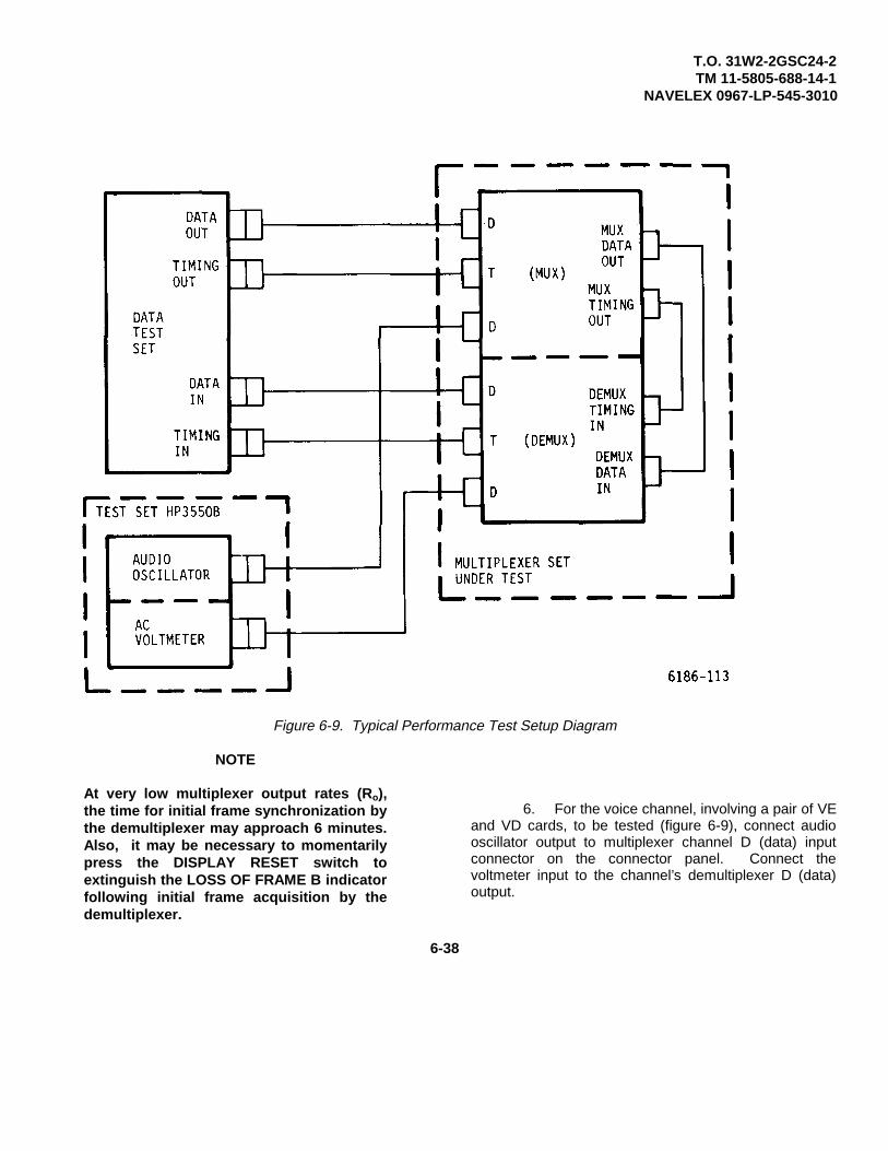
T.O. 31W2-2GSC24-2TM 11-5805-688-14-1
NAVELEX 0967-LP-545-3010
Figure 6-9. Typical Performance Test Setup Diagram
NOTE
At very low multiplexer output rates (Ro),the time for initial frame synchronization bythe demultiplexer may approach 6 minutes.Also, it may be necessary to momentarilypress the DISPLAY RESET switch toextinguish the LOSS OF FRAME B indicatorfollowing initial frame acquisition by thedemultiplexer.
6. For the voice channel, involving a pair of VEand VD cards, to be tested (figure 6-9), connect audiooscillator output to multiplexer channel D (data) inputconnector on the connector panel. Connect thevoltmeter input to the channel’s demultiplexer D (data)output.
6-38

T.O. 31W2-2GSC24-2TM 11-5805-688-14-1
NAVELEX 0967-LP-545-3010
Figure 6-10. Test Setup Cable Diagram
6-39

T.O. 31W2-2GSC24-2TM 11-5805-688-14-1
NAVELEX 0967-LP-545-3010
NOTE
The audio oscillator and voltmeter used inthe following procedures are Hewlett-Packard Models 204C (option 25) and 403B(option 001), respectively, configured aspart of the Hewlett-Packard Model 3550Bportable test set. Equivalent items may besubstituted. Voice channel input/outputimpedance is 600 ohms (balanced).
7. Set audio oscillator output frequency to1000 Hz +5 percent.
8. Set audio oscillator output level to -16 +0.1dBm.
9. Measure audio voltage amplitude appearingat the channel’s demultiplexer output. Amplitude shouldbe +7 +0.1 dBm.
10. Repeat steps 6 through 9 for each voicechannel being tested.
11. Set POWER CONTROL switch to OFF anddisconnect all test setup cables.
6-42. BIT COUNT INTEGRITY TEST. Perform digitalchannel bit count integrity (BCI) test as follows:
NOTE
Testing of the BCI requires that themultiplexer set be set up in a full duplexconfiguration. Refer to chapter 3 for setupinstructions.
1. Connect cables between multiplexer MUXDATA OUT and demultiplexer DEMUX DATA INconnectors, and between multiplexer MUX TIMING OUTand demultiplexer DEMUX TIMING IN connectors (figure6-9).
NOTE
Cable requirements are identified in figure6-10.
2. If testing is performed in a shop area,connect multiplexer set to a source meeting the powerrequirements specified in table 1-1.
3. Set POWER CONTROL switch to ON.
4. Momentarily press DISPLAY RESETswitch.
5. Observe that POWER CONTROL ONindicator is lighted and the following indicators are out:
LOSS OF MUX TIMING
LOSS OF DEMUX TIMING
LOSS OF FRAME A
LOSS OF FRAME B
LINK ERROR RATE
POWER SUPPLY
TEMPERATURE
MULTIPLEXER CARD
DEMULTIPLEXER CARD
NOTE
ì At very low multiplexer output rates(Ro), the time for initial framesynchronization by the demultiplexermay approach 6 minutes. Also, it maybe necessary to momentarily press theDISPLAY RESET switch to extinguishthe LOSS OF FRAME B indicatorfollowing initial frame acquisition by thedemultiplexer.
6-40

T.O. 31W2-2GSC24-2TM 11-5805-688-14-1
NAVELEX 0967-LP-545-3010
• If the digital channel being tested isconfigured with a TE/TR card, the timingcable is not required. Cablerequirements are identified in figure 6-10.
ì The Harris Model 7003 DigitalCommunications Test Set or any otherequivalent data test set that is availablemay be used for digital channel BCItesting. The selected data test set mustsatisfy the multiplexer input/outputinterface requirements specified in table1-3, provide pseudorandom datapatterns of 23-1 or greater bits in length,and be capable of injecting anddetecting data bit errors. Proper test setoperation without a timing inputaccompanying the digital data streambeing monitored is also required.
6. For the digital data channel to be tested,connect timing and data cables between the data test setoutput and the appropriate channel T (timing) and D(data) multiplexer inputs. Connect timing and datacables between the channel’s demultiplexer T (timing)and D (data) outputs and the data test set input (figure 6-9).
7. Set data test set output for an error-freepseudorandom data pattern of 23-1 or greater bits inlength.
8. Set data test set output rate to within +5parts per million (ppm) of the channel’s designated inputrate (Rc).
9. Initiate pseudorandom data pattern andobserve that no data bit errors are detected during aperiod of approximately 1 minute.
10. Set data test set to inject one or moreerrors in its output data pattern and observe that acorresponding number of errors is measured at the datatest set input.
11 Set data test set for an error-free output.
12. If the channel under test is being processedusing a multiplexer RCB channel card, set data test setoutput rate to a value approximately 2500 ppm greaterthan the channel’s designated input rate (Ro). If a TE/TRcard is used, proceed to step 15.
13. Observe that front panel MULTIPLEXEROUT OF TOL indicator lights and the number of thechannel under test appears in FAULT LOCATIONdisplay.
NOTE
There may be several seconds of delaybefore the MULTIPLEXER OUT OF TOLindicator goes out when step 14 isperformed.
14. Repeat step 8 and observe thatMULTIPLEXER OUT OF TOL indicator goes out and thenumber of the channel under test disappears fromFAULT LOCATION display.
15. Repeat steps 6 through 14 for each digitalchannel being tested.
16. Set POWER CONTROL switch to OFF anddisconnect all test setup cables.
6-41

T.O. 31’W2-2GSC24-2TM 11-5805-688-14-1
NAVELEX 0967-LP-545-3010SECTION II
SPECIAL MAINTENANCE
6-43. INTRODUCTION.
6-44. This section provides instructions and dataapplicable to special and depot maintenance of themultiplexer set. Included are procedures for repair ofbackplane assembly connectors, and semipermanentlymounted chassis mechanical parts. Repair of the powersupply and the plug-in cards is performed at a depotfacility as prescribed in paragraph 6-48.
6-45. Aside from certain specific areas discussed inthis section, special maintenance practices performed onthe multiplexer set are consistent with those applicable toother military electronic equipment. Personnelperforming special maintenance should have a highdegree of familarity with these practices, as well as athorough understanding of the multiplexer set theory ofoperation.
6-46. GENERAL.
6-47. Repair of the multiplexer set at the specialmaintenance level generally entails correction of thosemalfunctions that are beyond the scope of theorganizational and intermediate levels. The tasksinclude repair of the structural components and electricalconnectors in the multiplexer set.
6-48. The testing, troubleshooting, and repair of the 12plug-in cards and the power supply are performed at adepot facility. The detailed procedures are contained in
supplemental manual T.O. 31W2-2GSC24-2-1 which isauthorized for depot use only. The detailed instructionsfor removing and installing the plug-in cards and thepower supply are contained in section I of this manual.
6-49. MAINTENANCE SUPPORT EQUIPMENT.
6-50. Table 6-6 lists tools and test equipment requiredin support of the multiplexer set at the specialmaintenance level. Brief summaries of pertinentperformance characteristics are also provided. Specialmaintenance support equipment items that are also usedat the organizational/intermediate maintenance levels arelisted and described in table 6-1. The items listed intable 6-6 are preferred for multiplexer set specialmaintenance. Items having equivalent (or greater)functional capabilities, however, may be substitutedwhen necessary.
6-51 THROUGH 6-64. DELETED.
6-65. CONNECTOR REPAIR.
6-66. Except for the connectors forming a part of thebackplane wiring assembly, the connectors usedthroughout the multiplexer set are conventional typescommon in most military electronic equipment.Connectors not associated
Change 2 6-42

T.O. 31W2-2GSC24-2TM 11-5805-688-14-1
NAVELEX 0967-LP-545-3010
Table 6-6. Depot/Special Level Support Equipment (Equivalent equipment is authorized.)
National Stock No./Item Part No. Pertinent Characteristics
Chassis repair kit,consisting of:
Dolly ESNA P/N CDFB6
Dolly ESNA P/N CDFB8
Hand insertion tool Sealectro P/N HT-1
Handle ESNA P/N CHM1
Handle ESNA P/N CHM2
Handle Kaynar P/N KT7200
Insertion tool Sealectro P/N B22
Installation tool 5120-00-169-3003
Installation tool Southco P/N 29-47-101-10
Punch ESNA P/N CPFA6
Punch ESNA P/N CPFA10
Squeeze tool Kaynar P/N KT7202-046
Squeeze tool Kaynar P/N KT7202-083
Connector repair kit, Martin Marietta P/Nconsisting of: SK63759367
Crimp tool 5120-00-042-7076
Crimp tool 5120-00-897-0188
Extraction tool 5120-00-963-7661
Extraction tool ITT Cannon P/N CET-DL-2
Extraction tool ITT Cannon P/N CET-12-14
Change 2 6-43

T.O. 31W2-2GSC24-2TM 11-5805-688-14-1
NAVELEX 0967-LP-545-3010
Table 6-6. Depot/Special Level Support Equipment (Cont)
National Stock No./Item Part No. Pertinent Characteristics
Hand crimp tool ITT Cannon P/N CCT-DLInsertion/extration 5120-00-230-3770
toolDigital multimeter: 6625-00-188-3892 a. Measures dc voltages
Hewlett-Packard Model between 0 and +25 vdc3490A at accuracy of 0.1%.
b. Measure ac voltages between 0 and 125 vac+0.4%.
Distortion Analyzer: ---- Measures signal-to-noiseHewlett-Packard ratio greater than -26Model 331A dBm below signal level.
Frequency counter: 6625-992-3586 Measures frequency rangeHewlett-Packard between 0-50 x 106 Hz.Model 5245M Accuracy of 1 count, + time base accuracy.
Sensitivity is 100 mv rms.
Function generator: 6625-00-466-0586 Generates 38.4 kHz +3%Hewlett-Packard square wave at 3.0Model 3310A +0.lv p/p.
Insulation resistance 6625-00-160-1131 Measures insulationmeter: Hewlett- resistance of 10 megohmsPackard Model 4329A minimum at 200 vdc.
Multimeter: Triplett 6625-553-0251 a. Measures dc voltagesModel 630A between 0 and 6000 vdc at accuracy of +1.5%.
b. Measures ac voltages between 0 and 6000vac +3.0%.
Oscilloscope main frame: 6625-00-115-2402 Provides visual displayTektronix Model R7704A with a vertical bandpasswith: of 150 mHz, with a riseProbe: Model P6063A time of 2.0 ns.Time base: Model 7B92Dual vertical
amplifier: Model7A26
Power supply: 6625-00-437-4861 Supplies 0 to +15 vdc atHewlett-Packard 0.5 ampere.Model 6205B
Change 2 6-44

T.O. 31W2-2GSC24-2TM 11-5805-688-14-1
NAVELEX 0967-LP-545-3010Table 6-6. Depot/Special Level Support Equipment (Cont)
National Stock No./Item Part No. Pertinent Characteristics
Power supply test set 6625-01-012-8779 Item peculiar to the multi-Martin Marietta P/N plexer set power supply.61868300-009
Signal generator: 6625-00-489-3732 a. Generates audio fre-Hewlett-Packard quency of 1 kHz +5%Model 204D at -16 +0.1 dBm.
b. Output impedance of 600 ohms (balanced).
Subassembly test set Item peculiar to multi-Martin Marietta P/N plexer printed circuit61868000-009 cards.
Transmission and Noise 6625-00-255-1083 Measures 1 kHz signals withMeter: Hewlett- signal levels of -46Packard Model 3555B +0.2 dBm. Also, noise levels of -48 dBm.
Voltmeter: Hewlett- 6625-00-727-4706 Measures audio voltage ofPackard Model 3400A +7 +0.1 dBm at frequency of 1 kHz +5%.
Wattmeter: Weston Weston P/N 432-9902005 a. Measures power levelsModel 432 between 0 and 1500watts +0.5%.
b. Operates on single-phase inputs of up to200 vac.
Pages 6-46 through 6-48, including figures 6-11 through 6-13, deleted.
Change 2 6-45

T.O. 31W2-2GSC24-2TM 11-5805-688-14-1
NAVELEX 0967-LP-545-3010
with the backplane wiring assembly are repaired inaccordance with existing depot and special maintenanceactivity practices. The tools used for such repair areincluded in the connector repair tool set listed in table 6-6.
6-67. Repair card receptacle connectors located onthe backplane wiring assembly by replacing individualcontacts as follows:
NOTEIn the following procedures, it is assumedthat the backplane wiring assembly hasbeen previously removed from themultiplexer set chassis as prescribed inparagraph 6-76.
1. Select a flat clean work surface, preferablyof metal.
2. Position backplane assembly with affectedconnector supported above work surface on square orrectangular metal bars and with contact tails facingupward as shown in figure 6-14. Use bars whosedimensions will allow a minimum clearance of 1 inchbetween connector and work surface.
3 Position a small nail set or other tool with acupped point vertically over tail of connector pin beingreplaced (figure 6-14).
4. Tap nail set with a mediumweight hammeruntil contact falls free or, in the case of a power orground contact, until contact is loosened from itsnormally installed position.
5. If the contact is retained by a groundbushing in the backplane or voltage bus bar, grasp thetail end of contact with needle-nose pliers and pushcontact until its engaging end emerges from connectorinsulator. Then grasp engaging end of contact with the
pliers and pull contact from connector.
NOTE
Replacement contacts have slightly largerbarbs than the original contacts. The largerbarbs compensate for material removedfrom the insulator cavity during removal ofthe original contact. The part number ofthe replacement contact is 030-7311-003.
6. Insert replacement contact tail first intoinsulator cavity from the engaging side of insulator untilcontact bottoms in cavity.
When installing a contact, ensure that theholding pressure exerted on the pliers issufficient to hold the contact securely. Ifthe jaws of the pliers are allowed to slip onthe surface of the contact, removal ofcontact plating may occur.
7. Using needle-nose pliers, grasp tail ofcontact near its end and pull contact until it is properlylocated within the insulator. The contact will be felt tosnap into place when it is fully seated within the insulatorcavity.
6-68. CHASSIS REPAIR.
6-69. GENERAL. The multiplexer set chassis isequipped with items such as captive screws, feed-thruterminals, and clinch nuts, which are installed in asemipermanent manner. Although these items are notintended to be replaced frequently, damage resultingfrom abnormal transportation, operation, or maintenancepractices may necessitate their replacement.
Change 2 6-49/(6-50 blank)

T.O. 31W2-2GSC24-2TM 11-5805-688-14-1
NAVELEX 0967-LP-545-3010
Figure 6-14. Backplane Connector Repair Diagram
The following paragraphs present replacementprocedures for semipermanently mounted chassis parts.
6-70. CAPTIVE SCREW REPLACEMENT.
6-71. Captive retaining screws are provided as part ofthe printed circuit card access cover, the power supplyaccess cover, and the cooling blower panel. Replace
captive retaining screws as follows:
1. Place knurled heat of fastener beingreplaced between opened jaws of a bench vise as shownin figure 6-15.
2. Using a center punch, carefully drive screwportion of fastener
6-51

T.O. 31W2-2GSC24-2TM 11-5805-688-14-1
NAVELEX 0967-LP-545-3010
Figure 6-15. Captive Screw Removal Diagram
from access cover. Remove cover from vise.
3. Grasp remaining portion of fastener withslip-joint pliers, and gently rock fastener back and forthuntil it is released from access cover.
4. Insert replacement fastener through accesscover hole (figure 6-16, view B).
5. Draw knob of installation tool P/N 29-47-101-10 (figure 6-16, view A) to open position, andposition nose of tool against threaded end of fastener(figure 6-16, view B).
6. Return knob of installation tool to closedposition, causing tool to thread onto screw.
7. Lightly squeeze installation tool lever,causing fastener ferrule to flare into countersink inaccess cover.
8. Draw installation tool knob to open position,causing tool to unthread from installed fastener. Aproperly installed fastener is shown in figure 6-16, view C
6-72. Replace captive retaining screws attached to thepower supply heat sink (figure 6-3) as follows:
1. Place power supply, heat sink down, on aworkbench or other suitable flat surface.
2. In a manner similar to that shown in figure6-15, carefully drive center portion of retaining screwfrom heat sink.
6-52

T.O. 31W2-2GSC24-2TM 11-5805-688-14-1
NAVELEX 0967-LP-545-3010
Figure 6-16. Access Cover Captive Screw Insertion Diagram
6-53

T.O. 31W2-2GSC24-2TM 11-5805-688-14-1
NAVELEX 0967-LP-545-3010
3. Turn power supply so that heat sink facesup and grasp remaining portion of captive screw withslip-joint pliers.
4. Gently rock remaining portion of captivescrew back and forth until it is released from heat sink.
5. Turn power supply on its side and insertreplacement captive screw through heat sink hole.
6. Turn threaded portion of screw intoinstallation tool P/N H7503-10 (figure 6-17, view A) byrotating either the screw or the installation tool.
7. Firmly squeeze installation tool handle,causing end of screw ferrule to be swaged against heatsink surface.
8. Unscrew installation tool from installedcaptive screw. Figure 6-17, view B, shows a captivescrew before and after installation
6-73. DELETED.
6-74. STAKE NUT REPLACEMENT. Stake nuts areused within the multiplexer set chassis for purposes ofreceiving the captive screws that secure the access
covers and panel assemblies. Replace stake nuts asfollows:
1. Select a drift or pin punch whose diameterwill allow it to pass through chassis hole and rest onportion of stake nut swaged into chassis (figure 6-21).
2. Carefully drive stake nut from chassis.
3. Insert replacement nut into chassis hole.
NOTE
Squeeze tool P/N KT7202-046 is used forinstalling size 6-32 stake nuts, and squeezetool P/N KT7202-083 is used for installingstake nuts size 8-32 and 10-32 (figure 6-22,view A).
4. Using appropriate size squeeze tool andhandle P/N KT7200, carefully drive replacement stakenut into chassis until lands of nut are flush with chassissurface as shown in figure 6-22, view B.
6-75. DELETED.
Pages 6-55 through 6-58, including figures 6-17 through 6-20, deleted.
Change 2 6-54

T.O. 31W2-2GSC24-2TM 11-5805-688-14-1
NAVELEX 0967-LP-545-3010
Figure 6-21. Stake Nut Removal Diagram
6-76. BACKPLANE CONNECTOR PANEL REMOVALAND INSTALLATION. To remove a backplaneconnector panel, perform the procedures in steps 1through 9. Perform steps 10 through 12 to install areplacement panel in a chassis. Attaching hardwarelocations are shown in figure 6-25.
1. Remove printed circuit card access cover(figure 6-2) and printed circuit cards from card file asprescribed in steps1 through 4 in paragraph 6-22. Whencards are in card file and the cards are to be placed inthe replacement card file, label each card with the properslot assignment from which the card was removed fromthe card file to ensure that cards are placed in proper
slots.
2. Inside the card file, remove four screws(figure 6-25) securing bottom of card file to chassis, fourscrews securing top of card file to chassis, and 10screws securing left side of card file to chassis.
3. Remove rear connector panel anddisconnect cable assemblies as prescribed in paragraph6-28.
4 On rear of card file assembly, remove fourscrews on left side of chassis frame securing card fileassembly to chassis.
6-59

T.O. 31W2-2GSC24-2TM 11-5805-688-14-1
NAVELEX 0967-LP-545-3010
Figure 6-22. Stake Nut Insertion Diagram
6-60

T.O. 31W2-2GSC24-2TM 11-5805-688-14-1
NAVELEX 0967-LP-545-3010
Figure 6-23. DELETED.Figure 6-24. DELETED.
On right side of chassis frame, remove four screwssecuring card file assembly to chassis.
5. Disconnect power cables from terminalsE1, E2, E3, and E4 on backplane panel.
When performing steps 6 and 7, use care toprevent damage or wire breakage of finewiring on rear of card file.
6. Remove four screws securing capacitorassembly on bottom rear of backplane connector panelto chassis.
When performing step 7, insure thatcapacitor assembly on rear of backplaneconnector panel is not subjected to anypressure that could cause damage to theassembly on backplane wiring.
7. Slide card file assembly forward in chassisand then lift from chassis.
Change 2 6-61/(6-62 blank)

T.O. 31W2-2GSC24-2TM 11-5805-688-14-1
NAVELEX 0967-LP-545-3010
Figure 6-25. Card File - Mounting Hardware Location Diagram
6-63

T.O. 31W2-2GSC24-2TM 11-5805-688-14-1
NAVELEX 0967-LP-545-3010
NOTE
Perform steps 8 and 9 to remove and installbackplane connector panel on rear of cardfile. Proceed to step 10 to installreplacement card file in chassis whenbackplane connector panel is not removedfrom card file.
8. Remove 12 screws securing backplaneconnector panel to card file. Remove panel from cardfile.
9. Install replacement backplane connectorpanel to rear of card file. Secure panel to card file, using12 screws removed in step 8
When performing step 10, insure thatcapacitor assembly on rear of backplaneconnector panel is not subjected to anypressure that could cause damage to theassembly or backplane wiring.
10. To install replacement or repairedbackplane connector panel mounted in the card file
assembly, slide rear of card file assembly into chassis,and position card file to attach mounting prescribed instep 11.
11. Mount card file to chassis, using screwsremoved in steps 2 and 4. Install screws removed in step6 to secure capacitor assembly on rear of backplaneconnector panel to chassis.
Torque nuts on E1 through E4 on backplane panel down as prescribed in step 12.Otherwise, intermittent operation ofequipment may occur.
12. Torque lower level nuts on E1 and E2between 70 and 75-inch-pounds. Torque lower level nutson E3 and E4 between 16 and 18 inch-pounds. Installcable terminals on E1 through E4 that were removed instep 5. Then torque upper level nuts on E1 and E2between 70 and 75 inch-pounds. Torque upper levelnuts on E3 and E4 between 16 and 18 inch-pounds.
13. Install rear connector panel and cableassemblies that were removed in step 3 as prescribed inparagraph 6-28.
SECTION III
PERFORMANCE TEST CHECKS
6-77. Multiplexer set performance test checks areapplicable to individual power supply assemblies andprinted circuit cards and to the overall multiplexer set.
6-78. The performance test checks applicable to thepower supply and printed circuit cards are insupplemental manual F.O. 31W2-2GSC24-2-1.
6-79 The performance test checks applicable to theoverall multiplexer set include self-testing, lamp testing,voice processing performance tests, and digital channelbit count integrity (BCI) tests. The procedures for thesetests are contained in paragraphs 6-32, 6-33, 6-41, and6-42, respectively.
Change 2 6-64

T.O. 31W2-2GSC24-2TM 11-5805-688-14-1
NAVELEX 0967-LP-545-3010
A
ASYNCHRONOUS - Signals or events which are not synchronous or not of a common period and phase (frequency) relationship one to another.
B
BIT COUNT INTEGRITY - (BCI) - A measure of the multiplexer set’s ability to process applied channel data without inducing data errors.
C
CHANNEL - A single subscriber’s interface with the multiplexer set.
CHANNEL CARD - See MULTIPLEXER CHANNELCARD and DEMULTIPLEXER CHANNEL CARD.
CHANNEL DATA RATE - (Rc) - The rate at which channel data enter the multiplexer or leave the demultiplexer.
CHANNEL DATA SAMPLING RATE - (KRp) The product of the port sampling (Rp) rate and the number (K) of ports assigned to the channel.
COMMON CARD See - MULTIPLEXER COMMON CARD and DEMULTIPLEXER COMMON CARD.
D
DATA SAMPLING RATE See CHANNEL-DATA SAMPLING RATE.
DATA WORD - One multiplexer port scan containing one bit from each used port plus one bit from theoverhead port. Maximum length of a data word is 32 bits; the minimum length is 16 bits.
DEMULTIPLEXER CHANNEL CARD - One of four
functional printed circuit cards that receives one demultiplexed data channel and processes the data (with or without timing) into the original formin which it was applied to the far end multiplexer.
DEMULTIPLEXER COMMON CARD - One of the five functional printed circuit cards that perform the demultiplexing of the high-speed serial data input stream into the original channel data inputsthat are applied to the demultiplexer channel cards.
DIAGNOSTIC CIRCUITS - The multiplexer, demultiplexer, and power supply circuits that detect and signal the occurance of faulty functional circuit operation.
F
FRAME SYNCHRONIZATION - Synchronization of the bit and word format intervals of receiving demultiplexer with those of the transmitting multiplexer.
FUNCTIONAL CIRCUITS - Multiplexer and demultiplexer circuits other than the diagnostic circuits.
MMAJOR FRAME - A major frame contains 31 minor
frames of data. Each minor frame contains channel data, and overhead data pertaining to one of the 31 ports.
MINOR FRAME - A minor frame contains 29 channel data words and overhead data for one port.
MULTIPLEXER CHANNEL CARD One of three functional printed circuit cards that performs the input function of converting incoming asynchronous data for one channel into a synchronous form that is subsequently applied to
the multiplexer common cards for multiplexing.
Glossary 1

T.O. 31W2-2GSC24-2TM 11-5805-688-14-1
NAVELEX 0967-LP-545-3010
MULTIPLEXER COMMON - CARD One of four functional printed circuit cards that perform the timing functions associated with multiplexing associated channel data inputs of the channel cards into high-speed data output stream.
MULTIPLEXER OUTPUT RATE (R, ) The rate at which multiplexed channel and overhead data leave the multiplexer. Maximum value of Ro is 10 MBPS.
N
NEGATIVE STUFF - Overhead function performed in themultiplexer to compensate for a channel data rate (Rc) isless than the multiplexer channel sampling rate (KRP).
NO ACTION - Overhead function performed in the multiplexer when the channel data rate (Rc) is equal to the multiplexer channel sampling rate (KRp).
0
OVERHEAD DATA - See OVERHEAD MESSAGE FORMAT.
OVERHEAD MESSAGE FORMAT - The overhead message format consists of one 29bit overhead word. One bit of this word occupies bit zero of the 29 data words in each minor frame.
OUTPUT RATE See MULTIPLEXER OUTPUT RATE.
OVERHEAD WORD See - OVERHEAD MESSAGE FORMAT.
P
PORT - An interval of time during which data from a particular channel are allowed into the outputstream in the multiplexer. There are 31 ports
available for use by the 1 to 15 channels in a given system application.
PORT SAMPLING RATE - (Rp) The nominal rate at which the porting occurs. See CHANNEL SAMPLING RATE.
PORT STRAPPING - (K) The number of ports assigned to each input/output channel. Value of K is an integer between 1 and 25. See CHANNEL SAMPLING RATE.
POSITIVE STUFF - Overhead function performed in the multiplexer to compensate for a channel data rate (Rc) that is greater than the multiplexer channel sampling rate (KRp).
STANDARD ERROR ENVIRONMENT - A random error environment of, on the average, one error per hundred bits.
STUFFING - See NEGATIVE STUFF, POSITIVE STUFF, and NO ACTION.
SYNCHRONOUS - Signals or events happening at the same time or having the same period and phaserelationship.
SYSTEM CLOCK RATE - The multiplexer internal master timing rate (MRIO or DRIO) equal to the multiplexer output rate (Ro).
T
TANDEMING - The function of inputting one multiplexer with the output of another multiplexer.
U
USED PORT A port that is assigned to a channel.
Glossary 2

T.O. 31W2 - 2GSC24 - 2TM 11-5805-688-14-1
NAVELEX 0967-LP-545-3010
CROSS-REFERENCE INDEX
A
AN/GSC-24(V) Multiplexer Set(See Multiplexer Set)
B
Backplane WiringInstallation, Connector Panel. ................................................................................................................... 6-76Removal, Connector Panel ....................................................................................................................... 6-76Repair ....................................................................................................................................................... 6-28
F6-5F6-6F6-14
C
Card FileMounting Hardware Location......................................................................................................................... F6-25Removal and Replacement. ............................................................................................................................ 6-76
Cooling Air BlowerAir Filter Cleaning. .................................................................................................................................... 6-36Air Filter Replacement. ............................................................................................................................. 6-27Functional Operation................................................................................................................................. 5-618
DDemultiplexer
Basic Concepts ......................................................................................................................................... 5-55Block Diagram Discussion ........................................................................................................................ 5-106
FO-2Channel Card Setup Procedures. ................................................................................................................... 3-78Common Card Setup Procedures ................................................................................................................... 3-84
Display CardBlock Diagram F5-43
F5-44Functional Operation................................................................................................................................. 5-563Repair and Replacement .......................................................................................................................... 6-21
6-22Setup Procedures ..................................................................................................................................... 3-91Switch Location Diagram................... ..................................................................................................... F3-22
Display Circuit Card Assembly(See Display Card)
CRI-1

T.O. 31W2-2GSC24-2TM 11-5805-688-14-1
NAVELEX 0967-LP-545-3010
EERD Card
Block Diagrams....................................................................................................................................... F5-40F5-41F5-42FO-10
Functional Operation................................................................................................................................. 5-535Repair and Replacement .......................................................................................................................... 6-21
6-22Setup Procedures ..................................................................................................................................... 3-90Switch Location Diagram ........................................................................................................................ F3-21
Error Rate Detector and Remote Alarms Circuit Card Assembly(See ERD Card)
Extender Card Usage...................................................................................................................................... 6-17
F
Fan(See Cooling Air Blower)
Frame Sync Circuit Card Assembly(See FS Card)
Front PanelBlock Diagram Discussion ........................................................................................................................ 5-154Controls and Indicators. ............................................................................................................................ 4-3
F4-1T4-1
Detailed Circuit Discussion ....................................................................................................................... 5-612Indicator Lamp Replacement .................................................................................................................... 6-25LED Element Replacement ...................................................................................................................... 6-26Operating Instructions............................................................................................................................... 4-5Printed Circuit Card Jumper Location Diagram ...................................................................................... F3-23Repair. ...................................................................................................................................................... 6-21Replacement............................................................................................................................................. 6-24
FS CardBlock Diagrams....................................................................................................................................... F5-36 to
F5-39FO-6 toFO-9
Functional Operation................................................................................................................................. 5-472Repair and Replacement .......................................................................................................................... 6-21
6-22Setup Procedures ..................................................................................................................................... 3-89Switch Location Diagram. ....................................................................................................................... F3-20
CRI-2

T.O. 31W2-2GSC24-2TM 11-5805-688-14-1
NAVELEX 0967-LP-545-3010
G
Gated Clock/Data Mux Circuit Card Assembly(See GC/DM Card)
GC/DM CardBlock Diagrams....................................................................................................................................... F5-22 to
F5-26Functional Operation (Demux).................................................................................................................. 5-463Functional Operation (Mux) ...................................................................................................................... 5-306Repair and Replacement .......................................................................................................................... 6-21
6-22Setup Procedures (Demux)............................................................................................................................. 3-88Setup Procedures (Mux) ................................................................................................................................. 3-77
M
MultiplexerBasic Concepts. ........................................................................................................................................ 5-19Block Diagram Discussion ........................................................................................................................ 5-69
FO-1Channel Card Setup Procedures. ............................................................................................................. 3-66Common Card Setup Procedures............................................................................................................. 3-72
Multiplexer SetApplication ................................................................................................................................................ 3-5
5-27Built-In Diagnostic Features...................................................................................................................... 6-8Capabilities, Unique.................................................................................................................................. 1-3Channel Card Options .............................................................................................................................. 3-27
T3-1T3-1
Controls and Indicators. ............................................................................................................................ 4-3T4-1
Description.. .............................................................................................................................................. 1-1Diagnostic Self-Testing ............................................................................................................................. 6-32Electrical Capabilities and Limitations....................................................................................................... 1-8
T1-3Equipment Supplied.................................................................................................................................. 1-10
T1-4Leading Particulars. .................................................................................................................................. 1-6
T1-1Maintenance 6-5
6-47Operational Tests...................................................................................................................................... 3-97Overhead Service ..................................................................................................................................... 5-48
F5-7Physical Arrangement............................................................................................................................. F6-2Physical Capabilities and Limitations........................................................................................................ 1-8
T1-2Physical View.......................................................................................................................................... F1-1Power Supply, Physical View.................................................................................................................. F1-4Printed Circuit Card, Location View ........................................................................................................ F1-2
CRI-3

T.O. 31W2-2GSC24-2TM 11-5805-688-14-1
NAVELEX 0967-LP-545-3010
Purpose... ........................................................................................................................................................ 1-1Typical Duplex Configurations......................................................................................................................... 3-8
F3-1Typical Multiplexer Application ...................................................................................................................... F5-3Typical Printed Circuit Board......................................................................................................................... F1-3Typical Simplex Configuration......................................................................................................................... 3-9
F3-2N
Narrow Band Smoothing Buffer Circuit Card Assembly(See NBSB Card)
NBSB CardFunctional Operation................................................................................................................................. 5-419Repair and Replacement .......................................................................................................................... 6-21
6-22Setup Procedures 3-81Switch Location Diagram ........................................................................................................................ F3-18
OOEG Card
Block Diagram ........................................................................................................................................ F5-27Functional Operation (Demux).................................................................................................................. 5-468Functional Operation (Mux) ...................................................................................................................... 5-351Repair and Replacement .......................................................................................................................... 6-21
6-22Setup Procedures (Demux) ...................................................................................................................... 3-86Setup Procedures (Mux ............................................................................................................................ 3-75Switch Location Diagram ........................................................................................................................ F3-15
Overhead Enable Generator Circuit Card Assembly(See OEG Card)
P
Power Supply (Assembly)Assembly (Deleted)Assembly Views (Deleted)
F6-11F6-12
Block Diagram. .............................................................................................................................................. F0-11Functional Operation .........................................................................................................................................5-620Maintenance Concept........................................................................................................................................6-5Physical View................................................................................................................................................. F1-4Repair (Deleted)Replacement.......... ......................................................................................................................................... 6-23Test Setup Diagram (Deleted)Testing/Troubleshooting (Deleted)
Change 2 CRI-4

T.O. 31W2-2GSC24-2TM 11-5805-688-14-1
NAVELEX 0967-LP-545-3010R
Rate Comparison Buffer Circuit Card Assembly(See RCB Card)
RCB CardBlock Diagrams ............................................................................................................................................. F5-11
F5-12F5-13F5-14
Functional Operation................................................................................................................................. 5-166Repair and Replacement .......................................................................................................................... 6-21
6-22Setup Procedures ..................................................................................................................................... 3-68Switch Location Diagram.. F3-12
Receiving Data.... ............................................................................................................................................ 2-7
Reference Timer Circuit Card Assembly(See RT Card)
RT CardBlock Diagrams....................................................................................................................................... F5-28
F5-29F5-30
Calibration................................................................................................................................................. 6-34F6-8
Functional Operation................................................................................................................................. 5-373Repair and Replacement .......................................................................................................................... 6-21
6-22Setup Procedures. .................................................................................................................................... 3-74Switch Location Diagram. ....................................................................................................................... F3-14
SSB Card
Block Diagrams....................................................................................................................................... F5-32FO-4
Functional Operation................................................................................................................................. 5-396Repair and Replacement .......................................................................................................................... 6-21
6-22Setup Procedures ..................................................................................................................................... 3-80Switch Location Diagram ........................................................................................................................ F3-17
Seq CardBlock Diagram ........................................................................................................................................ FO-3Functional Operation (Demux).................................................................................................................. 5-460Functional Operation (Mux) ...................................................................................................................... 5-265
T3-6Repair and Replacement .......................................................................................................................... 6-21
6-22
CRI-5

T.O. 31W2-2GSC24-2TM 11-5805-688-14-1
NAVELEX 0967-LP-545-3010
Setup Procedures (Demux) ..................................................................................................................... 3-87Setup Procedures (Mux) ........................................................................................................................... 3-76Switch Location Diagram ........................................................................................................................ F3-16
Sequencer Circuit Card Assembly(See Seq Card)
Smoothing Buffer Circuit Card Assembly(See SB Card)
T
TD CardBlock Diagrams....................................................................................................................................... F5-33
F5-34FO-5
Functional Operation................................................................................................................................. 5-426Repair and Replacement .......................................................................................................................... 6-21
6-22Setup Procedures ..................................................................................................................................... 3-83Switch Location Diagram ........................................................................................................................ F3-19
TE/TR CardBlock Diagrams....................................................................................................................................... F5-15
F5-16F5-17F5-18F5-19
Calibration................................................................................................................................................. 6-35Functional Operation................................................................................................................................. 5-203Repair and Replacement .......................................................................................................................... 6-21
6-22Setup Procedures ..................................................................................................................................... 3-70Switch Location Diagram ........................................................................................................................ F3-13
Transition Decoder Circuit Card Assembly(See TD Card)
Transition Encoder and Timing Recovery Circuit Card Assembly(See TE/TR Card)
V
VD CardBlock Diagram ........................................................................................................................................ F5-35Functional Operation................................................................................................................................. 5-444Repair and Replacement .......................................................................................................................... 6-21
6-22Setup Procedures ..................................................................................................................................... 3-82
CRI-6

T.O. 31W2-2GSC24-2TM 11-5805-688-14-1
NAVELEX 0967-LP-545-3010VE Card
Block Diagram ........................................................................................................................................ F5-21Functional Operation................................................................................................................................. 5-245Repair and Replacement .......................................................................................................................... 6-21
6-22Setup Procedures ..................................................................................................................................... 3-71
Voice Decoder Circuit Card Assembly(See VD Card)
Voice Encoder Circuit Card Assembly(See VE Card)
CRI-7/CRI-8 blank)

T.O. 31W2-2GSC24-2TM 11-5805-688-14-1
NAVELEX 0967-LP-545-3010
ALPHABETICAL INDEX
A
AC Power Distribution. .................................................................................................................................... 5-516F5-45
Air Filter Cleaning. ........................................................................................................................................... 6-36Alarms, Visual. .............................................................................................................................................. T4-1Analog Phase Lock Loop (APLL) .................................................................................................................... 5-401AN/GSC-24(V) Multiplexer Set
(See Multiplexer Set)Assembly (See Specific Item)Asynchronous-to-Synchronous Conversion .................................................................................................... 5-30
F5-4Automatic Diagnostic Circuits.......................................................................................................................... 1-3
6-10
BBackplane Wiring
Installation, Connector Panel. ................................................................................................................... 6-76Removal, Connector Panel ....................................................................................................................... 6-76Repair ....................................................................................................................................................... 6-28
F6-5F6-6F6-14
Basic Equipment Concept ............................................................................................................................... 5-5Demultiplexer ............................................................................................................................................ 5-55Message Format. ...................................................................................................................................... 5-7Multiplexer................................................................................................................................................. 5-19
Bit Count Integrity Test... ................................................................................................................................. 6-42Broadcast (Simplex) System Configuration..................................................................................................... 3-10
F3-2
C
Captive ScrewInsertion Diagram, Access Cover. .......................................................................................................... F6-16Insertion Diagram, Power Supply................ ........................................................................................... F6-17Removal Diagram ................................................................................................................................... F6-15Replacement............................................................................................................................................. 6-70
Card Extender Usage...................................................................................................................................... 6-17Card File
Mounting Hardware Location. ................................................................................................................. F6-25Removal & Replacement .......................................................................................................................... 6-76
Card Removal and Replacement.. .................................................................................................................. 6-22Card Setup Procedures
(See Specific-Card)Card Types. ..................................................................................................................................................... 1-5Channel and Ports Relationship...................................................................................................................... 3-11
Index 1

T.O. 31W2-2GSC24-2TM 11-5805-688-14-1
NAVELEX 0967-LP-545-3010
Channel Card Options... .................................................................................................................................. 3-27T3-1
Channel Card Setup Procedures(See Specific Card)
Channel Rates and FormsDigital Data With Timing ........................................................................................................................... 3-19Digital Data Without Timing ...................................................................................................................... 3-22Voice Data ................................................................................................................................................ 3-25
Chassis Repair ................................................................................................................................................ 6-68CIRCUIT BREAKER Control ........................................................................................................................... 4-3
T4-1Cleaning Air Filter ............................................................................................................................................ 6-36Clinch Nut Locations on Power Supply (Deleted)Clinch Nut Replacement (Deleted)
Coarse Rate Conversion
Functional Operation................................................................................................................................. 5-181Strapping Data .......................................................................................................................................... 3-69
T3-3Common Cards Setup (See Specific Card)Concepts (See Basic Equipment Concepts)Configuration Considerations, Supplemental. ................................................................................................. 3-45Configuration Worksheet................................................................................................................................. 3-30
T3-2Configuration Worksheets
General ..................................................................................................................................................... 3-29Demultiplexer Channel Electronics. .......................................................................................................... 3-41Demultiplexer Common Electronics.......................................................................................................... 3-43Multiplexer Channel Electronics................................................................................................................ 3-32Multiplexer Common Electronics .............................................................................................................. 3-36Sheet 1 Example..................................................................................................................................... F3-5Sheet 2 Example..................................................................................................................................... F3-6Sheet 3 Example..................................................................................................................................... F3-7Sheet 4 Example..................................................................................................................................... F3-8
Connector Repair..................... ....................................................................................................................... 6-65Continuity Check ............................................................................................................................................. 6-18Controls on Front Panel
(See CIRCUIT BREAKER Control)(See DISPLAY RESET Switch)(See LAMP TEST Switch)(See POWER CONTROL ON/OFF Switch)(See SELF TEST Switch)
Cooling Air BlowerAir Filter Cleaning ..................................................................................................................................... 6-36Air Filter Replacement. ............................................................................................................................. 6-27Functional Operation................................................................................................................................. 5-618
D
Data word Defined........................................................................................................................................... 5-11
Change 2 Index 2

T.O. 31W2-2GSC24-2TM 11-5805-688-14-1
NAVELEX 0967-LP-545-3010Demultiplexer
Basic Concepts ......................................................................................................................................... 5-55Block Diagram Discussion ........................................................................................................................ 5-106
FO-2Demultiplexer Card Indicator
Functional Description .............................................................................................................................. 4-3T4-1
Troubleshooting Aid .................................................................................................................................. 6-8T6-2
Demultiplexer Card Setup ProceduresChannel Cards................ .......................................................................................................................... 3-78Common Cards......................................................................................................................................... 3-84
Depot/Special Maintenance Level SupportEquipment................................................................................................................................................. 6-50
T6-6Description and Purpose (Multiplexer Set)...................................................................................................... 1-1
T1-1Diagnostic Circuit Self-Testing ........................................................................................................................ 6-32Diagnostic Functional Block Diagram
Discussion................................................................................................................................................. 5-138F5-10
Digital DataVoice. ........................................................................................................................................................ 3-25With Timing. .............................................................................................................................................. 3-19Without Timing.......................................................................................................................................... 3-22
Display CardBlock Diagrams....................................................................................................................................... F5-43
F5-44Functional Operation................................................................................................................................. 5-563Setup Procedures ..................................................................................................................................... 3-91Switch Location Diagram. ....................................................................................................................... F3-22
Display Circuit Card Assembly(See Display Card)
DISPLAY RESET Switch/ModeFunctional Description. ............................................................................................................................. 4-3
T4-1Maintenance Testing................................................................................................................................. 6-8
Duplex Configuration....................................................................................................................................... 3-7F3-1
E
Efficiency Configuration ConsiderationsPort Rate Mix Impact. ............................................................................................................................... 3-49
F3-9Input Rate Mix Impact 3-51
F3-10
Electrical Capabilities and Limitations ............................................................................................................. 1-8T1-3
Index 3

T.O. 31W2-2GSC24-2TM 11-5805-688-14-1
NAVELEX 0967-LP-545-3010
Equipment Application..................................................................................................................................... 5-27Equipment Supplied ........................................................................................................................................ 1-10
T1-4ERD CardBlock Diagrams ............................................................................................................................................. F5-40
F5-41F5-42FO-10
Functional Operation................................................................................................................................. 5-535Setup Procedures ..................................................................................................................................... 3-90Switch Location Diagram. ....................................................................................................................... F3-21
Error Rate Detector and Remote AlarmsCircuit Card Assembly(See ERD Card)
Extender Card Usage...................................................................................................................................... 6-17
F
Fan (See Cooling Air Blower)Fault Isolation Modes
Automatic. ................................................................................................................................................. 6-10Lamp Test. ................................................................................................................................................ 6-12
Self-Test......... ................................................................................................................................................. 6-11FAULT LOCATION Numerical Indicator
Functional Description .............................................................................................................................. 4-3T4-1
Troubleshooting Aid .................................................................................................................................. 6-8T6-2
Feed-Thru Terminal Replacement (Deleted)
Frame Sync Circuit Card Assembly(See FS Card)
Frame Synchronization Function..................................................................................................................... 5-57F5-8
Front PanelBlock Diagram Discussion ........................................................................................................................ 5-154Controls and Indicators ............................................................................................................................. 4-3
F4-1T4-1
Detailed Circuit Discussion ....................................................................................................................... 5-612Indicator Lamp Replacement .................................................................................................................... 6-25LED Element Replacement. ..................................................................................................................... 6-26Operating Instructions............................................................................................................................... 4-5Printed Circuit Card Jumper Location Diagram ...................................................................................... F3-23Replacement............................................................................................................................................. 6-24Repair ....................................................................................................................................................... 6-21
FS CardBlock Diagrams....................................................................................................................................... F5-36 to
F5-39FO-6 toFO-9
Functional Operation................................................................................................................................. 5-472
Change 2 Index 4

T.O. 31W2-2GSC24-2TM 11-5805-688-14-1
NAVELEX 0967-LP-545-3010
Setup Procedures ..................................................................................................................................... 3-89Switch Location Diagram ........................................................................................................................ F3-20
Functional OperationDemultiplexer Cards ................................................................................................................................. 5-394Display Card.............................................................................................................................................. 5-563Front Panel ............................................................................................................................................... 5-612Multiplexer Cards ...................................................................................................................................... 5-164Power Supply............................................................................................................................................ 5-620
G
Gated Clock/Data Mux CircuitCard Assembly(See GC/DM Card)
GC/DM CardBlock Diagrams....................................................................................................................................... F5-22 to
F5-26Functional Operation (Demux).................................................................................................................. 5-463Functional Operation (Mux) ...................................................................................................................... 5-306Setup Procedures (Demux) ...................................................................................................................... 3-88Setup Procedures (Mux) ........................................................................................................................... 3-77
H
Homogeneous Sampling Sequence................................................................................................................ 5-46F5-5
Housing RequirementsInstallation................................................................................................................................................. 2-9Storage ..................................................................................................................................................... 2-5
I
Indicators on Front Panel(See DEMULTIPLEXER CARD Indicator)(See FAULT LOCATION Numerical Indicator)(See LINK ERROR RATE Indicator)(See LOSS OF DEMUX TIMING Indicator)(See LOSS OF FRAME A Indicator)(See LOSS OF FRAME B Indicator)(See LOSS OF MUX TIMING Indicator)(See MULTIPLEXER CARD Indicator)(See MULTIPLEXER OUT OF TOLERANCE Indicator)(See POWER CONTROL ON/OFF Indicator)(See POWER SUPPLY Indicator)(See TEMPERATURE Indicator)
Inefficiency of Operation.................................................................................................................................. 3-47Inspection, Visual ............................................................................................................................................ 6-37Installation Data............................................................................................................................................. T2-1Installation Housing Requirements.................................................................................................................. 2-9Installation Procedures.................................................................................................................................... 2-13
Index 5

T.O. 31W2-2GSC24-2TM 11-5805-688-14-1
NAVELEX 0967-LP-545-3010Intermediate Maintenance
(See Organizational/Intermediate Maintenance)
LLAMP TEST Switch/Mode
Functional Description .............................................................................................................................. 4-3T4-1
Maintenance Testing................................................................................................................................. 6-96-126-336-40
Procedures................................................................................................................................................ 4-8Leading Particulars.......................................................................................................................................... 1-6
T1-1LED Element Replacement.......................... ................................................................................................... 6-26
F6-4LINK ERROR RATE Indicator
Functional Description .............................................................................................................................. 4-3T4-1
Troubleshooting Aid ................................................................................................................................ T6-2LOSS OF DEMUX TIMING Indicator
Functional Description .............................................................................................................................. 4-3T4-1
Troubleshooting Aid ................................................................................................................................ T6-2LOSS OF FRAME A Indicator
Functional Description .............................................................................................................................. 4-3T4-1
Troubleshooting Aid ................................................................................................................................ T6-2LOSS OF FRAME B Indicator
Functional Description .............................................................................................................................. 4-3T4-1
Troubleshooting Aid ................................................................................................................................ T6-2LOSS OF MUX TIMING Indicator
Functional Description .............................................................................................................................. 4-3T4-1
Troubleshooting Aid ................................................................................................................................ T6-2
M
Maintenance(See Organizational/Intermediate Maintenance)(See Special Maintenance)
Major Frame Defined....................................................................................................................................... 5-9Message Format ............................................................................................................................................. 5-6
Overall Message Format .......................................................................................................................... 5-7F5-1
Overhead Message Format ...................................................................................................................... 5-13F5-2
Minor Frame Defined....................................................................................................................................... 5-10Multiplexer
Basic Concepts ......................................................................................................................................... 5-19Block Diagram Discussion ........................................................................................................................ 5-69
FO-1
Index 6

T.O. 31W2-2GSC24-2TM 11-5805-688-14-1
NAVELEX 0967-LP-545-3010
MULTIPLEXER CARD IndicatorFunctional Description .............................................................................................................................. 4-3
T4-1Troubleshooting Aid .................................................................................................................................. 6-8
T6-2Multiplexer Card Setup Procedures:
Channel Cards .......................................................................................................................................... 3-66Common Cards......................................................................................................................................... 3-72
MULTIPLEXER OUT OF TOLERANCE IndicatorFunctional Description .............................................................................................................................. 4-3
T4-1Troubleshooting Aid .................................................................................................................................. 6-42
T6-2Multiplexer Set
Application ................................................................................................................................................ 3-55-27
Capabilities, Unique.................................................................................................................................. 1-3Channel Card Options .............................................................................................................................. 3-27
T3-1Controls and Indicators ............................................................................................................................. 4-3
T4-1Description ................................................................................................................................................ 1-1Electrical Capabilities and Limitations....................................................................................................... 1-8
T1-3Equipment Supplied.................................................................................................................................. 1-10
T1-4Leading Particulars ................................................................................................................................... 1-6
T1-1Operational Tests...................................................................................................................................... 3-97Overhead Service ..................................................................................................................................... 5-48
F5-7Physical Arrangement............................................................................................................................. F6-2Physical Capabilities and Limitations........................................................................................................ 1-8
T1-8Physical View.......................................................................................................................................... F-1Power Supply, Physical View.................................................................................................................. F1-4Printed Circuit Card, Location View............ ............................................................................................ F1-2Purpose..................................................................................................................................................... 1-1Typical Duplex Configurations.............. .................................................................................................... 3-8
F3-1Typical Multiplexer Application................................................................................................................ F5-3Typical Printed Circuit Board. ................................................................................................................. F1-3Typical Simplex Configuration .................................................................................................................. 3-9
F3-2
Index 7

T.O. 31W2-2GSC24-2TM 11-5805-688-14-1
NAVELEX 0967-LP-545-3010N
Narrow Band Smoothing BufferCircuit Card Assembly(See NBSB Card)
NBSB CardFunctional Operation................................................................................................................................. 5-419Setup Procedures......... ............................................................................................................................ 3-8
Switch Location Diagram............................................................................................................................... F3-18Negative Stuffing (See Stuffing Function)No Action Stuffing (See Stuffing Function)
O
OEG CardBlock Diagram ........................................................................................................................................ F5-27Functional Operation (Demux. .................................................................................................................. 5-468Functional Operation (Mux) ...................................................................................................................... 5-351Setup Procedures (Demux). ..................................................................................................................... 3-86Setup Procedures (Mux) ........................................................................................................................... 3-75Switch Location Diagram ........................................................................................................................ F3-15
Operating InstructionsControls and Indicators ............................................................................................................................. 4-3Emergency Stopping................................................................................................................................. 4-11Lamp Test ................................................................................................................................................. 4-8Self-Test.................................................................................................................................................... 4-9Starting Procedures .................................................................................................................................. 4-7Stopping Procedures ................................................................................................................................ 4-10
Organizational/Intermediate MaintenanceConcept..................................................................................................................................................... 6-5Fault Isolation with Built-in Diagnostics..................................................................................................... 6-8Inspection.................................................................................................................................................. 6-37Maintenance Support Equipment.............................................................................................................. 6-6
T6-1Paint Touchup........................................................................................................................................... 6-29Performance Standards. ........................................................................................................................... 6-38Preventive Maintenance ........................................................................................................................... 6-30Repair and Replacement .......................................................................................................................... 6-20
Output Message Format(See Message Format)
Output Rate (Ro).............................................................................................................................................. 5-24Overall Message Format ................................................................................................................................. 5-7
F5-1Overhead Data Defined................................................................................................................................... 5-14Overhead Enable Generator Circuit Card Assembly
(See OEG Card)Overhead Message Format............................................................................................................................. 5-13
F5-2Index 8

T.O. 31W2-2GSC24-2TM 11-5805-688-14-1
NAVELEX 0967-LP-545-3010
P
Packaging For Shipment ................................................................................................................................. 3-101Paint Touchup ................................................................................................................................................. 6-29Performance Standards .................................................................................................................................. 6-38Performance Test Checks...... ......................................................................................................................... 6-77Physical Capabilities and Limitations. ............................................................................................................. 1-8
T1-2Port
Definition.. ................................................................................................................................................. 5-21Sampling Sequence.................................................................................................................................. 5-47Number Used in Message Format............................................................................................................ 5-11
Positive Stuffing (See Stuffing Function)Power Cable (Assembly)
Equipment Supplied................................................................................................................................ T1-4Installation................................................................................................................................................. 2-14
F1-1POWER CONTROL ON/OFF Indicator
Functional Description .............................................................................................................................. 4-3T4-1
Troubleshooting Aid. ............................................................................................................................... T6-2POWER CONTROL ON/OFF Switch .............................................................................................................. 4-3
T4-1Power Supply (Assembly)
Assembly (Deleted)Assembly Views...... ...................................................................................................................................... F6-3
Block Diagram. ....................................................................................................................................... FO-11Functional Operation................................................................................................................................. 5-620Maintenance Concept ............................................................................................................................. F6-5Physical View.......................................................................................................................................... F1-4Repair (Deleted)Replacement............................................................................................................................................. 6-23Test Setup Diagram (Deleted)Testing/Troubleshooting (Deleted)
POWER SUPPLY IndicatorFunctional Description..................................................................................................................................... 4-3
T4-1Troubleshooting Aid......................................................................................................................................... 6-8
T6-2Preparation of Configuration Worksheets
(See Configuration Worksheets)Preparing Multiplexer Set for Reshipment....................................................................................................... 3-99Preparing Multiplexer Set for Use
Card Setup Procedures(See Specific Card)Operational Testing................................................................................................................................... 3-97Preparation Considerations ...................................................................................................................... 3-64Thermal Alarm Options ............................................................................................................................. 3-93
Preventive MaintenanceScope........................................................................................................................................................ 6-30
Summary ....................................................................................................................................................... T6-5
Change 2 Index 9

T.O. 31W2-2GSC24-2TM 11-5805-688-14-1
NAVELEX 0967-LP-545-3010Printed Circuit Card
Maintenance Concept ............................................................................................................................... 6-5Repair ....................................................................................................................................................... 6-21
Replacement............................................................................................................................................. 6-22
Testing/Troubleshooting (Deleted)
R
Rate Comparison Buffer CircuitCard Assembly(See RCB Card)
RCB CardBlock Diagrams....................................................................................................................................... F5-11
F5-12F5-13F5-14
Functional Operation................................................................................................................................. 5-166Setup Procedures. .................................................................................................................................... 3-68Switch Location Diagram ........................................................................................................................ F3-12Receiving Data.......................................................................................................................................... 2-7
Reference Timer CircuitCard Assembly(See RT Card)
Related Technical Publications ....................................................................................................................... 1-12T1-5
Repair and ReplacementBackplane Wiring ...................................................................................................................................... 6-28Chassis ..................................................................................................................................................... 6-68Connectors................................................................................................................................................ 6-65Cooling Blower.......................................................................................................................................... 6-27Front Panel Assembly............................................................................................................................... 6-24Front Panel Indicator Lamp....................................................................................................................... 6-25LED Element............................................................................................................................................. 6-26Power Supply............................................................................................................................................ 6-23
6-60Printed Circuit Card................................................................................................................................... 6-22.................................................................................................................................................................. 6-54
Reshipment, Preparation for ........................................................................................................................... 3-99
RT CardBlock Diagrams....................................................................................................................................... F5-28
F5-29F5-30
Calibration................................................................................................................................................. 6-34F6-8
Functional Operation................................................................................................................................. 5-373Setup Procedures ..................................................................................................................................... 3-74Switch Location Diagram ........................................................................................................................ F3-14
Change 2 Index 10

T.O. 31W2-2GSC24-2TM 11-5805-688-14-1
NAVELEX 0967-LP-545-3010S
SB CardBlock Diagrams....................................................................................................................................... F5-32
FO-4Functional Operation................................................................................................................................. 5-396Setup Procedures. .................................................................................................................................... 3-80Switch Location Diagram ........................................................................................................................ F3-17
SELF TEST Switch/ModeFunctional Description. ............................................................................................................................. 4-3
T4-1Maintenance Testing................................................................................................................................. 6-9
6-116-326-40
Procedures................................................................................................................................................ 4-9
Seq CardBlock Diagram ........................................................................................................................................ FO-3Functional Operation (DeMux).................................................................................................................. 5-460Functional Operation (Mux). ..................................................................................................................... 5-265
T3-6Setup Procedures (DeMux) ...................................................................................................................... 3-87Setup Procedures (Mux) ........................................................................................................................... 3-76Switch Location Diagram ........................................................................................................................ F3-16
Sequencer Circuit Card Assembly(See Seq Card)
Setup Procedures(See specific card.)
Signal Names .................................................................................................................................................. 6-15T6-3
Simplex ConfigurationBroadcast Configuration ........................................................................................................................... 3-10
F3-2Typical Configuration ................................................................................................................................ 3-9
F3-2
Smoothing Buffer CircuitCard Assembly(See SB Card)
Smoothing Function .................................................................................................................................. 5-64
Index 11

T.O. 31W2-2GSC24-2’TM 11-5805-688-14-1
NAVELEX 0967-LP-545--010
Special MaintenanceBackplane Connector Panel
Removal and Installation ....................................................................................................................... 6-76Chassis Repair.......................................................................................................................................... 6-68Connector Repair...................................................................................................................................... 6-65Feed-thru Terminal Replacement (Deleted)
Power Supply Repair (Deleted)Power Supply Testing and Troubleshooting (Deleted)Printed Circuit Card Repair (Deleted)Support Equipment ................................................................................................................................... 6-49
T6-6
Special Purpose Switch................................................................................................................................... 6-19T6-4
Special Tools................................................................................................................................................... 1-14T1-6
Stake Nut Replacement .................................................................................................................................. 6-74F6-21F6-22
Starting Procedures......................................................................................................................................... 4-7Stopping ProceduresEmergency ...................................................................................................................................................... 4-11Normal ............................................................................................................................................................. 4-10
Storage Housing Requirement ........................................................................................................................ 2-5
Stuffing FunctionCommand Generation .............................................................................................................................. 5-177Negative Stuff Request. ............................................................................................................................ 5-53No Action Stuff Request............................................................................................................................ 5-51Operation. ................................................................................................................................................. 5-17Overhead Message Format. ..................................................................................................................... 5-13Positive Stuff Request............................................................................................................................... 5-5223-Bit Stuff Code....................................................................................................................................... 5-15
5-17
Supplemental Configuration Considerations. .................................................................................................. 3-45
Switches(See Controls)
Symptoms, Troubleshooting............................................................................................................................ 6-15T6-2
Change 2 Index 12

T.O. 31W2-2GSC24-2TM 11-5805-688-14-1
NAVELEX 0967-LP-545-3010
System ConfigurationsDuplex Description.................................................................................................................................... 3-7Multiplexer Application .............................................................................................................................. 3-5Simplex Description .................................................................................................................................. 3-9
T
TD CardBlock Diagrams....................................................................................................................................... F5-33
F5-34FO-5
Functional Operation................................................................................................................................. 5-426Setup Procedures ..................................................................................................................................... 3-83Switch Location Diagram ........................................................................................................................ F3-19
TE/TR CardBlock Diagrams....................................................................................................................................... F5-15
F5-16F5-17F5-18F5-19
Calibration................................................................................................................................................. 6-35Functional Operation................................................................................................................................. 5-203Setup Procedures.............. ....................................................................................................................... 3-70Switch Location Diagram ........................................................................................................................ F3-13
Technical Manuals, Related. ........................................................................................................................... 1-12T1-5
Temperature IndicatorFunctional Description.. ............................................................................................................................ 4-1
T4-1Troubleshooting Aid....................................................................................................................................... T6-2Test Equipment
Multiplexer Set Maintenance..................................................................................................................... 1-16T1-7
Organizational/Intermediate Maintenance Support Equipment. ............................................................... 6-6Special Maintenance Support Equipment................................................................................................. 6-49
Test Points ................................................................................................................................................ 6-16T6-3
Test ProceduresDiagnostic Self-Test.................................................................................................................................. 6-32Lamp Test ................................................................................................................................................. 6-33Voice Processing Test .............................................................................................................................. 6-41
Theory of OperationDescription ................................................................................................................................................ 5-1(See Functional Operation under specific items.)
Index 13

T.O. 31W2-2GSC24-2TM 11-5805-688-14-1
NAVELEX 0967-LP-545-3010
Thermal Alarm Options. .................................................................................................................................. 3-93
Transition Decoder Circuit Card Assembly(See TD Card)
Transition Encoder and Timing Recovery Circuit Card Assembly(See TE/TR Card)
TroubleshootingAutomatic Mode (Built-In Diagnostics)...................................................................................................... 6-10Continuity Checks.......... ........................................................................................................................... 6-18Special Purpose Switch Usage................................................................................................................. 6-19
T6-4Symptoms ................................................................................................................................................. 6-15
T6-2
Type I Data. ..................................................................................................................................................... 3-20
Type II Data........ ............................................................................................................................................. 3-23
U
Unloading and Unpacking ............................................................................................................................... 2-3
V
VD CardBlock Diagram ........................................................................................................................................ F5-35Functional Operation................................................................................................................................. 5-444Setup Procedures..... ................................................................................................................................ 3-82
VE CardBlock Diagram.................. ...................................................................................................................... F5-21Functional Operation................................................................................................................................. 5-245Setup Procedures............................................. ........................................................................................ 3-71
Voice Data ................................................... ............................................................................................ 3-25
Voice Decoder Circuit Card Assembly(See VD Card)
Voice Encoder Circuit Card Assembly(See VE Card)
Voice ProcessingGround Rules............................................................................................................................................ 3-56Performance Test...... ............................................................................................................................... 6-41
Index 14

T.O. 31W2-2GSC24-2TM 11-5805-688-14-1
NAVELEX 0967-LP-545-3010
W
Wire Wrapping Instructions ........................................................................................................................... F6-7
Worksheets, Configuration(See Configuration Worksheets)
*U.S Government Printing Office: 1994-342-421/81333
Index 15/Index 16

T.O. 31W2-2GSC24-2TM 11-5805-688-14-1
NAVELEX 0967-LP-545-3010
Figure FO-1. Overall Multiplexer System - Block Diagram
Change 1 FO-1/(FO-2 blank)

T.O. 31W2-2GSC24-2TM 11-5805-688-14-1
NAVELEX 0967-LP-545-3010
Figure FO-2. Overall Demultiplexer System - Block Diagram
FO-3/(FO-4 blank)

T.O. 31W2-2GSC24-2TM 11-5805-688-14-1
NAVELEX 0967-LP-545-3010
Figure FO-3. Seq Card - Block Diagram
Change 1 FO-5/(FO-6 blank)

T.O. 31W2-2GSC24-2TM 11-5805-688-14-1
NAVELEX 0967-LP-545-3010
Figure FO-4. SB Card - Block Diagram
FO-7/(FO-8 blank)

T.O. 31W2-2GSC24-2TM 11-5805-688-14-1
NAVELEX 0967-LP-545-3010
6186-157Figure FO-5. TD Card - Block Diagram
FO-9/(FO-10 blank)
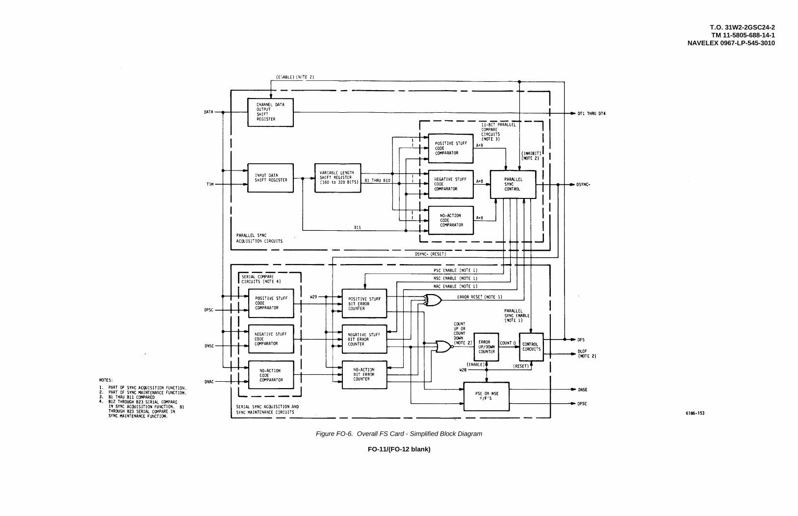
T.O. 31W2-2GSC24-2TM 11-5805-688-14-1
NAVELEX 0967-LP-545-3010
Figure FO-6. Overall FS Card - Simplified Block Diagram
FO-11/(FO-12 blank)

T.O. 31W2-2GSC24-2TM 11-5805-688-14-1
NAVELEX 0967-LP-545-3011
Figure FO-7. FS Card, Primary Shift Register Simplified Block Diagram
Change 1 FO-13/(FO-14 blank)

T.O. 31W2-2GSC24-2TM 11-5805-688-14-1
NAVELEX 0967-LP-545-3011
Figure FO-8. FS Card, VLSR Circuits Block Diagram
Change 1 FO-15/ (FO-16 blank)

T.O. 31W2-2GSC24-2TM 11-5805-688-14-1
NAVELEX 0967-LP-545-3010
6186-108Figure FO-9. FS Card, Serial Sync Acquisition and Sync Maintenance Circuits - Block Diagram
FO-17/ (FO-18 blank)

T.O. 31W2-2GSC24-2TM 11-5805-688-14-1
NAVELEX 0967-LP-545-3010
Figure FO-10. ERD Card, Error Rate Detector Circuits - Block Diagram
FO-19/ (FO-20 blank)

T.O. 31W2-2GSC24-2TM 11-5805-688-14-1
NAVELEX 0967-LP-545-3010
Figure FO-11. Overall Power Supply - Block Diagram
FO-21/ (FO-22 blank)


PIN: 032073-000

This fine document...
Was brought to you by me:
Liberated Manuals -- free army and government manuals
Why do I do it? I am tired of sleazy CD-ROM sellers, who take publicly available information, slap “watermarks” and other junk on it, and sell it. Those masters of search engine manipulation make sure that their sites that sell free information, come up first in search engines. They did not create it... They did not even scan it... Why should they get your money? Why are not letting you give those free manuals to your friends?
I am setting this document FREE. This document was made by the US Government and is NOT protected by Copyright. Feel free to share, republish, sell and so on.
I am not asking you for donations, fees or handouts. If you can, please provide a link to liberatedmanuals.com, so that free manuals come up first in search engines:
<A HREF=http://www.liberatedmanuals.com/>Free Military and Government Manuals</A>
– SincerelyIgor Chudovhttp://igor.chudov.com/
– Chicago Machinery Movers