afwl-tr-80-3285 - defense technical information center · afwl-tr-80-3285 in u controlled ... secut...
TRANSCRIPT

AFWL-TR-80-3285
IN
U CONTROLLED AVALANCHE TRANSIT-TIM TRIODE AMPLIFIERS
S-W. Lee
Electron Physics LaboratoryDepartment of Electrical and Conputer EngineeringThe University of MichiganAnm Arbor, Michigan 48109
November 1980
TECHNICAL REPORT AFVAL-TR-80-1185
Interim Report for Period July 1977-July 1980 D T IC_ ELECTE
APR 0 8
Approved for public release; distribution unliuited.
S AVIONICS LABORATORYAIR FORCE WRIGHT AEONA TICAL LABORATORIESAIR FORCE STSTU CNODWRIGHT-PATflRSON AIR FORCE BASE, OHIO 45433
LIM
*14i

NOTICE
When Government drawings, specifications, or other data are usedfor any purpose other than in connection with a definitely relatedGovernment procurement operation, the United States Government therebyincurs no responsibility nor any obligation whatsoever; and the fact thatthe government may have formulated, furnished, or in any way supplied thesaid drawings, specir-cations, or other data, is not to be regarded byimplication or otherwie as in any manner licensing the holder or anyother person or corporetion, or conveying any rights or permission tomanufacture use, or sell any patented invention that may in any way berelated thereto.
This report has been reviewed by the Office of Public Affairs(ASD/PA) and is releasable to the National Technical Information Service(NTIS). At NTIS, it will be available to the general public, includingforeign nations.
This technical report has been reviewed and is approved forpublication.
E. GRIGUS, VAPT, USAF ALAN R. MERTZ, CAPT, USAFPYoject Engineer Chief, Microwave Techniques &Microwave Techniques & Applications Gp
Applications Gp Avionics Laboratory
FOR THE ClANER
DONALD S. HMS, Chief-Microwave Technology BranchAvionics Laboratory
If your address has changed, if you wish to be removed from ourmailing list, or if the addressee is no longer employed by yourorganization please notify AFWAL/AADM, W-PAFB, OH 45433 to help usmaintain a current mailing list.
Copies of this report should not be returned unless return is required bysecurity considerations, contractual obligations, or notice on aspecific document.
AIR FORCEJIS7Sj A"m aM - -1
= -- ~-==+
_ __ __ ____ _ _ __ ___ A

tWPEF RMING OR AIZ ToN MEAND ATIRES PAGE R EG A D EL MNTR CT TAIN _
'S.~~~~EFR OISTRPuUMjIw FORMET(f 5 Aa
Pont DITRSUIO STATEMEOT NOf 3. RECIPENT' CATALOG owBec 0.I *sz u A
ISPSPLEETARY NOTESq:sThe fidnsi hsrpr re o ob osruda noca
aInhorize documents.
ColletoRf* transit-tim Noc.anis5
The niers. sith figa 3de 5er car1wu ire oaciethsobnjecti MI 8s.
ONTOLN oFic NAM EDAND FOE 51 OSOIT
SE211 ~ CLASSIICATI R orNI PAE wS On a-u
Air_ Foc Sysem J.25900W~ H 543 1
NOMRNGAENV-af AONW1 nws1_ M ____1, N11O .SCRT CAS . t W
SECURITY CLASSIFICATION OF THIS PAGER(Nab DOMa Ena.,i)
20. Abstract (Cont.)
A dc computer program was developed which calculates the dc avalanchemultiplication factor vs. base-collector do bias characteristics. The resultsprovide an estimation of the suitability of various semiconductor materials,optimum collector geometrical structures and doping densities.
Analytical models of dc and small-signal characteristics for Read-type collector
structures are given which incorporate both the avalanche multiplication andcollector transit-time mechanisms. Contrary to previous findings, the -mall-signal characteristics indicate that a large avalanche multiplication factordecreases the RF power gain of small-signal Class A CA7T amplifiers. Theresults are given and discussed.
A large-signal computer simulation was developed which consists of three computerprograms: the emitte,-base computer program (EBCP), the large-signal simulationprogram (LSSP), and the coilector circuit computer program (CCCP). The effectsof high impurity doping level in the emitter, high injection level in the base,time-varying width of the neutral base re.on, carrier-induced drift field inthe base, nonzero minority carrier concentration at the edge of the base-collector depletion region in the base, and the feedback hole current areincorporated in EBCP. Computer program LSSP models the semiconductor regionthrough a set of difference equations of the semiconductor equations. Acurrent-conserving boundary condition is given. The simulation includes thevelocity-electric field, diffusion-electric field, and avalanche ionizaticnrate-electric field characteristics in the collector region. The computerprogram CCCP incorporates the displacement current in the collector semiconductorregion and the effects of the external load impedance.
Large-signal results of Class C CATT amplifiers are obta-ined and are presented.Effects of base-collector dc bias, load, collector structure, and operatingfrequency are discussed. The stimlation calculates amplifier output power,gain, and efficiency. It also gives the emitter-base current and voltagewaveforns; avalanche multiplication factor; waveforms of voltag across thebase-collector depletion region and collector terminal current; and spatialdistributions of electrons, holes, and electric field at any time instant.Large-signal output power, gain, efficiency, dynamic range, and inherentbandwidth of Class C CATT and BJT amplifiers are compared and suggestions forfurther studies are given.
SECUt TY CL&SS1IFCA1II Of THIS PAG.IMSM DMS 4m
I

Th 0S report describes the investigation of simulation studies
at the Electron Physics Laboratory, Department of Electrical and
Comnuter Engi,eering, Te University of Michigan, Ann Arbor, Michigan.
Te work was sponsored by the Air Force Systems Command, Air Force
Avionis JX£Doiator., Wright-Patterson Air Force Base, Ohio underNo. 5i-C-1132
e wok reported herein was performed during the period July
197 to July ±9" by mr. Shiuhi-Wuu Lee. The report was released by
the author n Seitember o ,
The author wishes t hank Professor 3. I. Haddad for his
Suggestion of "'edissertation topic and for his guidance and helpful
suggestions during the course of the investigation and Professor lio A.
Masnari for his helpfual guidance and encouragement. He is also grateful
to Dr. M. Z.1-lta and Dr. .. K. Maina for their assistance in the
comuter simulation oro-nri.
SAcces5si~ o?
1 iulTAB
I ribU'iOU/_ddd
A ailY aaIr
fjt Specia
'itr
jk

TABLE OF CONTENTS
CHAPTER I. INTRODUCTION i
1.1 Historical Background 1
1.1.1 Bipolar Junction Transistors (BJTs) 11.1.2 Controlled-Avalanche r'rhansit-Time
Triode (CATT) Devices
1.2 Basic Properties of CATT Devices 6
1.2.1 Collector Structures of CATT Devices 61.2.2 Principles of Operation of CAT Devices 61.2.3 Comparison of Collector Efficiencies 2nBJT, CATT and IMPATT Devices 12
1.3 State of the Art of BJT and CATT Amplifiers 1?1.4 Outline of the Present Study 25
CHAPTER II. MATERIAL PARAU'TRS AND THE DCr AVALANCHEMTIPLICATION FACTOR 27
2.1 Introduction 2T2.2 Material Parameters 272.3 Dc Multiplication of Charge Carriers in n-Type
and p-Type Si and n-TYpe GaAs CATT Devices 322.3.1 Derivation of the Analytical Expression
for the Dc Avalanche MultiplicationFactor of CATT Devices 322.3.2 Dc Avalanche Multiplication Factor vs.V Characteristics in n-TIype and p-lype"TSi and n-Type GaAs CATT Devices 372.3.3 Effects of Collector Structure of MA
vs. V T Characteristic of n-T'jpe Si 0
CATT Devires 46
V
-% __

-- a e
2.3.3a Effects of Different DopingDensities N h8av
2.3.3b Effects of Different DopingDensities Nd if48
2.3.3c Effects of Different DriftRegion Widths 55
2.3.4 Temperature and Space-Charge Effects in
n-Type Si CA IT Devices 55
2.4 Suimary 60
CHAYTER Ii. DEVICE PHfSICS, DC AND SMALL-SIGNALANALYTICAL MODELS 64
3.1 Introduction 643.2 Dc Analytical Model 65
3.2.1 Carrier Concentration in BJT and CATTDevices 65
3.2.2 Base Spreading Resistance 723.2.3 Dc Computer Model 72
3.3 Small-Signal Analytical Model 763.4 Dc and Small-Signal Results 933.5 Operation of a CATT as an I!PATT with Variable
Equivalent Thermally Generated Current 1093.6 Conclusions 110
CHAPTER IV. LARGE-SIGNAL COMPUTER MODEL lii
4.x Introduction in.2 Development of Device Simulation 1
4.2.1 General Description il4.2.2 Emitter-Base Circuit Model and Computer
Program EBCP 1134.2.3 Collector Region Large-Signal Model and
the Collector Simulation Subroutine CCP 126
4.2.3a Equations to be Solved and theSimulation Technique 126
4.2.3b Subprogram LSS 130h.2.3c The Difference Equations in
Computer Subprogram LSSP 1324.2.3d Subprogram CCCP 139
4.2.4 Iteration Scheme Which Couples theEmitter-Base Region and the CollectorRegion Simulations 140
Vi

Page
4.3 Sample Results l4(04.4 Improvements Over Previous Large-Signal
Simulation of Class C CAT Amplifiers 143
4.5 Conclusions i44
C'7A-FR V. LARGE-SIGNAL SfiDIES FOR CLASS C CATTAF LIFIERS ANitD COMPARISON WITH CLASS C
BJT AMPL FI-IZI 145
r. Introduction 1455.2 Large-Signal Simulation Results for Class C
CA?2 Am!lifiers 145
5.. General D'iscus-on 145
5.2.2 O-ptimum Load lh65.2.3 Dc Bias 1905.2.4 Effects of N , w, and wD
av av driftin HI-ID Collector Structures 156
5.2.5 Uniformly Doped Collector Structures 166
5-3 Large-Signal Simulation Results for Class CBjT Amlifiers 176
5.4 Comparison Between the Class C CAT Amplifierand the Class C BJT Amplifier 180
5.. RP Power Gain and Efficiency atf = 12.75 0Hz and Vsig(t) =
l.l sin t- 0.191 V 1805.4.2 Dynamic Range 1815.4.3 Inherent Bandwidth 183
5. Conclusions 187
CHAT-- eW. SIMIpy, M1051 WD ..SESIONS FORl S Y 188
6.1 Siinary and Conclusions 1886.2 Suggestions for FurLther Study 189
R M CM 191
Vii

i. D mping and Electric Field Profies of Various-CAT Collector Structures. 7
i.'2S -e c Structural Dia of a CAT Device. 8
1.3 Voltage and Currn t Wavefori in the CATT Device.ai B5ae-Coilector Terinal Voltage and (b)induced External arrent. lh
Xi± Collector HF Voltage and Tnduced CurrentWaveforms of F , CAT and M(P1AT Devices. 16
1.5 Norlized P Curves of CAC and TIAPAITout
jjy--ce at Different win&'
1.6 Norm-l' ed Collector Efficiency Curves of CAT?and Il4-A7- Devices at Different 19
D A- Inhe ltipiatio Fact Correspond-- to tario Ionization Fates for Electrons
and Holes at 27 0 C for Two n-?Tee Si CollectorStructures, Ulere Electrons Initiate theAvalanche Process. (Uniformly Doed CollectorStructures 1
D Aanhnrte *aMtinPl atri Factors Corresnond-Zrg 4 I.ar -ous ionization Bates for Electrons andHoles at -1-9 for -to o-Tv_.e Si CollectorStrt rture., Were Holes nit'ate the Avalancheri_-ree. (M fo u--Ly D-pe Collector Structures) 31
De A ach Mtlvicati--n Factors Correspond-ing to Various ionizatic Rates for Electronsand Holes at 200C f '- n.-r- GaAs CollectorStructures, Where Electm- Initiate the AvalancheProcess. (Uniform ly D-ed =ollector Structures) 33
- tematic of te cle rr and fole Particle
Current Distributions :n a Normally Biased n-?-peC-T-Dev ce. (Electron artile Currents HaveOppoite Senses of Detection to that of ElectronicCurrents)
viii
-N=
Figuree
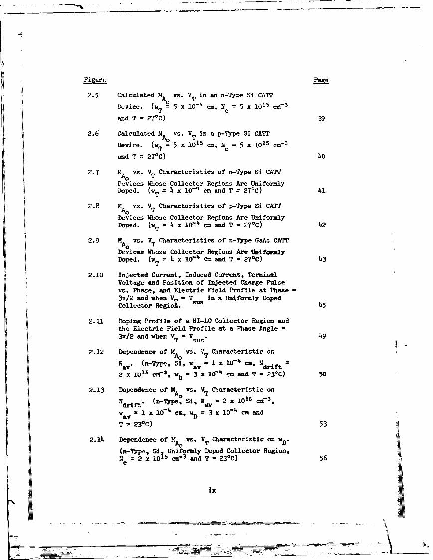
2.5 Calculated M vs. V in an n-Ty-pe Si CATTA0 T
Device. (wT __ 5 x l0 74 cm, Nc 5 x 10 1 5 c - 3
and? = 270C)
2.6 Calculated M vs. V in a p-Tjpe Si CAT?
Device. (NT = 5 x 10 S cm, Nc 5 x 10 1 5 ct - 3
and T = 270C) 1O
2.7 . vs. Vr Characteristics of n-iYpe Si CAT?Ra IDevices Whose Collector Regions Are Lniformly
Doped. (wT= xl - cnandT2rc) h4
2.8 M vs. VT Characteristics of p-Type Si CAT?A0 TDevices Whose Collector Regions Are UniformlyDoped. (wT x10- cm andT2rC) .2
2.9 Mo vs. V Characteristics of n-Type GaAs CATTA0 T
Devices Whose Collector Regions Are UnlformlyDoped. (wT = 4 x 10⁻⁴ cm and T = 2t'C) 43
2.l0 Injected Current, Induced Current, TerminalVoltage and Position of Injected Charge Pulsevs. Phase, and Electric Field Profile at Phase =
3:-/2 and when VT = V in a Uniformly DopedCollector Region. 1 1.5
2.11 Doping Profile of a HI-LO Collector Region andthe Electric Field Profile at a Phase Angle f3-/2 and when VT = V . 49
2.12 Dependence of Mo vs. V Characteristic onAO T
Nv (n-Type, Si, - 1l0-4 cm,% 1 .f =
2 x 10 1 5 cm 3 wD 3 x I andT 230C) 50
2.13 Dependence of MA vs. VT Characteristic onN4im" n-Type, Si, N a 2 x i016 c - 3,
w I x 0 cm, wD =3 x 10⁷- cm and
T = 23t C) 53
2.1 Dependence of M vs. VT Characteristic on VD.*A0
(n-Type, Si Uniformay Doped Collector Region,f 2 x 10¹⁵ cr 3 and T 23C) 56C
ix 7

'IePage
.1 e.ndence of M. vs. VT Characteristic on
Temperature. (n-Type, Si, Uniformly DopedCollector and w- = 5 x 10- ) 59
Effect-- of Space Charge. (n-T-pe, Si, wavlxl cI- 1,dri ft 2 1 c 3 , x0D =3 x 10- 4 cT = 23 0C) 01
.lT Dependence of the Electric Field Profile onSpace-Charg~e Density, N andliav ]drift"
(0 < j < <J ) 621 2 3
3.1 Cne-Dimensional nun Transistor Structure. 66
3.2 Cross Section of Single-Emitter Stripe in anInterdigitated Transistor Structure. 73
3. _ Calculation of Comon-Base CollectorCharacteristics. (a) Dc Device Model and(b) Block Diagram of Dc Program DCCP. 7
3.4 (a) General Device Collector Structure and(b) Electric Field and Current Conventions. 80
3.5 Electric Field Profile Under RF Conditions. 84
3.6 Smal-Signal .Models. (a) Device Model and,b) Circuit Model. 85
3.7 Linear Active CA?! Circuit. (P = the Power
A-ailable fram the Source and P = the PowerAvailable to the Load) avo 90
. ornnh-Base Characteristics. (n-Type, Si,= i x 10 ra4cm, a = 2.5 x 10 16 cM-3,
wD- = 3 x - ,ri 2 x 10 1 5 c= 3
and? = 30 K) 94
3-9 C on-Base Characterlstics. (n-.h'e Si,wv = 1 x 16-4 c=, Ha = 1.5 x IL"- .--Mav 0 c,
w =3 x 1074 CM .dif = 2 Xi ,-- dri-ft
and T = 3000 K) 95
£
gI
- -

Figuree
3.10 Coan-Base Characteristics. (n- ype Si,
w = ]x I0- 4 CM c ,N 2 x 10 16 em-3aV aV
WD = 3 x 10- 4 en, N 2 x 10¹⁵ c - 3
and T = 300°K) 96
3.11 Maximum RF Power Gain and U vs. Frequency.(vT = 4 x 10- cm and VEn = 0.7 V) 98
03.12 Maximum Operating Power Gain and U vs.
Frequency. N T = 4 x 10-" em and VEB = 0-8 V) 990
3.13 Maximur RF Power Gain and U vs. Frequency.(w = x 10-4 - and V., = 0.85 V) 100
03.14 Maximum Operating Power Gain and U vs.
Frequency. (VT = s x 1- cm and VEB = 0.9 V) 1010
3.15 Maximm Operating Power Gain vs. Frequency.(V,= xl 0
- cmandMA =5) 1030
3.16 Maxima Operating Power Gain and U vs.Frequency when Avalanche Multiplicationof Carriers Corresponding to J Is
nEoIgnored. (vT = 4 x 10- cm and = O.7 V) 105
03.17 Maximm Operating Power Gain and U vs. Frequency
vnen Avalanche Multiplication of CarriersCorresponding to J Is Ignored. (NT =nde
x 16-" cmand Vit = 0.85 V) 106LB3.18 Maximm Operating Power Gain and U vs. Frequency
when Avalanche Multiplication of CarriersCorresponding to JnB is Ignored. (v, =
Sx 10- 4 cm and MA = 5) 1070
3.19 Schematic Plots of Jn, V, First Cosponent of
J. " and Second Component of JT ".1081 1
4.1 Circuit Model for a CAT!' ftplifier in theConmon-Base Configuration. 112
4.2 (a) Space-Charge Distribution in a p-n StepJunction and (b) Voltage Distribution in a p-nJunction; A Voltage - V Is Applied to then-Region. VBI Is the Junction Built-In Potential. 116
Xii
N I
-- ~-ff

Figure
4.3 Equivalent Circuit for the Emitter-BaseRegion. 125
h.h The Collector Iteration Scheme. (a) i IsT
Calculated by Using LSSP with V Known andT
(b) Icc and VT Are Calculated, with VCB, IT
Cc and ZL known, by Using CCCP. 127
4.5 Block Diagram of Large-Signal Subroutine CCP. 129
4.6 Equations Solved and Sequence of Steps. 131
4.7 Space-Time Mesh Used to Write the DifferenceEquations. (a) Space Mesh. (b) Space-TimeMesh. 134
4.8 (a) Collector Region, (b) JE(x)I Profile and(c) Electron ar.d Hole Concentration Profile. 138
4.9 Block Diagram of the Complete Large-SignalSir.ulation Program. 141
4.10 (a) JnB' JT and VT Waveforms and (b)
Distribution Plots of Electron Density(Minus Signs), Hole Density (Plus Signs), andElectric Field Profile (Solid Lines). (xxxRepresents the Region Where the Electric FieldHas Reversed Its Direction) 142
5.1 (a) JT and VT Waveforms when RL Is Optimum
(Gp = 9.74 dB, n = 55 Percent, VRF = 31.3 V
and MA = 1.036). (b) JT and VT Waveforms when
RL Is Greater than the Optimum Value (Gp =
915 dB, n = 52 Percent, VRF = 33 V, MA = 1.053).(DEV:Si,n,B,6 x 1015,2; f = 12.75 GHz; V . (t) =1.1 sin wt - 0.191 V; Vbias = 40 V) s1g 148
5.2 (a) JT and VT Waveforms when RL Is Optimum
(G = 10.75 dB, n = 43 Percent, VRF = 27.2 V
and MA = 1.107). (b) JT and VT Waveforms when
RL Is Greater than the Optimum Value (G = 7.37 dB,
n = 20.9 Percent, VRF = 28 V and MA = 1.67).
(DEV:Si,n,B,6 x 1015,2; f = 12.75 GHz; V sig(t) =1.1 sin wt -0.191 V; Vbias = 45 V) 151
xii
NEW

5.3 JT and VT of a Typical 4 x 10- 4 cm Collector
Device Operating at 12.75 U1hz and MaximumAllowed RF Voltage Amplitude. (a) Dc BiasBelow the Optimum Value, (b) Dc Bias Above theOptimum Value, and (c) at Optimum Dc Bias.(DEV;Si,n,B,6 x 1015,4) 155
5.4 (a) Electric Field Profile and Electron andHole Distributions at Various Phase Angles.(b) JT and VT Waveforms. (DEV:Si,n,B,6 x 1015,4;f =12.75 GHz; Vbia= 65 V; VSig 1.05 sin wt -
0.1823 V; and xxx Represents the Collectrr RegionWhere the Electric Field Is Negative) 158
5.5 (a) Electric Field Profile and Electron andHole Distributions at Various Phase Angles.(b) JT and VT Waveforms. (DEV:Si,n,B,6 x 1015,4;
f = 12.75 GHz; Vbias = 6 5 V; Vsig = 1.2 sin wt -0.2083 V; and xxx Represents the Collector RegionWhere the Electric Field Is Negative) 159
5.6 (a) J and V Waveforms and (b) Electric FieldT TProfile and Electron and Hole Distributions atVarious Phase Angles. (DEV:Si,n,B,2.2 x 1016,1.1,7.5 x 101',2.9; f = 12.75 GHz; V
Sig1.1 sin wt - 0.191 V; and xxx Represents theRegion Where the Electric Field Is Negative) 169
5.7 (a) JT and VT Waveforms and (b) Electric FieldProfile and Electron and Hole Distributions atVarious Phase Angles. (DEV:Si,n,B,2.2 x 1016,1.1,7.5 x 1014,2.9; f = 12.75 GHz; V . =
s ig1.2 sin wt - 0.208377 V; and xxx Represents theRegion Where the Electric Field Is Negative) 170
5.8 (a) JT and VT Waveforms and (b) Electric Field
Profile and Electron and Hole Distributions atVarious Phase Angles. (DEV:Si,n,B,2.2 x 1016,1.1,4 x 1015,2.9; f = 12.75 GHz; Vsjg
1.1 sin wt - 0.191 V; and xxx Represents theRegion Where the Electric Field Is Negative) 171
xiii

f j~z~rePage
5.9 (a) JT and VT Waveforms and (b) Electric Field
Profi1le and Electron and Hole Distributions atVarious Phase Angles. (DEV:Si,n,B,2.2 x 1016,1.1,4 x 1015,2.9; f = 12.75 Gliz; V Sigsig
1.2 sin wt - 0.208377 V; and xxx Represents theRegion Where the Electric Field Is Negative) 172
5.10 Power Gain and Efficiency vs. Input PowerCharacteristics of Various CATT and BJTAmplifiers. 182
5.11 Class C CATT Amplifier Performance vs.Frequency at Constant Input Power Level.(DEV:Si,n,B,6 x 1015,4 and Vbias = 63.5 V) 184
5.12 Class C BJT Amplifier Performance vs.Frequency at Constant Input Power Level.(DEV:Si,n,B,2 x 1015,4 and Vbis = 70 V) 185
5.13 Class C BJT Amplifier Performance vs.Frequency at Constant Input Power Level.(DEV:Si,n,B,6 x 1015,2 and Vbi = 37.5 V) 186
xlv
_ _ __ _ l-

4
LIST OF TABLES
Table Page
1.1 Electrical Characteristics of Microwave PowerBipolar Transistors (Commercially Available)for Class C Amplifier and Oscillator Operations(Teszner and Teszner4 2). 21
1.2 Electrical Performances of Microwave PowerBipolar Transistors, with or Without InternalMatching, for Class C Amplifier Operation(Teszner and Teszner 2). 22
1.3 Electrical Characteristics of Microwave PowerBipolar Transistors (Commercially Available)for Class A Amplifier and Oscillator Operations(Teszner and Teszner42 ). 23
l-4 Electrical Performances of Microwave PowerBipolar Transistors, Without Internal Matching,for Class A Amplifier Operation (Teszner andTeszner42 ). 24
2.1 Material Parameters for Si. 28
2.2 Material Parameters for GaAs. 29
2.3 V and M at Different Dc Biases (ExtractedRF A0
from Fig. 2.12). 51
2.4 Data VRF and M Ao at Different Dc Biases
(Extracted from Fig. 2.13). 54
2.5 VRF and MA at Different Dc Biases (Extracted
from Fig. 2.14). 57
3.1 Emitter-Base Structural Parameters. 147
5.2 Effects of De Bias on Amplifier Performance. 153
5.3 Variation of Optimum Dc Bias with Emitter-BaseSignal Level. 157
5.4 Variation of Optimum Dc Bias with OperatingFrequency. 160
xv

Table:Pg
5.5 Effects of R~ on the Performance of Class C
CA~iri Anmli iers. 161
F5.6 Effects of Drift Region Width. 164
5.7 Effects of Ndrift' 167
5.8 L,-i-ge-Signal Simulation Results of CATiTdevices with Uniformly Doped CollectorStructures. 173
5.9 Large-Signal Simulation Results of Class CB.JT Amplifiers. 177
xvi

LIST OF SYMBOLS
A Ionization constant (cmz&').
A Effective device cross-section area in one-dimensional simulation (czn2).
A~ A Ionization rates for electrons and holes,n p respectively (cm'1).
B.3 Input and output susceptances as defined inin outFig. 3.6.
3..,B. Load and source susceptances as de"Ine-d inFig. 3.7.
3. Optimum load and source susceptances for~opt opt maximum operatiLng gain.
3w1 lW1 Device inherent bandwidths at the input andin out output ports as defined by Eqs. 3.76 and 3.77.
b Ionization constant (V/cm).
izi Small-signal susceptances as defined by Eq1s..L1 3.54 and 3.55.
b nb pIonization constants for electrons and holes,n ~respectively (cm 1 ).
C C. Capacitors associated vith the bazze region asb' i~ defined by Eq. 4.26 (F).
C0 Base-collector depletion capacitor (F).
C DE Emitter-base diffusion capacitor ()
C DEFFEffective emitter-base diffusion capacitorCDE~ defined by Eq. 4.21 (F).
C_ Load capacitor (F).
C Emitter-base depletion capacitor (F).
D ,D Diffusion coefficients of electrons and holes,n p respectively (cn 2 .s-1).
D ~Drift field effect including effective electronnEFF diffusion coefficient fcm2 5s 1 ).
d Lateral separation between adjacent emitter andbase fingers (cm).
xvii

de When used as a subscript of a current or
current density indicates a de quantity.
Electric field intensity (V/cm).
Breakdown electric field intensity (V/cm).
E Electric field intensity in the hifh-field regionof a head-type collector structure (V/cm).
S~Minimum Aectric field intensity required tosustain charge carriers at their saturation
drift velocity (V/cm).
-sus rssus Minim u electric field intensities required ton p sustain electrons and holes at their
saturation drift velocities, respectively(V/CM).
SElectronic charge (1.6021 x io19C).
f Frequency (Hz).
max Maximum frequency of oscillation above whichnfl operating power gain is less than or equal to 1
(Hz).
4- Avalanche generation rate (cm-3-s - 1 ).
L "in cout- Input and output conductances as defined inin outFig. 3.6.
Load and source conductances as defined inFig. 3.7.
-i , Optim-m load and source conductances for maximuaopt opt operating gain.
Operating power gain (dB).
Smll-signal conductances as defined by Eqs. 3.5hand 3.55.
h,w Widths of base fingers and emitter fingers,respectively (cm).
When used as a subscript indicates a differenceequation field point.
13 Base current (A).
ICiCTE--- Coliector current, collector displacement current,emitter-base diffusion current, emitter-base
displacement current, respectively (A).
xviii
I - --

I SIcP Electron collector reverse saturation currentns ps and hole collector reverse saturation current,
respectively (A).
IEIET Emitter particle current and emitter current,respectively (A).
InB'InE Electron current injected into the collectorregion and electron emitter current,respectively (A).
DB_ II-Ep Hole feedback current from the collector regionand hole emitter current, respectively (A).
I, Induced collector particle current (A).
When used as a subscript indicates a differenceequation space-charge point.
Jsubscript Current density (A/cm2 ).
K When used as a superscript indicates a differenceequation time point.
k Boltzmann's constant (1.380 x 10 - 23 J/iK).
T Load inductor.
L ,L Diffusion lengths of electrons and holes,respectively (cm).
t Length of emitter fingers (cm).
MAMA Average multiplication factor under dynamico operating conditions and dc multiplication
factor, respectively.
N N Acceptor and donor impurity doping densities,A 1respectively (cm- 3).
N 'N -Doping densities in the high and low regions ofav drift a HI-LO collector structure, respectively (c 3 ).
Nc Doping density in a uniformly doped collector
structure (cm 3 ).
n Electron density ( 0 -3).
n Thermal equilibrium electron minority carrierconcentration (or).
xix!_ -X
'1

5.. Electron density at the base-collector
m-tallurgical Jtuiction (cmr 3 ).
De electron Censitv (cmf3).
3emiconductor intrinSic carrier dens-it (cm i.
;ers avialears the output termaial andtheinpt ermna, rspectlvl.asdefined
in Fig. 3.7 (W).
dcDc power dissipation in the collector region W
~n utInput and output power (W).
Hole density- (cZ-3).
_0Thermal equilibrium hole minorit_ carerconcentration (di- 3 ).
Hole density at the base-collector metall"urgicalJunction (cm 3 ).
Dc hole density (cm 3 )Ydc
Quality factor of the tank circuit load.
Charges stored in the neutral base region, oneach side of the emitter-base depletion region,and in the doping clump of a LO-HI-LO collectorstructure, respectively.
Equivalent base region spreading resistor.
R Resistors representing the resistances associatedb bb with the base region between adjacent emitter
and base fingers and the base region directlybeneath the emitter fingers,* respectively.
R. Load resistor.L
S Linvill stability factor as defined by Eq. 3.68.
T Temprature.
T Time period of a cyclical quantity (s).
U A measure of the degree of activity of anplifiersas defined in Eq. 3.66.
V ,V Voltages corresponding to the minium and1 2 maximm points of the RE voltage across the
collector depletion region, respectively MV.
XX

V ,V Small-signal voltages as defined in Fig. 3.6.1 2
V V Small-signal voltages as defin -a in Fi;. 3.6.
VB VB! Vp.1Vsu s Junction breakdown vroltar=e, unction built-inpotential, collector punch-throueh voltage,
and minimum voltage across the c;Al'Uectordepletion region needed to mainc.-An carriers attheir saturation drift veloci-y at -all times,respectively (V).
V bV Base-collector de bias, emitter-base inputs sigA sigzml, and small-signal nl- tter-base input
signal, respectively (V).
V',V. 3 V . Voltages across the emitter-base terminal,emitter-base depletion region, base-collector
Junction and the load, the load, and t he base-collector depletion region, resveciveiy (V).
'Vn p Drift velocities of electrons and holes,respectively (cms-1 ).
v ,v Saturation drift velocities of electrons andholes, respetively (cc-t--)
v Carrier saturation drift velocity (cm-s-l).s
w ,v ,w Boundaries of depletion regions as defined in1 2 3 Fig. 3.1.
IaW Widths of the high and low doping regions of aHI-LO collector structure, respectively (cm).
'vBWB Width of neutral base region and separationo between emitter-base and base-collector
metallurgical Junctions, respectively (cm).
w Width of high doping region of a L06-HI-Wke collector structure (cm).
WEWE Width of neutral emitter region and depth ofo the emitter-base metallurgical Junction,
respectively (cm).
VT Width of the whole collector region (cm).
Collector depletion width when VT = V
X'y Space coordinates in the collector region andthe base region, respectively (cm).
xxi
N-'

Y-3- ,Width of base region beneath the emitter finger
1 2 and the depth of emitter-base metallurgicaljunction from the device surface, respectively(cn).
" in' out Input and output admittances, respectively.
V -v Load and source admittances, respectively.
Device small-signal y-parameters defined by13j Eqs. 3.48 and 3.49.
y Device small-signal y-parsmeters defined byEqs. 3.54 and 3.55.
ZL. Load iuedance.
0 When used as a subscript of a voltage or anelectric field quantity indicates a de quantity.
When used as a subscript for a current, avoltage or an electric field quantity representsa small-signal RF quantity.
Ionization rates (c-).
2 De ionization rates (cr -).0
a Dc con-base current gain.0
a. Dc emitter injectin efficiency and dc basetransport factor, respectively.
B Dc cozn-eitter current gain.
Amplifier input tunability.
Dielectric permittivity (F-cC 1 ).
Amplifier efficiency (percent).
If cCollector de to ac conversion efficiency (percent).
aWe "Tr ansit angles of the drift region and the wholecollector, respectively.
ai._. Sc Phase angles associated wit. carge injection anddelay of charge injection due to space charge,
respectively.
Electron and hole nobility, respectively.
xxii
HI!
L __

p Resistivity (. -cm).
Conductivity in the base region (mho-c -1 ).
T-e Delay time in responses due to heavy impurityC doping level in the emitter region.
T Tranit time in the carrier generation region.6
T Lifetimes of electron minority carriers and holeminority carriers in p- and n-type semiconductors,r'spectively (s).
Dielectric relaxation time.
* PoteniMl variation in p-n Junction depletionregion.
" i xxtii
MOW A'

C3IA1SrE 1. lNTRODUCM01Y
1.1 Historical Backgrouna
1.1.1 3inolar junction T-ansistors {BJ7s). Of all
semiconductor devces the BYT, an acronym for bipolar junction transistor,
is the most important. Its invention brought about an unprecedented
grov;th of research and deveio.ent in solid-state phisics and engineer-
1g. Tra.sltors are now key elements, for example, in high-sneed
comuters, in space ehicles and satellites, and in all modern
commnication and porer systems.
development t n nt-contact transistors by Bardeen and
Brattain1 was announced in 198. Then in 1949, Shockley 2 proposed a
junction bipolar transistor and laid out the basic theory of this
fundamental structure, in the microwave power bipolar transistor area,
Pioneering work was done by Ear and Pritchard," where they considered
high-freque - y effects, and Ebers and Ml',5 Fletcher, 6 and Eeis et a., 7
who studied high-power effects on transistor operation. Some papers
have been devoted to the analysis of the mutual dependence of these
effects. 8-10 On the other hand, some more recent studies have been
published concerning the ther and characterization of microwave
bipolar transistors. 1115
At the inception of the .--T, transistors were able to operate
at frequencies up to a few hundred klz o& y and the chioce of the semi-
conductor material was restrict-ed to geranium, since the aterial had
been produced with sufficient purity and in single-crystal form. Theory
= _ _ - _ - - - ~ -- -- 4

predicted that they should be able to operate at much higher frequencies,
even into the microwave frequency range, by a reduction of their overall
dimensions. In particular, it was recognized tt the transit time of
charge carriers through the device and the rate of chae of electrical
charge stored within the device would li the frequency response. In
order to improve the performance at higher frequencies, the base width
of the BJT must be reduced to reduce the transit time and the active
device area must decrease in order to uce the capacitance or stored
charge. These refinements dtmaxred -ucb tizhter control on all three
dimensions of the device. Tasistr tec:ology has enjoyed many break-hrnoughs. particularly in'. the a,- tni 1 6 and grown-Junction tech-
nirus7 part "-ual I ,e
niuues1 7 and in one-refining ,' AffsAn, 19 - 2 1 epitaxi- 2 2 planar, 2 3
bea-lead, 2 ' and ion implantation technol-ies. 25 These breakthroughs
have helped to increase the power and frequency capabilities of transis-
tors, as well as their reliability, by many orders of magnitude.
With the present technology and without electron-bea or x-ray
exposure (i.e., - I ,-n linewidth:, an asrFect ratio of - 20:1 is
theoretically attainable with interd-itated, overlay or mesh structures.I
The practical limit, however, e-*ns to be approximately 10:1. .As to
the base layer width, the low et value ahieveA under a co-promise
between mini= base transit ti and aMmniu= base spreading resistance
is - 0.1 s.
The physical properties of the semiconductor theoretically
determine the "'M e' etr"c paler_-_.zr=c Of he transistor. For
example, Johnson sh-owed- tht -h*max -=a- frecuency of operation will
be proportional to -v ,where n e -Juntim breakdoun electric
field and v is the scatterin-- iii-e -arer dift velo-city. As the

size of the device is reduced to achieve high-frequency performance,
the voltage must be maintained at a value sufficient to give the required
power output. In the limit, a further reduction in device dimension
parallel to the electric field direction would be impossible because the
electric field would exceed EB. In practice, the frequency limit derived
by Johnson has not been reached. For technological reasons, Si is pre-
ferred to Ge and GaAs for microwave bipolar transistors. The techno-
logical superiority of Si is due mainly to the ability of silicon dioxide
to act as a diffusion mask and the ability to etch very fine patterns
in this oxide. The oxides of Ge and GaAs are not as stable as silicon
dioxide and for these semiconductor materials chemical vapor deposited
silicon dioxide and silicon nitride, when used as a diffusion mask or
as an insulating material, produced results inferior to thermally grown
silicon dioxide on silicon. Much progress in GaAs technology has been
achieved in the last few years. Another reason why Si material is
preferred is its good thermal conductivity which is a factor of two
better than GaAs. Good thermal conductivity is a!, important concern,
especially in high-power applications.
Bipolar junction transistors have the following advantages which
assure their place in the microwave power semiconductor device family:
1. Due to their three-terminal configuration, their application,
particularly as amplifiers or switching devices, is much easier and
the corresponding circuits much simpler than for two-terminal devices.
2. Due to their operation with both majority- and minority-carrier
types, very high local current density can be reached, much higher than
in the majority-carrier devices.
-3-

3. The operating power efficiency is high, particularly for Class
C amplifiers.
h. The operational bandwidth is large, particularly for Class A
amplifiers.
5. The power gain in amplifier operation is relatively high.
6. Signal distortion is lower than in two-terminal devices. Noise
level is lower than in avalanche diodes.
7. With present Si technology, good output power can be obtained
in the X-band frequency range.26
1.1.2 Controlled-Avalanche Transit-Time Triode (CAXr') Devices.
Diodes, and in particular the IMPATT, which is an acronym for imact
ionization avalanche transit time, have relatively simple configurations
and operate close to the well-known Johnson8 material parameter limi-
tation. Transistors, however, perform well below the material limit,
in spite of considerable effort to optimize their configurations and
the great advancement made in Si technology. On the other hand, three-
terminal devices have many advantages over diodes as mentioned previously.
A new three-terminal device was proposed by Yu et al.2 7 in 1974. This
new device was named CArT, an acronym for controlled-avalanche transit-
time triode. It is self-evident from its name that this device utilizes
both avalanche multiplication and transit time. In designing a BJT
device, avalanche multiplication has always been associated with junction
breakdown and was always avoided in amplifier applications. Incorpo-
ration of avalanche multiplication into the BJT device is important for
several design applications. 2 8-3 0 For a large number of circuits,
transistor Junction breakdown is used to provide a reference voltage.
~ _ _ _ _ - _ _--

An ability to model such operation is desirable. For other applications,
circuit performance under surge conditions must be determined. Possible
malfunctions due to second Dreakdown, can only be determined if an avalanche
model is first established. Another reason for investigating avalanche
muitiplication is that when a BJT is biased in the avalanche multipli-
cation region, a negative differential resistance between cc-lector and
emitter may exist. This part of the characteristic, cormaonly named the
avalanche region, may be used for fast switching applications.31 in
power amplifier applications, it has been established that BJTs having
long collector regions, i.e., large junction breakdown voltages, can be
desirable, but it was not until the discovery of the CATT device by Yu
et al. 2 7 ,32-3h that both avalanche multiplication and collector transit
time were actively used to advantage in power amplifiers. In 1974,
Winstanley and Carroll3 5 proposed the IMPISTOR, a transistor with an
IMPA"-like collector region, for which Yu et al. have suggested the
name CATT. Carroll36 discussed three possible modes of operation for
the avalanche transit-time transistor: (1) the multiplication mode,
(2) the negative impedance mode, and (3) the pulse mode. The modes
move progressively through the phenomena of avalanche multiplication,
IMATT negative conductance combined with multiplication, and voltage
collapse and high zurrent pulses associated with TRAPATT operation.
The multiplication rode will be studied in this report. Quang, 37 in
1975, presented a lumped-distributed small-signal equivalent circuit
for an IMPISTOR in the negative impedance mode. In 1976, 1efebvre et
al. 38 utilized a computer program developed for high-efficiency IMPATr
diodes 'o investigatc the influence o r a thermionic-type injected
current on the dynamic operating conditions and performance of GaAs
-5-

IMPATT diodes. The work showed that interesting results can be obtained
in X-band and the practical realization of such a device would be possible
by using a CATT operating in the negative impedance mode.
1.2 Basic Properties of CATT Devices
1.2.1 Collector Structures of CATT Devices. The various struc-
tures are described in terms of the avalanche region width Way , the ava-
lanche region doping density Na, the drift region doping density Ndrift,
and the drift region width wD. The LO-HI-LO doping profiles also include
the total concentration of carriers in the charge clump per unit area Qc"
The doping and electric field profiles for various common CATT collector
structures are shown in Fig. 1.1 along with the parameters that are used
to describe their characteristics.
1.2.2 Principles of Operation of CATT Devices. The CAM1 device
operates in a manner similar to that of a bipolar junction transistor.
In an n-type CATT device, whose structure is shown in Fig. 1.2, electrons
and holes are injected across the forward-biased emitter-base junction.
The majority of the injected electrons, minority carriers in the base
region, diffuse across the neutral base region and then the electric
field, set up by the base-collector reverse bias, draws them into the
collector region. A small percentage of the emitter-injected electrons
are lost in the base region through carrier recombination. Electrons
that are drawn into the collector region first undergo avalanche multi-
plication in the high-field portion of the collector region and then
drift across the depleted low-field portion. While making a transit
across the collector depletion region, a current is induced at the
collector terminal. Unlike the bipolar junction transistors whose
,., -6-

p Nc
DOPING PROFILE ELECTRIC FIELD PROFILE
(a) UNIFORM STRUCTURE
~- WT~
way
Ndrlf t
DOPING PROFILE ELECTRIC FIELD PROFILE
(b) HI-LO STRUCTURE
r- WD~
Nay Ndrif t
DOPING PROFILE ELECTRIC FIELD PROFILE
(c) LO-HI-LO0 STRUCTUREFIG. 1.1 DOPING AND ELECTRIC FIELD PROFILES OF VARIOUS CATT
COLLECTOR STRUCT[URES.

C.)
ir L Z 0bo -0
o E--A- E1oCO)o
< ~1
jr CI- H
-8-
__ __ o

&rocn-bae t.J. ent. gain always less than unity, carrier multin-lication
". teC.T- device results in a current gain of the order of two to ten.
Wit% the p-opr doping prol'Ile, a long collector struacture allows the
sustenance c a very large EF voltage across the collector depletion
region. rf.r. CArT anpiifies develon additional newer ga through ava-
ch =ui-hication and b the use of tr"ansit time in the collector.
. ', the nower gain can be much higher than for a birclar
* -or transis-or having an equival ent emitter-base structure, or fonr
same gain at a hznhegr frequency.
Structtural y, tne n-t.pe CWIT device is similar -o an npn bi-
v 01 transistor except for two -ajor differences, as shown in
F. .2. The collector has a high-field avalanche multiplication
--.g on in which the emitter injected electrons are m l'tinlied and a
gdrift region, it should be noted that the long drift region is
usd topovide proper timing for the avalanche multiplication of the
eztter ie e iectronr, besices providing the collector with a
:arge ar votare capability. if the hiad impedance is a high-Q tank
C- nuIn whose resonant frequency equals the emitter-base signal fre-
queny. - e induced current waveform of a common-base Class C CAT
device is such that its fundamental component is automatically w rad
t ofhth w e ne--sinusoidal collector RF voltage regardless
of the co e--tor transit angle 0r. The induced current waveform is£
awavs centered around the phase angle 312 rad of the RF voltage wave-
f On the one *nd, if the collector region is narrow, the induced
utr.n- wave"r will be narrow and the collector efficiency, which is
fined as he .a io of signal power to dc input, is high. On the
-9-
- IN ---

other hand, the emitter injected electrons will enter the avalanche
multiplication region at a time when the voltage across the collector
region is low and not many electron-hole pairs will be generated.
Limited by a narrow induced current waveform and small current multi-
pI -cation, a CATT device with a narrow colIector region will not be
able to produce very much RF ower. if the collector transit angle is
rreater than rad, the emitter in.jected electrons will enter the
aiancn.e .- 'it aplication region at a time when the voltage across
the collector region is nign and carrier multiplicqtion will be large.
A collector transit angle greater than. rad implles that there -s
con-uction current flowing during the positive half-cycle of the
colector K- voltage which means energy dissipation instead of newer
reneration. The collector efficiency is poor for large col±ector
transit angle situations. An optimm operating condition seems to be
when the collector transit angle is approximately r rad.
It should be noted that the collector FY voltage is initiated
by the entering of emitter injected electrons into the collector. This
is because the bias voltage, as seen by the -ollector, drops when the
collector curent flows in the external load, whereas in the DIMPA
ciude, the w rent waveform is initiated by the device voltage whach
is the superpsition of a large K- voltage over a de bis which is ony
si.~tiy below the device Junction breakdown voltage. i" -'e -nave-
charge effect is ignored, theoretically, a pulse of charge is always
1.djected into the low-field drift region at the tine when the phse
angle of tne MPA T RIF voltage is close to u rad, regardless of the
~rif r egion transit angle. The collector voltage and induced current
-10-
I

waveforms of a CATT device and those of an IMPATT are very similar when
the drift region transit angle is approximately a rad and they are dif-
ferent when the drift region transit angle differs significantly from
Srad.
The upper limit on the collector voltage is approximately the
base-collector junction breakdown voltage VB . Actually, the collector
voltage can ex-eed VB slightly for a short duration of time. The lower
limit on the collector voltage is the voltage needed to sustain electrons
at approximately the scattering limited velocity during its entire
mrns1 t across the depleted collector region. For high-power appli-
cations, th optimum base-collector dc bias is such that the collector
car have l large avalanche multiplication factor and a large RF voltage
he dc bias is increased above the optimum value,
tkough m.e current gain would be increased, the amplitude of the
=oiector F voltage will b* decreased due to the upper limit set by
If the d bins is de"ased below the optima value, current gain
ruld A ef 4 be decreased nA possibl, the amplitude of the collec-
F voltago *!:so 4e-ca- Iue tc the lower limit set by the
age requred r Ain = =arri--r nt the scattering limited veloc-
Aopt==-- d bias, the a-a-che multiplication factor of a
typ device ranges from twc to ten rather than a million as
i the IIAI 7 -e. Terefore, when the emitter is not injecting
carriers ito nte collector, the collector current equals approximately
ten time t*h erna.3-y renerated reverse saturation current. A
signifian conduction current exists in the collector only when the
enditter-tse junction is forward biased. This is why it is called a
a U) -:-

The CAfl' is a complicated device for several reasons. The
seemingly simple avalanche multiplication process as emnloyed, for
example, in avalanche photodiodes 3 9 becomes much more conn iex i ". CAL
Aevices due to the large RF voltage swing. The CAT is csrinex fo.
another reason. The avalanche multiplication generated holes win
feed back into the base region and constitute a negative recombination
base current component. This phenomenon results i-n a r ni-rform
emitter current injection and better use of the emitter finger area
than for bipolar junction transistors. If the feedback hole cur ent15 large enough the polarity of the base current is reverse Pinch-
in phenomena rpther than pinch-out phenomena in the base regio' wo=d
occir if the carrier multiplication IS large.
When the collector transit angle equals -a , the signa
carriers are injected at or near the time when the voitage eq S.where VT is the average value of the base-c.. ctor temeel
T T0 0
voltage, if the space-charge effect is negligib.re; e avalanche
plication nrocess is, therefore, almost independent th RF woitae
amplitude. This is an essentia conditin- for a Ie a i .
should also be pointed out that nonlinearity ..i the CA Is de m-
to the exponenti- l turn on of the e-itter-base Iunct'o. as in the
a1b- a certain extent this nonline-a.itv is allev-atd n the IC d
to the fact tha, the space charge win cause the eefective avai =---
m-itinlication to decrease as the input sniaI IS Is-crazva
nis leads to a wider dynamic rane.
1.2.3 Comparison ot Collector Eff.cie... .n fl, 1A7 acn:
i.rA7iT Devices. For the i duced coIIector -a.- t tn I w
N1
- -- _ _ 5Z5= - ~ -\
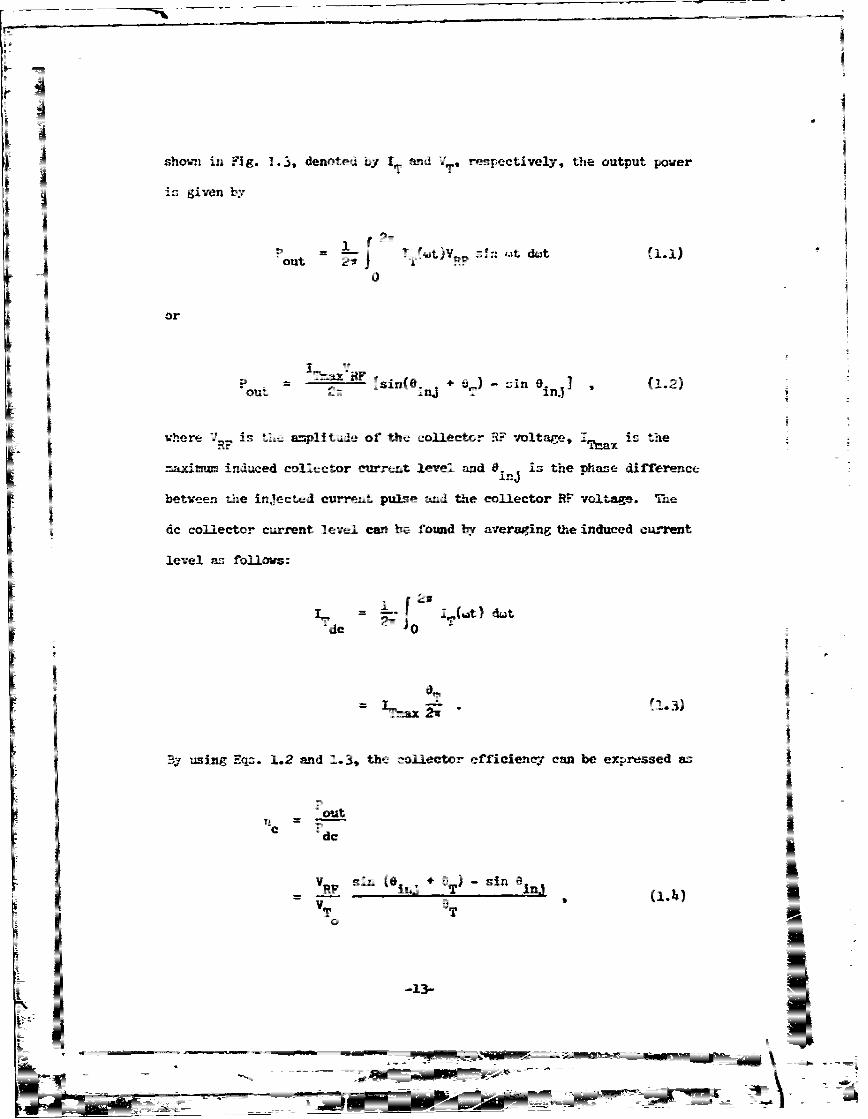
shown in Fig. 1.3, denoted b i and VT, respectively, the output powerT
Is give-. by
_ S~f at Utout -r -
or
nj -5 == . ] 1.2)
where i.s the aniaitude of the collector RF voltage, s themrV-- -Tax
maxiIu induced collector curret Ievel and 8. is the nhase differencein.)
between the injected cu rnt n Pn d tU- collector Mr voltage. Te
de collector current level can br found by averaging the induced current
level as follows:
i --= 1
Tax 2-
B using Eq-s. 2 -and i" tc coli-ector efficiency can be expressed as
+out
=
d--I
si + n 6.
j_ +-1 T-4
U
. .. I+

VT
ITI
oii
Tinax
IS
v/2 ir 3v/2 21r
FIG.1.3vo~a AD CM= WVXFM nIU MT MCII04AC MMILI ~G I b UEI 1NW

where P is the dc input power. The waveforms of V and I for BJT,dc T T'CATT? and L'_PATr devices are shown in Fig. 1.1. A negative Po implies
that PS power is being generated. Both the BJT and CAT? devices are
operating in Class C configuration and t-:- load is a high-Q tank circuit
whose resonant frequency is approximately equal to the signal frequency.
The induced current waveform for the BJT is a short current pulse,
because its collector region is narrow. A narrow collector region also
implies that only a small PF voltage -wing is allowed. From the induced
current waveforms, it is expected that the CAT? efficiency wil be lower
than that of the JT? due to the large transit angle requirement. The
induced current waveforms of the CATT and LWAT corresponding to
various drift region transit angles are shown in Fig. IA Me -a in
indued current level is assmed to be constant. For the CAT, 0 is
alwys given by
in,
and Lip. 1.2 and l.4 become
out2
an-
'I
2
For the LL?!Y 0. s ven by
in is

vI
BJT
o v/2 IF 3v/2 2w
IMATT V
II - - 1o v/2 r 3v/2 2. il
ITI

ii
0.n = - osc (1.8)
where 0 is the injection phase delay due to the space-charge effect.sc
If the space-charge effect is ignored, 0 0 rad and Eqs. 1.2 andSc
1.1i become
I TmaxVRF (I - cos 0T ) (1.9)
out 21 T(
and
V 1- cos 0nc-V T . (1.i0)
TF T0 T
Shown in Figs. 1.5 and 1.6 are plots of P and n as functions ofout c T
at different values of 6 The quantities of Pout and r are normal-inj ou c
ized in terms of I TmaxVRF /v and VRF/VT , respectively. Results indi-0
cate that the CATT P and n are higher thsn the IMPATT due to theout c
fact that the induced current waveform of the CATT is always centered
at 0 = 270 degrees. It is also noticed that the CAnT 3-dB Pout and n
bandwidths are wider than the IMPATT. As 6n decreases due to thei
space-charge effect, the IMPATT normalized P and nc and their 3-dZ
bandwidths also decrease.
1.3 State of the Art of BJT and CATT Amlifiers
Electrical characteristics and performance of microwave power
transistors depend first on the operational mode, i.e., amplifier,
oscillator, and switching, and second on the operational class, gener-
ally Class C or A, in the amplifier and oscillator cases. On the other
-17- _
oI

-Thj
10o
o
I-
0o
0 C.3
-- to
-a- On
0w
9-0 00
0 r.
00
AH XDW.L Ino(A'' A D/

03Cuj
oc
cu
00
w( 0
CiF 0
40
00
0n390N3?3 %z

hand, fre- power performances are influenced through the packaging
conditioi The transistor dynamic characteristics can be seriously
degraded through the package inductances and capacitances. Making
external input and output matching at microwave frequencies is extremely
difficult. The first attempt to eliminate this drawback was to reduce
these inductances and capacitances as much as possible. Two more
sophisticated solutions were developed recently. The first consists
of input and output matching within the transistor packaging, the so-
called chip carriers; the second does away with the package and intro-
duces transistors directly in a microwave integrated circuit called
MC2 0 '4 The first type is commercially available; the second is
currently under commercial development.
The bipolar power transistors have been developed primarily for
Class C applications, because in this class of operation both power and
efficiency attain their highest values. However, in recent years the
field of application of the BJT has been extended to Class A, with a
view to reduce the nonlinearity and noise figures. The output power
of the Class A BJT is also characterized by a large bandwidth and gain
flatness.
Tables 1.1 and 1.2 give the electrical characteristics of BJTs
for Class C amplifier and oscillator operation and the performance of
Class C BJT microwave power amplifiers. 4 2 Similarly, Tables 1.3 and
1.1 give the electrical characteristics of BJTs in Class A amplifier
and oscillator modes and the perform.-nces of Class A BJT microwave
power amplifiers. 4 2 The results in Tables 1.1 through 1.4 represent
the state of the art in 1977. More recently, a Si power BJT for use
-20-

Table 1.1!
Electrical -aracteristics of Microwave Power Bipolar-ransistor (Co Arcially Available) for Class C
Amlifier and Oscillator Operations (Teszner and Tesznerh2 )
Frequency Range (GHz)1-4.5
Collector-base breakdown voltage, BVc (i) 35-TO
Collector-emitter breakdown voltagewith shunted BE junctiona t (V) 35-60
Collector-emitter breakdown voltage (withopened BE juntco.) ,VEP' (V) 15-4o-m-itter-base breakdown voltage, BV CV) 2-
_L - EBOM2-
Collector-emitter continuous voltage, VCE V) 12-28b
Emitter metal finger average current density,'Emfa (A cC 2 ) - 5 x 10-5 x 10 5
a. The shunting must be of sufficiently low resistance to limit theminority carrier injection as much as possible.
b. For CvI operation; in pulsed-wave operation, VEC is generallyincreused, up to 40 V.
" i -21-
- 7 r2,

Table 1.2
Electrical Performances of Microwave Power Bipolar
Transistors, with or Without Internal Matching,
for Class C Amplifier Operationa (Teszner and Teszner 4 2 )
Frequency Range (GHz)
Amplifier transistor 1 2 4 4.2 4.5 6 8 10chip
Output nower in CWoperation(W) outmax 35 20 5 -I 3 d ie 1 5 g 1.2 h h
Amplifier power
added efficiency, f d e2
n (percent) 60 50 30 33 40 25 36 g 2h 2h
Power gain PG (dB) 10 10 5 Tf 4d 4 e 4 .5g 5h 4.4h
a. The data given up to 4 GHz concern commercially available transistors,of both types, with or without internal matching.
b. In pulsed-wave operation, an output power level of 150 W (duty cycle- 1 percent) at 1 GHz with PG = 10 dB is obtained with comerciallyavailable transistors (VcE being increased to 4O V).-
c. The il values indicated here correspond to the Poutmax; however, some
higher values have been obtained for lower Pout; in particular, at
I 0Hz, n goes up to 65 percent and at 2 GHz, up to 60 percent.
d. Internally matched devices.
e. Devices without internal matching.
f. Experimental.
g. Experimental.
h. Experimental.
-22-

Table 1. 3
Electrical Characteristics of Microwave Power Bipolar Transistors
(Commercially Available) for Class A Amplifier and
Oscillator Operations (Teszner and Teszner 42 )
Frequency Range (TIz)1-4
Collector-base breakdown voltage, >BLi (vi=1&
Colector-etitter breakdown voltage,,1 = 15
r itter-base breakdown voltage, BYVK. (V) - 3
Collector-eidtter continuous voltage, -/c (v) =1i5
Col-ector-erntter continuous current, >, ,50
a. For B. the values approzimte B .l .
-3

Table 1. 4
Electrical Performances of Microwave Power Bipolar
Transistors, Without Internal Matching, for
Class A a Amplifier Operationb (Teszner and Teszner 4 2 )
Frequency Range (GHz)
1 2 3 4 6
Amplifier transistor chipoutput power in CW operation,
o (W) 3 1.2 0.8 0.8outmax N
Amplifier tower efficiency,ri (percent)c -30 -25 -20 -15 -17
Power gain PG (dB) c 10 10 8 6
a. A linear amplifier operating in Class B or AB with active broadbandbias circuit has been developed in the laboratory. Compared withClass A amplifiers it would provide for identical I/C (intermodulationratio) = - 20 dB, an efficiency - 2 times higher (15.5 vs. 8.5percent) with PG = 10 dB, Pout = 0.4 W at 4 GHz. This efficiencyratio seems to be increased for lower I/C; thus it becomes - 5 forI/C = - 30 dB, but with q decreasing to 12 and 2.2 percent,respectively, and proportionately PO However, all the efficienciesquoted remain low compared with theefficiencies of commercially
avnilable devices given above.
b. The data given up to 4 GHz apply to comercially available transistors.The data given in the last coluat are for an experimental model,under laboratory development. In both cases the output power isobtained at 1 dB gain compression.
c. The n and PG values correspond to P
-21-
- - - ma

at X-band Za been developed using e-beam and ion implantation. Te
-JT has a bar sze of 0.5 x I m= and consists of' four 2.5 x 75 Um2
active cells. The combined output power of four cells operating in
Class C eonfi jrataon is nearly 2W Ct at 8 G.z and almost 1.5 W CO
ati0G.
nenmen-ta data on Class C CAT amplifiers is very limited.
Tne only pucished results are those by "u et a&.27,33 They demn-
str~a ed t- feasibility of a CATT amplifier both theoretically and
expeeri menally from 0.5 to , GuHz. An S-band CA.T device with an
- tter periphery t- activo base area ratio of 3.3 x 10³ in - I achieved a
a 1 f 1 3 -0 at a pulsed power output of 12 W and 28 percent power
2e2 efficiency when operated at 2 GHz . The gain at this operating
n w. at --- s 11 dB higher than its equivalent BJT transistor. Experi-
menta l results indicate that the impedance levels and Q values of the
CA are faorable for impedance matching, power combining and instan-
taneou bandwidth operation with useful gain.
a utline of the Present S
T h obJective of this study is to investigate the theoretical
capatiity of Class C CAW amplifiers and to compare them ith WT
a-zplifiers. Analytical equation3, circuit models and computer simula-
tions are used to determine de, s=all-signal, and large-signal behavior.
T- .Maner ii a computer program is developed which calculates the
cc avalanche multiplication factor as a function of collector stracture,
base-co iector de bias and -material parameters. Information concerning
optiwma collector structure for large-signal operation and suitability
of various materials can be obtained.
-25-

In Chapter III analytical de and small-signal models for CATT
devices are given. Computer solutions of the analytical models are
given and the results are discussed.
In Chapter IV a large-signal computer simulation is developed.
The simulation calculates the RF output power and efficiency and many
other parameters. Detailed descriptions of the numerical algorit
and the computer programs are given.
M In Chapter V large-signal results are obtained for a series
of X-band CATT and BJ'P devices. The computer results for both devices
are given, discussed and compared.
In Chapter VI a summary of this study is given and suggestions
for f-rther work are described.
-26-
-~ - -

CHAPTER II. MATERIAL PARAMEE AND THE DC
AVALANCHE MJLTIPLICATION FACTOR
2.1 Introduction
As mentioned previously, an ideal CATT device should have a d
bias point at which both a significat avalanche multiplication factor
and a large RF voltage across the base-collector terminal can result.
A simple computer program called AVALAN was developed which provides
information on the do avalanche multiplication factor H as a functionMA
0
of the dc base-collector terminal voltage V , the punch-through voltage0
the breakdown voltage VB' the sustaining voltage V and the"PTB sus
electric field (E) distribution in the collector depletion region. In this
chapter the material parameters, uaw avalanche multiplication factor and
the electric field distribution for devices of different materials and
various structures are given and comparisons are made. The effects of
device temperature and space charge are also described here.
2.2 Material Parameters
The material parameters required to calculate VB V0
and E are a, a," c, S and E s ,s where a and a are the electronSin si i pa p
and hole ionization rates, respectively, c is the dielectric permittiv-
ity, and E and E are the electric fields required to sustainsws suspn p
electrons and holes at their saturation velocities. These values for Si
and GaAs are listed in Tables 2.1 and 2.2. Shown in Fig. 2.1 is the de
avalanche multiplication factors of two n-type Si devices, vhere electrons
initiate the avalanche process. Figure 2.2 shovs the de avalanche
multiplication factors for two p-type Si devices, where holes initiate the
%U
-27- 5

Table 2.1
Vterial Paramters for Si f = l.oTT x .1012 F/cm,
W 2 10"V/xcmE/ma 7Et' =G 0 eE =6x10"Vi/ro, a(E)=s u i -s u s
n St'A exp (b/E)] cl
Holes ElectronsElectricA (cMC') b (Vicm) A (Fil) b (V/c)d
n n f(1W/cm) Reference
2.25 x lo7 3.26 x m06 3.8 x 1O6 1.75 x 10⁶ 200-500 ! et al.2 x 106 1-97 x 106 200-530 Grant" 3
5.6 x l05 1.32 x 10⁶ 530-70
2.6 x 10⁶ 1.43 x l06 200-24o0
6.2 x Jos 1.08 x 10⁶ 240-530
52105 9.9 x 10 530-770
T 2000 C1.0 x 1o7 3.2 x 10⁶ L.exeo0 1.6e 106a.
1- 6 1 6 o 200-5 0WL e et a .
2 x 10⁶ 2.166x10⁶ 200-530 Grnt 3
5.6 x 10⁵ 1.516 x 10' 530-770
2.6 x o6 1.661 x 10 200-240
6.2 x 110 s 1.311 x 10⁶ 240-530
5 x i0 1.221 x 10⁶ 530-770
Ionization Pates for Electrons and Holes- (I/A) exp [(U.5r 2 - 1.17r + 3.9 x 1O-4)X 2 + (46r 2 Crowell and
Sze 4 5- i.9r + 1.75 x 10²)x - 757r 2 + 75.5r - 1.92] ,
where r = <r >/Ci , x / &E , r 0.063eV ,
<r r = tail (Cri2kT) A/A°
€. = 1.5 x [.-16 - 7.02 x 1o4 x T2/(T + noB)] ,0
076 A for electrons and A 0 47 A for holes
-28-

V d
EE
S-== - C
E c.3 4r
-x x
C ~CDr44 -
-~ -... en
Z. ViNM-- - - 0+
-u -9 si.4-®-

I5 -3mc*5xto cm
Nct3.75x10 cm -4x1 c0T$.?SXI0 ccm
z to0 I CROWELL and jIiSZE
IL i -LE~Etofl.a5- 431
m -GRANTII
PI. 2. DIAAAMFMM 1 M
N -30-

Nc~z3.75XI0' cm3 Nc-5xl0' cm 3
IxW 8.75X10 5 cm w x5 X16 4 CM102-I
- CROWELL and4 *45I! SZE
II - LEE etal
10 I~I -- GRANT 4 Ij10IiI I
z
O 1020 30 40 5060 708090 100 110VOLTAGE ACROSS THE BASE-COLLECTOR TERMINAL, Vz
FIG. 2.2 DC AVALANCHE MULTIPLICATION FACTORS CORRESONDING;
TO VARIOUS IONIZATION RATES FOR ELECTRONS AND HOLES
AT 270C FOR TWO p-TYPE Si COLLECTOR STRUCTURES, WfHERE
HOLES INITIATE THE AVALANCHE PROCESS. (UNIFo~ny DOPED
COLLECTOR STRUCTURES)
-31-

avalanche process. The ionization rates of electrons and holes used
are those reported by Grant, 4 3 Lee et al.,44 and Crowell and Sze.4 5
Grant's ionization rates give the lowest breakdown values. Figure 2.3
shows the dc avalanche multiplication factors of two n-type GaAs devices
where electrons initiate the avalanche process. The ionization rates
used are those obtained by Hall and Leck,4 6 Stilman et al.4 7 and Constant
et al. 4 8 The breakdown values obtained by using Hall and Leck's
ionization rates are lower. The impact avalanche ionization rates are
very important in determining the characteristics of CATT devices, but
there is some dispute about their precise values and electric field
dependence.
2.3 Dc Multiplication of Charge Carriers in n-ype. and k-Type Si and
n-Tp. GaAs CATT Devices
2.3.1 Derivation of the Analyical Expression for the Dc
Avalanche Multiplication Factor of CATT Devices. An n-type CATT device
is shown in Fig. 2.1. The electron current InB represents the electron
carriers injected into the collector depletion region, which originated
from the forward-biased emitter-base junction. While the electron
particle current is flowing in the positive x-direction, the electronic
current is positive in the negative x-direction. The dc time-independent
continuity equations for electrons and holes in the collector depletion
region are
dJ-- a- (anJ + a ) 0 (2.1)dxc n n p p
and
dJd-P-+ (a n J + a ) - 0 , (2.2)dIx n pp
32
I_0

Ncz5xIO' cm 3
o WT5XIO= Cm
U. 102- Ncz3.75x0 cmzI
w =8.75xi0 cmI
-I I 47
- STILLMAN et al. andI CONSTANT at I!
Id 465 -- HALL and LECKI
0 10 20 30 40 50 60 70 80 90 100 110 120 130VOLTAGE ACROSS THE BASE-COLLECTOR TERMINAL, V
FIG. 2.3 Dc AVALANCHE MULTIPLICATION FACTORS CORRESPONDING
TO VARIOUS IONIZATION RATES FOR ELECTRONS AND HOLES
AT 2000 C FOR TWiO n-TYPE GaAs COLLECTOIR STRUCURES,
WHERE ELECTRONS INITIATE THE AVALANCHE PROCESS-
(UNIFOEC4Y DOPED COLLECTOR STRUCTUtMEb)
-33-

EMITTER BASE COLLECTOR
L (2)
X:W
1. In. Electron Particle Current Cross ivS the Forward-Biased
Emitter-Base Junction
2. 'B' Hole Particle Current Crossing the Forward-BiasedEmitter-Base Junction
3. - IB, Component of - In which has Reached the Base Edge of
the Collector-Base Depletion Region
14. Component of - I -Lost in the Base Region Due to Carrier
Recombination TIE
5. - IT , Total Collector Particle Current
6. I'B' Feedback Hole Current Due to Avalanche Multiplication
7. - len , Electron Reverse Saturation Current
8. 1 PS Hole Reverse Saturation Current
FIG. 2.4J SCHEMATIC OF THE ELECTRON AND HOLE PARTICLE CURRENT
DISTRIBUTIONS 1N A NORMALLY BIASED n-TY.PE CAT]T DEVICE.
(ELECTRON PARTICLE CURRENTS HAVE OPPOSITE SENSES OF
DIRECTION TO THAT OF ELECTRONIC CURRENTS)
_77 7-77-3) --

respectively. When Eqs. 2.1 and 2.2 are added, the result is
dx n + p 0(23
which indicates that the total particle current 3T is constant, indepen-
dent of the space coordinate x where J T n -. Thpolwn
differential equation is obtained from Eqs. 2.1 through 2.3:
n ...+(cg aT adx p n n pT
whose solution is
3T fo a p(XI) [exp Jo [ax) a n(xi x" x ] 4c
exp j [a (x') a Wnx)I dx'0
(2.4)
where the constant c is determined by imposing the proper boundary
conditions. The boundary conditions are
(0) 1 + 3
ns
= and
J (W) = 3PP
PSS
using Eqs. 2.3 and 2.4 and the boundary conditions, the following
expression can be obtained:
-35-

expJ (a -a) dx+ J + Js P p n Cns
JT
exp f (-a n d Tap(ex') f La(x' (x')] =
0
by using the relation
exp f(x') dx' -= fx)d'[()
When the emitter-base junction is forward biased, the relation
FT T
J > Ja ( - n + i
ri-
is true for any base-collector reverse bias voltage up to a value signif-
icantly above the breakdown v alue. Therefore, Eq. 2.5 can be reduced
to
wa MA ; f 1 )J (2.6)
o nx
Whene the emerbas e jmultiplication factor is given by
-.. .
T

L 1 (2.7)
0 iP7 l ea (x') - a (X')Idxdx
The expression in Fa. 2. is used to calculate the carrier multinli-
c4toI-n a n the brakdown voltage when the avalanche process is initia-ed by electrons as type CATT devices.
or lcrn as
p-type CATT devices, where the avralanche process is
"nitiated by holes, expres-ons for J and MA can be similarlyT A0
derived and the. are
I MA-- ) (2.8)
JT IAo (JpB + Jcs0 us
and
(2.9)Ilt a"o ( II
-a ternpv (x' - 'xI dx'jdxP
JP
2.3.2 Dc Avalanche Multiplication Factor vs. VT Characteristics
'n - and --W Si and n-iyia GaAs CATT Devices. A distinction
an be made on the ic avalanche multiplication factor vs. the base-
noiiector terminal voltage characteristic which depends on the amount
feedback in the avalanche process. This distinction is made clear
.q inveS:±gatinv three cases of n-type Si GATT devices. The first one
is for the case where the ionization coefficients a and a are1n p
assigned realistic values. The second one is where the hole ionization
5 -37-N7

coefficient a is assigned to be equal to tLe electron ionizationP
coefficient a, and the third one is where the hole ionization coeffi-
cient a is set to zero. In p-type Si CATf devices, the second andP
third cases are when a is assigned to be equal to a and when a isn p n
set to zero, respectively. For n-type devices, where in reality
a > a , the second case represents a situation where the positiven p
feedback in the avalanche process is artificially increased, and the
dc avalanche multiplication rises more rapidly with increasing bias
voltage. In this case, to achieve significant carrier multiplication,
the bias voltage must be set very close to the breakdown value which,
on the other hand, would severely limit the allowed RF voltage
amplitude VRF. For p-type Si devices, the second case represents a
situation where the positive feedback in the avalanche process is
artificially reduced since a < a in reality and MA rises slowerp nA0
with increasing bias voltage. The third case represents a situation,
for both n-type and p-type devices, where there is no positive feed-
back in the avalanche process, and multiplication occurs during a
single transit of the high field region. The multiplication factor
M rises slowest in the third case in which, theoretically, theA
breakdown voltage is infinite. The various cases described previously
are depicted in Figs. 2.5 and 2.6.
When the realistic ionization coefficients formulated by
Crowell and Sze are used for Si and those by Hall and Leck are used
for GaAs, M vs. V characteristics of several CATT devices whoseA 0 T
collector regions are uniformly doped at various impurity levels are
displayed in Figs. 2.7 through 2.9. The width of the collector regions
-38-
\\

r4
cw -4
0 L
I-v
00CNEC
wx00
0 >'
00
00
0 -L

- 0
0 w -4
Fl0\ 0~ 14
00w
0~0
0
10 p>i C#
M013V0
NOIi'7O31ilIflf 3I4ONVIVAV 0

ot~0
(D0W0 a:
Ol0OzI-
(OIoOXGV0-0
IIIrI a c
two0 0 Wl
0>
0I-
0C
-1 1 7 -- ------

'-4
0
00 0
00
00 t
ca
00)
0w~ 0
£W3 IOlxl3 0) 4c1 to0
0 r0
0fl 0
00
&0J.3V NOLLV3IldIIlfMI 3H3NVIVAV 30 0"~.

aH02Vus~m30 V 22.5 15.1 6.4
4o U)-IE E0 0 0 0
x x 0
0 30 40 50 6o To 80 go loo 11
VOLTAGE ACROSS T.E BAS-COLLECTORTERMINAL, V
0
16W Co ZCM FMCNS AME LUMMY I, DOMg. (vT
Js x 10" -4 AND T =2"rC)
i -J

in al cases is x I0 - 4 cm an the ckr devces in Figs. 2.7 through
2 are at 270 C. The breakdown voltage Of each detice can be approx-
imtely defined to be the i- value at wich H. reaches ±00. The
opta-u load for a Class C CATT amplifier is a high-Q tank circuit
whose resonant frequency Is tuned at the signal frequency injection
of a sharp Pzlse of charge which t.averes across the depleted
colector region would result in an induced current waveform and an
roltage - waveform as shown in Fig. 2.13. It is observed that
= 270 degrees, V, is minima and the sharp pulse of charge is
located spatially near the -dpcint of the collector region. An esti-
ation of the allowed minis- t of a uniformly doped collector
structure is V by definition and its VLissus
V t V. E(O) (2.10)
where
wv ff E(0 )/leaeIc)--V
an d
EQ)) = =V -tE2 T SUM
The electric field profile at 9 0 dd when VA eals the
asaminima allowed vaue Vs is = w - . .. 2.1. ... v- ue of VFM S sus
For HI-LO collector strUCtrs the appropnate expressions fOr
calculating V are given in Section 2.3.3.
S-u-
M2__ _ < -- ~

W U)
wDz0
W0
z m'
I-.
WTWTyWDITAC INCLETRRGO
FIG. 2 U0IJC) URNIDCE URNTRIA OTG
ua:I OIINO NETDCHREPLEV.PAE~W<
ELE TRI IL RFLEA HS 42ADWEzuT
-i E

for each device is also indicated in Figs. 2.7 through 2.9. Voltages
VB and Vsu s rougvly represent the upper and lower limits on VT . It
is clear from the M vs. V characteristics that n-type CATT devicesA T0
are more suitable for making high gain Class C amplifiers. For p-type
Si devices, although their breakdown values are slightly higher than
those of similarly structured n-type Si devices, their dc bias must
be set much closer to the breakdown value in order to achieve signifi-
cant carrier multiplication which severely reduces the allowed amp-
litude of V Another disadvantage of p-type devices is their higher
V which age in would limit the RF voltage amplitude. For n-typesusGaAs devices, Ulthough their V are slightly lower than those ofsussimilarly structured n-type Si devices, their M vs. V characteris-
A vs T caatrotics are such that the dc bias must be set closer to the breakdown
values.
___-B-causeZrits favorable M vs. V characteristic and theA 0 Tadvanced Si technology, the investigation of Class C CATT amplifiers
was concentrated mainly on n-type Si devices. It should be noted that
thus far space-charge effects were ignored in determining the MA vs.A
VT characteristic, VB, Vsu s and electric field profile. These effects
will be examined briefly in Section 2.3.4. It should also be men-
tioned that the V determined from the MA vs. V characteristic isB A 0 T0
higher than the actual VB because the effect of the base-collector
junction curvature4 9 , 5 0 on VB is ignored.
2.3.3 Effects of Collector Structure on MA vs. VT Character-0. -
istic of n-Z Si CATT Devices. In this section, the effects of
changing the doping density N in the high doping region of HI-LOav
~-16-
F

F
collector structures, the effect of changing the doping density Ndrift
in the drift region, and the effects of changing the length wD of the
drift region onthe dc MA vs. VT characteristic, VB and Vsus are studied.0
In actual large-signal operation, V can be significantly higher thanVT
VB and slightly lower than Vsu s , but the voltages VB and V s canB s us
serve as q guide for the upper and lower limits of V The large-
signal power gain, to the first-order approximation, is proportional
to the product of M and VF , where V is the amplitude of the RF
base-collector terminal voltage, and its value is dependent on both
the MA vs. VT characteristic and the base-collector dc bias. TheMA T0
dc bias is chosen to maximize the product of M and V but it must
not be lower than V in order to avoid large collector resistancePT
due to the undepleted high-resistivity collector region.
Vsus, the minimum V.T allowed, for ILI-LO collector structures is
given by
V = I[E(O)+E(W )xw .11)sus + av av 2 E(wav) x Vsus
where
E a = vft w + EsU
);w +Ew )
E av av
and
w = E(wav) x Wl(eNdrift)sus
-47-

The doping profile and the electric field profile at a phase angle =
3n/2 and V = V are shown in Fig. 2.11.T sus
The space-charge effect and the effect of the base-collector
junction curvature are ignored. All devices are operated at 2700C.
2.3.3a Effects of Different Doping Densities N It
can be seen from Fig. 2.12 and the data in Table 2.3 that V variesHF
with V , the base-collector dc bias. At optimum V devices withbiasbias'
higher N have lower VRF, but M is higher for devices with higherav MF A
0
Na .The device with Na 2 1016 cm 3 appears to be most suitableav av
for making a high RF power gain amplifier since it has the highest
M -V product. Moreover, the optimum dc bias is lower for devices'A HF0
with higher N which means lower dc power c" sipation in the collectorav
region at equal dc collector current densities. When N equalsav
3 . 1016 cm- 3 or higher, VpT is even higher than VB
When the space-charge effect is incorporated into the analysis,
as is done in Section 2.3.4, M decreases significantly with increas-A0
ing dc collector current density while VB and VRF increase. There-
fore, the optimum Vbias and N will be different from the values
extracted from Fig. 2.12.
2.3.3b Effects of Different DoRi Densities Ndrif t *
From Fig. 2.13 and Table 2.4, it is clear that devices vith higher
N have higher V and V and lower V . Therefore, higher N fdrift PT sus B ,d; -
implies lower VF. From the data in Table 2.4, the upti=m V for
a device with Ndrif t = 5 x 1014 cm- 3 appears to be only slighly below
VB . At Vbias = 65 V, VRF is only 2 V but MA is approximately 60 and0
the MA -VHF product ks higher than that corresponding to lower V
_148-'Af

n
Nav
WD
DOPING PROFILE
E(O)
E(w0 v)-
0 W0V WT/ 2 W ssWT
ELECTRIC FIELD PROFILE
FIG. 2. U DOPING PROFILE OF A HI-WD COLLECTOQR REGION AND
THE ELECMIC FIELD PROFILE AT A PHAE ANGLE =3w/2
AND WHENVT =V
-149-

16 -3I 1 -3 I5S -30 NavZ3xIO cmB Navu2xIO cm Nov -7.5 xI0 fnt102- 3. 2.VPT s 4&5 V VPT 5 . V PTU 2 .
V1Uz32 V VUSa24.6 V s'a1V
0
_j
lo-
z4 Ole -3
j N@aliiO cmVPTU3 0.6 V
a Vu,'17 V
0 10 2030 40 50 60 70 80 9001010120 130
VOLTAGE ACROSS THE BASE -COLLECTOR TERMINAL,* V
FIG. 2.12 DEPENENCE OF 14 VS. VT CHRACTERISTIC ON
N av. (n-TYE, Si, v =1 X10⁻⁴Ca,N drf
2 x 10¹⁵ cd-3, vD 3 X 10⁻⁴ ca AND T 230C)
_50-

IJj
Table 2.3
VRF and MA at Different Dc Biases (Extracted from Fig. 2.12)0
Devices: n-Type, Si,v av = 1 x 10 - 4 cm, N dri = 2 x 1015 cm- 3,
wD = 3 x 10- 4 cm, T = 270 C and Different N_ av
N 7.5 x l 15 cm 3av 7
Vbia () (V) MA MA XRF
28.7 13.7 1.0 13.7
50 35 1.1 38.5
55 4o 1.15 46
60 36 1.23 44.3
70 26 1.59 41.3
80 16 2.45 39.3
90 6 6.2 37.2
N =1 x 101 6 cm 3av
30.6 13.6 1.01 13.7
23 1.09 25.1
50 33 1.23 40.6
55 35 1.35 47.3
60 30 1.5 45
70 20 2.2 44
85 5 8.4 42
(Cont.)
-51-

Table 2.3 (Cont.)
N av 2 x1016 cm-3
38.3 13.7 3.145 47.3
140 15.14 3.9 6o.1
42.5 12.5 4.75 59.3
45 10 6 60
50 5 12 60
52.5 2.5 21 52.5
-52-

diFXOc 3 Ndrift3xIO' cm
0VP= 7 2 V \,PTz50OV~Io2 VSUS=l.I V \ /Vsus Z26.6 V
z0 15 -3
Ndrift=2xIO cm
_j VPT=SB.S V
CL ~V 5us-24.6 V
uj lo- N14 -3xI NdriftmSxIO cm
z VPT17 V
4 VSU$222.9 V
IL0 10 20 50 40 50 60 70 80 90 100 110VOLTAGE ACROSS THE BASE-COLLECTOR TERMINAL, V
FIG. 2.13 DEPWIENCE OF 74 VS. V CHARACTERISTIC ONA6 T
N (n-TYPE, Si, N, =2 x101 6 cm 3 ,
-x 10 c3, vD 3 xl W4cm AND
T a23 00)
-53-

Table 2.4
Data VRF and MA at Different Dc Biases (Extracted from Fig. 2.13)0
Devices: n-Type, Si, N = 2 x 10¹⁶ c - 3 , v = ixziO" cm,av av
MD = 3 x 10"- em, T = 27*C and Different
N X 1014 cm 3drift 0
Vbia (I) (V) MA "A X 'F
22.9 0 1.35 0
25 2.1 1.4 2.94
30 7.1 1.58 U.2
4O 17.1 2.2 3T.6
45 22.1 2.8 61.9
50 17 3.7 62.9
55 12 5.6 67.2
6o 7 13.6 91
65 2 60 120
Ndrif t 2 x 10 c
38.3 13.7 3.45 4T.3
40 15.4 3.9 6D.1
42.5 12.5 4.75 59.3
45 10 6 60
50 5.5 12 66
52.5 3.5 21 73.5
-54-

I
In real situations, the space-charge effect drastically reduces MA at
high Vb values and the optim Vb is significantly below v From
the data in Table 2.4, it appears that the lover Ndrf t the better.
This is true in real situations only if the space-charge density does
not exceed the collector impurity level significantly. Otherwise, the
spatial direction of increasing electric field reverses.
2-3.3c Effects of Different Drift Re Widths. The
effect3 of increasing the drift region width can be seen from the 14A
vs. V characteristic in Fig. 2.1. and the data in Table 2.5. Longer
collectors have higher breakdown values, but V- and Vu are also
higher. A device with wD = 7.T5 x 10- o has the largest V... Although
the device with wD = I x 10- 3 c!as the smllest V., because of its
much larger , it has the highest MA -V,, product. The aforementioned0 0
space-charge effect will change this result. The drift region width
which corresponds to the highest MA -V, product in real situations0
is shorter than I x 10 - 3 am. In actual large-signal operation, the
carrier maltiplication factor is not only dependent on Vbas but is
also dependent on V and the injection angle 8 which is dependent
on w and D . The amplifier efficiency, maxism RF power output and
RF power gain cannot be understood in ters of Vbias' "A and VHF0
alone. The large-signal operation of Class C CAT amplifiers is
discussed in detail in Chapters IV and V.
2 ._ r ,,a L ___ _- s_ -Il. MI*rau- and Efl2 u ! tsa in a-y Si CAT!!
Devices. The effect of device teqperat s 9re can be seen from
Fig. 2.15. The ionization rates of electrons and holes decrease with
Increasing temperature and therefore the breakdown voltage increases
with increasing teprature.
-55-

W,*xi4 cn 0 3XO 4cm WD*5Xe4 cm"\8V VPT 21.5V VPT-42 V
VVPTZ15OV
z -
71 V -4I.,
z~ w0 7.5x'IO cm
VPT' 9
0 20 40 60 80 100 120 140 160 180 200 220 240
VOLTAGE ACROSS THE BASE-COLLECTOR TERMINAL, V
FIG. 2.116 DEPEU~C OF NA VS VT CARACTEISTIC ON
W.* (n-TYPE, Si, tfilIFOILY DOPED COLL=%T~
1=1011, I 2 x101 S c 3 AND T 230 0
-56

Table 2.5
" and M at Different Dc Bia-es (Extracted from Fig. 2.14)
" &s t Uniform!i- rr~ed cfne -or,5 r=2 x10 1 5 c -C 3
T =j4. &ndfDifferent -w
-5. U -5.-
= 2 x
a. _____ 0 0O25 1.05
22
1.1 208
16.5 9.5 r ~ .
o33 0~ 333-8t 1.0 38
50 34 1.05 35.7
20 1.25 3
-0 15 2.1 29.
,0 4 .8 31.2
-- 7
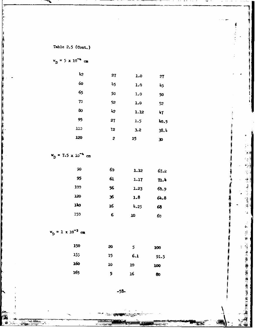
Table 2.5 (Cont.)
42 27 1.0 27
60 4e5 1.0 4.5
65 50 1.0 501
TO 52 1.0 52
8D 4.2 1.12 1.7
95 27 1.5 4.5.
1012 3.2 38.4.
102 15 3D
90 6D 1.12 6T.2
95 61 1.17 hIA
100 561.23 66.9
1036 1.8 64.8
14016 1..25 68
150 6 10 6o
v! l
150 20 5 lao
155 15 6.1 9.
160 10 10)10
165 5 16 8o

0 >I
o P
o 0
owwI E0
Ci)
00~
0c~g
w
-0 c
0 <~
HiO.3Vdl NOII1~fldiiflVW 3HONVIVAV 00cJ
-59-

M1
The effect of space charge9 ,5 1 on MA can be seen from Fig. 2.16.0
The upper limit on de collector current density is dependent on N andav
Ndrift. The electric field profile in a typical IlII-LO collector is
depicted in Fig. 2.17. As JTd increases while VT is held constant,Tde
E(W av) decreases. If the space-charge density is higher than Ndrift"
E(wT ) is higher than E(Wa). If N is very high, E(wa) at J = 0Sav av Eav T.
is low and it does not take a srace-charge density much higner than
N drif t to force E(w av) below Es. If Ndrift is very low, the electric
< <field in the region 0 = x = W decreases rapidly with increasing
j, while V, is held constant, therefore, MA decreases rapidly withdc A
increasing J. . Moreover, the sign of dE/dx is reversed at lower Jde d
which means that E(wT ) is higher Than E(wav). The condition th.t no
significant carrier multiplication occurs near x = wT is violated at
lower JTdc for devices with lower Ndrift. A situation could arise
where the collector region near x = 0 becomes undepleted before E(WT )
is sufficiently high to cause significant carrier generation. This
collecto-" current induced neutral region will effectively increase
the effective neutral base region width and the base transport factor
will decrease. This case is shown in Fig. 2.17 and corresponds to
Sd . The aforementioned space-charge effects have been demon-
strated by applying AVALAN on various collector structures at different
dc collector current densities.
2.1 Summary
This chapter contained the ionization rates of electrons and
holes in Si and GaAs and comparisons of the dc avalanche multiplication
factor vs. VT characteristics of n-type and p-type Si and n-type gaAs
CATT devices, n-type Si devices are found to have the most suitable
-6o-

E 0 000% 0 00N
IN. 0 '-i
10 0 N*- 0
C) > 4
<1 0
xx
(0
C)0 H
C13
I~ 0
9) 0:0 E-4m
0s IL-
x Ir
00
C0-
-6o1-
.~. - >
L0 ___

wLL J4
w
WW
Wov w T
DISTANCE
FIG. 2.17 DEPENDENCE OF THE ELECTRIC FIELD PROFILE ON
SPACE-CHARGE DENSITY, N AND Ndrift'
(o<J <J <J)1 2 3

Mvs. V1 0'~acteristicsfor making high-gain CATT amplifiers., The
effect of collector structural parameters, i.e., Nav N ditand wD
oi. M vs. V T characteristics,were investigated asid the effects of
te-mperature and space charge were discussed.
-63-

CHJAPTER TI. DEVICE PHYSICS, DC AND SMALL-SIGNAL ANALYTICAL MDE7!
3.l introduct ion
This charter tresents a discussion of the physics of CAtIr
dev-ces, a dc aalytc model and a small-signal one. For the dc
dev ice model, the analytical expression for the avalanche multiplication
factor, which wa derived in Chapter II, is employed in describing the
current nultir-lioation phenomenon. T!.e effects of hi7h-level
:n,'ectiol In trhe Lase reiion are ignored, but are included in the
large-signal simulation model presented in Chapter IV. The dc space-
ee..t -n. tne collector region are included. Te space-charge
effects are different under RF operating conditions and they are
considered In deta!l in Charter IV. .7he electric field in the
co'lector depletion region is assumed to be sufficient to sustain the
carr'er saturation velocity eveirwhere. a1e small-signal analytical
model n Ier'vo- cro a first-order T-;alor series expansio,. of dc
auamntbo' and eiuat'onz atout th'eir -uiescent values and the lineari-
zat r C t4.e re.-ltind e-uations. This procedure, in general, produces
cocpled rrnr nar ordUinary differential equations n phasor spice for
te small-simnal variable of interest: particle concentrations,
particle currents, terrnal voltages, etc. hne small-signal analytical
model does not only include the current multiplication phenomenon, but
also the transit -tme effect associated with the base-collector deple-
tion reiion. The common-base y-parameters are derived and the
unilateral power gain, maximum freqdency of oscillation, operating
power gain, transducer power gain, optimum source and load terminations,
-64.-
-- _ _ - ~ _ -

.ainvll sa ty factor, and bandwidth are calcuLated. A brief
sc-.ss Ion of the possibility of' operating CATT deviceo as IMPATi
diode. "th varia:,bl, equivalent thermally generated current I.; :iven.
% ~cAnal-tical *code!
:.2. Carrier Concentration in BJT and CAT71 Devices. The
Aard .; .-on for carrier concentrations and currents in th. field-
're ha.-z-- reion of a n iformly doped W3J T or CA77, structure u nder low-
levei in .ct io:: wa.n 1'rst presented by Shockiey 2 in the classic paper
..at Introduc-d the junetIon transistor in 1949. Shockley's transi:;tor
theor. sti'll ;.-rves as the foundation for all present-day theories of
_poiar .j'cntion transistor operation including high-level injection,
e~i'd-a Wed bane transport, the Webster effect and Kirk effects. A
one-d'mensionai uniformly doped npn structure is shown in Fi.I 3.1.
The rdinorlt.,V carrier bcundary conditions at the base edge of the
esitter-base depletion region and at the base edge of the base-colIector
deple:ton region first introduced by Shockley are
n(w ) = n exp (eV AIT) (3.1)2 o
and
n,w ) n exp (- eV /kT)
r..:e y-e y, under normal bia:s conditions, where V is the emitter-
ba:se termina! voltage and n is the thermal equilibrium concentration.o
A,_tnication of these ex,,res.ions for the minority carrier boundai-z
conditions to MiT and CAT device:; with the emitter-base unction
for-tard biased such that n(w ) > o, the collector-base junction2
reverse 1iased saCh that n(w ) << n, and with a base width greater tha&n3 o
-65-
_-

0
0-i-IL z
000
if) 'C
OD 0 U)-~r)
lAcr
0 CL '-4)
COW W0c<t
~0w 5
wo
-66-
-- - -_ _- - --_ _ - _ -

several Debye lengths52 yields a satisfactory description of carrier
transport in the base region under low-level injection. The modifica-
tion required in Eq. 3.1 under high-level injection is discussed in
Chapter IV. If the boundary condition required for the analysis of the
collector region is the minority carrier current density, Eqs. 3.1 and
3.2 are adequa4 -. If the collector boundary condition required is the
minority carrier density, Eq. 3.2 is not appropriate. The requirement
that the minority carrier concentration at the base edge of the base-
collector depletion region be less than the thermal equilibrium
concentration, independent of the minority carrier current density,
is disconcerting at best. An expression for the minority carrier
concentration at the base edge of the base-collector depletion region,
which would result in a smooth trawition from diffusion transport to
drift transport that the electrons must umdergo in traversing the field-
free base region to the high-field base-collector de. tion region, is
given in Chapter IV. For the dc and small-signal analytical models,
the collector boundary condition required is the minority carrier
current density. The case where the base width becomes comparable to
a Debye length has been investigated by MCleer,5 2 but it
is of no concern in the modeling of CATT devices.
If a constant base-doping concentration and a low-level emitter
injection are assumed, transport of minority carriers in the field-
free base region can be described by diffusion alone and the dc
electron current density is
dndc
Jd -- eD dc (3.3)
Jn dc eDn dy "31.3
-67-
N - - -

where nde is the dc electron concentration and Dn *5 Uh lt-field
electron dif'fsion constant. nother relations-ip 'ch goiverns the
base rxeton electron distr'bution is the tim-inden~nat electron
contInu.ty equation
dJni n n
= do 0 1 dce dn
ren electron lifetime. By sustitut-Ig Eq. 3.3 into Eq. 3.1,
n ocencent. ordinary differential
a~Y"2 I-,- co--an coficet iswAeQuat: + baine whos solution is of the form:
.- (y-w )L(- In-'y% 2 n + n=_-
where L = T = the electron difflusion length in the base reg'on.n n n
'The constants A and B can be determined frm *-he b-omdary conditions
given by Eqs. 3.1 and 3.2. Once nde(y) is found, the electron carrier
current iLs determined from Eq. 3.3. At y w and w , the do electron2 3
currein ts are
eD A_ _in-" n L dc ct
ndc L
a.
ad
-68-

AiAi
T (w) in F 2 - n cB'nn3 n -dc dc 2 o
n) c~lothi. (3.6)
w-ere A. is the tter areaw_ - w
f2c D '-'
L 1 + w
2 !enIJ ' I -,
B 0i
0
doping levels, VF,~i the de em' tter-bne terina voltage -and V i
_u e s ter l (3.8)i
0the built-in potential at the proper 'unction. Under normnal bias
cfolowing i bained:
.-In w nL coh 7- (3.9)
anid
n z-n ac -n cshs7j1(.0
nB dceC i (.0
The hole current crossing each Junction must be calculated in order to
find the total current. Unlidth, - D lectran current which links both
emitter and collector Junctions, tt'e hole currents link only one
Junction because the base hole current, can easily enter or leave
-69-
F -- ,_ _ _ _ _ _ _ _ _ _-\ L

the base region owing to the ohmic contact to the external terminal.
The dc hole current at y = - vi can be found from Eq. 3.5 by changing
all the electron parameters to the corresponding hole parameters in the
appropriate regions and by taking the limit of the resulting expression
in the limit as vB - -. The result is
_v pA= I (-it) = Te P[p V e(-v o (3.U) i
pEd Pdc 11p - 0
where D = the low-field hole diffusion constant, L = the hole diffusionp p
length, P = the hole thermal equilibrium concentration, and
V
S1/22c N'A ____
w = (3.12)H1A "BI VEB 3)
0
The total dc emitter particle current is given by
fn (v) n coth~tj~ f d.. ) PTV ~L Idc 2 P,(-, odc
If B << L Eq. 3.133 can be further reduced to
- n (V)nJA fp,- [p€- p) ] . (3.4)dc 1~ dc 2 n Lp
A very important circuit parameter is the short-circuit dc
current gain from emitter to collector and it can be written as the
product of three parameters as follows:
-70

0 do = f- Td (3.15)de 'Edc ( Jdc InBdc
The first factor is the injection efficiency aj which gives the
fraction of the total emitter current which is made up of the electron
carriers. Under normal bias conditions, the do injection efficiency can
be calculated by the follating expression:
1ij ( (3.16)
n p n)
The second factor is the base transport factor which is given by the
foiiowIng expression:
M = seth .(3.17)
The most accurate two-term expression for a ist i
0 d (3.18)0 n!
T.e third factor is the collector avalanche multiplication factor. For
BlfTs' It Is essentially equal to unity. Fcr CATT devices, it is given
by Eq. 2.7. For convenience, Eq. 2.7 is stated again as follows:
I - J T jexp J [ap') -n0 0
A-
- -T - -
_ _ _ _ _ _ _ _ _ _ _

A good microwave B-' or CATT must, first of al, be a good de
BJT or CA.-'. From the expressions for a and ato tle designin,)
0 0requirements on the emitter and base regions can be deduced.
B3.2.2 ase Spreading Reistance. The cross section of a singe- .-
emitter strin in an interdigitated device structure is shown in Fig. 3.2.
The base spreading resistance can be calculated by using the follovi rg
e ~ e s On 5 3
_( w .d 1
2 LaB 2 oZtJ nuder of e~Jtter-base fl r ars
1 2(3.19)
where the device structiwal parameters are defined in ig. 3.2 and the
coductivity of the umifor-ly doped base a3 is
0 M epii.
The varation in F. due to base region conductivity nodlation, whi-di
is caused by high concentrations of electron and hole carriers at =
mdic or high-level injection, and base region wit mod-al ati
whi c h s caused by the Early effect, 3 has been ignored in the device
meelr g.
3.2.3 Dc Co aer .Model. The computer model is snown in
Kig. 3. 3a. The zarticle current L. liming in the dioe is given by
Eq. 3.13. The collec-tor rL-ticle curent is calculat-d by--dc
su-prlIn input data i V,, and device structura v u ters toI
4C othe conuter program D , w ere given by . 0i=. cen
avalanche mtinlica4 u occurs in the- I coflrtr deneto reg-on,
-72-
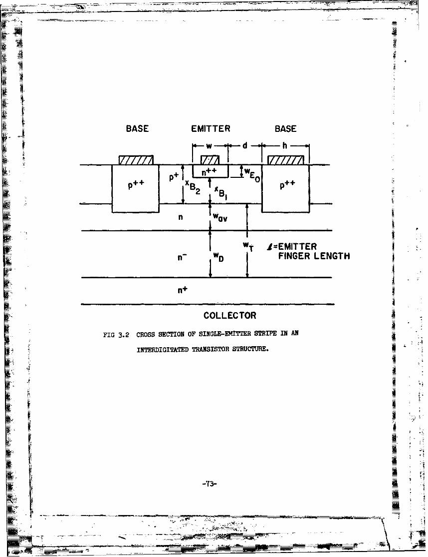
BASE EMITTER BASE
t AT 77MITE
= FIG 3. CROSS ECTION O SINGLEEMITTER SRP NA
INTERDIGITATED TRANSISTOR STRUCTRE

EMirTt* COLLECTOR
to)
-T"
__ ww wl. %W.va
FIG. 3.3 CALCULATION OF COMWIN-BASE COLLECTOR CHARCTERISTICS. (a) -
DC DEUICE MODEL AND (b) BLOCK DIAGRAM OF DC PROGRAM DCCP.
_ _ _ _ _ _ _ _ _ _ _ __ _ _ _ _ _ _ _ _ _ _ _ _ _ _ A -

electron-hole pairs are created.- Electrons, emitter injected and
avalanche created, will drift toward the collector contact. Holes,
mainly avalanche created, will be transported into the base region and
therefore constitute a negative recombination current component.2 8,54
They reduce the base current which must be supplied externally. If
the avalanche multiplication factor is large enough, the polarity of
the base current actually reverses because the avalanche multiplication
process in the collector depletion region is providing more holes to
the base than are necessary to support recombination in the base and
emitter.
'The common-base configuration is chosen because the consequences
of this avalanche multiplication are straightforward in such an
operation. The collector particle current simply equals the product
of I and M Current is the parameter of the coumon-base
collector characteristics and it is dependent only on VEB, the de0
emitter-base terminal voltage. Therefore the comon-base characteristics
reflect primarily a direct avalanche contribution to the collector
current. The consequences of avalanche multiplication are more
complicated and subtle when the transistor is operating in the comon-
emitter configuration since base current IB is the parameter of thedc
collector characteristics. The avalanche multiplication factor is
dependent on VT, Id and ITdc are dependent on In and A and0 e dc de 0
IB is the difference between the VEB -dependent recombination currentIdc0
and I Therefore, points on n Id vs. V (constant IBdcpBdo Tde T0 doAC
characteristic curve may correspond to different values of I andnilde
such a characteristic curve does not reflect directly the avalanche
contribution to the collector current.
-75-• 1%

Figure 3.3b shows the block diagram of the computer program DCCP
which produces the common-base dc collector characteristics. The results
of computer program DCCP are given and discussed in Section 3.4.
3.3 Small-Sigja Analytical Model
To consider the general ac case, the general one-dimensional time-
dependent electron continuity equation must be solved:
aJ n -n
n
The following is obtained using Eqs. 3.3 and 3.20
S-L(n-n) 1 n '3.21)T2 o D atn
and the solution of Bq. 3.21 is of the folowing form:
n(y,t) = ndc) n yett (3.22)
I
when the sources are sinus-oidal with frequency . The first term on
the right-hand side corresponds to the dc solution. The second term
.s the ac variation and is in the form of a product of two ter. TIs
is a frequently used method of solving partiai differential equations.
vt is assumed in &, 3.22 that the minority carrier concentration -vriesIS ass da ihn 3.422n that hes.
sinusoidally with e same frequency as that of the driving sources.
When Eq. 3.22 issutstituted into EQ. 32.21, the foflowin4, to esuations
are obtained:
dic dec -Vi(3-23).2 L
1n
-76-

-arid
_. = 0 . (3.24)
-e boundary condi fan in Eq. 3 qui'e general and is not restricted
to dc apied vtares. T us i" t--e etter-base Junction voltage is
eomosedat' a dd voltageV. and an ac voltage Vo a c t the minority
0 1carrier concentration on- the base side of the e-itteer-base lunction is
VEB U. v/kT eV_
.. tw nt. Li 1IC 3.25'
whre the first term on the ribzht-hand side is the dc value and the
second term is te ao value. Equation 3.25 is valid provided that
Iv p A.." - (3.26)
w"'-h renresents the small-signal assuption.
Note that the f o- of the d!e rential equation for the aceetron density in Eq. 3.2h is the same as tat for the do electron
density.* This sugge_;ts that the a z solution can be obtained from the
aa solution directl by the use of so simple transfomations. The ac
electron part-icle currents at y = w and v are found to be
e D A (I+ JWT ei 4 n
-jwt -nB +1ndo 2 -iLe - T: L )n (w coth L
n I n
(3.27)
an d
-TI-

-~ k2 JT n E ejm t !w j Tn
Ie L e n i n (w2 csch LI nn
(3.28)
under normal bias conditions. The depletion region boundaries w and2
v are determined by Eqs. 3.7 and 3.8 ith V and VT set at their3
respective de values. The hole current at y - is given by1
ejWt 1+JIp e
1pE e - e A L VT $4 ) " (3.29)I p I
Physically, InB ej t is the time-dependent electron current injected1
into the base-collector depletion region. 7he expressions which
approximate the physics in the collector region under small-signal
conditions are derived next. Finally, the small-signal y-parameters
= of the camei-base configuration are derived.
Most of the carrier generation due to avalanche multiplication
occurs in a narrov high-field portion of the collector region, which is
nemed the generation region, whose width is v The remainder of the
collector region is the drift region whose width is v. . The basic
device equations in the generation region are
E = - ((33
ax C ND1 "A+ P n)- -1 p-l ,(3.3o)
J = evn , (3.31)n 5
J evp , (3.32)p s5
+ - i tav (n + p) (333)at e x s
and
-78-
- \ -ri- -
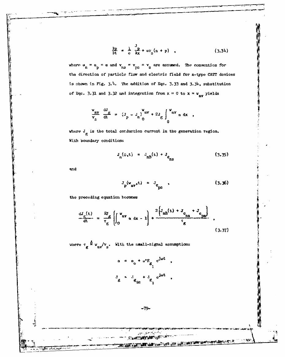
at e 3x +svn ) (3.34)
where a n a P aand v ns=v P- V 3are assumed. The convention for
the direction of particle flow and electric field for n-type CATT devices
is shon in Fig. 3.4. The addition of Eqs. 3.33 and 3.314, substitution
of Eqs. 3.31 and 3.32 and integrztion from x 0 to x v w yields
av dJ f= v+ 1a
v~ dt p n 0 2g avad
0
where J is the total corduction current in the generation region.9
With bDoundar7 conditions
j (Olt) =ja(t) +J1 (3-35)
nnd
J (V avt) ' C 3.6
the preceding equation becomaes
d~jt ( 2J.(t) +J iw~fav d, 1
g ~0 g(3-3T)
AWhere a 9 v /v s With the smaU--signal assumptions
gE av +sV
cx cx +' j et98
-T9-

DEVICE COLLECTOR JT(t)
STRUCTUREVTtO
CC Jcc
(a)
-'I
Vp
Rat - vn
I*LJ
C(b)
(b)ELMCFIMAN(b)M
-8D-

S= E + E ejg 9 g
JnB = _ + eAt
-dc 1
the followring can be obtained from -q. 3.37
+j +4= c X,. P (3.38)
ad iJav dx
0
the dewquation, and
4 - " c 1O.. ,x : (3.r)1
o 2
the no equation, where the second-and higher-order terms are neglected.
If the collector has a Read-typie stru-cture and negligible space-charge
effect, oth v and R. are constants. Equation 3.3 becomes£
f b g -) Eg +J = (3.4=0)9 WT
0
where N. -- i/(i - ao ). By using the analytical expression for the
o ar0
ionization rate
-b/Ego
i 0a = Ae
%I C _ __e

Eq. 3.40 can be written as
i9S - ( _r[v A)- lnlv( +j~ +j Ma i E +d b S+
0
(3.41)
Eqution 3.4l gives the current density at the interface between the
generation region and the drift region.
If a saturated drift velocity v and zero carrier generation in
the drift region are ass med, the ac conduction current densityJ Cx) e in the drift region propagates as an imattenuated wave at
I I
ti s d rift v e lo city W x- V
JD0 (x) = je ~ a (3.42)where the exponential tern represents the phase delay. The induced
ac collector terminal current dsity Is
° 11 v :3
sin -(O /2)ji 2 e (3.43)
2
vim, O wD1'Ts and Jt) J + J,T
iget-

The voltage across the base-collector terminal is VT = V +T
VT ej wt , where VT is the ac voltage component. The ae electric field
is constant throughout the collector region if the space-charge effects
of J and J are ignored (see Fig. 3.5). The ac electric field in
t e generation region is
VT
E .(344)- g vT1 WT
By combining Eqs. 3.4l, 3.43 and 3.4, the foliowing expression for
IT can be derived:
deoJC4MA - [tA T
I A
+ As(ODI2)AMA 2
00
Te preceding expression is a ore coqpete description of The sall-
signal device physics than The orlation of Winsey and Carroll
ad iis very siilar to The expression derived by Q(3-45
except That is a ssord to be infinity in the latter case. The total
0
c collector terminal current is given by
I = IT + JCV , (3.46)C c c TEw
where C f c V. The smali-siganal device model is giv en in Fig. 3.6ac
and the sail1-signal circuit model is given in Fig. 3.6b. The circuit
83-
L ________ _

~nJ
COLLECTOR
v Aw o vT V A
0 T
w
DISTANCE
FIG. 3.5 N~emc FYfl PRFITs JuLC R? caomocS.

1T1 2
Vb 4
CTE B2
EF TYin Yout
(b)
FI.3.6 SMALLSIGNAL moDELs. (a) DEVICE MODEL
AND (b) CIRCUIT MODEL.
-85-

element C is the emitter-base transition region capacitance and itsT TE
value is
ScAEI
where w and w are calculated by using Eqs. 3.7 and 3.12. If I and1 21
I , the total ac emitter current and the total ac collector current, are2
written as
1 a + Y12V b (3.48)
and
I =y V + y V ,(3.149)2 1 a 2 2 b
where 1I,1 and V 12are ac voltages across the terminals, then using
Eqs. 3.27 through 3.29 and Eqs. 3.145 and 3.46 yields the following
expressions:
I A+ JwT tanh (w/L)[ y _ _11 tanh [lB nWT Pdc 3 P +(3T(.0
y 0 ,(3.51)12
I nE 4 c nl sin -~ 2e dc no -D
21 BT Dv
sinh~ L 2L MA 2
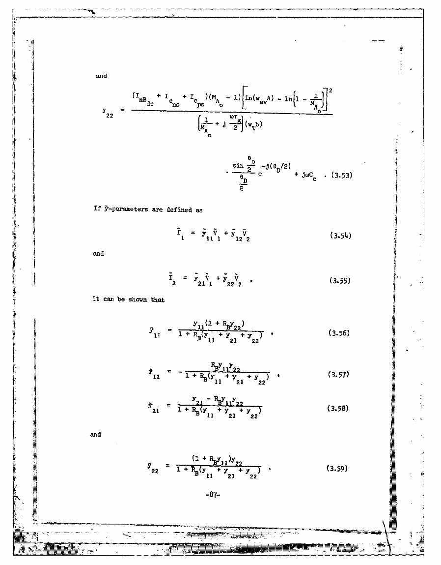
and
22
If~i-armtdcax dfned as 0
and-Iy
22 (i WTy2IM (3.56
2+ 1+~ (3-53)+
and
y( + y V2(3552 1 1 22 (
22 l+iR(+ y + Y T(6
~11 21 22

The input and output admittances, expressed In terms of j , are
Y. = G JB. = -12 21 (.0Y nG i n B i n "1 Y 22 + L(.0
and
Y G + JB 12 (3.61out out out 22 y + Y 3.1
where Y and YS are the load and the source admittances, respectively.L S
By using the derived k-parameters, many small-signal device performance
capabilities can be calculated.
I: The passivity condition5 5 is given as follows:
~0 (3.62)
92 2 0(3.63)
I~ +,~12S+ 621 12 0 (3.65)
91122 1221
-U =0
where

UI? -21 12ft=- _ ) -(3.66)t 22 - 12 921
> <Thu, if g = 0 and =U =1, the device is passive. If11 22
U > i, the device is active. The quantity U is a measure of the degree
of activity. 'The maximum frequency of oscillation wm is defined as
S( = 1 . (3.67)
The Linvill stability factor Siz5 5
s -- 2gg -- " + (3.68)11 22 12 21 12 21
When 1 < S < or when S < O, the device is potentially unstable, that
is, oscillation can occur for certain selected passive terminations.
When 0 < S < 1, the device is inherently stable, that is, no passive
terminations can cause oscillation without suitable external feedback.
When S = 1, the device is critically stable (see Fig. 3.7 for the
definitions of various powers). The operating power gain is
out 0.-I'- , (3.69)in ' +2 Ref12 + 1
22
where Re is the real part of any complex number and G = Re(YL) IfL L
the amplifier is inherently stable, the maximum operating gain is
achieved when the load is
4 V'2ft t -Re(y y ]2 -j 2 (.0
Sopt 7 11 22 1221 1 21
-89-
I -- - --.. .---- - - --- . ..-- -- 7- - - ---
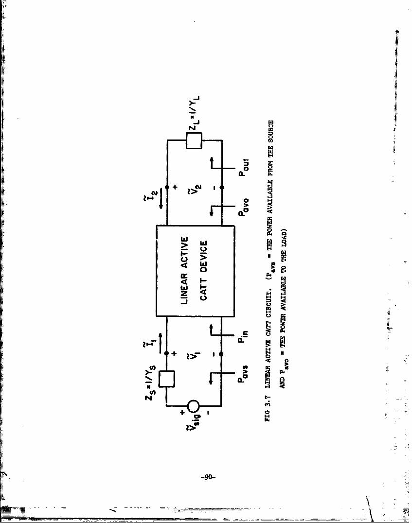
II
-J
N.N-I
N C)Liz:20CD
r4
4-
00. rz.
+ N0
0
I-
1~>111I-
C)> U
Pd41-w I-z 4 E4~
- ___ HC
0~~zs-~1 +
0) 0'I
N. £L0~N0)
N
+ 3 0'-4r~.0
-90-
-- -:~--~t-- ~ -- = - - - -

t1-
I=
and
B (3. U)Lot 29 22
where Im is the imaginary part of any complex number. Substitution of
Eqs. 3.70 and 3.71 into Eq. 3.60 yields the input admittance Y. with
Y = YL .In order to deliver maximum power to the device the input
| optadmittance must be the conjugate of the source admittance; therefore,
when Y is given byt S
GS = Re(Y) -21t A Re(9 y )j2. t 12opt 22 112242 12 21 12 21ot22
(3.72)
and
B = 6 ,(3.73)"S 2R iopt 22
maximum power as well as maximum operating power gain are achieved.
The optimum terminations for a CATT amplifier are usually obtained
by adjusting the values of the components in the matching networks.
Ease of tunability, or alignability, depends on fractional change in
input admittance compared to the fractional change in load admittance
and on the fractional change in output admittance compared to the
fractional change in source admittance. When the fractional changes in
input and output admittances are small, it is not necessary to alternate
many times between input and output tuning to achieve the desired
condition of operation. In terms of the Y-parameters, the input
-91-
Mu_ _ _ _ _ _imp

tunability is given by
6 = dYL/YL - 1Y2 2 + YLI t (22 + - (3.74)
Tuning is easier as 6 is made smaUer. In order to achieve goot
tunability, the load admittance may be chosen such that YL > in
order to make 6 < 0.3. Then Eq. 3.74 becomes
6 -- • 21 (3.75)"11 L'
The output power varies with frequency partly because the device
parameters are frequency dependent but primarily because the conditions
for a conjugate match at the input and output ports may not be obtained
except at the design-center frequency f . The amplifier bandwidth can0
be approximated under certain conditions from the inherent bandwidth
BWi at either port given by5 5
2fog
opt
for the input circuit, and by
2f GoL
BW~ut =ii7-2rTopt
for the output circuit. Inherent bandwidth is the name given to the
bandwidth that is obtained in the conjugate matching situation where
the optimum terminations are determined only by the device parameters.
It often happens that >> B W and in such cases the overallin out
-92-

amplifier bandwidth is determined by the output circuit. Bandwidths
are inversely proportional to B, and BS. Therefore, the input or output
bandwidth can be decreased below the inherent bandwidth by adding shunt
capacitances C_ or C across the input and output terminals without
affecting the optimum termination conductances. Maximum operating
power gain is still achieved. 'When an inherent bandwidth is too small
for a particular application, the bandwidth can be increased by raising
the termination conductances. T1his means that additional shunt resistance
can be connected across the input or output terminals. The power gain
is decreased when the bandwidth is increased.
When the transistor parameters are such that potential instability
occurs, a certain output load causes the input conductance to be zero
or negative and the power gain to be infinite. A mismatching technique
can be used to ensure the stability of the amplifier circuitry.
3.4 Dc and Small-Signal Results
Typical common-base characteristics of CATT devices are shown in
Figs. 3.8 through 3.10. Carrier multiplication is evident from the
common-base characteristics. Figures 3.8 through 3.10 represent three
CAT devices with different doping densities in the avalanche multipli-
cation region. The effects of N are observed in the different ratesav
of increase in J as a function of VT , different breakdown voltages
and different punch-through voltages. The effects of Wv, N andav driftFV D on the common-base characteristics can also be investigated by
applying the computer program DCCP.
It can be inferred from Figs. 3.8 through 3.10 that coninon-base
biased CATT devices can be employed to product current amplification,
and the device in Fig. 3.8 is suitable for such applications. The dc
-93-
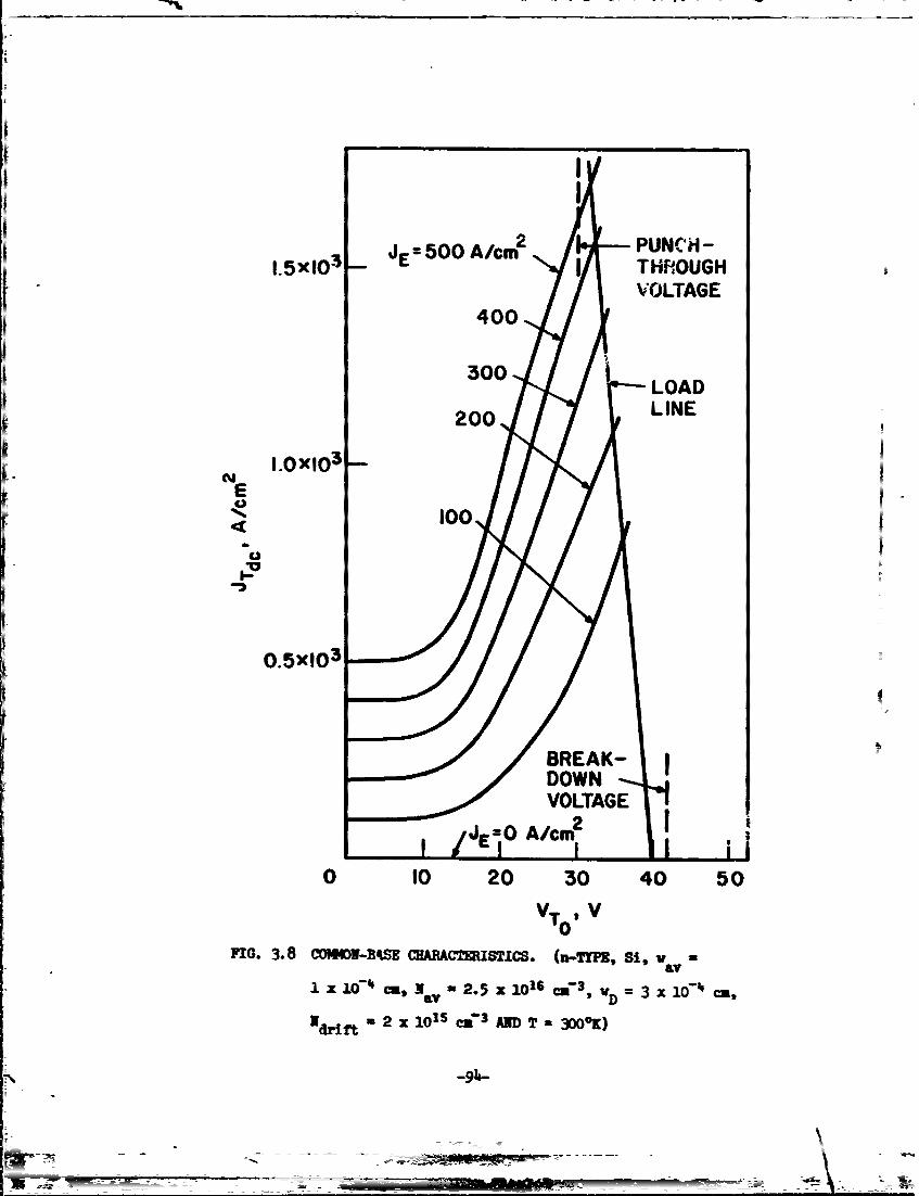
2E50Ac PUNCH-L-5xI03 - E 0 Ac THROUGH
VOLTAGE400-
300 LOAD
200 LINE
E100
FY
0 10 2E0 30 40 5
VT V
FIG. 3.8 coWMN-BM QCUMCS'flcs. (n-T!T', si, v =v
.1 x1074 Co. N ay=2.5 x101 6 coi3 .VD 3 x 1074ca,
ldr~r -2 x 10¹⁵ -3 AND T 3D00K)

JE5 0 0 A/cm2
400
LOAD LINE30
PUNCH-
ERAKDOWVOLAG
42UJ7
/m
0g0P 3 05 6 08
ay a
wD 3x 10⁴ c, X~ft 2x 10¹⁵ ~jI
AND T 3009I
_95-

1.5x10 3 JC0 nAc2
LOAD LINE400
300
t~xIO3 PUNCH-20
VOLTAGE I6
C 100
-) BREAK-DOWNVOLTAGE
0 50 20 30 40 50 60 T0
VT.V
FIG. 3.10 CCIIIN-BAS CAATU C5. (ni-flf, Si,
vav=1 x 10⁻⁴ca.N av=2 x101 csr3 ,
VD = 3 x lra, Na t '2zx10 1 5 ojr 3
AND T! 3000K)

=*
base-collector bias should be set close to the breakdown voltage as
long as the thera- limitation is not exceeded -and the load resistor
is small (see Fig. 3.8). For applications in voltage amplifications,
the device in Fig. 3.9 is more suitable. In fact, a device with a
lightly doped, uniform collector structure has even greater capability
for voltage amplification. The dc base-collector bias should be set
close to the breakdown voltage in Class C operation and set close to
(lI)(VIB + V I in Class A operation. The upper and lower limits of
V are VB and Vr, respectively. it is assumed that a punched-through
or nearly punche -through collector is a required operating condition.The load resistor is large. For applications in power amlification,
the device in Fig. 3.10 is rore suitable where both a large current
miultiplication and large VF can result with proper dc bias and load
resistor applied.
A computer program SW? was written which is capable of
determining the small-signal corion-base y-parameters of CT? amplifiers.
Typical U vs. frequency and maximum operating power gain vs. frequency
plots are shown in Figs. 3.11 through 3.14. The quantity U is plotted
over the frequency range in which U = 0. Note that the device can still
be active even if U < 0 as long as either g cOor g <0. VAximm11 22
operating p oer gain is displayed cver the entire frequency range in which.
the device is capable of power amplification.
r Fis. 3.11 through 3.1 it is observed that the maximum
operating per gain at I > is muc lower thanthe maximum operating
power man at M , but the gain at M > I is constant over a very
wi ea o ftequncie. Tf 7r < 0.8 V, avaDnche multiplication0
wil imreae a the maximum frequency at which an operating power
-97-
0777-"- IZ ~

0 C0
0 to
0 0 00 0 00w 0
0 2 r
0 0& 0
OP~OI gNV K~

V0
0v
- z
w0 10
All -w
0
I OD
1100
0I0 0z00 0
In'
E-4
CD"
0
0 0 0 0 0 0 0 0- C
SP 'NIVS 83MOd
-99-
57 T z~a

0 0 V 0 -
If 0010 - P
0 L
000 0 0 0 0 0-Q~ D In) v ) C~
=100

co
0 ~ ~ 0 0 00 C
0V Oo
2w
3 0
SP4 IS 3~

gain greater than unity occurs. From Figs. 3.11 and 3.12 it is
observed that at frequencies higher than f," avalanche multiplication
also increases the operating power gain. IF V > 0.85 V, fEB max0
decreases with increasing MA and the operating power gain at M > 1A A0 0
is smaller than the operating power gain at M = 1 throughout the entireA
active frequency range. The effects of V on f and the operatingVEB max0
power gain are illustrated in Fig. 3.15. Highest f at MA = 5 isA
0achieved when V = 0.7 V. Highest operating power gain at MA 5 isEB A -0 0achieved when V = 0.8 V. When V = 0.7 V, f is severely limitedEB EB maxo 0 >by a large value of the emitter space-charge resistance. When V =
EB0
0.85 V, f..x and operating power gain are reduced due to large values of
Jn From Eq. 3.45, there are two components in J . One componentdc 1
represents the carriers contained in JnB undergoing constant avalanche1
multiplication which is determined by V . The second component, whichT
0is
(dn-d Jcn + jc MAOlBJ(av Aml i3[rdc z cps
+ j (bwT)
eD
sin - -J(eD/2)_D e VT
2
represents the carriers corresponding to JnBdc + J + J undergoingCns Cpsnoneonstant avalanche multiplication which depends on the instantaneous
voltage VT VT + VT e t . The second current component is
0 1responsible for the decreases in f and the operating power gain as
-102- V _ _ _ _ _ _ _ __

I7
70-
z0-
0 0.
I. 30 MAX5U O0R*N6OWRGI S.FEUNY(VT/0. =~1~u10.6
wI
-103
.90.9____

14A increases. If the second current component is artificially forced0to vanish, the corresponding maximum operating power gain and U are
displayed in Figs. 3.16 and 3.17. Note that the power gain and fmax
at M = x are always less or equal to operating power gain and fA max
at MA y, if x < y. Figure 3.18 shows that for a given value of MAo o
higher V , up to 0.8 V, implies higher f and higher operating powerEB max
gain. For V > 0.8 V, maximum operating power gain coincides withEB0
that corresponding to VE = 0.8 V. Comparison of previous results and0
the results obtained by artificially setting the second current component
to zero indicates that, for the most part, avalanche multiplication of
carriers in CATT amplifiers, when operating in Class A, works toward
reducing the operating power gain. The situation is that the value of
V must not be too small, otherwise, the emitter space-charge resistanceEB
0will severely reduce f and the operating power gain, and if the value
max
of V E is large, the second current component will dominate which has0
been shown to degrade the operating power gain. From the expression
for IT the phase difference between VT and the second current component
equals (e,/2) + tanl(wr gMA /2). If - v/2 < phase difference < w/2, energy0
is being dissipated. The situation in Class A operation at low frequency
is depicted in Fig. 3.19. It is assumed that the load is a high-Q
tank circuit whose resonant frequency equals the emitter-base input
signal frequency. Notice that the amplitude of the first current
component, when VT is large, is less than the value given by Eq. 3.45.I
The reason for this is that when nB is maximum, V_ is minimum and the! nB s T
carrier multiplication is at its minimum. When nB is minimum, V.,I
is maximum and the carrier nzitinlication is at its maximWu. This
-10- i

00
0i 0
0-
0 4 0-~
-0 o
0w0 0 0 0 0 0 05 raC
0~~ ~ ~ 00
-1050
ON 0 0

=0l0
02 000
4
0
0 0
0
00
=0
-1060

'0 o\///0
8P I-I£4 I
f40,
1-4
011
0Z
o £4CD)
o
00
0 0 0 0 0 0 0 -0 0 0 .
> 0
0 0
00
owwM
0too o~ on 0 0E 0% 0-
8P 6NIVO 83MOd
-OT-

no~d
VT
T,-T
z MA IS DEPENDENTo ONVT0 T00
0 -A I DEPENDENTU) 0 ON VTU.
zwiz0
L
00z
V) PHASE
FIG. 3.19 SCIEKATIC PLOTS OF JnB V T FIhST COMP~ONENT OF
J , AND SECOND O14ONEN-T OF JT
-108-

situation can be seen by following the load line in Fig. 3.10. From
the phase relationship between VT and the second current component,I
it is clear that the second current component corresponds to energy
dissipation, therefore, it reduces the operating power gain. The
usefulness of carrier multiplication and long transit region can be
rep! zed only in Class C operation, assuming a proper load is applied
acros~s the base-collector terminal and the width of the charge pulses mu~eh less than ; rad. -e Class C operation of CAWT amplifiers
was yriefly described in Chapter i and the large-signal simulation
esttlfts are discussed in detail in Chapter IV.
OTneration of a CAM as an UATT with Variable Ecuivalent Therma1ly
Generated Current
There has been considerable interest in the operation of an
TDU2T diode with an externally controllable equivalent thermally
generated current. Sanderson and Jordan5 6 discussed the operation of
an IMA-OAT acted upon by an electron beam. The electron-beam-produced
current is subject to multiplication in the same way as the flow of
actually thermally generated carriers. The sm of the electron-beam-
produced current and the current due to thermally generated carriers is,
by definition, the equivalent thermally generated current. Sanderson
and Jordan derived small-signal TDhATT expressions which theoretically
predict that an appreciable change in the IMPAT resonant frequency
can be induiced by varying the electron-beam intensity. Results suggest
that frequency modulation of the IMPAIT oscillator can be implemented
by this method. Forrest and Seeds 5 7 and others have studied the
controlling of microwave MATT oscillators with an optical signal.~~-109-
_____ =-0-
- r
A -

The use of an electron beam or an optical signal on an IMPATT
is equivalent to the situation where the base collector of a CATT is
operated as an IMPATT where the emitter and base simply act as an
externally controlled thermal current source. The expressions derived
by Sanderson and Jordan can simply be obtained from Eqs. 3.3T by
allowing M * end J (t) JA nB nBo dc
3.6 Conclusions
In this chapter analytical expressions required for dc and ac
small-signal CATT device models have been derived. A simple computer
program, DCCP, has been written which can generate the common-base
characteristics of various CATT devices at min'ual cost. Another
computer program, SSCP, has been developed which can find the device
small-signal y-parameters, unilateral gain, maximum operating power gain,
optimum load, inherent input and output bandwidth, Linvill stability
factor, amplifier tunability, and the maximum frequency of oscillation.
The output results of SSCP indicate that under certain restricted
operating conditions f increases with increasing MA and the i
operating power gain at MA > 1 is higher than the operating power gain0
at MA = 1 for frequencies higher than a critical value f . However,A x
0
for frequencies lower than f , the operating power gain at MA = 1 isx
0alurys much higher than the -operating power gain at MA > 1. The cause
0for the gain reduction was determined to be the component of J, due
~1to V1 T, -dependent multiplication of those carriers correspouding to Jndc
This component of JT represents energy dissipation. Ccputati al
results of SSCP and DCCP indicate that Class A operation is not very
suitable for CATT amplifiers.
-no-
-110-

CHAPTER IV. LARGE-SIGNAL COMPUTE MODEL
4..1 IntroductionIn this chapter a large-signal computer simulatic is developed
which is hybrid in the sense that the emitter and base regions are
rodeled by lumped, nonlinear and tir-varying circuit elements whose
values are determined by a set of analytical expressions while the
collector region is modeled by employing the difference-equations
version of the semiconductor differential equations. The ana yti-al
expressions for the circuit elements of the lumped-cIrcuit model for
the emitter and base regions ar derived. "he ntmerical methods used
to solve the difference equations are modified version- of techniqes
which have evolved in the Electron Physics Laboratory in the past
decade.58 -6 2 Detailed descriptions of the numerical algorithm,
computer programs, and computer output are also given.
4.2 Develouent of Device Simulation
4.2.i General Description. Figure 2.1 shovs the depletion
regions of a normally biased CAT? device and its circult zdC 4s shown
in Fig. 4.1. The eitter-base region of the CAT device la represented
by three nonlinear circuit elements similar to those in Dfls: a diode
in which the particle current is injected across the fornr@-biased
emitter-base Junction "whose magnitude depends on the emitter-base
Junction voltage V ,a V ZJ-dependent depletion capacitance C
and a V -dpnetdiffusion capacitance Resistor P, Is the
equivalent base region spreading resistance. ?he collector region is A
represented by a c.ancitor C and a dependent current source I. The
-11--

Vbios
1E
Vsig cc CC
+ - VEB +RBV
-1~\_Vbias
FIG. h. aJI W)Icur M FOR A CAW? AWBLMMl IN TE
CW6631-EL5 CEOFIGUATICO.

capacitor Cc is the collector depletion capacitance and the dependent
current source IT represents the induced current whose value depends
on the amount of charge injected into the depleted collector regicn from
the neutral base region and the magnitude of carrier multiplication. It
is assumed that the drift region is always completely or nearly
completely depleted. Otherwise a VT-dependent resistor must be added
in series with the collector circuit representation depicted in Fig. 4.1.
The remainder of this section is devoted to detailed derivation and
physical interpretation of each element of the device model.
4.2.2 Emitter-Base Circuit Model and Computer Program EBCP.
In the bulk of the base region, the space-charge neutrality condition
always holds. Thus in the base region of n-type CATT devices,
n(y) + NA(Y) - p(y) = 0 . (4.1)
An important observation about current in n-type CATT devices is that
there is a negligible flow of holes (majority carriers) in most of the
base region between the emitter-base and base-collector metallurgical
junctions in the reverse direction. This is true under all bias
conditions because there can be only a vanishingly small flow of holes
from either n-region. The following expressions cali be written for
hole current in the longitudinal dimension y and the electric field:
J 0 epE(y)- eD dy
II
and
E(y) = kT 1~
e p dy '(4.2)
-113- IM

where p, the concentration of holes in the bulk base region, is related
to n and NA through Eq. 4.1. In a uniformly doped base region, the
electric field is negligible at low injection levels, that is, when the
concentration of minority carriers is much lower than the base region
impurity doping concentration. Therefore, the emitter-base junction
voltage VEBi equals the emitter-base terminal voltage VEB. At high
injection levels, the electron concentration is significantly higher
than its thermal equilibrium concentration and the electric field in the
bulk base region can no longer be ignored. A portion of the emitter-
base terminal voltage appears across the neutral base region such that
V .is less than VEBj EB
w
V EBJ V EB E(y) dy
2
By substituting the expression in Eq. 4.2 into the preceding relation,
V can be expressed as follows:EBj
k T (n p ( w ) ' 1% .3V- - ~- -,- -EB e tA
By using Eq. 4.3; the charge neutrality condition at y = w ; and the2
junction law, n(w) = n (w ) exp (eVEBj/k-), the following expression2 0 2 B
for V EBJ is derived:
[I / 4n? exp (eV /kTRB V Lnt NT JJ + -114.4)
where n. is the intrinsic carrier concentration. In order to be1
-111-

assured that Eq. 4.4 is valid at any injection level, it is necessary
to prove first that the junction law is valid at any injection level.
Figure 4.2 shows the space-charge distr!bution and the voltage
distribution 4i(y) in the depletion region of a p-n step junction where
a voltage - V is applied to the n-region. In the space-charge region
of a p-n junction there is a large field strength E and a large carrier
density gradient. In the current density equation for holes,
J = e ppE-eD dpp p p dy "
the current density J is the difference between two large opposingp
currents so that iJpI << ep plEl and IJpI << eDp Idp/dyl for most of the
space-charge region. Hence a good approximation is
ei _ p eD 0
p dy p dy
or
p(y) p(w ) exp [- ea(y)/kT] (4.5)2
< <for - w = y = w . Similarly, for electrons the following is obtained
1 2
n(y) = n(-w )exp e[VBI - VEB - (Y)] (4.6)! - kT(.6
for - w = y = w where V is the junction built-in potential. Here1 2 BI
it is assumed that the quasi-Fermi levels for electrons and holes are
constant in the depletion region. By using Eqs. 4.1, 4.5 and 4.6, the
following expressions are obtained:
-115- __________________________

eND
w 0 w2 y
~eA
V i-v
0. -W 0 w2
n-REGION TRANSITION REGION p-REGION+-i + 1
(b)
FIG. 4.2 (a) SPAcE-CHARGE DISTRIThtION IN A p-n STEP JUNCTION
AND] (b) VOLTAGE DISTRIBUTION IN A p-n JUNCTION; A
VOLTAGE - V IS APPLIED TO THE n-REGION. Vi IS THE
JUNCTION BUILT-IN POTENTIAL.
-116-

N B + N B2p(- w) A D (4.7)
1 1 B2
N B + Nn(- w ) = (4.8)I 1l-B2
N + NDBp(w ) = (4.9)
2 1 -B 2
and
NAB2 + NDBn(w ) A (4.io)
2 1 - B2
where
B = exp [e(VBi- VEBj )/kT ]
Based on the facts that in n-type CATIT devices ND >> NA and B is generally
much less than one, Eqs. 4.8 and 4.10 can be reduced to
n(-w) N
and
n() NrB2
-no(w) exp (eVEB3 /kT) (4.i1)
and they are always valid regardless of the injection level. On the
other hand, Eqs. 4.7 and 4.9 are reduced to
\-, 1 -117-
___ _________________

p(- w) NB1 A
= p(- w) exp (eVE 3 /kT)
and
p(w) = NA
if N /N >> B, which is the low injection level condition. When theA D
injection level is no longer restricted to low injection levels, hole
concentrations at y = - w and w are given by1 2
p(- w) = {p (- w) + n (w) exp [ e(VBI -V )/kT]}1 0 1 2
exp(eVEBJ/kT)
and
p(w) = NA +n(w22 A 2
It has been shown that the junction law for electrons is always valid
in an n-type CATT device in which ND >> NA and therefore Eq. 4.4 is
valid at any injection level.
It has been shown that, except at low injection levels, there
is a finite voltage drop in the bulk base region and there exists a
finite electric field. This electric field aids the flow of minority
carriers in the bulk base region. An effective diffusion constant can
be defined which includes the effect of the drift field. The expression
for the electron current density is
dnJ eu nE + eD -n n n dy
-118-
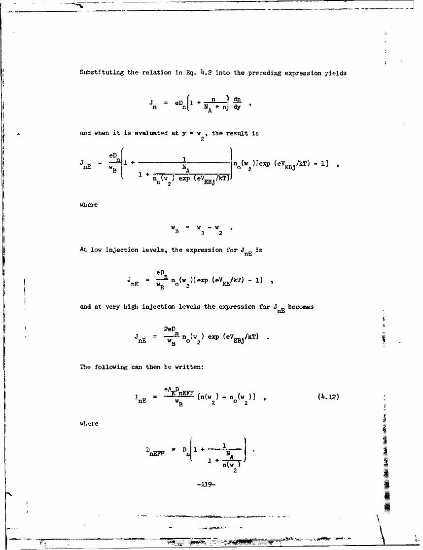
Substituting the relation in Eq. 4.2 into the preceding expression yields
-- eD 1+A ,n N A + nld '
and when it is evaluated at y = w , the result is2
eD ________(w I )[exp (eV±T) 1_
E+ A noT"2
0 2 () exp (eV /kT)J
where
B 3 2
At low injection levels, the expression for JnE is
eDJ = -- n (w)[exp (eV /kT) -1]
wB 0 2
and at very high injection levels the expression for JnE becomes
nn
2eDJ If n(w 2exp (eV f kT)
The following can then be written:
T eAEDnEFF [n( - n (v (4.12)-hE wB 2 0 2
where
D D I +- ]nEFF nA
n(w)2
-1.19
I
=~==-.- _ ____ ____

Depletion region widths w , w and w can be calculated by1 2 3
using the following analytical expressions:
~~ 11/2 _ _ _ _ _
1 t(,2 + '4 1 A (4.13)
= 1/2
BI EBJ
and
CE(Vw )
- WB eN 0 (4.15)
where V is calculated by using Eq. 4.4 and E(w ) is provided byEBJ B
0the collector simulation computer program CCP which is discussed in
Section 1.2.3. The Early effect 3 of base width modulation is included
in this device model through Eqs. 4.14 and 4.15.
An expression for the emitter particle current, which is valid
at any injection level, can be obtained from Eq. 3.] by replacing
Dn, n(w 2), p(- w ), VEB, and wB with the appropriate expressions that1 0
have been derived in this section. The emitter particle current is
given by
A [n(v) - (1 + - w) - po(- l (4.16)E t 2 1 o 2 WE 1
where
-120-
7__

II
WE W w if w - w < L0~0 0 P
and
WE -L if w, - v > L
The charge on each side of the emitter-base junction is
EL = e., = ew2"
Using the preceding relations yields
IT =3 d(VBI - V . ,i )
f/ 2- (lI2)=f2e t--H + d-14 - (hFEy)
The displacement current through CTE is i and is given byCTm
dV EBJ dt
dY= TE dt
dVTE dt "
The emitter-base diffusion capacitance CD is associated with the storage
of Lnority carriers in the bulk base region. If straight-line minority
carrier distribution and n(w ) = 0 are assumed, the total minority3
carrier charge stored in the neutral base region is
-121-I
.\ I

1-- = e EwBno(w) exp (eVIJ/kT)
and the current associated with CDE is
dB'CDE - dt
d% dVSBJ
dV dtEBJ
dVE- ChE d - " (4.19)
where
CD -dVEBj
- B (4s.2o)kT nE 2DnEFF
In reality n(w ) cannot be zero6 3 because nonzero electron current3
density exists at y = w . Because of nonzero n(v ), an additional3 3
charge will be stored in the base. Kirk5 1 showed that the fluctuation
of this stored charge in response to the input signal will introduce an
additional time delay, approximately equal to 1B/Vns , where v is theas
electron saturated velocity. There is another time delay which is
associated with emitter heavy doping. Until recently6C- 6 6 it had been
assmed that the emitter should be as heavily doped as possible in
order to ensure a high emitter injection efficiency. However, high
doping will lead to the formation of band-edge tails and impurity level
v- - F -

broadening64 '6 7 into an impurity band. DeMan64 introduced a
doping-dependent intrinsic carrier concentration ni to account for the
effect of heavy doping on the classical expressions for the electrical
parameters. The validity of this approach was later verified
theoretically.6 5'6 7 Under heavy doping conditions the hole current
density injected into the emitter from the base is given by6 8
J etn2 -
p P 2dy NI dy d
The holes experience an additional drift force proportional to the
derivative of the change of the valence band edge. Therefore an
additional component of hole current flowing from the base into the
eritter of an n-type CA&I' device is introduced . Aiditional holes
stored in the emitter cause an emitter delay time given by
4.1 I i (w -nffY ~Dylye eJ 0 0 Ni j D t%2 I
00 p i
where o 0 (D nN v w D p w ). herefore, microwave CAT? devices are0 0
designed to have narrow emitter Junction depths not only to reduce
the emitter capacitance and the emitter sidewall capacitance, but also
to reduce T e Henderson and Scarbrough69 considered the special case
of flat arsenic and boron concentrations in the emitter region. In
this case N and n. are both constant and therefore T is given by
E aT 0
e sB2 '
12D-.p 0
-123-
Nw

By including the two additional time delays, an effective diffusion
capacitance can be defined as follows:
wB 0
CO..? tTInfaJ~) + +w .(s.l
_DF .I nE ..CDE kT FF is 2D B2(.
Er n p 01
The base spreading resistance is calculated by using Eq. 3.19
and for conxenience it is stated again below:
B = +2 oBL BBJ number of emitter-base finger pairs1 2
where the device structure is defined in Fig. 3.2. Base region
conductivity modulation due to electron and hole carriers and the base
region width modulation due to the Early effect are ignored in Eq. 3.19
alt-houngh these effects can easily be included in the analysis.
The computer program for the emitter-base region EBCP solves the
circuit model in Fig. 4.3. It is assumed that Vsigt e B and I the
total collector current, are known quatities where the current I is
provided by the collector computer program COP. Kirchhoff's voltage
law demands
sa (t) dtVSig~t - VEB(t) - IIE('VEB) + [CTEZ("EB) + CDE(VEB)] d
- Ic(t)J o .
This equation can be written as
1 [V. (t) - VER(]dt V + V i t. Sig
+ It I,(VEB) (4.22)
-AP-- _
__\
~?r~ ~ -

1E
VD
I l
FI.1.3EUVL7CR~I ~ITE
GUTEAi EN
v-125
RU~ ~ - ---- ,------ --Raa
C- - -VE -+

which is the differential equation to be solved numerically by the
computer program EBIP. This differential equation is a first-order
ordinary differential equation of the form
= g(t,f)dt
and can be solved by +the fourth-order Runge-Kutta method:
t + f(t)+ (k+ + k) , (4.23)
2 3 4
where k = g[tVt)],1
k = gt + (At/2), f(t) + k (At/2)].2 1
k = gt + (At/2), f(t) + k (At/a)] and3 2
k gft + At, f(t) + k 3At!.
The assumption that C(t) is a known quantity, at this point, appearsartificial because i is knwn to be dependent on the electron particle
c
current injected into the collector region which is dependent on 'VE-.
and V is the =mknown quantity being naserically evaluated. This
apparent dilem is resolved in Section 4.2.4.
4.2.3 Collector ?sio LR-_Sij l Model and the Collector
Si-ulation Subroutine C P.
4.2.3a Equations to be Solved and the Simulation Technique.
The collector sisalation subroutine CCP consists of two parts: a
large-signal simulation subprograa £Z5! and a collector circuit com~ter
subprogram CCC. The iteration scheme is illustrated in Fig. 4.4. ten
CCP is called into operation, V, J. Vb~s andC are kaovn
quantities where
I
jC bins zw cn
-126-
VAT

VT (t) I +
(a)
I T
T +
(b)
I-
ii
i2-
FI.oi# TECOLCORIE ATINSHM. ())
-12TT
c.-- - C
c ci
__(-b)-- - Ic-- A- D V T -r ARE CACUAED IT -B T,

and
J = base transport factor x J = sech W- J (4.25)nBnEL nEn
The collector depletion capacitance1 2 is given by
C = Ci + R + R CbJ (number of emitter-base finger pairs) ,
(4.26)
where
dRL,
2 x, dB£
2
w
PbbI 12xBL ajj
C. =I "T
and
C = 2£ dt
b d% WT
The definitions of the device geometrical parameters are included in
Fig. 3.2. The computer subprogram LSSP is used to calculate JT, with
VT and JnB as known quantities. The computer subprogram CCCP is used
to calculate VT, JCc and J with VCB' JT' Cc and ZL as given quantities.
Figure 4.5 shows the block diagram of collector simulation subroutine
CCP. The assumption that VCB and JnB are known quantities appears
-128-
N

:ICA rX
CA LWGI -
em f* .
FIG.4.5 LOC DIARAMOF' ARGESIGAL SBROTINECC?
1T T729
to

artificial because V and J are J dependent and Jc is the quantityCB nB cC
being numerically calculated. This dilemma is resolved in Section 4.2.4.
4.2.3b Subprogram LSSP. The subroutine program LSSP is
based on a device simulation program developed at the Electron Physics
Laboratory written from the point of view of computational efficiency
by Bauhahn and Hadded. 6 2 The subprogram LSSP obtains a spatially one-
dimensional solution of the continuity equations, Poisson's equation, and
the current expressions obtained from a first-order solution of the
Boltzmann transport equation. Figure 4.6 presents the basic flow of
the simulation. If the electric field, carrier concentrations, VT and
J are known at a particular time t, Fig. 4.6 illustrates how theT
electric field, carrier concentrations, VT and JT at t + At are obtained.
Note that currents are defined to be positive in the direction of the
electric field. The simulation is voltage driven, therefore VT(t + At)T
must be given. As shown in Fig. 4.6, the first step is to solve the
continuity equations and obtain p(t + At) and n(t + At) where G is the
generation rate (C-s- -cm- 3 ) and x is the one-dimensional spatial
coordinate (cm). Carrier concentrations at t + At can be obtained
because the derivatives of p and n with respect to time in the finite-
difference approximations include p(t + At) and n(t + At) terms. The
second step is using Poisson's equation to obtain E(t + At) to within
a constant of integration. This constant is determined by requiring that
the integral of the electric field across the collector region equals
the base-collector voltage VT at t + At. At this point, the carrier
concentrations and the electric2 field at t + At are known. In Step 3
the carrier velocities at t + At are determined since the electric field
at t + At is known where v are the saturated hole and electronps ,ns
-130-

e G[E(xt)] . (A)at ax
a n (xt)-L( G[E(xt nB)
yields p(t + At) , n(t + At)
2. e E(t + At) e[p(x,t + at) - n(xt + At) - N?(x)]
subject to: VT(t + &t) T TE(t + At) dx
yields E(t + At)+
3. v (t + At~x) v Vp ,1- exp [-E(x.t + 4t)lUp /Vpsn]
yields v p,n(t + At,x)
1. J (x,t + At) = ep(x,t + At)v (x,t + At) - eD ap(t + At)p p ax
Jn(xt + At) = en(x,t + At)vn(x,t + At) + eD 3n(t + At)n t+t)nn ax
T "TO r0
yields J (x,t + At)pin
5. G[E(X~t + At)] Ap ex [-b /E(x,t +At)JJ (x,t + 601
+ An exp [-b /E(xt + At)]IJ (xt + At)j
FIG. 4.6 EQUATIONS SOLVED AND SEQUENCE OF STEPS.
I -131-

velocities (cm-s-1 ) and v are the hole and electron low-field
mobilities (cm-V-1-s-), respectively. Step 4 shows the expressions
used to calculate the current densities at t + At where J are thep,n
hole and electron current densities and J is the collector terminalT
particle current density which is found by integrating the particle
current densities throughout the collector region. It should be pointed
out that J is not the total collector current density because it doesT
not include the displacement current, which must be supplied externally.
The total current density at any point x is a constant and can be written
as follows:
= Jp(X) + Jn(X) + (4.27)
Integrating from x = 0 to x = wT yields
S wT [Jp(x) + Jn(X)] dx+. -WTE(x)dx
0 0
avT +-s (14.28)T + at
Step 5 is used to determine the generation rate G: whose expression is
given in Step 5 of Fig. 4.6. The values of a and ai are determinedn p
experimentally and can be calculated by using Tables 2.1 and 2.2. After
these five steps of calculation, everything about the collector region
at t + At is known. A new driving voltage value at t + 2At is specified
and the cycle is repeated.
4.2.3c The Difference Equations in Computer Subpro Lam LSSP.
The difference eq ,-s used to solve the differential equations of
-132-
N
\~

Fig. 4.6 are presented here. Figure 4.7 shows the space-time grid used
for the differential equations where the index K refers to the time step,
the index J refers to the carrier space step, and the index I refers
to the field space step.
The continuity equations are approximated by
- (p- (j)K G-1AtL/e - - Ax (429)
and
(n)+l - .K
.) (= K + Jn-i (.3o)At/e A (x 3
were At is the time step; Ax is the space step; and the generation rate,
assuming that only pure avalanche generation occurs in the collector
region, is given by
I 1 IGK + 1 (G ) _ "(4.31)
(j )K KK
= a)~IJ~ +(a)Ir ~ (4.32)
The time step At is limited in this case by the dielectric relaxation
timeb2 which is given by
< CAt = +p (4.33)-- e(nun p
where pn and p are the electron and hole mobilities. Poisson's equation
becomes
-133-
N______________________________________

P+ I I n+1-"I L AXI2
I iI II I
I I 2 23 240 0 0 0 ---
2 24 25
(0) CARRIER CONCENTRATIONS
(0) ELECTRIC FIELD. PARTICLE CURRENTS. GENERATION RATES
(a)
(J+l, K+I)(I+I, K+I) (J, K+I) (I, K+I) (J+l, K+I}
xle [At
(J-I, K) (-1, K) (J, K) (I, K) (J+l, K)
(b)
FIG. .7 SPACE-TIME MESH USED TO WRITE THE DIFFERENCE EQUATIONS.
(a) SPACE MEH. (b) SPACE-TIME MESH.
S- --- 1-=-
K K K(E)K- (E)K 1 (p)-(n)j + (ND) J
Ax /de
where E is the electric field and N is the donor doping density in theD
collector region. The transport equations for electrons and holes
become
K+I K+l(j fL= ~p) p - K( ) j (p)iK K~( )K ()'
and
K+I K+1K(n) (n)
=e(n)J K (v) K + e- (.36
for (E)K > 0 and
-~l_ , K+I
KKK.KK ()K1 Ki= e(pl-( (14.37)(J +1 pI p I A
and
(nK (n)K+IK K KK
e(n) (v)I e(D )I s 3nIi nnI Ax(13)
for (E) K 0, where v and v are given by the expressions
(K v ep E1(439)*p PS vP
and
(v )K = exp ( 4.40)
respectively, and D and D are the field-dependent electron and hole
n p
-135-

diffusion coefficients. The drift terms in the current density
equations use "upwind" carriers and are explicit. The reason for
the name upwind can be seen in Eqs. 4.35 through 4.38, i.e., in
order to calculate the particle current at (I,K), the particle
concentration in the direction opposing the particle flow, in the
upwind direction, is used. The diffusion terms are implicit. This
completes the semiconductor difference equations.
The voltage constraint stated in Step 2 of Fig. 4.6,
VT(t + At) = f T dx, (1.4)
0
can be expressed as follows:
NSTEP(V K = xNTP(4.42)
1=1
where Ns'nA w,/Ax and the field index i = 1,2,... ,NSTEP.
The electron current density at the base-collector metallrgical
Jiuction is assumed to be equal to the electron current density at the
edge of the base-collector depletion region since the width of the
base-collector depletion region into the base region is very small.
Host of the carrier generation occurs in the depleted collector region.
The electric field at the base-collector metallurgical Junction is
always above the electric field necessary to sustain electron and hole
carrier saturation velocities. If the electron end hole carrier
densities at the base-collector meta~lurgical junction are defined to
be
-136-
N|

JnBt)
n fV
ns
and
Jp(tI-I-D
P B t ) =
Us
respectively, where v and v are the electron and hole carrierns
sat-ration velocities and the avalanche multiplication piroduced hole
current .1 - is calculated by the subprogram 123P, the actual current
den ties at this boundary will be significantly lower than J andnfl
The reason for this is that there are large magnitude electron
and ole diffusion currents flowing in the opposite direction to the
drift current components. Figure k.8 contains the schematic distribution
profiles of electron and hole densities in the depleted collector
region. A set of "current conserving" boundary conditions will now be
der ved. When the electric field is pointing in the direction opposing
that of the space coordinate x, as in n-type CATT devices, the following
is- obtained:
p ep p,
an d
a = env -eD in n n it
wIc- can be written as
- (P)K - (P1()K -- e(D (v)K + eD +
Pl 1 P I P I A
-137-

COLLECTOR REGION-
P+ n n n
p
-Jw
b(b
z0
o ELECTRON DENSITY
u HOLE DENSITY
DISTANCE, x
(C)
FIG. 4.8 (a) COLLECTOR REGION, (b) jE(x)l PROFILE AND
(c) ELECTRON AND HOLE 0ONCENTRATION PROFILES.
-138-
=I
and
K ,KVK 2(J)r" = e(n) (V - e(D) 2
n n
The boundary conditions are obtained from these equations by rearranging
the terms and they are
J (Bt) + eD (n)K/Ax
(t)3i n 2*an ').n1 lA (4-js3)
PB(t) ev - eD Ax
s n
and() A ) t(J )K ad the0 IL
where B3 (t) =(n)K ,p, oRK nl() P n h
indexes I and 2 represent the space point at the metallurgical Junction
and the space point next to the Junction, respectively. The carrier
velocities are assumed to be at the saturation values and the diffusion
constants have the low field values.
.2.3d Subprogrm CCC . The circuit problem to be solved
by CCC? is shown in Fig. 4.. The differential equations to be solved
are
dt
and

=~d f1 __ d 2 % _____ dVICE __ dI,
dt +CC Tt dt Ct.dtc dt- .,c -
C~ C. C +C R.T C*C I ?'
anz they are of the form
df
dt 2 12
Tersolutioscnb bandb usi ng the foufl-h-order Runge-Kut-ta
LR 2 L -Iteation Scheme Wihich Couiples the E=ite-Base Region
and the Collcotor Rerion Simulaticms. PreYviously_ the .. -- is of MBCPand ZC ( aS ad CCC?) wer discuss-ed. Th1le 'trton snn no
couz' e'sE~ and CCP is described in Fig. 4.0 Wnicn i the block
~arem of the cernlete large-si =--zI eoaqputersi ltinpor.
mag-ga-. situlatioris usir ER-C? and C#P, (ietermine
twr 'er FZ, i3 1 1 amI vy Fr-n these
results th e CAWT asrpil fer out- RW paer, pow~ m r =-nd
u,,Acec can h- determined. _1 0a '=-m MaCn. -
nB' UT end Vmr=, the case Ixn wrs - +e load a ,de4-Q tank circ
rhose rosan- fre' .uency Is tmed2 - s'a 'm-ray Fgure JhI
NI

FA=
-4-
j~~ ft.. v Zts
141

2000 s0
-70
1500- T -60
nB.T50 >
vbia, sz 1000 -- -....... ... 40
0-30 >
500- 20
10u0
0 40 80 120 160 200 240 280 320 360
ANGLE, 9
(a I
loss fO'- 0.14* 0,2w
,o-- V -
K1144E -
10• :2F4
2 4o1- -*44
:2 9 0
0 1 2 3 4 0 1 2 3 4 0 1 -3 4 0 1 2 3 4
DISTANKE. pam
FIG. 4. O (a) JnB, JT AND VT WAVEFORMS AND (b) DISTRIBUTION
PLOTS OF ELECTRON DENSITY (MINUS SIGNS), HOLE DENSITY
(PLUS SIGNS), AND ELE CTR IC FIELD PROFILE (SOLID LINES).
(xxx RPEET THE REGION WHERE THE ELE CTR IC FIELD
HAS REVERSED ITS DIRECTION)
S-142-
-N
1 4* .

shows the distribution plots of electron and hole densities and the
electric field profile at var~ous phase angles. At 8 = 18 degrees
an insignificant number of electrons is injected into the collector
region, at e = 108 degrees a large number of electrons is injected and
they undergo avalanche multiplication, at e = 144 degrees electron
carriers drift across the depleted collector region, and at 8 = 288
degrees most of the electron carriers have been collected at the collector
contact.
4.4 Imr mnts Over Previous -Si Simulation of Class C
CATT Amplifiers
The computer large-signal simulation program described in this
chapter has eliminated the following inadequacies contained in the large-
signal simulation by Yu et al.:3 3
1. Emitter-base high-injection level effects were not incorporated.
2. Effects of high emitter doping level, minority carrier induced
electric field in the base region, and a nonzero minority carrier density
at the base-side edge of the base-collector depletion region were
ignored.
3. The Early effect was ignored.
4. Diffusion currents in the depleted collector region were
ignored.
5. A current nonconserving boundary condition for minority
carriers in the depleted collector region was employed.
6. in determining the feedback hole current in an n-type CATT
device, a time-averaged carrier multiplication factor was used which
_143-
I%a

is valid only if the emitter-base injected charge is very narrow and
the carriers generated due to the base-collector reverse saturation
current are negligible.
4.5 Conclusions
In this chapter, analytical expressions for the circuit model of
the emitter-base region were derived. These expressions are valid at
any injection level. The Early effect, high emitter doping density
effect, and nonzero n(v ) effect were taken into consideration. The3
collector region is modeled by employing a differ.nce-equations version
of the semiconductor differential equations. Descriptions were given
for the numerical methods used. Field dependences of charge carrier
drift velocities, diffusion constants and ionization coefficients,
and the space-charge effect were included in modeling the collector
region. The iteration scheme which couples the emitter-base circuit
model and the collector region is described. The iteration scheme
is constructed in such a way that the time step size for EBCP, LSSP and
CCCP can be independently different from each other. This feature is
very convenient and can save much unnecessary simulation cost.
_144-_

CHAPTER V. LARGE-SIGNAL STUDIES FOR CLASS C CATT AMPLIFIERS
AND COM ARISON WITH CLASS C BJT AMPLIFIERS
5.1 Introduction
In this chapter large-signal results of Class C CATT and BJT
amplifiers are obtained from the computer simulation model developed
in the previous chapter. This study is concerned with a series of
X-band CATT devices with uniformly doped and HI-LO collector structures
and a series of X-band BJTs with uniformly doped collecto~r structures.
The main distinction between the CA?"' devices and the BJTs is that the
avalanche multiplication factor of the latter is always limited to
1.1 or less. The effects of impurity doping levels and widths of the
base and the collector regions and the optimum dc bias and load are
investigated at various input power levels and operating frequencies.
The Class C CATT and BJT amplifiers are compared on the basis of their
efficiency, power gain, and the device inherent bandwidth.
5.2 Lare-Signal Simulation Results for Class C CATT Amplifiers
5.2.1 General Discussion. The following study shows the
effects of avalanche multiplication and wide collector regions. Large-
signal simulations of Class C CATT amplifiers with various impurity
doping levels and widths of the base and collector regions are carried
out. The usefulness and the limitation of carrier multiplication and
long collector transit angles are explored. The optimum values of the
device parameters are determined. The amplifier inherent bandwidth,
dynamic range, power gain, efficiency, optimum dc bias and optimum
load are investigated.
-IN -145-
The following large-signal simulations used the label DEV:material,
type, letter, N( (cm 3 ), WT (Um) for devices with uniformly dopedC
collectors and DEV:material, type, letter, N (cm-), w (Um),av av
Ndrif t (cm-3 ), wD (jim) for devices with HI-LO collector regions, where
the symbols Nc, wT, N , w, NI and w have been defined previously.c V v drift D
Therefore, DEV:Si,n,A,2 x 1016,1.1,1 x 1015,2.9 is the label used for
a Si device which has an emitter-base structure A and a collector
structure whose avalanche multiplication region is impurity doped
at 2 x 1016 cm- and is 1.1 Um wide, and whose drift region is impurity
doped at 1 x 10" cm - and is 2.9 Uim wide. The geometrical dimensions
and the impurity doping levels of the emitter-base structures simulated
are listed in Table 5..
5.2.2 Qptimum Load. The optimum load for a Class C CATT amplifier
is the same as thar for a Class C BJT amplifier. To obtain maximum
RF power at the fundamental harmonic, the load should be a high Q,
parallel RLC tank circuit which, in combination with the collector cold
capacitance Cc, has a resonant frequency equal to that of the emitter-
base driving signal. With such a load, a typical set of J T(t), V T(t)
and the emitter-base injected charge carrier waveforms is shown in
Fig. 5.1 where the effective dynamic multiplication factor M is definedA
as:,T
MA J0 JT(t) dt (5.1)J[JnB(t) +Jc c d0 ns ps
and q is the overall amplifier efficiency. The aforeentiored optimum
load condition can be derived as follows. The average output power is
-146-
= - %
- ____ -

0
4iU tc
4-,0m C U -
-. 4 ii 1 t
ca~0
43,C
co UN
4,
09
0
4, 14*
43 :
-147 SR

4xIO3 --. o8
vT 70
3 -60
-50'
-2T -4
30o
I2-0i \ -20
0 40 60 120 160200240280320 300, DUG/EES
.x 3"l! so ,
-V T -60
-50'
2- T -40
-30
, I 20
00 40 80 120 16200240 280320360
U. OEGRES
(b)
FIG. 5.1 (a) JT AND VT WAVEFORMS WHEN R IS OPTIM
(G = 9.74 dB, n a55 PERCENT, VRF, = 3 .3 V
AND MA = 1.o36). (b) JT AND VT WAVEFORM WHEN
% IS GREATER THA THE OPTIM VALE (G
9.15 dB, n = 52 PERCENT, VRF = 33 V. MA
1.053). (DEV:Si.n,B,6 x 101S,2; f = 1245 GHz;
V Sg(t) = 1.1 sin wt - 0.191 V; Vbias = 40 V)
-1148-

II
g givn by
Pout = T Ic(t)VT(t) dt (5.2)
0
where T is the RF period. Since I (t) + t) Cf(dv/dt),,c T ±
"out IT(t)V(t) dt (53)0 T
if iT(t) and VT(t) are expressed in terms of their harmonic components,TI
to. 3 becomes
out = ITd VT + lITC VT cos 8 + lIT IIVT I cos 2 + '1
dco 0 2 2 n
li I cos +... (5.4)n
where 8 is the phase difference between the nth harmonic components ofn
l4t) and VJt). Under optimum load conditions, current component
t sees a nearly pure resistive load and all higher harmonics of IT(t)-TT
see nearly a zero impedance. Therefore, 8 is approximately Tr rad and1
V 0 Vfor n 2.n
The resistor P1 of the parallel RLC load should be such that an
optimum VT(t) is produced. For a given dc bias, if P, is below the
optimum value, a small amplitude VT is produced which means less output
power. If R. is too large, an overly large V will be mpressed across
thv collector region which will cause a decrease in both the amplifier
efficiency and the available power to the load. This may be due to two
different reasons or to a combination of the two depending on the do
bias. First, an extremely large-amplitude RF voltage causes the electric
field in significant portions of the drift region to be depressed below
j -b9-
-!£-o- -
. - -- - ~ =4fl

that necessary to sustain carriers at a saturated velocity during a
significant portion of their transit across the drift region. Two
consequences follow which reduce the efficiency and the output power.
The JT(t) and VTCt) waveforms corresponding to this situation are
shown in Fig. 5.1. The slowing down of charge carriers caused the large
depression in the Jm(t) waveform vhich is highly detrimental to the±
efficiency and power output since the depression occurs near the
minimum of V(t). The slowing down of the charge carriers also causedT
an expansion in the vidth of the J(t) wav-eform which means lowera
efficiency. The reduction in efficiency i4 more severe at higher
collector transit angles due to the functional dependence of efficiency
on sin (0J2)/(e,2) There 0_ = /V If - ra" , an expansion
in the width of the JT(t) waveform could mean that large conduction
current would be flowing during the positive hal:-'cyle of the nearly
sinusoidal V (t) which meats energy dissipation. Second, having aT
large-amplitude RF voltage impressed across the collector causes the
electric field in the avalanche multiplication region to bec
extremely high when VT(t) is maximum so that a significant pulse of
charge, produced bry the avalanche multiplication of the thermally
generated collector reverse saturation current, is injected into the
drift region. This pulse of charge is injected much earlier than the
emitter-base injected pulse of charge. Thus, the effective width
of the JT(t) wave1-.m is significantly increased and therfore the
efficiency is reduced drastically. The J, and VT waveforms corresponding
to the second case are shown in Fig. 5.2.
5.2.3 Dc Bias. It was mentioned previously that a high-efficiency,
high-gain CATT amplifier requires a dc bias such that both a
-150-
F>__

4X0380
VT 70
60
S-50
oz 2 '40
20
-0
0
so
I -20/ \ 0,
0 4060,20 O ZO024O3zoMO0
*. O)EG;EES
4.)
4x - 0
70
b T -VT5 4
-302 h0
'1 30
o 40 80 120 M02002402 0 3 2 0 3 0
. DOEREES(0)
FIG. 5.2 () T ADt VTwAvm, vM; H IS OpTDO
(G = 1 0 75 d, n 1 43 PEREN~o V = 27.2 V
AND MA 1.107). (b) T N VT Wv IMW
RLIS WTnj TA THEz op'rnM VALUE (G - 3T dB*p]- -" .9 PERCEN, VRF - 28 v AN = 1.6T).
A; (DEV:Si.,.B6 x iOls.2; f = 2.75 Gli; V g(t) =
-S5g
large-amplitude V T(t) and a significant multiplication factor occur.
The effects of the dc bias on the amplifier performance can be illustrated
by the results given in Table 5.2. Figure 5.3 shows the optimum JT and
V, waveforms of a typical h-urm CAM device at different dc biases. TheA
operating frequency is 12.75 GHz. The optimum dc bias is 65 V. At a
lower dc bias, i.e., 60 V, both the allowed amplitude of VT(t) and the
multiplication factor are reduced. The output power, power gain and
efficiency are also decreased. At a de bias higher than the timum
value, i.e., 80 V, although the multiplication factor is higher, the
allowed amplitude of V (t) decreases drastically which leads to lower
output power, lower power gain and lower efficiency. The drastic
reduction of the amplitude of V_ is due to the fact that when the dc
bias is significantly higher than the optimum value, a large-amplitude
T(t) would cause an injection of a charge pulse at a phase angle much
earlier than the emitter-base injected signal charge. This prematurely
injected pulse of charge is the result of avalanche multiplication of
the thermally generated collector reverse saturation current under an
extremely high electri- fi &2. The effective width of JT(t) widens,
therefore, efficiency decreases. The device also loses its controlled
avalanche characteristics.
When the emitter-base driving signal is varied in its amplitude,
the amoumt of charge carriers injected into the collector region variesas well, it was found that as the amplitude of the driving signal
increases the optimum dc bias for optimum gain and efficiency decreases
sli fly. This is due to the space-charge effect of the injected
charge carriers from the emitter-base junction. A larger number of
injected carriers results in lower carrier multiplication, and the
-1N

I
Table 5.2
Effects of Dc Bias on Amplifier Performance
1EV'Tjizn,A,2.2xOI6,1-1,2xlO ,-.; V 1.15 sin ult -. 2 V;f !.75 GiS
btias R. Voltage Amnlitude M. out-y_) (v) A (iL ) (Percent
5.j 12 b.25 7.5lO 3 10
5 17 5.65 8.UO33 16.5
52.5 2h 5.5 8.5flO3 25
C 28.5 5.5 8.5xO 3 28
22. 5 •.25co 3 22.5
DE:Si'nB,6xlO1 ,h; Ysg = 1.1 sin wt - 0.191 V; f 12.75 Zfz
zlas iF Voltage oult G p.VIL mlitul MV " W=tt 2) (Per-ent) " ii'
so "2.5 2.3 2.kx0 4 13 U.n
73 r. 1 1.83 2.9 8xIo0 25 11.413
65 42.4- 1.75 2.9 6 x10⁴ 38.1 .24
&3 38.7 1.71 2. 63x1O 3h.1 Th.58
55 u1.8 1.43 2.09xl? 32.9 13.22
35 12.9 19 8.197X0 3 21.4 8.05
(Cont.)
-151-_I
- - -)

ale 5.2 (Cont.)
D~q . " ,,B~xll6,; usig =1.1 sin t 0 .1-1 V;, f =12.75 GHz
-. VotWIas R Vol age out n p(V) A- 1itude- (v) "A (w/&:- ) (Percent) (dB)
5..4 3.1 2.985x10⁴ 20.7 12.99
52.5 26.h 2.76 3.47lxJ4 26.8 I4.55
50 31 2.69 3.384 xi1& 25.1 i4!.8
47.5 27.8 2..1 .72 22.6 13.73
45 2.t 2.iz 2.08x1i 20 12.z3
10 15.5 1.53 1.23x290 17.1 9.65
-15.4-
_ I ~- S ~ -=-~---- -

sms 120
S0 3 -1T004 60 -0 \ -o
-70 sO
0 /- \ -6it 37 -6O -704: 3- 60
2- -40/
-30 2 40
20 30
4 60 120 60 200 240260320 340 0
e) 0 40 S0 2i0So mm, &judo 330360
lbS
6xlOI o110
5 : 100
4 i-o
'I0 4- -o- f'I J0
L •12 1 I 1_I I k 10
0 40 60 120 160 200 2402803 0 3o
AMC. 8(c)
FIG. 5.3 JT AND VT OF A TYPICAL 4 x 10⁻⁴ cm COLLECTOR
DEVICE OPERATING AT 12.75 GHz AND MAXIMUM ALLOWED
RF VOLTAGE AMPLITUDE. (a) DC BIAS BELOW THE
OPTIMUM VALUE, (b) DC BIAS ABOVE THE OPTIMUM VALUE,
AND (c) AT OPTIMUM, DC BIAS. (DEV:SI,n,B,6 x 1015,4)
-155-

importance of carrier multiplication in determining the amplifier
gain and output power of a given CATT device at the optimum operating
condition relative to that of the RF voltage amplitude is reduced.
The variation in optimum de bias as a function of tie emitter-base
driving signal level is illustrated in Table 5.3. The space-charge
effect is illustrated in Figs. 5.4 and 5.5. Plots of electrle field
profile, electron and hole eistributions at various phase angles, and
J and V waveforms corresponding to two different emitter-baseT T
signal levels are shown. The device is DEV:Si,n,B,6 x i015,4.
The profiles of the electric field at various phase angles explain
the reduction of MA as the driving signal level is increased. It isIA
also observed that V , the 'inimum allowed VT, is lower due to space
charge and therefore the maximum allowed RF voltage amplitude increases
slightly with increa-sing Vsig , assuming V is kept constant.Sig bias
The optimum dc bias also varies with the operating frequency.
It was found that, for a given device, the optimum dc bias increases
with increasing operating frequency. This is because as the operating
frequency increases the transit angle increases; therefore, charge
carriers are injected into £he depleted collector earlier in a given
cycle when the value of V T (t) is higher. Avalanche multiplication
becomes a more important factor in determining the gain and the RF
output power. Avalanche multip-ication is a sensitive function of the
electric field. The variazion of optimum dc bias with operating
frequency is illustrated by the results tabulated in Table 5.4.
5.2.4 Effects of N ay Ndrift and wD in HI-LO Collector
Structures. The effects of varying Nay, w a, Ndrif t and wD are
examined in this section. The results given in Table 5.5 give the
-156-
l - --- - . - . .

Table 5.3
Variation Of Optimumr Dc Bias with Emitter-Base Signal Level
DEV:Si,n,B4I x 1016,h; f 12.75 Gflz
(V) Optimum Dc RF Vo.Ltage
g JBias (V) Amplitude (v) !A
1.05 sin :t - 0.1823 55 26.3 3.98
1.10 sin wt - 0.191 51.5 29 2.71
1.15 sin wt - 0.199 51 31 1.75
1.20 sIn wt - 0.2083 48.5 34 1.57
1.25 sin wt - 0.217 46 38.1 1.45
DEV:Si,n,B,6 x 1015,h; f= 12.75 GHz
1.05 sin wt - 0.1823 70 ho 2.55
1.10 sin wt - 0.191 65 42.h 1.75
1.15 sin ws - 0.199 64 49.6 1.57
1.2 sin wt - 0.2084 63.5 50 1.37
f
I{
I
ei
4
-L5°• AM
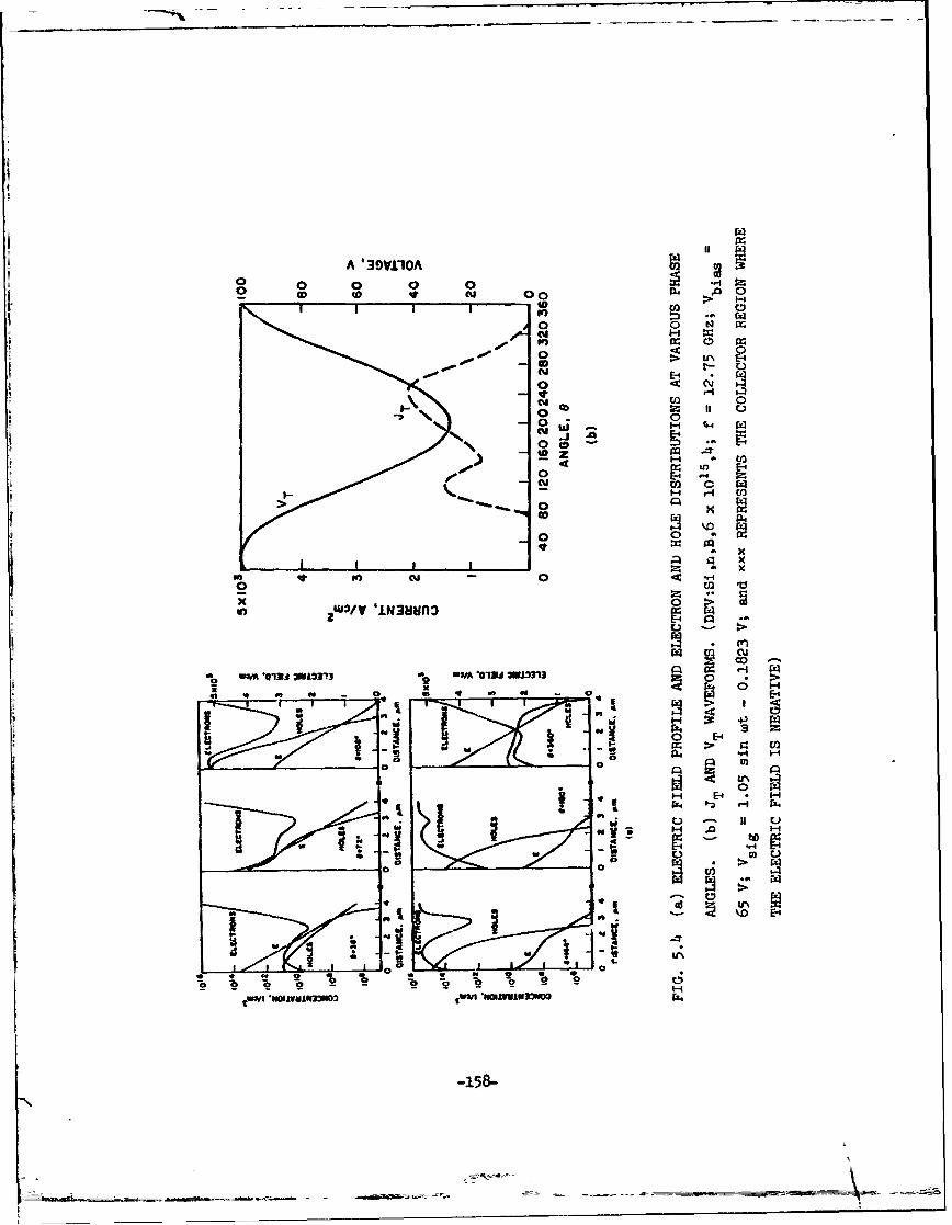
A '39VL1OA0 OD o N 0 0Io .
CDfo C4
0 ~ < N
0)CWC.)
z- Cl)
aot
00
0~14 'i3&ti
lo 3- c z
0 n
x 0a2V'N~u:
b b b 1,
-158-.
-~~~~~w
mom-.----.---- P4--(.
~ ----
______

A '39YJ10A 94
0 0 0 00 V 00
, 0 A 0
-~0 N- 0z
p.0 0l
0 Ea 4 0
0
4' x
0 m
W0 x 1
z r
0 0
'-4
IL a.
4b ±5 P
_ _ _ _ _ __ _ _ ___on$
- ~ ___ ND

Table 5.4
Variation or Optimum Dc Bias with Operating Frequency
(DEV:Si,n,B,2.2 x 1016,1.1,2 x 1015,2.9)
Optimum Dc
f (GHz) Bias (V)-
7 50
10 52.5
12-75 52.5
14 55
18 57
21 57.5
V. 1.05 sin wt-0.1823 VSiLg
7 50
12.75 52.5
21 57.5
V. 1.0 sinc wt Q.1736 VSig
7 50
12.75 52.5
21 55
-160-
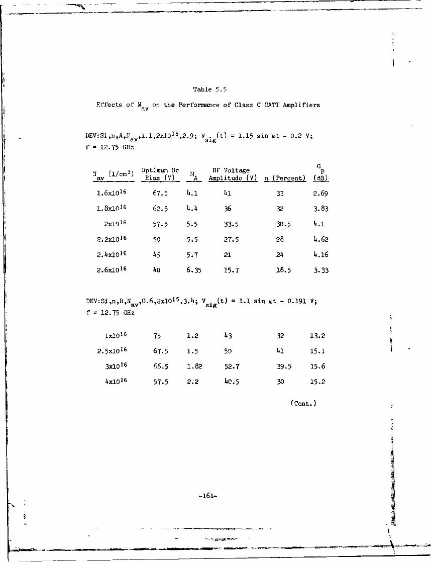
Table 5.5
Effects of N on the Performance of Class C CATT Amplifiersav
DEV:Si,n,A,N av. ,2xlOIS,2.9; V sig(t) = 1.15 sin wt - 0.2 V;
f = 12.75 GHz
GN (1/cm3 ) Optlmum Dc RF Voltage pav Bias (V) _A Amplitude (V) n (Percent) (dB)
1.6xlO 16 67.5 4.1 41 33 2.69
.8y-10 16 62.5 4.4 36 32 3.83
2x10 16 57.5 5.5 33.5 30.5 4.1
2.2x10 16 50 5.5 27.5 28 4.62
2.14xi01 6 45 5.7 21 24 4.16
2.6x10 16 4o 6.35 15.7 18.5 3.33
DEV:Si,n,B,N ,o.6 ,2x1015,3.4 ; Vs.g(t) 1.1 sin wt - 0.191 V;av 3.;vSig
- 12.75 GHz
Ex10 16 75 1.2 43 32 13.2
2.5xlO1 6 67.5 1.5 50 41 15.1
3x10 16 66.5 1.82 52.7 39.5 15.6
4X1O16 57.5 2.2 40.5 30 15.2
(Cont.)
-161-
AM

Table 5.5 (Cont.)
DEV:Si,n,B,N ,.8,2xl1OS,3.2- V (t) 1.1 sin wt - 0.191 V;av 'Sig
f = 12.75 GHz
Na (/cm 3) Optimum Dc RF Voltage G
av ' Bias (V) MA Amplitude (v) r (Percent) (dB)
ix1016 75 1.3 45.5 33 13.9
1.75x10⁶ 70 1.6 50 38.5 15.2
2xlO16 65 1.7 46.5 39 15.1
2.25x10¹⁶ 63.5 1.8 44.2 38 15.4
2.5xlO IE 62 2 42 34.5 15.4
3.5xlO 16 47.5 2.42 25 27.5 12.7
DEV:Si,n,B,N av,1.2,2x101 5,2.8" VSigt) = 1.1 sin wt - 0.191 V;
1 = 12.75 GHz
5xlO 15 80 1.35 46.5 31.5 13.8
ix10 16 72.5 1.5 49.2 37.5 14.8
1.5x70 16 63.5 1.95 41 34.5 15.3
1.75x]0 16 60 2.15 35 28.5 15
2,10 16 53.5 2.4 30.5 26 13.8
-162-
-~ ------ - -~=t~~ - - - - __%

optimum performances of CATT devices with different N and wav av
For a fixed w there is a corresponding optimum N . For devicesav av
with Na higher than the optimum value, larger avalanche multiplicationav
is achieved at the device optimum dc bias, but the amplitude of V T is
decreased. The resultant efficiency, output power and power gain are
lowered. If N is lower than the optimum value, although the amplitudeav
of VT may be slightly higher, the avalanche multiplication is lower.
For devices with wider avalanche multiplication regions, the optimum
a would be lower in order to maintain the device capability for largeav
amplitude V As long as the avalanche multiplication region is not
too narrow or too wide, i.e., 0.6 to 1.2 lim, there is no significant
difference in the performance of devices with optimized Nav
The effects of drift region width and its doping level have
also been examined. Large-signal simulations have been carried out for
devices with emitter-base structure A. The operating f'-quency is kept
at 12.75 GHz. The results are summarized in Table 5.6. The results
indicate that the longer devices have higher optimum dc biases, higher
multiplication and lower efficiencies. Higher multiplic. on is due to
a longer collector transit angle which implies an. earlier injection
of carriers in a given cycle when the value of V T(t) is higher. Lower
efficiency is due to its dependence on sin (e.T/2)/(e9,2). The amplitudeA A
of VT, output power and po;er gain increase with increasing wD until
w,, Ls approximately 5.5 Pm. At f = 12.75 GHz, the w, which corresponds
to a r-rad collector transit angle is 4 um. It was indicated previously
that a collector transit angle greater than v rad implies a large current
flow during portions of the positive half-cycle of V(t) and, therefore,
a large amount of ener#y dissipated. However, due to larger carrier
-163-

Table 5.6
Effects of Drift Region Width
DE:Si,n,A,2.2xl0 1 6 ,1.i,2x0] 5 ,WD; V ( t) = 1.15 sin wt - 0.2;D sIigf 12.75 GHz
1,m) Optimum Dc RF Voltage pWD Bias (V) n (Percent) 'A Amplitude (V) dB)
2.1 45 30 3.7 22.5 2.36
2.4 47.5 29.5 34.3 24.6 3.03
2.? 50 28 5.2 26 3.55
2.9 52.5 27.5 5.9 27 4.36
3.15 52.5 27 6.4 29 5.2
3.4 55 26.5 7.3 30.5 6.h1
3.65 57.5 24.c, 8.5 32.5 7.52
3.9 6o 21.5 9.6 33 8.61
4.4 65 15 11.3 33.2 9.0a4
4.65 67.5 13.5 11 30 7.81
5.15 70 8.25 10 29 6.03
-164-
___________________\
_________________________________________

multiplication and RF voltage ampli-tude, the optimum w_ for maximumI
output power and pnoer gain is 5. i. As w., is increased beyond
5.5 pm, efficiency becomes verY low and the maximum allowed RF voltage
am~i-tude sta- to decrease. The decrease in HF voltage am.m--'d ....... dcras. .1 apitude i
cue to the increae in w'tn increasing wT while the breakdown
electric field intensity stays co.ntant. If efficiency and power
gain are both considered, the optmu w_ at 12.75 3Hz is J .5 to
t .75 urm.
The dr-f m-ron doping density should Le as low as vossible
S4inlmlze , :.e., m-.aimize thealled RFS voltee. But itSUS
should be suffi ciet to sutain the charge carrier derity. Otherwise,
he soace-charge effect will force the electric field behind the
charge pulse in the drift region to be depressed below the charge
carrier saturation drift velocity sustaining value. As a consequence.
charge carriers at the tail end of the pulse will be sloed down and
the-. charge pulse will spread out which, in turn, will cause a decrease
zn the fundamental ha-rmonic component of I. This is one aspect of
te deterioration in amplifier pow-er gain and efficiency due to space
charge in a igtly doped drift region. Depression of electric field
behind the charrepuse, when severe enough, will brinr a reduction in
te' allowed maxium RF voltage amplitude. it can be seen from large-
stial simu.lat'on results that at a low input signal level the device
with the sm-allest NA has the largest allowed RF voltsge amplitude.
As the input signal level increases the allowed manIm m voltage
amoitude of the device with the smallest N.ift decreases noticeably.
i i- is the other aspect or the detfrioration in amplifier p;er gain,-i' -165-
I

power output and efficiency due to space charge in the lightly doped
drift region.
Table 5.7 summarizes the results of large-signal simulations of
devices with various values of N f. The electric field depression,
charge pulse spreading and reduction in VRF due to space charge are
illustrated in Figs. 5.6 through 5.9. It is also observed that space
charge in a lightly doped drift region may force up the electric field
intensity near the collector contact and a significant number of
electron-hole pairs will be created. This will further expand the
duration of the induced current, increase power dissipation and reduce
the efficiency.
5.2.5 Uniformly Doped Collector Structures. Large-signal
simulations of devices with uniformly doped collectors have been
carried out. The results are summarized in Table 5.8. These results
correspond to the operating condition when both the power gain and the
efficiency are optimized. The following observations can be made:
. Shorter devices have higher efficiencies. The higher efficiency
is due to a higher V JV-. ratio and a smaller collector transitHr bias
angle. At f = 12.75 GHz, however, efficiency reaches a saturation
value when the collector region width is reduced to 2 &m and it will
not increase significantly if w, is further reduced.
2. Longer devices have higher output power and power gain. The
higher output power is due to a larger allowed HF voltage amplitude and
a higher avalanche multiplication factor. The higher multiplication
factor is due to a higher optiwm dc bias and an earlier injection of
charge carriers into the collector region relative to the VT waveform.
-166-
I
-- |

Table 5.7
Effects of N dr ft
DEV:Si,n,B,2.2xlO1 6 ,1.1,'41015,2.9; f = 12.75 GHz; V = 45 Vbias
RF Voltage G
sig VA Amplitude () n (Percent) (dB)
sin wt- 0.1736 6.4. 23.3 23.5 15.7
1.05 sin wt - 0.1823 3.5 24.3 27.5 14.9
1.I S wnl - 0.191 2.35 24.7 26 13.7
1.15 sin - 0.2 1.98 24.3 20.2 12.4
1.2 sin at - 0.2084 1.68 22 16 10.5
JL :Si,n ,l,2.23l6,l.l3110 5.2.9; f 12.75 GHz; bias = 7.
sin t - 0.1736 5.5 25 26 15.5
1.05 sin wt - 0.1823 3.-4 27.5 27 14.9
1.1 sin t - 0.191 2.45 28 24.5 13.9
1.15 sin A 0.2 1.96 27 18. 38 12.2
".2 sin 0 0.2084 . 27.5 13. 10.5
coant.)
-161-

Table 5. fCont.)
DEIV:Sin,3-2XO16 . .l,2x101 5 ,.9; f 2.5 GjHz; V.. = 52.5 VC 83
RF Voltage psIg (V)A- Atiitude (V)n (Percent) (dB)
0.9 Sin wt -0.165 6.7. 12.
Unt - 0.1736 4.4 2.5 28 1.65
-in -t - -.1-2 3 _5 28 ik.8
1 In W*0.191 ca. 1 4. 30.2
sn wt -0. 1.96 29.7 17 12.3
0.284 L.71 27.1 13.3 lO.4
:S,,,.. ,... ,-2xi 1. V = 12.75 CAz; Va = 58.5 V
sin wt - 0.1736 4.37 33.8 30 _0
1.05 -I- t - 0.1 2 302. 15.6
1.I--in wt- 0.191 2.35 3135 19.7 13.72
1.15 -n wt -0.2 1.79 2.5 i.6
1.2 sin wt o.2 3"3 l1.6 0.6
-168-
" ii -

Not".0 r
x 0
U~~~A~~I~~ua HU2h b lg~~1
00
_0 -0I
0 0
= 0 0 0 0
-i fo S1
1 4b0 00
R -aq
0 InH
/
4%4
U- N
L~ 6

U)
N -
U,
x
n to
*0 4 - 0 0 0 4 5
4 41U
0' I to
Es- t)-' p
E4 CL
0 0 2
-4 - 0 in w -) 0
N
-170-

rI
A to
*6 0
p.
A *39YflOA
o 0 00o0000 -
0
*ft~ft
00
eft 0
7.3*c

Co E-4
W 0
'-4o1
9: .41-
WN -~~9~t CIL.-~
0 E-100c
- -M4
16 -a pt
0~~ ~ ~ 0 ~F in
0~
0 * P
4-0 w >.4-
.0- 0
4
4 % 4 . . 3

Table 5.8Large-Signal Simulation Results of CAiT Devices with
Uniformly Doped Collector Structures
DEV:Si,n,B,N ,5; f = 12.75 GHz; V . (t) 1.1 sin wt - 0.191 V
I. (ilm 3 ) Optimum Do HF Voltage p- Bias (V) "A Apli tude (V) P, (Percent) (dB)2x1o15 80 1.12 38 22 11.86b10I1 73.5 3.63 57.7 29.9 i8.61
I 6 5-.. 2.6 27.5 23.2 14.55
1.25xL016 45 2.69 24.9 19 13.3
DEV:Si,n,B , 4; f - 12.75 GHz; Vg(t ) = 1.1 sin wt - 0.191 V
2x10¹⁵ 70 1.05 41.5 38 12.8
4XlO15 70 1.42 45.5 38 13.9
tXIo 15 63.5 1.72 41.5 38.5 15.8
8.- xl o15 56.5 2.55 36.5 29.5 16.7ix1016 51.5 2. 29.5 26.5 1.86
I%27:Si,n.,B,N ; f = 12. 7 0Hz; V t = 1.1 sin wt - 0.191 VSig
2x-0 15 4 5 1.05 36.5 %.5 n.6
6xi 15 56.5 1.35 36 14 12.31x1O16 47.5 2.11 33 32 U.S
(Cont.) _
r-173-N_ _ _ _

Table 5.8 (cont.)
DEV:Si,n,B,N c2; f =12.75 Ghz;, V Si (t) =1.1 sin wt -0.191 V
N(1/iM) Optimum De H F Voltage G________ Bias(v) n (Percei.1) (dB)
2x10¹⁵ 33 1.0 28.5 55 10
&05 3T.5 1.02 29 52 10.2
JXIO16 14o 1.o6 214.4 14T 10.2

3. The optimum N0 is approximately 6 x 10 5 c W- t ith a higher
Nc, the avalanche multiplication factor may be higher at the optimum
do bias, but the permissible V is consistently lover. The differencehRF
in the allowed VRF is pronounced when wT = 3.5 um and f - 12.75 GHz.
To maintain a large permissible VF, due to an increase in V with-F sUs
increasing VT, the optimum dc bias of devices with N. 1 x 10¹⁶ cM- 3
TC
actually decreases with increasing wT if wT > 4 on. The consequences
can be a decreased 4 and a decreased permissible VRF. Devices with
.< 6 x l0 I cm 3 at their optimum dc bias suffer from a smaller
avalanche multiplication Tactor and space charge is more likely to
reduce the prmissible VF. The space-charge effects were discussed inHF
Sections 5.2.3 and 5.2.4.
I. Performance of dez'ice DEV:Si,n,B,6 x 1015,4 compares very
favorably with that of devices with various 4 um HI-ID collector
structures at f = 12.T5 GHz and V Sig (t) - 1.1 sin ut - 0.191 V. The
results are summarized in Tables .55 and 5.6. A CATT device with a
uniformly doped collector can be fabricated more easily. The
dynamic rage and inherent bandwidths of devices with HI-LO and
uniformly doped collectors are compared and discussed in a later section.
5. It has been shown that VRF shouli be as large as possible to
maximize tte power gain and efficiency. When VHF equals the maximm
permissible value, there is a considerable amount of charge carriers
generated from avalanche multiplication of the charge carriers of the
collector reverse saturation current during the time period when VT
is near its maximum value. This is also true for devices with HI-LO
collector structures. Therefore, a more exact definition of MA is
-175-
i 'S

jT JT(t) dt
MA T JIT[JnB( t ) + Je + Jc ] t
ns ps
0
This expression implies that the induced collector terminal current
JT(t) is due to avalanche multiplication of both the charge carriers of
the emitter-base injected current and the collector reverse saturation
current, although the former is usually the dominant one.
.3 & -Signal Simulation Results for Class C BJT Amplifiers
The operation of Class C BJT amplifiers can be considered as a
special mode of operation ofthe previously simulated three-terminal
devices operated as Class C CATT amplifiers. The difference lies in
the combination of collector transit angle, base-collector de bias and
amplitude of VRF which results in a collector multiplication factor of
1.1 or less for BJT amplifiers.
Since avalanche multiplication does not play an important role
in determining the performance of Class C BJT amplifiers, only devices
with uniformly doped collectors have been simulated. The results of
large-signal simulations of various Class C BT amplifiers operating at
12.75 GQz are suarized in Table 5.9. The following observations can
be made:
1. For devices with any WT, those with the lowest N consistently0
have the best performance as long as space-charge density in the
collector region is not excessively high. This is due to the restriction
on MA which makes VRF the only major factor in determining amplifier
performance. Higher N implies higher Vsu s and V. Higher Vsu s and
VPT implies higher electric field in the vicinity of the base-collector
-176-
- - --
- - "-- ---- -, ~ -~---

Table 5.9
Large-Signal Simulation Results of Class C BJT Amplifiers
DEV:Si,n,Bj,5; f = 12.75 GHz; Vsig(t) - 1.1 sin wt - 0.191 V
He ( I/ r3o ) Optimum Dc RF Voltage pG
-- -- - Bias (V) MA Amplitude (V) n (Percent)
2xloI5 70 i.06 32.9 20 10.89
6x10¹⁵ 36.5 1.1 13 14.5 7.31z10 1 6 always operates as a CATT amplifier when V - VpT
X1 awasbias P
DEV:Si,n,B,N1,4; f = 12.75 GHz; VSig (t) - 1.1 sin Wt - 0.191 V
2xlO15 70 1.05 41.5 39 12.8
4x I s 55 1.1 21 40.5 12.55
6x10I5 35 1.1 12.8 21.7 8.o6
8.5X10¹⁵ 32.5 1.1 10.5 13.5 6.53
ixiOI6 always operates as a CATT amplifier when V - V
DW.':Si,n,B,N ,3; f 12.715 0Hz; V i(t) = 1.1 sin Wt - 0.191 V
2xO 15 1.5 1.05 36.5 56.5 1i.6
6xo' 5 50 1.1 33.5 47 12
X1o16 27.5 1.1 14.4 20 7.5
(cont.)
NI
I S

Table 5.9 (Cont.)
DEV:Si,n4B,N ,2; f - 12.75 GHz; V -C(t) = 1.1 sin wt - 0.191 V
N (iicm3 ) Optimum DC RF Voltage pc Bias (V) M A Amplitude (I) n (Percent) (dB)
2xloI 33 1.0 28.5 55 10
6xlo35 37.5 1.02 29 52 10.2
IXlO16 4o 1.06 24.4 h7 10.2
I
I
-178-
1

junction. When MA is restricted to 1.1 or less, therefore, devices
with higher N have a lower maximum allowed VF. This points out onec E
major difference in the design of CATT and BJT amplifiers.
2. aximm power gain is achieved by the device
DEV:Si,n,B,2 x 1015,4 while for CATT devices maximum power gain is
achieved by devices with collectors 5 im or longer. As for BTT
amplifiers, longer devices have a large collector transit angle which
implies that charge carriers injected from the emitter-base junction
reach the multiplication region when V is higher. Since H isT A
restricted to 1.1 or less, therefore, a longer device has a smaler
maximm permissible VRF when vT = 3 un. If the collector is intrinsic
or extremely lightly doped, maxima power gain would be achieved by a
longer device, but the maxim current density vould be limited by the
afurementioned space-charge effects ad therefore the device output
power will be limited. The reductions in maxima permissible Vip and
power gain with increasing v, are very pronounced in devices with
N = 6 x l091 ei3 and VT = 3.5 zm. This points out another differencecT
in the design of CATT and BJT amplifiers.
3. Devices with vT = 2.5 pa, when operating at optimu conditions,
are EXT amplifiers independent of the waLues of Ne . The performance
of the device with Nc = 1 x 1016 cm- 3 is a ost the same as that of
the device with Nc 2 x 10¹⁵ c - 3 at Vig(t) 1 l.l sin wt -0.191 V.
At T = 2 um, higher Nc may be desirable due to increased current
capability of the device.
14. A shorter device has a higher efficiency.
Comparisons between the Class C CATT and BJT amplifiers are
carried out in the next section.
-179-

5.4 Coeparison Between the Class C CATT Amplifier and the Class C BJT
Anaplifier
5.4.1 RF Power Gain and Efficienc- at f -12.75 GHz and
V .(t) = 1.1 sin wt - 0.191 V. Large-Signal simulatIons of devicesSig
with VT ranging from 2 UM to 5 pm and U from 2 x i01' cz - 3 to
I x 1016 cu- 3 , operating at 12.75 GHz and V ig (t) - 1.1 sin wt - 0.191 V
were carried out and the results are sumarized in Tables 5.8 and 5.9.
it is observed that a maximum G of 18.61 dB at 29.9 percent efficiencyp
is achieved by DEV:Si,n,B,6 x 1015,5 operating as a CATT amplifier as
compared to a maximum G of 12.8 dB at .39-percent efficiency achiendP
by DEV:SinB,2 x 1015, 4 operating as a BT amplifier. An additional
5.8-dB power gain at the expense of 10-ptrcent efficiency reductior
cm be developed by employing a suitable CATT amplifier. if
D EV:Si,n.,6 x 1015,4 operating as a CATT amplifier is used, a 15.8-dB
power gain at 38.5-percent efficiency can be achieved. Thus a well-
designed CATT amplifier can achieve the same efficiency and a 3-4B
additional power gain as compared to the maxima gain BJT amplifier at
12.75 G:z. The higher gain is mainly due to a multiplication factor
of 1.72 and, to a lesser extent, a slightly larger allowed V.. If
DEV:Siu B.6 x 1015,3 Ua is operating as a CATT amplifier, a power gain
of 12.3 4B can be achieved vhich is approximately the mciar power gain
achievable by the BJT amplifier at 12.75 Wiz. However, due to its
shorter collector region, CATT amplifier DEV:Si ,,,6 x 10S,3 has a
higher efficiency than the maimn gain BJT alifier.
It was noted previously that devices with vT 'C 2.5 i, when
operating at optimm conditions and f = 12.75 GCz, are BJT alifiers
since their mltiplication factors are less than 1.1. The BJT amliflers
-180-
N

with wT = 2.5 um have higher efficiencies but lower power gain than the
CAT1T amplifiers.
5.h.2 Dynamic Range. The dynamic ranges of various CATT
amplifiers and BJT amplifiers were investigated and the results are
discussed in this section. The Vbias is kept constant at the optimum
V corresponding to V (t) = 1.1 sin t - 0.191 V, although itbias Sig
was shown previously that the optimum V varies slightly with thebias
input signal level.
From Fig. 5.10 it is observed that G and r of both the CATT andp
BJT amplifiers are low at low input signal levels. This is due to
low emitter indection efficiency at low input signal levels at an
operating frequency of 12.75 GHz. At high input signal levels, GP
and n of both the CATT and BJT amplifiers deteriorate. In the case of
CATT amplifiers, the deteriorations in G and n are due to space-charge-P
caused reductions in M and V and space-charge-caused spreading inA HF
the induced current waveform. High injection level effects in the
emitter-base region is another cause. In the case of BJT amplifiers,
all the aforementioned are causes for reductions in G and n at higherP
input signal levels except the reduction in 1 A. By definition, MA is
never greater than 1.1 for BJT amplifiers.
By comparing Figs. 5.10a and b, it is seen that
DEV:Si,n,B,l x 1016,4 has comparable G at low input signal levels,p
i.e., P. S 1 x lO- W, as does DEV:Si,n,B,6 x 1015,4. Its C reducesIn P
faster with increasing P. in the range 1 x 10 - W < P. 5in in
than that of DEV:Si,n,B,6 x 1015,4 due to the fact that M Is a moreA
important factor in determining its G and MA L. very sensitive to any
space-charge-caused reduction in the electric field during emitter-base
-181-
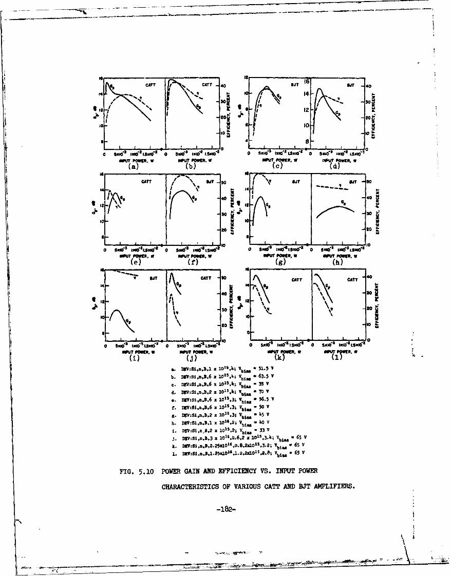
=CA"? CAT 40 car WT0
(4 10- 0 14-
10 8 10 V
14 -3' -4, * 5 -
I I: 4 -30
I V
o0g sgo 0 xsIete w xtv i
molPOE. uou OW.w O POWR . wJ NowER w
CAT? 40
12- 't. If _ _ __ _ _ _ __ _ _ _
0~~ -to 3-OISIZ 0 310 l)I ~I 4 0 510(i) 30 7
ER ka. ?;S1n.3, i 0~'.~ 5.5
b0 16.iu56z~ M.-6.C. Dv:8,nJ, z 0~.; T
bt~a35
d.Z2:1J20 W -to& ~ 7.VA 4H:1i.. O',;~ M*5.
h.mv:S,ia.b1 x lo1Bl; v~ bim 55v
c. D3V:S1n.3.,2 1015.4; V 1 s , 33 Vdj. DEV:1n.S.2 x 105.; v bi ,3Jr ab, 70 v
k. MEY:E1,n,2.2Z11
,.3;8.1 5
3. a ~ 45 65
1. DIY:S,n,.1.25ZO'.1.2.2I10' 5.2.8; vu, 0 65 V
FIG. 5.10 POWER GAIN AND EFFICIENCY VS. INPUT POWER
CHARACTERISTICS OF VARIOUS CA IT AND BJT AMPLIFIERS.
-182-

charge injection. For P. > 5 x 10- 3 W, the rate of reduction in Gin p
is slower for DEV:Si,n,B,l x 1016,4 because MA is no longer as important
in determining G and the space-charge effect in the low-field driftP
region of DEV:Si,n,B,l x 1016,4 is not as severe as in
DEV:Si,n,B,6 x 1015,4. This explains the even faster rate of reduction
in G of DEV:Si,n,B,2 x 1015,4 as shown in Fig. 5.10d. Of the threep
devices with uniformly doped collectors, DEV:Si,nB,6 x 1015,4 has the
best G and n characteristics. All three devices with HI-LO collectorp
structures, whose G and n characteristics are shown in Figs. 5.10JP
through 1, are very inferior to DEV:Si,n,B,6 x 1015,4.
Devices ihose G and n characteristics are shown in Figs. 5.10c, fP
and g through, i are BJT amplifiers. It is observed that the amplifier
dynamic range is severely reduced when N is too low (due to space-chargec
effects) and shorter devices with properly designed N have lower powerc
gains but higher efficiencies and a wider dynamic range. The wide
dynamic range associated with a short device, i.e., wT = 2 um, is due
to the fact that MA .1 at optimum V even at low input signal
levels and therefore an almost constant MA, independent of space charge,A-
exists. •
5.4.3 Inherent Bandwidth. Plots of G , V and M vs.
frequency for CATT and BJT amplifiers are shown in Figs. 5.11 through
5.13. The decrease in G for a short BJT amplifier, i.e.,p
DEV:Si,n,B,6 x 1015,2, can be attributed to well-known causes such as
the emitter-base RC frequency cutoff mechanism, base and collector
time delay, and collector capacitor charging time. Since M is limited
to 1.1 or less for the BJT, V decreases slightly as frequency isP'F
increased. This is shown in Fig. 5.13. This decrease in V also playsRF
-183-
__ _ N
____ ____ ____ ____= -_=:A

16 60
15- 650 w
14 -40
w
0 4w 2 1 0 2
04
503 30
0 4 s 12 16 20 24FREQUENCY, GHz
(b)
FIG 5.. LS4 ATAPIIE EFR C S RQ C
AI50. V)F
Vbia
MA T
30 -

60
14 z
40.
0 30
11 2
0 4 8 12 16 20 24FREOLENCY, G~z
60 4
50 -VRF -3
~40-
30- -- 1
20 00 4 8 12 16 20 24
FREOUENCY. GIz
(b)
FIG. 5.12 CLUS C BJT ANPLFIER PERFOMANCE VS. FR~EQUENCY
AT CONISTANT INPUTl POWER LEME. (DEV:Si,n,B,2 x 11.
ANDY7 uTO)Vbias
-185-

14 80
13 -70
1-2 60,:0(3
z
Id1
Io I(3 I 4
10 1400 4 8 12 16 20 24
FREQUENCY, GHz
(a)
40 4
30 3
S20 -2
MA"A"
10 .. .. . . -1
I I I I iI o-
0 4 8 12 16 20 24
FREQUENCY. GHz
(b)
FIG. 5.13 CLASS C BJT APLIMFIM PERFORMICE VS. FREUCY
AT CONSTANT INPUT POWER LEVEL. (DEV:Si,n,B,6 x 1015,2
AND vbi" -3T.5 V)biaB

I
a role in the decrease of G and ,. For a longer BJT amplifier, i.e.,p
DEV:Si,n,B,2 x 10154,, the decrease in VRF is more severe in order to
keep MA 1.1. Thus, G and n decrease more rapidly with frequency
as shown in Fig. 5.12. The inherent bandwidth of the 2-im BJT is wider
than the 4-pm BJT. For a CAfl amplifier, MA is allowed to take on anyIAvalue as long as it is not too high and a stable operation cannot be
achieved. The RF voltage amplitude VHF of CATT device
DEV:Si,n,B,6 x 1015, stays constant up to 1 GHz. For higher
frequencies, V., decreases with increasing frequency in order to
maintain stable operation. This decrease in VRF results in decreases
in G and n. As frequency increases, M also increases which helps top A
offset the decrease in G . This explains the slower rate of decreasep
in 0 as compared to that of r. The Is-ur CAT7 amplifier has a muchp
wider inherent bandwidth than the 4-u BT amplifier.
5 ConclusionsLarge-signal simulation results for both the Class C CAT ? and
Class C BC amplifier were presented in this chapter. The optimum de
bias condition, optimum load and their variations iith frequency were
investigated. Me effects of device structural parameters were
studied and opti=mm device structures for both the CATT and the BJT
amplifier operating at 12.75 GHz were obtained. Several differences
in the design of optimum CATT and RiT amplifiers were derived from
the large-signal simulation results. Comparison between the CATT
and the KIT amplifiers in terms of gain, efficiency, dynamic range and
inteinsic bandwidth were also given.
-8
i r
CHAPTER VI. SUMMARY, CONCLUSIONS, AND SUGGESTIONS
FOR FURTHER STUDY
6.1 Summary and Conclusions
The purpose of this study was to investigate the effects of
avalanche multiplication and transit time in the collector region of a
BJT. Analytical equations, circuit models, and computer simulations
were used to determine dc, small-signal, and large-signal behavior of
CATT amplifiers.
In Chapter 'I a dc computer program was developed which determines
the dc avalanche multiplication factor vs. V characteristics forVbias
any Si or GaAs collector structure. The results provide an estimation
of device large-signal performance capability. The optimum collector
parameters, i.e., V , N , N obtained from the dc computer program
correspond well to the results of large-signal simulation. Results
also indicate that an n-type Si CATT amplifier is superior to p-type
Si and n-type GaAs CATT amplifiers due to its favorable MA vs. Vbis0
characteristics.
In Chapter IllI analytical models of de and small-signal charac-
teristics for CATT devices with Read-type collector structures were
given which incorporated both the avalanche multiplication and the
collector transit-time mechanisms. Contrary to previous findings, the
small-signal characteristics of Class A CATT amplifiers indicated that
a larger avalanche multiplication factor results in a smaller RF power
gain and an increase in MA does not necessarily imply a significant0
increase in f Ma" Results were given and discussed. One conclusion
was the inapplicability of CATT devices as Class A amplifiers.
-!88..

In Chapter IV a large-signal computer simulation was developed
which incorporated several improvements over the large-signal simulation
previously reported,33 i.e., high injection level effects in the base
region, Farly effect, effect of high impurity level in the emitter,
nonzero minority carrier concentration at the edge of the base-collector
depletion region on the base side, minority carrier induced electric
field in the base region, current conserving boundary condition for
minority carriers in the collector region, and diffusion current in
the collector depletion region.
In Chapter V large-signal results of Class C CATT amplifiers
were given. Effects of base-collector dc bias, load, operating frequency
and collector structures were examined and discussed. The simulation
calculates output power, power gain, and efficiency of the amplifier.
It also gives emitter-base current and voltage waveforms; avalanche
multiplication factor; JT and V waveforms; and spatial distributionsT T
of electrons, holes, and electric field in the collector depletion region
at any time instant. Various Si n-type CATT and BJT Class C amplifiers
operating at 12.75 GHz were compared in terms of output power, power =
gain, efficiency, and dynamic range. Optimum collector impurity doping
level and optimum width of the collector region of both the CATT and BJT
amplifiers were determined and discussed. Carrier multiplication and
long collector transit time do increase power gain, but at the expense
of lower efficiency and smaller dynamic range. Avalanche multiplication
does help to increase the device inherent bandwidth.
6.2 Suggestions for Further Stuy
In the course of this study several additional topics which need
further exploration were found. They are as follows:
-189-

1. A cost-tolerable, two-dimensional, large-signal computer
simulation program to account for the nonuniform injection of carriers
at the emitter-base junction and the nonuniform injection of carriers
into the collector region due to nonuniform emitter-base junction
potential across the emitter finger laterally caused by the flow c"-
conventional base current and feedback hole current in a resistive base
region.
2. Fabrication of X-band CATT devices and experimental studies
of Class C CATT amplifiers.
3. Construction of new models for use at higher frequencies.
4. Small-signal and large-signal noise theories for CATT devices.
5. Thermal limitation studies.
6. Application of CATT devices as high-voltage, high-current
drivers.
-190-

LIST OF REFERENCES
1. Bardeen, J. and Brattain, W. H., "The Transistor, A SemiconductorTriode," Phys. e., vol. 7h, No. 2, pp. 230-231, 15 July 1948.
2. Shockley, W., "The Theory of p-n JL- ctions in Semiconductors and
p-n Junction Transistors," Bell System Tech. J., vol. 28, No. 3,pp. 435-489, July 1949.
3. Early, J. M, "Effect of Space Charge Layer Widening in JunctionTransistors," Proc. IRE, vol. h0, No. U. pp. 1401-1406, November1952.
4. Pritchard, F. L., "Frequency Variations of Junction-TransistorParameters," Proc. IRE, vol. 42, No. 5, pp. 786-799, May 1954.
5. Sbers, J. J. and Mol, J. L., "Large-Signal Behavior of JunctionTransistors," Prc IRE, vol. 42, No. 12, pp. 1761-1772, December1954.
6. filetcher, N. H., "Some Aspects or the Design of Power Transistors,"Proc. IRE, vol. 43, go. 5. pp. 551-559, May 1955.
7. Ereis, R., Herlett. A. and Spenke, E., "The Effective Emitter Areaof Power Transistors," Pro c. IRE, vol. 46, No. 6, pp. 1220-1229.June 1958.
8. Johnson, E. 5., "Physical Limitations on Frequency and P erParameters of Transistors," RCA Rev., vol. 26, No. 2, pp. 163-1TT, June 1965.
9. Whitter, R. J. and Tremere, D. A., "Current Gain and Cut-OffFrequency Fall-Cff at High Currents," TEEE Tran-. on ElectronDevices, vol. ED-16, No. 1, pp. 39-57, January 1)69.
10. Bailey, R. L., "large-Signal Nonlinear Analysis of a High-PowerHigh-frequency Junction Transistor," IEEE Trans. on ElectronDevices, vol. ED-17, No. 2, pp. 108-119, February 1970.
11. Cooke, H. F., "Microwave Transistors: Theory and Design," Proc.IEEE, vol. 59, No. 8, pp. 1163-1181, August 1971.
12. uite, .. H. and Thurston, M. 0., "Characterization of MicrowaveTransistors," Solid-State Electronics, vol. 13, No. 5, pp. 523-542,Hay 1970.
13. Kurokava, K., "Power Waves and the Scattering Matrix," IEEE Trans.on Microwave~ s and Techiques, vol. fl11-13, No. 3, 1w2O2, .March 195-
[791 -

14. Wahl, A. J., "Distributed Theory for Microwave Bipolar Transistors,"IEEE Trans. on Electron Devices, vol. ED-21, No. 1, pp. 0-49,January 197h.
15. Shackle, P. W., "An Experimental Study of Distributed Effects in aMicrowave Bipolar Transistor," IEEE Trans. on Electron Devices,vol. ED-21, No. 1, pp. 32-39, January 1974.
16. Hall, R. N. and Dunlap, W. C., "p-n junctions Prepared by ImpurityDiffusion," nrs. Rev., vol. 80, No. 3, pp. 467-468, 1 November 1950.
17. Teal, G. K., Sparks, M. and Bmehlor, E., "Growth of GermaniuaSingle Crystals Containing p-n Junctions," fzs. Rev., vol. 81,No. 4, p. 637, 15 February 1951.
18. Pfann, W. H., "Principles of Zone-Refining," Trans. AIME, vol. 194,p. 747, 1952.
19. Tanenbaum, M. and Thomas, D. E., "Diffused Emitter and BaseSilicon Transistor," Bell System h. ., vol. 35, No. 1, pp. 1-22, January 1956.
20. Lee, C. A., "A High Frequency Diffused Base Germaniua Transistor,"Bell System Tech. J., vol. 35, No. 1, pp. 23-34, January 1956.
21. Theuerer, H. C., Kleimack, J. J., Loar, H. H. and Christenson, H.,"Epitaxial Diffused Transistors," fro. IRE, vol. 48, No. 9,pp. 1642-1643, September 1960.
22. Hoernl, J. A., "Planar Silicon Trnsistor and Diodes," Presentedat the International Electron Devices Meeting, Washington, DC,October 1960.
23. Lepselter, M. P., "Beam-Lead Technology," Bell e Tech. J.,vol. 45, No. 2, pp. 233-253, February 1966.
24. Shockley, W., u. S. Patent No. 2,787,564, 1954.
25. Gibbons, J. F., "Ion Implantation in Semiconductors-Part I, RangeDistribution Theory and Experiments," Proc. IEEE, vol. 56, No. 3,pp. 295-319, March 1968.
26. Yuan, H. T., Wu Y. S. and Kruger, J. B., "A 2-Watt X-Band SiliconPower Transistor," IEEE Tras. on Electron Devices, vol. ED-25,No. 6, pp. 731-736, June 1978.
27. Yu, S. P., Cady, W. R. and Tantraporn, W., "A New Three-TerminalMicrowave Power Amplifier," IEEE Trans. on Electron Devices, vol.ED-21, No. 1, p. 736, November 197.
28. Poou, H. C. and Meckwood, J. C.. "Modeling of Avalanche Effect inIntegral Charge Control Model," I "7ans. on Electron Devices,vol. ED-19, No. 1, pp. 90-97, January 1972.
-192-

I
29. Fossum, J. G., "A Bipolar Device Modeling Technique Applicable toComp ter-Aided Circuit Analysis and Design," IEEE Trans. on ElectronDevices, vol. ED-20, No. 6, pp. 582-593, June 1973.
30. Dutton, R. I., "Bipolar Transistor Modeling of Avalanche Generationfor Computer Circuit Simulation," IEEE Trans. on Electron Devices,vol. ED-22, No. 6, pp. 334-338, June 1975.
31. Rein, H. M., "Relationship Between Transient Response and OutputCharacteristics of Avalanche Transistors," Solid-State Electronics,vol. 20, No. 10, pp. 849-858, October 19T.
32. Yu, S. P., Cady, W. R., Eshbach, J. IL and Tantraporn, W., "Hot-HoleEffects and Experimental Results on the CATT at S-Band," IEEE ?- -.on Electron Devices, vol. ED-22, No. 1, p. 1066, November 1975.
33. Yu, S. P., Tantraporn, W. and Eshbach, J. R., "Theory of a NewThree-Terminal Microwave Power Amplifier," IEEE Trans. on ElectronDevices, vol. ED-23, No. 3, pp. 332-343, March 197-6.
34. Eshbach, J. R., Yu, S. P. and Cady, W. R., "Avalanche Multiplicationin CA"Ts," Solid-State and Electron Devices vol. 1, No. 1, pp. 9-16, September 1976.
35. Winstanley, A. M. and Carroll, J. E., "Transistor Improvement Usingan IMPATT Collector,' Electronics Letters vol. 10, No. 24, pp. 516-518, 28 November 1974.
36. Carroll, J. E., "The Third Terminal in Microwave Devices," Proc.fr!san Solid-State Device arch Conf., Nottingham, England,pp. 109-l32, Septmer 19714.
37. Quang, N. A., "Small-Signal Equivalent Circuit for IMPATTransistors," Electronics Letters. vol. .1, No. 21, pp. 503-504.16 October 1975.
38. Lefebvre, M., Crosnier, Y. and Salmer, G., "Amplification with3-Terminal Avalanche Devices," Electronics Letters, vol. 12, No. 7,pp. 154-155, 1 April 1976.
39. Anderson, L. K., McMullin, P. G., D'Asaro, L. A. and Goetzburg, A.,"Mic ve Photodiodes Exhibiting Microplasma-Free CarrierMultiplication," AwI. ra. Letters, vol. 6, No. 4, pp. 62-64,
15 February 1965.
40. Presser, A. and Belohoubek. E. F., "1-2 GHz High-Power LinearTransistor Amplifier," CA Rev., vol. 33, No. 4, pp. T37-751,December 1972.
41. Hartnn, K., Ktyczka, W. and Strutt, M.J.O., "Experimental GainParameters of Three Microwave-Bipolar Transistors in the 2-nto 8-GilRae," Proc. 1W, vol. 59, No. 12, pp. 1720-1721, Deceer 1971.
-193-
£ I
29. Fossum, J. G., "A Bipolar Device Modeling Technique Applicable toComputer-Aided Circuit Analysis and Design," IEEE Trans. on ElectronDevices, vol. ED-20, No. 6, pp. 582-593, June 1973.
30. Dutton, R. W., "Bipolar Transistor Modeling of Avalanche Generationfor Computer Circuit Simulation," IEEE Trans. on Electron Devices,vol. ED-22, No. 6. pp. 334-338, June 1915.
31. Rein, H. M., "Relationship Between Transient Response and OutputCharacteristics of Avalanche Transistors," Solid-State Electronics,vol. 20, No. 10, pp. 849-858, October 1977.
32. Yu, S. P., Cady* W. R., Eshbach, J. R and Tantraporn, W., "Hot-HoleEffects and Experimental Results on the CATT at S-Band," IEEE ?rzana.on Electron DevicesM, vol. ED-22, No. 1, p. 1066, November 1975.
33. Yu, S. P., Tantraporn, W. and Eshbach, J. R., "Theory of a NewThree-Terminal Microwave Power Amplifier," IEEE Trans. on ElectronDevices, vol. ED-23, No. 3, pp. 332-343, March 1976.
31. Eshbach, J. R., Yu, S. P. and Cady, W. R., "Avalanche Multiplicationin CATTs," Solid-State and Electron Devices, vol. 1, No. 1, pp. 9-16, September 197-
35. Winstanley, A. M. and Carroll, J. E., "Transistor Improvement Usingan IMXATT Collector," Electronics Letters, vol. 10, No. 21, pp. 516-518, 28 November 197.
36. Carroll, J. E., "The Third Terminal in Microwave Devices," Proc.EarPa Solid-State Device Research Cozf., Nottingham, England,pp. 109-132, September 1974.
37. Quang. N. A., "Small-Signal Equivalent Circuit for IMPATTTransistors," Electronics Letters vol. 11, No. 21, pp. 503-50,16 October 1975.
38. Lefebvre, M., Crosnier, Y. and Saluer, G., "Amplification with3-Terminal Avalanche Devices," Electronics Letters. vol. 12, No. 7,pp. 154-155, 1 April 1976.
39. Anderson, L. K., McMullin, P. G., D'Asaro, L. A. and Goetzburg, A.,"Microwave Photodiodes Efhibiting Microplasma-Free CarrierMultiplication," A pl. _frs. Letters, vol. 6, No. 4, pp. 62-6,15 February 1965.
ho. Presser, A. and Belohoubek, E. F., "1-2 Glz High-Power LinearTransistor Amplifier." RCA Rev., vol. 33, No. 1, pp. 737-751,December 1972.
41. Hartmann, K., Kotyczkas, V. and Strutt, M.J.O., "Experimental GainParameters of Three Micron-ve-Bipolar Transistors in the 2-'to 8-GHZRange," Proc. IEEE, vol. 59, No. 12, pp. 172- 11T-, December 1971.
-193-
V-Sur
55. Carson, R. S., High Freiuyency Amplifiers, Wiley-Interscience, NewYork, 1975.
56. Sanderson, A. C. and Jordan, A. G., "Electron Beam Control ofIMPATT Diodes," Solid-State Electronics, vol. 15, No. i, pp. l4O-h2, January 1972.
57. Forrest, J. R. and Seeds, A. J., "Optical Injection Locking ofIMPATT Oscillators," Electronics Letters, vol. 14, No. 19, pp. 626-627, 14 September 1978.
t 58. Schroeder, W. E. and Haddad, G. I., "Nonlinear Properties of IMPATTDevices" (Invited Paper), Proc. IEEE, vol. 61, No. 2, pp. 153-182,February 1973.
59. Lee, C. M., Lomax, R. J. and Haddad, G. I., "Semiconductor DeviceSimulation" (Invited Paper), IEEE Trans. on Microwave Theory andTechniques, vol. MTT-22, No. 3, PP. 160-177, March 1974.
60. Evans, W. J. and Haddad, G. I., "A Large-Signal Analysis of IMPATTDiodes," IEEE Trans. on Electron Devices, vol. ED-15, No. 10,pp. 708-717, October 1968.
61. Greiling, P. T. and Haddad, G. I., "Effect of Nonsaturated DriftVelocity on Avalanche-Diode Performance," Presented at the 1968International Electron Devices Meeting, Washington, DC, October1968.
62. Bauhahn, P. E. and Haddad, G. I., "IMPATT Device Simulation andProperties," IEEE Trans. on Electron Devices, vol. ED-24, No. 6,pp. 63h-642, June 1977.
63. Matz, A. W., "A Modification of the Theory of the Variation ofJunction Transistor Current Gain with Operating 1v!'nt andFrequency," J. Electronics and Control, vol. 7, No. 2, pp. 133-152, August 1959.
64. DeMan, H. J., "The Influence of 1heavy Doping on the EmitterEfficiency of a Bipolar Transistor," IEEE Trans. on ElectronDevices, vol. ED-18, No. 10, pp. 833-835, October 1971.
65. Mertens, F. P., DeMan, H. J. and van Overstraeten, R. J.,"Calculation of the Emitter Efficiency of Bipolar Transistors,"IEEE Trans. on Electron Devices, vol. ED-20, No. 9, pp. 772-778,September 1973.
66. Mock, M. S., "On Heavy Doping Effects and the Injection Efficiencyof Silicon Transistors," Solid-State Electronics, vol. 17, No. 8,pp. 819-824, August 1974.
67. van Overstraeten, R. J., DeMan, H. J. and Mertens, R. P.,"Transport Equations in Heavy Doped Silicon," IEEE Trans. onElectron Devices, vol. ED-20, No. 3, pp. 290-298, March 1973.
-195-
- _ _ _ _

68. DeMan, H. J., Mertens, R. P. and van Overstraeten, R. J.,"Influence of Heavy Doping Effects on f T Prediction of
Transistors," Electronics Letters, vol. 9, No. 8/9, pp. 174-176,3 May 1973.
69. Henderson, J. C. and Scarbrough, R.J.D., "The Influence of Emitter-Base Junction Depth and Emitter Doping Level on the Calculation of
fT and hn," Presented at the ESSDERC, Munich, September 1973.
-196-
*U.Goewtnnt Pvinting Offic.: 961 - 757-902/445