advanced cmos devices and reliability - ufrgs · 2013-05-19 · advanced cmos devices and...
TRANSCRIPT
BEN KACZER, IMEC
ADVANCED CMOS DEVICES AND RELIABILITY
BEN KACZER
UFRGS 2013 Tutorial
BEN KACZER, IMEC BEN KACZER, IMEC
OUTLINE
CMOS FEOL trends
Why reliability
Examples of FET degradation mechanisms
TDDB
BTI
2
BEN KACZER, IMEC 3
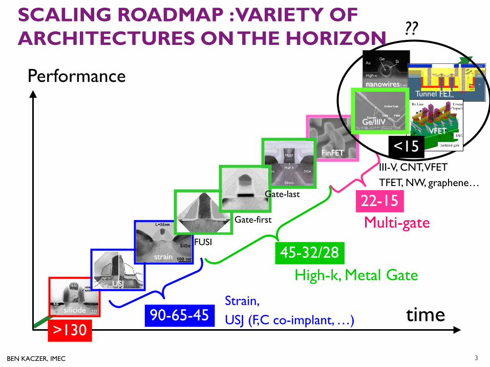
time
strain
USJ
silicide
>130 90-65-45
Strain, USJ (F,C co-implant, …)
Performance
22-15
FinFET
Multi-gate
45-32/28 High-k, Metal Gate
FUSI
Gate-first
Gate-last
??
Ge/IIIV
III-V, CNT, VFET TFET, NW, graphene…
nanowires Tunnel FET
<15 VFET
SCALING ROADMAP : VARIETY OF ARCHITECTURES ON THE HORIZON
BEN KACZER, IMEC
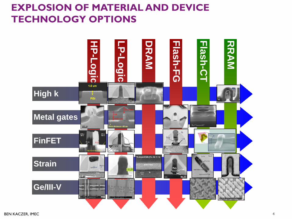
EXPLOSION OF MATERIAL AND DEVICE TECHNOLOGY OPTIONS
4
Ge/III-V
Strain
Metal gates
FinFET
High k
HP-Logic
LP-Logic
Flash-FG
DR
AM
RR
AM
Flash-CT
BEN KACZER, IMEC BEN KACZER, IMEC
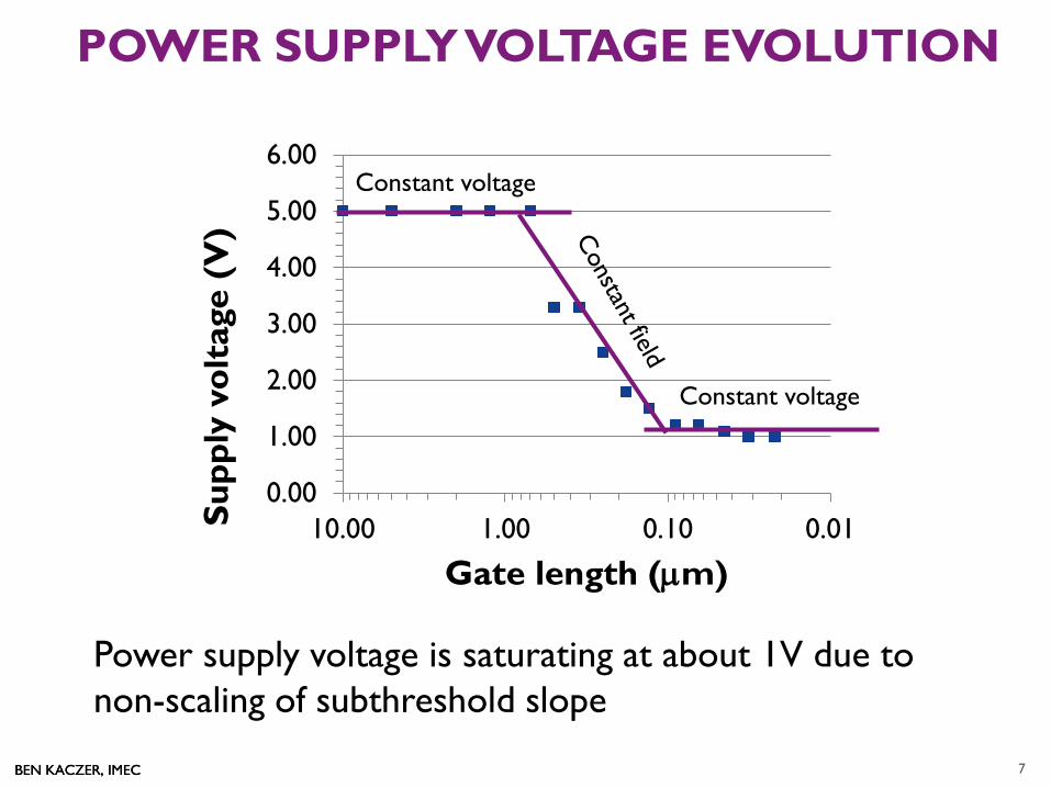
POWER SUPPLY VOLTAGE EVOLUTION
0.00
1.00
2.00
3.00
4.00
5.00
6.00
0.010.101.0010.00Supp
ly v
olta
ge (
V)
Gate length (µm)
Power supply voltage is saturating at about 1V due to non-scaling of subthreshold slope
Constant voltage
Constant voltage
7
BEN KACZER, IMEC
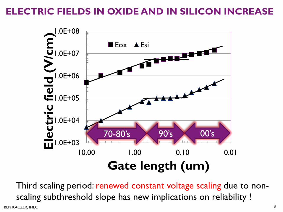
ELECTRIC FIELDS IN OXIDE AND IN SILICON INCREASE
Third scaling period: renewed constant voltage scaling due to non-scaling subthreshold slope has new implications on reliability !
8
1.0E+03
1.0E+04
1.0E+05
1.0E+06
1.0E+07
1.0E+08
0.010.101.0010.00
Ele
ctri
c fie
ld (
V/c
m)
Gate length (um)
Eox Esi
70-80’s 90’s 00’s
BEN KACZER, IMEC BEN KACZER, IMEC
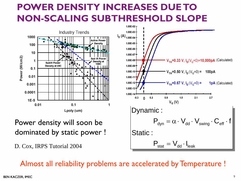
POWER DENSITY INCREASES DUE TO NON-SCALING SUBTHRESHOLD SLOPE
Power density will soon be dominated by static power !
leakddstat
effswingdddyn
IVP:Static
fCVVP:Dynamic
⋅=
⋅⋅⋅⋅α=
Almost all reliability problems are accelerated by Temperature !
D. Cox, IRPS Tutorial 2004
9
BEN KACZER, IMEC
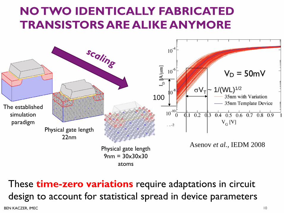
NO TWO IDENTICALLY FABRICATED TRANSISTORS ARE ALIKE ANYMORE
These time-zero variations require adaptations in circuit design to account for statistical spread in device parameters
10
The established simulation paradigm
Physical gate length 22nm
Physical gate length 9nm = 30x30x30
atoms
100
Asenov et al., IEDM 2008
σVT ~ 1/(WL)1/2
BEN KACZER, IMEC BEN KACZER, IMEC
OUTLINE
CMOS FEOL trends
Why reliability
Examples of FET degradation mechanisms
TDDB
BTI
11 BEN KACZER
BEN KACZER, IMEC BEN KACZER, IMEC
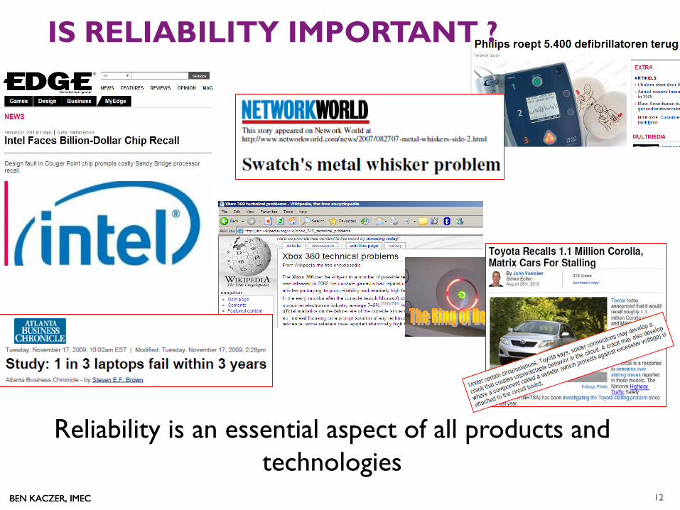
Reliability is an essential aspect of all products and technologies
12
IS RELIABILITY IMPORTANT ?
BEN KACZER, IMEC BEN KACZER, IMEC
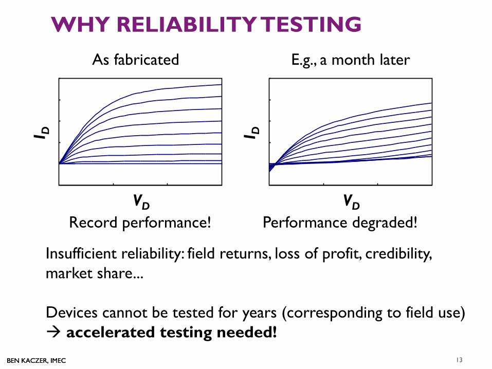
WHY RELIABILITY TESTING As fabricated
Record performance!
Insufficient reliability: field returns, loss of profit, credibility, market share... Devices cannot be tested for years (corresponding to field use) accelerated testing needed!
VD
I D
E.g., a month later
Performance degraded! VD
I D
13
BEN KACZER, IMEC BEN KACZER, IMEC
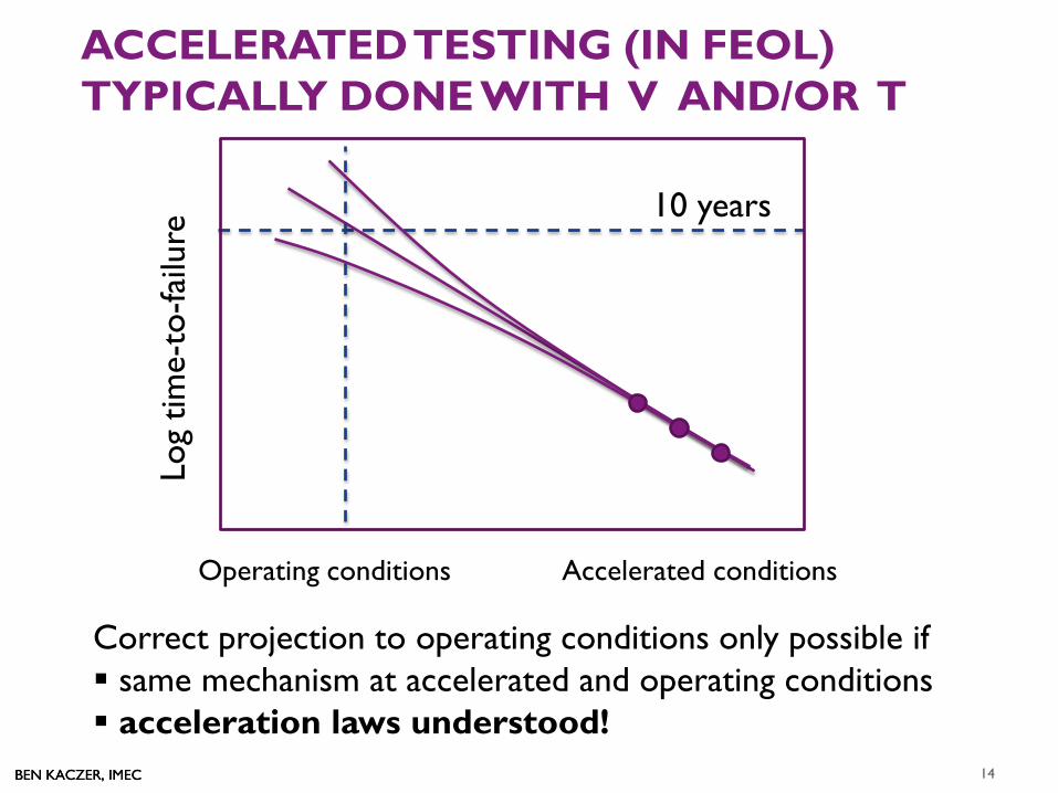
ACCELERATED TESTING (IN FEOL) TYPICALLY DONE WITH V AND/OR T
Operating conditions Accelerated conditions
Log
time-
to-fa
ilure
10 years
Correct projection to operating conditions only possible if same mechanism at accelerated and operating conditions acceleration laws understood!
14
BEN KACZER, IMEC BEN KACZER, IMEC
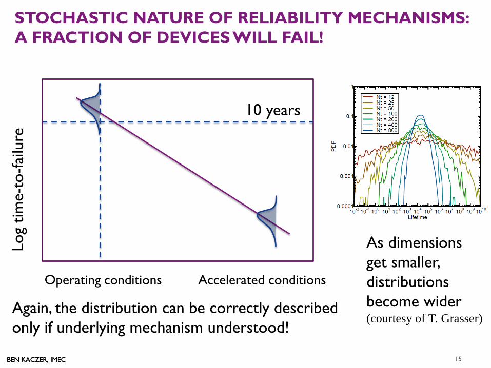
STOCHASTIC NATURE OF RELIABILITY MECHANISMS: A FRACTION OF DEVICES WILL FAIL!
Operating conditions Accelerated conditions
Log
time-
to-fa
ilure
10 years
Again, the distribution can be correctly described only if underlying mechanism understood!
As dimensions get smaller, distributions become wider (courtesy of T. Grasser)
15
BEN KACZER, IMEC BEN KACZER, IMEC 16
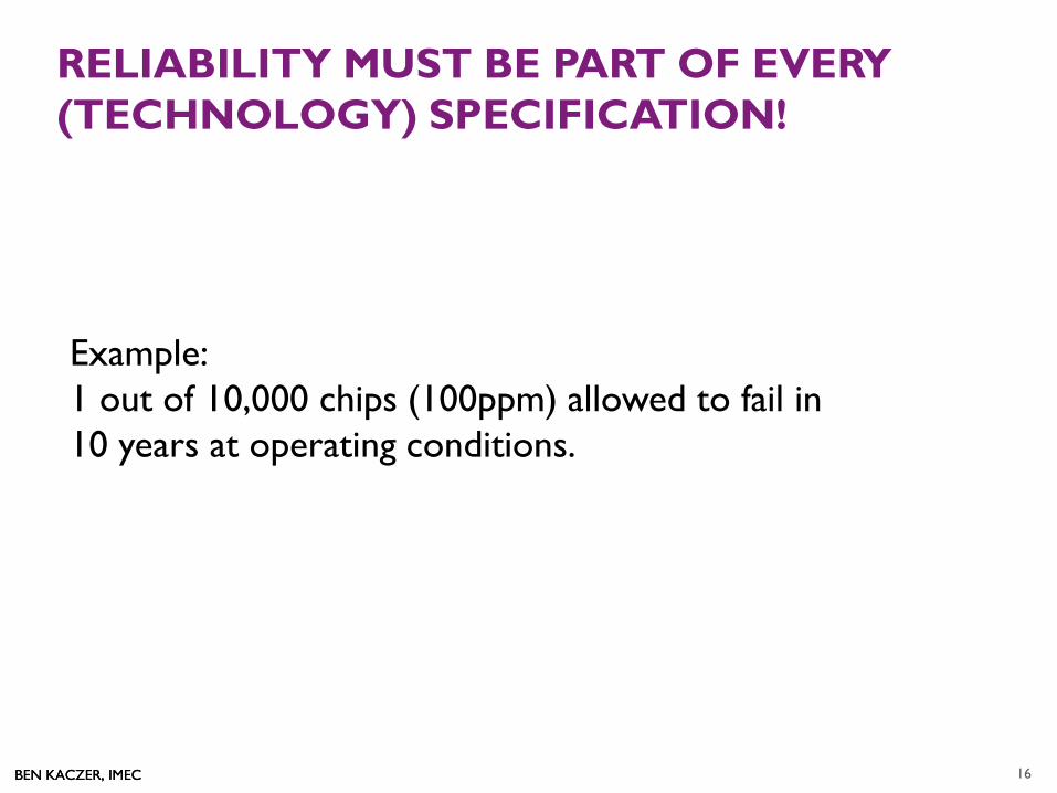
RELIABILITY MUST BE PART OF EVERY (TECHNOLOGY) SPECIFICATION!
Example: 1 out of 10,000 chips (100ppm) allowed to fail in 10 years at operating conditions.
BEN KACZER, IMEC BEN KACZER, IMEC
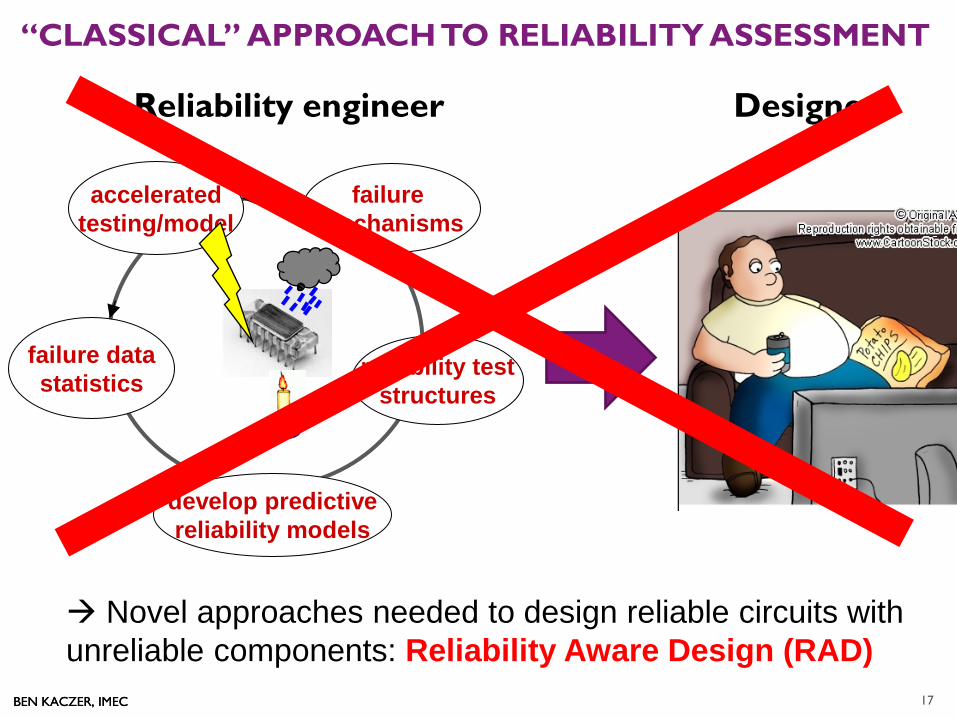
“CLASSICAL” APPROACH TO RELIABILITY ASSESSMENT
failure data statistics
develop predictive reliability models
accelerated testing/model
reliability test structures
failure mechanisms
Reliability engineer Designer
Novel approaches needed to design reliable circuits with unreliable components: Reliability Aware Design (RAD)
17
BEN KACZER, IMEC
RELIABILITY AND RECENT CMOS FEOL TRENDS • New (3D) device architectures • New “exotic” materials (high-k gate dielectrics, metal gates, high-mobility substrates)
• Downscaling of devices toward atomic dimensions (variability) • Supply voltages are not correspondingly reduced Reexamination of known “old” degradation mechanisms in new materials and architectures required Revision of existing and need for novel characterization techniques New reliability lifetime assessment methodologies Reliability cannot be guaranteed at technology level: Reliability-Aware Design
18
BEN KACZER, IMEC BEN KACZER, IMEC
OUTLINE
CMOS FEOL trends
Why reliability
Examples of FET degradation mechanisms
TDDB
BTI
19
BEN KACZER, IMEC BEN KACZER, IMEC
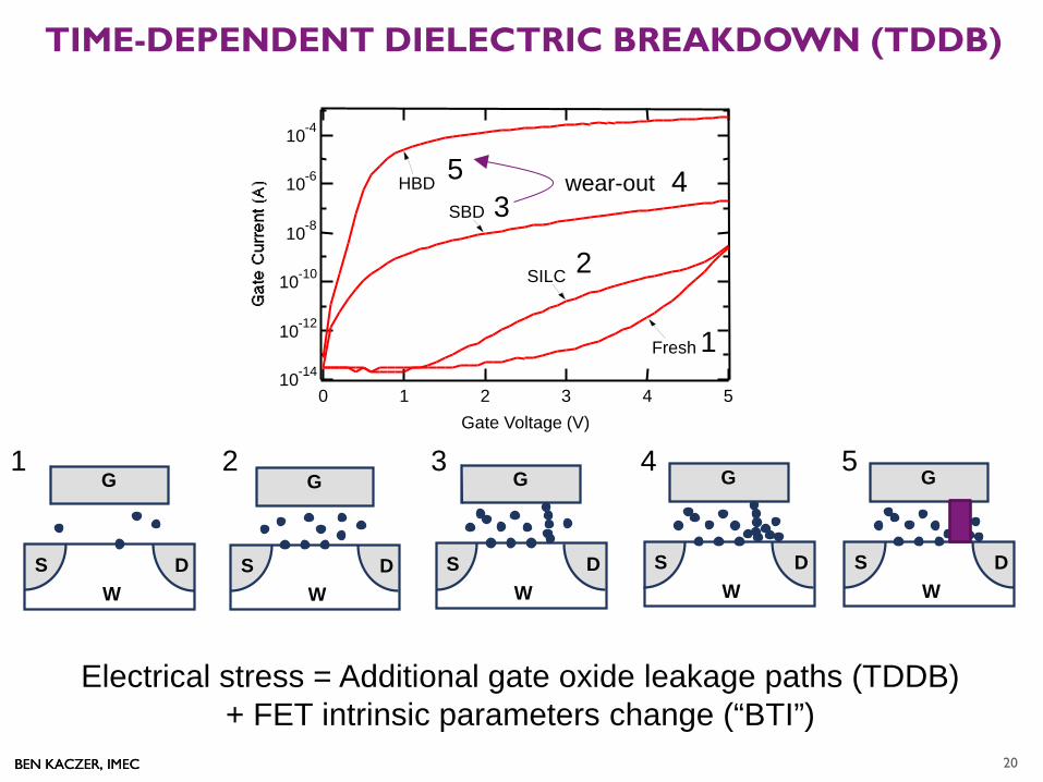
TIME-DEPENDENT DIELECTRIC BREAKDOWN (TDDB)
Electrical stress = Additional gate oxide leakage paths (TDDB) + FET intrinsic parameters change (“BTI”)
G
S DW
G
S DW
G
S DW
G
S DW
G
S DW
1
2
3 5
1 2 3 4 5
wear-out 4
20
10 -14
10 -12
10 -10
10 -8
10 -6
10 -4
5 4 3 2 1 0 Gate Voltage (V)
Fresh
SILC
SBD HBD
BEN KACZER, IMEC
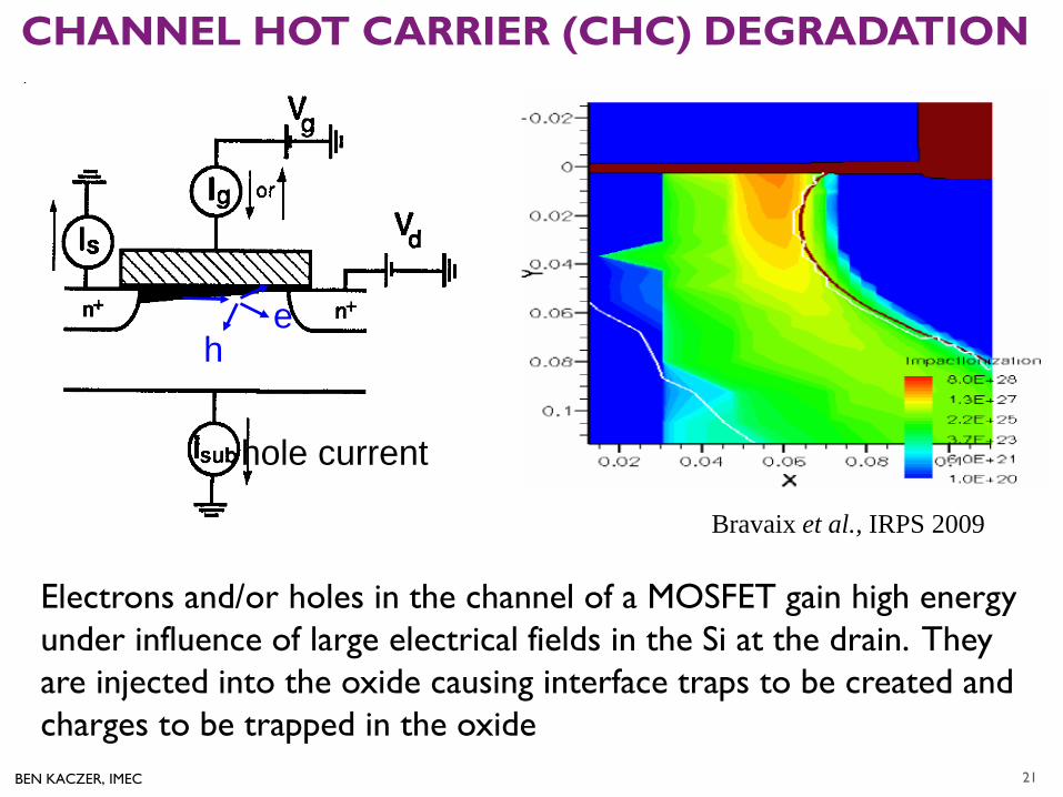
CHANNEL HOT CARRIER (CHC) DEGRADATION
21
h e
hole current
Electrons and/or holes in the channel of a MOSFET gain high energy under influence of large electrical fields in the Si at the drain. They are injected into the oxide causing interface traps to be created and charges to be trapped in the oxide
Bravaix et al., IRPS 2009
BEN KACZER, IMEC BEN KACZER, IMEC
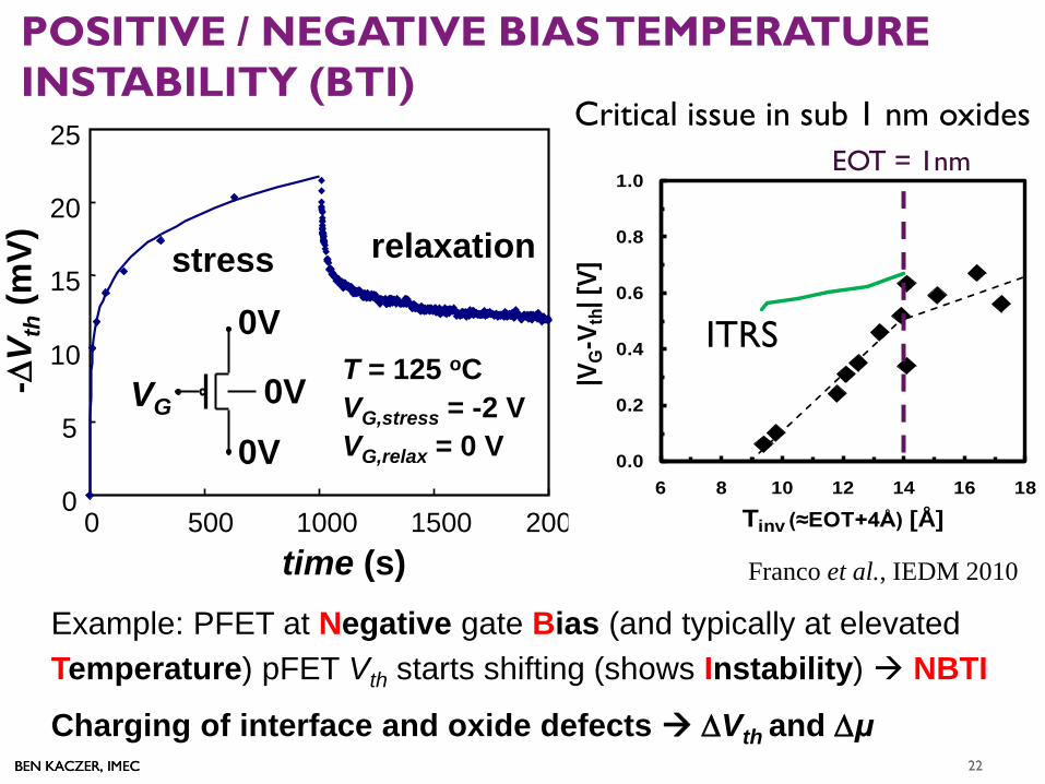
POSITIVE / NEGATIVE BIAS TEMPERATURE INSTABILITY (BTI)
0
5
10
15
20
25
0 500 1000 1500 2000 time (s)
-∆V t
h (m
V)
T = 125 oC VG,stress = -2 V VG,relax = 0 V
stress relaxation
0V
0V
0V VG
22
Example: PFET at Negative gate Bias (and typically at elevated Temperature) pFET Vth starts shifting (shows Instability) NBTI
Charging of interface and oxide defects ∆Vth and ∆μ
0.0
0.2
0.4
0.6
0.8
1.0
6 8 10 12 14 16 18
|VG-V
th| [
V]
Tinv (≈EOT+4Å) [Å]
EOT = 1nm
SiGe
Franco et al., IEDM 2010
ITRS
Critical issue in sub 1 nm oxides
BEN KACZER, IMEC BEN KACZER, IMEC
OUTLINE
CMOS FEOL trends
Why reliability
Examples of FET degradation mechanisms
TDDB • Overview / Phases of BD
• SILC • SBD & impact of position • Wear-out and HBD
BTI
23
BEN KACZER, IMEC 24 BEN KACZER, IMEC
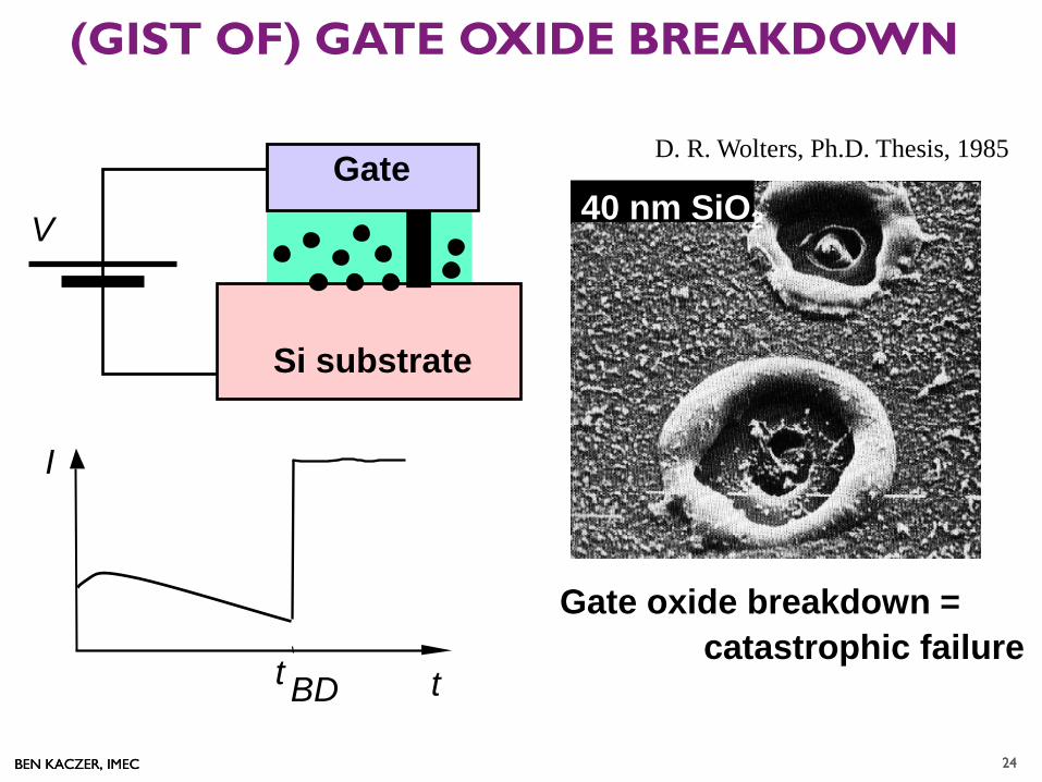
V
Gate
Si substrate
(GIST OF) GATE OXIDE BREAKDOWN
I
t t BD
D. R. Wolters, Ph.D. Thesis, 1985
40 nm SiO2
Gate oxide breakdown = catastrophic failure
24
BEN KACZER, IMEC BEN KACZER, IMEC
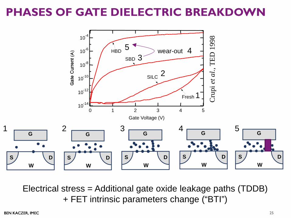
PHASES OF GATE DIELECTRIC BREAKDOWN
Electrical stress = Additional gate oxide leakage paths (TDDB) + FET intrinsic parameters change (“BTI”)
G
S DW
G
S DW
G
S DW
G
S DW
G
S DW
1
2
3 5
1 2 3 4 5
wear-out 4
10 -14
10 -12
10 -10
10 -8
10 -6
10 -4
5 4 3 2 1 0 Gate Voltage (V)
Fresh
SILC
SBD HBD
Cru
pi e
t al.,
TED
199
8 25
BEN KACZER, IMEC 26 BEN KACZER, IMEC
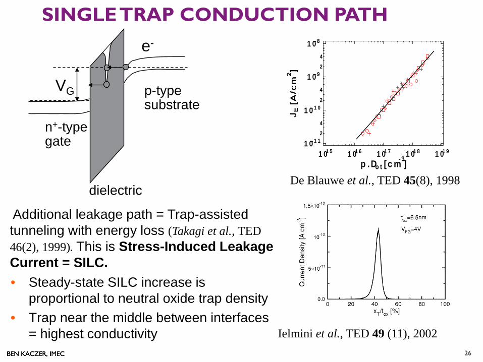
SINGLE TRAP CONDUCTION PATH
Additional leakage path = Trap-assisted tunneling with energy loss (Takagi et al., TED 46(2), 1999). This is Stress-Induced Leakage Current = SILC.
e-
VG
n+-type gate
p-type substrate
dielectric
1 0- 1 12
4
1 0- 1 02
4
1 0- 92
4
1 0- 8
1 01 5 1 01 6 1 01 7 1 01 8 1 01 9
p .Do t [c m-3]
Ielmini et al., TED 49 (11), 2002
• Steady-state SILC increase is proportional to neutral oxide trap density
• Trap near the middle between interfaces = highest conductivity
De Blauwe et al., TED 45(8), 1998
26
BEN KACZER, IMEC 27 BEN KACZER, IMEC
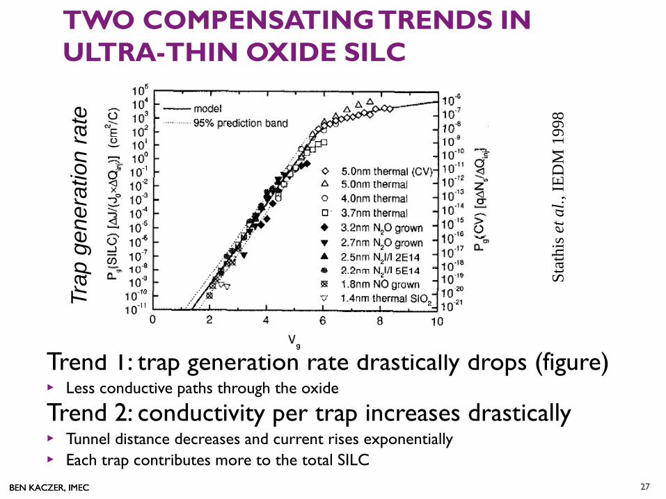
TWO COMPENSATING TRENDS IN ULTRA-THIN OXIDE SILC
Trend 1: trap generation rate drastically drops (figure) ▸ Less conductive paths through the oxide
Trend 2: conductivity per trap increases drastically ▸ Tunnel distance decreases and current rises exponentially ▸ Each trap contributes more to the total SILC
Stat
his e
t al.,
IED
M 1
998
Trap
gen
erat
ion
rate
27
BEN KACZER, IMEC 28 BEN KACZER, IMEC
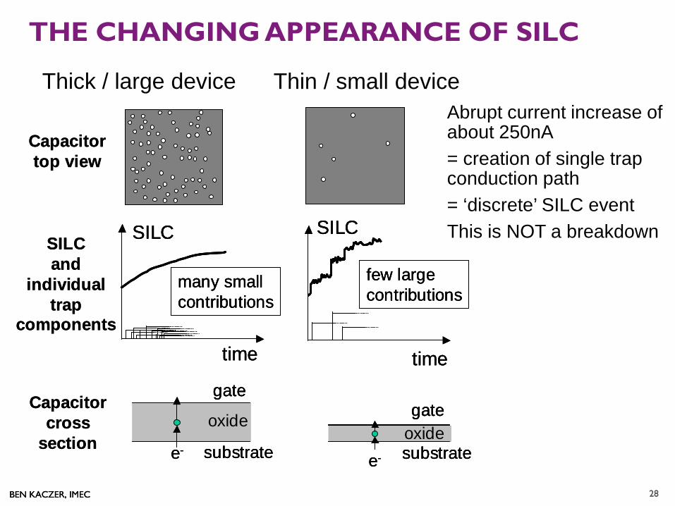
THE CHANGING APPEARANCE OF SILC
SILC
time
many smallcontributions
oxide
gate
substratee-
SILC
time
few largecontributions
oxidegate
substratee-
Capacitortop view
SILC and
individual trap
components
Capacitorcross
section
SILC
time
many smallcontributions
SILC
time
many smallcontributions
oxide
gate
substratee-
oxide
gate
substratee-
SILC
time
few largecontributions
SILC
time
few largecontributions
oxidegate
substratee-
oxidegate
substratee-
Capacitortop view
SILC and
individual trap
components
Capacitorcross
section
Thick / large device Thin / small device Abrupt current increase of about 250nA = creation of single trap conduction path = ‘discrete’ SILC event This is NOT a breakdown
28
BEN KACZER, IMEC 29 BEN KACZER, IMEC
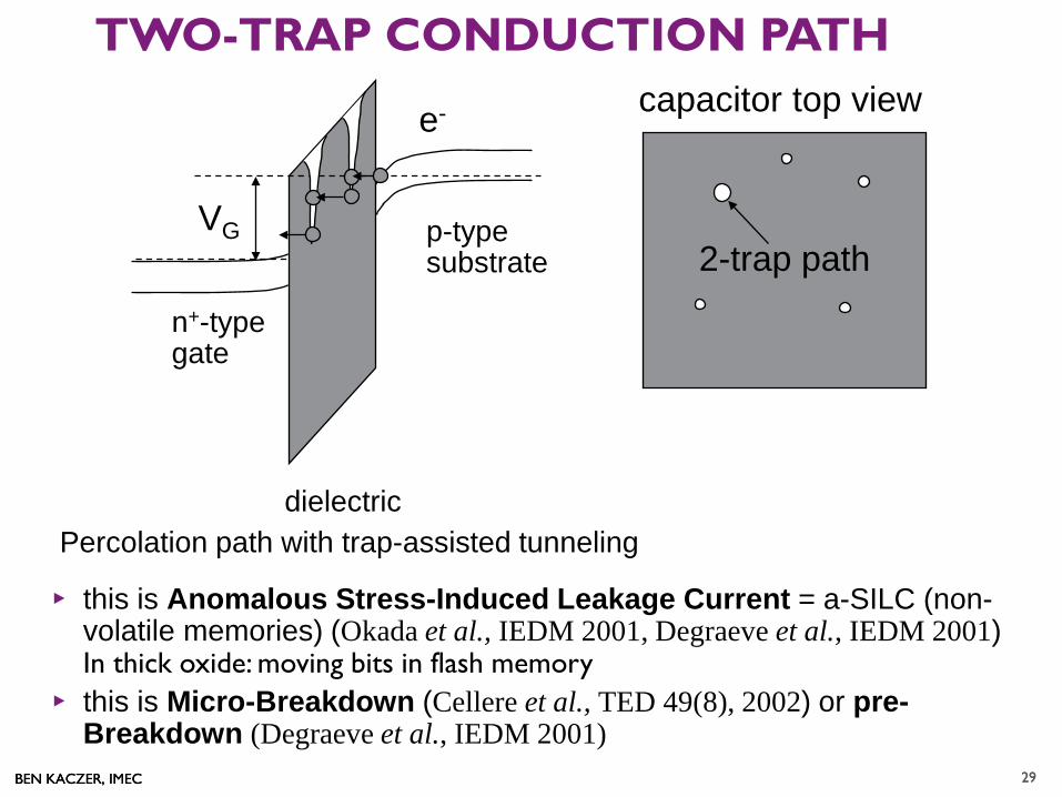
TWO-TRAP CONDUCTION PATH
Percolation path with trap-assisted tunneling
▸ this is Anomalous Stress-Induced Leakage Current = a-SILC (non-volatile memories) (Okada et al., IEDM 2001, Degraeve et al., IEDM 2001) In thick oxide: moving bits in flash memory
▸ this is Micro-Breakdown (Cellere et al., TED 49(8), 2002) or pre-Breakdown (Degraeve et al., IEDM 2001)
2-trap path
capacitor top view e-
VG
n+-type gate
p-type substrate
dielectric
29
BEN KACZER, IMEC BEN KACZER, IMEC
OUTLINE
CMOS FEOL trends
Why reliability
Examples of FET degradation mechanisms
TDDB • Overview / Phases of BD
• SILC • SBD & impact of position • Wear-out and HBD
BTI
30
BEN KACZER, IMEC 31 BEN KACZER, IMEC
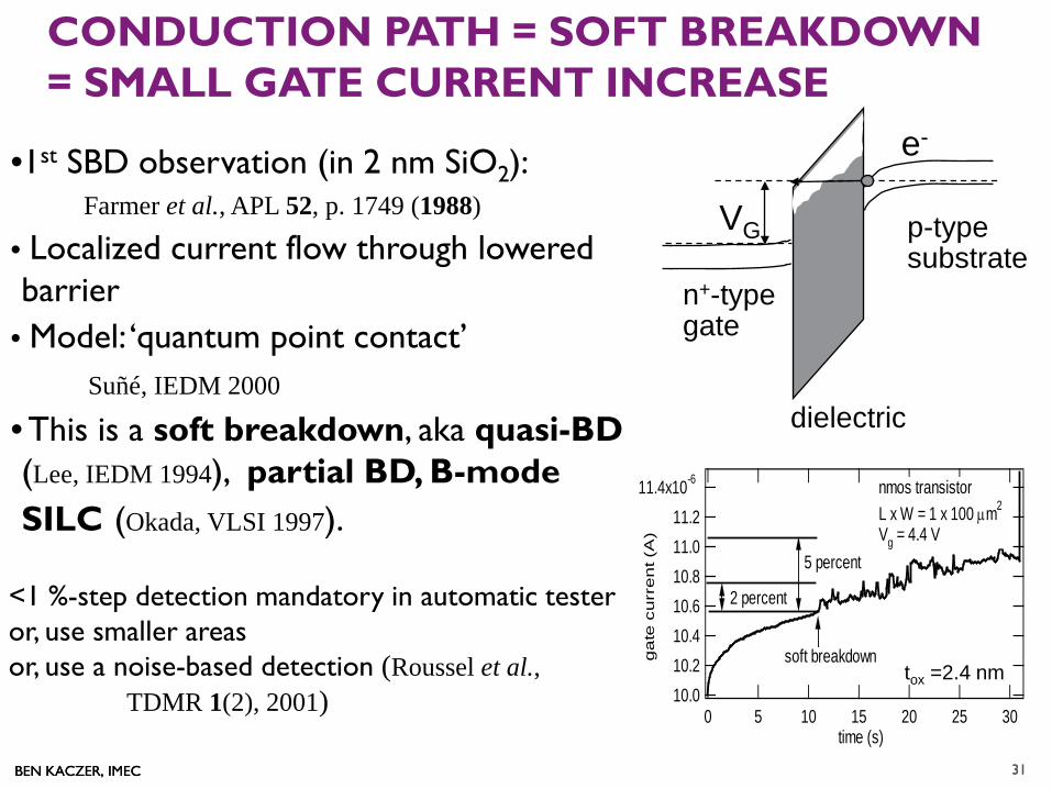
CONDUCTION PATH = SOFT BREAKDOWN = SMALL GATE CURRENT INCREASE
•1st SBD observation (in 2 nm SiO2): Farmer et al., APL 52, p. 1749 (1988)
• Localized current flow through lowered barrier
• Model: ‘quantum point contact’ Suñé, IEDM 2000
• This is a soft breakdown, aka quasi-BD (Lee, IEDM 1994), partial BD, B-mode SILC (Okada, VLSI 1997).
e-
VG
n+-type gate
p-type substrate
dielectric
<1 %-step detection mandatory in automatic tester or, use smaller areas or, use a noise-based detection (Roussel et al., TDMR 1(2), 2001)
11.4x10⁻⁶ 11.211.010.810.610.410.210.0
ga
te c
urr
en
t (A
)
302520151050time (s)
2 percent
5 percent
soft breakdown
nmos transistorL x W = 1 x 100 µm2
Vg = 4.4 V
tox =2.4 nm
31
BEN KACZER, IMEC BEN KACZER, IMEC
0
40
80
120
0 0.5 1.0 1.5 VD (V)
I D (µ
A)
G
S D W
Weff = 120 nm VG = 0, 0.15 .. 1.5 V
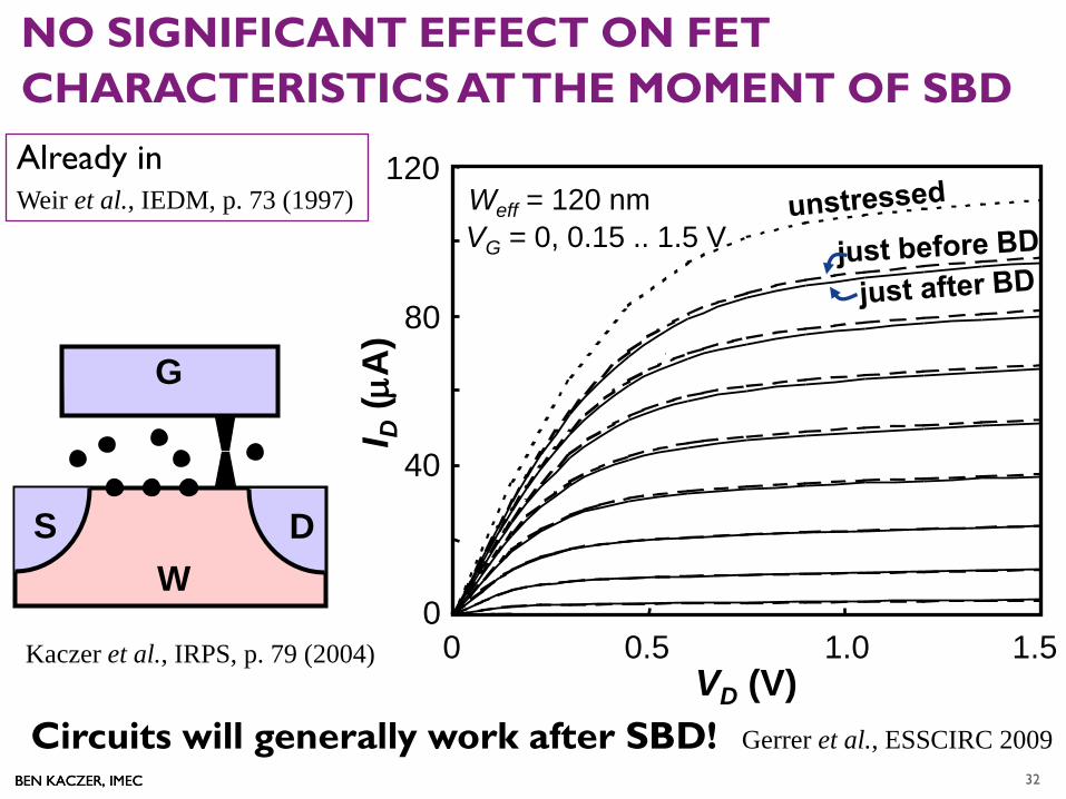
NO SIGNIFICANT EFFECT ON FET CHARACTERISTICS AT THE MOMENT OF SBD
Kaczer et al., IRPS, p. 79 (2004)
32
Already in Weir et al., IEDM, p. 73 (1997)
Circuits will generally work after SBD! Gerrer et al., ESSCIRC 2009

BEN KACZER, IMEC BEN KACZER, IMEC
TIME-TO-SOFT BREAKDOWN = STATISTICALLY DISTRIBUTED PARAMETER
Time-to-breakdown is Weibull distributed Monomodal Weibull distribution is described as:
( ) ( )( ) ( ) ( )ηβ−β=−−⇒
η
−−=β
lntlnF1lnlntexp1tF
-4-3-2-101
ln(-l
n(1-
F))
102 3 4 5 6 7
1002 3 4 5 6 7
1000tBD (s)
VG=4.4V
A=1.5e-08cm2
T=298CEOT=2.4nm
η=63%-value
β=slope
33
-5
-4
-3
-2
-1
0
1
ln(-ln
(1-F
))
0.012 4 6 8
0.12 4 6 8
1normalized Q BD
4.6 117.5
tox= 2.4 nm 3.4
-5
-4
-3
-2
-1
0
1
ln(-ln
(1-F
))
0.012 4 6 8
0.12 4 6 8
1normalized Q BD
4.6 117.5
tox= 2.4 nm 3.4
-5
-4
-3
-2
-1
0
1
ln(-ln
(1-F
))
-5
-4
-3
-2
-1
0
1
ln(-ln
(1-F
))
0.012 4 6 8
0.12 4 6 8
1normalized Q BD
4.64.6 11117.57.5
tox= 2.4 nmtox= 2.4 nm 3.43.4
dttJQ BDt
GBD ∫= 0)(
BEN KACZER, IMEC BEN KACZER, IMEC 34
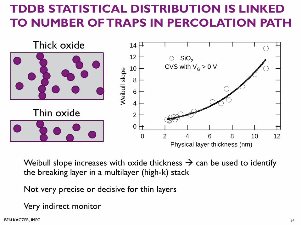
TDDB STATISTICAL DISTRIBUTION IS LINKED TO NUMBER OF TRAPS IN PERCOLATION PATH
Weibull slope increases with oxide thickness can be used to identify the breaking layer in a multilayer (high-k) stack
Not very precise or decisive for thin layers
Very indirect monitor
14
12
10
8
6
4
2
0W
eibu
ll sl
ope
121086420Physical layer thickness (nm)
SiO2CVS with VG > 0 V
Thick oxide
Thin oxide
BEN KACZER, IMEC 35 BEN KACZER, IMEC 35
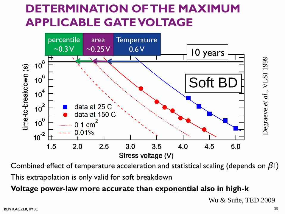
DETERMINATION OF THE MAXIMUM APPLICABLE GATE VOLTAGE
Combined effect of temperature acceleration and statistical scaling (depends on β!) This extrapolation is only valid for soft breakdown Voltage power-law more accurate than exponential also in high-k Wu & Suñe, TED 2009
Soft BD
Deg
raev
e et
al.,
VLS
I 199
9
Temperature 0.6 V
percentile ~0.3 V
area ~0.25 V 10 years
BEN KACZER, IMEC BEN KACZER, IMEC
G
S D W
G
S D W
G
S D W
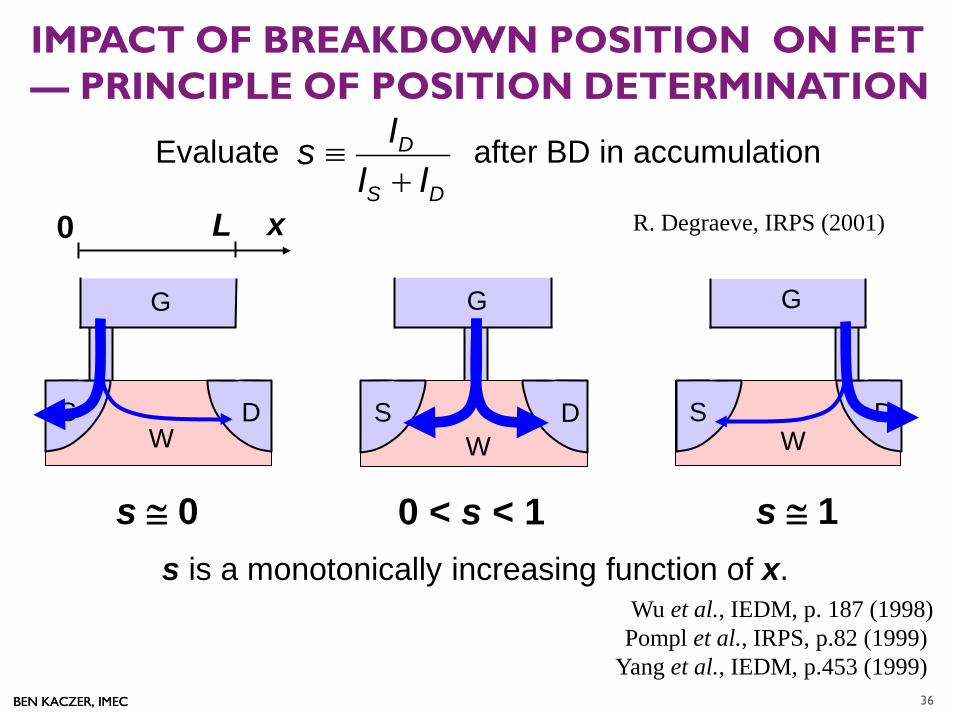
0 L x
s is a monotonically increasing function of x.
R. Degraeve, IRPS (2001)
0 < s < 1 s ≅ 0 s ≅ 1
IMPACT OF BREAKDOWN POSITION ON FET — PRINCIPLE OF POSITION DETERMINATION
DS
D
IIIs+
≡Evaluate after BD in accumulation
Wu et al., IEDM, p. 187 (1998) Pompl et al., IRPS, p.82 (1999)
Yang et al., IEDM, p.453 (1999) 36
BEN KACZER, IMEC BEN KACZER, IMEC
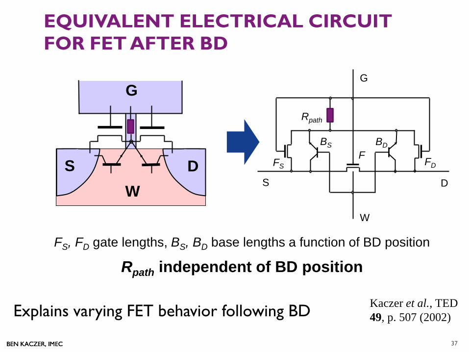
EQUIVALENT ELECTRICAL CIRCUIT FOR FET AFTER BD
37
D S
W
G
FS
Rpath
BS
FD
BD F
FS, FD gate lengths, BS, BD base lengths a function of BD position
Rpath independent of BD position
G
S D W
Explains varying FET behavior following BD Kaczer et al., TED 49, p. 507 (2002)
BEN KACZER, IMEC BEN KACZER, IMEC 38
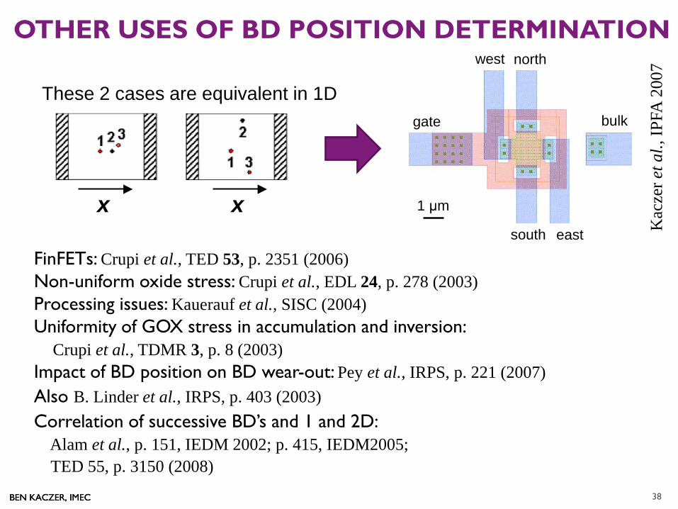
OTHER USES OF BD POSITION DETERMINATION
FinFETs: Crupi et al., TED 53, p. 2351 (2006) Non-uniform oxide stress: Crupi et al., EDL 24, p. 278 (2003) Processing issues: Kauerauf et al., SISC (2004) Uniformity of GOX stress in accumulation and inversion: Crupi et al., TDMR 3, p. 8 (2003) Impact of BD position on BD wear-out: Pey et al., IRPS, p. 221 (2007) Also B. Linder et al., IRPS, p. 403 (2003) Correlation of successive BD’s and 1 and 2D: Alam et al., p. 151, IEDM 2002; p. 415, IEDM2005; TED 55, p. 3150 (2008)
These 2 cases are equivalent in 1D
x x eastsouth
west north
gate bulk
1 μm
Kac
zer e
t al.,
IPFA
200
7
BEN KACZER, IMEC BEN KACZER, IMEC
OUTLINE
CMOS FEOL trends
Why reliability
Examples of FET degradation mechanisms
TDDB • Overview / Phases of BD
• SILC • SBD & impact of position • Wear-out and HBD
BTI
39
BEN KACZER, IMEC 40 BEN KACZER, IMEC
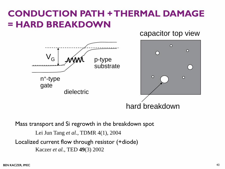
CONDUCTION PATH + THERMAL DAMAGE = HARD BREAKDOWN
Mass transport and Si regrowth in the breakdown spot Lei Jun Tang et al., TDMR 4(1), 2004
Localized current flow through resistor (+diode) Kaczer et al., TED 49(3) 2002
VG
n+-type gate
p-type substrate
dielectric
capacitor top view
hard breakdown
40
BEN KACZER, IMEC 41 BEN KACZER, IMEC
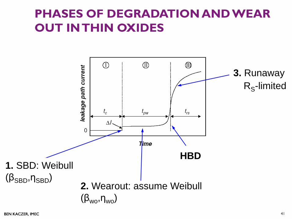
PHASES OF DEGRADATION AND WEAR OUT IN THIN OXIDES
1. SBD: Weibull (βSBD,ηSBD)
2. Wearout: assume Weibull (βwo,ηwo)
3. Runaway
HBD
RS-limited
41
BEN KACZER, IMEC 42 BEN KACZER, IMEC
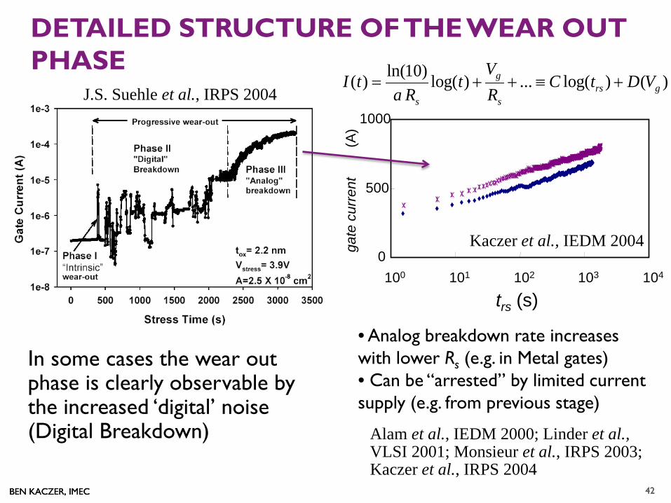
DETAILED STRUCTURE OF THE WEAR OUT PHASE
In some cases the wear out phase is clearly observable by the increased ‘digital’ noise (Digital Breakdown)
J.S. Suehle et al., IRPS 2004
Kaczer et al., IEDM 2004 0
500
1000
100 101 102 103 104
trs (s)
gate
cur
rent
(A
) • Analog breakdown rate increases with lower Rs (e.g. in Metal gates) • Can be “arrested” by limited current supply (e.g. from previous stage)
ln(10)( ) log( ) ... log( ) ( )grs g
s s
VI t t C t D V
a R R= + + ≡ +
Alam et al., IEDM 2000; Linder et al., VLSI 2001; Monsieur et al., IRPS 2003; Kaczer et al., IRPS 2004
42
BEN KACZER, IMEC 43 BEN KACZER, IMEC 43
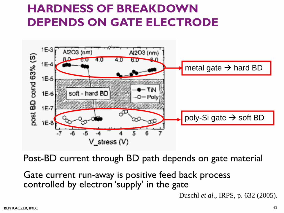
HARDNESS OF BREAKDOWN DEPENDS ON GATE ELECTRODE
Post-BD current through BD path depends on gate material
Gate current run-away is positive feed back process controlled by electron ‘supply’ in the gate
metal gate hard BD
poly-Si gate soft BD
Duschl et al., IRPS, p. 632 (2005).
BEN KACZER, IMEC 44 BEN KACZER, IMEC
-3
-2
-1
0
1
ln(-l
n(1-
F))
12 4 6
102 4 6
1002 4 6
1000time-to-breakdown (s)
VG=2.2V0.9 nm EOT SiO2/HfO2
A=1.25e-09cm2
HBD βHBD=~1.2SBD βSBD=~0.7
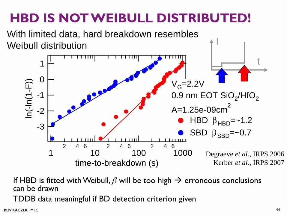
HBD IS NOT WEIBULL DISTRIBUTED!
If HBD is fitted with Weibull, β will be too high erroneous conclusions can be drawn
TDDB data meaningful if BD detection criterion given
t
I
44
With limited data, hard breakdown resembles Weibull distribution
Degraeve et al., IRPS 2006 Kerber et al., IRPS 2007
BEN KACZER, IMEC 45 BEN KACZER, IMEC
virgin device 1st SBD
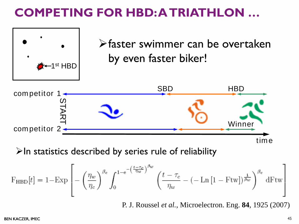
COMPETING FOR HBD: A TRIATHLON …
In statistics described by series rule of reliability
2nd SBD
3rd SBD
1st HBD
faster swimmer can be overtaken by even faster biker!
time
SBD HBD
STA
RT Winner
competitor 1
competitor 2
45
P. J. Roussel et al., Microelectron. Eng. 84, 1925 (2007)
BEN KACZER, IMEC 46 BEN KACZER, IMEC
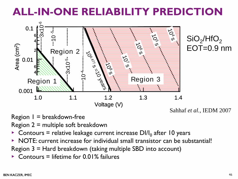
ALL-IN-ONE RELIABILITY PREDICTION
Region 1 = breakdown-free Region 2 = multiple soft breakdown ▸ Contours = relative leakage current increase DI/I0 after 10 years ▸ NOTE: current increase for individual small transistor can be substantial!
Region 3 = Hard breakdown (taking multiple SBD into account) ▸ Contours = lifetime for 0.01% failures
0.001
2
46
0.01
2
46
0.1
Area
(cm
2 )
1.41.31.21.11.0Voltage (V)
10 8.477 s =10 years10 8 s
10 7 s 10 6 s
10 5 s
10 4 s
Region 3Region 1
Region 23x
10-6
10- 43x
10-5
10-5
0.001
2
46
0.01
2
46
0.1
Area
(cm
2 )
1.41.31.21.11.0Voltage (V)
10 8.477 s =10 years10 8 s
10 7 s 10 6 s
10 5 s
10 4 s
Region 3Region 1
Region 23x
10-6
10- 43x
10-5
10-5
SiO2/HfO2 EOT=0.9 nm
46
Sahhaf et al., IEDM 2007
BEN KACZER, IMEC BEN KACZER, IMEC
OUTLINE CMOS FEOL trends
Why reliability
Examples of FET degradation mechanisms
TDDB
BTI • Overview / BTI components
• Technological remedies
• NBTI recoverable component and AC stress
• BTI in deeply scaled devices
• Observing properties of individual defects
• Impact of individual defects on FET characteristics
• Constructing and projecting ∆Vth distributions
• Combining time-dependent and time-0 variabilities
• Defect-centric circuit simulation framework
47
BEN KACZER, IMEC 48 BEN KACZER, IMEC
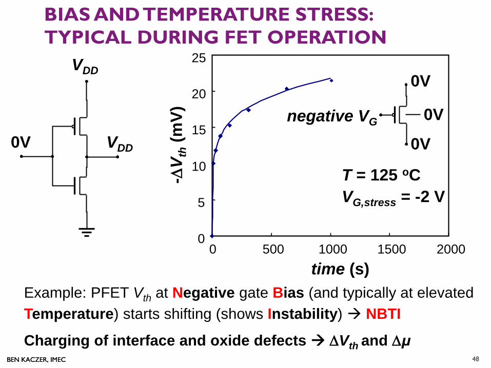
BIAS AND TEMPERATURE STRESS: TYPICAL DURING FET OPERATION
VDD
0V VDD
0
5
10
15
20
25
0 500 1000 1500 2000 time (s)
-∆V t
h (m
V)
T = 125 oC VG,stress = -2 V
0V
0V
0V negative VG
Example: PFET Vth at Negative gate Bias (and typically at elevated Temperature) starts shifting (shows Instability) NBTI
Charging of interface and oxide defects ∆Vth and ∆μ 48
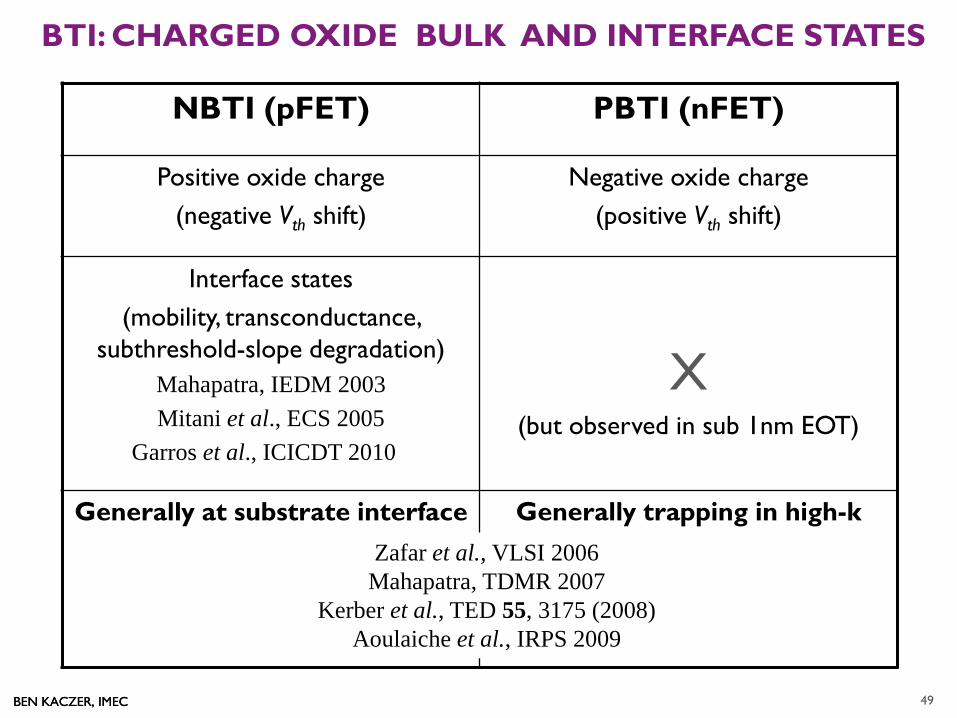
BEN KACZER, IMEC BEN KACZER, IMEC
NBTI (pFET) PBTI (nFET)
Positive oxide charge (negative Vth shift)
Negative oxide charge (positive Vth shift)
Interface states (mobility, transconductance,
subthreshold-slope degradation) Mahapatra, IEDM 2003 Mitani et al., ECS 2005
Garros et al., ICICDT 2010
X
(but observed in sub 1nm EOT)
Generally at substrate interface
Generally trapping in high-k
BTI: CHARGED OXIDE BULK AND INTERFACE STATES
49
Zafar et al., VLSI 2006 Mahapatra, TDMR 2007
Kerber et al., TED 55, 3175 (2008) Aoulaiche et al., IRPS 2009
BEN KACZER, IMEC 50 BEN KACZER, IMEC
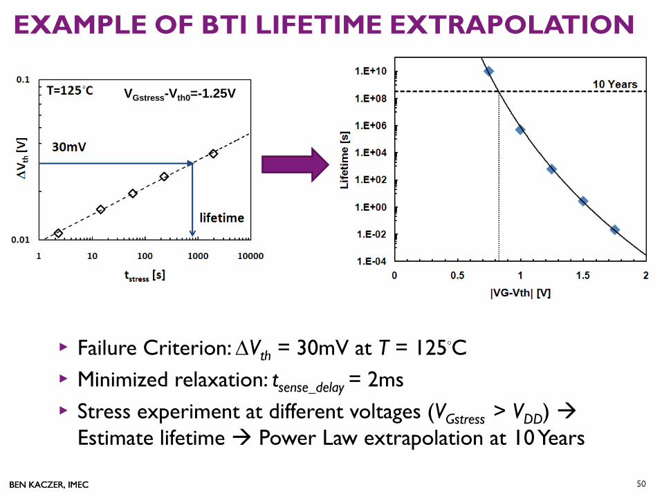
EXAMPLE OF BTI LIFETIME EXTRAPOLATION
▸ Failure Criterion: ∆Vth = 30mV at T = 125◦C ▸ Minimized relaxation: tsense_delay = 2ms ▸ Stress experiment at different voltages (VGstress > VDD)
Estimate lifetime Power Law extrapolation at 10 Years
50
VGstress-Vth0=-1.25V
BEN KACZER, IMEC 51 BEN KACZER, IMEC
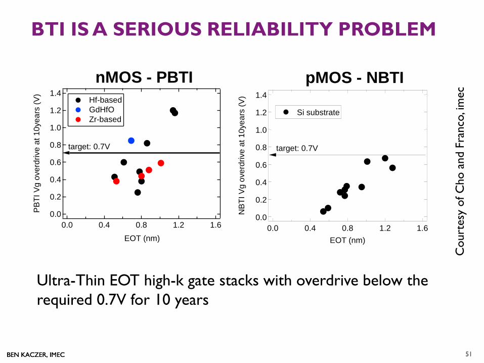
BTI IS A SERIOUS RELIABILITY PROBLEM
Ultra-Thin EOT high-k gate stacks with overdrive below the required 0.7V for 10 years
nMOS - PBTI pMOS - NBTI 1.4
1.2
1.0
0.8
0.6
0.4
0.2
0.0PB
TI V
g ov
erdr
ive
at 1
0yea
rs (V
)
1.61.20.80.40.0EOT (nm)
Hf-based GdHfO Zr-based
target: 0.7V
1.4
1.2
1.0
0.8
0.6
0.4
0.2
0.0 NB
TI V
g ov
erdr
ive
at 1
0yea
rs (V
) 1.6 1.2 0.8 0.4 0.0
EOT (nm)
target: 0.7V
Si substrate
51
Cou
rtes
y of
Cho
and
Fra
nco,
imec
BEN KACZER, IMEC BEN KACZER, IMEC
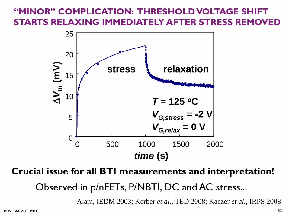
“MINOR” COMPLICATION: THRESHOLD VOLTAGE SHIFT STARTS RELAXING IMMEDIATELY AFTER STRESS REMOVED
0
5
10
15
20
25
0 500 1000 1500 2000 time (s)
∆V t
h (m
V)
T = 125 oC VG,stress = -2 V VG,relax = 0 V
stress relaxation
52
Crucial issue for all BTI measurements and interpretation!
Observed in p/nFETs, P/NBTI, DC and AC stress... Alam, IEDM 2003; Kerber et al., TED 2008; Kaczer et al., IRPS 2008
BEN KACZER, IMEC 54 BEN KACZER, IMEC
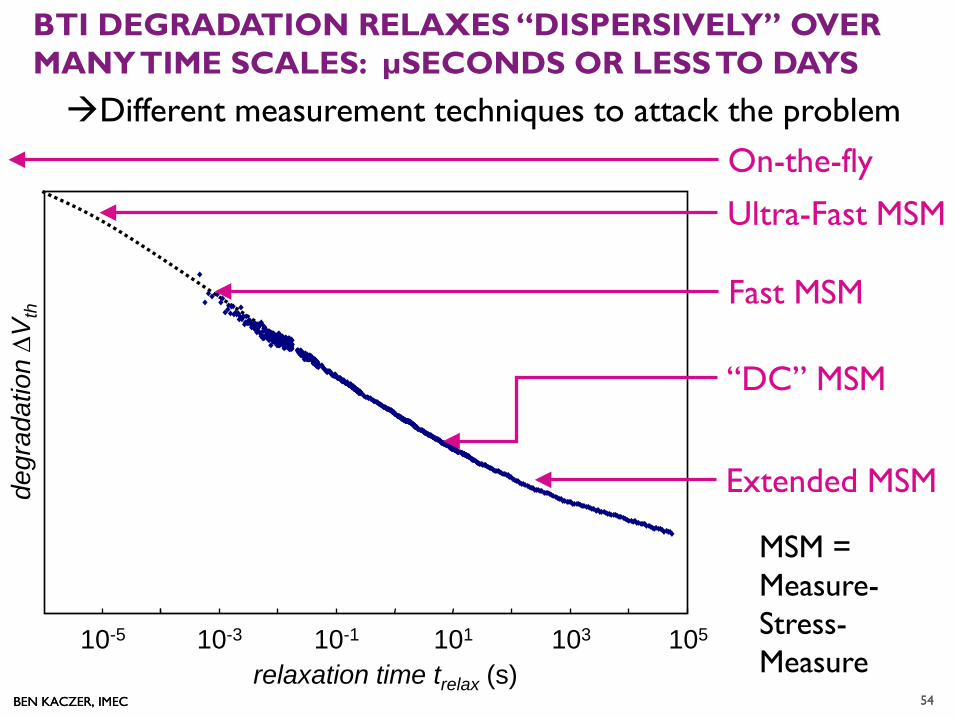
BTI DEGRADATION RELAXES “DISPERSIVELY” OVER MANY TIME SCALES: µSECONDS OR LESS TO DAYS
10-3 10-1 101 103 105
relaxation time trelax (s)
“DC” MSM
Fast MSM
Ultra-Fast MSM
On-the-fly
Extended MSM
Different measurement techniques to attack the problem
MSM = Measure-Stress-Measure
10-5
degr
adat
ion ∆V
th
54
BEN KACZER, IMEC BEN KACZER, IMEC
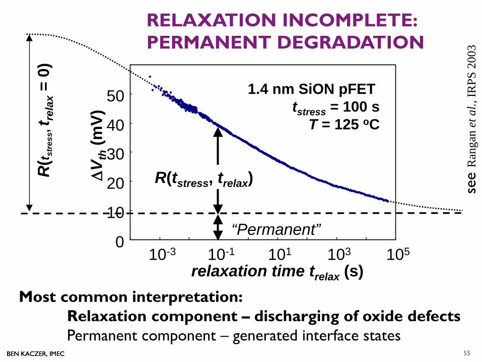
RELAXATION INCOMPLETE: PERMANENT DEGRADATION
0
10
20
30
40
50
10-3 10-1 101 103 105
relaxation time trelax (s)
∆V t
h (m
V)
“Permanent”
R(tstress, trelax) R(t s
tres
s, t re
lax =
0)
1.4 nm SiON pFET tstress = 100 s
T = 125 oC
Most common interpretation: Relaxation component – discharging of oxide defects Permanent component – generated interface states
55
see
Ran
gan
et a
l., IR
PS 2
003
BEN KACZER, IMEC BEN KACZER, IMEC
OUTLINE CMOS FEOL trends
Why reliability
Examples of FET degradation mechanisms
TDDB
BTI • Overview / BTI components
• Technological remedies
• NBTI recoverable component and AC stress
• BTI in deeply scaled devices
• Observing properties of individual defects
• Impact of individual defects on FET characteristics
• Constructing and projecting ∆Vth distributions
• Combining time-dependent and time-0 variabilities
• Defect-centric circuit simulation framework
60 BEN KACZER
BEN KACZER, IMEC BEN KACZER, IMEC
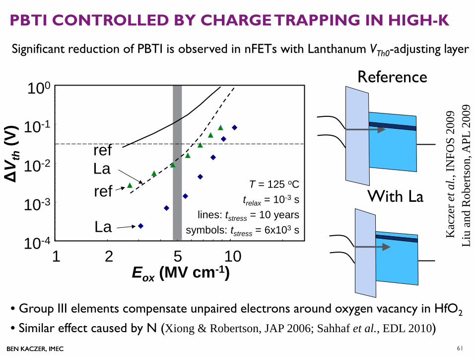
PBTI CONTROLLED BY CHARGE TRAPPING IN HIGH-K
10-4
10-3
10-2
10-1
100
1 Eox (MV cm-1)
ΔV t
h (V)
2 5 10
ref La ref
La
T = 125 oC trelax = 10-3 s
lines: tstress = 10 years symbols: tstress = 6x10³ s
• Group III elements compensate unpaired electrons around oxygen vacancy in HfO2
• Similar effect caused by N (Xiong & Robertson, JAP 2006; Sahhaf et al., EDL 2010)
Kac
zer e
t al.,
INFO
S 20
09
61
Reference
With La
Liu
and
Rob
erts
on, A
PL 2
009
Significant reduction of PBTI is observed in nFETs with Lanthanum VTh0-adjusting layer
BEN KACZER, IMEC 63 BEN KACZER, IMEC
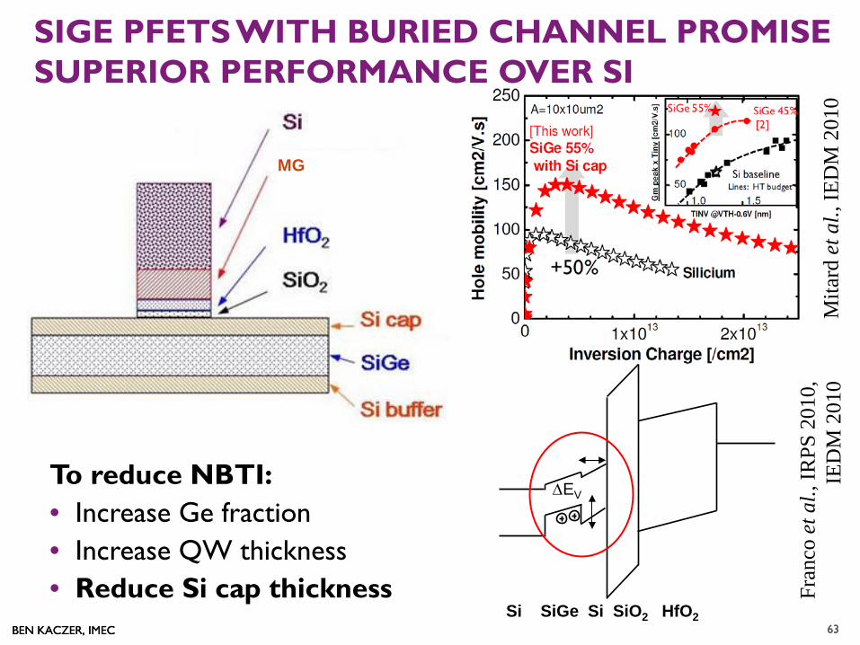
SIGE PFETS WITH BURIED CHANNEL PROMISE SUPERIOR PERFORMANCE OVER SI
∆EV
Si SiGe Si SiO2 HfO2
MG
63
To reduce NBTI: • Increase Ge fraction • Increase QW thickness • Reduce Si cap thickness Fr
anco
et a
l., IR
PS 2
010,
IE
DM
201
0 M
itard
et a
l., IE
DM
201
0
BEN KACZER, IMEC 64 BEN KACZER, IMEC
0
0.2
0.4
0.6
0.8
1
1.2
1.4
6 8 10 12 14 16 18
Max
. |V G
-Vth
| for
10Y
[V]
Tinv [Å]
Ultra-Thin EOT
0123456789
6 8 10 12 14 16 18 M
ax. E
ox fo
r 10Y
[MV/
cm]
Tinv [Å]
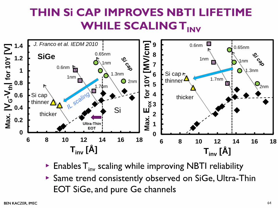
THIN Si CAP IMPROVES NBTI LIFETIME WHILE SCALING TINV
▸ Enables Tinv scaling while improving NBTI reliability ▸ Same trend consistently observed on SiGe, Ultra-Thin
EOT SiGe, and pure Ge channels
Si cap thinner
thicker
0.65nm
1nm
1.3nm 2nm
Si cap thinner
thicker
0.65nm
1.3nm
2nm
1nm SiGe
Si
0.6nm
1nm
1.7nm
0.6nm
1nm
1.7nm
J. Franco et al. IEDM 2010
64
BEN KACZER, IMEC 65 BEN KACZER, IMEC
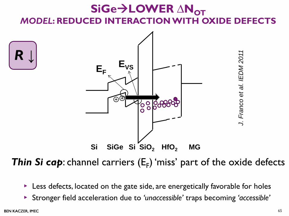
Thin Si cap: channel carriers (EF) ‘miss’ part of the oxide defects
SiGeLOWER ∆NOT MODEL: REDUCED INTERACTION WITH OXIDE DEFECTS
SiGe Si SiO2 HfO2 Si
EF EVS
MG
▸ Less defects, located on the gate side, are energetically favorable for holes ▸ Stronger field acceleration due to ‘unaccessible’ traps becoming ‘accessible’
R ↓
J. F
ranc
o et
al.
IED
M 2
011
65
BEN KACZER, IMEC 66 BEN KACZER, IMEC
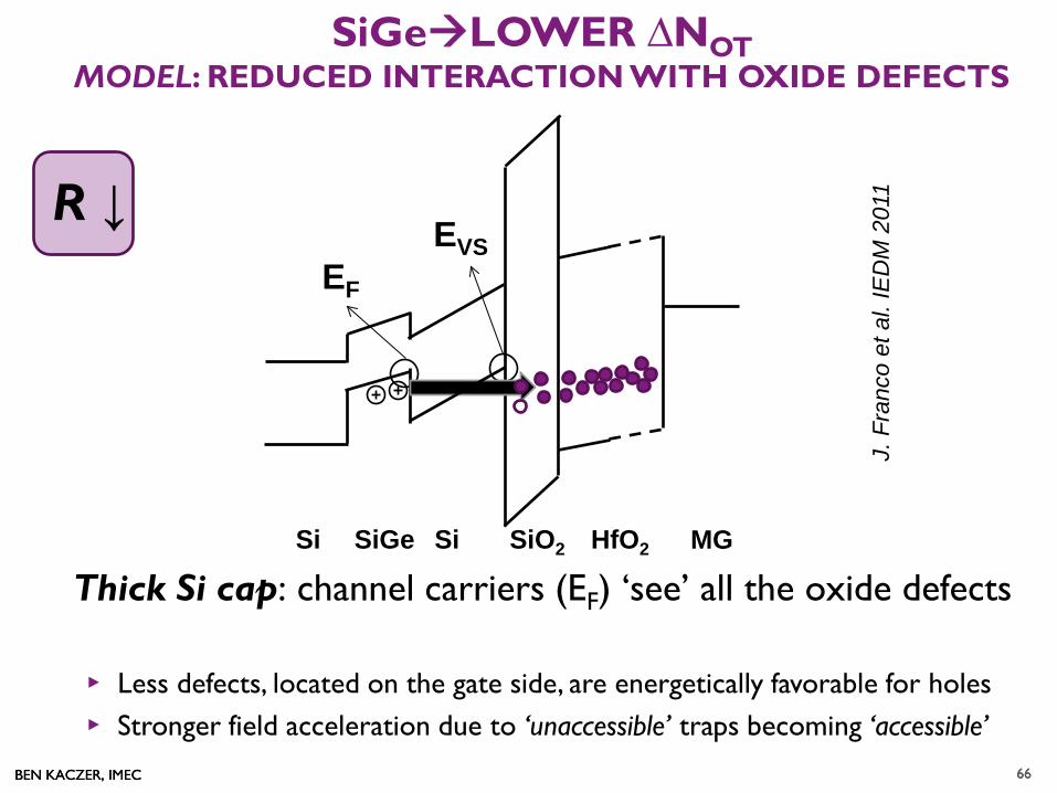
Thick Si cap: channel carriers (EF) ‘see’ all the oxide defects
EF
EVS
SiGe Si SiO2 HfO2 Si MG
SiGeLOWER ∆NOT MODEL: REDUCED INTERACTION WITH OXIDE DEFECTS
▸ Less defects, located on the gate side, are energetically favorable for holes ▸ Stronger field acceleration due to ‘unaccessible’ traps becoming ‘accessible’
R ↓
J. F
ranc
o et
al.
IED
M 2
011
66
BEN KACZER, IMEC 68 BEN KACZER, IMEC
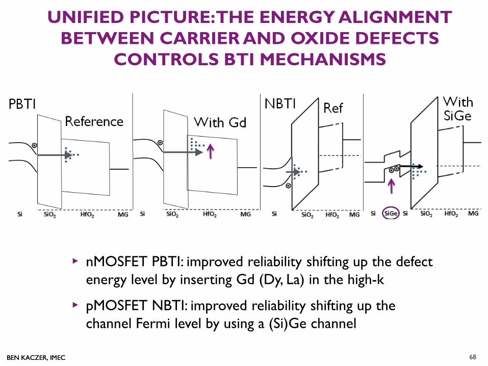
UNIFIED PICTURE: THE ENERGY ALIGNMENT BETWEEN CARRIER AND OXIDE DEFECTS
CONTROLS BTI MECHANISMS
▸ nMOSFET PBTI: improved reliability shifting up the defect energy level by inserting Gd (Dy, La) in the high-k
▸ pMOSFET NBTI: improved reliability shifting up the channel Fermi level by using a (Si)Ge channel
68

BEN KACZER, IMEC BEN KACZER, IMEC
OUTLINE CMOS FEOL trends
Why reliability
Examples of FET degradation mechanisms
TDDB
BTI • Overview / BTI components
• Technological remedies
• NBTI recoverable component and AC stress
• BTI in deeply scaled devices
• Observing properties of individual defects
• Impact of individual defects on FET characteristics
• Constructing and projecting ∆Vth distributions
• Combining time-dependent and time-0 variabilities
• Defect-centric circuit simulation framework
69
BEN KACZER, IMEC BEN KACZER, IMEC
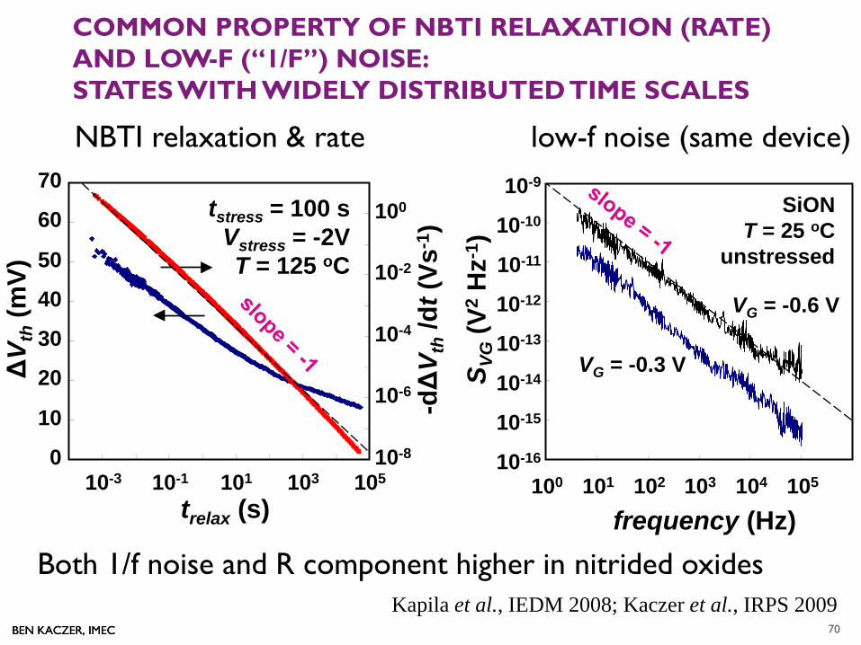
COMMON PROPERTY OF NBTI RELAXATION (RATE) AND LOW-F (“1/F”) NOISE: STATES WITH WIDELY DISTRIBUTED TIME SCALES
tstress = 100 s Vstress = -2V T = 125 oC
0
10
20
30
40
50
60
70
10-3 10-1 101 103 105 trelax (s)
ΔV t
h (m
V)
10-8
10-6
10-4
10-2
100
-dΔ
V th /
dt (V
s-1 )
10-16
10-15
10-14
10-13
10-12
10-11
10-10
10-9
100 101 102 103 104 105
frequency (Hz) S V
G (V
2 Hz-
1 )
SiON T = 25 oC
unstressed
VG = -0.3 V
VG = -0.6 V
NBTI relaxation & rate low-f noise (same device)
70
Both 1/f noise and R component higher in nitrided oxides Kapila et al., IEDM 2008; Kaczer et al., IRPS 2009
BEN KACZER, IMEC BEN KACZER, IMEC 71
… …
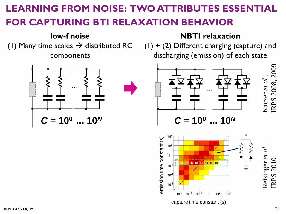
LEARNING FROM NOISE: TWO ATTRIBUTES ESSENTIAL FOR CAPTURING BTI RELAXATION BEHAVIOR
C = 100 ... 10N C = 100 ... 10N
low-f noise (1) Many time scales distributed RC
components
NBTI relaxation (1) + (2) Different charging (capture) and
discharging (emission) of each state
Kac
zer e
t al.,
IR
PS 2
008,
200
9
capture time constant (s)
emis
sion
tim
e co
nsta
nt (s
)
Rei
sing
er e
t al.,
IR
PS 2
010
BEN KACZER, IMEC 72 BEN KACZER, IMEC
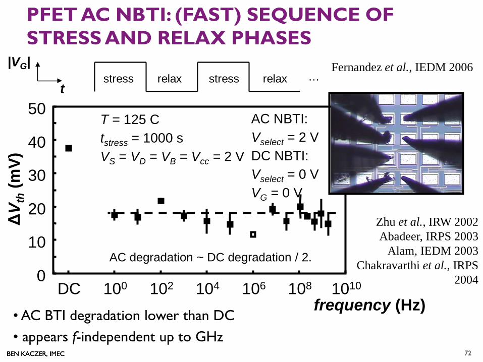
PFET AC NBTI: (FAST) SEQUENCE OF STRESS AND RELAX PHASES
0
10
20
30
40
50
100 102 104 106 108 1010
frequency (Hz)
ΔV t
h (m
V)
DC
T = 125 C tstress = 1000 s VS = VD = VB = Vcc = 2 V
AC NBTI: Vselect = 2 V DC NBTI: Vselect = 0 V VG = 0 V
AC degradation ~ DC degradation / 2.
• AC BTI degradation lower than DC • appears f-independent up to GHz
72
|VG|
tstress relax stress relax …
Zhu et al., IRW 2002 Abadeer, IRPS 2003
Alam, IEDM 2003 Chakravarthi et al., IRPS
2004
Fernandez et al., IEDM 2006
BEN KACZER, IMEC BEN KACZER, IMEC
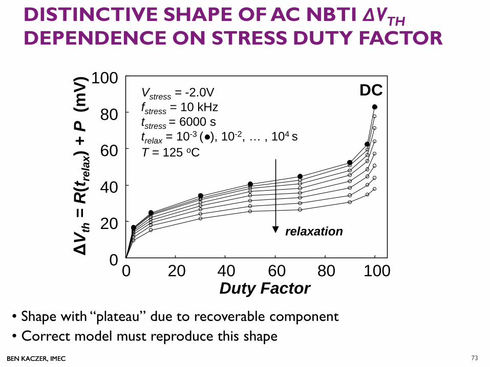
0
20
40
60
80
100
0 20 40 60 80 100 Duty Factor
ΔV t
h = R
(t rel
ax) +
P (
mV)
Vstress = -2.0V fstress = 10 kHz tstress = 6000 s trelax = 10-3 ( ), 10-2, … , 104
s T = 125 oC
relaxation
DISTINCTIVE SHAPE OF AC NBTI ΔVTH DEPENDENCE ON STRESS DUTY FACTOR
• Shape with “plateau” due to recoverable component • Correct model must reproduce this shape
DC
73
BEN KACZER, IMEC BEN KACZER, IMEC
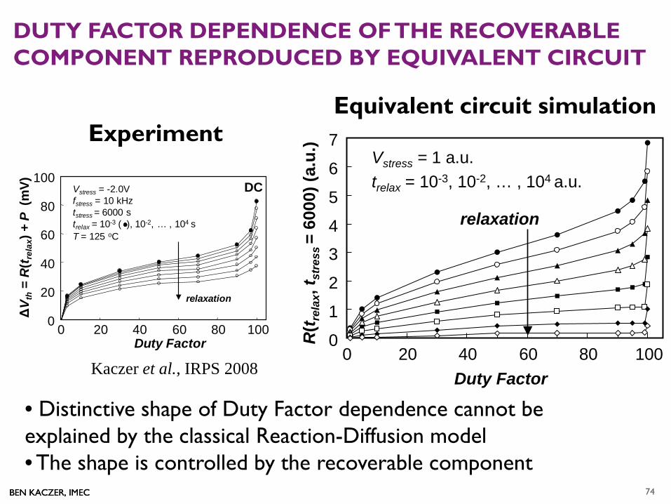
DUTY FACTOR DEPENDENCE OF THE RECOVERABLE COMPONENT REPRODUCED BY EQUIVALENT CIRCUIT
74
Kaczer et al., IRPS 2008
0 1 2 3 4 5 6 7
0 20 40 60 80 100 Duty Factor
R(t r
elax
, tst
ress
= 6
000)
(a.u
.)
Vstress = 1 a.u. trelax = 10-3, 10-2, … , 104
a.u.
relaxation
Experiment Equivalent circuit simulation
• Distinctive shape of Duty Factor dependence cannot be explained by the classical Reaction-Diffusion model • The shape is controlled by the recoverable component
0
20
40
60
80
100
0 20 40 60 80 100Duty Factor
ΔV t
h=
R(t r
elax
) + P
(m
V) Vstress = -2.0Vfstress = 10 kHztstress = 6000 strelax = 10-3 ( ), 10-2, … , 104 sT = 125 oC
relaxation
DC
BEN KACZER, IMEC BEN KACZER, IMEC
OUTLINE CMOS FEOL trends
Why reliability
Examples of FET degradation mechanisms
TDDB
BTI • Overview / BTI components
• Technological remedies
• NBTI recoverable component and AC stress
• BTI in deeply scaled devices
• Observing properties of individual defects
• Impact of individual defects on FET characteristics
• Constructing and projecting ∆Vth distributions
• Combining time-dependent and time-0 variabilities
• Defect-centric circuit simulation framework
76
BEN KACZER, IMEC
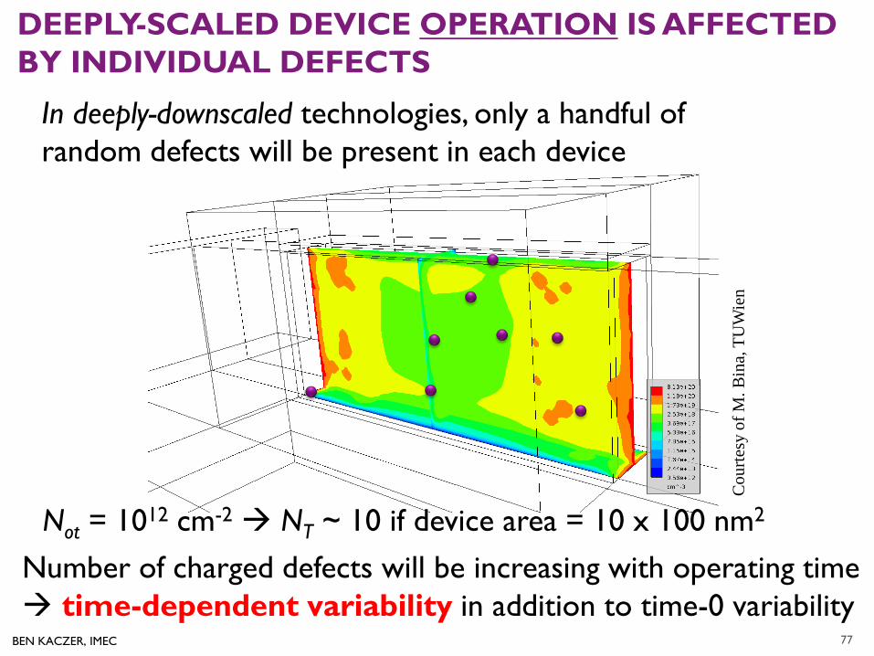
DEEPLY-SCALED DEVICE OPERATION IS AFFECTED BY INDIVIDUAL DEFECTS
77
In deeply-downscaled technologies, only a handful of random defects will be present in each device
Not = 1012 cm-2 NT ~ 10 if device area = 10 x 100 nm2
Cou
rtesy
of M
. Bin
a, T
UW
ien
Number of charged defects will be increasing with operating time time-dependent variability in addition to time-0 variability
BEN KACZER, IMEC BEN KACZER, IMEC
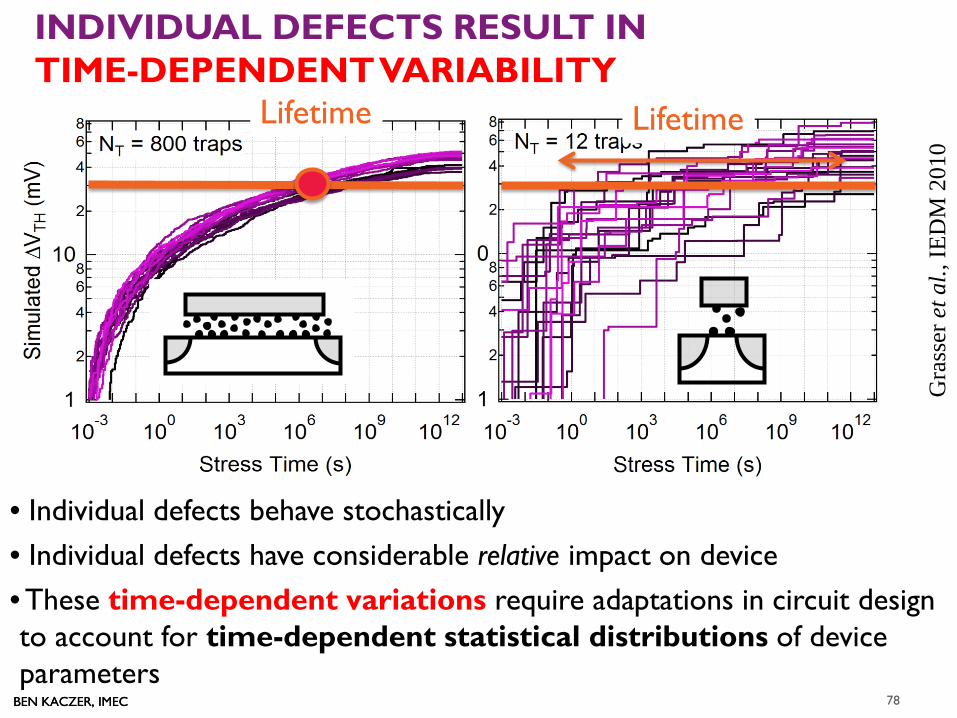
INDIVIDUAL DEFECTS RESULT IN TIME-DEPENDENT VARIABILITY
78
• Individual defects behave stochastically • Individual defects have considerable relative impact on device • These time-dependent variations require adaptations in circuit design to account for time-dependent statistical distributions of device parameters
Large devices
Large Transistor 280 x 720 nm2
NT = 800 traps
Lifetime
Gra
sser
et a
l., IE
DM
201
0
(c)
lifetime (s)
Occ
urre
nce
Lifetime
Small device 35 x 90 nm2
NT = 12 traps
Lifetime
BEN KACZER, IMEC
DEEPLY SCALED DEVICES: INDIVIDUAL EMISSION EVENTS VISIBLE IN NBTI RELAXATION TRACES
relaxation time
-ΔV
th (m
V)
10-3 10-1 101 103 105
Large pFET
[Asenov] 0
10
20
30
40
50
60
relaxation time (s)
-ΔV
th (m
V)
10-3 10-1 101
70 × 90 nm2 pFET …
τn-1 τ1 τ2 τn-2 τn Kac
zer e
t al.,
IRPS
200
9
79
BEN KACZER, IMEC
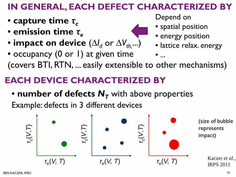
IN GENERAL, EACH DEFECT CHARACTERIZED BY • capture time τc • emission time τe • impact on device (∆Id or ∆Vth,...) • occupancy (0 or 1) at given time (covers BTI, RTN, ... easily extensible to other mechanisms)
(size of bubble represents impact)
80
Example: defects in 3 different devices
τe(V, T)
τ c(V
,T)
τe(V, T)
τ c(V
,T)
τe(V, T)
τ c(V
,T)
EACH DEVICE CHARACTERIZED BY • number of defects NT with above properties
Depend on • spatial position • energy position • lattice relax. energy • ...
Kaczer et al., IRPS 2011
BEN KACZER, IMEC
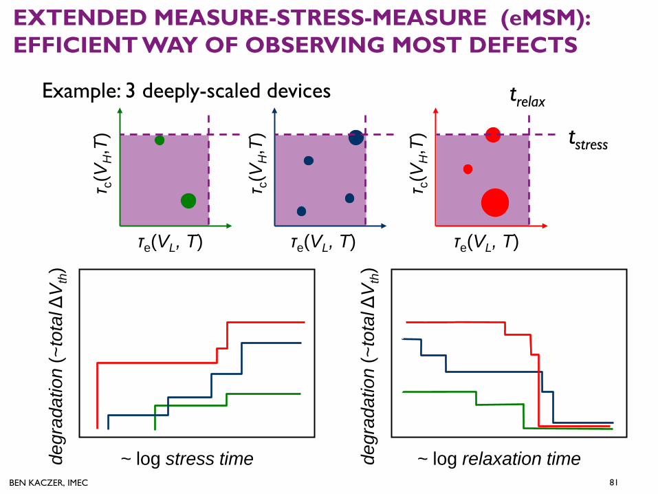
EXTENDED MEASURE-STRESS-MEASURE (eMSM): EFFICIENT WAY OF OBSERVING MOST DEFECTS
~ log stress time degr
adat
ion
(~to
tal Δ
Vth
)
Example: 3 deeply-scaled devices
81
~ log relaxation time degr
adat
ion
(~to
tal Δ
Vth
)
τe(VL, T)
τ c(V
H,T
)
τe(VL, T) τ c
(VH,T
) τe(VL, T)
τ c(V
H,T
) tstress
trelax
BEN KACZER, IMEC
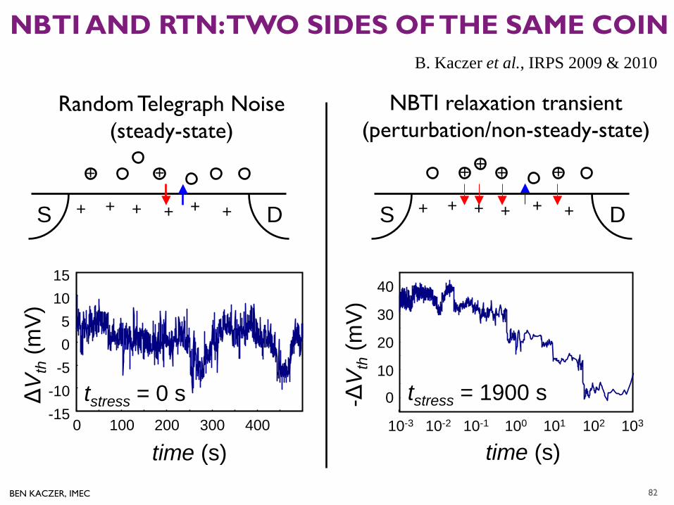
NBTI AND RTN: TWO SIDES OF THE SAME COIN
82
Random Telegraph Noise (steady-state)
NBTI relaxation transient (perturbation/non-steady-state)
S D + + + + + +
+ + + +
0
10
20
30
40
10-3 10-2 10-1 100
-ΔV
th (m
V)
time (s)
tstress = 1900 s 101 102 103
+ + + + + +
+ +
S D
-15 -10 -5 0 5
10 15
0 100 200 300 400
time (s)
tstress = 0 s ΔV
th (m
V)
B. Kaczer et al., IRPS 2009 & 2010
BEN KACZER, IMEC
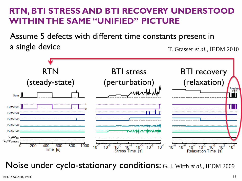
RTN, BTI STRESS AND BTI RECOVERY UNDERSTOOD WITHIN THE SAME “UNIFIED” PICTURE
T. Grasser et al., IEDM 2010
Assume 5 defects with different time constants present in a single device
VG=VTH VG=VSTRESS
RTN (steady-state)
BTI stress (perturbation)
BTI recovery (relaxation)
Noise under cyclo-stationary conditions: G. I. Wirth et al., IEDM 2009 83
BEN KACZER, IMEC BEN KACZER, IMEC
OUTLINE CMOS FEOL trends
Why reliability
Examples of FET degradation mechanisms
TDDB
BTI • Overview / BTI components
• Technological remedies
• NBTI recoverable component and AC stress
• BTI in deeply scaled devices
• Observing properties of individual defects
• Impact of individual defects on FET characteristics
• Constructing and projecting ∆Vth distributions
• Combining time-dependent and time-0 variabilities
• Defect-centric circuit simulation framework
85
BEN KACZER, IMEC
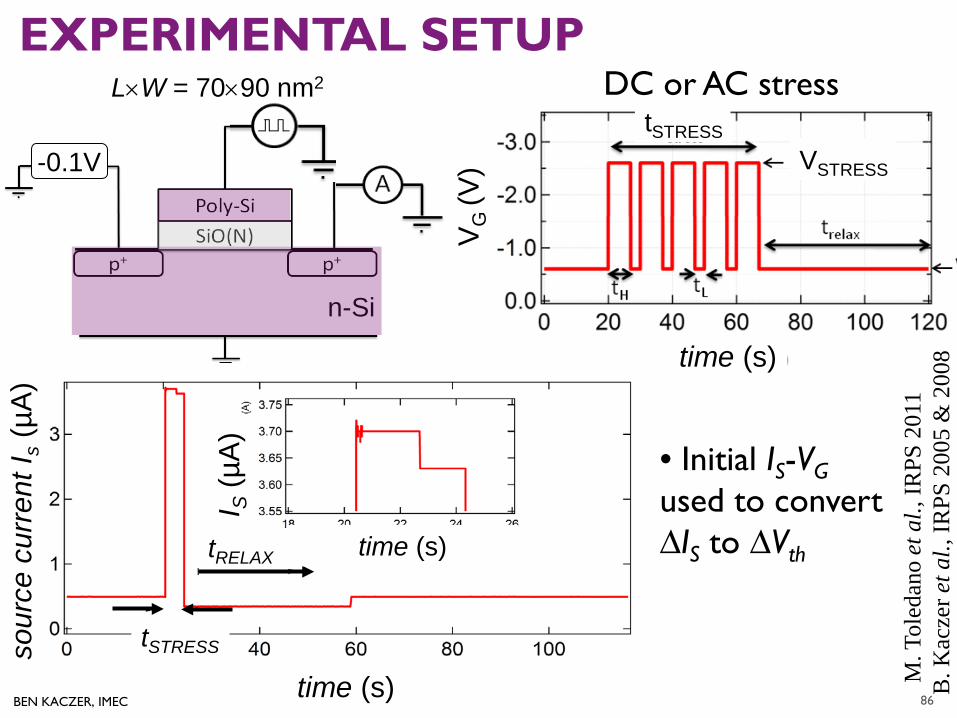
EXPERIMENTAL SETUP
-0.1V
n-Si
L×W = 70×90 nm2 tSTRESS
VSTRESS
V
G (V
)
time (s)
DC or AC stress
86 BEN KACZER time (s)
sour
ce c
urre
nt I s
(µA
)
tRELAX
tSTRESS
I S (µ
A)
time (s)
• Initial IS-VG used to convert ∆IS to ∆Vth
M. T
oled
ano
et a
l., IR
PS 2
011
B. K
acze
r et a
l., IR
PS 2
005
& 2
008
BEN KACZER, IMEC
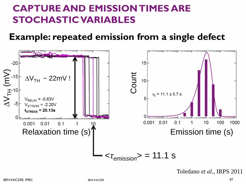
CAPTURE AND EMISSION TIMES ARE STOCHASTIC VARIABLES
∆VTH ~ 22mV !
∆VTH
(mV)
Relaxation time (s) C
ount
Emission time (s)
<τemission> = 11.1 s
Toledano et al., IRPS 2011 87
Example: repeated emission from a single defect
BEN KACZER
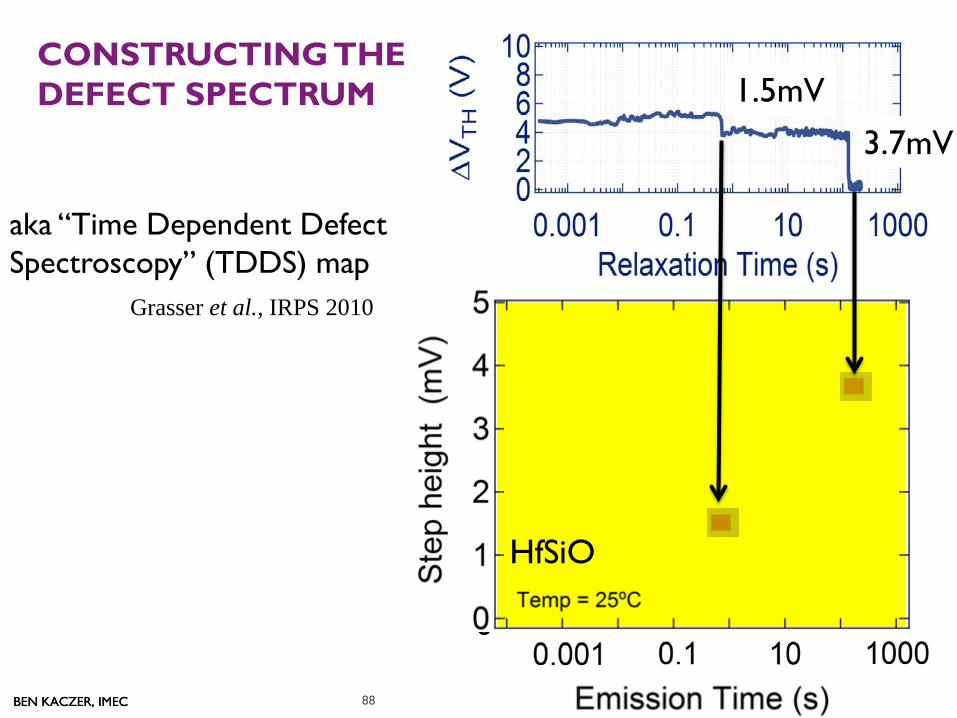
BEN KACZER, IMEC BEN KACZER, IMEC
HfSiO
3.7mV
1.5mV CONSTRUCTING THE DEFECT SPECTRUM
88
aka “Time Dependent Defect Spectroscopy” (TDDS) map
Grasser et al., IRPS 2010
BEN KACZER, IMEC BEN KACZER, IMEC
CONSTRUCTING THE DEFECT SPECTRUM 2
89
3.7mV 1.5mV
2.1mV
1.5mV
As steps reappear in multiple traces, clusters begin to form
BEN KACZER, IMEC BEN KACZER, IMEC
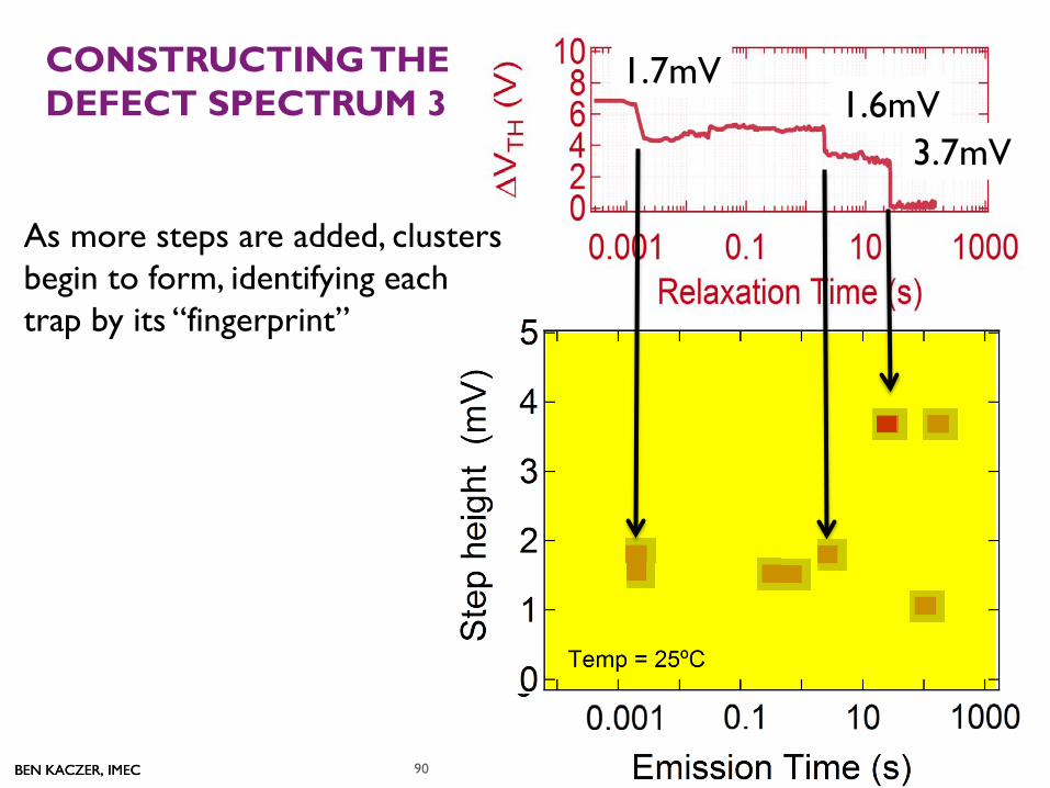
CONSTRUCTING THE DEFECT SPECTRUM 3
90
3.7mV 1.6mV
1.7mV
As more steps are added, clusters begin to form, identifying each trap by its “fingerprint”
BEN KACZER, IMEC BEN KACZER, IMEC
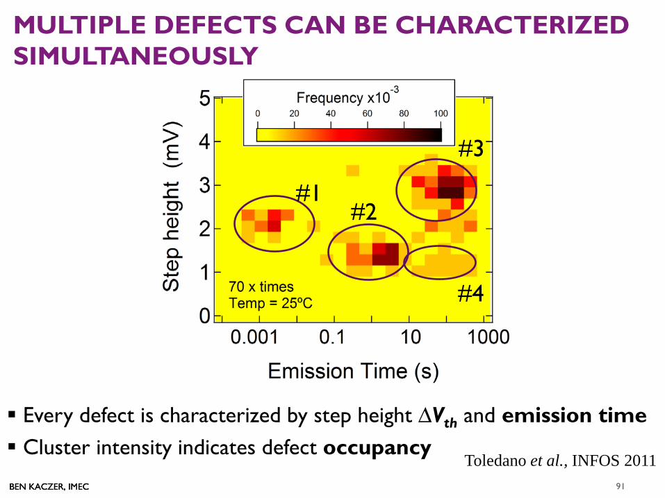
#1 #2
#3
#4
Every defect is characterized by step height ∆Vth and emission time Cluster intensity indicates defect occupancy
MULTIPLE DEFECTS CAN BE CHARACTERIZED SIMULTANEOUSLY
Toledano et al., INFOS 2011 91
BEN KACZER, IMEC
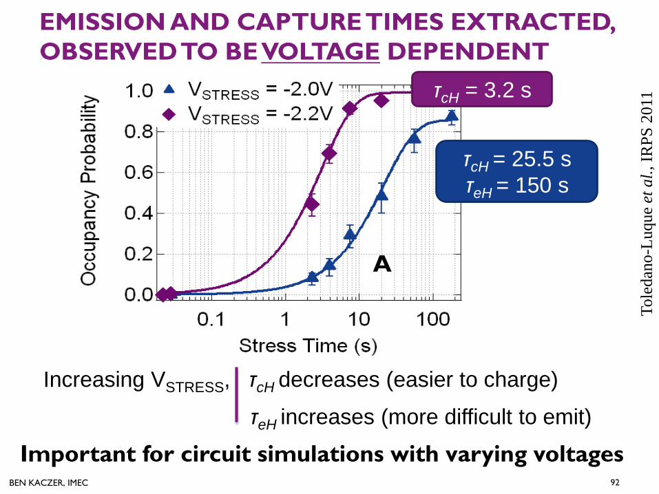
EMISSION AND CAPTURE TIMES EXTRACTED, OBSERVED TO BE VOLTAGE DEPENDENT
Increasing VSTRESS, τcH decreases (easier to charge)
τeH increases (more difficult to emit)
τcH = 3.2 s
τcH = 25.5 s τeH = 150 s
Tole
dano
-Luq
ue e
t al.,
IRPS
201
1
92
A
Important for circuit simulations with varying voltages
BEN KACZER, IMEC
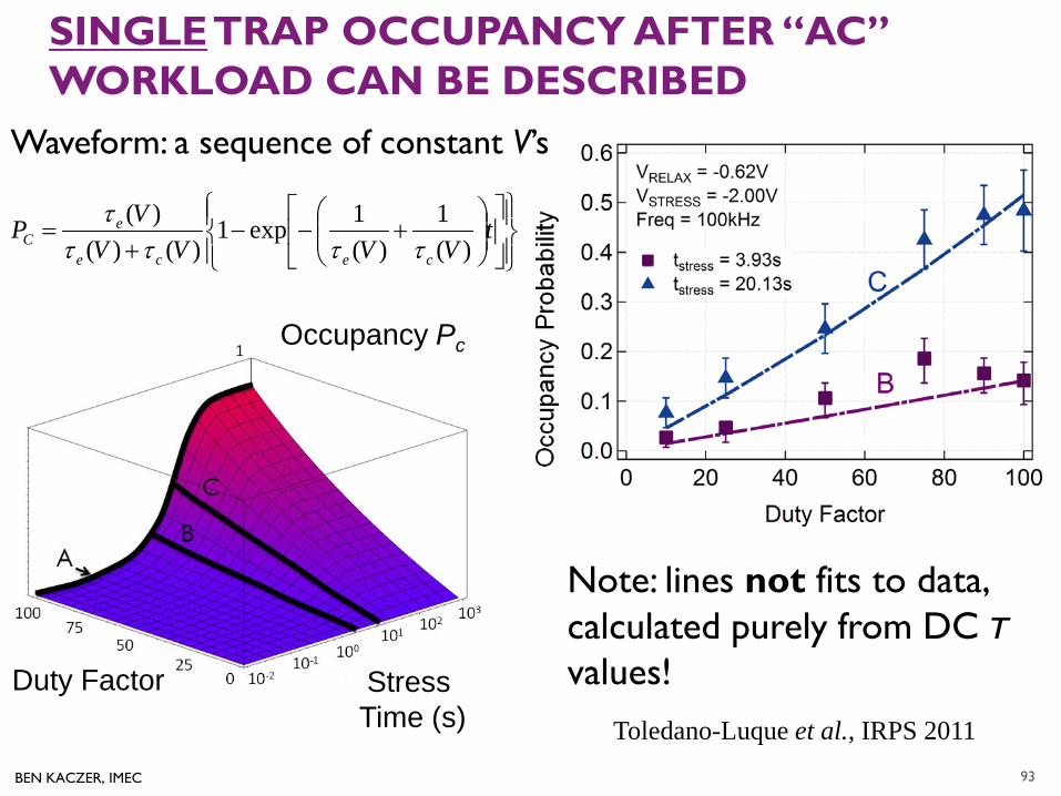
SINGLE TRAP OCCUPANCY AFTER “AC” WORKLOAD CAN BE DESCRIBED
Occupancy Pc
Stress Time (s)
Duty Factor
+−−
+= t
VVVVVP
cece
eC )(
1)(
1exp1)()(
)(ττττ
τ
Note: lines not fits to data, calculated purely from DC τ values!
Toledano-Luque et al., IRPS 2011
Waveform: a sequence of constant V’s
93
BEN KACZER, IMEC BEN KACZER, IMEC
OUTLINE CMOS FEOL trends
Why reliability
Examples of FET degradation mechanisms
TDDB
BTI • Overview / BTI components
• Technological remedies
• NBTI recoverable component and AC stress
• BTI in deeply scaled devices
• Observing properties of individual defects
• Impact of individual defects on FET characteristics
• Constructing and projecting ∆Vth distributions
• Combining time-dependent and time-0 variabilities
• Defect-centric circuit simulation framework
96
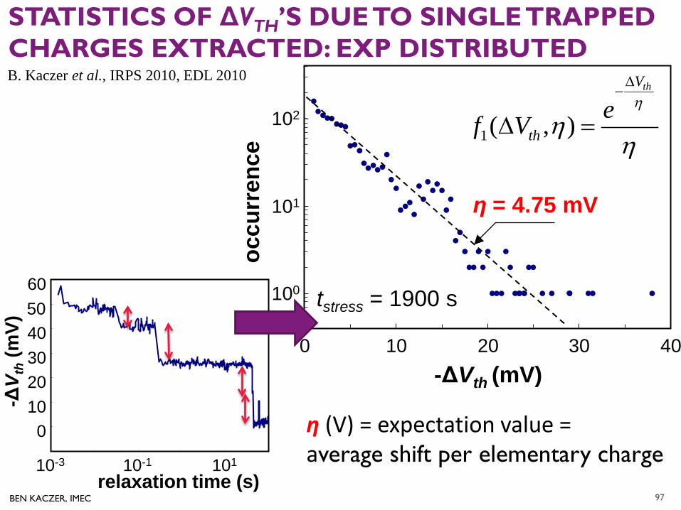
BEN KACZER, IMEC
STATISTICS OF ΔVTH’S DUE TO SINGLE TRAPPED CHARGES EXTRACTED: EXP DISTRIBUTED
97
0 10 20 30 40 50 60
relaxation time (s)
-ΔV t
h (m
V)
10-3 10-1 101
1( , )
thV
thef V
η
ηη
∆−
∆ =
100
101
102
0 10 20 30 40
occu
rren
ce
-ΔVth (mV)
tstress = 1900 s
η = 4.75 mV
η (V) = expectation value = average shift per elementary charge
B. Kaczer et al., IRPS 2010, EDL 2010
BEN KACZER, IMEC
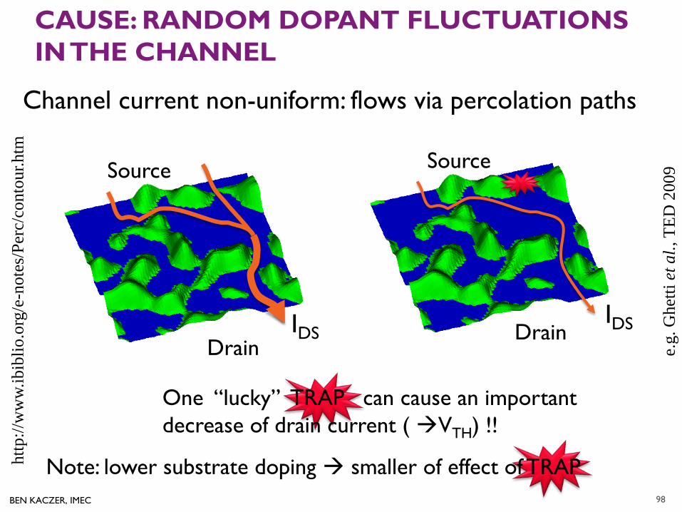
CAUSE: RANDOM DOPANT FLUCTUATIONS IN THE CHANNEL
Channel current non-uniform: flows via percolation paths
http
://w
ww.
ibib
lio.o
rg/e
-not
es/P
erc/
cont
our.h
tm
One “lucky” TRAP can cause an important decrease of drain current ( VTH) !!
Source
Drain IDS
Source
Drain IDS
e.g.
Ghe
tti e
t al.,
TED
200
9
Note: lower substrate doping smaller of effect of TRAP 98
BEN KACZER, IMEC
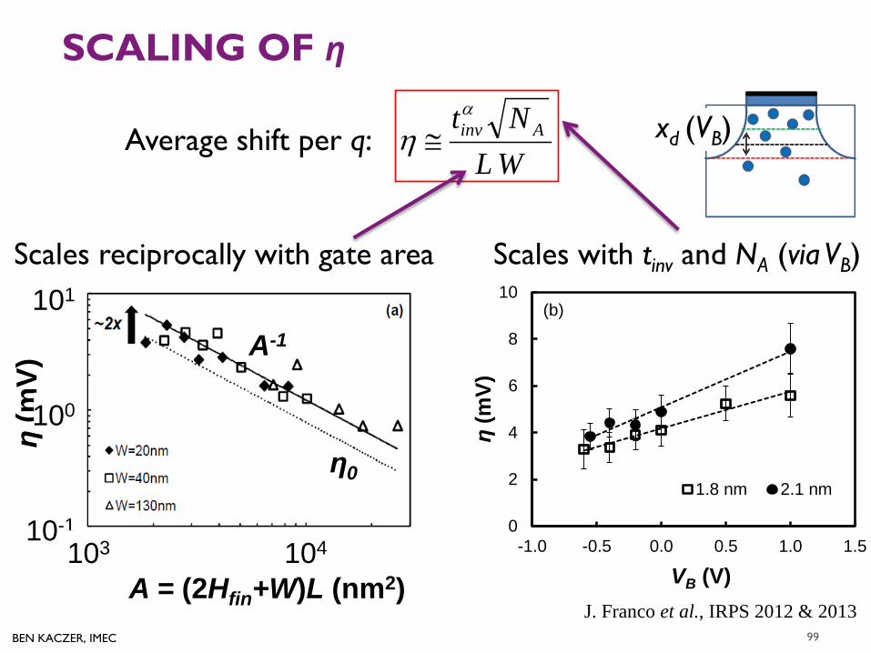
SCALING OF η
WLNt Ainv
α
η ≅Average shift per q:
0
2
4
6
8
10
-1.0 -0.5 0.0 0.5 1.0 1.5
η(m
V)
VB (V)
1.8 nm 2.1 nm
(b)
Scales with tinv and NA (via VB)
xd (VB)
η (m
V)
101
10-1
100
103 104
A = (2Hfin+W)L (nm2)
A-1
η0
Scales reciprocally with gate area
99
J. Franco et al., IRPS 2012 & 2013
BEN KACZER, IMEC
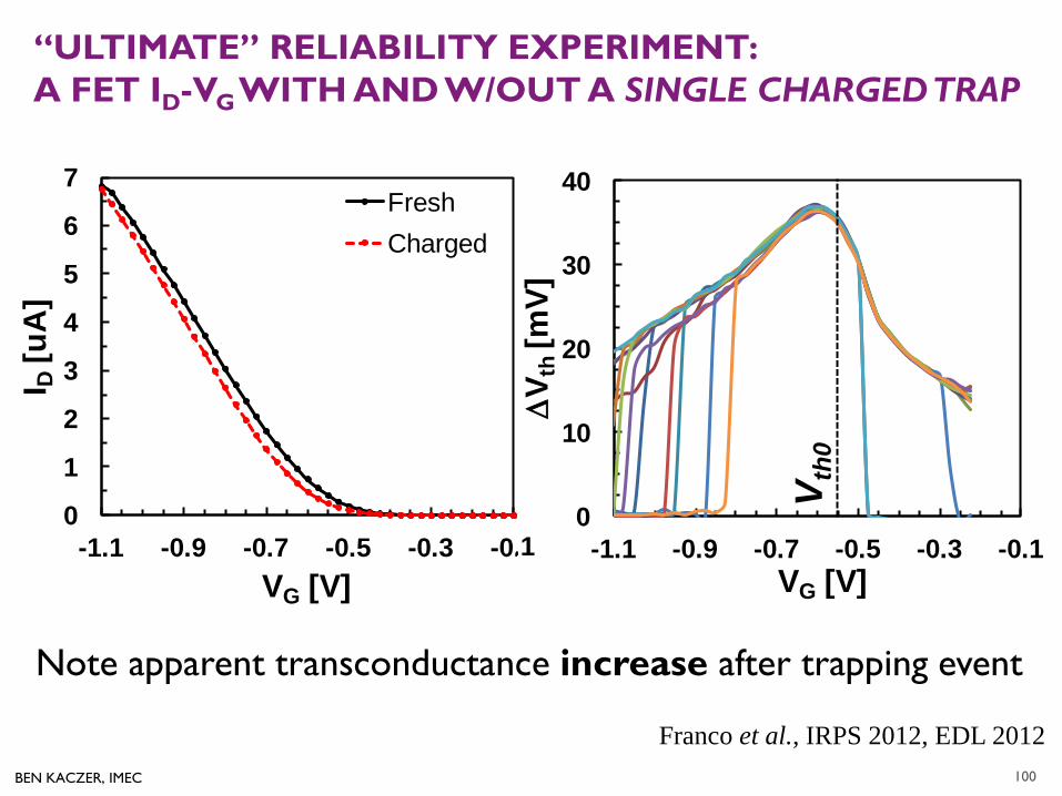
“ULTIMATE” RELIABILITY EXPERIMENT: A FET ID-VG WITH AND W/OUT A SINGLE CHARGED TRAP
100
Franco et al., IRPS 2012, EDL 2012
0
1
2
3
4
5
6
7
-1.1 -0.9 -0.7 -0.5 -0.3 -0.
I D[u
A]
VG [V]
FreshCharged
∆Vth(VG)
Note apparent transconductance increase after trapping event
.10
10
20
30
40
-1.1 -0.9 -0.7 -0.5 -0.3 -0.1∆
V th
[mV]
VG [V]
V th0
BEN KACZER, IMEC BEN KACZER, IMEC
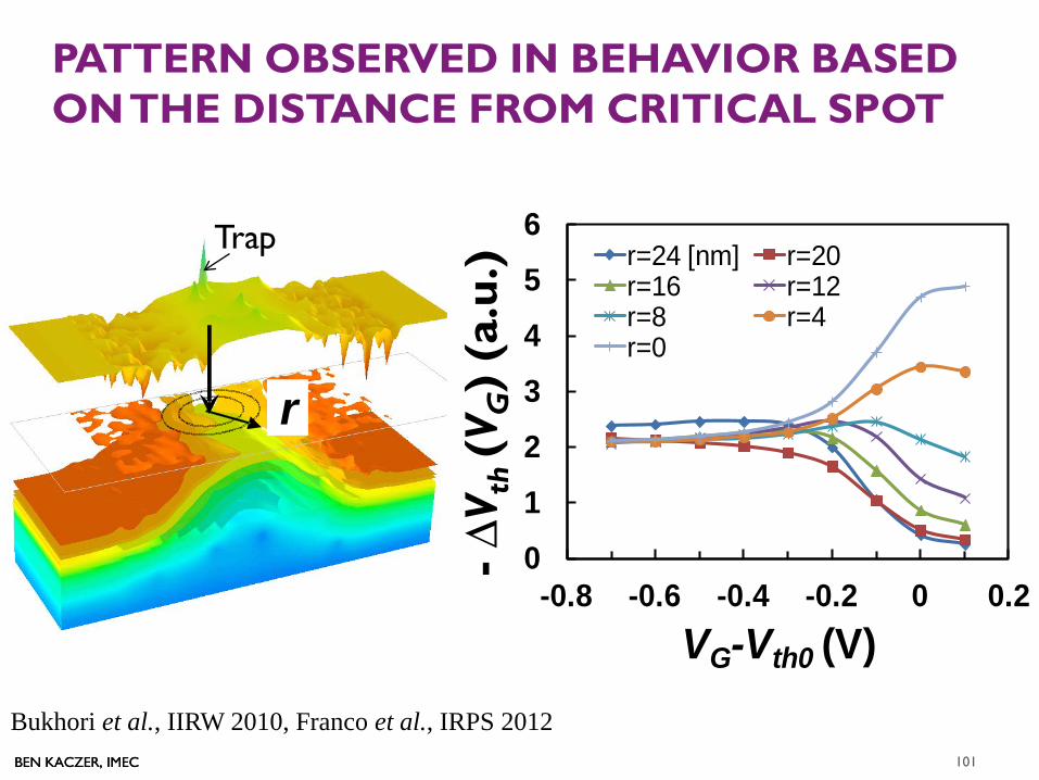
PATTERN OBSERVED IN BEHAVIOR BASED ON THE DISTANCE FROM CRITICAL SPOT
Trap
Bukhori et al., IIRW 2010, Franco et al., IRPS 2012
r
0
1
2
3
4
5
6
-0.8 -0.6 -0.4 -0.2 0 0.2-∆V t
h/∆
V th_
char
ge_s
heet
VG-Vth0 (V)
r=24 [nm] r=20r=16 r=12r=8 r=4r=0
- ∆
V th (V
G)
(a.u
.)
101
BEN KACZER, IMEC BEN KACZER, IMEC
OUTLINE CMOS FEOL trends
Why reliability
Examples of FET degradation mechanisms
TDDB
BTI • Overview / BTI components
• Technological remedies
• NBTI recoverable component and AC stress
• BTI in deeply scaled devices
• Observing properties of individual defects
• Impact of individual defects on FET characteristics
• Constructing and projecting ∆Vth distributions
• Combining time-dependent and time-0 variabilities
• Defect-centric circuit simulation framework
102

BEN KACZER, IMEC
PARADIGM SHIFT IN RELIABILITY PREDICTIONS
Instead of averages, lifetime distributions projected
103
~ log stress time degr
adat
ion
(~to
tal Δ
Vth
)
Past (large devices)
~ log stress time degr
adat
ion
(~to
tal Δ
Vth
)
Present (small devices)
“Classical” reliability Time-Dependent Variability

BEN KACZER, IMEC
CONSTRUCTING TOTAL DEVICE-TO-DEVICE ΔVTH DISTRIBUTION
1) Exponential distribution of ΔVth steps due to a single defect
100
101
102
0 10 20 30 40
occu
rren
ce
-ΔVth (mV)
tstress = 1900 s
η = 4.75 mV
η
ηthV
theVf
∆−
=∆ )(
104
D
S
D
S
D
S
D
S
D
S
…
Kac
zer e
t al.,
ED
L 20
10 2) Poisson distribution of the average number of defects NT
(note: NT = W L Not)
BEN KACZER, IMEC BEN KACZER, IMEC
-3
-2
-1
0
1
2
3
4
0 40 80 120 160-ΔVth (mV)
0.010.1131030507090979999.999.99
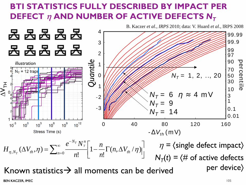
BTI STATISTICS FULLY DESCRIBED BY IMPACT PER DEFECT η AND NUMBER OF ACTIVE DEFECTS NT
∆Γ−=∆ ∑∞
=
−
)/,(!
1!
),(0, ηηη thn
nN
thN Vnnn
nNe
VH TT
T
ΔVT
H
η = ⟨single defect impact⟩ NT(t) = ⟨# of active defects
per device⟩
-3
-2
-1
0
1
2
3
4
0 40 80 120 160
prob
it(F
N)
-ΔVth (mV)
0.010.1131030507090979999.999.99
percentile
NT = 1, 2, .., 20
η ≈ 4 mVNT = 6NT = 9NT = 14
B. Kaczer et al., IRPS 2010; data: V. Huard et al., IRPS 2008
Q
uant
ile
Known statistics all moments can be derived
illustration
105
BEN KACZER, IMEC BEN KACZER, IMEC
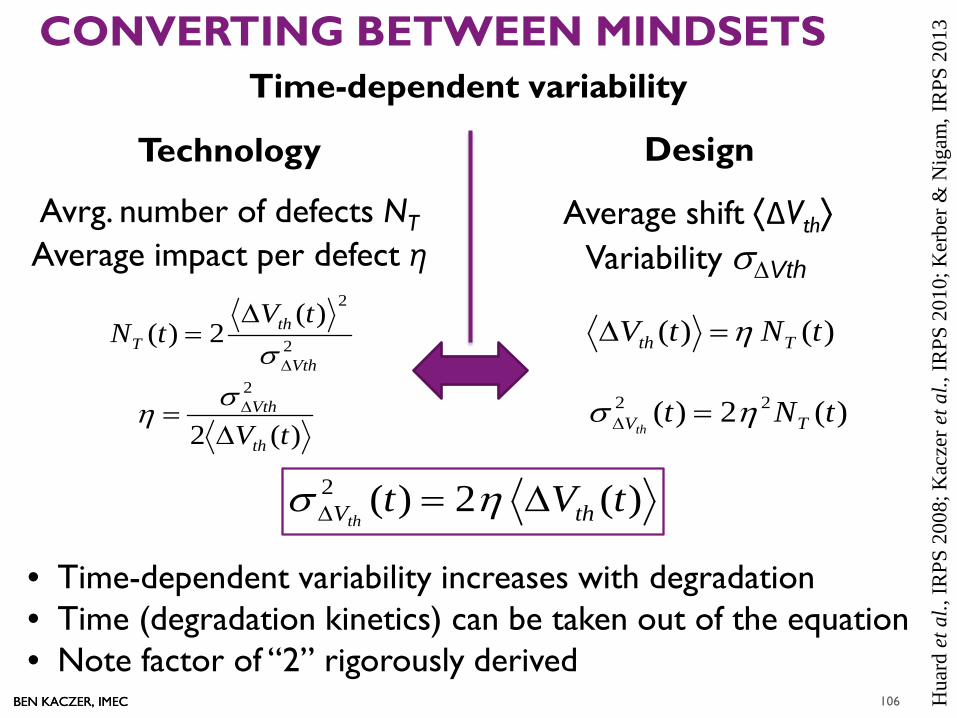
CONVERTING BETWEEN MINDSETS
Design
Average shift ⟨ΔVth⟩ Variability σ∆Vth
)(2)(2 tVt thVth∆=∆ ησ
)()( tNtV Tth η=∆2
2)(2)(
Vth
thT
tVtN
∆
∆=
σ
)(2
2
tVth
Vth
∆= ∆ση )(2)( 22 tNt TVth
ησ =∆
• Time-dependent variability increases with degradation • Time (degradation kinetics) can be taken out of the equation • Note factor of “2” rigorously derived
Hua
rd e
t al.,
IRPS
200
8; K
acze
r et a
l., IR
PS 2
010;
Ker
ber &
Nig
am, I
RPS
201
3
Technology
Avrg. number of defects NT
Average impact per defect η
Time-dependent variability
106
BEN KACZER, IMEC
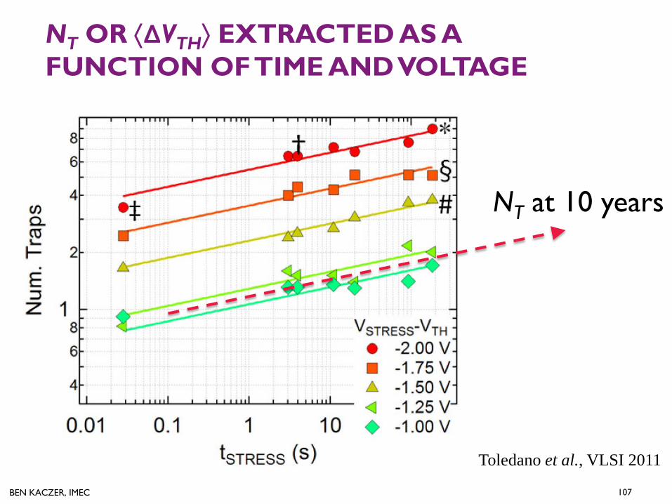
NT OR ⟨ΔVTH⟩ EXTRACTED AS A FUNCTION OF TIME AND VOLTAGE
NT at 10 years
Toledano et al., VLSI 2011
107
BEN KACZER, IMEC
A FRACTION OF DEEPLY-SCALED DEVICES EXCEEDS FAILURE CRITERIA AT LOWER OVERDRIVES
M. T
oled
ano
et a
l., V
LSI 2
011
median
108
BEN KACZER, IMEC BEN KACZER, IMEC
OUTLINE CMOS FEOL trends
Why reliability
Examples of FET degradation mechanisms
TDDB
BTI • Overview / BTI components
• Technological remedies
• NBTI recoverable component and AC stress
• Defect properties
• Observing properties of individual defects
• Impact of individual defects on FET characteristics
• Constructing and projecting ∆Vth distributions
• Combining time-dependent and time-0 variabilities
• Defect-centric circuit simulation framework
109
BEN KACZER, IMEC BEN KACZER, IMEC
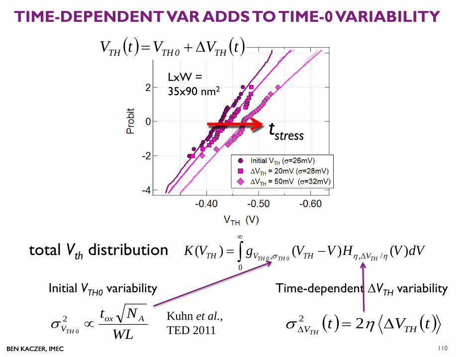
TIME-DEPENDENT VAR ADDS TO TIME-0 VARIABILITY
WLNt Aox
VTH∝2
0σ
Initial VTH0 variability Time-dependent ∆VTH variability
( ) ( )tVt THVTH∆=∆ ησ 22
Stress Time
∫∞
∆−=0
/,, )()()(00
dVVHVVgVKTHTHTH VTHVTH ηησ
( ) ( )tVVtV TH0THTH ∆+=
total Vth distribution
Kuhn et al., TED 2011
LxW = 35x90 nm2
tstress
110
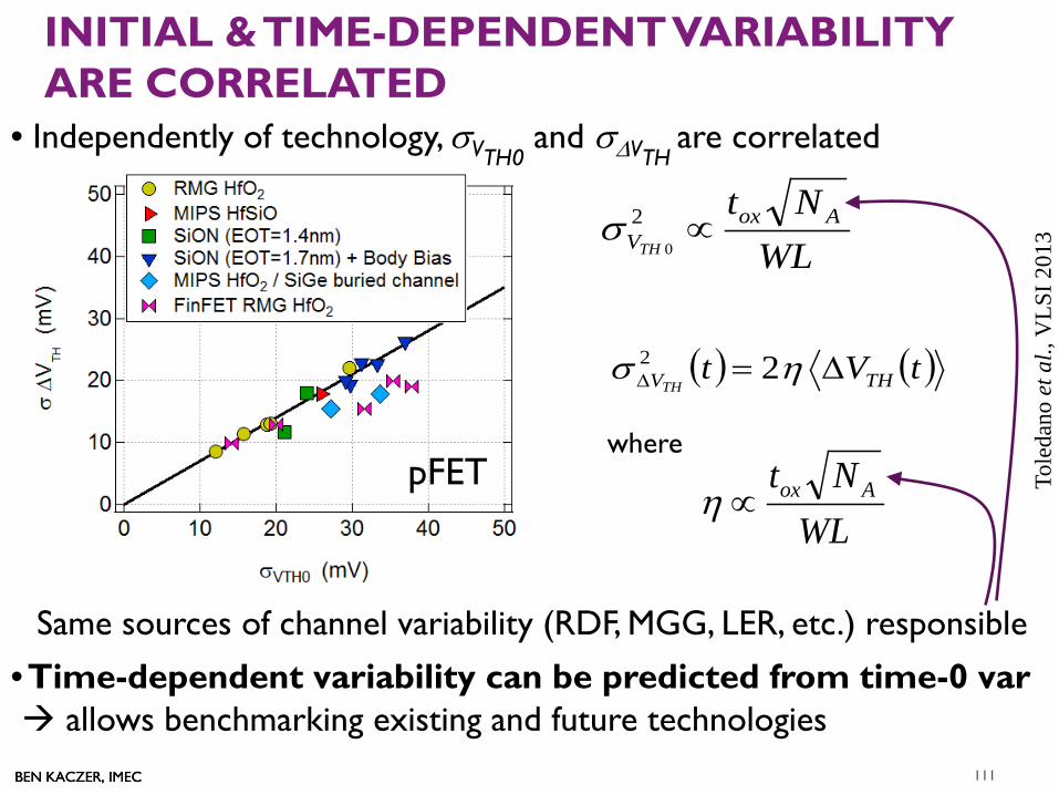
BEN KACZER, IMEC BEN KACZER, IMEC
• Independently of technology, σVTH0 and σ∆VTH are correlated
INITIAL & TIME-DEPENDENT VARIABILITY ARE CORRELATED
WLNt Aox
VTH∝2
0σ
( ) ( )tVt THVTH∆=∆ ησ 22
WLNt Aox∝η
where
Same sources of channel variability (RDF, MGG, LER, etc.) responsible
Tole
dano
et a
l., V
LSI 2
013
• Time-dependent variability can be predicted from time-0 var allows benchmarking existing and future technologies
111
pFET
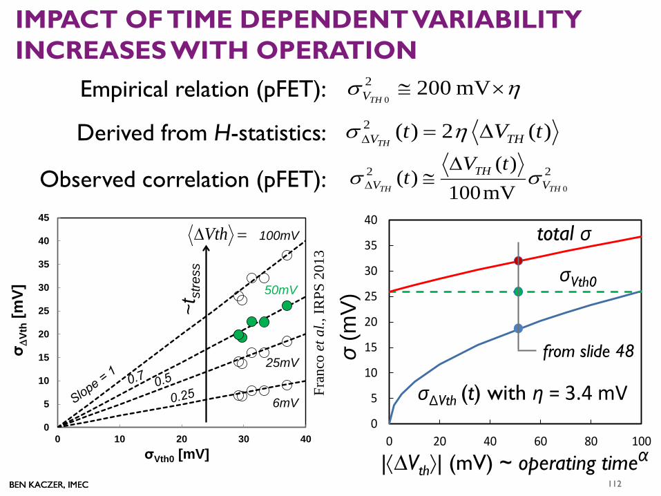
BEN KACZER, IMEC BEN KACZER, IMEC
0
5
10
15
20
25
30
35
40
0 20 40 60 80 100
from slide 48
IMPACT OF TIME DEPENDENT VARIABILITY INCREASES WITH OPERATION
total σ
0
5
10
15
20
25
30
35
40
45
0 10 20 30 40
σ ∆Vt
h[m
V]
σVth0 [mV]
=∆Vth 100mV
50mV
25mV
6mV
~tst
ress
|⟨∆Vth⟩| (mV) ~ operating timeα
σ (m
V) σVth0
σ∆Vth (t) with η = 3.4 mV
)(2)(2 tVt THVTH∆=∆ ησ
Fran
co e
t al.,
IRPS
201
3
ησ ×≅ mV20020THVEmpirical relation (pFET):
Derived from H-statistics: 22
0mV100)(
)(THTH V
THV
tVt σσ
∆≅∆Observed correlation (pFET):
112
BEN KACZER, IMEC BEN KACZER, IMEC
OUTLINE CMOS FEOL trends
Why reliability
Examples of FET degradation mechanisms
TDDB
BTI • Overview / BTI components
• Technological remedies
• NBTI recoverable component and AC stress
• BTI in deeply scaled devices
• Observing properties of individual defects
• Impact of individual defects on FET characteristics
• Constructing and projecting ∆Vth distributions
• Combining time-dependent and time-0 variabilities
• Defect-centric circuit simulation framework
114
BEN KACZER, IMEC
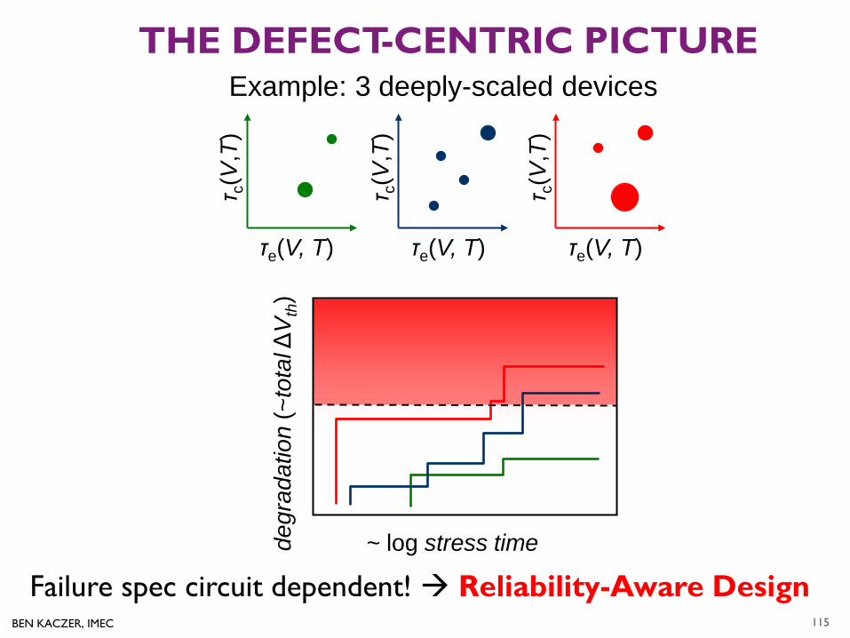
THE DEFECT-CENTRIC PICTURE
115
~ log stress time degr
adat
ion
(~to
tal Δ
Vth
)
τe(V, T) τ c
(V,T
) τe(V, T)
τ c(V
,T)
τe(V, T)
τ c(V
,T)
Example: 3 deeply-scaled devices
Failure spec circuit dependent! Reliability-Aware Design
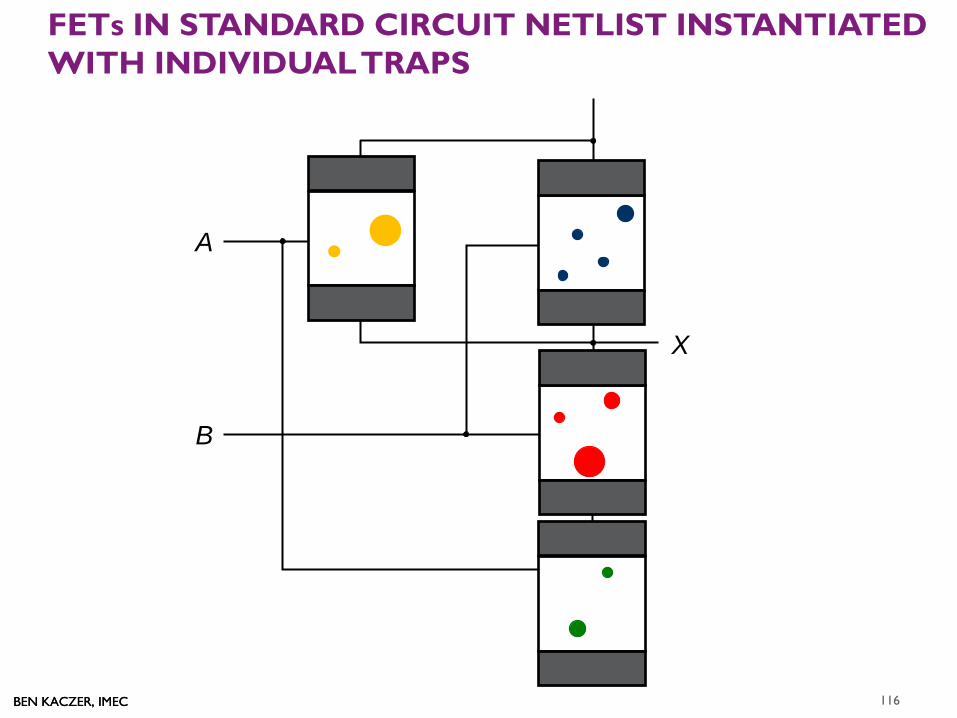
BEN KACZER, IMEC BEN KACZER, IMEC
FETs IN STANDARD CIRCUIT NETLIST INSTANTIATED WITH INDIVIDUAL TRAPS
A
B
X
116
BEN KACZER, IMEC BEN KACZER, IMEC
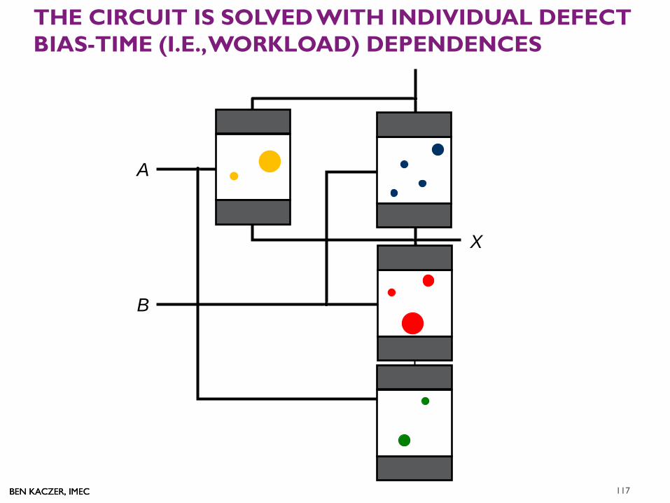
THE CIRCUIT IS SOLVED WITH INDIVIDUAL DEFECT BIAS-TIME (I.E., WORKLOAD) DEPENDENCES
A
B
X
117
BEN KACZER, IMEC
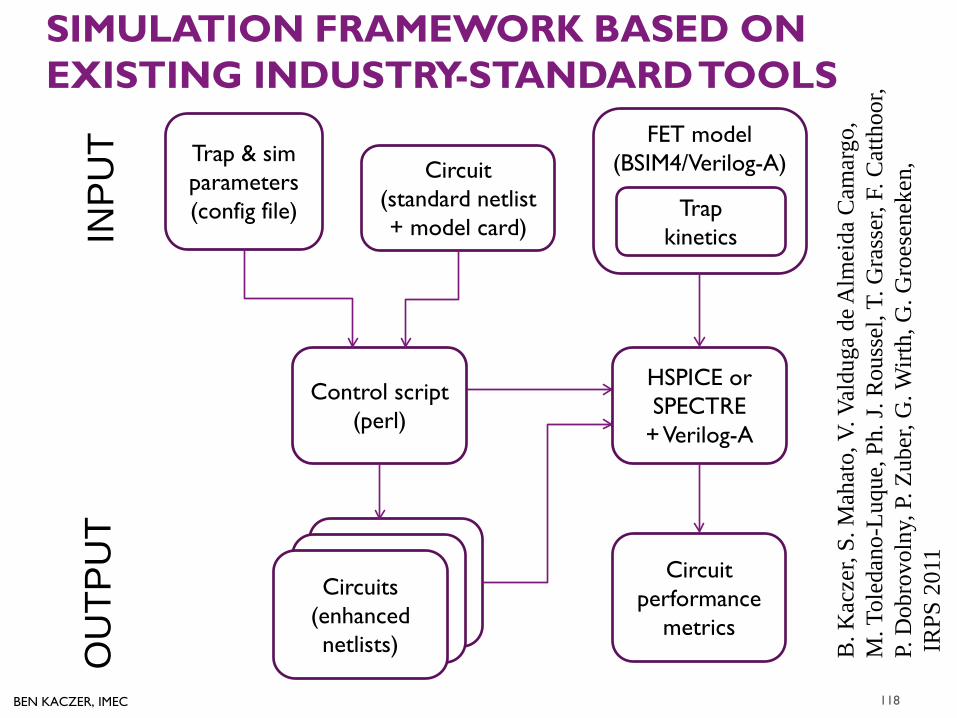
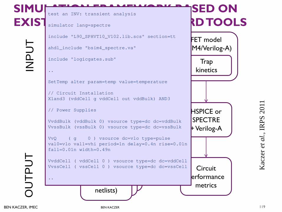
SIMULATION FRAMEWORK BASED ON EXISTING INDUSTRY-STANDARD TOOLS
B. K
acze
r, S.
Mah
ato,
V. V
aldu
ga d
e Alm
eida
Cam
argo
,
M
. Tol
edan
o-Lu
que,
Ph.
J. R
ouss
el, T
. Gra
sser
, F. C
atth
oor,
P.
Dob
rovo
lny,
P. Z
uber
, G. W
irth,
G. G
roes
enek
en,
IRPS
201
1
Circuit (standard netlist + model card)
FET model (BSIM4/Verilog-A)
Control script (perl)
Trap & sim parameters (config file)
HSPICE or SPECTRE
+ Verilog-A
INPU
T O
UTP
UT
Circuits (enhanced netlists)
Circuit performance
metrics
Trap kinetics
118
BEN KACZER, IMEC
SIMULATION FRAMEWORK BASED ON EXISTING INDUSTRY-STANDARD TOOLS
Kac
zer e
t al.,
IRPS
201
1
Circuit (standard netlist + model card)
FET model (BSIM4/Verilog-A)
Control script (perl)
Trap & sim parameters (config file)
HSPICE or SPECTRE
+ Verilog-A
INPU
T O
UTP
UT
Circuits (enhanced netlists)
Circuit performance
metrics
Trap kinetics
test an INV: transient analysis simulator lang=spectre include "L90_SPHVT10_V102.lib.scs" section=tt ahdl_include "bsim4_spectre.va" include "logicgates.sub" .. SetTemp alter param=temp value=temperature // Circuit Installation X1and3 (vddCell g vddCell out vddBulk) AND3 // Power Supplies VvddBulk (vddBulk 0) vsource type=dc dc=vddBulk VvssBulk (vssBulk 0) vsource type=dc dc=vssBulk VvQ ( g 0 ) vsource dc=vlo type=pulse val0=vlo val1=vhi period=1n delay=0.4n rise=0.01n fall=0.01n width=0.49n VvddCell ( vddCell 0 ) vsource type=dc dc=vddCell VvssCell ( vssCell 0 ) vsource type=dc dc=vssCell ..
119 BEN KACZER
BEN KACZER, IMEC
SIMULATION FRAMEWORK BASED ON EXISTING INDUSTRY-STANDARD TOOLS
Kac
zer e
t al.,
IRPS
201
1
Circuit (standard netlist + model card)
FET model (BSIM4/Verilog-A)
Control script (perl)
Trap & sim parameters (config file)
HSPICE or SPECTRE
+ Verilog-A
INPU
T O
UTP
UT
Circuits (enhanced netlists)
Circuit performance
metrics
Trap kinetics
#Start the file spice_file = and3.scs USE store_inputs Monte = 1 internal_monte=1 language = spectre #transistor parameters vth0_mean_pmos = -0.25 vth0_sd_pmos = 0.05 vth0_mean_nmos = 0.25 vth0_sd_nmos = 0.05 #Traps density# pmos_trap_density_sio2 = 9e10 nmos_trap_density_sio2 = 5e10 nmos_trap_density_hk = 2e10 #standard transistor definition wp=90nm lp=70nm wn=90nm ln=70nm #input history start_time=0 ..
120
BEN KACZER, IMEC
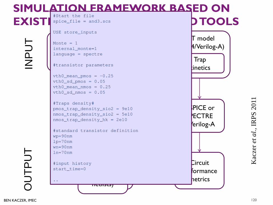
SIMULATION FRAMEWORK BASED ON EXISTING INDUSTRY-STANDARD TOOLS
Kac
zer e
t al.,
IRPS
201
1
Circuit (standard netlist + model card)
FET model (BSIM4/Verilog-A)
Control script (perl)
Trap & sim parameters (config file)
HSPICE or SPECTRE
+ Verilog-A
INPU
T O
UTP
UT
Circuits (enhanced netlists)
Circuit performance
metrics
Trap kinetics
.. Nmnmos3_X1nand_X1and3 (_X1nand_X1and3_midnode vddCell 0 0) bsim4_va type=1 l=80nm w=100nm*1*2 vth0=0.224068372498511 Ntraps=8 VH=0.8 VL=0 len=8 DeltaVth=[ 0.00021502392265272 0.00129168432396303 0.0047480549849773 0.0011596499954241 0.0018326350216282 0.00177542424038912 0.00122528625484488 0.00193559032206868 ] tcH=[ 0.0034617748767338 2.9514020629307e-11 2.35108924858284e-07 7.50085687666976e-10 1.34632779405625e-06 1.09448440801564e-12 4.64052202957496e-11 1.53225235524155e-06 ] tcL=[ 100000000 100000000 100000000 100000000 100000000 100000000 100000000 100000000 ] teH=[ 0.304046922519998 2.77299758745423e-06 1.0359818715254 0.00901532692412415 0.000905011102154941 2.86728323688865e-06 0.000135952087963774 0.018531074298117 ] teL=[ 0.00185336582376316 4.43992015382931e-08 0.0144582180307964 0.000171466248546535 4.396634106273e-07 2.76627004569314e-08 4.38821936112408e-07 0.000238047697343963 ] ic_trap=[ 0 0 0 0 0 0 0 0 ] device_seed=1301500415 ..
121
BEN KACZER, IMEC
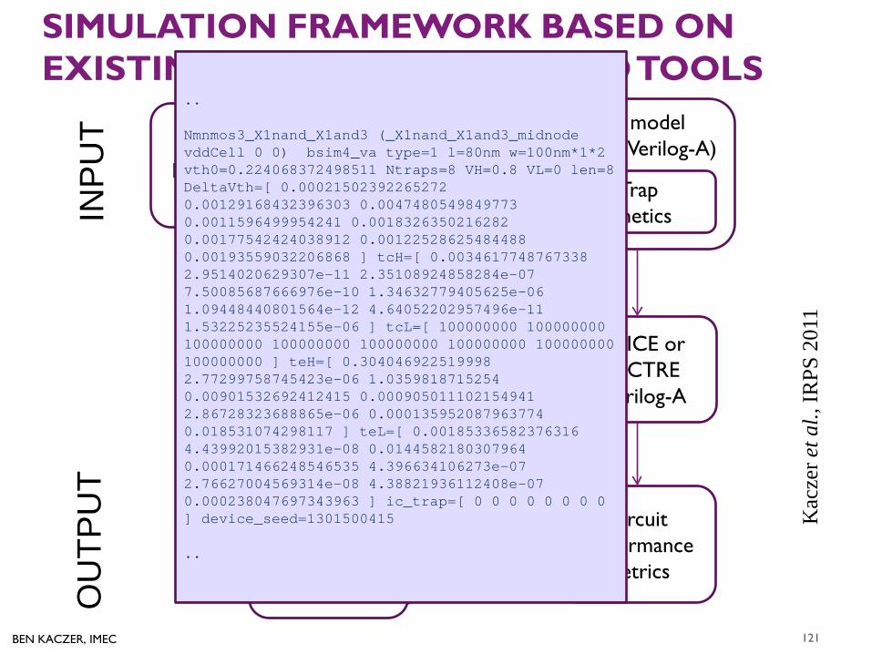
SIMULATION FRAMEWORK BASED ON EXISTING INDUSTRY-STANDARD TOOLS
Kac
zer e
t al.,
IRPS
201
1
Circuit (standard netlist + model card)
FET model (BSIM4/Verilog-A)
Control script (perl)
Trap & sim parameters (config file)
HSPICE or SPECTRE
+ Verilog-A
INPU
T O
UTP
UT
Circuits (enhanced netlists)
Circuit performance
metrics
Trap kinetics
∆
+−−
+= tP
vcvevcve
vpvp
,,,,
,,
11exp1ττττ
τ
/* File's brief description: This is the include file to simulate the defect trapping and detrapping of NBTI model & Calculate the total occupancy of defects. */ /********************************** START: Modified by Swaraj for NBTI***********************************/ Vth=Vth+IC_DeltaVthNbti; //Modified Vth due to inicial NBTI defect......Swaraj if(analysis("tran")) begin //$strobe(" \nNew TimeStep"); SimTime_new=$abstime; if(SimTime_new >= SimTime_old)begin TimeStep=SimTime_new-SimTime_old; // $strobe("Simulation Time Step=%e", TimeStep); SimTime_old=SimTime_new; end ...
122
BEN KACZER, IMEC
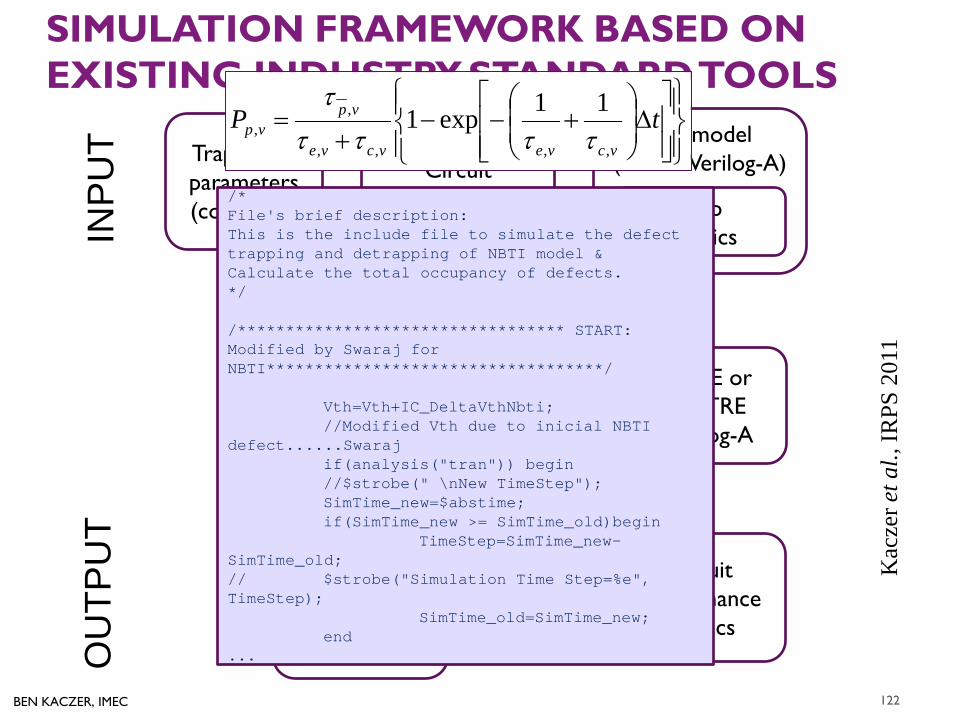
SIMULATION FRAMEWORK BASED ON EXISTING INDUSTRY-STANDARD TOOLS
Kac
zer e
t al.,
IRPS
201
1
Circuit (standard netlist + model card)
FET model (BSIM4/Verilog-A)
Control script (perl)
Trap & sim parameters (config file)
HSPICE or SPECTRE
+ Verilog-A
INPU
T O
UTP
UT
Circuits (enhanced netlists)
Circuit performance
metrics
Trap kinetics
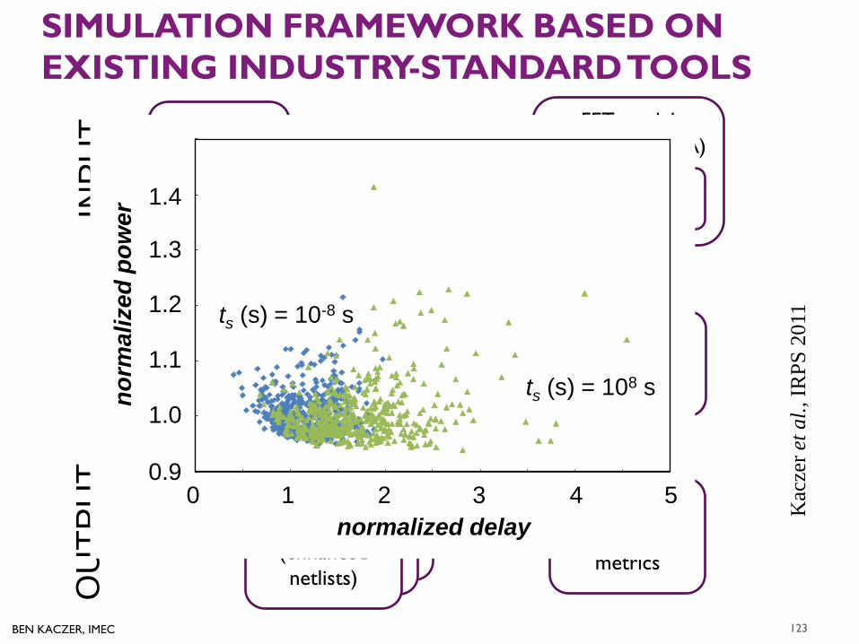
0 1 2 3 4 5 normalized delay
1.0
1.1
1.2
1.3
1.4
norm
aliz
ed p
ower
0.9
ts (s) = 10-8 s
ts (s) = 108 s
123
BEN KACZER, IMEC
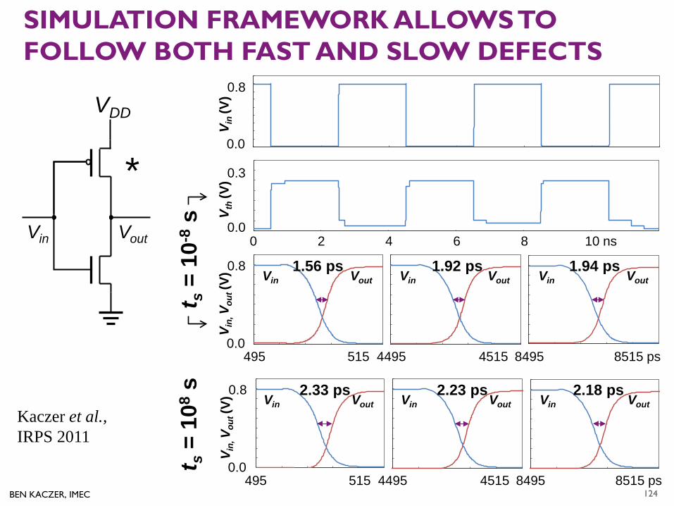
0.0
0.8
V in
(V)
0.0
0.8
V in,
Vou
t (V)
495
t s =
108
s
515 8495 4515 8515 ps 4495
Vin Vout Vin Vout Vin Vout 2.33 ps 2.23 ps 2.18 ps
SIMULATION FRAMEWORK ALLOWS TO FOLLOW BOTH FAST AND SLOW DEFECTS
VDD
* Vin Vout 0 2 4 6 8 10 ns
0.0
0.3
V th
(V)
0.0
0.8
V in,
Vou
t (V)
495 515 8495 4515 8515 ps 4495
Vin Vout Vin Vout Vin Vout 1.56 ps 1.92 ps 1.94 ps
t s =
10-
8 s
Kaczer et al., IRPS 2011
124
BEN KACZER, IMEC
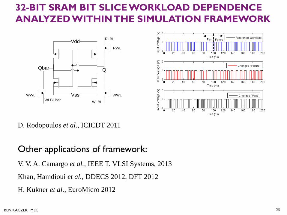
32-BIT SRAM BIT SLICE WORKLOAD DEPENDENCE ANALYZED WITHIN THE SIMULATION FRAMEWORK
Vdd
Vss
Qbar
WLBLBarWWL
WLBL
WWL
Q
RLBL
RWL
D. Rodopoulos et al., ICICDT 2011
Other applications of framework: V. V. A. Camargo et al., IEEE T. VLSI Systems, 2013
Khan, Hamdioui et al., DDECS 2012, DFT 2012
H. Kukner et al., EuroMicro 2012
125
BEN KACZER, IMEC 126
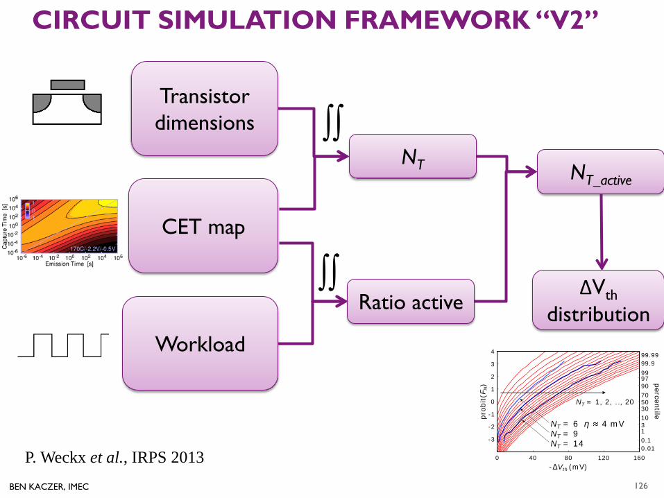
CIRCUIT SIMULATION FRAMEWORK “V2”
Transistor dimensions
CET map
Workload
NT
Ratio active
NT_active
ΔVth distribution
∫∫
∫∫
-3
-2
-1
0
1
2
3
4
0 40 80 120 160
prob
it(F
N)
-ΔVth (mV)
0.010.1131030507090979999.999.99
percentile
NT = 1, 2, .., 20
η ≈ 4 mVNT = 6NT = 9NT = 14
P. Weckx et al., IRPS 2013
BEN KACZER, IMEC 127
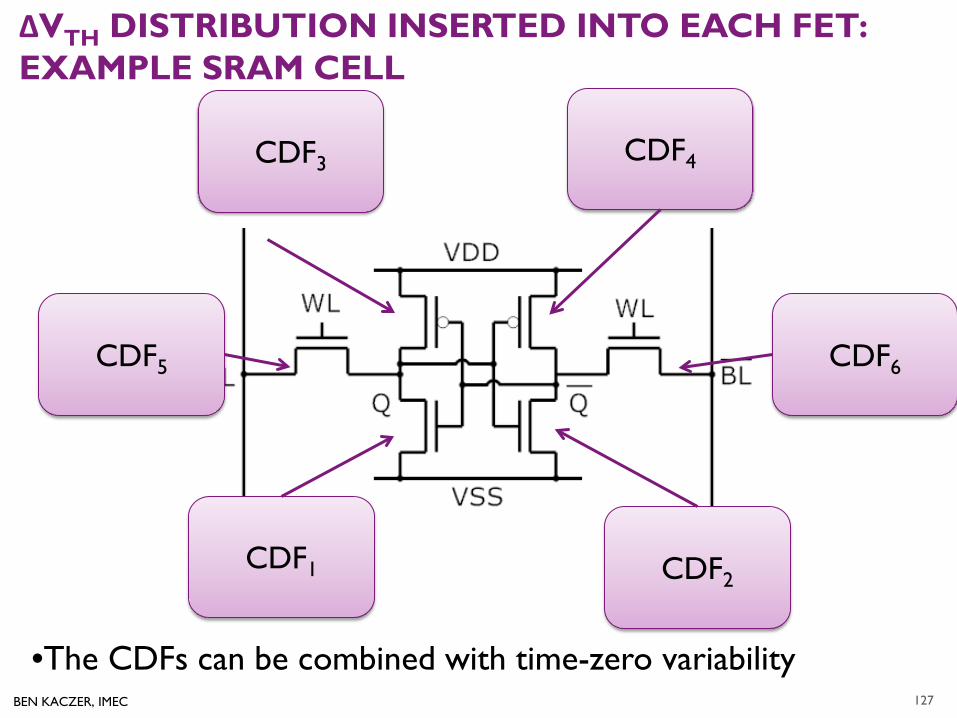
ΔVTH DISTRIBUTION INSERTED INTO EACH FET: EXAMPLE SRAM CELL
CDF4
CDF1 CDF2
CDF6 CDF5
CDF3
•The CDFs can be combined with time-zero variability
BEN KACZER, IMEC
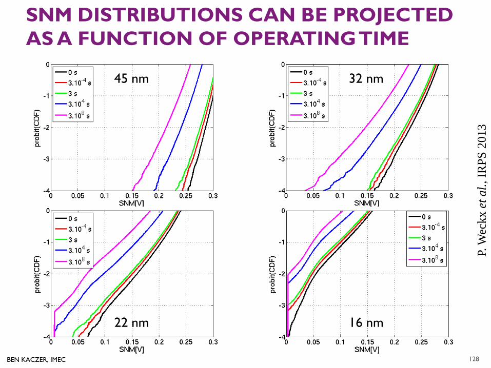
SNM DISTRIBUTIONS CAN BE PROJECTED AS A FUNCTION OF OPERATING TIME
128
45 nm 32 nm
22 nm 16 nm
P. W
eckx
et a
l., IR
PS 2
013
BEN KACZER, IMEC
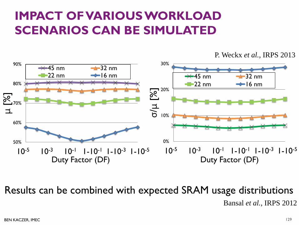
IMPACT OF VARIOUS WORKLOAD SCENARIOS CAN BE SIMULATED
129
50%
60%
70%
80%
90%
µ [%
]
45 nm 32 nm22 nm 16 nm
0%
10%
20%
30%
σ/µ
[%]
45 nm 32 nm22 nm 16 nm
10-5 10-3 10-1 1-10-1 1-10-3 1-10-5 10-5 10-3 10-1 1-10-1 1-10-3 1-10-5
Duty Factor (DF) Duty Factor (DF)
Results can be combined with expected SRAM usage distributions Bansal et al., IRPS 2012
P. Weckx et al., IRPS 2013
BEN KACZER, IMEC 130 BEN KACZER, IMEC
SUMMARY
• Reviewed the basics of • TDDB (SILC, Soft BD, progressive wear-out, Hard BD...) • and N and PBTI (Interface vs. bulk, Recoverable and
Permanent components, DC and AC stress...)
• Time-dependent (in addition to time-zero) variability will occur in future nm-sized technologies: • the “defect-centric” perspective provides basis for
understanding and mitigating reliability issues at appropriate level
130
BEN KACZER, IMEC 132 BEN KACZER, IMEC 132
THERE ARE ONLY TWO KINDS OF PEOPLE
1) Those who cannot extrapolate …