adsp-bf533 ez-kit lite evaluation system manual€¦ · adsp-bf533 ez-kit lite® evaluation system...
TRANSCRIPT
ADSP-BF533 EZ-KIT Lite®
Evaluation System Manual
Revision 1.3, April 2004
Part Number82-000730-01
Analog Devices, Inc.One Technology WayNorwood, Mass. 02062-9106 a

Copyright Information© 2004 Analog Devices, Inc., ALL RIGHTS RESERVED. This docu-ment may not be reproduced in any form without prior, express written consent from Analog Devices, Inc.
Printed in the USA.
Limited WarrantyThe EZ-KIT Lite evaluation system is warranted against defects in materi-als and workmanship for a period of one year from the date of purchase from Analog Devices or from an authorized dealer.
DisclaimerAnalog Devices, Inc. reserves the right to change this product without prior notice. Information furnished by Analog Devices is believed to be accurate and reliable. However, no responsibility is assumed by Analog Devices for its use; nor for any infringement of patents or other rights of third parties which may result from its use. No license is granted by impli-cation or otherwise under the patent rights of Analog Devices, Inc.
Trademark and Service Mark NoticeThe Analog Devices logo, VisualDSP++, VisualDSP++ logo, Blackfin, CROSSCORE logo, and EZ-KIT Lite are registered trademarks of Analog Devices, Inc.
All other brand and product names are trademarks or service marks of their respective owners.
Regulatory Compliance The ADSP-BF533 EZ-KIT Lite evaluation system has been certified to comply with the essential requirements of the European EMC directive 89/336/EEC (inclusive 93/68/EEC) and, therefore, carries the “CE” mark.
The ADSP-BF533 EZ-KIT Lite evaluation system had been appended to the Technical Construction File referenced “DSPTOOLS1” dated December 21, 1997 and was awarded CE Certification by an appointed European Competent Body as listed below.
Technical Certificate No: Z600ANA1.011
Issued by: Technology International (Europe) Limited
41 Shrivenham Hundred Business Park
Shrivenham, Swindon, SN6 8TZ, UK
The EZ-KIT Lite evaluation system contains ESD (electrostatic discharge) sensitive devices. Electro-static charges readily accumulate on the human body and equipment and can discharge without detection. Permanent damage may occur on devices subjected to high-energy discharges. Proper ESD precautions are recommended to avoid performance degradation or loss of functionality. Store unused EZ-KIT Lite boards in the protective shipping package.
CONTENTS
iv ADSP-BF533 EZ-KIT Lite Evaluation System Manual

CONTENTS
PREFACE
Purpose of This Manual ................................................................. xiv
Intended Audience ......................................................................... xiv
Manual Contents ............................................................................ xv
What’s New in This Manual ........................................................... xvi
Technical or Customer Support ...................................................... xvi
Supported Processors ..................................................................... xvii
Product Information ..................................................................... xvii
MyAnalog.com ........................................................................ xvii
DSP Product Information ....................................................... xviii
Related Documents ................................................................ xviii
Online Documentation ............................................................. xx
Printed Manuals ........................................................................ xx
VisualDSP++ Documentation Set .......................................... xx
Hardware Manuals ............................................................... xxi
Data Sheets .......................................................................... xxi
Contacting DSP Publications .................................................... xxi
Notation Conventions ................................................................... xxii
ADSP-BF533 EZ-KIT Lite Evaluation System Manual v
CONTENTS
GETTING STARTED
Contents of EZ-KIT Lite Package ................................................. 1-1
PC Configuration ......................................................................... 1-3
Installation Tasks .......................................................................... 1-3
Installing VisualDSP++ and EZ-KIT Lite Software .................. 1-4
Installing and Registering VisualDSP++ License ....................... 1-5
Setting Up EZ-KIT Lite Hardware .......................................... 1-5
Installing EZ-KIT Lite USB Driver ......................................... 1-7
Windows 98 USB Driver .................................................... 1-8
Windows 2000 USB Driver .............................................. 1-12
Windows XP USB Driver ................................................. 1-13
Verifying Driver Installation .................................................. 1-15
Starting VisualDSP++ ........................................................... 1-16
USING EZ-KIT LITE
EZ-KIT Lite License Restrictions .................................................. 2-2
Memory Map ............................................................................... 2-2
Using SDRAM Interface ............................................................... 2-4
Using Flash Memory ..................................................................... 2-5
Flash Memory Map ................................................................. 2-6
Flash General-Purpose IO ....................................................... 2-7
Configuring Flash Memory ..................................................... 2-9
Using LEDs and Push Buttons .................................................... 2-10
Using Audio ............................................................................... 2-11
vi ADSP-BF533 EZ-KIT Lite Evaluation System Manual

CONTENTS
Using Video ................................................................................ 2-12
Example Programs ...................................................................... 2-13
Using Background Telemetry Channel ......................................... 2-13
Using EZ-KIT Lite VisualDSP++ Interface .................................. 2-13
Trace Window ....................................................................... 2-14
Enabling Trace Buffer ........................................................ 2-14
Reading Trace Buffer Data ................................................ 2-15
Performance Monitor ............................................................ 2-15
Boot Load ............................................................................. 2-16
Target Options ...................................................................... 2-17
Reset Options ................................................................... 2-17
On Emulator Exit ............................................................. 2-17
Other Options .................................................................. 2-18
Restricted Software Breakpoints ............................................. 2-19
EZ-KIT LITE HARDWARE REFERENCE
System Architecture ...................................................................... 3-2
External Bus Interface Unit ...................................................... 3-3
SPORT0 Audio Interface ......................................................... 3-4
SPI Interface ........................................................................... 3-4
Programmable Flags ................................................................. 3-4
PPI Interface ........................................................................... 3-5
Video Output Mode ........................................................... 3-7
Video Input Mode .............................................................. 3-7
UART Port .............................................................................. 3-8
ADSP-BF533 EZ-KIT Lite Evaluation System Manual vii
CONTENTS
Expansion Interface ................................................................. 3-8
JTAG Emulation Port ............................................................. 3-9
Jumper and DIP Switch Settings ................................................... 3-9
Boot Mode Select Jumpers (JP2–1) ........................................ 3-10
Core Voltage Source Select Jumper (JP3) ............................... 3-10
Test DIP Switches (SW2–1) .................................................. 3-11
Video Configuration Switch (SW3) ....................................... 3-11
Push Button Enable Switch (SW9) ........................................ 3-12
LEDs and Push Buttons .............................................................. 3-13
Programmable Flag Push Buttons (SW7–4) ............................ 3-13
Reset Push Button (SW8) ...................................................... 3-14
Power LED (LED1) .............................................................. 3-14
Reset LEDs (LED3–2) .......................................................... 3-14
User LEDs (LED9–4) ........................................................... 3-15
USB Monitor LED (LED11) ................................................. 3-15
Connectors ................................................................................. 3-16
Expansion Interface (J3–1) .................................................... 3-16
Audio (J5–4) ......................................................................... 3-17
Video (J8) ............................................................................. 3-17
Power (J9) ............................................................................ 3-17
FlashLINK (P1) .................................................................... 3-18
RS232 (P2) ........................................................................... 3-19
SPORT0 (P3) ....................................................................... 3-19
JTAG (P4) ............................................................................ 3-20
viii ADSP-BF533 EZ-KIT Lite Evaluation System Manual
CONTENTS
BILL OF MATERIALS
INDEX
ADSP-BF533 EZ-KIT Lite Evaluation System Manual ix
CONTENTS
x ADSP-BF533 EZ-KIT Lite Evaluation System Manual

PREFACE
Thank you for purchasing the ADSP-BF533 EZ-KIT Lite®, Analog
Devices (ADI) evaluation system for Blackfin® embedded media processors.The Blackfin processors are embedded processors that support a Media Instruction Set Computing (MISC) architecture. This architecture is the natural merging of RISC, media functions, and digital signal processing (DSP) characteristics towards delivering signal processing performance in a microprocessor-like environment.
The evaluation board is designed to be used in conjunction with the Visu-alDSP++® development environment to test the capabilities of the ADSP-BF533 Blackfin processors. The VisualDSP++ development envi-ronment gives you the ability to perform advanced application code development and debug, such as:
• Create, compile, assemble, and link application programs written in C++, C and ADSP-BF533 assembly
• Load, run, step, halt, and set breakpoints in application program
• Read and write data and program memory
• Read and write core and peripheral registers
• Plot memory
Access to the ADSP-BF533 processor from a personal computer (PC) is achieved through a USB port or an optional JTAG emulator. The USB interface gives unrestricted access to the ADSP-BF533 processor and the
ADSP-BF533 EZ-KIT Lite Evaluation System Manual xi
evaluation board peripherals. Analog Devices JTAG emulators offer faster communication between the host PC and target hardware. Analog Devices carries a wide range of in-circuit emulation products. To learn more about Analog Devices emulators and DSP development tools, go to http://www.analog.com/dsp/tools/.
ADSP-BF533 EZ-KIT Lite provides example programs to demonstrate the capabilities of the evaluation board.
The VisualDSP++ license provided with this EZ-KIT Lite evalua-tion system limits the size of a user program to 20 KB of internal memory.
The board features:
• Analog Devices ADSP-BF533 processor
Performance to 756 MHz160-pin Mini-BGA package27 MHz CLKIN oscillator
• Synchronous Dynamic Read Access Memory (SDRAM)
MT48LC16M16 –32 MB (16M x 16-bits)
• Flash Memory
2 MB (512K x 16 x 2chips)
• Analog Audio Interface
AD1836 – Analog Devices 96 kHz audio codec 4 input RCA phono jacks (2 channels)6 output RCA phono jacks (3 channels)
xii ADSP-BF533 EZ-KIT Lite Evaluation System Manual
Preface
• Analog Video Interface
ADV7183 video decoder w/ 3 input RCA phono jacksADV7171 video encoder w/ 3 output RCA phono jacks
• Universal Asynchronous Receiver/Transmitter (UART)
ADM3202 RS-232 line driver/receiverDB9 male connector
• LEDs
10 LEDs: 1 power (green), 1 board reset (red), 1 USB (red), 6 general purpose (amber), and 1 USB monitor (amber)
• Push Buttons
5 push buttons with debounce logic: 1 reset, 4 programmable flags
• Expansion Interface
PPI, SPI, EBIU, Timers2-0, UART, programmable flags, SPORT0, SPORT1
• Other Features
JTAG ICE 14-pin header
The EZ-KIT Lite board has two Flash memories with a total of 2 MB of memory. The Flash memories can be used to store user-specific boot code, allowing the board to run as a stand-alone unit. For more information, see “Using Flash Memory” on page 2-5. The board also has 32 MB of SDRAM, which can be used by the user at runtime.
ADSP-BF533 EZ-KIT Lite Evaluation System Manual xiii
Purpose of This Manual
SPORT0 is interfaced with the AD1836 audio codec, allowing you to create audio signal processing applications. SPORT0 is also attached to an off-board connector to allow communication with other serial devices. For information about SPORT0, see “SPORT0 Audio Interface” on page 3-4.
The Parallel Peripheral Interface (PPI) of the DSP is connected to both a video encoder and video decoder, allowing you to create video signal pro-cessing applications.
The UART of the DSP is connected to an RS232 Line Driver and a DB9 male connector, allowing you to interface with a PC or other serial device.
Additionally, the EZ-KIT Lite board provides access to most of the pro-cessor’s peripheral ports. Access is provided in the form of a three-connector expansion interface. For information about the expansion interface, see “Expansion Interface” on page 3-8.
Purpose of This Manual The ADSP-BF533 EZ-KIT Lite Evaluation System Manual provides instructions for using the hardware and installing the software on your PC. This manual provides guidelines for running your own code on the ADSP-BF533 EZ-KIT Lite. The manual also describes the operation and configuration of the evaluation board’s components. Finally, a schematic and a bill of materials are provided as a reference for future ADSP-BF533 board designs.
Intended AudienceThis manual is a user’s guide and reference to the ADSP-BF533 EZ-KIT Lite evaluation system. Programmers who are familiar with the Analog Devices Blackfin processor architecture, operation, and programming are the primary audience for this manual.
xiv ADSP-BF533 EZ-KIT Lite Evaluation System Manual
Preface
Programmers who are unfamiliar with Analog Devices Blackfin processors can use this manual in conjunction with the ADSP-BF533 Processor Hard-ware Reference and the Blackfin Processor Instruction Set Reference, which describe the processor architecture and instruction set. Programmers who are unfamiliar with VisualDSP++ should refer to the VisualDSP++ online Help and the VisualDSP++ user’s or getting started guides. For the loca-tions of these documents, refer to “Related Documents”.
Manual ContentsThe manual consists of:
• Chapter 1, “Getting Started” on page 1-1
Provides software and hardware installation procedures, PC system requirements, and basic board information.
• Chapter 2, “Getting Started” on page 1-1
Provides information on the EZ-KIT Lite from a programmer’s perspective and provides an easy-to-access memory map.
• Chapter 3, “EZ-KIT Lite Hardware Reference” on page 3-1
Provides information on the hardware aspects of the evaluation system.
• Appendix A, “Bill Of Materials” on page A-1
Provides a list of components used to manufacture the EZ-KIT Lite board.
ADSP-BF533 EZ-KIT Lite Evaluation System Manual xv

What’s New in This Manual
• Appendix B, “Schematics” on page B-1
Provides the resources to allow EZ-KIT Lite board-level debug-ging or to use as a reference design.
This appendix is not part of the online Help. The online Help viewers should go the PDF version of the ADSP-BF533 EZ-KIT Lite Evaluation System Manual located in the Docs\EZ-KIT Lite Manuals folder on the installation CD to see the schematics.
What’s New in This Manual This revision of the ADSP-BF533 EZ-KIT Lite Evaluation System Manual provides the updated schematics and information on the boot mode and core voltage source selection jumpers.
Technical or Customer SupportYou can reach DSP Tools Support in the following ways.
• Visit the DSP Development Tools website at
www.analog.com/technology/dsp/developmentTools/index.html
• Email questions to
• Phone questions to 1-800-ANALOGD
• Contact your ADI local sales office or authorized distributor
xvi ADSP-BF533 EZ-KIT Lite Evaluation System Manual
Preface
• Send questions by mail to
Analog Devices, Inc.
One Technology Way
P.O. Box 9106
Norwood, MA 02062-9106
USA
Supported ProcessorsThe ADSP-BF533 EZ-KIT Lite evaluation system supports ADSP-BF533 Blackfin Analog Devices embedded processors.
Product InformationYou can obtain product information from the Analog Devices website, from the product CD-ROM, or from the printed publications (manuals).
Analog Devices is online at www.analog.com. Our website provides infor-mation about a broad range of products—analog integrated circuits, amplifiers, converters, and digital signal processors.
MyAnalog.comMyAnalog.com is a free feature of the Analog Devices website that allows customization of a webpage to display only the latest information on products you are interested in. You can also choose to receive weekly email notification containing updates to the webpages that meet your interests. MyAnalog.com provides access to books, application notes, data sheets, code examples, and more.
ADSP-BF533 EZ-KIT Lite Evaluation System Manual xvii
Product Information
Registration:
Visit www.myanalog.com to sign up. Click Register to use MyAnalog.com. Registration takes about five minutes and serves as means for you to select the information you want to receive.
If you are already a registered user, just log on. Your user name is your email address.
DSP Product InformationFor information on digital signal processors, visit our website at www.analog.com/dsp, which provides access to technical publications, data sheets, application notes, product overviews, and product announcements.
You may also obtain additional information about Analog Devices and its products in any of the following ways.
• Email questions or requests for information to [email protected]
• Fax questions or requests for information to 1-781-461-3010 (North America) or +49 (0) 89 76903-157 (Europe)
Related DocumentsFor information on product related development software, see the follow-ing publications.
Table 1. Related DSP Publications
Title Description
ADSP-BF533 Embedded Processor Datasheet General functional description, pinout, and timing.
xviii ADSP-BF533 EZ-KIT Lite Evaluation System Manual
Preface
The listed documents can be found through online Help or in the Docs folder of your VisualDSP++ installation. Most documents are available in printed form.
If you plan to use the EZ-KIT Lite board in conjunction with a JTAG emulator, refer to the documentation that accompanies the emulator.
ADSP-BF533 Blackfin Processor Hardware Ref-erence
Description of internal processor architecture and all register functions.
Blackfin Processor Instruction Set Reference Description of all allowed processor assembly instructions.
Table 2. Related VisualDSP++ Publications
Title Description
VisualDSP++ 3.5 User’s Guide for 16-Bit Proces-sors
Detailed description of VisualDSP++ 3.5 fea-tures and usage.
VisualDSP++ 3.5 Assembler and Preprocessor Manual for Blackfin Processors
Description of the assembler function and commands for Blackfin processors.
VisualDSP++ 3.5 C/C++ Complier and Library Manual for Blackfin Processors
Description of the complier function and com-mands for Blackfin processors
VisualDSP++ 3.5 Linker & Utilities Manual for 16-Bit Processors
Description of the linker function and com-mands for 16-bit processors.
VisualDSP++ 3.5 Loader Manual for 16-Bit Processors
Description of the loader/splitter function and commands for 16-bit processors.
Table 1. Related DSP Publications (Cont’d)
Title Description
ADSP-BF533 EZ-KIT Lite Evaluation System Manual xix
Product Information
Online Documentation Your software installation kit includes online Help as part of the Win-dows® interface. These help files provide information about VisualDSP++ and the ADSP-BF533 EZ-KIT Lite evaluation system.
To view VisualDSP++ Help, click on the Help menu item or go to the Windows task bar and select Start –>Programs –>Analog Devices–>Visu-alDSP for 16-bit Processors –>VisualDSP++ Documentation.
To view ADSP-BF533 EZ-KIT Lite Help, which now is a part of the VisualDSP++ Help system, go the Contents tab of the Help window and select Manuals –>Hardware Tools –>EZ-KIT Lite. Evaluation Systems.
For more documentation, please go to http://www.analog.com/technology/dsp/library.html.
Printed ManualsFor general questions regarding literature ordering, call the Literature Center at 1-800-ANALOGD (1-800-262-5643) and follow the prompts.
VisualDSP++ Documentation Set
Printed copies of VisualDSP++ manuals may be purchased through Ana-log Devices Customer Service at 1-781-329-4700; ask for a Customer Service representative. The manuals can be purchased only as a kit. For additional information, call 1-603-883-2430.
If you do not have an account with Analog Devices, you will be referred to Analog Devices distributors. To get information on our distributors, log onto www.analog.com/salesdir/continent.asp.
xx ADSP-BF533 EZ-KIT Lite Evaluation System Manual
Preface
Hardware Manuals
Printed copies of hardware reference and instruction set reference manuals can be ordered through the Literature Center or downloaded from the Analog Devices website. The phone number is 1-800-ANALOGD (1-800-262-5643). The manuals can be ordered by a title or by product number located on the back cover of each manual.
Data Sheets
All data sheets can be downloaded from the Analog Devices website. As a general rule, printed copies of data sheets with a letter suffix (L, M, N, S) can be obtained from the Literature Center at 1-800-ANALOGD (1-800-262-5643) or downloaded from the website. Data sheets without the suffix can be downloaded from the website only—no hard copies are available. You can ask for the data sheet by part name or by product number.
If you want to have a data sheet faxed to you, the phone number for that service is 1-800-446-6212. Follow the prompts and a list of data sheet code numbers will be faxed to you. Call the Literature Center first to find out if requested data sheets are available.
Contacting DSP PublicationsPlease send your comments and recommendations on how to improve our manuals and online Help. You can contact us at [email protected].
ADSP-BF533 EZ-KIT Lite Evaluation System Manual xxi
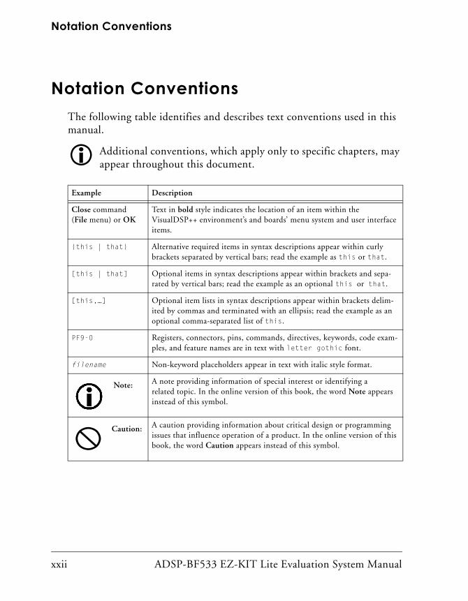
Notation Conventions
Notation ConventionsThe following table identifies and describes text conventions used in this manual.
Additional conventions, which apply only to specific chapters, may appear throughout this document.
Example Description
Close command (File menu) or OK
Text in bold style indicates the location of an item within the VisualDSP++ environment’s and boards’ menu system and user interface items.
{this | that} Alternative required items in syntax descriptions appear within curly brackets separated by vertical bars; read the example as this or that.
[this | that] Optional items in syntax descriptions appear within brackets and sepa-rated by vertical bars; read the example as an optional this or that.
[this,…] Optional item lists in syntax descriptions appear within brackets delim-ited by commas and terminated with an ellipsis; read the example as an optional comma-separated list of this.
PF9-0 Registers, connectors, pins, commands, directives, keywords, code exam-ples, and feature names are in text with letter gothic font.
filename Non-keyword placeholders appear in text with italic style format.
Note: A note providing information of special interest or identifying a related topic. In the online version of this book, the word Note appears instead of this symbol.
Caution: A caution providing information about critical design or programming issues that influence operation of a product. In the online version of this book, the word Caution appears instead of this symbol.
xxii ADSP-BF533 EZ-KIT Lite Evaluation System Manual
1 GETTING STARTED
This chapter provides the information you need to begin using
ADSP-BF533 EZ-KIT Lite evaluation system. For correct operation, install the software and hardware in the order presented in “Installation Tasks” on page 1-3.The chapter includes the following sections.
• “Contents of EZ-KIT Lite Package” on page 1-1
Provides a list of the components shipped with this EZ-KIT Lite evaluation system.
• “PC Configuration” on page 1-3
Describes the minimum requirements for the PC to work with the EZ-KIT Lite evaluation system.
• “Installation Tasks” on page 1-3
Describes the step-by-step procedures for setting up the hardware and software.
Contents of EZ-KIT Lite PackageYour ADSP-BF533 EZ-KIT Lite evaluation system package contains the following items.
• ADSP-BF533 EZ-KIT Lite board
• EZ-KIT Lite Quick Start Guide
ADSP-BF533 EZ-KIT Lite Evaluation System Manual 1-1
Contents of EZ-KIT Lite Package
• VisualDSP++ 3.5 Installation Quick Reference Card
• CD containing:
VisualDSP++ for 16-Bit Processors with a limited license
ADSP-BF533 EZ-KIT Lite debug software
USB driver files
Example programs
ADSP-BF533 EZ-KIT Lite Evaluation System Manual
• Universal 7.5V DC power supply
• USB 2.0 type cable
• Registration card (please fill out and return)
If any item is missing, contact the vendor where you purchased your EZ-KIT Lite or contact Analog Devices, Inc.
The EZ-KIT Lite evaluation system contains ESD (electrostatic discharge) sensitive devices. Electro-static charges readily accumulate on the human body and equipment and can discharge without detection. Permanent damage may occur on devices subjected to high-energy discharges. Proper ESD precautions are recommended to avoid performance degradation or loss of functionality. Store unused EZ-KIT Lite boards in the protective shipping package.
1-2 ADSP-BF533 EZ-KIT Lite Evaluation System Manual
Getting Started
PC ConfigurationFor correct operation of the VisualDSP++ software and the EZ-KIT Lite, your computer must have the minimum configuration:
EZ-KIT Lite does not run under Windows 95 or Windows NT.
Installation TasksThe following task list is provided for the safe and effective use of the ADSP-BF533 EZ-KIT Lite. Follow these instructions in the presented order to ensure correct operation of your software and hardware.
1. VisualDSP++ and EZ-KIT Lite software installation
2. VisualDSP++ license installation and registration
3. EZ-KIT Lite hardware setup
4. EZ-KIT Lite USB driver installation
5. USB driver installation verification
6. VisualDSP++ startup
Windows 98, Windows 2000, Windows XP
Intel (or comparable) 333 MHz processor
VGA Monitor and color video card
2-button mouse
200 MB free on hard drive
128 MB RAM
Full-speed USB port
CD-ROM Drive
ADSP-BF533 EZ-KIT Lite Evaluation System Manual 1-3
Installation Tasks
Installing VisualDSP++ and EZ-KIT Lite SoftwareThis EZ-KIT Lite comes with the latest version of VisualDSP++ 3.5 for 16-bit processors. VisualDSP++ installation includes EZ-KIT Lite installations.
To install VisualDSP++ and EZ-KIT Lite software:
1. Insert the VisualDSP++ installation CD into the CD-ROM drive.
2. If Autoplay is enabled on your PC, you see the Install Shield Wiz-ard Welcome screen. Otherwise, choose Run from the Start menu, and enter D:\ADI_Setup.exe in the Open field, where D is the name of your local CD-ROM drive.
3. Follow the on-screen instructions to continue installing the software.
4. At the Custom Setup screen, select your EZ-KIT Lite from the list of available systems and choose the installation directory.
Click an icon in the Feature Description field to see the selected system’s description. When you have finished, click Next.
5. At the Ready to Install screen, click Back to change your install options, click Install to install the software, or click Cancel to exit the install.
6. When the EZ-KIT Lite installs, the Wizard Completed screen appears. Click Finish.
1-4 ADSP-BF533 EZ-KIT Lite Evaluation System Manual
Getting Started
Installing and Registering VisualDSP++ LicenseVisualDSP++ and EZ-KIT Lites are licensed products. You may run only one copy of the software for each license purchased. Once a new copy of the VisualDSP++ or EZ-KIT Lite software is installed on your PC, you must install, register, and validate your licence.
The VisualDSP++ 3.5 Installation Quick Reference Card included in your package will guide you through the licence installation and registration process (refer to Tasks 1, 2, and 3).
Setting Up EZ-KIT Lite Hardware
The ADSP-BF533 EZ-KIT Lite board is designed to run outside your per-sonal computer as a stand-alone unit. You do not have to open your computer case.
To connect the EZ-KIT Lite board:
1. Remove the EZ-KIT Lite board from the package. Be careful when handling the board to avoid the discharge of static electricity, which may damage some components.
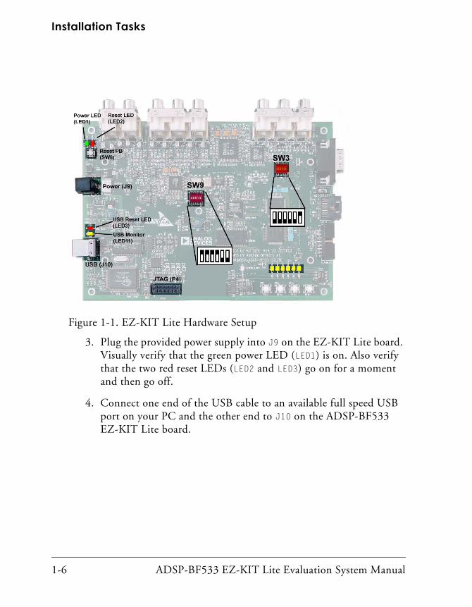
2. Figure 1-1 shows the default jumper settings, DIP switch, connec-tor locations, and LEDs used in installation. Confirm that your board is set up in the default configuration before continuing.
The EZ-KIT Lite evaluation system contains ESD (electrostatic discharge) sensitive devices. Electrostatic charges readily accumulate on the human body and equipment and can discharge without detection. Per-manent damage may occur on devices subjected to high-energy discharges. Proper ESD precautions are recommended to avoid performance degradation or loss of functionality. Store unused EZ-KIT Lite boards in the protective shipping package.
ADSP-BF533 EZ-KIT Lite Evaluation System Manual 1-5
Installation Tasks
3. Plug the provided power supply into J9 on the EZ-KIT Lite board. Visually verify that the green power LED (LED1) is on. Also verify that the two red reset LEDs (LED2 and LED3) go on for a moment and then go off.
4. Connect one end of the USB cable to an available full speed USB port on your PC and the other end to J10 on the ADSP-BF533 EZ-KIT Lite board.
Figure 1-1. EZ-KIT Lite Hardware Setup
1-6 ADSP-BF533 EZ-KIT Lite Evaluation System Manual
Getting Started
Installing EZ-KIT Lite USB DriverThe EZ-KIT Lite evaluation system installed on the following platforms requires one full-speed USB port.
• “Windows 98 USB Driver” on page 1-8 describes the installation on Windows 98.
• “Windows 2000 USB Driver” on page 1-12 describes the installa-tion on Windows 2000.
• “Windows XP USB Driver” on page 1-13 describes the installation on Windows XP.
The USB driver used by the debug agent is not Microsoft certified because it is intended for a development or laboratory environment, not a com-mercial environment.
ADSP-BF533 EZ-KIT Lite Evaluation System Manual 1-7
Installation Tasks
Windows 98 USB Driver
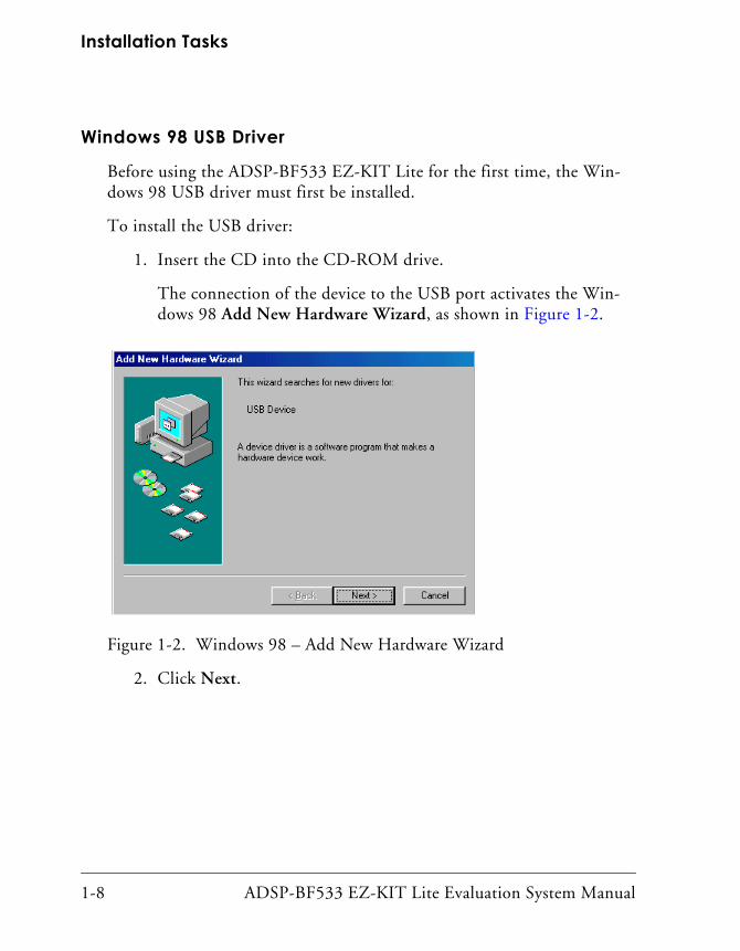
Before using the ADSP-BF533 EZ-KIT Lite for the first time, the Win-dows 98 USB driver must first be installed.
To install the USB driver:
1. Insert the CD into the CD-ROM drive.
The connection of the device to the USB port activates the Win-dows 98 Add New Hardware Wizard, as shown in Figure 1-2.
2. Click Next.
Figure 1-2. Windows 98 – Add New Hardware Wizard
1-8 ADSP-BF533 EZ-KIT Lite Evaluation System Manual
Getting Started
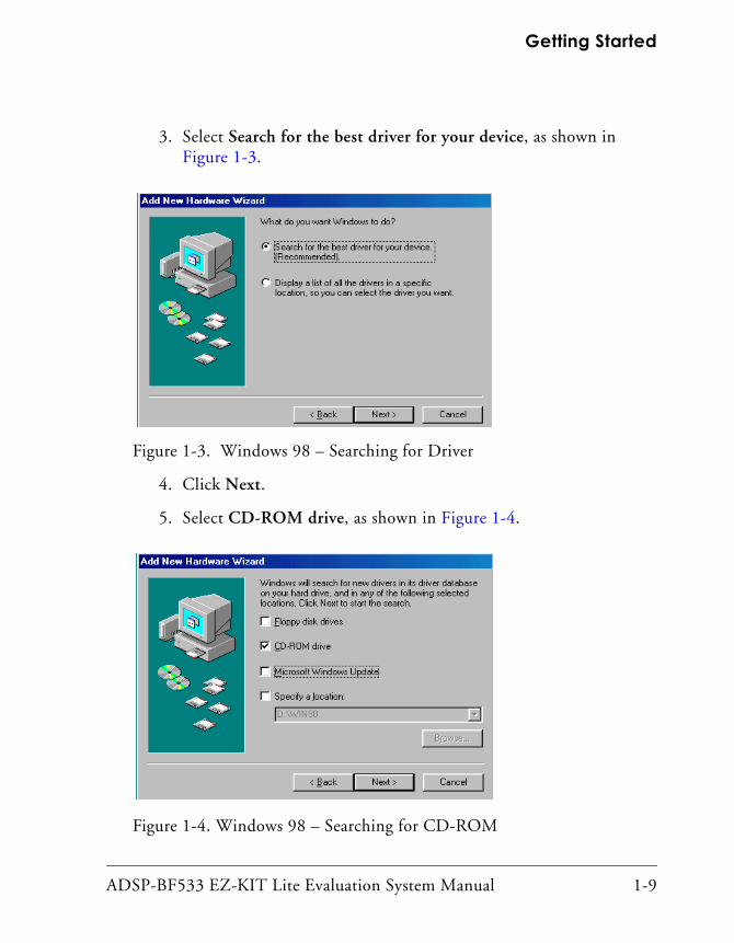
3. Select Search for the best driver for your device, as shown in Figure 1-3.
4. Click Next.
5. Select CD-ROM drive, as shown in Figure 1-4.
Figure 1-3. Windows 98 – Searching for Driver
Figure 1-4. Windows 98 – Searching for CD-ROM
ADSP-BF533 EZ-KIT Lite Evaluation System Manual 1-9

Installation Tasks
6. Click Next. Windows 98 locates the WmUSBEz.inf file on the installation CD, as shown in Figure 1-5.
7. Click Next.The Coping Files dialog box appears (Figure 1-6).
Figure 1-5. Windows 98 – Locating Driver
Figure 1-6. Windows 98 – Searching for .SYS File
1-10 ADSP-BF533 EZ-KIT Lite Evaluation System Manual
Getting Started
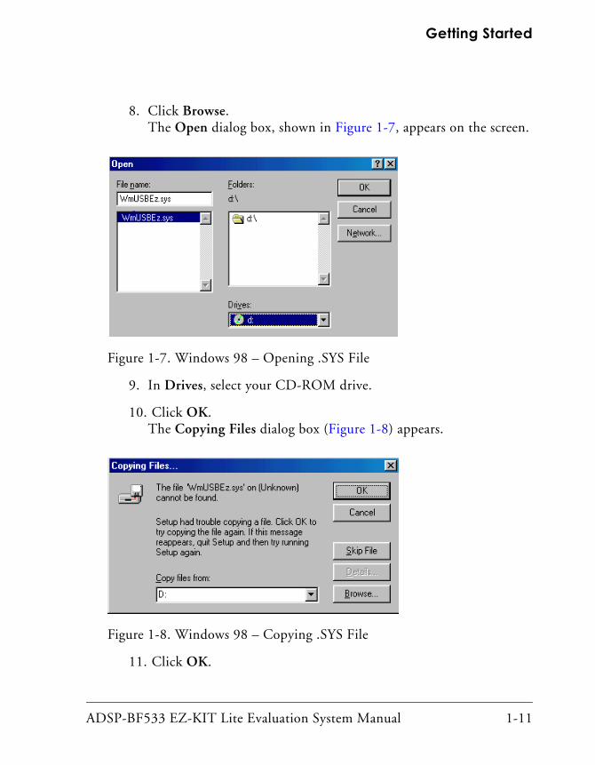
8. Click Browse. The Open dialog box, shown in Figure 1-7, appears on the screen.
9. In Drives, select your CD-ROM drive.
10. Click OK.The Copying Files dialog box (Figure 1-8) appears.
11. Click OK.
Figure 1-7. Windows 98 – Opening .SYS File
Figure 1-8. Windows 98 – Copying .SYS File
ADSP-BF533 EZ-KIT Lite Evaluation System Manual 1-11
Installation Tasks
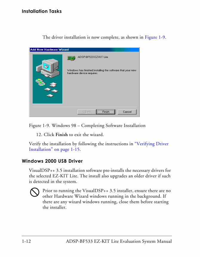
The driver installation is now complete, as shown in Figure 1-9.
12. Click Finish to exit the wizard.
Verify the installation by following the instructions in “Verifying Driver Installation” on page 1-15.
Windows 2000 USB Driver
VisualDSP++ 3.5 installation software pre-installs the necessary drivers for the selected EZ-KIT Lite. The install also upgrades an older driver if such is detected in the system.
Prior to running the VisualDSP++ 3.5 installer, ensure there are no other Hardware Wizard windows running in the background. If there are any wizard windows running, close them before starting the installer.
Figure 1-9. Windows 98 – Completing Software Installation
1-12 ADSP-BF533 EZ-KIT Lite Evaluation System Manual
Getting Started
To install the USB driver:
1. If VisualDSP++ 3.5 is already installed on your system, go to step 2. Otherwise, run VisualDSP++ 3.5 installation. Refer to the VisualDSP++ 3.5 Installation Quick Reference Card for a detailed installation description.When installing VisualDSP++ 3.5 on Windows 2000, make sure the appropriate EZ-KIT Lite component is selected for the installation.
2. Connect the EZ-KIT Lite device to your PC’s USB port. Windows 2000 automatically detects an EZ-KIT device and auto-matically installs the appropriate driver for the selected device (see step 1).
3. Verify the installation by following the instructions in “Verifying Driver Installation” on page 1-15.
Windows XP USB Driver
VisualDSP++ 3.5 installation software pre-installs the necessary drivers for the selected EZ-KIT Lite. The install also upgrades an older driver if such is detected in the system.
Prior to running the VisualDSP++ 3.5 installer, ensure there are no other Hardware Wizard windows running in the background. If there are any wizard windows running, close them before starting the installer.
To install the USB driver:
1. If VisualDSP++ 3.5 is already installed on your system, go to step 2. Otherwise, run VisualDSP++ 3.5 installation. Refer to the VisualDSP++ 3.5 Installation Quick Reference Card for a detailed installation description.When installing VisualDSP++ 3.5 on Windows XP, make sure the appropriate EZ-KIT Lite component is selected for the installation.
ADSP-BF533 EZ-KIT Lite Evaluation System Manual 1-13
Installation Tasks
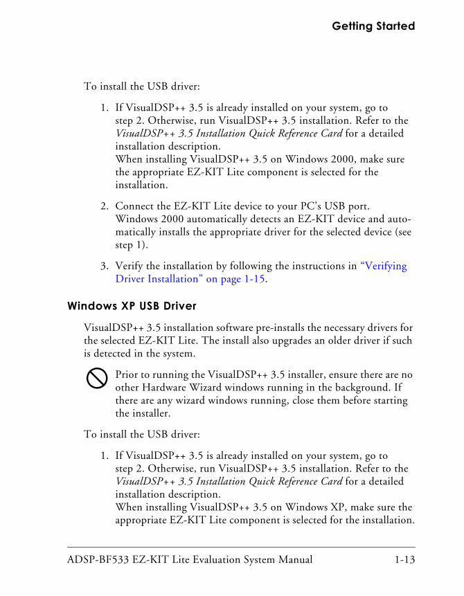
2. Connect the EZ-KIT Lite device to your PC’s USB port. By connecting the device to the USB port you activate the Win-dows XP Found New Hardware Wizard, shown in Figure 1-10.
Figure 1-10. Windows XP – Found New Hardware Wizard
1-14 ADSP-BF533 EZ-KIT Lite Evaluation System Manual
Getting Started
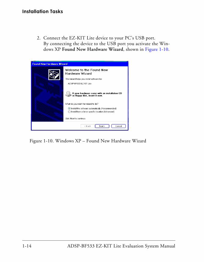
3. Select Install the software automatically (Recommended) and click Next.When Windows XP completes the driver installation for the selected device (see step 1), a window shown in Figure 1-11 appears on the screen.
4. Verify the installation by following the instructions in “Verifying Driver Installation”.
Verifying Driver InstallationBefore using the EZ-KIT Lite evaluation system, verify that the USB driver software is installed properly:
1. Ensure that the USB cable is connected to the evaluation board and the PC.
2. Verify that the yellow USB monitor LED (LED11) is lit. This signi-fies that the board is communicating properly with the host PC and is ready to run VisualDSP++.
Figure 1-11. Windows XP – Completing Driver Installation
ADSP-BF533 EZ-KIT Lite Evaluation System Manual 1-15
Installation Tasks
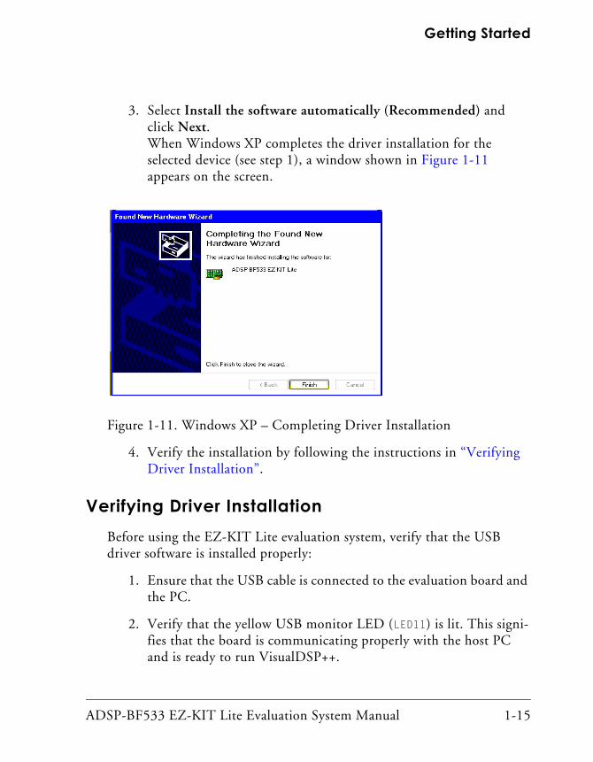
3. Verify that the USB driver software is installed properly.Open Windows Device Manager and verify that ADSP-BF533 EZ-KIT Lite shows under ADI Development Tools with no excla-mation point, as in Figure 1-12.
If using an EZ-KIT Lite on Windows 98, disconnect the USB cable from the board before booting the PC. When Windows 98 is booted and you are logged on, re-connect the USB cable to the board. The operation should continue normally from this point.
Starting VisualDSP++To set up a session in VisualDSP++:
1. Verify that the yellow USB monitor LED (LED11, located near the USB connector) is lit. This signifies that the board is communicat-ing properly with the host PC and is ready to run VisualDSP++.
2. Hold down the Control (CTRL) key.
Figure 1-12. Device Manager Window
1-16 ADSP-BF533 EZ-KIT Lite Evaluation System Manual
Getting Started
3. Select the Start button on the Windows taskbar, then choose Pro-grams, Analog Devices, VisualDSP++ 3.5 for 16-bit Processors, VisualDSP++ Environment.
If you are running VisualDSP++ for the first time, go to step 4. If you already have existing sessions, the Session List dialog box appears on the screen.
4. Click New Session.
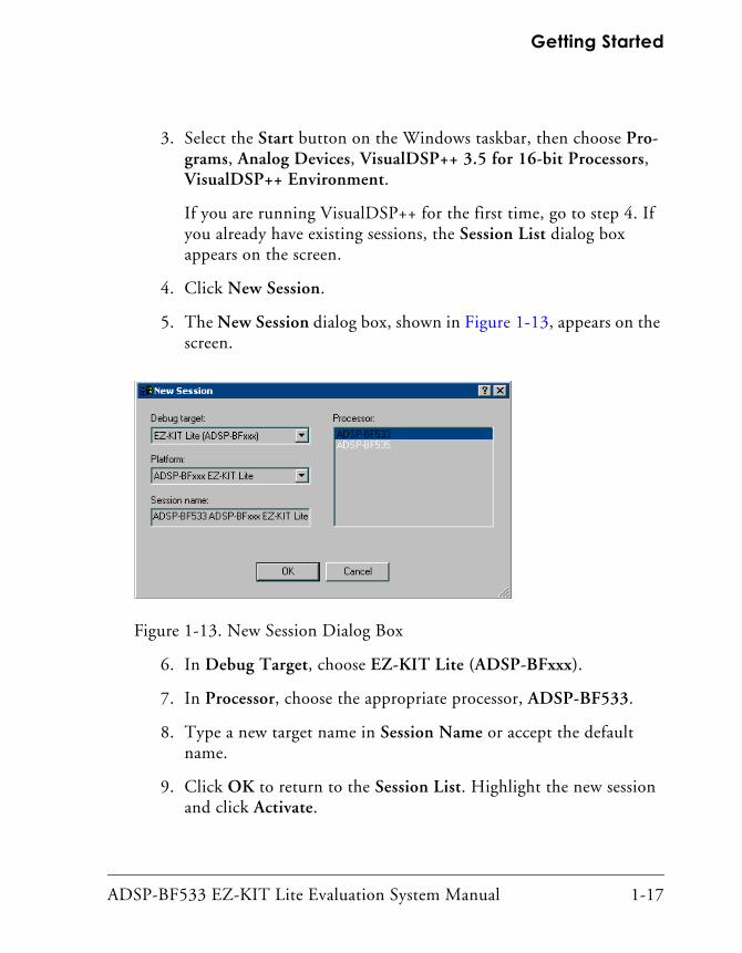
5. The New Session dialog box, shown in Figure 1-13, appears on the screen.
6. In Debug Target, choose EZ-KIT Lite (ADSP-BFxxx).
7. In Processor, choose the appropriate processor, ADSP-BF533.
8. Type a new target name in Session Name or accept the default name.
9. Click OK to return to the Session List. Highlight the new session and click Activate.
Figure 1-13. New Session Dialog Box
ADSP-BF533 EZ-KIT Lite Evaluation System Manual 1-17
Installation Tasks
1-18 ADSP-BF533 EZ-KIT Lite Evaluation System Manual
2 USING EZ-KIT LITE
This chapter provides specific information to assist you with developing
programs for the ADSP-BF533 EZ-KIT Lite evaluation system. The information appears in the following sections.• “EZ-KIT Lite License Restrictions” on page 2-2
Describes the restrictions of the VisualDSP++ license shipped with the EZ-KIT Lite.
• “Memory Map” on page 2-2
Defines the ADSP-BF533 EZ-KIT Lite board’s memory map.
• “Using SDRAM Interface” on page 2-4·
Defines the register values to configure the on-board SDRAM.
• “Using Flash Memory” on page 2-5
Describes the on-board Flash memory.
• “Example Programs” on page 2-13
Provides information about the example programs included in the ADSP-BF533 EZ-KIT Lite evaluation system.
• “Using Background Telemetry Channel” on page 2-13
Highlights the advantages of the Background Telemetry Channel feature of VisualDSP++.
• “Using EZ-KIT Lite VisualDSP++ Interface” on page 2-13
ADSP-BF533 EZ-KIT Lite Evaluation System Manual 2-1
EZ-KIT Lite License Restrictions
Describes the trace, performance monitoring, boot loading, con-text switching, and target options facilities of the EZ-KIT Lite system.
For more detailed information about programming the ADSP-BF533 Blackfin processor, see the documents referred to as “Related Documents”.
EZ-KIT Lite License RestrictionsThe license shipped with the EZ-KIT Lite imposes the following restrictions.
• The size of a user program is limited to 20 KB of the ADSP-BF533 processor’s internal memory space.
• No connections to simulator or emulator sessions are allowed.
• The EZ-KIT Lite hardware must be connected and powered up in order to use VisualDSP++ with a kit license.
Memory MapThe ADSP-BF533 processor has internal SRAM that can be used for instruction or data storage. The configuration of internal SRAM is detailed in the ADSP-BF533 Processor Hardware Reference.
The ADSP-BF533 EZ-KIT Lite board includes two types of external memory, SDRAM and Flash memory.
The size of the SDRAM is 32 Mbytes (16M x 16-bit). The processor’s memory select pin ~SMS0 is configured for the SDRAM.
2-2 ADSP-BF533 EZ-KIT Lite Evaluation System Manual
Using EZ-KIT Lite
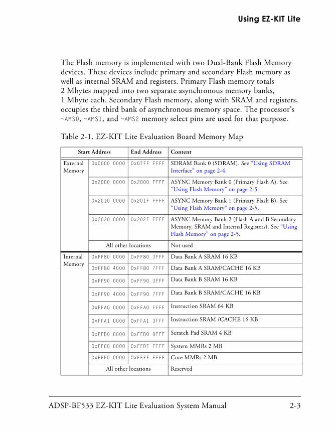
The Flash memory is implemented with two Dual-Bank Flash Memory devices. These devices include primary and secondary Flash memory as well as internal SRAM and registers. Primary Flash memory totals 2 Mbytes mapped into two separate asynchronous memory banks, 1 Mbyte each. Secondary Flash memory, along with SRAM and registers, occupies the third bank of asynchronous memory space. The processor’s ~AMS0, ~AMS1, and ~AMS2 memory select pins are used for that purpose.
Table 2-1. EZ-KIT Lite Evaluation Board Memory Map
Start Address End Address Content
External Memory
0x0000 0000 0x07FF FFFF SDRAM Bank 0 (SDRAM). See “Using SDRAM Interface” on page 2-4.
0x2000 0000 0x2000 FFFF ASYNC Memory Bank 0 (Primary Flash A). See “Using Flash Memory” on page 2-5.
0x2010 0000 0x201F FFFF ASYNC Memory Bank 1 (Primary Flash B). See “Using Flash Memory” on page 2-5.
0x2020 0000 0x202F FFFF ASYNC Memory Bank 2 (Flash A and B Secondary Memory, SRAM and Internal Registers). See “Using Flash Memory” on page 2-5.
All other locations Not used
Internal Memory
0xFF80 0000 0xFF80 3FFF Data Bank A SRAM 16 KB
0xFF80 4000 0xFF80 7FFF Data Bank A SRAM/CACHE 16 KB
0xFF90 0000 0xFF90 3FFF Data Bank B SRAM 16 KB
0xFF90 4000 0xFF90 7FFF Data Bank B SRAM/CACHE 16 KB
0xFFA0 0000 0xFFA0 FFFF Instruction SRAM 64 KB
0xFFA1 0000 0xFFA1 3FFF Instruction SRAM /CACHE 16 KB
0xFFB0 0000 0xFFBO 0FFF Scratch Pad SRAM 4 KB
0xFFC0 0000 0xFFDF FFFF System MMRs 2 MB
0xFFE0 0000 0xFFFF FFFF Core MMRs 2 MB
All other locations Reserved
ADSP-BF533 EZ-KIT Lite Evaluation System Manual 2-3

Using SDRAM Interface
Using SDRAM InterfaceThe three SDRAM control registers must be initialized in order to use the MT48LC4M16ATG-75 16M x 16 bits (32 MB) SDRAM memory. When you are in a VisualDSP++ EZ-KIT Lite session (that is, using the USB debug interface and not using an emulator), the SDRAM registers are con-figured automatically through the debugger. The values in Table 2-2 are used whenever Bank 0 is accessed through the debugger (for example, when viewing memory windows or loading a program). The numbers were derived for maximum flexibility and work for a system clock frequency between 54 MHz and 133 MHz.
The EBIU_SDGCTL register can only be re-written within the user code by first placing the chip in self refresh (see the ADSP-BF533 Blackfin Proces-sor Hardware Reference). Clearing the appropriate checkbox on the Target
Table 2-2. EZ-KIT Lite Session SDRAM Default Settings1
1 54 MHz <= SCLK <= 133 MHz.
Register Value Function
EBIU_SDGCTL 0x0091998D Calculated with SCLK = 133 MHz16-bit data pathExternal buffering timing disabledtWR = 2 SCLK cycles
tRCD = 3 SCLK cycles
tRP = 3 SCLK cycles
tRAS = 6 SCLK cycles
pre-fetch disabledCAS latency = 3 SCLK cyclesSCLK1 disabled
EBIU_SDBCTL 0x00000013 Bank 0 enabledBank 0 size = 32 MBBank 0 column address width = 9 bits
EBIU_SDRRC 0x000001A0 Calculated with SCLK = 54 MHzRDIV = 416 clock cycles
2-4 ADSP-BF533 EZ-KIT Lite Evaluation System Manual
Using EZ-KIT Lite
Options dialog box, which is accessible through the Settings pull-down menu, disables automatic and allows manual configuration. For more information, see “Target Options” on page 2-17.
Automatic configuration of SDRAM is not optimized for any SCLK fre-quency. Table 2-3 shows the optimized configuration for the SDRAM registers using a 118.8 MHz, 126 MHz, and 133 MHz SCLK. The fre-quency of 118.8 MHz is the maximum SCLK frequency when using a 594 MHz core frequency, the maximum frequency for the EZ-KIT Lite when using the internal voltage regulator. Only the EBIU_SDRRC register needs to be modified in the user code to achieve maximum performance.
An example program is included in the EZ-KIT installation directory to demonstrate how to set up the SDRAM interface.
Using Flash MemoryThe following sections describe how to use the memory and general-pur-pose IO pins, as well as how to configure the Flash memory device.
The ADSP-BF533 EZ-KIT Lite board employs two PSD4256G6V Flash/General-Purpose IO devices from STMicroelectronics. These devices not only have Flash memory but also extra IO pins, which are memory mapped.
Table 2-3. SDRAM Optimum Settings
Register SCLK = 133 MHz(Processor MAX)
SCLK = 126 MHz(CCLK = 756 MHz)
SCLK = 118.8 MHz(CCLK = 594 MHz)
EBIU_SDGCTL 0x0091 998D 0x0091 998D 0x0091 998D
EBIU_SDBCTL 0x0000 0013 0x0000 0013 0x0000 0013
EBIU_SDRRC 0x0000 0406 0x0000 03CF 0x0000 0397
ADSP-BF533 EZ-KIT Lite Evaluation System Manual 2-5
Using Flash Memory
Example code is provided in the EZ-KIT installation directory to demon-strate how to program the Flash memory as well as to demonstrate the functionality of the general-purpose IO pins.
Flash Memory MapEach device includes the following memory segments:
• 1M byte of primary Flash memory
• 64K bytes of secondary Flash memory
• 32 Kbytes of internal SRAM
• 256 Bytes of configuration registers (IO control)
Access to each segment can be 8-bit or 16-bit. The processor’s ~AMS0, ~AMS1, and ~AMS2 memory select pin are used for that purpose. Asynchro-nous memory Bank 0 is always enabled after a hard reset, while Banks 1 and 2 need to be enabled by software. Table 2-4 provides an example on asynchronous memory configuration registers.
Each Flash chip is initially configured with the memory sectors mapped into the processor’s address space as shown in Table 2-5.
Table 2-4. Asynchronous Memory Control Registers Settings Example
Register Value Function
EBIU_AMBCTL0 0x7BB07BB0 Timing control for Banks 1 and 0
EBIU_AMBCTL1 bits 15-0 0x7BB0 Timing control for Bank 2 (Bank 3 is not used)
EBIU_AMGCTL bits 3-0 0xF Enable all banks
2-6 ADSP-BF533 EZ-KIT Lite Evaluation System Manual

Using EZ-KIT Lite
Flash General-Purpose IOThis section describes general-purpose IO signals that are controlled by means of setting appropriate registers of the Flash A or Flash B. These reg-isters are mapped into the processor’s address space, as shown in Table 2-5 on page 2-7.
Flash device IO pins are arranged as 8-bit ports labeled A through G. There is a set of 8-bit registers associated with each port. These registers are: Direction, Data In, and Data Out. Note that the Direction and Data Out registers are cleared to all zeros at power-up or hardware reset.
The Direction register controls IO pins direction. When a bit is 0, a cor-responding pin functions as an input. When a bit is 1, a corresponding pin is an output. This is a 8-bit read-write register.
The Data In register allows reading the status of port’s pins. This is a 8-bit read-only register.
Table 2-5. Flash Memory Map
Start Address End Address Content
0x2000 0000 0x200F FFFF Flash A Primary (1MB)
0x2010 0000 0x201F FFFF Flash B Primary (1MB)
0x2020 0000 0x2020 FFFF Flash A Secondary (64KB)
0x2024 0000 0x2024 7FFF Flash A SRAM (32KB)
0x2027 0000 0x2027 00FF Flash A Registers (256 Bytes)
0x2028 0000 0x2028 FFFF Flash B Secondary (64KB)
0x202C 0000 0x202C 7FFF Flash B SRAM (32KB)
0x202E 0000 0x202E 00FF Flash B Registers (256 Bytes)
All other locations Reserved
ADSP-BF533 EZ-KIT Lite Evaluation System Manual 2-7
Using Flash Memory
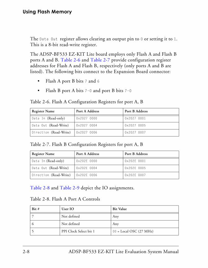
The Data Out register allows clearing an output pin to 0 or setting it to 1. This is a 8-bit read-write register.
The ADSP-BF533 EZ-KIT Lite board employs only Flash A and Flash B ports A and B. Table 2-6 and Table 2-7 provide configuration register addresses for Flash A and Flash B, respectively (only ports A and B are listed). The following bits connect to the Expansion Board connector:
• Flash A port B bits 7 and 6
• Flash B port A bits 7–0 and port B bits 7–0
Table 2-8 and Table 2-9 depict the IO assignments.
Table 2-6. Flash A Configuration Registers for port A, B
Register Name Port A Address Port B Address
Data In (Read-only) 0x2027 0000 0x2027 0001
Data Out (Read-Write) 0x2027 0004 0x2027 0005
Direction (Read-Write) 0x2027 0006 0x2027 0007
Table 2-7. Flash B Configuration Registers for port A, B
Register Name Port A Address Port B Address
Data In (Read-only) 0x202E 0000 0x202E 0001
Data Out (Read-Write) 0x202E 0004 0x202E 0005
Direction (Read-Write) 0x202E 0006 0x202E 0007
Table 2-8. Flash A Port A Controls
Bit # User IO Bit Value
7 Not defined Any
6 Not defined Any
5 PPI Clock Select bit 1 00 = Local OSC (27 MHz)
2-8 ADSP-BF533 EZ-KIT Lite Evaluation System Manual
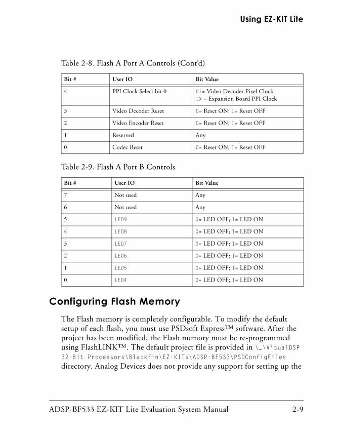
Using EZ-KIT Lite
Configuring Flash MemoryThe Flash memory is completely configurable. To modify the default setup of each flash, you must use PSDsoft Express™ software. After the project has been modified, the Flash memory must be re-programmed using FlashLINK™. The default project file is provided in \…\VisualDSP 32-Bit Processors\Blackfin\EZ-KITs\ADSP-BF533\PSDConfigFiles directory. Analog Devices does not provide any support for setting up the
4 PPI Clock Select bit 0 01= Video Decoder Pixel Clock1X = Expansion Board PPI Clock
3 Video Decoder Reset 0= Reset ON; 1= Reset OFF
2 Video Encoder Reset 0= Reset ON; 1= Reset OFF
1 Reserved Any
0 Codec Reset 0= Reset ON; 1= Reset OFF
Table 2-9. Flash A Port B Controls
Bit # User IO Bit Value
7 Not used Any
6 Not used Any
5 LED9 0= LED OFF; 1= LED ON
4 LED8 0= LED OFF; 1= LED ON
3 LED7 0= LED OFF; 1= LED ON
2 LED6 0= LED OFF; 1= LED ON
1 LED5 0= LED OFF; 1= LED ON
0 LED4 0= LED OFF; 1= LED ON
Table 2-8. Flash A Port A Controls (Cont’d)
Bit # User IO Bit Value
ADSP-BF533 EZ-KIT Lite Evaluation System Manual 2-9

Using LEDs and Push Buttons
PSD4256G6V with PSDsoft Express or programming it using FlashLINK. Email STMicroelectronics at [email protected] for technical assistance.
The PSD4256G6Vcan be re-programmed using the FlashLINK JTAG programming cable available from STMicoreclectronics (www.st.com/psd) for approximately $59. FlashLINK plugs into any PC parallel port. The PSDsoft Express development software is required to modify the DSM2150 configuration and to operate the FlashLINK cable. PSDsoft Express can be downloaded at no charge from www.st.com/psd.
Using LEDs and Push ButtonsThe EZ-KIT Lite provides four push buttons and six LEDs for gen-eral-purpose IO.
The six LEDs, labeled LED4 through LED9, are accessed via some of the general-purpose IO pins of Flash memory interface. For information on how to program the pins, see “Flash General-Purpose IO” on page 2-7.
The four general-purpose push button are labeled SW4 through SW7. A sta-tus of each individual button can be read through programmable flag (PF) inputs, PF8 through PF11. A PF reads “1” when a corresponding switch is being pressed-on. When the switch is released, the PF reads “0”. A connec-tion between the push button and PF input is established through the SW9 DIP switch. See “Push Button Enable Switch (SW9)” on page 3-12 for details.
An example program is included in the EZ-KIT installation directory to demonstrate the functionality of the LEDs and push buttons.
2-10 ADSP-BF533 EZ-KIT Lite Evaluation System Manual
Using EZ-KIT Lite
Using AudioThe AD1836 audio codec provides three channels of stereo audio output and two channels of multichannel 96 kHz input. The SPORT0 interface of the processor is linked with the stereo audio data input and output pins of the AD1836 codec. The processor is capable of transferring data to the audio codec in time-division multiplexed (TDM) or I2S mode.
The I2S mode allows the codec to operate with a 96 kHz sample rate but only allows you to use two channels of output. TDM mode can operate at a maximum of 48 kHz sample rate but allows for simultaneous use of all input and output channels. When using I2S mode, the TSCLK0 and RSCLK0 pins, as well as the TFS0 and RFS0 pins of the processor, must be tied together external to the processor. This is accomplished with the SW9 DIP switch (see “Push Button Enable Switch (SW9)” on page 3-12 for more information).
The AD1836 audio codec’s internal configuration registers are configured using the processor’s SPI port. The processor’s PF4 programmable flag pin is used as the select for this device. For information on how to configure the multichannel codec, go to www.analog.com/UploadedFiles/Datasheets/344740003AD1836_prc.pdf.
The reset for the AD1836 codec comes from the general-purpose IO pin PA0 of Flash A. For information on how to use the pin, see “Flash Gen-eral-Purpose IO” on page 2-7.
Example programs are included in the EZ-KIT installation directory to demonstrate the AD1836 codec operation.
ADSP-BF533 EZ-KIT Lite Evaluation System Manual 2-11
Using Video
Using VideoThe board supports video input and output applications. The ADV7171 video encoder provides up to three output channels of analog video, while the ADV7183 video decoder provides up to three input channels of analog video. Both the encoder and the decoder connect to the Parallel Peripheral Interface (PPI) of the ADSP-BF533 processor. For additional information on the video interface hardware, refer to “PPI Interface” on page 3-5.
For the video interface to be operational, the following basic steps must be performed.
1. Configure the SW3 DIP switch as required by the application. Refer to “Video Configuration Switch (SW3)” on page 3-11 for details.
2. Remove reset to the video device. Refer to “Flash General-Purpose IO” on page 2-7 for details.
3. If using the decoder:
Enable device by driving programmable flag output PF2 to “0”.Select PPI clock (see Table 2-8 on page 2-8).
4. Program internal registers of the video device in use. Both video encoder and decoder use a 2-wire serial interface to access internal registers. A programmable flag PF0 functions as a serial clock (SCL), and PF1 functions as a serial data (SDAT).
5. Program the ADSP-BF533 processor’s PPI interface (configuration registers, DMA, etc.).
Example programs are included in the EZ-KIT installation directory to demonstrate the capabilities of the video interface.
2-12 ADSP-BF533 EZ-KIT Lite Evaluation System Manual
Using EZ-KIT Lite
Example ProgramsExample programs are provided with the ADSP-BF533 EZ-KIT Lite to demonstrate various capabilities of the evaluation board. These programs are installed with the EZ-KIT Lite software and can be found in \…\Visu-alDSP 16-bit Processors\Blackfin\EZ-KITs\ADSP-BF533\Examples. Please refer to the readme file provided with each example for more information.
Using Background Telemetry ChannelThe ADSP-BF533 USB debug agent supports the Background Telemetry Channel (BTC), which facilitates data exchange between VisualDSP++ and the processor without interrupting DSP execution.
The BTC allows the user to view a variable as it is updated or changed, all while the processor continues to execute. For increased performance of the BTC, including faster reading and writing, please check out our latest line of DSP emulators at www.analog.com/Analog_Root/productPage/productHome/0,2121,EMULA-
TORS,00.html. For more information about the Background Telemetry Channel, see the VisualDSP++ 3.5 User’s Guide for 16-Bit Processors or online Help.
Using EZ-KIT Lite VisualDSP++ InterfaceThis section provides information on the following parts of the Visu-alDSP++ graphical user interface:
• “Trace Window” on page 2-14
• “Performance Monitor” on page 2-15
• “Boot Load” on page 2-16
ADSP-BF533 EZ-KIT Lite Evaluation System Manual 2-13
Using EZ-KIT Lite VisualDSP++ Interface
• “Target Options” on page 2-17
• “Restricted Software Breakpoints” on page 2-19
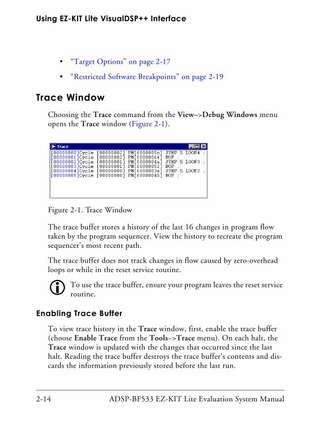
Trace WindowChoosing the Trace command from the View–>Debug Windows menu opens the Trace window (Figure 2-1).
The trace buffer stores a history of the last 16 changes in program flow taken by the program sequencer. View the history to recreate the program sequencer’s most recent path.
The trace buffer does not track changes in flow caused by zero-overhead loops or while in the reset service routine.
To use the trace buffer, ensure your program leaves the reset service routine.
Enabling Trace Buffer
To view trace history in the Trace window, first, enable the trace buffer (choose Enable Trace from the Tools–>Trace menu). On each halt, the Trace window is updated with the changes that occurred since the last halt. Reading the trace buffer destroys the trace buffer’s contents and dis-cards the information previously stored before the last run.
Figure 2-1. Trace Window
2-14 ADSP-BF533 EZ-KIT Lite Evaluation System Manual

Using EZ-KIT Lite
Reading Trace Buffer Data
The first column between the square brackets (in blue) indicates the line number in the Trace window.
The second column between square brackets, which comes in vertical pairs, shows the trace number. For each discontinuity, the first (top posi-tion) is the source trace, and the second (bottom position) is the destination trace. The third column in between square brackets shows the addresses of the instructions. Each address is followed by the assembly instruction.
The trace grows upward. In Figure 2-1 on page 2-14, trace 0 occurred before trace 1, which occurred before trace 2, and so on.
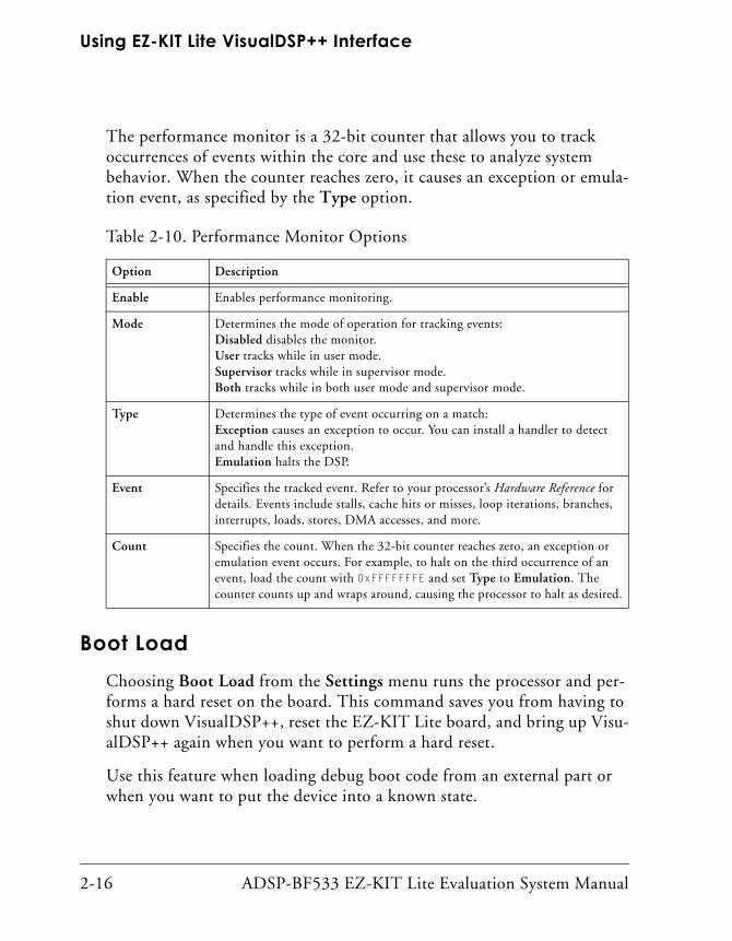
Performance MonitorChoosing Performance Monitor from the Settings menu opens the Per-formance Monitor Control dialog box shown in Figure 2-2. A description of the dialog box appears in Table 2-10 on page 2-16.
Figure 2-2. Performance Monitor Dialog Box
ADSP-BF533 EZ-KIT Lite Evaluation System Manual 2-15
Using EZ-KIT Lite VisualDSP++ Interface
The performance monitor is a 32-bit counter that allows you to track occurrences of events within the core and use these to analyze system behavior. When the counter reaches zero, it causes an exception or emula-tion event, as specified by the Type option.
Boot LoadChoosing Boot Load from the Settings menu runs the processor and per-forms a hard reset on the board. This command saves you from having to shut down VisualDSP++, reset the EZ-KIT Lite board, and bring up Visu-alDSP++ again when you want to perform a hard reset.
Use this feature when loading debug boot code from an external part or when you want to put the device into a known state.
Table 2-10. Performance Monitor Options
Option Description
Enable Enables performance monitoring.
Mode Determines the mode of operation for tracking events:Disabled disables the monitor.User tracks while in user mode.Supervisor tracks while in supervisor mode.Both tracks while in both user mode and supervisor mode.
Type Determines the type of event occurring on a match:Exception causes an exception to occur. You can install a handler to detect and handle this exception.Emulation halts the DSP.
Event Specifies the tracked event. Refer to your processor’s Hardware Reference for details. Events include stalls, cache hits or misses, loop iterations, branches, interrupts, loads, stores, DMA accesses, and more.
Count Specifies the count. When the 32-bit counter reaches zero, an exception or emulation event occurs. For example, to halt on the third occurrence of an event, load the count with 0xFFFFFFFE and set Type to Emulation. The counter counts up and wraps around, causing the processor to halt as desired.
2-16 ADSP-BF533 EZ-KIT Lite Evaluation System Manual
Using EZ-KIT Lite
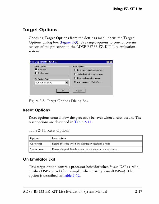
Target OptionsChoosing Target Options from the Settings menu opens the Target Options dialog box (Figure 2-3). Use target options to control certain aspects of the processor on the ADSP-BF533 EZ-KIT Lite evaluation system.
Reset Options
Reset options control how the processor behaves when a reset occurs. The reset options are described in Table 2-11.
On Emulator Exit
This target option controls processor behavior when VisualDSP++ relin-quishes DSP control (for example, when exiting VisualDSP++). The option is described in Table 2-12.
Figure 2-3. Target Options Dialog Box
Table 2-11. Reset Options
Option Description
Core reset Resets the core when the debugger executes a reset.
System reset Resets the peripherals when the debugger executes a reset.
ADSP-BF533 EZ-KIT Lite Evaluation System Manual 2-17
Using EZ-KIT Lite VisualDSP++ Interface
Other Options
Table 2-13 describes other available target options.
Table 2-12. On Emulator Exit Target Options
Option Description
On Emulator Exit Determines the state the DSP is left in when the emulator relinquishes con-trol of the DSP:Reset DSP and Run causes the DSP to reset and begin execution from its reset vector location.Run from current PC causes the DSP to begin running from its current location. Stall the DSP resets the DSP and then writes a JUMP 0 to the first location in internal memory so the DSP is stuck in a tight loop after exiting.
Table 2-13. Miscellaneous Target Options
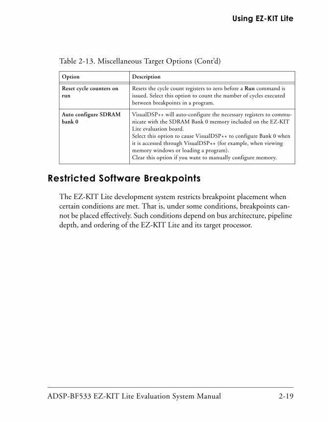
Option Description
Reset before loading exe-cutable
Resets registers before loading a DSP executable. Clear this option when DSP registers must not change to their reset values when a file load occurs.
Verify all writes to target memory
Validates all memory writes to the DSP. After each write, a read is performed and the values are checked for a matching condition.Enable this option during initial program development to locate and fix initial build problems (such as attempting to load data into non-existent memory). Clear this option to increase performance while loading executable files, since VisualDSP++ does not perform the extra reads that are required to verify each write.
2-18 ADSP-BF533 EZ-KIT Lite Evaluation System Manual
Using EZ-KIT Lite
Restricted Software Breakpoints
The EZ-KIT Lite development system restricts breakpoint placement when certain conditions are met. That is, under some conditions, breakpoints can-not be placed effectively. Such conditions depend on bus architecture, pipeline depth, and ordering of the EZ-KIT Lite and its target processor.
Reset cycle counters on run
Resets the cycle count registers to zero before a Run command is issued. Select this option to count the number of cycles executed between breakpoints in a program.
Auto configure SDRAM bank 0
VisualDSP++ will auto-configure the necessary registers to commu-nicate with the SDRAM Bank 0 memory included on the EZ-KIT Lite evaluation board.Select this option to cause VisualDSP++ to configure Bank 0 when it is accessed through VisualDSP++ (for example, when viewing memory windows or loading a program). Clear this option if you want to manually configure memory.
Table 2-13. Miscellaneous Target Options (Cont’d)
Option Description
ADSP-BF533 EZ-KIT Lite Evaluation System Manual 2-19
Using EZ-KIT Lite VisualDSP++ Interface
2-20 ADSP-BF533 EZ-KIT Lite Evaluation System Manual
3 EZ-KIT LITE HARDWARE REFERENCE
This chapter describes the hardware design of the ADSP-BF533 EZ-KIT
Lite board. The following topics are covered.• “System Architecture” on page 3-2
Describes the configuration of the ADSP-BF533 EZ-KIT Lite board and explains how the board components interface with the processor.
• “Jumper and DIP Switch Settings” on page 3-9
Shows the location and describes the function of the configuration jumpers and DIP switches.
• “LEDs and Push Buttons” on page 3-13
Shows the location and describes the function of the LEDs and push buttons.
• “Connectors” on page 3-16
Shows the location and gives the part number for all of the con-nectors on the board. Also, the manufacturer and part number information is given for the mating parts.
ADSP-BF533 EZ-KIT Lite Evaluation System Manual 3-1
System Architecture
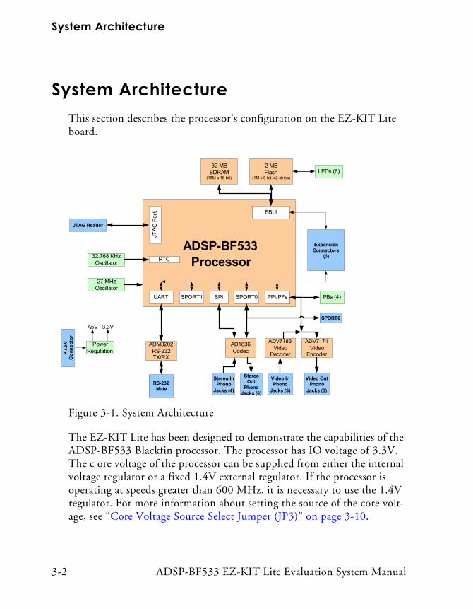
System ArchitectureThis section describes the processor’s configuration on the EZ-KIT Lite board.
The EZ-KIT Lite has been designed to demonstrate the capabilities of the ADSP-BF533 Blackfin processor. The processor has IO voltage of 3.3V. The c ore voltage of the processor can be supplied from either the internal voltage regulator or a fixed 1.4V external regulator. If the processor is operating at speeds greater than 600 MHz, it is necessary to use the 1.4V regulator. For more information about setting the source of the core volt-age, see “Core Voltage Source Select Jumper (JP3)” on page 3-10.
Figure 3-1. System Architecture
ADSP-BF533Processor
AD1836Codec
JTAG Header
PowerRegulation
LEDs (6)
EBUI
JTA G
Port
A5V
+7.5
VC
onne
ctor
32.768 KHzOscillator RTC
SPI
32 MBSDRAM
(16M x 16-bit)
ExpansionConnectors
(3)
2 MBFlash
(1M x 8-bit x 2-chips)
27 MHzOscillator
ADV7183Video
Decoder
ADV7171Video
Encoder
Video OutPhono
Jacks (3)
Video InPhono
Jacks (3)
3.3V
StereoOut
PhonoJacks (6)
Stereo InPhono
Jacks (4)
UART SPORT1 PBs (4)
RS-232Male
ADM3202RS-232TX/RX
SPORT0 PPI/PFs
SPORT0
3-2 ADSP-BF533 EZ-KIT Lite Evaluation System Manual
EZ-KIT Lite Hardware Reference
The core voltage and the core clock rate can be set on the fly by the pro-cessor. The input clock is 27 MHz. A 32.768 kHz crystal supplies the Real Time Clock (RTC) inputs of the processor. The default mode for the pro-cessor is Flash boot. See “Boot Mode Select Jumpers (JP2–1)” on page 3-10 for information about changing the default boot mode.
External Bus Interface UnitThe External Bus Interface Unit (EBIU) connects an external memory to the ADSP-BF533 device. It includes a 16-bit wide data bus, an address bus, and a control bus. Both 16-bit and 8-bit access are supported. On the EZ-KIT Lite, the EBI unit connects to SDRAM and Flash memory.
32 Mbytes (16M x 16 bits) of SDRAM connect to the synchronous mem-ory select 0 pin (~SMS0). Refer to “Using SDRAM Interface” on page 2-4 for information about configuring the SDRAM. Note that SDRAM clock is the processor’s Clock Out (CLK OUT), which frequency should not exceed 133 MHz.
Two Flash memory devices are connected to the asynchronous memory select signals, ~AMS2 through ~AMS0. The devices provide total of 2 Mbytes of primary Flash memory, 128 Kbytes of secondary Flash memory, and 64 Kbytes of SRAM. The processor can use this memory for both booting and storing information during normal operation. Refer to “Using Flash Memory” on page 2-5 for details.
All of the address, data, and control signals are available externally via the extender connectors P3–1. The pinout of these connectors can be found in Appendix B, “Schematics” on page B-1.
ADSP-BF533 EZ-KIT Lite Evaluation System Manual 3-3
System Architecture
SPORT0 Audio InterfaceThe SPORT0 interface is connected to the AD1836 audio codec, the SPORT connector (P3), and the expansion interface. The AD1836 codec uses both the primary and secondary data transmit and receive pins to input and output data from the audio input and outputs.
The pinout of the SPORT connector and the expansion interface connec-tors can be found in Appendix B, “Schematics” on page B-1.
SPI InterfaceThe processor’s Serial Peripheral Interconnect (SPI) interface is connected to the AD1836 audio codec and the expansion interface. The SPI connec-tion to the AD1836 is used to access the control registers of the device. The PF4 flag of the processor is used as the devices select for the SPI port.
Programmable Flags
The processor has 15 programmable flag pins (PFs). The pins have multi-ple functions, depending on the setup of the processor. Table 3-1 shows how the programmable flag pins are used on the EZ-KIT Lite.
Table 3-1. Programmable Flag Connections
DSP PF Pin Other DSP Function EZ-KIT Function
PF0 Serial clock for programming ADV7171 and ADV7183
PF1 Serial data for programming ADV7171 and ADV7183
PF2 ADV7183 ~OE
PF3 FS3 ADV7183 Field Pin. See “Video Configuration Switch (SW3)” on page 3-11.
PF4 AD1836 SPI Select
3-4 ADSP-BF533 EZ-KIT Lite Evaluation System Manual
EZ-KIT Lite Hardware Reference
PPI InterfaceThe Parallel Peripheral Interface (PPI) of the ADSP-BF533 processor is a half-duplex, bi-directional port that can accommodate up to 16 bits of data. The interface has a dedicated input clock (27 MHz), three multi-plexed frame sync signals, and four bits of dedicated data. The remaining data bits come from re-configured programmable flag pins. For informa-
PF5
PF6
PF7
PF8 Push button (SW4). See “Using LEDs and Push But-tons” on page 2-10 and “Push Button Enable Switch (SW9)” on page 3-12 for information on how to dis-able the push button.
PF9 Push button (SW5). See “Using LEDs and Push But-tons” on page 2-10 and “Push Button Enable Switch (SW9)” on page 3-12 for information on how to dis-able the push button.
PF10 Push button (SW6). See “Using LEDs and Push But-tons” on page 2-10 and “Push Button Enable Switch (SW9)” on page 3-12 for information on how to dis-able the push button.
PF11 Push button (SW7). See “Using LEDs and Push But-tons” on page 2-10 and “Push Button Enable Switch (SW9)” on page 3-12 for information on how to dis-able the push button.
PF12 PPI7 ADV7171 and ADV7183 Data (MSB)
PF13 PPI6 ADV7171 and ADV7183 Data
PF14 PPI5 ADV7171 and ADV7183 Data
PF15 PPI4 ADV7171 and ADV7183 Data
Table 3-1. Programmable Flag Connections (Cont’d)
DSP PF Pin Other DSP Function EZ-KIT Function
ADSP-BF533 EZ-KIT Lite Evaluation System Manual 3-5
System Architecture
tion about the pins, which multiplexed with the PPI, see “Programmable Flags” on page 3-4. For information about the ADSP-BF533 processor PPI interface, refer to the ADSP-BF533 Blackfin Processor Hardware Refer-ence. Table 3-2 describes the PPI pins and their use on the EZ-KIT Lite board.
The ADSP-BF533 EZ-KIT Lite board employs 8-bit PPI interface for video output and video input.
Table 3-2. PPI Connections
DSP PPI Pin Other DSP Function EZ-KIT Function
PPI7 PF12 ADV7171 and ADV7183 Data (MSB)
PPI6 PF13 ADV7171 and ADV7183 Data
PPI5 PF14 ADV7171 and ADV7183 Data
PPI4 PF15 ADV7171 and ADV7183 Data
PPI3 ADV7171 and ADV7183 Data
PPI2 ADV7171 and ADV7183 Data
PPI1 ADV7171 and ADV7183 Data
PPI0 ADV7171 and ADV7183 Data
PF3 FS3 ADV7183 Field Pin. For more information, see “Video Configuration Switch (SW3)” on page 3-11.
TMR1 PPI_HSYNC ADV7171 and ADV7183 HSYNC. For more information, see “Video Configuration Switch (SW3)” on page 3-11.
TMR2 PPI_FSYNC ADV7171 and ADV7183 VSYNC. For more information, see “Video Configuration Switch (SW3)” on page 3-11.
PPI_CLK Input from either the ADV7183 output clock or the same 27 MHz oscillator driving the pro-cessor. For more information, see “Using Video” on page 2-12.
3-6 ADSP-BF533 EZ-KIT Lite Evaluation System Manual
EZ-KIT Lite Hardware Reference
Video Output Mode
In the video output mode, the PPI interface is configured as output and connects to the on-board video encoder device, ADV7171. The ADV7171 encoder device generates three analog video channels on DAC B, DAC C, and DAC D outputs. The PPI data connects to P7–0 of the encoder’s pixel inputs. The encoder’s PPI input clock runs at 27 MHz, and it is in phase with CLK IN of the ADSP-BF533 processor.
The encoder’s synchronization signals, HSYNC and VSYNC, can be config-ured as inputs or outputs. Video Blanking control signal is at level “1”. The HSYNC and VSYNC signals can be connected to the ADSP-BF533 pro-cessor’s multiplexed sync pins and to the on-board video decoder, ADV7183, via the SW3 switch, as described in “Video Configuration Switch (SW3)” on page 3-11.
Video Input Mode
In the video input mode, the PPI interface is configured as input and con-nects to the on-board video decoder device, ADV7183. The ADV7183 decoder receives three analog video channels on AIN1, AIN4, and AIN5 input. The decoder’s pixel data outputs P15–8 drive the PPI data (PPI3–0 and PF15–12). The decoder’s 27 MHz pixel clock output can be selected to drive PPI clock, as shown in Table 2-8 on page 2-8.
Synchronization outputs of the decoder, HS/HACTIVE, VS/VACTIVE, and FIELD can connected to the ADSP-BF533 processor’s multiplexed sync pins and to the on-board video encoder, ADV7171, via the SW3 DIP switch, as described in “Video Configuration Switch (SW3)” on page 3-11.
ADSP-BF533 EZ-KIT Lite Evaluation System Manual 3-7
System Architecture
UART PortThe processor’ Universal Asynchronous Receiver/Transmitter (UART) port is connected to the ADM3202 RS232 line driver as well as to the expansion interface. The RS232 line driver is connected to the DB9 male connector, allowing you to interface with a PC or other serial device.
Expansion InterfaceThe expansion interface consists of the three 90-pin connectors. Table 3-3 on page 3-8 shows the interfaces each connector provides. For the exact pinout of these connectors, refer to Appendix B, “Schematics” on page B-1. The mechanical dimensions of the connectors can be obtained from Technical or Customer Support.
Limits to the current and to the interface speed must be taken into consid-eration when you use the expansion interface. The maximum current limit is dependent on the capabilities of the regulator used. Additional circuitry can also add extra loading to signals, decreasing their maximum effective speed.
Analog Devices does not support and is not responsible for the effects of additional circuitry.
Table 3-3. Connector Interfaces
Connector Interfaces
J1 5V, G ND, Address, Data, PPI
J2 3.3V, GND, SPI, NMI, TMR2–0, SPORT0, SPORT1, PF15–0, EBUI control signals
J3 5V, 3.3V, GND, UART, Flash IO, Reset, Video control signals
3-8 ADSP-BF533 EZ-KIT Lite Evaluation System Manual
EZ-KIT Lite Hardware Reference
JTAG Emulation PortThe JTAG emulation port allows an emulator to access the processor’s internal and external memory through a 6-pin interface. The JTAG emu-lation port of the processor is also connected to the USB debugging interface. When an emulator is connected to the board at P4, the USB debugging interface is disabled. See “JTAG (P4)” on page 3-20 for more information about the JTAG connector.
To learn more about available emulators, contact Analog Devices (see “Product Information”).
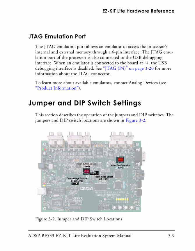
Jumper and DIP Switch SettingsThis section describes the operation of the jumpers and DIP switches. The jumpers and DIP switch locations are shown in Figure 3-2.
Figure 3-2. Jumper and DIP Switch Locations
ADSP-BF533 EZ-KIT Lite Evaluation System Manual 3-9
Jumper and DIP Switch Settings
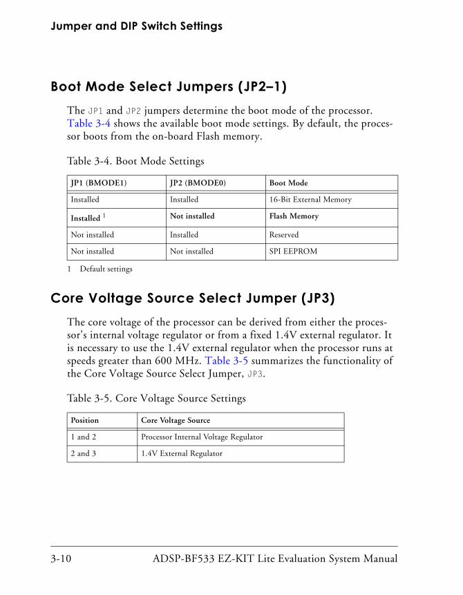
Boot Mode Select Jumpers (JP2–1)The JP1 and JP2 jumpers determine the boot mode of the processor. Table 3-4 shows the available boot mode settings. By default, the proces-sor boots from the on-board Flash memory.
Core Voltage Source Select Jumper (JP3)The core voltage of the processor can be derived from either the proces-sor’s internal voltage regulator or from a fixed 1.4V external regulator. It is necessary to use the 1.4V external regulator when the processor runs at speeds greater than 600 MHz. Table 3-5 summarizes the functionality of the Core Voltage Source Select Jumper, JP3.
Table 3-4. Boot Mode Settings
JP1 (BMODE1) JP2 (BMODE0) Boot Mode
Installed Installed 16-Bit External Memory
Installed 1
1 Default settings
Not installed Flash Memory
Not installed Installed Reserved
Not installed Not installed SPI EEPROM
Table 3-5. Core Voltage Source Settings
Position Core Voltage Source
1 and 2 Processor Internal Voltage Regulator
2 and 3 1.4V External Regulator
3-10 ADSP-BF533 EZ-KIT Lite Evaluation System Manual
EZ-KIT Lite Hardware Reference
Test DIP Switches (SW2–1)Two DIP switches (SW1 and SW2) are located on the bottom of the board. The switches are used only for testing and should always be in the “OFF” position.
Video Configuration Switch (SW3)The video configuration switch (SW3) controls how some video signals from the ADV7183 video decoder and ADV7171 video encoder are routed to the processor’s PPI. The switch also determines if the PF2 pin controls the OE of the ADV7183 video decoder outputs. Table 3-6 shows which processor’s signals are connected to the encoder and decoder when in the “ON” position.
Positions 1 thorough 5 of SW3 determine how and if the VSYNC, HSYNC, and FIELD control signals are routed to the processors PPI. In standard config-uration of the encoder and decoder, this is not necessary because the processor is capable of reading the embedded control information, which is in the data stream.
Table 3-6. Video Configuration Switch (SW3)
Switch Position (Default) Processor Signal Video Signal
1 (OFF) TMR1 (HSYNC) HSYNC (ADV7171)
2 (OFF) TMR1 (HSYNC) HS (ADV7183)
3 (OFF) TMR2 (VSYNC) VS (ADV7183)
4 (OFF) TMR2 (VSYNC) VSYNC (ADV7171)
5 (OFF) PF3 (FIELD) FIELD (ADV7183)
6 (ON) PF2 ~OE (ADV7183)
ADSP-BF533 EZ-KIT Lite Evaluation System Manual 3-11

Jumper and DIP Switch Settings
Position 6 of SW3 determines whether PF2 is connected to the ~OE signal of the ADV7183. When the switch “OFF”, PF2 can be used for other opera-tions, and the decoder output enable is held “HIGH” with a pull-up resistor.
Push Button Enable Switch (SW9)The push button enable switch (SW9) positions 1 through 4 allow the user to disconnect the drivers associated with the push buttons from the PF pins of the processor. Positions 5 and 6 are used to connect the transmit and receive the frame syncs and clocks of SPORT0. This is important when the AD1836 video decoder and the processor are communicating in I2S mode. Table 3-7 shows which PF is driven when the switch is in the “ON” position.
Table 3-7. Push Button Enable Switch (SW9)
Switch Position Default Setting Pin # Signal (Side 1) Pin # Signal (Side 2)
1 ON 1 SW4 12 PF8
2 ON 2 SW5 11 PF9
3 ON 3 SW6 10 PF10
4 ON 4 SW7 9 PF11
5 OFF 5 TFS0 8 RFS0
6 OFF 6 RSCLK0 7 TSCLK0
3-12 ADSP-BF533 EZ-KIT Lite Evaluation System Manual
EZ-KIT Lite Hardware Reference
LEDs and Push ButtonsThis section describes the functionality of the LEDs and push buttons. Figure 3-3 shows the locations of the LEDs and push buttons.
Programmable Flag Push Buttons (SW7–4)Four push buttons, SW7–4, are provided for general-purpose user input. The buttons connect to the processor’s programmable flag pins PF11–8. The push buttons are active “HIGH” and, when pressed, send a High (1) to the processor. Refer to “Using LEDs and Push Buttons” on page 2-10 for more information on how to use the PFs when programming the proces-sor. The push button enable switch (SW9) is capable of disconnecting the
Figure 3-3. LED and Push Button Locations
ADSP-BF533 EZ-KIT Lite Evaluation System Manual 3-13
LEDs and Push Buttons
push buttons from the PF (refer to “Push Button Enable Switch (SW9)” on page 3-12 for more information). The programmable flag signals and their corresponding switches are shown in Table 3-8.
Reset Push Button (SW8)The RESET push button resets all of the ICs on the board. One exception is the USB interface chip (U34). The chip is not being reset when the push button is pressed after the USB cable has been plugged in and communi-cation has been correctly initialized with the PC. After USB communication has been initialized, the only way to reset the USB is by powering down the board.
Power LED (LED1)When LED1 is lit (green), it indicates that power is being properly supplied to the board.
Reset LEDs (LED3–2)When LED2 is lit, it indicates that the master reset of all the major ICs is active. When LED3 is lit, the USB interface chip (U34) is being reset. The USB chips only reset on power-up, or if USB communication has not been initialized.
Table 3-8. Programmable Flag Switches
DSP Programmable Flag Pin Push Button Reference Designator
PF8 SW4
PF9 SW5
PF10 SW6
PF11 SW7
3-14 ADSP-BF533 EZ-KIT Lite Evaluation System Manual
EZ-KIT Lite Hardware Reference
User LEDs (LED9–4)Six LEDs are connected to six of the Flash memory (U5) general-purpose IO pins. The LEDs are active “HIGH” and are lit by writing a “1” to the correct memory address in the Flash memory. Refer to “Using LEDs and Push Buttons” on page 2-10 for more information about how to use the flash when programming the LEDs.
USB Monitor LED (LED11)The USB Monitor LED (LED11) indicates that USB communication has been initialized successfully and you may connect to the processor using a VisualDSP++ EZ-KIT Lite session. This should take approximately 15 seconds. If the LED does not light, try cycling power on the board and/or reinstalling the USB driver (see “Installing EZ-KIT Lite USB Driver” on page 1-7).
Table 3-9. User LEDs
LED Reference Designator Flash Port Name
LED4 PB0
LED5 PB1
LED6 PB2
LED7 PB3
LED8 PB4
LED9 PB5
ADSP-BF533 EZ-KIT Lite Evaluation System Manual 3-15
Connectors
ConnectorsThis section describes the connector functionality and provides informa-tion about mating connectors. The locations of the connectors are shown in Figure 3-4 on page 3-16.
Expansion Interface (J3–1)Three board-to-board connector footprints provide signals for most of the processor’s peripheral interfaces. The connectors are located at the bottom of the board. For more information about the expansion interface, see on page 3-8. For the availability and pricing of the J1, J2, and J3 connec-tors, contact Samtec.
Figure 3-4. Connector Locations
3-16 ADSP-BF533 EZ-KIT Lite Evaluation System Manual

EZ-KIT Lite Hardware Reference
Audio (J5–4)
Video (J8)
Power (J9)The power connector provides all of the power necessary to operate the EZ-KIT Lite board. The power connector supplies DC power to the board. The following table shows the power connector pinout.
Part Description Manufacturer Part Number
90 Position 0.05" Spacing, SMT (J1, J2, J3)
Samtec SFC-145-T2-F-D-A
Mating Connector
90 Position 0.05” Spacing (Through Hole)
Samtec TFM-145-x1 Series
90 Position 0.05” Spacing (Surface Mount)
Samtec TFM-145-x2 Series
90 Position 0.05” Spacing (Low Cost)
Samtec TFC-145 Series
Part Description Manufacturer Part Number
2x2 RCA Jacks (J5) SWITCHCRAFT PJRAS2X2S01
3x2 RCA Jacks (J4) SWITCHCRAFT PJRAS3X2S01
Mating Connector
Two channel RCA interconnect cable
Monster Cable BI100-1M
Part Description Manufacturer Part Number
3x2 RCA Jacks (J4) SWITCHCRAFT PJRAS3X2S01
ADSP-BF533 EZ-KIT Lite Evaluation System Manual 3-17
Connectors
The power connector supplies DC power to the EZ-KIT Lite board. Table 3-10 shows the power supply specifications.
FlashLINK (P1)The FlashLINK connector allows you to configure and program the STMicroelectronics DSM2150 flash/PLD chip. See “Configuring Flash Memory” on page 2-9 for more information about the FlashLINK connector.
Part Description Manufacturer Part Number
2.5 mm Power Jack (J9) SWITCHCRAFT RAPC712
Digi-Key SC1152-ND
Mating Power Supply (shipped with EZ-KIT Lite)
7.5V Power Supply GlobTek TR9CC2000LCP-Y
Table 3-10. Power Supply Specification
Terminal Connection
Center pin +7.5 VDC@2amps
Outer Ring GND
Part Description Manufacturer Part Number
Right-angle 7X2 Shrouded 0.1 spacing (J10)
TYCO 2-767004-2
Mating Assembly
FlashLINK JTAG Programmer ST Micro FL-101B
3-18 ADSP-BF533 EZ-KIT Lite Evaluation System Manual

EZ-KIT Lite Hardware Reference
RS232 (P2)The RS232-compatible connector is described in Table 3-11.
SPORT0 (P3)The SPORT0 connector is linked to a 20-pin connector. The connector’s pinout can be found in “Schematics” on page B-1. For pricing and avail-ability on these connectors, contact AMP.
Table 3-11. RS232 Connector
Part Description Manufacturer Part Number
DB9, Male, Right Angle (P2) Digi-Key A2096-ND
Mating Assembly
2m Female to female cable Digi-Key AE1016-ND
Part Description Manufacturer Part Number
20 position AMPMODU system 50 receptacle (P3)
AMP 104069-1
Mating Connectors
20 position ribbon cable connec-tor
AMP 111196-4
20 position AMPMODU system 20 connector
AMP 2-487937-0
20 position AMPMODU system 20 connector (w/o lock)
AMP 2-487938-0
Flexible film contacts (20 per connector)
AMP 487547-1
ADSP-BF533 EZ-KIT Lite Evaluation System Manual 3-19
Connectors
JTAG (P4)The JTAG header is the connecting point for a JTAG in-circuit emulator pod. When an emulator is connected to the JTAG header, the USB debug interface is disabled.
Pin 3 is missing to provide keying. Pin 3 in the mating connector should have a plug.
When using an emulator with the EZ-KIT Lite board, follow the connection instructions provided with the emulator.
3-20 ADSP-BF533 EZ-KIT Lite Evaluation System Manual
A BILL OF MATERIALS
er
Ref
eren
ce
Qua
ntit
y
Des
crip
tion
Ref
eren
ce
Des
ign
Man
ufac
tur
Par
t N
umbe
r
1 2 74LVC14A SOIC14 HEX-INVER-SCHMITT-TRIGGER
U10,U41 TI 74LVC14AD
2 1 IDT74FCT3244APY SSOP20 3.3V-OCTAL-BUFFER
U31 IDT IDT74FCT3244APY
3 1 IDT74FCT3807AQ QSOP203.3V 1-10 CLOCK DRIVER
U4 IDT IDT74FCT3807AQ
4 1 CY7C64603-128 PQFP128USB-TX/RX MICROCON-TROLLER
U34 CYPRESS CY7C64603-128NC
5 1 MMBT4401 SOT-23NPN TRANSISTOR 200MA
Q1 FAIRCHILD MMBT4401
6 1 74LVC00AD SOIC14 U9 PHILIPS 74LVC00AD
7 1 CY7C1019BV33-15VC SOJ32128K X 8 SRAM
U39 CYPRESS CY7C1019BV33-12VC
8 1 SN74AHC1G02 SOT23-5SINGLE-2 INPUT-NOR
U44 TI SN74AHC1G02DBVR
9 1 SN74LV164A SOIC148-BIT-PARALLEL-SERIAL
U35 TI SN74LV164AD
ADSP-BF533 EZ-KIT Lite Evaluation System Manual A-1
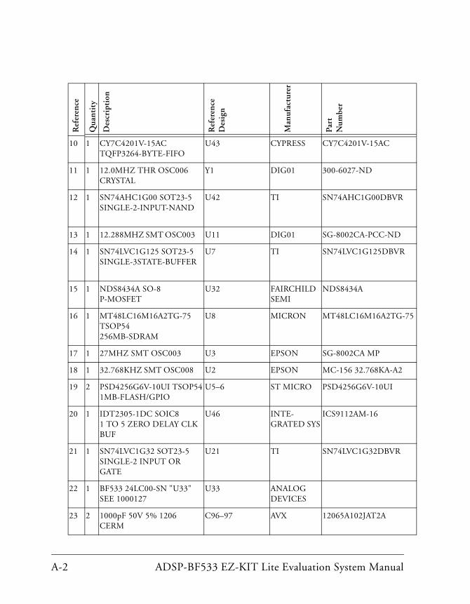
10 1 CY7C4201V-15AC TQFP3264-BYTE-FIFO
U43 CYPRESS CY7C4201V-15AC
11 1 12.0MHZ THR OSC006CRYSTAL
Y1 DIG01 300-6027-ND
12 1 SN74AHC1G00 SOT23-5SINGLE-2-INPUT-NAND
U42 TI SN74AHC1G00DBVR
13 1 12.288MHZ SMT OSC003 U11 DIG01 SG-8002CA-PCC-ND
14 1 SN74LVC1G125 SOT23-5 SINGLE-3STATE-BUFFER
U7 TI SN74LVC1G125DBVR
15 1 NDS8434A SO-8P-MOSFET
U32 FAIRCHILD SEMI
NDS8434A
16 1 MT48LC16M16A2TG-75 TSOP54256MB-SDRAM
U8 MICRON MT48LC16M16A2TG-75
17 1 27MHZ SMT OSC003 U3 EPSON SG-8002CA MP
18 1 32.768KHZ SMT OSC008 U2 EPSON MC-156 32.768KA-A2
19 2 PSD4256G6V-10UI TSOP541MB-FLASH/GPIO
U5–6 ST MICRO PSD4256G6V-10UI
20 1 IDT2305-1DC SOIC81 TO 5 ZERO DELAY CLK BUF
U46 INTE-GRATED SYS
ICS9112AM-16
21 1 SN74LVC1G32 SOT23-5SINGLE-2 INPUT OR GATE
U21 TI SN74LVC1G32DBVR
22 1 BF533 24LC00-SN "U33"SEE 1000127
U33 ANALOG DEVICES
23 2 1000pF 50V 5% 1206CERM
C96–97 AVX 12065A102JAT2A
Ref
eren
ce
Qua
ntit
y
Des
crip
tion
Ref
eren
ce
Des
ign
Man
ufac
ture
r
Par
t N
umbe
r
A-2 ADSP-BF533 EZ-KIT Lite Evaluation System Manual
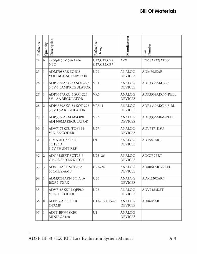
Bill Of Materials
24 6 2200pF 50V 5% 1206NPO
C12,C17,C22,C27,C32,C37
AVX 12065A222JAT050
25 1 ADM708SAR SOIC8VOLTAGE-SUPERVISOR
U29 ANALOG DEVICES
ADM708SAR
26 1 ADP3338AKC-33 SOT-2233.3V-1.0AMP REGULATOR
VR1 ANALOG DEVICES
ADP3338AKC-3.3
27 1 ADP3339AKC-5 SOT-2235V-1.5A REGULATOR
VR5 ANALOG DEVICES
ADP3339AKC-5-REEL
28 2 ADP3339AKC-33 SOT-2233.3V 1.5A REGULATOR
VR3–4 ANALOG DEVICES
ADP3339AKC-3.3-RL
29 1 ADP3336ARM MSOP8ADJ 500MA REGULATOR
VR6 ANALOG DEVICES
ADP3336ARM-REEL
30 1 ADV7171KSU TQFP44VID-ENCODER
U27 ANALOG DEVICES
ADV7171KSU
31 1 10MA AD1580BRT SOT23D1.2V-SHUNT-REF
D1 ANALOG DEVICES
AD1580BRT
32 2 ADG752BRT SOT23-6 CMOS-SPDT-SWITCH
U25–26 ANALOG DEVICES
ADG752BRT
33 3 AD8061ART SOT23-5300MHZ-AMP
U22–24 ANALOG DEVICES
AD8061ART-REEL
34 1 ADM3202ARN SOIC16RS232-TXRX
U30 ANALOG DEVICES
ADM3202ARN
35 1 ADV7183KST LQFP80VID-DECODER
U28 ANALOG DEVICES
ADV7183KST
36 8 AD8606AR SOIC8OPAMP
U12–13,U15–20 ANALOG DEVICES
AD8606AR
37 1 ADSP-BF533SKBC MINIBGA160
U1 ANALOG DEVICES
Ref
eren
ce
Qua
ntit
y
Des
crip
tion
Ref
eren
ce
Des
ign
Man
ufac
ture
r
Par
t N
umbe
r
ADSP-BF533 EZ-KIT Lite Evaluation System Manual A-3
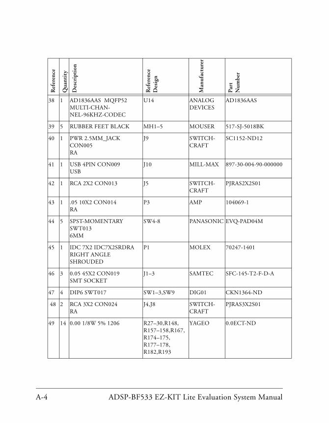
38 1 AD1836AAS MQFP52MULTI-CHAN-NEL-96KHZ-CODEC
U14 ANALOG DEVICES
AD1836AAS
39 5 RUBBER FEET BLACK MH1–5 MOUSER 517-SJ-5018BK
40 1 PWR 2.5MM_JACK CON005RA
J9 SWITCH-CRAFT
SC1152-ND12
41 1 USB 4PIN CON009 USB
J10 MILL-MAX 897-30-004-90-000000
42 1 RCA 2X2 CON013 J5 SWITCH-CRAFT
PJRAS2X2S01
43 1 .05 10X2 CON014 RA
P3 AMP 104069-1
44 5 SPST-MOMENTARY SWT013 6MM
SW4-8 PANASONIC EVQ-PAD04M
45 1 IDC 7X2 IDC7X2SRDRARIGHT ANGLE SHROUDED
P1 MOLEX 70247-1401
46 3 0.05 45X2 CON019SMT SOCKET
J1–3 SAMTEC SFC-145-T2-F-D-A
47 4 DIP6 SWT017 SW1–3,SW9 DIG01 CKN1364-ND
48 2 RCA 3X2 CON024 RA
J4,J8 SWITCH-CRAFT
PJRAS3X2S01
49 14 0.00 1/8W 5% 1206 R27–30,R148,R157–158,R167, R174–175,R177–178, R182,R193
YAGEO 0.0ECT-ND
Ref
eren
ce
Qua
ntit
y
Des
crip
tion
Ref
eren
ce
Des
ign
Man
ufac
ture
r
Par
t N
umbe
r
A-4 ADSP-BF533 EZ-KIT Lite Evaluation System Manual
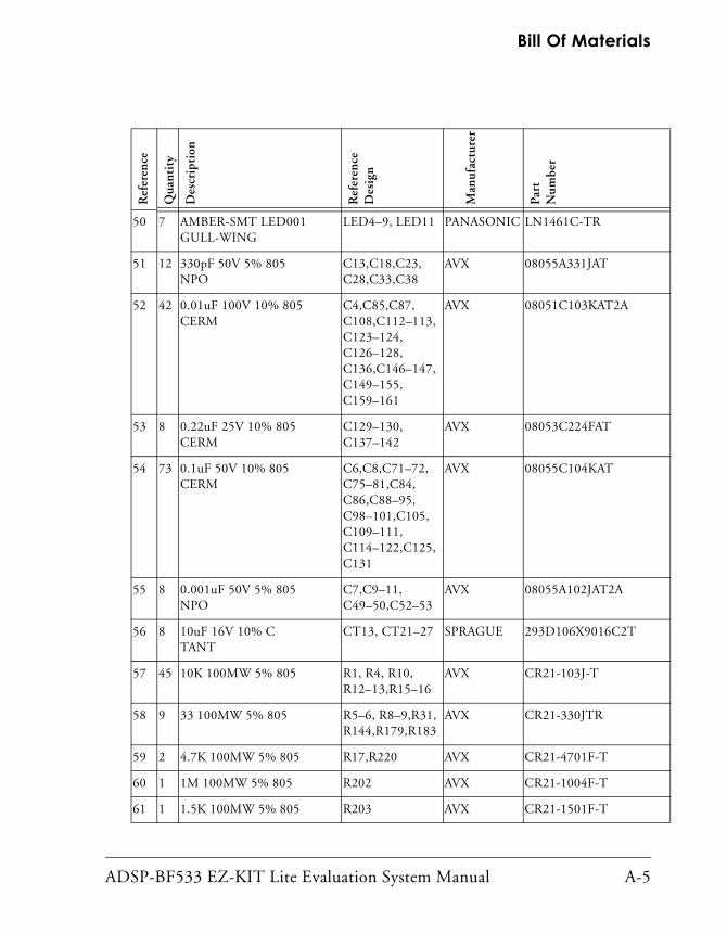
Bill Of Materials
50 7 AMBER-SMT LED001GULL-WING
LED4–9, LED11 PANASONIC LN1461C-TR
51 12 330pF 50V 5% 805NPO
C13,C18,C23,C28,C33,C38
AVX 08055A331JAT
52 42 0.01uF 100V 10% 805CERM
C4,C85,C87,C108,C112–113,C123–124,C126–128,C136,C146–147,C149–155,C159–161
AVX 08051C103KAT2A
53 8 0.22uF 25V 10% 805CERM
C129–130,C137–142
AVX 08053C224FAT
54 73 0.1uF 50V 10% 805CERM
C6,C8,C71–72,C75–81,C84,C86,C88–95,C98–101,C105,C109–111,C114–122,C125,C131
AVX 08055C104KAT
55 8 0.001uF 50V 5% 805NPO
C7,C9–11,C49–50,C52–53
AVX 08055A102JAT2A
56 8 10uF 16V 10% CTANT
CT13, CT21–27 SPRAGUE 293D106X9016C2T
57 45 10K 100MW 5% 805 R1, R4, R10, R12–13,R15–16
AVX CR21-103J-T
58 9 33 100MW 5% 805 R5–6, R8–9,R31,R144,R179,R183
AVX CR21-330JTR
59 2 4.7K 100MW 5% 805 R17,R220 AVX CR21-4701F-T
60 1 1M 100MW 5% 805 R202 AVX CR21-1004F-T
61 1 1.5K 100MW 5% 805 R203 AVX CR21-1501F-T
Ref
eren
ce
Qua
ntit
y
Des
crip
tion
Ref
eren
ce
Des
ign
Man
ufac
ture
r
Par
t N
umbe
r
ADSP-BF533 EZ-KIT Lite Evaluation System Manual A-5
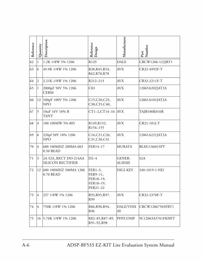
62 1 1.2K 1/8W 5% 1206 R129 DALE CRCW1206-122JRT1
63 6 49.9K 1/8W 1% 1206 R38,R45,R54,R62,R70,R78
AVX CR32-4992F-T
64 2 2.21K 1/8W 1% 1206 R212–213 AVX CR32-2211F-T
65 1 2000pF 50V 5% 1206CERM
C83 AVX 12065A202JAT2A
66 12 100pF 100V 5% 1206 NPO
C15,C20,C25,C30,C35,C40,
AVX 12061A101JAT2A
67 5 10uF 16V 10% B TANT
CT1–2,CT14–16 AVX TAJB106K016R
68 4 100 100MW 5% 805 R149,R152,R154–155
AVX CR21-101J-T
69 6 220pf 50V 10% 1206NPO
C16,C21,C26,C31,C36,C41
AVX 12061A221JAT2A
70 4 600 100MHZ 200MA 6030.50 BEAD
FER14–17 MURATA BLM11A601SPT
71 3 2A S2A_RECT DO-214AA SILICON RECTIFIER
D2–4 GENER-ALSEMI
S2A
72 12 600 100MHZ 500MA 12060.70 BEAD
FER1–5,FER9–11,FER18–19,FER18–19, FER21–22
DIGI-KEY 240-1019-1-ND
73 4 237 1/8W 1% 1206 R93,R95,R97,R99
AVX CR32-2370F-T
74 4 750K 1/8W 1% 1206 R86,R90,R94,R96
DALE/VISHAY
CRCW12067503FRT1
75 16 5.76K 1/8W 1% 1206 R82–85,R87–89,R91–92,R98
PHYCOMP 9C12063A5761FKHFT
Ref
eren
ce
Qua
ntit
y
Des
crip
tion
Ref
eren
ce
Des
ign
Man
ufac
ture
r
Par
t N
umbe
r
A-6 ADSP-BF533 EZ-KIT Lite Evaluation System Manual
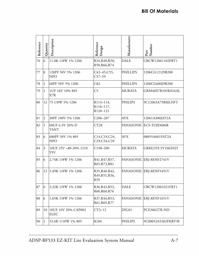
Bill Of Materials
76 6 11.0K 1/8W 1% 1206 R34,R48,R50,R58,R66,R74
DALE CRCW12061102FRT1
77 8 120PF 50V 5% 1206 NPO
C42–45,C55,C57–59
PHILLIPS 1206CG121J9B200
78 1 68PF 50V 5% 1206 C82 PHILLIPS 1206CG680J9B200
79 1 1UF 16V 10% 805X7R
C5 MURATA GRM40X7R105K016AL
80 12 75 1/8W 5% 1206 R113–114,R116–117,R120–121
PHILIPS 9C12063A75R0JLHFT
81 2 30PF 100V 5% 1206 C206–207 AVX 12061A300JAT2A
82 1 68UF 6.3V 20% DTANT
CT28 PANASONIC ECS-TOJD686R
83 6 680PF 50V 1% 805 NPO
C14,C19,C24,C29,C34,C39
AVX 08055A681FAT2A
84 3 10UF 25V +80-20% 1210Y5V
C198–200 MURATA GRM235Y.5V106Z025
85 6 2.74K 1/8W 1% 1206 R41,R47,R57,R65,R73,R81
PANASONIC ERJ-8ENF2741V
86 12 5.49K 1/8W 1% 1206 R35,R40,R42,R49,R51,R56,R59
PANASONIC ERJ-8ENF5491V
87 6 3.32K 1/8W 1% 1206 R36,R43,R52,R60,R68,R76
DALE CRCW12063321FRT1
88 6 1.65K 1/8W 1% 1206 R37,R44,R53,R61,R69,R77
PANASONIC ERJ-8ENF1651V
89 10 10UF 16V 20% CAP002ELEC
CT3–12 DIG01 PCE3062TR-ND
90 1 53.6K 1/10W 1% 805 R184 PHILIPS 9C08052A5362FKRT/R
Ref
eren
ce
Qua
ntit
y
Des
crip
tion
Ref
eren
ce
Des
ign
Man
ufac
ture
r
Par
t N
umbe
r
ADSP-BF533 EZ-KIT Lite Evaluation System Manual A-7

91 1 10UH 47 +/-20 IND001 L12 DIG01 445-1202-2-ND
92 2 10K 50MW 5% BGA36 RN1–2 CTS RT130B7
93 15 0.00 100MW 5% 805 R3,R22,R24–25,R111,R132,R135–136,R141,R186–189,R210,R222
VISHAY CRCW0805 0.0 RT1
94 1 190 100MHZ 5A FER002 FER23 MURATA DLW5BSN191SQ2
95 1 3.32K 100MW 1% 805 C188 DIG01 P3.32KCCTR-ND
96 3 22 1/10W 5% 805 R14, R180–181 VISHAY/DALE
CRCW0805220JRT1
97 6 0.68UH 0.72 10% 805 L4–9 MURATA LQG21NR68K10T1
98 1 1A ZHCS1000 SOT23D SCHOTTKY
D5 ZETEX ZHCS1000
99 1 5.6K 1/10W 5% 805 R140 VISHAY CRCW0805562JRT1
100 3 2.2UH 0.63 10% 805 L1–3 MURATA LQG21N2R2K10
101 3 1UF 10V 10% 805 C60–61,C104 AVX 0805ZC105KAT2A
102 2 18PF 50VDC 5% 805CERM
C1, C3 PANASONIC ECJ-2VC1H180J
103 1 10M 1/8W 5% 805 R20 AVX CR21-106J-T
104 1 DB9 9PIN DB9MRIGHT ANGLE MALE
P2 3M 787203-2
105 7 1K 1/8W 5% 1206 R115,R118–119,R125–126,R131
AVX CR32-102J-T
106 3 100K 1/8W 5% 1206 R112,R130,R176 CR1206-1003FRT1
107 2 22 1/8W 5% 1206 R200,R207 DALE CRCW1206220JRT1
Ref
eren
ce
Qua
ntit
y
Des
crip
tion
Ref
eren
ce
Des
ign
Man
ufac
ture
r
Par
t N
umbe
r
A-8 ADSP-BF533 EZ-KIT Lite Evaluation System Manual
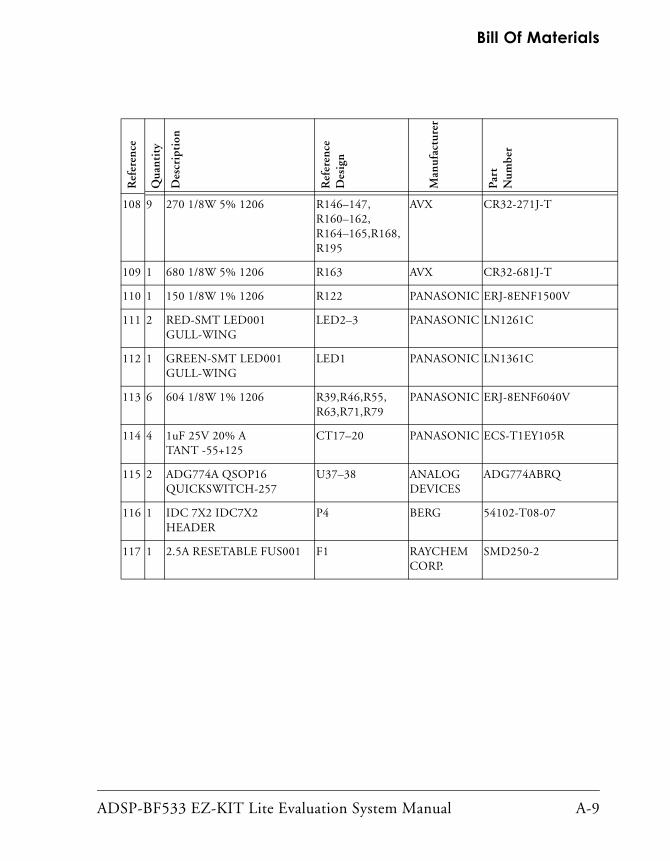
Bill Of Materials
108 9 270 1/8W 5% 1206 R146–147,R160–162,R164–165,R168,R195
AVX CR32-271J-T
109 1 680 1/8W 5% 1206 R163 AVX CR32-681J-T
110 1 150 1/8W 1% 1206 R122 PANASONIC ERJ-8ENF1500V
111 2 RED-SMT LED001GULL-WING
LED2–3 PANASONIC LN1261C
112 1 GREEN-SMT LED001GULL-WING
LED1 PANASONIC LN1361C
113 6 604 1/8W 1% 1206 R39,R46,R55,R63,R71,R79
PANASONIC ERJ-8ENF6040V
114 4 1uF 25V 20% ATANT -55+125
CT17–20 PANASONIC ECS-T1EY105R
115 2 ADG774A QSOP16QUICKSWITCH-257
U37–38 ANALOG DEVICES
ADG774ABRQ
116 1 IDC 7X2 IDC7X2HEADER
P4 BERG 54102-T08-07
117 1 2.5A RESETABLE FUS001 F1 RAYCHEM CORP.
SMD250-2
Ref
eren
ce
Qua
ntit
y
Des
crip
tion
Ref
eren
ce
Des
ign
Man
ufac
ture
r
Par
t N
umbe
r
ADSP-BF533 EZ-KIT Lite Evaluation System Manual A-9

A-10 ADSP-BF533 EZ-KIT Lite Evaluation System Manual
A0167-2001 1.6
4
3
2
1
A B C D
Nashua, NH 03063
A B C D
4
3
2
1
PH: 1-800-ANALOGD
C
Approvals Date
Drawn
Checked
Engineering Date
Size
Title
Board No. Rev
Sheet of
DEVICESANALOG 20 Cotton Road
DNP = Do Not Populate
ADSP-BF533 EZ-KIT Lite
ADSP-BF533 EZ-KIT LITE - TITLE
1313-24-2003_13:34
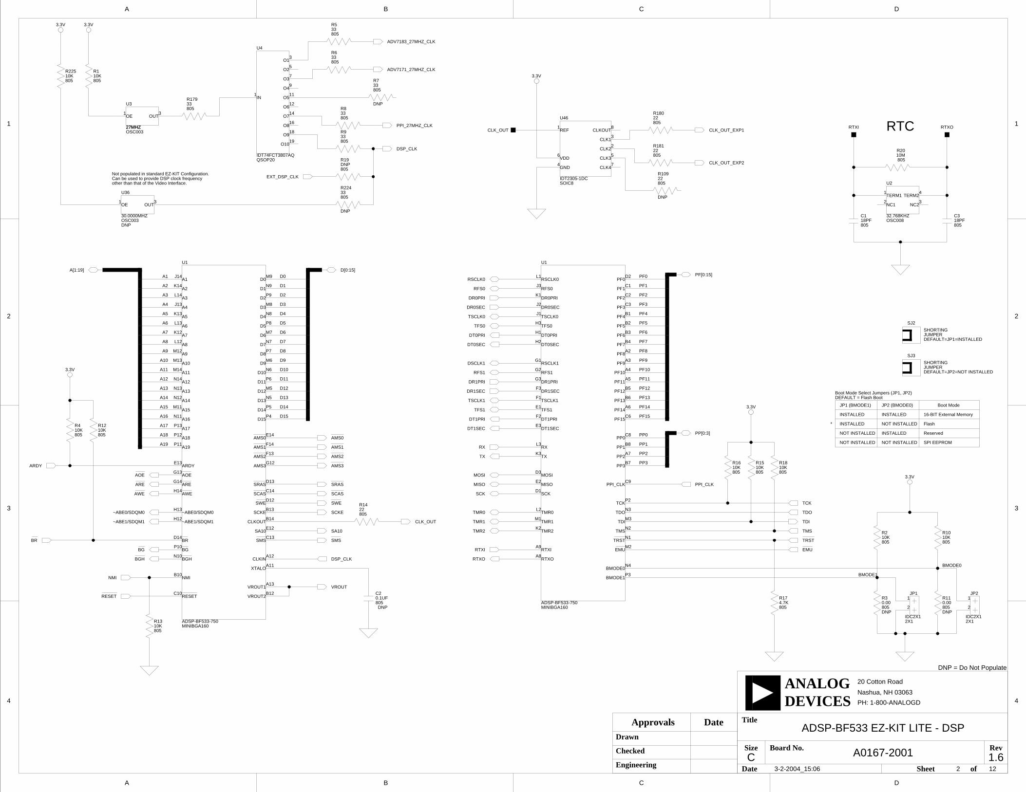
3.3V
3.3V
3.3V
3.3V
3.3V
IN
O1
O10
O2
O3
O4
O5
O6
O7
O8
O9
NC1 NC2
TERM1 TERM2
CLK2
CLK1
GND
CLK3VDD
CLK4
CLKOUTREF
3.3V
A0167-2001 1.6
4
3
2
1
A B C D
Nashua, NH 03063
A B C D
4
3
2
1
PH: 1-800-ANALOGD
C
Approvals Date
Drawn
Checked
Engineering Date
Size
Title
Board No. Rev
Sheet of
DEVICESANALOG 20 Cotton Road
DNP = Do Not Populate
OE OUT
OE OUT
A1
A10
A11
A12
A13
A14
A15
A16
A17
A18
A19
A2
A3
A4
A5
A6
A7
A8
A9
AMS3ARDY
CLKIN
CLKOUT
D0
D1
D10
D11
D12
D13
D14
D15
D2
D3
D4
D5
D6
D7
D8
D9
NMI
SA10
SCKE
VROUT1
VROUT2
XTALO
~ABE0/SDQM0
~ABE1/SDQM1
AMS0
AMS1
AMS2
AOE
ARE
AWE
BG
BGH
BR
RESET
SCAS
SMS
SRAS
SWE
BMODE0
BMODE1
DR0PRI
DR0SEC
DR1PRI
DR1SEC
DT0PRI
DT0SEC
DT1PRI
DT1SEC
PF0
PF1
PF10
PF11
PF12
PF13
PF14
PF15
PF2
PF3
PF4
PF5
PF6
PF7
PF8
PF9
PP0
PP1
PP2
PP3
PPI_CLK
RFS0
RFS1
RSCLK0
RSCLK1
RTXI
RTXO
RX
SCK
TCK
TDI
TDO
TFS0
TFS1
TMR0
TMR1
TMR2 TMS
TSCLK0
TSCLK1
TX
EMU
TRST
MOSI
MISO
JUMPERSHORTING
JUMPERSHORTING
NOT INSTALLED
INSTALLED
RTC
Can be used to provide DSP clock frequencyother than that of the Video Interface.
Not populated in standard EZ-KIT Configuration.
INSTALLED INSTALLED
NOT INSTALLED
NOT INSTALLED
NOT INSTALLED
Flash
Reserved
SPI EEPROM
Boot Mode Select Jumpers (JP1, JP2)
JP1 (BMODE1) JP2 (BMODE0)
16-BIT External Memory
Boot Mode
DEFAULT = Flash Boot
INSTALLED*
DEFAULT=JP1=INSTALLED
SJ2
SJ3
DEFAULT=JP2=NOT INSTALLED
1223-2-2004_15:06
N4
P3
K1
J2
G3
F3
H1
H2
F2
E3
D2
C1
A4
A5
B5
B6
A6
C6
C2
C3
B1
B2
B3
B4
A2
A3
C8
B8
A7
B7
C9
J3
G2
L1
G1
A9
A8
L3
D1
P2
M3
N3
H3
E1
L2
M1
K2 N2
J1
F1
K3
M2
N1
D3
E2
U1
MINIBGA160ADSP-BF533-750
J14
M13
M14
N14
N13
N12
M11
N11
P13
P12
P11
K14
L14
J13
K13
L13
K12
L12
M12
E13
A12
B14
M9
N9
N6
P6
M5
N5
P5
P4
P9
M8
N8
P8
M7
N7
P7
M6
B10
E12
B13
A13
A11
H13
H12
E14
F14
F13
G12
G13
G14
H14
P10
N10
D14
C10
C14
C13
D13
D12
B12
U1
ADSP-BF533-750MINIBGA160
2
1
2X1IDC2X1
JP1
BMODE1
BMODE0
R3
8050.00
DNP
1
2
JP2
IDC2X12X1
1 3
U3
OSC00327MHZ27MHZ
31
DNP
30.0000MHZOSC003
U36R224
DNP
33805
DSP_CLK
R22510K805
EXT_DSP_CLK
R19DNP805
80533R179
R2
80510K
ADSP-BF533 EZ-KIT LITE - DSP
2
3
4
56
7
81
IDT2305-1DCSOIC8
U46
2
1
3
4
U2
OSC00832.768KHZ
1
3
19
5
7
9
11
12
14
16
18
U4
QSOP20IDT74FCT3807AQ
R18022805
CLK_OUT_EXP1
CLK_OUT_EXP2
80522R181
R109
DNP
22805
CLK_OUT
CLK_OUT
80522R14
R7
DNP
33805
80533R8
C3
80518PF
C1
80518PF
R2010M805
R533805
PPI_27MHZ_CLK
ADV7183_27MHZ_CLK
ADV7171_27MHZ_CLK
D0
D1
D2
D3
D4
D5
D6
D7
D8
D9
D10
D11
D12
D13
D14
D[0:15]
D15
A11
A10
A8
A9
A12
A4
A1
A19
A17
A15
A[1:19]
A5
A2
A3
A6
A7
A13
A14
A16
A18
BG
NMI
RESET
VROUT
DSP_CLK
RTXORTXI
10K805
R10
DNP
0.00805
R11
10K805
R1810K805
R15
4.7K805
R17
R16
80510K
PPI_CLK
TSCLK1
DSCLK1
TSCLK0
RSCLK0
TDO
TDI
R4
80510K
ARDY
R933805
C2
8050.1UF
DNP
DR1SEC
TRST
TMS
PP1
PP[0:3]
PP3
PP2
PP0
TCK
10K805
R12
80533R6
PF[0:15]PF0
PF1
PF2
PF3
PF4
PF5
PF6
PF7
PF8
PF9
PF10
PF11
PF12
PF13
PF14
PF15
80510KR1
RTXO
RTXI
TMR0
TMR1
TMR2
MOSI
MISO
SCK
TX
RX
EMU
RFS1
DR1PRI
TFS1
DT1PRI
DT1SEC
RFS0
DR0PRI
TFS0
DT0PRI
DT0SEC
DR0SEC
10K805
R13
AMS0
AMS1
AMS2
AMS3
BGH
BR
~ABE1/SDQM1
~ABE0/SDQM0
AWE
ARE
AOE
SRAS
SCAS
SWE
SCKE
SA10
SMS
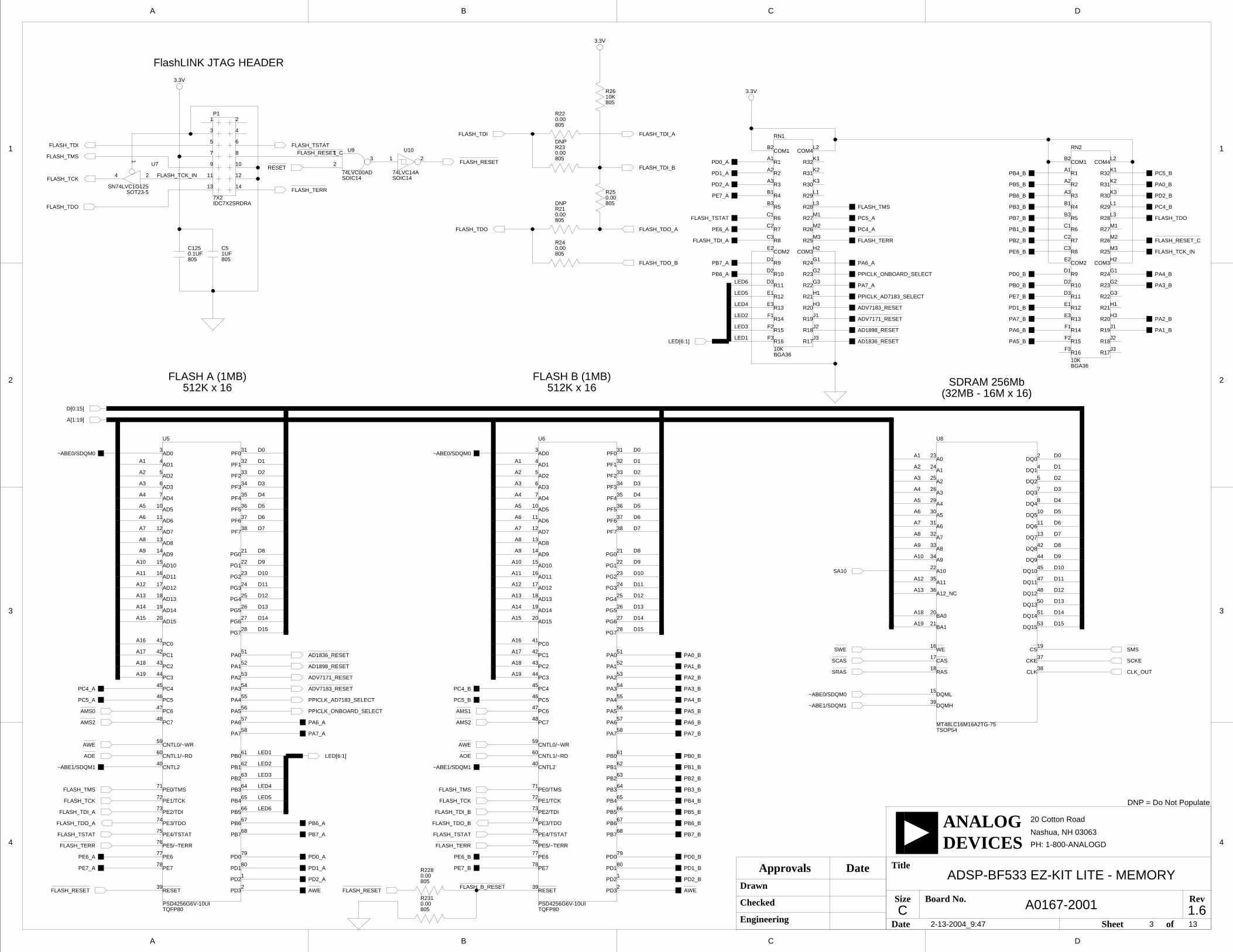
3.3V
A0167-2001 1.6
4
3
2
1
A B C D
Nashua, NH 03063
A B C D
4
3
2
1
PH: 1-800-ANALOGD
C
Approvals Date
Drawn
Checked
Engineering Date
Size
Title
Board No. Rev
Sheet of
DEVICESANALOG 20 Cotton Road
DNP = Do Not Populate
3.3V
COM2
R16
R15
R14
R13
R12
R10
R24
R23
R22
R21
R20
R19
R27
R28
R29
R30
R31
R32
R2
R3
R4
R5
R6
R7
R8
R26
R1
R18
COM1
R9
R11
COM4
R25
COM3
R17
3.3V
COM2
R16
R15
R14
R13
R12
R10
R24
R23
R22
R21
R20
R19
R27
R28
R29
R30
R31
R32
R2
R3
R4
R5
R6
R7
R8
R26
R1
R18
COM1
R9
R11
COM4
R25
COM3
R17
PE7
PE3/TDO
PE2/TDI
PE1/TCK
PE0/TMS
PB7
PB6
PB5
PB4
PB3
PB2
PB1
PB0CNTL1/~RD
CNTL0/~WR
PA7
PA6
PA5
PA4
PA3
PA2
PA1
PA0
PC7
PC6
PC5
PC4
PC3
PC0
CNTL2
PF7
PF6
PF4
PF5
PF3
PF2
PF1
PG7
PG6
PG5
PG4
PG3
PG2
PG1
PG0
AD15
AD14
AD13
AD12
AD11
AD10
AD9
AD8
AD7
AD6
AD5
AD4
AD3
AD2
AD1
AD0
PD3
PF0
PD1
PC2
PC1
RESET
PD2
PD0PE6
PE5/~TERR
PE4/TSTAT
A0
A1
A10
A11
A12_NC
A2
A3
A4
A5
A6
A7
A8
A9
CKE
CLK
DQ0
DQ1
DQ10
DQ11
DQ12
DQ13
DQ14
DQ15
DQ2
DQ3
DQ4
DQ5
DQ6
DQ7
DQ8
DQ9
DQMH
DQML
CAS
CS
RAS
WE
BA1
BA0
PE7
PE3/TDO
PE2/TDI
PE1/TCK
PE0/TMS
PB7
PB6
PB5
PB4
PB3
PB2
PB1
PB0CNTL1/~RD
CNTL0/~WR
PA7
PA6
PA5
PA4
PA3
PA2
PA1
PA0
PC7
PC6
PC5
PC4
PC3
PC0
CNTL2
PF7
PF6
PF4
PF5
PF3
PF2
PF1
PG7
PG6
PG5
PG4
PG3
PG2
PG1
PG0
AD15
AD14
AD13
AD12
AD11
AD10
AD9
AD8
AD7
AD6
AD5
AD4
AD3
AD2
AD1
AD0
PD3
PF0
PD1
PC2
PC1
RESET
PD2
PD0PE6
PE5/~TERR
PE4/TSTAT
512K x 16512K x 16FLASH A (1MB)
(32MB - 16M x 16)SDRAM 256MbFLASH B (1MB)
FlashLINK JTAG HEADER
2-13-2004_9:47 3 13
8050.00R231
FLASH_B_RESET
R2280.00805
75
76
77 79
1
39
42
43
80
31
2
3
4
5
6
7
10
11
12
13
14
15
16
17
18
19
20
21
22
23
24
25
26
27
28
32
33
34
36
35
37
38
40
41
44
45
46
47
48
51
52
53
54
55
56
57
58
59
60 61
62
63
64
65
66
67
68
71
72
73
74
78
PSD4256G6V-10UITQFP80
U6
PA1_B
~ABE0/SDQM0
RESET
32
1
74LVC00ADSOIC14
U9FLASH_RESET_C
1
3
5
7
9
11
13
2
4
6
8
10
12
14
IDC7X2SRDRA7X2
P1
23
24
22
35
36
25
26
29
30
31
32
33
34
37
38
2
4
45
47
48
50
51
53
5
7
8
10
11
13
42
44
39
15
17
19
18
16
21
20
U8
TSOP54MT48LC16M16A2TG-75
~ABE1/SDQM1
~ABE0/SDQM0
SRAS
SCAS
SWE
CLK_OUT
FLASH_RESET1 2
74LVC14ASOIC14
U10
FLASH_TSTAT
78
74
73
72
71
68
67
66
65
64
63
62
6160
59
58
57
56
55
54
53
52
51
48
47
46
45
44
41
40
38
37
35
36
34
33
32
28
27
26
25
24
23
22
21
20
19
18
17
16
15
14
13
12
11
10
7
6
5
4
3
2
31
80
43
42
39
1
7977
76
75
TQFP80PSD4256G6V-10UI
U5
1UF805
C5
SMS
SCKE
SA10
PA7_A
PA6_A
PPICLK_ONBOARD_SELECT
PPICLK_AD7183_SELECT
ADV7183_RESET
ADV7171_RESET
AD1898_RESET
AD1836_RESET
LED5
LED4
LED3
LED2
LED6
LED[6:1]LED1
LED2
LED5
LED4
LED3
LED1LED[6:1]
LED6
FLASH_TCK_IN
FLASH_RESET_C
FLASH_TDO
PA5_B
PA6_B
PA7_B
PD1_B
PE7_B
PD0_B
PE6_B
FLASH_TERR
FLASH_TMS
ADV7171_RESET
ADV7183_RESET
PE6_A
PE7_A
PD2_A
PD1_A
PD0_A
E2
F3
F2
F1
E3
E1
D2
G1
G2
G3
H1
H3
J1
M1
L3
L1
K3
K2
K1
A2
A3
B1
B3
C1
C2
C3
M2
A1
J2
B2
D1
D3
L2
M3
H2
J3
BGA3610K
RN1
PB7_A
PB6_A
24
1
SOT23-5SN74LVC1G125
U7FLASH_TMS
J3
H2
M3
L2
D3
D1
B2
J2
A1
M2
C3
C2
C1
B3
B1
A3
A2
K1
K2
K3
L1
L3
M1
J1
H3
H1
G3
G2
G1
D2
E1
E3
F1
F2
F3
E2
BGA3610K
RN2
8050.00
DNPR21
8050.00
DNPR23
8050.00R22
8050.00R25
8050.00R24
80510KR26
PE6_A
PE7_A
FLASH_TDO_A
FLASH_TDI FLASH_TSTAT
FLASH_TERR
FLASH_TCK_IN
FLASH_TDO
FLASH_TMS
FLASH_TCK
FLASH_TDI_A
PD0_A
PD1_A
PD2_A
AWE
PC4_A
PC5_A
AMS0
ADSP-BF533 EZ-KIT LITE - MEMORY
~ABE1/SDQM1
FLASH_RESET
FLASH_TERR
FLASH_TSTAT
FLASH_TDO_A
AOE
AWE
AMS2
FLASH_TDI
FLASH_TDO
FLASH_TDI_A
FLASH_TDO_B
FLASH_TCK
FLASH_TDI_B
FLASH_TDI_A
PB7_A
PB6_A
PA6_A
PPICLK_ONBOARD_SELECT
PA7_A
PPICLK_AD7183_SELECT
AD1898_RESET
AD1836_RESET
PC5_A
PC4_A
PB4_B
PB5_B
PB6_B
PB3_B
PB7_B
PB2_B
PB1_B
PB0_B
PA4_B
PA3_B
PA2_B
PC5_B
PD2_B
PA0_B
PC4_B
0.1UF805
C125
FLASH_RESET
PE7_B
PB7_B
PB6_B
PB5_B
PB4_B
PB3_B
PB2_B
PB1_B
PB0_B
PA7_B
PA6_B
PA5_B
PA4_B
PA3_B
PA2_B
PA1_B
PA0_B
PC5_B
PC4_B
~ABE1/SDQM1
~ABE0/SDQM0
AWE
PD1_B
PD2_B
PD0_BPE6_B
FLASH_TERR
FLASH_TSTAT
D12
D11
D10
D9
D8
D7
D6
D5
D4
D2
D1
D0D0
D1
D2
D4
D6
D11
D12
D13
D14
D15
D8
D7
D0
D1
D2
D3
D4
D5
D6
D9
D10
D11
D12
D13
D14
D15
D[0:15]
D8
D9
D7
D3D3
D5
D10
D14
D13
D15
FLASH_TDO_B
FLASH_TDI_B
FLASH_TCK
FLASH_TMS
AOE
AWE
AMS2
AMS1
A18
A19
A5
A9A10
A1A1
A2
A3
A4
A6
A7
A8
A10
A11
A12
A13
A14
A15
A16
A17
A18
A19
A2
A15
A16
A19
A18
A17
A14
A13
A12
A11
A10
A9
A8
A7
A6
A5
A4
A3
A[1:19]
A2
A3
A4
A5
A6
A7
A8
A9
A12
A13
A1
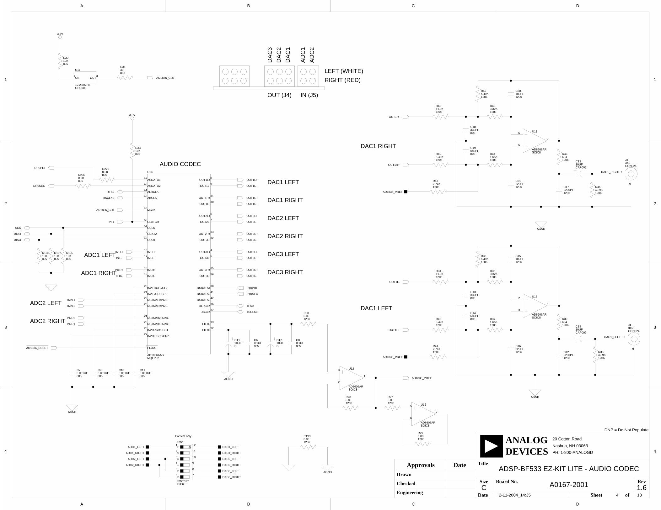
AGND
AGND
AGND
AGND
3.3V
A0167-2001 1.6
4
3
2
1
A B C D
Nashua, NH 03063
A B C D
4
3
2
1
PH: 1-800-ANALOGD
C
Approvals Date
Drawn
Checked
Engineering Date
Size
Title
Board No. Rev
Sheet of
DEVICESANALOG 20 Cotton Road
DNP = Do Not Populate
AGND
12
45
6
ON
3
OE OUT
3.3V
PD/RST
IN2R+/CR2/CR2
IN2R-/CR1/CR1
NC/IN2R1/IN2R+
NC/IN2R2/IN2R-
NC/IN2L2/IN2L-
NC/IN2L1/IN2L+
IN2L-/CL1/CL1
IN2L+/CL2/CL2
FILTD
FILTR
OUT3R-
OUT3R+
OUT3L-
OUT3L+
OUT2R-
OUT2R+
OUT2L-
OUT2L+
OUT1R-
OUT1R+
OUT1L-
OUT1L+
IN1R-
IN1R+
IN1L-
IN1L+
COUT
CDATA
CCLK
CLATCH
MCLK
DLRCLK
DBCLK
ASDATA1
ASDATA2
ALRCLK
ABCLK
DSDATA2
DSDATA1
DSDATA3
DAC1 LEFT
DAC1 LEFT
DAC1 RIGHT
DAC2 LEFT
DAC2 RIGHT
DAC3 LEFT
DAC3 RIGHT
ADC2 LEFT
ADC2 RIGHT
ADC1 LEFT
ADC1 RIGHT
AUDIO CODEC
For test only
DAC1 RIGHT
DA
C1
DA
C2
DA
C3
AD
C1
AD
C2
IN (J5)OUT (J4)
RIGHT (RED)
LEFT (WHITE)
2-11-2004_14:35 4 13
R2290.00805
8050.00R230
3
27
26
25
24
23
22
21
20
12
13
34
35
5
4
32
33
7
6
30
31
9
8
19
18
17
16
49
2
51
50
45
38
41
42
36
37
47
48
44
43
MQFP52AD1836AAS
U14
10K805
R33
RFS0
RSCLK0
PF4
TFS0
TSCLK0
R29
12060.00
12060.00R28
0.001206
R27
6
5
7
SOIC8AD8606AR
U12
1
3
2
AD8606ARSOIC8
U12
1
3
2
AD8606ARSOIC8
U13
R300.001206
DAC1_LEFT
CAP00210UFCT4
49.9K1206
R45
DAC1_RIGHT
CAP00210UFCT3
OUT3R+
DT0PRI
DT0SEC
OUT3R-
OUT3L-
OUT2R-
OUT2L-
OUT1L-
OUT1R+
OUT1R-
AD1836_VREF
12062.74KR41
1 3
OSC00312.288MHZ
U11
9
7
J4
CON0243X2
8
9
J4
CON0243X2
1
2
3
4
5
6 7
8
9
10
11
12
SWT017DIP6
SW1
AD1836_CLK
SCK
8050.001UFC7
0.1UF805
C810UFB
CT2
8050.1UFC6
B10UFCT1
ADC1_RIGHT
ADC1_LEFT
DAC2_LEFT
DAC3_LEFT
DAC3_RIGHT
DAC2_RIGHT
DAC1_RIGHT
DAC1_LEFT
33805
R31
AD1836_CLK
ADSP-BF533 EZ-KIT LITE - AUDIO CODEC
80510KR32
ADC2_LEFT
ADC2_RIGHT
0.001UF805
C9
8050.001UFC10
0.001UF805
C11
AD1836_RESET
IN2R1
IN2R2
IN2L2
IN2L1
OUT1L+
OUT1L-
OUT1R+
OUT1R-
OUT2L+
OUT2R+
OUT3L+
IN1R-
IN1R+
IN1L-
IN1L+
MISO
MOSI
7
5
6
AD8606ARSOIC8
U13
5.49K1206
R49
11.0K1206
R48
12062.74KR47
1206604R46
220PF1206
C21
1.65K1206
R44
100PF1206
C20
3.32K1206
R43
5.49K1206
R42
680PF805
C19
330PF805
C18
2200PF1206
C17
5.49K1206
R40
1206604R39
220PF1206
C16
1.65K1206
R37
100PF1206
C15
3.32K1206
R36
5.49K1206
R35
680PF805
C14
330PF805
C13
11.0K1206
R34
2200PF1206
C12
OUT1L+
AD1836_VREF
AD1836_VREF49.9K1206
R38
0.001206
R193
R106
80510K10K
805
R107R108
80510K
DR0SEC
DR0PRI
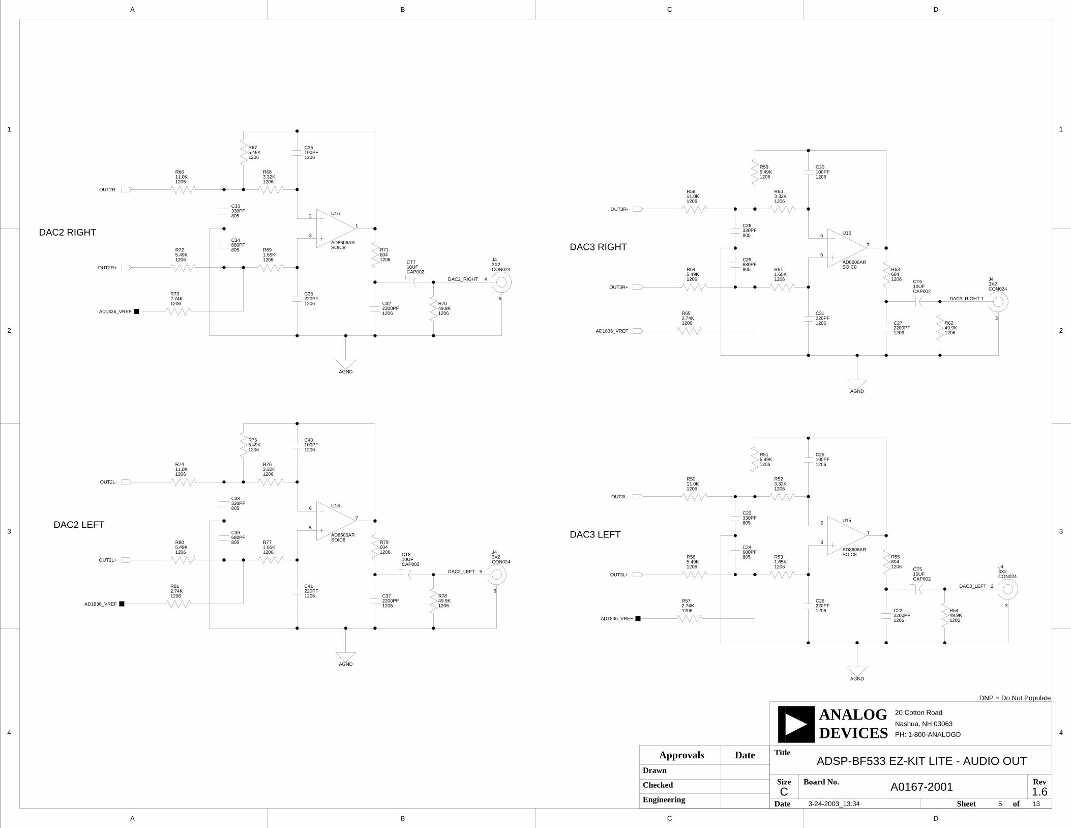
AGND
AGND
AGND
A0167-2001 1.6
4
3
2
1
A B C D
Nashua, NH 03063
A B C D
4
3
2
1
PH: 1-800-ANALOGD
C
Approvals Date
Drawn
Checked
Engineering Date
Size
Title
Board No. Rev
Sheet of
DEVICESANALOG 20 Cotton Road
DNP = Do Not Populate
AGND
DAC2 RIGHT
DAC3 RIGHT
DAC3 LEFTDAC2 LEFT
3-24-2003_13:34 5 13
ADSP-BF533 EZ-KIT LITE - AUDIO OUT
1
3
2
AD8606ARSOIC8
U15
49.9K1206
R62
DAC3_RIGHT
CAP00210UFCT6
DAC3_LEFT
49.9K1206
R54
CAP00210UFCT5
49.9K1206
R78
DAC2_LEFT
CAP00210UFCT8
49.9K1206
R70
DAC2_RIGHT
CAP00210UFCT7
OUT3R-
OUT3R+
2
3
J4
CON0243X2
1206604R63
2200PF1206
C27
7
5
6
AD8606ARSOIC8
U15
5.49K1206
R64
11.0K1206
R58
2200PF1206
C22
1206604R55
1.65K1206
R53
220PF1206
C26
100PF1206
C25
3.32K1206
R52
5.49K1206
R51
11.0K1206
R50
5.49K1206
R56
12062.74KR65
220PF1206
C31
1.65K1206
R61
100PF1206
C30
3.32K1206
R60
5.49K1206
R59
680PF805
C29
330PF805
C28
12062.74KR57
680PF805
C24
330PF805
C23
AD1836_VREF
AD1836_VREF
3
1
J4
CON0243X2
OUT3L-
OUT3L+
7
5
6
AD8606ARSOIC8
U16
12062.74KR81
5.49K1206
R80
1206604R79
220PF1206
C41
1.65K1206
R77
100PF1206
C40
3.32K1206
R76
5.49K1206
R75
680PF805
C39
330PF805
C38
11.0K1206
R74
2200PF1206
C37
5
6
J4
CON0243X2
1
3
2
AD8606ARSOIC8
U16
12062.74KR73
5.49K1206
R72
1206604R71
220PF1206
C36
1.65K1206
R69
100PF1206
C35
3.32K1206
R68
5.49K1206
R67
680PF805
C34
330PF805
C33
11.0K1206
R66
2200PF1206
C32
4
6
J4
CON0243X2
AD1836_VREF
OUT2L+
OUT2L-
OUT2R+
OUT2R-
AD1836_VREF
AGND
AGND
AGND
AGND
AGND
AGND
AGND
AGND
AGND
AGND
AGND
A0167-2001 1.6
4
3
2
1
A B C D
Nashua, NH 03063
A B C D
4
3
2
1
PH: 1-800-ANALOGD
C
Approvals Date
Drawn
Checked
Engineering Date
Size
Title
Board No. Rev
Sheet of
DEVICESANALOG 20 Cotton Road
DNP = Do Not Populate
AGND
AGND
AGND
ADC1 RIGHT
ADC1 LEFT
ADC2 RIGHT
ADC2 LEFT
1363-24-2003_13:34
6
5
7
AD8606AR
U17
SOIC8
7
5
6 U18
AD8606ARSOIC8
100PFC48
1206
C530.001UF805
C500.001UF805
C51100PF1206
0.001UFC49
805
0.001UFC52
805
2
3
1
AD8606AR
U17
SOIC8
1
3
2 U18
AD8606ARSOIC8
2
3
1
AD8606AR
U20
SOIC8
6
5
7
AD8606AR
U20
SOIC8
3
1
J5
CON0132X2
IN2R2
IN2R1
750KR90
1206
1206
C42120PF
5.76KR83
12065.76KR82
1206
120PFC44
1206
5.76KR88
12065.76KR89
1206CAP00210UFCT9
1206100PFC47
1206600FER2
ADC2_RIGHT
IN1R-
237R95
1206
120PFC59
1206
R925.76K1206
R1005.76K1206
10UFCT11
CAP002
ADC1_RIGHT
FER46001206
100PFC56
1206
750KR94
1206
R1045.76K1206
R1035.76K1206
1206
C55120PF
237R93
1206
IN1R+
ADC1_LEFT2
3
J5
CON0132X2
IN1L+
IN1L-
7
5
6 U19
AD8606ARSOIC8
1
3
2 U19
AD8606ARSOIC8
FER36001206
IN2L1
IN2L2
ADC2_LEFT5
6
J5
CON0132X2
6
4
J5
CON0132X2
AD1836_VREF
ADSP-BF533 EZ-KIT LITE - AUDIO IN
R1055.76K1206
CT1210UFCAP002
R1025.76K1206
1206120PFC58
R1015.76K1206
C57120PF1206
R992371206
R985.76K1206
C54100PF1206
R972371206
R96750K1206
12065.76KR91 R87
5.76K1206
R86750K1206
FER16001206
C46100PF1206
C45120PF1206
R855.76K1206
R845.76K1206
1206120PFC43
CT1010UFCAP002
AD1836_VREF
AD1836_VREFAD1836_VREF
AD1836_VREF
AD1836_VREF
AD1836_VREF
AD1836_VREF
AGND2
AGND2
AGND2AGND2
AGND2
A3V
A3V
A0167-2001 1.6
4
3
2
1
A B C D
Nashua, NH 03063
A B C D
4
3
2
1
PH: 1-800-ANALOGD
C
Approvals Date
Drawn
Checked
Engineering Date
Size
Title
Board No. Rev
Sheet of
DEVICESANALOG 20 Cotton Road
DNP = Do Not Populate
12
45
6
ON
3
A3V
SOT23DAD1580
AGND2
AGND2
P15
P14
P13
P12
P11
P10
P9
P8
P7
P6
P5
P4
P3
P2
P1
P0
CLOCK
RESET
ALSB
SDATA
SCLOCK
SCRESET/RTC
TTX
TTXREQ
DAC_A
DAC_B
DAC_C
DAC_D
COMP
VREF
RSET
HSYNC
FIELD/VSYNC
BLANK
VAA1
VAA2
VAA3
VAA4
VAA5
GND1
GND2
GND3
GND4
GND5
0
PPICLK_ONBOARD_SELECT
0
PPICLK_AD7183_SELECT
0
1
1 X
PPCLK
PPI_27MHZ_CLK (DEFAULT)
ADV7183_CLKOUT
EXPANSION_CLK CVSB
Component Video
S Video
Composite Video
Differential Component Video
DAC D
CVSB
GRB
C Y
U V Y
DAC B DAC C
DAC B
DAC C
DAC D
VIDEO ENCODER
1372-3-2004_11:53
PF1_SDATAPF1
PF0_SCLOCKPF0
R2260.00805
12060.00R182
PF0_SCLOCK
PF1_SDATA
3V_B
TP4
14
13
12
9
8
7
6
5
4
3
2
42
41
40
39
38
44
22
18
24
23
35
37
36
32
31
26
27
25
33
34
15
16
17
11
1
20
30
28
21
29
43
19
10
U27
TQFP44ADV7171KSU
PPI_CLK
PPI_27MHZ_CLK
ADV7183_CLKOUT
8050.00R132
2.2UH805
L2
8
9
J8
CON0243X2
3
2
J8
CON0243X2
5
6
J8
CON0243X2
0.1UF805
C72
ADV7171_RESET
1501206
R122
1
2
D1
805330PFC74
4
6
3
1
U26
SOT23-6ADG752BRT
1
2
5
3
4
AD8061ART
U23
SOT23-5
2.2UH805
L3
2.2UH805
L1
8050.68UHL8
0.68UH805
L9
0.68UH805
L6
8050.68UHL7
8050.68UHL5
0.68UH805
L4
3V_B
4
3
5
2
1
AD8061ART
U22
SOT23-5
1
2
3
4
5
6 7
8
9
10
11
12
SWT017DIP6
SW2
ADV7171_VSYNC
ADV7171_HSYNC
4
3
5
2
1
AD8061ART
U24
SOT23-5
10K805
R128
ADV7171_27MHZ_CLK
VIDEO_DAC_C
VIDEO_DAC_B
VIDEO_DAC_D
ADSP-BF533 EZ-KIT LITE - VIDEO OUT
330PF805
C73
12061KR131
100K1206
R130
12061.2KR129
8050.1UFC71
120675R127
12061KR126
12061KR125
805330PFC70
751206
R124
120675R123
330PF805
C69
805330PFC67
751206
R121
120675R120
330PF805
C68
1K1206
R119
1K1206
R118
751206
R117
120675R116
12061KR115
751206
R114
120675R113
1206100KR112
PF[15:12]PF12
PF13
PF14
PF15
PP[3:0]PP3
PP2
PP1
PP0
1
3
6
4
U25
SOT23-6ADG752BRT
PPICLK_AD7183_SELECT
EXPANSION_PPI_CLK
PPICLK_ONBOARD_SELECT
VIDEO_DAC_D
VIDEO_DAC_B
VIDEO_DAC_CVIDEO_AVIN5
VIDEO_AVIN4
VIDEO_AVIN1
3V_B
8050.00R227
AGND2
AGND2
A5V
3.3V
A0167-2001 1.6
4
3
2
1
A B C D
Nashua, NH 03063
A B C D
4
3
2
1
PH: 1-800-ANALOGD
C
Approvals Date
Drawn
Checked
Engineering Date
Size
Title
Board No. Rev
Sheet of
DEVICESANALOG 20 Cotton Road
DNP = Do Not Populate
3.3V
3.3V
A3V
1.8V
A1.8V
12
45
6
ON
3
AGND1
AGND2
AGND3
AGND4
AGND5
AIN1
AIN10
AIN11
AIN12
AIN2
AIN3
AIN4
AIN5
AIN6
AIN7
AIN8
AIN9
ALSB
AVDD
CAPC1
CAPC2
CAPY1
CAPY2
CML
DGND1
DGND2
DGND3
DGND4
DGND5
DVDD1
DVDD2
DVDD3
DVDDIO1
DVDDIO2
ELPF
FIELD
HS
LLC1
LLC2
NC[AEF]
NC[AFF]
NC[AGND6]
NC[CLKIN]
NC[GPO0]
NC[GPO1]
NC[GPO2]
NC[GPO3]
NC[ISO]
NC[DV]
NC[HREF]
NC[LLCREF]
NC[RD]
NC[VREF]
P0
P1
P10
P11
P12
P13
P14
P15
P2
P3
P4
P5
P6
P7
P8
P9
PVDD
REFOUT
SCLK
SDA
SFL[HFF]
VS
XTAL
XTAL1
OE
PWRDN
RESET
AGND2
CVBSCVBSComposite Video
AVIN1 AVIN4 AVIN5
Y U V
CYS Video
Differential Component Video
AVIN5
AVIN4
AVIN1
VIDEO DECODER
CVBS
(RED) IN
DA
C_B
DA
C_C
DA
C_D
AV
IN4
AV
IN1
AV
IN5
(WHITE) OUT
1382-13-2004_12:39
R232
80510K
10K805
R145
1
24
SN74LVC1G32SOT23-5
U21
39
40
47
53
56
42
57
59
61
44
46
58
60
62
41
43
45
66
50
54
55
48
49
52
3
9
14
31
71
30
10
72
4
15
37
80
2
27
26
13
11
63
16
78
35
34
18
17
70
65
77
69
25
33
32
6
5
76
75
74
73
24
23
22
21
20
19
8
7
38
51
68
67
12
1
29
28
79
36
64
U28
LQFP80ADV7183AKST
DNP
6001206
FER10
6001206
FER8
DVDD_ADV7183
1206600FER13
1206600
DNPFER11
1206600FER12
PVDD_ADV7183
8050.01UFC82
80582NFC83
1.5K805
R140
PVDD_ADV7183
1206600
DNPFER9
R183
80533
33805
R144
8050.01UFC87
0.1UF805
C86
8050.1UFC84
1
2
3
4
5
67
8
9
10
11
12
DIP6SWT017
SW3
PF0_SCLOCK
ADV7183_27MHZ_CLK
ADV7183_RESET
10UFB
CT15
B10UFCT16
B10UFCT14
1
3
J8
CON0243X2
6
4
J8
CON0243X2
7
9
J8
CON0243X2
0.01UF805
C85
ADV7183_VS
ADV7183_FIELD
ADV7183_HS
PF1_SDATA
VIDEO_AVIN5
VIDEO_AVIN4
8050.00R141
80510KR143
10K805
R142
0.1UF805
C880.00805
R136
VIDEO_AVIN1
ADSP-BF533 EZ-KIT LITE - VIDEO IN
8050.1UFC90
8050.1UFC89
80510KR139
10K805
R138
0.1UF805
C81120675R137
8050.00R135
751206
R134
120675R133
0.1UF805
C80
0.1UF805
C79
8050.1UFC78
0.1UF805
C77
8050.1UFC76
8050.1UFC75
PP2PP[3:0]
PP3
PP1
PP0
PF13PF[15:12]
PF12
PF14
PF15
ADV7183_VREF
ADV7183_HREFTP5
TP6
TP7
ADV7171_HSYNC
ADV7183_HS
ADV7183_VS
ADV7171_VSYNC
ADV7183_FIELD
PF2
PF3
TMR2
TMR1
ADV7183_CLKOUT
3.3V
3.3V
3.3V
3.3V
1A1
1A2
1A3
1A4
2A2
2A3
2A4
1Y1
1Y2
1Y3
1Y4
2Y1
2Y2
2A1
2Y4
2Y3
OE1
OE2
3.3V
5V
3.3V 3.3V
3.3V
3.3V
3.3V
A0167-2001 1.6
4
3
2
1
A B C D
Nashua, NH 03063
A B C D
4
3
2
1
PH: 1-800-ANALOGD
C
Approvals Date
Drawn
Checked
Engineering Date
Size
Title
Board No. Rev
Sheet of
DEVICESANALOG 20 Cotton Road
DNP = Do Not Populate
PFI
RESETMR
PFO
RESET
C1+
C1-
C2+
C2-
R1INR1OUT
R2INR2OUT
T1OUT
T2IN T2OUT
V-
V+
T1IN
12
45
6
ON
3
3.3V
USB RESET
POWER
PF8
PF9
PF10
PF11
RESET
UART
RESET
Required when AD1836 is in I2S mode
FunctionConnects the push buttons to the Programmable Flags of the DSPUseful if using the PFs for another purpose.
Position
1-4
5,6Connects SPORT0 frame sync and clock together external to the DSP
SW8 PB Enable Switch
2
1P5
IDC2X12X1
1392-3-2004_11:18
R1110.00805
DNP
0.00805
R169
R110
8050.00
DNP
3
4
5
1
6
2
7
8
9
P2
DB9M9PIN
4
56
SOIC1474LVC00AD
U9
SWT013SPST-MOMENTARY
SW4
SPST-MOMENTARYSWT013SW5
SWT013SPST-MOMENTARY
SW6
SPST-MOMENTARYSWT013SW7
100805
R152
12060.00R158
5 6
SOIC1474LVC14A
U10
1
2
3
4
5
6 7
8
9
10
11
12
DIP6SWT017
SW9
805100R154
0.001206
R148
89
SOIC1474LVC14A
U10
TFS0 RFS0
TSCLK0RSCLK0
LED5
LED6LED[6:1]
LED1
LED4
LED2
LED3
AMBER-SMTLED001
LED4
LED001AMBER-SMTLED5
AMBER-SMTLED001
LED6AMBER-SMTLED001
LED7AMBER-SMTLED001
LED8
LED001AMBER-SMTLED9
RESET
USB_RESET
PF7
PF6
603600FER16
600603
FER14
600603
FER17
603600FER15
1
3
4
5
1312
89
14
10 7
6
2
11
ADM3202ARN
U30
SOIC16
1206270R160
8050.1UFC92
4
81
5
7
SOIC8ADM708SAR
U29
SWT013SPST-MOMENTARY
SW8
9
108
SOIC1474LVC00AD
U9
ADSP-BF533 EZ-KIT IO/RESET/UART
0.1UF805
C94
0.1UF805
C91
8050.1UFC93
TX
RX
LED001RED-SMTLED2
1206270R164
13 12
74LVC14ASOIC14
U10
10K805
R171
1113
12
74LVC00ADSOIC14
U9
80510KR170
10K805
R153
1206680R163
GREEN-SMTLED001
LED1
2701206
R146
80510KR166
RED-SMTLED001
LED3
2701206
R165
2
4
6
8
13
15
17
18
16
14
12
9
7
11
3
5
1
19
SSOP20IDT74FCT3244APY
U31
1206270R168
12060.00R167
2701206
R1622701206
R161
10K805
R159
11 10
74LVC14ASOIC14
U10
0.001206
R157
80510KR156
100805
R155
43
74LVC14ASOIC14
U10
A1UFCT20
1UFA
CT19
10K805
R151
80510KR150
805100R149
1UFA
CT18
A1UFCT17
1206270R147
USB_CONFIGURED
80510KR172
PF10
PF11
PF8
PF9
SOFT_RESET
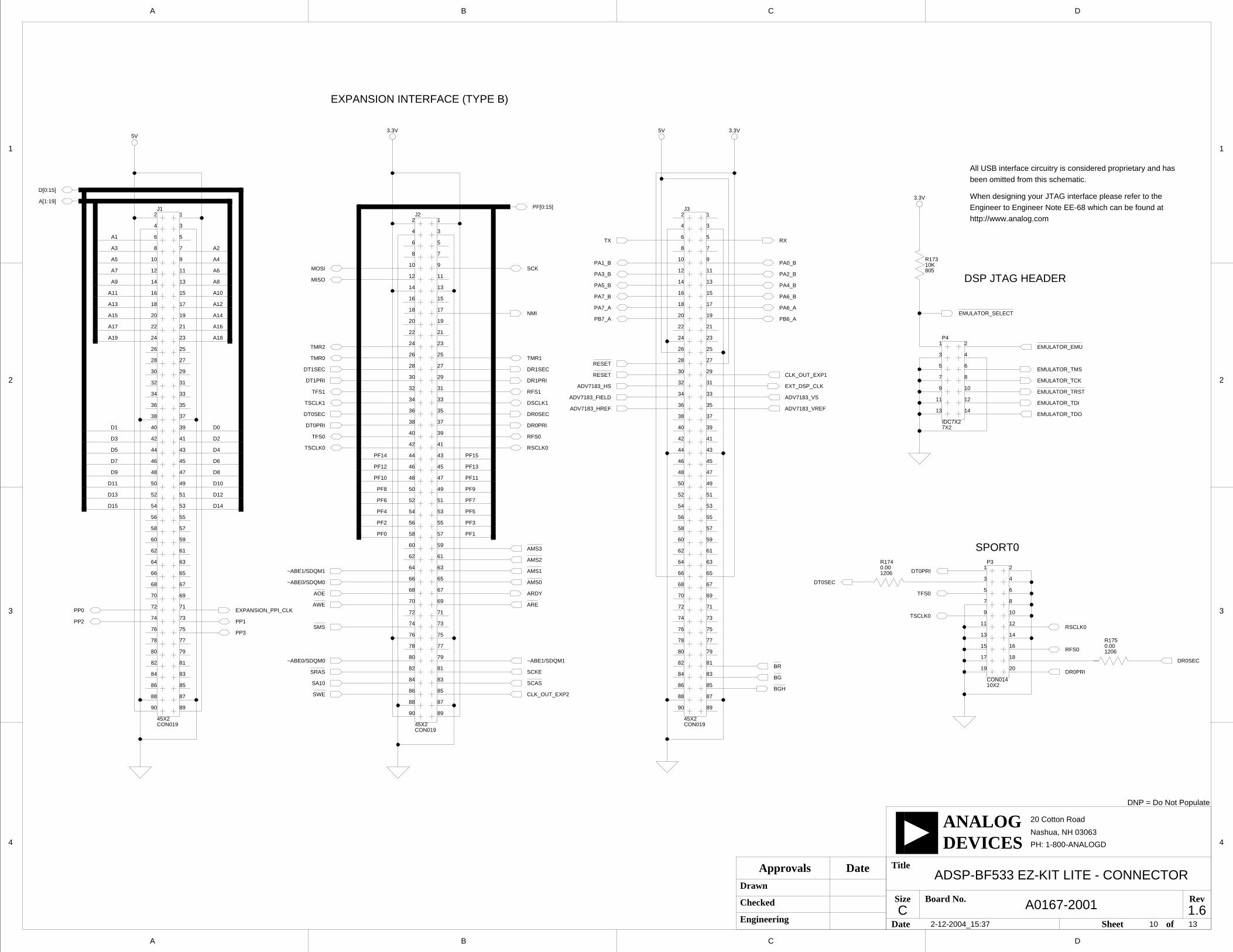
A0167-2001 1.6
4
3
2
1
A B C D
Nashua, NH 03063
A B C D
4
3
2
1
PH: 1-800-ANALOGD
C
Approvals Date
Drawn
Checked
Engineering Date
Size
Title
Board No. Rev
Sheet of
DEVICESANALOG 20 Cotton Road
DNP = Do Not Populate
5V
3.3V
5V 3.3V3.3V
SPORT0
EXPANSION INTERFACE (TYPE B)
All USB interface circuitry is considered proprietary and hasbeen omitted from this schematic.
When designing your JTAG interface please refer to theEngineer to Engineer Note EE-68 which can be found athttp://www.analog.com
DSP JTAG HEADER
13102-12-2004_15:37
1
3
5
7
9
11
13
2
4
6
8
10
12
14
P4
IDC7X27X2
CLK_OUT_EXP2
CLK_OUT_EXP1
A1
A2
A18
A16
A14
A12
A10
A8
A6
A4
A19
A17
A15
A13
A11
A9
A7
A5
A3
A[1:19]
87
85
83
81
77
75
73
69
67
65
63
61
59
57
1
10
1112
1314
1516
1718
19
2
20
2122
2324
2526
2728
29
3
30
3132
3334
3536
3738
39
4
40
4142
4344
4546
4748
5
50
6
78
9
49
55
51
53
52
54
56
58
60
62
66
70
68
72
74
76
78
80
82
84
86
88
90 89
64
71
79
J1
45X2CON019
PP1
PP3
PF10
PF12
PF14
PF2
PF6
PF8
PF13
PF11
PF9
PF7
PF5
PF3
PF15
PF1PF0
PF4
PF[0:15]
BGH
BG
BR
DT0SEC
RSCLK0
DR0PRI
DR0SEC
0.001206
R175
EMULATOR_TCK
EMULATOR_TMS
EXT_DSP_CLK
EMULATOR_TDO
EMULATOR_TDI
EMULATOR_TRST
PB6_A
PA6_APA7_A
PB7_A
ADV7183_VREF
ADV7183_FIELD ADV7183_VS
ADV7183_HS
NMI
EMULATOR_EMU
5
2
4
8
10
6
1
3
9
11
13
15
17
19
12
14
16
20
18
7
10X2CON014
P3
87
85
83
81
77
75
73
69
67
65
63
61
59
57
1
10
1112
1314
1516
1718
19
2
20
2122
2324
2526
2728
29
3
30
3132
3334
3536
3738
39
4
40
4142
4344
4546
4748
5
50
6
78
9
49
55
51
53
52
54
56
58
60
62
66
70
68
72
74
76
78
80
82
84
86
88
90 89
64
71
79
CON01945X2
J3
10K805
R173
TX RX
TSCLK0
TSCLK0
TSCLK1 DSCLK1
RSCLK0
SCK
EXPANSION_PPI_CLK
PP2
PP0
~ABE1/SDQM1
SRAS
SWE
D[0:15]
D10
D14
D12
D4
D6
D8
D0
D2D3
D5
D7
D9
D11
D13
D15
D1
RESET
ADSP-BF533 EZ-KIT LITE - CONNECTOR
RFS0
DT0PRI
TFS0
EMULATOR_SELECT
12060.00R174
RESET
MISO
DT1SEC
DT1PRI
TFS1 RFS1
DR1PRI
DR1SEC
ARE
SMS
SCKE
TMR2
TMR0
AMS0
AMS1
AMS2
AMS3
ARDY
~ABE1/SDQM1
AWE
SA10 SCAS
~ABE0/SDQM0
~ABE0/SDQM0
AOE
DR0SEC
DR0PRI
RFS0TFS0
DT0PRI
DT0SEC
TMR1
MOSI
87
85
83
81
77
75
73
69
67
65
63
61
59
57
1
10
1112
1314
1516
1718
19
2
20
2122
2324
2526
2728
29
3
30
3132
3334
3536
3738
39
4
40
4142
4344
4546
4748
5
50
6
78
9
49
55
51
53
52
54
56
58
60
62
66
70
68
72
74
76
78
80
82
84
86
88
90 89
64
71
79
J2
45X2CON019
ADV7183_HREF
PA6_B
PA4_B
PA2_B
PA0_B
PA5_B
PA7_B
PA3_B
PA1_B

SHGND
SHGND
1.8V
5V A5V
A1.8V3.3V
SHGND
GNDINPUT OUTPUT
3.3V
A0167-2001 1.6
4
3
2
1
A B C D
Nashua, NH 03063
A B C D
4
3
2
1
PH: 1-800-ANALOGD
C
Approvals Date
Drawn
Checked
Engineering Date
Size
Title
Board No. Rev
Sheet of
DEVICESANALOG 20 Cotton Road
DNP = Do Not Populate
SHGND
3.3VGND
INPUT OUTPUT
GNDINPUT OUTPUT
GNDINPUT OUTPUT
CHOKE_COIL
OUT1
OUT2
OUT3
IN1
IN2
FBSD GND
OUT1
OUT2
OUT3
IN1
IN2
FBSD GND
A3V
JUMPERSHORTING
SW10: Core Voltage Source Select
Position
1 and 2
Function
be populated and the DSP_VDD_INT will be hard-wired with R222to use the processor internal regulator.
DSP_VDD_INT = 1.4V Fixed
DSP_VDD_INT = DSP Internal Voltage Regulation
Note: For boards without a 750MHz processor this jumper will not
2 and 3
DEFAULT: 2 & 3
3
1
2
JP3
IDC3X13X1
SJ1
DEFAULT=2 & 3
13112-19-2004_13:19
DNP
0.00805
R211
1V4
DSP_VDD_INT
64.9KR184
805
340KR185
805
8051UFC61
CT28
D68UF
IND00110UHL12
0.00805
R222
TP12
TP15
4
3
2
1
8
7
6
5
U32
SO-8NDS8434A
3.32KR223
805
VROUT
UNREG_IN
8051UFC103
10K805
R192
10K805
R214
8051UFC102
1206FER20
147KR191
1206
76.8KR190
1206
1
2
3
7
8
56
4MSOP8ADP3336ARM
VR2
1
2
3
7
8
56
4MSOP8ADP3336ARM
VR6
DSP_VDD_INT
VDDRTC
8050.00R186
8050.00R187
DSP_VDD_EXT
CT13
C10UF
CT24
C10UF
2ADO-214AA
D4
UNREG_IN
4
1
3
2
FER23
FUS0012.5AF1
8050.00R210
8051UFC60
8051UFC104
C105
8050.1UF
0.00805
R188
8050.00R189
12060.00R177
TP11
3
1
2
ADP3339AKC-5SOT-223
VR5
2
1
3
VR3
SOT-223ADP3339AKC-33
3
1 1A
ZHCS1000SOT23D
D5
DSP_VDD_EXT
3
1
2
ADP3339AKC-33SOT-223
VR4
8050.1UFC98
10UFC
CT230.1UF805
C175
C10UFCT21
C1000.1UF805
0.001206
R178
10UFC
CT26
UNREG_IN
TP10
12061000PFC96
DO-214AA2AD3
12061000PFC97
1
3
2
CON0052.5MM_JACK
7.5V_POWER
J9
ADSP-BF533 EZ-KIT LITE - POWER
1206600FER18
3V_B
2
1
3
ADP3338AKC-33SOT-223
VR1
TP8
1206600FER19
UNREG_IN
6001206
FER21
MH2 MH1 MH5MH4MH3
DO-214AA2AD2
1206100KR176
C10UFCT22
1206600FER22
TP9
8050.1UFC143
TP14 TP13
CT2510UFC
8050.1UFC101
C10UFCT27
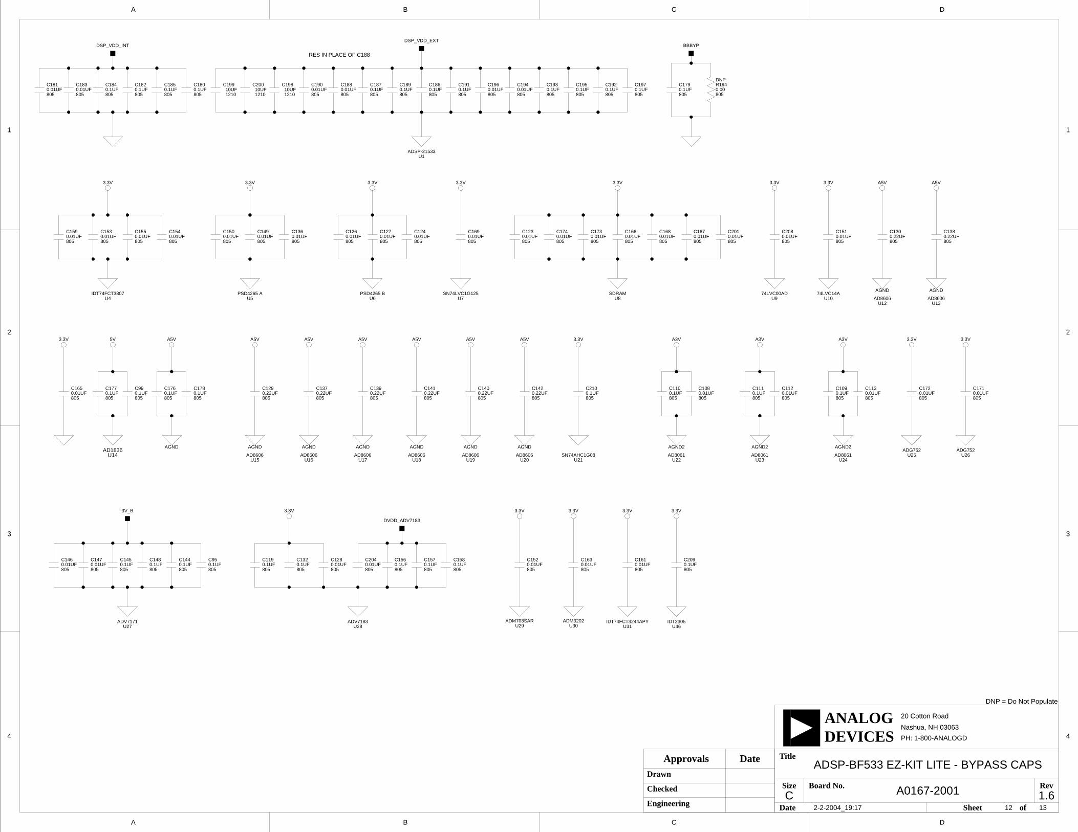
3.3V
AGND2
3.3V3.3V
3.3V3.3V3.3V3.3V3.3V3.3V
3.3V 3.3V
A0167-2001 1.6
4
3
2
1
A B C D
Nashua, NH 03063
A B C D
4
3
2
1
PH: 1-800-ANALOGD
C
Approvals Date
Drawn
Checked
Engineering Date
Size
Title
Board No. Rev
Sheet of
DEVICESANALOG 20 Cotton Road
DNP = Do Not Populate
A3V A3V A3VA5V A5VA5V
AGND
AGND AGND AGND
A5V
AGND
A5V
AGND
AGND
A5V
AGND
A5V A5V
5V
AGND
A5V
3.3V
3.3V3.3V
3.3V
AGND2AGND2
3.3V
RES IN PLACE OF C188
AD8606 AD8606AD8606AD8606 AD8606 AD8061AD8061U23 U24U22
AD8061U15 U17U16 U20U18
U4IDT74FCT3807
ADG752 ADG752U26U25
U30ADM3202
U29ADM708SARADV7171
U27ADV7183
U28IDT74FCT3244APY
U31
AD1836U14
PSD4265 AU5
PSD4265 BU6
SN74LVC1G125U7
SDRAMU8
74LVC00ADU9
74LVC14AU10 AD8606
U12AD8606
U13
ADSP-21533
AD8606U19
IDT2305U46
U21SN74AHC1G08
U1
2-2-2004_19:17 12 13
8050.01UFC188
8050.01UFC190
DSP_VDD_EXT
8050.01UFC146
0.01UF805
C1470.1UF805
C145
8050.1UFC148
0.1UF805
C1440.1UF805
C95
8050.1UFC119
8050.1UFC132
0.01UF805
C128 C204
8050.01UF
8050.1UFC156
0.1UF805
C157
8050.1UFC158
0.01UF805
C1520.01UF805
C1630.01UF805
C161
8050.01UFC171
8050.01UFC172
8050.01UFC113
8050.1UFC109C112
8050.01UF0.1UF
805
C1110.01UF805
C108
8050.1UFC110
0.22UF805
C1420.22UF805
C1400.22UF805
C1410.22UF805
C1390.22UF805
C1370.22UF805
C1290.1UF805
C178
8050.1UFC176
8050.1UFC99
8050.1UFC177
0.01UF805
C165
0.22UF805
C138
8050.22UFC130
0.01UF805
C151C208
8050.01UF
C201
8050.01UF
8050.01UFC167
8050.01UFC168
8050.01UFC166
8050.01UFC173
0.01UF805
C1740.01UF805
C1230.01UF805
C1690.01UF805
C124
8050.01UFC127
8050.01UFC126
0.01UF805
C136
8050.01UFC149
8050.01UFC150C154
8050.01UF0.01UF
805
C155
8050.01UFC153
0.01UF805
C159
0.1UF805
C197
8050.1UFC192
0.1UF805
C195
8050.1UFC193
8050.01UFC194
0.01UF805
C196
8050.1UFC191
0.1UF805
C186
8050.1UFC189
0.1UF805
C18710UF1210
C19810UF1210
C200
121010UF
C1990.01UF805
C181
8050.01UFC183
8050.1UFC184
0.1UF805
C182
8050.1UFC185
0.1UF805
C180
8050.00
DNPR194
8050.1UFC179
ADSP-BF533 EZ-KIT LITE - BYPASS CAPS
BBBYPDSP_VDD_INT
DVDD_ADV7183
3V_B
8050.1UFC209
C2100.1UF805
I INDEX
Symbols peripheral ports, -xiv
~AMS0, memory select pin, 2-3, 2-6,3-3~AMS1, memory select pin, 2-3, 2-6,
3-3~AMS2, memory select pin, 2-3, 2-6,
3-3~SMS0, memory select pin, 2-2, 3-3
AAD1836, 2-11, 3-4, 3-12Add New Hardware Wizard, Windows
98, 1-8ADSP-BF533 processor
address space, 2-6audio interface, see SPORT0Clock In (CLK IN), 3-7Clock Out (CLK OUT), 3-3core voltage, 3-2External Bus Interface Unit (EBIU),
3-3input clock, 3-3internal memory restrictions, 2-2internal SRAM, 2-2IO voltage, 3-2memory map, 2-2parallel peripheral interface (PPI), 3-5
real time clock (RTC), 3-3ADV7171, video encoder, 2-12, 3-6,
3-7, 3-11ADV7183, video decoder, 2-12, 3-6,
3-7, 3-11ASYNC, memory banks 0-3, 2-3audio
applications, -xivcodec, 2-11connectors (J4, J5), 3-17interface, see SPORT0see also AD1836
Bbackground telemetry channel (BTC),
2-13bill of materials, A-1boot
load, 2-16mode select (JP1-2), 3-10
breakpoints, restrictions, 2-19
Cclock frequency, 2-4, 2-5codecs, 3-4configuration registers (IO), 2-6
ADSP-BF533 EZ-KIT Lite Evaluation System Manual I-1

INDEX
connecting, EZ-KIT Lite board, 1-5connectors, 1-5, 3-16
extender connectors (P3-1), 3-3FlashLINK (P1), 3-18J1 (expansion interface), 3-8J10 (USB), 1-6J2 (expansion interface), 3-8J3 (expansion interface), 3-8J4 (audio), 3-17J5 (audio), 3-17J8 (video), 3-17J9 (power), 3-17P4 (JTAG), 3-9, 3-20P9 (SPORT0), 3-19RS232 (P2), 3-19see also expansion interface
contents, EZ-KIT Lite package, 1-1conventions, manual, -xxiicore
frequency, 2-5voltage, 3-10
customer support, -xvi
DDevice Manager window, 1-16DIP switches, 3-9
see SWdual bank Flash memory, 2-3
EEBIU_SDBCTL, 2-4EBIU_SDGCTL, 2-4EBIU_SDRRC, 2-4electrostatic discharge, 1-2
emulation events, 2-16example programs, 2-13exceptions, 2-16expansion
board, 2-8interface, 3-4, 3-8, 3-16
extender connectors (P3-1), 3-3external
bus interface unit (EBIU), 3-3flash memory, see flash memoryregulator, 3-2, 3-10
external memory, 3-9bank 0 (primary A), 2-3bank 0 (SDRAM), 2-3
EZ-KIT Lite boardarchitecture, 3-2features, -xii
Ffeatures, EZ-KIT Lite board, -xiiflag pins, see programmable flags (PFs)flash A, 2-7
configuration registers, 2-8port A controls, 2-8port B controls, 2-9primary, 2-7registers, 2-7secondary, 2-7SRAM, 2-7
flash B, 2-7configuration registers, 2-8primary, 2-7registers, 2-7secondary, 2-7
I-2 ADSP-BF533 EZ-KIT Lite Evaluation System Manual
INDEX
SRAM, 2-7flash memory, -xiii, 2-5, 3-3, 3-10
configuring, 2-9general-purpose IO pins (U5), 3-15map, 2-6modifying, PSDsoft Express, 2-9primary, 2-3, 3-3programming, FlashLINK, 2-9reserved, 2-7secondary, 3-3
flash ports, PB0-5, 3-15Found New Hardware Wizard
Windows 2000, 1-14frequency, 2-4, 2-5
Ggeneral-purpose IO, 2-10, 2-11graphical user interface (GUI), 2-13
Hhard reset, 2-16Help, online, -xxHSYNC signal, 3-6, 3-7, 3-11
II2S mode, 2-11installation, summary, 1-3installing
EZ-KIT Lite USB driver, 1-7VisualDSP++ and EZ-KIT Lite
license, 1-5VisualDSP++ and EZ-KIT Lite
software, 1-4interfaces
SDRAM, 2-4see graphical user interface (GUI)
internalregulator, 3-2
internal memory, 2-3, 3-9core MMRs, 2-3data bank A SRAM, 2-3data bank B SRAM, 2-3instruction SRAM, 2-3instruction SRAM/CACHE, 2-3reserved, 2-3scratch pad SRAM, 2-3system MMRs, 2-3
IOconfiguration registers, 2-6signals, 2-7voltage, 3-2
IO port registers, 2-7Data In, 2-7Data Out, 2-8Direction, 2-7
JJTAG
connector (P4), 3-20emulation port, 3-9programming cable, 2-10
jumpers, 1-5, 3-9JP1-2 (boot mode select), 3-10JP3 (core voltage source select), 3-10
LLEDs, 1-5, 2-10, 3-13
LED1, 1-6, 3-14
ADSP-BF533 EZ-KIT Lite Evaluation System Manual I-3
INDEX
LED11, 1-15, 1-16, 3-15LED2-3, 1-6, 3-14LED4-9, 2-9, 3-15
license restrictions, 2-2
Mmemory, 2-4
flash configuration, 2-6SDRAM configuration, 2-4select pins, see ~AMS0, ~AMS1,
~AMS2, ~SMS0memory map, see ADSP-BF533
processor
PP3, SPORT connector, 3-4package contents, 1-1Parallel Peripheral Interface (PPI), -xiv,
2-12, 3-5PC
configuration, 1-3parallel port, 2-10
Performance Monitor Control dialog box, 2-15
PFs, see programmable flagspower
connector (J9), 3-17specifications, 3-18supply, 3-18
PPI interface, 2-12, 3-7primary flash memory, 2-6primary processor pins
PF3, 3-6PPI_CLK, 3-6
PPI0-7, 3-6TMR1-2, 3-6
processor memory map, see ADSP-BF533 processor
programmable flags (PFs), 3-4, 3-5PF0, 2-12, 3-4PF1, 2-12PF10-11, 3-5, 3-12, 3-14PF12-15, 3-5, 3-6PF2, 2-12, 3-4, 3-11PF3, 3-4PF4, 2-11, 3-4PF5-7, 3-5PF8-11, 2-10, 3-5, 3-12, 3-14PF9, 3-5, 3-12, 3-14push buttons, see also push buttons
push buttons, 2-10, 3-13connecting to PF pins, 3-13SW4-7 (general input), 3-5, 3-12,
3-14SW8 (reset), 3-14SW9 (enable), 2-11, 3-12, 3-13
Rregistering, this product, 1-2, 1-5regulators, 3-2, 3-10reset
board, 2-16options, 2-17processor, 3-14push button (SW8), 3-14service routines, 2-14
RFS0, signal, 3-12RSCLK0
I-4 ADSP-BF533 EZ-KIT Lite Evaluation System Manual
INDEX
register, 2-11signals, 3-12
SSCLK, 2-4, 2-5SDRAM, -xiii, 2-2, 2-3, 2-4, 2-5, 3-3secondary flash memory, 2-6serial
clock (SCL), 2-4, 2-12data (SDAT), 2-12
Serial Peripheral Interconnect (SPI), 3-4setting
EZ-KIT Lite hardware, 1-5target options, 2-17
software breakpoints, 2-19SPI port, 2-11SPORT0, -xiv, 2-11, 3-4, 3-12, 3-19SRAM, 2-3, 2-6, 3-3starting VisualDSP++, 1-16SW1-2, test DIP switches, 3-11SW3, DIP switch, 2-12, 3-7, 3-9, 3-11system
architecture, EZ-KIT Lite board, 3-2clock, 2-4requirements, PC, 1-3
Ttarget options
dialog box, 2-17miscellaneous, 2-18on emulator exit, 2-17reset, 2-17
test DIP switches (SW1-2), 3-11TFS0 signal, 3-12
TMR1-2, primary processor pins, 3-6trace
buffer, 2-14destination, 2-15instruction addresses, 2-15number, 2-15source, 2-15
trace window, 2-14, 2-15TSCLK0
register, 2-11signal, 3-12
UUART port, 3-8Universal Asynchronous Receiver
Transmitter (UART), -xiii, -xivUSB
cable, 1-2connector (P7), 3-18, 3-19driver installation, Windows 2000,
1-12driver installation, Windows 98, 1-8driver installation, Windows XP, 1-13interface, 3-9interface chip (U34), 3-14monitor LED (LED11), 3-15
user LEDs (LED9-4), 3-15see also LEDs
Vverifying USB driver installation, 1-15video, 2-12
configuration switch (SW3), 3-11connector (J8), 3-17
ADSP-BF533 EZ-KIT Lite Evaluation System Manual I-5
INDEX
decoder, -xivencoder, -xivinput mode, 3-7interface, 2-12output mode, 3-7
VisualDSP++documentation, -xx
installation, 1-4license, 1-5online Help, -xxrequirements, 1-3starting, 1-16
voltage regulators, 3-2VSYNC signal, 3-6, 3-7, 3-11
I-6 ADSP-BF533 EZ-KIT Lite Evaluation System Manual