adsp-2100 family ez-kit lite reference manual,...
TRANSCRIPT

EZ-KIT LiteReference Manual
ADSP-2100 Family
a

ADSP-2100 Family EZ-KIT LiteADSP-2100 Family EZ-KIT LiteADSP-2100 Family EZ-KIT LiteADSP-2100 Family EZ-KIT LiteADSP-2100 Family EZ-KIT LiteReference ManualReference ManualReference ManualReference ManualReference Manual 1995 Analog Devices, Inc.ALL RIGHTS RESERVED
PRODUCT AND DOCUMENTATION NOTICE: Analog Devices reserves the right to change this productand its documentation without prior notice.
Information furnished by Analog Devices is believed to be accurate and reliable.However, no responsibility is assumed by Analog Devices for its use, nor for any infringement of patents,or other rights of third parties which may result from its use. No license is granted by implication orotherwise under the patent rights of Analog Devices.
EZ-ICE and EZ-LAB are trademarks of Analog Devices, Inc.MS-DOS and Windows are trademarks of Microsoft, Inc.
PRINTED IN U.S.A.
Printing HistoryFIRST EDITION 5/95

For marketing information or Applications Engineering assistance, contact your localAnalog Devices sales office or authorized distributor.
If you have suggestions for how the ADSP-2100 Family EZ-KIT Lite or documentationcan better serve your needs, or you need Applications Engineering assistance fromAnalog Devices, please contact:
Analog Devices, Inc.DSP Applications EngineeringOne Technology WayNorwood, MA 02062-9106Fax: (617) 461-3010e-mail: [email protected]
The DSP Applications Engineering group runs a Bulletin Board Service that providesanswers to many DSP questions and information on Analog Devices DSP products.The BBS can be reached at speeds up to 14,400 baud, no parity, 8 bits data, 1 stopbit, dialing (617) 461-4258. This BBS supports: V.32bis, error correction (V.42 andMNP classes 2, 3, and 4), and data compression (V.42bis and MNP class 5)
Please submit any technical questions or problems in writing and send it to the e-mailaddress listed, the fax number listed, or to the BBS.
The DSP Applications Group also maintains an Internet FTP site. Login as anonymoususing your email address for your password. Type (from your UNIX prompt):
ftp ftp.analog.com (or type: ftp 137.71.23.11)

EZ-KIT Lite Hardware WarrantyEZ-KIT Lite Hardware WarrantyEZ-KIT Lite Hardware WarrantyEZ-KIT Lite Hardware WarrantyEZ-KIT Lite Hardware WarrantyYour EZ-KIT Lite hardware is warranted against defects in workmanshipand materials under normal use and service for 90 days from the date ofshipment by Analog Devices. This warranty does not extend to any unitswhich have been subjected to misuse, neglect, accident, or improperinstallation or application, or which have been repaired or altered byothers. Analog Devices’ sole liability and the Purchaser’s sole remedyunder this warranty is limited to repairing or replacing defective products.The repair or replacement of defective products does not extend thewarranty period. Analog Devices, Inc. shall not be liable for consequentialdamages under any circumstances.
EZ-KIT Lite Hardware ServiceEZ-KIT Lite Hardware ServiceEZ-KIT Lite Hardware ServiceEZ-KIT Lite Hardware ServiceEZ-KIT Lite Hardware ServiceUse the following procedure if you have a hardware problem with yourEZ-KIT Lite:
• Describe the situation in written form and send it to the DSPApplications Group as described on the previous page. Make sure toinclude any source code examples or special circumstances that willhelp with problem diagnoses.
• You will receive a confirmation notice that explains a work-around toyour problem. If it is determined that the problem lies in your EZ-KITLite, you will be directed to a sales representative to set up an EZ-KITLite product return.
• The Sales Representative will provide you with a Material ReturnAuthorization number (MRA#) and the address to which you shouldsend your EZ-KIT Lite Product. (See the following notes.)
All Returns: The MRA# must be written on the box for AnalogDevices Receiving to accept shipment.
Warranty Returns: As mentioned in the warranty, the warranty periodbegins with the shipment date. This information ison the invoice for your EZ-KIT Lite Product. Youmust provide the Sales Representative with theshipment date information to obtain a warrantyrepair.
EZ-KIT Lite Returns: After the 90 day warranty, no repair is available forthe EZ-KIT Lite.

LiteratureLiteratureLiteratureLiteratureLiteratureThe following is a list of related literature. Literature can be obtained/purchased from your local Analog Devices sales office or authorizeddistributor.
ADSP-2100 Family User’s Manual (Prentice Hall)Complete description of processor architectures and system interfaces.
ADSP-2171/81 User’s ManualInformation specific to the ADSP-2181.
ADSP-2100 Family Assembler Tools & Simulator ManualADSP-2100 Family C Tools ManualADSP-2100 Family C Runtime Library ManualProgrammer’s references.
APPLICATIONS INFORMATIONAPPLICATIONS INFORMATIONAPPLICATIONS INFORMATIONAPPLICATIONS INFORMATIONAPPLICATIONS INFORMATION
Digital Signal Processing Applications Using the ADSP-2100 Family,Volume 1 (Prentice Hall)Topics include arithmetic, filters, FFTs, linear predictive coding, modemalgorithms, graphics, pulse-code modulation, multirate filters, DTMF,multiprocessing, host interface and sonar.
Digital Signal Processing Applications Using the ADSP-2100 Family,Volume 2 (Prentice Hall)Topics include modems, linear predictive coding, GSM codec, sub-bandADPCM, speech recognition, discrete cosine transform, digital tonedetection, digital control system design, IIR biquad filters, software uartand hardware interfacing.
SPECIFICATION INFORMATIONSPECIFICATION INFORMATIONSPECIFICATION INFORMATIONSPECIFICATION INFORMATIONSPECIFICATION INFORMATION
ADSP-21xx Data SheetADSP-2181 Data SheetAD1847 Data Sheet

22222
2 – 12 – 12 – 12 – 12 – 1
ContentsContentsContentsContentsContents
CHAPTER 1CHAPTER 1CHAPTER 1CHAPTER 1CHAPTER 1 INTRODUCTIONINTRODUCTIONINTRODUCTIONINTRODUCTIONINTRODUCTION
INTRODUCTION ................................................................................................. 1–1UNPACKING ....................................................................................................... 1–1EZ-KIT LITE......................................................................................................... 1–1CONTENTS OF THIS MANUAL ......................................................................... 1–2
CHAPTER 2CHAPTER 2CHAPTER 2CHAPTER 2CHAPTER 2 UPGRADE INFORMATIONUPGRADE INFORMATIONUPGRADE INFORMATIONUPGRADE INFORMATIONUPGRADE INFORMATION
OVERVIEW ......................................................................................................... 2–1UPGRADE DESCRIPTION ................................................................................. 2–1
CHAPTER 3CHAPTER 3CHAPTER 3CHAPTER 3CHAPTER 3 GETTING STARTEDGETTING STARTEDGETTING STARTEDGETTING STARTEDGETTING STARTED
OVERVIEW ......................................................................................................... 3–1QUICK START SOFTWARE INSTALLATION .................................................... 3–2REQUIREMENTS................................................................................................ 3–3QUICK START HARDWARE INSTALLATION ................................................... 3–4
CHAPTER 4CHAPTER 4CHAPTER 4CHAPTER 4CHAPTER 4 INSTALLATION PROCEDURESINSTALLATION PROCEDURESINSTALLATION PROCEDURESINSTALLATION PROCEDURESINSTALLATION PROCEDURES
SOFTWARE INSTALLATION ............................................................................. 4–1SOFTWARE INSTALLATION PROCEDURE ..................................................... 4–1
Make Working Copies Of The Diskettes .................................................... 4–1Modify Your CONFIG.SYS File .................................................................. 4–1Install The Software On Your Hard Disk .................................................... 4–2
ENVIRONMENT VARIABLES ............................................................................. 4–3HARDWARE INSTALLATION ............................................................................. 4–3

33333 ContentsContentsContentsContentsContents
2 – 22 – 22 – 22 – 22 – 2
CHAPTER 5CHAPTER 5CHAPTER 5CHAPTER 5CHAPTER 5 DSP SYSTEM DEVELOPMENTDSP SYSTEM DEVELOPMENTDSP SYSTEM DEVELOPMENTDSP SYSTEM DEVELOPMENTDSP SYSTEM DEVELOPMENT
OVERVIEW ......................................................................................................... 5–1System Requirements ................................................................................ 5–1System Design ........................................................................................... 5–2Architecture Description File ...................................................................... 5–2Code Development ..................................................................................... 5–3Running The Assembler ........................................................................... 5–11Running The Linker .................................................................................. 5–11Running The Simulator ............................................................................. 5–12Programming An EPROM ........................................................................ 5–12Running The ADSP-2181 EZ-KIT Lite Board ........................................... 5–13Debugging ................................................................................................ 5–13
CHAPTER 6CHAPTER 6CHAPTER 6CHAPTER 6CHAPTER 6 EZ-KIT LITE HOST PROGRAMEZ-KIT LITE HOST PROGRAMEZ-KIT LITE HOST PROGRAMEZ-KIT LITE HOST PROGRAMEZ-KIT LITE HOST PROGRAM
PROGRAM OVERVIEW ..................................................................................... 6–1COMMAND SUMMARY ...................................................................................... 6–2DETAILED COMMANDS .................................................................................... 6–3
File Menu .................................................................................................... 6–3View Menu .................................................................................................. 6–4
Toolbar ............................................................................................... 6–4Status Bar .......................................................................................... 6–6
Demo Menu ................................................................................................ 6–6DTMF ................................................................................................. 6–6Filtering .............................................................................................. 6–8Echo Cancellation .............................................................................. 6–9ADPCM ............................................................................................ 6–107.8k LPC .......................................................................................... 6–112.4k LPC .......................................................................................... 6–12
Floating Menu ........................................................................................... 6–12Loading Menu ........................................................................................... 6–13
Download User Program and Go .................................................... 6–13Download User Program ................................................................. 6–15Go .................................................................................................... 6–15Upload Data Memory ....................................................................... 6–16Upload Program Memory ................................................................ 6–17Download Data Memory .................................................................. 6–18Download Program Memory ............................................................ 6–19
Options Menu ........................................................................................... 6–20Settings ............................................................................................ 6–21List Of Demos .................................................................................. 6–21

33333ContentsContentsContentsContentsContents
2 – 32 – 32 – 32 – 32 – 3
Help Menu ................................................................................................ 6–22About EZ-KIT ................................................................................... 6–22
User Configurable Settings ...................................................................... 6–22Error Messages & Troubleshooting ................................................. 6–23
RUNNING DEMOS ........................................................................................... 6–26CREATING YOUR OWN PROGRAMS ............................................................ 6–27
CHAPTER 7CHAPTER 7CHAPTER 7CHAPTER 7CHAPTER 7 EZ-KIT LITE MONITOR PROGRAMEZ-KIT LITE MONITOR PROGRAMEZ-KIT LITE MONITOR PROGRAMEZ-KIT LITE MONITOR PROGRAMEZ-KIT LITE MONITOR PROGRAM
PROGRAM OVERVIEW ..................................................................................... 7–1MONITOR FEATURES ....................................................................................... 7–1RESTRICTIONS .................................................................................................. 7–1CREATING YOUR OWN PROGRAMS TO BE USED WITH THE MONITOR.... 7–2DEBUGGING....................................................................................................... 7–5DSP MEMORIES................................................................................................. 7–6
CHAPTER 8CHAPTER 8CHAPTER 8CHAPTER 8CHAPTER 8 EZ-KIT LITE HARDWARE DESCRIPTIONEZ-KIT LITE HARDWARE DESCRIPTIONEZ-KIT LITE HARDWARE DESCRIPTIONEZ-KIT LITE HARDWARE DESCRIPTIONEZ-KIT LITE HARDWARE DESCRIPTION
DESIGN OVERVIEW .......................................................................................... 8–1SPECIFICATIONS .............................................................................................. 8–3CONNECTORS ................................................................................................... 8–3SWITCHES.......................................................................................................... 8–4INDICATORS ...................................................................................................... 8–5HARDWARE OPERATION ................................................................................. 8–5HARDWARE EXPANSION ................................................................................. 8–5EXPANSION CONNECTORS ............................................................................. 8–7HARDWARE DEBUGGING ................................................................................ 8–9
PROGRAMMER’S QUICK REFERENCEPROGRAMMER’S QUICK REFERENCEPROGRAMMER’S QUICK REFERENCEPROGRAMMER’S QUICK REFERENCEPROGRAMMER’S QUICK REFERENCE
SCHEMATICSSCHEMATICSSCHEMATICSSCHEMATICSSCHEMATICS

11111
1 – 11 – 11 – 11 – 11 – 1
IntroductionIntroductionIntroductionIntroductionIntroduction
INTRODUCTIONINTRODUCTIONINTRODUCTIONINTRODUCTIONINTRODUCTIONCongratulations! Your EZ-KIT Lite is one of the most cost effective,powerful development systems available on the market. The ADSP-2181used in the EZ-KIT Lite offers the highest integration and performance inthe 16-bit fixed-point DSP processor arena with 32K words of on-chipRAM, 30 ns instruction cycle time, DMA ports, and low power modes.
UNPACKINGUNPACKINGUNPACKINGUNPACKINGUNPACKINGYour EZ-KIT Lite should contain the following items.
• ADSP-2181 Development Board• 3.5" Software Diskette• EZ-KIT Lite Manual• DB9 to DB9 RS-232 Cable• Power Supply (US only)
If you are missing any items, please contact your Analog Devices salesoffice, authorized distributor, or reseller.
EZ-KIT LITEEZ-KIT LITEEZ-KIT LITEEZ-KIT LITEEZ-KIT LITEEZ-KIT Lite provides an easy way for you to investigate the power of theADSP-2100 Family of processors and develop your own applicationsbased on these high-performance DSPs. It is a complete developmentsystem package with a price that makes it ideal for getting started in DSPand the performance to take you through all the phases of thedevelopment process. With EZ-KIT Lite you can:
• Evaluate Analog Devices’ DSPs• Learn About DSP Applications• Develop DSP Applications• Simulate & Debug Your Application• Prototype Applications

11111 IntroductionIntroductionIntroductionIntroductionIntroduction
1 – 21 – 21 – 21 – 21 – 2
The EZ-KIT Lite consists of a small ADSP-2181 based development/demonstration board with full 16-bit stereo audio I/O capabilities. In thisdocumentation, this board may be referred to as either the ADSP-2181EZ-LAB® or the EZ-KIT Lite board. The terms are used interchangeably.The board’s features include:
• ADSP-2181 33 MIPS DSP• AD1847 Stereo SoundPort• RS-232 Interface• Socketed EPROM• User Pushbuttons• Power Supply Regulation• Expansion Connectors• User Configurable Jumpers
The board can run standalone or can simply connect to the RS-232 port ofyour PC. A monitor program running on the DSP in conjunction with ahost program running on the PC lets you interactively downloadprograms as well as interrogate the ADSP-2181. The board comes with asocketed EPROM so that you can run the monitor program anddemonstrations provided or you can plug in an EPROM containing yourown code.
The EZ-KIT Lite also comes with all the software you need to developsophisticated, high-performance DSP applications. An Assembler, Linker,PROM Splitter utility, and Simulator are all included.
CONTENTS OF THIS MANUALCONTENTS OF THIS MANUALCONTENTS OF THIS MANUALCONTENTS OF THIS MANUALCONTENTS OF THIS MANUALThis manual provides all the information you need to:
• Install the EZ-KIT Lite software on to an IBM compatible PersonalComputer
• Connect your EZ-KIT Lite to your PC• Connect your EZ-KIT Lite to the power supply• Connect an input source (such as a microphone or CD player) to your
EZ-KIT Lite• Connect an output device (such as an amplified/powered speaker)• Start the EZ-KIT Lite board• Use the software provided• Write your own ADSP-2181 programs to run on the EZ-KIT Lite board

11111IntroductionIntroductionIntroductionIntroductionIntroduction
1 – 31 – 31 – 31 – 31 – 3
Chapter 2 describes the general capabilities of the EZ-KIT Litedevelopment software and tells you what other features are available byupgrading to the ADSP-2100 Family Development Software.
Chapter 3 contains basic information on how to get started. It isrecommended that you read this manual completely and thoroughly,especially if you are new to programming a DSP processor. For those ofyou who can’t wait and are anxious to power up the EZ-KIT Lite andbegin tinkering, this chapter provides you with the basics to get up andrunning quickly.
Chapter 4 provides a detailed description for installing the varioussoftware modules on to an IBM compatible PC. These software modulesinclude:
• ADSP-2181 Development Software• EZ-KIT Lite Host Software• Demonstration Programs• Example Programs
This chapter also describes how to set up and use the EZ-KIT Lite board.
Chapter 5 provides an overview of the development process. This chaptershould give you most of the information you need to write your ownADSP-2181 programs. Complete source code for an example program islisted and described. You should be able to use this program as a basis forwriting your own program. Examples are also given for running theAssembler, Linker, and PROM Splitter.
Chapter 6 describes the operation of the host program. The host programruns under Windows™ on an IBM-compatible PC. The host program isused to communicate to the ADSP-2181 EZ-LAB.
Chapter 7 describes the DSP monitor program that is shipped with theEZ-KIT Lite. The EPROM installed on the EZ-KIT Lite board contains themonitor. This chapter also details the guidelines that you should follow tocreate your own DSP programs for use with the monitor.
Chapter 8 contains a detailed description of the EZ-KIT Lite hardware.Information concerning expanding the EZ-KIT Lite to better suit yourneeds is also provided.

11111 IntroductionIntroductionIntroductionIntroductionIntroduction
1 – 41 – 41 – 41 – 41 – 4
Programmer’s Quick Reference provides a quick reference of all theassembly language instructions for the ADSP-2181. It also describesoperation of the Assembler, Linker, PROM Splitter, and Simulator.
Schematics contains the schematic diagrams for the EZ-KIT Lite board.

22222
2 – 12 – 12 – 12 – 12 – 1
Upgrade InformationUpgrade InformationUpgrade InformationUpgrade InformationUpgrade Information
OVERVIEWOVERVIEWOVERVIEWOVERVIEWOVERVIEWEZ-KIT Lite is shipped with a version of software that is fullyfunctional for basic DSP development operations such as assembling,linking, simulating/debugging, and PROM formatting. With thissoftware, you can create a high performance ADSP-2181 based systemwith very sophisticated features. The EZ-KIT Lite software is morepowerful and complete than the software you find in some of the othermanufacturer’s DSP starter kits.
The Lite version is powerful enough to fill the needs of most users, butthose who want technical support and the full flexibility provided by aC compiler, C source-level debugger, a complete set of libraries, alibrarian, and all of the simulators for the entire ADSP-2100 Familymay want to upgrade to the standard development software for theADSP-2100 Family.
UPGRADE DESCRIPTIONUPGRADE DESCRIPTIONUPGRADE DESCRIPTIONUPGRADE DESCRIPTIONUPGRADE DESCRIPTIONIn addition to features found in the Lite version, the ADSP-2100 FamilyDevelopment Software adds:
• System BuilderDefine your target system hardware in an architecture descriptionfile. The Linker and the Simulator use this information to knowhow much memory is in your system, which memory is RAM andwhich is ROM, which memory is internal to the processor andwhich is external, and what memory-mapped peripherals youhave.
• SimulatorsRun an instruction level simulation of any ADSP-2100 Familyprocessor. All of the ADSP-2100 Family Simulators provide aninteractive, instruction-level simulation, displaying the cycle-by-cycle operation of different portions of the processor and systemhardware through a window-based graphical user interface.

22222 Upgrade InformationUpgrade InformationUpgrade InformationUpgrade InformationUpgrade Information
2 – 22 – 22 – 22 – 22 – 2
• LibrarianCombine frequently used subroutines into a single library file tosimplify the task of linking and streamline system software.
• C CompilerCode your applications in ANSI standard C. This compiler is basedon the industry-standard GNU C Compiler of the Free SoftwareFoundation.
• C Runtime LibraryUse this C callable library for ANSI standard and custom DSPfunctions. The C library includes functions for simplified interrupthandling with automatic save and restore of registers.
• C DebuggerSimplify the process of debugging your programs with this CSource Level Debugger which is integrated within the simulatorand emulator environments.
Compare and decide. A quick comparison of some of the featuresavailable in the EZ-KIT Lite software and the ADSP-2100 Familyappears on the facing page.

22222Upgrade InformationUpgrade InformationUpgrade InformationUpgrade InformationUpgrade Information
2 – 32 – 32 – 32 – 32 – 3
Features
EZ-KIT Lite
Software
ADSP-2100Family
Software
System Builder (Create your own architecture description files) √*
Assembler
Linker
ADSP-2101 Simulator (Also simulates ADSP-2103, ADSP-2105 and ADSP-2115)
ADSP-2111 Simulator
ADSP-2171 Simulator
ADSP-2181 Simulator
C Compiler
C Runtime Libraries
C Debugger
Full Set of Documentation
Technical Support
√
√
√
√
√
√
√
√
√
√
√
√
√
√
* EZ-KIT Lite is shipped with an architecture description file for the ADSP-2181
Prom Splitter √√
Development Software Comparison
Librarian √
33333
3 – 13 – 13 – 13 – 13 – 1
Getting StartedGetting StartedGetting StartedGetting StartedGetting Started
OVERVIEWOVERVIEWOVERVIEWOVERVIEWOVERVIEWThe EZ-KIT Lite contains the ADSP-2181 EZ-LAB evaluation board,ADSP-2181 Development Software, IBM PC compatible host software,example programs and demos, and documentation. You can obtainadditional information and documentation from your local AnalogDevices sales office or authorized distributor. You may find thisdocumentation useful if you are planning to do a significant amount ofADSP-2181 code development. The following documents can beobtained or purchased:
ADSP-2100 Family User’s ManualADSP-2100 Family Assembler Tools & Simulator ManualADSP-2181 User’s Manual
To fully utilize all the functions of the EZ-KIT Lite you will need toinstall the provided software on to an IBM compatible PC and connectthe EZ-KIT Lite board to the PC as well as connect it to a powersupply, analog input source and amplified speakers.

33333 Getting StartedGetting StartedGetting StartedGetting StartedGetting Started
3 – 23 – 23 – 23 – 23 – 2
QUICK START SOFTWARE INSTALLATIONQUICK START SOFTWARE INSTALLATIONQUICK START SOFTWARE INSTALLATIONQUICK START SOFTWARE INSTALLATIONQUICK START SOFTWARE INSTALLATIONThis section contains a very brief description of the EZ-KIT Litesoftware installation procedure. It is written for experienced PC usersfamiliar with installing software onto their PC.
The install utility for the EZ-KIT Lite should be run under Windows™.
1. Make sure Windows is running.
2. Insert EZ-KIT Lite Software disk into a floppy drive.(usually A: or B:)
3. Open the Program Manager window, if it is not already open.
4. From the File menu, select Run. The Run dialog box should appear.
5. In the “Command line” box type A:\SETUP.EXE( or B:\SETUP.EXE ).
6. Click on OK or press enter.
7. Follow the instructions on the screen.
Note: You will need to edit your AUTOEXEC.BAT file in the followingmanner.
1. Add the environment variable SET ADI_DSP=C:\ADI_DSP
2. Append to the path variable C:\ADI_DSP\21XX\BIN
A detailed installation procedure is described in the next chapter.

33333Getting StartedGetting StartedGetting StartedGetting StartedGetting Started
3 – 33 – 33 – 33 – 33 – 3
REQUIREMENTSREQUIREMENTSREQUIREMENTSREQUIREMENTSREQUIREMENTSTo run the EZ-KIT Lite software, you will need:
• 386- (or higher) based PC with a hard disk, high-density floppy diskdrive, color video card and VGA monitor, and a minimum of 2 MBextended RAM.
• 4 MB of free disk space to install the software.
• DOS 3.1 or higher.
• Microsoft Windows 3.1 or higher.
The setup program will create the following tree in the specifieddestination path:
21XX\BIN Assembler, linker, simulator, andsplitter DOS executables
21XX\ETC Error messages and simulator on-linehelp
21XX\INCLUDE 2181 header file 21XX\LIB 2181 architecture file 21XX\EZKITL Windows host program and demo
.EXE files 21XX\EZKITL\2181\MONITOR Source code and batch file for creating
monitor program 21XX\EZKITL\2181\DSP Source code and batch files for
creating demo .EXE files 21XX\EZKITL\2181\DSP\ADPCM 21XX\EZKITL\2181\DSP\DTMF 21XX\EZKITL\2181\DSP\ECHO 21XX\EZKITL\2181\DSP\FIRDEMO 21XX\EZKITL\2181\DSP\LPC2K4 21XX\EZKITL\2181\DSP\LPC7K8

33333 Getting StartedGetting StartedGetting StartedGetting StartedGetting Started
3 – 43 – 43 – 43 – 43 – 4
QUICK START HARDWARE INSTALLATIONQUICK START HARDWARE INSTALLATIONQUICK START HARDWARE INSTALLATIONQUICK START HARDWARE INSTALLATIONQUICK START HARDWARE INSTALLATIONThe diagram below shows where connections for power, RS-232, audioinput, and audio output are made. After all connections are made,apply power and press the reset button.
GreenPower
LED
RedFlag Out
LED
StereoAudio Input
StereoAudio Output
DCPower Supply
ConnectorSerial Port (RS232)
Connector
AD1847Stereo Codec
ADSP-2181Digital Signal
Processor
Socketed EPROM
J1
J2
LINE
MIC Input Source Selector
(Default Shown)
a
ADSP-2181EZ-KIT LITE
JP2
JP1
U3
U7
U2
P3
P2
P1
EZ-ICE
In-CircuitEmulator
Connector
EPROM Configuration
Jumper
Expansion Connectors
RESET INTERRUPT FL1
RESETButton
Processor InterruptButton
Pin 1
Pin 1
Pin 1
ADSP-2181 EZ-LAB Board DiagramADSP-2181 EZ-LAB Board DiagramADSP-2181 EZ-LAB Board DiagramADSP-2181 EZ-LAB Board DiagramADSP-2181 EZ-LAB Board Diagram
A detailed installation procedure is described in the next chapter.

44444
4 – 14 – 14 – 14 – 14 – 1
Installation ProceduresInstallation ProceduresInstallation ProceduresInstallation ProceduresInstallation Procedures
SOFTWARE INSTALLATIONSOFTWARE INSTALLATIONSOFTWARE INSTALLATIONSOFTWARE INSTALLATIONSOFTWARE INSTALLATIONA diskette is included in your EZ-KIT Lite package. You should runthe installation program contained on the diskette under Windows™.The installation program will create all the required directories andsubdirectories and install the appropriate files.
SOFTWARE INSTALLATION PROCEDURESOFTWARE INSTALLATION PROCEDURESOFTWARE INSTALLATION PROCEDURESOFTWARE INSTALLATION PROCEDURESOFTWARE INSTALLATION PROCEDUREThe software requires:
• 386- (or higher based) PC with a hard disk, high-density floppy diskdrive, color video card and VGA monitor, and a minimum of 2 MBextended RAM.
• 4 MB of free disk space to install the software.
• DOS 3.1 or higher.
• Microsoft Windows 3.1 or higher.
STEP 1:STEP 1:STEP 1:STEP 1:STEP 1: Make Working Copies Of The DiskettesMake Working Copies Of The DiskettesMake Working Copies Of The DiskettesMake Working Copies Of The DiskettesMake Working Copies Of The DiskettesBefore installing the software, you should copy the original disketteonto a working disk. This can be accomplished with either the XCOPYor COPY MS-DOS command (do not use the DISKCOPY command).The original disk should be stored in a safe place and used only tocreate a working disk.
STEP 2:STEP 2:STEP 2:STEP 2:STEP 2: Modify Your CONFIG.SYS FileModify Your CONFIG.SYS FileModify Your CONFIG.SYS FileModify Your CONFIG.SYS FileModify Your CONFIG.SYS FileTo ensure proper operation of the development software, add (ormodify) the directive FILES=25 in the CONFIG.SYS file (FILESmay also be set to a number greater than 25). You should also add (ormodify) the directive BUFFERS=30 in the CONFIG.SYS file. Aftermodifying the CONFIG.SYS file, the PC must be rebooted for thechange to take effect.

44444 Installation ProceduresInstallation ProceduresInstallation ProceduresInstallation ProceduresInstallation Procedures
4 – 24 – 24 – 24 – 24 – 2
STEP 3:STEP 3:STEP 3:STEP 3:STEP 3: Install The Software On Your Hard DiskInstall The Software On Your Hard DiskInstall The Software On Your Hard DiskInstall The Software On Your Hard DiskInstall The Software On Your Hard DiskFollow these directions to install the software on your hard disk.
1. Make sure Windows is running.
2. Insert EZ-KIT Lite Software disk into a floppy drive.(usually A: or B:)
3. Open the Program Manager window, if it is not already open.
4. From the File menu, select Run. The Run dialog box should appear.
5. In the “Command line” box type A:\SETUP.EXE( or B:\SETUP.EXE ).
6. Click on OK or press enter.
7. Follow the instructions on the screen.
Note: You will need to edit your AUTOEXEC.BAT file in the followingmanner.
1. Add the environment variable SET ADI_DSP=C:\ADI_DSP
2. Append to the path variable C:\ADI_DSP\21XX\BIN
The setup program will create the following tree in the specifieddestination path:
21XX\BIN Assembler, linker, simulator, andsplitter DOS executables
21XX\ETC Error messages and simulator help 21XX\INCLUDE 2181 header file 21XX\LIB 2181 architecture file 21XX\EZKITL Windows host program and demo files 21XX\EZKITL\2181\MONITOR Source code and batch file for monitor 21XX\EZKITL\2181\DSP Source code and batch files for demos 21XX\EZKITL\2181\DSP\ADPCM 21XX\EZKITL\2181\DSP\DTMF 21XX\EZKITL\2181\DSP\ECHO 21XX\EZKITL\2181\DSP\FIRDEMO 21XX\EZKITL\2181\DSP\LPC2K4 21XX\EZKITL\2181\DSP\LPC7K8

44444Installation ProceduresInstallation ProceduresInstallation ProceduresInstallation ProceduresInstallation Procedures
4 – 34 – 34 – 34 – 34 – 3
ENVIRONMENT VARIABLESENVIRONMENT VARIABLESENVIRONMENT VARIABLESENVIRONMENT VARIABLESENVIRONMENT VARIABLESThe following environment variables should be created and assigneddefault values (they should be copied into your AUTOEXEC.BAT file,to be invoked automatically when the PC is booted):
ADI_DSP Path to the directory containing the installed files(default is ADI_DSP= C:\ADI_DSP\ )
HARDWARE INSTALLATIONHARDWARE INSTALLATIONHARDWARE INSTALLATIONHARDWARE INSTALLATIONHARDWARE INSTALLATIONPlace the board on a flat surface. Connect J3 to a serial port (COM port)on a PC. If the serial port on the PC is IBM compatible the cable shouldbe a straight through DB9 male to DB9 female cable. The PC may havea 25 pin connector instead of a 9 pin connector. In this case, you canuse a DB9 male to DB25 female adapter.
Connect amplified speakers to J2. Labtec part number CS-550 is anexample of such speakers. Make sure that the amplifier for thespeakers is on. Optionally a microphone or line level audio source may
GreenPower
LED
RedFlag Out
LED
StereoAudio Input
StereoAudio Output
DCPower Supply
ConnectorSerial Port (RS232)
Connector
AD1847Stereo Codec
ADSP-2181Digital Signal
Processor
Socketed EPROM
J1
J2
LINE
MIC Input Source Selector
(Default Shown)
a
ADSP-2181EZ-KIT LITE
JP2
JP1
U3
U7
U2
P3
P2
P1
EZ-ICE
In-CircuitEmulator
Connector
EPROM Configuration
Jumper
Expansion Connectors
RESET INTERRUPT FL1
RESETButton
Processor InterruptButton
Pin 1
Pin 1
Pin 1

44444 Installation ProceduresInstallation ProceduresInstallation ProceduresInstallation ProceduresInstallation Procedures
4 – 44 – 44 – 44 – 44 – 4
be connected to J1. JP2 must be set to correspond to the type of inputconnected to J1. Two examples of suitable microphones are RadioShack part number 33-1060 and Labtec part number AM-22.
Plug a 9 volt DC power supply capable of supplying at least 300 milli-amps into J4. The plug should be a P5 type connector with an outerdiameter of 5.5 mm and an inner diameter of 2.1 mm. The outer sleeveof the plug must be positive polarity. Radio Shack catalog number 273-1455C is a suitable device. When power is applied the green LEDlabeled D2 will come on. When the DSP boots from the EPROM it willsend out a sign-on message over the RS-232 connection, generate anaudio signal which is sent to the speakers, and begin flashing the redLED (D1).
If the green LED fails to light, check your power connections. Verifythat your power supply has the proper size connector and that thepolarity is correct. The power supply voltage measured at theconnector to the board should be in the range of 8 to 10 volts DC. Also,make sure that there are no objects beneath or on top of the board thatmay be causing a short circuit.
If the power connection is good and the green LED is lit yet the redLED does not flash and no audio signal was produced, make sure thatthe EPROM is properly seated in the socket.
Hit the reset button if the board appears to be operating improperly.

55555
5 – 15 – 15 – 15 – 15 – 1
DSP System DevelopmentDSP System DevelopmentDSP System DevelopmentDSP System DevelopmentDSP System Development
OVERVIEWOVERVIEWOVERVIEWOVERVIEWOVERVIEWIf you’d like to develop your own programs, you can use the softwaredevelopment tools provided with the EZ-KIT Lite. If you have limitedexperience in developing code for a DSP based system you shouldreview the following steps. Reading all the related productdocumentation would also be very useful.
The following development steps serve as a guideline for creating yourown programs. Keep in mind that the development process variesdepending upon the style of the particular developer. Follow thisguideline as a starting point and feel free to modify it to suit your ownwork style. In many cases you will be able to skip a step because of thecomponents shipped with EZ-KIT Lite. For example, the hardwaredevelopment and architecture description process is described below,yet it is not necessary to follow this step since the ADSP-2181development board is included in the EZ-KIT Lite package. There isalso an architecture description file for the ADSP-2181 board includedwith the EZ-KIT Lite. This file is to be used with the developmentsystem software. The following sections explain these topics in moredetail.
All commands that are mentioned throughout the following sectionsare to be typed at the DOS prompt (C:\>). In most cases, it does notmatter in which actual directory you are.
Step 1: System RequirementsStep 1: System RequirementsStep 1: System RequirementsStep 1: System RequirementsStep 1: System RequirementsThe first step in developing a DSP system is to determine whatcapabilities the system will need. These capabilities will depend on thetypes of algorithms being implemented, the types of signals being usedand the types of I/O devices that need to be connected to the DSPprocessor. An evaluation of the size requirement for data memory andprogram memory is made based on the amount of data being acquiredby the I/O and the amount of processing being performed. Theestimated size of the program created by implementing the algorithmsused also determines the required program memory.

55555 DSP System DevelopmentDSP System DevelopmentDSP System DevelopmentDSP System DevelopmentDSP System Development
5 – 25 – 25 – 25 – 25 – 2
For example, I may be building a speech processing system so I selectan appropriate algorithm, such as LPC, for speech compression. Thisalgorithm requires a certain amount of data storage as specified by thealgorithm and a certain amount of program instruction storagedetermined by the amount of code needed to implement the algorithm.Of course, since at this stage the algorithm has not yet beenimplemented, these requirements are only approximations. For thisexample, let’s say I need 4K words of data memory and 1K words ofprogram memory. The internal memory of the ADSP-2181 is largeenough. I would like to use an A/D and D/A for analog signal I/O. Inthis case I will connect an audio codec to the serial port of the DSP. Iwould like the DSP processor to be able to keep up with the speed ofthe data samples coming in from the I/O. The 33 MHz ADSP-2181 hasmore than enough speed.
Step 2: System DesignStep 2: System DesignStep 2: System DesignStep 2: System DesignStep 2: System DesignOnce the system requirements are determined, a hardware system canbe designed. In this case, an ADSP-2181 based system has beendesigned for you. This design utilizes an AD1847 Audio Codec toperform the A/D and D/A conversions. The AD1847 is connected toserial port 0 (SPORT0). The internal memory of the ADSP-2181(16K words of program memory and 16K words of data memory) is allthat is needed so that no external memory is connected. The signals ofserial port 1 (SPORT1) are used to communicate via the RS-232interface.
Step 3: Architecture Description FileStep 3: Architecture Description FileStep 3: Architecture Description FileStep 3: Architecture Description FileStep 3: Architecture Description FileWhen using the ADSP-2100 family development tools, the hardwaresystem needs to be described in an architecture description file. Sincethe ADSP-2181 system is already defined, this step has been alreadydone for you. A file called ADSP2181.ACH (file produced by theSystem Builder) is included in the EZ-KIT Lite software. The text fileshown below contains the architecture description of a typical ADSP-2181 system and is used as input for the System Builder.
.system demo;
.adsp2181;
.mmap0;
.seg/pm/ram/abs=0/code/data int_pm_lo[8192];
.seg/pm/ram/abs=8192/code/data int_pm_hi[8192];
.seg/dm/ram/abs=0/data int_dm_lo[8192];
.seg/dm/ram/abs=8192/data int_dm_hi[8160];
.endsys;

55555DSP System DevelopmentDSP System DevelopmentDSP System DevelopmentDSP System DevelopmentDSP System Development
5 – 35 – 35 – 35 – 35 – 3
The first three lines of the file defines the name of the system as demousing an ADSP-2181 with its EPROM boot feature enabled (MMAP pintied low).
The 16K word internal program memory is described as two 8K wordsegments which can contain code as well as data. The first 8K wordsection will always be internal to the ADSP-2181. The second 8K wordsection can be programmed with an ADSP-2181 instruction (setsPMOVLAY modes) to be either internal or external overlay. Describingthe architecture as two sections of memory will simplify memorymanagement for applications that may use added external memory.The memory can also be described as a single 16K word section insteadof the two 8K word sections.
Data memory is described as two sections as is the program memory.The 32 words at the end of data memory are reserved for the memorymapped control registers inside the ADSP-2181.
This text file (.SYS file) is used as input to the System Builder to createa .ACH file. The .ACH file is used by the Linker and the Simulator toflag inconsistencies between the software and use of the hardware. Anarchitecture file called ADSP2181.ACH is supplied with the ADSP-2181 EZ-KIT Lite software. You would need to obtain the SystemBuilder if you wish to define a different architecture. You can upgradeyour system by purchasing the ADDS-21XX-SW-PC developmentsystem. This system contains the System Builder as well as a numberof additional software tools and libraries.
Step 4: Code DevelopmentStep 4: Code DevelopmentStep 4: Code DevelopmentStep 4: Code DevelopmentStep 4: Code DevelopmentOnce the hardware is determined (or you feel comfortable with theapproximation you have made of the hardware needs), you can beginto develop the software. First, determine all the memory requirementsfor variables and arrays along with all the needed interrupts for theADSP-2181 system. Any hardware or registers that need to beinitialized should also be planned out.
You will write a program by entering text (assembly languageinstructions) into a text file and then processing the text file with theassembler. The Assembler translates the processor’s algebraic, easy-to-read instruction set from your source file into a relocatable object file.There are a few things that you need to know, however, about the

55555 DSP System DevelopmentDSP System DevelopmentDSP System DevelopmentDSP System DevelopmentDSP System Development
5 – 45 – 45 – 45 – 45 – 4
ADSP-2100 family assembly language. The algebraic syntax uses the '='symbol to represent a data transfer. For example, the instruction
AX0 = MX0;
transfers data from the register called MX0 into the register called AX0.The arithmetic symbols that you are already familiar with (+, -, *) areused to denote arithmetic operations. For example, the instruction
AR = AX0 + AY0;
adds the contents of register AX0 to the contents of register AY0 andplaces the sum into register AR.
All instructions must end with a ';' and instructions can be made up ofseveral “clauses” which are separated by a ','.
The following is an example of a multifunction instruction for theADSP-21xx processors.
MR=MR+MX1*MY1(SU), MX1=DM(I0,M3), MY1=PM(I4,M5);
The first “clause” of the instruction (up to the first comma) is themultiply/accumulate (MAC) operation. The contents of the inputregisters MX1 and MY1 are multiplied together and added to thecontents of the multiplier result register. The second clause loads the Xinput register from data memory (DM) and the third clause loads the Yinput from program memory (PM). The I registers are used to holdaddresses and the M registers hold the value used to modify theaddress after the fetch. All instructions can execute in a singleprocessor cycle. Most instructions are also conditional.
Declaration of any variables, arrays or constants as well as thespecification of any include files or ports are made in the front of theprogram using the assembler directives. Examples of some assemblerdirectives are shown in the listing below.
After system reset, the ADSP-2181 will begin executing code fromprogram memory location 0. As you can see in the listing below,location 0 contains an instruction jump start . This is used to jumpover the interrupt vector table.

55555DSP System DevelopmentDSP System DevelopmentDSP System DevelopmentDSP System DevelopmentDSP System Development
5 – 55 – 55 – 55 – 55 – 5
When an interrupt occurs during ADSP-2181 operation, the programflow will be redirected to the locations shown in the listing below. Thisjump is done automatically by the hardware when an interrupt isdetected. The code segment shown below includes the interrupt vectortable and will reside in the first 48 locations of program memory. Thehexadecimal memory locations are shown for convenience in thecomment field. The Linker will take care of memory address values foryou.
You should fill unused interrupt locations with the rti instruction.This is done for safety. If for some reason program memory getscorrupted or program flow gets “lost” in the interrupt vector table, thereturn from interrupt instruction (rti ) will bring program flow backinto the program.
The following code example initializes all the EZ-KIT Lite hardwareand will take the analog input samples and simply output them. Thesignal at the input connector is just passed to the output connector.You can take this code and insert a signal processing algorithm. Thecode is commented where the input samples are read and where theoutput samples are written.
.module/RAM/ABS=0 my_program;
******** Constant Declarations ******memory mapped ADSP-2181 control registers .const IDMA= 0x3fe0;.const BDMA_BIAD= 0x3fe1;.const BDMA_BEAD= 0x3fe2;.const BDMA_BDMA_Ctrl= 0x3fe3;.const BDMA_BWCOUNT= 0x3fe4;.const PFDATA= 0x3fe5;.const PFTYPE= 0x3fe6;.const SPORT1_Autobuf= 0x3fef;.const SPORT1_RFSDIV= 0x3ff0;.const SPORT1_SCLKDIV= 0x3ff1;.const SPORT1_Control_Reg= 0x3ff2;.const SPORT0_Autobuf= 0x3ff3;.const SPORT0_RFSDIV= 0x3ff4;.const SPORT0_SCLKDIV= 0x3ff5;.const SPORT0_Control_Reg= 0x3ff6;.const SPORT0_TX_Channels0= 0x3ff7;.const SPORT0_TX_Channels1= 0x3ff8;.const SPORT0_RX_Channels0= 0x3ff9;
(listing continues on next page)

55555 DSP System DevelopmentDSP System DevelopmentDSP System DevelopmentDSP System DevelopmentDSP System Development
5 – 65 – 65 – 65 – 65 – 6
.const SPORT0_RX_Channels1= 0x3ffa;
.const TSCALE= 0x3ffb;
.const TCOUNT= 0x3ffc;
.const TPERIOD= 0x3ffd;
.const DM_Wait_Reg= 0x3ffe;
.const System_Control_Reg= 0x3fff;
**** Variable and Buffer Declarations ******.var/dm/ram/circ rx_buf[3]; /* AD1847 receive buffer */.var/dm/ram/circ tx_buf[3]; /* AD1847 transmit buffer */.var/dm/ram/circ init_cmds[13];.var/dm stat_flag;
***** Variable and buffer initialization ******.init tx_buf: 0xc000, 0x0000, 0x0000;.init init_cmds: 0xc003, AD1847 Left input control reg 0xc103, AD1847 Right input control reg 0xc288, AD1847 left aux 1 control reg 0xc388, AD1847 right aux 1 control reg 0xc488, AD1847 left aux 2 control reg 0xc588, AD1847 right aux 2 control reg 0xc680, AD1847 left DAC control reg 0xc780, AD1847 right DAC control reg 0xc85b, AD1847 data format register 0xc909, AD1847 interface configuration reg 0xca00, AD1847 pin control reg 0xcc40, AD1847 miscellaneous information reg 0xcd00; AD1847 digital mix control reg
******* Interrupt Vector Table ****** jump start; Location 0000: reset
rti;rti;rti;
rti; Location 0004: IRQ2 rti;rti;rti;
rti; Location 0008: IRQL1 rti;rti;rti;
rti; Location 000C: IRQL0 rti;rti;rti;

55555DSP System DevelopmentDSP System DevelopmentDSP System DevelopmentDSP System DevelopmentDSP System Development
5 – 75 – 75 – 75 – 75 – 7
ar = dm(stat_flag); Location 0010: SPORT0 tx ar = pass ar;if eq rti;jump next_cmd;
jump input_samples; Location 0014: SPORT0 rx rti;rti;rti;
rti; Location 0018: IRQE rti;rti;rti;
rti; Location 001C: BDMA rti;rti;rti;
rti; Location 0020: SPORT1 tx or IRQ1 rti;rti;rti;
rti; Location 0024: SPORT1 rx or IRQ0 rti;rti;rti;
rti; Location 0028: timer rti;rti;rti;
rti; Location 002C: power down rti;rti;rti;
******** ADSP 2181 intialization ********start: i0 = ^rx_buf; init. address pointer to start of buffer l0 = %rx_buf; init. length register to size of buffer i1 = ^tx_buf; l1 = %tx_buf; i3 = ^init_cmds; l3 = %init_cmds; m1 = 1;
(listing continues on next page)
55555 DSP System DevelopmentDSP System DevelopmentDSP System DevelopmentDSP System DevelopmentDSP System Development
5 – 85 – 85 – 85 – 85 – 8
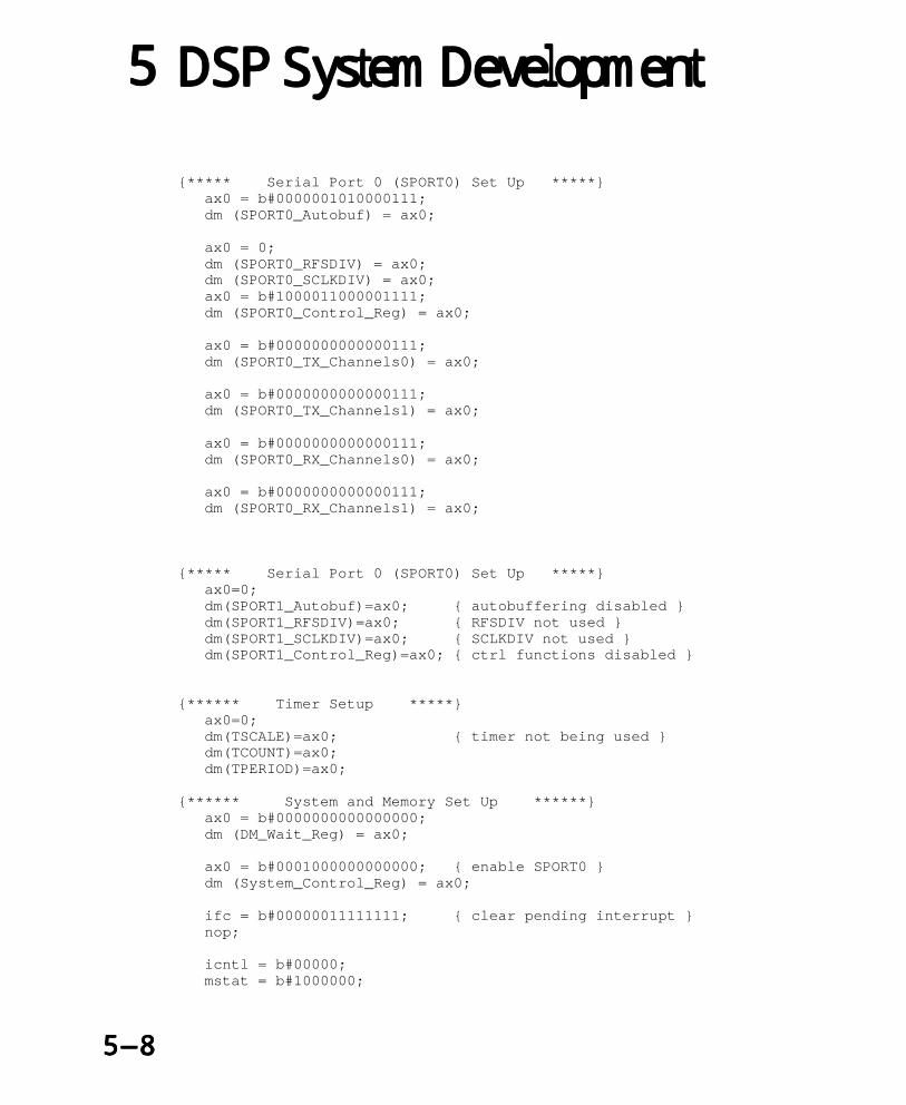
***** Serial Port 0 (SPORT0) Set Up ***** ax0 = b#0000001010000111;
dm (SPORT0_Autobuf) = ax0;
ax0 = 0;dm (SPORT0_RFSDIV) = ax0;dm (SPORT0_SCLKDIV) = ax0;ax0 = b#1000011000001111;dm (SPORT0_Control_Reg) = ax0;
ax0 = b#0000000000000111;dm (SPORT0_TX_Channels0) = ax0;
ax0 = b#0000000000000111;dm (SPORT0_TX_Channels1) = ax0;
ax0 = b#0000000000000111;dm (SPORT0_RX_Channels0) = ax0;
ax0 = b#0000000000000111;dm (SPORT0_RX_Channels1) = ax0;
***** Serial Port 0 (SPORT0) Set Up *****ax0=0;dm(SPORT1_Autobuf)=ax0; autobuffering disabled dm(SPORT1_RFSDIV)=ax0; RFSDIV not used dm(SPORT1_SCLKDIV)=ax0; SCLKDIV not used dm(SPORT1_Control_Reg)=ax0; ctrl functions disabled
****** Timer Setup *****ax0=0;dm(TSCALE)=ax0; timer not being used dm(TCOUNT)=ax0;dm(TPERIOD)=ax0;
****** System and Memory Set Up ******ax0 = b#0000000000000000;dm (DM_Wait_Reg) = ax0;
ax0 = b#0001000000000000; enable SPORT0 dm (System_Control_Reg) = ax0;
ifc = b#00000011111111; clear pending interrupt nop;
icntl = b#00000;mstat = b#1000000;

55555DSP System DevelopmentDSP System DevelopmentDSP System DevelopmentDSP System DevelopmentDSP System Development
5 – 95 – 95 – 95 – 95 – 9
***** AD1847 Codec intialization *******
ax0 = 1; dm(stat_flag) = ax0; clear flag imask = b#0001000000; enable transmit interrupt ax0 = dm (i1, m1); start interrupt tx0 = ax0;
check_init: ax0 = dm (stat_flag); wait for entire init af = pass ax0; buffer to be sent to if ne jump check_init; the codec
ay0 = 2;
check_acih: ax0 = dm (rx_buf); once initialized, wait ar = ax0 and ay0; for codec to come out if eq jump check_acih; of autocalibration
check_acil: ax0 = dm (rx_buf); once initialized, wait ar = ax0 and ay0; for codec to come out if ne jump check_acil; of autocalibration
idle;
ay0 = 0xbf3f; unmute left DAC ax0 = dm (init_cmds + 6); ar = ax0 AND ay0; dm (tx_buf) = ar; idle;
ax0 = dm (init_cmds + 7); unmute right DAC ar = ax0 AND ay0; dm (tx_buf) = ar; idle;
ax0 = 0xc901; clear autocalibration request dm (tx_buf) = ax0; idle; ax1 = 0x8000; control word to clear over-range flags dm (tx_buf) = ax1;
ifc = b#00000011111111; clear any pending interrupt nop;
imask = b#0000100000; enable rx0 interrupt
(listing continues on next page)

55555 DSP System DevelopmentDSP System DevelopmentDSP System DevelopmentDSP System DevelopmentDSP System Development
5 – 105 – 105 – 105 – 105 – 10
***** wait for interrupt and loop forever *****
talkthru: idle; jump talkthru;
****** Interrupt service routines *******
***** receive interrupt used for loopback *****input_samples: ena sec_reg; use shadow register bank
ax1 = dm (rx_buf + 1); get data from codec mx1 = dm (rx_buf + 2);
***** Put your code here to process samples received from CODEC. Left channel data is in register ax1 and right channel data is in register mx1. ********
dm (tx_buf + 1) = ax1; send data to codec dm (tx_buf + 2) = mx1;
rti;
***** transmit interrupt used for Codec initialization *****next_cmd: ena sec_reg; ax0 = dm (i3, m1); fetch next control word and dm (tx_buf) = ax0; place in transmit slot 0 ax0 = i3; ay0 = ^init_cmds; ar = ax0 - ay0; if gt rti; rti if more control words ax0 = 0x8000; else set done flag and dm (tx_buf) = ax0; remove MCE if done with init ax0 = 0; dm (stat_flag) = ax0; reset status flag rti;
.endmod;

55555DSP System DevelopmentDSP System DevelopmentDSP System DevelopmentDSP System DevelopmentDSP System Development
5 – 115 – 115 – 115 – 115 – 11
Step 6: Running The AssemblerStep 6: Running The AssemblerStep 6: Running The AssemblerStep 6: Running The AssemblerStep 6: Running The AssemblerAfter you have finished creating the text file which contains theassembly language program, you can run the assembler with thefollowing command.
asm21 my_prog -2181
In this example, the text file I created is named my_prog.dsp . The-2181 switch tells the assembler to accept ADSP-2181 specificinstructions. The assembler creates the appropriate object code file orfiles. There are a number of assembler switches that can be optionallyused for functions like list file creation, case sensitivity and object filenaming. Here is another example which specifies the creation of alisting file which will be called my_prog.lst .
asm21 my_prog -2181 -l
If you type the command asm21 followed by a carriage return (noarguments used), the proper use of the command and all the switcheswill be listed on the screen. The assembler creates an object file withthe extension .obj on the file name. The example command shownabove creates the file my_prog.obj .
Step 7: Running The LinkerStep 7: Running The LinkerStep 7: Running The LinkerStep 7: Running The LinkerStep 7: Running The LinkerThe linker creates an executable file from the object modules createdby the assembler. The following example creates a file calleddemo.exe .
ld21 my_prog -a adsp2181 -e demo
The architecture description file adsp2181.ach is specified with the-a switch and the executable file name is specified as demo.exewith the -e switch. There are a number of other switches that areused to create a symbol table, create a map file and specify the objectfiles indirectly (specify a file name where the file contains a list of allthe .obj files to be linked). If you type the command ld21followed by a carriage return (no arguments used), the proper use ofthe command and all the switches will be listed on the screen.
55555 DSP System DevelopmentDSP System DevelopmentDSP System DevelopmentDSP System DevelopmentDSP System Development
5 – 125 – 125 – 125 – 125 – 12
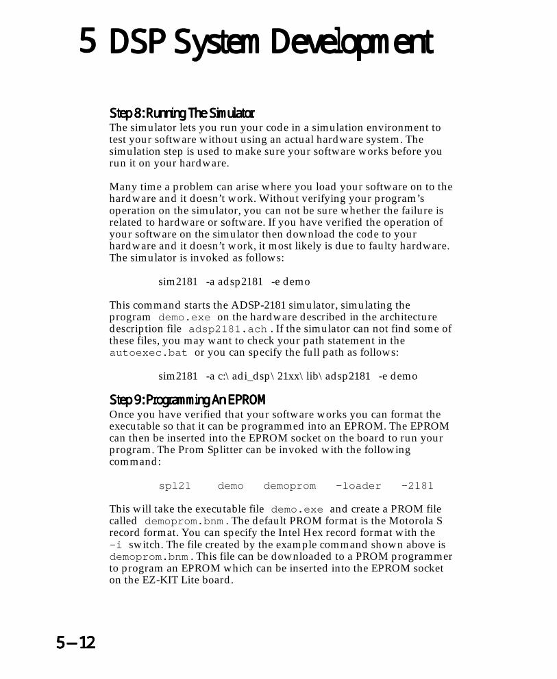
Step 8: Running The SimulatorStep 8: Running The SimulatorStep 8: Running The SimulatorStep 8: Running The SimulatorStep 8: Running The SimulatorThe simulator lets you run your code in a simulation environment totest your software without using an actual hardware system. Thesimulation step is used to make sure your software works before yourun it on your hardware.
Many time a problem can arise where you load your software on to thehardware and it doesn’t work. Without verifying your program’soperation on the simulator, you can not be sure whether the failure isrelated to hardware or software. If you have verified the operation ofyour software on the simulator then download the code to yourhardware and it doesn’t work, it most likely is due to faulty hardware.The simulator is invoked as follows:
sim2181 -a adsp2181 -e demo
This command starts the ADSP-2181 simulator, simulating theprogram demo.exe on the hardware described in the architecturedescription file adsp2181.ach . If the simulator can not find some ofthese files, you may want to check your path statement in theautoexec.bat or you can specify the full path as follows:
sim2181 -a c:\adi_dsp\21xx\lib\adsp2181 -e demo
Step 9: Programming An EPROMStep 9: Programming An EPROMStep 9: Programming An EPROMStep 9: Programming An EPROMStep 9: Programming An EPROMOnce you have verified that your software works you can format theexecutable so that it can be programmed into an EPROM. The EPROMcan then be inserted into the EPROM socket on the board to run yourprogram. The Prom Splitter can be invoked with the followingcommand:
spl21 demo demoprom -loader -2181
This will take the executable file demo.exe and create a PROM filecalled demoprom.bnm . The default PROM format is the Motorola Srecord format. You can specify the Intel Hex record format with the-i switch. The file created by the example command shown above isdemoprom.bnm . This file can be downloaded to a PROM programmerto program an EPROM which can be inserted into the EPROM socketon the EZ-KIT Lite board.

55555DSP System DevelopmentDSP System DevelopmentDSP System DevelopmentDSP System DevelopmentDSP System Development
5 – 135 – 135 – 135 – 135 – 13
Upon power up reset or when you hit the reset button on the board,the contents of the EPROM is automatically loaded into the internalprogram and data memories of the ADSP-2181 and coded executionbegins.
Step 10: Running The ADSP-2181 EZ-KIT Lite BoardStep 10: Running The ADSP-2181 EZ-KIT Lite BoardStep 10: Running The ADSP-2181 EZ-KIT Lite BoardStep 10: Running The ADSP-2181 EZ-KIT Lite BoardStep 10: Running The ADSP-2181 EZ-KIT Lite BoardThe EZ-KIT Lite board has an EPROM on it which contains ADSP-2181code. When the board is powered up (or reset) the code isautomatically transferred from the EPROM into the internal memoryof the ADSP-2181. The code shipped with the EZ-KIT Lite includes amonitor program which allows the ADSP-2181 to communicate withthe RS-232 interface. The code performs a self test and then sends anaudio signal to the audio output connector. You will need to have a setof powered speakers attached to the audio output connector to hearthe sound produced. The signal at this connector is a line level so youwill need a set of speakers that have an amplifier in them such as themodel CS-180 from Labtec.
Once you install the host software onto your PC you should be able torun the host program under Windows. You can then down load anexecutable file (.exe file produced by the linker). You should refer tothe sections of this manual that describe installation in more detail.
If you prefer, you can program your own EPROM and insert it into theEPROM socket on the EZ-KIT Lite board to run your own program instand alone mode.
Step 11: DebuggingStep 11: DebuggingStep 11: DebuggingStep 11: DebuggingStep 11: DebuggingIn general, if your EZ-KIT Lite board is not operating properly withthe programs provided there is probably a problem with the powerconnection, the connection to the host PC via the RS-232 cable, or aproblem with the components on the board. In general make sure thatall connections are made tightly and that the power supply voltage isin the proper range (8 VDC to 10 VDC). Also make sure that theEPROM is seated properly in the socket. Finally, make sure that noobjects are resting on the board or beneath the board causing a shortcircuit. When in doubt, press the reset button.
In general, if the software you develop does not work you shouldsimulate it to try to find the problem. There are a number of exampleprograms shipped with the EZ-KIT Lite. Use these as a basis to createyour own programs. More detail on debugging is found throughoutthis manual.

66666
6 – 16 – 16 – 16 – 16 – 1
EZ-KIT Lite Host ProgramEZ-KIT Lite Host ProgramEZ-KIT Lite Host ProgramEZ-KIT Lite Host ProgramEZ-KIT Lite Host Program
PROGRAM OVERVIEWPROGRAM OVERVIEWPROGRAM OVERVIEWPROGRAM OVERVIEWPROGRAM OVERVIEWThe EZ-KIT Lite Host Program is a Windows-based applicationprogram following standard Windows Graphical User Interfaceconventions. This is the application program you use to communicatewith the EZ-LAB board. With it you can run EZ-KIT Litedemonstration programs, upload/download program and datamemory contents, download user DSP programs, and execute userDSP programs. The following screen shows the main menu of the HostProgram.

66666 EZ-KIT Lite Host ProgramEZ-KIT Lite Host ProgramEZ-KIT Lite Host ProgramEZ-KIT Lite Host ProgramEZ-KIT Lite Host Program
6 – 26 – 26 – 26 – 26 – 2
COMMAND SUMMARYCOMMAND SUMMARYCOMMAND SUMMARYCOMMAND SUMMARYCOMMAND SUMMARYBy pointing and clicking on menu items, you can select from the manycommands available. This chapter describes in detail each of thesecommands. The following commands are available.
- DTMFrun the DTMF demonstration program
- Filteringrun the filtering demonstration program
- Echo Cancellationrun the echo cancellation demonstration program
- Speech Compressionrun the LPC and ADPCM speech compression demonstrationprograms
- Download DSP program & Godownload user programs and begin execution
- Download DSP programdownload user programs but do not start execution, alsodownload memory image files
- Gobegin execution from a given address
- Upload data memoryupload a block of memory into a memory image file
- Upload program memoryupload a block of memory into a memory image file
- Download data memorydownload a data memory image file to a given address
- Download program memorydownload a program memory image file to a given address
- AboutThe last line in the dialog box indicates whether serialcommunication is established.

66666EZ-KIT Lite Host ProgramEZ-KIT Lite Host ProgramEZ-KIT Lite Host ProgramEZ-KIT Lite Host ProgramEZ-KIT Lite Host Program
6 – 36 – 36 – 36 – 36 – 3
DETAILED COMMANDSDETAILED COMMANDSDETAILED COMMANDSDETAILED COMMANDSDETAILED COMMANDSAll commands are available via the standard menu bar selections andtheir drop-down menu items. You will notice that in addition to thestandard Windows menu bar selections such as ‘File’ and ‘Help,’ thereare some EZ-KIT Lite related items. All menu options are described indetail in the following sections.
File MenuFile MenuFile MenuFile MenuFile MenuSince no information is retained in memory, the standard file save and fileopen commands are not applicable. There is only one command under the‘File’ heading.
- ExitMake this selection if you want to exit the EZ-KIT Host Program.

66666 EZ-KIT Lite Host ProgramEZ-KIT Lite Host ProgramEZ-KIT Lite Host ProgramEZ-KIT Lite Host ProgramEZ-KIT Lite Host Program
6 – 46 – 46 – 46 – 46 – 4
View MenuView MenuView MenuView MenuView MenuThe View menu deals with the Toolbar and the Status Bar.
ToolbarToolbarToolbarToolbarToolbarSelection of this feature will remove the check mark and remove theToolbar near the top of the main window. Repeat to replace the checkmark and bring back the Toolbar.
Toolbar is the gray bar immediately below the menu bar with severalsmall square buttons on the left hand side. These buttons providealternate quick access to useful commands. Simply click on these buttonswith a mouse instead of selecting the drop down menu and select thecorresponding menu items. A description follows.
- Download user program & GoIt is the first button from the left with the symbol of an opened folder. Thisbutton selects the corresponding menu selection under ‘Loading’ menu. Itwill download a user program and start user program execution. Select anADSP-2181 executable file with a .exe extension. This is an executable filethat is created by the ADSP-2181 linker.
- About EzkitAppIt is the second button from the left with a question mark. This buttonselects the corresponding menu selection under ‘Help’ menu. It displaysthe About dialog box.

66666EZ-KIT Lite Host ProgramEZ-KIT Lite Host ProgramEZ-KIT Lite Host ProgramEZ-KIT Lite Host ProgramEZ-KIT Lite Host Program
6 – 56 – 56 – 56 – 56 – 5
The useful item in the About dialog box is the last line in the dialog box. Ifthe Host Program is able to communicate with the EZ-KIT monitorprogram the last line will read ‘EZ-KIT monitor is alive and well.’Otherwise the line will read ‘EZ-KIT monitor is not running; try reset.’You may try to push the reset button on the EZ-KIT Lite board to re-activate the resident monitor.
- Download program memoryIt is the third button from the left with the letter ‘P’ and a downwardpointing arrow. This button selects the corresponding menu selectionunder ‘Loading’ menu. It will download a program memory image from afile to the DSP program memory at the specified starting address. You willneed to select the Go command to run the program. Please see thecorresponding section under ‘Loading’ menu for more detail.
- Download data memoryIt is the fourth button from the left with the letter ‘D’ and a downwardpointing arrow. This button selects the corresponding menu selectionunder ‘Loading’ menu. It will download a data memory image from a fileto the DSP data memory starting from a user specified memory location.Please see the corresponding section under ‘Loading’ menu for moredetail.
- Upload program memoryIt is the fifth button from the left with the letter ‘P’ and a upward pointingarrow. This button selects the corresponding menu selection under‘Loading’ menu. It will upload a program memory image from the DSPprogram memory to a file. You specify the specified starting address andthe number of program memory locations to be transferred. Please see thecorresponding section under ‘Loading’ menu for more detail.
- Upload data memoryIt is the sixth button from the left with the letter ‘D’ and a upwardpointing arrow. This button selects the corresponding menu selectionunder ‘Loading’ menu. It will upload a data memory image from the DSPdata memory to a file. You specify the specified starting address and thenumber of data memory locations to be transferred. Please see thecorresponding section under ‘Loading’ menu for more detail.

66666 EZ-KIT Lite Host ProgramEZ-KIT Lite Host ProgramEZ-KIT Lite Host ProgramEZ-KIT Lite Host ProgramEZ-KIT Lite Host Program
6 – 66 – 66 – 66 – 66 – 6
Status BarStatus BarStatus BarStatus BarStatus BarSelection of this option will remove the check mark and remove the StatusBar near the bottom of the main window. Repeat to replace the checkmark and bring back the Status Bar.
When a menu bar selection is highlighted, a more detailed description ofthe currently highlighted menu selection is given in the Status Bar.
Demo MenuDemo MenuDemo MenuDemo MenuDemo MenuFrom the menu options, select one of the available demonstrationprograms to run on the EZ-KIT Lite. These demos may also be selecteddirectly from the floating buttons. Please refer to the correspondingsection for more detailed information.
DTMFDTMFDTMFDTMFDTMFSelects the DTMF DSP demo program. This demonstration generatesDual-Tone Multi-Frequency (DTMF) tones, as used in the telephonenetwork for push-button signaling. A DTMF tone is composed of twodifferent single frequency tones - one of four row tones added to one offour column tones. Thus, a full implementation of a DTMF standard tonegenerator can generate 16 different tones (only 12 are commonly used onconsumer handsets).

66666EZ-KIT Lite Host ProgramEZ-KIT Lite Host ProgramEZ-KIT Lite Host ProgramEZ-KIT Lite Host ProgramEZ-KIT Lite Host Program
6 – 76 – 76 – 76 – 76 – 7
When selected the Windows Application Interface will download thenecessary DSP program to the EZ-KIT LITE resulting in the followingdialog box.
When it outputs a DTMF tone, EZ-KIT generates the two requisite sinewaves, scales them and adds them, and then outputs the result to thecodec for conversion to an analog signal. At the start of this program,EZ-KIT generates a dial tone to the output speaker. The followingselections are possible.
- Generate dial toneThis selection may be selected by clicking the corresponding radio buttonor typing the letter ‘t.’ A standard dial tone which is a sum of continuoussine waves is generated.
- Generate DTMF digitsThis option may be selected by clicking the corresponding radio button ortyping the letter ‘d.’ The phone number of an Analog Devices DSPapplications engineer is programmed into the demo program. Make thisselection to generate the phone number. If you hold an off-hook telephonehandset to the output speaker, the DTMF tones will tell the network callswitching apparatus to connect you to the applications engineer. Do thisonly if you want to make a call.
- CloseThis option terminates the demonstration program and restores theEZ-KIT resident monitor program before returning the user to the topmenu bar selection. This allows a new demonstration to be selected.

66666 EZ-KIT Lite Host ProgramEZ-KIT Lite Host ProgramEZ-KIT Lite Host ProgramEZ-KIT Lite Host ProgramEZ-KIT Lite Host Program
6 – 86 – 86 – 86 – 86 – 8
FilteringFilteringFilteringFilteringFilteringSelects the FIR Filtering DSP demo program. This program demonstratesthe effect of four bandpass filters against no filter on microphone input oran internally generated noise source.
When selected the Windows Application Interface will download thenecessary DSP program to the EZ-KIT Lite and display the followingdialog box.
This demonstration starts with a talk-through program. The AD1847codec digitizes the analog microphone input and transmits the data to theDSP’s serial port. The DSP reads data from the serial port and retransmitsthe data back to the codec. The codec converts the data to an analog signalthat drives the speaker. No digital processing is performed on the data.When you speak into the microphone, you should hear your voicethrough the speaker.
The top row radio buttons use voice input from the microphone.
The filters have equivalent bandwidth and are evenly spaced on alogarithmic frequency axis. All FIR filters are 256 taps, and have beendesigned for 0.1 ripple.FIR Filter Lower Stop Band Pass band Upper Stop BandFIR Filter Lower Stop Band Pass Band Upper Stop Band
FIR1 0 - 269 Hz 328 - 448 Hz 547 - 4000 HzFIR2 0 - 426 Hz 521 - 710 Hz 866 - 4000 HzFIR3 0 - 675 Hz 825 - 1125 Hz 1375 - 4000 HzFIR4 0 - 1070 Hz 1308 - 1783 Hz 2179 - 4000 Hz
The bottom rows radio buttons use random noise as inputs.

66666EZ-KIT Lite Host ProgramEZ-KIT Lite Host ProgramEZ-KIT Lite Host ProgramEZ-KIT Lite Host ProgramEZ-KIT Lite Host Program
6 – 96 – 96 – 96 – 96 – 9
- CloseThis option terminates the demonstration program and restores theEZ-KIT resident monitor program before returning the user to the topmenu bar selection. This allows a new demonstration to be selected.
Echo CancellationEcho CancellationEcho CancellationEcho CancellationEcho CancellationSelects the Echo Canceller DSP demo program. This programdemonstrates echo cancellation on a simulated echoing channel.
The AD1847 codec digitizes the analog microphone input and transmitsthe data to the DSP’s serial port. The DSP internally generates an echoedsignal by summing the serial input with the output of a simulated echochannel. The echo channel consists of a linear delay implemented as along FIR filter with zero-value tap weights and a 16-tap dispersive FIRfilter. The echo canceled output is sent to the codec for reconstruction.
When selected the Windows Application Interface will download thenecessary DSP program to the EZ-KIT Lite resulting in the followingdialog box.
Initially the program sends the echoed output to the codec without echocancellation. The following selections are possible.
- NextWhen this button is depressed for the first time the program enters echocancellation mode. The dialog box shown on the following page. Therewill be a significant reduction in echo. Further depression of the buttonwill change the position of the dispersive filter and will force the filter toadapt to a new echo path.

66666 EZ-KIT Lite Host ProgramEZ-KIT Lite Host ProgramEZ-KIT Lite Host ProgramEZ-KIT Lite Host ProgramEZ-KIT Lite Host Program
6 – 106 – 106 – 106 – 106 – 10
- CloseThis option terminates the demonstration program and restores theEZ-KIT resident monitor program before returning the user to the topmenu bar selection. This allows a new demonstration to be selected.
ADPCMADPCMADPCMADPCMADPCMSelects the ADPCM DSP demo program. This program demonstratesAdaptive Differential Pulse Code Modulation (ADPCM) capabilities.ADPCM consists of a number of real-time speech compression algorithms.For each sampling period it employs a linear predictive filter to generate apredicted output. The difference between the predicted output and actualsampled value is sent through the communication channel. Since thedynamic range of the differential error is significantly lower than thedynamic range of the voice signal, a lower bit rate results.
When selected the Windows Application Interface will download thenecessary DSP program to the EZ-KIT Lite resulting in the followingdialog box.
Initially the digitized microphone samples from the codec are sent directlyto the codec for reconstruction. The following selections are possible.

66666EZ-KIT Lite Host ProgramEZ-KIT Lite Host ProgramEZ-KIT Lite Host ProgramEZ-KIT Lite Host ProgramEZ-KIT Lite Host Program
6 – 116 – 116 – 116 – 116 – 11
- ADPCM codingThis option enables the ADPCM encoding/decoding feature. Eachdigitized microphone sample from the codec is first encoded and thendecoded using ADPCM. After it is decoded, it is sent back to the codec forreconstruction. The red LED will light up when ADPCM encoding is ineffect.
- Straight throughThis option enables the straight through. The digitized microphonesamples from the codec are sent directly back to the codec forreconstruction. The red LED will be off when straight through is in effect.
- CloseThis option terminates the demonstration program and restores theEZ-KIT resident monitor program before returning the user to the topmenu bar selection. This allows a new demonstration to be selected.
7.8k LPC7.8k LPC7.8k LPC7.8k LPC7.8k LPCSelects the 7.8k LPC DSP demo program.
- Interrupt button on EZ-KIT LitePush the Interrupt button on EZ-KIT Lite to toggle between talk throughand 7.8k LPC encoding. The red LED will light up when LPC encoding isin effect.
- CloseThis option terminates the demonstration program and restores theEZ-KIT resident monitor program before returning the user to the topmenu bar selection. This allows new a demonstration to be selected.

66666 EZ-KIT Lite Host ProgramEZ-KIT Lite Host ProgramEZ-KIT Lite Host ProgramEZ-KIT Lite Host ProgramEZ-KIT Lite Host Program
6 – 126 – 126 – 126 – 126 – 12
2.4k LPC2.4k LPC2.4k LPC2.4k LPC2.4k LPCSelects the 2.4k LPC DSP demo program.
- Interrupt button on EZ-KIT LitePush the Interrupt button on EZ-KIT Lite to toggle between talk throughand 2.4k LPC encoding. The red LED will light up when LPC encoding isin effect.
- CloseThis option terminates the demonstration program and restores theEZ-KIT resident monitor program before returning the user to the topmenu bar selection. This allows a new demonstration to be selected.
Floating MenuFloating MenuFloating MenuFloating MenuFloating MenuAlternatively all the demo programs can be selected by clicking thecorresponding buttons in the following floating dialog box. This dialogbox may be turned on or off via the options menu described later.
66666EZ-KIT Lite Host ProgramEZ-KIT Lite Host ProgramEZ-KIT Lite Host ProgramEZ-KIT Lite Host ProgramEZ-KIT Lite Host Program
6 – 136 – 136 – 136 – 136 – 13
The extra button at the bottom of the dialog box provides an alternativeand quick way of exiting the Window Application Interface program.
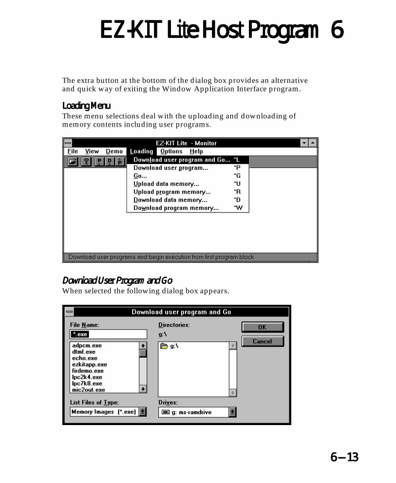
Loading MenuLoading MenuLoading MenuLoading MenuLoading MenuThese menu selections deal with the uploading and downloading ofmemory contents including user programs.
Download User Program and GoDownload User Program and GoDownload User Program and GoDownload User Program and GoDownload User Program and GoWhen selected the following dialog box appears.

66666 EZ-KIT Lite Host ProgramEZ-KIT Lite Host ProgramEZ-KIT Lite Host ProgramEZ-KIT Lite Host ProgramEZ-KIT Lite Host Program
6 – 146 – 146 – 146 – 146 – 14
Selects a memory image file (*.exe) for downloading. Program memoryand data memory images will be downloaded to locations specified in thememory image file kernel in the corresponding memory space. Themonitor then transfers DSP execution to the newly downloaded program.
All user interrupt vectors will be directed to a special temporary buffer toenable the monitor to function. When the monitor is finally issued acommand to execute user program, the redirected user interrupt vectorswill be copied from the temporary buffer to the intended locations.
Interrupts are disabled before entering the user program. All userinterrupts are masked using the DIS INTS instruction. The mask is also setto 0 and the timer is disabled.
The first location of the program memory image kernel encountered in thememory image file is used as the entry point to the user program. Themonitor performs a subroutine call to that location. The user programshould execute an RTS instruction to return to the monitor. Upon re-entering the monitor program all interrupt vectors are restored to thecontents prior to the user program being downloaded to enable themonitor to continue to function. Alternatively, the user can set up theBDMA to simulate a power up BDMA boot load thus reloading themonitor program from the EPROM.
The monitor reserves certain memory locations. The user program shouldnot use these monitor reserved memory locations. Please refer to chapterdescribing the EZ-KIT Lite Monitor Program for more details on reservedmemory.

66666EZ-KIT Lite Host ProgramEZ-KIT Lite Host ProgramEZ-KIT Lite Host ProgramEZ-KIT Lite Host ProgramEZ-KIT Lite Host Program
6 – 156 – 156 – 156 – 156 – 15
Download User ProgramDownload User ProgramDownload User ProgramDownload User ProgramDownload User ProgramWhen selected the following dialog box appears.
Selects a memory image file (*.exe) file for downloading. The differencebetween this option and the previous one is that this selection does nottransfer DSP execution to the downloaded program upon downloadcompletion.
Upon download completion the monitor will continue to function. Theprogram's entry point is reported in the acknowledgment dialog box. Userprogram execution may be started by using the ‘Go’ command, describedimmediately below.
For all other details please refer to the previous section for ‘Downloaduser program and Go.’
GoGoGoGoGoWhen selected the following dialog box appears.

66666 EZ-KIT Lite Host ProgramEZ-KIT Lite Host ProgramEZ-KIT Lite Host ProgramEZ-KIT Lite Host ProgramEZ-KIT Lite Host Program
6 – 166 – 166 – 166 – 166 – 16
Enter a hexadecimal address as the starting address of user programs.Valid address range is from 0x0000 to 0x37ff inclusive. Program memorylocations 0x3800 to 0x3fff are used to store the monitor code. Loading intothese locations will corrupt the monitor. For more details on user programrestrictions please refer to the reference manual for EZ-KIT Lite.
Upload Data MemoryUpload Data MemoryUpload Data MemoryUpload Data MemoryUpload Data MemoryWhen selected the following dialog box appears.
This command uploads a block of DSP program memory content to amemory image (*.exe) file on the host computer. Specify in hexadecimalthe starting address and number of words. The resulting file may bedownloaded back into the program memory at any specified non-restricted location. The file may also be examined by using any text editor.
You will get an error message if you entered an invalid hexadecimalnumber or specified an invalid range of memory, e.g. starting addressplus number of words exceeds the memory range.

66666EZ-KIT Lite Host ProgramEZ-KIT Lite Host ProgramEZ-KIT Lite Host ProgramEZ-KIT Lite Host ProgramEZ-KIT Lite Host Program
6 – 176 – 176 – 176 – 176 – 17
Upload Program MemoryUpload Program MemoryUpload Program MemoryUpload Program MemoryUpload Program MemoryWhen selected the following dialog box appears.
This command uploads a block of DSP data memory content to a memoryimage (*.exe) file on the host computer. Specify in hexadecimal thestarting address and number of words. The resulting file may bedownloaded back into the program memory at any specified non-restricted location. The file may also be examined by using any text editor.
You will get an error message if you entered an invalid hexadecimalnumber or specified an invalid range of memory, e.g. starting addressplus number of words goes beyond the end of memory.

66666 EZ-KIT Lite Host ProgramEZ-KIT Lite Host ProgramEZ-KIT Lite Host ProgramEZ-KIT Lite Host ProgramEZ-KIT Lite Host Program
6 – 186 – 186 – 186 – 186 – 18
Download Data MemoryDownload Data MemoryDownload Data MemoryDownload Data MemoryDownload Data MemoryWhen selected the following dialog box appears.
This command downloads a memory image (*.exe) file from the hostcomputer into DSP data memory starting from the specified hexadecimalstart address.
The first data memory image kernel in the image file will be downloaded.The memory image file may be memory image file generated (uploaded)by the Host Program or generated by the ADSP-21xx Linker. Since theHost Program generated file will have only one corresponding memorykernel, the entire file content will be downloaded. The linker generatedimage file may have multiple program memory and data memory kernels.Only the first data memory kernel will be downloaded and the rest will beignored.
Since the memory image file format is an ASCII text file with no checksuminformation, it is possible to use an ASCII text editor to edit the memoryimage file and alter, delete, or add entries. Please refer to the ADSP-2100Family Assembler & Simulator Manual for the format definition.However, as the format is rather straight forward, with a little inspectionand experimentation you may be able to do the modification withoutreferring to the manual.

66666EZ-KIT Lite Host ProgramEZ-KIT Lite Host ProgramEZ-KIT Lite Host ProgramEZ-KIT Lite Host ProgramEZ-KIT Lite Host Program
6 – 196 – 196 – 196 – 196 – 19
You will get an error message if you entered an invalid hexadecimalnumber or specified an invalid range of memory, e.g. starting addressplus number of words goes beyond the end of memory.
DO NOT overwrite the monitor reserved memory locations.
Download Program MemoryDownload Program MemoryDownload Program MemoryDownload Program MemoryDownload Program MemoryWhen selected the following dialog box appears.
This command downloads a memory image (*.exe) file from the hostcomputer into DSP program memory starting from the specifiedhexadecimal start address.
The first program memory image kernel in the image file will bedownloaded. The memory image file may be memory image filegenerated (uploaded) by the Host Program or generated by the ADSP-21xx Linker. Since the Host Program generated file will have only onecorresponding memory kernel, the entire file content will be downloaded.The linker generated image file may have multiple program memory anddata memory kernels. Only the first program memory kernel will bedownloaded and the rest will be ignored.

66666 EZ-KIT Lite Host ProgramEZ-KIT Lite Host ProgramEZ-KIT Lite Host ProgramEZ-KIT Lite Host ProgramEZ-KIT Lite Host Program
6 – 206 – 206 – 206 – 206 – 20
Since the memory image file format is an ASCII text file with no checksuminformation, it is possible to use an ASCII text editor to edit the memoryimage file and alter, delete, or add entries. Please refer to the Cross-Software Manual for the format definition. However, as the format is ratherstraight forward, with a little inspection and experimentation you may beable to do the modification without referring to the manual.
You will get an error message if you entered an invalid hexadecimalnumber or specified an invalid range of memory, e.g. starting addressplus number of words goes beyond the end of memory.
DO NOT overwrite the monitor reserved memory locations.
Options MenuOptions MenuOptions MenuOptions MenuOptions MenuThese selections determine the operation of the Host Program.

66666EZ-KIT Lite Host ProgramEZ-KIT Lite Host ProgramEZ-KIT Lite Host ProgramEZ-KIT Lite Host ProgramEZ-KIT Lite Host Program
6 – 216 – 216 – 216 – 216 – 21
SettingsSettingsSettingsSettingsSettingsWhen selected the following dialog box appears.
Please select the corresponding serial communication port to which theEZ-KIT Lite board is connected. This selection is saved in theconfiguration file ‘ezkitapp.ini.’ However, it is not critical to have the‘ezkitapp.ini’ file available; if the Host Program did not find theconfiguration file it will bring this dialog box up to allow the user to makea selection.
List Of DemosList Of DemosList Of DemosList Of DemosList Of DemosWhen selected, the following dialog box appears.

66666 EZ-KIT Lite Host ProgramEZ-KIT Lite Host ProgramEZ-KIT Lite Host ProgramEZ-KIT Lite Host ProgramEZ-KIT Lite Host Program
6 – 226 – 226 – 226 – 226 – 22
Help MenuHelp MenuHelp MenuHelp MenuHelp Menu
About EZ-KITAbout EZ-KITAbout EZ-KITAbout EZ-KITAbout EZ-KITWhen selected the following dialog box appears.
The third line will indicate whether the Host Program could communicatewith the resident monitor. The line ‘EZ-KIT monitor is alive and well’ isdisplayed if the host to monitor communication is functioning; otherwisethe line ‘EZ-KIT monitor is not running; try reset’ is displayed. Click ‘OK’to remove the dialog box.
User Configurable SettingsUser Configurable SettingsUser Configurable SettingsUser Configurable SettingsUser Configurable SettingsSeveral operating aspects of the Host Program can be customized bychanging the initialization string in ‘EzkitApp.ini.’ Two of these areautomatically managed by the Host Program. The only one that may needto be manually modified is the time-out duration for the dialog box. The‘EzkitApp.ini’ is not critical to the functioning of the Host Program. If thefile is not found the Host Program simply uses default settings andprompts the user for the correct serial communication port number.Details follow.

66666EZ-KIT Lite Host ProgramEZ-KIT Lite Host ProgramEZ-KIT Lite Host ProgramEZ-KIT Lite Host ProgramEZ-KIT Lite Host Program
6 – 236 – 236 – 236 – 236 – 23
• [EZ-KIT Interface App]This is the heading for the section and it should not be changed.
• PortNo=2This is the serial communication port number. It is managed by the HostProgram and should not be changed.
• MessageTimeOut=5This is the dialog box time out duration. The default value is five seconds.Setting it to zero will disable the automatic time out feature. This is theonly setting that may require direct user modification.
• ShowFloatingDialogBox=1This is the visibility of the floating dialog box. If this is 1 the floatingdialog will be visible when Host Program begins running. It is managedby the Host Program and should not be changed.
Error Messages & TroubleshootingError Messages & TroubleshootingError Messages & TroubleshootingError Messages & TroubleshootingError Messages & TroubleshootingSeveral error messages may be reported should there be any problemsencountered in communicating to the EZ-KIT Lite monitor program.These error messages are described below.
This indicates that the resident monitor detected the indicated errorduring its power up self test. Push the reset button on the EZ-KIT Liteboard and try again. A persistent problem may indicate the board isdefective.

66666 EZ-KIT Lite Host ProgramEZ-KIT Lite Host ProgramEZ-KIT Lite Host ProgramEZ-KIT Lite Host ProgramEZ-KIT Lite Host Program
6 – 246 – 246 – 246 – 246 – 24
This indicates that the Host Program has timed out waiting for themonitor to respond. A possible cause is that the monitor reserved memorylocations may have been corrupted. Push the reset button on the EZ-KITLite board and try again.
This indicates that the Windows Communication Module has reported anerror to the Host Program. A possible cause is conflict between Windowsapplications. Close all other programs and try again. It will also help toverify that the serial communication port selected is functioning bytemporarily reconfiguring the mouse driver to use this port.
This indicates that a checksum error has been detected. For all memorytransfers a checksum is computed for the block of memory content beingtransferred by both the monitor and the Host Program. A possible cause isexcessive line or environment noise. If the problem persists try shorteningthe length of the serial communication port cable. Also experiment withthe location of the EZ-KIT Lite board and your compter.

66666EZ-KIT Lite Host ProgramEZ-KIT Lite Host ProgramEZ-KIT Lite Host ProgramEZ-KIT Lite Host ProgramEZ-KIT Lite Host Program
6 – 256 – 256 – 256 – 256 – 25
This indicates that the Host Program is unable to ascertain the correctfunctioning of the EZ-KIT Lite resident monitor program. A possiblecause is that the Host Program encountered problem with the WindowsCommunication Module. Exit Windows and try again.
This is the catch-all error message. All other unknown errors result in thismessage. A possible cause may be missing demo program images files,corrupted files, and internal programming error.
This indicates the Host Program did not get a response from the monitorprogram. A possible cause is that the EZ-KIT Lite board is not connectedto the selected serial port, or that another Windows application is usingthe selected serial port. Close all other Windows applications and tryagain.
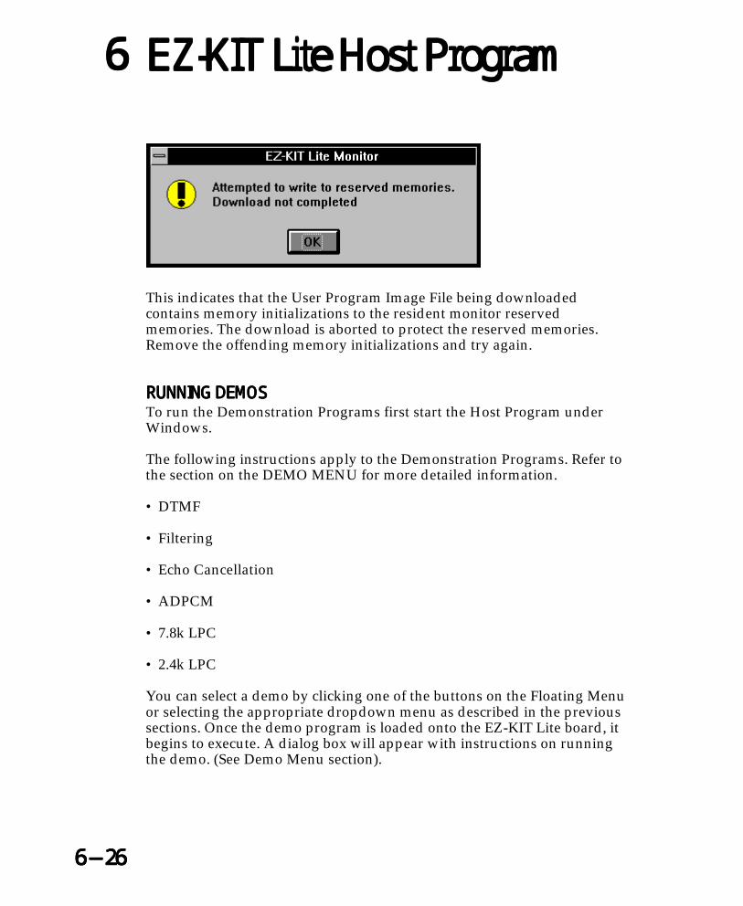
66666 EZ-KIT Lite Host ProgramEZ-KIT Lite Host ProgramEZ-KIT Lite Host ProgramEZ-KIT Lite Host ProgramEZ-KIT Lite Host Program
6 – 266 – 266 – 266 – 266 – 26
This indicates that the User Program Image File being downloadedcontains memory initializations to the resident monitor reservedmemories. The download is aborted to protect the reserved memories.Remove the offending memory initializations and try again.
RUNNING DEMOSRUNNING DEMOSRUNNING DEMOSRUNNING DEMOSRUNNING DEMOSTo run the Demonstration Programs first start the Host Program underWindows.
The following instructions apply to the Demonstration Programs. Refer tothe section on the DEMO MENU for more detailed information.
• DTMF
• Filtering
• Echo Cancellation
• ADPCM
• 7.8k LPC
• 2.4k LPC
You can select a demo by clicking one of the buttons on the Floating Menuor selecting the appropriate dropdown menu as described in the previoussections. Once the demo program is loaded onto the EZ-KIT Lite board, itbegins to execute. A dialog box will appear with instructions on runningthe demo. (See Demo Menu section).

66666EZ-KIT Lite Host ProgramEZ-KIT Lite Host ProgramEZ-KIT Lite Host ProgramEZ-KIT Lite Host ProgramEZ-KIT Lite Host Program
6 – 276 – 276 – 276 – 276 – 27
CREATING YOUR OWN PROGRAMSCREATING YOUR OWN PROGRAMSCREATING YOUR OWN PROGRAMSCREATING YOUR OWN PROGRAMSCREATING YOUR OWN PROGRAMSThe Host Program running on the PC communicates through the COMport to the EZ-KIT Lite board. The commands sent by the host software tothe EZ-KIT Lite board and the response received by the host are describedin this chapter. All values are in binary format. Use this information if youdesire to create your own Host Program. The following are the serialcommands that EZ-KIT Lite understands.
1. Beep sent: $$$ received: ok[led count][alive called count][selftest hi][selftest lo] [cmds4demo hi][cmds4demo lo]
[led count] is the lower 8 bits of a counter incremented at 28800 rate. [alive called count] is incremented by one each time alive is called. [selftest hi][selftest lo] is the selftest result [cmds4demo hi][cmds4demo lo] is demo command variable sing/generate 1 kHz tone.
2. Alive inquiry sent: $OK received: ok[led count][alive called count][selftest hi][selftest lo] [cmds4demo hi][cmds4demo lo]
[led count] is the lower 8 bits of a counter incremented at 28800 rate. [alive called count] is incremented by one each time alive is called. [selftest hi][selftest lo] is the selftest result [cmds4demo hi][cmds4demo lo] is demo command variable
3. upload DM sent: $UD[hi start][lo start][hi len][lo len] received: [hi][lo]...[hi sum][lo sum]
4. upload PM sent: $UP[hi start][lo start][hi len][lo len] received: [hi][mi][lo]...[hi sum][mi sum][lo sum]

66666 EZ-KIT Lite Host ProgramEZ-KIT Lite Host ProgramEZ-KIT Lite Host ProgramEZ-KIT Lite Host ProgramEZ-KIT Lite Host Program
6 – 286 – 286 – 286 – 286 – 28
5. download DM sent: $DD[hi start][lo start][hi len][lo len][hi][lo]... received: ![hi sum][lo sum]
6. download PM sent: $DP[hi start][lo start][hi len][lo len][hi][mi][lo]... received: ![hi sum][mi sum][lo sum]
7. Call subroutine sent: $GO[hi address][loaddress] received: ![hi address][loaddress]

77777
7 – 17 – 17 – 17 – 17 – 1
EZ-KIT Lite Monitor ProgramEZ-KIT Lite Monitor ProgramEZ-KIT Lite Monitor ProgramEZ-KIT Lite Monitor ProgramEZ-KIT Lite Monitor Program
PROGRAM OVERVIEWPROGRAM OVERVIEWPROGRAM OVERVIEWPROGRAM OVERVIEWPROGRAM OVERVIEWThe Monitor Program resides in an on-board EPROM. It is automaticallyloaded into the on-chip program and data memories at reset. As soon asthe monitor begins execution it performs a self test of DSP registers, on-chip memories, and a reset and initialization of AD1847 codec. It thenwaits for commands via the RS-232 serial communication port. A codectalk through routine is also running in an interrupt routine.
MONITOR FEATURESMONITOR FEATURESMONITOR FEATURESMONITOR FEATURESMONITOR FEATURESThis monitor has the following features.
• Power up self test• AD1847 codec initialization and talk through• 9600 bps UART emulation• upload and download of both program and data memory contents via
serial link
RESTRICTIONSRESTRICTIONSRESTRICTIONSRESTRICTIONSRESTRICTIONSIn order to facilitate the function of the monitor, certain restrictions areimposed on all user programs. These are hard restrictions becauseviolation will interfere with the proper downloading of the userprograms. These restrictions include the following.
• Reserved program memory 0x3800 to 0x3fffThis is where the monitor program resides. The user program shouldnot download into these locations. Any violation will destroy themonitor resulting in incomplete user program download.
• Reserved data memory 0x3e00 to 0x3fdfThese are the monitor operating variables. User programsdownloading into these locations will interfere with the monitorexecution resulting in an incomplete user program download.

77777 EZ-KIT Lite Monitor ProgramEZ-KIT Lite Monitor ProgramEZ-KIT Lite Monitor ProgramEZ-KIT Lite Monitor ProgramEZ-KIT Lite Monitor Program
7 – 27 – 27 – 27 – 27 – 2
• Returning to the monitorAfter the download of your program is complete, the monitor softwarecalls your code as a subroutine. Your code should end with an RTSinstruction to properly return to the monitor.
For user programs that do not return to the monitor there is norestriction imposed after the program has been downloaded. In otherwords, while the memory image file should not attempt to initializethe reserved memories, the user program is nevertheless free to usethese memories after its execution.
CREATING YOUR OWN PROGRAMS TO BE USED WITH THE MONITORCREATING YOUR OWN PROGRAMS TO BE USED WITH THE MONITORCREATING YOUR OWN PROGRAMS TO BE USED WITH THE MONITORCREATING YOUR OWN PROGRAMS TO BE USED WITH THE MONITORCREATING YOUR OWN PROGRAMS TO BE USED WITH THE MONITORYou can edit one of the example programs supplied or you can createyour own program using the development tools included in your EZ-KITLite. See chapter 5 for more information. There are a few things to notewhen developing programs that you want to run with the monitor.
User programs may use all non-reserved program memory and non-reserved data memory. These are locations 0x0000 to 0x37ff for programmemory and locations 0x0000 to 0x3dff for data memory.
• Program entry pointUser programs to be downloaded by the Host Program should havetheir entry point at the beginning of the first program memory kernel.This can be achieved by making the entry point the first instruction inthe module and specifying that module first during linking. In mostcases, your program will start at location 0x0000. You can use theassembler directive .module/ram/abs=0 to specify this (seeexamples).
• Interrupt enableAll interrupts are masked (by IMASK = 0.) before execution istransferred to the user programs. This is so that the user program cansafely carry out initializations before it re-enables interrupts.
• Interrupt vectorsThe user program must initialize all interrupt vectors it is using.Interrupt IRQ1 can not be used in your program since it is dedicated tothe RS232 communications. You can place "dummy" RTI instructionsin your code at this interrupt vector (location 0x0020 through 0x0023).

77777EZ-KIT Lite Monitor ProgramEZ-KIT Lite Monitor ProgramEZ-KIT Lite Monitor ProgramEZ-KIT Lite Monitor ProgramEZ-KIT Lite Monitor Program
7 – 37 – 37 – 37 – 37 – 3
• Monitor commandsThe source code for the monitor program is included in the directory21XX\EZKITL\2181\MONITOR. You can edit the source code totailor the monitor to your needs. If you are going to edit the monitor,you need to be aware of the commands the monitor responds to.
The monitor can respond to the following commands via the serialcommunication link. It may be useful if you are interfacing the EZ-KITLite via serial link to other than the Host Program. The commands arethe following.
0. This is the name of the commandreceived: specifies the code and data received from the host(sent bythe monitor). Unbracketed characters are sent exactly,; bracketed bytesare the high order and low order byte of a 16-bit quantity, or the high,middle, and lower order bytes of a 24-bit quantity.sent: specifies the code and data sent to the host by the monitor.Unbracketed characters are to be sent exactly as specified. Bracketedbytes are the high order and low order byte of a 16-bit quantity, or thehigh, middle, and lower order bytes of a 24-bit quantity.
1. Beepreceived: $$$sent: ok[led count][alive called count][selftest hi][selftest lo]
[led count] is the lower 8 bits of a counter incremented at a rate of28800 per second. A stalled count indicates the timer interrupt isprobably not running.[alive called count] is incremented by one each time this command orthe alive command is called.[selftest hi][selftest lo] is the selftest resultA short tone will also be sent to the audio output by the monitor.

77777 EZ-KIT Lite Monitor ProgramEZ-KIT Lite Monitor ProgramEZ-KIT Lite Monitor ProgramEZ-KIT Lite Monitor ProgramEZ-KIT Lite Monitor Program
7 – 47 – 47 – 47 – 47 – 4
2. Alive inquiryreceived: $OKsent: ok[led count][alive called count][selftest hi][selftest lo]
[led count] is the lower 8 bits of a counter incremented at a rate of28800 per second. A stale count indicates the timer interrupt isprobably not running.[alive called count] is incremented by one each time this command orthe alive command is called.[selftest hi][selftest lo] is the selftest resultThis command is similar to the Beep command except no tone isgenerated.
3. upload data memory contentreceived: $UD[hi start][lo start][hi len][lo len]sent: [hi][lo]...[hi sum][lo sum]$!
[hi start][lo start] is the starting memory location[hi len][lo len] is the number of words[hi][lo]... are the memory contents starting from the first location.[hi sum][lo sum] is a 16-bit checksum of the data sent by the monitorprogram.
4. upload program memory contentreceived: $UP[hi start][lo start][hi len][lo len]sent: [hi][mi][lo]...[hi sum][mi sum][lo sum]$!
[hi start][lo start] is the starting memory location[hi len][lo len] is the number of words[hi][mi][lo]... are the memory contents starting from the firstlocation.[hi sum][mi sum][lo sum] is a 24-bit checksum of the data sent by themonitor program.

77777EZ-KIT Lite Monitor ProgramEZ-KIT Lite Monitor ProgramEZ-KIT Lite Monitor ProgramEZ-KIT Lite Monitor ProgramEZ-KIT Lite Monitor Program
7 – 57 – 57 – 57 – 57 – 5
5. download data memory contentreceived: $DD[hi start][lo start][hi len][lo len][hi][lo]...sent: ![hi sum][lo sum]
[hi start][lo start] is the starting memory location[hi len][lo len] is the number of words[hi][lo]... are the memory contents starting from the first location.[hi sum][lo sum] is a 16-bit checksum of the data calculated and sentby the monitor program.
6. download PMreceivedt: $DP[hi start][lo start][hi len][lo len][hi][mi][lo]...sent: ![hi sum][mi sum][lo sum]
[hi start][lo start] is the starting memory location[hi len][lo len] is the number of words[hi][mi][lo]... are the memory content starting from the first location.[hi sum][lo sum] is a 16-bit checksum of the data calculated and sentby the monitor program.
7. Begin user program executionreceived: $GO[hi address][loaddress]sent: ![hi address][loaddress]
[hi address][loaddress] is the program entry point sent by the host tothe monitor program. It is also the address sent by the monitorprogram back to the host for confirmation
DEBUGGINGDEBUGGINGDEBUGGINGDEBUGGINGDEBUGGINGThe following techniques may be helpful in debugging user programs.
• SET FL1
• RESET FL1
• TOGGLE FL1
The FL1 LED is directly controlled by the DSP FL1 flag. These instructionsmay be placed anywhere in the users program. These may be used toprovide a visual indication of the binary state of a variable, or whether acertain section is executing.

77777 EZ-KIT Lite Monitor ProgramEZ-KIT Lite Monitor ProgramEZ-KIT Lite Monitor ProgramEZ-KIT Lite Monitor ProgramEZ-KIT Lite Monitor Program
7 – 67 – 67 – 67 – 67 – 6
For non time-critical programs, it is possible to provide information byprogramming the FL1 to blink at different rates. For example thefollowing code blinks the flag at a certain rate. Change the counter valuefor other rates.
cntr = 80; do lp1 until ce; cntr = 50; do lp2 until ce; cntr = 12000; do lp3 until ce;lp3: nop;lp2: nop;lp1: toggle fl1;
DSP MEMORIESDSP MEMORIESDSP MEMORIESDSP MEMORIESDSP MEMORIESThe user programs may store historical data in user program memory oruser data memory. This data may be retrieved after user programs havereturned control back to the Monitor program (by RTS).
The upload program memory or the upload data memory commands ofthe host program may be used to retrieve this data.

88888
8 – 18 – 18 – 18 – 18 – 1
EZ-KIT Lite HardwareEZ-KIT Lite HardwareEZ-KIT Lite HardwareEZ-KIT Lite HardwareEZ-KIT Lite HardwareDescriptionDescriptionDescriptionDescriptionDescription
DESIGN OVERVIEWDESIGN OVERVIEWDESIGN OVERVIEWDESIGN OVERVIEWDESIGN OVERVIEWThe hardware consists of a printed circuit board measuring 3.5 inchesby 5.5 inches. Assembled onto the printed circuit board are an ADSP-2181 digital signal processor, an EPROM, an AD1847 codec andvarious support circuits and connectors. The board is a complete signalprocessing system designed to demonstrate the capabilities of theADSP-2181 digital signal processor. It can also be used as a platform todevelop new applications for the ADSP-2181.
GreenPower
LED
RedFlag Out
LED
StereoAudio Input
StereoAudio Output
DCPower Supply
ConnectorSerial Port (RS232)
Connector
AD1847Stereo Codec
ADSP-2181Digital Signal
Processor
Socketed EPROM
J1
J2
LINE
MIC Input Source Selector
(Default Shown)
a
ADSP-2181EZ-KIT LITE
JP2
JP1
U3
U7
U2
P3
P2
P1
EZ-ICE
In-CircuitEmulator
Connector
EPROM Configuration
Jumper
Expansion Connectors
RESET INTERRUPT FL1
RESETButton
Processor InterruptButton
Pin 1
Pin 1
Pin 1

88888 EZ-KIT Lite HardwareEZ-KIT Lite HardwareEZ-KIT Lite HardwareEZ-KIT Lite HardwareEZ-KIT Lite HardwareDescriptionDescriptionDescriptionDescriptionDescription
8 – 28 – 28 – 28 – 28 – 2
The EZ-KIT Lite board is an example of a minimum implementation ofan ADSP-2181 processor. The EPROM is connected to the processor viathe Byte DMA Port. This interface uses only eight of the 24 data lines tocarry data (D8 through D15). Eight of the spare data lines (D16through D23) are used to provide additional address bits. This allowsthe ADSP-2181 to address up to 32 M bits (4 M bytes) of memory. Onthis board the EPROM socket is designed to accept EPROMs from256K bits up to 8 M bits (the largest presently available). JP1 provides away to adjust the function of pins 3 and 30 of the socket as required bythe different size EPROMs. The DSP is configured to boot from theEPROM when reset is deasserted.
The AD1847 codec is connected to the DSP via SPORT0. This highspeed synchronous serial port carries all of the data, control, and statusinformation between the DSP and the codec. It is possible to disablethe codec if the serial port is to be used for another purpose. TheCODECDIS signal available on connector P3 can be used to disable thecodec. When this signal is brought low, the codec is disabled and itssignals are put in a high impedance state.
The SPORT1 pins are used to communicate with the host PC via theRS-232 interface (U5). The Flag In and Flag Out pins carry the receiveand transmit data. The receive data also goes to IRQ1 so the DSP candetect activity without polling the Flag In pin. Software running on theDSP emulates a UART to provide the proper protocol forasynchronous serial communications at a data rate of 9600 bits persecond.
U1 is a logic device containing six inverters. Two of these inverters areused to provide a power-on reset and to de-bounce the reset pushbutton. Another two inverters are used to de-bounce the interruptpush button. A fifth inverter is used to drive the red LED (D1) becausethe FL1 pin cannot sink enough current to drive it directly. The sixthinverter is not used.
The IDMA port on the DSP is not used on the EZ-KIT Lite board. All ofthe IDMA signals are available on connector P3.

88888EZ-KIT Lite HardwareEZ-KIT Lite HardwareEZ-KIT Lite HardwareEZ-KIT Lite HardwareEZ-KIT Lite HardwareDescriptionDescriptionDescriptionDescriptionDescription
8 – 38 – 38 – 38 – 38 – 3
SPECIFICATIONSSPECIFICATIONSSPECIFICATIONSSPECIFICATIONSSPECIFICATIONSProcessor: ADSP-2181KS-133 operating at an
instruction rate of 33 MHz(16.667 external clock)
Analog interface: AD1847 stereo codec
Analog inputs: One stereo pair of 2V RMS AC coupled linelevel inputsOne stereo pair of 20mV RMS AC coupledmicrophone inputs
Analog outputs: One stereo pair of 1V RMS AC coupled linelevel outputs
Power: 8 to 10V DC at 300 mA
Environment: 0 to 70° centigrade10 to 90 percent relative humidity (noncondensing)
CONNECTORSCONNECTORSCONNECTORSCONNECTORSCONNECTORSJ1 is a 1/8 inch (3.5 mm) stereo jack. This jack is used to bring eitherline level or microphone audio signals into the board.
J2 is also a 1/8 inch (3.5 mm) stereo jack. This jack is used to bring outline level audio signals from the board.
J3 is a female 9 pin D-Sub connector. It is used to communicate with ahost computer using RS-232 signal levels and asynchronous serialprotocols.
J4 is a jack for a 5.5 mm cylindrical plug. It is used to supply power tothe board. The center pin of the jack is 2 mm diameter and shouldconnect to the negative side of the power source. The outer sleeve ofthe mating plug must be positive.
JP1 is a site for an eight pin header. It can be used to configure theboard for EPROM sizes other than the 1 Mbit (128K byte) EPROM(27C010) shipped with the board. Most users will not need this feature.

88888 EZ-KIT Lite HardwareEZ-KIT Lite HardwareEZ-KIT Lite HardwareEZ-KIT Lite HardwareEZ-KIT Lite HardwareDescriptionDescriptionDescriptionDescriptionDescription
8 – 48 – 48 – 48 – 48 – 4
JP2 is a six pin header. It is used to configure input jack J1 for eitherline level or microphone input. The center pin in each group of three isconnected to one of the AD1847 codecs Line 1 Input pins. Jumpers(also known as shunts or shorting links) can be used to connect thesepins to either the output of the microphone amplifier or to the outputof the line level input filter.
P1 is a 14 pin header connector used to connect to an ADSP-2181EZ-ICE® in-circuit emulator. Pin 7 should be removed for keyingpurposes.
P2 and P3 are sites for 50 pin header connectors. These connectors canbe used to access the ADSP-2181 signals for expansion or testpurposes.
U2 is a socket for an EPROM in a DIP package. As built the board willaccept a 27C512 (64K byte) or 27C010 (128K byte) EPROM. Changingconnections at JP1 allows the board to accept a 27C256 (32K byte),27C020 (256K byte), 27C040 (512K byte), or 27C080 (1M byte) EPROM.This socket is connected to the ADSP-2181’s byte-wide memoryinterface.
R28 is a site for a zero ohm resistor. If this resistor is installed theADSP-2181 processor can reset the board under software control. Thesoftware would assert reset by configuring PF0 as an output and thensetting it low.
R29 is another site for a zero ohm resistor. If this resistor is installedand X3 and C37 are removed the codec can operate off of the ADSP-2181’s CLKOUT signal instead of its own 24.576 MHz clock. It will alsobe necessary to change X1 to a lower frequency value to stay withinthe codecs ratings.
SWITCHESSWITCHESSWITCHESSWITCHESSWITCHESS1 is the reset push button switch. Pushing this button causes theADSP-2181 processor and the AD1847 codec to go into the hardwarereset state and remain there until it is released. The switches output isde-bounced electronically to prevent multiple transitions due tomechanical contact bounce.

88888EZ-KIT Lite HardwareEZ-KIT Lite HardwareEZ-KIT Lite HardwareEZ-KIT Lite HardwareEZ-KIT Lite HardwareDescriptionDescriptionDescriptionDescriptionDescription
8 – 58 – 58 – 58 – 58 – 5
S2 is the interrupt push button switch. Pushing this button causes theADSP-2181 processor to receive an IRQE interrupt input. This maycause the processor to execute the current IRQE interrupt handlersoftware if the interrupt is enabled and the IRQE interrupt vector is inplace. The switches output is de-bounced electronically to preventmultiple interrupts due to mechanical contact bounce.
INDICATORSINDICATORSINDICATORSINDICATORSINDICATORSD1 is a red light emitting diode which is controlled by the FL1 outputof the ADSP-2181 processor. Software can control the state of thisindicator by writing to an internal register. See the ADSP-2181documentation for more details.
D2 is a green light emitting diode which is on whenever the board haspower.
HARDWARE OPERATIONHARDWARE OPERATIONHARDWARE OPERATIONHARDWARE OPERATIONHARDWARE OPERATIONWhen power is applied to the board a reset circuit holds the processorin reset for approximately 30 ms. Reset is then deasserted and theprocessor begins the boot process. The BMODE and MMAP pins onthe ADSP-2181 are grounded so the processor boots from the byte-wide memory interface which is connected to the EPROM socket. If theEPROM supplied with the board is installed in the socket the operationof the board will proceed as documented in the software section of thismanual.
HARDWARE EXPANSIONHARDWARE EXPANSIONHARDWARE EXPANSIONHARDWARE EXPANSIONHARDWARE EXPANSIONCONFIGURING THE BOARD FOR DIFFERENT EPROMSCONFIGURING THE BOARD FOR DIFFERENT EPROMSCONFIGURING THE BOARD FOR DIFFERENT EPROMSCONFIGURING THE BOARD FOR DIFFERENT EPROMSCONFIGURING THE BOARD FOR DIFFERENT EPROMSJP1 allows the ADSP-2181 EZ-KIT Lite board to be configured for anyone of six different EPROM sizes. As the board is shipped it canaccommodate either a 27C512 or 27C010. If some other size EPROM isinstalled in the socket at U2 it will be necessary to change theconnections at JP1. JP1 looks like this.
4 23 1JP1

88888 EZ-KIT Lite HardwareEZ-KIT Lite HardwareEZ-KIT Lite HardwareEZ-KIT Lite HardwareEZ-KIT Lite HardwareDescriptionDescriptionDescriptionDescriptionDescription
8 – 68 – 68 – 68 – 68 – 6
Connections are made vertically between pads. The pair of pads beloweach number constitutes the jumper position associated with thatnumber. Connections can be made in several ways. If an eight pinheader is installed and the etch connections on the back are cut thenEPROM size changes can be accommodated easily by installing andremoving shunts. If frequent size changes are not contemplated it maybe sufficient to solder wires between the pads and so make theconnections permanent.
For a 27C256 EPROM the connections should be as follows.
4 23 1JP1
Note that this involves cutting the etch on the back of the board atjumper position 2 and adding a connection at jumper position 1.
For a 27C512 or 27C010 EPROM the connections should be as follows.
4 23 1JP1
Note that this is how the connections are arranged when the board ismanufactured.
For a 27C020, 27C040 or 27C080 EPROM the connections should be asfollows.
4 23 1JP1
Note that this involves cutting the etch on the back of the board atjumper position 3 and adding a connection at jumper position 4.

88888EZ-KIT Lite HardwareEZ-KIT Lite HardwareEZ-KIT Lite HardwareEZ-KIT Lite HardwareEZ-KIT Lite HardwareDescriptionDescriptionDescriptionDescriptionDescription
8 – 78 – 78 – 78 – 78 – 7
EXPANSION CONNECTORSEXPANSION CONNECTORSEXPANSION CONNECTORSEXPANSION CONNECTORSEXPANSION CONNECTORSP2 and P3 are sites for 50 pin header connectors which provide accessto the ADSP-2181 signals for expansion or test purposes. The pinnumbers on these connectors are arranged as follows.
The signals available on these pins are the following.
P2Pin Number Signal Name
1 A03 A25 A47 A69 A811 A1013 A1215 D017 D219 D421 D623 D825 D1027 D1229 D1431 D1633 D1835 D2037 D2239 WR41 IOMS43 DMS45 PMS47 BGH49 VCC
2 A14 A36 A58 A710 A912 A1114 A1316 D118 D320 D522 D724 D926 D1128 D1330 D1532 D1734 D1936 D2138 D2340 RD42 BMS44 CMS46 BR48 BG50 GND
P2Pin Number Signal Name
502
491

88888 EZ-KIT Lite HardwareEZ-KIT Lite HardwareEZ-KIT Lite HardwareEZ-KIT Lite HardwareEZ-KIT Lite HardwareDescriptionDescriptionDescriptionDescriptionDescription
8 – 88 – 88 – 88 – 88 – 8
P3Pin Number Signal Name
1 GND3 IAD15 IAD37 IAD59 IAD711 IAD913 IAD1115 IAD1317 IAD1519 IACK21 IS23 IRD25 PF027 PF229 PF431 PF633 FL035 FL237 RESET39 IRQL141 PWD43 CODECDIS45 TFS047 RXD049 VCC
P3Pin Number Signal Name
2 IAD04 IAD26 IAD48 IAD610 IAD812 IAD1014 IAD1216 IAD1418 GND20 IAL22 IWR24 GND26 PF128 PF330 PF532 PF734 FL136 CLKOUT38 IRQL040 IRQ242 PWDACK44 TXD046 RFS048 SCK050 GND
The functions of these signals are listed in the ADSP-2181documentation with the exception of the signal CODECDIS. This pinmay be grounded to disable the on-board AD1847 codec so the serialport can be used for some other purpose.

88888EZ-KIT Lite HardwareEZ-KIT Lite HardwareEZ-KIT Lite HardwareEZ-KIT Lite HardwareEZ-KIT Lite HardwareDescriptionDescriptionDescriptionDescriptionDescription
8 – 98 – 98 – 98 – 98 – 9
HARDWARE DEBUGGINGHARDWARE DEBUGGINGHARDWARE DEBUGGINGHARDWARE DEBUGGINGHARDWARE DEBUGGINGIf the green LED fails to light, check your power connections. Verifythat your power supply has the proper size connector and that thepolarity is correct. The power supply voltage measured at theconnector to the board should be in the range of 8 to 10 volts DC. Also,make sure that there are no objects beneath or on top of the board thatmay be causing a short circuit.
If the power connection is good and the green LED is lit yet the redLED does not flash and no audio signal was produced, make sure thatthe EPROM is properly seated in the socket.
Hit the reset button if the board appears to be operating improperly.

a
ADSP-2181EZ-KIT Lite
Programmer’sQuick Reference

1
Development Software Invocation Commands
Assembler asm21 sourcefile [–switch ...] –2181
Switches–c Case-sensitivity for program symbols–l .LST list file generated–m [ depth ] Macros expanded in .LST file–i [ depth ] Show contents of INCLUDE files in .LST file–o filename Rename output files (default: SOURCEFILE.OBJ )–dident [= literal ] Define identifier for assembler’s C preprocessor–s No semantics checking on multifunction instructions–2181 Use ADSP-2181 specific instructions
Linker ld21 file1 [ file2 ...] [–switch ...]or ld21 -i file_all [–switch ...]
Switches–a archfile . ACH architecture file read by linker (must specify ADSP2181.ACH )–i file_all Files listed in indirect file file_all are linked–e executable Output files given filename EXECUTABLE.EXE (default: 210x.EXE )–dryrun Quick run to test for link errors (no .EXE file generated)–g .SYM symbol table file generated–x .MAP memory map file generated–user fastlibr Search library file generated by librarian–dir directory ; Specify directories to search for library routines–p Assign library routines to boot pages where called
Simulators sim2181 [–switch ...]Switches–a archfile .ACH architecture file read by simulator (must specify ADSP2181.ACH )–e exe_file .EXE program file loaded by simulator–c Case-sensitivity for program symbols–k keyfile Load and execute keystroke file–o msgfile Generate file containing error messages and Command Output Window messages–w winfile Simulator starts up with previously saved windows display file (.WIN)
PROM Splitter spl21 exe_file promfile -pm [–switch ...]or spl21 exe_file promfile -dm [–switch ...]or spl21 exe_file promfile -loader -2181 [–s] [–i]
Switches–pm Extract program memory ROM information–dm Extract data memory ROM information–s PROM file format: Motorola S record (default)–i PROM file format: Intel Hex record–us PROM file format: Motorola S record byte stream–us2 PROM file format: Motorola S2 record byte stream–ui PROM file format: Intel Hex record byte stream–loader -2181 Generate BDMA bootstrap loader in PROM file

2
Assembler Directives.MODULE/qualifier / qualifier / ... module_name ;.PAGE;.CONST constant_name=expression ;.VAR/ qualifier / qualifier / ... buffer_name[length], ... ;.INIT buffer_name : init_values ;.GLOBAL buffer_name , ... ;.ENTRY program_label , ... ;.EXTERNAL external_symbol , ... ;.PORT port_name ;.INCLUDE < filename >;.DMSEG dmseg_name;.MACRO macro_name(param1 , param2 , ... ) ;.ENDMACRO;.LOCAL macro_label , ... ;.NEWPAGE; Insert pagebreak in .LST file.PAGELENGTH #lines ; Insert pagebreaks every #lines in .LST file.LEFTMARGIN #columns ; Set left margin in .LST file.INDENT #columns ; Indent code #columns in .LST file.PAGEWIDTH #columns ; Set right margin in .LST file.ENDMOD;
Assembler C Preprocessor Directives#define macro_name(param1 , ... ) expression Define a macro#undef macro_name Undefine a macro#include “ filename ” Include text from another source file
#if expression Conditionally include and assemble, depending on the value of an expression that evaluates to a constant
#else Include and assemble if the previous #if test failed#endif
#ifdef macro_name Conditionally include and assemble, if macro_name is defined (with #define or –d switch)#ifndef macro_name Conditionally include and assemble, if macro_name is not defined#else Include and assemble if the previous #ifdef or #ifndef test failed#endif
.INIT init_values: constant, constant, ...<filename>^other_buffer%other_buffer
.MODULE qualifiers: RAM, ROMABS=address (do not use with STATIC)SEG=seg_nameSTATIC
.VAR qualifiers: PM, DM,RAM, ROMABS=address (do not use with STATIC)SEG=seg_nameCIRCSTATIC

3
Invoking The SimulatorInvoking The SimulatorInvoking The SimulatorInvoking The SimulatorInvoking The Simulator> SIM2181 [-a filename ] [-c] [-e filename ] [-k filename ]
[-w filename ] [-o filename ] [-help]
-a filename Specify .ACH architecture file-c Make simulator case-sensitive for assembly code symbols-e filename Load program (.EXE file)-k filename Load and run keystroke file-w filename Start simulator with .WIN windows configuration file-o filename Open ASCII output file to capture simulator error
messages and command output window messages-help Display invocation syntax and command line switches;
simulator is not invoked
example:> sim2181 -a c:\ADI_DSP\21xx\LIB\ADSP2181
General-Purpose Program ControlRegisters RegistersHOLDER1 PCHOLDER2 CNTRHOLDER3 CYCLEHOLDER4 PM_ADDR
DM_ADDR
Simulator-Maintained Software RegistersSimulator-Maintained Software RegistersSimulator-Maintained Software RegistersSimulator-Maintained Software RegistersSimulator-Maintained Software Registers

4
Command Definitionalias ’ newname’ ’ cmd’ Create command aliasalias >’ filename ’ Save aliases to filealias List aliases in command output windowaddsymbol+ ’ symbol ’ addr Add program symbol at addressasym+assemble addr instr Assemble instruction at addressabreak addr Set breakpointbreak addr, n Set multi-breakpointbreak List all breaks in command output windowbbreakchange expr Set break change expressionbcbreakdelete break# Delete breakbdbreakdelete ALL Delete all breaksbdbreakexpression expr Set break expressionbebreakrange range Set break address rangebrchipreset Chip reset (with program boot)crconnect rfs# tfs# Connect RFS of SPORTx (rfs# ) toTFS of SPORTy
(tfs# )connect rfs# tfs# OPEN Disconnect RFS-to-TFS connectionconnect ALL OPEN Disconnect all RFS-to-TFS connectionsconnect List current RFS-to-TFS connectionsdelete ’ newname’ Delete aliasdump range >’ filename ’ Dump memory to filedexecute instr Execute instructionexefind addr , addr expr Find numeric value (expr) in memory rangeffill addr expr Set memory location to value (expr)fill range expr Fill memory range with value (expr)fill startaddr <’ filename ’ Fill memory range from filego Start program executiongo addr Start program execution, stop at addr

5
gCommand Definition
interrupt irq# min [ max][OFFSET #cycles ] Generate periodic interrupt signalinterrupt sig min [ max][OFFSET #cycles ] Generate periodic serial port signalinterrupt FI period [ONCE|RESET] Generate periodic Flag In signalinterrupt ALL List settings for all signalsinterrupt ACTIVE List settings for all active signalsikeyon ’ keyfile ’ Start recording keystroke filekokeyoff Stop recording keystrokes, close filekf <’ keyfile ’ Playback keystroke fileload ’ filename ’ Load program (.EXE file) into memorylloadrom ’ filename ’ Load ROM file (.BNM file) into bootlr memoryloadsymbols ’ filename ’ Read new symbol table (.SYM file) intols simulatorloopback sport# Connect TFS to RFS and DT to DRlb of serial portloopback sport# OPEN Disconnect loopback connectionloopback ALL OPEN Disconnect all loopback connectionsloopback List current loopback connectionslbopenport addr [<’ infile ’][>’ outfile ’] Open memory-mapped I/O portop and assign data filesopenport addr <’ infile ’ CIRC Open memory-mapped I/O portop with circular input data file
openport addr Close memory-mapped I/O portopopensport sport# [<’ infile ’][>’ outfile ’] Open SPORT and assign data filesopensport sport# <’ infile ’ CIRC Open SPORT with circular input data
file

6
opensport sport# Close SPORTosCommand Definitionplot range decimation Plot memory dataplprofileadd range# addr , addr Define (or redefine) profile address rangepaprofileclear Clear all profile data, delete all address rangespcprofiledelete range# Delete profile address rangepdprofilereset Clear all profile data, retain address rangesprresetnoboot Reset chip, without program bootreshell Temporarily exit to operating systemsh (type “exit” to return to simulator)state >’ file ’ Save simulator statestate <’ file ’ Restore simulator statestep Single stepstep n Multi-step n instructionssundefine reg Undefine contents of registerundefine addr Undefine contents of memory locationundefine range Undefine contents of memory rangeuwatchdelete watch# Delete watch#wdwatchexpression expr Set watch expressionwewatchpoint addr Set watchpoint on data variable or bufferwatchpoint range Set watch address rangewatchpoint List all watches in command output windowwwin >’ file ’ Save windows configuration (.WIN file)win <’ file ’ Restore windows configuration (.WIN file)? expr Evaluate general expression? reg Evaluate contents of register? addr Evaluate contents of memory location? symbol Locate program symbol?+ expr Add expression to expressions window?- expr# Delete expr# from expressions windowreg = expr Set register equal to value of expression

7
(ex. AX0=0xFF )
Short form of command: command chipreset cmd cr
To define an address range: range = startaddr , endaddrrange = startaddr / #locations
Command Window CommandsCommand Window CommandsCommand Window CommandsCommand Window CommandsCommand Window Commands
Ctrl-D Dump memory to file (in any memory window)Ctrl-F Fill memory (in any memory window)Ctrl-G Go to address (in any memory window)Ctrl-L List open windows and choose one to bring to frontCtrl-M Load memory (in any memory window)Ctrl-R Resize trace length (in Trace Window)Ctrl-T Toggle numeric format in window (decimal ↔ hexadecimal)Ctrl-O Toggle tracking of data memory and program memory window
Control Key SequencesControl Key SequencesControl Key SequencesControl Key SequencesControl Key Sequences
Control Key ^D ^F ^G ^M ^R ^T ^OWindowBoot Memory
Data Memory
Program Memory
Computational Registers
Control Registers
DAG Registers
Program Control Registers
SPORT Registers
Command Window
Expressions
Profile
Trace

8
Window-to-Control Key Cross ReferenceWindow-to-Control Key Cross ReferenceWindow-to-Control Key Cross ReferenceWindow-to-Control Key Cross ReferenceWindow-to-Control Key Cross Reference
FunctionKey FunctionF1 HelpF2 Goto Next WindowF3 Goto Menu BarF4 Run (Go)F5 Move Window Up ↑F6 Move Window Down ↓F7 Move Window Left ←F8 Move Window Right →F9 Set/Clear BreakpointF10 Single Step
Shift-F5 Enlarge Window Vertically ◊Shift-F6 Reduce Window VerticallyShift-F7 Enlarge Window Horizontally ←→Shift-F8 Reduce Window Horizontally → ←Shift-F9 Set/Clear Multi-BreakpointShift-F10 Multi-Step
Escape Close window
Keyboard Function Keys (PC only)Keyboard Function Keys (PC only)Keyboard Function Keys (PC only)Keyboard Function Keys (PC only)Keyboard Function Keys (PC only)

9
Circular Buffer Addressing
Next Address = (I + M – B) modulo(L) + B
I=current address M=modify value (signed) M≤LB=base address L=buffer length
(Set L=0 for standard, non-circular indirect addressing: I+M=modified address)
Buffer Length & Base Address Operators
^ buffer_name Base address of buffer_name% buffer_name Length (number of locations) of buffer_name
Example: Setting Up DAG Registers for Circular Buffer & DO UNTIL Loop
.VAR/DM/RAM/CIRC real_data[n]; n=number of input samples I5=^real_data; buffer base address L5=%real_data; buffer length M5=1; post-modify I5 by 1 CNTR=%real_data; loop counter = buffer length DO loop UNTIL CE;
AX0=DM(I5,M5); get next sample...now process sample stored in AX0
loop: ...
Allowed Registers for Data Move& Multifunction Instructions
dreg(data registers)
AX0, AX1AY0, AY1ARMX0, MX1MY0, MY1MR0, MR1, MR2SI, SE, SR0, SR1
I0, I1, I2, I3, I4, I5, I6, I7M0, M1, M2, M3, M4, M5, M6, M7L0, L1, L2, L3, L4, L5, L6, L7TX0, TX1, RX0, RX1SB, PXASTAT, MSTATSSTAT (read-only)IMASK, ICNTLIFC (write-only)CNTROWRCNTR (write-only)
reg

10
Instruction Set Summary
Notation ConventionsUPPERCASE Explicit syntax—must be entered exactly as shown (either lowercase or uppercase may be used, however)I0–I7 Index registers for indirect addressingM0–M7 Modify registers for indirect addressingL0–L7 Length registers for circular buffers (set to 0 for non-circular indirect addressing)<data> Immediate data value<addr> Immediate address value (absolute address or program label)<exp> Exponent (shift value) in shift immediate instructions (8-bit signed number)cond Condition code for conditional instructionterm Termination code for DO UNTIL loopdreg Data register (of ALU, MAC, or Shifter)reg Any register (including dregs); A semicolon terminates the instruction, Commas separate multiple operations of a single instruction[ ] Brackets enclose optional parts of instruction[, ...] Indicates multiple operations of an instruction that may be combined in any order, separated by commas.
option1 option2 List of options; choose one. option3
[IF cond] AR = xop + yop ; Add/Add with CarryAF C
yop + Cconstant
= xop – yop ; Subtract X–Y/Subtract X–Y with Borrowyop + C – 1constant
= yop – xop ; Subtract Y–X/Subtract Y–X with Borrowxop + C – 1constant
ALU Instructions
Permissible xopsAX0, AX1, AR, MR0, MR1, MR2, SR0, SR1
Permissible yops (base instruction set)AY0, AY1, AF
Permissible yops and constants (extended instruction set)AY0, AY1, AF, 0, 1, 2, 4, 8, 16, 32, 64, 128, 256, 512, 1024, 2048, 4096, 8192, 16384,32767, -2, -3, -5, -9, -17, -33, -65, -129, -257, -513, -1025, -2049, -4097, -8193, -16385, -32768
[IF cond] AR = xop AND yop ; AND, OR, XORAF OR
XOR

11
[IF cond] AR = PASS xop ; Pass, ClearAF yop
constant
Permissible yops (base instruction set)AY0, AY1, AF
Permissible yops and constants (extended instruction set)AY0, AY1, AF, 0, 1, 2, 3, 4, 5, 7, 8, 9, 15, 16, 17, 31, 32, 33, 63, 64, 65, 127, 128, 129, 255, 256, 257, 511, 512,513, 1023, 1024, 1025, 2047, 2048, 2049, 4095, 4096, 4097, 8191, 8192, 8193, 16383, 16384, 16385, 32766,32767, -1, -2, -3, -4, -5, -6, -8, -9, -10, -16, -17, -18, -32, -33, -34, -64, -65, -66, -128, -129, -130, -256, -257, -258,-512, -513, -514, -1024, -1025, -1026, -2048, -2049, -2050, -4096, -4097, -4098, -8192, -8193, -8194, -16384,-16385, -16386, -32767, -32768
[IF cond] AR = – xop ; NegateAF yop
= NOT xop ; NOTyop0
= ABS xop ; Absolute Value
= yop + 1 ; Increment
= yop – 1 ; Decrement
= DIVS yop, xop ; Divide= DIVQ xop ;
= TSTBIT n of xop ; Bit Operations SETBIT n of xop CLBIT n of xop TGBIT n of xop
Permissible xopsAX0, AX1, AR, MR0, MR1, MR2, SR0, SR1
Permissible n Values (0 = LSB)0, 1, 2, 3, 4, 5, 6, 7, 8, 9, 10, 11, 12, 13, 14, 15
Definitions of OperationsTSTBIT is an AND operation with a 1 in the selected bitSETBIT is an OR operation with a 1 in the selected bitCLBIT is an AND operation with a 0 in the selected bitTGBIT is an XOR operation with a 1 in the selected bit

12
NONE = <ALU>; Result Free
where <ALU> is any unconditional ALU operation of the 21xx base instruction set (except DIVS orDIVQ). (Note that the additional constant ALU operations of the ADSP-2171/2181 extended instructionset are not allowed.)
Description: Perform the designated ALU operation, set the condition flags, then discard the resultvalue. This allows the testing of register values without disturbing the AR or AF register values.

13
X Y
ALU
R
AZANACAVASAQ
CI
MUXMUX
ARREGISTER
MUX
MUX
16
AFREGISTER
AXREGISTERS
2 x 16
AYREGISTERS
2 x 16
16 16
16
16
24
16
PMD BUS
DMD BUS16 (UPPER)
R - BUS
ALU Block Diagram
IF Condition CodesCondEQ Equal zeroNE Not equal zeroLT Less than zeroGE Greater than or equal zeroLE Less than or equal zeroGT Greater than zeroAC ALU carryNOT AC Not ALU carryAV ALU overflowNOT AV Not ALU overflowMV MAC overflowNOT MV Not MAC overflowNEG Xop input sign negativePOS Xop input sign positiveNOT CE Not counter expiredFLAG_IN * FI pin=1NOT FLAG_IN * FI pin=0
* Only for JUMP, CALL
xop AX0, AX1ARMR0, MR1, MR2SR0, SR1
yop AY0*, AY1AF
* DIVS instruction may not use AY0 as YOP operand.
Allowed XOP, YOP Registersfor ALU Instructions

14
[IF cond] MR = xop * yop (SS) ; MultiplyMF xop (SU)
(US)(UU)(RND)
= MR + xop * yop (SS) ; Multiply/Accumulate xop (SU)
(US)(UU)(RND)
= MR – xop * yop (SS) ; Multiply/Subtract xop (SU)
(US)(UU)(RND)
= MR [ (RND) ] ; Transfer MR
= 0 ; Clear
IF MV SAT MR ; Conditional MR Saturation
(S ) Signed input (xop, yop)(U ) Unsigned input (xop, yop)(RND) Rounded output
MAC Instructions
Instruction Set Summary
IF Condition CodesCondEQ Equal zeroNE Not equal zeroLT Less than zeroGE Greater than or equal zeroLE Less than or equal zeroGT Greater than zeroAC ALU carryNOT AC Not ALU carryAV ALU overflowNOT AV Not ALU overflowMV MAC overflowNOT MV Not MAC overflowNEG Xop input sign negativePOS Xop input sign positiveNOT CE Not counter expiredFLAG_IN * FI pin=1NOT FLAG_IN * FI pin=0
* Only for JUMP, CALL
Allowed XOP, YOP Registersfor MAC Instructions
xop MX0, MX1MR0, MR1, MR2ARSR0, SR1
yop MY0, MY1MF

15
MAC Block Diagram
MUX
MUX
MFREGISTER
MYREGISTERS
2 x 16
24
16
16
X YMULTIPLIER
P
MUX
MXREGISTERS
2 x 16
16 16
32
16
MR1REGISTER
MR2REGISTER
MR0REGISTER
168
MUX
R0R1R2
MUXMUXMUX
40
MV
16
PMD BUS
DMD BUS16 (UPPER)
R - BUS
ADD / SUBTRACT
MR Registers0153140
Overflow Least Significant 16 Bits
MR2 MR1 MR0
Most Significant 16 Bits
1632

16
Shifter Instructions
[IF cond] SR = [SR OR] ASHIFT xop (HI) ; Arithmetic Shift(LO)
[IF cond] SR = [SR OR] LSHIFT xop (HI) ; Logical Shift(LO)
[IF cond] SR = [SR OR] NORM xop (HI) ; Normalize(LO)
[IF cond] SE = EXP xop (HI) ; Derive Exponent(LO)(HIX)
[IF cond] SB = EXPADJ xop ; Block Exponent Adjust
SR = [SR OR] ASHIFT xop BY <exp> (HI) ; Arithmetic Shift Immediate(LO)
SR = [SR OR] LSHIFT xop BY <exp> (HI) ; Logical Shift Immediate(LO)
(HI ) Shift is referenced to SR1 (most significant 16 bits)(LO ) Shift is referenced to SR0 (least significant 16 bits)(HIX) HI extend (AV overflow bit read by exponent detector)
Instruction Set Summary
IF Condition CodesCondEQ Equal zeroNE Not equal zeroLT Less than zeroGE Greater than or equal zeroLE Less than or equal zeroGT Greater than zeroAC ALU carryNOT AC Not ALU carryAV ALU overflowNOT AV Not ALU overflowMV MAC overflowNOT MV Not MAC overflowNEG Xop input sign negativePOS Xop input sign positiveNOT CE Not counter expiredFLAG_IN * FI pin=1NOT FLAG_IN * FI pin=0
* Only for JUMP, CALL
Allowed XOP Registersfor Shifter Instructions
xop SI, SR0, SR1ARMR0, MR1, MR2

17
Shifter Block Diagram
MUX
16
32
SR1REGISTER
SR0REGISTER
16
SIREGISTER
SBREGISTER
MUX
MUX
SEREGISTER
NEGATE
MUX
COMPAREEXPONENTDETECTOR
HI / LO
I X
R
C
X
O
OR / PASS
MUXMUX
8
32
16
1616
From INSTRUCTION
16
8
MUX
SS
DMD BUS
R - BUS

18
Data Move Instructions
reg = reg ; Register-to-Register Move
reg = <data> ; Load Register Immediatedreg = <data> ;
dreg = DMOVLAY Read Overlay Register
DMOVLAY = dreg ; Write Overlay Register
reg = DM (<addr>) ; Data Memory Read (Direct Address)
dreg = IO (<addr>); (See Note 1) I/O Read (Direct Address)
dreg = DM ( I0 , M0 ) ; Data Memory Read (Indirect Address)I1 M1I2 M2I3 M3
I4 M4I5 M5I6 M6I7 M7
dreg = PM ( I4 , M4 ) ; Program Memory Read (Indirect Address)I5 M5I6 M6I7 M7
DM (<addr>) = reg ; Data Memory Write (Direct Address)
DM (<addr>) = DMOVLAY ; Writes Contents of Overlay Registers to Data Memory
IO (<addr>) = dreg ; (See Note 1) I/O Write (Direct Address)
DM ( I0 , M0 ) = dreg ; Data Memory Write (Indirect Address)I1 M1I2 M2I3 M3
I4 M4I5 M5I6 M6I7 M7
PM ( I4 , M4 ) = dreg ; Program Memory Write (Indirect Address)I5 M5I6 M6I7 M7
Note 1: <addr> is an address value between 0 and 2048.
Instruction Set Summary

19
Multifunction Instructions
<ALU> , dreg = dreg ; Computation with Register-to-Register Move<MAC><SHIFT>
<ALU> , dreg = DM ( I0 , M0 ) ; Computation with Memory Read<MAC> I1 M1<SHIFT> I2 M2
I3 M3
I4 M4I5 M5I6 M6I7 M7
PM ( I4 , M4 ) ;I5 M5I6 M6I7 M7
DM ( I0 , M0 ) = dreg , <ALU> ; Computation with Memory WriteI1 M1 <MAC>I2 M2 <SHIFT>I3 M3
I4 M4I5 M5I6 M6I7 M7
PM ( I4 , M4 )I5 M5I6 M6I7 M7
AX0 = DM ( I0 , M0 ) , AY0 = PM ( I4 , M4 ) ; Data & Program Memory ReadAX1 I1 M1 AY1 I5 M5MX0 I2 M2 MY0 I6 M6MX1 I3 M3 MY1 I7 M7
<ALU> , AX0 = DM ( I0 , M0 ) , AY0 = PM ( I4 , M4 ) ; ALU/MAC with Data & Program<MAC> AX1 I1 M1 AY1 I5 M5 Memory Read
MX0 I2 M2 MY0 I6 M6MX1 I3 M3 MY1 I7 M7
<ALU>*† Any ALU instruction (except DIVS, DIVQ)<MAC>*† Any multiply/accumulate instruction<SHIFT>* Any shifter instruction (except Shift Immediate)
* May not be conditional instructions † AR, MR result registers must be used—not AF, MF feedback registers

20
DO <addr> [UNTIL term] ; Do Until
[IF cond] JUMP (I4) ; Jump(I5)(I6)(I7)
<addr>
[IF cond] CALL (I4) ; Call Subroutine(I5)(I6)(I7)
<addr>
IF FLAG_IN JUMP <addr> ; Jump/Call on Flag In PinNOT FLAG_IN CALL
[IF cond] SET FLAG_OUT [, ...] ; Modify Flag Out PinRESET FL0TOGGLE FL1
FL2
[IF cond] RTS ; Return from Subroutine
[IF cond] RTI ; Return from Interrupt Service Routine
IDLE [(n)] ; Idle
n=16, 32, 64, or 128
Program Flow Instructions
Instruction Set Summary
DO UNTIL Termination CodesTermCE Counter expiredEQ Equal zeroNE Not equal zeroLT Less than zeroGE Greater than or equal zeroLE Less than or equal zeroGT Greater than zeroAC ALU carryNOT AC Not ALU carryAV ALU overflowNOT AV Not ALU overflowMV MAC overflowNOT MV Not MAC overflowNEG Xop input sign negativePOS Xop input sign positiveFOREVER Always
IF Condition CodesCondEQ Equal zeroNE Not equal zeroLT Less than zeroGE Greater than or equal zeroLE Less than or equal zeroGT Greater than zeroAC ALU carryNOT AC Not ALU carryAV ALU overflowNOT AV Not ALU overflowMV MAC overflowNOT MV Not MAC overflowNEG Xop input sign negativePOS Xop input sign positiveNOT CE Not counter expiredFLAG_IN * FI pin=1NOT FLAG_IN * FI pin=0
* Only for JUMP, CALL

21
Miscellaneous Instructions
NOP ; NOP
MODIFY ( I0 , M0 ) ; Modify Address RegisterI1 M1I2 M2I3 M3
I4 M4I5 M5I6 M6I7 M7
[ PUSH STS] [ , POP CNTR] [ , POP PC] [ , POP LOOP] ; Stack ControlPOP
ENA SEC_REG [, ...] ; Mode Control DIS BIT_REV
AV_LATCHAR_SATM_MODETIMERG_MODEINTS
IDLE ; Put Processor In Idle State
IDLE (n) ; Put Processor In Idle StateAnd Slow Clock By a FactorOf n
Permissible Values for n: 16, 32, 64, 128
ModesSEC_REG Secondary register setBIT_REV Bit-reverse addressing in DAG1AV_LATCH ALU overflow (AV) status latchAR_SAT AR register saturationM_MODE MAC result placement modeTIMER Timer enableG_MODE Go mode enableINTS Interrupt enable

22
Control/Status Registers
Control register default bit values at reset are as shown; if no value isshown, the bit is undefined after reset. Reserved bits are shown on a grayfield—these bits should always be written with zeros.
15 14 13 12 11 10 9 8 7 6 5 4 3 2 1 0
PWAIT Program MemoryWait States
0100
SPORT0 Enable1 = enabled, 0 = disabled
SPORT1 Enable1 = enabled, 0 = disabled
SPORT1 Configure1 = serial port0 = FI, FO, IRQ0, IRQ1, SCLK
000 11 10 00000 DM(0x3FFF)
System Control Register
15 14 13 12 11 10 9 8 7 6 5 4 3 2 1 0
IOWAIT0IOWAIT1IOWAIT2IOWAIT3DWAIT
0 11 111 111 111 111 1 DM(0x3FFE)
Data Memory Waitstate Register
15 14 13 12 11 10 9 8 7 6 5 4 3 2 1 0
TPERIOD Period Register
TCOUNT Counter Register
TSCALE Scaling Register00000000
DM(0x3FFD)
DM(0x3FFC)
DM(0x3FFB)
Timer Registers
SPORT0 Autobuffer Control15 14 13 12 11 10 9 8 7 6 5 4 3 2 1 0
TBUF Transmit Autobuffering Enable
0 0 0 0
RBUF Receive Autobuffering Enable
TIREG TMREG RIREG RMREG
00
BIASRND MAC Biased Rounding Control Bit
CLKODIS CLKOUT Disable Control Bit
DM(0x3FF3)

23
SPORT0 Control Register15 14 13 12 11 10 9 8 7 6 5 4 3 2 1 0
Multichannel Enable MCE
Internal Serial Clock Generation ISCLK
Receive Frame Sync Required RFSR
Transmit Frame Sync Required TFSR
Transmit Frame Sync Width TFSW
Receive Frame Sync Width RFSW
Multichannel Frame Delay MFD
IRFS Internal Receive Frame Sync Enable
INVTFS Invert Transmit Frame Sync(or INVTDV Invert Transmit Data Valid)
INVRFS Invert Receive Frame Sync
SLEN (Serial Word Length – 1)
DTYPE Data Format00=right justify, zero-fill unused MSBs01=right justify, sign-extend into unused MSBs10=compand using µ-law11=compand using A-law
ITFS Internal Transmit Frame Sync Enable(or MCL Multichannel Length: 1=32 words, 0=24 words)
Only If Multichannel Mode Enabled
Only If Multichannel Mode Enabled
Only If Multichannel Mode Enabled
0000000000000000 DM(0x3FF6)
31 30 29 28 27 26 25 24 23 22 21 20 19 18 17 16
15 14 13 12 11 10 9 8 7 6 5 4 3 2 1 0
31 30 29 28 27 26 25 24 23 22 21 20 19 18 17 16
15 14 13 12 11 10 9 8 7 6 5 4 3 2 1 0
DM(0x3FFA)
DM(0x3FF9)
DM(0x3FF8)
DM(0x3FF7)
TransmitWord
Enables
ReceiveWord
Enables
SPORT0 Multichannel Word Enables
15 14 13 12 11 10 9 8 7 6 5 4 3 2 1 0SPORT0 SCLKDIV
DM(0x3FF5)
1=Channel Enabled0=Channel Ignored
15 14 13 12 11 10 9 8 7 6 5 4 3 2 1 0SPORT0 RFSDIV
DM(0x3FF4)
RFSDIV= – 1SCLK frequencyRFS frequency
SCLKDIV= – 1CLKOUT frequency2 * (SCLK frequency)

24
15 14 13 12 11 10 9 8 7 6 5 4 3 2 1 0
Flag Out (read-only)
Internal Serial Clock Generation (ISCLK)
Receive Frame Sync Required (RFSR)
Transmit Frame Sync Required (TFSR)
Transmit Frame Sync Width (TFSW)
Receive Frame Sync Width (RFSW)
(IRFS) Internal Receive Frame Sync Enable
(INVTFS) Invert Transmit Frame Sync
(INVRFS) Invert Receive Frame Sync
SLEN (Serial Word Length – 1)
(DTYPE) Data Format00=right justify, zero-fill unused MSBs01=right justify, sign extend into unused MSBs10=compand using µ-law11=compand using A-law
Internal Transmit Frame Sync Enable (ITFS)
000000000000000
SPORT1 Control Register
DM(0x3FF2)
15 14 13 12 11 10 9 8 7 6 5 4 3 2 1 0
TBUFTransmit Autobuffer Enable
RBUFReceive Autobuffer Enable
RMREGReceive M register
RIREGReceive I register
TMREGTransmit M register
TIREGTransmit I register
XTALDISXTAL Pin Disable During Powerdown
1=disabled, 0=enabled(XTAL pin should be disabled when
no external crystal is connected)
XTALDELAYDelay Startup From Powerdown 4096 Cycles
1=delay, 0=no delay(use delay to allow internal phase locked
loop or external oscillator to stabilize)
PDFORCEPowerdown Force
1=force processor to vector to powerdown interrupt
PUCRPowerup Context Reset
1=soft reset, 0=resume execution
SPORT1 Autobuffer Control
DM(0x3FEF)
15 14 13 12 11 10 9 8 7 6 5 4 3 2 1 0SPORT1 SCLKDIV
DM(0x3FF1)
RFSDIV= – 1SCLK frequencyRFS frequency
SCLKDIV= – 1CLKOUT frequency2 * (SCLK frequency)
15 14 13 12 11 10 9 8 7 6 5 4 3 2 1 0SPORT1 RFSDIV
DM(0x3FF0)
Control/Status Registers

25
Programmable Flag & Composite Select Control
Programmable Flag Data
15 14 13 12 11 10 9 8 7 6 5 4 3 2 1 0
PFDATA
DM(0x3FE5)
15 14 13 12 11 10 9 8 7 6 5 4 3 2 1 0
BWCOUNT
0 0 0 0 0 0 0 0 0 0 1 0 0 0 00
BDMA Word Count
DM(0x3FE4)
DM(0x3FE6)
15 14 13 12 11 10 9 8 7 6 5 4 3 2 1 0
BMWAIT
1011110
PFTYPE1 = Output0 = Input
1 0 00 0
CMSSEL1 = Enable CMS0 =
Disable CMS
0 00 0DMBMIOM PM
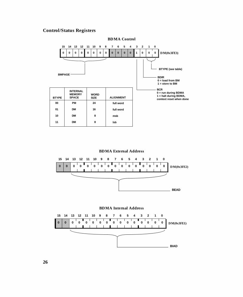
26
BDMA Control
Control/Status Registers
BDMA External Address
15 14 13 12 11 10 9 8 7 6 5 4 3 2 1 0
0000000 00 00 00 00 0 DM(0x3FE2)
BEAD
DM(0x3FE2)
BDMA Internal Address
15 14 13 12 11 10 9 8 7 6 5 4 3 2 1 0
0000000 00 00 00 00 0 DM(0x3FE1)
BIAD
DM(0x3FE1)
15 14 13 12 11 10 9 8 7 6 5 4 3 2 1 0
BMPAGE
0000000 00 00 10 00 0 DM(0x3FE3)
BDIR0 = load from BM1 = store to BM
BCR0 = run during BDMA 1 = halt during BDMA, context reset when done
BTYPE (see table)
00
01
10
11
BTYPE
INTERNALMEMORYSPACE
WORDSIZE ALIGNMENT
PM
DM
DM
DM
24
16
8
8
full word
full word
msb
lsb
DM(0x3FE3)

27
Programmable Flag & Composite Select Control
15 14 13 12 11 10 9 8 7 6 5 4 3 2 1 0
0000000 00 00 00 00 0 DM(0x3FE0)
IDMAA
IDMADDestination Memory type:0= PM, 1=DM
DM(0x3FE0)
Status Registers(Non-Memory-Mapped)
ALU Result Zero
ALU Result Negative
ALU Overflow
ALU Carry
ALU X Input Sign
ALU Quotient
MAC Overflow
Shifter Input Sign
01234567
00000000
SS MV AQ AS AC AV AN AZ
PC Stack Empty
PC Stack Overflow
Count Stack Empty
Count Stack Overflow
Status Stack Empty
Status Stack Overflow
Loop Stack Empty
Loop Stack Overflow
01234567
10101010
ASTAT SSTAT (read-only)
MSTAT
Register Bank Select 0=primary, 1=secondary
Bit-Reverse Addressing Enable (DAG1)
ALU Overflow Latch Mode Enable
AR Saturation Mode Enable
MAC Result Placement 0=fractional, 1=integer
Timer Enable
Go Mode Enable
0123456
0000000
Bit Mode Name0 SEC_REG Secondary register set1 BIT_REV Bit-reverse addressing in DAG12 AV_LATCH ALU overflow (AV) status latch3 AR_SAT AR register saturation4 M_MODE MAC result placement mode5 TIMER Timer enable6 G_MODE Go mode enable7 INTS Interrupt enable
Mode Names for Mode Control Instruction(see Miscellaneous Instructions on page 21)

28
Interrupt Registers(Non-Memory-Mapped)
ICNTL4 3 2 1 0
Interrupt Nesting
00000
1=edge0=level
1=enable0=disable
IRQ0 Sensitivity
IRQ1 Sensitivity
IRQ2 Sensitivity
IMASK
11 10 9 8 7 6 5 4 3 2 1 0
Timer
000000000000
15 14 13 12
0000
IRQL0
SPORT1 Receive or IRQ0
SPORT1 Transmit or IRQ1
IRQ2
BMDA Interrupt
IRQE
SERVICE ENABLE BITS
SPORT0 Receive
SPORT0 Transmit
IRQL1

29
Interrupt Registers(Non-Memory-Mapped)
IFC
11 10 9 8 7 6 5 4 3 2 1 0
Timer
000000000000
IRQ2
15 14 13 12
0000
Timer
SPORT1 Transmit or IRQ1
SPORT1 Receive or IRQ0
BDMA
IRQE
SPORT1 Receive or IRQ0
SPORT1 Transmit or IRQ1
IRQ2
BMDA
IRQE
INTERRUPT FORCE BITS INTERRUPT CLEAR BITS
SPORT0 Receive
SPORT0 Transmit
SPORT0 Receive
SPORT0 Transmit

30
Memory Maps
Data Memory
Data Memory Address32 Memory mapped
registers0x3FFF0x3FE0
Internal8160 words
0x3FDF
0x2000
8K Internal (DMOVLAY=0)
orExternal 8K
(DMOVLAY=1,2)
0x1FFF
0x0000
Program Memory
Program Memory Address
8K Internal (PMOVLAY = 0,
MMAP = 0 )or
External 8K(PMOVLAY = 1 or 2,
MMAP = 0)
0x3FFF
0x2000
8K Internal
0x1FFF
0x0000
MMAP = 0

31
Interrupt Vector Tables
ADSP-2181Interrupt InterruptSource Vector Address (Hex)Reset (or Power up with PUCR=1) 0000 (highest priority)Power Down (non-maskable) 002CIRQ2 0004IRQL1 0008IRQL0 000CSPORT0 Transmit 0010SPORT0 Receive 0014IRQE 0018BDMA Interrupt 001CSPORT1 Transmit or IRQ1 0020SPORT1 Receive or IRQ0 0024Timer 0028 (lowest priority)
Control/Status RegistersSymbolic names for the memory-mapped control and status registers are provided in four files includedwith the development software. The symbols are defined as constants equal to the register addresses, andcan be used for direct addressing. To use these symbols, include the appropriate file in the your sourcecode files with the assembler’s .INCLUDE directive:
Filename Include Directive To Use:DEF2181.H .INCLUDE <DEF2181.H>;
Data Memory AssemblyControl/Status Register Address Code SymbolSystem Control Register 0x3FFF Sys_Ctrl_RegData Memory Wait State Control Register 0x3FFE Dm_Wait_RegTimer Period 0x3FFD Tperiod_RegTimer Count 0x3FFC Tcount_RegTimer Scaling Factor 0x3FFB Tscale_RegSPORT0 Multichannel Receive 0x3FFA Sport0_Rx_Words1 Word Enable Register (32-bit) 0x3FF9 Sport0_Rx_Words0SPORT0 Multichannel Transmit 0x3FF8 Sport0_Tx_Words1 Word Enable Register (32-bit) 0x3FF7 Sport0_Tx_Words0SPORT0 Control Register 0x3FF6 Sport0_Ctrl_RegSPORT0 Serial Clock Divide Modulus 0x3FF5 Sport0_SclkdivSPORT0 Rcv Frame Sync Divide Modulus 0x3FF4 Sport0_RfsdivSPORT0 Autobuffer Control Register 0x3FF3 Sport0_Autobuf_CtrlSPORT1 Control Register 0x3FF2 Sport1_Ctrl_RegSPORT1 Serial Clock Divide Modulus 0x3FF1 Sport1_SclkdivSPORT1 Rcv Frame Sync Divide Modulus 0x3FF0 Sport1_RfsdivSPORT1 Autobuffer Control Register 0x3FEF Sport1_Autobuf_CtrlProgrammable Flag & Composite Select 0x3FE6 Prog_Flag_Comp_Sel_CtrlProgrammable Flag Data 0x3FE5 Prog_Flag_DataBDMA Word Count 0x3FE4 BDMA_Word_CountBDMA Control 0x3FE3 BDMA_ControlBDMA External Address 0x3FE2 BDMA_External_AdressBDMA Internal Address 0x3FE1 BDMA_Internal_AddressIDMA Control 0x3FE0 IDMA_Control

32
AD
SP
-218
1 R
egis
ters
DA
TA
SR
AM
16K
X 1
6
TIM
ER
TP
ER
IOD
TC
OU
NT
TS
CA
LE
0x3F
FD
0x3F
FC
0x3F
FB
IDM
A
Po
rt
FL
AG
S
PO
WE
RD
OW
NC
ON
TR
OL
LO
GIC
IDM
AA
AL
U
MA
CS
HIF
TE
R
DM
D B
US
DA
G 2
DA
G 1
PM
D B
US
DM
A B
US
PM
A B
US
14 14 24 16
PR
OG
RA
M S
EQ
UE
NC
ER
M0
M1
M2
M3
I3I0 I1 I2
L0 L1 L2 L3
CN
TR
M5
M6
M7
I7I4 I5 I6
OW
RC
NT
R
L5 L6 L7
AX
0A
X1
AY
1A
Y0
MX
0M
X1
MY
1M
Y0
SI
SE
SBR
X1
TX1
PX
CO
UN
T
ST
AC
K4
X 1
4
AS
TA
T
ST
AT
US
S
TA
CK
12 X
25
MS
TA
TIM
AS
K
PC
S
TA
CK
16 X
14
LO
OP
S
TA
CK
4 X
18
IFC
ICN
TL
SS
TAT
AF
AR
MR
0M
R1
MF
MR
2S
R0
SR
1
M4
L4
DM
WA
IT C
ON
TR
OL
SY
ST
EM
CO
NT
RO
L
SP
OR
T 0
RX
0TX
0
CO
NT
RO
L R
EG
IST
ER
S
0x3F
FA
-0x3
FF
3
SP
OR
T 1
CO
NT
RO
L R
EG
IST
ER
S
0x3F
F2-
0x3F
EF
0x3F
FF
0x3F
FE
PR
OG
RA
MS
RA
M16
K X
24
PM
OV
LA
Y
DM
OV
LA
Y
BY
TE
DM
A
PO
RT
BT
YP
E
BIA
D
BE
AD
BM
PA
GE
BD
IR
BW
CO
UN
T
PR
OG
RA
MM
AB
LE
I/O
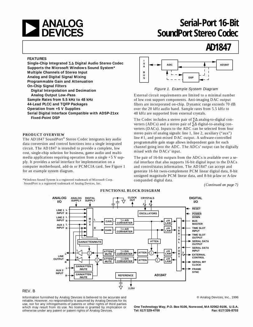
REV. B
Information furnished by Analog Devices is believed to be accurate andreliable. However, no responsibility is assumed by Analog Devices for itsuse, nor for any infringements of patents or other rights of third partieswhich may result from its use. No license is granted by implication orotherwise under any patent or patent rights of Analog Devices.
a Serial-Port 16-BitSoundPort Stereo Codec
AD1847
® Analog Devices, Inc., 1996
One Technology Way, P.O. Box 9106, Norwood, MA 02062-9106, U.S.A.
Tel: 617/329-4700 Fax: 617/326-8703
FEATURES
Single-Chip Integrated SD Digital Audio Stereo Codec
Supports the Microsoft Windows Sound System*
Multiple Channels of Stereo Input
Analog and Digital Signal Mixing
Programmable Gain and Attenuation
On-Chip Signal Filters
Digital Interpolation and Decimation
Analog Output Low-Pass
Sample Rates from 5.5 kHz to 48 kHz
44-Lead PLCC and TQFP Packages
Operation from +5 V Supplies
Serial Digital Interface Compatible with ADSP-21xx
Fixed-Point DSP
ISA
BUS
ASIC AD1847
DSP
Figure 1. Example System Diagram
External circuit requirements are limited to a minimal numberof low cost support components. Anti-imaging DAC outputfilters are incorporated on-chip. Dynamic range exceeds 70 dBover the 20 kHz audio band. Sample rates from 5.5 kHz to48 kHz are supported from external crystals.
The Codec includes a stereo pair of ∑∆ analog-to-digital con-verters (ADCs) and a stereo pair of ∑∆ digital-to-analog con-verters (DACs). Inputs to the ADC can be selected from fourstereo pairs of analog signals: line 1, line 2, auxiliary (“aux”)line #1, and post-mixed DAC output. A software-controlledprogrammable gain stage allows independent gain for eachchannel going into the ADC. The ADCs’ output can be digitallymixed with the DACs’ input.
The pair of 16-bit outputs from the ADCs is available over a se-rial interface that also supports 16-bit digital input to the DACsand control/status information. The AD1847 can accept andgenerate 16-bit twos-complement PCM linear digital data, 8-bitunsigned magnitude PCM linear data, and 8-bit µ-law or A-lawcompanded digital data.
(Continued on page 7)
FUNCTIONAL BLOCK DIAGRAM
ANALOGI/O
L
R
DIGITALI/O
CRYSTALS
2 2
2
SERIAL
PORT
OSCILLATORS
2.25V
REFERENCE
L
R
L
R
CLOCK OUT
ATTEN
DIGITAL SUPPLY
ANALOGSUPPLY
MUX
LR
L
RL
R
L
R
BUS MASTER
TIME SLOTINPUT
TIME SLOTOUTPUTSERIAL DATAOUTPUT
SERIAL DATA INPUT
EXTERNALCONTROL
SERIAL BITCLOCK
FRAMESYNC
RESETLINE 1INPUT
LINE 2INPUT
AUX 1INPUT
LINEOUTPUT
AUX 2INPUT
AD1847
∑
ATTEN/MUTE ATTEN
POWERDOWN
µ/A LAW
µ/A LAWATTEN
∑
∑
∑
∑∆ D/ACONVERTER
∑∆ D/ACONVERTER
µ/A LAW
µ/A LAW
GAIN
GAIN ∑∆ A/DCONVERTER
∑∆ A/DCONVERTER
GAIN/ATTEN/MUTE
GAIN/ATTEN/MUTE
GAIN/ATTEN/MUTE
ATTEN/MUTE
PRODUCT OVERVIEWThe AD1847 SoundPort® Stereo Codec integrates key audiodata conversion and control functions into a single integratedcircuit. The AD1847 is intended to provide a complete, lowcost, single-chip solution for business, game audio and multi-media applications requiring operation from a single +5 V sup-ply. It provides a serial interface for implementation on acomputer motherboard, add-in or PCMCIA card. See Figure 1for an example system diagram.
*Windows Sound System is a registered trademark of Microsoft Corp.SoundPort is a registered trademark of Analog Devices, Inc.

STANDARD TEST CONDITIONS UNLESS OTHERWISE NOTED
Temperature 25 °C DAC Output ConditionsDigital Supply (VDD) 5.0 V 0 dB AttenuationAnalog Supply (VCC) 5.0 V Full-Scale Digital InputsWord Rate (FS ) 48 kHz 16-Bit Linear ModeInput Signal 1007 Hz No Output LoadAnalog Output Passband 20 Hz to 20 kHz Mute OffFFT Size 4096 ADC Input ConditionsVIH 2.4 V 0 dB GainVIL 0.8 V –3.0 dB Relative to Full ScaleVOH 2.4 V Line InputVOL 0.4 V 16-Bit Linear Mode
ANALOG INPUT
Min Typ Max Units
Full-Scale Input Voltage (RMS Values Assume Sine Wave Input)Line1, Line2, AUX1, AUX2 1 V rms
2.54 2.8 3.10 V p-pInput Impedance
Line1, Line2, AUX1, AUX2† 10 kΩInput Capacitance† 15 pF
PROGRAMMABLE GAIN AMPLIFIER—ADC
Min Typ Max Units
Step Size (All Steps Tested, –30 dB Input) 1.10 1.5 1.90 dBPGA Gain Range Span† 21.0 24.0 dB
AUXILIARY INPUT ANALOG AMPLIFIERS/ATTENUATORS
Min Typ Max Units
Step Size (+12 dB to –28.5 dB, Referenced to DAC Full Scale) 1.3 1.5 1.7 dB(–30 dB to –34.5 dB, Referenced to DAC Full Scale) 1.1 1.5 1.9 dB
Input Gain/Attenuation Range Span† 45.5 47.5 dBAUX Input Impedance† 10 kΩ
DIGITAL DECIMATION AND INTERPOLATION FILTERS†
Min Max Units
Passband 0 0.4 3 FS HzPassband Ripple –0.1 +0.1 dBTransition Band 0.4 3 FS 0.6 3 FS HzStopband 0.6 3 FS ∞ HzStopband Rejection 74 dBGroup Delay 30/FS
Group Delay Variation Over Passband 0 µs
REV. B
AD1847–SPECIFICATIONS
–2–

ANALOG-TO-DIGITAL CONVERTERS
Min Typ Max Units
Resolution 16 BitsDynamic Range (–60 dB Input, THD+N Referenced to Full Scale, A-Weighted) 70 dBTHD+N (Referenced to Full Scale) 0.040 %
–68 dBSignal-to-Intermodulation Distortion† 83 dBADC Crosstalk†
Line Inputs (Input L, Ground R, Read R; Input R, Ground L, Read L) –80 dBLine1 to Line2 (Input Line1, Ground and Select Line2, Read Both Channels) –80 dBLine to AUX1 –80 dBLine to AUX2 –80 dBLine to DAC –80 dB
Gain Error (Full-Scale Span Relative to VREFI) ±10 %Interchannel Gain Mismatch (Difference of Gain Errors) ±0.2 dBDC Offset ±55 LSB
DIGITAL-TO-ANALOG CONVERTERS
Min Typ Max Units
Resolution 16 BitsDynamic Range (–60 dB Input, THD+N Referenced to Full Scale, A-Weighted) 76 dBTHD+N (Referenced to Full Scale) 0.025 %
–72 dBSignal-to-Intermodulation Distortion† 86 dBGain Error (Full-Scale Span Relative to VREFI) ±10 %Interchannel Gain Mismatch (Difference of Gain Errors) ±0.2 dBDAC Crosstalk† (Input L, Zero R, Measure R_OUT; Input R, Zero L, Measure L_OUT) –80 dBTotal Out-of-Band Energy† (Measured from 0.6 3 FS to 100 kHz) –50 dBAudible Out-of-Band Energy (Measured from 0.6 3 FS to 22 kHz, Tested at FS = 5.5 kHz) –55 dB
DAC ATTENUATOR
Min Typ Max Units
Step Size (0 dB to –22.5 dB) (Tested at Steps 0 dB, –19.5) 1.3 1.5 1.7 dBStep Size (–24 dB to –94 dB) 1.0 1.5 2.0 dBOutput Attenuation Range Span† –93 95 dB
DIGITAL MIX ATTENUATOR
Min Typ Max Units
Step Size (0 dB to –22.5 dB) (Tested at Steps 0 dB, –19.5) 1.3 1.5 1.7 dBStep Size (–24 dB to –94 dB) 1.0 1.5 2.0 dBOutput Attenuation Range Span† –93.5 95.5 dB
ANALOG OUTPUT
Min Typ Max Units
Full-Scale Line Output Voltage 0.707 V rmsVREFI = 2.35* 1.80 2 2.20 V p-p
Line Output Impedance† 600 ΩExternal Load Impedance 10 kΩOutput Capacitance† 15 pFExternal Load Capacitance 100 pFVREF (Clock Running) 2.00 2.50 VVREF Current Drive 100 µAVREFI 2.35 VMute Attenuation of 0 dB –80 dB
Fundamental† (LOUT)Mute Click† 8 mV
(|Muted Output Minus UnmutedMidscale DAC Output|)
*Full-scale line output voltage scales with VREF (e.g., VOUT (typ) – 2.0 V 3 (VREF/2.35)).†Guaranteed, Not Tested.
REV. B –3–
AD1847

AD1847
REV. B–4–
SYSTEM SPECIFICATIONS
Min Typ Max Units
System Frequency Response† ±0.3 dB(Line In to Line Out, 20 Hz to 20 kHz)
Differential Nonlinearity† ±1/2 BitPhase Linearity Deviation† 1 Degrees
STATIC DIGITAL SPECIFICATIONS
Min Max Units
High Level Input Voltage (VIH)Digital Inputs 2.0 VXTAL1/2I 2.4 V
Low Level Input Voltage (VIL) 0.8 VHigh Level Output Voltage (VOH) IOH = 1 mA 2.4 VDD VLow Level Output Voltage (VOL) IOL = 4 mA 0.4 VInput Leakage Current (GO/NOGO Tested) –10 +10 µAOutput Leakage Current (GO/NOGO Tested) –10 +10 µA
TIMING PARAMETERS (Guaranteed Over Operating Temperature Range)
Min Typ Max Units
Serial Frame Sync Period (t1) 1/0.5 FS µsClock to Frame Sync [SDFS] Propagation Delay (tPD1) 20 nsData Input Setup Time (tS) 15 nsData Input Hold Time (tH) 15 nsClock to Output Data Valid (tDV) 25 nsClock to Output Three-State [High-Z] (tHZ) 20 nsClock to Time Slot Output [TSO] Propagation Delay (tPD2) 20 nsRESET and PWRDOWN Lo Pulse Width (tRPWL) 100 ns
POWER SUPPLY
Min Max Units
Power Supply Range – Digital & Analog 4.75 5.25 VPower Supply Current – Operating (10 kΩ Line Out Load) 140 mAAnalog Supply Current – Operating (10 kΩ Line Out Load) 70 mADigital Supply Current – Operating (10 kΩ Line Out Load) 70 mAAnalog Power Supply Current – Power Down 400 µADigital Power Supply Current – Power Down 400 µAPower Dissipation – Operating (Current 3 Nominal Supply) 750 mWPower Dissipation – Power Down (Current 3 Nominal Supply) 4 mWPower Supply Rejection (@ 1 kHz)†
(At Both Analog and Digital Supply Pins, ADCs) 45 dB(At Both Analog and Digital Supply Pins, DACs) 55 dB
CLOCK SPECIFICATIONS†
Min Max Units
Input Clock Frequency 27 MHzRecommended Clock Duty Cycle ±10 %Initialization/Sample Rate Change Time
16.9344 MHz Crystal Selected at Power-Up 171 ms24.576 MHz Crystal Selected at Power-Up 171 ms16.9344 MHz Crystal Selected Subsequently 6 ms24.576 MHz Crystal Selected Subsequently 6 ms
†Guaranteed, not tested. Specifications subject to change without notice.

AD1847
REV. B –5–
ABSOLUTE MAXIMUM RATINGS*
Min Max Units
Power SuppliesDigital (VDD) –0.3 6.0 VAnalog (VCC) –0.3 6.0 V
Input Current(Except Supply Pins) ±10.0 mA
Analog Input Voltage (Signal Pins) –0.3 (VA+) + 0.3 VDigital Input Voltage (Signal Pins) –0.3 (VD+) + 0.3 VAmbient Temperature (Operating) 0 +70 °CStorage Temperature –65 +150 °C*Stresses greater than those listed under “Absolute Maximum Ratings” may cause
permanent damage to the device. This is a stress rating only and functionaloperation of the device at these or any other conditions above those indicated inthe operational section of this specification is not implied. Exposure to absolutemaximum rating conditions for extended periods may affect device reliability.
ORDERING GUIDE
Temperature Package PackageModel Range Description Option*
AD1847JP 0°C to +70°C 44-Lead PLCC P-44AAD1847JST 0°C to +70°C 44-Lead TQFP ST-44
*P = PLCC; ST = TQFP.
WARNING!
ESD SENSITIVE DEVICE
CAUTIONESD (electrostatic discharge) sensitive device. Electrostatic charges as high as 4000 V readilyaccumulate on the human body and test equipment and can discharge without detection.Although the AD1847 features proprietary ESD protection circuitry, permanent damage mayoccur on devices subjected to high energy electrostatic discharges. Therefore, proper ESDprecautions are recommended to avoid performance degradation or loss of functionality.
44-Lead PLCC 44-Lead TQFP
R_L
INE
2
RFI
LT
L_L
INE
2
L_L
INE
1
GN
DA
GN
DA
LF
ILT
L_A
UX
1
R_A
UX
1
R_O
UT
VC
C
SD
FS
SD
O
VD
D
SC
LK
CL
KO
UT
SD
I
GN
DD
XT
AL
2I
XT
AL
1O
XT
AL
1I
XT
AL
2O
VDD
GNDD
GNDD
VDD
BM
XCTL1
XCTL0
R_AUX2
L_OUT
N/C
L_AUX2
44126 45
21 24232218 2019
39
38
35
34
33
37
36
3
7
8
11
12
13
9
10
404142
25 282726
43
31
30
29
32
15
16
17
14
Top View(Not to Scale)
AD1847JP
TSO
TSI
RESET
PWRDOWN
VCC
VDD
GNDD
VREFI
VREF
R_LINE1
GNDA
N/C = NO CONNECT
44 S
DF
S43
SD
O42
SD
I41
GN
DD
40 V
DD
39 S
CL
K38
CL
KO
UT
37 X
TA
L2O
36 X
TA
L2I
35 X
TA
L1O
34 X
TA
L1I
33323130292827262524
23
PIN 1 IDENTIFIER
R_LINE1
VREF
VREFI
GNDA
VCC
PWRDOWNRESETGNDD
VDD
TSITSO 1
234
56789
1110
VDDGNDDXCTL1XCTL0GNDDVDD
BML_AUX2R_AUX2L_OUT
N/C
R_L
INE
2 12
RF
ILT
13
GN
DA
14
LF
ILT
15
L_L
INE
2 16
L_L
INE
1 17
GN
DA
18
L_A
UX
1 20
R_A
UX
1 21
R_O
UT
22
VC
C 1
9
Top View(Not to Scale)
AD1847JST
N/C = NO CONNECT
PINOUTS

AD1847
REV. B–6–
PIN DESCRIPTIONSParallel Interface
Pin Name PLCC TQFP I/O Description
SCLK 1 39 I/O Serial Clock. SCLK is a bidirectional signal that supplies the clock as an output to theserial bus when the Bus Master (BM) pin is driven HI and accepts the clock as an inputwhen the BM pin is driven LO. The serial clock output is fixed at 12.288 MHz whenXTAL1 is selected, and 11.2896 MHz when XTAL2 is selected. SCLK runs continu-ously. An AD1847 should always be configured as the serial bus master unless it is a slavein a daisy-chained multiple codec system.
SDFS 6 44 I/O Serial Data Frame Sync. SDFS is a bidirectional signal that supplies the frame synchroni-zation signal as an output to the serial bus when the Bus Master (BM) pin is driven HIand accepts the frame synchronization signal as an input when the BM pin is driven LO.The SDFS frequency powers up at one half of the AD1847 sample rate (i.e., FRS bit = 0)with two samples per frame and can be programmed to match the sample rate (i.e., FRSbit = 1) with one sample per frame. An AD1847 should always be configured as the serialbus master unless it is a slave in a daisy-chained multiple codec system.
SDI 4 42 I Serial Data Input. SDI is used by peripheral devices such as the host CPU or a DSP tosupply control and playback data information to the AD1847. All control and playbacktransfers are 16 bits long, MSB first.
SDO 5 43 O Serial Data Output. SDO is used to supply status/index readback and capture data infor-mation to peripheral devices such as the host CPU or a DSP. All status/index readbackand capture data transfers are 16 bits long, MSB first. Three-state output driver.
RESET 11 5 I Reset. The RESET signal is active LO. The assertion of this signal will initialize theon-chip registers to their default values. See the “Control Register Definitions” section fora description of the contents of the control registers after RESET is deasserted.
PWRDOWN 12 6 I Powerdown. The PWRDOWN signal is active LO. The assertion of this signal will resetthe on-chip control registers (identically to the RESET signal) and will also place theAD1847 in a low power consumption mode. VREF and all analog circuitry are disabled.
BM 33 27 I Bus Master. The assertion (HI) of this signal indicates that the AD1847 is the serial busmaster. The AD1847 will then supply the serial clock (SCLK) and the frame sync (SDFS)signals for the serial bus. One and only one AD1847 should always be configured as theserial bus master. If BM is connected to logic LO, the AD1847 is configured as a busslave, and will accept the SCLK and SDFS signals as inputs. An AD1847 should only beconfigured as a serial bus slave when an AD1847 serial bus master already exists, indaisy-chained multiple codec systems.
TSO 7 1 O Time Slot Output. This signal is asserted HI by the AD1847 coincidentally with the LSBof the last time slot used by the AD1847. Used in daisy-chained multiple codec systems.
TSI 8 2 I Time Slot Input. The assertion of this signal indicates that the AD1847 should immedi-ately use the next three time slots (TSSEL = 1) or the next six time slots (TSSEL = 0)and then activate the TSO pin to enable the next device down the TDM chain. TSIshould be driven LO when the AD1847 is the bus master or in single codec systems. Usedin daisy-chained multiple codec systems.
CLKOUT 44 38 O Clock Output. This signal is the buffered version of the crystal clock output and the fre-quency is dependent on which crystal is selected. This pin can be three-stated by drivingthe BM pin LO or by programming the CLKTS bit in the Pin Control Register. See the“Control Registers” section for more details. The CLKOUT frequency is 12.288 MHzwhen XTAL1 is selected and 16.9344 MHz when XTAL2 is selected.
Analog Signals
Pin Name PLCC TQFP I/O Description
L_LINE1 23 17 I Left Line Input #1. Line level input for the #1 left channel.R_LINE1 17 11 I Right Line Input #1. Line level input for the #1 right channel.L_LINE2 22 16 I Left Line Input #2. Line level input for the #2 left channel.R_LINE2 18 12 I Right Line Input #2. Line level input for the #2 right channel.L_AUX1 26 20 I Left Auxiliary Input #1. Line level input for the AUX1 left channel.R_AUX1 27 21 I Right Auxiliary Input #1. Line level input for the AUX1 right channel.L_AUX2 32 26 I Left Auxiliary Input #2. Line level input for the AUX2 left channel.R_AUX2 31 25 I Right Auxiliary Input #2. Line level input for the AUX2 right channel.L_OUT 30 24 O Left Line Output. Line level output for the left channel.R_OUT 28 22 O Right Line Output. Line level output for the right channel.

AD1847
REV. B –7–
Miscellaneous
Pin Name PLCC TQFP I/O Description
XTAL1I 40 34 I 24.576 MHz Crystal #1 Input.
XTAL1O 41 35 O 24.576 MHz Crystal #1 Output.
XTAL2I 42 36 I 16.9344 MHz Crystal #2 Input.
XTAL2O 43 37 O 16.9344 MHz Crystal #2 Output.
XCTL1:O 37 & 36 31 & 30 O External Control. These TTL signals reflect the current status of register bits inside theAD1847. They can be used for signaling or to control external logic.
VREF 16 10 O Voltage Reference. Nominal 2.25 volt reference available externally as a voltage datumfor dc-coupling and level-shifting. VREF should not have any signal dependent load.
VREFI 15 9 I Voltage Reference Internal. Voltage reference filter point for external bypassing only.
L_FILT 21 15 I Left Channel Filter Capacitor. This pin requires a 1.0 µF capacitor to analog groundfor proper operation.
R_FILT 19 13 I Right Channel Filter Capacitor. This pin requires a 1.0 µF capacitor to analog groundfor proper operation.
NC 29 23 No Connect. Do not connect.
Power Supplies
Pin Name PLCC TQFP I/O Description
VCC 13 & 25 7 & 19 I Analog Supply Voltage (+5 V).
GNDA 14, 20, 24 8, 14, 18 I Analog Ground.
VDD 2, 9, 34, 39 40, 3, 28, 33 I Digital Supply Voltage (+5 V).
GNDD 3, 10, 35, 38 41, 4, 29, 32 I Digital Ground.
(Continued from page 1)
The ∑∆ DACs are preceded by a digital interpolation filter. Anattenuator provides independent user volume control over eachDAC channel. Nyquist images are removed from the DACs’analog stereo output by on-chip switched-capacitor andcontinuous-time filters. Two stereo pairs of auxiliary line-levelinputs can also be mixed in the analog domain with the DACoutput.
The AD1847 serial data interface uses a Time Division Multi-plex (TDM) scheme that is compatible with DSP serial portsconfigured in Multi-Channel Mode with 32 16-bit time slots(i.e., SPORT0 on the ADSP-2101, ADSP-2115, etc.).
AUDIO FUNCTIONAL DESCRIPTIONThis section overviews the functionality of the AD1847 and isintended as a general introduction to the capabilities of the de-vice. As much as possible, detailed reference information hasbeen placed in “Control Registers” and other sections. The useris not expected to refer repeatedly to this section.
Analog InputsThe AD1847 SoundPort Stereo Codec accepts stereo line-levelinputs. All inputs should be capacitively coupled (ac-coupled) tothe AD1847. LINE1, LINE2, and AUX1, and post-mixed DACoutput analog stereo signals are multiplexed to the internal pro-grammable gain amplifier (PGA) stage.
The PGA following the input multiplexer allows independentselectable gains for each channel from 0 to 22.5 dB in +1.5 dBsteps. The Codec can operate either in a global stereo mode orin a global mono mode with left-channel inputs appearing atboth channel outputs.
Analog MixingAUX1 and AUX2 analog stereo signals can be mixed in the ana-log domain with the DAC output. Each channel of each auxil-iary analog input can be independently gained/attenuated from+12 dB to –34.5 dB in –1.5 dB steps or completely muted. Thepost-mixed DAC output is available on L_OUT and R_OUTexternally and as an input to the ADCs.
Even if the AD1847 is not playing back data from its DACs, theanalog mix function can still be active.
Analog-to-Digital DatapathThe ∑∆ ADCs incorporate a proprietary fourth-order modula-tor. A single pole of passive filtering is all that is required forantialiasing the analog input because of the ADC’s high 64times oversampling ratio. The ADCs include digital decimationfilters that low-pass filter the input to 0.4 3 FS. (“FS’’ is theword rate or “sampling frequency.”) ADC input overrange con-ditions will cause status bits to be set that can be read.
Digital-to-Analog DatapathThe ∑∆ DACs contain a programmable attenuator and a low-pass digital interpolation filter. The anti-imaging interpolationfilter oversamples and digitally filters the higher frequency im-ages. The attenuator allows independent control of each DACchannel from 0 dB to –94.5 dB in 1.5 dB steps plus full mute.The DACs’ ∑∆ noise shapers also oversample and convert thesignal to a single-bit stream. The DAC outputs are then filteredin the analog domain by a combination of switched-capacitorand continuous-time filters. These filters remove the very highfrequency components of the DAC bitstream output. No exter-nal components are required.

AD1847
REV. B–8–
Changes in DAC output attenuation take effect only on zerocrossings of the digital signal, thereby eliminating “zipper” noiseon playback. Each channel has its own independent zero-crossingdetector and attenuator change control circuitry. A timer guar-antees that requested volume changes will occur even in the ab-sence of an input signal that changes sign. The time-out periodis 8 milliseconds at a 48 kHz sampling rate and 48 millisecondsat an 8 kHz sampling rate. (Time-out [ms] ≈ 384/FS [kHz]).
Digital MixingStereo digital output from the ADCs can be mixed digitally withthe input to the DACs. Digital output from the ADCs going outof the serial data port is unaffected by the digital mix. Along thedigital mix datapath, the 16-bit linear output from the ADCs isattenuated by an amount specified with control bits. Both chan-nels of the monitor data are attenuated by the same amount.(Note that internally the AD1847 always works with 16-bitPCM linear data, digital mixing included; format conversionstake place at the input and output.)
Sixty-four steps of –1.5 dB attenuation are supported to–94.5 dB. The digital mix datapath can also be completelymuted, preventing any mixing of the digital input with the digi-tal output. Note that the level of the mixed signal is also a func-tion of the input PGA settings, since they affect the ADCs’output.
The attenuated digital mix data is digitally summed with theDAC input data prior to the DACs’ datapath attenuators. Thedigital sum of digital mix data and DAC input data is clipped atplus or minus full scale and does not wrap around. Becauseboth stereo signals are mixed before the output attenuators, mixdata is attenuated a second time by the DACs’ datapathattenuators.
Analog OutputsA stereo line-level output is available at external pins. Otheroutput types such as headphone and speaker must be imple-mented in external circuitry. The stereo line-level outputsshould be capacitively coupled (ac-coupled) to the external cir-cuitry. Each channel of this output can be independentlymuted. When muted, the outputs will settle to a dc value nearVREF, the midscale reference voltage.
Digital Data TypesThe AD1847 supports four global data types: 16-bit twos-complement linear PCM, 8-bit unsigned linear PCM,companded µ-law, and 8-bit companded A-law, as specified bycontrol register bits. Eight-bit data is always left-justified in 16-bit fields; in other words, the MSBs of all data types are alwaysaligned; in yet other words, full-scale representations in all fourformats correspond to equivalent full-scale signals. The eightleast significant bit positions of 8-bit data in 16-bit fields are ig-nored on digital input and zoned on digital output (i.e., truncated).
The 16-bit PCM data format is capable of representing 96 dB ofdynamic range. Eight-bit PCM can represent 48 dB of dynamicrange. Companded µ-law and A-law data formats use nonlinearcoding with less precision for large-amplitude signals. The lossof precision is compensated for by an increase in dynamic rangeto 64 dB and 72 dB, respectively.
On input, 8-bit companded data is expanded to an internal lin-ear representation, according to whether µ-law or A-law was
specified in the Codec’s internal registers. Note that when µ-lawcompressed data is expanded to a linear format, it requires 14bits. A-law data expanded requires 13 bits.
EXPANSION
DAC INPUT
MSB LSB
15 0
MSB
15 0
MSB
15 0
COMPRESSEDINPUT DATA
LSB
3/2 2/1
LSB
3/2 2/1
0 0 0 / 0 0
8 7
Figure 2. A-Law or µ-Law Expansion
When 8-bit companding is specified, the ADCs’ linear output iscompressed to the format specified.
TRUNCATION
COMPRESSION
MSB LSB
15 0
MSB LSB
15 0
MSB LSB
15 0
3/2 2/1
ADC OUTPUT
0 0 0 0 0 0 0 0
8 7
Figure 3. A-Law or µ-Law Compression
Note that all format conversions take place at input or output.Internally, the AD1847 always uses 16-bit linear PCM represen-tations to maintain maximum precision.
Power Supplies and Voltage ReferenceThe AD1847 operates from +5 V power supplies. Independentanalog and digital supplies are recommended for optimal perfor-mance though excellent results can be obtained in single-supplysystems. A voltage reference is included on the Codec and its2.25 V buffered output is available on an external pin (VREF).The reference output can be used for biasing op amps used indc coupling. The internal reference must be externally bypassedto analog ground at the VREFI pin, and must not be used to biasexternal circuitry.
Clocks and Sample RatesThe AD1847 operates from two external crystals, XTAL1 andXTAL2. The two crystal inputs are provided to generate a widerange of sample rates. The oscillators for these crystals are onthe AD1847, as is a multiplexer for selecting between them.They can be overdriven with external clocks by the user, if sodesired. At a minimum, XTAL1 must be provided since it is se-lected as the reset default. If XTAL2 is not used, the XTAL2input pin should be connected to ground. The recommendedcrystal frequencies are 16.9344 MHz and 24.576 MHz. Fromthem, the following sample rates can be selected: 5.5125, 6.615,8, 9.6, 11.025, 16, 18.9, 22.05, 27.42857, 32, 33.075, 37.8,44.1, 48 kHz.

AD1847
REV. B –9–
CONTROL REGISTERSControl Register MappingThe AD1847 has six 16-bit and thirteen 8-bit on-chip user-accessible control registers. Control information is sent to theAD1847 in the 16-bit Control Word. Status information is sentfrom the AD1847 in the 16-bit Status Word. Playback Data andCapture Data each have two 16-bit registers for the right andleft channels. Additional 8-bit Index Registers are accessed viaindirect addressing in the AD1847 Control Word. [Index Regis-ters are reached with indirect addressing.] The contents of anindirect addressed Index Register may be readback by the hostCPU or DSP (during the Status Word/Index Readback timeslot) by setting the Read Request (RREQ) bit in the ControlWord. Note that each 16-bit register is assigned its own timeslot, so that the AD1847 always consumes six 16-bit time slots.Figure 4 shows the mapping of the Control Word, Status Word/Index Readback and Data registers to time slots when TSSEL = 0.TSSEL = 0 is used when the SDI and SDO pins are tied to-gether (i.e., “1-wire” system). This configuration is efficient interms of component interconnect (one bidirectional wire for se-rial data input and output), but inefficient in terms of time slotusage (six slots consumed on single bidirectional Time DivisionMultiplexed [TDM] serial bus). When TSSEL = 0, serial datainput to the AD1847 occurs sequentially with serial data outputfrom the AD1847 (i.e., Control Word, Left Playback and RightPlayback data is received on the SDI pin, then the Status Word/lndex Readback, Left Capture and Right Capture data is trans-mitted on the SDO pin).
Slot Register Name (16-Bit)
0 Control Word Input1 Left Playback Data Input2 Right Playback Data Input3 Status Word/Index Readback Output4 Left Capture Data Output5 Right Capture Data Output
Figure 4. Control Register Mapping with TSSEL = 0
Figure 5 shows the mapping of the Control Word, Status Word/Index Readback and Data registers to time slots when TSSEL =1. Note that the six 16-bit registers “share” three time slots.TSSEL = 1 is used when the SDI and SDO pins are indepen-dent inputs and output (i.e., “2-wire” system). This configura-tion is inefficient in terms of component interconnect (twounidirectional wires for serial data input and output), but effi-cient in terms of time slot usage (three slots consumed on eachof two unidirectional TDM serial buses). When TSSEL = 1, se-rial data input to the AD1847 occurs concurrently with serialdata output from the AD1847 (i.e., Control Word reception onthe SDI pin occurs simultaneously with Status Word/lndexReadback transmission on the SDO pin).
Slot Register Name (16-Bit)
0 Control Word Input1 Left Playback Data Input2 Right Playback Data Input0 Status Word/Index Readback Output1 Left Capture Data Output2 Right Capture Data Output
Figure 5. Control Register Mapping with TSSEL = 1
An Index Register readback request to an invalid index address(11, 14 and 15) will return the contents of the Status Word. At-tempts to write to an invalid index address (11, 14 and 15) willhave no effect on the AD1847. As mentioned above, the RREQbit of the Control Word is used to request Status Word outputor Index Register readback output during either time slot 3(TSSEL = 0) or time slot 0 (TSSEL = 1). RREQ is set for In-dex Register readback output, and reset for Status Word output.When Index Register readback is requested, the Index Readbackbit format is the same as the Control Word bit format. All statusbits are updated by the AD1847 before a new Control Word isreceived (i.e., at frame boundaries). Thus, if TSSEL = 0 andthe Control Word written at slot 0 causes some status bits tochange, the change will show up in the Status Word transmittedat slot 3 of the same sample.

AD1847
REV. B–10–
Control Word (16-Bit)
Data 15 Data 14 Data 13 Data 12 Data 11 Data 10 Data 9 Data 8CLOR MCE RREQ res IA3 IA2 IA1 IA0
Data 7 Data 6 Data 5 Data 4 Data 3 Data 2 Data 1 Data 0DATA7 DATA6 DATA5 DATA4 DATA3 DATA2 DATA1 DATA0
DATA7:0 Index Register Data. These bits are the data for the desired AD1847 Index Register referenced by the Index Address.Written by the host CPU or DSP to the AD1847.
IA3:0 Index Register Address. These bits define the indirect address of the desired AD1847 Index Register. Written by the hostCPU or DSP to the AD1847.
RREQ Read Request. Setting this bit indicates that the current transfer is a request by the host CPU or DSP for readback of thecontents of the indirect addressed Index Register. When this bit is set (RREQ = HI), the AD1847 will not transmit itsStatus Word in the following Status Word Index readback slot, but will instead transmit the data in the Index Registerspecified by the Index Address. Although the Index Readback is transmitted in the following Status Word/IndexReadback time slot, the format of the Control Word is used (i.e., CLOR, MCE, RREQ and the Index Register Addressin the most significant byte, and the readback Index Register Data in the least significant byte). When this bit is reset(RREQ = LO), the AD1847 will transmit its Status Word in the following Status Word Index Readback time slot.
A read request is serviced in the next available Index Readback time slot. If TSSEL = 0, the Index Register readbackdata is transmitted in slot 3 of the same sample. If TSSEL = 1, Index Register readback data is transmitted in slot 0 ofthe next sample. If TSSEL changes from 0 to 1, Index Register readback will occur twice, in slot 3 of the current sample,and slot 0 of the next. If TSSEL changes from 1 to 0, the last read request is lost.
res Reserved for future expansion. Write zeros (LO) to all reserved bits.
MCE Mode Change Enable. This bit must be set (MCE = HI) whenever protected control register bits of the AD1847 arechanged. The Data Format register, the Miscellaneous Information register, and the ACAL bit of the Interface Configu-ration register can NOT be changed unless this bit is set. The DAC outputs will be muted when MCE is set. The usermust mute the AUX1 and AUX2 channels when this bit is set (no audio activity should occur). Written by the host CPUor DSP to the AD1847. This bit is HI after reset.
CLOR Clear Overrange. When this bit is set (CLOR = HI), the overrange bits in the Status Word are updated every sample.When this bit is reset (CLOR = LO), the overrange bits in the Status Word will record the largest overrange value. Thelargest overrange value is sticky until the CLOR bit is set. Written by the host CPU or DSP to the AD1847. Since therecan be up to 2 samples in the data pipeline, a change to CLOR may take up to 2 samples periods to take effect. This bitis HI after reset.
Immediately after reset, the contents of this register is: 1100 0000 0000 0000 (C000h).
Left/Right Playback/Capture Data (16-Bit)The data formats for Left Playback, Right Playback, Left Capture and Right Capture are all identical.
Data 15 Data 14 Data 13 Data 12 Data 11 Data 10 Data 9 Data 8DATA15 DATA14 DATA13 DATA12 DATA11 DATA10 DATA9 DATA8
Data 7 Data 6 Data 5 Data 4 Data 3 Data 2 Data 1 Data 0DATA7 DATA6 DATA5 DATA4 DATA3 DATA2 DATA1 DATA0
DATA15:0 Data Bits. These registers contain the 16-bit, MSB first data for capture and playback. The host CPU or DSP reads thecapture data from the AD1847. The host CPU or DSP writes the playback data to the AD1847. For 8-bit linear or 8-bitcompanded modes, only DATA15:8 contain valid data; DATA7:0 are ignored during capture, and are zeroed duringplayback. Mono mode plays back the same audio sample on both left and right channels. Mono capture only capturesdata from the left audio channel. See “Serial Data Format” Timing Diagram.
Immediately after reset, the content of these registers is: 0000 0000 0000 0000 (0000h).

AD1847
REV. B –11–
Status Word (16-Bit)
Data 15 Data 14 Data 13 Data 12 Data 11 Data 10 Data 9 Data 8res res RREQ res ID3 ID2 ID1 ID0
Data 7 Data 6 Data 5 Data 4 Data 3 Data 2 Data 1 Data 0res res ORR1 ORR0 ORL1 ORL0 ACI INIT
INIT Initialization. This bit is an indication to the host that frame syncs will stop and the serial bus will be shut down. INIT isset HI on the last valid frame. It is reset LO for all other frames. Read by the host CPU or DSP from the AD1847.
The INIT bit is set HI on the last sample before the serial interface is inactivated. The only condition under which theINIT bit is set is when a different sample rate is programmed. If FRS = 0 (32 slots per frame, two samples per frame)and the sample rate is changed in the first sample of the 32 slot frame (i.e., during slots 0 through 15), the INIT bit willbe set on the second sample of that frame (i.e., during slots 16 through 31). If FRS = 0 and the sample rate is changed inthe second sample of the 32 slot frame, the INIT bit will be set on the second sample of the following frame.
ACI Autocalibrate In-Progress. This bit indicates that autocalibration is in progress or the Mode Change Enable (MCE) statehas been recently exited. When exiting the MCE state with the ACAL bit set, the ACI bit will be set HI for 384 sampleperiods. When exiting the MCE state with the ACAL bit reset, the ACAL bit will be set HI for 128 sample periods, indi-cating that offset and filter values are being restored. Read by the host CPU or DSP from the AD1847.
0 Autocalibration not in progress
1 Autocalibration is in progress
ACI clear (i.e., reset or LO) should be recognized by first polling for a HI on the sample after the MCE bit is reset, andthen polling for a LO. Note that it is important not to start polling until one sample after MCE is reset, because if MCEis set while ACI is HI, an ACI LO on the following sample will suggest a false clear of ACI.
ORL1:0 Overrange Left Detect. These bits indicate the overrange on the left input channel. Read by the host CPU or DSP fromthe AD1847.
0 Greater than –1.0 dB underrange
1 Between –1.0 dB and 0 dB underrange
2 Between 0 dB and 1.0 dB overrange
3 Greater than 1.0 dB overrange
ORR1:0 Overrange Right Detect. These bits indicate the overrange on the right input channel. Read by the host CPU or DSPfrom the AD1847.
0 Greater than –1.0 dB underrange
1 Between –1.0 dB and 0 dB underrange
2 Between 0 dB and 1.0 dB overrange
3 Greater than 1.0 dB overrange
ID3:0 AD1847 Revision ID. These four bits define the revision level of the AD1847. The first version of the AD1847 is desig-nated ID = 0001. Read by the host CPU or DSP from the AD1847.
RREQ This bit is reset LO for the Status Word, echoing the RREQ state written by the host CPU or DSP in the previous Con-trol Word. Read by the host CPU or DSP from the AD1847.
res Reserved for future expansion. All reserved bits read zero (LO).
Immediately after reset, the contents of this register is: 0000 0001 0000 0000 (0100h).

AD1847
REV. B–12–
Index Readback (16-Bit)
Data 15 Data 14 Data 13 Data 12 Data 11 Data 10 Data 9 Data 8CLOR MCE RREQ res IA3 IA2 IA1 IA0
Data 7 Data 6 Data 5 Data 4 Data 3 Data 2 Data 1 Data 0DATA7 DATA6 DATA5 DATA4 DATA3 DATA2 DATA1 DATA0
DATA7:0 Index Register Data. These bits are the readback data from the desired AD1847 Index Register referenced by the IndexAddress from the previous Control Word (with the RREQ bit set). Read by the host CPU or DSP from the AD1847.
IA3:0 Index Register Address. These bits echo the indirect address (written during the previous Control Word (with the RREQbit set) of the desired AD1847 Index Register to be readback. Read by the host CPU or DSP from the AD1847.
RREQ Read Request. This bit is set HI for Index Readback, echoing the RREQ state written by the host CPU or DSP in theprevious Control Word. Read by the host CPU or DSP from the AD1847.
res Reserved for future expansion. All reserved bits read zero (LO).
MCE Mode Change Enable. This bit echoes the MCE state written by the host CPU or DSP during the previous* ControlWord (with the RREQ bit set). Read by the host CPU or DSP from the AD1847.
CLOR Clear Overrange. This bit echoes the CLOR state written by the host CPU or DSP during the previous Control Word(with the RREQ bit set). Read by the host CPU or DSP from the AD1847.
Immediately after reset, the contents of this register is: 1110 0000 0000 0000 (E000h).
Indirect Mapped RegistersFollowing in Figure 6 is a table defining the mapping of AD1847 8-bit Index Registers to Index Address. These registers are accessedby writing the appropriate 4-bit Index Address in the Control Word.
Index Register Name
0 Left Input Control1 Right Input Control2 Left Aux #1 Input Control3 Right Aux #l Input Control4 Left Aux #2 Input Control5 Right Aux #2 Input Control6 Left DAC Control7 Right DAC Control8 Data Format9 Interface Configuration
10 Pin Control11 Invalid Address12 Miscellaneous Information13 Digital Mix Control14 Invalid Address15 Invalid Address
Figure 6. Index Register Mapping
A detailed description of each of the Index Registers is given below.

AD1847
REV. B –13–
Left Input Control Register (Index Address 0)
IA3:0 Data 7 Data 6 Data 5 Data 4 Data 3 Data 2 Data 1 Data 0
0000 LSS1 LSS0 res res LIG3 LIG2 LIG1 LIG0
LIG3:0 Left Input Gain Select. The least significant bit of this 16-level gain select represents +1.5 dB. Maximum gain is+22.5 dB.
res Reserved for future expansion. Write zeros (LO) to all reserved bits.
LSS1:0 Left Input Source Select. These bits select the input source for the left gain stage preceding the left ADC.
0 Left Line 1 Source Selected1 Left Auxiliary 1 Source Selected2 Left Line 2 Source Selected3 Left Line 1 Post-Mixed Output Loopback Source Selected
This register’s initial state after reset is: 0000 0000 (00h).
Right Input Control Register (Index Address 1)
IA3:0 Data 7 Data 6 Data 5 Data 4 Data 3 Data 2 Data 1 Data 0
0001 RSS1 RSS0 res res RIG3 RIG2 RIG1 RIG0
RIG3:0 Right Input Gain Select. The least significant bit of this 16-level gain select represents +1.5 dB. Maximum gain is+22.5 dB.
res Reserved for future expansion. Write zeros (LO) to all reserved bits.
RSS1:0 Right Input Source Select. These bits select the input source for the right gain stage preceding the right ADC.
0 Right Line 1 Source Selected1 Right Auxiliary 1 Source Selected2 Right Line 2 Source Selected3 Right Line 1 Post-Mixed Output Loopback Source Selected
This register’s initial state after reset is: 0000 0000 (00h).
Left Auxiliary #1 Input Control Register (Index Address 2)
IA3:0 Data 7 Data 6 Data 5 Data 4 Data 3 Data 2 Data 1 Data 0
0010 LMX1 res res LX1G4 LX1G3 LX1G2 LX1G1 LX1G0
LX1G4:0 Left Auxiliary Input #1 Gain Select. The least significant bit of this 32-level gain/attenuate select represents –1.5 dB.LX1G4:0 = 0 produces a +12 dB gain. LX1G4:0 = “01000” (8 decimal) produces 0 dB gain. Maximum attenuation is–34.5 dB. Gains referred to 2.0 V p-p full-scale output level.
res Reserved for future expansion. Write zeros (LO) to all reserved bits.
LMX1 Left Auxiliary #1 Mute. This bit, when set HI, will mute the left channel of the Auxiliary #1 input source. This bit is setHI after reset.
This register’s initial state after reset is: 1000 0000 (80h).
Right Auxiliary #1 Input Control Register (Index Address 3)
IA3:0 Data 7 Data 6 Data 5 Data 4 Data 3 Data 2 Data 1 Data 0
0011 RMX1 res res RX1G4 RX1G3 RX1G2 RX1G1 RX1G0
RX1G4:0 Right Auxiliary Input #1 Gain Select. The least significant bit of this 32-level gain/attenuate select represents –1.5 dB.RX1G4:0 = 0 produces a +12 dB gain. RX1G4:0 = “01000” (8 decimal) produces 0 dB gain. Maximum attenuation is–34.5 dB. Gains referred to 2.0 V p-p full-scale output level.
res Reserved for future expansion. Write zeros (LO) to all reserved bits.
RMX1 Right Auxiliary #1 Mute. This bit, when set to HI, will mute the right channel of the Auxiliary #1 input source. This bit isset to HI after reset.
This register’s initial state after reset is: 1000 0000 (80h).

AD1847
REV. B–14–
Left Auxiliary #2 Input Control Register (Index Address 4)
IA3:0 Data 7 Data 6 Data 5 Data 4 Data 3 Data 2 Data 1 Data 0
0100 LMX2 res res LX2G4 LX2G3 LX2G2 LX2G1 LX2G0
LX2G4:0 Left Auxiliary #2 Gain Select. The least significant bit of this 32-level gain/attenuate select represents –1.5 dB.LX2G4:0 = 0 produces a +12 dB gain. LX2G4:0 = “01000” (8 decimal) produces 0 dB gain. Maximum attenuation is–34.5 dB. Gains referred to 2.0 V p-p full-scale output level.
res Reserved for future expansion. Write zeros (LO) to all reserved bits.
LMX2 Left Auxiliary #2 Mute. This bit, when set HI, will mute the left channel of the Auxiliary #2 input source. This bit is HIafter reset.
This register’s initial state after reset is: 1000 0000 (80h).
Right Auxiliary #2 Input Control Register (Index Address 5)
IA3:0 Data 7 Data 6 Data 5 Data 4 Data 3 Data 2 Data 1 Data 0
0101 RMX2 res res RX2G4 RX2G3 RX2G2 RX2G1 RX2G0
RX2G4:0 Right Auxiliary #2 Gain Select. The least significant bit of this 32-level gain/attenuate select represents –1.5 dB.RX2G4:0 = 0 produces a +12 dB gain. RX2G4:0 = “01000” (8 decimal) produces 0 dB gain. Maximum attenuation is–34.5 dB. Gains referred to 2.0 V p-p full-scale output level.
res Reserved for future expansion. Write zeros (LO) to all reserved bits.
RMX2 Right Auxiliary #2 Mute. This bit, when set HI, will mute the right channel of the Auxiliary #2 input source. This bit isHI after reset.
This register’s initial state after reset is: 1000 0000 (80h).
Left DAC Control Register (Index Address 6)
IA3:0 Data 7 Data 6 Data 5 Data 4 Data 3 Data 2 Data 1 Data 0
0110 LDM res LDA5 LDA4 LDA3 LDA2 LDA1 LDA0
LDA5:0 Left DAC Attenuate Select. The least significant bit of this 64-level attenuate select represents –1.5 dB. LDA5:0 = 0 pro-duces a 0 dB attenuation. Maximum attenuation is –94.5 dB.
res Reserved for future expansion. Write zeros (LO) to all reserved bits.
LDM Left DAC Mute. This bit, when set HI, will mute the left channel output. Auxiliary inputs are muted independently withthe Left Auxiliary Input Control Registers. This bit is HI after reset.
This register’s initial state after reset is: 1000 0000 (80h).
Right DAC Control Register (Index Address 7)
IA3:0 Data 7 Data 6 Data 5 Data 4 Data 3 Data 2 Data 1 Data 0
0111 RDM res RDA5 RDA4 RDA3 RDA2 RDA1 RDA0
RDA5:0 Right DAC Attenuate Select. The least significant bit of this 64-level attenuate select represents –1.5 dB. RDA5:0 = 0produces a 0 dB attenuation. Maximum attenuation must be at least –94.5 dB.
res Reserved for future expansion. Write zeros (LO) to all reserved bits.
RDM Right DAC Mute. This bit, when set HI, will mute the right DAC output. Auxiliary inputs are muted independently withthe Right Auxiliary Input Control Registers. This bit is HI after reset.
This register’s initial state after reset is: 1000 0000 (80h).
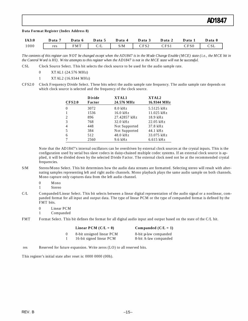
AD1847
REV. B –15–
Data Format Register (Index Address 8)
IA3:0 Data 7 Data 6 Data 5 Data 4 Data 3 Data 2 Data 1 Data 0
1000 res FMT C/L S/M CFS2 CFS1 CFS0 CSL
The contents of this register can NOT be changed except when the AD1847 is in the Mode Change Enable (MCE) state (i.e., the MCE bit inthe Control Word is HI). Write attempts to this register when the AD1847 is not in the MCE state will not be successful.
CSL Clock Source Select. This bit selects the clock source to be used for the audio sample rate.
0 XTAL1 (24.576 MHz)
1 XTAL2 (16.9344 MHz)
CFS2:0 Clock Frequency Divide Select. These bits select the audio sample rate frequency. The audio sample rate depends onwhich clock source is selected and the frequency of the clock source.
Divide XTAL1 XTAL2CFS2:0 Factor 24.576 MHz 16.9344 MHz
0 3072 8.0 kHz 5.5125 kHz1 1536 16.0 kHz 11.025 kHz2 896 27.42857 kHz 18.9 kHz3 768 32.0 kHz 22.05 kHz4 448 Not Supported 37.8 kHz5 384 Not Supported 44.1 kHz6 512 48.0 kHz 33.075 kHz7 2560 9.6 kHz 6.615 kHz
Note that the AD1847’s internal oscillators can be overdriven by external clock sources at the crystal inputs. This is theconfiguration used by serial bus slave codecs in daisy-chained multiple codec systems. If an external clock source is ap-plied, it will be divided down by the selected Divide Factor. The external clock need not be at the recommended crystalfrequencies.
S/M Stereo/Mono Select. This bit determines how the audio data streams are formatted. Selecting stereo will result with alter-nating samples representing left and right audio channels. Mono playback plays the same audio sample on both channels.Mono capture only captures data from the left audio channel.
0 Mono1 Stereo
C/L Companded/Linear Select. This bit selects between a linear digital representation of the audio signal or a nonlinear, com-panded format for all input and output data. The type of linear PCM or the type of companded format is defined by theFMT bits.
0 Linear PCM1 Companded
FMT Format Select. This bit defines the format for all digital audio input and output based on the state of the C/L bit.
Linear PCM (C/L = 0) Companded (C/L = 1)
0 8-bit unsigned linear PCM 8-bit µ-law companded1 16-bit signed linear PCM 8-bit A-law companded
res Reserved for future expansion. Write zeros (LO) to all reserved bits.
This register’s initial state after reset is: 0000 0000 (00h).

AD1847
REV. B–16–
Interface Configuration Register (Index Address 9)
IA3:0 Data 7 Data 6 Data 5 Data 4 Data 3 Data 2 Data 1 Data 0
1001 res res res res ACAL res res PEN
PEN Playback Enable. This bit will enable the playback of data in the format selected. PEN may be set and reset withoutsetting the MCE bit.
0 Playback Disabled1 Playback Enabled
ACAL Autocalibrate Enable. This bit determines whether the AD1847 performs an autocalibrate when exiting from the ModeChange Enable (MCE) state. If the ACAL bit is not set, the previous autocalibration values are used when returning fromthe Mode Change Enable (MCE) state and no autocalibration takes place. Autocalibration must be preformed after initialpower-up for proper operation. This bit is HI after reset.
0 No autocalibration1 Autocalibration allowedNOTE: The ACAL bit can only be changed when the AD1847 is in the Mode Change Enable (MCE) state.
res Reserved for future expansion. Write zeros (LO) to all reserved bits.
This register’s initial state after reset is: 0000 1000 (08h).
Pin Control Register (Index Address 10)
IA3:0 Data 7 Data 6 Data 5 Data 4 Data 3 Data 2 Data 1 Data 0
1010 XCTL1 XCTL0 CLKTS res res res res res
CLKTS Clock Three-State. If the BM bit is HI, and the CLKTS bit is HI, then the CLKOUT pin will be three-stated. If the BMbit is HI, and the bit CLKTS is LO, then the CLKOUT pin is not three-stated. If the BM bit is LO, then the CLKOUTpin is always three-stated.
XCTL1:0 External Control. The state of these independent bits is reflected on the respective XCTL1 and XCTL0 pins of theAD1847.
0 TTL logic LO on XCTL1, XCTL0 pins
1 TTL logic HI on XCTL1, XCTL0 pins
res Reserved for future expansion. Write zeros (LO) to all reserved bits.
This register’s initial state after reset is: 0000 0000 (00h).
Invalid Address (Index Address 11)
IA3:0 Data 7 Data 6 Data 5 Data 4 Data 3 Data 2 Data 1 Data 0
1011 inval inval inval inval inval inval inval inval
inval Writes to this index address are ignored. Index readback of this index address will return the Status Word.

AD1847
REV. B –17–
Miscellaneous Information Register (Index Address 12)
IA3:0 Data 7 Data 6 Data 5 Data 4 Data 3 Data 2 Data 1 Data 0
1100 FRS TSSEL res res res res res res
The Miscellaneous Information Register can only be changed when the AD1847 is in the Mode Change Enable (MCE) state. Changes to thisregister are updated at the next Serial Data Frame Sync (SDFS) boundary. If FRS is LO (i.e., 32 slots per frame), and either TSSEL or FRSchange in the first sample of a frame, the change is not updated at the second sample of the same frame, but at the first sample of the next frame.
TSSEL Transmit Slot Select. This bit determines which TDM time slots the AD1847 should transmit on.0 Transmit on time slots 3, 4 and 5. Used when SDI and SDO are tied together (i.e., “1-wire” system).1 Transmit on slots 0, 1 and 2. Used when SDI and SDO are independent inputs and outputs
(i.e., “2-wire” system).
FRS Frame Size. This bit selects the number of time slots per frame.0 Selects 32 slots per frame (two samples per frame sync or frame sync at half the sample rate).1 Selects 16 slots per frame (one sample per frame sync or frame sync at the sample rate).
res Reserved for future expansion. Write zeros (LO) to all reserved bits.
This register’s initial state after reset is: 0000 0000 (00h).
Digital Mix Control Register (Index Address 13)
IA3:0 Data 7 Data 6 Data 5 Data 4 Data 3 Data 2 Data 1 Data 0
1101 DMA5 DMA4 DMA3 DMA2 DMA1 DMA0 res DME
DME Digital Mix Enable. This bit enables the digital mix of the ADCs’ output with the DACs’ input. When enabled, the datafrom the ADCs is digitally mixed with other data being delivered to the DACs (regardless of whether or not playback[PEN] is enabled, i.e., set). If there is a capture overrun, then the last sample captured before overrun will be used forthe digital mix. If playback is enabled (PEN set) and there is a playback underrun, then a midscale zero will be added tothe digital mix data.
0 Digital mix disabled (muted)1 Digital mix enabled
DMA5:0 Digital Mix Attenuation. These bits determine the attenuation of the ADC output data mixed with the DAC input data.The least significant bit of this 64-level attenuate select represents –1.5 dB. Maximum attenuation is –94.5 dB.
res Reserved for future expansion. Write zeros (LO) to all reserved bits.
This register’s initial state after reset is: 0000 0000 (00h).
Invalid Address (Index Address 14)
IA3:0 Data 7 Data 6 Data 5 Data 4 Data 3 Data 2 Data 1 Data 0
1110 inval inval inval inval inval inval inval inval
inval Writes to this index address are ignored. Index readback of this index address will return the Status Word.
Invalid Address (Index Address 15)
IA3:0 Data 7 Data 6 Data 5 Data 4 Data 3 Data 2 Data 1 Data 0
1111 inval inval inval inval inval inval inval inval
inval Writes to this index address are ignored. Index readback of this index address will return the Status Word.

AD1847
REV. B–18–
Serial Data InterfaceThe AD1847 serial data interface uses a Time Division Multi-plex (TDM) scheme that is compatible with DSP serial portsconfigured in Multi-Channel Mode with either 32 or 16 16-bittime slots. An AD1847 is always the serial bus master, transmit-ting the serial clock (SCLK) and the serial data frame sync(SDFS). The AD1847 always receives control and playbackdata in time slots 0, 1 and 2. The AD1847 will transmit statusor index register readback and capture data in time slots 0, 1and 2 if TSSEL = 1, and will transmit status or index registerreadback and capture data in time slots 3, 4 and 5 if TSSEL =0. The following table in Figure 7 shows an example of how thetime slots might be assigned.
In this example design, which uses the ADSP-21xx DSP, eachframe is divided into 32 time slots of 16-bits each (FRS = 0).Two audio samples are contained in the 32 time slots, with asingle frame sync (SDFS) at the beginning of the frame. TheADSP-21xx serial port (SPORT0) supports 32 time slots. Theformat of the first 16 time slots (sample N) is the same as theformat of the second 16 time slots (sample N+1). In this ex-ample, 24 time slots are used, as indicated below. Note thattime slots 12 through 15 and 28 through 31 are unused in thisexample, and that Figure 7 presumes that TSSEL = 0 (“1-wire”system).
Slot Number Source Destination Format
0, 16 AD1847 Control Word1, 17 ASIC AD1847 Left Playback Data2, 18 Right Playback Data3, 19 AD1847 Status Word/
Index Readback4, 20 AD1847 ASIC Left Capture Data5, 21 Right Capture Data0, 16 AD1847 Control Word1, 17 DSP AD1847 Left Playback Data2, 18 Right Playback Data3, 19 AD1847 Status Word/
Index Readback4, 20 AD1847 DSP Left Capture Data5, 21 Right Capture Data6, 22 DSP Control7, 23 ASIC DSP Left Processed
Playback Data8, 24 Right Processed
Playback Data9, 25 DSP Status10, 26 DSP ASIC Left Processed
Capture Data
11, 27 Right ProcessedCapture Data
Figure 7. Time Slot Assignment Example
Note that in this “1-wire” system example, the Digital SignalProcessor (DSP) and ISA Bus Interface ASIC (ASIC) use thesame slots to communicate to the AD1847. This reduces thenumber of total time slots required and eliminates the need forthe AD1847 to distinguish between DSP data and ASIC data.Also, in this example the ASIC and the DSP do not send data tothe AD1847 at the same time, so separate slots are unnecessary.
The digital data in the serial interface is pipelined up to 2samples deep. This pipelining is required to properly resolve theinterface between the relatively fast fixed SCLK rate, and therelatively slow sample rates (and therefore frame sync rates) atwhich the AD1847 is capable of running. At low sample rates,two samples of data can be serviced in a fraction of a sample pe-riod. For example, at an 8 kHz sample rate, 32 time slots onlyconsume 32 × 16 × (1/12.288 MHz) = 41.67 µs out of a 125 µsperiod. The two-deep data pipeline thus allows sample overrun(capture) and sample underrun (playback) to be avoided.
Figure 8 represents a logical view of the slot utilization betweendevices.
AD1847SDI
SDO
0, 1, 2, 16, 17, 18
ASIC
ADSP-21XX
DR
DT
DT
DR
NOTE: DSP MUST HAVE TWO SERIAL PORTS
6, 7, 8,22, 23, 24
9, 10, 11,25, 26, 27
3, 4, 5, 19, 20, 21
0, 1, 2,16, 17, 18
3, 4, 5, 19, 20, 21
Figure 8. Time Slot Allocation Example
Note that this is a system specific 1-wire example. For non-DSPoperation, the DSP is either not present or disabled. If the DSPis present, the ASIC configures the DSP through slot 6 (and slot22) to three-state its outputs in time slots 0, 1 and 2 (and slots16, 17 and 18). The ASIC can then enable its drivers for timeslots 0, 1 and 2 (and slots 16, 17 and 18). For DSP operation,the ASIC three-states its outputs for time slots 0, 1 and 2 (andslots 16, 17 and 18) and enables the DSP drivers for slots 0, 1and 2 (and slots 16, 17, and 18).
An application note is available from Analog Devices with addi-tional information on interfacing to the AD1847 serial port.This application note can be obtained through your local Ana-log Devices representative, or downloaded from the DSP Bulle-tin Board Service at (617) 461-4258 (8 data bits, no parity, 1stop bit, 300/1200/2400/4600 baud).

AD1847
REV. B –19–
Control Word
Data 15 Data 14 Data 13 Data 12 Data 11 Data 10 Data 9 Data 8
CLOR MCE RREQ res IA3 IA2 IA1 IA0
Data 7 Data 6 Data 5 Data 4 Data 3 Data 2 Data 1 Data 0
DATA7 DATA6 DATA5 DATA4 DATA3 DATA2 DATA1 DATA0
Left Playback Data
Data 15 Data 14 Data 13 Data 12 Data 11 Data 10 Data 9 Data 8
DATA15 DATA14 DATA13 DATA12 DATA11 DATA10 DATA9 DATA8
Data 7 Data 6 Data 5 Data 4 Data 3 Data 2 Data 1 Data 0
DATA7 DATA6 DATA5 DATA4 DATA3 DATA2 DATA1 DATA0
Right Playback Data
Data 15 Data 14 Data 13 Data 12 Data 11 Data 10 Data 9 Data 8
DATA15 DATA14 DATA13 DATA12 DATA11 DATA10 DATA9 DATA8
Data 7 Data 6 Data 5 Data 4 Data 3 Data 2 Data 1 Data 0
DATA7 DATA6 DATA5 DATA4 DATA3 DATA2 DATA1 DATA0
Status Word
Data 15 Data 14 Data 13 Data 12 Data 11 Data 10 Data 9 Data 8
res res RREQ res ID3 ID2 ID1 ID0
Data 7 Data 6 Data 5 Data 4 Data 3 Data 2 Data 1 Data 0
res res ORR1 ORR0 ORL1 ORL0 ACI INIT
Index Readback
Data 15 Data 14 Data 13 Data 12 Data 11 Data 10 Data 9 Data 8
CLOR MCE RREQ res IA3 IA2 IA1 IA0
Data 7 Data 6 Data 5 Data 4 Data 3 Data 2 Data 1 Data 0
DATA7 DATA6 DATA5 DATA4 DATA3 DATA2 DATA1 DATA0
Left Capture Data
Data 15 Data 14 Data 13 Data 12 Data 11 Data 10 Data 9 Data 8
DATA15 DATA14 DATA13 DATA12 DATA11 DATA10 DATA9 DATA8
Data 7 Data 6 Data 5 Data 4 Data 3 Data 2 Data 1 Data 0
DATA7 DATA6 DATA5 DATA4 DATA3 DATA2 DATA 1 DATA0
Right Capture Data
Data 15 Data 14 Data 13 Data 12 Data 11 Data 10 Data 9 Data 8
DATA15 DATA14 DATA13 DATA12 DATA11 DATA10 DATA9 DATA8
Data 7 Data 6 Data 5 Data 4 Data 3 Data 2 Data 1 Data 0
DATA7 DATA6 DATA5 DATA4 DATA3 DATA2 DATA1 DATA0
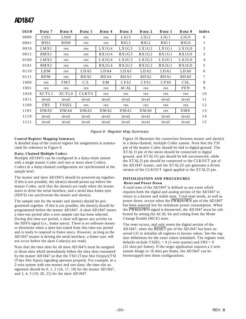
AD1847
REV. B–20–
IA3:0 Data 7 Data 6 Data 5 Data 4 Data 3 Data 2 Data 1 Data 0 Index
0000 LSS1 LSS0 res res LIG3 LIG2 LIG1 LIG0 0
0001 RSS1 RSS0 res res RIG3 RIG2 RIG1 RIG0 1
0010 LMX1 res res LX1G4 LX1G3 LX1G2 LX1G1 LX1G0 2
0011 RMX1 res res RX1G4 RX1G3 RX1G2 RX1G1 RX1G0 3
0100 LMX2 res res LX2G4 LX2G3 LX2G2 LX2G1 LX2G0 4
0101 RMX2 res res RX2G4 RX2G3 RX2G2 RX2G1 RX2G0 5
0110 LDM res LDA5 LDA4 LDA3 LDA2 LDA1 LDA0 6
0111 RDM res RDA5 RDA4 RDA3 RDA2 RDA1 RDA0 7
1000 res FMT C/L S/M CFS2 CFS1 CFS0 CSL 8
1001 res res res res ACAL res res PEN 9
1010 XCTL1 XCTL0 CLKTS res res res res res 10
1011 inval inval inval inval inval inval inval inval 11
1100 FRS TSSEL res res res res res res 12
1101 DMA5 DMA4 DMA3 DMA2 DMA1 DMA0 res DME 13
1110 inval inval inval inval inval inval inval inval 14
1111 inval inval inval inval inval inval inval inval 15
Figure 9. Register Map Summary
Control Register Mapping SummaryA detailed map of the control register bit assignments is summa-rized for reference in Figure 9.
Daisy-Chained Multiple CodecsMultiple AD1847s can be configured in a daisy-chain systemwith a single master Codec and one or more slave Codecs.Codecs in a daisy-chained configuration are synchronized at thesample level.
The master and slave AD1847s should be powered-up together.If this is not possible, the slave(s) should power-up before themaster Codec, such that the slave(s) are ready when the masterstarts to drive the serial interface, and a serial data frame sync(SDFS) can synchronize the master and slave(s).
The sample rate for the master and slave(s) should be pro-grammed together. If this is not possible, the slave(s) should beprogrammed before the master AD1847. A slave AD1847 entersa time-out period after a new sample rate has been selected.During this time-out period, a slave will ignore any activity onthe SDFS signal (i.e., frame syncs). There is no software meansto determine when a slave has exited from this time-out periodand is ready to respond to frame syncs. However, as long as theAD1847 master is driving the serial interface, a frame sync willnot occur before the slave Codec(s) are ready.
Note that the time slots for all slave AD1847s must be assignedto those slots which immediately follow the time slots consumedby the master AD1847 so that the TSO (Time Slot Output)/TSI(Time Slot Input) signaling operates properly. For example, in a2-wire system with one master and one slave, the time slot as-signment should be 0, 1, 2 (16, 17, 18) for the master AD1847,and 3, 4, 5 (19, 20, 21) for the slave AD1847.
Figure 10 illustrates the connection between master and slave(s)in a daisy-chained, multiple Codec system. Note that the TSIpin of the master Codec should be tied to digital ground. TheXTAL1I pin of the slaves should be connected to digitalground, and XTAL1O pin should be left unconnected, whilethe XTAL2I pin should be connected to the CLKOUT pin ofthe AD1847 master, and the XTAL2O pin generates a drivenversion of the CLKOUT signal applied to the XTAL2I pin.
INITIALIZATION AND PROCEDURES Reset and Power DownA total reset of the AD1847 is defined as any event whichrequires both the digital and analog section of the AD1847 toreturn to a known and stable state. Total reset mode, as well aspower down, occurs when the PWRDOWN pin of the AD1847has been asserted low for minimum power consumption. Whenthe PWRDOWN signal is deasserted, the AD1847 must be cali-brated by setting the ACAL bit and exiting from the ModeChange Enable (MCE) state.
The reset occurs, and only resets the digital section of theAD1847, when the RESET pin of the AD1847 has been as-serted LO to initialize all registers to known values. See the reg-ister definitions for the exact values initialized. The register resetdefaults include TSSEL = 0 (1-wire system) and FRS = 0(32 slots per frame). If the target application requires a 2-wiresystem design or 16 slots per frame, the AD1847 can bebootstrapped into these configurations.
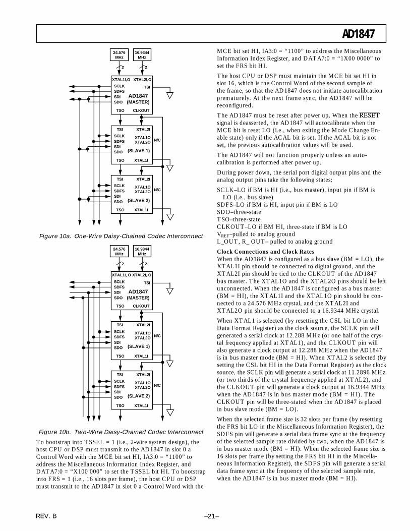
AD1847
REV. B –21–
2
XTAL1I,O XTAL2I,O
TSO CLKOUT
AD1847(MASTER)
2
SCLKSDFSSDISDO
16.9344MHz
24.576MHz
TSI
TSI XTAL2I
TSO XTAL1I
(SLAVE 1)
SCLKSDFSSDISDO
XTAL1OXTAL2O N/C
TSI XTAL2I
TSO XTAL1I
(SLAVE 2)
SCLKSDFSSDISDO
XTAL1OXTAL2O N/C
Figure 10a. One-Wire Daisy-Chained Codec Interconnect
2
XTAL1I, O XTAL2I, O
TSO CLKOUT
AD1847(MASTER)
2
SCLKSDFSSDISDO
16.9344MHz
24.576MHz
TSI
TSI XTAL2I
TSO XTAL1I
(SLAVE 1)
SCLKSDFSSDISDO
XTAL1OXTAL2O N/C
TSI XTAL2I
TSO XTAL1I
(SLAVE 2)
SCLKSDFSSDISDO
XTAL1OXTAL2O N/C
Figure 10b. Two-Wire Daisy-Chained Codec Interconnect
To bootstrap into TSSEL = 1 (i.e., 2-wire system design), thehost CPU or DSP must transmit to the AD1847 in slot 0 aControl Word with the MCE bit set HI, IA3:0 = “1100” toaddress the Miscellaneous Information Index Register, andDATA7:0 = “X100 000” to set the TSSEL bit HI. To bootstrapinto FRS = 1 (i.e., 16 slots per frame), the host CPU or DSPmust transmit to the AD1847 in slot 0 a Control Word with the
MCE bit set HI, IA3:0 = “1100” to address the MiscellaneousInformation Index Register, and DATA7:0 = “1X00 0000” toset the FRS bit HI.
The host CPU or DSP must maintain the MCE bit set HI inslot 16, which is the Control Word of the second sample ofthe frame, so that the AD1847 does not initiate autocalibrationprematurely. At the next frame sync, the AD1847 will bereconfigured.
The AD1847 must be reset after power up. When the RESETsignal is deasserted, the AD1847 will autocalibrate when theMCE bit is reset LO (i.e., when exiting the Mode Change En-able state) only if the ACAL bit is set. If the ACAL bit is notset, the previous autocalibration values will be used.
The AD1847 will not function properly unless an auto-calibration is performed after power up.
During power down, the serial port digital output pins and theanalog output pins take the following states:
SCLK–LO if BM is HI (i.e., bus master), input pin if BM isLO (i.e., bus slave)
SDFS–LO if BM is HI, input pin if BM is LOSDO–three-stateTSO–three-stateCLKOUT–LO if BM HI, three-state if BM is LOVREF–pulled to analog groundL_OUT, R_ OUT– pulled to analog ground
Clock Connections and Clock RatesWhen the AD1847 is configured as a bus slave (BM = LO), theXTAL1I pin should be connected to digital ground, and theXTAL2I pin should be tied to the CLKOUT of the AD1847bus master. The XTAL1O and the XTAL2O pins should be leftunconnected. When the AD1847 is configured as a bus master(BM = HI), the XTAL1I and the XTAL1O pin should be con-nected to a 24.576 MHz crystal, and the XTAL2I andXTAL2O pin should be connected to a 16.9344 MHz crystal.
When XTAL1 is selected (by resetting the CSL bit LO in theData Format Register) as the clock source, the SCLK pin willgenerated a serial clock at 12.288 MHz (or one half of the crys-tal frequency applied at XTAL1), and the CLKOUT pin willalso generate a clock output at 12.288 MHz when the AD1847is in bus master mode (BM = HI). When XTAL2 is selected (bysetting the CSL bit HI in the Data Format Register) as the clocksource, the SCLK pin will generate a serial clock at 11.2896 MHz(or two thirds of the crystal frequency applied at XTAL2), andthe CLKOUT pin will generate a clock output at 16.9344 MHzwhen the AD1847 is in bus master mode (BM = HI). TheCLKOUT pin will be three-stated when the AD1847 is placedin bus slave mode (BM = LO).
When the selected frame size is 32 slots per frame (by resettingthe FRS bit LO in the Miscellaneous Information Register), theSDFS pin will generate a serial data frame sync at the frequencyof the selected sample rate divided by two, when the AD1847 isin bus master mode (BM = HI). When the selected frame size is16 slots per frame (by setting the FRS bit HI in the Miscella-neous Information Register), the SDFS pin will generate a serialdata frame sync at the frequency of the selected sample rate,when the AD1847 is in bus master mode (BM = HI).

AD1847
REV. B–22–
When the AD1847 is in bus slave mode (BM = LO), the TSIpin should be connected to the TSO pin of the AD1847 masteror slave which has been assigned to the preceding time slots.The signal on the TSO pin is essentially the signal received onthe TSI pin, but delayed by 3 or 6 time slots from TSI (depend-ing on the state of TSSEL). The frequency of the transitions onthe TSI and TSO lines is equivalent to the frequency on theSDFS pin.
When the AD1847 is in bus master mode (BM = HI), the TSIpin should be connected to digital ground. The signal on theTSO pin is essentially the same as the signal output on theSDFS pin, but delayed by 3 or 6 time slots from SDFS (again,depending on the state of TSSEL).
Mode Change Enable StateThe AD1847 must be in the Mode Change Enable (MCE) statebefore any changes to the ACAL bit of the Interface Configura-tion Register, the Data Format Register, or the MiscellaneousInformation Register are allowed. Note that the MCE bit doesnot have to be reset LO in order for changes to take effect.
Digital MixDigital mix is enabled via the DME bit in the Digital Mix Con-trol Register. The digital mix routes the digital data from theADCs to the DACs. The mix can be digitally attenuated via bitsalso in the Digital Mix Control Register. The ADC data issummed with the DAC data supplied at the digital bus inter-face. When digital mix is enabled and the PEN bit is not set,ADC data is summed with zeros to produce the DAC output.
If the sum of the digital mix (ADC output and DAC input fromthe serial bus interface) is greater than full scale, the AD1847will send a positive or negative full scale value to the DACs,whichever is appropriate (clipping).
AutocalibrationThe AD1847 has the ability to calibrate its ADCs and DACs forgreater accuracy by minimizing dc offsets. Autocalibration oc-curs whenever the AD1847 exits from the Mode Change Enable(MCE) state AND the ACAL bit in the Interface ConfigurationRegister has been set.
The completion of the autocalibration sequence can be deter-mined by polling the Autocalibration In-Progress (ACI) bit inthe Status Word. This bit will be HI while the autocalibration isin progress and LO once autocalibration has completed. Theautocalibration sequence will take at least 384 sample periods.
The autocalibration procedure is as follows:
1. Mute both left and right AUX1 and AUX2 inputs via the LeftAuxiliary Input and Right Auxiliary Input Control Registers.
2. Place the AD1847 in the Mode Change Enable (MCE) stateusing the MCE bit of the AD1847 Control Word. Set theACAL bit in the Interface Configuration Register.
3. Exit from the Mode Change Enable state by resetting theMCE bit.
4. Poll the ACI bit in the AD1847 Status Word for a HI(autocalibration in progress), then poll the ACI bit for a LO(autocalibration complete).
5. Unmute the AUX inputs, if used.
If ACAL is not set, the AD1847 is muted for 128 sample peri-ods after resetting the MCE bit, and the ACI bit in the StatusWord is set HI during this 128 sample periods. Autocalibrationmust be performed after power-up to ensure proper operation ofthe AD1847.
Exiting from the MCE state always causes ACI to go HI. If theACAL bit is set when MCE state is exited, then the ACI bit willbe HI for 384 sample periods. If the ACAL bit is reset whenMCE is exited, then the ACI bit will be HI for 128 sampleperiods.
Changing Sample RatesThe internal states of the AD1847 are synchronized by theselected sample frequency defined in the Data Format Register.The changing of either the clock source or the clock frequencydivide requires a special sequence for proper AD1847 operation.
1. Mute the outputs of the AD1847 and enter the Mode ChangeEnable (MCE) state by setting the MCE bit of the AD1847Control Word.
2. During a single atomic or nondivisible write cycle, change theClock Frequency Divide Select (CFS) and/or the ClockSource Select (CSL) bits of the Data Format Register to thedesired values. CFS and CSL can be programmed in thesame Control Word as MCE.
3. The INIT bit in the Status Word will be set HI at the lastsample of the next frame to indicate that the serial port will bedisabled for a timeout period.
4. The AD1847 requires a period of time to resynchronize itsinternal states to the newly selected clock. During this time,the AD1847 will be unable to respond at its serial interfaceport (i.e., no frame syncs will be generated). The time-outperiod is 221 3 SCLK ≈ 170 ms after power-up, and ≈ 5 msfor subsequent changes of sample rate.
5. Exit the Mode Change Enable state by resetting the MCE bit.Upon exiting the MCE state, an autocalibration of duration384 sample periods or an output mute of duration 128 sampleperiods occurs, depending on the state of the ACAL bit.
6. Poll the ACI bit in the AD1847 Status Word for a HI (indi-cating that autocalibration is in progress) then poll the ACIbit for a LO (indicating that autocalibration has completed).Once the ACI bit has been read back LO, normal operation ofthe Codec can resume.
The CSL and CFS bits cannot be changed unless the AD1847is in the Mode Change Enable state (i.e., the MCE bit in theAD1847 Control Word is set). Attempts to change the contentsof the Data Format Register without MCE set will result in thewrite cycle not being recognized (the bits will not be updated).
The MCE bit should not be reset until after the INIT bit in theAD1847 Status Word is detected HI. After the INIT bit is de-tected HI, the serial port is disabled. When the next frame syncarrives (after the time-out period), all internal clocks are stableand the serial port is ready for normal operation.

AD1847
REV. B –23–
DATA FORMAT DEFINITIONSThere are four data formats supported by the AD1847: 16-bitsigned, 8-bit unsigned, 8-bit companded µ-law, and 8-bit com-panded A-law. The AD1847 supports these four formats becauseeach of them have found wide use in important applications.
16-Bit Signed FormatThe 16-bit signed format (also called 16-bit twos-complement)is the standard method of representing 16-bit digital audio. Thisformat yields 96 dB of dynamic range and is common in con-sumer compact disk audio players. This format uses the value– 32768 (8000h) to represent minimum analog amplitude while32767 (7FFFh) represents maximum analog amplitude. Inter-mediate values are a linear interpolation between minimum andmaximum amplitude values.
MAX
MIN8000h
DIGITAL VALUE
AN
AL
OG
VA
LU
E
0000h 7FFFh
Figure 11. 16-Bit Signed Format
8-Bit Unsigned FormatThe 8-bit unsigned format is commonly used in the personalcomputer industry. This format delivers 48 dB of dynamicrange. The value 0 (00h) is used to represent minimum analogamplitude while 255 (FFh) is used to represent maximum ana-log amplitude. Intermediate values are a linear interpolation be-tween minimum and maximum amplitude values. The leastsignificant byte of the 16-bit internal data is truncated to createthe 8-bit output samples.
MAX
MIN00h
DIGITAL VALUE
AN
AL
OG
VA
LU
E
7Fh FFh
Figure 12. 8-Bit Unsigned Format
8-Bit Companded FormatsThe 8-bit companded formats (µ-law and A-law) are used in thetelecommunications industry. Both of these formats are used inISDN communications and workstations; µ-law is the standardfor the United States and Japan while A-law is used in Europe.Companded audio allows either 64 dB or 72 dB of dynamicrange using only 8-bits per sample. This is accomplished using anonlinear formula which assigns more digital codes to lower am-plitude analog signals at the expense of resolution of higher am-plitude signals. The µ-law format of the AD1847 conforms tothe Bell System µ = 255 companding law while the A-law formatconforms to CCITT “A” law models. Figure 13 shows approxi-mately how both the µ-law and A-law companding schemes be-have. Refer to the standards mentioned above for an exactdefinition.
MAX
MIN00h FFh 80h
AAh
µ-law
A-lawD5h2Ah
DIGITAL VALUE
AN
AL
OG
VA
LU
E
Figure 13. 8-Bit Companded Format
APPLICATIONS CIRCUITSThe AD1847 Stereo Codec has been designed to require a mini-mum of external circuitry. The recommended circuits are shownin Figures 14 through 22. Analog Devices estimates that the to-tal cost of all the components shown in these Figures, includingcrystals, to be less than $3 in 10,000 quantities.
Industry-standard compact disc “line-levels” are 2 Vrms centeredaround analog ground. (For other audio equipment, “line level”is much more loosely defined.) The AD1847 SoundPort is a+5 V only powered device. Line level voltage swings for theAD1847 are defined to be 1 Vrms for a sine wave ADC input and0.707 Vrms for a sine wave DAC output. Thus, 2 Vrms input ana-log signals must be attenuated and either centered around thereference voltage intermediate between 0 V and +5 V orac-coupled. The VREF pin will be at this intermediate voltage,nominally 2.25 V. It has limited drive but can be used as a volt-age datum to an op amp input. Note, however, that dc-coupledinputs are not recommended, as they provide no performancebenefits with the AD1847 architecture. Furthermore, dc offsetdifferences between multiple dc-coupled inputs create the po-tential for “clicks” when changing the input mux selection.

AD1847
REV. B–24–
Circuits for 2 Vrms line-level inputs and auxiliaries are shown inFigure 14 and Figure 15. Note that these are divide-by-tworesistive dividers. The input resistor and 560 pF (1000 pF)capacitor provide the single-pole of antialias filtering requiredfor the ADCs. If line-level inputs are already at the 1 Vrms levelsexpected by the AD1847, the resistors in parallel with the560 pF (1000 pF) capacitors can be omitted. If the applicationdoes not route the AUX2 inputs to the ADCs, then no antialiasfiltering is required (only the 1 µF ac coupling capacitor).
5.1k
560pFNPO
5.1k
0.33 µFR_LINE1R_LINE2
5.1k
560pFNPO
5.1k
0.33 µFL_LINE1L_LINE2
Figure 14. 2 Vrms Line-Level Input Circuit for Line Inputs
3.3k
1000pFNPO
4.3k
L_AUX1L_AUX2
1µF
R_AUX1R_AUX2
3.3k
1000pFNPO
4.3k
1µF
Figure 15. 2 Vrms Line-Level Input Circuit for AUX Inputs
Figure 16 illustrates one example of how an electret condensermicrophone requiring phantom power could be connected tothe AD1847. VREF is shown buffered by an op amp; a transistorlike a 2N4124 will also work well for this purpose. Note that if abattery-powered microphone is used, the buffer and R2s are notneeded. The values of R1, R2, and C should be chosen in lightof the mic characteristics and intended gain. Typical values forthese might be R1 = 20 kΩ, R2 = 2 kΩ, and C = 220 pF.
1/2 SSM2135OR AD820
R2
R2
LEFTELECTRET
CONDENSERMICROPHONE
INPUT
5k 0.33µFL_LINE1L_LINE2
1µF
R1
C
1/2 SSM2135OR AD820
VREF
5k 0.33µFR_LINE1R_LINE2
1µFR1
C
1/2 SSM2135OR AD820
VREF
RIGHTELECTRET
CONDENSERMICROPHONE
INPUT
Figure 16. “Phantom-Powered” Microphone Input Circuit
Figure 17 shows ac-coupled line outputs. The resistors areused to center the output signals around analog ground. Ifdc-coupling is desired, VREF could be used with op amps asmentioned previously.
47k
1µFL_OUT
47k
1µFR_OUT
Figure 17. Line Output Connections
A circuit for headphone drive is illustrated in Figure 18. Drive issupplied by +5 V operational amps. The circuit shown accouples the headphones to the line output.
SSM2135
20k 470µF
18k
VREF
HEADPHONELEFT
20k470µF
18k
HEADPHONERIGHT
L_OUT
R_OUT
Figure 18. Headphone Drive Connections
Figure 19 illustrates reference bypassing. VREFI should only beconnected to its bypass capacitors.
10µF 0.1µF
VREFI
10µF
VREF
Figure 19. Voltage Reference Bypassing
Figure 20 illustrates signal-path filtering capacitors, L_FILTand R_FILT. The AD1847 must use 1.0 µF capacitors. The1.0 µF capacitors required by the AD1847 can be of any type.
1.0µF
LFILT
1.0µF
RFILT
Figure 20. External Filter Capacitor Connections
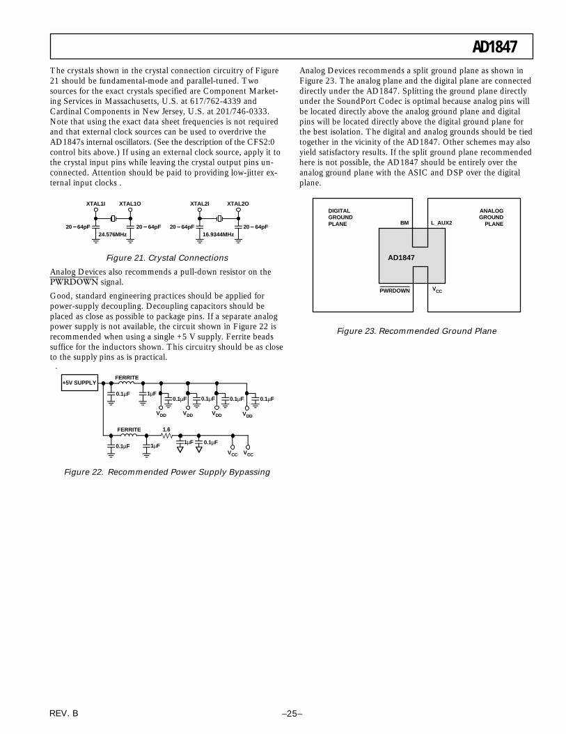
AD1847
REV. B –25–
The crystals shown in the crystal connection circuitry of Figure21 should be fundamental-mode and parallel-tuned. Twosources for the exact crystals specified are Component Market-ing Services in Massachusetts, U.S. at 617/762-4339 andCardinal Components in New Jersey, U.S. at 201/746-0333.Note that using the exact data sheet frequencies is not requiredand that external clock sources can be used to overdrive theAD1847s internal oscillators. (See the description of the CFS2:0control bits above.) If using an external clock source, apply it tothe crystal input pins while leaving the crystal output pins un-connected. Attention should be paid to providing low-jitter ex-ternal input clocks .
XTAL1I XTAL1O
20 64pF 20 64pF24.576MHz
XTAL2I XTAL2O
20 64pF 20 64pF16.9344MHz
Figure 21. Crystal Connections
Analog Devices also recommends a pull-down resistor on thePWRDOWN signal.
Good, standard engineering practices should be applied forpower-supply decoupling. Decoupling capacitors should beplaced as close as possible to package pins. If a separate analogpower supply is not available, the circuit shown in Figure 22 isrecommended when using a single +5 V supply. Ferrite beadssuffice for the inductors shown. This circuitry should be as closeto the supply pins as is practical.
+5V SUPPLY
0.1µF
FERRITE
1µF0.1µF
VDD VDD VDD
0.1µF
VDD
0.1µF
FERRITE
1µF
1.6
0.1µF1µF
VCC VCC
0.1µF 0.1µF
Figure 22. Recommended Power Supply Bypassing
Analog Devices recommends a split ground plane as shown inFigure 23. The analog plane and the digital plane are connecteddirectly under the AD1847. Splitting the ground plane directlyunder the SoundPort Codec is optimal because analog pins willbe located directly above the analog ground plane and digitalpins will be located directly above the digital ground plane forthe best isolation. The digital and analog grounds should be tiedtogether in the vicinity of the AD1847. Other schemes may alsoyield satisfactory results. If the split ground plane recommendedhere is not possible, the AD1847 should be entirely over theanalog ground plane with the ASIC and DSP over the digitalplane.
DIGITALGROUNDPLANE
ANALOGGROUND
PLANE
PWRDOWN VCC
BM L_AUX2
AD1847
Figure 23. Recommended Ground Plane

AD1847
REV. B–26–
FREQUENCY RESPONSE PLOTS
10
–1201.0
–90
–110
0.1
–100
0.0
–60
–80
–70
–50
–30
–20
0
–10
–40
0.8 0.90.70.60.50.40.30.2
dB
SAMPLE FREQUENCY – FS
Figure 24. AD1847 Analog-to-Digital Frequency Response(Full-Scale Line-Level Inputs, 0 dB Gain)
dB
SAMPLE FREQUENCY – FS
10
–1200.70
–90
–110
–100
0.40
–60
–80
–70
–50
–30
–20
0
–10
–40
0.64 0.680.600.560.520.480.44
Figure 25. AD1847 Analog-to-Digital Frequency Response–Transition Band (Full-Scale Line-Level Inputs, 0 dB Gain)
10
–120
–90
–110
–100
–60
–80
–70
–50
–30
–20
0
–10
–40
1.00.10.0 0.8 0.90.70.60.50.40.30.2
dB
SAMPLE FREQUENCY – FS
Figure 26. AD1847 Digital-to-Analog Frequency Response(Full-Scale Inputs, 0 dB Attenuation)
dB
SAMPLE FREQUENCY – FS
10
–120
–90
–110
–100
–60
–80
–70
–50
–30
–20
0
–10
–40
0.700.40 0.64 0.680.600.560.520.480.44
Figure 27. AD1847 Digital-to-Analog Frequency Response–Transition Band (Full-Scale Inputs, 0 dB Attenuation)

AD1847
REV. B –27–
tHZtDV
tPD1
tS
tH
SCLK
SDFS
SDI
SDO
BIT 15
BIT 14
BIT 0
BIT 15
BIT 14
BIT 0
Figure 28. Time Slot Timing Diagram
SCLK
SDFS
SDI orSDO
TSO
15 3 2 1 0 15 14 13
tPD1
LAST VALID TIME SLOT
tPD2
14 13
Figure 29. TSO Timing Diagram
tRPWLRESET
PWRDOWN
Figure 30. Reset and Power Down Timing Diagram
16-BITSTEREO
8-BITSTEREO
SCLK
SDFS
16-BITMONO
8-BITMONO
CONTROL LEFTPB
SDI/
SDO
TIMESLOT 0
TIMESLOT 1
TIMESLOT 2
CONTROL
STATUS
RIGHTPLAYBACK
RIGHTPLAYBACK
LEFTPLAYBACK
LEFTCAPTURE
CONTROL
STATUS LEFTCAPTURE
LEFTPLAYBACK
LEFTCAPTURE
SDI/
SDO
SDI/
SDO 0LEFTCAPSTATUS
RIGHTPB
RIGHTCAP 0
CONTROL LEFTPBSDI/
SDO 0LEFTCAPSTATUS LEFT
CAP 0
Figure 31. Serial Data Format, 2-Wire System (TSSEL = 1)
16-BITSTEREO
8-BITSTEREO
SCLK
SDFS
TIMESLOT 0
TIMESLOT 1
TIMESLOT 2
TIMESLOT 3
TIMESLOT 4
TIMESLOT 5
16-BITMONO
8-BITMONO
CONTROL LEFT RIGHT STATUS LEFT RIGHT
CONTROL LEFT STATUS LEFT
PLAYBACK CAPTURE
CONTROL LEFT STATUS LEFT
CONTROL LEFT RIGHT STATUS LEFT RIGHT0 0
0 LEFT0
LEFT
SDI/SDO
SDI/SDO
SDI/SDO
SDI/SDO
Figure 32. Serial Data Format, 1-Wire System (TSSEL = 0)
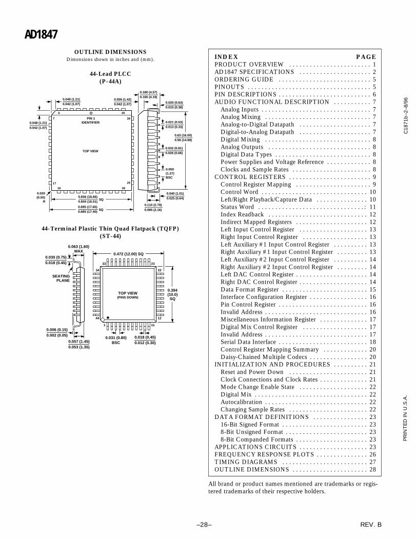
AD1847
REV. B–28–
OUTLINE DIMENSIONSDimensions shown in inches and (mm).
44-Lead PLCC(P-44A)
0.032 (0.81)0.026 (0.66)
0.021 (0.53)0.013 (0.33)
0.056 (1.42)0.042 (1.07) 0.025 (0.63)
0.015 (0.38)
0.180 (4.57)0.165 (4.19)
0.63 (16.00)0.59 (14.99)
0.110 (2.79)
0.085 (2.16)
0.040 (1.01)0.025 (0.64)
0.050(1.27)BSC
0.656 (16.66)0.650 (16.51)
SQ
0.695 (17.65)0.685 (17.40)
SQ
0.048 (1.21)0.042 (1.07)
0.048 (1.21)
0.042 (1.07)
40 6
TOP VIEW
39
29
18
17
PIN 1IDENTIFIER
7
28
0.020(0.50)
R
44-Terminal Plastic Thin Quad Flatpack (TQFP)(ST-44)
TOP VIEW(PINS DOWN)
1
33
34
44
11
12
23
22
0.018 (0.45)0.012 (0.30)
0.031 (0.80)BSC
0.394(10.0)
SQ
0.472 (12.00) SQ
0.057 (1.45)0.053 (1.35)
0.006 (0.15)0.002 (0.05)
SEATINGPLANE
0.063 (1.60)MAX
0.030 (0.75)0.018 (0.45)
C18
71b
–2–8
/96
PR
INT
ED
IN U
.S.A
.
INDEX PAGEPRODUCT OVERVIEW . . . . . . . . . . . . . . . . . . . . . . . . 1AD1847 SPECIFICATIONS . . . . . . . . . . . . . . . . . . . . . 2ORDERING GUIDE . . . . . . . . . . . . . . . . . . . . . . . . . . . 5PINOUTS . . . . . . . . . . . . . . . . . . . . . . . . . . . . . . . . . . . . 5PIN DESCRIPTIONS . . . . . . . . . . . . . . . . . . . . . . . . . . . 6AUDIO FUNCTIONAL DESCRIPTION . . . . . . . . . . . 7
Analog Inputs . . . . . . . . . . . . . . . . . . . . . . . . . . . . . . . . 7Analog Mixing . . . . . . . . . . . . . . . . . . . . . . . . . . . . . . . 7Analog-to-Digital Datapath . . . . . . . . . . . . . . . . . . . . . 7Digital-to-Analog Datapath . . . . . . . . . . . . . . . . . . . . . 7Digital Mixing . . . . . . . . . . . . . . . . . . . . . . . . . . . . . . . 8Analog Outputs . . . . . . . . . . . . . . . . . . . . . . . . . . . . . . 8Digital Data Types . . . . . . . . . . . . . . . . . . . . . . . . . . . . 8Power Supplies and Voltage Reference . . . . . . . . . . . . . 8Clocks and Sample Rates . . . . . . . . . . . . . . . . . . . . . . . 8
CONTROL REGISTERS . . . . . . . . . . . . . . . . . . . . . . . . 9Control Register Mapping . . . . . . . . . . . . . . . . . . . . . . 9Control Word . . . . . . . . . . . . . . . . . . . . . . . . . . . . . . . 10Left/Right Playback/Capture Data . . . . . . . . . . . . . . . 10Status Word . . . . . . . . . . . . . . . . . . . . . . . . . . . . . . . : 11Index Readback . . . . . . . . . . . . . . . . . . . . . . . . . . . . . 12Indirect Mapped Registers . . . . . . . . . . . . . . . . . . . . . 12Left Input Control Register . . . . . . . . . . . . . . . . . . . . 13Right Input Control Register . . . . . . . . . . . . . . . . . . . 13Left Auxiliary #1 Input Control Register . . . . . . . . . . 13Right Auxiliary #1 Input Control Register . . . . . . . . . 13Left Auxiliary #2 Input Control Register . . . . . . . . . . 14Right Auxiliary #2 Input Control Register . . . . . . . . . 14Left DAC Control Register . . . . . . . . . . . . . . . . . . . . . 14Right DAC Control Register . . . . . . . . . . . . . . . . . . . . 14Data Format Register . . . . . . . . . . . . . . . . . . . . . . . . . 15Interface Configuration Register . . . . . . . . . . . . . . . . . 16Pin Control Register . . . . . . . . . . . . . . . . . . . . . . . . . . 16Invalid Address . . . . . . . . . . . . . . . . . . . . . . . . . . . . . . 16Miscellaneous Information Register . . . . . . . . . . . . . . 17Digital Mix Control Register . . . . . . . . . . . . . . . . . . . 17Invalid Address . . . . . . . . . . . . . . . . . . . . . . . . . . . . . . 17Serial Data Interface . . . . . . . . . . . . . . . . . . . . . . . . . . 18Control Register Mapping Summary . . . . . . . . . . . . . 20Daisy-Chained Multiple Codecs . . . . . . . . . . . . . . . . . 20
INITIALIZATION AND PROCEDURES . . . . . . . . . . 21Reset and Power Down . . . . . . . . . . . . . . . . . . . . . . . 21Clock Connections and Clock Rates . . . . . . . . . . . . . . 21Mode Change Enable State . . . . . . . . . . . . . . . . . . . . 22Digital Mix . . . . . . . . . . . . . . . . . . . . . . . . . . . . . . . . . 22Autocalibration . . . . . . . . . . . . . . . . . . . . . . . . . . . . . . 22Changing Sample Rates . . . . . . . . . . . . . . . . . . . . . . . 22
DATA FORMAT DEFINITIONS . . . . . . . . . . . . . . . . 2316-Bit Signed Format . . . . . . . . . . . . . . . . . . . . . . . . . 238-Bit Unsigned Format . . . . . . . . . . . . . . . . . . . . . . . . 238-Bit Companded Formats . . . . . . . . . . . . . . . . . . . . . 23
APPLICATIONS CIRCUITS . . . . . . . . . . . . . . . . . . . . 23FREQUENCY RESPONSE PLOTS . . . . . . . . . . . . . . . 26TIMING DIAGRAMS . . . . . . . . . . . . . . . . . . . . . . . . . 27OUTLINE DIMENSIONS . . . . . . . . . . . . . . . . . . . . . . 28
All brand or product names mentioned are trademarks or regis-tered trademarks of their respective holders.