ad8003 triple 1
TRANSCRIPT

8/3/2019 AD8003 Triple 1
http://slidepdf.com/reader/full/ad8003-triple-1 1/16
Triple, 1.5 GHz Op Amp
AD8003
Rev. BInformation furnished by Analog Devices is believed to be accurate and reliable. However, noresponsibility is assumed by Analog Devices for its use, nor for any infringements of patents or otherrights of third parties that may result from its use. Specifications subject to change without notice. Nolicense is granted by implication or otherwise under any patent or patent rights of Analog Devices.Trademarks and registered trademarks are the property of their respective owners.
One Technology Way, P.O. Box 9106, Norwood, MA 02062-9106, U.S.ATel: 781.329.4700 www.analog.comFax: 781.461.3113 ©2005–2008 Analog Devices, Inc. All rights reserved
FEATURES
High speed1650 MHz (G = +1)
730 MHz (G = +2, VO = 2 V p-p)
4300 V/μs (G = +2, 4 V step)
Settling time 12 ns to 0.1%, 2 V step
Excellent for QXGA resolution video
Gain flatness 0.1 dB to 190 MHz
0.05% differential gain error, RL = 150 Ω
0.01° differential phase error, RL = 150 Ω
Low voltage offset: 0.7 mV (typical)
Low input bias current: 7 μA (typical)
Low noise: 1.8 nV/√Hz
Low distortion over wide bandwidth: SFDR −73 dBc @ 20 MHzHigh output drive: 100 mA output load drive
Supply operation: +5 V to ±5 V voltage supply
Supply current: 9.5 mA/amplifier
APPLICATIONS
High resolution video graphics
Professional video
Consumer video
High speed instrumentation
Muxing
CONNECTION DIAGRAM
1
2
3
4
5
6
18
17
16
15
14
13
7 8 9 10 11 12
24 23 22 21 20 19
+VS3
FEEDBACK 3
–IN 3
+IN 3
POWER DOWN 3
–VS3
– V S 2
P O W E R D O W N 2
+ I N 2
– I N 2
F E E D B A C K 2
+ V S 2
+VS1
FEEDBACK 1
–IN 1
+IN 1
POWER DOWN 1
–VS1
N C
O U T 1
N C
O U T 2
N C
O U T 3
0 5 7 2 1 - 0 0 1
Figure 1. 24-Lead, 4 mm × 4 mm LFCSP_VQ (CP-24)
GENERAL DESCRIPTION
The AD8003 is a triple ultrahigh speed current feedback amplifier.Using ADI’s proprietary eXtra Fast Complementary Bipolar(XFCB) process, the AD8003 achieves a bandwidth of 1.5 GHzand a slew rate of 4300 V/μs. Additionally, the amplifier providesexcellent dc precision with an input bias current of 50 μAmaximum and a dc input voltage of 0.7 mV.
The AD8003 has excellent video specifications with a frequency response that remains flat out to 190 MHz and 0.1% settling within12 ns to ensure that even the most demanding video systemsmaintain excellent fidelity. For applications that use NTSC video,as well as high speed video, the amplifier provides a differential
gain of 0.05% and a differential gain of 0.01°.The AD8003 has very low spurious-free dynamic range (SFDR)(−73 dBc @ 20 MHz) and noise (1.8 nV/√Hz). With a supply range between 5 V and 11 V and ability to source 100 mA of output current, the AD8003 is ideal for a variety of applications.
The AD8003 operates on only 9.5 mA of supply current per
amplifier. The independent power-down function of the AD8003reduces the quiescent current even further to 1.6 mA.
The AD8003 amplifier is available in a compact 4 mm × 4 mm,24-lead LFCSP_VQ. The AD8003 is rated to work over theindustrial temperature range of −40°C to +85°C.
0 5 7 2 1 - 0 0 9
1 100 1000 –7
–6
–5
–4
–3
–2
–1
0
1
2
3
FREQUENCY (MHz)
N O R M A L I Z E D C L O S E D - L O O P G A I N ( d B )
10
VS = ±5VG = +1, RF = 432ΩG = +2, +5, RF = 464ΩRL = 150ΩVOUT = 2V p-p
G = +1
G = +2
G = +5
Figure 2. Large Signal Frequency Response for Various Gains

8/3/2019 AD8003 Triple 1
http://slidepdf.com/reader/full/ad8003-triple-1 2/16
AD8003
Rev. B | Page 2 of 16
TABLE OF CONTENTSFeatures .............................................................................................. 1 Applications ....................................................................................... 1 Connection Diagram ....................................................................... 1
General Description ......................................................................... 1 Revision History ............................................................................... 2 Specifications with ±5 V Supply ..................................................... 3 Specifications with +5 V Supply ..................................................... 4 Absolute Maximum Ratings ............................................................ 5
Thermal Resistance ...................................................................... 5 ESD Caution .................................................................................. 5
Typical Performance Characteristics ............................................. 6 Applications Information .............................................................. 12
Gain Configurations .................................................................. 12 RGB Video Driver ...................................................................... 12
Printed Circuit Board Layout ....................................................... 13
Low Distortion Pinout ............................................................... 13 Signal Routing............................................................................. 13 Exposed Paddle........................................................................... 13 Power Supply Bypassing ............................................................ 13 Grounding ................................................................................... 14
Outline Dimensions ....................................................................... 15 Ordering Guide .......................................................................... 15
REVISION HISTORY
9/08—Rev. A to Rev. B
Changes Applications Section ......................................................... 1Changes to Ordering Guide .......................................................... 15
2/06—Rev. 0 to Rev. A
Changes to Figure 34 ...................................................................... 11
10/05—Revision 0: Initial Version
8/3/2019 AD8003 Triple 1
http://slidepdf.com/reader/full/ad8003-triple-1 3/16
AD8003
Rev. B | Page 3 of 16
SPECIFICATIONS WITH ±5 V SUPPLYTA = 25°C, VS = ±5 V, RL = 150 Ω, Gain = +2, RF = 464 Ω, unless otherwise noted.
Table 1.
Parameter Conditions Min Typ Max Unit
DYNAMIC PERFORMANCE–3 dB Bandwidth G = +1, Vo = 0.2 V p-p, RF = 432 Ω 1650 MHz
G = +2, Vo = 2 V p-p 730 MHz
G = +10, Vo = 0.2 V p-p 290 MHz
G = +5, Vo = 2 V p-p 330 MHz
Bandwidth for 0.1 dB Flatness Vo = 2 V p-p 190 MHz
Slew Rate G = +2, Vo = 2 V step, RL = 150 Ω 3800 V/μs
Settling Time to 0.1% G = +2, Vo = 2 V step 12 ns
Overload Recovery Input/Output 30/40 ns
NOISE/HARMONIC PERFORMANCESecond/Third Harmonic @ 5 MHz G = +1, Vo = 2 V p-p 76/97 dBc
Second/Third Harmonic @ 20 MHz G = +1, Vo = 2 V p-p 79/73 dBc
Input Voltage Noise f = 1 MHz 1.8 nV/√Hz
Input Current Noise (I− /I+) f = 1 MHz 36/3 pA/√Hz
Differential Gain Error NTSC, G = +2, RL = 150 Ω 0.05 %Differential Phase Error NTSC, G = +2, RL = 150 Ω 0.01 Degree
DC PERFORMANCEInput Offset Voltage −9.3 +0.7 +9.3 mV
TMIN − TMAX 1.08 mV
Input Offset Voltage Drift 7.4 μV/°C
Input Bias Current +IB /−IB −19/−40 −7/−7 +4/+50 μATMIN − TMAX (+IB /−IB) −3.8/+29.5 μA
Input Offset Current ±14.2 μA
Transimpedance Vo = ±2.5 V 400 600 1100 kΩ
INPUT CHARACTERISTICSNoninverting Input Impedance 1.6/3 MΩ/pF
Input Common-Mode Voltage Range ±3.6 VCommon-Mode Rejection Ratio VCM = ±2.5 V −51 −48 −46 dB
OUTPUT CHARACTERISTICS
Output Voltage Swing RL = 150 Ω ±3.85 ±3.9 ±3.92 VLinear Output Current VO = 2 V p-p, second harmonic < −50 dBc 100 mA
Capacitive Load Drive 40% over shoot 27 pF
POWER DOWN PINS
Power-Down Input Voltage Power down <VS − 2.5 VEnable >VS − 2.5 V
Turn-Off Time 50% of power-down voltage to10% of VOUT final, VIN = 0.5 V p-p
40 ns
Turn-On Time 50% of power-down voltage to90% of VOUT final, VIN = 0.5 V p-p
130 ns
Input Current
Enabled 0.1 μA
Power-Down −365 −235 −85 μA
POWER SUPPLY
Operating Range 4.5 10 V
Quiescent Current per Amplifier Enabled 8.1 9.5 10.2 mA
Quiescent Current per Amplifier Power down 1.2 1.4 1.6 mAPower Supply Rejection Ratio (+PSRR/−PSRR) −59/−57 −57/−53 −55/−50 dB

8/3/2019 AD8003 Triple 1
http://slidepdf.com/reader/full/ad8003-triple-1 4/16
AD8003
Rev. B | Page 4 of 16
SPECIFICATIONS WITH +5 V SUPPLYTA = 25°C, VS = 5 V, RL = 150 Ω, Gain = +2, RF = 464 Ω, unless otherwise noted.
Table 2.
Parameter Conditions Min Typ Max Unit
DYNAMIC PERFORMANCE–3 dB Bandwidth G = +1, Vo = 0.2 V p-p, RF = 432 Ω 1050 MHz
G = +2, Vo = 2 V p-p 590 MHz
G = +10, Vo = 0.2 V p-p 290 MHz
G = +5, Vo = 2 V p-p 310 MHz
Bandwidth for 0.1 dB Flatness Vo = 2 V p-p 83 MHz
Slew Rate G = +2, Vo = 2 V step, RL = 150 Ω 2860 V/μs
Settling Time to 0.1% G = +2, Vo = 2 V step 12 ns
Overload Recovery Input/Output 40/60 ns
NOISE/HARMONIC PERFORMANCESecond/Third Harmonic @ 5 MHz G = +1, Vo = 2 V p-p 75/78 dBc
Second/Third Harmonic @ 20 MHz G = +1, Vo = 2 V p-p 66/61 dBc
Input Voltage Noise f = 1 MHz 1.8 nV/√Hz
Input Current Noise (I− /I+) f = 1 MHz 36/3 pA/√Hz
Differential Gain Error NTSC, G = +2, RL = 150 Ω 0.04 %Differential Phase Error NTSC, G = +2, RL = 150 Ω 0.01 Degree
DC PERFORMANCEInput Offset Voltage −6.5 +2.7 +11 mV
TMIN − TMAX 2.06 mV
Input Offset Voltage Drift 14.2 μV/°C
Input Bias Current (+IB /−IB) −21/−50 −7.7/−2.3 +5/+48 μATMIN − TMAX (+IB /−IB) −4/−27.8 μA
Input Offset Current ±5.4 μA
Transimpedance 300 530 1500 kΩ
INPUT CHARACTERISTICSNoninverting Input Impedance 1.6/3 MΩ/pF
Input Common-Mode Voltage Range 1.3 to 3.7 VCommon-Mode Rejection Ratio −50 −48 −45 dB
OUTPUT CHARACTERISTICSOutput Voltage Swing RL = 150 Ω ±1.52 ±1.57 ±1.62 V
Linear Output Current VO = 2 V p-p, second harmonic < −50 dBc 70 mA
Capacitive Load Drive 45% over shoot 27 pF
POWER DOWN PINS
Power-Down Input Voltage Power down <VS − 2.5 VEnable >VS − 2.5 V
Turn-Off Time 50% of power-down voltage to10% of VOUT final, VIN = 0.5 V p-p
125 ns
Turn-On Time 50% of power-down voltage to90% of VOUT final, VIN = 0.5 V p-p
80 ns
Input Current
Enabled 0.1 μA
Power-Down −160 −43 +80 μA
POWER SUPPLY
Operating Range 4.5 10 V
Quiescent Current per Amplifier Enabled 6.3 7.9 9.4 mA
Quiescent Current per Amplifier Power down 0.8 0.9 1.1 mAPower Supply Rejection Ratio (+PSRR/−PSRR) −59/−56 −57/−53 −55/−50 dB

8/3/2019 AD8003 Triple 1
http://slidepdf.com/reader/full/ad8003-triple-1 5/16

8/3/2019 AD8003 Triple 1
http://slidepdf.com/reader/full/ad8003-triple-1 6/16
AD8003
Rev. B | Page 6 of 16
TYPICAL PERFORMANCE CHARACTERISTICS
0 5 7 2 1 - 0 0 2
1 10 100 1000
–7
–6
–5
–4
–3
–2
–1
0
1
2
3
FREQUENCY (MHz)
N O R M A L I Z E D
C L O S E D - L O O P G A
I N
( d B )
G = –2
G = –1
VS = ±5VRF = 464ΩRL = 150ΩVOUT = 200mV p-p
Figure 4. Small Signal Frequency Response for Various Gains
0 5 7
2 1 - 0 0 4
1 100 1000 –7
–6
–5
–4
–3
–2
–1
0
1
2
3
FREQUENCY(MHz)
N O R M A L I Z E D
C L O S E D - L O O P G A I N
( d B )
10
G = +2RL = 150ΩVOUT = 200mV p-p
VS = ±5V
VS = +5V
Figure 5. Small Signal Frequency Response for Various Supplies
0 5 7 2 1 - 0 0 7
1 100 1000 –7
–6
–5
–4
–3
–2
–1
0
1
2
3
FREQUENCY(MHz)
N O R M A L I Z E D
C L O S E D - L O O P G A I N
( d B )
10
G = +2VS = ±5VRL = 150ΩVOUT = 200mV p-p
RF = 432Ω
RF = 357Ω
RF = 464Ω
RF = 392Ω
Figure 6. Small Signal Feedback Resistor (R F ) Optimization
0 5 7 2 1 - 0 0 3
1 100 1000 –7
–6
–5
–4
–3
–2
–1
0
1
2
3
FREQUENCY(MHz)
N O R M A L I Z E D
C L O S E D - L O O P G A
I N
( d B )
10
VS = ±5VG = +1, RF = 432ΩG = +2,+10,RF = 464ΩRL = 150Ω
VOUT = 200mV p-p G = +1
G = +2
G = +10
Figure 7. Small Signal Frequency Response for Various Gains
0 5
7 2 1 - 0 0 5
1 100 1000 –7
–6
–5
–4
–3
–2
–1
0
1
2
3
FREQUENCY (MHz)
N O R M A L I Z E D
C L O S E D - L O O P G A I N
( d B )
10
G = +2VS = ±5VRL = 150ΩVOUT = 200mV p-p
T = +25°C
T = –40°C
T = +105°C
Figure 8. Small Signal Frequency Response for Various Temperatures
0 5 7 2 1 - 0 0 8
1 100 1000 –7
–6
–5
–4
–3
–2
–1
0
1
2
3
FREQUENCY(MHz)
N O R M A L I Z E D
C L O S E D - L O O P G A I N
( d B )
10
G = +2VS = ±5VRL = 150ΩVOUT = 2V p-p
RF = 432Ω
RF = 357Ω
RF = 464Ω
RF = 392Ω
Figure 9. Large Signal Feedback Resistor (RF ) Optimization
8/3/2019 AD8003 Triple 1
http://slidepdf.com/reader/full/ad8003-triple-1 7/16
AD8003
Rev. B | Page 7 of 16
G = +1VS = ±5VRL = 150ΩVOUT = 200mV p-p
0 5 7 2 1 - 0 0 6
–12
–9
–6
–3
3
0
6
1 10 100 1000 10000
FREQUENCY (MHz)
N O R M A L I Z E D
C L O S E
D - L O O P G A I N
( d B )
RS = 50Ω
RS = 0Ω
RS = 25Ω
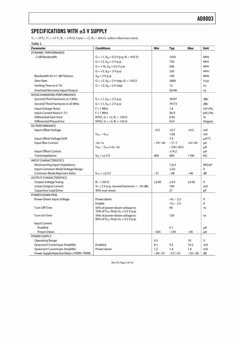
Figure 10. G = +1 Series Resistor (RS ) Optimization
0 5 7 2 1 - 0 0 9
1 100 1000 –7
–6
–5
–4
–3
–2
–1
0
1
2
3
FREQUENCY (MHz)
N O R M A L I Z E D
C L O S E D - L O O P G A I N
( d B )
10
VS = ±5VG = +1, RF = 432ΩG = +2, +5, RF = 464Ω
RL = 150ΩVOUT = 2V p-p
G = +1
G = +2
G = +5
Figure 11. Large Signal Frequency Response for Various Gains
G = +1RL = 100ΩVOUT = 2V p-p
0 5 7 2 1
- 0 1 7
–120
–110
–80
–70
–60
–90
–100
–50
–40
–30
0.1 1 10 100
FREQUENCY (MHz)
D I S T O R T I O N
( d B c )
THIRD
SECOND
VS = ±5VVS = +5V
Figure 12. Harmonic Distortion vs. Frequency for Various Supplies
G = +2RL = 150ΩVOUT = 2V p-p
0 5 7 2 1 - 0 1 6
–0.9
–0.8
–0.7
–0.6
–0.4
–0.2
–0.1
0.2
–0.5
–0.3
0.1
0
0.3
1 10 100 1000
FREQUENCY (MHz)
N O R M A L I Z E D
C L O S E
D - L O O P G A I N
( d B )
VS = ±5V
VS = +5V
Figure 13. 0.1 dB Flatness Response
0 5 7 2 1 - 0 1 0
1 100 1000 –7
–6
–5
–4
–3
–2
–1
0
1
2
3
FREQUENCY (MHz)
N O R M A L I Z E D
C L O S E D - L O O P G A I N
( d B )
10
VS = ±5VG = +2RL = 150Ω
VOUT = 2V p-p
T = +25°C
T = –40°C
T = +105°C
Figure 14. Large Signal Frequency Response for Various Temperatures
G = +2RL = 150ΩVOUT = 2V p-p
0 5 7 2 1
- 0 1 8
–120
–110
–80
–70
–60
–90
–100
–50
–40
–30
0.1 1 10 100
FREQUENCY (MHz)
D I S T O R T I O N
( d B c )
VS = ±5VVS = +5V
THIRD
SECOND
Figure 15. Harmonic Distortion vs. Frequency for Various Supplies
8/3/2019 AD8003 Triple 1
http://slidepdf.com/reader/full/ad8003-triple-1 8/16
AD8003
Rev. B | Page 8 of 16
G = +2VOUT = 2V p-p
f C = 5MHz
0 5 7 2 1 - 0 1 9
–90
–60
–50
–40
–70
–80
–30
–20
–10
10 12 14 16 18 20 22 24 26 28 30
RL (Ω)
D I S T O R T I O
N
( d B c )
VS = ±5VVS = +5V
THIRD
SECOND
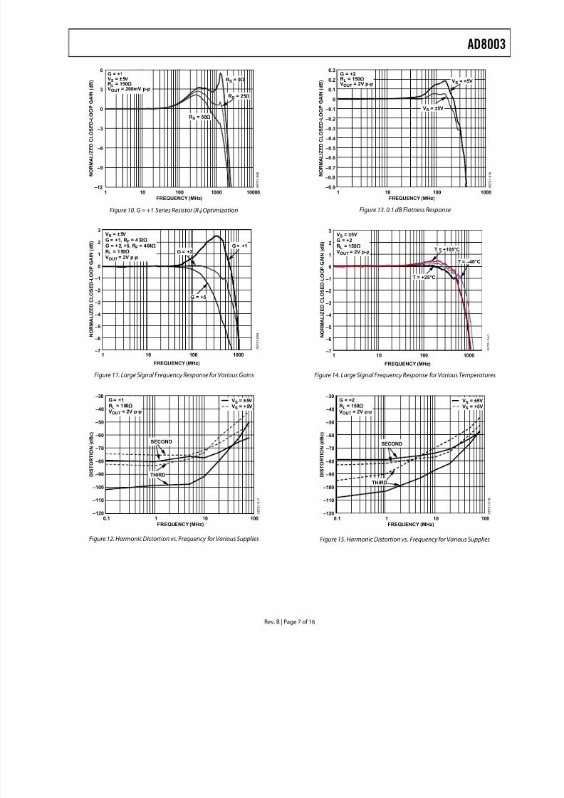
Figure 16. Harmonic Distortion vs. RL
G = +2RL = 150ΩVOUT = 2V p-p
0 5 7 2 1 - 0 1 2 –2.0
–1.5
1.5
–1.0
1.0
–0.5
0.5
0
2.0
0 15
TIME (ns)
O U T P U T V O L T A G E ( V )
VS = +5V
VS = ±5V
1 2 3 4 5 6 7 8 9 10 11 12 13 140.5
1.0
4.0
1.5
3.5
2.0
3.0
2.5
4.5
O U T P U T V O L T A G E ( V )
Figure 17. Large Signal Pulse Response for Various Supplies
G = +2RL = 150ΩVS = 5V
VOUT = 200mV p-p 0 5 7 2
1 - 0 2 2
2.2
2.5
2.6
2.7
2.4
2.3
2.8
0 5 10 15 20 25 30 35
TIME (ns)
O U T P U T V O L T A G E ( V )
CL = 0pF
CL = 15pF
CL = 27pF
Figure 18. Small Signal Pulse Response for Various Capacitive Loads
G = +2RL = 150ΩVOUT = 200mV p-p
0 5 7 2 1 - 0 1 1 –0.20
–0.15
0.15
–0.10
0.10
–0.05
0.05
0
0.20
0 1
TIME (ns)
O U T P U T V O L T A G E ( V )
2.30
2.35
2.65
2.40
2.60
2.45
2.55
2.50
2.70
O U T P U T V O L T A G E ( V )
5
VS = +5V
VS = ±5V
1 2 3 4 5 6 7 8 9 10 11 12 13 14
Figure 19. Small Signal Pulse Response for Various Supplies
G = +2RL = 150ΩVS = ±5VVOUT = 200mV p-p
0 5 7 2 1 - 0 2 0
–0.3
0
0.1
0.2
–0.1
–0.2
0.3
0 5 10 15 20 25 30 35
TIME (ns)
O U T P U T V O L T A G E ( V )
CL = 0pF
CL = 15pF
CL = 27pF
Figure 20. Small Signal Pulse Response for Various Capacitive Loads
0 5 7 2 1 - 0 2 1 –1.5
0
0.5
1.0
–0.5
–1.0
1.5
–5 0 105 15 20 25 30 35 40 45
TIME (ns)
A M P L I T U D E ( V )
–0.3
0
0.1
0.2
–0.1
–0.2
0.3
S E T T L I N G ( % )
VIN
VSETTLE
VOUTG = +2VS = ±5VRL = 150Ω
Figure 21. Short-Term 0.1% Settling Time

8/3/2019 AD8003 Triple 1
http://slidepdf.com/reader/full/ad8003-triple-1 9/16
AD8003
Rev. B | Page 9 of 16
G = +2RL = 150Ω
0 5 7 2 1 - 0 1 3
0
5000
4000
1000
3000
2000
6000
0 7
VOUT p-p (V)
S L E W R
A T E ( V / µ s )
VS = +5V
VS = ±5V
1 2 3 4 5 6
RISEFALL
Figure 22. Slew Rate vs. Output Voltage
G = +2VS = ±5VR
L= 150Ω
0 5 7 2 1 - 0 2 4
–5
–4
–3
–2
–1
0
1
2
3
4
5
0 0.1 0.2 0.3 0.4 0.5 0.6 0.7 0.8 0.9 1.0
TIME (µs)
A M P L I T U D E ( V )
OUTPUT
INPUT × 2
Figure 23. Output Overdrive Recovery
G = 0VS = ±5VRL = 150Ω
0 5 7 2 1
- 0 2 6
–60
–40
–50
–30
–10
–20
0
0.1 1 10 100
FREQUENCY (MHz)
C O M M O N - M O D E R E J E C T I O N ( d B )
Figure 24. Common-Mode Rejection vs. Frequency
G = +1VS = ±5VRL = 150Ω
0 5 7 2 1 - 0 2 3
–5
–4
–3
–2
–1
0
1
2
3
4
5
0 0.1 0.2 0.3 0.4 0.5 0.6 0.7 0.8 0.9 1.0
TIME (µs)
A M P L I T U
D E ( V )
OUTPUT
INPUT
Figure 25. Input Overdrive Recovery
G = +1/+2VS = ±5V
0 5 7 2 1 - 0 2 7
0.1
1
100
10
1000
0.1 1 10 100 1000
FREQUENCY (MHz)
I M P E D A N C E ( Ω )
Figure 26. Output Impedance vs. Frequency
G = +2VS = ±5VRL = 150Ω
0 5 7 2 1
- 0 2 5
–70
–60
–40
–50
–30
–10
–20
0
0.1 1 10 100 1000
FREQUENCY (MHz)
P O W E R S U P P L Y R E J E C T I O N ( d B )
PSR–
PSR+
Figure 27. Power Supply Rejection vs. Frequency

8/3/2019 AD8003 Triple 1
http://slidepdf.com/reader/full/ad8003-triple-1 10/16
AD8003
Rev. B | Page 10 of 16
0 5 7 2 1 - 0 3 1
–5 –4 –3 –2 –1 0 1 2 3 4 –60
–40
–20
0
20
60
80
5
VCM (V)
V O S ( m
V )
40
VS = ±5VVS = +5V
Figure 28. Offset Voltage vs. Input Common-Mode Range
0 5 7 2 1 - 0 3 3
–5 –4 –3 –2 –1 0 1 2 3 4 –10
–8
–6
–4
–2
0
2
4
6
8
10
5
VOUT (V)
I B ( μ A )
VS = ±5V
VS = +5V
Figure 29. Inverting Input Bias Current Linearity
G = +2RL = 150ΩVS = ±5V
0 5 7 2 1 - 0 2 80
1
9
8
7
2
6
3
5
4
10
–5 5
POWER DOWN PIN VOLTAGE (VDIS (V))
P O S I T I V E S U P P L Y C U R R E N T ( m A )
–300
–250
150
–200
100
–50
–100
–150
50
0
200
P O W E R D O W N P I N C U R R E N T ( µ A )
IDIS
ICC
–4 –3 –2 –1 0 1 2 3 4
Figure 30. POWER DOWN Pin Current and Supply Current vs.POWER DOWN Pin Voltage
0 5 7 2 1 - 0 3 2
–5 –4 –3 –2 –1 0 1 2 3 4 –20
–15
–10
–5
0
5
15
20
5
VCM (V)
I B ( µ A
)
10 VS = ±5V VS = +5V
Figure 31. Noninverting Input Bias Current vs. Common-Mode Range
G = +2RL = 150ΩVIN = 0.5V dc
0 5 7 2 1 - 0 1 4
0
5
4
1
3
2
6
0 1
TIME (µs)
A M P L I T U D E ( V )
.0
VDIS (VS = ±5V)
VOUT (VS = ±5V)
VOUT (VS = ±5V)
VOUT (VS = +5V)
0.1 0.2 0.3 0.4 0.5 0.6 0.7 0.8 0.9
VDIS (VS = +5V)
VOUT (VS = +5V)
Figure 32. Disable Switching Time for Various Supplies
G = +2RL = 150ΩVS = 5V
0 5 7 2 1 - 0 2 90
1
9
8
7
2
6
3
5
4
10
0 5
POWER DOWN PIN VOLTAGE (VDIS (V))
P O S I T I V E S U P P L Y C U R R E N T ( m A )
–60
–50
30
–40
20
–10
–20
–30
10
0
40
P O W E R D O W N P I N C U R R E N T ( µ A )
.0
IDISICC
0.5 1.0 1.5 2.0 2.5 3.0 3.5 4.0 4.5
Figure 33. POWER DOWN Pin Current and Supply Current vs.POWER DOWN Pin Voltage

8/3/2019 AD8003 Triple 1
http://slidepdf.com/reader/full/ad8003-triple-1 11/16
AD8003
Rev. B | Page 11 of 16
0 5 7 2 1 - 0 3 4
10 100 1k 10k 100k 1M 10M1
10
100
1000
FREQUENCY(Hz)
I N P U T V O L T A G E N
O I S E ( n V / √ H z )
VS = ±5VRF = 1kΩ
Figure 34. Input Voltage Noise vs. Frequency
G = +2RL = 150Ω
DRIVING: CH1 AND CH3RECEIVING: CH2
0 5 7 2 1 - 0 1 5
–100
–50
–60
–70
–80
–90
–40
–30
–20
–10
0
0.1 1 10 100 1000
FREQUENCY (MHz)
N O R M A L I Z E D C L O S E D - L O O P G A I N ( d B
) VS = ±5V
VS = +5V
Figure 35. Worst-Case Crosstalk
0 5 7 2 1 - 0 3 5
10 100 1k 10k 100k 1M 10M1
100
1000
10000
FREQUENCY (Hz)
10
I N P U T C U R R E N T N
O I S E ( p A / √ H z )
VS = ±5V
I–
I+
Figure 36. Input Current Noise vs. Frequency
0 5 7 2 1 - 0 3 0
1k 10k 100k 1M 10M 100M 1G
100
1k
10k
100k
1M
FREQUENCY (Hz)
M A G N I T U D E ( Ω )
P H A S E ( D e g r e e s )
0
20
40
60
80
120
140
160
180
200
100
Figure 37. Transimpedance

8/3/2019 AD8003 Triple 1
http://slidepdf.com/reader/full/ad8003-triple-1 12/16
AD8003
Rev. B | Page 12 of 16
APPLICATIONS INFORMATIONGAIN CONFIGURATIONS
Unlike conventional voltage feedback amplifiers, the feedbackresistor has a direct impact on the closed-loop bandwidth and
stability of the current feedback op amp circuit. Reducing theresistance below the recommended value can make the amplifierresponse peak and can even become unstable. Increasing thesize of the feedback resistor reduces the closed-loop bandwidth.
Table 5 provides a convenient reference for quickly determiningthe feedback and gain set resistor values, and the small andlarge signal bandwidths for common gain configurations. Thefeedback resistors in Table 5 have been optimized for 0.1 dBflatness frequency response.
Table 5. Recommended Values and Frequency Response1
Gain RF (Ω) RG (Ω) RS (Ω)
−3 dB
SS BW(MHz)
LargeSignal
−3 dBBW
LargeSignal
0.1 dBBW
−1 300 300 0 734 668 --+1 432 N/A 24.9 1650 822 --
+2 464 464 0 761 730 190
+5 300 75 0 567 558 165
+10 300 33.2 0 446 422 1701Conditions: VS = ±5 V, TA = 25°C, RL = 150 Ω.
Figure 38 and Figure 39 show the typical noninverting and invertingconfigurations and recommended bypass capacitor values.
FB
AD8003
10µF
0.1µF
RG
RS
+VS
VO
VIN RL
–
+VO
+V
–VS
–V
10µF
0.1µF
RF
0 5 7 2 1 - 0 3 8
Figure 38. Noninverting Gain
FB
AD8003
10µF
0.1µF
RG
+VS
VO
VIN
RL
–
+VO
+V
–VS
–V
10µF
0.1µF
RF
0 5 7 2 1 - 0 3 9
Figure 39. Inverting Gain
RGB VIDEO DRIVER
Figure 40 shows a typical RGB driver application using bipolarsupplies. The gain of the amplifier is set at +2, where RF = RG =
464 Ω. The amplifier inputs are terminated with shunt 75 Ωresistors, and the outputs have series 75 Ω resistors for proper video matching. In Figure 40, the POWER DOWN pins are notshown connected to any signal source for simplicity. If the power-down function is not used, it is recommended that the POWERDOWN pins be tied to the positive supply and not be left floating(not connected).
In applications that require a fixed gain of +2, as previously mentioned, the designer may consider the ADA4862-3.The ADA4862-3 is another high performance triple currentfeedback amplifier. The ADA4862-3 has integrated feedbackand gain set resistors that reduce board area and simplify designs.
+VS
10µF
0.1µF
–VS
10µF
0.1µF
+VS
10µF
0.1µF
–VS
10µF
0.1µF
75Ω
75Ω
GIN
0 5 7 2 1 - 0 3 6
21
22
19
2 4
RF464Ω
75ΩRG
464Ω
75Ω
RIN
PD1
3
2
4
PD2
PD3
1
+VS
10µF
0.1µF
75Ω
75Ω
BIN
GOU
14235
T
ROUT
BOUT
–VS
10µF
0.1µF
6
16
17
15
18
13
RF464Ω
RG
464Ω
20
RF
464Ω
RG
464Ω
AD8003
Figure 40. RGB Video Driver

8/3/2019 AD8003 Triple 1
http://slidepdf.com/reader/full/ad8003-triple-1 13/16
AD8003
Rev. B | Page 13 of 16
PRINTED CIRCUIT BOARD LAYOUTPrinted circuit board (PCB) layout is usually one of the laststeps in the design process and often proves to be one of themost critical. A high performance design can be renderedmediocre due to poor or sloppy layout. Because the AD8003can operate into the RF frequency spectrum, high frequency board layout considerations must be taken into account. ThePCB layout, signal routing, power supply bypassing, andgrounding must all be addressed to ensure optimal performance.
LOW DISTORTION PINOUT
The AD8003 LFCSP features ADI’s low distortion pinout. Thepinout lowers the second harmonic distortion and simplifies thecircuit layout. The close proximity of the noninverting inputand the negative supply pin creates a source of second harmonicdistortion. Physical separation of the noninverting input pinand the negative power supply pin reduces this distortion.
By providing an additional output pin, the feedback resistorcan be connected directly between the feedback pin and theinverting input. This greatly simplifies the routing of thefeedback resistor and allows a more compact circuit layout,which reduces its size and helps to minimize parasitics andincrease stability.
SIGNAL ROUTING
To minimize parasitic inductances, ground planes should beused under high frequency signal traces. However, the groundplane should be removed from under the input and output pinsto minimize the formation of parasitic capacitors, which degrades
phase margin. Signals that are susceptible to noise pickup should berun on the internal layers of the PCB, which can providemaximum shielding.
EXPOSED PADDLE
The AD8003 features an exposed paddle, which lowers thethermal resistance by approximately 40% compared to astandard SOIC plastic package. The paddle can be soldereddirectly to the ground plane of the board. Thermal vias or heatpipes can also be incorporated into the design of the mountingpad for the exposed paddle. These additional vias improve thethermal transfer from the package to the PCB. Using a heavierweight copper also reduces the overall thermal resistance path
to ground.
POWER SUPPLY BYPASSING
Power supply bypassing is a critical aspect of the PCB designprocess. For best performance, the AD8003 power supply pins
need to be properly bypassed.Each amplifier has its own supply pins brought out for the utmostflexibility. Supply pins can be commoned together or routed to adedicated power plane. Commoned supply connections can alsoreduce the need for bypass capacitors on each supply line. Theexact number and values of the bypass capacitors are dictatedby the design specifications of the actual circuit.
A parallel combination of different value capacitors from eachof the power supply pins to ground tends to work the best.Paralleling different values and sizes of capacitors helps to ensurethat the power supply pins see a low ac impedance across a wideband of frequencies. This is important for minimizing the couplingof noise into the amplifier. Starting directly at the power supply pins, the smallest value and physical-sized component shouldbe placed on the same side of the board as the amplifier, and asclose as possible to the amplifier, and connected to the groundplane. This process should be repeated for the next largest capacitor
value. It is recommended that a 0.1 μF ceramic 0508 case be usedfor the AD8003. The 0508 offers low series inductance andexcellent high frequency performance. The 0.1 μF case provideslow impedance at high frequencies. A 10 μF electrolytic capacitorshould be placed in parallel with the 0.1 μF. The 10 μF capacitorprovides low ac impedance at low frequencies. Smaller valuesof electrolytic capacitors can be used depending on the circuit
requirements. Additional smaller value capacitors help provide alow impedance path for unwanted noise out to higherfrequencies but are not always necessary.
Placement of the capacitor returns (grounds), where the capacitorsenter into the ground plane, is also important. Returning thecapacitor grounds close to the amplifier load is critical fordistortion performance. Keeping the capacitors distance short,but equal from the load, is optimal for performance.
In some cases, bypassing between the two supplies can helpimprove PSRR and maintain distortion performance incrowded or difficult layouts. Designers should note this asanother option for improving performance.

8/3/2019 AD8003 Triple 1
http://slidepdf.com/reader/full/ad8003-triple-1 14/16
AD8003
Rev. B | Page 14 of 16
Minimizing the trace length and widening the trace from thecapacitors to the amplifier reduces the trace inductance. Aseries inductance with the parallel capacitance can form a tankcircuit, which can introduce high frequency ringing at the output.This additional inductance can also contribute to increased
distortion due to high frequency compression at the output.The use of vias should be minimized in the direct path to theamplifier power supply pins because vias can introduce parasiticinductance, which can lead to instability. When required, usemultiple large diameter vias because this lowers the equivalentparasitic inductance.
GROUNDING
The use of ground and power planes is encouraged as a methodof proving low impedance returns for power supply and signalcurrents. Ground and power planes can also help to reduce stray trace inductance and provide a low thermal path for the amplifier.
Ground and power planes should not be used under any of thepins of the AD8003. The mounting pads and the ground or powerplanes can form a parasitic capacitance at the amplifiers input.Stray capacitance on the inverting input and the feedbackresistor form a pole, which degrades the phase margin, leadingto instability. Excessive stray capacitance on the output also forms apole, which degrades phase margin.

8/3/2019 AD8003 Triple 1
http://slidepdf.com/reader/full/ad8003-triple-1 15/16
AD8003
Rev. B | Page 15 of 16
OUTLINE DIMENSIONS
124
67
13
1918
12
2.25
2.10 SQ
1.95
0.60 MAX
0.50
0.40
0.30
0.30
0.23
0.18
2.50 REF
0.50BSC
12° MAX0.80 MAX
0.65TYP0.05 MAX
0.02 NOM
1.00
0.85
0.80
SEATINGPLANE
PIN 1INDICATOR TOP
VIEW3.75
BSC SQ
4.00BSC SQ
PIN 1INDICATOR
0.60 MAX
COPLANARITY0.080.20 REF
0.25 MIN
EXPOSEDPAD
(BOTTOM VIEW)
COMPLIANT TOJEDEC STANDARDS MO-220-VGGD-2
Figure 41. 24-Lead Lead Frame Chip Scale Package [LFCSP_VQ]4 mm × 4 mm Body, Very Thin Quad
(CP-24-1)Dimensions shown in millimeters
ORDERING GUIDEModel Temperature Range Package Description Package Option Ordering Quantity
AD8003ACPZ-R2 1 –40°C to +85°C 24-Lead LFCSP_VQ CP-24-1 250
AD8003ACPZ-REEL1 –40°C to +85°C 24-Lead LFCSP_VQ CP-24-1 5,000
AD8003ACPZ-REEL7 1 –40°C to +85°C 24-Lead LFCSP_VQ CP-24-1 1,500
EVAL-AD8003-3CPEZ 1 Evaluation Board
1 Z = RoHS Compliant Part.

8/3/2019 AD8003 Triple 1
http://slidepdf.com/reader/full/ad8003-triple-1 16/16
AD8003
Rev. B | Page 16 of 16
NOTES
©2005–2008 Analog Devices, Inc. All rights reserved. Trademarks andregistered trademarks are the property of their respective owners.
D05721-0-9/08(B)