ac boundary-scan - ieeegrouper.ieee.org/groups/1149/6/doc/ieee_acjtag.pdfac boundary-scan ©...
TRANSCRIPT

1© 2001,C i sco Syst em s,Inc.AC Boundary-Scan
AC BoundaryAC Boundary --ScanScanCisco Systems, IncCisco Systems, Inc

2© 2001,C i sco Syst em s,Inc.AC Boundary-Scan
AC BoundaryAC Boundary --Scan:Scan:BoundaryBoundary --scan beyond DCscan beyond DC
ASIC DFT GroupASIC DFT Group
Sung Chung and SangSung Chung and Sang BaegBaegMay 21, 2001May 21, 2001
2AC Boundary-Scan © 1999,C i sco Syst em s,Inc.Conf ident ial

5AC Boundary-Scan © 2001,C i sco Syst em s,Inc. www .acext est .org
Problem StatementProblem Statement
• AC Coupled net between high speed devices
Conventional JTAG does not work
No JTAG infrastructure to test AC coupled net
• Many Optics / SERDES use “AC Coupling”
• Interoperability demands more “AC Coupling”between high speed devices
• Differential line lacks 1149.1 Test Coverage

6AC Boundary-Scan © 2001,C i sco Syst em s,Inc. www .acext est .org
Current StatusCurrent Status
Device 1 Device 2 orConnector
STD 1149.1incapable
STD 1149.1capable
STD 1149.1incapable
EXTEST
AC_EXTEST
AC_EXTEST

7AC Boundary-Scan © 2001,C i sco Syst em s,Inc. www .acext est .org
AC BoundaryAC Boundary --Scan OverviewScan Overview
• AC Pattern Generation at scan cell
• AC Pattern Application & Sample at RTI
• AC Pattern Capture at scan cell
• Maintains DC boundary-scan compatibility
• DC & AC Operate at different TAP state

8AC Boundary-Scan © 2001,C i sco Syst em s,Inc. www .acext est .org
AC BoundaryAC Boundary --Scan OperationScan Operation
• Setup EXTEST value: logic 1 or 0
• Execute AC_EXTEST command
• AC pattern is applied @ RTI
• Internal Sync Pulse samples a logicstate from incoming AC pattern
• Capture_DR captures a sampled value
• Shift_DR for test evaluation

9AC Boundary-Scan © 2001,C i sco Syst em s,Inc. www .acext est .org
Problem Transmission LinesProblem Transmission Lines
Data InLogic 1 or 0
Data OutLogic 1 or 0
VOUTVIN
VCM
VGND
Common Ground Return
Signal Line
Driver Receiver
Logic 1 or 0
Data InLogic 1 or 0
Data OutLogic 1 or 0
VOUT
VDiff
VCM
VGND
Common Ground Return
Signal LinePositive
Diff.Driver
Diff.Receiver
Logic 1 or 0VCM
Signal LineNegative
Logic 1 or 0
2 LogicState
4 LogicState
2 LogicState
FaultMask

10AC Boundary-Scan © 2001,C i sco Syst em s,Inc. www .acext est .org
Fault Model for Spice SimulationFault Model for Spice Simulation
TargetDriver
TargetReceiver
Fault injection optionR = 0 Ω Ω Ω Ω : Shorted netR = ∝ Ω ∝ Ω ∝ Ω ∝ Ω : Opened net
Transmission line optionR = 0 Ω Ω Ω Ω : DC netR = ∝ Ω ∝ Ω ∝ Ω ∝ Ω : AC net

11AC Boundary-Scan © 2001,C i sco Syst em s,Inc. www .acext est .org
Expanded Fault Model 1Expanded Fault Model 1
ReferenceDriver 1
TargetDriver
ReferenceDriver 2
3'
2
4
5'
3
1
5
2'
4'
1'
A
B
ReferenceReceiver 1
ReferenceReceiver 2
TargetReceiver

12AC Boundary-Scan © 2001,C i sco Syst em s,Inc. www .acext est .org
Expanded Fault Model 2Expanded Fault Model 2
A
B
Vref TargetReceiver
3'
5'
2'
4'
2
4
3
1
5
1'

13AC Boundary-Scan © 2001,C i sco Syst em s,Inc. www .acext est .org
Test Buffer and Fault ClassesTest Buffer and Fault Classes
AC Status Detection
TerminationNetwork
Highspeed signal path
Null Detection
Short Detection
Test Buffer

14AC Boundary-Scan © 2001,C i sco Syst em s,Inc. www .acext est .org
Fault Detection and Error StatusFault Detection and Error Status
Fault detection criteriaResulting Error StatusNull or Float
StatusShortStatus
ACStatus
0 0 0
No float, no short, no AC status.Coupling component open or noise below common mode voltage,technology dependent behavior but result in error condition.No Error Condition for DC mode
0 0 1No float, no short, AC status.No Error Condition, normal operation in AC mode
0 1 0No float, short, no AC status.Both A and B short, or shorted with power or ground rail
0 1 1No null, short, AC status.A and B short.
1 0 0Null or float with no short, no AC status.A and B open, no short between A and B.
1 0 1Null or float with no short, AC status.A or B open.
1 1 0Null or float, short, no AC status.A and B open at driver, or short at receiver, technology dependentbehavior but result in error.
1 1 1Null or float, short, AC status.Condition is not feasible by structural fault.

15AC Boundary-Scan © 2001,C i sco Syst em s,Inc. www .acext est .org
Why Fault ClassesWhy Fault Classes
• Fault Model changes constantly.. as Technology changes.. as Defects changes.. as board topology and usage changesThere will be never enough Fault Models
• Identify un-defined logic state with Null sensor“00” or “11” logic state in differential line
Don’t let functional logic makes decision for Test, it ismade to tolerate such conditions during functional mode
• Null / Short / AC Status need to be identified withinfunctional domain of the device
• Test Buffer must evolve as technology evolvesNew technology invents new faults

16AC Boundary-Scan © 2001,C i sco Syst em s,Inc. www .acext est .org
Special SignalsSpecial Signals
Clk
D
Q
QS
AC_Test_Marker
AC_Pattern-Source
AC_Pattern_Clock
Clk
D
Q
QS
AC_Test_Marker
AC_Test_Ran
UpdateDRR
Reset
Logic Low
Clk
D
Q
Q
Clk
D Q
AC_Test
AC_Pattern_Clock AC_Test_Marker
Clk
D Q
TCK =AC Pattern Clock
AC_Test
AC_Test_Marker
A
B
C
AC Pattern
AB
C

17AC Boundary-Scan © 2001,C i sco Syst em s,Inc. www .acext est .org
Timing DiagramsTiming Diagrams
TCK =AC Pattern
Clock
AC Pattern
Run-Test/IdleTAP State
AC_Sync
AC Pattern Clock Cycle
AC Pattern Cycle
Run/Test Idle Duration
AC Pattern Sample Interval = Every 16 th AC Pattern Cycle
1st AC Pattern Cycle 16th AC Pattern Cycle
Next AC PatternSample Interval
AC_Sync
TCK
AC Pattern = 1
Run-Test / Idle
AC Pattern = 0
18AC Boundary-Scan © 2001,C i sco Syst em s,Inc. www .acext est .org
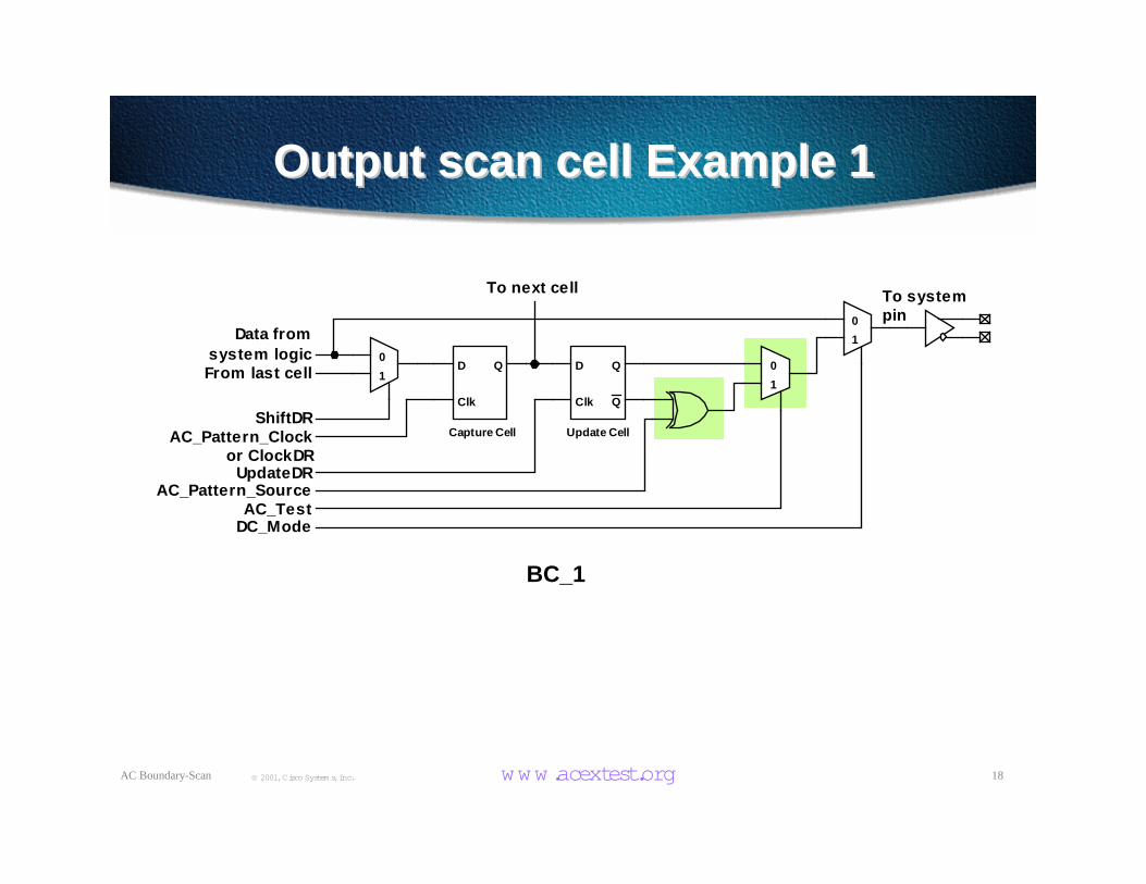
Output scan cell Example 1Output scan cell Example 1
1
0
1
0
Clk
D
Q
Q
Data fromsystem logic
From last cell
ShiftDR
UpdateDR
AC_TestDC_Mode
To next cell To systempin
Clk
D Q1
0
AC_Pattern_Source
Capture Cell Update CellAC_Pattern_Clockor ClockDR
BC_1

19AC Boundary-Scan © 2001,C i sco Syst em s,Inc. www .acext est .org
Output scan cell Example 2Output scan cell Example 2
1
0
1
0
Clk
D
Q
Q
Clk
D
Q
Q1
01
0S
AC_Test_Marker
Data fromsystem logic
From last cell
ShiftDR
AC_Test
UpdateDRAC_Test
DC_Mode
To next cellTo systempin
AC_Pattern_Clockor ClockDR
BC_1

20AC Boundary-Scan © 2001,C i sco Syst em s,Inc. www .acext est .org
Output scan cell Example 3Output scan cell Example 3
AC_Pattern_Clockor ClockDR
1
0
1
0
Clk
D
Q
Q1
01
0
Data fromsystem logic
From last cell
ShiftDR
UpdateDR
AC_Test
DC_Mode
To next cell To systempin
10
Clk
D Q
AC_Test_Marker
AC_Test
BC_1

21AC Boundary-Scan © 2001,C i sco Syst em s,Inc. www .acext est .org
Input scan cell Example 1Input scan cell Example 1
Clk
D Q 1
0
1
0
1
0
Clk
D Q
Clk
D Q
AC_Test_Ran
Data tosystemlogic
From last cell
To next cellFrom
systempin
AC_Sync
DC_ModeUpdateDR
ClockDRShiftDR
Capture Cell Update CellAC PatternHold Cell
BC_1

22AC Boundary-Scan © 2001,C i sco Syst em s,Inc. www .acext est .org
Input scan cell Example 2Input scan cell Example 2
Clk
D Q 1
0
1
0
Clk
D Q
AC_Test_Ran
Data tosystemlogic
From last cell
To next cellFrom
systempin
AC_Sync
ClockDRShiftDR
BC_4

23AC Boundary-Scan © 2001,C i sco Syst em s,Inc. www .acext est .org
AC_EXTEST control cell ExampleAC_EXTEST control cell Example
1
0
1
0
Clk
D
Q
QOutput Data
ShiftDR
UpdateDR
AC_Test
Mode
Tosystem
pin
1
0
AC_Pattern_Source
BC_1Output Cell
BC_1
ClockDR
UpdateDR
To next cell
Clk
D Q
Clk
D Q
AC_EXTEST Control Cell
From last cell
Clk
D Q
AC_Pattern_Clock or ClockDR

24AC Boundary-Scan © 2001,C i sco Syst em s,Inc. www .acext est .org
BidiBidi scan cell Example 1scan cell Example 1
BC_1
Clk
D Q 1
0
1
0
Clk
D Q
AC_Test_Ran
Input Data
From last cell
AC_Sync
ClockDRShiftDR
ClockDR
1
0
1
0
Clk
D
Q
QOutput Data
ShiftDR
UpdateDR
AC_TestMode
To systempin
Clk
D Q1
0
AC_Pattern_Source
ClockDR
1
0
Output Control
ShiftDR
UpdateDR
To next cell
Clk
D Q1
0
Clk
D Q
Mode
BC_1
BC_4
Output Cell
Control Cell
Input Cell

25AC Boundary-Scan © 2001,C i sco Syst em s,Inc. www .acext est .org
BidiBidi scan cell Example 2scan cell Example 2
Clk
D Q
1
0
1
0
Clk
D Q
1
0
Clk
D
Q
Q
Clk
D Q
1
0
1
0
Bidirectional Cell BC_7
BC_2Control Cell
Output Data
ClockDR
Output Control
Mode_1
AC_Sync
From last cellShiftDR
UpdateDR
Input Data
AC_Pattern_SourceAC_Test
1
0
ShiftDR
AC_Test_Ran
ClockDRUpdateDR
To systempin
To next cell Mode_3
1
0
Clk
D Q
Mode_2
10

26AC Boundary-Scan © 2001,C i sco Syst em s,Inc. www .acext est .org
BidiBidi scan cell Example 3scan cell Example 3
Clk
D Q
1
0
1
0Clk
D Q
1
0
Clk
D
Q
Q
Clk
D Q
1
0
1
0
Bidirectional Cell BC_8
BC_2Control Cell
Output Data
ClockDR
Output Control
Mode
AC_Sync
From last cellShiftDR
UpdateDR
Input Data
AC_Pattern_SourceAC_Test
Clk
D Q 1
0
ShiftDR
AC_Test_Ran
ClockDRUpdateDR
To systempin
To next cell

27AC Boundary-Scan © 2001,C i sco Syst em s,Inc. www .acext est .org
AC_EXTEST: Superset of EXTESTAC_EXTEST: Superset of EXTEST
This table shows effect of eachinstruction within the device which hasboth AC and DC boundary-scan cells
EXTESTEXTESTEXTESTEXTEST
EXTESTEXTESTAC_EXTESTAC_EXTEST
Bypassing RTIPassing through RTIDC scan cell
AC scan cell
Execution effects after Capture-DR
Instruction

28AC Boundary-Scan © 2001,C i sco Syst em s,Inc. www .acext est .org
Compatibility mode between devicesCompatibility mode between devices
Receiving AC Scan Cell ( through DC net )
Passing through RTI Bypassing RTI
EXTEST AC_EXTEST EXTEST AC_EXTEST
DrivingAC
ScanCell
EXTEST Capture DC 1 Capture DC 2 Capture DC 1,3 Capture DC 2,3
AC_EXTEST Unknown 4 Capture AC Capture DC 3 Capture DC 3
NOTE1. Backward compatibility: interoperable with DC scan cell with EXTEST
2. The AC_EXTEST is a superset of existing DC EXTEST capture operation.3. Input cell can capture DC under the AC_EXTEST.
4. Input cell captures unknown value.
Receiving AC Scan Cell ( through AC coupled net )
Passing through RTI Bypassing RTI
EXTEST AC_EXTEST EXTEST AC_EXTEST
DrivingAC
ScanCell
EXTEST Unknown 1,2 Unknown 1,2 Unknown 1,2 Unknown 1,2
AC_EXTEST Unknown 1 Capture AC Unknown 1,2 Unknown 1,2
NOTE1. All DC operations will capture unknown value due to AC coupling.
2. Presence of certain fault, sampling line status in DC may serve diagnostic purpose.

29AC Boundary-Scan © 2001,C i sco Syst em s,Inc. www .acext est .org
Jitter BudgetJitter Budget
6.25 nS40 MHz
12.5 nS20 MHz
25 nS10 MHz
50 nS5 MHz
Maximum JitterTCK Frequency
Lead 1/4 Cycle
Lag 1/4 Cycle
In phase
ReferenceSignal
Device 1
Device 2
Max Jitter = (1/4 Tck Cycle ) - (Setup or Hold time)
TCK = AC Pattern Clock
AC Pattern
AC_Sync

30AC Boundary-Scan © 2001,C i sco Syst em s,Inc. www .acext est .org
Scalability: Test Buffer vs. FrequencyScalability: Test Buffer vs. Frequency
Scalable by Test Pattern Frequency as technology changes orTest Buffer Approach based on technology used in design
Common Ground Return
Driver HighspeedData Path
Test Buffer
0.01µµµµF to 10pF
1 2
3
TCK
ScanCell
1
2with 0.01 µµµµF
2with 10pF
3
20 GHz
10 GHz ?4700pF to
10pF ?
5 GHz
2.5 GHz
?
10MHz to
20MHz
0.01µµµµF to
4700pF ?
1.25 GHz
CriticalFrequency
AC PatternRate
CouplingCap
ChannelData Rate

31AC Boundary-Scan © 2001,C i sco Syst em s,Inc. www .acext est .org
Coupling CapacitorCoupling Capacitor
• Practical issues with smaller coupling capacitorReactance and Inductance
Low loss Dielectric and low Parasitic
Impedance Magnitude at high speed
I/O characterization test makes on chip capacitors almost impossible
Capacitor may end up more easily on package substrate
Low capacitance value will increase low frequency Pattern-Dependent Jitter (PDJ) beyond functional tolerance
For a 2.488Gbps receiver, bit period Tb = 402 pS. If Maximum tolerated consecutiveidentical digits Ncid = 72 bits and termination resistor R=100 ΩΩΩΩ, calculated C is 2.25 nF.If rise time Tr = 120 pS and C = 2.25 nF, the calculated PDJ is 12 pS. If we increase C to
100 nF, the resulting PDJ will be reduced to less than 1 pS.Choosing AC Coupling Capacitors from Maxim http://pdfserv.maxim-ic.com/arpdf/AppNotes/hfan11v2.pdf
Does capacitor value ever decrease as frequency increases??

32AC Boundary-Scan © 2001,C i sco Syst em s,Inc. www .acext est .org
BSDL SupportBSDL Support
• AC_EXTEST is currently contained within the Extension
BSDL does not disturb existing tools
One BSDL serve both DC and AC
• Multiple AC_EXTEST Instruction & Execution support
• Selective AC_EXTEST disable function
• Easy to create:
Register list identifies AC_EXTEST capable cells
Duplicate from existing DC register list
• Parser will be ready within a month

33AC Boundary-Scan © 2001,C i sco Syst em s,Inc. www .acext est .org
Why Cisco MSA Approach??Why Cisco MSA Approach??
• KISS (Keep It Simple and Smart)Simple, minimum overhead, and self-containedNo extra test pinVery little effort from DC boundary-scan designAutonomous and transparent to ATE and CAE tools
• CompatibilityBackward compatible and coexist with legacy DC boundary-scan device in DC modeRuns either DC, AC, or both during testNo investment loss: if it was working, it will be working
• High Noise immunityOperate AC and DC in separate TAP stateNo AC interference during DC test: preserve DC test coverageDifferential input Test Buffer filters tester related CM noise
• ScalabilityNo need to scale with functional speed and technology change

34AC Boundary-Scan © 2001,C i sco Syst em s,Inc. www .acext est .org
Brief Development HistoryBrief Development History
• Initial study completedMay 1st, ‘00: Draft completed
• AC_EXTEST Specification ReleaseJune 8th, ‘00: Cisco internal releaseJune 8th to June 12th ‘00: Release to all MSA partners
• Follow on researchOct ’00: RTL verification completedNov ’00: selected fault Spice simulation completedPatent filed
• Demo Board and RTL Verification toolDemo Board is in PCB routing and signal IntegrityParser is in debug
• Supporting 2 internal projects5 or more MSA partners to meet test need for the project within next 18month