a laser scanner chip set for accurate perception systems · a laser scanner chip set for accurate...
TRANSCRIPT
313A Laser Scanner Chip Set for Accurate Perception Systems 313
A Laser Scanner Chip Set for Accurate Perception Systems
S. Kurtti, J.-P. Jansson, J. Kostamovaara, University of Oulu
Abstract
This paper presents an integrated receiver channel and an inte-grated time-to-digital (TDC) converter fabricated in a 0.35 mm SiGe BiCMOS and in 0.35 mm CMOS technologies, respectively, that give the required performance for a pulsed time-of-flight (TOF) laser radar to be used in a laser scanner in automotive applications. The receiver-TDC chip set is capable to measure the positions and widths of three separate successive timing pulses with sub-ns level precision in a wide dynamic amplitude range of more than 1:10.000.
1 Introduction
The pulsed time-of-flight (TOF) laser distance measurement method is based on the measurement of the transit time of a short laser pulse to an optically visible target and back to the receiver, Figure 1. This method offers several advan-tages in terms of high measurement speed (<ms), high lateral and longitudal accuracy (mm-cm) and dynamic range and is thus considered to be a potential solution for perception systems in traffic and in robot vision, for example. Due to practical reasons the laser pulse length used is typically in the range of 3-5ns. This corresponds to 1-2 meters in air. On the other hand in practical applications an accuracy of a few centimeters is typically called for. Then, obvi-ously, a stable pulse shape and the detection of a specific point of the received laser pulse are needed. This is alleviated by the fact that the amplitude of the received laser echo may vary in a range of 1:10.000 or even more.
In this work we have developed two integrated circuits which realize the functionalities of a pulsed time-of-flight laser scanner receiver. The receiver chip produces from the weak optical echo a digital timing pulse for the time-to-digital converter, whereas the TDC measures the time interval between the transmitted and received pulses. The receiver-TDC circuits can in fact meas-ure simultaneously the time intervals to three successive pulses and also the widths of the detected pulses. The width information can be used to correct the timing walk error as is presented in more details below.

Components & Systems314
Fig. 1. Block diagram of the pulse TOF rangefinder
2 Receiver Channel
A simplified block diagram of the receiver channel is shown in Fig. 2 a). The optical echo is converted to a current pulse in an external avalanche photodi-ode (APD). The current pulse is converted to a voltage pulse in a trans-imped-ance pre-amplifier and then further amplified in a voltage-type post amplifier. A constant threshold voltage is used at the input of the timing comparator generating a logic-level timing signals for the multi-channel TDC. The TDC measures the start (generated by laser transmitter) - stop (echo or possibly multiple echoes from the target) delays and the timing pulse lengths. In addi-tion the receiver chip includes needed bias blocks.
Fig. 2. Block diagram of the receiver channel (left), Photograph of the IC receiver channel (right)

315A Laser Scanner Chip Set for Accurate Perception Systems
A leading edge timing discrimination principle is used in the receiver chan-nel as it allows the signal to be clipped and gives thus potentially a very wide dynamic range for the input signal amplitude. The timing comparator gives a timing signal for the TDC as the signal crosses a constant threshold voltage (Vth) at the input of the comparator. Unfortunately, the leading edge timing discrimination principle would produce a relatively large timing walk error in its basic configuration for the received optical echo pulses whose amplitude varies a lot due to the changes in the reflectivity, orientation and distance of objects. Timing error could be in nanosecond range (tens of centimetres) [1] which is, of course, unacceptable.
In the designed receiver-TDC configuration the timing walk error is compen-sated for by means of the known relation (calibration) between the generated walk error and the measured pulse length [1]. The compensation principle is shown in Fig. 3 where a constant threshold is used at the input of timing com-parator. Thus the first timing mark is discriminated from the rising edge of the received signal stoprising and a second timing mark from the trailing edge (stop-
falling). The TDC measures the time difference start-stoprising that is the distance information and stoprising-stopfalling (pulse length tw for the compensation). As the walk compensation is done in the time-domain, it is operative also beyond the range where the receiver operates linearly. Thus the linear range of the receiv-er (typically quite low) does not limit the range over which the timing walk error can be compensated for as would be the case if the compensation would be based on amplitude measurement as in [2]. As noted above, the receiver channel and the multi-channel TDC can detect several successive pulses which may be produced as a result of a single laser shot due to the reflections from the front window or bad weather, for example.
Fig. 3. Walk compensation based on pulse width measurement
Components & Systems316
3 Time-to-Digital Converter (TDC)
3.1 Operation and Architecture
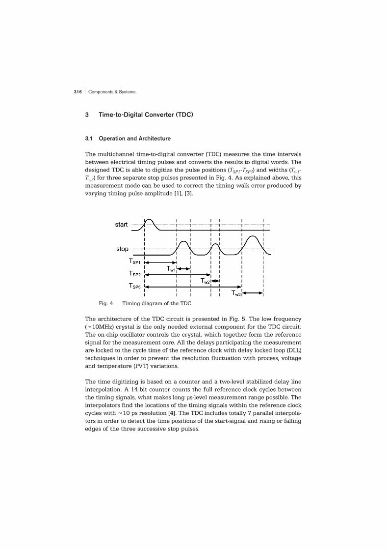
The multichannel time-to-digital converter (TDC) measures the time intervals between electrical timing pulses and converts the results to digital words. The designed TDC is able to digitize the pulse positions (TSP1-TSP3) and widths (Tw1-Tw3) for three separate stop pulses presented in Fig. 4. As explained above, this measurement mode can be used to correct the timing walk error produced by varying timing pulse amplitude [1], [3].
Fig. 4 Timing diagram of the TDC
The architecture of the TDC circuit is presented in Fig. 5. The low frequency (~10MHz) crystal is the only needed external component for the TDC circuit. The on-chip oscillator controls the crystal, which together form the reference signal for the measurement core. All the delays participating the measurement are locked to the cycle time of the reference clock with delay locked loop (DLL) techniques in order to prevent the resolution fluctuation with process, voltage and temperature (PVT) variations.
The time digitizing is based on a counter and a two-level stabilized delay line interpolation. A 14-bit counter counts the full reference clock cycles between the timing signals, what makes long μs-level measurement range possible. The interpolators find the locations of the timing signals within the reference clock cycles with ~10 ps resolution [4]. The TDC includes totally 7 parallel interpola-tors in order to detect the time positions of the start-signal and rising or falling edges of the three successive stop pulses.

317A Laser Scanner Chip Set for Accurate Perception Systems
Fig. 5. Architecture of the TDC circuit
The ALU decodes the raw data and calculates the time intervals between the Start and Stop pulses. The data interface to and from the TDC is a 100MHz SPI (Serial Peripheral Interface), but Ready (measurement ready) and Init (initialize the registers) signals can be used to increase the measurement rate.
4 Measurements
The APD receiver PCB including the avalanche photo diode and both the receiver and the TDC circuits are shown in Fig. 6. The circuits are packaged in plastic QFN32 and QFN36 packages, respectively. Independent SPI interfaces allow the individual control of these devices.
Preliminary measurements have been carried out for the receiver and multi-channel TDC in the laboratory environment. Receiver channel has been meas-ured with the on-board multi-channel TDC. Additionally, TDC performance has been verified in measurements done independently without the receiver chan-nel. The walk error compensation was verified by measuring the compensation curve for the receiver channel. Additionally, the bandwidth, the single-shot resolution, the noise and the power consumption were also measured.

Components & Systems318
Fig. 6. APD is arranged on the bottom side of the PCB APD. All other com-ponents are placed on the top. PCB is designed by SICK. Receiver channel and TDC are developed by the University of Oulu
The receiver circuit, which is shown in Fig. 2 b), was fabricated in 0.35 mm SiGe BiCMOS technology. Fully differential structures have been used in all stages in the receiver channel. The dimensions of the receiver circuit are 1.6 mm x 1.6mm. The power consumption of the receiver channel was 132 mW. The bandwidth and the transimpendance of the receiver channel were 64 kW and 300 MHz, respectively. The rms voltage noise was measured from the output of the analogue output. Input referred rms noise current was about 100 nArms. The minimum acceptable input pulse current of the receiver was about 1 mA (assuming minimum acceptable signal-to-noise ratio SNR is around 10).
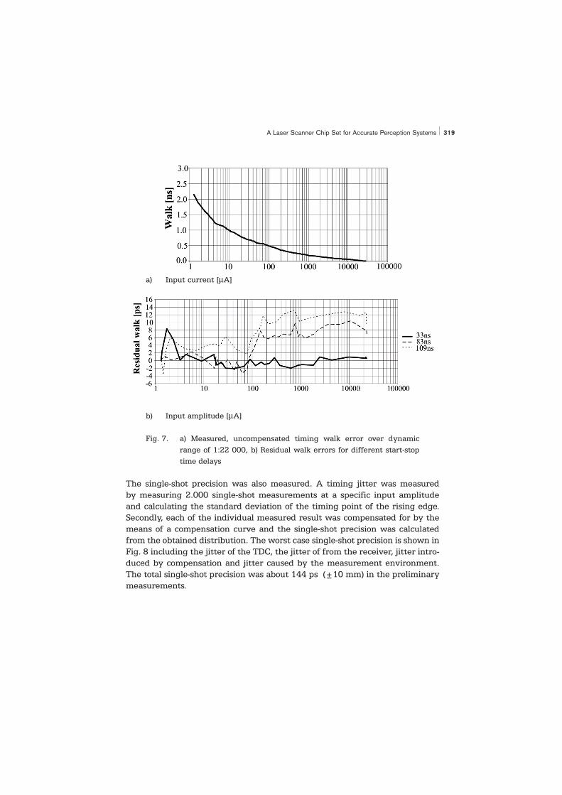
The walk measurements were performed by sweeping the input amplitude over the range of 1: 22.000 where the input pulse amplitude varied from 1 mA to 22 mA. For the compensation curve 2.000 measurements were averaged for each amplitudes. The measured walk error without compensation was about 2.2 ns in total which corresponds to about ± 16 cm is shown in Fig. 7 a). The walk error is compensated for by means of compensation curve measured at calibration measurement. The performance of the walk compensation was verified by measuring residual walk for random input amplitudes over the amplitude range of 1: 22.000. The measured residual walk was less than ±20 ps (<± 4 mm) shown in Fig. 7 b).
319A Laser Scanner Chip Set for Accurate Perception Systems
a) Input current [mA]
b) Input amplitude [mA]
Fig. 7. a) Measured, uncompensated timing walk error over dynamic range of 1:22 000, b) Residual walk errors for different start-stop time delays
The single-shot precision was also measured. A timing jitter was measured by measuring 2.000 single-shot measurements at a specific input amplitude and calculating the standard deviation of the timing point of the rising edge. Secondly, each of the individual measured result was compensated for by the means of a compensation curve and the single-shot precision was calculated from the obtained distribution. The worst case single-shot precision is shown in Fig. 8 including the jitter of the TDC, the jitter of from the receiver, jitter intro-duced by compensation and jitter caused by the measurement environment. The total single-shot precision was about 144 ps (±10 mm) in the preliminary measurements.

Components & Systems320
Fig. 8. Single-shot precision
The TDC circuit was fabricated in 0.35 mm CMOS technology. The dimensions of the circuit are 2.4 mm x 3.7 mm and the total area 8.89 mm2. The power consumption at a 3.3V operating voltage, 20 MHz reference crystal and a 220 MHz internal frequency is 85 mW. The circuit was packaged in plastic QFN36 package.
Fig. 9 describes the measurement performance of the multichannel TDC. One start and three successive stop-pulses with different pulse widths and time intervals over several microseconds were generated with the Tektronix AWG 2021 signal generator. The stop-pulse cable was divided to both stop input channels of the TDC so that a longer coaxial cable was in the stop1 input path than in the stop0 input path. The measurements were repeated 100.000 times in the both measurement modes and the distributions of the results with their average values (m) and standard deviations (s) are presented in Fig. 9. The diagram on top of Fig. 9 shows the time intervals between the start and three successive stop-pulses and is similar in both measurement modes. The diagram above shows the stop-pulse widths. The jitter of the signal generator is present in the results.
5 Conclusions
A chip set was developed for a laser scanner application. The set includes two integrated circuits which cover the receiver channel and the time interval measurement functionalities, respectively. The chip set can detect optical ech-

321A Laser Scanner Chip Set for Accurate Perception Systems
oes with a typical length of 3-4ns in a dynamic range of more than 1:10.000 with an accuracy of better than 100ps. This dynamic range exceeds substan-tially the typical linear range of a high-speed optical receiver and is achieved by realizing the timing walk error compensation in the time domain. Moreover, the chip set may detect simultaneously the time position of the three succes-sive optical pulses.
Fig. 9. Measurements with start and 3 successive stop pulses
Ackknowledgement
Minifaros is a part of the 7th Framework Programme funded by the European Commission. The partners thank the European Commission and the Academy of Finland for supporting the work of this project.
Components & Systems322
References
[1] S. Kurtti, J. Kostamovaara, An integrated laser radar receiver channel utiliz-ing a time-domain walk error compensation scheme, IEEE Transactions on Instrumentation and Measurement, vol. 30, no. 1, pp. 146-157, 2011.
[2] P. Palojärvi, T. Ruotsalainen, J. Kostamovaara, A 250-MHz BiCMOS receiver chan-nel with leading edge timing discrimination, IEEE Journal of Solid-State Circuits, vol. 40, no. 6, pp. 1341-1349, 2005.
[3] J. Nissinen, I Nissinen., J. Kostamovaara, Integrated receiver including both receiver channel and TDC for a pulsed time-of-flight laser rangefinder with cm-level accuracy, IEEE Solid-State Circuits, vol. 44, no. 5, pp. 1486-1497, May 2009.
[4] J.-P. Jansson, V. Koskinen, A. Mäntyniemi, J. Kostamovaara, A multi-channel high precision CMOS time-to-digital conveter for laserscanner based perception systems, IEEE Transactions on Instrumentation and Measurement, accepted for publication 2012.
Sami Kurtti, Jussi-Pekka Jansson, Juha KostamovaaraUniversity of OuluElectronics Laboratory90014 [email protected]@[email protected]
Keywords: LIDAR, optical distance measurement, timing discrimination, time interval measurement, Minifaros