a fast liquid-metal droplet microswitch using ewod …cjmems.seas.ucla.edu/papers/2009 jmems sen...
TRANSCRIPT

174 JOURNAL OF MICROELECTROMECHANICAL SYSTEMS, VOL. 18, NO. 1, FEBRUARY 2009
A Fast Liquid-Metal Droplet Microswitch UsingEWOD-Driven Contact-Line Sliding
Prosenjit Sen and Chang-Jin Kim
Abstract—Liquid-metal (LM) droplet-based MEMS switcheshave mostly been restricted to slow applications until now dueto the following reasons: 1) a relatively large switching gap (dis-tance) needed to accommodate imprecise volumes and locations ofdroplets on the device and 2) lack of high-speed actuation to movethe droplets quickly across the switching gap. To combat theseproblems, we explore switching by sliding the solid–LM–gas triplecontact line rather than the entire droplet. This new approach al-lows us to use a microframe, which not only consistently positionsthe LM droplet but also makes the switching gap less sensitive tothe errors in the deposited-droplet volume, allowing us to designmicroswitches with very small switching gaps (e.g., 10 μm for600 μm-diameter droplets). Furthermore, a study of electrowet-ting-on-dielectric identifies a regime of fast contact-line sliding atthe onset of droplet spreading. By moving the contact line fastacross a small switching distance, we demonstrate a low-latencyLM switch with 60 μs switch-on latency (∼20 times better thanother LM-switch technologies) and better than 5 μs signal rise/falltime, while boasting no contact bounce, as expected from an LMswitch. High power-handling capability and long-term reliabilityare also discussed. [2008-0135]
Index Terms—Contact-line sliding, electrowetting-on-dielectric(EWOD), liquid-metal (LM) microswitch, MEMS switch,microframe.
I. INTRODUCTION
M ICROELECTROMECHANICAL systems (MEMS)switches consist of a moveable micromechanical
element actuated by various mechanisms (e.g., electrostatic[1]–[3], electromagnetic [4], [5], and electrothermal [6], [7])to achieve a short or an open in the signal line. Comparedwith regular (i.e., macroscale) mechanical switches, micro-mechanical switches are fast (switching time on the order ofmicroseconds) and consume small power [1], [8]. Problemsassociated with the solid–solid contact in switches (e.g., contactbounce, arcing, and welding), however, become more importantfor MEMS switches because surfaces play an increased rolein microscale. The resulting contact degradation is one of themost important factors limiting the reliability (operational life)of these devices. In order to solve the problem, following theirmacro counterparts, several microswitch technologies havepursued liquid–solid contact by exploring liquid metals (LMs)
Manuscript received May 21, 2008; revised October 14, 2008. Firstpublished December 22, 2008; current version published February 4, 2009. Thiswork was supported by the DARPA HERMIT program. Subject Editor R. R. A.Syms.
The authors are with the Micro and Nano Manufacturing Laboratory, Uni-versity of California, Los Angeles, CA 90095-1597 USA.
Color versions of one or more of the figures in this paper are available onlineat http://ieeexplore.ieee.org.
Digital Object Identifier 10.1109/JMEMS.2008.2008624
(typically mercury), using less than 1 nL of LM—thousandsof times less than a regular mercury switch. First introduced inthe mid-late 1990s [9], [10], LM-based MEMS switches haverecently demonstrated low contact resistance (0.015 Ω [11]),long life (over 108 cycles [12]), and capability to handle largecurrents (1 A [12]). However, there has not been any approachsuggesting the possibility of fast switching.
In order to implement an LM-contact microswitch, research-ers have investigated two different approaches: the LM-wettedand the LM-actuated microswitch. The first (LM-wetted) ap-proach is to place an LM at the contacts of the solid mov-ing element in MEMS switches, truly mimicking the regularmercury-wetted reed relays. Several implementations have beendeveloped and demonstrated over the last decade. The earliestwas a surface-micromachined polysilicon cantilever (2 μmthick and 2 μm wide) electrostatically actuated in the lateraldirection with a mercury droplet (∼10μm diameter) depositedat the point of contact [13]. A zipper-type actuation was used toachieve large deflection in an attempt to increase the separationforce during switch-off. Another implementation obtained amore stable lateral motion by using a folded beam structuredriven by electrostatic comb actuators [10], reporting a 4 Hzoperating frequency. The switch-on time of these devices de-pends on the mechanical design of the switch and will match theusual solid MEMS switches with similar design. The switch-offtime, however, tends to be much slower because of the largeliquid–solid adhesion and liquid deformation at the contact,compared with the solid–solid contact. Unlike macroscalemercury-wetted reed relays, where structural forces dominate,MEMS switches contain elements in microscale where wettingforces play an important role. Better frequency performance(tens of hertz) was demonstrated [11] by employing an elec-trothermal actuation [11], [14], which generated large-enoughforce (20 mN) to actuate 50 μm-thick beams. Accepting highpower consumption for good switch characteristics, the oper-ating frequency, in this case, was limited by the cooling rateof the beams rather than the dynamics of the beams and theliquid–solid adhesion.
The second (LM-actuated) approach is to move the dropletitself as the switching element. For this purpose, thermal [9],[12], [15] and electrostatic [16], [17] actuations have beenused to demonstrate LM microswitches, while continuous elec-trowetting [18] and electrowetting-on-dielectric (EWOD) [19]have been explored as potential candidates. In [9], an LMdroplet was moved off and on the broken signal electrodes bythermally induced pressure inside a microchannel filled with adielectric liquid. Switching speed was reported to be 10 ms,limited by cooling speed. In [12], an LM slug was broken
1057-7157/$25.00 © 2008 IEEE
Authorized licensed use limited to: IEEE Xplore. Downloaded on February 9, 2009 at 15:12 from IEEE Xplore. Restrictions apply.

SEN AND KIM: FAST LIQUID-METAL DROPLET MICROSWITCH USING EWOD-DRIVEN CONTACT-LINE SLIDING 175
Fig. 1. Microswitch design based on sliding of a LM droplet by EWODactuation. Application of an electric potential on the driving (or pullback)electrode causes the droplet to move to the right (or left). Switching gap, definedas the distance that the contact line needs to travel in order to achieve switching,should be large enough to accommodate the uncertainties in the droplet volumeand position. Fast switching is difficult in this design.
and merged back by thermally induced gas pressure inside anetwork of gas-filled microchannels, reporting a switchingspeed of 0.92 ms. An LM droplet was moved also by electro-static attraction inside a cavity [16] or on the surface of CMOS[17]. The switching speed of these devices was reported to beon the order of 1 ms, limited by the viscous dissipation of theactuated droplet.
There are many aspects of switch characteristics: switchingspeed, signal power, signal frequency, power consumption, op-eration temperature, reliability, device size, etc. One of the mostimportant measures of switching speed is switching latency.Switching latency is defined as the time required for a switchto turn on after actuation has been applied. Slow switching(i.e., large switching latency) has been restricting the use ofLM-based MEMS switches in many applications. In this paper,we first study the challenges in designing low-latency (fast)devices using LM droplets. Then, we propose and develop so-lutions to existing problems before developing the technologiesto demonstrate a low-latency LM microswitch.
II. CHALLENGES IN DESIGNING LOW-LATENCY
SWITCHING OF LM DROPLET
For mechanical relays, switching latency depends on twomain factors. First is the response and moving speed of theactuated switching element, and second is the distance that theswitching element needs to travel in order to achieve switching.Hereafter, this distance is referred to as the switching gap orswitching distance. In order to achieve a low-latency switch,fast actuation mechanism and small switching gap design arerequired. Fig. 1 shows the definition of the switching gapwhile illustrating an LM switch actuated by EWOD. Whenan actuation potential is applied to the driving electrode inthis design, the droplet moves toward the driving electrodeand makes contact with the “signal-out” electrode, and theswitch turns on, as shown in the bottom figure. To turn the
Fig. 2. Typical way the LM droplet is introduced in the microdevice. An errorin the deposited-droplet volume (i.e., error in Rdep) leads to an error in the baseradius (Rbase) of the droplet in the fabricated device. (a) Droplet as deposited.(b) Droplet after device fabrication.
switch off, an actuation potential is applied to the pullbackelectrode, and the droplet returns to its original position, break-ing contact with the signal-out electrode, as shown in thetop figure. However, design and fabrication of a low-latencyswitch based on the schematic shown in Fig. 1 is a formidablechallenge, because consistently obtaining a small actuation gapon the order of 10–100 μm requires droplet deposition andpositioning with high accuracy. Let us consider what affects theaccuracy of the droplet size and the droplet positioning in thedevice.
A. Effect of Droplet-Volume Accuracy
Fig. 2 shows a typical scenario of placing an LM droplet ina microdevice. The droplet is first deposited on the substrateas a spherical cap [see Fig. 2(a)] and then flattened by a topplate [see Fig. 2(b)]. In order to estimate the volume accuracyrequired in the droplet deposition process, variation in the finalflattened-droplet radius due to uncertainty in the deposited-droplet volume needs to be calculated. The volume of thedeposited droplet is given by
V =πR3
dep
3(2 − 3 cos θ + cos3 θ) (1)
where Rdep is the radius of the deposited sessile droplet and θis the contact angle. For the squeezed droplet, the volume canbe calculated as
V = π
g/2∫−g/2
{Rbase +√
r2 − y2 − r sin θ}2dy (2)
where Rbase is the radius of the squeezed droplet and r and gare shown in Fig. 2(b). Contact angle, which is a function ofthe liquid and the substrate surface, remains constant (within
Authorized licensed use limited to: IEEE Xplore. Downloaded on February 9, 2009 at 15:12 from IEEE Xplore. Restrictions apply.

176 JOURNAL OF MICROELECTROMECHANICAL SYSTEMS, VOL. 18, NO. 1, FEBRUARY 2009
Fig. 3. Error in the as-deposited-droplet radius ΔRdep relative to the error inthe squeezed droplet radius ΔRbase for varying droplet sizes and plate gaps.In order achieve the target error range for ΔRbase, a tighter error range is calledfor ΔRdep.
the limits of contact-angle hysteresis). Using the relation r =−g/(2 cos θ), the volume of the squeezed droplet is given by
V = πg
[(Rbase +
g tan θ
2
){Rbase +
g
2
(tan θ
+sin 2θ + π
2 − θ
2 cos2 θ
)}+
g2
12(3 tan2 θ + 2)
](3)
where g is the gap between the plates. Relating (1) and (3)by volume conservation, we can evaluate the expressions for∂V/∂Rbase and ∂V/∂Rdep. Fig. 3 shows the tolerable error inthe as-deposited (spherical) droplet radius ΔRdep relative to atarget error in the deposited (squeezed) droplet radius ΔRbase.A contact angle of 140◦ (mercury on Teflon) is used for cal-culation. For example, in a droplet with a 250 μm base radiusand a 100 μm plate gap (typical values for a device designedfor fast switching), a 5 μm uncertainty in the deposition radiuswill lead to a 10 μm uncertainty in the base radius. Achievinga 5 μm accuracy for a deposition radius of 133 μm is a difficulttask with existing LM-droplet deposition techniques.
B. Accuracy of Deposited-Droplet Volume
Saffer et al. [13] reported microscale mercury depositionusing selective condensation of mercury vapor on photolitho-graphically patterned gold nucleation sites. Mercury vapor re-acts with the thin gold pads to form an amalgam and continuesto condense there preferentially, so LM droplets grow. The finaldroplet size was controlled by varying the deposition time andthe temperature. However, the maximum droplet diameter waslimited to 30 μm due to eventual random nucleation and depo-sition. Although there are no published data on the depositionaccuracy, achieving better than 1 μm accuracy for a 30 μmdroplet is considered difficult in practice [20]. Screen printingof other LM droplets, particularly gallium for its extremely lowvapor pressure even at elevated temperatures (9.31 × 10−36 Pa
Fig. 4. Worst case theoretical deposition error due to quantized deposition asin a droplet jetting device.
at 30 ◦C, which rises to 1 Pa at 1037 ◦C), was demonstrated byTruong [21]. This process also had a limited accuracy due touncertainty in droplet necking and separation from the bulk.
As a part of the current work, a commercial liquid jet-ting system JetLab from MicroFab, Inc. was calibrated forLM-droplet deposition, inspired by the reports of Wan et al.[22]. The system jets small droplets whose diameter mostlydepends on the jetting orifice diameter. Another parameteraffecting the droplet diameter is the jetting voltage waveform.In the experiments, we were able to achieve 30 μm dropletsfrom a 60 μm jetting orifice. Larger diameter droplets wereobtained through multiple depositions at the same location. Wewere able to achieve less than 3% variation in diameter of thedeposited droplets (calculated diameter ∼ 100 μm). Since atypical target droplet is significantly larger than a jetted droplet,high volume accuracy is possible in the deposited droplet. Theworst case theoretical error in the deposited-droplet radius isgiven by
ΔRdep
Rdep=
13
(rjet
Rdep
)3
(4)
where rjet is the radius of a single jetted droplet and Rdep
is the final radius of the droplet obtained through multipledepositions, as shown in Fig. 4. Equation (4) assumes thatthe volume of the individual jetted droplet remains the same.The actual accuracy is, however, determined by the variationin the volume of individual jetted droplets, leading to theobserved ∼3% variation in the final diameter. Even with thiscommercially proven system, a careful calibration is frequentlyneeded to determine the number of droplets required to obtainthe target droplet radius.
C. Effect of Device Fabrication
Another challenge in the formation of a small actuation gapis due to the errors associated with the assembly of the twoplates. In the current design, the plate gap (gap between the
Authorized licensed use limited to: IEEE Xplore. Downloaded on February 9, 2009 at 15:12 from IEEE Xplore. Restrictions apply.
SEN AND KIM: FAST LIQUID-METAL DROPLET MICROSWITCH USING EWOD-DRIVEN CONTACT-LINE SLIDING 177
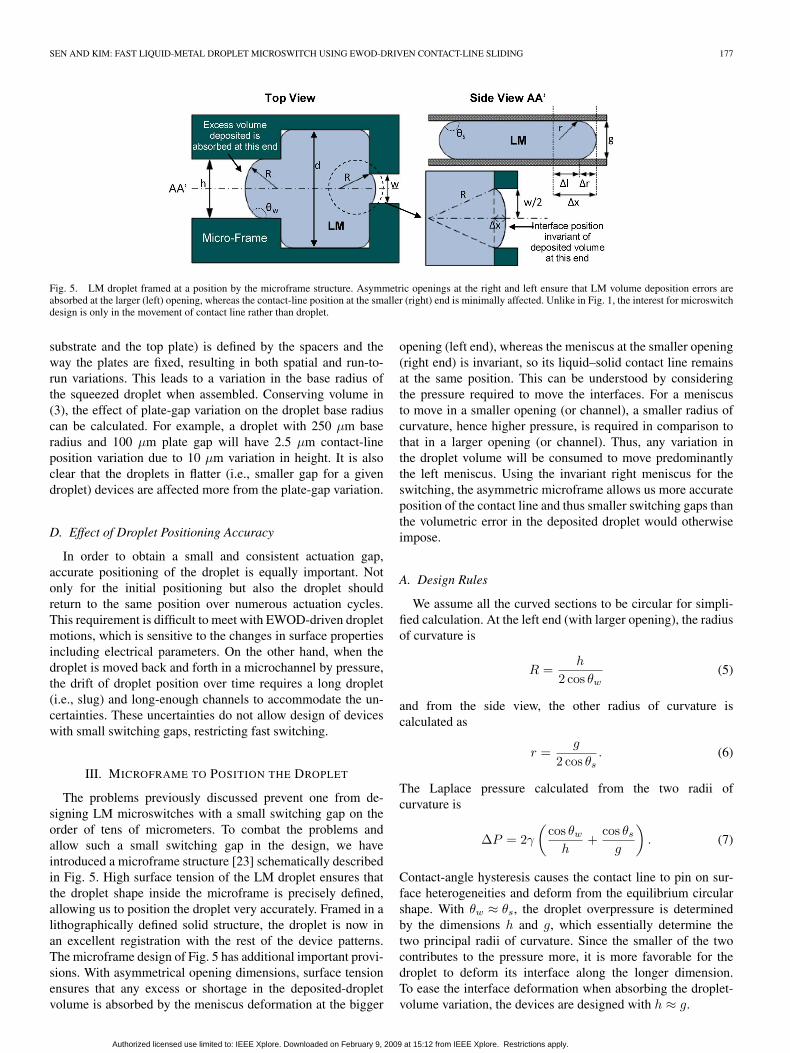
Fig. 5. LM droplet framed at a position by the microframe structure. Asymmetric openings at the right and left ensure that LM volume deposition errors areabsorbed at the larger (left) opening, whereas the contact-line position at the smaller (right) end is minimally affected. Unlike in Fig. 1, the interest for microswitchdesign is only in the movement of contact line rather than droplet.
substrate and the top plate) is defined by the spacers and theway the plates are fixed, resulting in both spatial and run-to-run variations. This leads to a variation in the base radius ofthe squeezed droplet when assembled. Conserving volume in(3), the effect of plate-gap variation on the droplet base radiuscan be calculated. For example, a droplet with 250 μm baseradius and 100 μm plate gap will have 2.5 μm contact-lineposition variation due to 10 μm variation in height. It is alsoclear that the droplets in flatter (i.e., smaller gap for a givendroplet) devices are affected more from the plate-gap variation.
D. Effect of Droplet Positioning Accuracy
In order to obtain a small and consistent actuation gap,accurate positioning of the droplet is equally important. Notonly for the initial positioning but also the droplet shouldreturn to the same position over numerous actuation cycles.This requirement is difficult to meet with EWOD-driven dropletmotions, which is sensitive to the changes in surface propertiesincluding electrical parameters. On the other hand, when thedroplet is moved back and forth in a microchannel by pressure,the drift of droplet position over time requires a long droplet(i.e., slug) and long-enough channels to accommodate the un-certainties. These uncertainties do not allow design of deviceswith small switching gaps, restricting fast switching.
III. MICROFRAME TO POSITION THE DROPLET
The problems previously discussed prevent one from de-signing LM microswitches with a small switching gap on theorder of tens of micrometers. To combat the problems andallow such a small switching gap in the design, we haveintroduced a microframe structure [23] schematically describedin Fig. 5. High surface tension of the LM droplet ensures thatthe droplet shape inside the microframe is precisely defined,allowing us to position the droplet very accurately. Framed in alithographically defined solid structure, the droplet is now inan excellent registration with the rest of the device patterns.The microframe design of Fig. 5 has additional important provi-sions. With asymmetrical opening dimensions, surface tensionensures that any excess or shortage in the deposited-dropletvolume is absorbed by the meniscus deformation at the bigger
opening (left end), whereas the meniscus at the smaller opening(right end) is invariant, so its liquid–solid contact line remainsat the same position. This can be understood by consideringthe pressure required to move the interfaces. For a meniscusto move in a smaller opening (or channel), a smaller radius ofcurvature, hence higher pressure, is required in comparison tothat in a larger opening (or channel). Thus, any variation inthe droplet volume will be consumed to move predominantlythe left meniscus. Using the invariant right meniscus for theswitching, the asymmetric microframe allows us more accurateposition of the contact line and thus smaller switching gaps thanthe volumetric error in the deposited droplet would otherwiseimpose.
A. Design Rules
We assume all the curved sections to be circular for simpli-fied calculation. At the left end (with larger opening), the radiusof curvature is
R =h
2 cos θw(5)
and from the side view, the other radius of curvature iscalculated as
r =g
2 cos θs. (6)
The Laplace pressure calculated from the two radii ofcurvature is
ΔP = 2γ
(cos θw
h+
cos θs
g
). (7)
Contact-angle hysteresis causes the contact line to pin on sur-face heterogeneities and deform from the equilibrium circularshape. With θw ≈ θs, the droplet overpressure is determinedby the dimensions h and g, which essentially determine thetwo principal radii of curvature. Since the smaller of the twocontributes to the pressure more, it is more favorable for thedroplet to deform its interface along the longer dimension.To ease the interface deformation when absorbing the droplet-volume variation, the devices are designed with h ≈ g.
Authorized licensed use limited to: IEEE Xplore. Downloaded on February 9, 2009 at 15:12 from IEEE Xplore. Restrictions apply.

178 JOURNAL OF MICROELECTROMECHANICAL SYSTEMS, VOL. 18, NO. 1, FEBRUARY 2009
Fig. 6. Schematic description of LM-droplet spreading by EWOD actuation.
Since the pressure is constant inside the droplet, the radius ofcurvature at the right opening is equal to that at the left opening.A larger right opening w is preferable for larger overlaps withactuation electrode, which results in a higher driving force.However, in order to achieve the design functionality, w isrestricted by the rule w < h. To calculate the contact-lineposition at the front end, we need to calculate Δx and Δr. Fromthe zoom-in of the top view, Δx is calculated as
Δx = R −√
R2 −(w
2
)2
(8)
where R is calculated from (5) and Δr is calculated from theside view as
Δr =g(sin θs − 1)
2 cos θs. (9)
At the right opening, the position of the contact line from theinner edge of the microframe is obtained as
Δl + Δx − Δr. (10)
B. Effect of Contact-Angle Hysteresis
Contact-angle hysteresis leads to an uncertainty in the con-tact angles. Uncertainty in the contact-line position due tohysteresis can be calculated from (9) as
dΔl
dθ=
dΔx
dθw+
dΔr
dθs. (11)
Now, from (5), we can evaluate
dR
dθw=
h tan θw
2 cos θw(12)
and from (8), we can calculate
dΔx
dR= 1 − 2√
1 −(
w cos θw
h
)2. (13)
Combining (12) and (13), we get the required expression fordΔx/dθw. From (9), we can calculate the error due to hystere-sis on the substrates as
dΔr
dθs=
g(1 − sin θs)2 cos2 θs
. (14)
Therefore, the total uncertainty in the contact-line position is
dΔl
dθ=
h tan θw
2 cos θw
⎧⎨⎩1− 2√
1−(
w cos θw
h
)2
⎫⎬⎭+
g(1 − sin θs)2 cos2 θs
.
(15)
C. Effect of Height Variation
The plate gap g, whether determined by the microframe orseparate spacers, has its uncertainty. Following the techniqueused earlier, we can also evaluate the effect of plate-gap uncer-tainty on the contact-line position
dΔl
dg=
(sin θs − 1)2 cos θs
. (16)
It is important to note that variation in g only affects Δr and hasno effect on Δx, which is dependent on the lithographicallydefined horizontal dimensions. For a mercury-on-Teflon sys-tem, the ratio Δr/Δg is approximately 0.23, suggesting that a10 μm error in the plate gap will lead to approximately 2.3 μmerror in the contact-line position.
IV. EWOD-DRIVEN CONTACT-LINE SLIDING
FOR FAST SWITCHING
Consider the configuration shown in Fig. 6. A droplet sitson the dielectric with a conductive electrode underneath. Ap-plication of an electric potential makes the surface tension atthe liquid–solid interface to drop, reducing the contact angleand causing the droplet to spread [24]. The phenomenon isexpressed mathematically as
cos θ = cos θ0 +cV 2
2γ
Rbase
Rbase,0V=
{2 − 3 cos θ0 + cos3 θ0
2 − 3 cos θ + cos3 θ
} 13
× sin θ
sin θ0(17)
where Rbase is the radius of the liquid–solid contact area.Using (17) and taking contact-angle saturation into consider-ation, we can predict the radius of the LM droplet for anygiven voltage. This spreading of the droplet is the basic mo-tion for many electric-field-based actuations. In the case ofEWOD-based droplet translation [25]–[27], spreading takesplace first at the leading edge before the overall movement.Thus, in order to achieve a low-latency (fast) switch, we pro-pose to use this contact-line spreading for switching rather thanthe movement of the droplet shown in Fig. 1.
Authorized licensed use limited to: IEEE Xplore. Downloaded on February 9, 2009 at 15:12 from IEEE Xplore. Restrictions apply.

SEN AND KIM: FAST LIQUID-METAL DROPLET MICROSWITCH USING EWOD-DRIVEN CONTACT-LINE SLIDING 179
Fig. 7. Instrumentation to study the droplet spreading dynamics duringEWOD. A computer uses an NI-DAQ card to simultaneously generate theactuation signal and trigger the high-speed camera.
Fig. 8. Measured contact-angle and contact-line movements for dropletdynamics for different EWOD actuation voltages.
To design a fast switch, it was necessary to measure theactuation speed of the droplet interface when actuated usingEWOD. For this purpose, an experimental setup was developed(see Fig. 7) to capture and study the dynamics of a droplet actu-ated by EWOD using a high-speed camera (Phantom v7.3 fromVision Research). The camera was operated at 10 000 framesper second, which allowed a maximum resolution of 600 ×480 pixels. For droplet actuation, a computer was used togenerate step voltages of varying magnitudes with the aid of amultifunctional NI-DAQ card. This signal was amplified usingan amplifier (Trek Model 601C) having a slew rate of 50 V/μs.The camera was triggered simultaneously by a digital IO porton the DAQ card.
All the captured images were analyzed using the canny edgedetection algorithm with subpixel edge detection [28] to extractthe droplet shape. Intersection of the extracted curve with themanually defined baseline is used to determine the base radiusand the contact angle. The measured data are shown in Fig. 8.For a droplet of radius ∼1 mm, the contact angle changesrapidly during the first 250 μs and stabilizes near its finalvalue, estimated by (17), in 500 μs. For an actuation signal of100 VDC, the contact line moves very fast with speeds up to0.5 m/s during the initial period of 0–200 μs when the contactangle is still decreasing noticeably. However, the contact line
slows down rapidly when the contact angle nears the finalvalue. Contact-line oscillation due to the formation of capillarywaves in the meniscus above the contact line was also observedat higher actuation voltages. For fast switching, the devicedesign will utilize the contact-line spreading during the initialregime only.
V. DESIGN OF A FAST-SWITCHING DEVICE
From the contact-line velocity data, design of switches with20 μs switching latency seems possible if a switching gapof 10 μm is used. However, for a freely placed droplet withradius of hundreds of micrometers, this would require betterthan 4% control over deposition radius and position, which isa difficult task for existing LM-droplet deposition techniques.The situation is worsened when positional uncertainty of thecontact line due to contact-angle hysteresis is taken into con-sideration. We introduced the use of microframe structures toovercome the variation in the deposited-droplet volume and thepoor positioning of the droplet on the device surface. Here,the EWOD-based actuation and the microframe technology arecombined to design a low-latency switch. Two different designswere developed. The first design uses a symmetric microframestructure, providing larger actuation force but limited tolerancefor volume error. The second design uses the asymmetricmicroframe structure discussed in Section III, providing a bettertolerance for volume error but lower actuation force.
A. Symmetric Microframe Design
The schematic of the symmetric switch design is shown inFig. 9 for the OFF state (top left and middle left) and the ON
state (top right and middle right), viewed from different angles.The uncertainty due to contact-angle hysteresis is reduced whenthe droplet is switched in the microframe. For a given dropletvolume, any variation in the base radius (contact-line position)due to hysteresis is accompanied by a change in the overallradius of the droplet. However, since the microframe restrictschange in the radius of the droplet, any variation in the contact-line position due to hysteresis can only be possible through avariation in the local curvature between the posts of the frame.The variation in the local curvature gives rise to a restoringLaplace pressure, which resists the change in the contact-lineposition. Switches were designed for droplets of 300 μm spher-ical radius and switching gaps of 10 and 20 μm. On applicationof the actuation potential, the contact line spreads and makescontact with the signal electrode, as shown best with the cross-sectional views in Fig. 9 (middle row). When the actuationpotential is removed, the interface contracts and breaks contactwith the signal electrode. The bottom photographs in Fig. 9 areto better illustrate the three-dimensional nature of a droplet in amicroframe as well as on the droplet signal electrode.
B. Asymmetric Microframe Design
Fig. 10 shows the asymmetrical design. The microframedesign is based on the design rules discussed earlier. When apotential is applied to the driving electrode, the contact lineon it slides and makes connection with the signal electrode,
Authorized licensed use limited to: IEEE Xplore. Downloaded on February 9, 2009 at 15:12 from IEEE Xplore. Restrictions apply.

180 JOURNAL OF MICROELECTROMECHANICAL SYSTEMS, VOL. 18, NO. 1, FEBRUARY 2009
Fig. 9. Schematic of the LM switch using a symmetric microframe. (a) Top view. (b) Cross-sectional view. (c) Perspective view.
Fig. 10. Schematic top view of the LM switch using an asymmetric microframe.
as seen in Fig. 10. Devices were designed with 400 μm-tallmicroframe. The left (larger) opening is designed to be 400 μm,and the right (smaller) opening is 250 or 300 μm. Table I showsthe effect of contact-angle hysteresis and plate-gap variationon device design. A 5◦ uncertainty in the contact angle fromcontact-angle hysteresis leads to ∼6 μm of uncertainty in thecontact-line position. The effect of plate-gap variation is lesssevere; a 10 μm error in the gap leads to ∼2μm error in the
contact-line position. To accommodate these uncertainties, theLM microswitches were designed with an actuation gap of atleast 10 μm.
C. Vibrational Stability
1) Horizontal Stability: For the microframe design shownin Fig. 5, the droplet will escape from the left (larger) opening
Authorized licensed use limited to: IEEE Xplore. Downloaded on February 9, 2009 at 15:12 from IEEE Xplore. Restrictions apply.

SEN AND KIM: FAST LIQUID-METAL DROPLET MICROSWITCH USING EWOD-DRIVEN CONTACT-LINE SLIDING 181
TABLE ICALCULATION OF DESIGN PARAMETERS. EFFECT OF CONTACT-ANGLE
HYSTERESIS AND MICROFRAME THICKNESS VARIATION ON
CONTACT-LINE POSITION
most easily. The excess pressure required for the droplet toescape is given by
ΔP = 2γ
{(cos θr − cos θa
g
)+
(cos θr
d− cos θa
h
)}
(18)
where d is the reservoir dimension, g is the plate gap, and θa andθr are the advancing and receding contact angles, respectively.The pressure generated due to inertia is
ΔPm =ma
hg∼= ρd2α
h(19)
where α is the acceleration. From (18) and (19), the escapeacceleration is given by
α =2γh
ρd2
{(cos θr − cos θα
g
)+
(cos θr
d− cos θα
h
)}.
(20)
This microframe design provides stability to the mercurydroplet against an inertial shock of ∼16.5 G in the horizontaldirection.
2) Vertical Stability: A vertical acceleration will cause thedroplet to spread or retract and cause unintended switching. Theinterface will be pinned until the angles at one of the substratesreach the advancing angle and that at the other substrate reachesthe receding angle. The force is given by
F = 4dy(cos θr − cos θa). (21)
Equating it with the inertial force, the critical acceleration is
α =4γ
ρdg(cos θr − cos θa). (22)
For the current design, the critical acceleration at which thecontact line starts to move is ∼16 G. Vibrational stability wouldbe improved, along with switching speed, when fabricationin an advanced facility allows further miniaturization of thedevice.
VI. DEVICE FABRICATION, TESTING, AND RESULTS
A. Fabrication
Fabrication is of five lithography steps, as described inFig. 11. Chromium is deposited by E-beam (1000 Å thick) andwet etched to form the actuation electrodes. A 3500 Å siliconnitride, which leads to a reasonable actuation voltage with-out dielectric breakdown, is deposited using plasma-enhancedchemical vapor deposition and patterned by reactive ion etchingto open the contact pads. Lift-off nickel is used to form thesignal electrodes. Nickel is used because it is one of the fewmetals that do not chemically react with mercury. Although anontoxic LM with a low vapor pressure will eventually be used(e.g., Galinstan of Geratherm Medical AG, Germany), mercurywas used in all the results reported here because of the conve-nience of working with glass substrates. Chromium is anotheroption for the signal electrode, but its surface oxidation leadsto excessive contact resistance. A multicoat SU-8 process [29]is used to form 400 μm-high microframe structures. The longcontinuous exposure required for the thick SU-8 causes surfacehardening of the resist due to heating, as seen in Fig. 12. Tosolve this problem, the total exposure time was broken in stepsof 30 s, followed by 30 s of cooling. After the development ofSU-8 structures, a hydrophobic layer (2000 Å Teflon) is spincoated. The hydrophobic layer is patterned lithographically byadding a surfactant to the PR and is etched using O2 plasma.In the final step, a 600 μm-diameter mercury droplet is placedmanually on the device.
B. Contact-Line Pinning and Contact Redesign
Initial switch designs, having a signal electrode with a flatend, as seen in Fig. 1 and the top-left photograph of Fig. 13,did not produce successful switches. Although it was critical toobserve the contact-line sliding for an accurate diagnosis of thefailure, the contact line below the opaque mercury beading onthe surface was not visible. To combat the problem, the sameswitch was temporarily fabricated with transparent indium tinoxide (ITO) electrodes instead of nickel, so the contact linecould be viewed from the bottom through the glass substrate.It was seen that, for flat electrodes, even when the interface hadfully extended (at 160 VDC), the interface was pinned at thebeginning (left) end of the signal electrode, and the LM failed tomake contact on the signal electrode. The moving LM interfacehas to overcome a stiction force that is proportional to thewidth of the contact line. Once the problem was diagnosed, thissituation was rectified by making the end of the signal electrodesharp and pointed, as shown in the bottom-left photograph ofFig. 13. Facing less pinning force due to reduced tip width, thecontact line was able to move over the electrode at 80 VDC.
C. Switching Result
The switch test was conducted using a common groundconfiguration. A computer was used to generate a step signal,which was amplified to form the actuation voltage. A separatedc source was used to evaluate the switch performance. Thelowest switch-on voltage observed was 75 VDC with switch-off
Authorized licensed use limited to: IEEE Xplore. Downloaded on February 9, 2009 at 15:12 from IEEE Xplore. Restrictions apply.

182 JOURNAL OF MICROELECTROMECHANICAL SYSTEMS, VOL. 18, NO. 1, FEBRUARY 2009
Fig. 11. Fabrication process of the microswitch in this paper. The positions of sections AA′ and BB′ are shown in Fig. 11.
Fig. 12. SEM micrograph of the fabricated devices showing microframe structures. A stepped exposure process was developed to eliminate the lips on the frametop. (a) Surface hardening causes the overhanging structure. (b) Stepped exposure to solve the surface hardening problem.
voltage of 45 VDC. Larger switch-on voltages were due tothe stiction force (from the signal electrode) that the interfacehad to overcome so that the LM droplet made contact with
the electrode. However, a device-to-device variation in theminimum switch-on voltage was observed. This variation isattributed to the uncertainty due to contact-angle hysteresis.
Authorized licensed use limited to: IEEE Xplore. Downloaded on February 9, 2009 at 15:12 from IEEE Xplore. Restrictions apply.

SEN AND KIM: FAST LIQUID-METAL DROPLET MICROSWITCH USING EWOD-DRIVEN CONTACT-LINE SLIDING 183
Fig. 13. Problem of (top row) contact-line pinning at the left end of the signal electrode was solved by making the (bottom row) end pointed (sharp). The imageswere taken from below through the glass substrate by fabricating the device with ITO electrodes temporarily.
Switching latency tests were performed using 100 VDC ac-tuation signal with 10 ms pitch and 10% duty cycle. Switchingdata were captured using an oscilloscope. The captured dataare shown in Fig. 14. The sliding motion of the LM contactline ensures bounce-free switching, as shown in the data. Themeasured switch-on latency was 60 μs, and switch-off latencywas 150 μs. The distance which the LM-droplet interfacetravels when switched off depends on the switch design. Forthe current device, it was designed to be 50 μm, which explainsthe larger switch-off latency. The devices were designed withthis large switch-off distance to prevent switch bounce dueto meniscus oscillations caused by the capillary waves. Themeasured signal rise and fall times were smaller than 5 μs.
The contact resistance was obtained using a four-pointmeasurement technique. The measured contact resistance was2.35 Ω for a 50μm × 50μm Ni–Hg contact. There was signifi-cant device–device variation in the measured contact resistance,confirming the suspicion that the droplet interface was oxidizedand contaminated. Droplet deposition and testing in an inertenvironment will provide a better estimation of the true contactresistance in the future. Unlike solid–solid contact switches,larger contact area for a liquid–solid contact should lead tosmaller contact resistance [30] for a given actuation voltage.The power-handling capability of devices was also tested. Thedevice was able to hot-switch 1 W of power without any visualdamage. However, electrode burnout was observed when 4 Wwas attempted. Once the device failed, the contact resistanceincreased to 1.5 kΩ. Much higher power is expected to beswitched once the contact resistance is lowered by fabricatingand packaging the device in an inert environment.
D. Long-Term Reliability Against Dielectric Charging
Although the first mode of failure due to short-term dielectriccharging was solved by biasing the mercury positive [19], aproblem of long-term dielectric charging still exists and willlead to device failure like all other capacitively driven MEMSswitches. To study the long-term effect of dielectric chargingon EWOD actuation of an LM droplet, the device was actuatedusing high voltage (80 VDC) to simulate switching. Afterthe device has been actuated for 100 cycles, the capacitance
Fig. 14. Measured switching profile of actuation versus signal voltages. Thetime-magnified profile in the bottom graph shows the switch latencies andbounceless switching.
between the LM and the driving electrode was measured whileboth the electrodes are grounded. Trapped charges will inducecharges in the LM interface, causing the LM surface energy
Authorized licensed use limited to: IEEE Xplore. Downloaded on February 9, 2009 at 15:12 from IEEE Xplore. Restrictions apply.

184 JOURNAL OF MICROELECTROMECHANICAL SYSTEMS, VOL. 18, NO. 1, FEBRUARY 2009
Fig. 15. Instrumentation of long-term dielectric charging test.
Fig. 16. Dielectric charging and its effect on actuation mechanism overrepeated cycles.
to change and the droplet to spread with an increase in thecontact area. Capacitance measurement gives an estimate of thedroplet contact area and is an indicator of the effect of dielectriccharging on the actuation technique. To measure capacitance, asmall signal ac voltage was applied, and the voltage magnitudedifference in an RC circuit configuration (see Fig. 15) wasmeasured using an oscilloscope. Fig. 16 shows the effect ofactuation polarity on device reliability up to 105 cycles. Theconfiguration with negative polarity on the LM droplet failedimmediately due to severe charging of the dielectric and anincrease in the droplet contact area. Positive-polarity actuationperformed much better. Even though there was a slight increasein the droplet contact area, the devices were much below theswitch failure limit, defined as the droplet radius at which theswitch would remain on due to dielectric charging.
VII. CONCLUSION
We have presented a fast LM-based micromechanical switch,which used a microframe for accurate positioning of the dropletand its meniscus and EWOD for fast actuation of its triplecontact line. The microframe technology solved the problem
in depositing an accurate volume of droplets at exact locationson the device surface, which has been limiting the use of LMdroplets in low-latency applications. Droplet spreading dynam-ics was studied using a high-speed camera. A fast-movingregime of the triple-line spreading was identified and used forthe switch design. The switching latencies obtained (60 μs onand 150 μs off) were approximately 20 times better than that ofthe previously reported LM-droplet switches. The rise and falltimes for the switched signal were better than 5 μs.
A liquid–solid contact means no switch bounce or contactdegradation with use. Even without any design considerationfor power handling, current switches could hot-switch 1 Wof power. Since the LM droplet is two orders of magnitudethicker than the electrodes near the contact in typical MEMSswitches, much larger power-handling capability is expected.Such a full capability is expected once the packaging technol-ogy is advanced and the contact resistances are reduced. Long-term device reliability has also been discussed along with apreliminary test up to 105 cycles, with full tests being deferreduntil the hermetic packaging would prevent surface oxidationand evaporation of the LM droplet [31].
ACKNOWLEDGMENT
The authors would like to thank Prof. A. Feinerman andDr. Z. Wanfrom of The University of Chicago for their help-ful discussions on the JetLab system for mercury dropletdeposition.
REFERENCES
[1] R. Chan, R. Lesnick, D. Becher, and M. Feng, “Low-actuation voltage RFMEMS shunt switch with cold switching lifetime of seven billion cycles,”J. Microelectromech. Syst., vol. 12, no. 5, pp. 713–719, Oct. 2003.
[2] K. E. Petersen, “Micromechanical membrane switches on silicon,” IBMJ. Res. Develop., vol. 23, no. 4, pp. 376–385, Jul. 1979.
[3] C. L. Goldsmith, Z. Yao, S. Eshelman, and D. Denniston, “Performanceof low-loss RF MEMS capacitive switches,” IEEE Microw. Guided WaveLett., vol. 8, no. 8, pp. 269–271, Aug. 1998.
[4] W. P. Taylor, O. Brand, and M. G. Allen, “Fully integrated magneticallyactuated micromachined relays,” J. Microelectromech. Syst., vol. 7, no. 2,pp. 181–191, Jun. 1998.
[5] M. Ruan, J. Shen, and C. B. Wheeler, “Latching micromagnetic relays,”J. Microelectromech. Syst., vol. 10, no. 4, pp. 511–517, Dec. 2001.
[6] J. Qui, “A electrothermally-actuated bistable MEMS relay for powerapplications,” Ph.D. dissertation, MIT, Cambridge, MA, 2003.
[7] Y. Wang, Z. Li, D. T. McCormick, and N. C. Tien, “A micromachinedRF microrelay with electrothermal actuation,” Sens. Actuators A, Phys.,vol. 103, no. 1/2, pp. 231–236, Jan. 2003.
Authorized licensed use limited to: IEEE Xplore. Downloaded on February 9, 2009 at 15:12 from IEEE Xplore. Restrictions apply.

SEN AND KIM: FAST LIQUID-METAL DROPLET MICROSWITCH USING EWOD-DRIVEN CONTACT-LINE SLIDING 185
[8] G. M. Rebeiz, RF MEMS Theory, Design, and Technology, 1st ed.Hoboken, NJ: Wiley Interscience, 2003.
[9] J. Simon, S. Saffer, and C.-J. Kim, “A liquid-filled microrelay with amoving mercury microdrop,” J. Microelectromech. Syst., vol. 6, no. 3,pp. 208–216, Sep. 1997.
[10] J. Simon, S. Saffer, F. Sherman, and C.-J. Kim, “Lateral polysilicon mi-crorelays with a mercury microdrop contact,” IEEE Trans. Ind. Electron.,vol. 45, no. 6, pp. 854–860, Dec. 1998.
[11] A. Cao, P. Yuen, and L. Lin, “Microrelays with bidirectionalelectrothermal electromagnetic actuators and liquid metal wetted con-tacts,” J. Microelectromech. Syst., vol. 16, no. 3, pp. 700–708, Jun. 2007.
[12] Y. Kondoh, T. Takenaka, T. Hidaka, G. Tejima, Y. Kaneko, and M. Saitoh,“High-reliability, high-performance RF micromachined switch usingliquid metal,” J. Microelectromech. Syst., vol. 14, no. 2, pp. 214–220,Apr. 2005.
[13] S. Saffer, J. Simon, and C.-J. Kim, “Mercury-contact switching with gap-closing microcantilever,” in Proc. Micromachined Devices Compon. II,Austin, TX, Oct. 1996, pp. 204–209.
[14] A. Cao, J. B. Kim, T. Tsao, and L. Lin, “A bi-directional electrothermalelectromagnetic actuator,” in Proc. IEEE Conf. Micro Electro Mech. Syst.,Maastricht, The Netherlands, Jan. 2004, pp. 450–453.
[15] J. Simon, S. Saffer, and C.-J. Kim, “A micromechanical relay with athermally-driven mercury micro-drop,” in Proc. IEEE Conf. Micro ElectroMech. Syst., San Diego, CA, Feb. 1996, pp. 515–520.
[16] J. Kim, W. Shen, L. Latorre, and C.-J. Kim, “A micromechanical switchwith electrostatically driven liquid-metal droplet,” Sens. Actuators A,Phys., vol. 97/98, pp. 672–679, 2002.
[17] W. Shen, R. T. Edwards, and C.-J. Kim, “Electrostatically actuated metal-droplet microswitches integrated on CMOS chip,” J. Microelectromech.Syst., vol. 15, no. 4, pp. 879–889, Aug. 2006.
[18] J. Lee and C.-J. Kim, “Surface-tension-driven microactuation based oncontinuous electrowetting,” J. Microelectromech. Syst., vol. 9, no. 2,pp. 171–180, Jun. 2000.
[19] P. Sen and C.-J. Kim, “Electrostatic fringe-field actuation for liquid-metaldroplets,” in Proc. 13th Int. Conf. Solid-State Sens., Actuators, Microsyst.,Seoul, Korea, Jun. 2005, pp. 705–708.
[20] Communication with J. Kim, 2005.[21] T. D. Truong, “Selective deposition of micro scale liquid gallium alloy
droplets,” M.S. thesis, Univ. California (UCLA), Los Angeles, CA, 2000.[22] Z. Wan, H. Zeng, and A. Feinerman, “Area-tunable micromirror based
on electrowetting actuation of liquid-metal droplets,” Appl. Phys. Lett.,vol. 89, no. 20, p. 201 107, Nov. 2006.
[23] P. Sen and C.-J. Kim, “A fast liquid-metal droplet switch using EWOD,”in Proc. IEEE Int. Conf. Micro Electro Mech. Syst., Kobe, Japan,Jan. 2007, pp. 767–770.
[24] H. Moon, S.-K. Cho, R. L. Garrell, and C.-J. Kim, “Lowvoltage electrowetting-on-dielectric,” J. Appl. Phys., vol. 92, no. 7,pp. 4080–4087, Oct. 2002.
[25] S. K. Cho, H. Moon, and C.-J. Kim, “Creating, transporting,cutting, and merging liquid droplets by electrowetting-based actuation fordigital microfluidic circuits,” J. Microelectromech. Syst., vol. 12, no. 1,pp. 70–80, Feb. 2003.
[26] J. Lee, H. Moon, J. Fowler, T. Schoellhammer, and C.-J. Kim, “Electro-wetting and electrowetting-on-dielectric for microscale liquid han-dling,” Sens. Actuators A, Phys., vol. 95, no. 2/3, pp. 259–268,Jan. 2002.
[27] M. G. Pollack, R. B. Fair, and A. D. Shenderov, “Electrowetting-basedactuation of liquid droplets for microfluidic applications,” Appl. Phys.Lett., vol. 77, no. 11, pp. 1725–1726, Sep. 2000.
[28] J. Canny, “A computational approach to edge detection,” IEEETrans. Pattern Anal. Mach. Intell., vol. PAMI-8, no. 6, pp. 679–698,Nov. 1986.
[29] A. Mata, A. J. Fleischman, and S. Roy, “Fabrication of multi-layer SU-8microstructures,” J. Micromech. Microeng., vol. 16, no. 2, pp. 276–284,Feb. 2006.
[30] R. S. Timsit, “The true area of contact at a liquid metal–solid interface,”Appl. Phys. Lett., vol. 40, no. 5, pp. 379–381, Mar. 1982.
[31] T. G. Winter, “The evaporation of a drop of mercury,” Amer. J. Phys.,vol. 71, no. 8, pp. 783–786, Feb. 2003.
Prosenjit Sen was born in Calcutta, India, in 1978.He received the B.Tech. degree in manufacturingscience and engineering from Indian Institute ofTechnology, Kharagpur, India, in 2000, and the Ph.D.degree in mechanical engineering from the Univer-sity of California, Los Angeles, in 2007.
He is currently with the Micro and Nano Manufac-turing Laboratory, University of California. His re-search interests include microfludic systems, dropletdynamics, liquid-metal-based RF MEMS, and re-liability of electrowetting-on-dielectric (EWOD)
devices.Dr. Sen was the recipient of the Institute Silver Medal from the Indian
Institute of Technology.
Chang-Jin “CJ” Kim received the B.S. degree fromSeoul National University, Seoul, Korea, the M.S.degree from Iowa State University, Ames, and thePh.D. degree in mechanical engineering in 1991from the University of California, Berkeley.
In 1993, he joined the faculty of the Universityof California, Los Angeles (UCLA), where he hasdeveloped several MEMS courses and establisheda MEMS Ph.D. major field in the Department ofMechanical and Aerospace Engineering. He is cur-rently directing the Micro and Nano Manufacturing
Laboratory and is also an IRG Leader for the NASA-supported Institute for CellMimetic Space Exploration (CMISE) and a founding member of the CaliforniaNanoSystems Institute (CNSI), UCLA. He is also active in the commercialsector, as board member, scientific advisor, consultant, and co-founder ofstart-up companies. He currently serves as a Subject Editor for the JOURNAL
OF MICROELECTROMECHANICAL SYSTEMS and on the Editorial AdvisoryBoard for the IEEJ Transactions on Electrical and Electronic Engineering. Hisresearch interests include MEMS and nanotechnology, including the design andfabrication of micro/nanostructures, actuators, and systems, with a focus on theuse of surface tension.
Prof. Kim has served on numerous technical program committees, includingthose of the Transducers Conference and the IEEE MEMS Conference, andon the U.S. Army Science Board as Consultant. He is currently chairingthe Devices and Systems Committee of the ASME Nanotechnology Instituteand serving on the National Academies Panel on Benchmarking the ResearchCompetitiveness of the U.S. in Mechanical Engineering. He was the recipientof the TRW Outstanding Young Teacher Award, NSF CAREER Award, ALAAchievement Award, Samueli Outstanding Teaching Award, and GraduateResearch Excellence Award from Iowa State University.
Authorized licensed use limited to: IEEE Xplore. Downloaded on February 9, 2009 at 15:12 from IEEE Xplore. Restrictions apply.