column-row addressable electric microswitch arrays and sensor
TRANSCRIPT
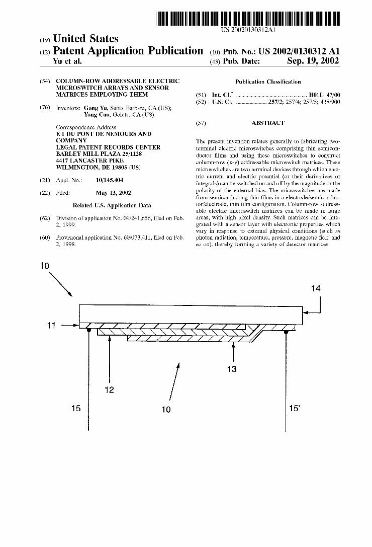
US 20020130312A1
(12) Patent Application Publication (10) Pub. No.: US 2002/0130312 A1 (19) United States
Yu et al. (43) Pub. Date: Sep. 19, 2002
(54) COLUMN-ROW ADDRESSABLE ELECTRIC MICROSWITCH ARRAYS AND SENSOR MATRICES EMPLOYING THEM
(76) Inventors: Gang Yu, Santa Barbara, CA (US); Yong Cao, Goleta, CA (US)
Correspondence Address: E I DU PONT DE NEMOURS AND COMPANY LEGAL PATENT RECORDS CENTER BARLEY MILL PLAZA 25/1128 4417 LANCASTER PIKE WILMINGTON, DE 19805 (US)
(21) Appl. No.: 10/145,404
(22) Filed: May 13, 2002
Related US. Application Data
(62) Division of application No. 09/241,656, ?led on Feb. 2, 1999.
(60) Provisional application No. 60/073,411, ?led on Feb. 2, 1998.
10
Publication Classi?cation
1 nt. . ................................................... .. 7 5 I C] 7 H01L 4 /00 (52) US. Cl. ..................... .. 257/2; 257/4; 257/5; 438/900
(57) ABSTRACT
The present invention relates generally to fabricating tWo terminal electric microsWitches comprising thin semicon ductor ?lms and using these microsWitches to construct column-roW (x-y) addressable microsWitch matrices. These microsWitches are tWo terminal devices through Which elec tric current and electric potential (or their derivatives or integrals) can be switched on and off by the magnitude or the polarity of the external bias. The microsWitches are made from semiconducting thin ?lms in a electrode/semiconduc tor/electrode, thin ?lm con?guration. Column-roW address able electric microsWitch matrices can be made in large areas, With high pixel density. Such matrices can be inte grated With a sensor layer With electronic properties Which vary in response to external physical conditions (such as photon radiation, temperature, pressure, magnetic ?eld and so on), thereby forming a variety of detector matrices.
15 1O 15'
Patent Application Publication Sep. 19, 2002 Sheet 1 0f 12 US 2002/0130312 A1
10
w
NW... w / /\/ /\/ \/ /\/
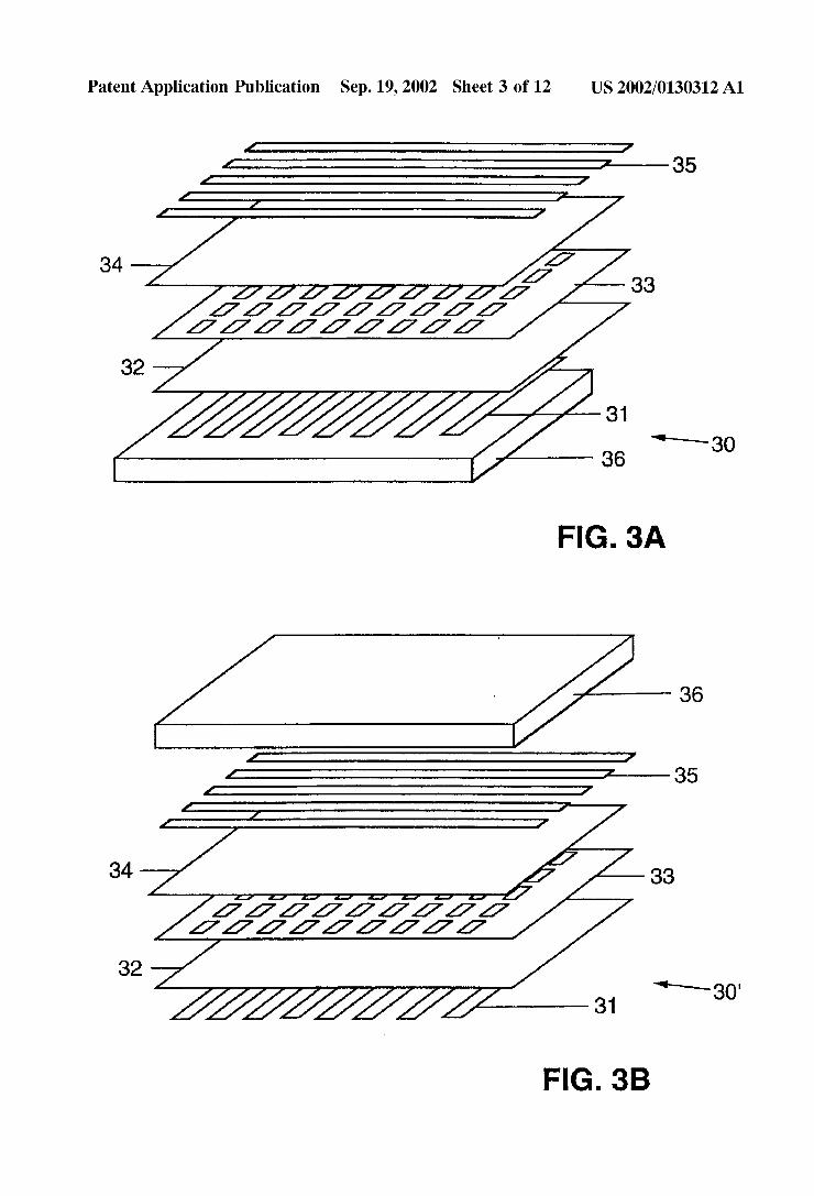
/\/ / 0 \/ 1
/
\/ /\/ /.\V \
{All m /\
FIG. 1
Patent Application Publication Sep. 19, 2002 Sheet 2 0f 12 US 2002/0130312 A1
/////////////~\21 >\\\\\\\\\\\\\\\ 22 ////////////////////;\23 \ \\\\\\\\\\\\\\\\\\\\\\\ 24 20
FIG. 2A 26 \
\25
&\\\\\\\\\\\\\\\\\\\\\24 /////////////////////\23 \ ,\\\\\\\\\\\\\\ \22 20' /////////////\21
FIG. 2B
SWITCH
+
SENSOR
FIG. 2C
Patent Application Publication Sep. 19, 2002 Sheet 3 0f 12 US 2002/0130312 A1
33
36 ‘\30
FIG. 3A
/ v % 36 , ’ I I 35
34 7/ 33 uuuagriaruu
32
?i/MX 31 FIG. 38
Patent Application Publication Sep. 19, 2002 Sheet 4 0f 12 US 2002/0130312 A1
ffffff‘ffffffff ffffffffffffff ffffffffffff‘ff ffffffffffffff ff‘ffffffffffff ffffffffffffff ffffffffffffff 12345678
FIG. 4
Patent Application Publication
CURRENT (mA/cm2)
Rr
Sep. 19, 2002 Sheet 5 0f 12 US 2002/0130312 A1
102 I I I l I I I I I I I I I T I ‘ l I I {—l' I I
100
10'2
O 2 4 6
BIAS [V]
FIG. 5A
I I I I I I I I l
a", I I I l I I I I I I I l l I I I I I I I l I l I
0 1 2 3 4 5
BIAS[V]
FIG. 5B
Patent Application Publication Sep. 19, 2002 Sheet 6 0f 12 US 2002/0130312 A1
10-5 flllll|lpllI||ll I
3? -7
E UJ -9 cE10 cc :3
910'11
10"13 I 1L. -6 -4 -2 O 2 4 6
B|AS[V]
F|G.6A
106m. 0 5
E10 E104 5 3
Q10-2 & i- 101 8 (1:100
10-1I|l1l||||.lllllllLlllljlLlllll 0 1 2 3 4 5 6
BIAS[V]
FIG. 6B
Patent Application Publication
CURRENT (mA/cm 2)
Rr
Sep. 19, 2002 Sheet 7 0f 12 US 2002/0130312 A1
BIAS (v)
FIG. 7A
I I I I I I l I I I I I I l I I I I F I I I I I
10°‘ llllIllllIllllIjLllIllll
0 0.5 1 1.5 2
BIAS [v]
FIG. 7B
10 ‘1
2.5
Patent Application Publication Sep. 19, 2002 Sheet 8 0f 12 US 2002/0130312 A1
BIAS (v)
FIG. 8A
Am 525 kzwmmno
7
BIAS [V]
7 6 5 4 0 1|
0 O 0 O O O 0 0 .0 4| 4| 1.. 4| 4| 4|
FIG. 8B
Patent Application Publication Sep. 19, 2002 Sheet 9 0f 12 US 2002/0130312 A1
III||||||||IIllllllflilllllrilii|||||Ir
NA 5 2 g l__ 2 LLI [I U: D O
10'7 |llllllllllllllllllllllllllllllllllllll -2 -1.5 --1 -0.5 O 0.5 1 1.5 2
B|AS[V]
F|G.9A
Q ‘. <[ (I Z 9 |._. < S2 E |._ O U] (I
0 0.5 1 1.5 2
BIAS [v]
FIG. 9B
Patent Application Publication Sep. 19, 2002 Sheet 10 0f 12 US 2002/0130312 A1
2 3 4 5’ 1 -5 -4 -3 -2 -1 0
B'ASM FIG. 10A
-5 -4 -3 -2 -1 0
104d. 00 11m
10'7 Awéwoz?onnzoo
12345
B'ASM FIG. 10B
2345
101 - I
10'1
i 10'3 |__ Z 10'5
10'7
10'9 - - ' ' - -
-5 -4 -3 -2 -1 0 1
B'ASWI FIG. 10c
Patent Application Publication Sep. 19, 2002 Sheet 11 0f 12 US 2002/0130312 A1
10-2 5' ' I l I I I I I I 1 r T I r I;
10'3 : /’'I E P A
g 104 g 5
5 i 2 -5
g 10 5 1 U: : I
8 - i
1065/ 10-7 I l l I l I l l 4?] l l I l l
200 250 300 350 400
TEMPERATURE (K)
FIG. 11
Patent Application Publication Sep. 19, 2002 Sheet 12 0f 12 US 2002/0130312 A1
3.510'5 3.010'5 2.510‘5
01 2.010
1.510‘5 1.010'5 5.010
0.0100 -5.01o'6 . . , .
O) llllllllllllllllllllllllllllllllllllllll PIXEL CURRENT CHANGE (A)
i
10 15 PIXEL NUMBER
FIG. 12A
O 01
_L O :1] oo
0) TEMPERATURE RISE (ARB. UNIT)
R
10 15 PIXEL NUMBER
FIG. 12B
0 U1
US 2002/0130312 A1
COLUMN-ROW ADDRESSABLE ELECTRIC MICROSWITCH ARRAYS AND SENSOR
MATRICES EMPLOYING THEM
CROSS-REFERENCE TO RELATED APPLICATIONS
[0001] This application claims the bene?t of US. Provi sional Application No. 60/073,411, ?led Feb. 2, 1998, Which application is incorporated herein by reference in its entirety.
BACKGROUND OF THE INVENTION
[0002] 1. Field of the Invention
[0003] The present invention relates generally to the fab rication of electric microsWitches With thin semiconductor ?lms and column-roW (x-y) addressable electric sWitch matrices constructed With such microsWitches. These microsWitches are tWo terminal devices through Which elec tric current, electric potential or their derivatives or integrals can be sWitched on and off by the magnitude or the polarity of an external bias. They are made of semiconducting thin ?lms in metal/semiconductor/metal, thin ?lm con?guration. Column-roW addressable electric micro-sWitch matrices can be made to cover large areas, With high pixel density. Such matrices can be integrated With one (or several) additional layer(s) With electronic properties Which vary in response to external physical conditions (such as photon radiation, tem perature, pressure, x-rays, magnetic ?eld and so on), thereby, forming a variety of detector matrices.
[0004] 2. Brief Description of the Prior Art
[0005] Traditional electric sWitches are electromechanical devices such as relays for large current, high poWer appli cations. On the other hand, there is general interest in high pixel density, column-roW addressable electric microsWitches for various sensor applications. SWitches made With discrete mechanical relays are too bulky, too large in siZe and often too sloW in sWitching speed for this application. FeWer than 102 channels are typically seen in a single control board in the automation control industry.
[0006] Complementary metal-oxide-semiconductor (CMOS) technology and ?eld effect transistors have been used to fabricate sWitching circuits in large scale integrated circuits (LSICs) on semiconductor Wafers. Typicall sWitch ing circuits are constructed by a series of ?eld effect tran sistors and are knoWn as active matrix arrays. Such microsWitches have been used in fabrication of high pixel density 2D image sensors and memory devices. HoWever, the material and the process costs have limited the use of such active matrix arrays in large siZe sensor applications.
[0007] The thin ?lm transistor (TFT) technology on glass or quartZ substrates, developed originally for the needs of liquid crystal displays (LCDs), provide another example of active-mode microsWitch substrates. In addition to use in AM-LCDs, a large siZe, full color image sensor made With amorphous silicon (a-Si) p-i-n photocells on a-Si TFT panels Was demonstrated recently [J . Yorkston et al., Mat. Res. Soc. Sym. Proc. 116, 258 (1992); R. A. Street, Bulletin of Materials Research Society 11(17), 20 (1992); L. E. Antonuk and R. A. Street, US. Pat. No. 5,262,649 (1993); R. A. Street, US. Pat. No 5,164,809 (1992)].
[0008] FETs are three-terminal, active devices. MicrosWitch panels made With such sWitch units are often
Sep. 19, 2002
called active matrices. The drain current of each FET can be sWitched on and off by its gate voltage. The on/off ratio is typically in the range of 104-108.
[0009] As demonstrated in this invention, solid state microsWitches can also be made from tWo-terminal, passive devices such as metal/semiconductor Schottky diodes, metal/semiconductor/metal (MSM) devices, p-type semi conductor/n-type semiconductor (p-n) junction devices, or p-type semiconductor/insulator or undoped semiconductor/ n-type semiconductor (p-i-n) junction devices. The electric current can be sWitched on and off by the magnitude or the polarity of an external bias.
[0010] This invention discloses large siZe, high pixel den sity microsWitch matrices comprising passive devices in MSM structure or in structures of its variations. This inven tion also discloses a method of fabricating such large siZe, high pixel density microsWitch matrices. The semiconduc tor, Which can be either organic or inorganic, is in a thin ?lm con?guration. Thin ?lm devices made With inorganic mate rials (such as selenium, germanium, silicon, Ge-Si alloys, ZuS, CdS or CdSe) have been developed for decades, and have been used in many applications, including for example photovoltaic energy conversion. Organic diodes in the metal-organic-metal MSM thin ?lm structure have also been studied [for revieWs of MSM devices made With organic molecules and conjugated polymers, see: James C. W. Chien, Polyacetylene: Chemistry, Physics and Material Sci ence, Chapter 12 (Academic, Orlando, 1978); G. A. Cham berlain, Solar Cells 8, 47 (1983); J. Kanicki, in Handbook of Conducting Polymers, T. A. Skotheim, Ed. (Dekker, NY, 1986)]. HoWever, the performance of these early devices (as determined by their I-V characteristics) Was insuf?cient to enable use as electric sWitches.
[0011] With the improvement of both material quality and device fabrication processes, organic MSM devices With recti?cation ratios of 105-106 Were recently demonstrated [D. Braun and A. J. Heeger, Appl. Phys. Letters 58, 1982 (1991); G. Yu, C. Zhang and A. J. Heeger, Appl. Phys. Lett. 64, 1540 (1994)].
[0012] The recti?cation ratio can be further improved by introducing proper blending processes and by structural variation of the device, such as using a bilayer semicon ducting ?lm or by selecting different metals as contacts to improve the carrier injection [I. Parker, J. Appl. Phys. 75, 1656 (1994)]. Such organic MSM devices can be operated continuously over periods in excess of 104 hours at current densities of 10 mA/cm2 [G. Yu, C. Zhang, Y. Yang and A. J. Heeger, Annual Conference of Materials Research Society, San Francisco, April 1995].
[0013] As disclosed in this invention, these thin ?lm MSM devices With high reciti?cation ratio can be used for fabri cating large area solid state microsWitch boards (panels) With high pixel density.
STATEMENT OF THE INVENTION
[0014] The present invention discloses electric microsWitch devices comprising thin semiconductor ?lms and a methodology for fabricating them. The present inven tion also discloses a methodology for fabricating column roW (x-y) addressable electric microsWitch arrays (matrix panels) With such microsWitches as the individual pixel
US 2002/0130312 A1
elements. These microsWitches are tWo terminal devices through Which electric current, or electric potential (or their derivatives or integrals) can be sWitched on and off by the magnitude or the polarity of an external bias. They are made of semiconducting thin ?lms in electrode/semiconductor/ electrode, thin ?lm con?guration. Column-roW addressable electric sWitch matrices can be made in large areas, With high pixel density. Such matrices can be integrated With a sensor layer With electronic properties Which vary in response to external physical conditions (such as photon radiation, high energy particle radiation, temperature, sur face pressure, magnetic ?eld and so on), thereby forming a variety of detector matrices.
DETAILED DESCRIPTION OF THE INVENTION
[0015] The detailed description of this invention includes the folloWing sections:
[0016] Brief description of the DraWings
[0017] Description of the Preferred Embodiments
BRIEF DESCRIPTION OF THE DRAWINGS
[0018] This invention Will be further described With ref erence being made to the draWings in Which
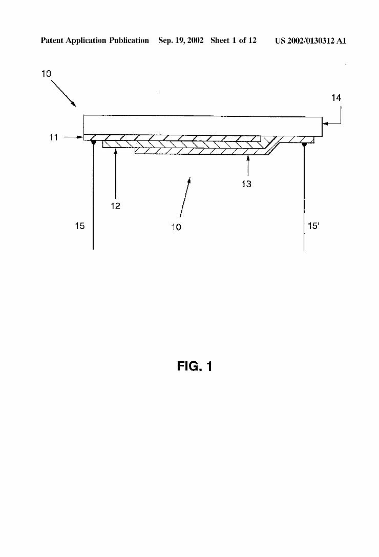
[0019] FIG. 1 is a cross-sectional vieW of a solid state microsWitch (10) made With a semiconducting ?lm (12) sandwiched betWeen tWo conducting electrodes (11, 13) With different or similar Work functions;
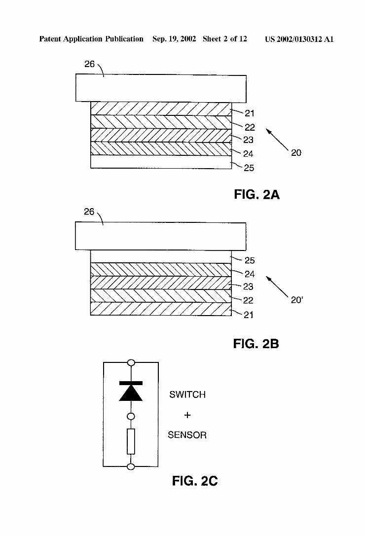
[0020] FIG. 2A is a cross-sectional vieW of a sWitchable tWo-terminal sensing element (20) comprising a microsWitch and a sensing device With electrical properties (such as conductivity, potential difference) Which vary in response to external environment conditions;
[0021] FIG. 2B is a cross-sectional vieW of an alternative structure to that of FIG. 2A in Which the sensor layer 24 is arranged closer to the substrate (26);
[0022] FIG. 2C is a schematic diagram of the equivalent circuit of FIG. 2A and FIG. 2B;
[0023] FIG. 3A shoWs the structure of a column-roW addressable sensor matrix (30) constructed by an array of roW electrodes (35) and an array of column electrodes (31); at each junction betWeen a column and a roW electrode is a sWitchable sensing element similar to that shoWn in FIG. 2;
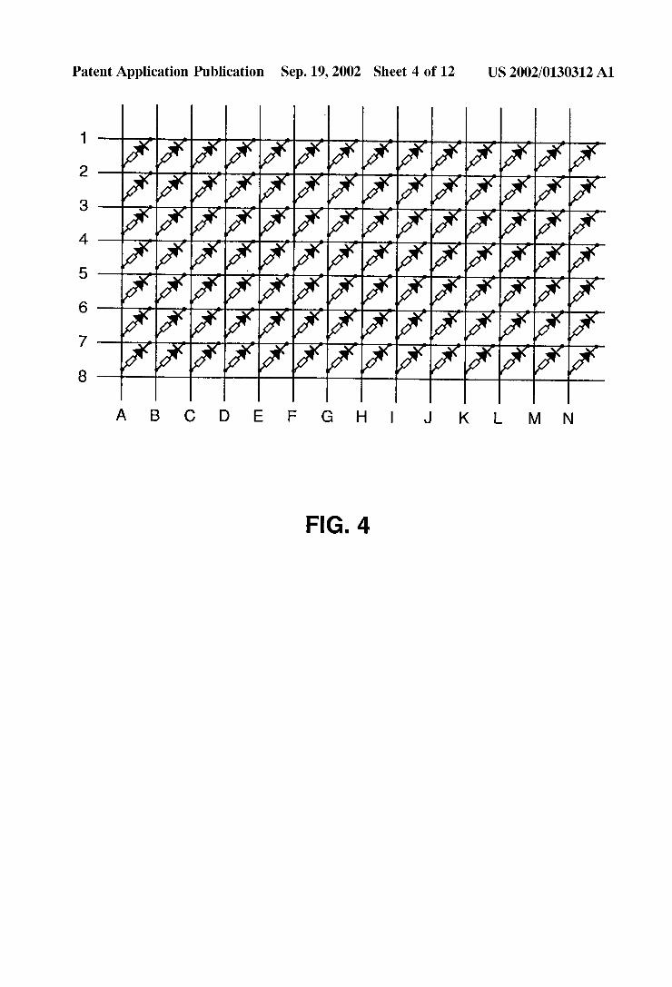
[0024] 3A; [0025] FIG. 4 shoWs the equivalent circuit of an 8x14 sensor matrix;
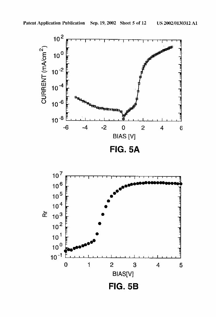
[0026] FIGS. 5A and 5B are a set of graphs Which shoW the I-V characteristics (a) and recti?cation ratio, RI (b) of a microsWitch made in the form of ITO/MEH-PPV/Ca;
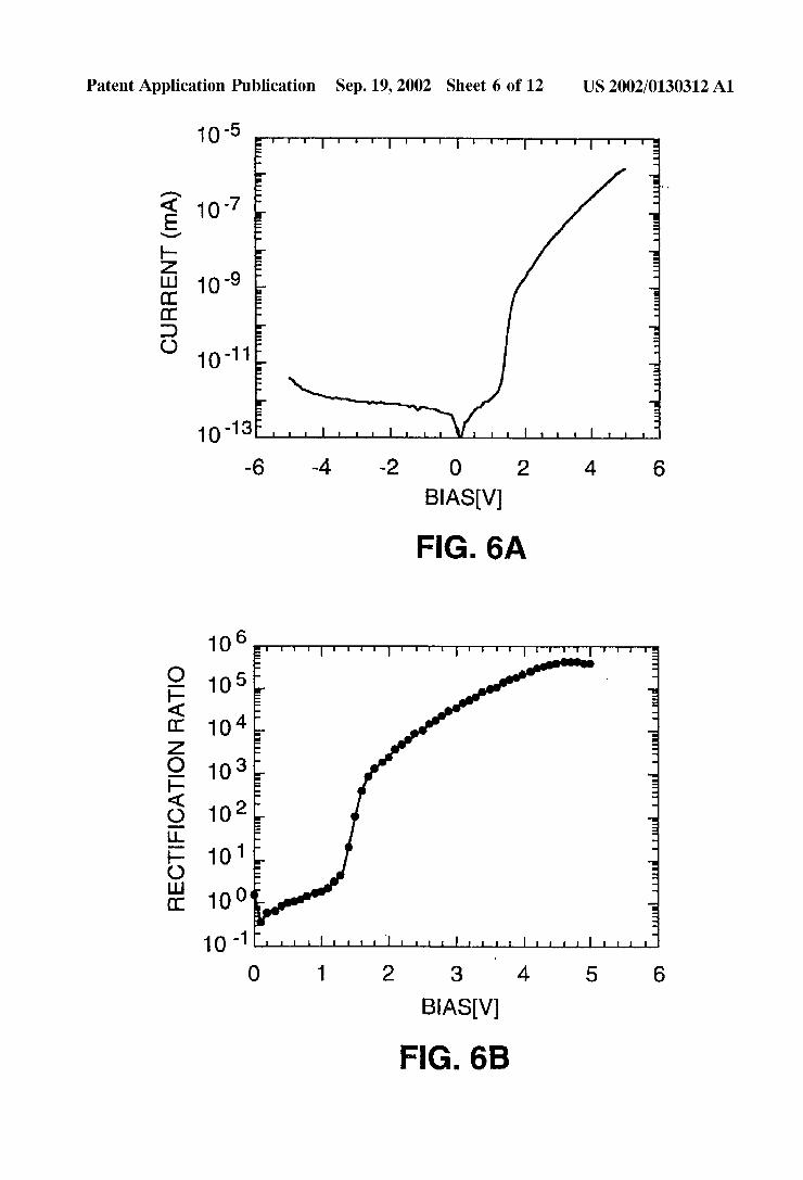
[0027] FIGS. 6A and 6B are a set of graphs Which shoW the I-V characteristics (a) and recti?cation ratio, RI (b) of a microsWitch made in the form of Au/MEHPPV/Al;
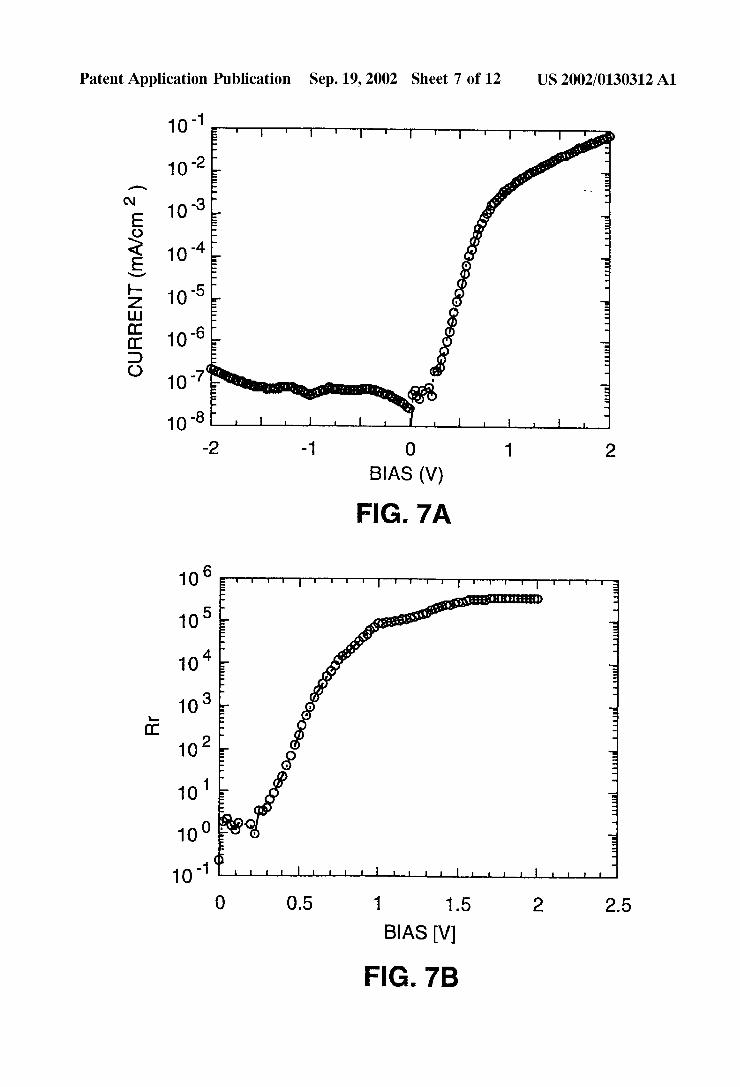
[0028] FIGS. 7A and 7B are a set of graphs Which shoW the I-V characteristics (a) and recti?cation ratio, RI (b) of a microsWitch made in the form of ITO/MEH-PPVzPCBM/Al;
FIG. 3B shoWs the reverse structure to that of FIG.
Sep. 19, 2002
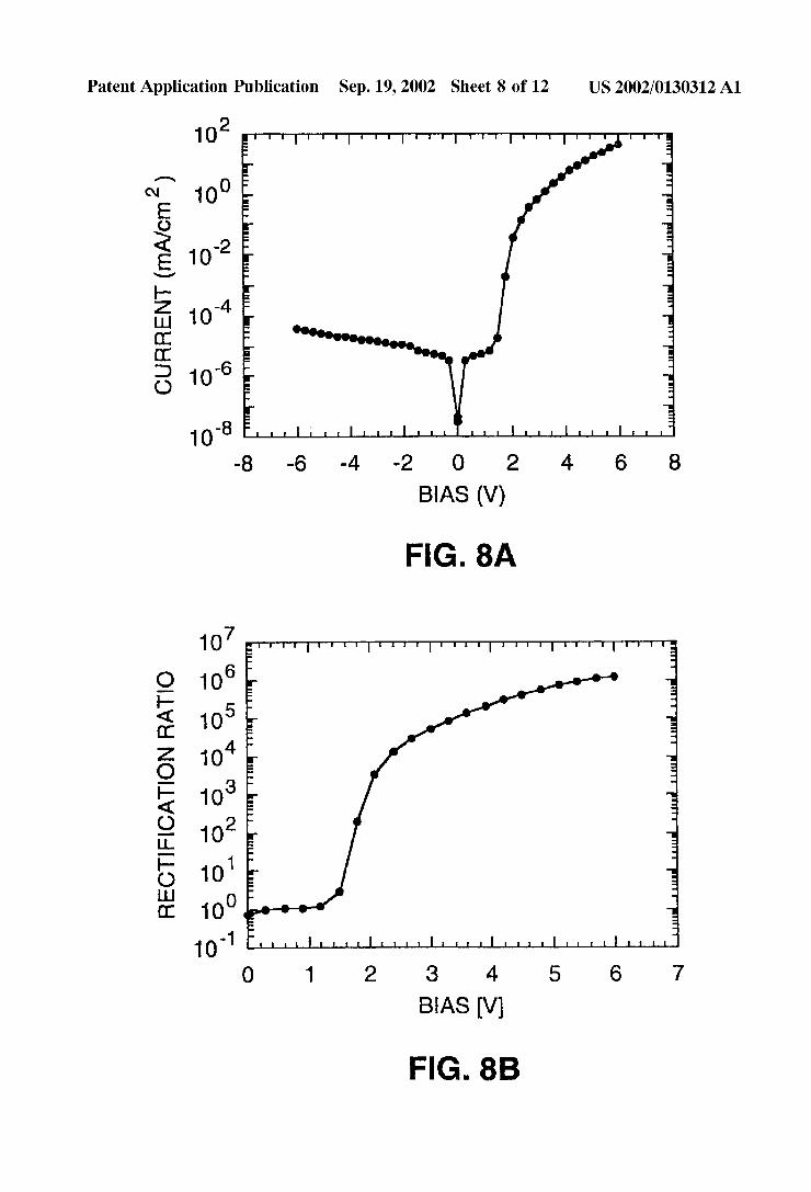
[0029] FIGS. 8A and 8B are a set of graphs Which shoW the I-V characteristics (a) and recti?cation ratio, RI (b) of a microsWitch made in the form of Ag/PANI-PAAMPSA/ MEH-PPV/Ca; [0030] FIGS. 9A and 9B are a set of graphs Which shoW the I-V characteristics (a) and recti?cation ratio, RI (b) of a microsWitch made in the form of ITO/p-i-n/Al in Which the semiconductor Was amorphous silicon ?lm;
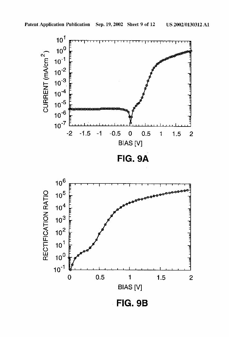
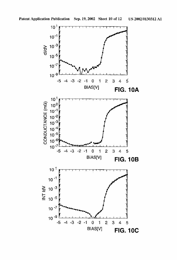
[0031] FIGS. 10A-10C are a set of graphs Which shoW the characteristics of dI/dV-V (a), G-V (b), and current integra tion int IdV-V (c) of a microsWitch made in the form of ITO/MEH-PPV/Ca;
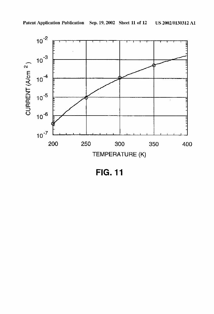
[0032] FIG. 11 shoWs current vs temperature characteris tics of an ITO/MEH-PPV/Ca device in the temperature range betWeen —73° C. and +127° C. (200K to 400K);
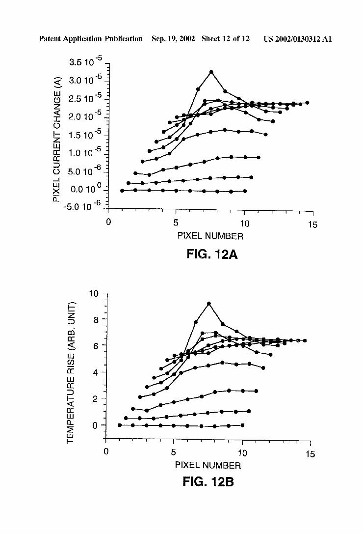
[0033] FIG. 12A and 12B shoW the current image (pixel current distribution) on a 10x10 temperature sensor matrix (a); and the corresponding temperature image from the same matrix
DESCRIPTION OF PREFERRED EMBODIMENTS
[0034] In this description of preferred embodiments and in the claims, reference Will be made to several terms Which must be de?ned. One group of terms concerns the structures of the microsWitches and the sensor elements they can control. Cross-sectional vieWs of tWo embodiments of the microsWitches are shoWn in FIG. 1 and FIG. 2. The sWitch is constructed using the electrode-semiconductor-electrode thin ?lm device con?guration. Speci?cally, the sWitch includes:
[0035] A semiconducting layer (12) comprising organic or inorganic semiconducting material(s). Examples of organic semiconductors include conjugated polymers, polymer blends, polymer/molecule polyblends, layer of organic mol ecules, organometallic molecules, or molecular blends (alloys); or a multilayer structure combining the above materials. Examples of inorganic semiconductors include Si, Se, Ge, Si-Ge alloys, CdS, CdSe, TiO2, CuO, etc. Examples of organic semiconductors include polyacetylene (PA) and its derivatives, polythiophene (PT) and its derivatives, poly(p-phenyl vinylene) (PPV) and its derivatives such as MEH-PPV, fullerene molecules such as C60 and its deriva tives, bucky tubes, anthracene, tetracene, pentacene, Alq3 and other metalchelate (M-L3) type organometallic mol ecules and so on. The layer 12 can also be a composite comprising organic and inorganic materials or in the form of bi-layer or multiple-layers of such materials.
[0036] The layer 12 can be a semiconductor doped With one or more dopants. Extra charges are commonly results from dopants With different valance electrons. A doped semiconductor With electrons as majority charge carriers is called n-type semiconductor and a doped semiconductor With holes as majority carries is called p-type semiconduc tor. The doping levels in the layer 12 can distribute inho mogeneously and can change sign from p-type to n-type (Which forms a p-n junction inside 12) or from p-type to undoped region then to n-doped region (Which forms a p-i-n junction inside 12).
[0037] TWo “contact electrodes” (layers 11, 13) Which serve as the anode and cathode of the sWitches to extract
US 2002/0130312 A1
electrons and holes, respectively, from the semiconductor layer. In some embodiments at least one of the electrodes (e.g., layer 11 in FIG. 1) is made transparent or semitrans parent. These electrodes are described in more detail beloW.
[0038] The anode electrode is de?ned as a conducting material With higher Work function than the cathode mate rial.
[0039] The devices may also include an optional substrate or support 26, as shoWn in FIG. 2A. This is a solid, rigid or ?exible layer designed to provide robustness to the sWitches and/or to the matrix array of sWitches. In some embodiments the substrate is transparent or semitransparent at the Wave lengths of operation. Glass quartZ, polymer sheets, or ?ex ible plastic ?lms are commonly used substrates. Wide band semiconductor Wafers (such as SiC, SiN) can also be used in some applications. In these cases, a thin, doped region can also serve as the contact electrode 21.
[0040] Devices With the “inverted” geometry shoWn in FIG. 2B are also useful In this con?guration, light is incident through the electrode 21 in contact With the free surface; thus, optically opaque materials can be used as substrates. For example, by using an inorganic semiconduc tor Wafer (such as silicon) as the substrate 26, and by doping the semiconductor to “conductive” levels (as de?ned in the folloWing), the Wafer can serve both as the substrate 26 and the contact electrode 25 circuitry built directly onto the inorganic semiconductor substrate (using integrated circuit technology). [0041] Incident light is de?ned generally to include Wave lengths in visible (400-700 nm), Wavelengths in the ultra violet (200-400 nm), Wavelengths in vacuum ultraviolet (<200 nm), and Wavelengths in the near infrared (700-2500 nm). [0042] Several layers are designated as transparent or semi-transparent. These terms are used to refer to the property of a material Which transmits a substantial portion of the incident light incident on it. The term “transparent” is often used to describe a substrate With transmittance over 20% and the term “semitransparent” is often used to describe a substrate or layer With transmittance betWeen 20% and 1%.
[0043] A“conductive” layer or material has a conductivity typically larger than 0.1 S/cm. A semiconducting material has conductivity of from 10'14 to 10'1 S/cm.
[0044] A ‘dielectric’ or an ‘insulating’ layer of material has a conductivity typically loWer than 10-10 S/cm.
[0045] The “positive” (or “negative”) bias refers to situ ations Where a higher potential is applied to the anode electrode (cathode electrode). When values of negative voltage are referred to, as in the case of the reverse bias voltages applied to obtain enhanced photosensitivity, the relative values Will be stated in terms of absolute values; that is, for example, a —10 V (reverse) bias is greater than a —5 V (reverse) bias.
[0046] The spectral response of optical image sensing elements Which one often coupled to its sWitches is deter mined by the optical band gap and the electronic properties (such as carrier mobility) of the sensing material, by the structure of the sensing elements and by the transmission
Sep. 19, 2002
characteristics of the optical ?lters, substrates, or other coating layers in the optical path; as demonstrated in the examples in this application.
[0047] In addition to single band, visible image detection (often referred as black/White, or monochromatic image sensors), there is great demand for image sensors With full-color detectivity. Full-color detection is often achieved by splitting the visible spectrum into three separate regions, the red (600-700 nm), green (500-600 nm) and blue (400 500 nm) fundamental colors. A full-color signal can be represented by the intensities of the incident light in these three bands. A full-color image element thus refers to an image device With three spectral channels in the red, green and blue spectral ranges (sometimes, their complimentary colors, cyan, magenta and yelloW, are chosen), and can provide correct color and light intensity information on the incident light.
[0048] A coating of “black” material (opaque in the spec tral range of interest) in the area betWeen each sensing pixel can be placed in front of the photodetector plane, forming a “black matrix”. This coating is helpful in some situations to further reduce cross-talk betWeen neighbor pixels in devices With an unpatterned photoactive organic layer. Black matri ces have been used in CRT monitors and other ?at panel displays to increase display contrast, and are Well knoWn in the display industry. The patterning of the “black matrix” can be achieved With standard photolithography, stamp, ink-jet or screen printing techniques.
[0049] Electrodes
[0050] In the con?guration shoWn in FIG. 1, a transparent substrate and a transparent electrode are used as one contact electrode. Indium-tin-oxides (“ITO”) can be used as the electrode. Other transparent electrode materials include alu minum doped Zinc oxides (“AZO”), aluminum doped tin oxides (“ATO”), tin-oxides and the like. These conducting coatings are made of doped metal-oxide compounds Which are transparent from near UV to mid-infrared.
[0051] The electrode can also be made With other doped inorganic compounds or alloys. These compounds can be doped into metallic (or near metallic) form by varying the composition of the elements involved, the valance of the elements or the morphology of the ?lms. These semicon ducting or metallic compounds are knoWn in the art and are Well documented (e.g., N. F. Mott, Metal-Insulating Tran sitions, 2nd edition (Taylor & Francis, London, 1990); N. F. Mott and E. A. Davis, Electronic Processes in Non-crystal line Materials (Claredon, Oxford, 1979)]. Examples of such compounds include the cuprate materials Which possess superconductivity at loW temperatures (so-called high tem perature superconductors).
[0052] This electrode can be formed of a conductive polymer such as polyaniline in the emeraldine salt form prepared using the counterion-induced processability tech nology disclosed in Us. Pat. No. 5,232,631 and in Appl. Phys. Lett. 60, 2711 (1992) or other suitable techniques. The polyaniline ?lm Which serves as the electrode can be cast from solution With high uniformity at room temperature. The organic conducting electrodes in combination With polymer substrates and organic active layers alloW these photosen sors be fabricated in fully ?exible form. Other conductive polymers can be used for the transparent or semitransparent
US 2002/0130312 A1
electrode (11 in FIG. 1 or 21 in FIG. 2A) include polyeth ylene dioxythiophene polystyrene sulfonate, (“PEDT/PSS”) [Y Cao, G. Yu, C. Zhang, R. Menon and A. J. Heeger, Synth. Metals, 87, 171 (1997)], poly(pyrrole) or its function deriva tives doped With dodecylbenZene sulfonic acid (“DBSA”) or other acid [J. Gao, A. J. Heeger, J. Y. Lee and C. Y. Kim, Synth. Metals 82, 221 (1996)] and the like.
[0053] A thin semitransparent layer of metals (such as Au, Ag, Al, In etc.) can also be used as electrodes. Typical thicknesses for this semitransparent metal electrode are in the range of 50-1000 A, With optical transmittance betWeen 80% and 1%. Aproper dielectric coating (often in the form of multilayer dielectric stacks) can enhance the transparency in the spectral range of interest [For examples, see S. M. SZe, Physics of Semiconductor Devices (John Wiley & Sons, NeW York, 1981) Chapter 13].
[0054] A transparent electrode can also be made from metal/conducting polymer, conducting polymer/metal/con ducting polymer or dielectric layer/metal/conducting poly mer structures. The transmission properties of these com posite electrodes are improved relative to that of a single metal layer of the same thickness.
[0055] A metal layer With loW optical transmittance can also be used as the electrode for some applications in Which spectral response at certain Wavelengths is of interest. The photosensitivity can be enhanced by fabricating the device in a micro-cavity structure Where the tWo metal electrodes 11 and 13 act also as optical mirrors. Light resonance betWeen the tWo electrodes enhances the photosensitivity at certain Wavelengths and results in selective spectral response, similar to that seen in optical microcavity (optical etalon) devices.
[0056] The “back” electrode 13 in FIG. 1 is typically made of a metal, such as Ca, Sm, Y, Mg, Al, In, Cu, Ag, Au and so on. Metal alloys can also be used as the electrode materials. These metal electrodes can be fabricated by, for example, thermal evaporation, electron beam evaporation, sputtering, chemical vapor deposition, melting process or other technologies. The thickness of the electrode 13 in FIG. 1 (and 11 in FIG. 2) is not critical and can be from hundreds of Angstroms to hundreds of microns or thicker. The thick ness can be controlled to achieve a desired surface conduc tivity.
[0057] When desired, for example, for a photodiode With detectivity on both front and back side, the transparent and semi-transparent materials described above can also be used as the “back” electrode.
[0058] As demonstrated in the examples of this invention, microsWitches With useful I-V characteristics can be fabri cated using contact layers With relatively high resistivity. For example, PANI-PAAMPSA With a bulk resistivity of order 10 Q-cm can be used as the anode material of microsWitches With good sWitching I-V characteristics. For example, in a microsWitch fabricated in the structure of Mg/MEH-PPV/ PANI-PAAMPSA/Ag, the I-V characteristics are de?ned by the Work functions of PANI-PAAMPSA and Mg. Ag serves only a conductor in the test circuit. The advantage of using a contact electrode With high bulk resistivity is that When the lateral resistance is high enough (by proper selection of the bulk resistivity, the thickness of the high resistive anode material and the dimension of the pixels), the cross-talk
Sep. 19, 2002
betWeen pixels becomes suf?ciently small that patterning of the high bulk resistivity material is not necessary.
[0059] TWo “contact electrodes” (11, 13) serve as the anode and cathode of the diodes to inject electrons and holes, respectively, into the semiconducting layer (12). In the devices With undoped semiconductor as layer 12, the anode electrode is de?ned as the one With relatively higher Work function. In the devices With p-n or p-i-n junction in the layer 12, the anode electrode is de?ned as the one in contact With the p-doped region. In all the cases, the anode can be de?ned as the electrode With higher potential When the device is in the conductive mode. In addition to tradi tional metals and alloys, doped semiconductors (both organic and inorganic) can also be used as the contact materials of 11 and 13. An example of using doped silicon as the anode of organic luminescent device has been given by ID. Parker and H. Kim, Appl. Phys. Letters 64, 1774 (1994). Examples demonstrating the utility of conducting polymers such as polyaniline-(camphor sulfonic acid), PAN - ICSA, PEDT-PSS, and polypyrrole, PPy, as electrodes in electroluminescent devices have been disclosed in a number of patents and publications Cao et al., US. Pat. No. 5,232,631; G. Gustafsson, Y. Cao, G. M. Treacy, F. Klavet ter, N. Colaneri and A. J. Heeger, Science 357, 477 (1992); Y Yang, US. Pat. No. 5,723,873; G. HeyWang and F. Jonas, Adv. Materials 4, 116 (1992); Y Cao, G. Yu, C. Zhang, R. Menon and A. J. Heeger, Synth. Metal (1997); J. Gao, A. J. Heeger, J. Y. Lee and C. Y Kim, Synth. Metals 82, 221 (1996)]. [0060] The Semiconductor Layer
[0061] The semiconductor layer is made of a thin sheet of inorganic or organic semiconducting material. Inorganic materials include Si, Se, Ge, CdS, CdSe, Ta0, Cuo, etc. The semiconductor layer can comprise one or more semicon ducting, conjugated polymers, alone or in combination With non-conjugated materials, one or more organic molecules, or oligomers. The semiconducting materials also serve as active layers in the sensor devices to Which these sWitches may be completed. The active organic layer can be a blend of tWo or more conjugated polymers With similar or different electron af?nities and different electronic energy gaps. The active layer can be a blend of tWo or more organic molecules With similar or different electron af?nities and different electronic energy gaps. The active layer can be a blend of conjugated polymers and organic molecules With similar or different electron af?nities and different energy gaps. The latter offers speci?c advantages in that the different electron af?nities of the components can lead to photoinduced charge transfer and charge separation; a phenomenon Which enhances the photosensitivity [N. S. Sariciftci and A. J. Heeger, US. Pat. No. 5,333,183 (Jul. 19, 1994); N. S. Sariciftci and A. J. I-eeger, US. Pat. No. 5,454,880 (Oct. 3, 1995); N. S. Sariciftci, L. SmiloWitZ, A. J. Heeger and F. Wudl, Science 258, 1474 (1992); L. SmiloWitZ, N. S. Sariciftci, R. Wu, C. Gettinger, A. J. Heeger and F. Wudl, Phys. Rev. B 47, 13835 (1993); N. S. Sariciftci and A. J. Heeger, Intern. J. Mod. Phys. B 8, 237 (1994)]. The active layer can also be a series of heterojunctions utiliZing layers of organic materials or blends as indicated above.
[0062] The thin ?lms of organic molecules, oligomers and molecular blends can be fabricated With thermal evapora tion, chemical vapor deposition (CVD) and so on. Thin ?lms
US 2002/0130312 A1
of conjugated polymers, polymer/polymer blends, polymer/ oligomer and polymer/molecule blends can often be fabri cated by casting directly from solution in common solvents or using similar ?uid phase processing. When polymers or polyblends are used as the active layer, the devices can be fabricated onto ?exible substrates yielding unique, mechani cally ?exible photosensors.
[0063] Examples of typical semiconducting conjugated polymers include, but are not limited to, polyacetylene, (“PA”), and its derivatives; polyisothianaphene and its derivatives; polythiophene, (“PT”), and its derivatives; poly pyrrole, (“PPr”), and its derivatives; poly(2,5-thienylenevi nylene), (“PTV”), and its derivatives; poly(pphenylene), (“PPP”), and its derivatives; poly?ourene, (“PF”), and its derivatives; poly(phenylene vinylene), (“PPV”), and its derivatives; polycarbaZole and its derivatives; poly(1,6 heptadiyne); polyisothianaphene and its derivatives; polyquinolene and semiconducting polyanilines (i.e. leucoe meraldine and/or the emeraldine base form). Representative polyaniline materials are described in US. Pat. No. 5,196, 144 Which is incorporated herein by reference. Of these materials, those Which exhibit solubility in organic solvents are preferred because of their processing advantages.
[0064] Examples of PPV derivatives Which are soluble to common organic solvents include poly(2-methoxy-5-(2‘ ethyl-hexyloxy)-1,4-phenylene vinylene), (“MEH-PPV”) [E Wudl, P.-M. Allemand, G. Srdanov, Z. Ni and D. McBranch, in Materials for Nonlinear Optics: Chemical Perspectives, edited by S. R. Marder, J. E. Sohn and G. D. Stucky (The American Chemical Society, Washington DC, 1991), p. 683.], poly(2-butyl-5-(2-ethyl-hexyl)-1,4-phenyle nevinylene), (“BuEHPPV”) [M. A. Andersson, G. Yu, A. J. Heeger, Synth. Metals 85, 1275 (1997)], poly(2,5-bis(c holestanoxy)-1,4-phenylenevinylene), (“BCHA-PPV”) [see US. patent application Ser. No. 07/800,555, incorporated herein by reference] and the like. Examples of soluble PTs include poly(3-alkylthiophenes), (“P3A ”), Wherein the alkyl side chains contain more than 4 carbons, such as from 5 to 30 carbons.
[0065] Organic image sensors can be fabricated using donor/acceptor polyblends as the photoactive layer. These polyblends can be blends of semiconducting polymer/poly mer, or blends of semiconducting polymer With suitable organic molecules and/or organometallic molecules. Examples for the donor of the donor/acceptor polyblends include but are not limited to the conjugated polymers just mentioned, that is PPV, PT, PTV, and poly(phenylene), and their soluble derivatives. Examples for the acceptors of the donor/acceptor polyblends include but are not limited to poly(cyanaophenylenevinylene) (“CN-PPV”), fullerene molecules such as C60 and its functional derivatives, and organic molecules and organometallic molecules used here tofore in the art for photoreceptors or electron transport layers.
[0066] One can also produce photoactive layers using tWo semiconducting organic layers in a donor/acceptor hetero junction (i.e., bilayer) structure or alternation layer struc tures. In these structures, the donor layer is typically a conjugated polymer layer and the acceptor layer is made up of poly(cyanaophenylenevinylene) (“CN-PPV”), fullerene molecules such as C60 and its functional derivatives (such as PCBM and PCBCR), or organic molecules used heretofore
Sep. 19, 2002
in the art for photoreceptors and electron transport layers. Examples of this heterojunction layer structure for a photo active layer include but are not limited to, PPV/C60, MEH PPV/C60, PT/CGO, P3AT/C6O, PTV/C6O and so on.
[0067] The active layer can also be made of Wide band polymers such as poly-N-vinylcarbaZole (“PVK”) doped With dye molecule(s) to enhance the photosensitivity in visible spectral range. In these cases, the Wide band organic serves as both host binder as Well as hole (or electron) transport material. Examples include, but are not limited to, PVK/o-chloranil, PVK/rhodamine B and PVK/coronene and the like.
[0068] The photoactive layer can employ organic mol ecules, oligomers or molecular blends. In this embodiment, the photosensitive material can be fabricated into thin ?lms by chemical vapor deposition, molecular epitaxy or other knoWn ?lm-deposition technologies. Examples of suitable materials include but are not limited to anthracene, phtha locyanine, 6-thiophene (“6T”), 6-phenyl (“6P”), Aluminum chelate (Alq3) and other metal-chelate molecules (m-q3), PBD, spiro-PBD, oxadiaZole and its derivatives or molecu lar blends such as 6T/C6O, 6T/pinacyanol, phthalocyanine/ o-chloranil, 6P/Alq3, 6P/PBD and the like.
[0069] Examples of organic molecules, oligomers and molecular blends can be used for the active layer include anthracene and its derivatives, tetracene and its derivatives, phthalocyanine and its derivatives, pinacyanol and its derivatives, fullerene (“C60”) and its derivatives, thiophene oligomers (such as sixethiophene “6T” and octithiophene “8T”) and their derivatives and the like, phenyl oligomers (such as sixephenyl “6P” or octiphenyl “8P”) and their derivatives and the like, 6T/C6O, 6P/C6O, 6P/Alq3, 6T/pina cyanol, phthalocyanine/o-chloranil, anthracene/C60, anthracene/o-chloranil and the like. For the photoactive layer containing more than tWo types of molecules, the organic layer can be in a blend form, in bilayer form or in multiple alternate layer forms.
[0070] In some embodiments, the active layer 12 com prises one or more organic additives (Which are optically non-active) to modify and to improve the device perfor mance. Examples of the additive molecules include anionic surfactants such as ether sulfates With a common structure,
R(OCH2CH2)nOSO3’M*
[0071] Wherein R represents alkyl alkyllaryl,
[0072] M+ represents proton, metal or ammonium counterion,
[0073] n is moles of ethylene oxide typically n=2 40).
[0074] Application of such anionic surfactants as additives for improving the performance of polymer light-emitting diodes has been demonstrated by Y. Cao [U.S. patent appli cation, Ser. No. 08/888,316, Which is incorporated by ref erence]. [0075] Other types of additives include solid state elec trolytes or organic salts. Examples include poly(ethylene oxide), lithium tri?uoromethanesulfonate, or their blends, tetrabutylammonium dodecylbenZenesulfonate and the like. Application of such electrolyte to luminescent polymers and
US 2002/0130312 A1
invention of neW type of light-emitting devices have been demonstrated in US. Pat. Nos. 5,682,043 and 5,677,546.
[0076] In cases Where the active layer is made of organic blends With tWo or more phases With different electron af?nities and optical energy gaps, nanoscale phase separa tion commonly occurs, and heterojunctions form at the interfacial area. The phase(s) With higher electron af?nity acts as an electron acceptor(s) While the phases With loWer electron af?nity (or loWer ioniZation energy serves as an electron donor(s). These organic blends form a class of charge-transfer materials, and enable the photo-initiated charge separation process de?ned by the folloWing steps [N. S. Sariciftci and A. J. Heeger, Intern. J. Mod. Phys. B 8, 237 (1994)]:
[0077] Step 1: D+A“3>1D*+A, (excitation on D);
[0078] Step 2: 1’3D*+A“1’3(D——A)*, (excitation delocal iZed on D-A complex);
[0079] Step 3: 1’3(D——A)*“1’3(Dd"——Ad_)*, (charge transfer initiated);
[0080] Step 4; 1>3(Dd+--Ad-)*“1>3(D+°--A-°), (ion radical pair formed);
[0082] Where (D) denotes the organic donor and (A) denotes the organic acceptor; 1,3 denote singlet or triplet excited states, respectively.
[0083] Typical thickness of the active layer range from a feW hundred Angstrom units to a feW thousand Angstrom units; i.e., 100-5000A (1 Angstrom unit=10_8cm). Although the active ?lm thicknesses are not critical, device perfor mance can typically be improved by using thinner ?lms With optical densities of less than tWo in the spectral region of interest.
[0084] The microsWitch (10) may also include an optional substrate or support 14, as shoWn in FIG. 1. This is a solid, rigid or ?exible layer designed to provide robustness to the diodes and/or to a matrix array of diodes. Glass, quartZ, polymer sheets or ?exible plastic ?lms are substrates com monly used. Semiconductor Wafers (such as Si, GaAs, SiC, SiN) can also be used as the substrate 14. In these cases, a thin, doped region of the substrate can also serve as the contact electrode 11.
[0085] The current-voltage (I-V) characteristics of the devices shoWn in FIG. 1 are typically asymmetric. As demonstrated in the Examples, the recti?cation ratio (de?ned as the ratio of forWard current to reverse current at a given bias magnitude) can be as high as 106-107; i.e., conductive in the forWard bias direction and insulating at Zero and in reverse bias. Devices With tWo terminals, such as that of FIG. 1, and With strong asymmetry in I-V charac teristics are traditionally called diodes (passive devices) and are represented by a symbol -, in Which the arroW denotes the direction of current ?oW. The sWitching property can be characteriZed by the recti?cation ratio I(V)/I(—V), or the sWitching ratio (a current ratio at tWo given voltages I(V1)/ I(V2) in Which I(V1)>I(V2)). A special situation is V2=0. As demonstrated in the Examples of this invention, the sWitch ing ratio I(V1/I(V2) can be higher than 1010 for V2 close to 0V.
Sep. 19, 2002
[0086] The MSM device (10) shoWn in FIG. 1 can be used as an electric sWitch to sWitch on and off a sensor device in
series With the sWitch, forming a voltage sWitchable sensor unit. TWo geometric structures of the sensor unit 20 are shoWn in FIG. 2A and 2B. This unit 20 includes substrate 26, a sensor made up of electrodes 25 and 23 and sensing element 24. The sWitching function is provided by elec trodes 21 and 23 and semiconductor layer 22. FIG. 2C shoWs their equivalent circuit. Since the conductivity or electric potential (or time derivatives or integrals) of the sensor layer are designed to change in response to external physical conditions (for example, temperature or magnetic ?eld), this sensing circuit can be used as a sensing element Which can be sWitched on in forWard bias and be sWitched off at Zero and reverse bias.
[0087] Many physical effects can be detected by selecting the sensing layer. For example, the resistivity of the sensing layer can change directly in response to changes in the temperature, magnetic ?eld (magnetoresistivity or Hall effect), incident light intensity, incident microWave radiation strength or in response to X-ray or other high energy ?uxes (photoconductive effect) and so on. Alternatively, external environmental changes results in a built-in electric potential in the sensing layer, Which in turn leads to the forWard current change in the circuit unit shoWn in FIG. 2C. Examples include the pieZoelectric effect (voltage change in response to pressure change), the thermoelectric effect (volt age change in response to temperature change), and the photovoltaic effect (voltage change in response to change in incident light intensity), etc. The sensing element (24) shoWn in FIG. 2 can also be used for another type of sensing applications, in Which the derivative and integral of the current vary in response to changes in the external environ ment. As demonstrated in Example 7, the MSM microsWitches shoWn in FIG. 1 also exhibit sWitching characteristics on dI/dV, the integral of I(V), and time derivative and integral of the device current.
[0088] When the sensor (20) is used for light Wave or radio Wave detection, one of the electrodes (25, 21) should be transparent or semitransparent to the incident electromag netic Wave. When the Wave is incident from the substrate side, the substrate needs to be transparent or semitransparent to the incident Wave as Well.
[0089] Column-roW addressable, tWo-dimensional (2D), passive sensor matrices can be constructed With the voltage sWitchable sensor elements, as shoWn in FIG. 2. TWo matrix structures are shoWn in FIG. 3. Their equivalent circuits (in 8 roW, 14 column form) are shoWn in FIG. 4. In these sensor matrices, the electrodes (31, 35) are typically patterned into roWs and columns perpendicular to each other. In the case of FIG. 3A, an array of the column electrodes (31) is ?rst deposited and patterned on the substrate (36). Then, a sensor layer (32) is deposited or cast. When the lateral conduction of the sensor layer betWeen the pixels is suf?ciently loW, this layer does not have to be patterned. Then a metal layer or a doped semiconductor layer (33) is deposited (and patterned, if necessary); (33) serves as the second electrode for each of the sensors, and it serves as the contact electrode to the sWitching diodes. As speci?cally noted, conducting poly mers and other doped semiconductors With proper Work function can be used for layer 33. When the lateral resistance of the material comprising layer 33 is high enough, the cross-talk betWeen neighboring pixels is negligible. In such
US 2002/0130312 A1
cases, 33 need not be patterned, a simpli?cation Which leads to considerable advantage in manufacturing cost and reli ability. The switching layer (34) is then deposited. Finally, the array of the column electrodes (35) is fabricated on top of the sensing layer to complete the column-roW addressable sensor array.
[0090] Patterning of the semiconductor layers (32, 34) is not necessary When the lateral resistance of the material comprising that layer is high enough. Thus, continuous sheets can be used for the sensor matrix. Each cross-point of the roW and column electrodes de?nes a sensing element (pixel) With device structure similar to that shoWn in FIG. 1 or FIG. 2. The roW and the column electrodes also serve as the contact electrodes for the microsWitches and the sensing devices. The electrode 33 can be either a single layer or a bi-layer, to meet the contact needs for both sWitching layer 32 and sensing layer 34. When highly conductive metals are used for 33, this layer needs to be patterned into isolated pixels as that shoWn in FIG. 3. HoWever, a thin layer of metal can be prepared as the electrode 33 in the form of granular particles With a density beloW percolation threshold, the resistance in lateral direc tion is large enough that no patterning of the electrode 33 is necessary. As shoWn in Example 11, such a thin, discon tinuous metal ?lm still provides the Work function needed for the sWitching devices.
[0091] When doped semiconductor layers With relatively high lateral resistivity are used for 33, patterning of 33 can be avoided for certain applications, and a thin continuous coating can be used. The active area of each pixel is de?ned either by the Widths of the roW and column electrodes (31, 35), or de?ned by the patterned siZe of electrode 33, Which ever is smaller.
[0092] The device structure can be reversed so that the sWitching layer is closer to the substrate, as shoWn in FIG. 3B. The preference is dependent on the process simplicity or the type of sensor fabricated. For example, for a pressure sensor Which senses the mechanical pressure near the device pixels, FIG. 3B is the better choice since the sensor layer is closer to the free surface. For an IR sensor in Which an inorganic semiconductor layer (e.g., Ge) is used for IR sensing, the structure of FIG. 3A is favored, since the metal layer (33) can be patterned With conventional photolithog raphy technology on top of the IR sensor (Ge) layer.
[0093] The common electrode 33 provides the Work func tion necessary for the sWitching diodes. Since high resistiv ity polymers (such as PANI) and doped inorganic semicon ductors can provide this function, such materials can be used as the common electrode betWeen the sensing layer and the sWitching layer. In some applications, patterning of the common electrode layer can also be eliminated.
[0094] These microsWitch-based passive sensor matrices can be operated and addressed using schemes similar to those developed for light emitting diode matrices. One practical driving scheme is to apply a positive bias across the roW and column electrode selected (for example, betWeen roW electrode 2 and column electrode B in FIG. 4), leaving the rest ?oating. This is often achieved With analog multi plexers connected to the roW and column electrodes. The pixel at the cross-point of the tWo electrode is then sWitched on With an applied forWard bias larger than the turn-on voltage. Since there is alWays a diode in reverse bias in the
Sep. 19, 2002
parallel paths seen from 2 to B (except the path at the cross-point), the leakage currents from the parallel paths are negligible. Thus, pixel 2B is selected. The current or its integral (charge) or derivative tested in the external test loop connecting 2B is thus sensitive to the physical condition near the pixel 2B. The image of the entire sensor can be electronically recorded by selecting each pixel of the array in time sequence.
[0095] Another driving scheme is achieved by connecting the roW and the column electrodes to digital gates Which provide only tWo possible voltage states, “high” and “loW”. This is often accomplished via digital decoder circuits or digital shift registers. In this driving scheme, three biasing conditions at V+, 0V and V- exist for each sensing pixel. For example, if at an instant of time, roW 2 is selected loW and column B is selected high, then pixel 2B is under forWard bias and is selected. The remainder of the pixels in the roW 2 can be actively turned off by applying the same potential as that of 2 to all the columns except B. These pixels are thus under Zero bias. The remaining pixels in the column B can also be actively turned off by applying the same potential as that of column B to all roWs except 2. In this Way, all the pixels except 2B Will be subject to either Zero bias or reverse bias, and therefore Will not contribute to the current in the external circuit. For the pixels under Zero bias, an even larger sWitching ratio, I(VOn)/I(0V) is achieved than that given by the recti?cation ratio I(VOn)/I(—VOn).
[0096] Another driving scheme is achieved by ?xing all the roW(or column) electrodes at a given potential (such as at 0V) for read out (such as connected to current-voltage converters or current integraters). The column(or roW) elec trodes are scanned one-by-one betWeen the same potential applied to the roW(column) electrodes and the potential corresponding to Von. This operation can be realiZed by a digital shift register or With a digital decoder. In this driving scheme, a column(roW) is sWitched on at a given time, leaving the rest columns(roWs) under Zero bias. The microsWitches connected to the off columns(roWs)are thus in the off state. As shoWn in the Examples, the current sWitch ing ratio I(VOn)/I(0V) can be over 109 times, better than the recti?cation ratio I(VOn)/I(—VOn) Since the data are read out column(roW) by column(roW), the time need for read out the entire matrix can be much faster than that With the point scan schemes.
[0097] There are tWo common approaches to column and roW selections. One is the so-called shift-registration, in Which the pixels are scanned line-by-line in time sequence. This addressing method has been frequently used in emis sive displays made With passive light emitting diodes and in CCD cameras. The other addressing scheme is the so-called “random addressing”, in Which the roW and column elec trodes are encoded and are selectable With a binary decoding circuit. This addressing scheme has frequently been used in memory chips in the computer industry. This scan scheme is interested by its selectability of sensing area With faster frame time. Both addressing schemes can be used to address the microsWitch boards and the integrated sensor matrices shoWn in FIGS. 3 and 4.
[0098] The sWitch matrices disclosed in this invention can be used not only for sensor applications (picking up signals from each pixel location), but also for delivering electric signals (current, charge, voltage and their variations) to