7.2 sepic buck-boost converters - … · circuit; the sepic. 7.2 sepic buck-boost converters ... a...
TRANSCRIPT

5. The length of the trace from GATE output of the HV9930 to the GATE of
the MOSFET should be as small as possible, with the source of the MOSFET
and the GND of the HV9930 being connected to the GND plane. A low
value resistor (10–47 ohms) in series with GATE connection will slow down
the switching edges and greatly reduce EMI, although this will cause
efficiency to decrease slightly. A PNP transistor to discharge the gate quickly
helps to limit the decrease in efficiency, without adding any significant EMI.
6. An R-C damping network might be necessary across diode D1 to reduce
ringing due to the undamped junction capacitance of the diode.
This concludes the Cuk converter design. We can now consider a closely related
circuit; the SEPIC.
7.2 SEPIC Buck-Boost Converters
The abbreviation SEPIC comes from the description Single Ended Primary
Inductance Converter. A SEPIC is a boost-buck converter, like a Cuk, so its input
voltage range can overlap the output voltage. SEPIC circuits can be designed for
constant voltage or constant current output.
The SEPIC topology has been known for some time, but only recently has there
been a revival in its application because: (a) it needs low ESR capacitors and these are
now widely available and (b) it can be used to create AC input power supplies with
power-factor correction that are used to meet worldwide EMI standards.
In automotive and portable applications, batteries are used as a power source for
DC/DC converters. A 12V supply used in automotive applications can have a wide
range of terminal voltage, typically 9V to 16V during normal operation using a lead-
acid battery, but can go as low as 6.5V during cold-crank and as high as 90V during
load-dump (when the battery is disconnected). The peak voltage is usually clamped to
about 40V, using a voltage dependent resistor to absorb the energy.
Lithium batteries have been very successful in portable applications, thanks mostly to
their impressive energy density. A single lithium cell provides an open voltage of 4.2V
when fully charged, and replaces up to three of the alternative NiCd or NiMH cells.
During discharge the cell still retains some energy down to 2.7V. This input voltage
range can be both above and below the output of many DC/DC converters and so
discounts the possibility of using boost or buck converters.
Boost-Buck Converter 131
www.newnespress.com
International standards for power supplies rated above 75W require power-factor
correction (PFC). Having a good power factor means that the current waveform from
the AC line is sinusoidal and in phase with the voltage. Most PFC circuits use a simple
step-up converter as the input stage, implying that the input stage output must exceed
the peak value of the input waveform. In Europe AC inputs of 190–265V RMS are
found, which impose an output of at least 375V, forcing the following converters to
work with elevated input voltages. Typically a PFC input stage has a 400V output.
By using a SEPIC topology, which has a boost-buck topology, the boost section
provides PFC and the buck section produces a lower output voltage. This provides a
compact and efficient design. It provides the required output level even if the peak
input voltage is higher.
7.2.1 Basic SEPIC Equations
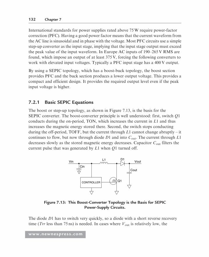
The boost or step-up topology, as shown in Figure 7.13, is the basis for the
SEPIC converter. The boost-converter principle is well understood: first, switch Q1
conducts during the on-period, TON, which increases the current in L1 and thus
increases the magnetic energy stored there. Second, the switch stops conducting
during the off-period, TOFF, but the current through L1 cannot change abruptly – it
continues to flow, but now through diode D1 and into Cout. The current through L1
decreases slowly as the stored magnetic energy decreases. Capacitor Cout filters the
current pulse that was generated by L1 when Q1 turned off.
The diode D1 has to switch very quickly, so a diode with a short reverse recovery
time (Trr less than 75 ns) is needed. In cases where Vout is relatively low, the
Vin
CONTROLLER
L1 D1
Q1
Cout
Vout
Cin
Figure 7.13: This Boost-Converter Topology is the Basis for SEPICPower-Supply Circuits.
132 Chapter 7
www.newnespress.com
efficiency can be improved by using a Schottky diode with low forward voltage
(about 400mV) for D1.
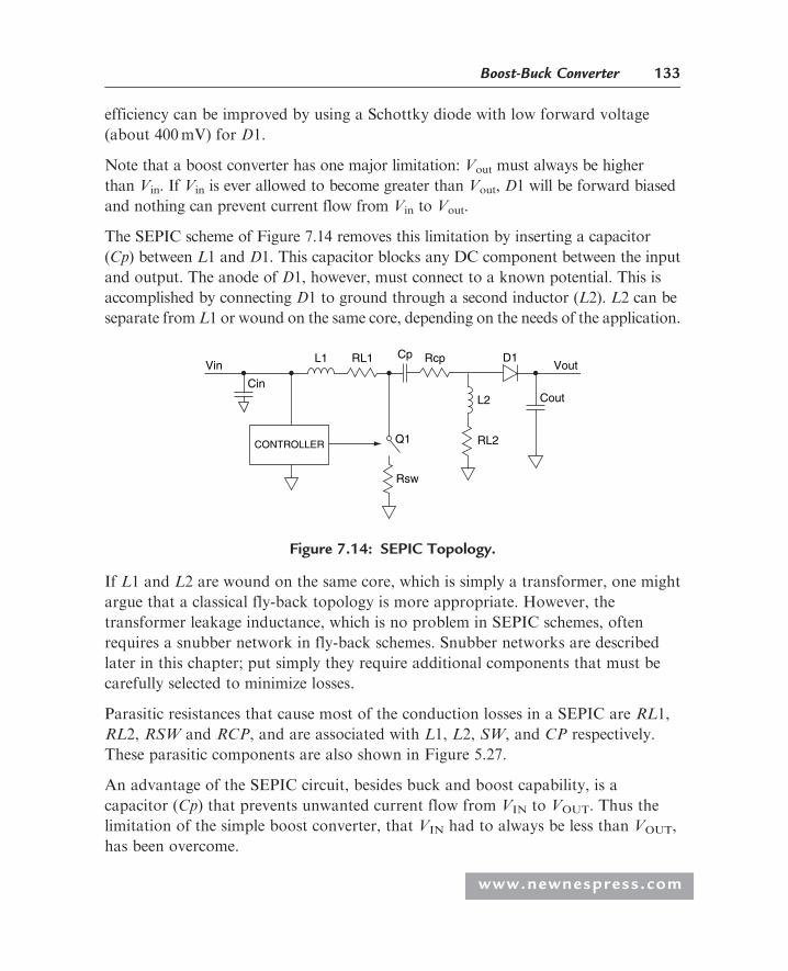
Note that a boost converter has one major limitation: Vout must always be higher
than Vin. If Vin is ever allowed to become greater than Vout, D1 will be forward biased
and nothing can prevent current flow from Vin to Vout.
The SEPIC scheme of Figure 7.14 removes this limitation by inserting a capacitor
(Cp) between L1 and D1. This capacitor blocks any DC component between the input
and output. The anode of D1, however, must connect to a known potential. This is
accomplished by connecting D1 to ground through a second inductor (L2). L2 can be
separate from L1 or wound on the same core, depending on the needs of the application.
If L1 and L2 are wound on the same core, which is simply a transformer, one might
argue that a classical fly-back topology is more appropriate. However, the
transformer leakage inductance, which is no problem in SEPIC schemes, often
requires a snubber network in fly-back schemes. Snubber networks are described
later in this chapter; put simply they require additional components that must be
carefully selected to minimize losses.
Parasitic resistances that cause most of the conduction losses in a SEPIC are RL1,
RL2, RSW and RCP, and are associated with L1, L2, SW, and CP respectively.
These parasitic components are also shown in Figure 5.27.
An advantage of the SEPIC circuit, besides buck and boost capability, is a
capacitor (Cp) that prevents unwanted current flow from VIN to VOUT. Thus the
limitation of the simple boost converter, that VIN had to always be less than VOUT,
has been overcome.
Vin
CONTROLLER
L1 D1RL1 RcpCp
L2
RL2
Rsw
Q1
Cout
Vout
Cin
Figure 7.14: SEPIC Topology.
Boost-Buck Converter 133
www.newnespress.com

Though it has very few elements, the operation of a SEPIC converter is not so
simple to describe by equations; some assumptions have to be made. First, assume
that the values of current and voltage ripple are small with respect to the DC
components. Second, assume that at equilibrium there is no DC voltage across the
two inductances L1 and L2 (neglecting the voltage drop across their parasitic
resistances). By using these assumptions, Cp sees a DC potential of Vin at one
side (through L1) and ground on the other side (through L2). The DC voltage
across Cp is:
VCPðmeanÞ ¼ VIN
The period of one switching cycle is T= 1/frequency. The portion of T for which
switch Q1 is closed is the duty cycle, D, and the remaining part of the period
is thus 1�D. Because the mean voltage across L1 equals zero during steady state
conditions, the voltage seen by L1 during D *T (i.e. the MOSFET ‘ON’ period) is
exactly compensated by the voltage seen by L1 during (1�D) *T (i.e. the MOSFET
‘OFF’ period):
D � T � VIN ¼ 1�Dð Þ � T � ðVOUT þ VD þ VCP � VINÞ
Where VD is the forward voltage drop of D1 for a direct current of (IL1þ IL2), and
VCP is equal to VIN. Simplifying this we get:
D � T � VIN ¼ 1�Dð Þ � T � ðVOUT þ VDÞ
Transposing this, we get:
ðVOUT þ VDÞVIN
¼ D
1�D¼ Ai
Ai is called the amplification factor, where ‘i’ represents the ideal case for which
parasitic resistances are null. Neglecting VD with respect to VOUT (as a first
approximation), we see that the ratio of VOUT to VIN can be greater than or less
than 1, depending on the value of D (with equality obtained for D= 0.5).
134 Chapter 7
www.newnespress.com

The more accurate expression Aa (amplification, actual) accounts for parasitic
resistances in the circuit:
Aa ¼ VOUT þ VD þ IOUT � ðAi � Rcpþ RL2ÞVIN � Ai � IOUT � ðRL1þ RswÞ � Rsw � IOUT
This formula allows computation of the minimum, typical and maximum
amplification factors for Vin (Aamin, Aatyp, and Aamax). The formula is recursive
(‘Aaxxx’ appears in both the result and the expression), but a few iterative
calculations lead to the solution. The expression neglects switching losses due to the
switch Q1 and reverse recovery current in D1. Those losses are usually negligible,
especially if Q1 is a fast MOSFET and its drain-voltage swing (VinþVoutþVd)
remains under 30V.
In some cases, you should also account for losses due to the reverse recovery
current of D1, and for core losses due to high-level swings in stored magnetic energy.
You can extrapolate the corresponding values of D:
D¼Aa=ð1þ AaÞ
Or more generally:
Dxxx¼ Aaxxx=ð1þ AaxxxÞ, where xxx is min, typ or max:
The DC current through Cp is zero, so the mean output current can only be
supplied by L2:
IOUT ¼ IL2
The power-dissipation requirement for L2 is eased, because the mean current into
L2 always equals IOUT and does not depend on variations of VIN.
To calculate the current into L1 (IL1), we can use the fact that no DC current can
flow through Cp. Thus, the coulomb charge flowing during D *T is perfectly
balanced by an opposite coulomb charge during (1�D) *T. When the switch is
closed (for an interval D �T ) the potential at the switch node is fixed at 0V. Since
the capacitor Cp was previously charged to voltage Vin, the anode of D1 will now
Boost-Buck Converter 135
www.newnespress.com
have a potential of �VIN, which reverse-biases D1. Current through Cp is then
IL2. When the switch is open during (1�D) *T, current IL2 flows through D1
while IL1 flows through Cp:
D � T � IL2 ¼ 1�Dð Þ � T � IL1Knowing that IL2 = IOUT,
IL1¼ Aa xxx � IOUT
Input power equals output power divided by efficiency, so IL1 depends strongly on
VIN. For a given output power, IL1 increases if VIN decreases. Knowing that IL2(and hence IOUT) flows into Cp during D*T, we choose Cp so that its ripple delta
Vcp is a very small fraction of Vcp (gamma= 1% to 5%). The worst case occurs when
Vin is minimal.
Cp i IOUT �Dmin � Tgamma � VIN MIN
By using a high switching frequency, small multi-layer ceramic capacitors can be
used for Cp. However, ensure that Cp is able to sustain the power dissipation (Pcp)
due to its own internal equivalent series resistance (Rcp):
Pcp ¼ Aa min � Rcp � IOUT2
The MOSFET switch drain-to-source resistance, in series with a current sense
resistor for limiting the maximum current, is given by the term Rsw. This incurs the
following loss:
Psw ¼ Aa min � ð1þ Aa minÞ � Rsw � IOUT2
Losses PRL1 and PRL2, due to the internal resistances of L1 and L2, are easily
calculated:
PRL1 ¼ Aa min2 � RL1 � IOUT2
PRL2 ¼ RL2 � IOUT2
When calculating the loss due to D1, the average power loss is due to the output
current and the forward voltage drop of D1:
PD1 ¼ VD � IOUT
136 Chapter 7
www.newnespress.com
L1 is chosen so its total current ripple (DIL1) is a fraction (b = 20% to 50%) of IL1.
The worst case for b occurs when VIN is at maximum, because DIL1 is at maximum
when IL1 is at minimum. Assuming b = 0.5:
L1 min ¼ 2 � T � 1�Dmaxð Þ � VIN MAX
IOUT
Choose a standard value nearest to that calculated for L1, and make sure its
saturation current meets the following condition:
IL1 SAT ii IL1 þ 0:5 � DIL1 ¼Aa min �IOUT þ 0:5 � T �Dmin �VIN MIN
L1
The calculation for L2 is similar to that for L1:
L2 min ¼ 2 � T �Dmax � VIN MAX
IOUT
IL2 SAT ii IL2 þ 0:5 � DI2 ¼ IOUT þ 0:5 � T �Dmax � VIN MAX
L2
If L1 and L2 are wound on the same core, you must choose the larger of the two
calculated inductor values. Using a single core, the two windings should be bifilar
(twisted around each other before being wound on the core) and thus will have the
same number of turns and the same inductance values. Otherwise, voltages across
the two windings will differ and Cp will act as a short circuit to the difference. If the
winding voltages are identical, they generate equal and additive current gradients.
In other words, there will be mutual inductance of equal value in both windings.
Thus, the inductance measured across each isolated winding (when there is nothing
connected to the other winding) should equal only half of the value calculated for
L1 and L2.
Because no great potential difference exists between the two windings, you can save
costs by winding them together in the same operation. If the windings’ cross-sections
are equivalent, the resistive losses will differ because their currents (IL1 and IL2) differ.
Total loss, however, is lowest when losses are distributed equally between the two
windings, so it is useful to set each winding’s cross-section according to the current it
carries. This is particularly easy to do when the windings consist of insulated strands
Boost-Buck Converter 137
www.newnespress.com
of wire (Litz) for counteracting the skin effect. Finally, the core size is chosen to
accommodate a saturation current much greater than (IL1þIL2 þ DIL1) at thehighest core temperature anticipated.
The purpose of the output capacitor (COUT) is to average the current pulses
supplied by D1 during TOFF. The capacitor must be able to handle high-level
repetitive surge currents with low ESR and low self-inductance. Fortunately,
ceramic and plastic film capacitors meet these requirements. The minimum value
for COUT is determined by the amount of ripple (DVOUT) that can be tolerated:
COUT �Aa min �IOUT �Dmin �T
DVOUT
The actual value of the output capacitor may need to be much larger than that
calculated using the above equation, especially if the load current is composed of high
energy pulses. The input capacitor can be very small, thanks to the filtering properties
of the SEPIC topology. Usually, CIN can be one tenth the value of COUT:
CIN¼COUT=10
Overall efficiency � can be predicted from VIN and Aa. The result can be
misleading, because it doesn’t account for the switch-transition losses or core
losses and the real efficiency could be much lower:
� ¼ VOUT=AaVIN
Finally, the switch SW and diode D1 should be rated for breakdown voltages with a
15% margin:
VDSðswitchÞ > 1:15ðVOUT þ VD þ VINÞ
VRðdiodeÞ > 1:15ðVOUT þ VINÞ
Example
Let VIN = 50� 150V and VOUT = 15V at 1A maximum. Let us operate at 200 kHz
switching frequency, so that T= 5ms. Now VOUT
VIN¼ D
1�D , so Dmax = 0.231 and
Dmin = 0.091.
L1min ¼ 2Tð1�DmaxÞVIN MAX=IOUT
138 Chapter 7
www.newnespress.com
L1min ¼ 10�5 � 0:769 � 150=1 ¼ 1:15mH, letL1 ¼ 1:5mH
L2min ¼ 2TDmaxVIN MAX=IOUT
L2min ¼ 10�5 � 0:231 � 150=1 ¼ 0:347mH, letL2 ¼ 0:47mH
Cp> IOUT �DminT=ðgamma � VIN MINÞ
Cp > 1 � 0:091 � 2 � 10�5=ð0:05 � 50Þ ¼ 728 nF, let Cp ¼ 1mF:
Now Dxxx¼ Aaxxx=ð1þ AaxxxÞ, where xxx is min, typ or max. So Aamin occurs at
Dmin ¼ 0:091 and Aamin ¼ 0:1:
COUT � Aa min � IOUT �Dmin � T =DVOUT
COUT > 0:1 � 1 � 0:091 � 2 � 10�5=0:1:COUT >> 1:82mF: LetCOUT ¼ 100mF:CIN>COUT=10: LetCIN¼ 10mF:
So, the fundamental component values have been calculated. Now what remains for
the designer is the choice of suitable (and available) parts.
7.3 Buck-Boost Topology
Unlike the boost-buck circuits used by the Cuk and SEPIC topologies, the buck-
boost uses a single inductor. It is a fly-back circuit and hence will be covered in
Chapter 9.
7.4 Common Mistakes in Boost-Buck Circuits
Boost-buck circuits operate with both inductors in continuous conduction mode.
Hence the inductor should be chosen with a value higher than that calculated, to allow
for tolerances and for saturation effects (the inductance falls with increasing current).
Calculate the value, add 20%, and then pick the next highest standard value.
Current ratings of inductors are given for a certain temperature rise in the core,
typically 40�C. So if temperature rise is an issue, pick a component with a higher
current rating.
Boost-Buck Converter 139
www.newnespress.com
7.5 Conclusions
The boost-buck is an ideal topology where the LED load voltage can be higher or
lower than the supply voltage. It should also be used when the supply voltage is no
more than 20% difference (worst case) from the LED load voltage. So if the LED
voltage (maximum) is 20V and the supply voltage (minimum) is 23V, the difference is
3V, and 3/20= 0.15 or 15%, so a Cuk or SEPIC should be used. If the supply voltage
is more than 20% higher, use a buck topology. If the supply voltage is more than
20% lower, use a boost topology. The boost-buck is less efficient compared to buck
or boost topologies.
140 Chapter 7
www.newnespress.com