3d multifunctional integumentary membranes for ...chung3/papers/2014_ncomms.pdf · 3d...
TRANSCRIPT

ARTICLE
Received 9 Nov 2013 | Accepted 27 Jan 2014 | Published 25 Feb 2014
3D multifunctional integumentary membranesfor spatiotemporal cardiac measurements andstimulation across the entire epicardiumLizhi Xu1,*, Sarah R. Gutbrod2,*, Andrew P. Bonifas1, Yewang Su3,4, Matthew S. Sulkin2, Nanshu Lu5,
Hyun-Joong Chung6, Kyung-In Jang1, Zhuangjian Liu7, Ming Ying1, Chi Lu1, R. Chad Webb1, Jong-Seon Kim1,8,
Jacob I. Laughner2, Huanyu Cheng3, Yuhao Liu1, Abid Ameen1, Jae-Woong Jeong1, Gwang-Tae Kim1,
Yonggang Huang3, Igor R. Efimov2 & John A. Rogers1
Means for high-density multiparametric physiological mapping and stimulation are critically
important in both basic and clinical cardiology. Current conformal electronic systems are
essentially 2D sheets, which cannot cover the full epicardial surface or maintain reliable
contact for chronic use without sutures or adhesives. Here we create 3D elastic membranes
shaped precisely to match the epicardium of the heart via the use of 3D printing, as a
platform for deformable arrays of multifunctional sensors, electronic and optoelectronic
components. Such integumentary devices completely envelop the heart, in a form-fitting
manner, and possess inherent elasticity, providing a mechanically stable biotic/abiotic
interface during normal cardiac cycles. Component examples range from actuators for
electrical, thermal and optical stimulation, to sensors for pH, temperature and mechanical
strain. The semiconductor materials include silicon, gallium arsenide and gallium nitride,
co-integrated with metals, metal oxides and polymers, to provide these and other operational
capabilities. Ex vivo physiological experiments demonstrate various functions and methodo-
logical possibilities for cardiac research and therapy.
DOI: 10.1038/ncomms4329
1 Department of Materials Science and Engineering, Frederick Seitz Materials Research Laboratory, University of Illinois at Urbana-Champaign, Urbana, Illinois61801, USA. 2 Department of Biomedical Engineering, Washington University in Saint Louis, Saint Louis, Missouri 63130, USA. 3 Department of Civil andEnvironmental Engineering, Department of Mechanical Engineering, Center for Engineering and Health and Skin Disease Research Center, NorthwesternUniversity, Evanston, Illinois 60208, USA. 4 Center for Mechanics and Materials, Tsinghua University, Beijing 100084, China. 5 Department of AerospaceEngineering and Engineering Mechanics, University of Texas at Austin, Austin, Texas 78712, USA. 6 Department of Chemical and Materials Engineering,University of Alberta, Edmonton, Alberta, Canada T6G 2V4. 7 Institute of High Performance Computing, Agency for Science, Technology and Research,1 Fusionopolis Way, #16-16 Connexis, Singapore 138632, Singapore. 8 Department of Chemical and Biomolecular Engineering (BK21 Program), KoreaAdvanced Institute of Science and Technology, Daejeon 305-701, Republic of Korea. * These authors contributed equally to this work. Correspondence andrequests for materials should be addressed to I.R.E. (email: [email protected]) or to J.A.R. (email: [email protected]).
NATURE COMMUNICATIONS | 5:3329 | DOI: 10.1038/ncomms4329 | www.nature.com/naturecommunications 1
& 2014 Macmillan Publishers Limited. All rights reserved.
Tools for cardiac physiological mapping are indispensablefor the clinical identification and mechanistic under-standing of excitation–contraction coupling, metabolic
dysfunction, arrhythmia and other conditions. Devices developedin the 1980s attempted to address this need by using syntheticfabrics sewn to loosely resemble the shape of the ventricle, withbulk electrodes manually assembled and woven into thisplatform1–4. Although such schemes provide some utility, theydo not enable uniform quality of contact across the heart high-density mapping capabilities, provision for multifunctionalrecordings, precision measurement/stimulation or practicaldeployment as chronic implants. As a result, alternativestrategies based on serial mapping with point-contact cathetersor on imaging techniques that use fluorescence, nuclear magneticresonance or ultrasound have emerged, even though each hassignificant shortcomings5–8.
The ideal scenario remains one in which device functionalityintegrates directly and non-invasively with the heart, suitablefor chronic use. The essential challenge is that the heart is acomplex electromechanical syncytium with numerous elementsworking in synchrony to reliably pump blood and respond tochanging metabolic demands. Although much has been gainedfrom isolated cellular studies, the integral functional behaviouron the organ level and the interaction between the electrical,metabolic and mechanical remodelling in disease states, especiallyin vivo, remain poorly explored due to paucity of adequatetools. Thus, there is an unmet need for multiparametricmapping capabilities inclusive but far beyond electrical sensingin a conformal, high-resolution manner, which cannot berealized using conventional materials, device technologies orimaging modalities.
Recent developments in materials and mechanics concepts forstretchable electronics9–14 create an opportunity to meet thischallenge of direct, full three-dimensional (3D) integration ofdevices with the epicardial surface. Here we expand on previouslyreported small-scale electronic devices as two-dimensional (2D)flexible sheets15, to build multifunctional semiconductor systemsin lithographically defined configurations on 3D, thin elasticmembranes, custom-formed to match the shape of the heart. Thephysical format resembles that of the naturally occurringmembrane that surrounds the heart, known as the pericardium.These systems, which we refer to as 3D multifunctionalintegumentary membranes (3D-MIMs) provide conformalinterfaces to all points on the heart, with robust but non-invasive contacts enabled by the soft elasticity of the membraneitself, throughout dynamic cardiac cycles, even when completelyimmersed in fluid media. Measurements on isolated perfusedrabbit hearts demonstrate the utility of these ideas as a generalplatform for multifunctional, high-density epicardial mapping/stimulation. The results provide advanced methodologicalpossibilities for basic and clinical cardiology.
ResultsDesign and fabrication. The fabrication begins with the creationof a thin, 3D elastic membrane shaped to the heart. As shown inFig. 1a, optical segmentation techniques first capture the full 3Dgeometry of a heart of interest16. A commercial 3D printer(ZPrinter 450, Z-Corporation) then renders a solid model of theheart in a proportionally scaled form, as described later, to serveas a substrate for mounting ultrathin electronic/optoelectronicand sensor systems, separately prefabricated on planar substrates.Casting and curing a thin layer of silicone elastomer on top of theheart model with these multifunctional devices on its surfacedefines the overall format. The front faces of the devicecomponents contact the model while the back faces bond to the
elastomer. Removing the system (that is, 3D membrane withintegrated device components) from the model prepares it forinstallation around a living heart, as a type of ‘instrumented’,artificial pericardium.
Figure 1b shows a representative 3D-MIM that includesmicroscale, inorganic light-emitting diodes (m-ILEDs) based onindium gallium nitride (InGaN) for optical mapping, silicon (Si)nanomembranes for strain gauges, gold (Au) electrodes forelectrical sensing/stimulation, iridium oxide (IrOx) pads for pHsensors and Au serpentine resistors for temperature sensors/heaters. The methods for creating these components exploitmodern integrated circuit technologies and achieve spatialresolution far beyond that possible with manually assembledarrays. A thin, flexible heat-seal conductive cable (Elform, HST-9805-210) serves as a connection to external hardware for dataacquisition, power supply and control. The 3D-MIM isengineered with overall dimensions slightly smaller than thoseof the real heart, to provide adequate elasticity and mechanicalsupport for robust contact with the epicardium during diastoleand systole, but with sufficiently small pressures to avoiddisruption of natural behaviours of the cardiac tissue. Theserpentine mesh that interconnects the device components coversthe ventricle and conforms to the contours of the epicardium.Although this example is designed for research applications onrabbit hearts, the same strategies are applicable to human hearts,or even other organ systems. Here the 3D geometries can beobtained using similar 3D-printed substrates with patient-specificMRI or CT organ segmentation.
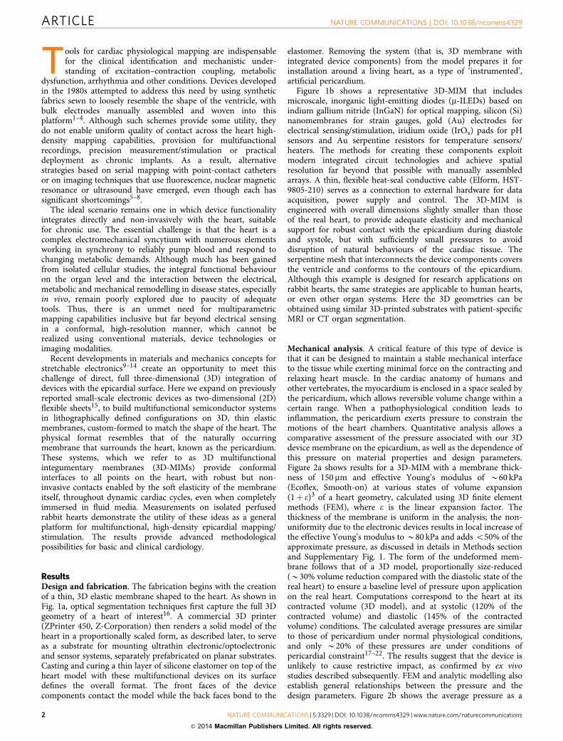
Mechanical analysis. A critical feature of this type of device isthat it can be designed to maintain a stable mechanical interfaceto the tissue while exerting minimal force on the contracting andrelaxing heart muscle. In the cardiac anatomy of humans andother vertebrates, the myocardium is enclosed in a space sealed bythe pericardium, which allows reversible volume change within acertain range. When a pathophysiological condition leads toinflammation, the pericardium exerts pressure to constrain themotions of the heart chambers. Quantitative analysis allows acomparative assessment of the pressure associated with our 3Ddevice membrane on the epicardium, as well as the dependence ofthis pressure on material properties and design parameters.Figure 2a shows results for a 3D-MIM with a membrane thick-ness of 150mm and effective Young’s modulus of B60 kPa(Ecoflex, Smooth-on) at various states of volume expansion(1þ e)3 of a heart geometry, calculated using 3D finite elementmethods (FEM), where e is the linear expansion factor. Thethickness of the membrane is uniform in the analysis; the non-uniformity due to the electronic devices results in local increase ofthe effective Young’s modulus to B80 kPa and adds o50% of theapproximate pressure, as discussed in details in Methods sectionand Supplementary Fig. 1. The form of the undeformed mem-brane follows that of a 3D model, proportionally size-reduced(B30% volume reduction compared with the diastolic state of thereal heart) to ensure a baseline level of pressure upon applicationon the real heart. Computations correspond to the heart at itscontracted volume (3D model), and at systolic (120% of thecontracted volume) and diastolic (145% of the contractedvolume) conditions. The calculated average pressures are similarto those of pericardium under normal physiological conditions,and only B20% of these pressures are under conditions ofpericardial constraint17–22. The results suggest that the device isunlikely to cause restrictive impact, as confirmed by ex vivostudies described subsequently. FEM and analytic modelling alsoestablish general relationships between the pressure and thedesign parameters. Figure 2b shows the average pressure as a
ARTICLE NATURE COMMUNICATIONS | DOI: 10.1038/ncomms4329
2 NATURE COMMUNICATIONS | 5:3329 | DOI: 10.1038/ncomms4329 | www.nature.com/naturecommunications
& 2014 Macmillan Publishers Limited. All rights reserved.

function of the volume expansion, the thickness of the membraneand its Young’s modulus. The analytic model uses a partialellipsoid to approximate the geometry of the heart. Details appearin Methods section and Supplementary Fig. 1. The followingexpression connects the average pressure, the membranegeometry, mechanical properties and expansion factor:
Paverage ¼ C� Ete1� nð Þ 1þ eð Þ2
ð1Þ
where t is the thickness of the membrane, E and n are the effectiveYoung’s modulus and the Poisson’s ratio, respectively. Theconstant C decreases as the heart size increases, and C alsodepends on the shape of the heart (B0.2 mm� 1 for a rabbitheart). Decreases in membrane thicknesses and Young’s moduliboth linearly reduce the pressure. This scaling allows designs thatprovide pressures sufficiently large to maintain good contactbetween the sensor/actuator network and the epicardial surface,but sufficiently small to avoid impact on the intrinsic physiology.Monitoring the time course of several electrophysiologicalparameters that indicate ischaemia in an isolated pressure-loaded, working rabbit heart model23 with and without a
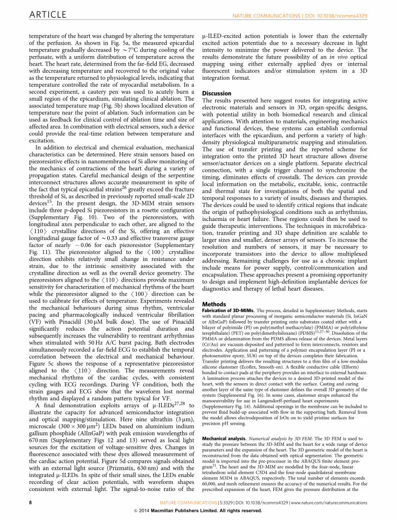
3D-MIM reveals the effects. The results, based on control(N¼ 3) and experimental (N¼ 3) hearts (Supplementary Fig. 2),suggest that there is no additional ischaemia caused by thedevices, as measured by ST elevation and the amplitude of the LVpressure waveform.
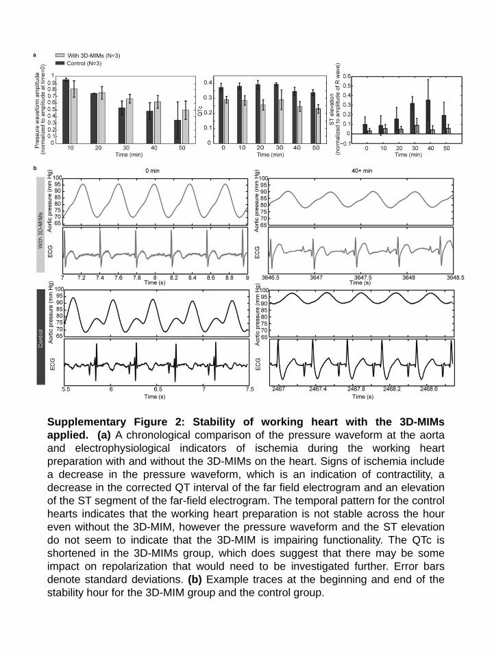
Spatiotemporal cardiac measurements and stimulation. Todemonstrate the various functional modes of operation we beginwith high-precision mapping of epicardial electrical activity.These experiments, and all of those that follow, used explantedLangendorff-perfused rabbit hearts. The 3D geometrical infor-mation was obtained from a representative rabbit heart. A single3D-MIM can accommodate some range in specific sizes andshapes associated with a single type of animal model, due to itssoft, elastic construction. The device here incorporates 68 Auelectrodes (1 mm2 surface area and spacing of 3.5 mm), dis-tributed across both the anterior and posterior surfaces of theepicardium (Fig. 3a,d and Supplementary Fig. 3). The electro-chemical impedances of individual electrodes are B2 kO at afrequency of 1 kHz, measured in phosphate-buffered saline
µ-ILED
Temperature sensor
Si strain gaugeECG sensor
pH sensor
Geometrical information 3D printed model 3D-MIM Integrate with heart
ECG sensor Si strain gauge µ-ILED Temperature sensorpH sensor
Figure 1 | 3D-MIMs for spatiotemporal measurement and stimulation across the entire epicardial surface. (a) Graphical depiction of the key steps in
device design and fabrication. Scale bar, 2 cm. (b) Images of a representative 3D multifunctional integumentary membrane (3D-MIM) integrated on a
Langendorff-perfused rabbit heart. The white arrows highlight various function elements in this system. The electronics can cover both anterior and
posterior surfaces of the heart (inset). Scale bars, 6 mm. (c) Magnified views of the functional elements in conformal contact with the epicardium.
The images are recorded from the back side of the devices. Scale bars, 500mm.
NATURE COMMUNICATIONS | DOI: 10.1038/ncomms4329 ARTICLE
NATURE COMMUNICATIONS | 5:3329 | DOI: 10.1038/ncomms4329 | www.nature.com/naturecommunications 3
& 2014 Macmillan Publishers Limited. All rights reserved.
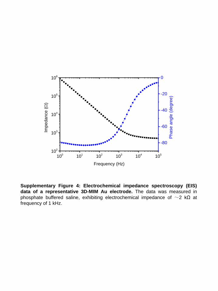
(Supplementary Fig. 4). The transparency of the membraneallows simultaneous optical mapping through voltage-dependentfluorescence, as a means for validating the electrical measure-ments5. Experiments involved signals acquired from four heartsfor a variety of conditions: normal sinus rhythms, and paced at arange of frequencies and from a range of electrode pairs toincrease the variability of the propagation patterns in the spatialactivation maps. The surface electrograms (EGs) captured variouskey morphologies associated with the QRS and T waves (Fig. 3a).Representative maps and correlations between electrical andoptical activation times appear in Fig. 3c,b, respectively. Theoverall linear correlations between optical and electrical activationtimes were 0.957 for sinus data and 0.943 for paced data. Thesestudies indicate that this configuration of measurement electrodescan replicate patterns of activation to a resolution that capturesthe spatial variations observed optically. Analyses for additionalelectrophysiological parameters are summarized inSupplementary Fig. 6. Figure 3d presents a 3D map derivedfrom signals recorded from the anterior and posterior surfaces ofthe heart. Unlike optical mapping where motion artefactsdramatically impact the measurement quality requiring staticheart geometries, electrophysiological mapping with 3D-MIMscan be applied under normal beating condition. As shown inSupplementary Video, the integrated sensors movesynchronously with the underlying cardiac tissue. Although it ispractically difficult to avoid relative lateral motion between thesensors and the epicardium during beating cycles, due to theengineered geometries of 3D-MIMs, the displacement can beminimized to be less than the characteristic sizes of the sensorsand to have negligible impact to the signal quality(Supplementary Fig. 5). This feature is necessary for extendingthe mapping capabilities beyond laboratory studies andimplementing in clinical electrophysiology.
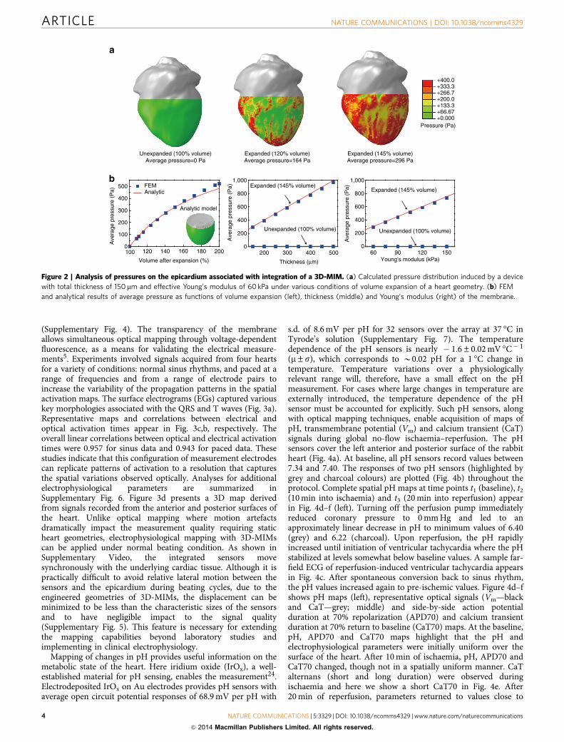
Mapping of changes in pH provides useful information on themetabolic state of the heart. Here iridium oxide (IrOx), a well-established material for pH sensing, enables the measurement24.Electrodeposited IrOx on Au electrodes provides pH sensors withaverage open circuit potential responses of 68.9 mV per pH with
s.d. of 8.6 mV per pH for 32 sensors over the array at 37 �C inTyrode’s solution (Supplementary Fig. 7). The temperaturedependence of the pH sensors is nearly � 1.6±0.02 mV �C� 1
(m±s), which corresponds to B0.02 pH for a 1 �C change intemperature. Temperature variations over a physiologicallyrelevant range will, therefore, have a small effect on the pHmeasurement. For cases where large changes in temperature areexternally introduced, the temperature dependence of the pHsensor must be accounted for explicitly. Such pH sensors, alongwith optical mapping techniques, enable acquisition of maps ofpH, transmembrane potential (Vm) and calcium transient (CaT)signals during global no-flow ischaemia–reperfusion. The pHsensors cover the left anterior and posterior surface of the rabbitheart (Fig. 4a). At baseline, all pH sensors record values between7.34 and 7.40. The responses of two pH sensors (highlighted bygrey and charcoal colours) are plotted (Fig. 4b) throughout theprotocol. Complete spatial pH maps at time points t1 (baseline), t2
(10 min into ischaemia) and t3 (20 min into reperfusion) appearin Fig. 4d–f (left). Turning off the perfusion pump immediatelyreduced coronary pressure to 0 mm Hg and led to anapproximately linear decrease in pH to minimum values of 6.40(grey) and 6.22 (charcoal). Upon reperfusion, the pH rapidlyincreased until initiation of ventricular tachycardia where the pHstabilized at levels somewhat below baseline values. A sample far-field ECG of reperfusion-induced ventricular tachycardia appearsin Fig. 4c. After spontaneous conversion back to sinus rhythm,the pH values increased again to pre-ischemic values. Figure 4d–fshows pH maps (left), representative optical signals (Vm—blackand CaT—grey; middle) and side-by-side action potentialduration at 70% repolarization (APD70) and calcium transientduration at 70% return to baseline (CaT70) maps. At the baseline,pH, APD70 and CaT70 maps highlight that the pH andelectrophysiological parameters were initially uniform over thesurface of the heart. After 10 min of ischaemia, pH, APD70 andCaT70 changed, though not in a spatially uniform manner. CaTalternans (short and long duration) were observed duringischaemia and here we show a short CaT70 in Fig. 4e. After20 min of reperfusion, parameters returned to values close to
Expanded (145% volume)Average pressure=296 Pa
Expanded (120% volume)Average pressure=164 Pa
+400.0+333.3+266.7+200.0+133.3+66.67+0.000
Pressure (Pa)
Volume after expansion (%)
100 120 140 160 180 2000
100
200
300
400
500 FEMAnalytic
400 5000
200
200 300
400
600
800
1,000
Ave
rage
pre
ssur
e (P
a)
Thickness (µm)
60 90 120 1500
200
400
600
800
1,000
Ave
rage
pre
ssur
e (P
a)
Young’s modulus (kPa)
Ave
rage
pre
ssur
e (P
a)
Expanded (145% volume)Expanded (145% volume)
Unexpanded (100% volume) Unexpanded (100% volume)
Unexpanded (100% volume)Average pressure=0 Pa
Analytic model
Figure 2 | Analysis of pressures on the epicardium associated with integration of a 3D-MIM. (a) Calculated pressure distribution induced by a device
with total thickness of 150 mm and effective Young’s modulus of 60 kPa under various conditions of volume expansion of a heart geometry. (b) FEM
and analytical results of average pressure as functions of volume expansion (left), thickness (middle) and Young’s modulus (right) of the membrane.
ARTICLE NATURE COMMUNICATIONS | DOI: 10.1038/ncomms4329
4 NATURE COMMUNICATIONS | 5:3329 | DOI: 10.1038/ncomms4329 | www.nature.com/naturecommunications
& 2014 Macmillan Publishers Limited. All rights reserved.

2
Pacing spikes
0 2 s 0 2 s
0 ms
5
10
15
20
25 ms
0
2
4
6
8
10 ms
Electrode position Optical signalsEpicardial electrograms
Electrode position Optical signalsEpicardial electrograms
0 10 20 30 40 5005
101520253035404550
Optical activation time (ms)
Ele
ctro
gram
act
ivat
ion
time
(ms)
SinusPaced
EGOAPAct time
0 4 8 1612 20
Time (ms)
0
5
10
15
20
25 msAnterior Posterior
1
2 4 5
Nor
mal
ized
vol
tage
/frac
tiona
l flu
ores
cenc
e (a
.u.)
1
2
3
4
5
1) Optical
Electrical
Optical
Electrical2) 3) Optical
Electrical4) Optical
Electrical5) Optical
Electrical
3
Figure 3 | High-density electrical mapping. (a) Representative optical and electrical signals acquired simultaneously from the corresponding numbered
electrode locations on a Langendorff-perfused rabbit heart. Scale bar, 7 mm. (b) Top: schematic illustration of a representative optical action potential,
unipolar EG and position of the activation time, defined as dV@t max
for the optical action potential and � dV@t max
for the EG. Bottom: correlation of electrical and
optical activation times for hearts tested in a variety of states. (c) Interpolated spatial activation maps determined from the electrical and optical
measurements. Top: heart paced by the red pair of electrodes on the membrane. Bottom: sinus rhythm. (d) 3D mapping of electrical signalling from both
the anterior and posterior surfaces of the heart. Interpolated spatial maps of electrical activation time are projected on a representative rabbit heart
geometry, for purposes of visualization. Scale bar, 7 mm.
NATURE COMMUNICATIONS | DOI: 10.1038/ncomms4329 ARTICLE
NATURE COMMUNICATIONS | 5:3329 | DOI: 10.1038/ncomms4329 | www.nature.com/naturecommunications 5
& 2014 Macmillan Publishers Limited. All rights reserved.
the baseline levels. This experiment demonstrates possibilitiesin multiparametric mapping during ischaemia/reperfusion.The information establishes anatomical relationships betweenmetabolism and excitation–contraction coupling.
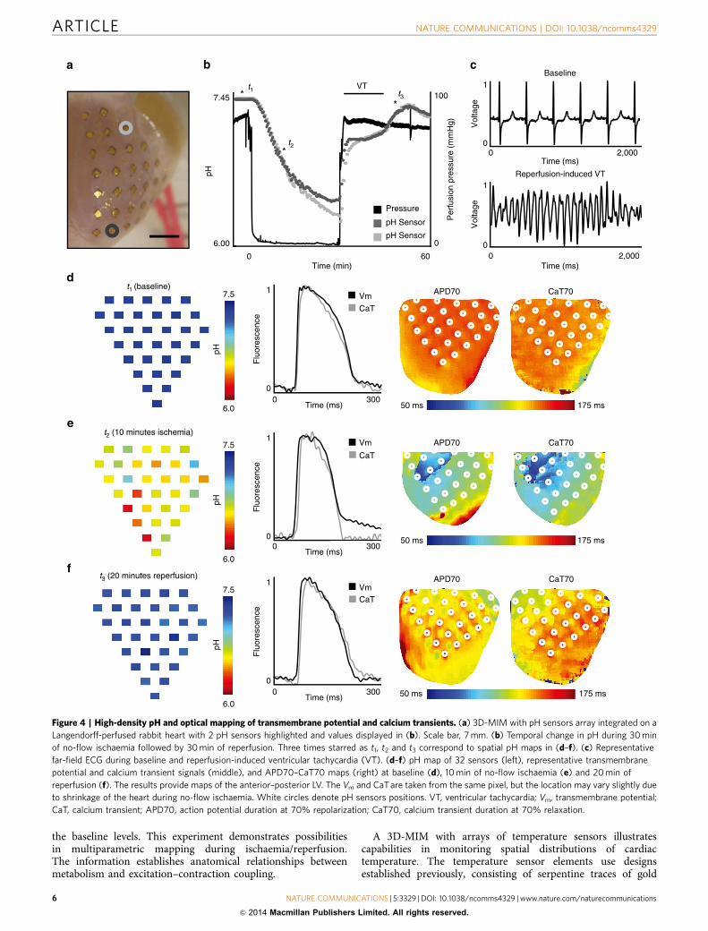
A 3D-MIM with arrays of temperature sensors illustratescapabilities in monitoring spatial distributions of cardiactemperature. The temperature sensor elements use designsestablished previously, consisting of serpentine traces of gold
0
0
pH
Time (min)60
100
Per
fusi
on p
ress
ure
(mm
Hg)
7.45
6.00
VT
Pressure
pH Sensor
pH Sensor
Time (ms)2,0000
Vol
tage
0
1Baseline
Reperfusion-induced VT
Time (ms)2,0000
Vol
tage
0
1
t1*
*
*
t3
t2
7.5
6.0
pH
50 ms 175 ms
APD70 CaT70
Time (ms)0 300
1
0
Vm
CaT
7.5
6.0
pH
50 ms 175 ms
APD70 CaT70Vm
CaT
Time (ms)0 300
1
0
7.5
6.0
pH
50 ms 175 ms
APD70 CaT70VmCaT
Time (ms)0 300
1
0
t3 (20 minutes reperfusion)
t2 (10 minutes ischemia)
t1 (baseline)
Flu
ores
cenc
eF
luor
esce
nce
Flu
ores
cenc
e
Figure 4 | High-density pH and optical mapping of transmembrane potential and calcium transients. (a) 3D-MIM with pH sensors array integrated on a
Langendorff-perfused rabbit heart with 2 pH sensors highlighted and values displayed in (b). Scale bar, 7 mm. (b) Temporal change in pH during 30 min
of no-flow ischaemia followed by 30 min of reperfusion. Three times starred as t1, t2 and t3 correspond to spatial pH maps in (d–f). (c) Representative
far-field ECG during baseline and reperfusion-induced ventricular tachycardia (VT). (d–f) pH map of 32 sensors (left), representative transmembrane
potential and calcium transient signals (middle), and APD70–CaT70 maps (right) at baseline (d), 10 min of no-flow ischaemia (e) and 20 min of
reperfusion (f). The results provide maps of the anterior–posterior LV. The Vm and CaT are taken from the same pixel, but the location may vary slightly due
to shrinkage of the heart during no-flow ischaemia. White circles denote pH sensors positions. VT, ventricular tachycardia; Vm, transmembrane potential;
CaT, calcium transient; APD70, action potential duration at 70% repolarization; CaT70, calcium transient duration at 70% relaxation.
ARTICLE NATURE COMMUNICATIONS | DOI: 10.1038/ncomms4329
6 NATURE COMMUNICATIONS | 5:3329 | DOI: 10.1038/ncomms4329 | www.nature.com/naturecommunications
& 2014 Macmillan Publishers Limited. All rights reserved.
(20 mm wide, 50 nm thick) (Supplementary Fig. 8) in whichchanges in resistance correlate to changes in temperature25. Thetemperature sensors exhibit linear responses over physiologicalrange, with a measurement precision of B23 mK when sampledat 2 Hz in typical hospital settings. Figure 5a shows a 3D-MIM
with 16 integrated temperature sensors during use on a beatingheart. The sensors are calibrated in temperature-controlled waterbath before the animal experiments, exhibiting average responsesof 1.23O �C� 1 with s.d. of 0.05O �C� 1 over 16 sensors acrossthe array (Supplementary Fig. 9). In one experiment, the
30.0
35.0
40.0 °C
Bas
elin
e(1
22 b
.p.m
.)C
old
(71
b.p.
m.)
War
m(1
16 b
.p.m
.)
0 200 400 600 800 1,000
30
32
34
36
38
40
0 5 10 1535
40
45
50
55
60
65
Time (s)
Tem
pera
ture
(°C
)
20
36.0
47.0
58.0°C
0.5%
0.5 1.0 1.5Time (s)
0.5%
0
0.5%
2.0
(R-R0)/R ECG
Sin
us r
hyth
mP
acin
gV
F
Temperature sensors array Time (s)
Tem
pera
ture
(°C
)
Cautery pen
0 200 400 0 200 400Time (ms) Time (ms)
Pacing spike Optical action potential
3D-MIM External
0
1
0
1
Nor
mal
ized
frac
tiona
l flu
ores
cenc
e
0
1
2
3
0
1
2
3
Vol
tage
(V
)
Vol
tage
(V
)
Nor
mal
ized
frac
tiona
l flu
ores
cenc
e
Figure 5 | Temperature and strain sensing combined with imaging enabled by integrated l-ILEDs. (a) Application of a 3D-MIM for temperature
monitoring during cold perfusion. Left: image of a 3D-MIM with 4�4 temperature sensors array integrated on a Langendorff-perfused rabbit heart. Middle:
temperature recordings from a representative sensor illustrated in the left inset. Right: temperature maps at representative time points in the middle inset
with corresponding heart rate calculated from ECG. Each pixel in the colour map corresponds to recording from one temperature sensor. Scale bar, 1 cm.
(b) Temperature measurements during an ablation experiment. Positions of the sensor array and cautery pen are shown in the left inset. Temperature
map during ablation (upper right) and recordings from representative sensors (bottom right) are shown respectively. Scale bar, 7 mm. (c) Responses
of a Si strain sensor under representative physiological conditions, compared with simultaneous ECG recordings. (d) Left: image of a 3D-MIM with m-ILEDs
array in optical mapping experiments. Inset shows a magnified view of area around a representative m-ILED. Right: comparison of optical signals
from a representative pixel (blue dot on the left inset) recorded during excitation using m-ILEDs on 3D-MIM and external optical excitation, respectively.
Scale bar, 3 mm.
NATURE COMMUNICATIONS | DOI: 10.1038/ncomms4329 ARTICLE
NATURE COMMUNICATIONS | 5:3329 | DOI: 10.1038/ncomms4329 | www.nature.com/naturecommunications 7
& 2014 Macmillan Publishers Limited. All rights reserved.
temperature of the heart was changed by altering the temperatureof the perfusion. As shown in Fig. 5a, the measured epicardialtemperature gradually decreased by B7�C during cooling of theperfusate, with a uniform distribution of temperature across theheart. The heart rate, determined from the far-field EG, decreasedwith decreasing temperature and recovered to the original valueas the temperature returned to physiological levels, indicating thattemperature controlled the rate of myocardial metabolism. In asecond experiment, a cautery pen was used to acutely burn asmall region of the epicardium, simulating clinical ablation. Theassociated temperature map (Fig. 5b) shows localized elevation oftemperature near the point of ablation. Such information can beused as feedback for clinical control of ablation time and size ofaffected area. In combination with electrical sensors, such a devicecould provide the real-time relation between temperature andexcitation.
In addition to electrical and chemical evaluation, mechanicalcharacteristics can be determined. Here strain sensors based onpiezoresistive effects in nanomembranes of Si allow monitoring ofthe mechanics of contractions of the heart during a variety ofpropagation states. Careful mechanical design of the serpentineinterconnect structures allows accurate measurement in spite ofthe fact that typical epicardial strains26 greatly exceed the fracturethreshold of Si, as described in previously reported small-scale 2Ddevices15. In the present design, the 3D-MIM strain sensorsinclude three p-doped Si piezoresistors in a rosette configuration(Supplementary Fig. 10). Two of the piezoresistors, withlongitudinal axes perpendicular to each other, are aligned to the/110S crystalline directions of the Si, offering an effectivelongitudinal gauge factor of B0.33 and effective transverse gaugefactor of nearly � 0.06 for each piezoresistor (SupplementaryFig. 11). The piezoresistor aligned to the /100S crystallinedirection exhibits relatively small change in resistance understrain, due to the intrinsic sensitivity associated with thecrystalline direction as well as the overall device geometry. Thepiezoresistors aligned to the /110S directions provide maximumsensitivity for characterization of mechanical rhythms of the heartwhile the piezoresistor aligned to the /100S direction can beused to calibrate for effects of temperature. Experiments revealedthe mechanical behaviours during sinus rhythm, ventricularpacing and pharmacologically induced ventricular fibrillation(VF) with Pinacidil (30mM bulk dose). The use of Pinacidilsignificantly reduces the action potential duration andsubsequently increases the vulnerability to reentrant arrhythmiaswhen stimulated with 50 Hz A/C burst pacing. Bath electrodessimultaneously recorded a far-field ECG to establish the temporalcorrelation between the electrical and mechanical behaviour.Figure 5c shows the response of a representative piezoresistoraligned to the /110S direction. The measurements revealmechanical rhythms of the cardiac cycles, with consistentcycling with ECG recordings. During VF condition, both thestrain gauges and ECG show that the waveform lost normalrhythm and displayed a random pattern typical for VF.
A final demonstration exploits arrays of m-ILEDs27,28 toillustrate the capacity for advanced semiconductor integrationand optical mapping/stimulation. Here nine ultrathin (3 mm),microscale (300� 300 mm2) LEDs based on aluminium indiumgallium phosphide (AlInGaP) with peak emission wavelengths of670 nm (Supplementary Figs 12 and 13) served as local lightsources for the excitation of voltage-sensitive dyes. Changes influorescence associated with these dyes allowed measurement ofthe cardiac action potential. Figure 5d compares signals obtainedwith an external light source (Prizmatix, 630 nm) and with theintegrated m-ILEDs. In spite of their small sizes, the LEDs enablerecording of clear action potentials, with waveform shapesconsistent with external light. The signal-to-noise ratio of the
m-ILED-excited action potentials is lower than the externallyexcited action potentials due to a necessary decrease in lightintensity to minimize the power delivered to the device. Theresults demonstrate the future possibility of an in vivo opticalmapping using either externally applied dyes or internalfluorescent indicators and/or stimulation system in a 3Dintegration format.
DiscussionThe results presented here suggest routes for integrating activeelectronic materials and sensors in 3D, organ-specific designs,with potential utility in both biomedical research and clinicalapplications. With attention to materials, engineering mechanicsand functional devices, these systems can establish conformalinterfaces with the epicardium, and perform a variety of high-density physiological multiparametric mapping and stimulation.The use of transfer printing and the reported scheme forintegration onto the printed 3D heart structure allows diversesensor/actuator devices on a single platform. Separate electricalconnection, with a single trigger channel to synchronize thetiming, eliminates effects of crosstalk. The devices can providelocal information on the metabolic, excitable, ionic, contractileand thermal state for investigations of both the spatial andtemporal responses to a variety of insults, diseases and therapies.The devices could be used to identify critical regions that indicatethe origin of pathophysiological conditions such as arrhythmias,ischaemia or heart failure. These regions could then be used toguide therapeutic interventions. The techniques in microfabrica-tion, transfer printing and 3D shape definition are scalable tolarger sizes and smaller, denser arrays of sensors. To increase theresolution and numbers of sensors, it may be necessary toincorporate transistors into the device to allow multiplexedaddressing. Remaining challenges for use as a chronic implantinclude means for power supply, control/communication andencapsulation. These approaches present a promising opportunityto design and implement high-definition implantable devices fordiagnostics and therapy of lethal heart diseases.
MethodsFabrication of 3D-MIMs. The process, detailed in Supplementary Methods, startswith standard planar processing of inorganic semiconductor materials (Si, InGaNor AlInGaP) followed by transfer printing onto substrates coated either with abilayer of polyimide (PI) on poly(methyl methacrylate) (PMMA) or poly(ethyleneterephthalate) (PET) on poly(dimethylsiloxane) (PDMS)15,27–30. Dissolution of thePMMA or delamination from the PDMS allows release of the devices. Metal layers(Cr/Au) are vacuum-deposited and patterned to form interconnects, resistors andelectrodes. Application and patterning of a polymer encapsulation layer (PI or aphotosensitive epoxy, SU8) on top of the devices completes their fabrication.Transfer printing delivers the resulting structures to a thin film of a low-modulussilicone elastomer (Ecoflex, Smooth-on). A flexible conductive cable (Elform)bonded to contact pads at the periphery provides an interface to external hardware.A lamination process attaches the devices to a desired 3D-printed model of theheart, with the sensors in direct contact with the surface. Casting and curinganother layer of the same type of elastomer defines the overall 3D geometry of thesystem (Supplemental Fig. 16). In some cases, elastomer straps enhanced themanoeuvrability for use in Langendorff-perfused heart experiments(Supplementary Fig. 14). Additional openings in the membrane can be included toprevent fluid build-up associated with flow in the supporting bath. Removal fromthe model allows electrodeposition of IrOx on to yield pristine surfaces forprecision pH sensing.
Mechanical analysis. Numerical analysis by 3D FEM: The 3D FEM is used tostudy the pressure between the 3D-MIM and the heart for a wide range of deviceparameters and the expansion of the heart. The 3D geometric model of the heart isreconstructed from the data obtained with optical segmentation. The geometricmodel is imported into the pre-processor in the ABAQUS finite element pro-gram31. The heart and the 3D-MIM are modelled by the four-node, lineartetrahedron solid element C3D4 and the four-node quadrilateral membraneelement M3D4 in ABAQUS, respectively. The total number of elements exceeds60,000, and mesh refinement ensures the accuracy of the numerical results. For theprescribed expansion of the heart, FEM gives the pressure distribution at the
ARTICLE NATURE COMMUNICATIONS | DOI: 10.1038/ncomms4329
8 NATURE COMMUNICATIONS | 5:3329 | DOI: 10.1038/ncomms4329 | www.nature.com/naturecommunications
& 2014 Macmillan Publishers Limited. All rights reserved.

interface between the 3D-MIM and the heart. The average pressure is thenobtained over the contact area between the 3D-MIM and the heart, that is, theventricles of the heart as in the experiment, as shown in Fig. 2a.
Analytical calculations: The part of the heart that is covered by the 3D-MIM(Fig. 2a) is approximately a partial axisymmetric ellipsoid with the lengths a and bof semi-principal axes, as shown in Supplementary Fig. 1. The 3D-MIM on theheart surface is modelled as a membrane, which deforms from Z2/a2þR2/b2¼ 1when being fabricated on the model to z2/((1þ e)2a2)þ r2/((1þ e)2b2)¼ 1 due tothe linear expansion e of the heart, where (Z, R) and (z,r)¼ ((1þ e)Z, (1þ e)R) areaxial and radial coordinates of the 3D-MIM without and with expansion in theaxisymmatric coordinates, respectively. The plane stress state of the 3D-MIM withbiaxial linear strain e gives the biaxial stress as Ee/(1� v), where E and n are theYoung’s modulus and the Poisson’s ratio of the 3D-MIM, respectively. Themembrane force, accounting for the change of length due to linear expansion, is
T ¼ Ete1� nð Þ 1þ eð Þ ; ð2Þ
where t is the thickness of the 3D-MIM. For a planar curve r¼ r(z), the principalcurvature along the meridional direction is � (dr2/dz2)/(1þ (dr/dz)2)3/2 at anypoint (z, r) on the surface. The other principal curvature along the circumferential
direction is given by rffiffiffiffiffiffiffiffiffiffiffiffiffiffiffiffiffiffiffiffiffiffiffiffiffi1þ dr=dzð Þ2
q. For z¼ (1þ e)Z and r¼ (1þ e)R, the two
principal curvatures are given by
k1 ¼ a4 b1þ eð Þ a4 � a2 X2 þ b2 X2ð Þ3=2
k2 ¼ a2
1þ eð Þbffiffiffiffiffiffiffiffiffiffiffiffiffiffiffiffiffiffiffiffiffiffiffiffiffia4 � a2X2 þ b2X2p
:
(ð3Þ
The pressure on the heart is obtained in terms of the membrane tension andcurvatures as in ref. 32.
P ¼ T k1 þk2ð Þ ð4ÞIts average over the part of Z0rZra (Supplementary Fig. 1a) of the ellipsoidsurface that is in contact with the heart is given by
Paverage ¼R a
Z0P � 2pR
ffiffiffiffiffiffiffiffiffiffiffiffiffiffiffiffiffiffi1þ dR
dZ
� �2q
dZR aZ0
2pRffiffiffiffiffiffiffiffiffiffiffiffiffiffiffiffiffiffi1þ dR
dZ
� �2q
dZ: ð5Þ
This gives Equation (1) in the main text, and
C ¼
R aZ0
a2 a2 þ b2ð Þa2 � a2 � b2ð ÞZ2½ �b a4 � a2 Z2 þ b2Z2ð Þ3=2 R
ffiffiffiffiffiffiffiffiffiffiffiffiffiffiffiffiffiffi1þ dR
dZ
� �2q
dZR aZ0
Rffiffiffiffiffiffiffiffiffiffiffiffiffiffiffiffiffiffi1þ dR
dZ
� �2q
dZð6Þ
For a¼ 15 mm, b¼ 10 mm and X0¼ � 5.5 mm, which best fit the geometric modelof the heart, the average pressure in Equation (1) agrees well with the 3D FEMresults, as shown in Fig. 2b.
The analysis above does not account for the effect of electronic devices on thepressure between the 3D-MIM and heart. Such an effect can be estimated fromEquation (1) by replacing the tensile stiffness Et of the 3D-MIM with the effectivetensile stiffness of the 3D-MIM with the electronic devices. The inset inSupplementary Fig. 1b shows an electronic device on a sheet of the membranematerial (62.8� 24.3� 0.15 mm3), consisting of the interconnects and electrodes.All of the interconnects consist of the Au: 120 nm/Cr: 2 nm composite layersandwiched by 1.2-mm-thick P) layers on each side. The cross section of theelectrodes is similar to that of interconnects but without the top 1.2-mm-thick PIlayer to expose Au. The sheet is modelled by the eight-node solid element C3D8R,and interconnects and electrodes are modelled by the four-node shell element S4Rin ABAQUS, respectively. FEM gives its tensile stiffness to be B1.5 times thatwithout the electronic devices, as shown in Supplementary Fig. 1b.
Animal experiments. Experiments were conducted in accordance with the ethicalguidelines of the National Institutes of Health and with the approval of theInstitutional Animal Care and Use Committee of Washington University inSt Louis. Briefly, the heart is removed via a thoracotomy and a cannula is placed inthe aorta to allow retrograde perfusion of oxygenated Tyrode’s solution. Theperfusion mimics the electrolyte balance within the animal and provides an energysubstrate for the heart to continue to function normally from an electrical per-spective. The heart is submerged in a perfusion chamber maintained at 37 �C witha pH in the range of 7.35–7.45, controlled by oxygen flow. The optical signals oftransmembrane potential (Vm) and calcium transients (CaT) rely on the collectionof fluorescent signals from a potentiometric dye (di-4 ANEPPS or RH-237) orcalcium indicator (Rhod-2) added to the perfusate with a CMOS camera; whenneeded to avoid motion artifacts an excitation–contraction uncoupler (Blebbista-tin) is also added to the perfusate. Supplementary Fig. 15 illustrates representativeexperimental settings.
Data acquisition and processing. Electrophysiology. The electrical signals arerecorded from the Au electrodes on the 3D-MIMs with a 240-channel unipolar EGacquisition system (Astrocard, Boston) and a custom-built interface. Both theoptical and electrical signals are collected at a sampling frequency of 1 kHz, aligned
with a trigger TTL pulse and post-processed separately in custom MATLABsoftware. Post-processing: the electrical signals acquired from the 3D-MIMs arefirst filtered with a 60-Hz notch filter internal to the acquisition software, then theelectrophysiological parameter of interest activation time is calculated (Fig. 3c) andaligned to the spatial coordinates of the electrodes based on the optical backgroundfile. The optical signals are binned, filtered and normalized as previously descri-bed33. A spatial 3� 3 binning filter is applied, as well as a 100-Hz low-pass digitalfilter, and the amplitude of the fractional fluorescence is normalized to between 0and 1 for each pixel’s temporal sequence. The electrophysiological parameters arecalculated for the complete field of view. To create the spatial maps, the activationtimes are interpolated using MATLAB’s internal function for cubic interpolation ofscattered data. The optical map is also sampled at the coordinates of the electrodesand the same interpolation method is applied to compare the full-resolution opticalpattern with the sampled optical map and the electrical map.
pH data. pH data were acquired using measurement of open circuit potential ofeach sensor reference to an Ag/AgCl electrode, using Gamry Reference 600potentiostat. A custom-made relay system was used for multiplexing.
Temperature and strain. Data for temperature and strain sensors are acquiredwith measurements of resistance of each sensor using a custom-built system basedon National Instruments PXI-6289 board. The resistance of each of the 16 sensorsis recorded simultaneously with a 160-mA probe current, a 16-bit A/D converterand a 15-ms sampling period at each sensor.
References1. Harrison, L. et al. The sock electrode array—a tool for determining global
epicardial activation during unstable arrhythmias. Pacing Clin. Electrophysiol.3, 531–540 (1980).
2. Worley, S. J. et al. A new sock electrode for recording epicardial activationfrom the human heart - one size fits all. Pacing Clin. Electrophysiol. 10, 21–31(1987).
3. Farid, T. A. et al. Role of K-ATP channels in the maintenance ofventricular fibrillation in cardiomyopathic human hearts. Circ. Res. 109,1309–1318 (2011).
4. Faris, O. P. et al. Novel technique for cardiac electromechanical mapping withmagnetic resonance imaging tagging and an epicardial electrode sock. Ann.Biomed. Eng. 31, 430–440 (2003).
5. Efimov, I. R., Nikolski, V. P. & Salama, G. Optical imaging of the heart. Circ.Res. 95, 21–33 (2004).
6. Rieke, V. & Pauly, K. B. MR thermometry. J. Magn. Reson. Imaging 27,376–390 (2008).
7. Chan, K. W. Y. et al. MRI-detectable pH nanosensors incorporated intohydrogels for in vivo sensing of transplanted-cell viability. Nat. Mater. 12,268–275 (2013).
8. D’hooge, J. et al. Regional strain and strain rate measurements by cardiacultrasound: principles, implementation and limitations. Eur. J. Echocardiogr.1, 154–170 (2000).
9. Sekitani, T. et al. A rubberlike stretchable active matrix using elasticconductors. Science 321, 1468–1472 (2008).
10. Kaltenbrunner, M. et al. An ultra-lightweight design for imperceptible plasticelectronics. Nature 499, 458–463 (2013).
11. Lipomi, D. J. et al. Skin-like pressure and strain sensors based on transparentelastic films of carbon nanotubes. Nat. Nanotechnol. 6, 788–792 (2011).
12. Yao, H. F., Shum, A. J., Cowan, M., Lahdesmaki, I. & Parviz, B. A. A contactlens with embedded sensor for monitoring tear glucose level. Biosens.Bioelectron. 26, 3290–3296 (2011).
13. Kim, D.-H. et al. Epidermal electronics. Science 333, 838–843 (2011).14. Kim, D.-H. et al. Materials for multifunctional balloon catheters with
capabilities in cardiac electrophysiological mapping and ablation therapy. Nat.Mater. 10, 316–323 (2011).
15. Kim, D. H. et al. Electronic sensor and actuator webs for large-area complexgeometry cardiac mapping and therapy. Proc. Natl Acad. Sci. USA 109,19910–19915 (2012).
16. Lou, Q., Li, W. W. & Efimov, I. R. The role of dynamic instability andwavelength in arrhythmia maintenance as revealed by panoramic imaging withblebbistatin vs. 2,3-butanedione monoxime. Am. J. Physiol. Heart Circ. Physiol.302, H262–H269 (2012).
17. Holt, J. P., Rhode, E. A. & Kines, H. Pericardial and ventricular pressure. Circ.Res. 8, 1171–1181 (1960).
18. Hancock, E. W. Subacute effusive-constrictive pericarditis. Circulation 43, 183(1971).
19. Smiseth, O. A., Frais, M. A., Kingma, I., Smith, E. R. & Tyberg, J. V. Assessmentof pericardial constraint in dogs. Circulation 71, 158–164 (1985).
20. Tyberg, J. V. et al. The relationship between pericardial pressure and right atrialpressure - an intraoperative study. Circulation 73, 428–432 (1986).
NATURE COMMUNICATIONS | DOI: 10.1038/ncomms4329 ARTICLE
NATURE COMMUNICATIONS | 5:3329 | DOI: 10.1038/ncomms4329 | www.nature.com/naturecommunications 9
& 2014 Macmillan Publishers Limited. All rights reserved.

21. deVries, G., Hamilton, D. R., Ter Keurs, H. E. D. J., Beyar, R. & Tyberg, J. V. Anovel technique for measurement of pericardial pressure. Am. J. Physiol. HeartCirc. Physiol. 280, H2815–H2822 (2001).
22. Shabetai, R. Pericardial effusion: haemodynamic spectrum. Heart 90, 255–256(2004).
23. Neely, J. R., Lieberme., H., Battersb., E. j. & Morgan, H. E. Effect of pressuredevelopment on oxygen consumption by isolated rat heart. Am. J. Physiol. 212,804–814 (1967).
24. Chung, H.-J. et al. Stretchable, multiplexed pH sensors with demonstrations onrabbit and human hearts undergoing ischemia. Adv. Healthc. Mater. 3, 59–68.
25. Webb, R. C. et al. Ultrathin conformal devices for precise and continuousthermal characterization of human skin. Nat. Mater. 12, 938–944 (2013).
26. Moore, C. C., Lugo-Olivieri, C. H., McVeigh, E. R. & Zerhouni, E. A.Three-dimensional systolic strain patterns in the normal human left ventricle:characterization with tagged MR imaging. Radiology 214, 453–466 (2000).
27. Kim, R. H. et al. Waterproof AlInGaP optoelectronics on stretchablesubstrates with applications in biomedicine and robotics. Nat. Mater. 9,929–937 (2010).
28. Kim, R. H. et al. Flexible vertical light emitting diodes. Small 8, 3123–3128 (2012).29. Ahn, J. H. et al. Heterogeneous three-dimensional electronics by use of printed
semiconductor nanomaterials. Science 314, 1754–1757 (2006).30. Kim, H. S. et al. Unusual strategies for using indium gallium nitride grown
on silicon (111) for solid-state lighting. Proc. Natl Acad. Sci. USA 108,10072–10077 (2011).
31. Dassault Systemes. Abaqus analysis user’s manual v.6.10 (Dassault SystemesSimulia Corp., 2010).
32. Timoshenko, S. & Woinowsky-Krieger, S. Theory of Plates and Shells (McGraw-Hill, 1959).
33. Laughner, J. I., Ng, F. S., Sulkin, M. S., Arthur, R. M. & Efimov, I. R. Processingand analysis of cardiac optical mapping data obtained with potentiometric dyes.Am. J. Physiol. Heart Circ. Physiol 303, H753–H765 (2012).
AcknowledgementsThis material is based upon work supported by the NIH grants R01 HL115415, R01HL114395 and R21 HL112278, and through the Frederick Seitz Materials ResearchLaboratory and Center for Microanalysis of Materials at the University of Illinois atUrbana-Champaign. L.X. acknowledges support from China Scholarship Council.R.C.W. acknowledges support from the National Science Foundation under grant no.DGE-1144245. H.C. is a Howard Hughes Medical Institute International StudentResearch fellow. We would like to thank Byung-Gik Kim and Hsin-Yun Chao for thehelp on device fabrication and data processing.
Author contributionsL.X., S.R.G., A.P.B., M.S.S., N.L., H.-J.C., I.R.E. and J.A.R. designed the experiments. L.X.,A.P.B., N.L., H.-J.C., K.-I.J., M.Y., C.L., R.C.W., J.-S.K., A.A., J.-W.J., G.-T.K. and J.A.R.carried out the devices fabrication and characterization. L.X., S.R.G., A.P.B., M.S.S., N.L.,H.-J.C, K.-I.J., M.Y., C.L., R.C.W., J.-S.K., J.I.L., Y.L., J.-W.J. and I.R.E carried out theanimal experiments and data analysis. L.X., Y.S., Z.L., H.C., Y.H. and J.A.R. contributedto the mechanical modelling of the system. L.X., S.R.G., Y.S., M.S.S., H.-J.C., Y.H., I.R.E.and J.A.R. co-wrote the paper.
Additional informationSupplementary Information accompanies this paper at http://www.nature.com/naturecommunications
Competing financial interests: The authors declare no competing financial interests.
Reprints and permission information is available online at http://npg.nature.com/reprintsandpermissions/
How to cite this article: Xu, L. et al. 3D multifunctional integumentary membranes forspatiotemporal cardiac measurements and stimulation across the entire epicardium.Nat. Commun. 5:3329 doi: 10.1038/ncomms4329 (2014).
ARTICLE NATURE COMMUNICATIONS | DOI: 10.1038/ncomms4329
10 NATURE COMMUNICATIONS | 5:3329 | DOI: 10.1038/ncomms4329 | www.nature.com/naturecommunications
& 2014 Macmillan Publishers Limited. All rights reserved.

a
2 2
2 21
Z R
a b
b
0 2 4 6 8 100.0
3.0k
6.0k
9.0k0.0
3.0k
6.0k
9.0k
apparent
apparent
,apparent apparent
With electronic devices
Without electronic devices
With electronic devices
Without electronic devices
100%apparent
0Z,Z z
,R r
1 a
2 2
2 22 21
1 1
z r
a b
1 b
b
aO
Supplementary Figure 1: Mechanical analysis of the devices. (a) Schematic
illustration of the partial axisymmetric ellipsoid with the lengths a and b of semi-
principal axes for the analytic model. (b) The comparison of the stiffness of the
3D-MIM with and without electronic devices along two directions.
With expansion
Without expansion
Heart
Supplementary Figure 2: Stability of working heart with the 3D-MIMs
applied. (a) A chronological comparison of the pressure waveform at the aorta
and electrophysiological indicators of ischemia during the working heart
preparation with and without the 3D-MIMs on the heart. Signs of ischemia include
a decrease in the pressure waveform, which is an indication of contractility, a
decrease in the corrected QT interval of the far field electrogram and an elevation
of the ST segment of the far-field electrogram. The temporal pattern for the control
hearts indicates that the working heart preparation is not stable across the hour
even without the 3D-MIM, however the pressure waveform and the ST elevation
do not seem to indicate that the 3D-MIM is impairing functionality. The QTc is
shortened in the 3D-MIMs group, which does suggest that there may be some
impact on repolarization that would need to be investigated further. Error bars
denote standard deviations. (b) Example traces at the beginning and end of the
stability hour for the 3D-MIM group and the control group.

Cable connection
31 mm
18.5
mm
Electrode
Interconnects
Supplementary Figure 3: Design of the electrodes array for high precision
ECG and pH mappings. The insets show magnified image of the Au electrode,
electrode with electrodeposited IrOx, and interconnects with PI base and
encapsulation layers, respectively.
PI base and
encapsulation
Interconnects
100 μm
600 μm 600 μm
Au electrode Electrode with
electrodeposited IrOx
Supplementary Figure 4: Electrochemical impedance spectroscopy (EIS)
data of a representative 3D-MIM Au electrode. The data was measured in
phosphate buffered saline, exhibiting electrochemical impedance of ~2 kΩ at
frequency of 1 kHz.
100
101
102
103
104
105
102
103
104
105
106
Frequency (Hz)
Imp
ed
an
ce
(
)
-80
-60
-40
-20
0
Ph
ase
an
gle
(d
eg
ree
)
Supplementary Figure 5: Comparison of signal quality of 3D-MIMs
electrophysiological measurements under beating and arrested heart
conditions. Surface electrogram recordings under both beating (a) and arrested
(b) conditions capture various morphologies of the QRS and T waves. (c)
Comparison of the signal to noise ratio (SNR) of the measurements. Error bars
denote standard deviations.

Supplementary Figure 6: Demonstration of spatial mapping of repolarization
parameters with 3D-MIMs. (a) Representative electrical trace from the device
overlaid with a corresponding optical trace for validation defines activation
recovery interval (ARI) from max -dV/dt to the max dV/dt after the QRS complex
and defines action potential duration to 80% repolarization (APD80) from max
dV/dt to 80% recovery. (b) Correlation between the activation recovery interval
from the electrograms and the corresponding optical action potential duration from
a variety of conditions. (c) Representative spatial reconstruction of repolarization
parameters with the electrical device and the optical mapping.
Norm
aliz
ed v
oltage (
a.u
.)
Norm
aliz
ed f
ractional fluore
scence (
a.u
.)
a b
c
5.5 6.0 6.5 7.0 7.5
100
200
300
400
OC
P [m
V]
pH (Glass Electrode)
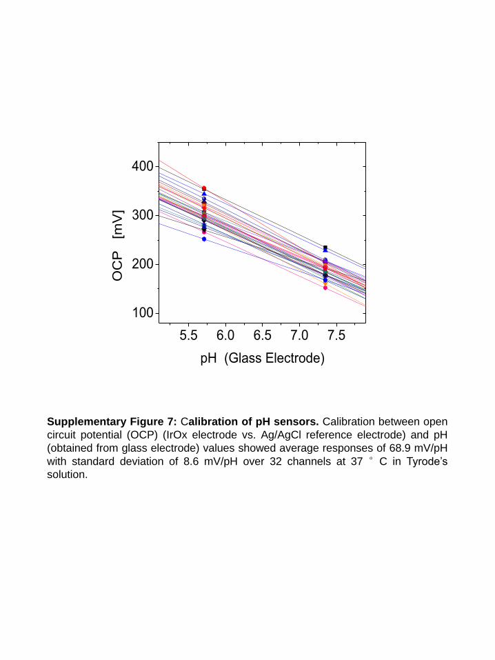
Supplementary Figure 7: Calibration of pH sensors. Calibration between open
circuit potential (OCP) (IrOx electrode vs. Ag/AgCl reference electrode) and pH
(obtained from glass electrode) values showed average responses of 68.9 mV/pH
with standard deviation of 8.6 mV/pH over 32 channels at 37 °C in Tyrode’s
solution.

Supplementary Figure 8: Design of the temperature sensors array. The inset
shows the magnified view of a Au serpentine trace for temperature sensing.
15 mm
11 m
m
Temperature sensor
300 μm
Interconnects
Cable connection

15 20 25 30 35 40 45 50 55 60 65
840
860
880
900
920
940
960
R
esis
tan
ce
(
)
Temperature (°C)
Supplementary Figure 9: Calibration of the temperature sensors. Calibration
is performed by submerging the 3D-MIM with 16 temperature sensors array into
a digital circulating water bath (Fisher Scientific 15-474-100). The resistance is
measured with a custom built system based on National Instruments PXI-6289
board and the temperature is controlled and monitored through the water bath.
Linear fit is applied to each sensor to obtain the relationship between resistance
and temperature.

Supplementary Figure 10: Si strain sensors array. (a) Design and optical
microscope image of the Si strain sensors array. Inset: optical microscope image
of 3 p-doped Si piezoresistors arranged in a rosette configuration. Longitudinal
axes of piezoresistor 1 and 3 correspond to <110> crystalline directions,
longintudinal axis of piezoresistor 2 corresponds to <100> direction. (b) Image of
a 3D-MIM with Si strain sensors array integrated on a Langendorff-perfused rabbit
heart.
16 mm
11 m
m
RV LV
a
b
8 mm
Si strain sensors
Interconnects
Cable connection

Supplementary Figure 11: Tensile test of the Si strain sensors. Fractional
resistance changes of the 3 Si piezoresistors showed in Supplementary Fig. 10,
as functions of uniaxial tensile strain applied in direction parallel to the longitudinal
axis of piezoresistor 1. The calculated effective longitudinal gauge factor is 0.33,
and effective transverse gauge factor is ~-0.06, for piezoresistors aligned to
<110> directions (1 and 3).
0 6 12 15 9 -1
3
0
1
2
3
6
5
4
Strain (%)
(R-R
0 )
/R0 (%
)
1 2 3

7.7 mm
7.7
mm
Interconnects
Cable connection
μ-ILED
Supplementary Figure 12: Design of the μ-ILEDs array for optical mapping
experiments..
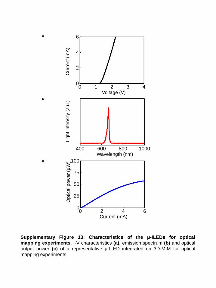
0 2 4 60
25
50
75
100
400 600 800 1000
0 1 2 3 40
2
4
6
Voltage (V)
Curr
ent (m
A)
Wavelength (nm)
Lig
ht in
tensity (
a.u
.) b
a
c
Current (mA)
Optical pow
er
(μW
)
Supplementary Figure 13: Characteristics of the μ-ILEDs for optical
mapping experiments. I-V characteristics (a), emission spectrum (b) and optical
output power (c) of a representative μ-ILED integrated on 3D-MIM for optical
mapping experiments.

Supplementary Figure 14: Fixtures for maneuvering the 3D-MIM for
Langendorff-perfused rabbit heart experiments. 6 silicone straps were
integrated into the 3D-MIM to provide support and control of the opening of the
device. Each strap is attached to a custom made fixture for independent control.
Elastomer straps
Tissue chamber
A Langendorff-perfused
rabbit heart with a 3D-MIM
Conductive cable Custom made fixture

Supplementary Figure 15: Experimental setup for Langendorff-perfused
rabbit heart experiments and optical mapping.
CMOS camera
Tissue chamber
Perfusion system
A Langendorff--perfused
rabbit heart with a 3D-MIM
External light source
CMOS camera
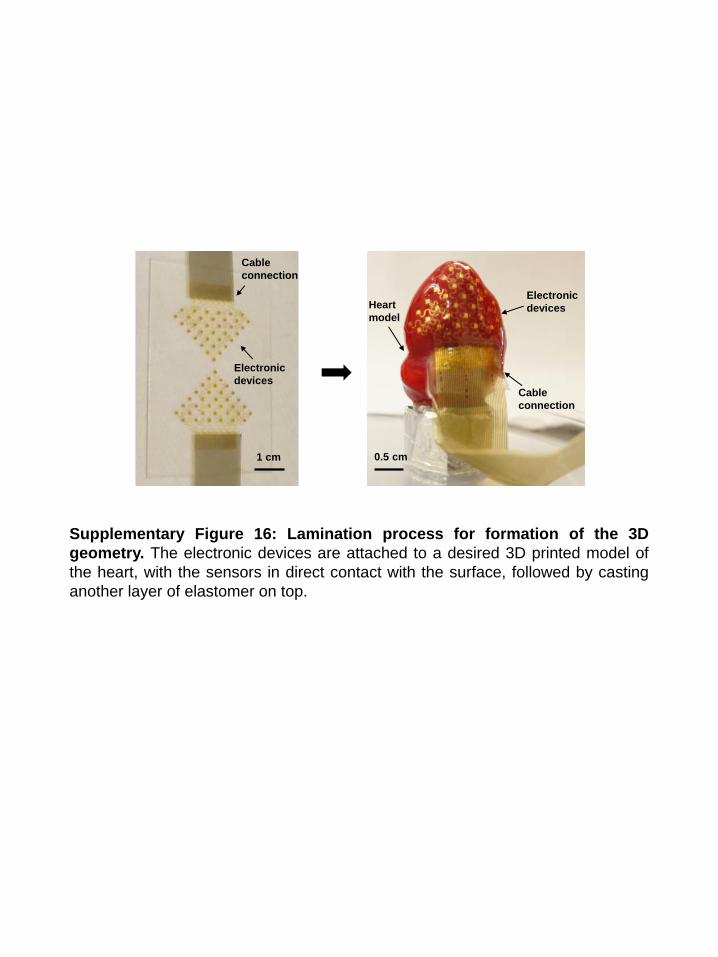
Heart
model
Electronic
devices
Cable
connection
Supplementary Figure 16: Lamination process for formation of the 3D
geometry. The electronic devices are attached to a desired 3D printed model of
the heart, with the sensors in direct contact with the surface, followed by casting
another layer of elastomer on top.
1 cm 0.5 cm
Electronic
devices
Cable
connection

1
Supplementary Methods: Fabrication procedures for 3D-MIMs
I. 3D-MIM with various electronics components array appeared in Fig. 1.
p-doping of Si nanomembrane.
1. Clean a silicon on insulator (SOI) wafer (320 nm Si on 150 nm buried oxide) with
acetone, isopropyl alcohol (IPA) and deionized (DI) water, dehydrate at 110°C for 5
min.
2. Clean with buffer oxide etch (BOE) 6:1 for 1 min.
3. Expose to diffusive boron source at 1,000 °C for 10 min.
4. Clean the processed wafer with HF for 1 min, RCA 1 for 10 min, RCA 2 for 10 min,
and BOE for 1 min.
Preparation of InGaN μ-ILEDs (Ref. 30).
5. Spin coating and patterning of photoresist (PR) (AZ 5214 E), for n-contact, on a
GaN/Si (111) epi-wafer (Azzurro Semiconductor, GaN: Mg (110 nm)//five repeats
of InGaN (3 nm), GaN: Si (10 nm)//GaN: Si (1,700 nm)//AlN: Si/GaN: Si (1,900
nm)//GaN (750 nm)//AlN/AlGaN (300 nm)//Si (111)).
6. Inductively coupled plasma reactive ion etching (ICP-RIE): (a). 3 mTorr, 15 sccm of
BCl3, with RF power of 300 W and parallel plate DC voltage of 100 V for 90 s, then
(b). 3 mTorr, 15 sccm of Cl2, with RF power of 300 W and parallel plate DC voltage
of 100 V for 120 s.
7. Remove native oxide with BOE 10:1 for 120 s.

2
8. Deposit Ti: 15 nm/Al: 60 nm/Mo: 20 nm/Au: 100 nm with e-beam evaporator.
9. Lift-off (ultrasonic with acetone for 120s).
10. Annealing at 860 °C for 30 s in N2 ambient.
11. PR patterning for p-spreading layer.
12. Immerse in HCl∶DI=3∶1 for 5 min
13. Deposit Ni: 10 nm/Au: 10 nm via e-beam evaporator.
14. Lift-off.
15. Annealing at 500 °C for 10 min in air ambient.
16. PR patterning for p-contact pad.
17. Deposit Ti: 10 nm/Au: 120 nm via e-beam evaporator.
18. Lift-off.
19. Deposit Si3N4:300 nm via plasma enhanced chemical vapor deposition (PECVD).
20. PR patterning for anchors.
21. Deposit Ti: 50 nm/Ni: 450 nm via e-beam evaporator.
22. Lift-off.
23. Etching for Si3N4 mask with reactive ion etching (RIE) (SF6 40 sccm, pressure 35
mTorr, and RF power 100 W, etch time >3min).
24. Etching of Si3N4 and GaN/InGaN/AlN/AlGaN epi-layers with ICP-RIE: (a). 5
mTorr, 25 °C, 10 sccm of BCl3, 16 sccm of Cl2, 4 sccm of Ar, 500 W, 300 V, 1 min
(b). 5 mTorr, 25 °C, 20 sccm of Cl2, sccm of Ar, 500 W, 260 V, 8 min.
25. Immerse in KOH (PSE-200, Transene) with 100 °C for 45 min (100*100 μm), for

3
anisotropic undercut of Si.
26. Ni etching (Transene TFB) for ~200 s (etch rate 3nm/s at room temp).
27. Etching of Si3N4 with RIE.
PET base layer preparation.
28. Spin cast poly(dimethylsiloxane) (PDMS) (Sylgard 184, Dow Corning) on glass
slide (3,000 rpm, 30 s).
29. Cure PDMS at 70 °C for 2 hours.
30. Laminate poly(ethylene terephthalate) (PET) film with thickness of 2.5μm on the
surface of PDMS.
Transfer printing of Si nanomembrane onto PET base layer.
31. Pattern PR (S1805, Microposit) with 3 µm pitch dot patterns.
32. Etch silicon by RIE (50mTorr, 40sccm SF6, 100W, 1 min).
33. Undercut buried oxide layer of SOI wafer via dot patterns in HF for 30 min.
34. Spin coat SU-8 2 epoxy (Microchem) on the PET film (3,000 rpm, 30 s).
35. Bake at 65 °C for 30s.
36. Pick up Si nanomembrane with PDMS stamp from SOI wafer.
37. Print Si layer onto SU-8 layer.
38. Cure SU-8 layer with ultraviolet (UV) light exposure from the back side of the glass
slide.
39. Bake at 95 °C for 30s and remove the stamp.
40. Bake at 150 °C for 15 min.

4
41. Strip PR with acetone, IPA and DI water.
Si Patterning.
42. Patterning of PR (S1805).
43. Etch silicon by RIE (50 mTorr, 40 sccm SF6, 100 W, 1 min).
44. Strip PR with acetone, IPA and DI water.
1st Metallization.
45. Deposit Cr: 10 nm /Au: 300 nm with e-beam evaporator.
46. Pattern PR.
47. Wet etch Cr/Au.
48. Strip PR with acetone, IPA and DI water.
Transfer printing of InGaN μ-ILEDs onto PET planar substrate.
49. Spin coat SU-8 2 (4,000 rpm, 30 s).
50. Pre-bake at 65 °C for 1 min and 95 °C for 2 min.
51. Print the LEDs with PDMS stamp.
52. Apply UV 365nm exposure with 150 mJ/cm2.
53. Post-bake at 65 °C for 1 min and 95 °C for 2 min.
Passivation for the printed InGaN μ-ILEDs.
54. Surface modification removal of Si3N4 on top of the LEDs with RIE (40mTorr,
19.6sccm O2, 40sccm SF6, 100 W for 3 min).
55. Spin cast benzocyclobutene (BCB) (Cyclotene 4024-40, Dow) (2,000 rpm, 30 s).
56. Pre-bake at 70 °C for 90s.

5
57. Expose with UV from the back side of the sample (123 mJ⁄cm2, 405 nm).
58. Post-bake at 70 °C for 30 s.
59. Develop in developer DS2100 for 70 s.
60. Cure BCB in oxygen-free environment at 210 °C for 120 min.
61. Descuum process using RIE (200 mTorr, 18 sccm O2, 2 sccm CF4, 150 W RF power,
30 s).
2nd Metallization.
62. Deposit Cr: 10 nm /Au: 300 nm with e-beam evaporator.
63. Pattern PR.
64. Wet etch Cr/Au.
65. Strip PR with acetone, IPA and DI water.
66. Dehydrate for 5 min at 150 °C.
Encapsulation and polymer patterning.
67. Spin coat polyimide (PI) precursor (poly(pyromellitic dianhydride-co-4,4′
-oxydianiline), amic acid solution, Sigma-Aldrich) (4,000 rpm, 30 s).
68. Cure PI in oxygen-free environment at 210 °C for 120 min.
69. Deposit Cu: 600 nm via e-beam evaporator.
70. Pattern PR for Cu mask.
71. Wet etch of Cu.
72. Etch polymer with RIE (200 mTorr, 3 sccm CF4 and 19.6 sccm O2, 175 W for 30
min).

6
73. Wet etch Cu.
Preparation of elastomer substrates.
74. Silanize glass slides with tridecafluoro-1,1,2,2-tetrahydrooctyl trichlorosilane (UCT
Specialties, LLC).
75. Spin coat silicone elastomer (Ecoflex 00-30, Smooth-on) on the glass slides (500
rpm, 60 s).
76. Cure at room temperature for 3 h.
Transfer printing onto elastomer substrates and cable bonding.
77. Release the electronics components array with polymer base and encapsulation
layers from the PDMS coated glass slide, using water soluble tape (3M).
78. Deposit Ti: 3 nm/SiO2: 30 nm on the back side of PET, using e-beam evaporator.
79. UV/ozone treatment of the elastomer substrate for 4 min.
80. Print the PET with the electronics components array onto the elastomer substrate.
81. Dissolve the water soluble tape with DI water.
82. Bond thin, flexible heat-seal conductive cable (Elform, HST-9805-210) to the
electronics components array using hot iron with firm pressure.
Formation of the 3D geometry.
83. Prepare the heart model using 3D imaging and 3D printing.
84. Attach the electronics components arrays with elastomer substrates to the heart
model with the front of the electronics components in contact with the heart model
(Supplementary Fig. 16).

7
85. Additional silicone elastomer structures could be integrated (Supplementary Fig.
14).
86. Cast silicone elastomer (Ecoflex 00-30, Smooth-on) on top.
87. Cure at room temperature for 24 h.
88. Additional holes could be punched through the passive region of the membrane to
allow fluid drainage.
89. Remove the 3D-MIM from the model.
Electrochemical processes for IrOX pH sensors.
90. Dissolve 300 mg of iridium tetrachloride in 200 ml DI water, stir for 15 min.
91. Add 2 ml of aqueous hydrogen peroxide (30%), stir for 10 min.
92. Add 1,000 mg of oxalic acid dehydrate, stir for 10 min.
93. Adjust the pH to 10.5, by adding small amount of anhydrous potassium carbonate.
94. Store at room temperature for 2 days. Successfully prepared solution undergo a
color change from yellow to light-violet during the period. Then store the solution in
a dark bottle at 4◦C in a refrigerator.
95. Electroplate IrOx on selected electrodes on the 3D-MIM with a potentiostat (VMP-3,
BioLogic Inc.) in constant current mode, using the prepared solution. The voltage
across the working and the counter electrodes was maintained around 0.7 V during
electroplating. Time duration: 20 min.
II. Electrodes array for high precision ECG/pH mapping.

8
PI base layer preparation.
1. Clean Si wafer with acetone, IPA and DI water, dehydrate for 5 min at 110 °C.
2. Spin coat with poly(methyl methacrylate) (PMMA 495 A2, Microchem) (3,000 rpm,
30 s).
3. Bake at 180 °C for 1 min.
4. Spin coat with PI precursor (4,000 rpm, 30 s).
5. Bake at 110 °C for 30 s.
6. Bake at 150 °C for 5 min.
7. Cure PI in oxygen-free environment at 250 °C for 60 min.
Metallization.
8. Deposit Cr: 10 nm /Au: 300 nm with e-beam evaporator.
9. Pattern PR.
10. Wet etch Cr/Au.
11. Strip PR with acetone, IPA and DI water.
12. Dehydrate for 5 min at 150 °C
Encapsulation and polymer patterning.
13. Spin coat PI precursor (4,000 rpm, 30 s).
14. Cure PI in oxygen-free environment at 250 °C for 60 min.
15. Spin coat PR (AZ 4620) (1000 rpm, 60 s).
16. Pattern PR for polymer etching.
17. Etch polymer with RIE (200 mTorr, 20 sccm O2, 150 W for 20 min).

9
18. Strip PR with acetone, IPA and DI water.
Transfer printing onto elastomer substrates and cable bonding.
19. Partially dissolve PMMA with boiling acetone.
20. Release the electrodes array with PI base and encapsulation layers from the Si wafer,
using water soluble tape.
21. Deposit Ti: 3 nm/SiO2: 30 nm on the back side of the PI base layer.
21. UV/ozone treatment of the elastomer substrate for 4 min.
22. Print the electrodes array with PI base and encapsulation layers onto the elastomer
substrate.
23. Dissolve the water soluble tape with DI water.
24. Bond thin, flexible heat-seal conductive cable (Elform, HST-9805-210) to the array
using hot iron with firm pressure.
Integration to 3D-MIMs and electroplating of IrOx on selected electrodes
complete the fabrication.
III. Temperature sensors array .
PI base layer preparation.
1. Clean Si wafer with acetone, IPA and DI water, dehydrate for 5 min at 110 °C.
2. Spin coat with PMMA 495 A2 (3,000 rpm, 30 s).
3. Bake at 180 °C for 1 min.
4. Spin coat with PI precursor (4,000 rpm, 30 s).

10
5. Bake at 110 °C for 30 s.
6. Bake at 150 °C for 5 min.
7. Cure PI in oxygen-free environment at 250 °C for 60 min.
1st Metallization.
8. Deposit Cr: 5 nm /Au: 40 nm with e-beam evaporator.
9. Pattern PR.
10. Wet etch Cr/Au.
11. Strip PR with acetone, IPA and DI water.
12. Dehydrate for 5 min at 150 °C.
Isolate 1st metal and pattern via holes.
13. Spin coat with PI precursor.
14. Bake at 110 °C for 30 s.
15. Bake at 150 °C for 5 min.
16. Cure PI in oxygen-free environment at 250 °C for 60 min..
17. Spin coat (3000 rpm, 30s) and pattern PR (AZ4620).
18. RIE (50 mTorr, 20 sccm O2, 150 W, 35 min).
2nd Metallization.
19. Deposit Cr: 5 nm/Au: 200 nm with e-beam evaporator.
20. Pattern PR.
21. Wet etch Cr/Au.
22. Strip PR with acetone, IPA and DI water.

11
23. Dehydrate for 5 min at 150 °C.
Encapsulation and polymer patterning.
24. Spin coat with PI precursor.
25. Bake at 110 °C for 30 s.
26. Bake at 150 °C for 5 min.
27. Cure PI in oxygen-free environment at 250 °C for 60 min.
28. Pattern PR AZ4620.
29. RIE (50 mTorr, 20 sccm O2, 150 W, 35 min).
Transfer printing onto elastomer substrates and cable bonding.
30. Partially dissolve PMMA with boiling acetone.
31. Release the temperature sensors array with PI base and encapsulation layers from
the Si wafer, using water soluble tape.
32. Deposit Ti: 3 nm/SiO2: 30 nm on the back side of the PI base layer.
33. UV/ozone treatment of the elastomer substrate for 4 min.
34. Print the temperature sensors array with PI base and encapsulation layers onto the
elastomer substrate.
35. Dissolve the water soluble tape with DI water.
36. Bond thin, flexible heat-seal conductive cable (Elform, HST-9805-210) to the array
using hot iron with firm pressure.
Integration to 3D-MIMs completes the fabrication.

12
IV. Si strain sensors array.
p-doping of Si nanomembrane.
1. Clean a SOI wafer with acetone, isopropyl alcohol (IPA), deionized (DI) water,
dehydrate at 110°C for 5 min.
2. Clean with BOE (6:1) for 1 min.
3. Expose to diffusive boron source at 1,000 °C for 10 min.
4. Clean the processed wafer with HF for 1min, RCA 1 for 10 min, RCA 2 for 10 min,
and BOE for 1 min.
PI base layer preparation and transfer printing of Si nanomembrane.
5. Pattern PR (S1805, Microposit) with 3 µm pitch dot patterns.
6. Etch silicon by RIE (50mTorr, 40sccm SF6, 100W, 1 min).
7. Undercut buried oxide layer of SOI wafer via dot patterns in HF for 30 min.
8. Clean a bare Si wafer with acetone, IPA and DI water, dehydrate for 5 min at 110 °C.
9. Spin coat with PMMA, (3,000 rpm, 30 s).
10. Bake at 180 °C for 1 min.
11. Spin coat with PI precursor (4,000 rpm, 30 s) and anneal at 110 °C for 40 s.
12. Pick up Si nanomembrane with PDMS stamp from SOI wafer.
13. Print Si layer onto PI layer.
14. Bake at 110 °C for 30 s and release the stamp.
15. Bake at 150 °C for 15 min.
16. Strip PR with acetone, IPA and DI water.

13
17. Cure PI in oxygen-free environment at 250 °C for 60 min.
Si Patterning.
18. Patterning of PR (S1805).
19. Etch Si by RIE (50 mTorr, 40 sccm SF6, 100 W, 1 min).
20. Strip PR with acetone, IPA and DI water.
Metallization.
21. Deposit Cr: 10 nm /Au: 300 nm with e-beam evaporator.
22. Pattern PR.
23. Wet etch Cr/Au.
24. Strip PR with acetone, IPA and DI water.
25. Dehydrate for 5 min at 150 °C.
Encapsulation and polymer patterning.
26. Spin coat PI precursor (4,000 rpm, 30 s).
27. Cure PI in oxygen-free environment at 250 °C for 60 min.
28. Spin coat PR (AZ 4620) (1000 rpm, 60 s).
29. Pattern PR for polymer etching.
30. Etch polymer with RIE (200 mTorr, 20 sccm O2, 150 W for 20 min).
31. Strip PR with acetone, IPA and DI water.
Transfer printing onto elastomer substrates and cable bonding.
32. Partially dissolve PMMA with boiling acetone.
33. Release the strain sensors array with PI base and encapsulation layers from the Si

14
wafer, using water soluble tape.
34. Deposit Ti: 3 nm/SiO2: 30 nm on the back side of the PI base layer.
35. UV/ozone treatment of the elastomer substrate for 4 min.
36. Print the strain sensors array with PI base and encapsulation layers onto the
elastomer substrate.
37. Dissolve the water soluble tape with DI water.
38. Bond thin, flexible heat-seal conductive cable (Elform, HST-9805-210) to the array
using hot iron with firm pressure.
Integration to 3D-MIMs completes the fabrication.
V. μ-ILEDs array for optical experiments
Preparation of AlInGaP μ-ILEDs (Ref. 28).
1. Prepare epitaxial stacks of p-GaAs:C (50 nm)//Al0.45Ga0.55As:C (800
nm)//In0.5Al0.5P:Zn (200 nm)//Al0.25Ga0.25In0.5P (6 nm)//four repeats of In0.56Ga0.44P
(6 nm), Al0.25Ga0.25In0.5P (6 nm)//In0.5Al0.5P:Si (200 nm)//Al0.45Ga0.55As:Si (800
nm)//n-GaAs:Si (500 nm)//Al0.96Ga0.04As (500 nm) on a GaAs wafer.
2. Deposit SiO2 with PECVD.
3. Pattern PR for mesa etch.
4. Etch SiO2 with BOE.
5. Etch with ICP-RIE (2 mTorr, 4 sccm of Cl2, 2 sccm of H2, 4 sccm of Ar, RF1: 100 W,
RF2: 500 W, ~5 min) to expose n-GaAs.

15
6. Strip PR with acetone, IPA and DI water.
7. Pattern PR for n-GaAs etch.
8. Wet etch with H3PO4:H2O2:H2O (1:13:12) (~10 s).
9. Strip PR with acetone, IPA and DI water.
10. Pattern PR for n-contact.
11. Clean the surface of n-GaAs with HCl : DI water (1:1) for 30 s.
12. Deposit Pd: 5 nm /Ge: 35 nm/Au: 70 nm with e-beam evaporator.
13. Lift-off.
14. Anneal at 175 °C for 60 min under N2 ambient.
15. Pattern PR for p-contact.
16. Etch with BOE for 30 s.
17. Clean the surface of p-GaAs with HCl : DI water (1:1) for 30 s.
18. Deposit Pt: 10 nm/Ti: 40 nm/Pt: 10 nm/Au: 70 nm with e-beam evaporator.
19. Lift-off.
20. Pattern PR for protective anchors.
21. Dip in diluted HF (49%, diluted 100:1) for ~2 hrs to remove the Al0.96Ga0.04As
(sacrificial layer) underneath the μ-ILEDs.
Polymer base layer preparation and transfer printing of AlInGaP μ-ILEDs.
22. Deposit Cr: 10 nm on glass slide.
23. Pattern PR for Cr marker.
24. Wet etch Cr.

16
25. Strip PR with acetone, IPA and DI water.
26. Spin coat PMMA 495 A2 (3000 rpm, 30 s).
27. Bake at 180 °C for 1 min.
28. Spin coat SU-8 2 (4,000 rpm, 30 s).
29. Pre-bake at 65 °C for 1 min and 95 °C for 2 min.
30. Print μ-ILEDs with PDMS stamp.
31. Apply UV 365nm exposure with 150 mJ/cm2.
32. Post-bake at 65 °C for 1 min and 95 °C for 2 min and remove the PDMS stamp.
33. Strip PR with acetone, IPA and DI water.
Passivation for the AlInGaP μ-ILEDs.
34. Spin coat SU-8 2 (2,000 rpm, 30 s).
35. Pre-bake at 65 °C for 2 min and 95 °C for 3 min.
36. Expose with UV 365nm with 150 mJ/cm2 for making via hole.
37. Post-bake at 70 °C for 40 s.
38. Develop in SU 8 developer for 30 s.
39. Bake at 150 °C for 30 min.
Metallization.
40. Deposit Cr: 10 nm /Au: 300 nm with e-beam evaporator.
41. Pattern PR.
42. Wet etch Cr/Au.
43. Remove PR with AZ 400T.

17
Encapsulation and polymer patterning.
44. Dehydrate for 5 min at 150 °C.
45. Spin coat SU8-2 (2000rpm, 30s).
46. Bake at 65 °C for 1 min and 95 °C for 2 min.
47. Blow with N2 gas.
48. Spin coat PI precursor (3,000 rpm, 30 s).
49. Cure PI in oxygen-free environment at 250 °C for 60 min.
50. Spin coat PR (AZ 4620) (1000 rpm, 60 s).
51. Pattern PR for polymer etching.
52. Etch polymer with RIE (200 mTorr, 20 sccm O2, 150 W for 20 min).
53. Strip PR with acetone, IPA and DI water.
Transfer printing onto elastomer substrates and cable bonding.
54. Partially dissolve PMMA with boiling acetone.
55. Release the μ-ILEDs array with polymer base and encapsulation layers from the Si
wafer, using water soluble tape.
56. Deposit Ti: 3 nm/SiO2: 30 nm on the back side of the PI base layer.
57. UV/ozone treatment of the elastomer substrate for 4 min.
58. Print the μ-ILEDs array with polymer base and encapsulation layers onto the
elastomer substrate.
59. Dissolve the water soluble tape with DI water.
60. Bond thin, flexible heat-seal conductive cable (Elform, HST-9805-210) to the

18
electronics components array using hot iron with firm pressure.
Integration to 3D-MIMs completes the fabrication.