3. implementing logic in cmos - university of texas at …jaa/lectures/3-2.pdfvlsi design, fall 2017...
TRANSCRIPT

VLSI Design, Fall 20173. Implementing Logic in CMOS 1
3. Implementing Logic in CMOS
Jacob Abraham
Department of Electrical and Computer EngineeringThe University of Texas at Austin
VLSI DesignFall 2017
September 11, 2017
ECE Department, University of Texas at Austin Lecture 3. Implementing Logic in CMOS Jacob Abraham, September 11, 2017 1 / 37
Static CMOS Circuits
N- and P-channel Networks
N- and P-channel networks implement logic functions
Each network connected between Output and VDD or VSS
Function defines path between the terminals
ECE Department, University of Texas at Austin Lecture 3. Implementing Logic in CMOS Jacob Abraham, September 11, 2017 1 / 37
Department of Electrical and Computer Engineering, The University of Texas at AustinJ. A. Abraham, September 11, 2017
VLSI Design, Fall 20173. Implementing Logic in CMOS 2
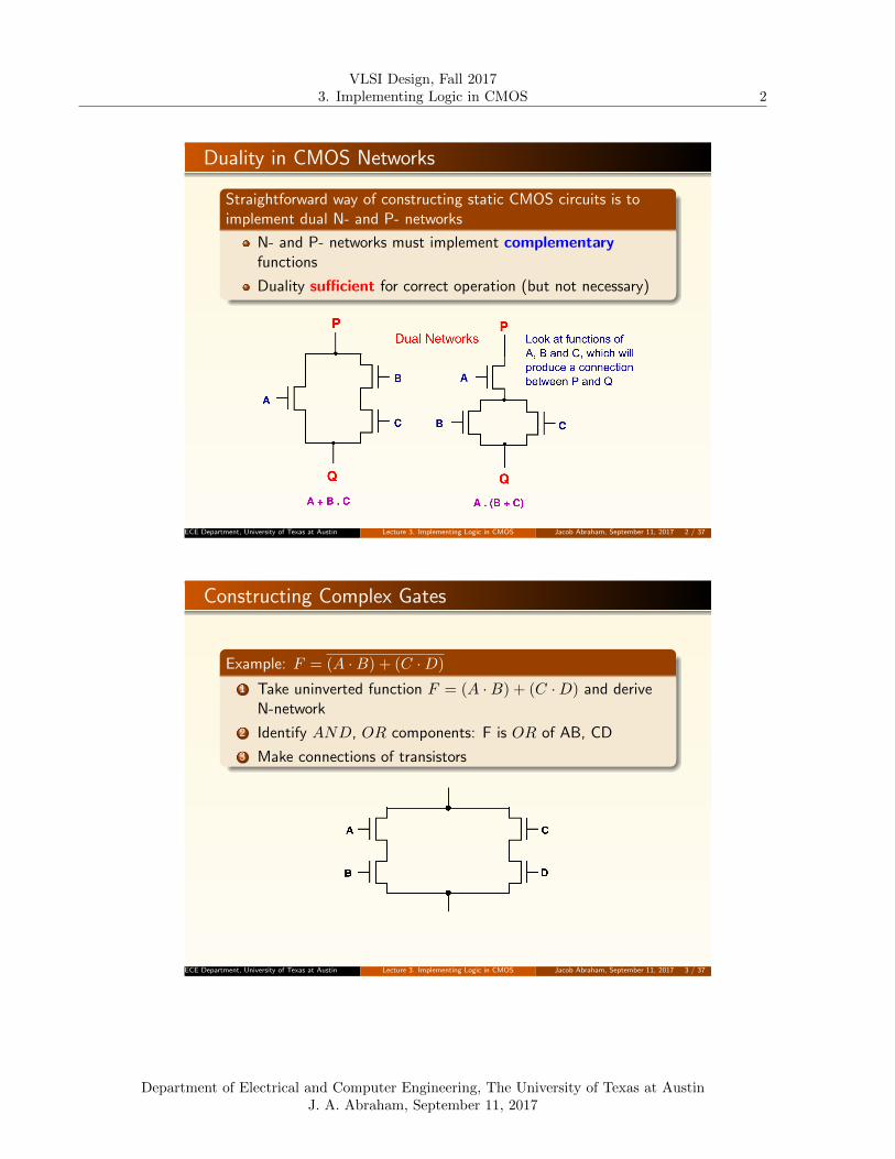
Duality in CMOS Networks
Straightforward way of constructing static CMOS circuits is toimplement dual N- and P- networks
N- and P- networks must implement complementaryfunctions
Duality sufficient for correct operation (but not necessary)
ECE Department, University of Texas at Austin Lecture 3. Implementing Logic in CMOS Jacob Abraham, September 11, 2017 2 / 37
Constructing Complex Gates
Example: F = (A ·B) + (C ·D)
1 Take uninverted function F = (A ·B) + (C ·D) and deriveN-network
2 Identify AND, OR components: F is OR of AB, CD
3 Make connections of transistors
ECE Department, University of Texas at Austin Lecture 3. Implementing Logic in CMOS Jacob Abraham, September 11, 2017 3 / 37
Department of Electrical and Computer Engineering, The University of Texas at AustinJ. A. Abraham, September 11, 2017
VLSI Design, Fall 20173. Implementing Logic in CMOS 3
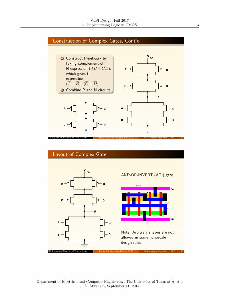
Construction of Complex Gates, Cont’d
4 Construct P-network bytaking complement ofN-expression (AB +CD),which gives theexpression,(A+B) · (C +D)
5 Combine P and N circuits
ECE Department, University of Texas at Austin Lecture 3. Implementing Logic in CMOS Jacob Abraham, September 11, 2017 4 / 37
Layout of Complex Gate
AND-OR-INVERT (AOI) gate
Note: Arbitrary shapes are notallowed in some nanoscaledesign rules
ECE Department, University of Texas at Austin Lecture 3. Implementing Logic in CMOS Jacob Abraham, September 11, 2017 5 / 37
Department of Electrical and Computer Engineering, The University of Texas at AustinJ. A. Abraham, September 11, 2017

VLSI Design, Fall 20173. Implementing Logic in CMOS 4
Example of Compound Gate
F = (A+B + C) ·D)
Note:
N- and P- graphs are duals of eachother
In this case, the function is thecomplement of the switchingfunction between F and GND
Question: Does it make anydifference to the function if thetransistor with input D is connectedbetween the parallel A, B, C,transistors and GND?
What about the electrical behavior?
ECE Department, University of Texas at Austin Lecture 3. Implementing Logic in CMOS Jacob Abraham, September 11, 2017 6 / 37
Example of More Complex Gate
OUT = (A+B) · (C +D) · (E + F + (G ·H))ECE Department, University of Texas at Austin Lecture 3. Implementing Logic in CMOS Jacob Abraham, September 11, 2017 7 / 37
Department of Electrical and Computer Engineering, The University of Texas at AustinJ. A. Abraham, September 11, 2017

VLSI Design, Fall 20173. Implementing Logic in CMOS 5
Example of More Complex Gate
OUT = (A+B) · (C +D) · (E + F + (G ·H))ECE Department, University of Texas at Austin Lecture 3. Implementing Logic in CMOS Jacob Abraham, September 11, 2017 7 / 37
Exclusive-NOR Gate in CMOS
Note: designs such as these should be checked very carefully forcorrect behavior using circuit simulation
ECE Department, University of Texas at Austin Lecture 3. Implementing Logic in CMOS Jacob Abraham, September 11, 2017 8 / 37
Department of Electrical and Computer Engineering, The University of Texas at AustinJ. A. Abraham, September 11, 2017

VLSI Design, Fall 20173. Implementing Logic in CMOS 6
Pseudo nMOS Logic
Based on the old NMOS technology where a “depletion” transistorwas used as a pullup resistor
What happens when there is no path from Z to ground (i.e., Z =1)?
What happens when there is a path from Z to ground (i.e., Z = 0)?
ECE Department, University of Texas at Austin Lecture 3. Implementing Logic in CMOS Jacob Abraham, September 11, 2017 9 / 37
Duality is Not Necessary for a CMOS Structure
Functions realized by N and P networks must be complementary,and one of them must conduct for every input combination
F = a ·b+a ·b+a ·c+c ·d+c ·dThe N and P networks areNOT duals, but the switchingfunctions they implementare complementary
ECE Department, University of Texas at Austin Lecture 3. Implementing Logic in CMOS Jacob Abraham, September 11, 2017 10 / 37
Department of Electrical and Computer Engineering, The University of Texas at AustinJ. A. Abraham, September 11, 2017
VLSI Design, Fall 20173. Implementing Logic in CMOS 7
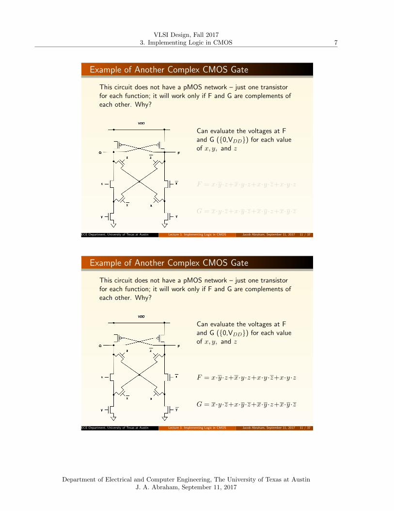
Example of Another Complex CMOS Gate
This circuit does not have a pMOS network – just one transistorfor each function; it will work only if F and G are complements ofeach other. Why?
Can evaluate the voltages at Fand G ({0,VDD}) for each valueof x, y, and z
F = x·y ·z+x·y ·z+x·y ·z+x·y ·z
G = x·y ·z+x·y ·z+x·y ·z+x·y ·z
ECE Department, University of Texas at Austin Lecture 3. Implementing Logic in CMOS Jacob Abraham, September 11, 2017 11 / 37
Department of Electrical and Computer Engineering, The University of Texas at AustinJ. A. Abraham, September 11, 2017
VLSI Design, Fall 20173. Implementing Logic in CMOS 8
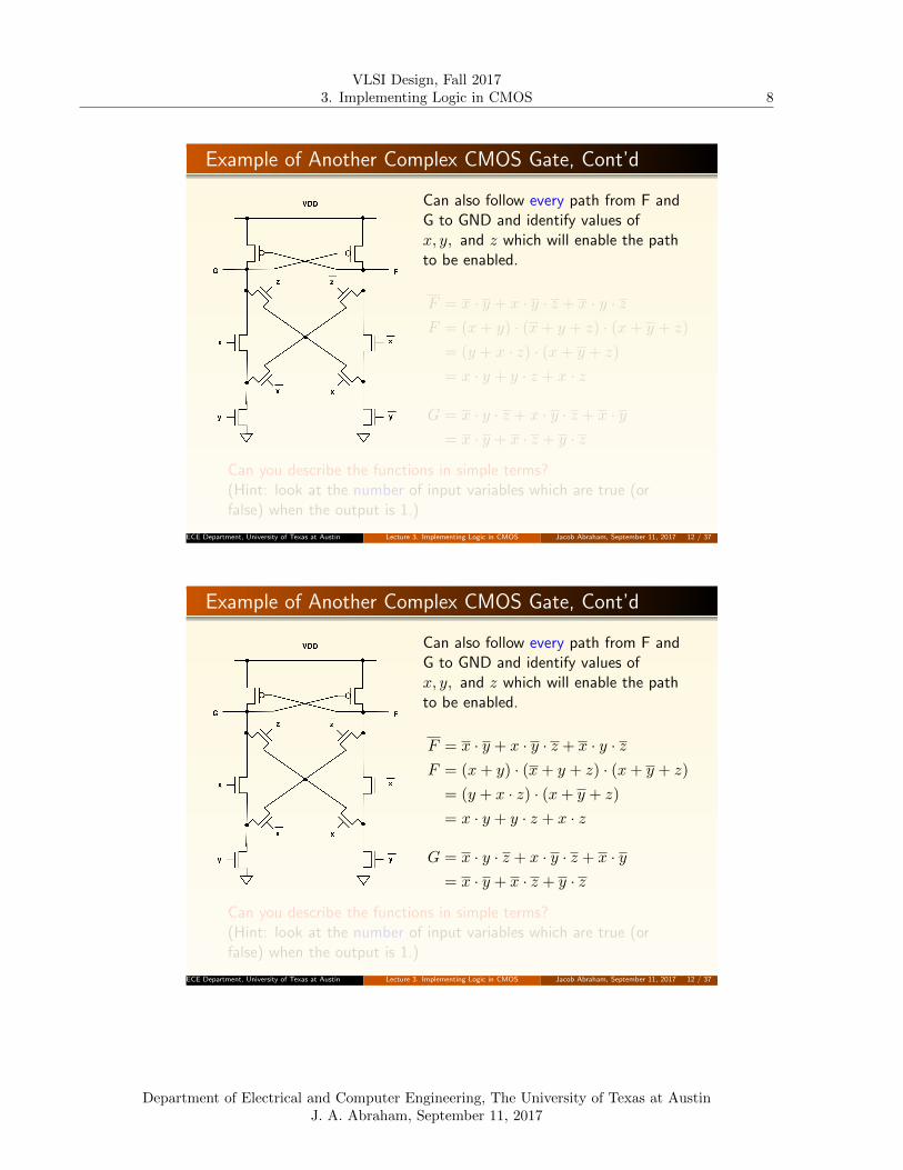
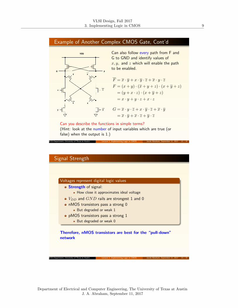
Example of Another Complex CMOS Gate, Cont’d
Can also follow every path from F andG to GND and identify values ofx, y, and z which will enable the pathto be enabled.
F = x · y + x · y · z + x · y · zF = (x+ y) · (x+ y + z) · (x+ y + z)
= (y + x · z) · (x+ y + z)
= x · y + y · z + x · z
G = x · y · z + x · y · z + x · y= x · y + x · z + y · z
Can you describe the functions in simple terms?(Hint: look at the number of input variables which are true (orfalse) when the output is 1.)
ECE Department, University of Texas at Austin Lecture 3. Implementing Logic in CMOS Jacob Abraham, September 11, 2017 12 / 37
Department of Electrical and Computer Engineering, The University of Texas at AustinJ. A. Abraham, September 11, 2017
VLSI Design, Fall 20173. Implementing Logic in CMOS 9
Example of Another Complex CMOS Gate, Cont’d
Can also follow every path from F andG to GND and identify values ofx, y, and z which will enable the pathto be enabled.
F = x · y + x · y · z + x · y · zF = (x+ y) · (x+ y + z) · (x+ y + z)
= (y + x · z) · (x+ y + z)
= x · y + y · z + x · z
G = x · y · z + x · y · z + x · y= x · y + x · z + y · z
Can you describe the functions in simple terms?(Hint: look at the number of input variables which are true (orfalse) when the output is 1.)
ECE Department, University of Texas at Austin Lecture 3. Implementing Logic in CMOS Jacob Abraham, September 11, 2017 12 / 37
Signal Strength
Voltages represent digital logic values
Strength of signal:
How close it approximates ideal voltage
VDD and GND rails are strongest 1 and 0
nMOS transistors pass a strong 0
But degraded or weak 1
pMOS transistors pass a strong 1
But degraded or weak 0
Therefore, nMOS transistors are best for the “pull-down”network
ECE Department, University of Texas at Austin Lecture 3. Implementing Logic in CMOS Jacob Abraham, September 11, 2017 13 / 37
Department of Electrical and Computer Engineering, The University of Texas at AustinJ. A. Abraham, September 11, 2017
VLSI Design, Fall 20173. Implementing Logic in CMOS 10
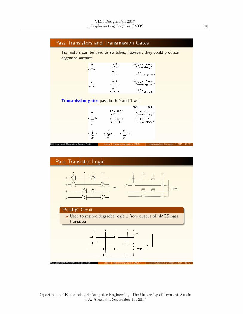
Pass Transistors and Transmission Gates
Transistors can be used as switches; however, they could producedegraded outputs
Transmission gates pass both 0 and 1 well
ECE Department, University of Texas at Austin Lecture 3. Implementing Logic in CMOS Jacob Abraham, September 11, 2017 14 / 37
Pass Transistor Logic
“Pull-Up” Circuit
Used to restore degraded logic 1 from output of nMOS passtransistor
ECE Department, University of Texas at Austin Lecture 3. Implementing Logic in CMOS Jacob Abraham, September 11, 2017 15 / 37
Department of Electrical and Computer Engineering, The University of Texas at AustinJ. A. Abraham, September 11, 2017
VLSI Design, Fall 20173. Implementing Logic in CMOS 11
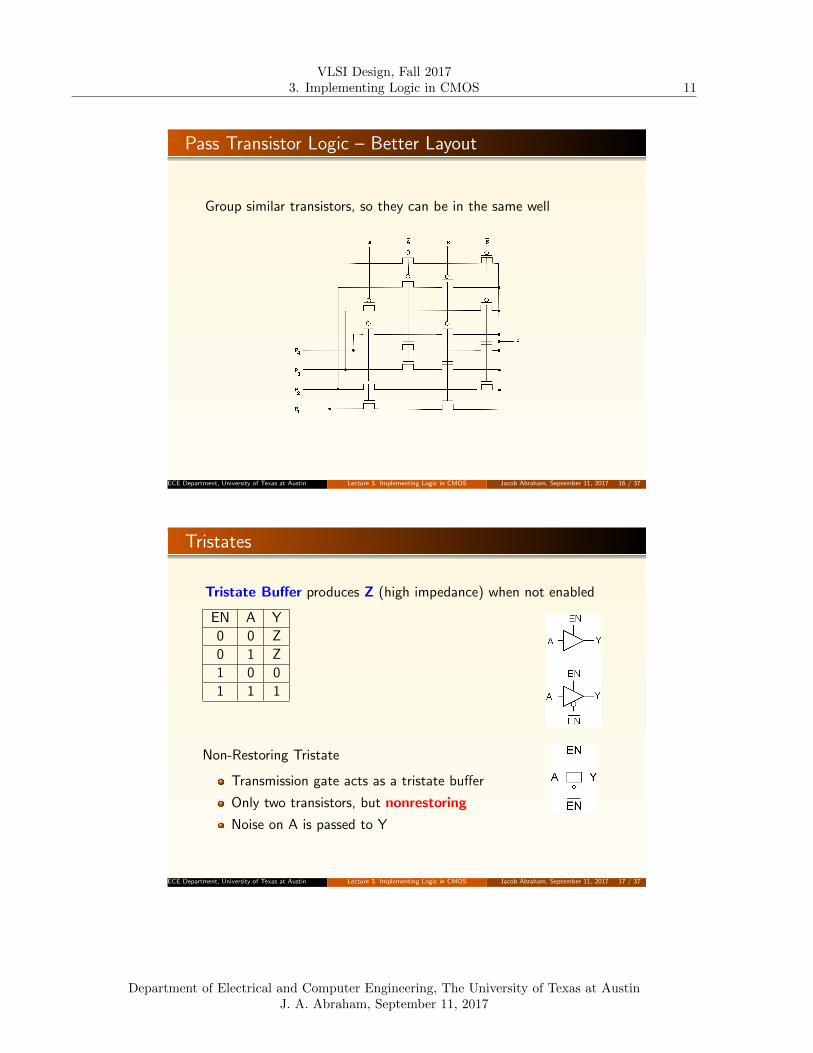
Pass Transistor Logic – Better Layout
Group similar transistors, so they can be in the same well
ECE Department, University of Texas at Austin Lecture 3. Implementing Logic in CMOS Jacob Abraham, September 11, 2017 16 / 37
Tristates
Tristate Buffer produces Z (high impedance) when not enabled
EN A Y
0 0 Z
0 1 Z
1 0 0
1 1 1
Non-Restoring Tristate
Transmission gate acts as a tristate buffer
Only two transistors, but nonrestoring
Noise on A is passed to Y
ECE Department, University of Texas at Austin Lecture 3. Implementing Logic in CMOS Jacob Abraham, September 11, 2017 17 / 37
Department of Electrical and Computer Engineering, The University of Texas at AustinJ. A. Abraham, September 11, 2017

VLSI Design, Fall 20173. Implementing Logic in CMOS 12
Tristate Inverter
Tristate inverter produces restored output, but complements signal
A
YEN
A
Y
EN = 0Y = 'Z'
Y
EN = 1Y = A
A
EN
ECE Department, University of Texas at Austin Lecture 3. Implementing Logic in CMOS Jacob Abraham, September 11, 2017 18 / 37
Multiplexers
S D1 D0 Y0 X 0 00 X 1 11 0 X 01 1 X 1
How many transistors are needed?(The better design uses 3 NANDgates and 1 inverter)
ECE Department, University of Texas at Austin Lecture 3. Implementing Logic in CMOS Jacob Abraham, September 11, 2017 19 / 37
Department of Electrical and Computer Engineering, The University of Texas at AustinJ. A. Abraham, September 11, 2017

VLSI Design, Fall 20173. Implementing Logic in CMOS 13
Transmission Gate MUX
Nonrestoring MUX
Uses two transmissiongates =⇒ only 4transistors
Inverting MUX – adds an inverter
Uses compound gate AOI22
Alternatively, a pair of tristate inverters (same thing)
ECE Department, University of Texas at Austin Lecture 3. Implementing Logic in CMOS Jacob Abraham, September 11, 2017 20 / 37
4:1 Multiplexer
A 4:1 MUX chooses one of 4 inputs using two selects
Two levels of 2:1 MUXes
Alternatively, four tristates
ECE Department, University of Texas at Austin Lecture 3. Implementing Logic in CMOS Jacob Abraham, September 11, 2017 21 / 37
Department of Electrical and Computer Engineering, The University of Texas at AustinJ. A. Abraham, September 11, 2017
VLSI Design, Fall 20173. Implementing Logic in CMOS 14
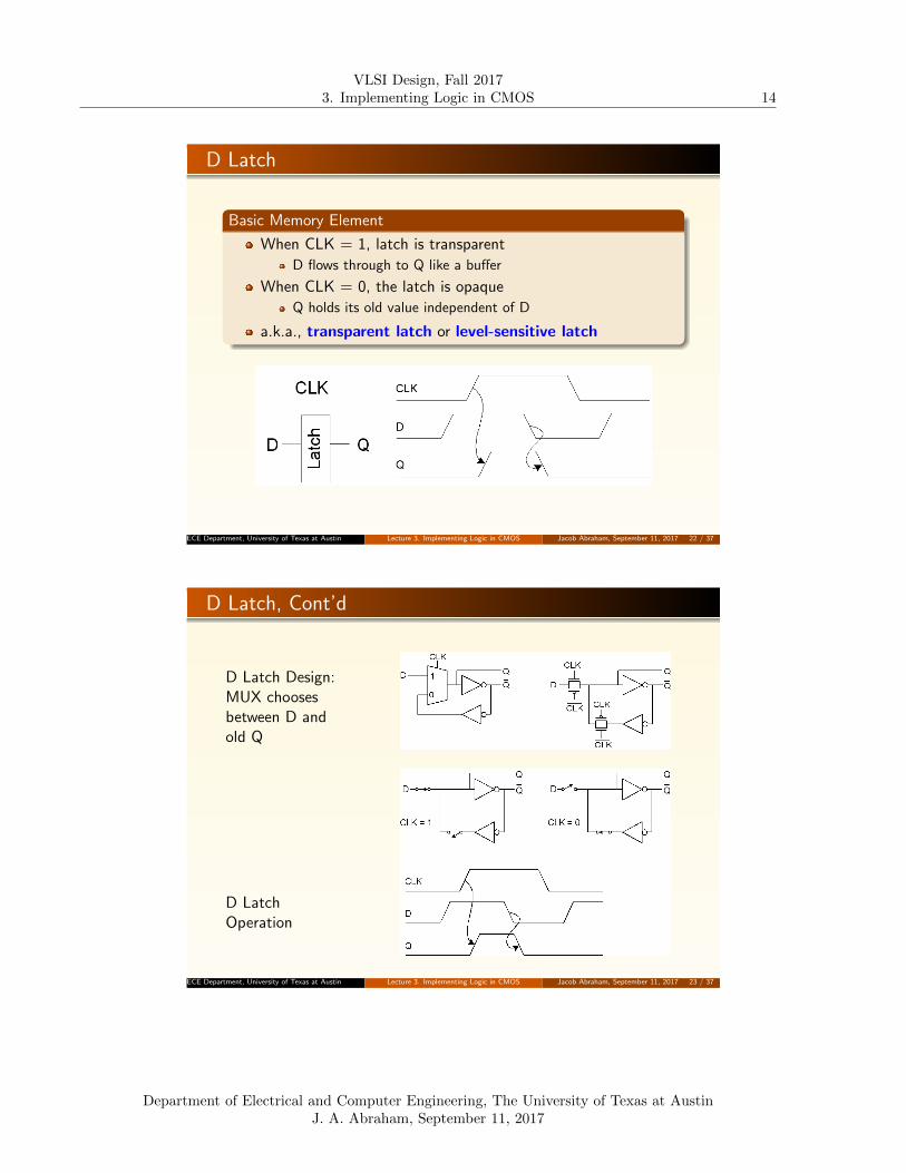
D Latch
Basic Memory Element
When CLK = 1, latch is transparent
D flows through to Q like a buffer
When CLK = 0, the latch is opaque
Q holds its old value independent of D
a.k.a., transparent latch or level-sensitive latch
ECE Department, University of Texas at Austin Lecture 3. Implementing Logic in CMOS Jacob Abraham, September 11, 2017 22 / 37
D Latch, Cont’d
D Latch Design:MUX choosesbetween D andold Q
D LatchOperation
ECE Department, University of Texas at Austin Lecture 3. Implementing Logic in CMOS Jacob Abraham, September 11, 2017 23 / 37
Department of Electrical and Computer Engineering, The University of Texas at AustinJ. A. Abraham, September 11, 2017
VLSI Design, Fall 20173. Implementing Logic in CMOS 15
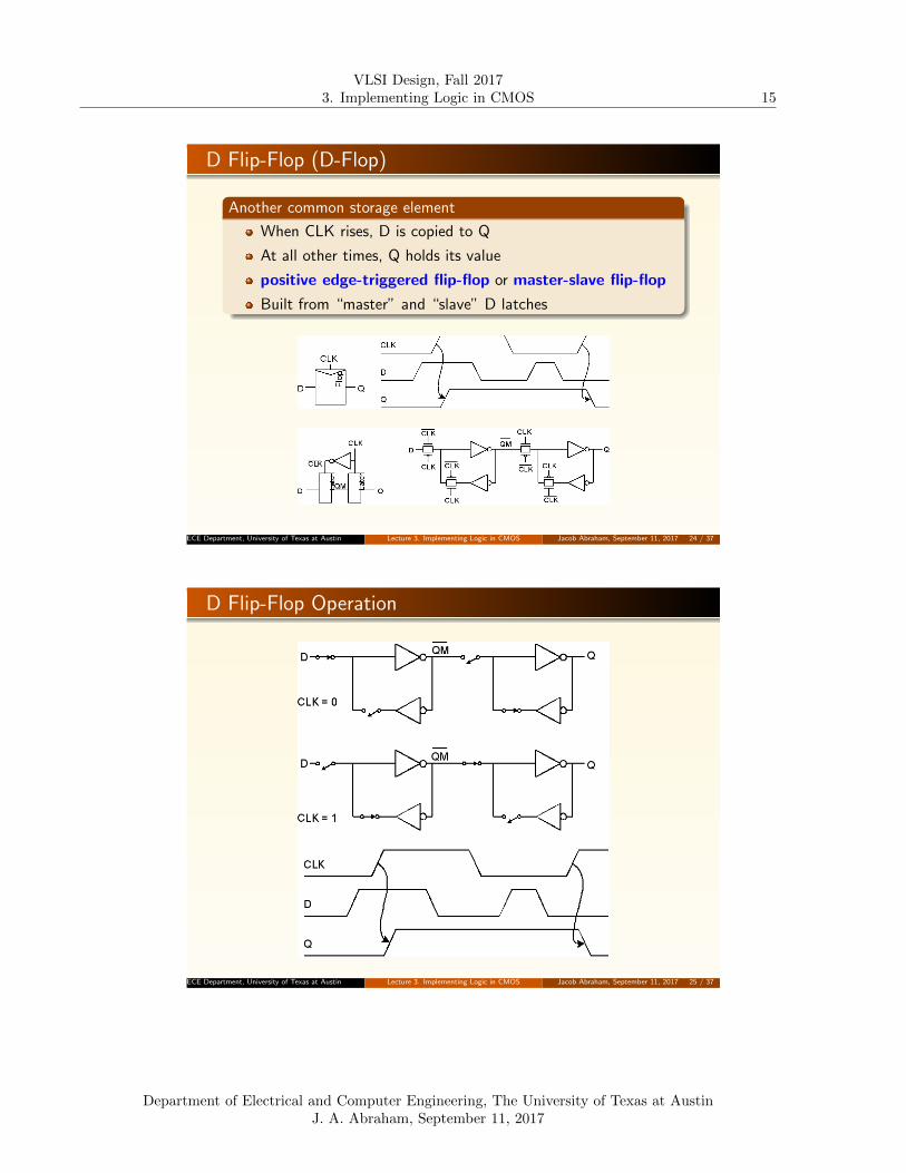
D Flip-Flop (D-Flop)
Another common storage element
When CLK rises, D is copied to Q
At all other times, Q holds its value
positive edge-triggered flip-flop or master-slave flip-flop
Built from “master” and “slave” D latches
ECE Department, University of Texas at Austin Lecture 3. Implementing Logic in CMOS Jacob Abraham, September 11, 2017 24 / 37
D Flip-Flop Operation
ECE Department, University of Texas at Austin Lecture 3. Implementing Logic in CMOS Jacob Abraham, September 11, 2017 25 / 37
Department of Electrical and Computer Engineering, The University of Texas at AustinJ. A. Abraham, September 11, 2017

VLSI Design, Fall 20173. Implementing Logic in CMOS 16
Race Condition – Hold Time Failure
Back-to-back flops can malfunction from clock skew
Second flip-flop fires late
Sees first flip-flop change and captures its result
Called hold-time failure or race condition
ECE Department, University of Texas at Austin Lecture 3. Implementing Logic in CMOS Jacob Abraham, September 11, 2017 26 / 37
Non-Overlapping Clocks
A simple way to prevent races
This works as long as non-overlap exceeds clock skew
Used in safe (conservative) designs
Industry does not generally use this approach – managingskew more carefully instead
ECE Department, University of Texas at Austin Lecture 3. Implementing Logic in CMOS Jacob Abraham, September 11, 2017 27 / 37
Department of Electrical and Computer Engineering, The University of Texas at AustinJ. A. Abraham, September 11, 2017
VLSI Design, Fall 20173. Implementing Logic in CMOS 17
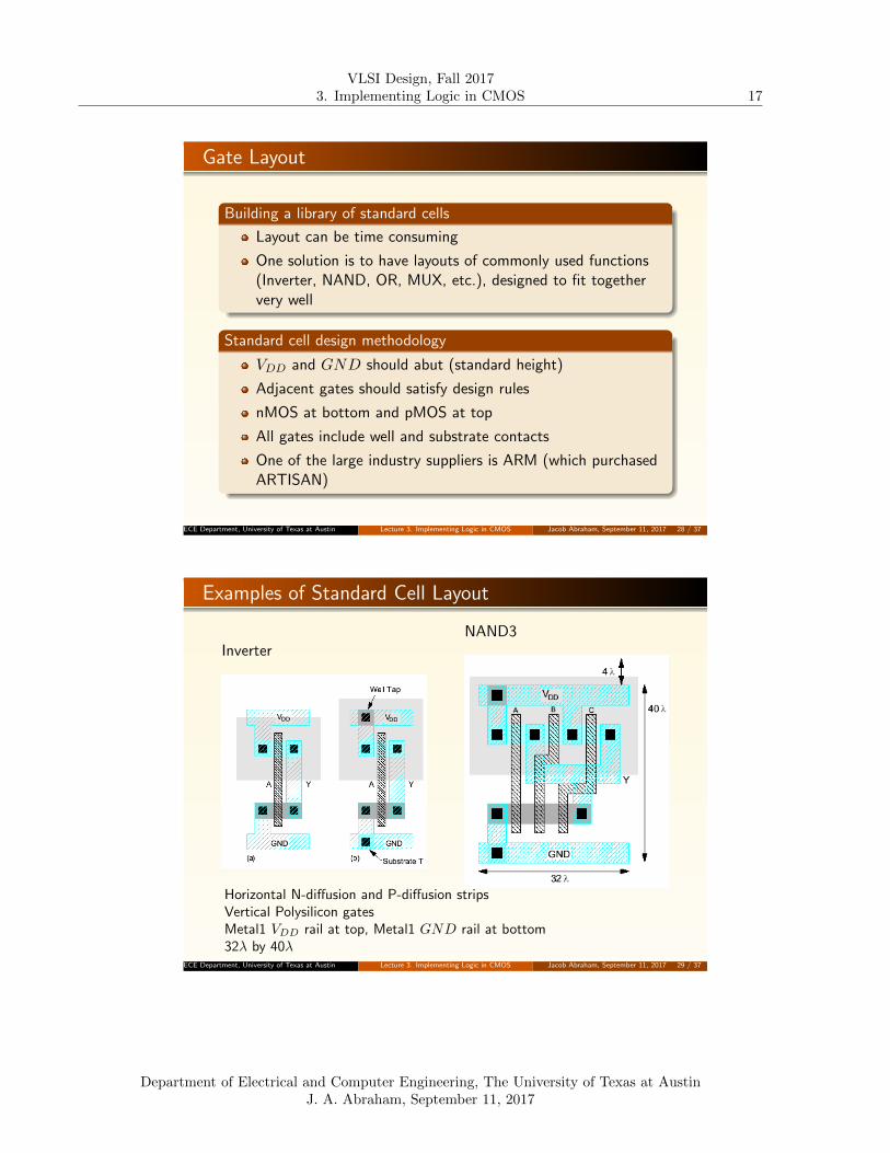
Gate Layout
Building a library of standard cells
Layout can be time consuming
One solution is to have layouts of commonly used functions(Inverter, NAND, OR, MUX, etc.), designed to fit togethervery well
Standard cell design methodology
VDD and GND should abut (standard height)
Adjacent gates should satisfy design rules
nMOS at bottom and pMOS at top
All gates include well and substrate contacts
One of the large industry suppliers is ARM (which purchasedARTISAN)
ECE Department, University of Texas at Austin Lecture 3. Implementing Logic in CMOS Jacob Abraham, September 11, 2017 28 / 37
Examples of Standard Cell Layout
InverterNAND3
Horizontal N-diffusion and P-diffusion stripsVertical Polysilicon gatesMetal1 VDD rail at top, Metal1 GND rail at bottom32λ by 40λ
ECE Department, University of Texas at Austin Lecture 3. Implementing Logic in CMOS Jacob Abraham, September 11, 2017 29 / 37
Department of Electrical and Computer Engineering, The University of Texas at AustinJ. A. Abraham, September 11, 2017
VLSI Design, Fall 20173. Implementing Logic in CMOS 18
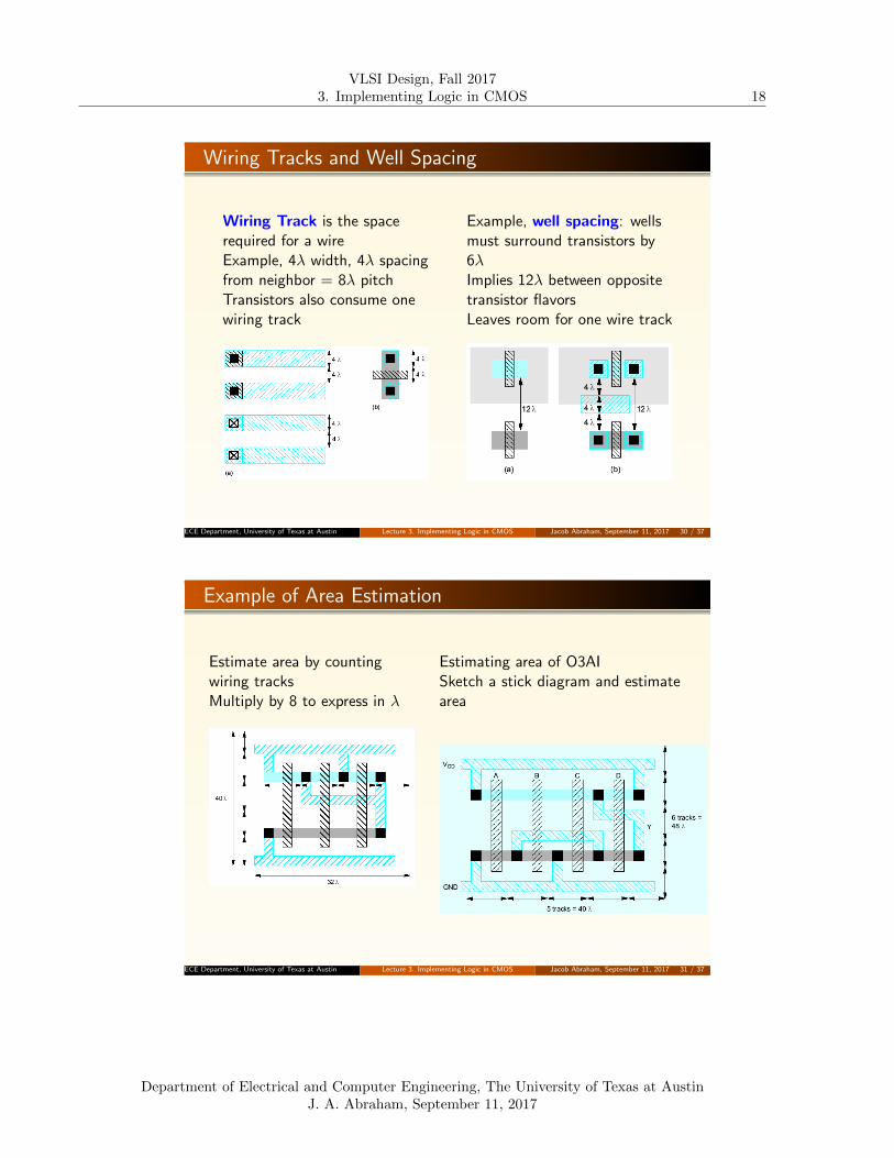
Wiring Tracks and Well Spacing
Wiring Track is the spacerequired for a wireExample, 4λ width, 4λ spacingfrom neighbor = 8λ pitchTransistors also consume onewiring track
Example, well spacing: wellsmust surround transistors by6λImplies 12λ between oppositetransistor flavorsLeaves room for one wire track
ECE Department, University of Texas at Austin Lecture 3. Implementing Logic in CMOS Jacob Abraham, September 11, 2017 30 / 37
Example of Area Estimation
Estimate area by countingwiring tracksMultiply by 8 to express in λ
Estimating area of O3AISketch a stick diagram and estimatearea
ECE Department, University of Texas at Austin Lecture 3. Implementing Logic in CMOS Jacob Abraham, September 11, 2017 31 / 37
Department of Electrical and Computer Engineering, The University of Texas at AustinJ. A. Abraham, September 11, 2017

VLSI Design, Fall 20173. Implementing Logic in CMOS 19
Example Circuit 1
Fill in the Karnaugh map to represent the Boolean functionimplemented by the pass-transistor circuit.
ECE Department, University of Texas at Austin Lecture 3. Implementing Logic in CMOS Jacob Abraham, September 11, 2017 32 / 37
Example Circuit 1
F(a,b,c,d,e):
00
01
12
13
14
15
06
07
18
19
010
011
012
013
114
115
016
017
118
119
120
121
022
023
124
025
026
127
028
129
130
031
a
b
c
d
e e
ECE Department, University of Texas at Austin Lecture 3. Implementing Logic in CMOS Jacob Abraham, September 11, 2017 33 / 37
Department of Electrical and Computer Engineering, The University of Texas at AustinJ. A. Abraham, September 11, 2017
VLSI Design, Fall 20173. Implementing Logic in CMOS 20
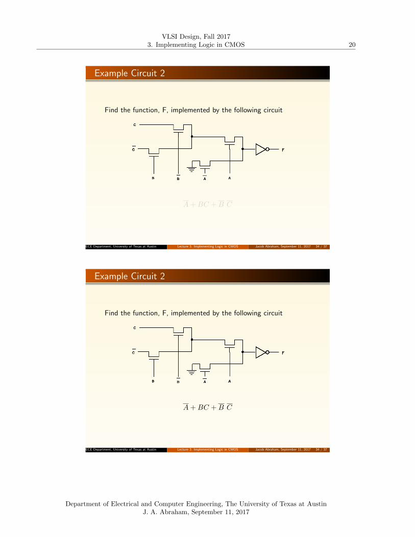
Example Circuit 2
Find the function, F, implemented by the following circuit
A+BC +B C
ECE Department, University of Texas at Austin Lecture 3. Implementing Logic in CMOS Jacob Abraham, September 11, 2017 34 / 37
Example Circuit 2
Find the function, F, implemented by the following circuit
A+BC +B C
ECE Department, University of Texas at Austin Lecture 3. Implementing Logic in CMOS Jacob Abraham, September 11, 2017 34 / 37
Department of Electrical and Computer Engineering, The University of Texas at AustinJ. A. Abraham, September 11, 2017

VLSI Design, Fall 20173. Implementing Logic in CMOS 21
Example Circuit 3
Find the functions X and Y implemented by the following circuit
ECE Department, University of Texas at Austin Lecture 3. Implementing Logic in CMOS Jacob Abraham, September 11, 2017 35 / 37
Example Circuit 3
Find the functions X and Y implemented by the following circuit
ECE Department, University of Texas at Austin Lecture 3. Implementing Logic in CMOS Jacob Abraham, September 11, 2017 36 / 37
Department of Electrical and Computer Engineering, The University of Texas at AustinJ. A. Abraham, September 11, 2017

VLSI Design, Fall 20173. Implementing Logic in CMOS 22
Functions to Circuits
Label the circuit so that it implements the function:F = a · (b · c+ b · c)
ECE Department, University of Texas at Austin Lecture 3. Implementing Logic in CMOS Jacob Abraham, September 11, 2017 37 / 37
Department of Electrical and Computer Engineering, The University of Texas at AustinJ. A. Abraham, September 11, 2017