3 experimental and characterization methods · 2003-03-11 · 3 experimental and characterization...
TRANSCRIPT

3 Experimental and characterization
methods
3.1 Pulsed laser deposition
3.1.1 Introduction and principle
A number of techniques are now available to produce high quality thin films of ferroelectrics (see
Table 3.1). Thermal evaporation (TE) represents a physical vapor deposition process using a heated
crucible or an electron beam evaporator as the vapor source[62]. Sputter deposition (S) is performed
by extracting ions from a plasma at keV energies that strike a target consisting of the material to
be deposited[63]. Molecular beam epitaxy (MBE) uses continuous molecular beams generated by
Knudsen sources[64; 65]. The deposition flux in chemical vapor deposition (CVD) is derived from
the reaction of two or more gaseous chemicals on or above a heated substrate[66]. Heaters above
the substrate provide the energy necessary to sustain the reaction. Metal organic chemical vapor
deposition (MOCVD) is similar to CVD, except that the reacting gases are metal-organic compounds
that widen the range of materials that can be deposited by normal CVD.
Table 3.1: Most known deposition processes.
Technique Acronym Experimental purpose Reference
Thermal evaporation TE optics, protective coatings, [67]
electronic materials
Sputtering S electronic materials, optics, [68; 69; 70]
(RF, magnetron, ion beam) protective coatings
Molecular beam epitaxy MBE electronic materials [71; 72; 7]
[73; 74; 75]
Chemical vapor deposition CVD protective coatings, structural [76]
and electronic materials
Metal-organic MOCVD electronic materials [77; 78; 79; 80]
chemical vapor deposition [81; 82; 83; 84]
Pulsed Laser Deposition PLD electronic materials [85; 86; 87]

3.1 Pulsed laser deposition 20
Physical vapor deposition techniques such as plasma and ion beam sputter deposition and pulsed laser
ablated deposition are extensively used for synthesizing single and multicomponent and multilayered
thin films[88]. The development of PLD has moved rapidly since the discovery of high-temperature
superconductor oxides in 1986[89]. These oxides have a perovskite-based crystal structure similar
to many ferroelectric materials and have been deposited as epitaxial films by, e.g., PLD[90]. This
deposition technique offers a number of advantages over the other techniques used for the preparation
of thin films of ferroelectrics; in particular, epitaxial films can be deposited at rather low substrate
temperatures and high deposition rates, over a large range of target phases and compositions, and
with few experimental parameters to optimize. An automated PLD technique involves ablation of
elemental targets (metals or their oxides) sequentially exposed to an excimer laser beam using a
computer-controlled system.
The physical phenomena involved in the interaction of high-power nanosecond excimer-laser
pulses with bulk targets resulting in evaporation, plasma formation, and subsequent deposition of
thin films were studied by Singh and Narayan[91; 92]. They developed a theoretical model for simu-
lating the laser-plasma-solid interaction. Based on the nature of interaction of the laser beam with the
target and the evaporated material, the pulsed laser evaporation process has been divided into three
separate regimes: (i) interaction of the laser beam with the bulk target, (ii) plasma formation, heating,
and initial three-dimensional isothermal expansion, and (iii) adiabatic expansion of the plasma and
deposition of thin films (Fig. 3.1). The first two processes occur during the time interval of the laser
pulse, while the last process begins after the laser pulse has terminated.
Fig. 3.1: Schematic diagram ofthe laser interaction with theplasma target showing differentphases[91]: (I) unaffected bulktarget, (II) evaporated target sur-face, (III) dense plasma absorp-tion of the laser radiation, and(IV) expanding plasma.
Thus the impact of the laser beam on the target surface results in a complex process including ab-
lation, melting, and evaporation of material, and producing a plasma due to excitation and ionization
of the species ejected from the target by the laser photons. All these processes are triggered by the
transformation of electromagnetic energy into electronic excitation, followed by a transformation into
thermal, chemical, and mechanical energy. The materials ejected from the target are finally deposited
onto a substrate.
Device structures which have been fabricated using PLD-grown ferroelectric thin films include
non-volatile random access memory (NVRAM) test structures with oxide electrodes[93], surface
acoustic wave (SAW) devices[94], tunable radio frequency (RF) phase shifters[95], acoustic wave

3.1 Pulsed laser deposition 21
transducers[96], electro-optic switches[97], and pyroelectric sensors[98]. A recently renewed interest
in ferroelectric thin films can be observed due to their potential with respect to smart materials and
active sensors in smart devices[99]. In fact, new applications for ferroelectrics will likely be conceived
as the ability to prepare high quality films with specific properties is realized[100]. PLD is already
making impact in this developing field by combining several materials in view of discovering new
materials with improved properties. The versatility of the PLD technique is demonstrated by the fact
that close to 128 different materials have been deposited as thin films[101]. For example, PLD can
be used advantageously to synthesize high-quality multicomponent oxide thin films including ferro-
electrics, high-temperature superconductors, electro-optic and optical materials[102; 93]. A balanced
description of advantages and disadvantages of the PLD technique to synthesize high temperature
superconductors and ferroelectric films has been presented in several reviews[103; 104; 105; 87]. Key
advantageous features of the PLD technique include: (1) the possibility of a straightforward trans-
fer, under certain conditions, of a target stoichiometry to the film; (2) the ability to deposit in high
background pressures, which in this case minimizes vaporization of volatile species from the film; (3)
the ease of deposition at elevated substrate temperature which enables epitaxial film growth and can
minimize the thermal budget during processing, and (4) the demonstrated high deposition rate (about
10 Å/s).
Preparation of (Ba,Sr)TiO3 thin films has been carried out by reactive evaporation[106], rf-sput-
tering[107], metal organic chemical vapor deposition[8], sol-gel[3], and laser ablation methods[4]. The
main problem of MOCVD for BaO, SrO, or rare earth-based oxides is the poor volatility and thermal
stability of the precursors. Different approaches, mainly using a liquid source, have been proposed to
solve this problem. Pulsed liquid-injection MOCVD deposition permits the generation of a stable gas
phase from unstable precursors. By adjusting the injection parameters and the molar concentration
of the solutions, a “layer-by-layer”growth mode can be approached. This technique is based on the
computer-controlled injection of micro-droplets of precursor solution into the evaporator system. In
recent years, PLD was developed as a significant method to study the growth processes of oxide thin
films.
3.1.2 PLD system
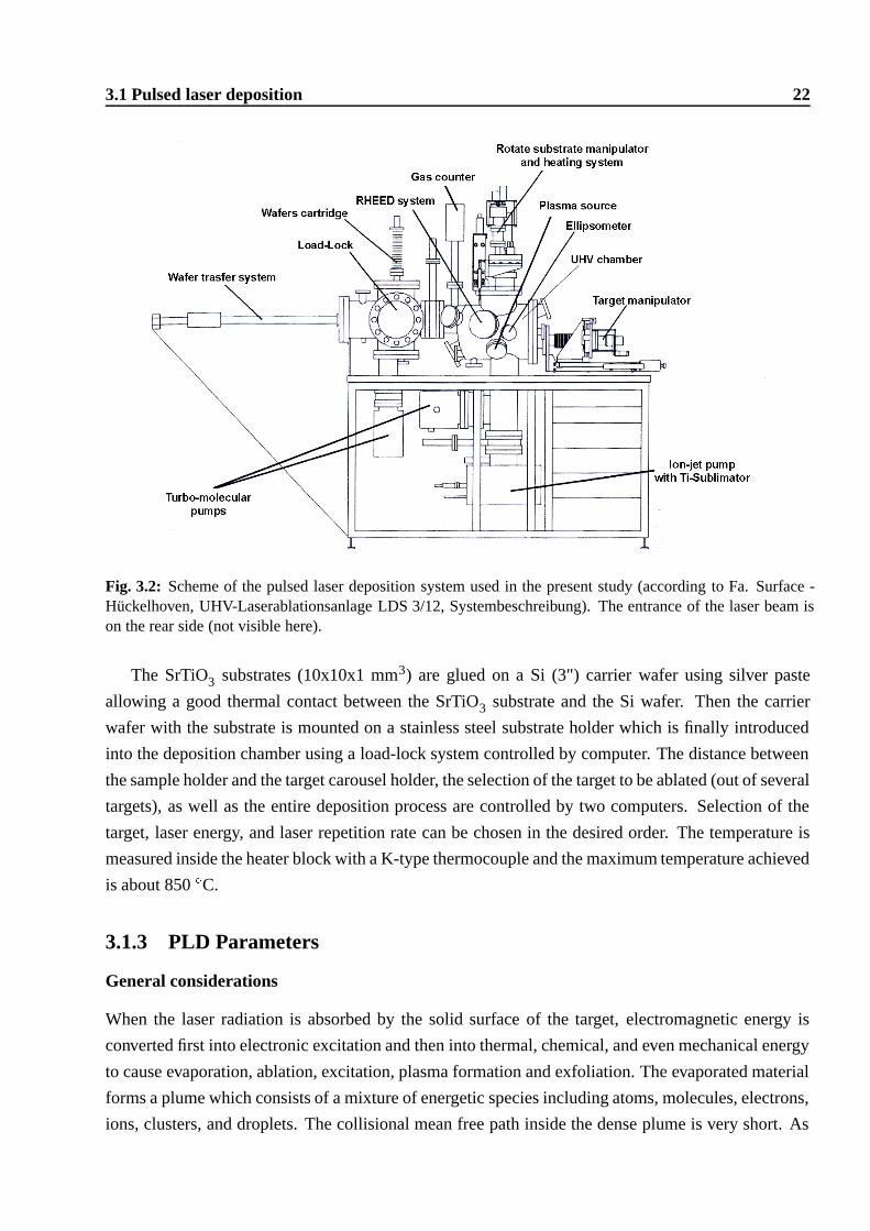
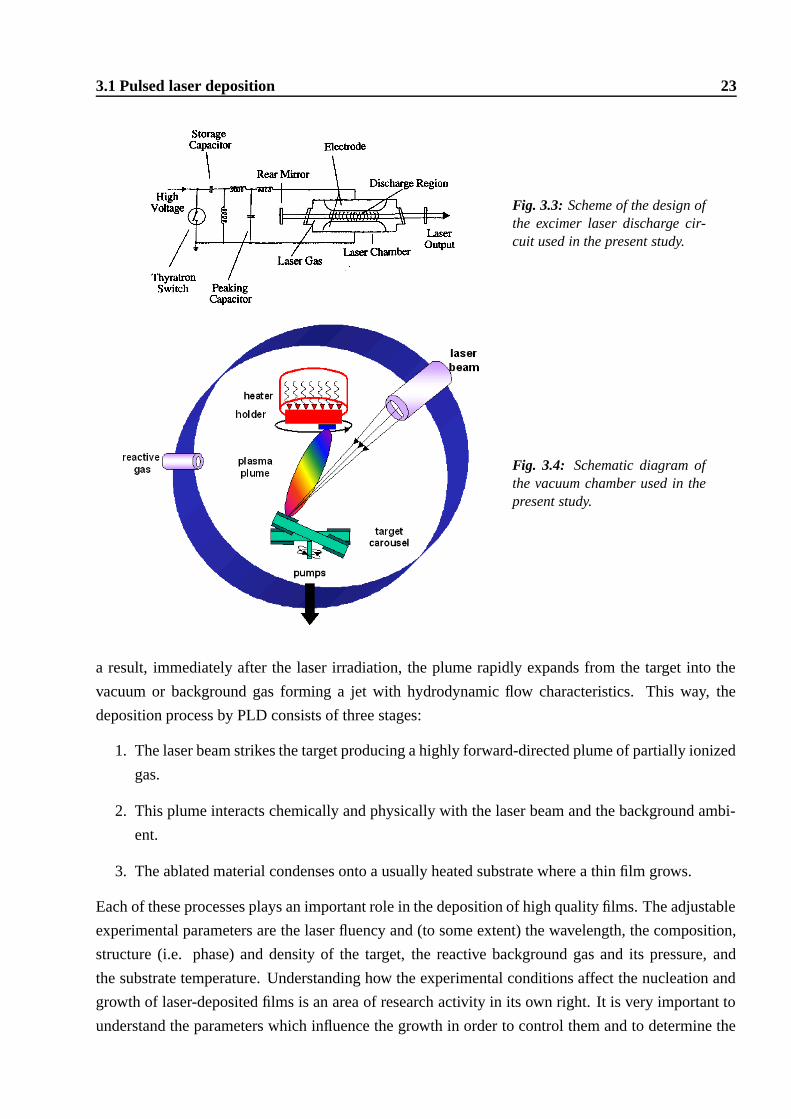
The PLD system used in the present study is schematically shown in Fig. 3.2. This PLD system
consists of a KrF excimer laser (λ = 248 nm, λ - wavelength of the emitted radiation) (Fig. 3.3) and
a UHV system in turn consisting of a load lock and a deposition chamber.
The laser beam is directed onto the target by an optical system of lenses. The lens and window
materials are chosen to minimize any absorbtion of laser light and thus to ensure a maximum attain-
able laser energy on the target. The laser beam is focused at an angle of 45Æ onto one out of four
pressed ceramic powder targets (e.g., BaTiO3 or SrTiO3 targets) located in the vacuum chamber (Fig.
3.4).
3.1 Pulsed laser deposition 22
Fig. 3.2: Scheme of the pulsed laser deposition system used in the present study (according to Fa. Surface -Hückelhoven, UHV-Laserablationsanlage LDS 3/12, Systembeschreibung). The entrance of the laser beam ison the rear side (not visible here).
The SrTiO3 substrates (10x10x1 mm3) are glued on a Si (3") carrier wafer using silver paste
allowing a good thermal contact between the SrTiO3 substrate and the Si wafer. Then the carrier
wafer with the substrate is mounted on a stainless steel substrate holder which is finally introduced
into the deposition chamber using a load-lock system controlled by computer. The distance between
the sample holder and the target carousel holder, the selection of the target to be ablated (out of several
targets), as well as the entire deposition process are controlled by two computers. Selection of the
target, laser energy, and laser repetition rate can be chosen in the desired order. The temperature is
measured inside the heater block with a K-type thermocouple and the maximum temperature achieved
is about 850 ÆC.
3.1.3 PLD Parameters
General considerations
When the laser radiation is absorbed by the solid surface of the target, electromagnetic energy is
converted first into electronic excitation and then into thermal, chemical, and even mechanical energy
to cause evaporation, ablation, excitation, plasma formation and exfoliation. The evaporated material
forms a plume which consists of a mixture of energetic species including atoms, molecules, electrons,
ions, clusters, and droplets. The collisional mean free path inside the dense plume is very short. As
3.1 Pulsed laser deposition 23
Fig. 3.3: Scheme of the design ofthe excimer laser discharge cir-cuit used in the present study.
Fig. 3.4: Schematic diagram ofthe vacuum chamber used in thepresent study.
a result, immediately after the laser irradiation, the plume rapidly expands from the target into the
vacuum or background gas forming a jet with hydrodynamic flow characteristics. This way, the
deposition process by PLD consists of three stages:
1. The laser beam strikes the target producing a highly forward-directed plume of partially ionized
gas.
2. This plume interacts chemically and physically with the laser beam and the background ambi-
ent.
3. The ablated material condenses onto a usually heated substrate where a thin film grows.
Each of these processes plays an important role in the deposition of high quality films. The adjustable
experimental parameters are the laser fluency and (to some extent) the wavelength, the composition,
structure (i.e. phase) and density of the target, the reactive background gas and its pressure, and
the substrate temperature. Understanding how the experimental conditions affect the nucleation and
growth of laser-deposited films is an area of research activity in its own right. It is very important to
understand the parameters which influence the growth in order to control them and to determine the

3.1 Pulsed laser deposition 24
film properties, such as orientation, microstructure, and dielectric properties. A discussion of these
parameters is the subject of this section.
Target material
Ideally, when ablating the target, the laser should cause a stoichiometric transfer of the compo-
sition of the target to the growing film. Complex-oxide targets are usually obtained from sintering
mixtures of the component metal oxides or from calcination of oxide powders. “Fully reacted” tar-
gets result from a complete solid-state reaction during the sintering process, whereas “pressed-oxide”
targets result only from a mechanical process. Since sintering takes place at high temperatures, it
is possible that volatile components of the target may be lost during this process, especially at the
surface. Usually the pressed-oxide targets are processed at much lower temperatures (below 600 ÆC)
than the fully reacted targets, and therefore are less affected by losses of volatile components[108].
In order to stabilize the target, the deposition process is typically preceded by a target “burn-
in”, during which the target is irradiated by several laser shots prior to using it for the film growth.
The purpose of this process is to expose fresh material, and maintain a steady-state composition at
the target surface. The surface composition may differ from that in the interior of the target due to
segregation phenomena that may occur during target ablation. This burn-in process should be repeated
whenever the ambient gas conditions are changed because the segregation process is sensitive to the
ambient.
A disadvantage of PLD, in general, is the presence of droplets on the substrate surface. The
droplets generated by laser ablation can be due to: (i) protrusions, pits, craters or microcracks that
exist in a fresh target or are progressively formed after substantial laser irradiation, being removed
from the target due to the thermal and mechanical shock induced by the laser; (ii) rapid expansion of
trapped vapor bubbles beneath the surface during laser irradiation, causing forced ejection of surface
material; (iii) splashing of the molten layer near the upper surface of the target due to rapid surface
evaporation (most commonly observed in case of use of high-power lasers); (iv) condensation of va-
por material due to supersaturation (most likely observed in case of use of high gas pressure). Many
attempts have been made to avoid the presence of droplets. In case of metals two kinds of droplets
(depending on the expelling place, that is from the cones growing out of the target or from the molten
surface) have been observed, which have different sizes, angular distributions, velocities, and depen-
dencies on the number of pulses, the roughness of the target and the density of the laser energy[109].
The stoichiometry of the oxide targets plays an important role in the density of droplets [110].
Substrate temperature
The role of the substrate temperature in controlling structure and composition of the film is a pri-
mary one. Effects of the substrate temperature appear to be most important in obtaining a particular
crystal structure and orientation. E.g., a minimum temperature is usually required to grow crystalline
3.1 Pulsed laser deposition 25
films rather than amorphous, or epitaxial films rather than polycrystalline. This temperature should be
below the temperature at which extensive vaporization of volatile film components occurs. The ther-
mal energy that the condensing species attain on the substrate surface allows to increase the surface
mobility and the energy for nucleation and growth of the film. At a particular temperature necessary
for these processes to successfully occur, however, some volatile components may not stick to the
substrate and/or some may evaporate after incorporation into the film.
Several research groups prepared thin films at near room temperature (conditions typically re-
quired for stoichiometric, but amorphous materials) followed by post-deposition annealing at high
temperature to recrystallize the material and to induce ferroelectricity. The polycrystalline films that
result from post-deposition treatments may not be fully crystallized and are typically neither oriented
nor dense. In-situ deposition, positioning the substrate onto a heated stage, is the preferable approach
to achieve high quality film growth and can yield dense and epitaxial films.
However, measurement of the true substrate temperature is difficult. Therefore, a temperature
window for optimum film growth is frequently given in terms of the temperature of the heater.
Each ferroelectric material appears to have a distinct substrate temperature range that is optimum
for epitaxial film growth, falling roughly within a 550 ÆC to 800 ÆC window or even higher. BaTiO3
was reported to grow epitaxially at temperatures ranging from 670 ÆC to 750 ÆC on MgO by Norton et
al.[111]. Davis and Gower[112] found that BaTiO3 will not grow epitaxially at temperatures below 600ÆC. c-axis textured BaTiO3 films were deposited at a substrate temperature as low as 600 ÆC by Lin et
al.[113]. Although depositions performed at 750 ÆC on MgO and SrTiO3 substrates yielded the (001)
orientation of the BaTiO3 films, detailed analysis revealed that the crystallinity of films deposited
on SrTiO3 substrates is clearly superior to that of films deposited on MgO substrates. Low substrate
temperatures (550� 650 ÆC) tend to induce the growth of (110) grains. Non-(001) orientations appear
when the oxygen pressure is either too low or too high.
Oxygen partial pressure
At a given substrate temperature, the incorporation of a volatile atom into the film is greatly
dependent upon the pressure of the oxidizing atmosphere. This can be understood from the decrease
in vapor pressure observed for metals when they become oxidized. The ambient gas, however, must
not only help to keep the atoms on the surface once they arrive, but must also contribute to avoid
oxygen losses. In-situ fabrication of oxide thin films is generally carried out in an oxygen ambient.
Oxygen atoms, ions or molecules in the deposition chamber react with the plume and thus contribute
to an optimal oxygen content in the thin film during growth.
At low gas pressure, the scattering of the ejected species by the gas atoms or molecules is the
dominant process that determines the relative Ba/Ti content of the deposited films, while at high oxy-
gen pressure, the combination of the initial scattering and the further diffusion that takes place once
the injected species have been thermalized is the process that determines the film composition [114].

3.1 Pulsed laser deposition 26
Norton and Carter deposited BaTiO3 films on (100) MgO substrates using different oxygen partial
pressure and they studied the nucleation and growth of BaTiO3 by transmission electron microscopy
observing two different microstructures as a function of pressure[111]: Higher oxygen pressure (�
0.40 torr) yielded epitaxial film growth, while lower pressures gave rise to polycrystalline films.
The preferred orientation of thick BaTiO3 films was found to depend on the deposition pressure[115].
A (100)-orientation was developed below 1 mTorr deposition pressure, while the (110)-orientation
was found above 200 mTorr deposition pressure. During the deposition between 50 and 100 mTorr,
the preferred orientation varied between (111), (110), and (100). It has been observed that the growth
of a c-axis-oriented BaTiO3 film is favoured by a lower oxygen pressure, while the growth of an a-
axis-oriented BaTiO3 film is favoured by a higher oxygen pressure[116]. The lattice constant normal
to the substrate decreases with increasing oxygen pressure, probably due to a particle bombardment
mechanism and=or thermal vibrations. Moreover, a higher deposition temperature results in an in-
creased mobility of the adsorbed BaTiO3 clusters and in a better film recrystallization.
Different temperature and oxygen pressure conditions which have been used by different groups
are summarized in Table 3.2.
Table 3.2: Different deposition conditions for BaTiO3 films used in PLD.
author[reference] substrate temperature (ÆC) oxygen pressure (mbar)
Davis[112] MgO (100) 575 -SrTiO3 (110) 850 -
LiF (100) 600 -
Ito[117] MgO (100) 650 � 700 0.05
Kim[115] Pt=SiO2=Si 700 0.0013 � 0.26
Gonzalo[114] MgO (100) 700 1Si (100) RT 10�7
Hwang[118] Pt/Ti/SiO2/Si (100) 750 0.13
Srikant[119] MgO (001) 700 � 750 0.13 � 0.26
Kim[120] MgO, LaAlO3, Pt/Ti/SiO2/Si 500 � 800 0.4
Khan[121] SrTiO3 (100) 650 0.26sapphire (0001) 700 0.26
Suzuki[122] SrTiO3 700 0.01
Beckers[123] MgO (001) 1000 0.004
Lin[113] MgO (001) 750 0.1SrTiO3 (001) 750 0.1
YBCO/CeO2/SrTiO3 (001) 730 0.1
Liu[124] MgO (100) 750 0.1YBCO/SrTiO3 (001) 750 0.15
Boikov[125] MgO, LaAlO3, SrRuO3 (100) 740 � 785 0.4

3.1 Pulsed laser deposition 27
Film-substrate lattice mismatch
While the substrate temperature is an important parameter for deposition to obtain epitaxial films,
the mismatch between the lattice constants of film and substrate is equally critical. The lattice mis-
match is defined as shown in eq. 2.6. Epitaxial film growth occurs most readily when the lattice
spacing and symmetry of the substrate closely match those of the desired film.
In fact, the requirements to the substrate are even more complicated. Thus, substrates should have
thermal expansion coefficients close to that of the oxide film material, otherwise due to shock during
thermal cycling, the grown films are known to develop microcracks leading to discontinuities in the
films. Another requirement for the substrate material is to be chemically compatible in terms of the
nature of the chemical bonds.
Several usual substrates and their mismatch with respect to the BaTiO3 lattice constants have been
summarized in Table 3.3.
Table 3.3: Lattice mismatch between BaTiO3 film and several substrates.
Substrate Structure Lattice constant Mismatch with BaTiO3BaTiO3 tetragonal a = b = 3.994 Å
(perovskite structure) c = 4.038 ÅSrTiO3 cubic ac = 3.905 Å 2.28 % along a-direction
(perovskite structure) 3.4 % along c-directionMgO cubic ac = 4.212 Å -5.17 % along a-direction
(NaCl structure) -4.13 % along c-directionAl2O3 trigonal a = 5.14 Å -22.29 % along a-direction
(sapphire structure) -21.44 % along c-directionYSZ cubic ac = 5.16 Å -22.59 % along a-direction
(fluorite structure) -21.74 % along c-directionSi cubic ac = 5.43 Å -26.44 % along a-direction
(diamond structure) -25.63 % along c-directionYBa2Cu3O7 perovskite- a = 3.83 Å 4.28 % along a-direction
-derived b = 3.89 Å 2.67 % along b-directionstructure c = 11.68 Å -65.42 % along c-direction
LaAlO3 rhombohedral a = 5.364 Å -25.54 % along a-direction(perovskite structure) c = 13.11 Å -69.19 % along c-direction
It was observed that epitaxial BaTiO3 deposited by PLD shows different growth mechanisms on
different substrates because of different lattice mismatch. For example, BaTiO3 was reported to grow
on MgO (cubic, ac = 0.4231 nm) following an island growth mode[111], whereas BaTiO3 thin films
grown on SrTiO3 substrates seems to follow the layer-by-layer mode[6].
A dependence of the lattice parameter on film thickness was reported for an epitaxial system with
a small lattice mismatch such as BaTiO3 on SrTiO3[107; 126; 127; 73; 74]. In this case, if the thickness

3.1 Pulsed laser deposition 28
of the BaTiO3 film is under a certain critical value, the epitaxial film can grow two-dimensionally,
whereas when the thickness exceeds a critical value misfit dislocations are introduced, lattice relax-
ation occurs, and the lattice parameter of the film becomes (almost) equal to that of the bulk.
Target-substrate distance
Thickness and composition of the thin films grown by PLD are functions of the distance between
the target and the substrate. The laser-evaporated neutral and ionized particles travel at a speed of
about 106 cm/s in vacuum[128]. As the oxygen partial pressure increases, the velocity of these parti-
cles decreases due to collisions. If the substrate-to-target distance is small, the grown films are known
to contain large number of particulates (droplets).
An optimal distance of 4 - 7 cm was used by various groups.
Laser energy and repetition rate
When a target is bombarded with ions, electrons, single photons, or pulsed photons (called laser
pulses), a mechanism of particle emission is generated. This mechanism is called ablation or de-
sorption. Bombardments with pulses of particles (called secondary mechanism) differ fundamentally
from bombardments with single particles (called primary mechanism) in which emitted particles of-
ten have a sufficiently high density to interact[129]. The secondary mechanism includes collisions,
thermal and electronic processes, exfoliation, hydrodynamic processes, and condensation. All the
above mentioned processes depend on whether the release is from a solid surface or from a loose
powder reservoir, and they also depend on whether particles that are backscattered toward the surface
are reflected or absorbed (i.e., recondensed).
At low laser energy densities, small quantities of emitted neutral and ionized material become
detectable. For many materials, significant removal rates begin at high temperatures, which, in turn,
necessitate high laser energy densities, called threshold1 for laser ablation[130]. Increasing the laser
energy usually results in two threshold effects: significant material removed and the appearance of
the luminous plasma plume. These threshold effects are most often described by an evaporation and
a subsequent absorption of a part of the laser pulse by the vapor phase.
The laser fluence can affect the chemical composition of the plume. However, the extent to which
the laser will affect the incorporation of volatile constituents into the growing film is minor. An im-
portant criterion for the laser-assisted approach to be successful is to adjust the time delay between
the two laser pulses, such that the firing of the second laser coincides with the arrival of the laser-
ablated species at the substrate surface. The photons apparently stimulate the motion of atoms and
small molecules on the film surface by increasing the local surface temperature. The advantage of
PLD is that much lower average processing temperatures are required. The second laser pulse may
1The ablation threshold is defined as the energy density, in J/cm 2, at which measurable material-removal begins.

3.1 Pulsed laser deposition 29
even enhance the nucleation rate of the ferroelectric phase. Sometimes nucleation effects dominate
the formation of a particular phase. Overcoming the activation energy for nucleation is usually ac-
complished through increased substrate temperatures. A competition between the formation of the
various crystalline phases can exist.
Blank et al.[131; 132; 133] succeeded to enhance the layer-by-layer growth mechanism by increas-
ing the time interval between the laser pulses in the so-called pulsed laser interval deposition, so that
the film structure can reorganize or relax during the interval between two pulses.
A great amount of control of the film structure and orientation involves the optimization of all
deposition parameters. It should be noted that the PLD parameters discussed above are not all inde-
pendent. A change in a parameter may bring about a change in the others, and a reasonable variation
even in one parameter calls for the optimization of the other parameters as well. In the present study,
PLD parameters were optimized for each material under investigation.
Experimental conditions used in the present study
The deposition conditions used in the present study for epitaxial BaTiO3 and SrTiO3 films grown on
(001)-oriented Nb-doped SrTiO3 (SrTiO3:Nb) substrates by PLD are summarized in table 3.4.
Table 3.4: Deposition conditions used in the present study.
Substrate Target Target-substrate Deposition Oxygen Laser Lasermaterial material distance temperature pressure energy repetition rate
SrTiO3:Nb BaTiO3 6 cm 700 ÆC 0.2 mbar 600 mJ 1 HzSrTiO3 6 cm 700 ÆC 0.2 mbar 600 mJ 1 Hz
Commercial BaTiO3 and SrTiO3 targets were used in the present study (The BaTiO3 target was
supplied by Praxair Speciality Ceramics, and the SrTiO3 target was made by Superconductive Com-
ponents). Both BaTiO3 and SrTiO3 targets were prepared by a ceramic method. The BaTiO3 target
was prepared from powder, by cold-isostatically pressing and then sintering at a temperature of 1325ÆC. A high-density BaTiO3 target (purity of 99.9%) was encapsulated into a Cu cup using an alloy of
In and Sn (90wt% In and 10wt% Sn) to prevent possible cracks. After sintering, the diameter and the
surface of the BaTiO3 target were machined to the final target thickness and dimension, in this way
also removing any surface contamination that may have resulted from the previous handling steps.
The SrTiO3 target was prepared in the same way, from phase pure powder, and it was sintered for 4 -
8 hours at 1250-1350 ÆC in air. The target size is about 50 mm in diameter and 6 mm in height. Phase
purity and the structure were confirmed by x-ray diffraction (Fig. 3.5).
In the present study, targets are kept in vacuum and they are polished regularly and then burned
before each deposition to reduce the density of droplets.

3.1 Pulsed laser deposition 30
Fig. 3.5: X-ray diffraction pat-terns of polycrystalline BaTiO3and SrTiO3 targets
The optimum temperature for the epitaxial BaTiO3/SrTiO3 deposition was found from a temper-
ature variation between 550 ÆC and 750 ÆC. BaTiO3 films with a poor epitaxial crystalline structure
are growing at a deposition temperature of 550 ÆC or 600 ÆC (Fig. 3.6).
The deposition temperature was optimized at an oxygen pressure of 0.2 mbar, which had been
determined to be the optimum oxygen pressure (Fig. 3.7). These films were cooled down after
deposition in vacuum at a pressure of 10�6 mbar.
The influence of different laser energies on the film orientation is presented in Fig. 3.8, where
400, 600, and 800 mJ of laser energy were used to deposit epitaxial BaTiO3 films. Different energies
result in different thicknesses of the epitaxial BaTiO3 films, not in different qualities of these films.
In the present study, an optimum energy of 600 mJ was used.
Fig. 3.6: (a) X-ray diffraction patterns of epitaxial BaTiO3 films deposited at 550, 650, 700, and 750 ÆC. (b)Zoom-in area of the 002 peak of SrTiO3. The peaks labelled as m00/00m are the BaTiO3 film peaks. Thoselabelled with squares are the SrTiO3 substrate peaks, while those labelled with circles and triangle are thesubstrate peaks originating from the remaining Cu-Kβ radiation and from the W-Lα radiation, respectively.The latter comes from the tungsten contamination of the x-ray target. All curves are displaced vertically by thesame amount.

3.1 Pulsed laser deposition 31
Fig. 3.7: (a) X-ray diffraction patterns of epitaxial BaTiO3 films deposited at 0.1, 0.2, 0.3, and 0.4 mbar oxygenpartial pressures. (b) Zoom-in area of the 002 peak of SrTiO3. The peaks labelled as m00/00m are the BaTiO3film peaks. Those labelled with squares are the SrTiO3 substrate peaks, while those labelled with circles andtriangle are the substrate peaks originating from the remaining Cu-Kβ radiation and from the W-Lα radiation,respectively.
Fig. 3.8: (a) X-ray diffraction patterns of epitaxial BaTiO3 films deposited at 400, 600, and 800 mJ laserenergies. (b) Zoom-in area of the 002 peak of SrTiO3. The peaks labelled as m00/00m are the BaTiO3 film peaks(Fig. 3.8). Those labelled with squares are the SrTiO3 substrate peaks, while those labelled with circles andtriangle are the substrate peaks originating from the remaining Cu-Kβ radiation and from the W-Lα radiation,respectively.

3.2 X-ray diffraction 32
Despite the fact that the deposition conditions are the same for both materials, the deposition rate
of SrTiO3 (0.0797 nm/s) is lower than the deposition rate of BaTiO3 (0.0987 nm/s). The thickness
of the BaTiO3 film and the SrTiO3 film was measured by profilometer. The deposition rates of the
BaTiO3 material and the SrTiO3 material were calculated from the slopes of two graphs (for each
material in discussion) representing the thickness vs. time (or number of laser shots).
3.2 X-ray diffraction
3.2.1 Basic principle
A monochromatic x-ray beam is generated by the characteristic Kα emission of a target element, pos-
sibly filtered by means of a certain absorbtion edge and possibly additionally sharpened in wavelength
by the help of a crystal monochromator. In order to record a reflection of order n from a set of lattice
planes (hkl), the incidence angle θ must meet Bragg’s condition:
sinθ = nλ=2d(hkl) (3.1)
Setting the crystal to successive Bragg incidence angles is achieved by rotating it about an axis.
Since the penetration of x-rays into solids is limited to less than 0.1 mm in most solids, the x-
ray diffraction spectra obtained from solids stem from a relatively thin layer close to the surface. In
contrast to bulk samples, in thin films some properties must be taken explicitly into account such
as thickness, density, and mass absorption[134]. Nevertheless, in practice there are many obstacles.
The main problem is that of the texture. Whereas in bulk samples texture is largely a function of
crystalline orientation and shape, in thin films that have a grain size of the same order of magnitude
as the film thickness, preferred orientation is also a function of crystallite size due to an anisotropic
growth rate[135].
The film orientation or texture can be determined by several diffraction methods (e.g., a single
crystal diffraction, a rotation method or a powder method). Data are then fed into the associated
computer which sets the goniometer automatically for measuring the hkl reflection intensities and
substracting the background intensities. The various intensity corrections (polarising, Debye-Waller
and geometric corrections) are integrated in the programs. Measurement of the hkl reflection angles
leads to the determination of the lattice parameters. Indexing the hkl reflection and assessing the
systematic film peak presence leads to the determination of the space group. Measuring the reflection
intensities gives the position of the atoms in the crystal, i.e. finally the crystal structure.

3.2 X-ray diffraction 33
3.2.2 Crystalline orientation analysis
General considerations
Each grain in a polycrystalline film normally has a crystalline orientation different from that of its
neighbours. Considered as a whole, the orientations of all grains may be randomly distributed or they
may tend to align into some particular orientation or orientations. That is called preferred orientation,
or texture, which can be defined simply as a condition in which the distribution of crystal orientations
is not random.
When most of the film grains are oriented with a certain crystallographic plane (hkl) f exactly or
roughly parallel to the substrate surface, and a certain direction [uvw] f in that plane is exactly or
roughly parallel to a certain direction [uvw]s in the substrate surface (hkl)s, the film orientation is
described by the notation:
(hkl) f [uvw] f k (hkl)s [uvw]s (3.2)
The film orientation or texture can be determined by several diffraction methods which can be
divided into two groups: transmission and reflection, both being necessary for a complete characteri-
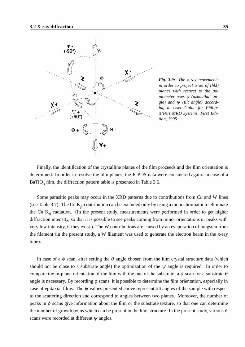
zation. A full description of the texture requires the specification of three angles named θ , φ , and ψ .
Therefore, θ -2θ scan, pole figure and φ scan should be measured (see Fig. 3.9 later).
The film orientation or texture can be determined by measuring a pole figure, which is most
similar to a stereographic projection, and by comparing it with a pole figure of the substrate. Pole
figures show the variation of the diffraction intensity (“pole density”) with pole orientation for a
selected set of crystal planes. If the film grains have a completely random orientation, these poles
will be distributed uniformly over the projection. If a preferred orientation is present, the poles will
tend to cluster in certain areas of the projection, leaving other areas virtually unoccupied. Although
only a pole figure can provide a complete description of the preferred orientation, some information
can be obtained fairly quickly by a comparison of calculated diffraction line intensities with those
observed on an ordinary diffractometer scan. If a sample is examined in the diffractometer by the
usual θ -2θ–scan, then the only grains which can contribute to the hkl reflection are those whose (hkl)
planes are parallel to the substrate surface. If the film texture is such that there are very few such
grains, the intensity of the hkl reflection will be automatically low.
A pole figure analysis involves two rotations about φ and ψ axes. Valuable information with
respect to the crystallographic orientation of a film on a substrate can be obtained by a φ scan taken
at definite θ and ψ values.
The crystallite size can also be measured by diffraction. When the size of the individual crystallites
is less than 100 nm, the term particle size is usually used, but the term crystallite size is more precise.
This size is given by measuring the Full Width at Half Maximum (FWHM) as follows:
FWHM =0:9λtcosθ
(3.3)

3.2 X-ray diffraction 34
where λ is the wavelength, t is the diameter of the crystallites and θ is the diffraction angle. An
efficient method for measuring the size of small crystallites is the so-called “small-angle scattering”
which uses a scattering angle close to 0Æ to observe the size of the film crystallites. The FWHM
values are calculated from the width of a specific peak in the scattered intensity vs. 2θ graph.
The shape of the diffraction peak, i.e., the intensity as a function of the rotation of the sample, is
termed rocking curve. A complete value of FWHM should be calculated from the rocking curve and
compared with the one of the intensity vs. 2θ curve. The presence of linear or planar defects in the
crystalline structure of the sample increases the width of the rocking curve. Measurement of rocking
curves is, therefore, important for assessing the perfection of the structure of epitaxial films.
XRD analysis performed in this study
In this study, crystallographic analyses of BaTiO3 films and BaTiO3/SrTiO3 multilayers deposited
on SrTiO3 substrates by PLD were performed by XRD θ–2θ and φ scans, and by recording pole
figures using a Philips X’Pert MRD four-circle diffractometer with Cu Kα radiation and a parallel
plate collimator in front of the detector achieving a 2θ resolution of 0.1Æ. Pole figures were measured
using an open Eulerian cradle.
The surface normal of the sample can be positioned to coincide with the diffractometer z axis (z
rotation). In addition, using x and y rotations the sample position can be optimized with respect to
the azimuthal angle (φ ) and the tilt angle (ψ), respectively. The data collection software can use the
x and y rotations to adjust the sample position during texture measurements. These five monitorized
rotations are shown in Fig. 3.9. The adjustment of the surface of the sample is extremely important.
A change in the volume of the diffracted material resulting in a change in absorption occurs when the
sample is rotated to different φ or ψ angles.
The following experimental procedure was followed in case of a θ -2θ–scan:
� After loading the sample, the weakest or a weak reflection of the substrate peaks (to minimize
the damage of detector from a strong beam of a single crystal substrate) has been chosen from
the diffraction pattern table according to the Joint Committee on Powder Diffraction Standards
(JCPDS, 1995). In case of SrTiO3, this pattern is presented in Table 3.5. In the measurements
of the present work, the 300 reflection was considered for SrTiO3 (2θ = 72.5Æ).
� The optimization of φ and ψ angles is performed in order to record a strong contribution from
the film. Fixing these two angles, the sample will then be rotated in only one direction by the
variation of the θ angle.
� The measured intensity of a θ–2θ scan was recorded by a computer connected to the diffrac-
tometer.
� The recorded intensity was plotted and analyzed using the PC-APD 4.0 software.
3.2 X-ray diffraction 35
Fig. 3.9: The x-ray movementsin order to project a set of (hkl)planes with respect to the go-niometer axes φ (azimuthal an-gle) and ψ (tilt angle) accord-ing to User Guide for PhilipsX’Pert MRD Systems, First Edi-tion, 1995.
Finally, the identification of the crystalline planes of the film proceeds and the film orientation is
determined. In order to resolve the film planes, the JCPDS data were considered again. In case of a
BaTiO3 film, the diffraction pattern table is presented in Table 3.6.
Some parasitic peaks may occur in the XRD patterns due to contributions from Cu and W lines
(see Table 3.7). The Cu Kβ contribution can be excluded only by using a monochromator to eliminate
the Cu Kβ radiation. (In the present study, measurements were performed in order to get higher
diffraction intensity, so that it is possible to see peaks coming from minor orientations or peaks with
very low intensity, if they exist.). The W contributions are caused by an evaporation of tungsten from
the filament (in the present study, a W filament was used to generate the electron beam in the x-ray
tube).
In case of a φ scan, after setting the θ angle chosen from the film crystal structure data (which
should not be close to a substrate angle) the optimization of the ψ angle is required. In order to
compare the in-plane orientation of the film with the one of the substrate, a φ scan for a substrate θangle is necessary. By recording φ scans, it is possible to determine the film orientation, especially in
case of epitaxial films. The ψ values presented above represent tilt angles of the sample with respect
to the scattering direction and correspond to angles between two planes. Moreover, the number of
peaks in φ scans give information about the film or the substrate texture, so that one can determine
the number of growth twins which can be present in the film structure. In the present study, various φscans were recorded at different ψ angles.

3.2 X-ray diffraction 36
Table 3.5: Selected data on the SrTiO3 (cubic structure - Pm3m symmetry group) diffraction pattern accordingto Swanson and Fuyat, Natl. Bur. Stand., Circular 539, 3, 44 (1954). Intensities are expressed as percentagesof the strongest peak of the pattern.
2θ (degree) X-ray intensity (a.u.) h k l D spacing (Å)22.783 12 1 0 0 3.90032.424 100 1 1 0 2.759039.984 30 1 1 1 2.253046.483 50 2 0 0 1.952052.357 3 2 1 0 1.746057.794 40 2 1 1 1.594067.803 25 2 2 0 1.381072.543 1 3 0 0 1.302077.175 15 3 1 0 1.235081.721 5 3 1 1 1.177486.204 8 2 2 2 1.1273
Although several θ -2θ and φ scans are sufficient in order to determine and to confirm the film
orientation with respect to the substrate orientation, it is rather difficult to determine whether the film
has also other minor orientations, which can not be discriminated in a θ -2θ scan (e.g., because of
a relatively weak peak intensity or because of an overlapping of film peaks with substrate peaks).
Therefore, it is necessary to record φ scans at all ψ angles (from 0 to 90Æ). The result is a pole figure
at a certain 2θ angle providing a chance to see other possible orientations and also to confirm the film
orientation which was determined previously by recording the θ -2θ scan.
During the pole figure measurement, the θ angle is fixed for a chosen direction of the film crystal,
and angles φ and ψ are varied. All pole figures were plotted with the pole distance angle from ψ =
0Æ (center) to ψ = 90Æ (rim). ψ = 90Æ corresponds to the substrate surface being parallel to the plane
defined by the incident and reflected x-ray beams.
The FWHM values of the film used in the present study were calculated from both rocking curves
and φ -scan curves, comparing them with the FWHM of the substrate in order to evaluate the crys-
tallinity and the in-plane alignment, respectively. This gives information about the “mozaicity” of the
film.

3.2 X-ray diffraction 37
Table 3.6: Selected data on the BaTiO3 (tetragonal structure - P4mm symmetry group) diffraction patternaccording to Swanson and Fuyat, Natl. Bur. Stand., Circular 539, 3, 45 (1954). Intensities are expressed aspercentages of the strongest peak of the pattern.
2θ (degree) X-ray intensity (a.u.) h k l D spacing (Å)22.038 12 0 0 1 4.03022.262 25 1 1 0 3.99031.497 100 1 0 1 2.83831.646 100 1 1 0 2.82538.887 46 1 1 1 2.31444.855 12 0 0 2 2.01945.377 37 2 0 0 1.99750.613 6 1 0 2 1.80250.976 8 2 0 1 1.79051.099 7 2 1 0 1.78655.953 15 1 1 2 1.64256.251 35 2 1 1 1.63465.753 12 2 0 2 1.41966.121 10 2 2 0 1.41270.357 5 2 1 2 1.33770.661 2 3 0 0 1.33274.334 5 1 0 3 1.27575.092 7 3 0 1 1.26475.162 9 3 1 0 1.26378.765 3 1 1 3 1.21479.470 5 3 1 1 1.20583.490 7 2 2 2 1.156986.963 1 2 0 3 1.119487.385 1 [3 0 2] 1.116188.066 1 3 2 0 1.1082
Table 3.7: X-ray K-level emission lines of Cu and W according to ref. [136].
Element Energy Kα1 Kα2 Kβ Lα1
(keV) very strong strong weakCu 8.04 1.540562 1.544390 1.392218 13.336W 58.87 0.20901 0.213828 0.184374 1.47639
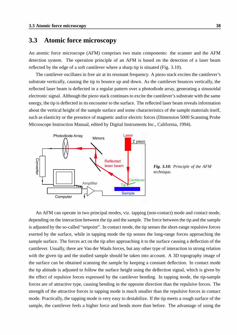
3.3 Atomic force microscopy 38
3.3 Atomic force microscopy
An atomic force microscope (AFM) comprises two main components: the scanner and the AFM
detection system. The operation principle of an AFM is based on the detection of a laser beam
reflected by the edge of a soft cantilever where a sharp tip is situated (Fig. 3.10).
The cantilever oscillates in free air at its resonant frequency. A piezo stack excites the cantilever’s
substrate vertically, causing the tip to bounce up and down. As the cantilever bounces vertically, the
reflected laser beam is deflected in a regular pattern over a photodiode array, generating a sinusoidal
electronic signal. Although the piezo stack continues to excite the cantilever’s substrate with the same
energy, the tip is deflected in its encounter to the surface. The reflected laser beam reveals information
about the vertical height of the sample surface and some characteristics of the sample materials itself,
such as elasticity or the presence of magnetic and/or electric forces (Dimension 5000 Scanning Probe
Microscope Instruction Manual, edited by Digital Instruments Inc., California, 1994).
Fig. 3.10: Principle of the AFMtechnique.
An AFM can operate in two principal modes, viz. tapping (non-contact) mode and contact mode,
depending on the interaction between the tip and the sample. The force between the tip and the sample
is adjusted by the so-called “setpoint”. In contact mode, the tip senses the short-range repulsive forces
exerted by the surface, while in tapping mode the tip senses the long-range forces approaching the
sample surface. The forces act on the tip after approaching it to the surface causing a deflection of the
cantilever. Usually, there are Van der Waals forces, but any other type of interaction in strong relation
with the given tip and the studied sample should be taken into account. A 3D topography image of
the surface can be obtained scanning the sample by keeping a constant deflection. In contact mode
the tip altitude is adjusted to follow the surface height using the deflection signal, which is given by
the effect of repulsive forces expressed by the cantilever bending. In tapping mode, the tip-sample
forces are of attractive type, causing bending in the opposite direction than the repulsive forces. The
strength of the attractive forces in tapping mode is much smaller than the repulsive forces in contact
mode. Practically, the tapping mode is very easy to destabilize. If the tip meets a rough surface of the
sample, the cantilever feels a higher force and bends more than before. The advantage of using the
3.4 Transmission electron microscopy 39
tapping mode is due to the well-known fact that the sample surface state is not modified, while the
contact mode is used nowadays to add or remove atoms from or to the sample surface. There is also
a preference in using the tapping mode in order to record images of better resolution.
In this study, the surfaces of substrates and deposited films were studied by a Digital Instruments
5000 microscope working in tapping mode and using ultrasharp silicon tips. The tip characteristics
are: height between 15 and 20 µm, average resonance frequency about 350 kHz, typical force constant
40 N/m, according to the producer specifications (Silicon-MDT in cooperation with the MikroMasch
company). These tips have a pyramidal shape with a radius of curvature less than 10 nm, and the full
tip cone angle is less than 20Æ.
The surface roughness measured by AFM depends on the surface area, and the variation in height
of the sample surface.
The root-mean-square-roughness (RMS) is defined as follows:
RMS ==
s1N
N
∑i=1
(Zi�Zaverage)2 (3.4)
where Zaverage is the average value of the height (Z) values within the respective area, Zi is the point
height value and N is the number of points within the given area.
Some other roughness measures are considered by the AFM software, e.g. the maximum height
of a given area which is calculated as the difference in height between the highest and the lowest point
of the respective area.
It should be noted that the AFM images shown in the present study have been converted to planar
images by “planefitting”or “flattening” (by fitting by a polynomial function with a selected order2
each scan line of data which compose the final image). Then the polynomial component is subtracted
from the scan line. This process is repeated for each scan line in the image eliminating the unwanted
features from the scan lines, e.g. horizontal bands or image bow. The final image is a well-seen
image, while the as-measured image shows a great contrast in black and white making the image not
well visible. In order to give the reader the true values, all the RMS values presented in this paper are
obtained for the as-measured images, even if they are included in figures together with planar images.
3.4 Transmission electron microscopy
Microstructure analysis of the interface between the BaTiO3 film and the SrTiO3 substrate, or between
different layers of BaTiO3/SrTiO3 multilayers was performed by cross-sectional high-resolution trans-
mission electron microscopy (HRTEM). A JEOL 4010 electron microscope at a primary beam energy
of 400 keV was used to study the interfaces.
2In the present study, only the first order of the polynomial function was consistently used. In this way, a first orderleast-square-fit was calculated for the selected area, then it was subtracted from each scan line of the final image preservingthe image from the tall features in predominantly flat areas.

3.5 Electrical measurements 40
Specimen preparation
In order to analyze the BaTiO3 film deposited on a SrTiO3 substrate by cross-section, specimens of
these samples are prepared by polishing and ion milling techniques. The sample is cut into thin slices
normal to the interfaces which are glued face-to-face. Then this sandwich is glued between two spac-
ers which are usually pieces of SrTiO3 substrates because they should have the same hardness. The
whole sandwich is polished manually until the total width is about 100 µm. The specimen is then
glued to a metallic grid. The next step is to thin the specimen by further dimple grinding. The spec-
imen is then dimple-polished keeping a fixed radius of curvature in the center. A great advantage of
this process is that one can control the thickness of the removed material by the depth of the dimple
and interrupt the polishing when it is necessary, preventing specimen damage. Dimple-grinding both
sides of the sandwich-specimen, the probability of a final perforation in the center increases. There-
fore, it is preferably to polish one side and preserve the other. The final step consists of ion milling
which involves bombarding the thin specimen using energetic Ar ions and remove material by sput-
tering until the film is thin enough to be observed in TEM. However, some implantation occurs so that
the near-surface chemistry is changed. Therefore, the top layer becomes often amorphous. First, a
rapid ion thinning is performed for about 2 h. After a careful investigation of the sample by an optical
microscope, the last step consists of a fine polish for 4 - 7 s at 10Æ angle with respect to the surface
(inclination helps to minimize the penetration of the ion beam) using an accelerating voltage of 2 - 4
keV. This step completes the cross-section specimen preparation for TEM investigation.
3.5 Electrical measurements
Pt top-electrodes with 100 nm thickness and 0.15 mm diameter were deposited by 5 min rf-sputtering
through a metallic mask at 40 W power in an Ar atmosphere at room temperature. The sputtering
machine uses a CESAR 133 rf-generator with a maximum frequency of 13.56 MHz and a maximum
power of 300 W. Optimum power is adjusted by two variable tuning capacitors called Load (CL)
and Tune (CT ). In order to observe the possible fluctuations in reflected power, pre-sputtering was
performed for 15 min prior to each deposition, keeping the reflected power around 1 W.
Electrical characterization was performed using a TF Analyzer 2000 ferroelectric tester (Aix-
ACCT) and a Hewlett Packard HP 4195A Impedance/Gain-phase analyzer. C–V measurements were
performed applying an ac signal with an amplitude of 10 mV at 1 MHz, while a dc bias was swept
at a rate of 0.2 V/s from 0 to Vmax and vice-versa with a delay time of 0.5 s. The maximum ap-
plied dc current/voltage is � 20 mA/� 40 V. Capacitance values were extracted from the measured
absolute values of the impedance with an accuracy of 0.1% and a resolution of 4 1/2 digits. The mea-
sured capacitance was recorded applying a voltage ranging from negative values to positive values.
The measured impedance values are calculated from the equivalent series circuit [R + jX or (R2 +
X2)1=2], where R is the resistance and X is the reactance. The residual impedance was measured at 1

3.5 Electrical measurements 41
MHz. This value was then stored and used as offset data for subsequent measurements. The ambient
temperature was considered equal to 23 ÆC.