2-bit reconfigurable unit-cell and electronically
TRANSCRIPT
HAL Id: hal-02516789https://hal-univ-rennes1.archives-ouvertes.fr/hal-02516789
Submitted on 24 Mar 2020
HAL is a multi-disciplinary open accessarchive for the deposit and dissemination of sci-entific research documents, whether they are pub-lished or not. The documents may come fromteaching and research institutions in France orabroad, or from public or private research centers.
L’archive ouverte pluridisciplinaire HAL, estdestinée au dépôt et à la diffusion de documentsscientifiques de niveau recherche, publiés ou non,émanant des établissements d’enseignement et derecherche français ou étrangers, des laboratoirespublics ou privés.
2-Bit Reconfigurable Unit-Cell and ElectronicallySteerable Transmitarray at Ka-Band
Fatimata Diaby, Antonio Clemente, Ronan Sauleau, Kien Pham, LaurentDussopt
To cite this version:Fatimata Diaby, Antonio Clemente, Ronan Sauleau, Kien Pham, Laurent Dussopt. 2-Bit Recon-figurable Unit-Cell and Electronically Steerable Transmitarray at Ka-Band. IEEE Transactions onAntennas and Propagation, Institute of Electrical and Electronics Engineers, 2020, 68 (6), pp.5003-5008. �10.1109/TAP.2019.2955655�. �hal-02516789�

Abstract—This paper presents the design, optimization, fabrication, and
characterization of an electronically steerable transmitarray with 2 bits of
phase quantization per unit cell. The proposed transmitarray operates in
linear polarization at Ka-band and is composed of 14×14 reconfigurable
unit-cells. Four p-i-n diodes are integrated on each unit-cell to control the
radiated field phase distribution across the transmitarray aperture. The
prototype demonstrates experimentally pencil beam scanning over a
120×120-degree window, a maximum gain at broadside of 19.8 dBi, and a
3-dB fractional bandwidth of 16.2%.
Index Terms—Transmitarray antennas, beam steering, beam forming,
Ka-band, discrete lens, electronically steerable antenna.
I. INTRODUCTION
The demonstration of relatively low-cost and innovative antenna
technologies for user terminals with electronically beam-steering
capabilities is a key element in the development of the future Internet
of Space (IoS) ecosystem [1]. This innovative communication network
will deliver high data-rate services to every part of the globe thanks to
future-generation terrestrial and broadband satellite networks.
Satellite constellations operating at Ka-band play a fundamental
role to increase the system bandwidth and consequently the achievable
data rate; the allocated frequency bands for both military and civil
applications are 17.7 – 21.2 GHz and 27.5 – 31.0 GHz, for the
downlink and uplink respectively. In the last years, several antenna
configurations based on fully mechanical (e.g. [2],[3]), hybrid
electromechanical (e.g. [4]), and electronically steerable (e.g. [5]-[7])
architectures have been presented as academic or industrial solutions.
The existing fully electronically reconfigurable architectures are based
on liquid crystal controlled holographic metasurfaces [5],[6] or more
importantly on classical phased arrays, e.g. [7].
For the future 5th Generation mobile terrestrial networks, several
frequency ranges (24.27 – 27.5 GHz, 31.8 – 33.4 GHz, or 37.0 – 40.5
GHz) at Ka-band have been indicated as potential candidates for the
development of high performance backhauling and access point
systems [8]. In the last years, several phased array solutions [9] have
been proposed and are generally based on analogue [10] or fully-digital
architectures [11].
Thanks to their spatial feeding architecture and the possibility to
control easily the phase distribution on the array aperture,
transmitarrays (TAs) and reflectarrays are excellent alternatives for
beam steerable applications. In contrast to reflectarrays, TAs do not
suffer from any feed blockage. Moreover, advanced TA designs may
lead to ultra-low profile architectures [12]-[13] and to a full control of
the transmission phase and polarization at the same time [14]. A TA is
typically composed of one or several focal sources illuminating an
Manuscript received December 19, 2018, revised July 30, 2019, accepted November 17, 2019. This work was supported by the National Research
Agency through the project “TRANSMIL” under Grant ANR-14-CE28-0023.
F. Diaby, A. Clemente, and L. Dussopt are with CEA-LETI, Minatec Campus, F38054 Grenoble, France (e-mail: [email protected]).
array of unit-cells (flat lens). Each unit-cell consists of a first antenna
array working in receive mode and connected (through phase shifters)
to a second array working in transmission mode.
Several wideband fixed- [14]-[15] or switched-beam [16], and
electronically-reconfigurable TAs [12],[13],[17]-[20] have been
presented and demonstrated in the literature up to sub-THz frequencies
[21]. In our previous works [12],[18], the possibility to implement
electronic beam-scanning has been successfully shown using 1-bit
reconfigurable TAs with 800 p-i-n diodes integrated on the antenna
aperture. Shaped beams (e.g. flat-top patterns) have also been
demonstrated [18]. One-bit architectures are relatively low cost, low
loss, and wideband (3-dB gain bandwidth up to 15%) due to reduced
number of layers and solid-state devices integrated to control the
transmission phase. However, the limited phase resolution leads to
directivity loss (close to 4 dB for a 400-element antenna) and high side
lobes. Two-bit phase quantization can be used to increase both aperture
efficiency and radiation pattern quality at the cost of a higher
complexity and optimization constraints.
Here a 2-bit electronically-reconfigurable TA prototype is presented
at Ka-band. The proposed antenna is based on the reconfigurable unit-
cell architecture previously reported in our preliminary conference
works [22],[23]. To the best of our knowledge, the TA prototype
described here is one of the largest (14×14 unit-cells) 2-bit
electronically-reconfigurable TA presented in the open literature at
Ka-band, and its radiation efficiency is among the highest reported so
far (around 48%). The only 2-bit prototype previously introduced in
[17] contains 22×22 unit-cells, but the radiation characteristics
demonstrated experimentally were degraded by the low reliability of
the MEMS technology used (about 8 dB gain reduction).
This paper is organized as follows. The architectures of the
proposed 2-bit electronically reconfigurable unit-cell and TA and the
fabricated prototypes are presented in Section II. Then, we describe in
Section III the radiation performance obtained in simulations and
measurements. Finally, conclusion are drawn in Section IV.
II. TRANSMITARRAY ARCHITECTURE, DESIGN AND FABRICATION
A. 2-Bit Reconfigurable Unit-Cell: Design, Fabrication and
Experimental Characterization
The global architecture, details on geometrical parameters,
operation principle, and numerical analysis of the 2-bit reconfigurable
unit-cell have been described and discussed in [22],[23]. Standard
Printed Circuit Board (PCB) process, i.e. with minimum trace width of
80 µm and minimum via-diameter of 120 µm, has been selected to
demonstrate the possibility to implement the proposed design by using
mature and relatively low cost fabrication technologies. This unit-cell
R. Sauleau is with Univ Rennes, CNRS, IETR (Institut d’Électronique et de Télécommunications de Rennes), UMR 6164, F-35000 Rennes, France (e-mail:
K. T. Pham was with Univ Rennes, CNRS, IETR (Institut d’Électronique et de Télécommunications de Rennes), UMR 6164, F-35000 Rennes, France. He
is now with International Univ. VNU-HCM, Ho Chi Minh City, Vietnam.
2-Bit Reconfigurable Unit-Cell and Electronically Steerable
Transmitarray at Ka-Band
Fatimata Diaby, Antonio Clemente, Senior Member, IEEE, Ronan Sauleau, Fellow, IEEE, Kien T.
Pham, Member, IEEE, and Laurent Dussopt, Senior Member, IEEE
Accep
tedMan
uscri
pt
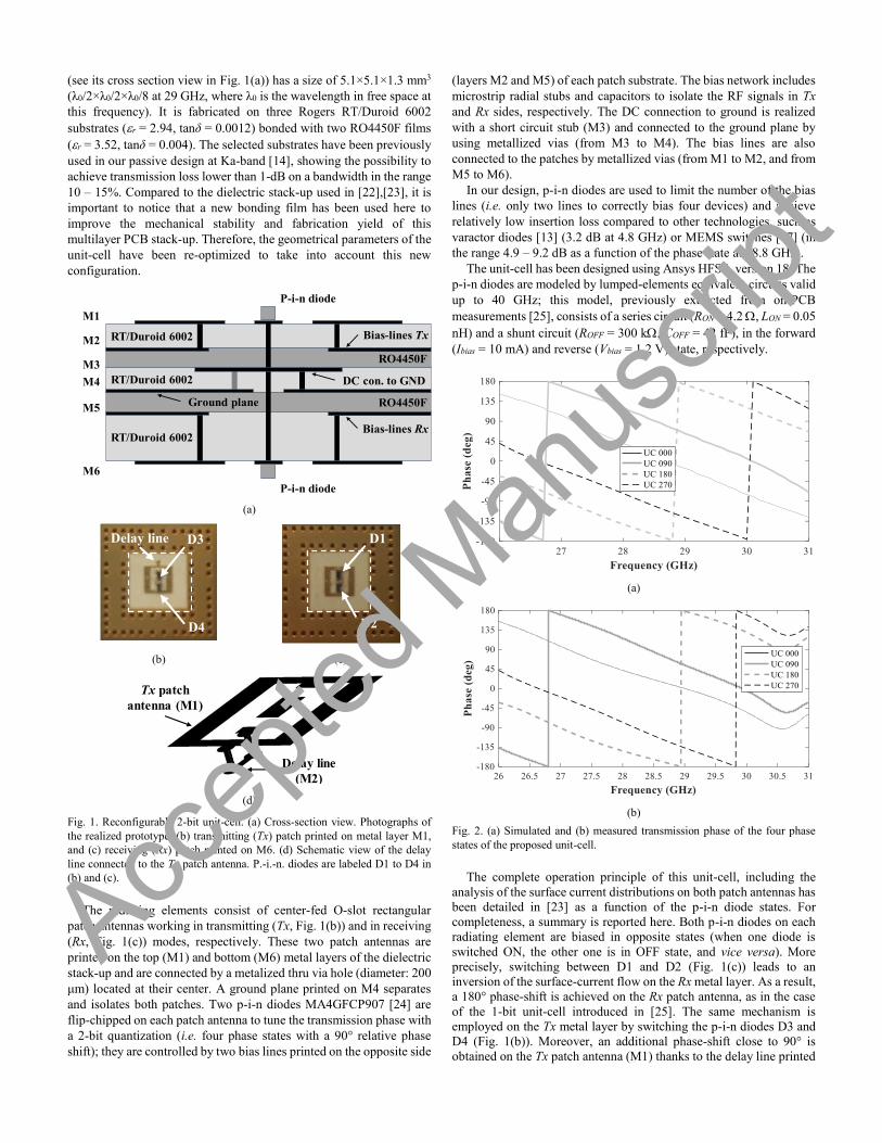
(see its cross section view in Fig. 1(a)) has a size of 5.1×5.1×1.3 mm3
(λ0/2×λ0/2×λ0/8 at 29 GHz, where λ0 is the wavelength in free space at
this frequency). It is fabricated on three Rogers RT/Duroid 6002
substrates (r = 2.94, tanδ = 0.0012) bonded with two RO4450F films
(r = 3.52, tanδ = 0.004). The selected substrates have been previously
used in our passive design at Ka-band [14], showing the possibility to
achieve transmission loss lower than 1-dB on a bandwidth in the range
10 – 15%. Compared to the dielectric stack-up used in [22],[23], it is
important to notice that a new bonding film has been used here to
improve the mechanical stability and fabrication yield of this
multilayer PCB stack-up. Therefore, the geometrical parameters of the
unit-cell have been re-optimized to take into account this new
configuration.
(a)
(b) (c)
(d)
Fig. 1. Reconfigurable 2-bit unit-cell. (a) Cross-section view. Photographs of
the realized prototype: (b) transmitting (Tx) patch printed on metal layer M1,
and (c) receiving (Rx) patch printed on M6. (d) Schematic view of the delay
line connected to the Tx patch antenna. P.-i.-n. diodes are labeled D1 to D4 in
(b) and (c).
The radiating elements consist of center-fed O-slot rectangular
patch antennas working in transmitting (Tx, Fig. 1(b)) and in receiving
(Rx, Fig. 1(c)) modes, respectively. These two patch antennas are
printed on the top (M1) and bottom (M6) metal layers of the dielectric
stack-up and are connected by a metalized thru via hole (diameter: 200
μm) located at their center. A ground plane printed on M4 separates
and isolates both patches. Two p-i-n diodes MA4GFCP907 [24] are
flip-chipped on each patch antenna to tune the transmission phase with
a 2-bit quantization (i.e. four phase states with a 90° relative phase
shift); they are controlled by two bias lines printed on the opposite side
(layers M2 and M5) of each patch substrate. The bias network includes
microstrip radial stubs and capacitors to isolate the RF signals in Tx
and Rx sides, respectively. The DC connection to ground is realized
with a short circuit stub (M3) and connected to the ground plane by
using metallized vias (from M3 to M4). The bias lines are also
connected to the patches by metallized vias (from M1 to M2, and from
M5 to M6).
In our design, p-i-n diodes are used to limit the number of the bias
lines (i.e. only two lines to correctly bias four devices) and achieve
relatively low insertion loss compared to other technologies, such as
varactor diodes [13] (3.2 dB at 4.8 GHz) or MEMS switches [17] (in
the range 4.9 – 9.2 dB as a function of the phase state at 38.8 GHz).
The unit-cell has been designed using Ansys HFSS, version 18. The
p-i-n diodes are modeled by lumped-elements equivalent circuits valid
up to 40 GHz; this model, previously extracted from on-PCB
measurements [25], consists of a series circuit (RON = 4.2 , LON = 0.05
nH) and a shunt circuit (ROFF = 300 k, COFF = 42 fF), in the forward
(Ibias = 10 mA) and reverse (Vbias = 1.2 V) state, respectively.
(a)
(b)
Fig. 2. (a) Simulated and (b) measured transmission phase of the four phase
states of the proposed unit-cell.
The complete operation principle of this unit-cell, including the
analysis of the surface current distributions on both patch antennas has
been detailed in [23] as a function of the p-i-n diode states. For
completeness, a summary is reported here. Both p-i-n diodes on each
radiating element are biased in opposite states (when one diode is
switched ON, the other one is in OFF state, and vice versa). More
precisely, switching between D1 and D2 (Fig. 1(c)) leads to an
inversion of the surface-current flow on the Rx metal layer. As a result,
a 180° phase-shift is achieved on the Rx patch antenna, as in the case
of the 1-bit unit-cell introduced in [25]. The same mechanism is
employed on the Tx metal layer by switching the p-i-n diodes D3 and
D4 (Fig. 1(b)). Moreover, an additional phase-shift close to 90° is
obtained on the Tx patch antenna (M1) thanks to the delay line printed
RT/Duroid 6002
RT/Duroid 6002
RT/Duroid 6002
RO4450F
RO4450F
P-i-n diode
P-i-n diode
M1
M2
M3
M4
M5
M6
Bias-lines Rx
Bias-lines Tx
Ground plane
DC con. to GND
D3
D4
Delay line D1
D2
Tx patch
antenna (M1)
Delay line
(M2)
Accep
ted M
anus
cript

on M2 (Fig. 1(d)) and connected to the rectangular patch (M1). As a
result, four phase states are obtained: 0°, 90°, 180° and 270°.
The fabricated unit-cell (labelled UC000, UC090, UC180, and
UC270) has been characterized using the waveguide simulator
described in [25] (i.e. two rectangular waveguides WR-28 and two
rectangular-to-square waveguide transitions). As shown in Fig. 1(b)-
(c), two rings of vias and a large ground plane are used to guarantee a
good electrical contact between the waveguide flanges and the unit-
cell prototypes. Furthermore, the simulated results have been obtained
by modeling the waveguide setup used experimentally. The simulated
3-dB absolute transmission bandwidth (BW) is equal to 9.6%, 16.5%,
12.1% and 15.5% for UC000, UC090, UC180, and UC270,
respectively. They are in acceptable agreement with the measured
values (11.7%, 10.1%, 12.1%, and 10.3%, respectively).
The simulated and measured transmission phase of the unit-cell is
plotted in Fig. 2 for the four phase-states. The measured relative phase-
shift between the UC000 state and the three other states (UC090,
UC180, and UC270) is equal to 124°, 178°, and 315° at 29 GHz,
respectively (in simulation, these values are equal to 105.9°, 178.5°,
and 297.6°). The relative phase shift between UC000 and UC180, and
between UC090 and UC270, is very stable and nearly equal to 180°
over the full unit-cell transmission bandwidth; this comes from the
switching mechanism of each pair of diodes, as described above. This
result is in agreement with our previous demonstrations [25].
Moreover, the non-perfect 90° phase-shift at central frequency
between UC000 and UC090, and between UC180 and UC270, is due
to the complexity of the optimization and to the standard PCB
fabrication constraints considered in the design.
The differences between the simulated and measured results are
most probably due to the misalignment of the unit-cell in the
waveguide setup and to the PCB fabrication errors (layer
misalignments, geometrical dimensions, non-uniform thickness of the
bonding film layers due to the pressing process, etc.). These statements
have been confirmed by retro-simulations, but the detailed
presentation of the results is out of the scope of this paper. The
insertion loss measured and simulated at 29 GHz and the 3-dB
transmission bandwidth of the unit-cell in the four phase-states are
summarized in Table I.
TABLE I
MEASURED AND SIMULATED PERFORMANCE OF THE 2-BIT UNIT-CELL
Transm. loss at
29 GHz (dB) 3-dB transm. BW
(GHz) Phase shift at 29
GHz (deg.)
Sim. Meas. Sim. Meas. Sim. Meas.
UC000 1.0 2.1 27.0 – 30.1
26.8 – 30.2
- -
UC090 0.8 1.5 27.4 – 31.0
27.4 – 30.3
105.9 124.0
UC180 1.0 2.3 26.8 – 30.5
26.7 – 30.2
178.5 178.0
UC270 0.8 1.6 27.5 – 31.3
27.3 – 30.3
297.6 315.0
B. Transmitarray Design and Fabrication
The fabricated 14×14-element TA is shown in Fig. 3. The aperture
size has been chosen to achieve similar performance (i.e. gain in the
range of 20 – 23 dBi) if compared to the one of our previous works at
Ka-band [12]. The flat panel (142×163 mm²) is realized on the same
dielectric stack-up as for the unit-cell (Fig. 1(a)). It includes the
radiating aperture of size 71.4×71.4 mm² (7λ0×7λ0), the 784 p-i-n
diodes integrated on the receiving (Fig. 3(a)-(b)) and transmitting
layers (Fig. 3(c)-(d)), the DC bias network, and the board-to-board
connectors used to interconnect the steering logic. The focal source is
a linearly-polarized pyramidal standard gain horn antenna with a
nominal gain of 10-dBi. The focal distance is fixed to 48 mm (F/D =
0.67) and has been optimized with our in-house tool in order to
maximize the aperture efficiency.
C. Bias Network Design and Impact on the Unit-Cell Performance
The fabricated TA is divided into four 7×7 subarrays to bias the 784
integrated p-i-n diodes. Each steering-logic board drives one subarray
with two ±10 mA bias currents (one for diodes D1 and D2, and one for
D3 and D4) per unit-cell. Considering the p-i-n diode threshold voltage
(1.2 V), the total power consumption is 24 mW for each unit-cell and
4.7 W for the full array.
(a) (b)
(c) (d)
(e)
Fig. 3. Photographs of the realized electronically steerable transmitarray, (a)-
(b) receiving and (c)-(d) transmitting layers with p-i-n diodes. (e) Schematic
view of the bias network on one line of the 7×7 subarray.
Radiating aperture
M1
M2
M6
M5Accep
ted M
anus
cript
The bias lines arrangement is realized by symmetries in both
receiving and transmission subarray sides. A total number of 98 bias
lines (i.e. two lines per unit-cell) is necessary to bias the 196 p-i-n
diodes located on the transmitting and receiving layers of each
subarray. The photographs of the TA receiving (M1) and transmitting
(M6) layers with their bias line distribution network are shown in Fig.
3(a)-(b) and (c)-(d), respectively. This bias line arrangement is
identical for each of the four subarrays. As presented in Fig. 3(e), the
bias lines of the transmitting patch diodes are distributed between the
layers M1 (5 lines) and M2 (2 lines). On the receiving side, the 7 bias
lines have been distributed on layers M5 (5 lines) and M6 (2 lines).
In the proposed analysis, three unit-cell configurations with 2, 6,
and 14 DC bias lines have been considered to study the impact of the
bias network on the unit-cell frequency response. These three
configurations are considered as representative test cases. In the first
case, the bias lines controlling the p-i-n diodes soldered on the patch
antennas on M1 and M6 are printed on M2 and M5, respectively, as
described in the Section II.A. Furthermore, for the configuration with
14 lines, the bias lines are distributed on metallic layers M1, M2, M5
and M6.
These three unit-cell configurations have been simulated with HFSS
for the four phase states with periodic conditions and Floquet mode
excitation under normal incidence. For brevity purposes, we provide
here only experimental results obtained for phase state UC000. The
corresponding results (measured amplitude and phase in transmission)
are plotted in Fig. 4. The obtained results show very stable scattering
parameters in all cases, demonstrating thereby that the DC bias lines
do not impact the RF performance, as previously shown in [12],[18].
The impact of the oblique incidence has also been investigated, but the
results are not detailed here because the conclusions are the same of
the one presented in [18].
Fig. 4. Measured (a) amplitude and (b) phase of the transmission coefficient of
cell UC000 as a function of the frequency and the number of bias lines.
III. BEAM COLLIMATING AND SCANNING: NUMERICAL AND
EXPERIMENTAL RESULTS
The radiation characteristics of the proposed TA have been
computed using our hybrid in-house tool based on analytical equations
and full-wave simulations of the unit-cells and focal sources.
Measurements have been carried out in the CEA-Leti far-field
anechoic chamber.
The theoretical directivity of the uniform 7λ0×7λ0 radiating aperture
is equal to 27.9 dBi. This value has been used to compute the TA
aperture efficiency.
A. Performance at Broadside
The theoretical (in-house tool), simulated (Ansys HFSS) and
measured gain at broadside is plotted in Fig. 5 as a function of
frequency. The theoretical and simulated results, indicated as
‘Nominal’ in this Figure, are in a relatively good agreement, with a
maximum difference of 1 dB. The theoretical and measured 3 dB gain
fractional bandwidths are equal to 14.8% (26.7-31 GHz) and 16.2%
(26.2-30.9 GHz) at 29 GHz, respectively. However, significant
discrepancies (around 3.4 dB at 29 GHz) have been obtained when
comparing simulations and measurements (measured gain: 19.8 dBi,
theoretical gain: 23.2 dBi).
Fig. 5. Theoretical, simulated, and measured broadside gain of the TA prototype
as a function of frequency.
(a)
(b)
Fig. 6. Radiation characteristics at broadside. (a) Measured and theoretical gain
radiation patterns at 29 GHz in E (left) and (right) H planes. (b) Measured gain
as a function of frequency and elevation angle in H plane.
To better understand the reasons for these discrepancies, the in-
depth diagnostic of the realized prototype has shown that 51 unit-cells
were found faulty, most probably due to fabrication defaults in the
PCB. DC short circuits between some bias lines and the ground plane
have been detected (e.g. short circuits between metal layers M2-M3
and M4-M5 most probably generated locally during the PCB pressing
and bonding process). The corresponding diodes are thus in the OFF
Accep
ted M
anus
cript

state. The theoretical and simulated frequency responses, indicated as
‘w Faulty UCs’, are plotted and compared to measurements and
nominal simulations in Fig. 5. They are now in much better agreement
with the measurement results, with a maximum gain difference of 0.7
dB at 29 GHz between theory and measurements.
The measured and theoretical gain radiation patterns are plotted and
compared in Fig. 6(a) at 29 GHz. It is important to notice that the
theoretical results have been calculated by considering in the
simulation with the in-hose tool the faulty unit-cells. A very
satisfactory agreement is obtained for the main lobe in both E and H
planes. However, discrepancies on side lobes are observed due to the
spill-over and diffraction effects, which are not taken into account in
the in-house theoretical model. The H-plane radiation patterns
measured from 26 to 31 GHz confirms the wide band properties of the
antenna (Fig. 6(b)).
Fig. 7. Scanning radiation characteristics: measured and theoretical gain
radiation patterns at 29 GHz in H plane for a steering angle of 20° (left) and 40°
(right).
(a)
(b)
Fig. 8. Measured radiation patterns (realized gain) at 29 GHz as a function of
the steering angle. Co-polarization components in (a) E and (b) H planes.
B. Beam Scanning Performance
The beam scanning capabilities of the proposed transmitarray have
been measured for steering angles between -60° and +60° both in E
and H planes.
Fig. 7 represents the measured and theoretical radiation patterns at
29 GHz for an antenna beam pointing at 20° and 40° in H-plane.
Experimentally, the corresponding antenna gain reaches 18.7 and 17.4
dBi, respectively. These values are in good agreement with the theory,
with a peak gain difference lower than 1 dB. Similar results have been
obtained for the other steering angles and H-plane beams.
The scanning capabilities of the antenna are characterized up to 60°
in E- and H-planes in Fig. 10(a)-(b). The scan loss at ±60° reaches
about 5 dB due to the gain variation of the unit-cell radiation pattern
for the same angular range. The slight asymmetry and distortion of the
radiation patterns are due to the faulty unit-cells. It is important to
notice that symmetrical and non-distorted patterns have been obtained
in simulations when the nominal transmitarray configuration without
faulty unit-cells is considered. The cross-polarization discrimination is
also excellent, with a maximum cross-polarization level lower than 4
dBi between -60° and +60°.
In order to highlight the impact of the 51 faulty unit-cells on the
radiation performance of the proposed antenna, the theoretical co-
polarization gain patterns have been plotted in Fig. 9. These patterns
have been computed at broadside and for different scanning angles in
the vertical, horizontal and diagonal planes, when the nominal layout
of the transmitarray without faulty unit-cells is considered. These
results demonstrate an excellent scanning capability up to 60° and
confirm that the pattern asymmetry and distortions are due to the faulty
unit-cells.
Finally, the obtained results of the 2-bit electronically steerable
transmitarray antenna are summarized and compared to the current
state-of-the-art in Table II. As discussed in the Section I, only two
prototypes [12],[17] have been done previously at Ka-band. Both
prototypes demonstrate an aperture efficiency lower than the one
achieved in this work.
(a) (b)
(c) (d)
Fig. 9. Theoretical 2-D gain radiation patterns (Ludwig 3 co-polarization
component) of the 2-bit steerable transmitarray achieved at 29 GHz when the
nominal array layout without faulty unit-cells is considered. (a) Broadside, (b)
(θ0,0) = (40°,0°), (c) (θ0,0) = (60°,90°), and (d) (θ0,0) = (60°,45°).
Accep
ted M
anus
cript

IV. CONCLUSIONS
A 2-bit electronically steerable 14×14 element transmitarray has
been presented in detail at Ka-band. The proposed antenna is based on
a reconfigurable unit-cell with 4 p-i-n diodes to control electronically
its transmission phase. Despite some non-operating unit-cells, which
is a positive outcome from the application point of view showing the
graceful degradation of the performance in such operating conditions,
the radiation patterns remain relatively good with moderate side-lobe
levels. It is believed that this work represents a significant progress in
the current state-of-the-art since there is no other example of a 2-bit
active Ka-band transmitarray with such promising results.
The measured aperture efficiency and 3-dB gain fractional
bandwidth are equal to 15.9% (35% in simulation) and 16.2% at 29
GHz, respectively.
TABLE II
PERFORMANCE COMPARISON WITH EXISTING ELECTRONICALLY STEERABLE
TRANSMITARRAYS
Reference [13] [18] [12] [17] This
work
Layers 7 4 4 3 6
Phase
shifters
Varactor
diodes
p-i-n
diodes
p-i-n
diodes MEMS
p-i-n
diodes
Freq. (GHz) 4.8 9.8 29.0 34.8 29.0
Polarization LP LP CP LP LP
F/D 0.3 0.7 0.6 - 0.67
Phase
resolution 400° 1-bit 1-bit 2-bit 2-bit
Gain (dBi) 15.6 22.7 20.8 9.2 19.8
Ap. eff. (%) 34.0 16.0 9.5 6.2 15.9
3-dB BW
(%)
9% (2-
dB BW) 15.8 14.6 - 16.2
Beam
scanning
capability
±45° E-,
and H-
planes
±40°/±60°
E-, and
H-planes
±60° E-,
and H-
planes
±40° E-,
and H-
planes
±60° E-,
and H-
planes*
* Distortion on the radiation patterns observed for scan angles higher than 40°
are due to the faulty unit-cells.
REFERENCES
[1] S. Raman, R. Weigel, and T. Lee, “The Internet of Space (IoS): a future
backbone for the Internet of Things?,” IEEE Internet of Things Magazine Newsletter, Mar. 8, 2018.
[2] W. W. Milroy, “Continuous transverse stub element devices and methods
of making same,” U.S. Patent 5 266 961, Nov. 30, 1993. [3] M. Ettorre, F. Foglia Manzillo, M. Casaletti, R. Sauleau, L. Le Coq, and
N. Capet, “Continuous transverse stub array for Ka-band applications,”
IEEE Trans. Antennas Propag., vol. 65, no. 12, pp. 7009-7018, Nov. 2015.
[4] B. Tripodi, F. Di Marca, T. Cadili, C. Mollura, F. Di Maggio, and M.
Russo, “Ka-band active phased array antenna system for satellite communications on the move terminal,” in Proc. European Conf.
Antennas Propag. (EuCAP), Rome, Italy, Mar. 2011.
[5] R. A. Stevenson, A. H. Bily, D. Cure, M. Sazegar, and N. Kundtz, “Rethinking wireless communications: advanced antenna design using
LCD technology,” SID Symposium Digest of Technical Papers, vol. 46,
no. 1, pp. 827-830, 2015. [6] Kymeta Website. (2018, Sep.) “mTennaTM and Metamaterials” [Online].
Available: http://www.kymetacorp.com.
[7] I. Wolf, C. Günner, J. Kassner, R. Kulke, and P. Uhlig, “New heights for satellites: LTCC multilayer technology for future satellites,” IEEE
Microwave Magazine, vol. 19, no. 1, pp. 36-47, Jan.-Feb. 2018.
[8] ITU-R, Provisional Final Acts, World Radiocommunication Conference (WRC-15), Nov. 2015.
[9] A. H. Naqvi and S. Lim, “Review of recent phased arrays for millimeter-
wave wireless communication,” Sensors (Basel), vol. 18, 10 3194, Oct. 2018.
[10] K. Kibaroglu, M. Sayginer, and G. M. Rebeiz, “A low-cost scalable 32-
element 28-GHz phase array transceiver for 5G communication links based on a 2 × 2 beamformer flop-chip unit-cell,” IEEE Journal Solid-
States Circuits, vol. 53, no. 5, pp. 1260-1274, May 2018.
[11] B. Yang, Z. Yu, J. Lan, R. Zhang, J. Zhou, and W. Hong, “Digital beamforming-based massive MIMO transceiver for 5G millimeter-wave
communications,” IEEE Trans. Microw. Theory Tech., vol. 66, no. 7, pp.
3403-3418, Jul. 2018. [12] L. Di Palma, A. Clemente, L. Dussopt, R. Sauleau, P. Potier, and P.
Pouliguen, “Circularly-polarized reconfigurable transmitarray in Ka-band
with beam scanning and polarization switching capabilities,” IEEE Trans. Antennas Propag., vol. 65, no. 2, pp. 529-540, Feb. 2017.
[13] J. G. Nicholls and S. V. Hum, “Full-space electronic beam-steering
transmitarray with integrated leaky-wave feed,” IEEE Trans. Antennas Propag., vol. 64, no. 8, pp. 3410-3422, Aug. 2016.
[14] F. Diaby, A. Clemente, K. Pham, R. Sauleau, and L. Dussopt, “Circularly-
polarized transmitarray antennas at Ka-band,” IEEE Antennas Wireless
Propag. Lett., vol. 17, no. 7, pp. 1204-1208, Jul. 2018.
[15] P. Naseri, S. A. Matos, J. R. Costa, and C. A. Fernandes, “Phase-delay
versus phase-rotation cells for circular polarization transmit arrays – application to satellite Ka-band beam steering,” IEEE Trans. Antennas
Propag., vol. 66, no. 3, pp. 1236-1247, Mar. 2018. [16] L. Dussopt, A. Moknache, J. Säily, A. Lamminen, M. Kaunisto, J.
Aurinsalo, T. Bateman, and J. Francey, “A V-band switched-beam
lineraly-polarized transmit-array antenna for wireless backhaul applications,” IEEE Trans. Antennas Propag., vol. 65, no. 12, pp. 6788-
6793, Dec. 2017.
[17] C.-C. Cheng, B. Lakshminarayanan, and A. Abbaspour-Tamijani, “A programmable lens-array antenna with monolithically integrated MEMS
switches,” IEEE Trans. Microw. Theory Tech., vol. 57, no. 8, pp. 1874–
1884, Aug. 2009. [18] A. Clemente, L. Dussopt, R. Sauleau, P. Potier, and P. Pouliguen,
“Wideband 400-element electronically reconfigurable transmitarray in X
Band,” IEEE Trans. Antennas Propag,, vol. 61, no. 10, pp. 5017-5027, Oct. 2013.
[19] C. Huang, W. Pan, and X. Luo, “Low-loss circularly polarized
transmitarray for beam steering application,” IEEE Trans. Antennas Propag., vol. 64, no. 10, pp. 4471-4476, Oct. 2017.
[20] J. R. Reis, R. F. S. Caldeirinh, A. Hammoudeh, and N. Copner,
“Electronically reconfigurable FSS-inspired transmitarray for 2-D beamsteering,” IEEE Trans. Antennas Propag., vol. 65, no. 9, pp. 4880–
4885, Sep. 2017.
[21] Z.-W. Miao, Z.-C. Hao, G. Q. Luo, L. Gao, J. Wang, X. Wang, and W. Hong, “140 GHz high-gain LTCC-integrated transmit-array antenna
using a wideband SIW aperture-coupling phase delay structure,” IEEE
Trans. Antennas Propag., vol. 66, no. 1, pp. 182-190, Jan. 2018. [22] F. Diaby, A. Clemente, L. Di Palma, L. Dussopt, K. Pham, E. Fourn, and
R. Sauleau, “Linearly-polarized electronically reconfigurable
transmitarray antenna with 2-bit phase resolution in Ka-band,” in Proc. Int. Conf. Electromagnetics Advanced Applications (ICEAA 2017),
Verona, Italy, 11-15 Sep. 2017.
[23] F. Diaby, A. Clemente, L. Di Palma, L. Dussopt, K. Pham, E. Fourn, and R. Sauleau, “Design of a 2-bit unit-cell for electronically reconfigurable
transmitarrays at Ka-band,” in Proc. 47th European Microwave
Conference (EuMW 2017), Nuremberg, Germany, 10-12, Oct. 2017, pp. 1321-1324.
[24] MACOM technologies, www.macom.com.
[25] L. Di Palma, A. Clemente, L. Dussopt, R. Sauleau, P. Potier, and P. Pouliguen, “1-bit reconfigurable unit-cell for Ka-band transmitarrays,”
IEEE Antennas Wireless Propag. Lett, vol. 15, pp. 560-563, 2016. Accep
ted M
anus
cript