1/4-inch vga cmos digital image sensor
TRANSCRIPT

MT9V011 - 1/4-Inch VGA Digital Image SensorFeatures
Preliminary‡
1/4-Inch VGA CMOS Digital Image Sensor
Part Number: MT9V011P11STC:BFor the latest data sheet revision, please refer to Micron’s Web site: www.micron.com/imaging
Features• DigitalClarity™ CMOS Imaging Technology• Ultra low-power, low cost CMOS image sensor• Superior low-light performance• Simple two-wire serial interface• Auto black level calibration• Window Size: VGA, programmable to any smaller
format (QVGA, CIF)• Programmable Controls: Gain, frame rate, left-right
and top-bottom image reversal, window size and panning
Applications• Cellular phones• PDAs• PC Cameras• Toys and other battery-powered products
General DescriptionThe Micron® Imaging MT9V011 is a 1/4-inch VGA-for-mat CMOS active-pixel digital image sensor. The activeimaging pixel array is 649H x 489V. It incorporatessophisticated camera functions on-chip such as win-dowing, column and row mirroring. It is programma-ble through a simple two-wire serial bus interface andhas very low power consumption.
The MT9V011 features DigitalClarity—Micron’s break-through low-noise CMOS imaging technology thatachieves CCD image quality (based on signal-to-noiseratio and low-light sensitivity) while maintaining theinherent size, cost and integration advantages ofCMOS.
PDF: 817d5189/Source: 817d5173MT9V011_C82S_1_PLCC.fm - Rev. B 1/05 EN 1‡Products and specifications discussed herein are for evaluation and reference purposes only a
to meet Micron’s production
Table 1: Key Performance Parameters
The sensor can be operated in its default mode or pro-grammed by the user for frame size, exposure, gain set-ting, and other parameters. The default mode outputsa VGA-size image at 30 frames per second (fps). An on-chip analog-to-digital converter (ADC) provides 10 bitsper pixel. FRAME_VALID and LINE_VALID signals areoutput on dedicated pins, along with a pixel clockwhich is synchronous with valid data.
Parameter Typical Value
Optical Format 1/4-inch (4:3)Active Imager Size 3.58mm(H) x 2.69mm(V),
4.48mm DiagonalActive Pixels 640H x 480VPixel Size 5.6um x 5.6umColor Filter Array RGB Bayer PatternShutter Type Electronic Rolling Shutter
(ERS)Maximum Data Rate/Master Clock
13.5 MPS/27 MHz
FrameRate
VGA (640 x 480) 30 fps at 27 MHzCIF (352 x 288) Programmable up to 60 fpsQVGA (320 x 240) Programmable up to 90 fps
ADC Resolution 10-bit, on-chipResponsivity 1.9 V/lux-sec (550nm)Dynamic Range 60dBSNRMAX 45dBSupply Voltage 2.8V ±0.25VPower Consumption 70mW at 2.8V,
27 MHz, 30 fpsOperating Temperature -20°C to +60°C Packaging 28-Pin PLCC
Micron Technology, Inc., reserves the right to change products or specifications without notice.©2004 Micron Technology, Inc. All rights reserved.
nd are subject to change by Micron without notice. Products are only warranted by Micron data sheet specifications.

PDF: 817d5189/Source: 817d5173 Micron Technology, Inc., reserves the right to change products or specifications without notice.MT9V011_C82SPLCCTOC.fm - Rev. B 1/05 EN 2 ©2004 Micron Technology, Inc. All rights reserved.
MT9V011 - 1/4-Inch VGA Digital Image SensorTable of Contents
Preliminary‡
Table of ContentsFeatures . . . . . . . . . . . . . . . . . . . . . . . . . . . . . . . . . . . . . . . . . . . . . . . . . . . . . . . . . . . . . . . . . . . . . . . . . . . . . . . . . . . . . . . . . . . . . .1Applications . . . . . . . . . . . . . . . . . . . . . . . . . . . . . . . . . . . . . . . . . . . . . . . . . . . . . . . . . . . . . . . . . . . . . . . . . . . . . . . . . . . . . . . . . .1General Description . . . . . . . . . . . . . . . . . . . . . . . . . . . . . . . . . . . . . . . . . . . . . . . . . . . . . . . . . . . . . . . . . . . . . . . . . . . . . . . . . . .1Pixel Data Format . . . . . . . . . . . . . . . . . . . . . . . . . . . . . . . . . . . . . . . . . . . . . . . . . . . . . . . . . . . . . . . . . . . . . . . . . . . . . . . . . . . . .8
Pixel Array Structure . . . . . . . . . . . . . . . . . . . . . . . . . . . . . . . . . . . . . . . . . . . . . . . . . . . . . . . . . . . . . . . . . . . . . . . . . . . . . . . .8Output Data Format . . . . . . . . . . . . . . . . . . . . . . . . . . . . . . . . . . . . . . . . . . . . . . . . . . . . . . . . . . . . . . . . . . . . . . . . . . . . . . . .8Output Data Timing. . . . . . . . . . . . . . . . . . . . . . . . . . . . . . . . . . . . . . . . . . . . . . . . . . . . . . . . . . . . . . . . . . . . . . . . . . . . . . . . .9Frame Timing Formulas . . . . . . . . . . . . . . . . . . . . . . . . . . . . . . . . . . . . . . . . . . . . . . . . . . . . . . . . . . . . . . . . . . . . . . . . . . . .10
Serial Bus Description . . . . . . . . . . . . . . . . . . . . . . . . . . . . . . . . . . . . . . . . . . . . . . . . . . . . . . . . . . . . . . . . . . . . . . . . . . . . . . . .11Protocol . . . . . . . . . . . . . . . . . . . . . . . . . . . . . . . . . . . . . . . . . . . . . . . . . . . . . . . . . . . . . . . . . . . . . . . . . . . . . . . . . . . . . . . . . .11Sequence . . . . . . . . . . . . . . . . . . . . . . . . . . . . . . . . . . . . . . . . . . . . . . . . . . . . . . . . . . . . . . . . . . . . . . . . . . . . . . . . . . . . . . . . .11Bus Idle State. . . . . . . . . . . . . . . . . . . . . . . . . . . . . . . . . . . . . . . . . . . . . . . . . . . . . . . . . . . . . . . . . . . . . . . . . . . . . . . . . . . . . .11Start Bit . . . . . . . . . . . . . . . . . . . . . . . . . . . . . . . . . . . . . . . . . . . . . . . . . . . . . . . . . . . . . . . . . . . . . . . . . . . . . . . . . . . . . . . . . . .11Stop Bit . . . . . . . . . . . . . . . . . . . . . . . . . . . . . . . . . . . . . . . . . . . . . . . . . . . . . . . . . . . . . . . . . . . . . . . . . . . . . . . . . . . . . . . . . . .12Slave Address. . . . . . . . . . . . . . . . . . . . . . . . . . . . . . . . . . . . . . . . . . . . . . . . . . . . . . . . . . . . . . . . . . . . . . . . . . . . . . . . . . . . . .12Data Bit Transfer. . . . . . . . . . . . . . . . . . . . . . . . . . . . . . . . . . . . . . . . . . . . . . . . . . . . . . . . . . . . . . . . . . . . . . . . . . . . . . . . . . .12Acknowledge Bit . . . . . . . . . . . . . . . . . . . . . . . . . . . . . . . . . . . . . . . . . . . . . . . . . . . . . . . . . . . . . . . . . . . . . . . . . . . . . . . . . . .12No-Acknowledge Bit . . . . . . . . . . . . . . . . . . . . . . . . . . . . . . . . . . . . . . . . . . . . . . . . . . . . . . . . . . . . . . . . . . . . . . . . . . . . . . .12
Two-wire Serial Interface Sample Read and Write Sequences . . . . . . . . . . . . . . . . . . . . . . . . . . . . . . . . . . . . . . . . . . . . .1316-Bit Write Sequence. . . . . . . . . . . . . . . . . . . . . . . . . . . . . . . . . . . . . . . . . . . . . . . . . . . . . . . . . . . . . . . . . . . . . . . . . . . . . .1316-Bit Read Sequence . . . . . . . . . . . . . . . . . . . . . . . . . . . . . . . . . . . . . . . . . . . . . . . . . . . . . . . . . . . . . . . . . . . . . . . . . . . . . .13Eight-Bit Write Sequence . . . . . . . . . . . . . . . . . . . . . . . . . . . . . . . . . . . . . . . . . . . . . . . . . . . . . . . . . . . . . . . . . . . . . . . . . . .14Eight-Bit Read Sequence . . . . . . . . . . . . . . . . . . . . . . . . . . . . . . . . . . . . . . . . . . . . . . . . . . . . . . . . . . . . . . . . . . . . . . . . . . .14
Registers . . . . . . . . . . . . . . . . . . . . . . . . . . . . . . . . . . . . . . . . . . . . . . . . . . . . . . . . . . . . . . . . . . . . . . . . . . . . . . . . . . . . . . . . . . . .15Register Map . . . . . . . . . . . . . . . . . . . . . . . . . . . . . . . . . . . . . . . . . . . . . . . . . . . . . . . . . . . . . . . . . . . . . . . . . . . . . . . . . . . . . .15Register Descriptions. . . . . . . . . . . . . . . . . . . . . . . . . . . . . . . . . . . . . . . . . . . . . . . . . . . . . . . . . . . . . . . . . . . . . . . . . . . . . . .17
Feature Description . . . . . . . . . . . . . . . . . . . . . . . . . . . . . . . . . . . . . . . . . . . . . . . . . . . . . . . . . . . . . . . . . . . . . . . . . . . . . . . . . .20Window Control . . . . . . . . . . . . . . . . . . . . . . . . . . . . . . . . . . . . . . . . . . . . . . . . . . . . . . . . . . . . . . . . . . . . . . . . . . . . . . . . . . .20Blanking Control. . . . . . . . . . . . . . . . . . . . . . . . . . . . . . . . . . . . . . . . . . . . . . . . . . . . . . . . . . . . . . . . . . . . . . . . . . . . . . . . . . .20Pixel Integration Control . . . . . . . . . . . . . . . . . . . . . . . . . . . . . . . . . . . . . . . . . . . . . . . . . . . . . . . . . . . . . . . . . . . . . . . . . . .20Pixel Clock Speed . . . . . . . . . . . . . . . . . . . . . . . . . . . . . . . . . . . . . . . . . . . . . . . . . . . . . . . . . . . . . . . . . . . . . . . . . . . . . . . . . .21Reset . . . . . . . . . . . . . . . . . . . . . . . . . . . . . . . . . . . . . . . . . . . . . . . . . . . . . . . . . . . . . . . . . . . . . . . . . . . . . . . . . . . . . . . . . . . . .21Digital Zoom . . . . . . . . . . . . . . . . . . . . . . . . . . . . . . . . . . . . . . . . . . . . . . . . . . . . . . . . . . . . . . . . . . . . . . . . . . . . . . . . . . . . . .21True Decimation mode. . . . . . . . . . . . . . . . . . . . . . . . . . . . . . . . . . . . . . . . . . . . . . . . . . . . . . . . . . . . . . . . . . . . . . . . . . . . .22Read Mode . . . . . . . . . . . . . . . . . . . . . . . . . . . . . . . . . . . . . . . . . . . . . . . . . . . . . . . . . . . . . . . . . . . . . . . . . . . . . . . . . . . . . . . .22
Column Mirror image. . . . . . . . . . . . . . . . . . . . . . . . . . . . . . . . . . . . . . . . . . . . . . . . . . . . . . . . . . . . . . . . . . . . . . . . . . . .22Row Mirror Image . . . . . . . . . . . . . . . . . . . . . . . . . . . . . . . . . . . . . . . . . . . . . . . . . . . . . . . . . . . . . . . . . . . . . . . . . . . . . . .22Column and Row Skip . . . . . . . . . . . . . . . . . . . . . . . . . . . . . . . . . . . . . . . . . . . . . . . . . . . . . . . . . . . . . . . . . . . . . . . . . . .23Line Valid. . . . . . . . . . . . . . . . . . . . . . . . . . . . . . . . . . . . . . . . . . . . . . . . . . . . . . . . . . . . . . . . . . . . . . . . . . . . . . . . . . . . . . .23
Recommdended Gain Settings . . . . . . . . . . . . . . . . . . . . . . . . . . . . . . . . . . . . . . . . . . . . . . . . . . . . . . . . . . . . . . . . . . . . . .23Electrical Specifications. . . . . . . . . . . . . . . . . . . . . . . . . . . . . . . . . . . . . . . . . . . . . . . . . . . . . . . . . . . . . . . . . . . . . . . . . . . . . . .25
Propagation Delays for PIXCLK and Data Out Signals . . . . . . . . . . . . . . . . . . . . . . . . . . . . . . . . . . . . . . . . . . . . . . . . . .27Propagation Delays for FRAME_VALID and LINE_VALID Signals . . . . . . . . . . . . . . . . . . . . . . . . . . . . . . . . . . . . . . .27Two-Wire Serial Bus Timing . . . . . . . . . . . . . . . . . . . . . . . . . . . . . . . . . . . . . . . . . . . . . . . . . . . . . . . . . . . . . . . . . . . . . . . .29
Data Sheet Designation . . . . . . . . . . . . . . . . . . . . . . . . . . . . . . . . . . . . . . . . . . . . . . . . . . . . . . . . . . . . . . . . . . . . . . . . . . . . . . .32Revision History. . . . . . . . . . . . . . . . . . . . . . . . . . . . . . . . . . . . . . . . . . . . . . . . . . . . . . . . . . . . . . . . . . . . . . . . . . . . . . . . . . . . . .33

PDF: 817d5189/Source: 817d5173 Micron Technology, Inc., reserves the right to change products or specifications without notice.MT9V011_C82SPLCCLOF.fm - Rev. B 1/05 EN 3 ©2004 Micron Technology, Inc. All rights reserved.
MT9V011 - 1/4-Inch VGA Digital Image SensorList of Figures
Preliminary‡
List of FiguresFigure 1: Block Diagram . . . . . . . . . . . . . . . . . . . . . . . . . . . . . . . . . . . . . . . . . . . . . . . . . . . . . . . . . . . . . . . . . . . . . . . . . . . .5Figure 2: Typical Configuration (Connection) . . . . . . . . . . . . . . . . . . . . . . . . . . . . . . . . . . . . . . . . . . . . . . . . . . . . . . . .5Figure 3: 28-Pin PLCC Package Pinout Diagram. . . . . . . . . . . . . . . . . . . . . . . . . . . . . . . . . . . . . . . . . . . . . . . . . . . . . . .6Figure 4: Pixel Array Description . . . . . . . . . . . . . . . . . . . . . . . . . . . . . . . . . . . . . . . . . . . . . . . . . . . . . . . . . . . . . . . . . . . .8Figure 5: Pixel Color Pattern Detail (Top Right Corner) . . . . . . . . . . . . . . . . . . . . . . . . . . . . . . . . . . . . . . . . . . . . . . . .8Figure 6: Spatial Illustration of Image Readout . . . . . . . . . . . . . . . . . . . . . . . . . . . . . . . . . . . . . . . . . . . . . . . . . . . . . . .9Figure 7: Timing Example of Pixel Data . . . . . . . . . . . . . . . . . . . . . . . . . . . . . . . . . . . . . . . . . . . . . . . . . . . . . . . . . . . . . .9Figure 8: Row Timing and FRAME_VALID/LINE_VALID Signals . . . . . . . . . . . . . . . . . . . . . . . . . . . . . . . . . . . . . . . .9Figure 9: Timing Diagram Showing a Write to Reg0x09 with the Value 0x0284 . . . . . . . . . . . . . . . . . . . . . . . . . . .13Figure 10: Timing Diagram Showing a Read from Reg0x09; Returned Value 0x0284 . . . . . . . . . . . . . . . . . . . . . . .13Figure 11: Timing Diagram Showing a Write to Reg0x09 with the Value 0x0284 . . . . . . . . . . . . . . . . . . . . . . . . . . .14Figure 12: Timing Diagram Showing a Read from Reg0x09; Returned Value 0x0284 . . . . . . . . . . . . . . . . . . . . . . .14Figure 13: Readout of 4 Pixels in Normal and Zoom 2x Output Mode . . . . . . . . . . . . . . . . . . . . . . . . . . . . . . . . . . . .22Figure 14: Readout of 8 Pixels in Normal and 2x Decimation Output Mode . . . . . . . . . . . . . . . . . . . . . . . . . . . . . .22Figure 15: Readout of 6 Pixels in Normal and Column Mirror Output Mode. . . . . . . . . . . . . . . . . . . . . . . . . . . . . .22Figure 16: Readout of 6 Rows in Normal and Row Mirror Output Mode. . . . . . . . . . . . . . . . . . . . . . . . . . . . . . . . . .23Figure 17: Readout of 8 Pixels in Normal and Column Skip Output Mode . . . . . . . . . . . . . . . . . . . . . . . . . . . . . . . .23Figure 18: Different Line Valid Formats . . . . . . . . . . . . . . . . . . . . . . . . . . . . . . . . . . . . . . . . . . . . . . . . . . . . . . . . . . . . . .23Figure 19: Propagation Delays for PIXCLK and Data Out Signals . . . . . . . . . . . . . . . . . . . . . . . . . . . . . . . . . . . . . . . .27Figure 20: Propagation Delays for FRAME_VALID and LINE_VALID Signals. . . . . . . . . . . . . . . . . . . . . . . . . . . . . .27Figure 21: Data Output Timing Diagram . . . . . . . . . . . . . . . . . . . . . . . . . . . . . . . . . . . . . . . . . . . . . . . . . . . . . . . . . . . . .28Figure 22: Serial Host Interface Start Condition Timing . . . . . . . . . . . . . . . . . . . . . . . . . . . . . . . . . . . . . . . . . . . . . . .29Figure 23: Serial Host Interface Stop Condition Timing . . . . . . . . . . . . . . . . . . . . . . . . . . . . . . . . . . . . . . . . . . . . . . . .29Figure 24: Serial Host Interface Data Timing for Write . . . . . . . . . . . . . . . . . . . . . . . . . . . . . . . . . . . . . . . . . . . . . . . . .29Figure 25: Serial Host Interface Data Timing for Read . . . . . . . . . . . . . . . . . . . . . . . . . . . . . . . . . . . . . . . . . . . . . . . . .29Figure 26: Acknowledge Signal Timing After an 8-bit Write to the Sensor . . . . . . . . . . . . . . . . . . . . . . . . . . . . . . . .30Figure 27: Acknowledge Signal Timing After an 8-bit Read from the Sensor . . . . . . . . . . . . . . . . . . . . . . . . . . . . . .30Figure 28: Spectral Response. . . . . . . . . . . . . . . . . . . . . . . . . . . . . . . . . . . . . . . . . . . . . . . . . . . . . . . . . . . . . . . . . . . . . . . .30Figure 29: Image Center Offset . . . . . . . . . . . . . . . . . . . . . . . . . . . . . . . . . . . . . . . . . . . . . . . . . . . . . . . . . . . . . . . . . . . . . .31Figure 30: 28-Pin PLCC Package Outline Drawing . . . . . . . . . . . . . . . . . . . . . . . . . . . . . . . . . . . . . . . . . . . . . . . . . . . . .32

PDF: 817d5189/Source: 817d5173 Micron Technology, Inc., reserves the right to change products or specifications without notice.MT9V011_C82SPLCCLOT.fm - Rev. B 1/05 EN 4 ©2004 Micron Technology, Inc. All rights reserved.
MT9V011 - 1/4-Inch VGA Digital Image SensorList of Tables
Preliminary‡
List of TablesTable 1: Key Performance Parameters. . . . . . . . . . . . . . . . . . . . . . . . . . . . . . . . . . . . . . . . . . . . . . . . . . . . . . . . . . . . . . .1Table 2: Pin Description . . . . . . . . . . . . . . . . . . . . . . . . . . . . . . . . . . . . . . . . . . . . . . . . . . . . . . . . . . . . . . . . . . . . . . . . . . .6Table 3: Frame Time . . . . . . . . . . . . . . . . . . . . . . . . . . . . . . . . . . . . . . . . . . . . . . . . . . . . . . . . . . . . . . . . . . . . . . . . . . . . .10Table 4: Constant Value . . . . . . . . . . . . . . . . . . . . . . . . . . . . . . . . . . . . . . . . . . . . . . . . . . . . . . . . . . . . . . . . . . . . . . . . . .10Table 5: Frame Time—Master Clock . . . . . . . . . . . . . . . . . . . . . . . . . . . . . . . . . . . . . . . . . . . . . . . . . . . . . . . . . . . . . . .10Table 6: Register Map . . . . . . . . . . . . . . . . . . . . . . . . . . . . . . . . . . . . . . . . . . . . . . . . . . . . . . . . . . . . . . . . . . . . . . . . . . . .15Table 7: Register Description. . . . . . . . . . . . . . . . . . . . . . . . . . . . . . . . . . . . . . . . . . . . . . . . . . . . . . . . . . . . . . . . . . . . . .17Table 8: Vertical Blanking. . . . . . . . . . . . . . . . . . . . . . . . . . . . . . . . . . . . . . . . . . . . . . . . . . . . . . . . . . . . . . . . . . . . . . . . .20Table 9: Recommended Gain Settings. . . . . . . . . . . . . . . . . . . . . . . . . . . . . . . . . . . . . . . . . . . . . . . . . . . . . . . . . . . . . .24Table 10: DC Electrical Characteristics . . . . . . . . . . . . . . . . . . . . . . . . . . . . . . . . . . . . . . . . . . . . . . . . . . . . . . . . . . . . . .25Table 11: AC Electrical Characteristics . . . . . . . . . . . . . . . . . . . . . . . . . . . . . . . . . . . . . . . . . . . . . . . . . . . . . . . . . . . . . .26

MT9V011 - 1/4-Inch VGA Digital Image Sensor
Preliminary‡
Figure 1: Block Diagram
Figure 2: Typical Configuration (Connection)
Note: 1.5KΩ resistor value is recommended, but may be higher for slower two-wire speed.
Active-PixelSensor (APS) Array
668H x 496V
SerialI/O
DataOut
SyncSignals
Timing and Control
Control Register
Analog Processing ADC
DOUT(9:0)FRAME_VALID
LINE_VALIDPIXCLK
RESET#
SDATASCLK
CLKIN
SCAN_EN
OE#
STANDBY
DGND AGND
VD
DV
AA
VA
API
X
DG
ND
AG
ND
VDD VAA
1.5KΩ
10µF
1KΩ
MasterClock
Two-wireserial bus
1.5KΩ
PDF: 817d5189/Source: 817d5173 Micron Technology, Inc., reserves the right to change products or specifications without notice.MT9V011_C82S_2_PLCC.fm - Rev. B 1/05 EN 5 ©2004 Micron Technology, Inc. All rights reserved.

MT9V011 - 1/4-Inch VGA Digital Image Sensor
Preliminary‡
Figure 3: 28-Pin PLCC Package Pinout Diagram
Table 2: Pin Description
Pin Number Name Type Description
12 VAA Power Analog Power (2.8V).14 VAAPIX Power Pixel Power (2.8V).1 VDD Power Digital Power Supply (2.8V).
28 DGND Ground Digital Ground.11, 13 AGND Ground Analog Ground.
4 CLKIN Input Master Clock into sensor (27 MHz maximum).19 OE# Input Output_Enable_Bar pin. When HIGH: disables the pixel data output drivers.16 RESET# Input Asynchronous reset of sensor when LOW. All registers assume factory
defaults.15 SCAN_EN Input Tie to Digital Ground.8 SCLK Input Serial Clock.
17 STANDBY Input When HIGH: disables the imager.9 SDATA Bidirectional Serial Data I/O.3 DOUT0 Output Pixel Data Output Bit 0, D0 (LSB).2 DOUT1 Output Pixel Data Output Bit 1, D1.
27 DOUT2 Output Pixel Data Output Bit 2, D2.26 DOUT3 Output Pixel Data Output Bit 3, D3.
CLKIN
DOUT0
DOUT1
VDD DGND
DOUT2
DOUT3
VAA
AGND
VAAPIX
SCAN_EN
RESET#
STANDBY
NC
12
13
14
15
16
17
18
4
3
2
1
28
27
26
11 10 9 8 7 6 5
PIXC
LK
FRA
ME_V
ALID
LINE_V
ALID
SCLK
SD
ATA
NC
AG
ND
DO
UT4
DO
UT5
DO
UT6
DO
UT7
DO
UT8
DO
UT9
OE#
SENSOR CHIP
19 20 21 22 23 24 25
PDF: 817d5189/Source: 817d5173 Micron Technology, Inc., reserves the right to change products or specifications without notice.MT9V011_C82S_2_PLCC.fm - Rev. B 1/05 EN 6 ©2004 Micron Technology, Inc. All rights reserved.
MT9V011 - 1/4-Inch VGA Digital Image Sensor
Preliminary‡
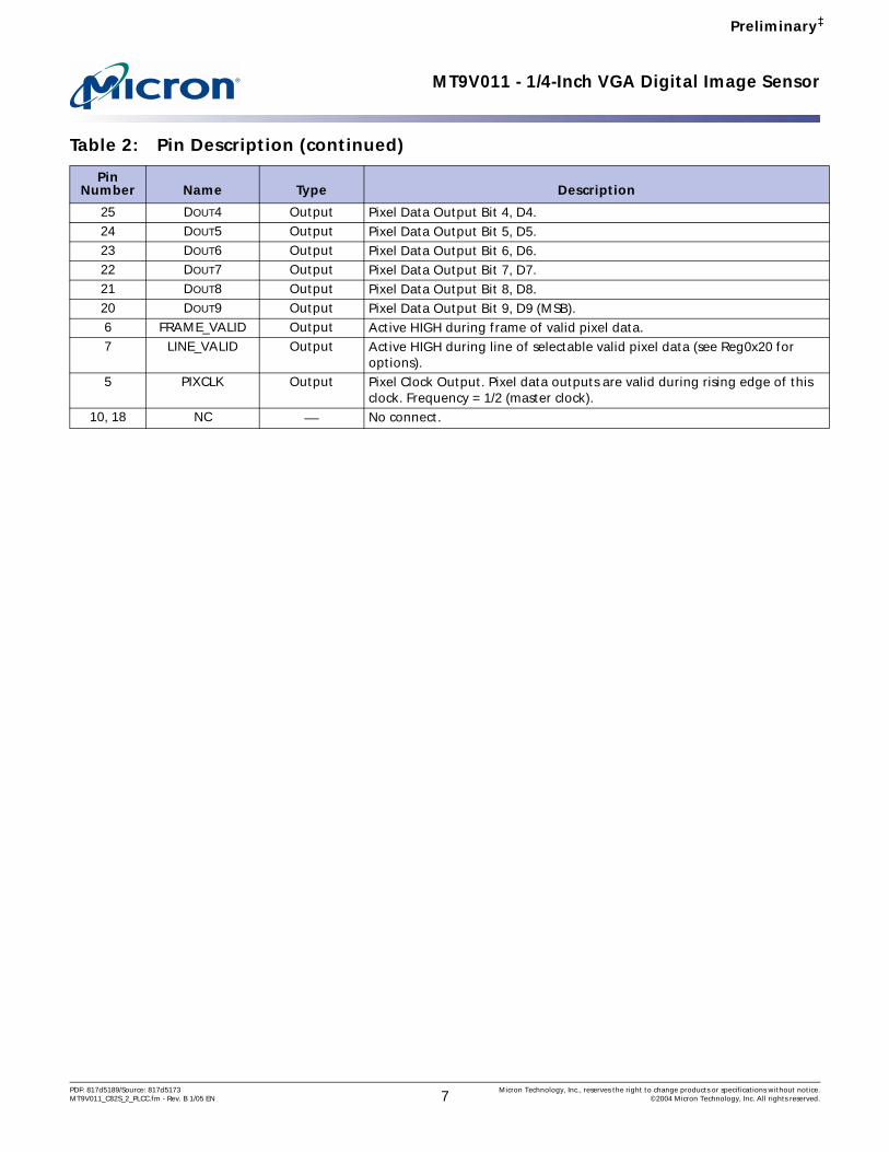
25 DOUT4 Output Pixel Data Output Bit 4, D4.24 DOUT5 Output Pixel Data Output Bit 5, D5.23 DOUT6 Output Pixel Data Output Bit 6, D6.22 DOUT7 Output Pixel Data Output Bit 7, D7.21 DOUT8 Output Pixel Data Output Bit 8, D8.20 DOUT9 Output Pixel Data Output Bit 9, D9 (MSB).6 FRAME_VALID Output Active HIGH during frame of valid pixel data.7 LINE_VALID Output Active HIGH during line of selectable valid pixel data (see Reg0x20 for
options).5 PIXCLK Output Pixel Clock Output. Pixel data outputs are valid during rising edge of this
clock. Frequency = 1/2 (master clock).10, 18 NC — No connect.
Table 2: Pin Description (continued)
Pin Number Name Type Description
PDF: 817d5189/Source: 817d5173 Micron Technology, Inc., reserves the right to change products or specifications without notice.MT9V011_C82S_2_PLCC.fm - Rev. B 1/05 EN 7 ©2004 Micron Technology, Inc. All rights reserved.

MT9V011 - 1/4-Inch VGA Digital Image SensorPixel Data Format
Preliminary‡
Pixel Data FormatPixel Array Structure
The MT9V011’s pixel array is 668 columns by 496 rows. The first 18 columns and the first 6 rows of pixels are optically black and can be used to monitor the black level. The last column and the last row of pixels are also optically black. The black row data is used internally for automatic black level adjustment. There are 649 columns by 489 rows of optically active pixels, which provides a four-pixel boundary around the VGA (640 x 480) image to avoid boundary affects during color interpolation and correction. The addi-tional active column and additional active row are used to allow horizontally and verti-cally mirrored readout to also start on the same color pixel, as shown in Figure 4.
Figure 4: Pixel Array Description
The MT9V011 uses the RGB Bayer color pattern. Even numbered rows contain green and red color pixels, and odd numbered rows contain blue and green color pixels. Likewise, even numbered columns contain green and blue color pixels, and odd numbered col-umns contain red and green color pixels.
Figure 5: Pixel Color Pattern Detail (Top Right Corner)
Output Data FormatThe MT9V011 image data is read-out in a progressive scan. Valid image data is sur-rounded by horizontal and vertical blanking, as shown in Figure 6. The amount of hori-zontal and vertical blanking is programmable through Reg0x05 and Reg0x06, respectively. LINE_VALID is HIGH during the shaded region of the figure. See “Output Data Timing” on page 9 for the description of FRAME_VALID timing.
(667,495)
18 black columns
1 black row
6 black rows (0, 0)
1 black column
VGA (640 x 480)+ 4 pixel boundary for
color correction+ additional active column
+ additional active row= 649 x 489 active pixels
B
G
B
G
B
G
B
R
B
G
G
R G R G
G G B
B
R
B
G
G
R G R G
G G B
B
R
B
G
G
R G R G
G G B
black pixels
…
…
…
column readout direction
row readout direction
Pixel (18, 6)(First Opticalclear pixel)
PDF: 817d5189/Source: 817d5173 Micron Technology, Inc., reserves the right to change products or specifications without notice.MT9V011_C82S_2_PLCC.fm - Rev. B 1/05 EN 8 ©2004 Micron Technology, Inc. All rights reserved.

MT9V011 - 1/4-Inch VGA Digital Image SensorPixel Data Format
Preliminary‡
Figure 6: Spatial Illustration of Image Readout
Output Data TimingThe data output of the MT9V011 is synchronized with the PIXCLK output. When LINE_VALID is HIGH, one 10-bit pixel datum is output every PIXCLK period.
Figure 7: Timing Example of Pixel Data
The rising edges of the PIXCLK signal are nominally timed to occur one-half of a master clock period after the DOUT edges. This allows PIXCLK to be used as a clock to latch the data. The PIXCLK is HIGH for one complete master clock period and then LOW for one complete master clock period. It is continuously enabled, even during the blanking period. The MT9V011 can be programmed to move the PIXCLK edge relative to the DOUT transitions from +1 to -1 master clock, in steps of one-half of a master clock. This can be achieved by programming the corresponding bits in Reg0x07.
The parameters P, A, and Q in Figure 8 are defined in Table 3.
Figure 8: Row Timing and FRAME_VALID/LINE_VALID Signals
P0,0 P0,1 P0,2.....................................P0,n-1 P0,nP1,0 P1,1 P1,2.....................................P1,n-1 P1,n
00 00 00 .................. 00 00 0000 00 00 .................. 00 00 00
Pm-1,0 Pm-1,1.....................................Pm-1,n-1 Pm-1,nPm,0 Pm,1.....................................Pm,n-1 Pm,n
00 00 00 .................. 00 00 0000 00 00 .................. 00 00 00
00 00 00 .................. 00 00 0000 00 00 .................. 00 00 00
00 00 00 .................. 00 00 0000 00 00 .................. 00 00 00
00 00 00 ..................................... 00 00 0000 00 00 ..................................... 00 00 00
00 00 00 ..................................... 00 00 0000 00 00 ..................................... 00 00 00
VALID IMAGE HORIZONTALBLANKING
VERTICAL BLANKING VERTICAL/HORIZONTALBLANKING
LINE_VALID
PIXCLK
DOUT9-DOUT0
. . . .
. . . .
. . . .
. . . .
P0(9:0)
P1(9:0)
P2(9:0)
P3(9:0)
P4(9:0)
Pn-1(9:0)
Pn(9:0)
Valid Image DataBlanking Blanking
P A Q A Q A P
. . .
. . .
. . .
Number of master clocks
FRAME_VALID
LINE_VALID
PDF: 817d5189/Source: 817d5173 Micron Technology, Inc., reserves the right to change products or specifications without notice.MT9V011_C82S_2_PLCC.fm - Rev. B 1/05 EN 9 ©2004 Micron Technology, Inc. All rights reserved.

MT9V011 - 1/4-Inch VGA Digital Image SensorPixel Data Format
Preliminary‡
Frame Timing Formulas
The constant 113 in the formulas in Table 3 is the constant value in default mode, when 8 dark columns are read out through Reg0x30. The constant follows the dark columns read out as shown in Table 4.
Sensor timing is shown above in terms of pixel clock and master clock cycles (please refer to Figure 7). The recommended master clock frequency is 27 MHz.
Table 4: Constant Value
The vertical blanking and total frame time equations assume that the number of integra-tion rows (bits 11 through 0 of Reg0x09) is less than the number of active plus blanking rows (Reg0x03 + 1 + Reg0x06 + 1). If this is not the case, the number of integration rows must be used instead to determine the frame time, as shown in Table 5.
Table 3: Frame Time
Parameter Name Equation Default Timing At 27 MHz
A Active Data Time (Reg0x04 + 1) x (Reg0x0A + 2) 640 pixel clocks= 1280 master= 47.4µs
P Frame Start/End Blanking 6 x (Reg0x0A + 2) 6 pixel clocks= 12 master= 0.44µs
Q Horizontal Blanking (113 + Reg0x05) x (Reg0x0A + 2)(minimum Reg0x05 value = 9)
244 pixel clocks= 488 master= 18.07µs
A+Q Row Time (Reg0x04 + 1 + 113 + Reg0x05) x (Reg0x0A + 2) 884 pixel clocks = 1,768 master= 65.48µs
V Vertical Blanking (Reg0x06 + 1) x (A + Q) + (Q - 2 x P) 25,868 pixel clocks= 51,736 master= 1.92ms
Nrows x (A + Q) Frame Valid Time (Reg0x03 + 1) x (A + Q) - (Q - 2 x P) 424,088 pixel clocks= 848,176 master= 31.41ms
F Total Frame Time (Reg0x03 + 1 + Reg0x06 + 1) x (A + Q) 449,956 pixel clocks= 899,912 master = 33.33ms
Reg 0x30, bit 1:0 Constant
1x 121 For 16 columns01 113 For 8 columns00 107 For no dark columns read, no row-wise noise correction applied
Table 5: Frame Time—Master Clock
Parameter Name Equation (Master Clock) Default Timing
V’ Vertical Blanking (long integration time)
(Reg0x09 - Reg0x03) x (A + Q) + (Q - 2 x P) 25,868 pixel clocks = 51,736 master = 1.92 ms
F’ Total Frame Time (long integration time)
(Reg0x09 + 1) x (A + Q) 449,956 pixel clocks = 899,912 master = 33.33ms
PDF: 817d5189/Source: 817d5173 Micron Technology, Inc., reserves the right to change products or specifications without notice.MT9V011_C82S_2_PLCC.fm - Rev. B 1/05 EN 10 ©2004 Micron Technology, Inc. All rights reserved.

MT9V011 - 1/4-Inch VGA Digital Image SensorSerial Bus Description
Preliminary‡
Serial Bus DescriptionRegisters are written to and read from the MT9V011 through the two-wire serial inter-face bus. The sensor is a serial interface slave and is controlled by the serial clock (SCLK), which is driven by the serial interface master. Data is transferred into and out through the MT9V011 serial data (SDATA) line. The SDATA line is pulled up to VDD off-chip by a 1.5KΩ resistor. Either the slave or master device can pull the SDATA line down—the serial interface protocol determines which device is allowed to pull the SDATA line down at any given time. The registers are 16 bits wide, and can be accessed through 16- or 8-bit two-wire serial bus sequences.
ProtocolThe two-wire serial interface defines several different transmission codes, as follows:
• a start bit• the slave device 8-bit address• a(n) (no) acknowledge bit• an 8-bit message• a stop bit
SequenceA typical read or write sequence begins by the master sending a start bit. After the start bit, the master sends the slave device’s 8-bit address. The last bit of the address deter-mines if the request will be a read or a write, where a “0” indicates a write and a “1” indi-cates a read. The slave device acknowledges its address by sending an acknowledge bit back to the master.
If the request was a write, the master then transfers the 8-bit register address to which a write should take place. The slave sends an acknowledge bit to indicate that the register address has been received. The master then transfers the data eight bits at a time, with the slave sending an acknowledge bit after each eight bits. The MT9V011 uses 16-bit data for its internal registers, thus requiring two 8-bit transfers to write to one register. After 16 bits are transferred, the register address is automatically incremented, so that the next 16 bits are written to the next register address. The master stops writing by sending a start or stop bit.
A typical read sequence is executed as follows. First the master sends the write-mode slave address and 8-bit register address, just as in the write request. The master then sends a start bit and the read-mode slave address. The master then clocks out the regis-ter data eight bits at a time. The master sends an acknowledge bit after each 8-bit trans-fer. The register address is auto-incremented after every 16 bits is transferred. The data transfer is stopped when the master sends a no-acknowledge bit. The MT9V011 allows for 8-bit data transfers through the two-wire serial interface by writing (or reading) the most significant eight bits to the register and then writing (or reading) the least signifi-cant eight bits to Reg0x80 (128).
Bus Idle StateThe bus is idle when both the data and clock lines are HIGH. Control of the bus is initi-ated with a start bit, and the bus is released with a stop bit. Only the master can generate the start and stop bits.
Start BitThe start bit is defined as a HIGH-to-LOW transition of the data line while the clock line is HIGH.
PDF: 817d5189/Source: 817d5173 Micron Technology, Inc., reserves the right to change products or specifications without notice.MT9V011_C82S_2_PLCC.fm - Rev. B 1/05 EN 11 ©2004 Micron Technology, Inc. All rights reserved.

MT9V011 - 1/4-Inch VGA Digital Image SensorSerial Bus Description
Preliminary‡
Stop BitThe stop bit is defined as a LOW-to-HIGH transition of the data line while the clock line is HIGH.
Slave AddressThe 8-bit address of a two-wire serial interface device consists of seven bits of address and 1 bit of direction. A “0” in the LSB of the address indicates write mode, and a “1” indicates read mode. The write address of the sensor is 0xBA, while the read address is 0xBB.
Data Bit TransferOne data bit is transferred during each clock pulse. The two-wire serial interface clock pulse is provided by the master. The data must be stable during the HIGH period of the serial clock—it can only change when the two-wire serial interface clock is LOW. Data is transferred eight bits at a time, followed by an acknowledge bit.
Acknowledge BitThe master generates the acknowledge clock pulse. The transmitter (which is the master when writing, or the slave when reading) releases the data line, and the receiver indi-cates an acknowledge bit by pulling the data line low during the acknowledge clock pulse.
No-Acknowledge BitThe no-acknowledge bit is generated when the data line is not pulled down by the receiver during the acknowledge clock pulse. A no-acknowledge bit is used to terminate a read sequence.
PDF: 817d5189/Source: 817d5173 Micron Technology, Inc., reserves the right to change products or specifications without notice.MT9V011_C82S_2_PLCC.fm - Rev. B 1/05 EN 12 ©2004 Micron Technology, Inc. All rights reserved.
MT9V011 - 1/4-Inch VGA Digital Image SensorTwo-wire Serial Interface Sample Read and Write Sequences
Preliminary‡
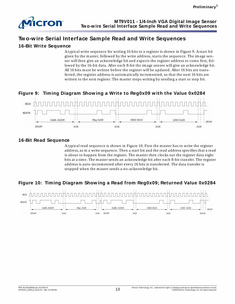
Two-wire Serial Interface Sample Read and Write Sequences16-Bit Write Sequence
A typical write sequence for writing 16 bits to a register is shown in Figure 9. A start bit given by the master, followed by the write address, starts the sequence. The image sen-sor will then give an acknowledge bit and expects the register address to come first, fol-lowed by the 16-bit data. After each 8-bit the image sensor will give an acknowledge bit. All 16 bits must be written before the register will be updated. After 16 bits are trans-ferred, the register address is automatically incremented, so that the next 16 bits are written to the next register. The master stops writing by sending a start or stop bit.
Figure 9: Timing Diagram Showing a Write to Reg0x09 with the Value 0x0284
16-Bit Read SequenceA typical read sequence is shown in Figure 10. First the master has to write the register address, as in a write sequence. Then a start bit and the read address specifies that a read is about to happen from the register. The master then clocks out the register data eight bits at a time. The master sends an acknowledge bit after each 8-bit transfer. The register address is auto-incremented after every 16 bits is transferred. The data transfer is stopped when the master sends a no-acknowledge bit.
Figure 10: Timing Diagram Showing a Read from Reg0x09; Returned Value 0x0284
SCLK
SDATA
START ACK
0xBA ADDR
ACK ACK ACK
STOPReg 0x09 1000 01000000 0010
SCLK
SDATA
START ACK
0xBA ADDR 0xBB ADDR 0000 0010Reg 0x09
ACK ACK ACK
STOP1000 0100
NACKSTART
PDF: 817d5189/Source: 817d5173 Micron Technology, Inc., reserves the right to change products or specifications without notice.MT9V011_C82S_2_PLCC.fm - Rev. B 1/05 EN 13 ©2004 Micron Technology, Inc. All rights reserved.
MT9V011 - 1/4-Inch VGA Digital Image SensorTwo-wire Serial Interface Sample Read and Write Sequences
Preliminary‡
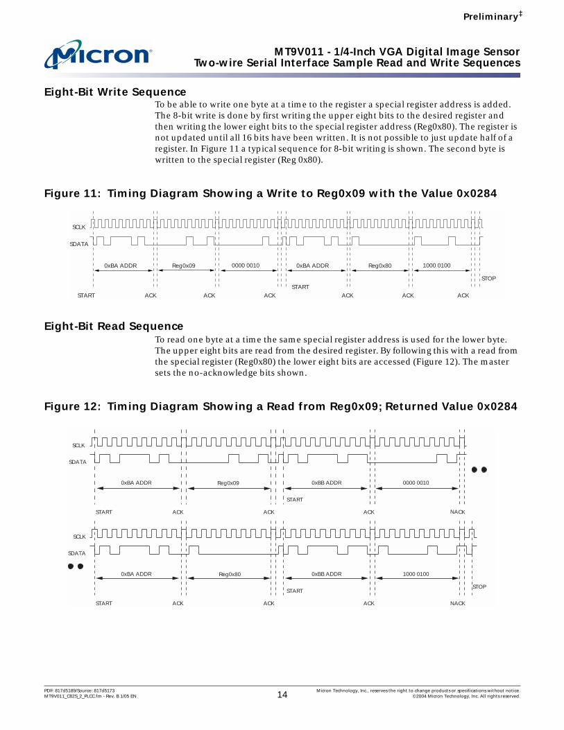
Eight-Bit Write SequenceTo be able to write one byte at a time to the register a special register address is added. The 8-bit write is done by first writing the upper eight bits to the desired register and then writing the lower eight bits to the special register address (Reg0x80). The register is not updated until all 16 bits have been written. It is not possible to just update half of a register. In Figure 11 a typical sequence for 8-bit writing is shown. The second byte is written to the special register (Reg 0x80).
Figure 11: Timing Diagram Showing a Write to Reg0x09 with the Value 0x0284
Eight-Bit Read SequenceTo read one byte at a time the same special register address is used for the lower byte. The upper eight bits are read from the desired register. By following this with a read from the special register (Reg0x80) the lower eight bits are accessed (Figure 12). The master sets the no-acknowledge bits shown.
Figure 12: Timing Diagram Showing a Read from Reg0x09; Returned Value 0x0284
STOP
Reg0x80
ACKSTART
0xBA ADDR
ACK
SDATA
SCLK
ACKACKACKACK
Reg0x090xBA ADDR 0000 0010 1000 0100
START
START
0xBB ADDR
SDATA
SCLK
STOP
NACKACKACKACK
Reg0x09
START
0xBA ADDR 0000 0010
START
0xBB ADDR
SDATA
SCLK
NACKACKACKACK
Reg0x80
START
0xBA ADDR 1000 0100
PDF: 817d5189/Source: 817d5173 Micron Technology, Inc., reserves the right to change products or specifications without notice.MT9V011_C82S_2_PLCC.fm - Rev. B 1/05 EN 14 ©2004 Micron Technology, Inc. All rights reserved.

MT9V011 - 1/4-Inch VGA Digital Image SensorRegisters
Preliminary‡
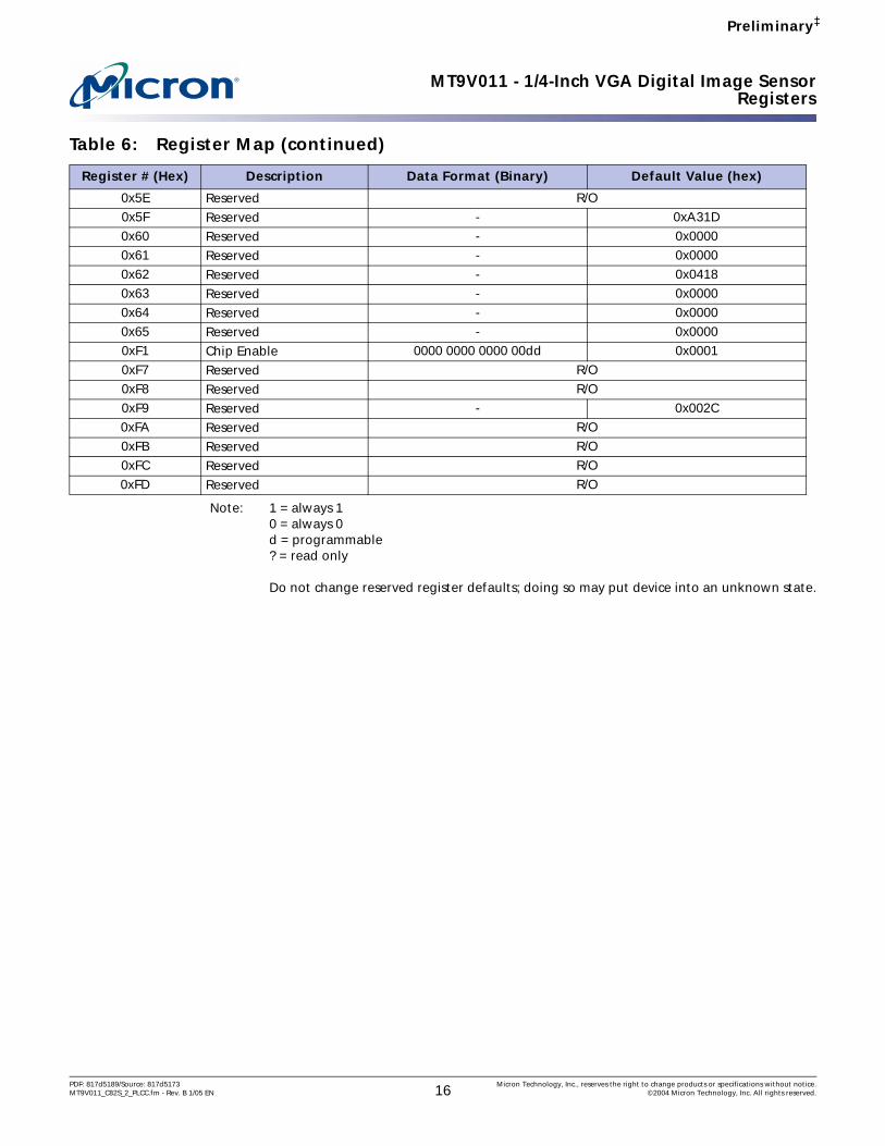
RegistersRegister Map Table 6: Register Map
Register # (Hex) Description Data Format (Binary) Default Value (hex)
0x00/0xFF Chip Version 1000 0010 0011 0010 0x82430x01 Row Start 0000 000d dddd dddd 0x000A0x02 Column Start 0000 00dd dddd dddd 0x00160x03 Window Height 0000 000d dddd dddd 0x01DF0x04 Window Width 0000 00dd dddd dddd 0x027F0x05 Horizontal Blanking 0000 00dd dddd dddd 0x00830x06 Vertical Blanking 0000 dddd dddd dddd 0x001C0x07 Output Control dddd dddd dddd dddd 0x30020x09 Shutter Width 0000 dddd dddd dddd 0x01FC0x0A Pixel Clock Speed 0000 0000 000d dddd 0x00000x0B Restart 0000 0000 0000 000d 0x00000x0C Shutter Delay 0000 00dd dddd dddd 0x00000x0D Reset 0000 0000 0000 000d 0x00000x1E Digital Zoom 0000 0ddd 0000 00dd 0x00000x20 Read Mode dddd dddd dddd dddd 0x10000x21 Reserved - 0x00000x22 Reserved - 0x00000x27 Reserved - 0x00240x2B Green1 Gain 0000 0ddd dddd dddd 0x00200x2C Blue Gain 0000 0ddd dddd dddd 0x00200x2D Red Gain 0000 0ddd dddd dddd 0x00200x2E Green2 Gain 0000 0ddd dddd dddd 0x00200x2F Reserved - 0xF7B00x30 Reserved - 0x00050x31 Reserved - 0x002A0x32 Reserved - 0x00000x33 Reserved - 0x300F0x34 Reserved - 0x01000x35 Global Gain 0000 0ddd dddd dddd 0x00200x3B Reserved N/A0x3C Reserved - 0x08200x3D Reserved - 0x068F0x3E Reserved N/A0x3F Reserved - 0x06A00x40 Reserved - 0x01E00x41 Reserved - 0x00D10x42 Reserved - 0x08820x58 Reserved - 0x00780x59 Reserved - 0x07030x5A Reserved - 0x04270x5B Reserved R/O0x5C Reserved R/O0x5D Reserved R/O
PDF: 817d5189/Source: 817d5173 Micron Technology, Inc., reserves the right to change products or specifications without notice.MT9V011_C82S_2_PLCC.fm - Rev. B 1/05 EN 15 ©2004 Micron Technology, Inc. All rights reserved.
MT9V011 - 1/4-Inch VGA Digital Image SensorRegisters
Preliminary‡
Note: 1 = always 10 = always 0d = programmable? = read only
Do not change reserved register defaults; doing so may put device into an unknown state.
0x5E Reserved R/O0x5F Reserved - 0xA31D0x60 Reserved - 0x00000x61 Reserved - 0x00000x62 Reserved - 0x04180x63 Reserved - 0x00000x64 Reserved - 0x00000x65 Reserved - 0x00000xF1 Chip Enable 0000 0000 0000 00dd 0x00010xF7 Reserved R/O0xF8 Reserved R/O0xF9 Reserved - 0x002C0xFA Reserved R/O0xFB Reserved R/O0xFC Reserved R/O0xFD Reserved R/O
Table 6: Register Map (continued)
Register # (Hex) Description Data Format (Binary) Default Value (hex)
PDF: 817d5189/Source: 817d5173 Micron Technology, Inc., reserves the right to change products or specifications without notice.MT9V011_C82S_2_PLCC.fm - Rev. B 1/05 EN 16 ©2004 Micron Technology, Inc. All rights reserved.

MT9V011 - 1/4-Inch VGA Digital Image SensorRegisters
Preliminary‡
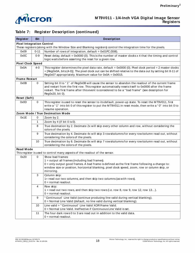
Register DescriptionsTable 7: Register Description
Register Bit Description
Chip Version0x00 / 0xFF 0-15 This register is read-only and gives the chip identification number: 0x8243.Window ControlThese registers control the size of the window.
0x01 0-8 First row to be read out—default = 0x000A (10).Minimum recommended value = 0x0006.
0x02 0-9 First column to be read out—default = 0x0016 (22). Minimum recommended value = 0x0012 (18).0x03 0-8 Window height (number of rows - 1)—default = 0x01DF (479).0x04 0-9 Window width (number of columns - 1)—default = 0x027F (639).
Minimum recommended value = 0x0009.Blanking ControlThese registers control the blanking time in a row and between frames.
0x05 0-9 Horizontal Blanking (number of columns)—default = 0x0083 (131 pixel clocks).Minimum value for 0x05 = 0x0009.Minimum recommended value for 0x05 = 0x007B (123 pixel clocks).
0x06 0-11 Vertical Blanking (number of rows -1)—default = 0x001C (28 rows). Minimum recommended value = 0x0003.
Output ControlThis register controls various features of the output format for the sensor.
0x07 0 Synchronize changes (copied to Reg0xF1, bit1).0 = normal operation, update changes to registers that affect image brightness (integration time, integration delay, gain, horizontal and vertical blanking, window size, row/column skip, or row mirror) at the next frame boundary.1 = do not update any changes to these settings until this bit is returned to “0.”
1 Chip Enable (copied to Reg0xF1, bit0).1 = normal operation.0 = stop sensor readout. When this is returned to “1,” sensor readout restarts at the starting row in a new frame. The digital power consumption can then also be reduced to less than 5uA by turning off the master clock.
4 By setting this bit to “1,” the sampling and reset timing of the pixels will be halved. This bit should therefore only be used if the master clock frequency is 13.5 MHz or less. When this bit is set the minimum recommended horizontal blanking value is 17, compared to 123 when this bit is not set. Shutter Delay will be master clocks divided by 2 when this bit is set, compared to master clocks divided by 4 when this bit is 0.Note: Use this register for 15 fps with 12 MHz master clock.
5 Allow Shutter Width to be exactly one full frame.0 = normal operation = Maximum Shutter Width equals the total number of rows - 1. If Shutter Width exceeds the number of rows -1, the total number of rows in the image will be increased to Shutter Width + 1.1 = Maximum Shutter Width equals the total number of rows. When the Shutter Width exceeds the number of rows, the total number of rows in the image will be increased to match the Shutter Width.
6 Reserved.0 = normal operation.
8 -11 Shift pixel clock: (11,10,9,8) = (1, x, x, x): shift pixel clock 1 clock earlier (0, 1, x, x): shift pixel clock ½ clock earlier (0, 0, 1, x): delay pixel clock by ½ clock(0, 0, 0, 1): delay pixel clock by 1 clock (0, 0, 0, 0): no delay pixel clock (default mode).
15 Invert pixel clock:0 = normal operation.1 = invert pixel clock.
PDF: 817d5189/Source: 817d5173 Micron Technology, Inc., reserves the right to change products or specifications without notice.MT9V011_C82S_2_PLCC.fm - Rev. B 1/05 EN 17 ©2004 Micron Technology, Inc. All rights reserved.
MT9V011 - 1/4-Inch VGA Digital Image SensorRegisters
Preliminary‡
Pixel Integration ControlThese registers (along with the Window Size and Blanking registers) control the integration time for the pixels.
0x09 0-11 Number of rows of integration, default = 0x01FC (508). 0x0C 0-9 Reset delay, default = 0x0000 (0). This is the number of master clocks x 4 that the timing and control
logic waits before asserting the reset for a given row.Pixel Clock Speed
0x0A 4-0 This register determines the pixel data rate, default = 0x0000 (0). Pixel clock period = 2 master clocks + [Reg0x0A, bits (4-0)]. The pixel clock out can be shifted relative to the data out by setting bit 8-11 of Reg0x07 appropriately. Maximum value for 0x0A = 0x0015.
Frame Restart0x0B 0 Setting bit 0 to “1” of Reg0x0B will cause the sensor to abandon the readout of the current frame
and restart from the first row. This register automatically resets itself to 0x0000 after the frame restart. The first frame after this event is considered to be a "bad frame" (see description for Reg0x20, bit 0).
Reset (Soft)0x0D 0 This register is used to reset the sensor to its default, power-up state. To reset the MT9V011, first
write a “1” into bit 0 of this register to put the MT9V011 in reset mode, then write a “0” into bit 0 to resume operation.
Zoom Mode / True Decimation Mode0x1E 0 Zoom by 2.
1 Zoom by 4 (if bit 0 is 0).8 True decimation by 2. Decimate 2x will skip every other column and row, without considering the
colors of the pixels. 9 True decimation by 4. Decimate 4x will skip 3 rows/columns for every row/column read out, without
considering the colors of the pixels. 10 True decimation by 8. Decimate 8x will skip 7 rows/columns for every row/column read out, without
considering the colors of the pixels. Read ModeThis register is used to control many aspects of the readout of the sensor.
0x20 0 Show bad frames: 1 = output all frames (including bad frames).0 = only output good frames. A bad frame is defined as the first frame following a change to: window size or position, horizontal blanking, pixel clock speed, zoom, row or column skip, or mirroring.
3 Column skip: 1= read out two columns, and then skip two columns (as with rows).0 = normal readout.
4 Row skip:1 = read out two rows, and then skip two rows (i.e. row 8, row 9, row 12, row 13…).0 = normal readout.
9 "Continuous" Line Valid (continue producing line valid during vertical blanking).0 = Normal Line Valid (default, no line valid during vertical blanking).
10 Line valid = "Continuous" Line Valid XOR Frame Valid.0 = Normal Line Valid. Ineffective if Continuous Line Valid is set.
11 The four dark rows 0 to 3 are read out in addition to the valid data.0 = normal readout.
Table 7: Register Description (continued)
Register Bit Description
PDF: 817d5189/Source: 817d5173 Micron Technology, Inc., reserves the right to change products or specifications without notice.MT9V011_C82S_2_PLCC.fm - Rev. B 1/05 EN 18 ©2004 Micron Technology, Inc. All rights reserved.

MT9V011 - 1/4-Inch VGA Digital Image SensorRegisters
Preliminary‡
To preserve a right-reading image and the correct color order, all four of these bits should be set to “1” to invert the image.
5 1 = readout starting 1 column later.0 = normal readout.
7 1 = readout starting 1 row later.0 = normal readout.
14 1 = read out from right to left (mirrored).0 = normal readout.
15 1 = read out from bottom to top (upside down).0 = normal readout.
Gain SettingsThe gain can be individually controlled for each color in the Bayer pattern.
0x2B Green1 Gain—default = 0x0020 (32) = 1x gain.0-6 Initial Gain = bits (6:0) x 0.03125.7, 8 Analog Gain = (Bit 8 + 1) x (Bit 7 + 1) x Initial Gain (each bit gives 2x gain).9,10 9, 10: Total Gain = (Bit 9 + 1) x (Bit 10 + 1) x Analog Gain (each bit gives 2x gain).
0x2C Blue Gain—default = 0x0020 (32) = 1x gain.0-6 Initial Gain = bits (6-0) x 0.03125.7, 8 Analog gain = (Bit 8 + 1) x (Bit 7 + 1) x Initial Gain (each bit gives 2x gain).9,10 9, 10: Total Gain = (Bit 9 + 1) x (Bit 10 + 1) x Analog Gain (each bit gives 2x gain).
0x2D Red gain—default = 0x0020 (32) = 1x gain.0-6 Initial Gain = bits (6-0) x 0.03125.7, 8 Analog Gain = (Bit 8 + 1) x (Bit 7 + 1) x Initial Gain (each bit gives 2x gain).9,10 9, 10: Total Gain = (Bit 9 + 1) x (Bit 10 + 1) x Analog Gain (each bit gives 2x gain).
0x2E Green2 gain—default = 0x0020 (32) = 1x gain.0-6 Initial Gain = bits (6-0) x 0.03125.7, 8 Analog Gain = (Bit 8 + 1) x (Bit 7 + 1) x Initial Gain (each bit gives 2x gain).9,10 9, 10: Total gain = (Bit 9 + 1) x (Bit 10 + 1) x Analog Gain (each bit gives 2x gain).
0x35 GlobalGain—default = 0x0020 (32) = 1x gain. This register can be used to set all four gains at once. When read, it will return the value stored in Reg0x2B.
0-6 Initial Gain = bits (6-0) x 0.03125.7, 8 Analog Gain = (Bit 8 + 1) x (Bit 7 + 1) x Initial Gain (each bit gives 2x gain).9,10 9, 10: Total Gain = (Bit 9 + 1) x (Bit 10 + 1) x Analog Gain (each bit gives 2x gain).
Table 7: Register Description (continued)
Register Bit Description
PDF: 817d5189/Source: 817d5173 Micron Technology, Inc., reserves the right to change products or specifications without notice.MT9V011_C82S_2_PLCC.fm - Rev. B 1/05 EN 19 ©2004 Micron Technology, Inc. All rights reserved.

MT9V011 - 1/4-Inch VGA Digital Image SensorFeature Description
Preliminary‡
Feature DescriptionWindow Control
Reg0x01 Row Start, Reg0x02 Column Start, Reg0x03 Window Height (row size), and Reg0x04 Window Width (column size)
These registers control the size and starting coordinates of the window. By changing these registers, any image format smaller than or equal to VGA can be specified.
Blanking Control Reg0x05 Horizontal Blanking, and Reg0x06 Vertical Blanking
Blanking Control:
These registers control the blanking time in a row (called column fill-in or horizontal blanking) and between frames (vertical blanking).
• Horizontal blanking is specified in terms of pixel clocks.• Vertical blanking is specified in terms of row readout times. (The programmed value
is one less than the actual value.)The actual imager timing can be calculated using Table 3 on page 10 which describes "Row Timing and FRAME_VALID/LINE_VALID Signals.”
The number of dark rows read out depends on the vertical blanking set as shown in the Table 8.
Pixel Integration Control Reg0x09 Shutter Width, and Reg0x0C Shutter Delay
These registers (along with the Window Size and horizontal blanking registers) control the integration time for the pixels.
Reg0x09: number of rows of integration, default = 0x01FC (508)
Reg0x0C: reset delay, default = 0x0000 (0). This is the number of master clocks that the timing and control logic waits before asserting the reset for a given row.
The actual total integration time, tINT, is:
tINT =
Reg0x09 x Row Time - Overhead time - Reset delay, where:
Row Time = (Reg0x04 + 1 + 113 + Reg0x05) x (Reg0x0A + 2) master clock periods
Overhead time = K x 57 master clock periods
Reset delay = K x Reg0x0C master clock periods
If the value in Reg0x0C exceeds (row time - 444)/K master clock cycles, the row time will be extended by (K x Reg0x0C - (row time - 444)) clock cycles.
Where :
K = 4 when Reg0x07[4] = 0, and
Table 8: Vertical Blanking
Reg0x06 # Dark Rows
0 01-2 23+ 4
PDF: 817d5189/Source: 817d5173 Micron Technology, Inc., reserves the right to change products or specifications without notice.MT9V011_C82S_2_PLCC.fm - Rev. B 1/05 EN 20 ©2004 Micron Technology, Inc. All rights reserved.

MT9V011 - 1/4-Inch VGA Digital Image SensorFeature Description
Preliminary‡
K = 2 when Reg0x07[4] = 1
In this expression the row time term corresponds to the number of rows integrated. The overhead time is the time between the READ cycle and the RESET cycle, and the final term is the effect of the reset delay.
Typically, the value of Reg0x09 (Shutter Width) is limited to the number of rows per frame (which includes vertical blanking rows), such that the frame rate is not affected by the integration time. If Reg0x09 is increased beyond the total number of rows per frame, the MT9V011 will add additional blanking rows as needed. A second constraint is that tINT must be adjusted to avoid banding in the image from light flicker. Under 60 Hz flicker, this means tINT must be a multiple of 1/120 of a second. Under 50 Hz flicker, tINT must be a multiple of 1/100 of a second.
Pixel Clock Speed Reg0x0A Pixel Clock Speed
The pixel clock speed is set by Reg0x0A. The pixel clock period will be the number set plus two master clock cycles. The default value is 0, which is equal to 2 master clock cycles. With a master clock frequency of 27 MHz the PIXCLK frequency will be 13.5 MHz. The pixel clock out can be shifted relative to the data out by setting bit 8-11 of Reg0x07 appropriately.
Reset Reg0x0D Reset
This register is used to reset the sensor to its default, power-up state. To reset the MT9V011, first write a “1” into bit 0 of this register, then write a “0” into bit 0 to resume operation.
Digital Zoom Reg0x1E Digital Zoom/True decimation
In zoom mode, the pixel data rate is slowed down by a factor of either 2 or 4, and either 1 or 3 additional blank rows are added between each output row. This is designed to give the controller logic time to repeat data to fill in a window that is either 2 or 4 times larger with repeated data.
The pixel clock speed is not affected by this operation, and the output data for each pixel is valid for either 2 or 4 pixel clocks. In zoom by 2 mode, every row is followed by a blank row (with its own line valid, but all data bits = 0) of equal time. In zoom by 4 mode, every row is followed by three blank rows. The combination of this register and an appropriate change to the window sizing registers allows the user to zoom to a region of interest without affecting the frame rate.
PDF: 817d5189/Source: 817d5173 Micron Technology, Inc., reserves the right to change products or specifications without notice.MT9V011_C82S_2_PLCC.fm - Rev. B 1/05 EN 21 ©2004 Micron Technology, Inc. All rights reserved.

MT9V011 - 1/4-Inch VGA Digital Image SensorFeature Description
Preliminary‡
Figure 13: Readout of 4 Pixels in Normal and Zoom 2x Output Mode
True Decimation modeReg0x1E Digital Zoom/True decimation
True decimation mode is intended for use in sensors without color filtering. There are three modes with different amount of decimation. In decimate 2x every other column and row are skipped. In decimate 4x three rows/columns will be skipped for every row/column read out, and in decimate 8x seven rows/columns will be skipped for every row/column read out. Decimate 2x is shown in Figure 14. In decimation mode the global gain register should be used to set the gain.
Figure 14: Readout of 8 Pixels in Normal and 2x Decimation Output Mode
Read Mode
Column Mirror imageBy setting bits 14 and 5 of Reg0x20 the readout order of the columns will be reversed, as shown in Figure 15.
Figure 15: Readout of 6 Pixels in Normal and Column Mirror Output Mode
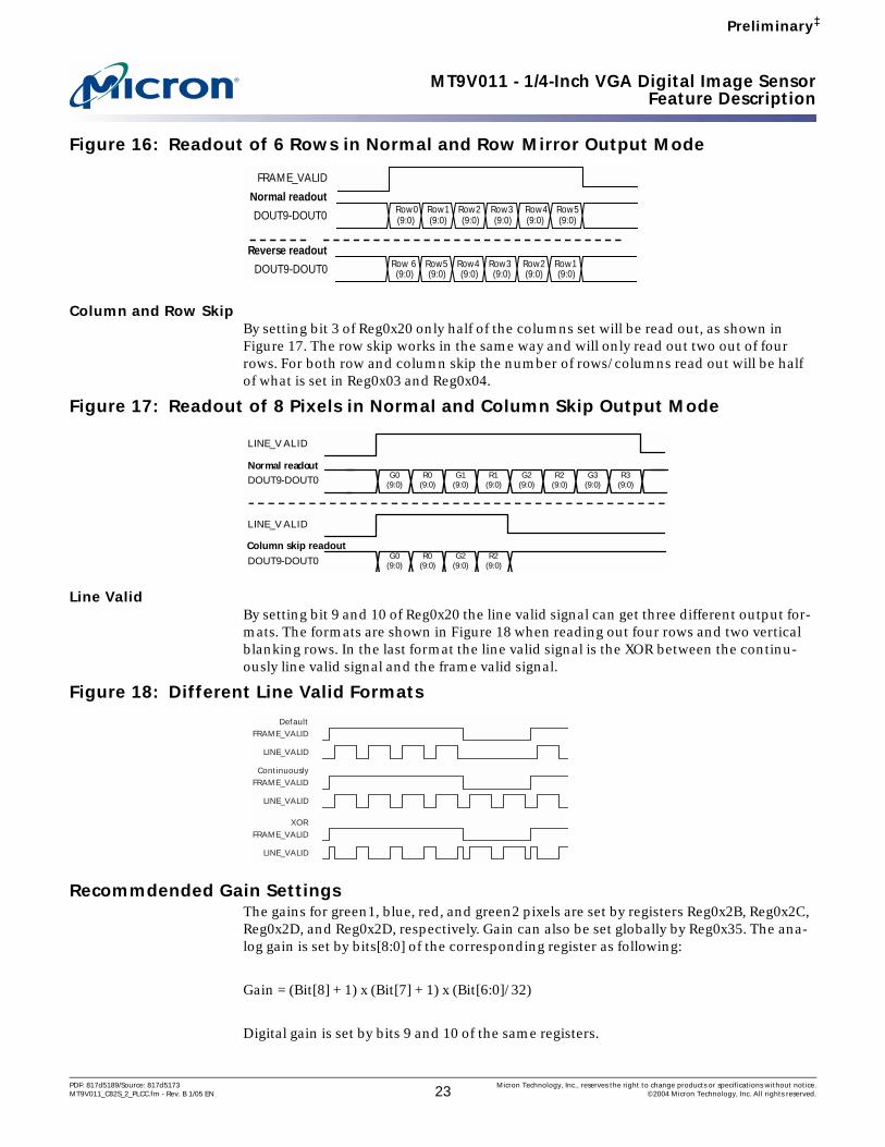
Row Mirror ImageBy setting bits 15 and 7 of Reg0x20 the readout order of the rows will be reversed, as shown in Figure 16.
LINE_VALID
DOUT9-DOUT0
PIXCLK
Normal readout
LINE_VALID
PIXCLK
Zoom 2X readout
G0(9:0)
R0(9:0)
G1(9:0)
R1(9:0)
R1(9:0)
G1(9:0)
R0(9:0)
G0(9:0) DOUT9-DOUT0
P0 (9:0)
P1 (9:0)
P2 (9:0)
P3 (9:0)
P4 (9:0)
P5 (9:0)
P6 (9:0)
P7 (9:0)
P0(9:0)
P2 (9:0)
P4 (9:0)
P6 (9:0)
LINE_VALID
DOUT9-DOUT0
Normal readout
LINE_VALID
DOUT9-DOUT0
Decimate 2X readout
LINE_VALID
DOUT9-DOUT0
Normal readout
DOUT9-DOUT0
Reverse readout
G0 (9:0)
R0 (9:0)
G1 (9:0)
R1 (9:0)
G2 (9:0)
R2 (9:0)
G3 (9:0)
R2(9:0)
G2 (9:0)
R1 (9:0)
G1 (9:0)
R0 (9:0)
PDF: 817d5189/Source: 817d5173 Micron Technology, Inc., reserves the right to change products or specifications without notice.MT9V011_C82S_2_PLCC.fm - Rev. B 1/05 EN 22 ©2004 Micron Technology, Inc. All rights reserved.
MT9V011 - 1/4-Inch VGA Digital Image SensorFeature Description
Preliminary‡
Figure 16: Readout of 6 Rows in Normal and Row Mirror Output Mode
Column and Row SkipBy setting bit 3 of Reg0x20 only half of the columns set will be read out, as shown in Figure 17. The row skip works in the same way and will only read out two out of four rows. For both row and column skip the number of rows/columns read out will be half of what is set in Reg0x03 and Reg0x04.
Figure 17: Readout of 8 Pixels in Normal and Column Skip Output Mode
Line ValidBy setting bit 9 and 10 of Reg0x20 the line valid signal can get three different output for-mats. The formats are shown in Figure 18 when reading out four rows and two vertical blanking rows. In the last format the line valid signal is the XOR between the continu-ously line valid signal and the frame valid signal.
Figure 18: Different Line Valid Formats
Recommdended Gain SettingsThe gains for green1, blue, red, and green2 pixels are set by registers Reg0x2B, Reg0x2C, Reg0x2D, and Reg0x2D, respectively. Gain can also be set globally by Reg0x35. The ana-log gain is set by bits[8:0] of the corresponding register as following:
Gain = (Bit[8] + 1) x (Bit[7] + 1) x (Bit[6:0]/32)
Digital gain is set by bits 9 and 10 of the same registers.
FRAME_VALID
DOUT9-DOUT0 Row0(9:0)
Row1(9:0)
Row2(9:0)
Row3(9:0)
Row4(9:0)
Row5(9:0)
Normal readout
DOUT9-DOUT0 (9:0) (9:0) (9:0) (9:0) (9:0) (9:0)
Reverse readoutRow 6 Row5 Row4 Row3 Row2 Row1
DOUT9-DOUT0 G0(9:0)
R0(9:0)
G1(9:0)
R1(9:0)
G2(9:0)
R2(9:0)
LINE_V ALID
Normal readout
DOUT9-DOUT0
Column skip readout
G3(9:0)
R3(9:0)
G0(9:0)
R0(9:0)
G2(9:0)
R2(9:0)
LINE_V ALID
DefaultFRAME_VALID
LINE_VALID
ContinuouslyFRAME_VALID
LINE_VALID
XORFRAME_VALID
LINE_VALID
PDF: 817d5189/Source: 817d5173 Micron Technology, Inc., reserves the right to change products or specifications without notice.MT9V011_C82S_2_PLCC.fm - Rev. B 1/05 EN 23 ©2004 Micron Technology, Inc. All rights reserved.

MT9V011 - 1/4-Inch VGA Digital Image SensorFeature Description
Preliminary‡
The analog gain circuitry (pre-ADC) is designed to offer signal gains from 1 to 15.875.
The minimum gain of 1 (register set to 0x0020) corresponds to the lowest setting where the pixel signal is guaranteed to saturate the ADC under all specified operating condi-tions. Any reduction of the gain below this value may cause the sensor to saturate at ADC output values less than the maximum, under certain conditions. It is recom-mended that this guideline be followed at all times.
Since bits 7 and 8 of the gain registers are multiplicative factors for the gain settings, there are alternative ways of achieving certain gains. Some settings offer superior noise performance to others, while the same overall gain. Table 9 lists the recommended gain settings.
Table 9: Recommended Gain Settings
Desired GainRecommended Settings
(Gain Registers) Conversion Formula (Arithmetic)
1.000 to 1.969 0x0020 to 0x003F (Register value)/322.000 to 7.938 0x00A0 to 0x00FF (Register value - 128)/16
8.000 to 15.875 0x01C0 to 0x01FF (Register value - 384)/8
PDF: 817d5189/Source: 817d5173 Micron Technology, Inc., reserves the right to change products or specifications without notice.MT9V011_C82S_2_PLCC.fm - Rev. B 1/05 EN 24 ©2004 Micron Technology, Inc. All rights reserved.

MT9V011 - 1/4-Inch VGA Digital Image SensorElectrical Specifications
Preliminary‡
Electrical Specifications
Note: 1. To place the chip in standby mode, first raise STANDBY to VDD, then wait two master clock cycles before turning off the master clock. Two master clock cycles are required to place the analog circuitry into standby, low-power mode.
2. When STANDBY is de-asserted, standby mode is exited immediately (within several master clocks), but the current frame and the next two frames will be invalid. The fourth frame will contain a valid image.
Table 10: DC Electrical Characteristics (VDD = VAA = 2.8 ±0.25V; TA = Ambient = 25°C; 30 fps at 27 MHz)
Symbol Definition Condition Min typ Max Unit Notes
VIH Input High Voltage VDD-0.25 VDD+0.25 V
VIL Input Low Voltage -0.3 0.8 V
IIN Input Leakage Current No Pull-up Resistor; VIN = VDD or DGND
-5 5 µA
VOH Output High Voltage VDD-0.2 V
VOL Output Low Voltage 0.2 V
IOH Output High Current 15.0 mA
IOL Output Low Current 20.0 mA
IOZ Tri-state Output Leakage Current
5.0 µA
IAA Analog Operating Current
CLKIN = 27 MHz; default setting, CLOAD = 10pF
14.0 20.0 28.0 mA
IDD Digital Operating Current
CLKIN = 27 MHz; default setting, CLOAD = 10pF
3.0 5.0 8.0 mA
IAA Standby Analog Standby Supply Current
STDBY = VDD 0.0 0.0 5.0 µA 1, 2
IDD Standby Digital Standby Supply Current
STDBY = VDD 0.0 1.0 5.0 µA 1, 2
PDF: 817d5189/Source: 817d5173 Micron Technology, Inc., reserves the right to change products or specifications without notice.MT9V011_C82S_2_PLCC.fm - Rev. B 1/05 EN 25 ©2004 Micron Technology, Inc. All rights reserved.

MT9V011 - 1/4-Inch VGA Digital Image SensorElectrical Specifications
Preliminary‡
Notes: 1. For 30 fps operation with a 27 MHz clock, it is very important to have a precise duty cycle equal to 50%. With a slower frame rate and a slower clock the clock duty cycle can be relaxed.
Table 11: AC Electrical Characteristics(VDD = VAA = 2.8 ±0.25V; TA = Ambient = 25°C; 30 fps at 27 MHz)
Symbol Definition Condition Min Typ Max Unit Notes
fCLKIN Input Clock Frequency 27 27 MHz
Clock Duty Cycle 45 50 55 % 1tR Input Clock Rise Time 2.5 nstF Input Clock Fall Time 2.0 ns
tPLHP tPHLP
CLKIN to PIXCLK propagation delay:LOW-to-HIGHHIGH-TO-LOW
CLOAD = 10pF12.010.0
ns
tDSETUP tDHOLD
PIXCLK to DOUT(9:0) Setup TimeHold Time
CLOAD = 10pF 15.014.0
ns
tOH Data Hold Time from PIXCLK falling edge 9.0 ns
tPLHF,L tPHLF,L
CLKIN to FRAME_VALID and LINE_VALID propagation delay:LOW-to-HIGH, HIGH-to-LOW
CLOAD = 10pF
12.011.0
ns
tPLHDtPHLD
CLKIN to DOUT (9:0) propagation delay:LOW-to-HIGH, HIGH-to-LOW
CLOAD = 10pF7.57.0
ns
tOUTR Output Rise Time CLOAD = 10pF 7.0 nstOUTF Output Fall Time CLOAD = 10pF 9.0 ns
PDF: 817d5189/Source: 817d5173 Micron Technology, Inc., reserves the right to change products or specifications without notice.MT9V011_C82S_2_PLCC.fm - Rev. B 1/05 EN 26 ©2004 Micron Technology, Inc. All rights reserved.

MT9V011 - 1/4-Inch VGA Digital Image SensorElectrical Specifications
Preliminary‡
Propagation Delays for PIXCLK and Data Out SignalsThe typical output delay, relative to the master clock edge, is 7.5 ns. Note that the data outputs change on the falling edge of the master clock, with the pixel clock rising on the subsequent rising edge of the master clock.
Propagation Delays for FRAME_VALID and LINE_VALID SignalsThe LINE_VALID and FRAME_VALID signals change on the same falling master clock edge as the data output. The LINE_VALID goes HIGH on the same falling master clock edge as the output of the first valid pixel's data and returns LOW on the same master clock falling edge as the end of the output of the last valid pixel's data.
As shown in the “Output Data Timing” on page 9, FRAME_VALID goes HIGH 6 pixel clocks prior to the time that the first LINE_VALID goes HIGH. It returns LOW at a time corresponding to 6 pixel clocks after the last LINE_VALID goes LOW.
Figure 19: Propagation Delays for PIXCLK and Data Out Signals
Figure 20: Propagation Delays for FRAME_VALID and LINE_VALID Signals
DOUT (9:0)DOUT (9:0)
CLKIN
PIXCLK
tPLHD, tPHLD
tPLHP
tR tF
tPHLP
tOH
DOUT (9:0)
CLKIN
FRAME_VALIDLINE_VALID
CLKIN
FRAME_VALIDLINE_VALID
tPLHF,L tPHLF,L
PDF: 817d5189/Source: 817d5173 Micron Technology, Inc., reserves the right to change products or specifications without notice.MT9V011_C82S_2_PLCC.fm - Rev. B 1/05 EN 27 ©2004 Micron Technology, Inc. All rights reserved.
MT9V011 - 1/4-Inch VGA Digital Image SensorElectrical Specifications
Preliminary‡
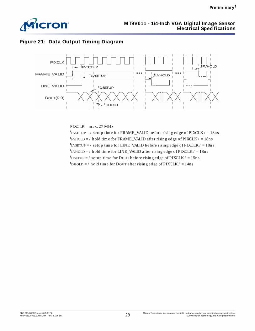
Figure 21: Data Output Timing Diagram
PIXCLK = max. 27 MHztFVSETUP = / setup time for FRAME_VALID before rising edge of PIXCLK / = 18nstFVHOLD = / hold time for FRAME_VALID after rising edge of PIXCLK / = 18nstLVSETUP = / setup time for LINE_VALID before rising edge of PIXCLK / = 18nstLVHOLD = / hold time for LINE_VALID after rising edge of PIXCLK / = 18nstDSETUP = / setup time for DOUT before rising edge of PIXCLK / = 15nstDHOLD = / hold time for DOUT after rising edge of PIXCLK / = 14ns
PIXCLK
FRAME_VALID
LINE_VALID
DOUT(9:0)
tDSETUP
tDHOLD
tFVHOLD
tLVHOLD
tFVSETUP
tLVSETUP
PDF: 817d5189/Source: 817d5173 Micron Technology, Inc., reserves the right to change products or specifications without notice.MT9V011_C82S_2_PLCC.fm - Rev. B 1/05 EN 28 ©2004 Micron Technology, Inc. All rights reserved.
MT9V011 - 1/4-Inch VGA Digital Image SensorElectrical Specifications
Preliminary‡
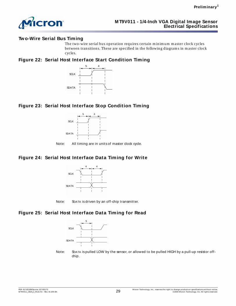
Two-Wire Serial Bus TimingThe two-wire serial bus operation requires certain minimum master clock cycles between transitions. These are specified in the following diagrams in master clock cycles.
Figure 22: Serial Host Interface Start Condition Timing
Figure 23: Serial Host Interface Stop Condition Timing
Note: All timing are in units of master clock cycle.
Figure 24: Serial Host Interface Data Timing for Write
Note: SDATA is driven by an off-chip transmitter.
Figure 25: Serial Host Interface Data Timing for Read
Note: SDATA is pulled LOW by the sensor, or allowed to be pulled HIGH by a pull-up resistor off-chip.
SCLK
5
SDATA
4
SCLK
5
SDATA
4
SCLK
4
SDATA
4
SCLK
5
SDATA
PDF: 817d5189/Source: 817d5173 Micron Technology, Inc., reserves the right to change products or specifications without notice.MT9V011_C82S_2_PLCC.fm - Rev. B 1/05 EN 29 ©2004 Micron Technology, Inc. All rights reserved.
MT9V011 - 1/4-Inch VGA Digital Image SensorElectrical Specifications
Preliminary‡
Figure 26: Acknowledge Signal Timing After an 8-bit Write to the Sensor
Figure 27: Acknowledge Signal Timing After an 8-bit Read from the Sensor
Note: After a read, the master receiver must pull down SDATA to acknowledge receipt of data bits. When read sequence is complete, the master must generate a no acknowledge by leaving SDATA to float high. On the following cycle a start or stop bit may be used.
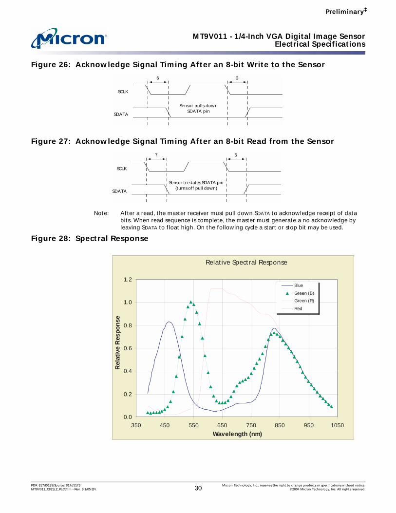
Figure 28: Spectral Response
SCLK
Sensor pulls downSDATA pin
6
SDATA
3
SCLK
Sensor tri-states SDATA pin(turns off pull down)
7
SDATA
6
0.0
0.2
0.4
0.6
0.8
1.0
1.2
350 450 550 650 750 850 950 1050Wavelength (nm)
Rel
ativ
e R
espo
nse
Blue
Green (B)Green (R)
Red
Relative Spectral Response
PDF: 817d5189/Source: 817d5173 Micron Technology, Inc., reserves the right to change products or specifications without notice.MT9V011_C82S_2_PLCC.fm - Rev. B 1/05 EN 30 ©2004 Micron Technology, Inc. All rights reserved.

MT9V011 - 1/4-Inch VGA Digital Image SensorElectrical Specifications
Preliminary‡
Figure 29: Image Center Offset
Note: Not to scale.
Image Center
Chip Center
PixelArray
Pixel (0,0)
697.4um
14.6um
Sensor Chip
PDF: 817d5189/Source: 817d5173 Micron Technology, Inc., reserves the right to change products or specifications without notice.MT9V011_C82S_2_PLCC.fm - Rev. B 1/05 EN 31 ©2004 Micron Technology, Inc. All rights reserved.

MT9V011 - 1/4-Inch VGA Digital Image SensorData Sheet Designation
Preliminary‡
Figure 30: 28-Pin PLCC Package Outline Drawing
Note: All dimensions are in millimeters.
Data Sheet DesignationPreliminary: This data sheet contains initial characterization limits that are subject to change upon full characterization of production devices.
2.35 ±0.15
SEATINGPLANE
SECTION A–A
0.08
0.70 ±0.05
128
1.27 TYP
A
7.62
LID MATERIAL: BOROSILICATE GLASS
LEAD FINISH: GOLD PLATING, 20 MICRO INCHES MINIMUM THICKNESS
SUBSTRATE MATERIAL: FR4 RESIN1.27 TYP
7.62
A
1.70 ±0.10
11.43 ±0.10
0.64 TYP
29X R0.225
27X 1.272.16
0.350 ±0.050
1.450 ±0.075
0.55 ±0.05
8X 1.905 ±0.100
11.43 ±0.100.08
®
8000 S. Federal Way, P.O. Box 6, Boise, ID 83707-0006, Tel: [email protected] www.micron.com Customer Comment Line: 800-932-4992
Micron, the M logo, and the Micron logo are trademarks of Micron Technology, Inc. All other trademarks are the property of their respective owners.
Preliminary: This data sheet contains initial characterization limits that are subject to change upon full characterization of production devices.
PDF: 817d5189/Source: 817d5173 Micron Technology, Inc., reserves the right to change products or specifications without notice.MT9V011_C82S_2_PLCC.fm - Rev. B 1/05 EN 32 ©2004 Micron Technology, Inc. All rights reserved.

MT9V011 - 1/4-Inch VGA Digital Image SensorRevision History
Preliminary‡
Revision HistoryRev B, Preliminary ...........................................................................................................................................................1/05
• Updated part number: MT9V011P11STC:B• Changed chip version ID registers (R0x00/0xFF) from 0x8232 to 0x8243 in Table 6 on page 15 and Table 7 on
page 17• Table 10 on page 25: Replaced VPWR with VDD, updated IOH and IOL maximum values; added Note 2• Table 11 on page 26: Updated definition for parameter tOH • Updated Figure 2 on page 5, Figure 19 on page 27, Figure 20 on page 27, and Figure 21 on page 28
Rev A, Preliminary ...........................................................................................................................................................4/04• Initial release of document
PDF: 817d5189/Source: 817d5173 Micron Technology, Inc., reserves the right to change products or specifications without notice.MT9V011_C82S_2_PLCC.fm - Rev. B 1/05 EN 33 ©2004 Micron Technology, Inc. All rights reserved.